

SONY KV-HS29M61, KV-HS29M90, KV-HS29M91, KV-HS34M61, KV-HS34M90 Service Manual
...
SERVICE MANUAL
AG-3F
CHASSIS
MODEL COMMANDER DEST. CHASSIS NO.
KV-HS29M61 RM-997 ES SCC-M03-A
KV-HS29M90 RM-997 HK SCC-P96-C
KV-HS29M91 RM-997 ME SCC-P98-C
KV-HS34M61 RM-997 GE SCC-P97-A
KV-HS34M61 RM-997 S SCC-M01-A
KV-HS34M90 RM-997 HK SCC-P96-A
MODEL COMMANDER DEST. CHASSIS NO.
KV-HS34M91 RM-997 ME SCC-P98-A
KV-HS38M61 RM-997 GE SCC-P97-B
KV-HS38M61 RM-997 S SCC-M01-B
KV-HS38M90 RM-997 HK SCC-P96-B
KV-HS38M91 RM-997 ME SCC-P98-B
VIDEO
A/B
DRC-MF
V CENTER
INDEX
PROG
MENU
HD/DVD
123
456
7809
JUMP
PROG
OPTION RESET
TV
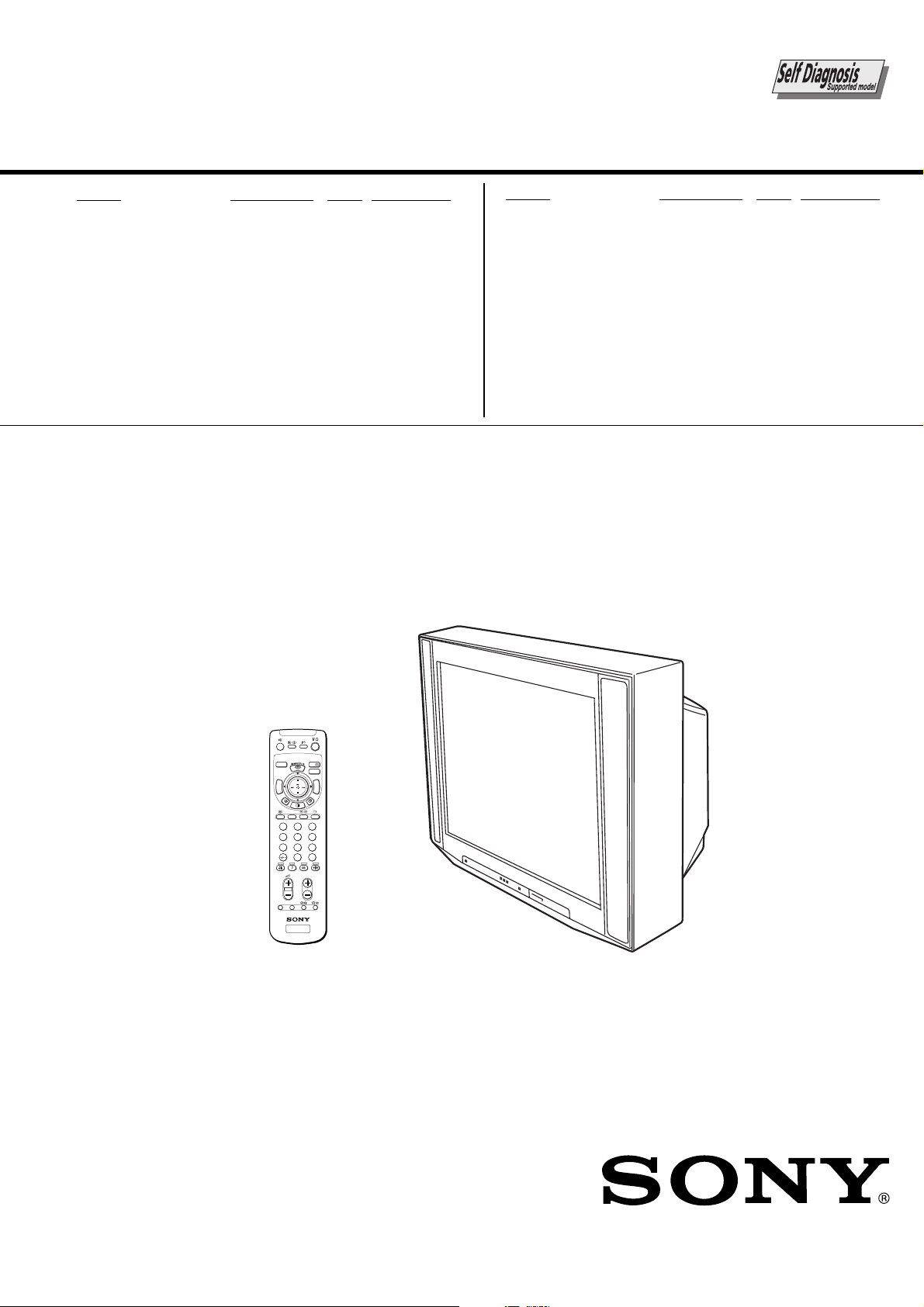
RM-997 KP-HS29M61/M90/M91,
KP-HS34M61/M90/M91,
KP-HS38M61/M90/M91
TRINITRON® COLOR TV
KV-HS29M61/M90/M91, HS34M61/M90/M91, HS38M61/M90/M91
SPECIFICATIONS
KV-HS29M61/M91 KV-HS29M90
KV-HS34M61/M91 KV-HS34M90 KV-HS38M61/M90/M91
Power requirements 110-240 V AC, 50/60 Hz 220V AC, 50Hz 220-240 V AC, 50/60 Hz
Power consumption (W) Indicated on the rear of the TV.
Television system B/G, I, D/K, M
Color system PAL, PAL 60, SECAM, NTSC4.43, NTSC3.58
Stereo system NICAM Stereo/Bilingual B/G, I; A2 Stereo (German) B/G
Channel coverage
B/G VHF: E2 to E12 / UHF: E21 to E69 / CATV: S01 to S03, S1 to S41
I UHF: B21 to B68 / CATV: S01 to S03, S1 to S41
D/K VHF: C1 to C12, R1 to R12 / UHF: C13 to C57, R21 to R60
CATV: S01 to S03, S1 to S41, Z1 to Z39
M VHF: A2 to A13 / UHF: A14 to A79 /
CATV: A-8 to A-2, A to W+4, W+6 to W+84
˘ (Antenna) 75-ohm external terminal
Audio output (Speaker) 15W + 15W (12W + 12W : 7 % distortion)
Number of terminal
(Video) Input: 4 Output: 1 Phono jacks; 1 Vp-p, 75 ohms
≥ (Audio) Input: 4 Output: 1 Phono jacks; 500 mVrms
(S Video) Input: 2 Y : 1 Vp-p, 75 ohms,
unbalanced, sync negative
C : 0.286 Vp-p, 75 ohms
(Component Input: 2 Phone jacks
Video) Y : 1 Vp-p, 75 ohms, sync negative
: 0.7 Vp-p, 75 ohms
C
B
: 0.7 Vp-p, 75 ohms
C
R
Audio : 500 mVrms
(R/G/B/HD/ Input: 1 Phone jacks
VD Video) R : 0.7 Vp-p, 75 ohms
B : 0.7 Vp-p, 75 ohms
G : 0.7 Vp-p, 75 ohms
HD : 0.7 Vp-p, 75 ohms
VD : 0.7 Vp-p, 75 ohms
2 (Headphones) Output: 1 Stereo minijack
Picture tube 29 inch 34 inch 38 inch
Tube size (cm) 72 86 97
(Measured diagonally)
Dimension (w/h/d, mm) 772 × 587 × 562 898 × 678 × 581 994 × 755 × 623
Mass (kg) 58 86 112
Design and specifications are subject to change without notice.
RM-997
CAUTION
SHORT CIRCUIT THE ANODE OF THE PICTURE TUBE AND
THE ANODE CAP TO THE METAL CHASSIS, CRT SHIELD, OR
CARBON PAINTED ON THE CRT, AFTER REMOVING THE
ANODE.
SAFETY-RELATED COMPONENT WARNING!!
COMPONENTS IDENTIFIED BY SHADING AND MARK ! ON
THE SCHEMATIC DIAGRAMS, EXPLODED VIEWS AND IN THE
PARTS LIST ARE CRITICAL TO SAFE OPERATION. REPLACE
THESE COMPONENTS WITH SONY PARTS WHOSE PART
NUMBERS APPEAR AS SHOWN IN THIS MANUAL OR IN
SUPPLEMENTS PUBLISHED BY SONY.
– 2 –

KV-HS29M61/M90/M91, HS34M61/M90/M91, HS38M61/M90/M91
RM-997
TABLE OF CONTENTS
Section Title Page
SELF DIAGNOSIS FUNCTION .................................. 4
1. DISASSEMBLY
1-1. Rear Cover Removal .............................................. 8
1-2. Speaker Box Removal ............................................ 8
1-3. Chassis Assy Removal ............................................. 8
1-4. Service Position ....................................................... 9
1-5. DC Board Removal.................................................. 9
1-6. J Board Removal ...................................................... 9
1-7. D Board Removal .................................................. 10
1-8. A, A1, and E Boards and B4 Block Removal ...... 10
1-9. H1, H2, MS2, and F2 Boards Removal ................ 11
1-10. Picture Tube Removal (1)...................................... 11
1-11. Picture Tube Removal (2)...................................... 12
1-12. Harness Ranning .................................................... 13
2. SET-UP ADJUSTMENTS
2-1. Beam Landing Adjustment .................................... 15
2-2. Convergence Adjustment....................................... 16
2-3. Focus Adjustment .................................................. 18
2-4. Neck Assy Twist Adjustment ................................. 18
2-5. G2 (Screen) and White Blance Adjustments ......... 19
Section Title Page
4. SAFETY RELATED ADJUSTMENTS
4-1. HV Regulation Adjustment .................................... 38
4-2. HV Hold-down Adjustment ................................... 38
4-2-1. HV Protector Adjustments ................................ 38
4-2-2. HV Protector Check ......................................... 38
4-3. +B Max Voltage Confirmation ............................... 39
4-4. +B OVP Confirmation ........................................... 39
5. DIAGRAMS
5-1. Block Diagrams ...................................................... 40
5-2. Circuit Boards Location ......................................... 56
5-3. Schematic Diagrams ............................................... 57
5-4. Semiconductors .................................................... 124
6. EXPLODED VIEWS
6-1. Picture Tube .......................................................... 128
6-2. Chassis .................................................................. 130
6-3. Packing Materials ................................................. 132
7. ELECTRICAL PARTS LIST ................................... 133
3. CIRCUIT ADJUSTMENTS
3-1. Adjustments with Commander .............................. 20
3-2. Adjustment Method ............................................... 21
3-3. Picture Quality Adjustments.................................. 35
3-3-1. Preparation ......................................................... 35
3-3-2. NTSC Video Input ............................................. 36
3-3-3. NTSC RF Input ................................................. 36
3-3-4. PAL Video Input ................................................ 37
3-3-5. PAL RF Input ..................................................... 37
– 3 –
KV-HS29M61/M90/M91, HS34M61/M90/M91, HS38M61/M90/M91
RM-997
SELF DIAGNOSTIC FUNCTION
The units in this manual contain a self-diagnostic function. If an error occurs, the STANDBY/TIMER lamp will automatically
begin to flash.
The number of times the lamp flashes translates to a probable source of the problem. A definition of the STANDBY/TIMER
lamp flash indicators is listed in the instruction manual for the user’s knowledge and reference. If an error symptom cannot
be reproduced, the remote commander can be used to review the failure occurrence data stored in memory to reveal past
problems and how often these problems occur.
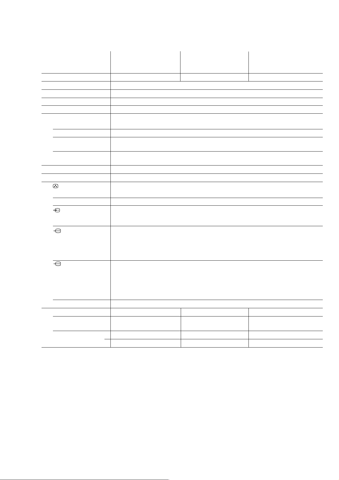
1. DIAGNOSTIC TEST INDICATORS
When an errors occurs, the STANDBY/TIMER lamp will flash a set number of times to indicate the possible cause of the
problem. If there is more than one error, the lamp will identify the first of the problem areas.
Result for all of the following diagnostic items are displayed on screen. No error has occured if the screen displays a “0”.
Diagnostic
Item
Description
• Power does not
turn on
• +B overcurrent
(OCP) or
• +B overvoltage
(OVP)
• Vertical deflection
failure
• White balance
failure
(no PICTURE)
• Horizontal
deflection failure
No. of times
STANDBY/TIMER
lamp flashes
Does not light
2 times
3 times
4 times
5 times
6 times
Self-diagnostic
display/Diagnostic
result
—
002:000 or
002:001~255
003:000 or
003:001~255
004:000 or
004:001~225
005:000 or
005:001~225
006:000 or
006:001~225
Probable
Cause
Location
• Power cord is not plugged
in.
• Fuse is burned out F1601
(F1 Board)
• H.OUT Q5030 is shorted.
• Q5003(PWM-OUT) is
shorted.
• PH 6502 faulty.
• 135V Line is overvoltage
supplied. (D board)
• V.OUT IC5004 faulty
D5001 faulty
D5002 faulty
D5035 faulty
D5036 faulty
R5173 or R5172 open.
• G2 is improperly adjusted.
(Note 2)
• CRT problem.
• Video OUT IC9001,9002,
9003 are faulty. (C1 board)
• IC4301 (E board) are faulty.
• No connection E board to
C1 board.
• C5064 is open circuit.
• CN5002(D board) is
disconnected.
• HOP circuit is failure.
• -10.2V Power Supply or
IC2601 or IC2602 are
failure.
• CN6101 (D board) is
disconnected
Detected
Symptoms
• Power does not come on.
• No power is supplied to the
TV.
• AC power supply is faulty.
• Power does not come on.
• Load on power line is
shorted.
• Power does not come on.
• Vertical deflection pulse is
stopped.
• Vertical size is too amall.
• Vertical deflection stopped.
• Power line is shorted or
power supply is stopped.
• No raster is generated.
• CRT cathode current
detection reference pulse
output is small.
• H pulse output is too high.
• Low B (-10.5V) is too Low.
• Audio Protection
• Micro reset
Note 1: If a + B overcurrent is detected, stoppage of the vertical deflection is detected simultaneously.
The symptom that is diagnosed first by the microcontroller is displayed on the screen.
Note 2: Refer to screen (G2) Adjustment in section 3-4 of this manual.
7 times
-
007:000 or
007:001~22500
101:00 or
101:001~225
• Power Supply fails.
• IC2003, IC1204 faulty.
• Discharge CRT (C1 Board)
• Static discharge
• External noise
• There is picture but speaker
does not release sound.
• Power is shut down shorlty,
after this return back
tonormal
• Detect Micro latch up.
– 4 –
KV-HS29M61/M90/M91, HS34M61/M90/M91, HS38M61/M90/M91
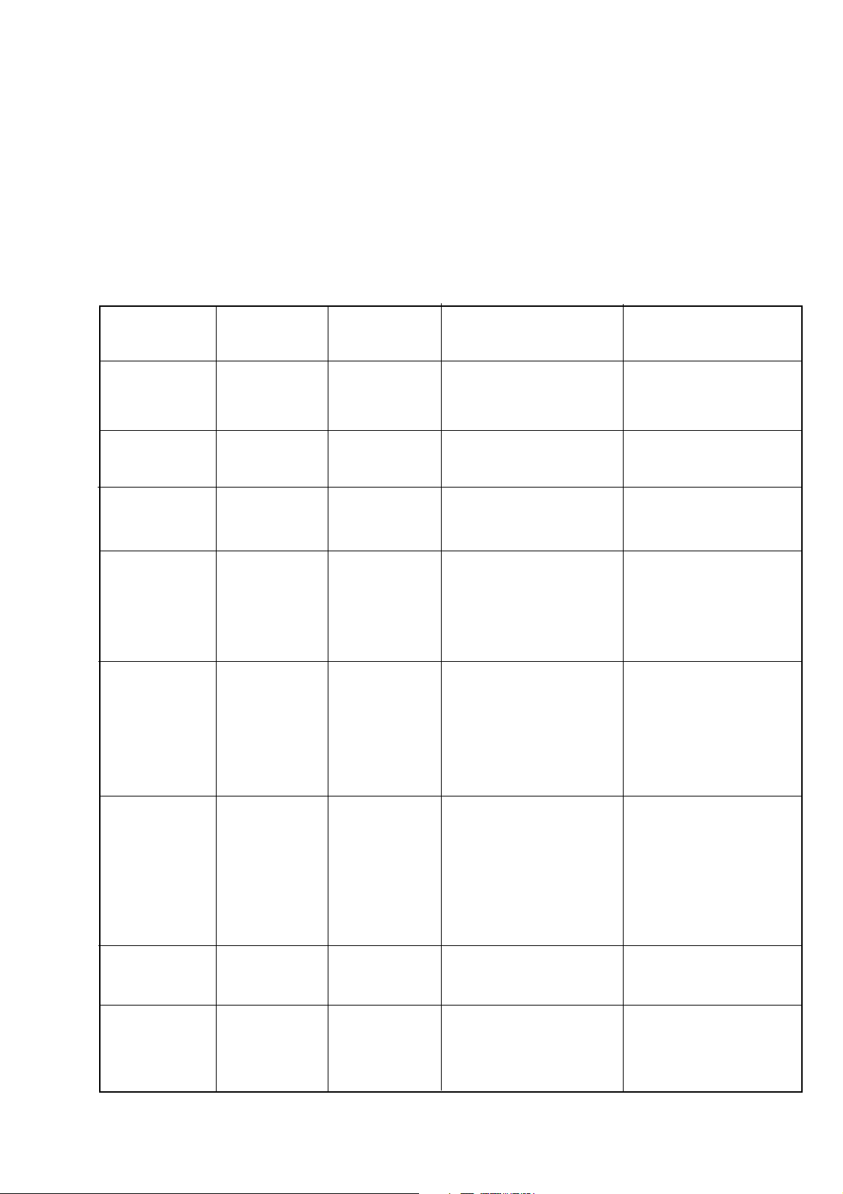
2. DISPLAY OF STANDBY/TIMER LIGHT FLASH COUNT
2 times
5 times
Lamp ON 0.3 sec.
Lamp OFF 0.3 sec.
4 times
5 times
6 times
7 times
• One flash count is not used for self-diagnostic.
RM-997
Lamp OFF 3 sec.
STANDBY/SLEEP lamp
Diagnostic Item Flash Count*
+B overcurrentovervoltage 2 times
+B overvoltage 3 times
V deflection stop 4 times
White balance failure 5 times
High voltage protecter 6 times
Audio protection 7 times
* One flash count is not used for self-diagnostic.
3. STOPPING THE STANDBY/TIMER FLASH
Turn off the power switch on the TV main unit or unplug the power cord from the outlet to stop the STANDBY/TIMER lamp
from flashing.
– 5 –
KV-HS29M61/M90/M91, HS34M61/M90/M91, HS38M61/M90/M91
RM-997
4. SELF-DIAGNOSTIC SCREEN DISPLAY
For errors with symptoms such as “power sometimes shuts off” or “screen sometimes goes out” that cannot be confirmed,
it is possible to bring up past occurances of failure for confirmation on the screen:
[To Bring Up Screen Test]
In standby mode, press buttons on the remote commander sequentially in rapid succession as shown below:
[Screendisplay] / channel [5] / Sound volume [-] / Power ON
˘
Note that this differs from entering the service mode (mode volume [+]).
Self-Diagnosis screen display
SELF DIAGNOSTIC
002 : 000
003 : 000
004 : 000
005 : 001
006 : 002
007 : 000
101 : 000
Numeral "0" means that no fault has been detected.
Numeral "1" means a fault has been detected.
Numeral "2" means two faults have been detected.
5. HANDLING OF SELF-DIAGNOSTIC SCREEN DISPLAY
Since the diagnostic results displayed on the screen are not automatically cleared, always check the self-diagnostic
screen during repairs. When you have completed the repairs, clear the result display to “0”.
Unless the result display is cleared to “0”, the self-diagnostic function will not be able to detect subsequent faults after
completion of the repairs.
[Clearing the result display]
To clear the result display to “0”, press buttons on the remote commander sequentially as shown below when the diagnostic screen is being displayed.
Channel [8] / 0
[Quitting Self-diagnostic screen]
To quit the entire self-diagnostic screen, turn off the power switch on the remote commander or the main unit.
– 6 –
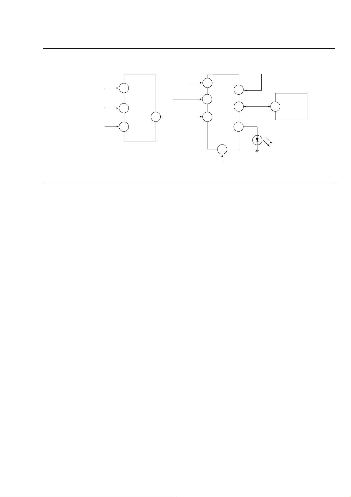
6. SELF-DIAGNOSTIC CIRCUIT
RGB JUNGLE
FROM
CRT(IK)
Q5018, D8035
(D Board)
Q5010
(D Board)
24
57
56
IC4300
CXA2170Q
IK-IN
HPROT
SDA0
V PROT
KV-HS29M61/M90/M91, HS34M61/M90/M91, HS38M61/M90/M91
RM-997
OVP
OCP
IC001
SYSTEM
5
V PROT
H PROT
8
V PROT
4652
IO-SDAT
LED
Au PROT
100
IC1203,1240
(A Board)
87
22
IC2602
( A Board)
SDA1
IC003
MEMORY
515
[+BovercurrentªOCPº] Occurs when an overcurrent on the +B(135) line is detected by Q5004(D board). If
Q6610(D board) go to ON, the voltage to pin 5 of IC001(A board) go to UP. The unit
will automatically turn off.
[+BovervoltageªOVPº] Occurs when an overdrive on the +B(135V) line is detected by D6635(D board), Q6611
and Q6619. If Q6611 go to ON, the voltage to pin 8 of IC001 go to UP. The unit will
automatically turn off.
[Verticaldeflectionfailure] Occurs when an absence of the vertical deflection pulse is detected by Q5010. Shut
down the power supply.
[Whitebalancefailure] If the RGB levels do not balance or become low level within 5 seconds. This error will
be detected by IC4300. TV will stay on, but there will be no picture.
[HighvoltageundervoltageprotectionªHVUVPº]
High-voltage undervoltage conditions may indicate defective transformer, rectifiers,
CRT or fault within the power supply circuit. When high-voltage drops for any reason,
so does the voltage at T8001.17 and buffer IC8004.7. The malfunction is detected by
comparator IC8006A that generates high logic signal labeled H PROT. This signal is
sent via D8014 to the H prot that opens contacts of the AC relay RY6501 and turns off
main power.
[AudioProtector] If the Audio out line became DC. This error will be detected by Q1211, Q1209, and
Q1210.The unit will automatically turn off.
– 7 –
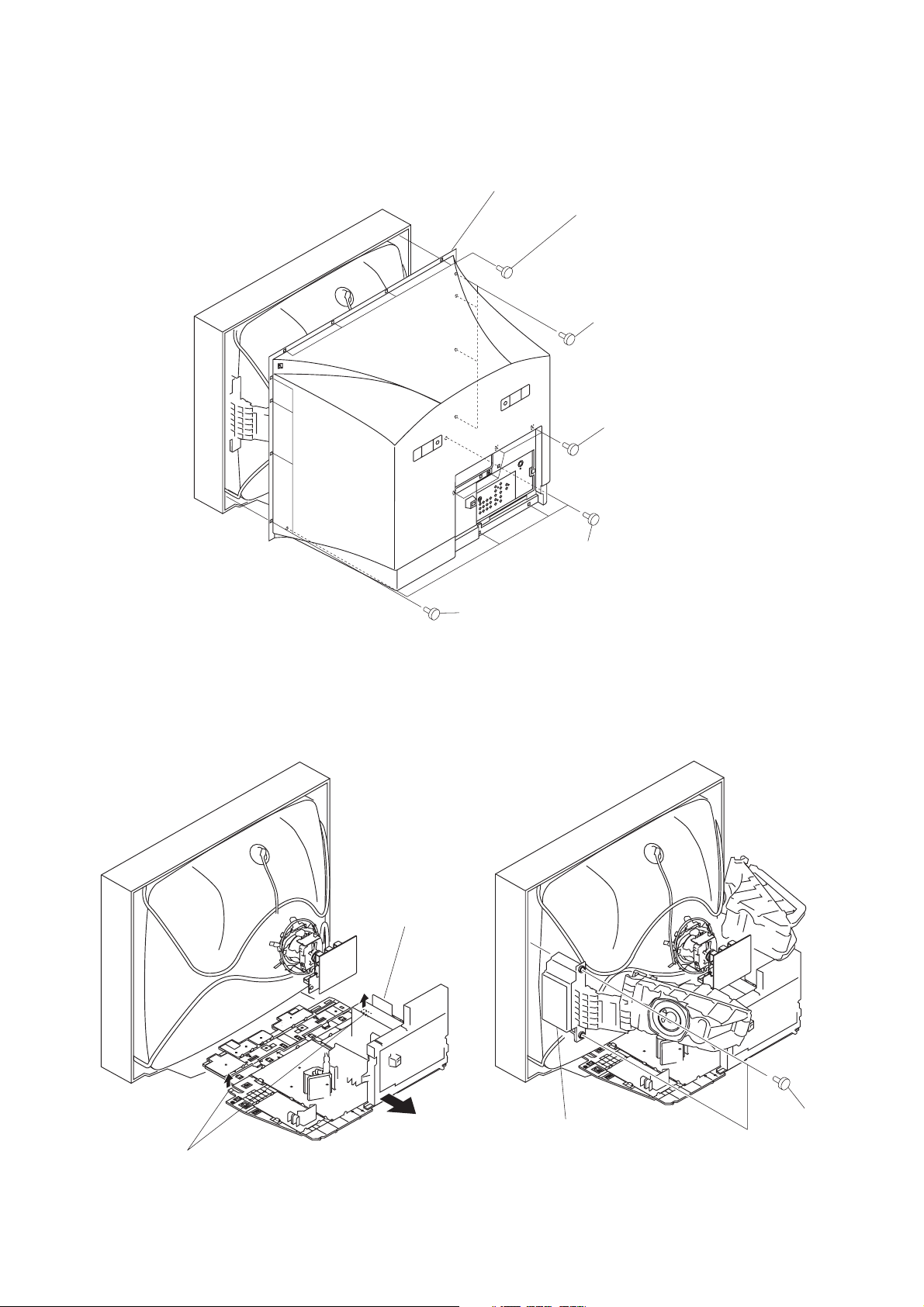
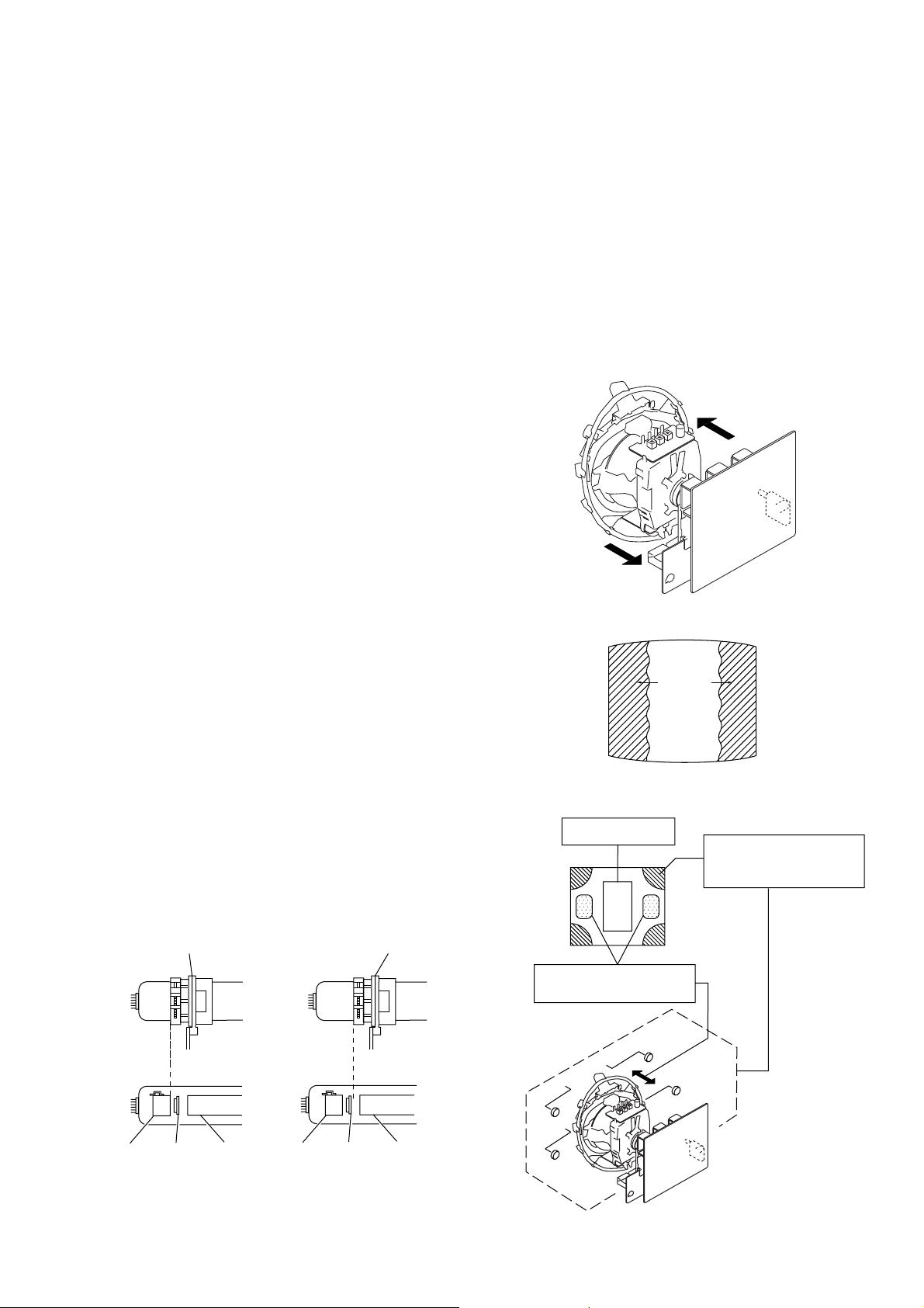
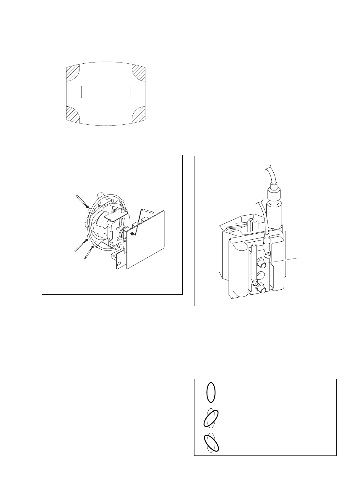
1-1. REAR COVER REMOVAL
KV-HS29M61/M90/M91, HS34M61/M90/M91, HS38M61/M90/M91
RM-997
SECTION 1
DISASSEMBLY
2 Rear cover
1 Four screws (KV-HS38M90)
(+BVTP 4X16)
1 Four screws (KV-HS29/34M90)
(+BVTP 4X16)
1 Four screws (KV-HS38M90)
(+BVTP 4X16)
1 Two screws (KV-HS29/34M90)
(+BVTP 4X16)
1 Four screws
(+BVTP 4X16)
1-2. SPEAKER BOX REMOVAL
1 Four screws
(+BVTP 4X16)
1 Four screws (KV-HS38M90)
(+BVTP 4X16)
1 Two screws (KV-HS29/34M90)
(+BVTP 4X16)
1-3. CHASSIS ASSY REMOVAL
2 Chassis assy
1 Claws (Main bracket)
– 8 –
2 Arm (R) block assy
1 Two screws
(+PWHTP 4X25)
KV-HS29M61/M90/M91, HS34M61/M90/M91, HS38M61/M90/M91
RM-997
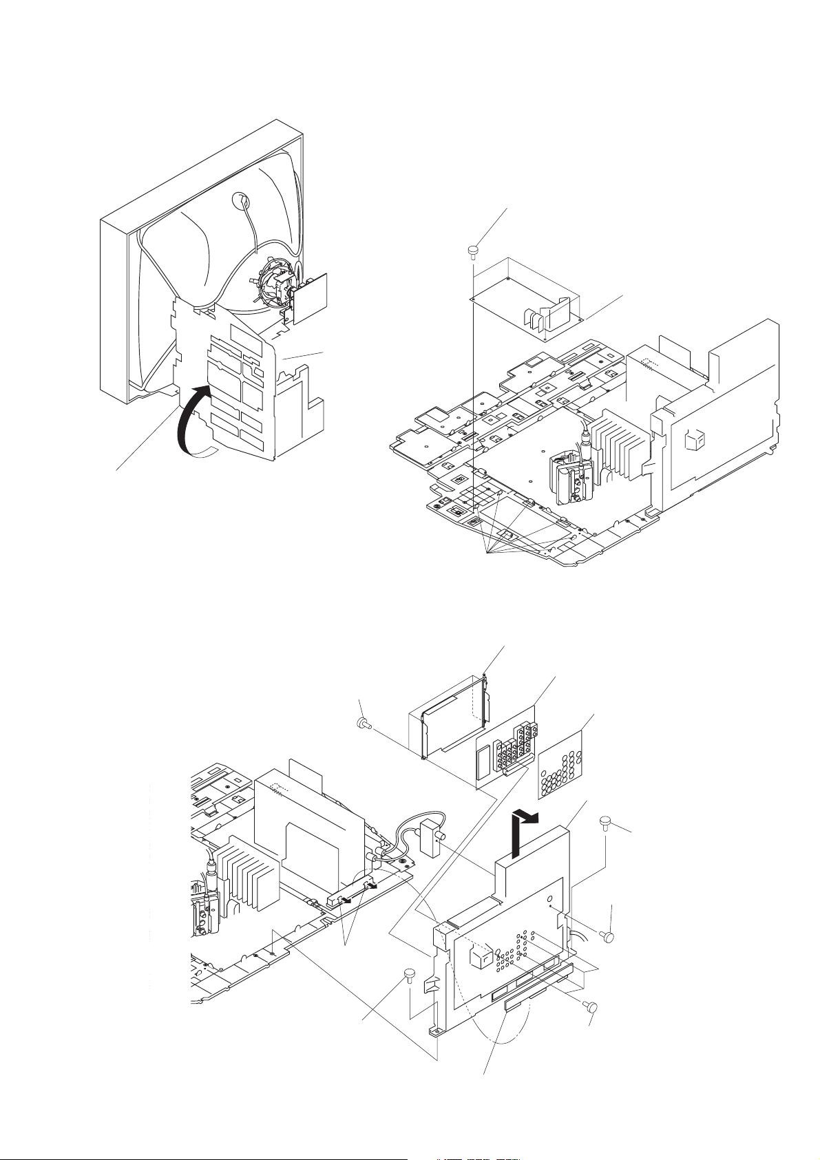
1-4. SERVICE POSITION
2 Chassis assy
1-5. DC BOARD REMOVAL
1 Four screws
(+BVTP 3X12)
2 DC board
1 Mounting side
1-6. J BOARD REMOVAL
8 Four screws
(+BVTP 3X12)
6 Claws
Claws
9 Shield plate J
! J board
Shield
7 J blacket
1 Screw
(+BVTP 3X12)
2 Screw
(+PSW 3X6)
1 Screw
(+BVTP 3X12)
3 Four screws
(+BVTP 3X12)
5 J Cover
– 9 –
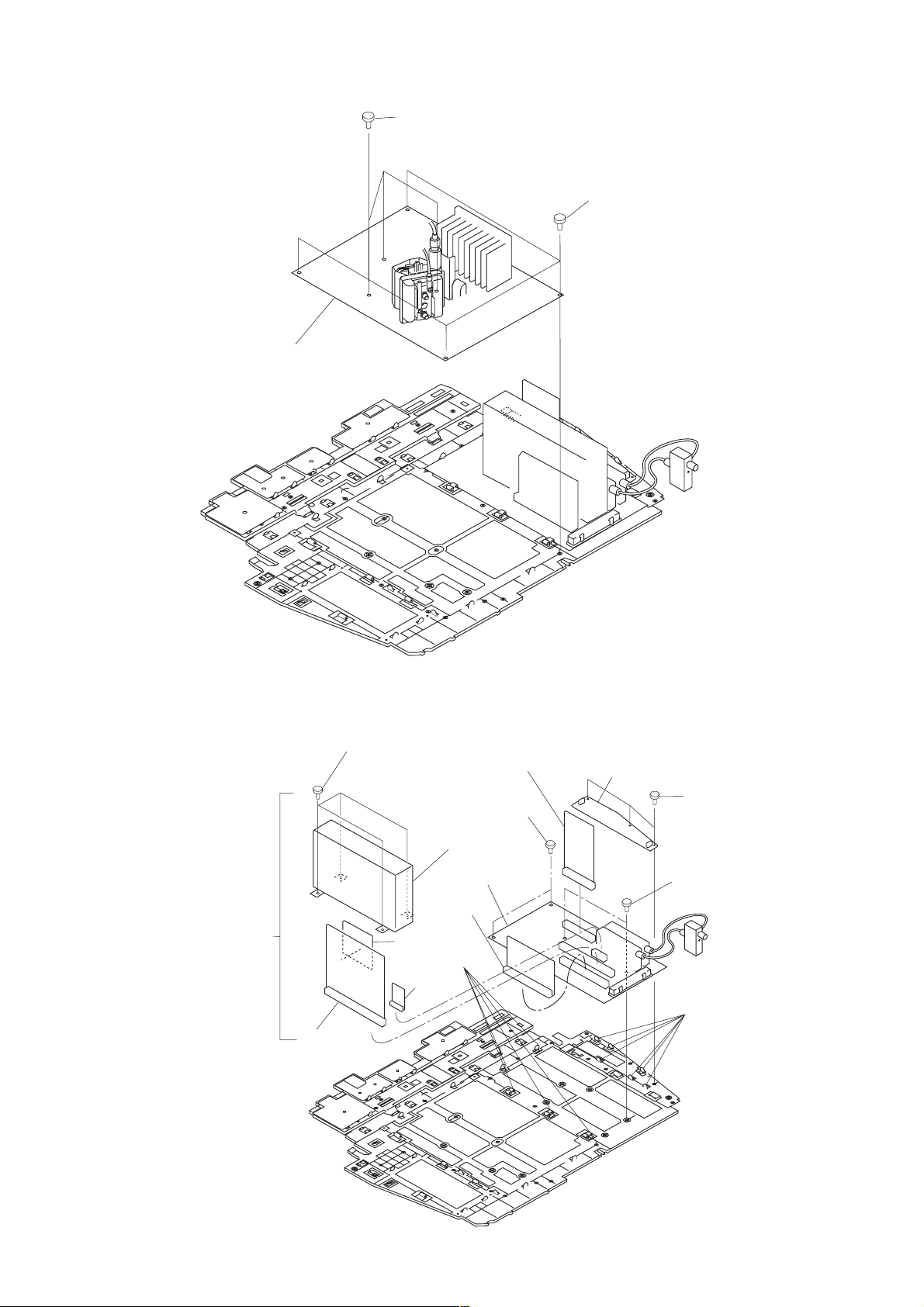
1-7. D BOARD REMOVAL
3 D board
KV-HS29M61/M90/M91, HS34M61/M90/M91, HS38M61/M90/M91
RM-997
2 Three crews
(+BVTP 3X12)
1 Four screws
(+BVTP 3X12)
1-8. A, A1, V2 AND E BOARDS, AND B4 BLOCK REMOVAL
6 Four screws
B4 block
(+BVTP 3X12)
BM1C board
V2 board
8 B4 board
5 A1 board
1 Two screws
(+BVTP 3X12)
7 Shield cover
2 A board
9 E board
Claws
4 F1 board
3 Three screws
(+BVTP 3X12)
1 Two screws
(+BVTP 3X12)
Claws
– 10 –
KV-HS29M61/M90/M91, HS34M61/M90/M91, HS38M61/M90/M91
1-9. H1, H2, MS2, AND F2 BOARDS REMOVAL
5 Screw
(+BVTP 3X12)
3 Two screws
(+BVTP 3X12)
RM-997
6 H1 board
7 Screw
(+BVTP 3X12)
1 Screw
(+BVTP 3X12)
4 MS2 board
2 F2 board
Claws
Claws
1-10. PICTURE TUBE REMOVAL (1)
8 H2 board
Claws
Claws
3 Tension spring
5 DGC Clip (34")
5 DGC Clip (29")
5 DGC Clip (38")
2 Degauss coil (with LCC)
1 DGC Holder (34"/38")
1 DGC Holder (29")
2 Degauss coil (with LCC)
4 CRT Supporter
– 11 –
1-11. PICTURE TUBE REMOVAL (2)
KV-HS29M61/M90/M91, HS34M61/M90/M91, HS38M61/M90/M91
RM-997
1 C1 board
2 V board (34"/38")
V3 board (29")
3 NA Rotation coil
5 CRT
4 Tapping screw (with Crown washer)
– 12 –
1-12. HARNESS RANNING
NS Coil
SP (L)
< F2 board >
CN1903
CN902
KV-HS29M61/M90/M91, HS34M61/M90/M91, HS38M61/M90/M91
Degauss coil (with LCC)
LCC Coil
Degauss coil (with LCC)
SP (R)
To C1 board
CN1901
< MS2 board >
CN1402
< H1 board >
CN1980
CN1933
< H2 board >
CN1935
CN1934
CN1932
RM-997
To
NS Coil
CN5801
CN5805
CN5802
< DC board >
CN5803
CN5808
CN5403
CN5806
CN5807
CN5901
CN6605
CN6603
CN6604
< D board >
CN5002
CN6503
CN5003
CN5509
CN5506
CN5505
CN5011
CN6101
CN5009
CN5001
CN5801
< V board >
CN1162
CN4302
CN4305
< E board >
CN9101
CN9102
CN1161
CN1164
CN1160
CN101
CN1163
< B4 board >
< J board >
CN1293
< A board >
CN402
<BM1C
board >
< V2 board >
CN1101
TU101
CN1196
CN1190
TU3301
CN1100
< E board >
CN1603
< F1 board >
CN1604
CN1601
AC Cord
CN1602
CN9002
CN9001
< C1 board >
J9001
– 13 –
KV-HS29M61/M90/M91, HS34M61/M90/M91, HS38M61/M90/M91
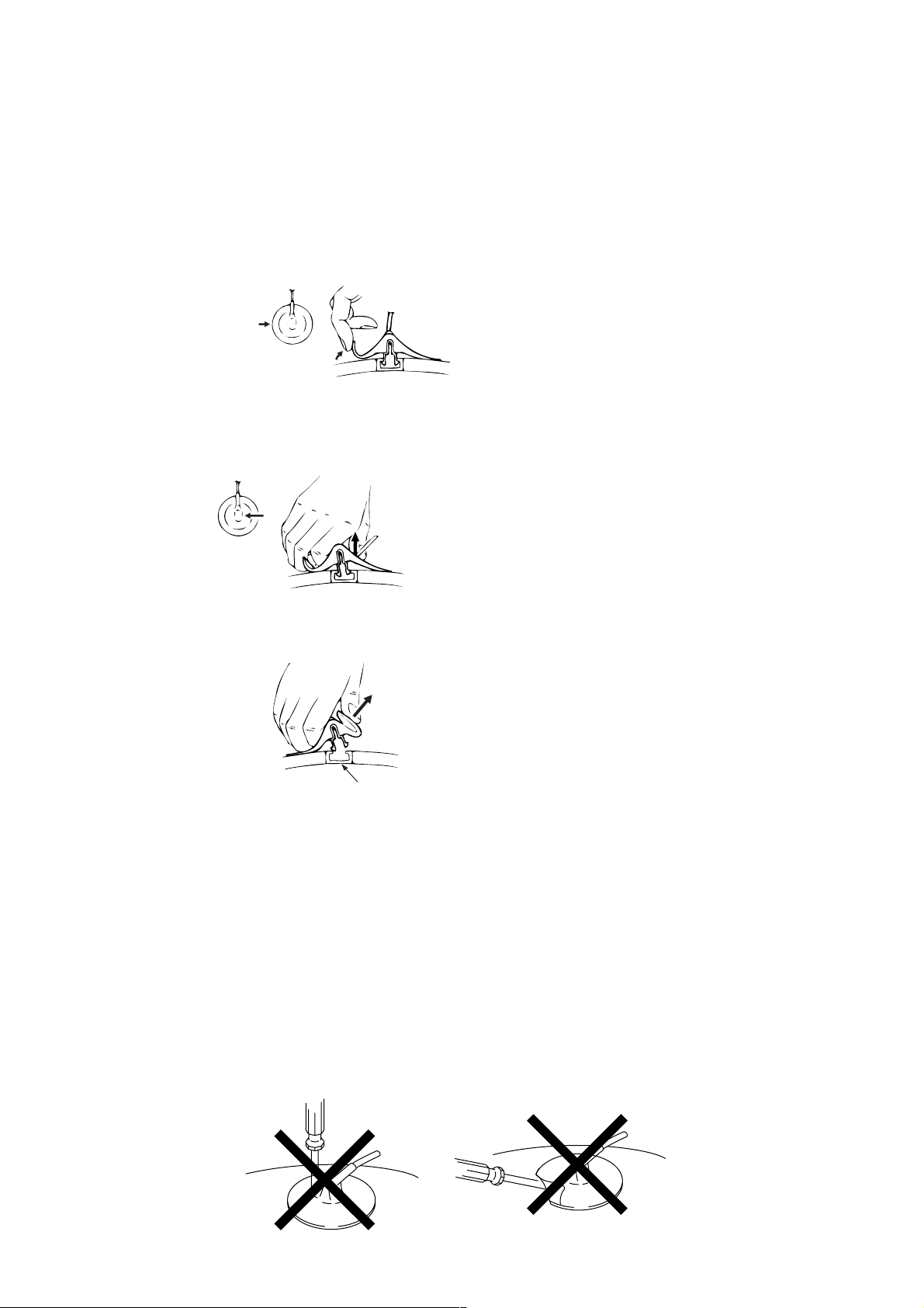
• REMOVAL OF ANODE-CAP
NOTE : After removing the anode, short circuit the anode of
the picture tube and the anode cap to the metal chassis, CRT shield or carbon paint on the CRT.
• REMOVING PROCEDURES
a
a
1 Tern up one side of the rubber cap in the direction indicated
by the arrow a.
RM-997
b
2 Using a thumb pull the rubber cap firmly in the direction
indicatid by the arrow b.
c
Anode button
3 When one side of the rubber cap is separated from the
anode button, the anode-cap can be removed by terning up
the rubber capand pulling it up in the directin off the arrow
c.
• HOW TO HANDLE AN ANODE-CAP
1 Do not damage the surface of anode-caps with sharp
shaped objects.
2 Do not press the rubber too hard so as not to damage the
inside of anode-cap.
A metal fitting called the shatter-hook terminal is built
into the rubber.
3 Do not turn the foot of rubber over too hard.
The shatter-hook terminal will stick out or damage the
rubber.
– 14 –
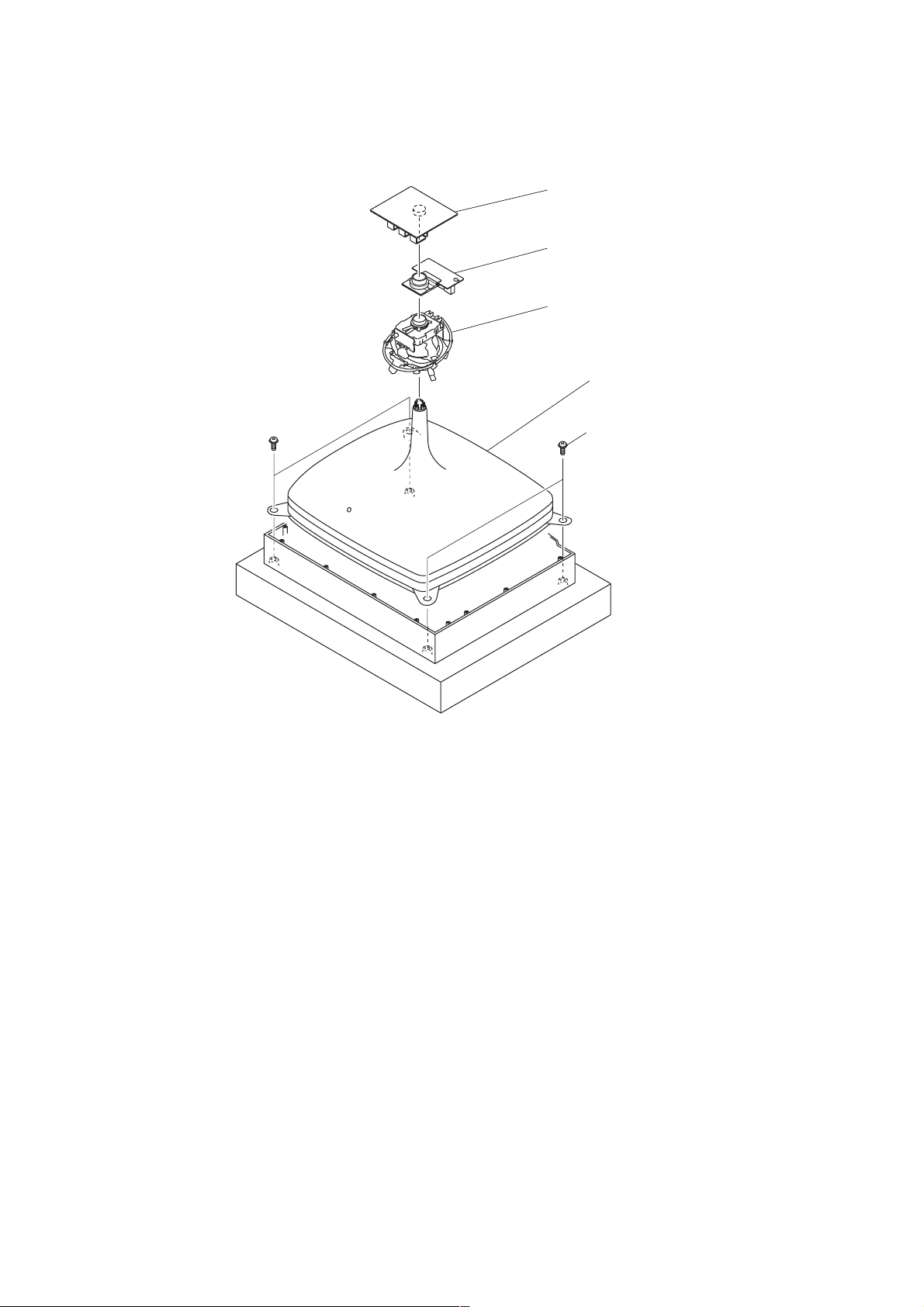
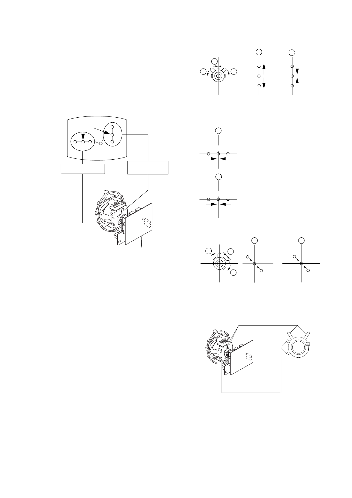
KV-HS29M61/M90/M91, HS34M61/M90/M91, HS38M61/M90/M91
Purity control
corrects this area.
Disk magnets or rotatable
disk magnets correct these
areas (a-d).
Deflection yoke positioning
corrects these areas.
a
b
c
d
b
c
d
a
RM-997
SECTION 2
SET-UP ADJUSTMENTS
• The following adjustments should be made when a complete
• These adjustments should be performed with rated power
Controls and switches should be set as follows unless otherwise
noted:
PICTURE control ........................................................... normal
BRIGHTNESS control ................................................... normal
................................................................................................................................................................................................................................
Preparation :
• In order to reduce the influence of geomagnetism on the set's
• Switch on the set's power and degauss with the degausser.
2-1. BEAM LANDING ADJUSTMENT
1. Input a white signal with the pattern generator.
2. Position neck assy as shown in Fig3-1.
3. Set the pattern generator raster signal to a green raster.
4. Move the deflection yoke to the rear and adjust with the purity
5. Move the deflection yoke forward and adjust so that the entire
6. Switch the raster signal to blue, then to green and verify the
7. When the position of the deflection yoke has been decided,
8. If the beam does not land correctly in all the corners, use a
realignment is required or a new picture tube is installed.
supply voltage unless otherwise noted.
picture tube, face it east or west.
Contrast
Brightness
control so that the green is at the center and the blue and the
red take up equally sized areas on each side.
(See Figures 2-1 through 2-3.)
screen is green. (See Figure 2-2.)
condition.
fasten the deflection yoke with the screws and DY spacers.
magnet to adjust it.
(See Figure 2-4.)
Neck assy
normal
}
Neck assy
Perform the adjustments in the following order :
1. Beam Landing
2. Convergence
3. Focus
4. White Balance
Note : Test Equipment Required.
1. Color-bar/Pattern Generator
2. Degausser
3. Oscilloscope
Fig. 2-2
Blue
Red
Green
Fig. 2-3
Behind the G2 edge
G2G1 G3
Behind the G2 edge
G2G1 G3
<KV-HS29><KV-HS34/38>
Fig. 2-1
Fig. 2-4
– 15 –
KV-HS29M61/M90/M91, HS34M61/M90/M91, HS38M61/M90/M91
RM-997
2-2. CONVERGENCE ADJUSTMENT
Preparation :
• Before starting this adjustment, adjust the focus, horizontal size
and vertical size.
• Set the PICTURE and BRIGHTNESS 50%.
• Cross hatch / Dot pattern.
(1) Horizontal and Vertical Static Convergence
Center dot
R G B
H. STAT VR
R
G
B
V. STAT
Magnet
1 V. STAT
a
b b
2 H. STAT VR
a
RGGBB
b
a
B
G
R
R
b
B
G
R
C1 Board
1. (Moving horizontally), adjust the H.STAT control so that the
red, green and blue dots are on top of each other at the center
of the screen.
2. (Moving vertically), adjust the V.STAT magnet so that the red,
green and blue dots are on top of each other at the center of the
screen.
3. If the H.STAT variable resistor cannot bring the red, green and
blue dots together at the center of the screen, adjust the
horizontal convergence with the H.STAT variable resistor and
the V.STAT magnet in the manner given below.
(In this case, the H.STAT variable resistor and the V.STAT
magnet influence each other, so be sure to perform adjustments
while tracking.)
3
a
b
a
R
b
B
Purity
V.STAT
b
B
GG
R
– 16 –
KV-HS29M61/M90/M91, HS34M61/M90/M91, HS38M61/M90/M91
RM-997
4 BMC (Hexapole) Magnet.
If the red, green and blue dots are not balanced or aligned, then
use the BMC magnet to adjust in the manner described below.
RG B R G B R GB
RB
G
(2) Dynamic Convergence Adjustment
Preparation:
• Before starting this adjustment, adjust the horizontal static
convergence and the vertical static convergence
• Set the PICTURE and BRIGHTNESS to normal.
RG
GB
RB
4. Adjust YCH.
Adjust horizontal mis-convergence of red and blue of verti-
cally sides on the Y axis. Mentioned above steps 2 to 4 are
adjusting respectively perform minuteness tracking.
<KV-HS34/38>
FRONT
TLV
YCH
H-TRP
XCV
BMC magnet
RV702
1. Adjust TLH. (TLH correction piece)
1 Receive the dot/hatch pattern signal and adjust picture quality
by the menu.
2 Correct horizontal mis-convergence of red and blue of both
sides on the X axis.
When red is outside insert BMC magnet to right side (THL+)
views from DY neck. And when blue is outside, insert it to left
side (THL–) and take both sides.
R
(B)B(R)
B
TLH +
R
(R)
(B)
TLH -
2. Adjust XCV core.
To able to become balance of XCV on the X axis well.
3. Adjust V-TILT.
Correct the vertical mis-convergence of red and blue of verti-
cally sides on the Y axis.
<KV-HS29>
RV1
H-TRP
YCH
(TLV1)
V3 board (KV-HS29M90)
TOP
RV3RV2
XCV
TLV
(TLV2)
C1 board
BMC magnet
RV702
C1 board
V board (KV-HS34/38M90)
– 17 –
KV-HS29M61/M90/M91, HS34M61/M90/M91, HS38M61/M90/M91
RM-997
(3) Screen-corner Convergence
ba
a-d : screen-corner
misconvergence
cd
Fix a Permalloy assy corresponding to the misconverged
areas.
a
2-3. FOCUS ADJUSTMENT
Note
Focus adjustment should be completed before W/B adjustment.
(1) Receive digital monoscope pattern.
(2) Set "A/V CONTROL" to "STANDARD".
(3) Adjust FOCUS VR so that the center of the screen becomes
justfocus.
(4) Change the receiving signal to white pattern and blue back.
(5) Confirm MAGENTA RING should not be over the limit sam-
ple. In case MAGENTA RING is over the limit sample, adjust
FOCUS VR to take tracking of MAGENTA RING and FOCUS.
b
c
Permalloy assembly
d
Forcus
2-4. NECK ASSY TWIST ADJUSTMENT
(1) Receive dot/hatch pattern.
(2) Turn FOCUS VR fully counter-clockwise.
(3) Confirm the dot shape at the screen center. (Fig. 2-5)
(4) Resume FOCUS VR.
Note
In case of turning NECK ASSY, loosen the screw 3 turns. Do not
move the position.
– 18 –
OK
Turn NECK ASSY clockwise.
Turn NECK ASSY counter clockwise.
Fig. 2-5
KV-HS29M61/M90/M91, HS34M61/M90/M91, HS38M61/M90/M91
MAIN
A
RM-997
2-5. G2 (SCREEN) AND WHITE BALANCE
ADJUSTMENTS
1. G2 (SCREEN) ADJUSTMENT
1) Set the PICTURE and BRIGHTNESS to normal.
2) Put to VIDEO input mode without signals.
3) Connect R, G and B of the C board cathode to the oscillo-
scope.
4) Adjust BRIGHTNESS to obtain the cathode voltage to the
value below.
5) Whilst watching the picture, adjust the Screen VR (RV9002)
located on the C1 board to the point just before the flyback
return lines disappear (to the point before cut-off).
170 V ± 2 (VDC)
0 V
2. WHITE BALANCE ADJUSTMENT
1) Set to Service Mode (Refer Section 3-1: ADJUSTMENTS
WITH COMMANDER).
2) Input white raster signal.
3) Set the following condition.
PICTURE minimum, BRIGHTNESS 50%
4) Select GCT (WHB 8) and BCT (WHB 9) with 1 and 4, and
adjust the level with 3 and 6 for the best white balance.
5) Set the PICTURE to maximum.
6) Select GDR (WHB 5) and BDR (WHB 6) with 1 and 4,
and adjust the level with 3 and 6 for the best white bal-
ance.
7) Write into the memory by pressing [MUTING] then -.
3. SUB PICTURE BRIGHTNESS ADJUSTMENT
1) Tune RF PAL white signal at program No. 1 and No. 2.
2) Select “TWIN PICTURE” mode.
3) Receive different RF PAL white signals in MAIN and Sub pic-
ture.
4) Adjust RV3300 on A Board, so that the output from the A8 pin
and A5 pin of the CN1180 becomes within the spec.
CVBS 1
A8 pin
CVBS 2
A5 pin
SUB
B
Spec: |A - B| ± 20mV
– 19 –
KV-HS29M61/M90/M91, HS34M61/M90/M91, HS38M61/M90/M91
SECTION 3
CIRCUIT ADJUSTMENTS
RM-997
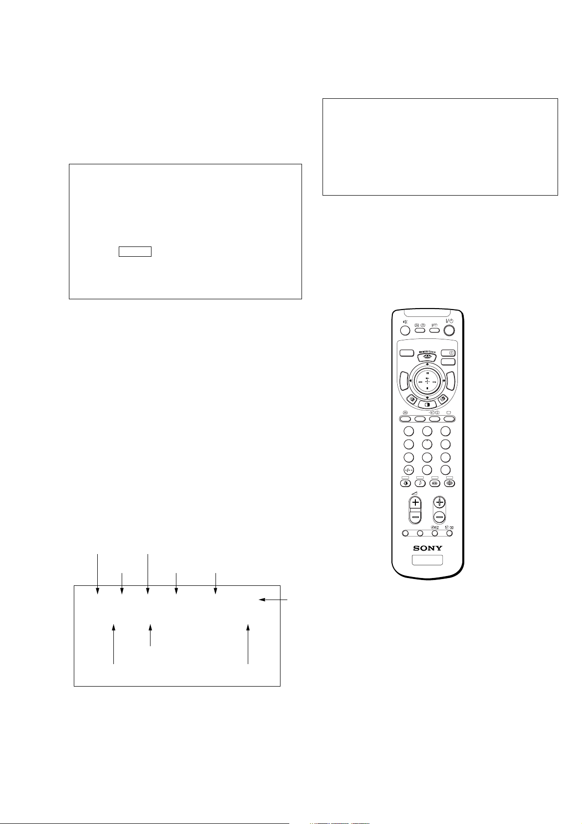
3-1. ADJUSTMENTS WITH COMMANDER
Service adjustments are made with the RM-951 that comes with
this unit.
a. ENTERING SERVICE MODE
With the unit on standby
↓
[DISPLAY]
↓
5
↓
VOL (+)
↓
[POWER]
This operation sequence puts the unit into service mode.
b. METHOD OF CANCELLATION FROM SERVICE
MODE
Set the standby condition (Press [POWER] button on the commander),
then press [POWER] button again, hereupon it becomes TV mode.
c. METHOD OF WRITE INTO MEMORY
1) Set to Service Mode.
2) Press [1] (UP) and [4] (DOWN), select an item of adjustment.
3) Press [MUTING] button and it will indicate WRITE on the screen.
4) Press [0] button to write into memory.
d. MEMORY WRITE CONFIRMATION METHOD
1) After adjustment, pull out the plug from AC outlet, and then
plug into AC outlet again.
2) Turn the power switch ON and set to Service Mode.
3) Call the adjusted items again to confirm adjustments were made.
1, 4 Select the adjustment item.
↓
3, 6 Raise/lower the data value.
↓
[MUTING] Writes.
↓
- Executes the writing.
7, - All the data becomes the values in memory.
8, - All user control goes to the standard state.
5, - Service data initialization (Be sure not to use
usually.)
[DISPLAY], - Write 50Hz adjustment data to 60Hz, or vice
versa.
2, - Write 50Hz adjustment data to 60Hz, or vice
versa.
VIDEO
DRC-MF
INDEX
PROG
123
456
7809
A/B
V CENTER
MENU
HD/DVD
JUMP
PROG
The screen display is :
Item No
00
Item Name
VPS 1C SERVICE
2. 4M
Device Name
GE1
Suffix No (OEM Code)
Data
00 00B5FF601S0
Software version
Total Power-On time (hours)
Mode
50
OPTION RESET
TV
PAL, SECAM : 50
NTSC : 60
RM-997
– 20 –
KV-HS29M61/M90/M91, HS34M61/M90/M91, HS38M61/M90/M91
RM-997
3-2. ADJUSTMENT METHOD
Item Number 00 of device GEO
This explanation uses H-Position as an example.
1. Select “GEO 00 HPS” with the 1 and 4 buttons.
2. Raise/lower the data with the 3 and 6 buttons.
3. Select the optimum state. (The standard is 1F for PAL reception.)
4. Write with the
WRITE.)
5. Execute the writing with the - button. (The WRITE
display will be changed to red color while excuting, and back
to SERVICE.)
GEO 00
F01Q0
[MUTING] button. (The display changes to
1C SERVICE 50VPS
FF00 00B52. 4M
GREEN
Adjusted with [3]
and [6] buttons.
Use the same method for all Items. Use 1 and 4 to select the
adjustment item, use 3 and 6 to adjust, write with
[MUTING],
then execute the write with -.
Note : 1. In
[WRITE], the data for all items are written into memory
together.
2. For adjustment items that have different standard data
between 50Hz or 60Hz, be sure to use the respective
input signal after adjustment.
GEO 00
F01Q0
GEO 00
F01Q0
1C SERVICE 50VPS
FF00 00B52. 4M
Written with [MUTING]
1C SERVICE 50VPS
FF00 00B52. 4M
Write executed with [0]
GREEN
RED
The WRITE display
then the display
returns to a green
SERVICE.
– 21 –
Adjustment Item Ta ble
Category Item Function Standard Data Device Name
No. Name PR50NC 100VC R450VC PR50VC TW50 IX50 HD1080i/50 120NC R460NC PR60NC 120VC R460VC PR60VC TW60 IX60 HD1080i/60 (Slave Address)
100NC R450NC PR50NC 100VC R450VC PR50VC TW50 IX50 HD1080i/50 120NC R460NC PR60NC 120VC R460VC PR60VC TW60 IX60 HD1080i/60 MS-MODE
GE1 00 VPS VERTICAL POSITION 19 19 19 19 19 19 19 19 19 1A 19 19 1A 19 19 19 19 19 19 CXA2170AQ(86H)
01 VSZ VERTICAL SIZE 26 28 28 26 28 28 28 28 28 25 29 29 28 27 29 29 29 29 29
02 VZO V SIZE OFF SET (PJ only) 00 0 00 00 00 00 00 00 00 00 00 00 00 00 00 00 00 00 00
03 VLN VERTICAL LINEARITY 07 7 07 07 07 07 07 07 07 06 07 07 06 07 07 07 07 07 07
04 VSC VERTICAL S CORRECTION 08 8 08 08 08 08 08 08 08 08 08 08 08 08 08 08 08 08 08
05 VCN VERTICAL CENTERING 1A 1A 1A 1A 1A 1A 1A 1A 1A 1A 1A 1A 1A 1A 1A 1A 1A 1A 1A
06 VPN VERTICAL PIN 12 12 12 12 12 12 12 12 12 12 12 12 12 12 12 12 12 12 12
07 MVP VERTICAL MIDDLE PIN 00 00 00 00 00 00 00 00 00 00 00 00 00 00 00 00 00 00 00
08 HTZ HORIZONTAL TRAPEZOID 00 00 00 00 00 00 00 00 00 00 00 00 00 00 00 00 00 00 00
09 MHZ MIDDLE HORIZONTAL TRAPEZOID 00 00 00 00 00 00 00 00 00 00 00 00 00 00 00 00 00 00 00
0A ZOM ZOOM SW 00 00 00 00 00 00 00 00 00 00 00 00 00 00 00 00 00 00 00
0B ASP ASPECT SWITCH 01 01 01 01 01 01 01 01 01 01 01 01 01 01 01 00 01 00 00
0C VSP ASPECT RATIO 2F 2F 2F 2C 2C 2C 2F 2F 38 2F 2F 2F 2D 30 2F 2F 2F 2D 2F
0D VSR VERTICAL SCROLL 1F 1F 1F 26 21 21 1F 1F 1F 1F 1F 1F 24 20 20 1F 1F 1E 21
0E UVL UPPER VERTICAL LINEARITY 00 0 00 00 00 00 00 00 00 00 00 00 00 00 00 00 00 00 00
0F LVL LOWER VERTICAL LINEARITY 00 0 00 00 00 00 00 00 00 00 00 00 00 00 00 00 00 00 00
GE2 00 HCT HORIZONTAL CENTERING 2D 2D 2D 2D 2D 2D 2D 2D 2D 2D 2D 2D 2D 2D 2D 2D 2D 2D 2D CXA2170AQ(86H)
01 HPS HORIZONTAL POSITION 15 15 15 15 15 15 15 15 15 13 13 13 13 13 13 13 13 13 13
02 HSZ HORIZONTAL SIZE 2D 2D 2D 2D 2D 2D 2D 2D 2D 2B 2B 2B 2B 2B 2B 2B 2B 2B 2B
03 SLN HORIZONTAL S CORRECTION 09 09 09 09 09 09 09 09 09 08 08 08 08 08 08 08 08 08 08
04 MPN HORIZONTAL MIDDLE PIN 06 06 06 06 06 06 06 06 06 05 05 05 05 05 05 05 05 05 05
05 PIN HORIZONTAL PIN 12 12 12 12 12 12 12 12 12 12 11 11 11 11 11 11 10 11 11
06 PN0 PIN OFF SET (PJ only) 00 00 00 00 00 00 00 00 00 00 00 00 00 00 00 00 00 00 00
07 UCP UPPER CORNER PIN 21 21 21 22 22 22 21 21 21 20 20 20 20 21 21 20 20 20 21
08 LCP LOWER CORNER PIN 23 23 23 24 25 25 23 23 23 22 22 22 21 23 23 22 22 22 22
09 UXG UPPER EXTRA CORNER PIN GAIN 00 00 00 00 00 00 00 00 00 00 00 00 00 00 00 00 00 00 01
0A LXG LOWER EXTRA CORNER PIN GAIN 00 00 00 00 00 00 00 00 00 02 00 00 00 00 00 00 00 00 00
0B UXP UPPER EXTRA CORNER PIN POSITION 00 0 00 00 00 00 00 00 00 00 00 00 00 00 00 00 00 00 03
0C UCP LOWER EXTRA CORNER PIN POSITION 00 0 00 00 00 00 00 00 00 03 00 00 00 00 00 00 00 00 00
0D LCP EXTRA CORNER PIN POLARITY 00 0 00 00 00 00 00 00 00 01 00 00 00 00 00 00 00 00 01
0E PPH PIN PHASE 15 15 15 15 15 15 15 15 14 16 14 14 16 16 16 14 14 14 17
0F VAG AFC ANGLE 1B 1B 1B 1B 1B 1B 1B 1B 1B 1D 1D 1D 1D 1D 1D 1D 1D 1D 1E
10 LNA LINEARITY ANGLE 21 21 21 21 21 21 21 21 21 1A 1A 1A 1A 1A 1A 1A 1A 1A 1C
11 VBW AFC BOW 1A 1A 1A 1A 1A 1A 1A 1A 1A 1C 1A 1A 1C 1A 1A 1A 1B 1C 1D
12 LBW LINEARITY BOW 29 26 26 29 26 26 26 26 26 26 26 26 26 26 26 26 26 26 26
– 22 –
KV-HS29M61/M90/M91, HS34M61/M90/M91, HS38M61/M90/M91
RM-997
– 23 –
Category Item Function Standard Data Device Name
No. Name PR50NC 100VC R450VC PR50VC TW50 IX50 HD1080i/50 120NC R460NC PR60NC 120VC R460VC PR60VC TW60 IX60 HD1080i/60 (Slave Address)
100NC R450NC PR50NC 100VC R450VC PR50VC TW50 IX50 HD1080i/50 120NC R460NC PR60NC 120VC R460VC PR60VC TW60 IX60 HD1080i/60 MS-MODE
GE3 00 HBL HORIZONTAL BLANKING SWITCH 01 1 01 01 01 01 01 01 01 01 01 01 01 01 01 01 01 01 01 CXA2170AQ(86H)
01 LBL LEFT BLANKING 36 36 36 36 36 36 36 36 36 36 36 36 36 36 36 36 36 36 36
02 RBL RIGHT BLANKING 1E 1E 1E 1E 1E 1E 1E 1E 1E 1E 1E 1E 1E 1E 1E 1E 1E 1E 1E
03 VBL VERTICAL BLANKING SWITCH 01 1 01 01 01 01 01 01 01 01 01 01 01 01 01 01 01 01 01
04 TBL TOP BLANKING 04 4 04 0F 0F 0F 04 04 0F 02 02 02 0F 0A 0A 02 02 08 02
05 BBL BOTTOM BLANKING 0A A 0A 0F 0F 0F 0A 0A 0F 06 06 06 0F 0F 0F 06 06 0F 06
06 BLK BLANKING OFF 00 0 00000000 00 00 00 000000000000000000 00
07 VCM VERTICAL COMPENSATION 00 0 00000000 00 00 00 000000000000000000 00
08 HCM HORIZONTAL COMPENSATION 00 0 00000000 00 00 00 000000000000000000 00
09 ACM AFC COMPENSATION 00 0 00000000 00 00 00 000000000000000000 00
0A PCM PIN COMPENSATION 00 0 00000000 00 00 00 000000000000000000 00
0B AFC AFC LOOP GAIN 01 1 01010101 01 01 01 010101010101010101 01
0C JMP REFERENCE PULSE JUMP SWITCH 00 0 00000000 00 00 00 000000000000000000 00
0D VSW VERTICAL DRIVE JUMP SWITCH 00 0 00000000 00 00 00 000000000000000000 00
0E RST VERTICAL DRIVE START SWITCH 00 0 00000000 00 00 00 000000000000000000 00
0F EWD PIN DC LEVEL SHIFT 00 0 00000000 00 00 00 000000000000000000 00
10 AKT AKB TIMING 15 15 15 1A 15 15 15 15 1F 14 14 14 16 14 14 14 14 10 14
11 PPL PIN COMP POLARITY 00 0 00000000 00 00 00 000000000000000000 00
12 M15 FH=15K @ MS MODE 00 0 00000000 00 00 00 000000000000000000 00
13 HFQ Fh setting @multi-scan 00 0 00 000000 00 00 00 000000000000000000 00
14 HFX Reciprocal Fh @mult-scan 00 0 00000000 00 00 00 000000000000000000 00
15 VMP VERTICAL MULTI-SCAN MODE 00 0 00000000 00 00 00 000000000000000000 00
16 ITL FREERUN INTERLACE SETTING 00 0 00000000 00 00 00 000000000000000000 00
17 VLL VERTICAL # OF LINE(L) 00 0 00000000 00 00 00 000000000000000000 00
18 VLH VERTICAL # OF LINE(H) 00 0 00000000 00 00 00 000000000000000000 00
19 AGC AGC SW for PAL 00 0 00000000 00 00 00 000000000000000000 00
Category Functionalit
y
Function Standard Data Device Name
No. Name RGBJ Deflection Table (Slave Address)
Common SD50NC/100NC/TW50/IX50 SD50VC/FF100VC HD1080i/50 SD60NC/SD120NC/TW60/IX60 SD60VC/120VC HD1080i/60 MS-MODE
GE4 00 DFS DF SW 00 CXA1875AM(46H)
01 DFH DF Phase 10 10 10 10 10 10 10 CXA1875AM(46H)
02 QPH QP Phase 1F 1F 1F 1F 1F 1F 1F CXA1875AM(46H)
03 QAM DQP AMPLITUDE 27 27 27 27 27 27 27 CXA2170(86H)
04 QAV DQP AMPLITUDE VERTICAL MODULATION 25 25 25 25 25 25 25 CXA2170(86H)
05 QAA DQP AMPLITUDE TILT 08 08 08 08 08 08 08 CXA2170(86H)
06 QPC DQP DC LEVEL 1C 1C 1C 1C 1C 1C 1C CXA2170(86H)
07 QPV DQP DC LEVEL VERTICAL MODULATION 27 36 37 27 36 37 27 CXA2170(86H)
08 QPP DQP DC LEVEL TILT 08 05 05 08 05 05 08 CXA2170(86H)
09 HTR Horizontal Trapezium 1F 1F 1F 1F 1F 1F 1F CXA1875AM(46H)
0A ROT Rotation 1F CXA1875AM(46H)
0B PCD Pin Correction Division Ratio 2 CXA2170(86H)
0C CPY COPY FUNCTION
KV-HS29M61/M90/M91, HS34M61/M90/M91, HS38M61/M90/M91
RM-997
Category Item Function Standard Data Device Name
Category Functionalit
y
Function Standard Data Device Name
No. Name Common Field Freq Multi Picture M
o
ABL Control Table (Slave Address)
50 60 MS-MODE Twin Index EcoOff VC EcoOff TW/IX EcoOff WD-N EcoOff Others EcoON VC EcoON TW/IX EcoON WD-N EcoON Others
SAJ 00 PIC Picture Control CXA2170(86H)
01 BRT Brightness Control
02 COL Color Control
03 HUE Hue Control
04 SHP Sharpness Control
05 VML VM Level
06 DYC Dynamic Color on/off
07 WBS White Balance Offset Setting
08 RYR Color Matrix Specification 0D 08
09 RYB Color Matrix Specification 0F 09
0A GYR Color Matrix Specification 07 09
0B GYB Color Matrix Specification 04 06
0C GMS Gamma Shape Correction
0D GMR Gamma Red
0E GMG Gamma Green
0F GMB Gamma Blue
10 DCT DC Transmission Control
11 APL Auto Pedestal Level Control
12 ABM ABL Mode Control
13 ABT ABL Current detection Vth Control 04 08 - 00 0F 0B - 0B
14 CLO Color Offset
15 CLW Color Step Width to the Change of S/N 03
16 HUO Hue Offset
17 SHO Sharpness Offset
18 SHW Sharpness Step Width to the Change of S/N 01
19 PIO Picture Offset for TWIN/INDEX/MS 07 07 07
1A BRO Brightness Offset for MS
1B DPL APED BLACK SIZE INFLECTED SETTING 00
1C TCO COLOR ON/OFF SETTING 00
No. Name Common Input Mode Table Group 2 (Slave Address)
Others (YUV) SD-I (YUV) SD-P (YUV) HD (RGB) SD-I (RGB) SD-P (RGB) HD MS
WHB 00 YOS DC Offset Canceller for Y Signal 07 CXA2170(86H)
01 UOS DC Offset Canceller for Cb Signal 1F 1F 28 2C 22 29 2D 1F
02 VOS DC Offset Canceller for Cr Signal 1F 24 2B 2D 21 28 2C 1F
03 SBR Sub Brightness Control 11
04 RDR R Drive 1F
05 GDR G Drive 1D
06 BDR B Drive 21
07 RCT R Cutoff 1F
08 GCT G Cutoff 1A
09 BCT B Cutoff 15
0A SBO Sub Brightness Offset 1F
0B RDO R Drive Offset 1F
0C GDO G Drive Offset 1C
0D BDO B Drive Offset 1B
0E RCO R Cutoff Offset 1F
0F GCO G Cutoff Offset 1B
10 BCO B Cutoff Offset 19
– 24 –
KV-HS29M61/M90/M91, HS34M61/M90/M91, HS38M61/M90/M91
RM-997
KV-HS29M61/M90/M91, HS34M61/M90/M91, HS38M61/M90/M91
Category Item Function Standard Data Device Name
No. Name NC VC (Slave Address)
DCN 00 SHS DC AMP3 1F 1F CXA8070P(DEh)
01 YBU VCA9 1F 1F
02 YBL VCA10 1F 1F
03 RAP DC AMP2 19 19
04 RUB VCA5 15 15
05 RLB VCA6 15 15
06 LAP DC AMP1 19 19
07 LUB VCA1 15 15
08 LLB VCA2 15 15
09 CAJ DC AMP4 1B 1B
0A RUM RIGHT UPPER MIDDLE BOW 1F 1F
0B RLM RIGHT LOWER MIDDLE BOW 1F 1F
0C LUM LEFT H AMP 1F 1F
0D LLM LEFT UPPER MIDDLE BOW 1F 1F
0E CPY Copy the DAC data to all vc/nc NVM area 0<-
CATEGIRY Item Function Standard Data Device Name
No. Name Picture/Sound Mode Table Input Mode Table Group 2
Dynamic Standard/Drama Hi-Fine/Soft Personal Others (YUV) SD-I (YUV) SD-P (YUV) HD (RGB) SD-I (RGB) SD-P (RGB) HD TV 50 Video 50 TV 60 Video 60 MS (Slave Address)
SAJ 00 PIC Picture Control 3F 32 25 CXA2170(86H)
01 BRT Brightness Control 21 1E 1F
02 COL Color Control 31 2A 21
03 HUE Hue Control 1F 1F 1F
04 SHP Sharpness Control 22 1F 1F
05 VML VM Level 0F 0A 05 0A
06 DYC Dynamic Color on/off 01 01 00 01
07 WBS White Balance Offset Setting 00 00 00 00
08 RYR Color Matrix Specification
09 RYB Color Matrix Specification
0A GYR Color Matrix Specification
0B GYB Color Matrix Specification
0C GMS Gamma Shape Correction 07 07 00 07
0D GMR Gamma Red 0A 03 00 03
0E GMG Gamma Green 0A 03 00 03
0F GMB Gamma Blue 0A 03 00 03
10 DCT DC Transmission Control 0A 03 00 03
11 APL Auto Pedestal Level Control 01 02 00 02
12 ABM ABL Mode Control 01 01 00 01
13 ABT ABL Current detection Vth Control
14 CLO Color Offset 0A 07 07 0A 07 07 03 09 07 07 00
15 CLW Color Step Width to the Change of S/N
16 HUO Hue Offset 06 07 07 07 07 07 05 04 07 07 07
17 SHO Sharpness Offset 07 0F 13 07 0F 13 0F 0F 0F 0F 0F
18 SHW Sharpness Step Width to the Change of S/N
19 PIO Picture Offset for TWIN/INDEX/MS
1A BRO Brightness Offset for MS 0F 0F 06 04 0F 06 04 07
1B DPL APED BLACK SIZE INFLECTED SETTING
1C TCO COLOR ON/OFF SETTING
– 25 –
RM-997
KV-HS29M61/M90/M91, HS34M61/M90/M91, HS38M61/M90/M91
Category Item Function Standard Data Device Name
No. Name Common (Slave Address)
LDG 00 NSC NS Correction 7F CXA1875AM(42H)
01 EWC EW Correction 7F
02 LX Left Cross Correction 7F
03 RX Right Cross Correction 7F
04 HST H Shift Correction 7F
05 ENS Environmental SW 0
06 TES Temperature SW 1
07 NSS NS SW 1
08 EWS EW SW 1
09 NSG NS Correction Gain 29 CXA2026AS(8eh)
0A EWG EW Correction Gain 24
0B ENG Environmental Correction Gain 3F
0C ENN NS Correction by Environment 0E
0D TLD Temp. Corr. DC of Left side 0F
0E TLU Temp. Corr. Gain of Left Upper 1F
0F TLL Temp.Corr. Gain of Left Lower 1F
10 TRD Temp. Corr. DC of Right side 0F
11 TRU Temp. Corr. Gain of Right Upper 1F
12 TRL Temp. Corr. Gain of Right Lower 1F
13 DHM DH Mute 0
14 DYP DY-Phase 7F CXA1875(46h)
15 LCL LCC Correction Limiter 3 CXA1875AM(42H)
Category Item Function Standard Data Device Name
No. Name Common Dynamic Standard/Drama Hi-Fine/Soft Personal Picture/Sound Mode Table (Slave Address)
(YUV) SD-I (YUV) SD-P (YUV) HD (RGB) SD-I (RGB) SD-P (RGB) HD TV 50 Video 50 TV 60 Video 60 MS
JGL 00 01 CXA2170(86H)
01 07
02 00
03 02
04 00
05 0A 0A 0A 0A 0A 0A 05 05 05 05 03
06 05
07 01 02 03 01 02 03 01 01 01 01 03
08 01 01 01 01 01 01 01 01 01 01 01 01
09 01 01 03 01 01 03 00 01 00 01 03
0A 03 03 03 03 03 03 03 03 03 03 03
0B 02 02 00 02
0C 01
0D 03 01 00 01
0E 07 07 07 07 07 07 07 07 07 07 07
0F 00 00 00 00 00 00 02 02 02 02 00
10 02 02 02 02 02 02 02 02 02 02 02
11 03 03 00 03 03 00 03 03 03 03 00
12 00
13 03
14 00
15 00
16 00
17 03
18 01 01 01 01 01 01 01 01 01 01 00
19 03
1A 00
1B 00
1C 0C
PON
RGB and AKB Reference Pulse Output On/Off
RGB
RGB Output Selection
AGG
Aging Mode Selection
BBT
RGB Bottom Limitter Control
LML
RGB Amplitude Limitter Control
SCO
Sub Picture Control
LEV
RGB Level for RGB
SYS
Signal Band Selection
SF0
Sharpness f0 setting
SF1
High f0 sharpness gain control
PRO
Pre/Over-Shoot Ratio Control
LTI
Luminance Transient Improvement
LTM
LTI Mode Setting
CTI
Chrominance Transient Improvement
VDL
VM OUT Phase Control
VCR
VM OUT Coring Level Setting
VFO
VM OUT F0 Setting
VLM
VM OUT Limiter Level Setting
SPH
H Sync Delay Timing Setting
CLP
CLP Pulse Phase Control
CLG
CLP Pulse Gate Setting
CLS
CLP Pulse Start Phase Setting
YOS
DC_OFFSET RANGE FOR Y SIGNAL SETTING
YLT
Y AMPLITUDE LIMITER LEVEL SETTING
YCS
Y SIGNAL GAIN SETTING
PHA
PHASE ADJ
AKO
AKB_OFF
HBS
RGB OUTPUT H BLANKING WHEN AKBOFF=0
ARG
AUTO REGI LRGB_LEV
– 26 –
RM-997
Category Item Function Standard Data Device Name
No. Name Common Input Mode Table Group 1 (Slave Address)
2DComb 3DComb S-Input others TV Video DVD 50TV 50Video 50DVD 60TV 60Video 60DVD
YCT 00 TNT Tint Adjustment for NTSC 1F 1F CXA2163Q(88H)
01 PNG PAL/NTSC Gate Width 01
02 PNI PAL/NTSC Sensitivity SW 00
03 SCL Sub Color Control 07 07 07 07
04 SCT Sub Contrast Control 07 07 07 07
05 SF0 Sharpness Center Frequency Changing 02
06 SEQ Sharpness Equalizer Characteristic 03
07 SHG Sharpness Gain Control 04 04 04 04 04 04
08 YOL Y-output Level Control 22
09 BSP Black Stretch Start Point Changing 00
0A COL Cb/Cr Output Level Control 1D
0B DCR DC Restoration Ratio Adjustment 00
0C BF0 BPF/TQF F0 Adjustment 00
0D BFQ BPF/TQF Q Adjustment 02
0E FSW BPF/TQF Switch 01
0F SDT SECAM Double Trap Switch 01
10 LPF Y/Cb/Cr LPF Switch 01
11 YDL Y-DL Time Adjustment 06 05 03 05
12 B01 Cb Offset1 Adjustment (main route) 09
13 RO1 Cr Offset1 Adjustment 06
14 CDF V Count Down Frequency Switch 00
15 CDM V Count Down Judge Switch 00
16 AFC AFC Sensitivity Switch 00 00
17 MVM Macrovision Mask + AFC Mask 00
18 SRY SECAM R-Y Black Adjustment 07
19 SBY SECAM B-Y Black Adjustment 01
1A BEL SECAM BELL/HPF Switching 02
1B BLF BELL f0 Adjustment 00
1C SVI SECAM V-ID Switch 00
1D SGP SECAM Gate Position Adjustment 00
1E SID SECAM Sensitivity Switch 01
1F SIH SECAM Inhibition Switch 00
20 STP Y Black Level Setup for PAL plus 00
21 ASW AUTO SWITCH 01
22 3NR 3D NR Operation on/off 01
23 BW6 3D NR for 60Hz non-bust signal on/off 01
24 WSH Sharpness Gain Step for noise reduction 00
25 WCO Cb/Cr Output Level Step for noise reduction 00
– 27 –
KV-HS29M61/M90/M91, HS34M61/M90/M91, HS38M61/M90/M91
RM-997
Category Functionalit
y
Category
y
Function Standard Data
No. Name Common HD/DVD Input Table Device Name
fh15k otherfh RGB HD720p/1080i DVD (Slave Address)
SYN 00 MAT Matrix Conversion 03 01 00 CXA2171(8CH)
01 VFR Dummy Sync Freq 01
02 SL1 Input Signal Type for IN1 00
03 SL2 Input Signal Type for IN2 01
04 FSY Sync Identification Mode 01 03 03
05 VTC V sync Separation Time Constant 03 00
06 HWD Output Pulse Width 01 00
07 HSL Sync Separation Mode 01
08 HTC H-Sync Separation Time Constant 01 01
09 HSW YG Out signal Output 00
0A HMA Hsync within V sync 00
0B MAC Macrovision 01
0C DUM Out dummy sync or signal sync 00
0D CLK Clock Select 00
0E GSL Gain Select 00
0F CBG CB Gain 07
10 CRG CR Gain 07
11 YG Y Gain 07
12 HFR Dummy Frequency Select 01
– 28 –
No. Name Common S-Input SECAM NTSC PAL TV Video DVD 50TV 50Video 60TV 60Video (Slave Address)
SYC 00 TNT Tint Adjustment for NTSC 1F 1F CXA2163Q(8AH)
01 PNG PAL/NTSC Gate Width 01
02 PNI PAL/NTSC Sensitivity SW 00
03 SCL Sub Color Control 07 07 07 07
04 SCT Sub Contrast Control 07 07 07 07
05 SF0 Sharpness Center Frequency Changing 02
06 SEQ Sharpness Equalizer Characteristic 03
07 SHG Sharpness Gain Control 07
08 YOL Y-output Level Control 19
09 BSP Black Stretch Start Point Changing 00
0A COL Cb/Cr Output Level Control 13
0B DCR DC Restoration Ratio Adjustment 00
0C BF0 BPF/TQF F0 Adjustment 01
0D BFQ BPF/TQF Q Adjustment 02
0E FSW BPF/TQF Switch 01
0F SDT SECAM Double Trap Switch 01
10 LPF Y/Cb/Cr LPF Switch 01
11 YDL Y-DL Time Adjustment 05 03 03 03
12 NCM 1-H Addition Switch 01
13 B01 Cb Offset1 Adjustment (main route) 09
14 RO1 Cr Offset1 Adjustment 09
15 CDF V Count Down Frequency Switch 00
16 CDM V Count Down Judge Switch 00
17 AFC AFC Sensitivity Switch 00 00
18 MVM Macrovision Mask + AFC Mask 00
19 SRY SECAM R-Y Black Adjustment 07
1A SBY SECAM B-Y Black Adjustment 01
1B BEL SECAM BELL/HPF Switching 02
1C BLF BELL f0 Adjustment 00
1D SVI SECAM V-ID Switch 00
1E SGP SECAM Gate Position Adjustment 00
1F SID SECAM Sensitivity Switch 01
20 SIH SECAM Inhibition Switch 00
21 STP Y Black Level Setup for PAL plus 00
22 ASW SUB AUTO SWITCH 01
Function Stamdard Data Device Name
KV-HS29M61/M90/M91, HS34M61/M90/M91, HS38M61/M90/M91
Functionalit
RM-997
KV-HS29M61/M90/M91, HS34M61/M90/M91, HS38M61/M90/M91
Category Item Function Standard Data Device Name
No. Name Common BSW 0 Sound Mode Table BSW 1 Sound Mode Table (Slave Address)
Dynamic Drama Soft Personal Dynamic Drama Soft Personal
AP 00 0 NJW1139(82H)
01 0
02 0
03 0
04 3
05 0
06 0
07 10 11 13 10 11 13
08 14 14 14 14 14 14
09 A7 53 00 A7 53 00
MSP 00 15 MSP3415D(84H)
01 EC
02 05
03 01
04 30
05 20
06 10
07 01
08 28
09 00
0A 01
0B 1B
0C 32
0D 36
0E 65
0F 1C
10 7F
11 50
12 30
Bass Boost Setting
Boost/Cut Sub-Bass
Sub-Bass Setting
Boost/Cut Sub-Treble
Sub-Treble Setting
AGC Level Setting
Bass Boost Switch
W/G Stereo Threshold
W/G Bilingual Threshold
W/G Monaural Threshold
W/G Agreement Count
W/G Search Delay
NICAM Search Delay
Stereo status Read Delay
AGC Switch Auto/Constant
AGC Gain at Constant Mode
Carrier muting on/off
Audio Clock out on/off
FM Prescale for non-M system
FM Prescale for M system
FM Prescale for HDEV
FM Prescale for HDEV and M
W/G Prescale
NICAM Prescale
Auto FM switch Threshold
Loud Speaker gain 0700h to 07FFh
BBE Sound mode Control
Treble sound mode Control
Bass sound mode Control
BBS
BCB
SBS
BCT
STS
AGL
BSW
WST
WBT
WLL
WAC
WDL
NDL
SDL
AGC
REL
CRM
ACO
FP
FPM
FH
FHM
WGP
NIP
ERR
VOL
BBE
TRE
BAS
– 29 –
RM-997
Category Item Function Standard Data Device Name
– 30 –
No. Name Common Multi Picture Mode Picture/Sound Mode Table (Slave Address)
Twin TV Video Dynamic Standard/Drama Hi-Fine/Soft Personal
LTI 00 LDH Histogram segment Selection 01 TDA9178(40H)
01 CFS Contour Filter Selection 01
02 WLB Letterbox Window Switch 00
03 VDC Video Dependent Coring 01 01 01 01
04 DEM Demonstration Mode 00
05 CDP Luminance Delay 04
06 OSP Overrule Smart Peaking 00
07 WPO White Point Stretch Off 00
08 DSK Skin Tone Switch 00 00 00 00
09 ASK Skin Tone Angle Selection 00
0A WSK Skin Tone Width Selection 00
0B SSK Skin Tone Size selection 00
0C DGR Green Enhancement switch 00 01 01 00 01
0D DGT Threshold of Green Enhancement switch 07
0E GGR Green Enhancement Gain 00
0F WGR Green Enhancement Width 00
10 SGR Green Enhancement Size 00
11 DBL Blue Stretch Switch 00
12 GBL Blue Stretch Gain Selection 00
13 SBL Blue Stretch Size selection 00
14 CDS Color Dependent Sharpness 01 01 01 01
15 CST Threshold of Color Dependent Sharpness 07
16 CTI Color Transient Improvement 01 00 00 00
17 BON Black offset Compensation 00 00 00 00
18 BTD Adaptive Black Strecth 00 00 00 00
19 NLD Non-Linearity Amplifier 00 15 13 05 13
1A NLW Step Width of Non-Linearity Amplifier 04
1B VGD Variable Gamma 1F 1F 15 1A 15
1C VGW Step Width of Variable Gamma 00
1D PKD Peaking Amplitude 3F 2F 1D 2F
1E PKW Step Width of Peaking Amplitude 08
1F SPD Steepness Correction 00 00 00 00
20 CRD Coring Level 16 1B 0F 1B
21 CRW Step Width of Coring Level 09
22 CRO Coring Level Offset for Video Mode 09
23 LWD Line Width Correction 1F
24 SNM S/N Mode under unreliable S/N condition 01
25 SNC S/N Ratio Average Counter 03 03
26 FMC Feature Mode Matching Counter 02
KV-HS29M61/M90/M91, HS34M61/M90/M91, HS38M61/M90/M91
RM-997
 Loading...