

Page 1
REVISION HISTORY
BX1S
CHASSIS
MODEL
KV-AR14M80
NO. SUFFIX DATE SUPPL. / CORR DESCRIPTION
1 -01 2004/5 -- 1st. Issue
PART NO. : 9-872-450-01
Page 2
SERVICE MANUAL
BX1S
CHASSIS
MODEL COMMANDER DEST. CHASSIS NO.
KV-AR14M80
RM-W101 E SCC-U98R-A
MODEL COMMANDER DEST. CHASSIS NO.
RM-W101
TRINITRON
®
COLOR TV
Page 3

KV-AR14M80
RM-W101
TABLE OF CONTENTS
Section Title Page
SELF DIAGNOSTIC FUNCTION.............................. 3
1. DISASSEMBLY
1-1. Rear Cover Removal ................................................. 6
1-2. Speaker Removal ...................................................... 6
1-3. Chassis Assy Removal .............................................. 6
1-4. Service Position ........................................................ 6
1-5. Terminal Bracket Removal ....................................... 6
1-6. A Board Removal ...................................................... 6
1-7. Picture Tube Removal ............................................... 7
2. SET-UP ADJUSTMENTS
2-1. Beam Landing ........................................................... 8
2-2. Convergence .............................................................. 9
2-3. Focus Adjustment .................................................... 11
2-4. G2 (SCREEN) Adjustments ................................... 11
2-5 White Balance Adjustment ..................................... 11
2-6 Sub Bright Adjustment ........................................... 11
3. CIRCUIT ADJUSTMENTS
3-1. Adjustment With Commander ................................ 12
3-2. Adjustment Method ................................................ 13
3-3. Picture Quality Adjustment .................................... 26
3-4. Deflection Adjustment ............................................ 26
3-5. Drive Adjustment .................................................... 27
3-6. Picture Distortion Adjustment ................................ 28
Section Title Page
4. DIAGRAMS
4-1. Block Diagram ........................................................ 29
4-2. Circuit Boards Location .......................................... 30
4-3. Schematic Diagram Information ............................ 30
4-3-1. C Board Schematic Diagram ....................... 31
4-3-2. A Board — Processor (Block A) ................. 32
4-3-3. A Board — Audio (Block B) ....................... 34
4-3-4. A Board — Power Supply (Block C) .......... 36
4-3-5. A Board — Deflection (Block D)................ 38
4-3-6. A Board — Tuner (Block E) ........................ 40
4-3-7. A Board — Jack (Block F) .......................... 42
4-4. Voltage Measurement and Waveforms ................... 44
4-5. Printed Wiring Boards and Parts Location ............. 47
4-6. Semiconductors ....................................................... 50
5. EXPLODED VIEWS
5-1. Chassis ..................................................................... 52
6. ELECTRICAL PARTS LIST .................................... 53
OPERATING INSTRUCTIONS
CAUTION
SHORT CIRCUIT THE ANODE OF THE PICTURE TUBE AND
THE ANODE CAP TO THE METAL CHASSIS, CRT SHIELD,
OR CARBON PAINTED ON THE CRT, AFTER REMOVING THE
ANODE.
SAFETY-RELATED COMPONENT WARNING!!
COMPONENTS IDENTIFIED BY SHADING AND MARK ! ON
THE SCHEMATIC DIAGRAMS, EXPLODED VIEWS AND IN
THE PARTS LIST ARE CRITICAL TO SAFE OPERATION.
REPLACE THESE COMPONENTS WITH SONY PARTS
WHOSE PART NUMBERS APPEAR AS SHOWN IN THIS
MANUAL OR IN SUPPLEMENTS PUBLISHED BY SONY.
– 2 –
Page 4

KV-AR14M80
SELF DIAGNOSTIC FUNCTION
The units in this manual contain a self diagnostic function. If an error occurs, the STANDBY (1) indicator will automatically
begin to flash. A description of the self-diagnosis function is explained in the instruction manual. The number of times the
STANDBY (1) indicator flashes translates to a probable source of the problem. If an error symptom cannot be reproduced,
the remote commander can be used to review the failure occurrence data stored in memory to reveal past problems and
how often these problems occur.
1. DIAGNOSTIC TEST INDICATORS
When an errors occurs, the STANDBY (1) indicator will flash a set number of times to indicate the possible cause of the
problem. If there is more than one error, the indicator will identify the first of the problem areas.
Result for all of the following diagnosis items are displayed on screen. No error has occured if the screen displays a "0".
RM-W101
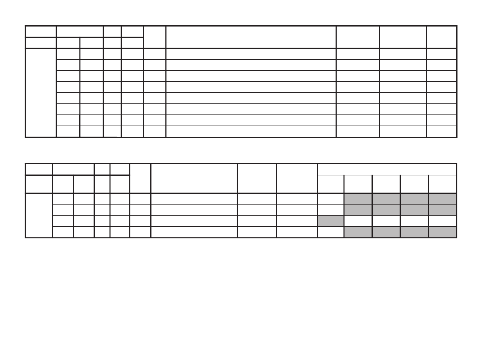
Diagnosis
Item
Description
Power does
not turn on
+B overcurrent
(OCP)*
V-Protect
IK (AKB)
Power supply
NG (+5V) for
Video Processor
* If a +B overcurrent is detected, stoppage of the vertical deflection is detected simultaneously. The symptom that is
diagnosed first by the micro controller is displayed on the screen.
** Refer to Screen (G2) Adjustment in this manual.
No. of timer
STANDBY (1)
indicator flashes
Does not light
2 times
4 times
5 times
8 times
Self-Diagnostic
display/
Diagnosis result
–
2:0
or
2:1 ~ 255
4:0
or
4:1 ~ 255
5:0
or
5:1 ~ 255
8:0
or
8:1 ~ 255
Probable Cause
Location
• Power cord is not plugged
in.
• Fuse is burned out (F600)
A board.
• H OUT (Q805) is shorted.
(A board)
• IC751 is shorted. (C board)
• +13V is not supplied.
(A board)
• IC804 is faulty. (A board)
• Video OUT (IC1545) is
faulty. (A board)
• IC001 is faulty. (A board)
• Screen (G2) is improperly
adjusted.**
• IC604 faulty.
• IC602 faulty.
Detected
Symptoms
• Power does not turn on.
• No power is supplied on
TV.
• AC Power supply is faulty.
• Power does not turn on.
• Load on power line is
shorted.
• Has entered standby state
after horizontal raster.
• Vertical deflection pulse is
stopped.
• Power line is shorted or
power supply is shorted.
• No raster is generated.
• CRT Cathode current
detection reference pulse
output is small.
• No power supply to CRT
ANODE.
• No RASTER is generated.
– 3 –
Page 5
KV-AR14M80
RM-W101
2. DISPLAY OF STANDBY (1) INDICATOR
FLASH COUNT
2 times
4 times
5 times
8 times
Lamp ON 300ms
Lamp OFF 300ms
Lamp OFF 3 sec.
Diagnostic Item Flash Count*
+B overcurrent 2 times
V-Protect 4 times
IK (AKB) 5 times
Power Supply NG (+5V) 8 times
for Video processor
* One flash count is not used for self-diagnosis.
STANDBY u indicator
3. STOPPING THE
STANDBY (1) INDICATOR FLASH
Turn off the power switch on the TV main unit or unplug the power cord from the outlet to stop the STANDBY (1)
indicator from flashing.
4. SELF-DIAGNOSTIC SCREEN DISPLAY
For errors with symptoms such as "power sometimes shuts off" or "screen sometimes goes off" that cannot be confirmed,
it is possible to bring up past occurrences of failure on the screen for confirmation.
[To Bring Up Screen Test]
In standby mode, press buttons on the remote commander sequentially in rapid succession as shown below:
Display
/ Channel 5 / Volume / Power / TV
˘
Note that this differs from entering the service mode (volume [+]).
The following screen will be displayed indicating the error count.
SELF DIAGNOSTIC
2 : 0
3 : N/A
4 : 0
5 : 1
8 : 0
101 : N/A
Numeral "0" means that no fault was detected.
Numeral "1" means the number of a fault occurrence (1 ~ 255).
– 4 –
Page 6
KV-AR14M80
5. HANDLING OF SELF-DIAGNOSTIC SCREEN DISPLAY
Since the diagnostic results displayed on the screen are not automatically cleared, always check the self-diagnostic
screen during repairs. When you have completed the repairs, clear the result display to "0".
Unless the result display is cleared to "0", the self-diagnosis function will not be able to detect subsequent faults after
completion of the repairs.
[Clearing the result display]
To clear the result display to "0", press buttons on the remote commander subsequent as shown below when the
self-diagnostic screen is being displayed.
8 , -
[Quitting Self-diagnostic screen]
To quit the entire self-diagnostic screen, turn off the power switch on the remote commander or the main unit.
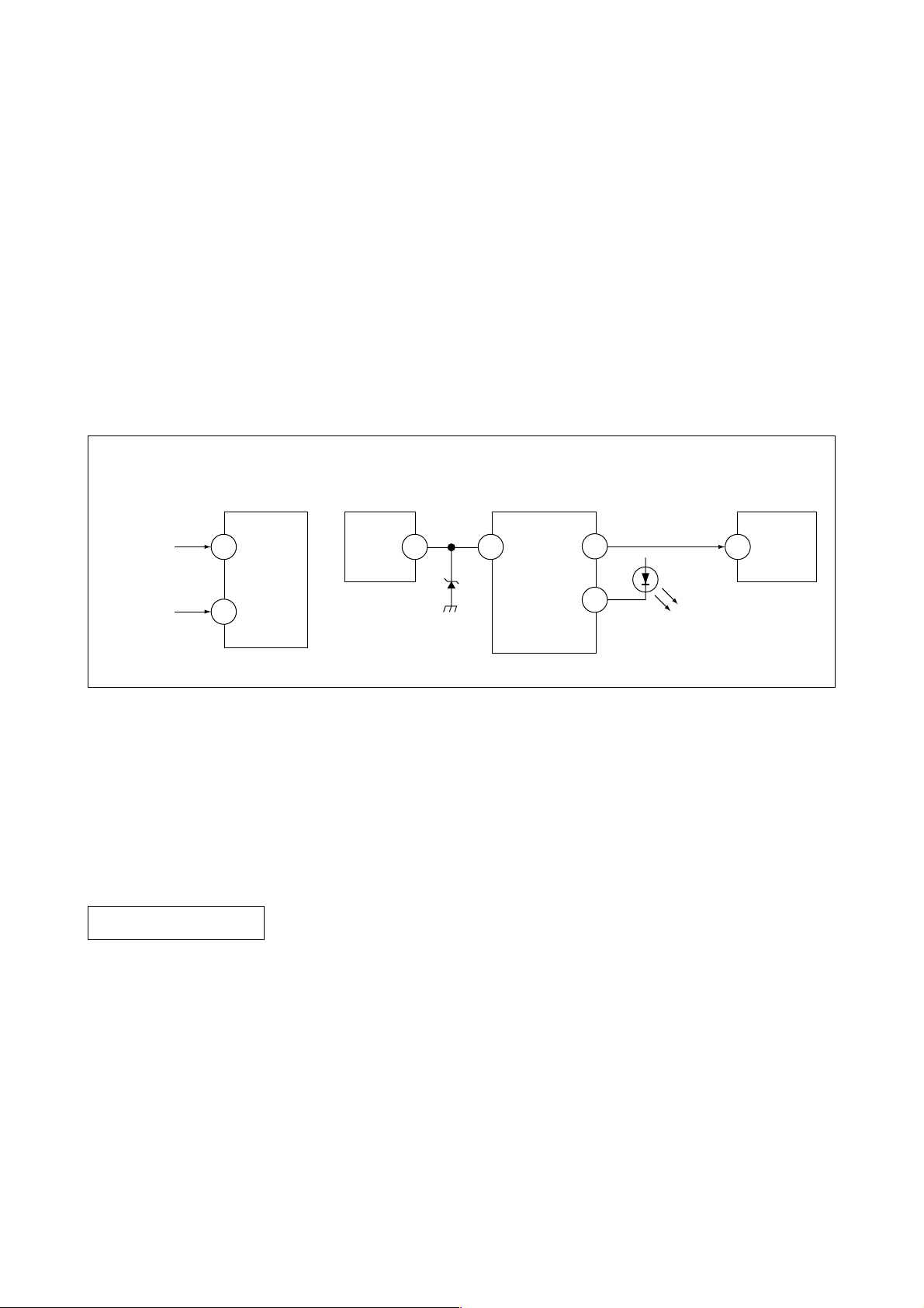
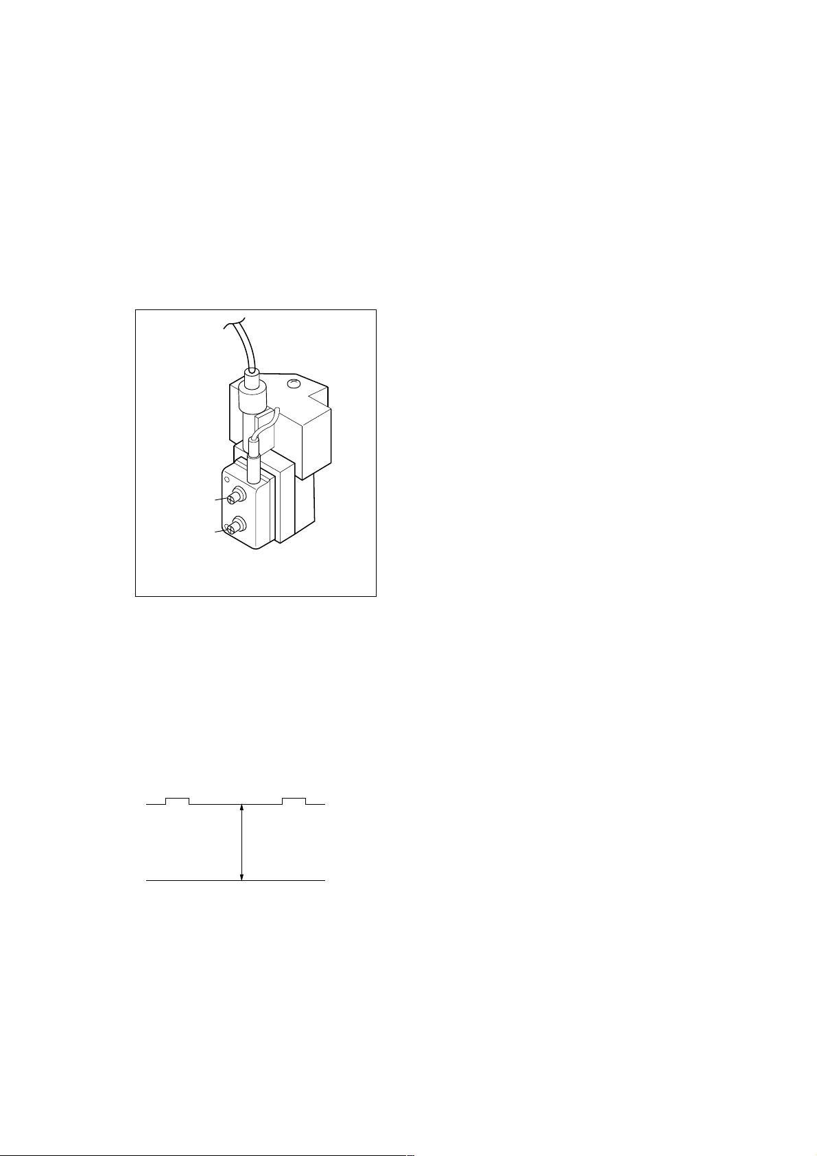
6. SELF-DIAGNOSTIC CIRCUIT
RM-W101
FROM
C BOARD
IC751 PIN 5
A BOARD
FROM
Q816
COLLECTOR
A BOARD
IC001
Y/CHROMA JUNGLE
IK
32
EHTO
A BOARD
IC804
V.OUT
F.B-PLS
A BOARD
IC001
SYSTEM
SDA1
3 1384
V.GUARD
RED LED
99
122
DISPLAY
A BOARD
IC003
MEMORY
5
SDA
[+B overcurrent $OCP%] Occurs when an overcurrent on the +B(135V) line is detected by pin 32 of IC001 (A board).
If the voltage of pin 32 of IC001 (A board) is more than 4V, the unit will automatically go
to standby.
[V-PROTECT] Occurs when an absence of the vertical deflection pulse is detected by pin 13 of IC001
(A board).
[IK $AKB%] If the RGB levels* do not balance within 15 sec after the power is turned on, this error will
be detected by IC001 (A board). TV will stay on, but there will be 5 times LED blinking.
POWER SUPPLY NG (+5V)
for VIDEO PROCESSOR
Occurs when IC001 internal HV protect detects an abnormal H-Pulse (frequency) due to
improper power supply to IC001. TV cuts off high voltage power of anode CRT. No picture
will be detected. eg: IC602, IC604 go faulty.
* (Refers to the RGB levels of the AKB detection Ref pulse that detects IK.)
– 5 –
Page 7
KV-AR14M80
RM-W101
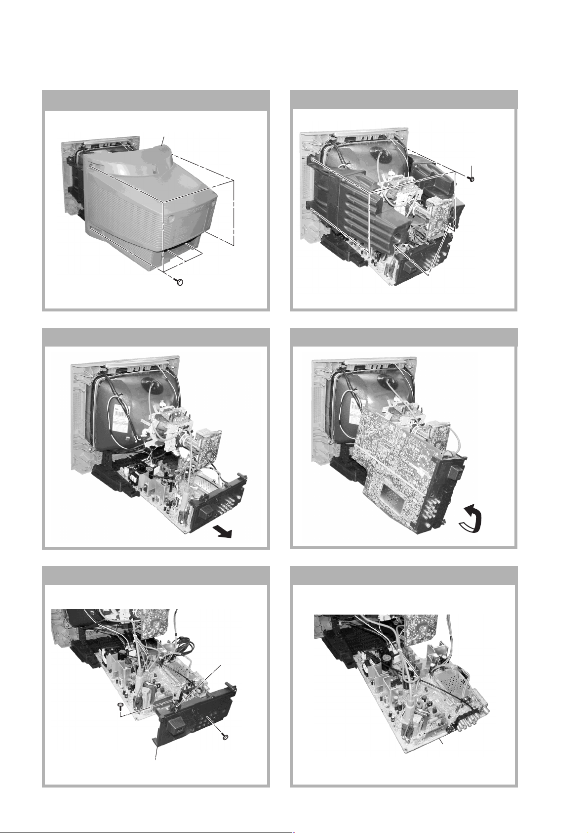
SECTION 1
DISASSEMBLY
1-1. REAR COVER REMOVAL
2 Rear cover
1 Six screws
(+BVTP 4 × 16)
1-2. SPEAKER REMOVAL
1-3. CHASSIS ASSY REMOVAL 1-4. SERVICE POSITION
1 Four screws
(Washer Head)
(+P4 × 16)
2 Speaker Block Assy
1-5. TERMINAL BRACKET REMOVAL 1-6. A BOARD REMOVAL
4 FBT
bracket
1 One screws
(+BVTP 3 × 12)
3 One screws
(+BVTP 4 × 16)
2 Terminal bracket
– 6 –
A Board
Page 8
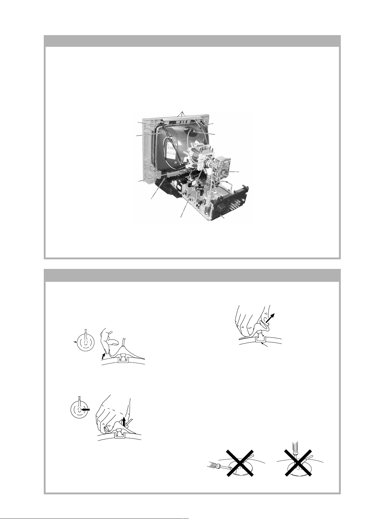
KV-AR14M80
1-7. PICTURE TUBE REMOVAL
Note:
• Please make sure the TV set is not in standing position before removing necessary CRT support located on bottom
right and left.
1) Place the TV set with the CRT face down on a cushion jig.
2) Remove the rear cover.
3) Unplug all inter connecting leads from the Deflection Yoke, Degaussing Coil and CRT grounding strap.
Top switch, block
qf
Nut, Special, CRT (x4)
qd
Degaussing Coil
0
Spring Tension Removal
qa
Earth Coating Assy
qs
Anode Cap Removal
4
5 C Board Removal
RM-W101
8 Support, CRT Removal (x2)
Loosen the Deflection Yoke
6
fixing screw and remove
7 Chassis Assy Removal
• REMOVAL OF ANODE-CAP
Note:
• After removing the anode, short circuit the anode of the picture tube and the anode cap to the metal chassis, CRT
shield or carbon paint on the CRT.
• REMOVING PROCEDURES
a
a
1 Turn up one side of the rubber cap in the direction
indicated by the arrow A.
b
b
Anode Button
turning up the rubber cap and pulling it up in the
direction of the arrow C.
• HOW TO HANDLE AN ANODE-CAP
1 Do not damage the surface of anode-caps with
sharp shaped objects.
2 Do not press the rubber too hard so as not to
damage the inside of anode-cap.
A metal fitting called the shatter-hook terminal is
built into the rubber.
3 Do not turn the foot of rubber over too hard.
The shatter-hook terminal will stick out or damage
the rubber.
c
2 Using a thumb pull up the rubber cap firmly in the di-
rection indicated by the arrow B.
3 When one side of the rubber cap is separated from
the anode button, the anode-cap can be removed by
– 7 –
Page 9
KV-AR14M80
Purity control
RM-W101
SECTION 2
SET-UP ADJUSTMENTS
• The following adjustments should be made when a
complete realignment is required or a new picture
tube is installed.
Perform the adjustments in the following order :
1. Beam Landing
2. Convergence
3. Focus
Set the controls as follows unless otherwise noted:
VIDEO model ..................................................... Standard
PICTURE control .................................................. normal
BRIGHTNESS control .......................................... normal
4. Screen(G2)
5. White Balance
Note : Test Equipment Required.
1. Pattern Generator
2. Degausser
3. DC Power Supply
4. Digital Multimeter
5. Oscilloscope
......................................................................................................................................................................................................................
Preparation :
• In order to reduce the influence of geomagnetism on
the set's picture tube, face it east or west.
• Switch on the set's power and degauss with the
degausser.
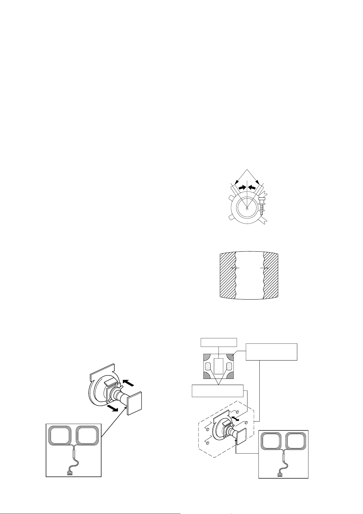
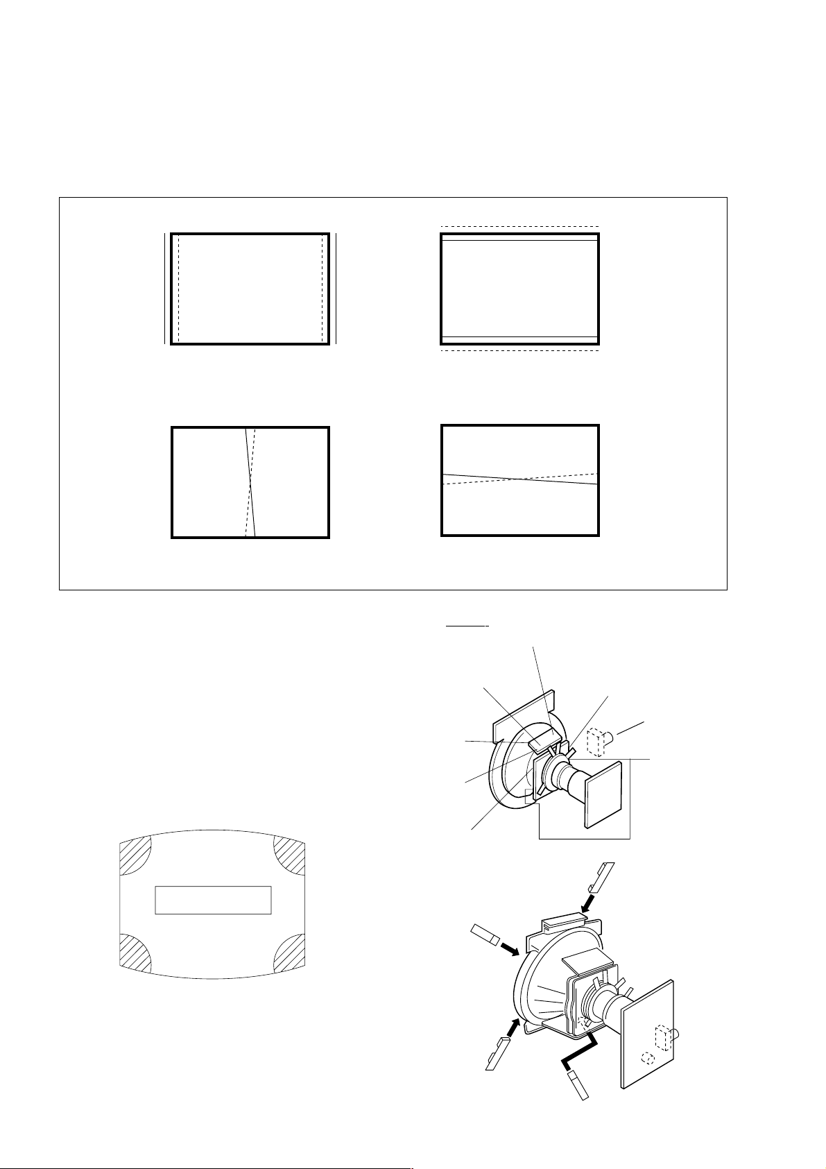
2-1. BEAM LANDING
Picture Mode: DYNAMIC
1. Input a white signal with the pattern generator.
Contrast
Brightness
}
normal
2. Set the pattern generator raster signal to a green
raster.
3. Move the deflection yoke to the rear and adjust with
purity control so that the green is at the center and
the blue and the red take up equally sized areas on
each side. (See Figures 2-1 through 2-4.)
4. Move the deflection yoke forward and adjust so that
the entire screen is green. (See Figure 2-1.)
5. Switch the raster signal to blue then to red and verify
the condition.
6. When the position of the deflection yoke has been
decided fasten the deflection yoke with the screws
and DY spacers.
7. If the beam does not land correctly in all the corners,
use a magnet to adjust it. (See Figure 2-4.)
Purity control
corrects this area.
b
a
Fig. 2-2
Blue
Red
Green
Fig. 2-3
Disk magnets or rotatable
disk magnets correct these
areas (a-d).
d
c
Deflection yoke positioning
corrects these areas.
b
c
a
d
Fig. 2-1 Fig. 2-4
– 8 –
Page 10
KV-AR14M80
RM-W101
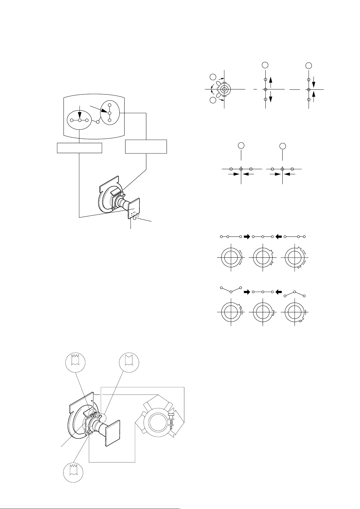
2-2. CONVERGENCE
• Before starting this adjustment, adjust the focus,
horizontal size and vertical size.
• Receive dot/hatch signal.
• Pic mode: Soft.
(1) Horizontal and Vertical Static Convergence
Center dot
R G B
H. STAT VR
R
G
B
V. STAT
Magnet
RV750
H. STAT
C Board
Operation of V.STAT magnet
If the V.Stat magnet is moved in the “A” and “B” arrows,
the red, green and blue dots moves as shown below.
A
B
A
B
G
R
B
B
G
R
Moved RV750 H.STAT.
the red, green and blue dots move as shown below.
A
RGGBB
B
R
4. BMC (Hexapole) Magnet.
If the red, green and blue dots are not balanced or
aligned, then use the BMC magnet to adjust in the
manner described below.
RG B R G B R GB
1. (Moving vertically), adjust the V.STAT magnet so that
the red, green and blue dots are on top of each other
at the center of the screen.
2. (Moving horizontally), adjust the H.STAT control so
that the red, green and blue dots are on top of each
other at the center of the screen.
3. If the H.STAT variable resistor cannot bring the red,
green and blue dots together at the center of the
screen, adjust the horizontal convergence with the
H.STAT variable resistor and the V.STAT magnet in
the manner given below.
(In this case, the H.STAT variable resistor and the
V.STAT magnet influence each other, so be sure to
perform adjustments while tracking.)
BMCPurity
BMC (Hexapole)
Purity
RB
G
RG
GB
RB
DY pocket
V.STAT
V.STAT
– 9 –
Page 11
KV-AR14M80
RM-W101
(2) Convergence Rough Adjustment
(2) Convergence Rough Adjustment
Preparation:
Preparation:
• Before starting this adjustment, adjust the horizontal
• Before starting this adjustment, adjust the horizontal
static convergence and the vertical static
static convergence and the vertical static
convergence
convergence
B
R
B
R
TLH
RB
YCH
TLH Insert TLH Correction Plate to DY Pocket
TLH Insert TLH Correction Plate to DY Pocket
(Left or Right)
(Left or Right)
YCH Insert YCH VOL on DY
YCH Insert YCH VOL on DY
TLV Rotate TLV VOL on DY
TLV Rotate TLV VOL on DY
XCV Rotate XCV Adj core on DY
XCV Rotate XCV Adj core on DY
(3) Screen corner Convergence
(3) Screen corner Convergence
1. Affix a Piece A (90), conv. correct corresponding to
1. Affix a Piece A (90), conv. correct corresponding to
the misconverged areas.
the misconverged areas.
R
B
ON DY:
TLV
XCV
YCH
TLV
XCV
TLV
DY pocket
TLH Plate
XCV
ba
a-d : screen-corner
misconvergence
cd
– 10 –
DY pocket
a
d
Piece A (90), conv. correct
b
c
Page 12
KV-AR14M80
RM-W101
2-3. FOCUS ADJUSTMENT
FOCUS adjustment should be completed before the W/B
adjustment:
1. Receive digital monoscope pattern.
2. Set picture mode: DYNAMIC.
3. Adjust focus VR to obtain a just focus at the center of
the screen.
4. Change receiving signal to white pattern and blue
back.
5. Confirm MAGENTA RING is not noticeable. Incase
magenta ring is obvious, then adjust FOCUS VR to
balance magenta ring and FOCUS.
FOCUS
SCREEN
2-5. WHITE BALANCE ADJUSTMENT
1. Set to Service Mode (Refer Section 3-1:
ADJUSTMENTS WITH COMMANDER)
2. Input white raster signal.
3. Set Picture to <DYNAMIC mode>
4. Select RDRV (02) with
to 25 with
3 and 6.
5. Adjust WHBL GDRV (03) and BDRV (04) with
4 and adjust the data with 3 and 6 for best white
1 and 4 and fixed the value
1 and
balance in Highlight condition.
6. Write into the memory by pressing [MUTING] then
7. Adjust WHBL BKOR (00) and BKOG (01) with
4 and adjust the level with 3 and 6 for best white
-.
1 and
balance cut-off condition.
8. Write into memory by pressing [MUTING] then
-.
9. US model need to apply only for colour temperature
in Neutral.
2-6. SUB BRIGHT ADJUSTMENT
1. Set to service mode.
2. Brightness set to 50%, Picture....Minimum
3. Select WHBL SBRT (10) with
SBRT (10) data with
3 and 6 so that the third stripe
from right dimly lit.
4. Write into the memory by pressing [MUTING] then
5. GA models C/O: 20 IRE
S/G: 30 IRE
1 and 4 and adjust
-.
FLYBACK TRANSFORMER (T801-21")
FLYBACK TRANSFORMER (T802-14")
2-4. G2 (SCREEN) ADJUSTMENTS
1. Set the PICTURE & BRIGHTNESS to STANDARD.
2. Put the Video input mode signal.
3. Connect R,G,B of the C board cathode to
oscilloscope.
4. Adjust Brightness to obtain the cathode value to
value below.
5. Adjust G2 (screen) on the FBT until picture shows
the point before cut off.
165 ± 2VDC
– 11 –
Page 13
KV-AR14M80
RM-W101
SECTION 3
CIRCUIT ADJUSTMENTS
3-1. ADJUSTMENTS WITH COMMANDER
Service adjustments to this model can be performed using the supplied remote commander RM-W101.
a. ENTERING SERVICE MODE
With the unit on standby
t [DISPLAY] t 5 t [VOL $+% ] t [POWER]
This operation sequence puts the unit into service mode.
This screen display is:
category in decimal item name in decimal NG service command frequency video input name
GEOM 006 HSIZ 031 x SERVICE 60 S VIDEO 1
item no. service data NVM field channel no./
release ID version in binary for factory color system (decimal?)
SUS01 0.69U 0001 1111 FF FF NTSC3 65535
111 11 11 1 7 11 FG xy 111 000000 000000
S : for Sony
A : Aiwa
U S : US/Latin/Taiwan
E U : Europe
G A : General Area
J P : Japan
software service data reserved power on time
Status Byte Status Byte
Flash DCXO #1 SSD #2 SSD
VDSP_C Flag
CO_LOCKED
VDSP
Detected Stereo Type (Direct Value from CZ_ Stereo_Mode)
111 Needed for Nicam DCXO aligment Purpose
xy Value of x = 0 - Unknown, 1 - BTSC, 2 - A2, 3 - NICAM,
4 - KOREAN, 5 - Japan, 6 - AV Stereo
Value of y = 0 - Mono, 1 - Stereo, 2 - Bilingual, 4 - SAP/Single
0 1 : serial no. of the M/P release
for each destination
b. METHOD OF CANCELLATION FROM SERVICE MODE
Set the standby condition (Press [POWER] button on the commander), then press [POWER] button again, hereupon it
becomes TV mode.
c. METHOD OF WRITE INTO MEMORY
1. Set to Service Mode.
2. Press 1 (UP) and 4 (DOWN), to select the adjustment item.
3. Change item by pressing 3, 6.
4. Press [MUTING] button to indicate WRITE on the screen.
5. Press - button to write into memory.
1, 4 Select the adjustment item.
r
3, 6 Raise/lower the data value.
r
[MUTING] Writes.
r
- Executes the writing.
d. MEMORY WRITE CONFIRMATION METHOD
1. After adjustment, pull out the plug from AC outlet, and then plug into AC outlet again.
2. Turn the power switch ON and set to Service Mode.
3. Call the adjusted items again to confirm adjustments were made.
– 12 –
Page 14
KV-AR14M80
e. OTHER FUNCTION VIA REMOTE COMMANDER
7, - All the data becomes the values in memory.
8, - All user control goes to the standard state.
Display, - Service data initialization (Be sure not to use usually.)
2, 5 Select Device or Category
3-2. ADJUSTMENT METHOD
Item Number 000 HPOS
This explanation uses H POSITION as an example.
1. Select "000 HPOS" with the 1 and 4 buttons, or 2 and 5.
2. Raise/lower the data with the 3 and 6 buttons.
3. Select the optimum state. (The standard is IF for PAL reception.)
4. Write with the [MUTING] button. (The display changes to WRITE.)
5. Execute the writing with the - button. (The WRITE display will be changed to red color while excuting, and back to
SERVICE.)
Example on screen display :-
GREEN
GEOM 000 HPOS 039 SERVICE 50 VIDEO 1
RM-W101
Adjusted with [3] and [6] buttons.
GREEN
GEOM 000 HPOS 039 WRITE 50 VIDEO 1
write with [MUTING].
RED
GEOM 000 HPOS 039 WRITE 50 VIDEO 1
Write executed with [0].
The WRITE display
then returns to green
SERVICE
Use the same method for all Items. Use 1 and 4 to select the adjustment item, use 3 and 6 to adjust, write with
[MUTING], then execute the write with -.
Note : 1. In [WRITE], the data for all items are written into memory together.
2. For adjustment items that have different standard data between 50Hz or 60Hz, be sure to use the respective
input signal after adjustment.
– 13 –
Page 15
KV-AR14M80
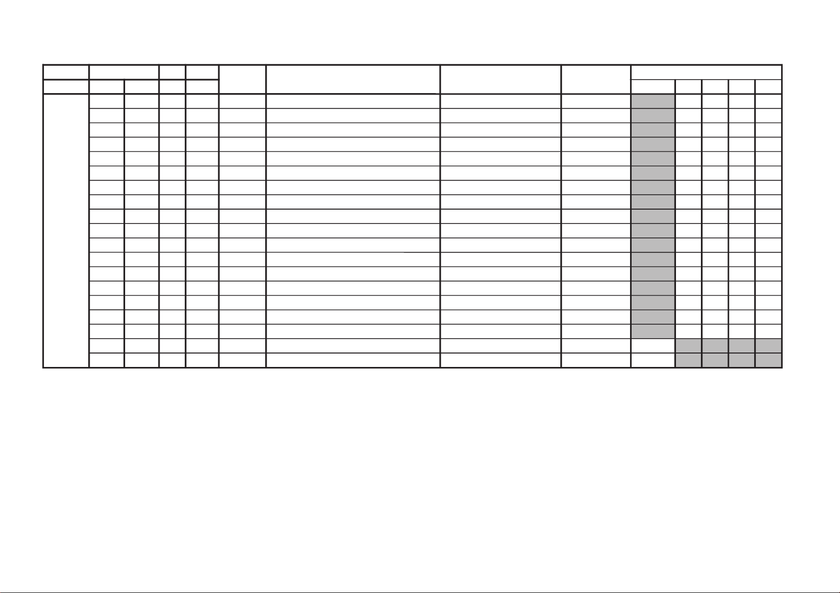
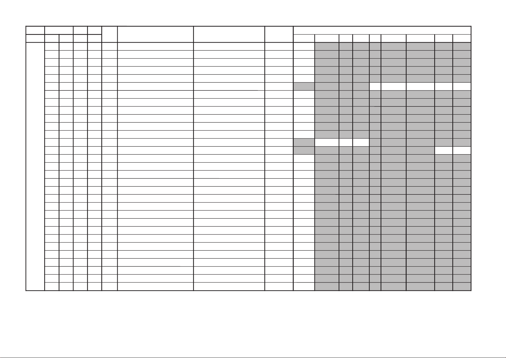
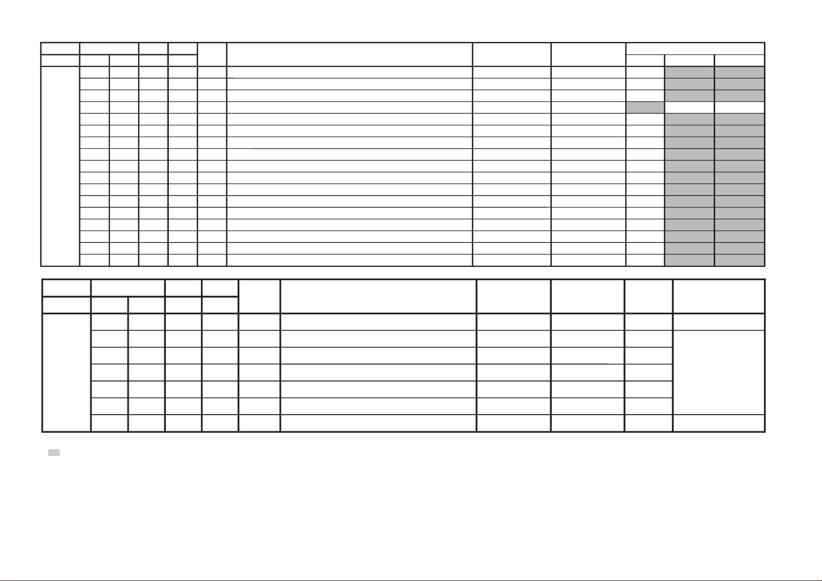
ytilanoitcnuF.tinIegnaRATADnoitcnuFetoN&elbaTemaNeciveD)deliateD(eulaVlaitinI
yrogetaC.oNemaNceDceD nommoC050605w06w
MOEG000SOPH130360TSUJDA)SH(tfihSlatnoziroH )BGRNPJ+(06w/05w/06/05rossecorP-VT
24242424
100RAPH130360TSUJDAmargolellaraPlatnoziroH06w/05w/06/05
13131313
200WOBH130360TSUJDAwoBlatnoziroH06w/05w/06/05
13131313
300NILV130360TSUJDAytiraeniLlacitreV06w/05w/06/05
13131313
400RCSV130360TSUJDAllorcSlacitreV06w/05w/06/05
13131313
500ZISH130360TSUJDA)WE(htdiWWE06w/05w/06/05
52525252
600WPWE130360TSUJDA)WP(htdiW/alobaraPWE )BGRNPJ+(06w/05w/06/05
13131313
700POCU710360TSUJDAalobaraPrenroCreppUWE06w/05w/06/05
13131313
800POCL710360TSUJDAalobaraPrenroCrewoLWE06w/05w/06/05
13131313
900ZTWE130360TSUJDAmuizeparTWE06w/05w/06/05
13131313
010PLSV130360TSUJDA)SV(epolSlacitreV06w/05w/06/05
13131313
110ZISV510360TSUJDAedutilpmAlacitreV06w/05w/06/05
51515151
210ROCS410360TSUJDA)CS(noitcerroC-S06w/05w/06/05
52525252
310SOPV130360TSUJDA)HSV(tfihSlacitreV06w/05w/06/05
13131313
410LBH000100XIFedoMgniknalBBGR06w/05w/06/05
10101010
510FBW700510XIF)FBW(gniknalBediWfognimiT06w/05w/06/05
70707070
610RBW700510XIF)RBW(gniknalBediWfognimiT06w/05w/06/05
01010101
710LBS000100XIFgniknalBecivreSenon00
810YPOC000100XIFaeraMVNzH06/05llaotatadOEGehtypoCenon00
Adjustment Item Ta ble
– 14 –
RM-W101
Page 16
– 15 –
JVTytilanoitcnuF.tinIegnaRATADnoitcnuFetoN&elbaTemaNeciveD )deliateD(eulaVlaitinI
yrogetaC.oNemaNceDceD
nommoCpmeTloC
)rehtoHGIH(
pmeTloC
)rehtoWOL(
pmeTloC
)rehtoMRON(
pmeTloC
)VUYHGIH(
pmeTloC
)VUYWOL(
pmeTloC
)VUYLAMRON(
pmeTloC
)BGRHGIH(
pmeTloC
)BGRWOL(
pmeTloC
)BGRMRON(
srehtOBGRVUYedomciP
0
edomciP
1
edomciP
2
edomciP
3
LBHW000ROKB130360TSUJDARtesffOleveLkcalB )srehtO/BGR/VU(*)lamroN/WOL/HGIH(pmetlocrossecorP-VT
131313131313131313
100GOKB130360TSUJDAGtesffOleveLkcalB )srehtO/BGR/VU(*)lamroN/WOL/HGIH(pmetloc
131313131313131313
200VRDR730360XIFRtnioPetihW )srehtO/BGR/VU(*)lamroN/WOL/HGIH(pmetlocorP-VT
737373737373737373
300VRDG730360TSUJDAGtnioPetihW )srehtO/BGR/VU(*)lamroN/WOL/HGIH(pmetloc
131313131313131313
400VRDB730360TSUJDABtnioPetihW )srehtO/BGR/VU(*)lamroN/WOL/HGIH(pmetloc
131313131313131313
500GPL000100XIFteserPniaGBGR enon10
600RGP130721XIF)RGP(RniaGteserP enon54
700GGP130721XIF)GGP(GniaGteserP enon54
800BGP130721XIF)BGP(BniaGteserP enon54
900FONG000510XIFtesffOniaGteserP enonpoolCCC51
010TRBS130360TSUJDAssenthgirB-buS VUY/BGR/srehtO
131313
110ORBS000300XIF)ciPtnegilletnI(tesffOssenthgirB-buS enon10
210LGE000100XIFmetsySCCCnipooLniaGelbanE enon00
310LGS000300XIFmetsySCCCnitnerruChgiHfonoitceleS enon00
410BKA000100XIFnoitazilibatStnerruCkcalB enon00
510SBC000100XIFgnitimiLtnerruCmaeBfoecneuqeSlortnoC enon00
610BBGR000300XIFgniknalBBGR enon00
710GBLB000100XIFtuptuOneerG&eulBfogniknalB enon00
810BFO000100XIFeulBtesffOleveLkcalB enon10
910RBSN000510XIFtesffOssenthgirBdradnatSnoN enon50
020PBW000300XIF)woL:3,2,lamroN:1,hgiH:0(gnitteSpmeTroloC edoMerutciP
00102010
120VUO000100XIFlangiStupnIVUnolortnoCtesffO VUY/srehtO
00
00
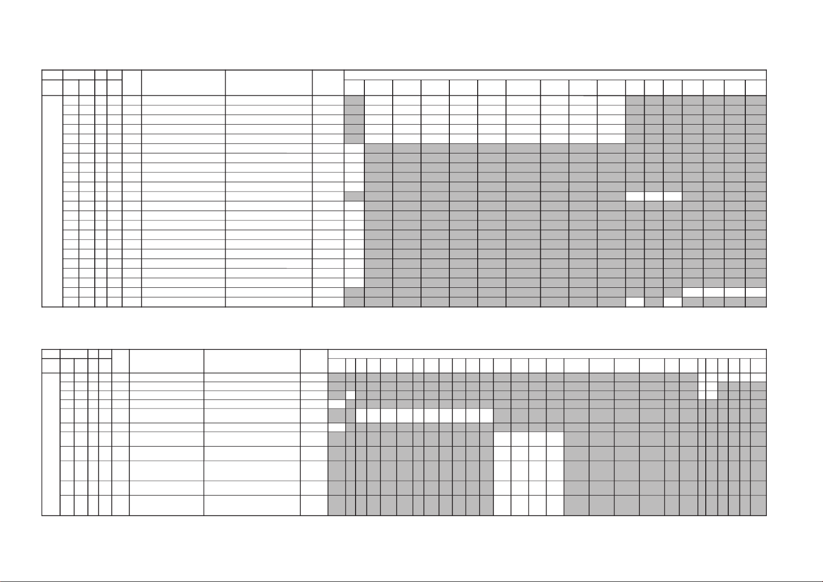
JVTytilanoitcnuF.tinIegnaRATADnoitcnuFetoN&elbaTemaNeciveD )deliateD(eulaVlaitinI
yrogetaC.oNemaNceDceD
nommoCVUYlap05
)VT(
lap05
)oediV(
maces05
)VT(
maces05
)oediV(
VT06oediV06VUY05VUY06BGR05BGR06edomciP
0
edomciP
1
edomciP
2
edomciP
3
ocE*cimanyD
)npJ(dts
ocE*cimanyD
)npJ(hcum
ocE*dradnatS
)npJ(dts
ocE*dradnatS
)npJ(hcum
dtsocE
)npJ(
hcumocE
)npJ(
VToediVVT
ediW
oediV
ediW
MVA
)npJ(
ediWVA
)npJ(
JDAS000XAMP360360TSUJDAmumixaMerutciP )BGRNPJ+(>ediW/lamroN</)ediW/lamroN(*)oediV/VT( rossecorP-VT
737373730000
100EUHS700510TSUJDAeuH-buS oediV/VT
7070
200PHSS510360XIFssenprahS-buS )BGRNPJ+(VUY/oediV/VT
53
5383
300OHSS000300XIF)ciPtnegilletnI(tesffOssenprahS-buS enon20
400LOCS130360TSUJDAroloC-buS /)oediv(maces05/)vt(maces05/)oediv(lap05/)vt(lap05
BGR06/BGR05/VUY06/VUY05/oediv06/VT06
13131313131313131313
500OOCS000300XIF)ciPtnegilletnI(tesffOroloC-buS enon20
600CIP130721XIF;)dilavni(001>,)dilav(001-0:AG[lortnoCerutciP
])dilavni(6tiberongi;)dilav(36-0:srehtO
)ataDteseRresU=lanosreP:AG(ledoMerutciP
0010856001
700LOC130721XIF;)dilavni(001>,)dilav(001-0:AG[lortnoCroloC
])dilavni(6tiberongi;)dilav(36-0:srehtO
)ataDteseRresU=lanosreP:AG(ledoMerutciP
65050405
800TRB130721XIF,)dilav(001-0:AG[lortnoCssenthgirB
tiberongi;)dilav(36-0:srehtO;)dilavni(001>
])dilavni(6
)ataDteseRresU=lanosreP:AG(ledoMerutciP
05050605
900EUH130721XIF;)dilavni(001>,)dilav(001-0:AG[lortnoCeuH
])dilavni(6tiberongi;)dilav(36-0:srehtO
)ataDteseRresU=lanosreP:AG(ledoMerutciP
05050505
010PHS130721XIF,)dilav(001-0:AG[lortnoCssenprahS
tiberongi;)dilav(36-0:srehtO;)dilavni(001>
])dilavni(6
)ataDteseRresU=lanosreP:AG(ledoMerutciP
06050505
KV-AR14M80
RM-W101
Page 17
KV-AR14M80
JVTytilanoitcnuF.tinIegnaRATADnoitcnuFetoN&elbaTemaNeciveD )deliateD(eulaVlaitinI
yrogetaC.oNemaNceDceD nommoCsrehtOBGRVUY)VT(LAP)VT(CSTN)VT(MACES)oediV(LAP)oediV(CSTN)oediV(MACESTUPNI-SMACESCSTNVT
CY000QRFP000300XIFyaleDdnaycneuqerFretneCgnikaeP rossecorP-VT00
100APR100300XIFtoohSrevO&erPoitaR rehto/VT
20
20
200OPR200300XIFskaePevitageN&evitisoPfooitaR rehto/VT
20
20
300YLDY210510XIFyaleD-Y TUPNI-S/VUY+)OEDIV/VT(*)MACES/CSTN/LAP(
9080808011901190
400TAMC000300XIFxirtaM)ASU/napaJ(CSTNroMACES-LAP )BGRNPJ(00
00
500LCA100100XIFgnitimiLroloCcitamotuA 10
600BC000100XIFycneuqerFretneCssapdnaBamorhC )xif0:oediV*(VThtiwylnodilav10
700OBS100300XIFtesffOkcalBMACES 00
800ESHC100300XIFytivitisneStnedICSTN/LAP 20
900OLC000100XIFretliF)lleB(ehcolCfoycneuqerFretneC 00
010PRTC000100XIFedoMparTamorhC srehto/MACES
00
10
110SPB000100XIFeniLyaleDdnab-esaBamorhCfossapyB srehto/CSTN
00
10
210OCF000100XIFnOroloCdecroF 00
310TNIT130360XIFlortnoCtniTdnaB-esaB srehto/VUY
13
13
410VUT000100XIFslangiSVUnolortnoCtniT 00
JVTytilanoitcnuF.tinIegnaRATADnoitcnuFetoN&elbaTemaNeciveD)deliateD(eulaVlaitinI
yrogetaC.oNemaNceDceD nommoC0506srehtoVUYVToediVtxeteleTpi-VTlangisoN
CNYS000SYS000100XIFtupnICNYSYnonoitazinorhcnyS 00
100OF000300XIFtnatsnoCemiT1esahP )FR(langisoNrogninuTotuA/txeteleT/oediV/FFOPIVT/NOPIVT
3030100000
200DIV000100XIFedoMtnedIoediV 06/05
0000
300LSF000100XIFcnySlacitreVrofleveLgnicilSdecroF 00
400LSS000100XIFrotarapeScnySleveLgnicilS 06/05
0000
500DIVS100700XIFnoitacifitnedIoediVrofnoitceleSecruoS srehtO/VUY
0070
600FROF000300XIFycneuqerFdleiFdecroF 30
700KVM000100XIFgniyeKnoisiVorcaM 10
800TCFA000300XIF,611nip:SU,AG(lortnoChctiwSgnimiTCFA
821niP:NPJ,ORUE
30
RM-W101
– 16 –
Page 18
– 17 –
JVTytilanoitcnuF.tinIegnaRATADnoitcnuFetoN&elbaTemaNeciveD)deliateD(eulaVlaitinI
yrogetaC.oNemaNceDceD nommoCVUYVToediV
WS0002VC000100XIFnoitceleSlangiStupnI2SBVC 00
100OVS100300XIF84@niPISBVC/OVS/OVFIfonoitcnuFVUY/oediV/VT
201010
200LFD000100XIFnoitcetorPhsalF 10
JVTytilanoitcnuF.tinIegnaRATADnoitcnuFetoN&elbaTemaNeciveD )deliateD(eulaVlaitinI
yrogetaC.oNemaNceDceD
nommoCsrehtOBGReviLVT
)nyD(
VT
)srehtO(
oediV
)nyD(
oediV
)srehtO(
pmeTroloC
)HGIH(
pmeTroloC
)srehtO(
roloC
)WOL(pmeT
pmeTroloC
)LAMRON(
TCIP000LDAC700510XIFleveLevirDedohtaC 00
100AFC000300XIFedoMretliFbmoC 00
200COS200300XIFleveLgnippilCtfoS 00
300LWP100100XIFhctiwSgnitimiLetihWkaeP 10
400LTHW600510XIFgnitimiLetihWkaeP 90
500MAG100100XIFammaG 00
600STW100300XIFhctertSetihWdnalortnoCammaGsrehtO/eviL
20
20
700RFT000100XIFlangiSecnanimuLfooitaRrefsnarTCD )BGRNPJ+(srehtO/eviL
100010
800ROC300300XIFgniroC )srehto/anyD(*)oediV/VT(
00000000
900OROC000100XIF)ciPtnegilletnI(tesffOgniroC 00
010SKB300300XIFhctertSkcalBsrehto/BGR
2020
110SAA100100XIFhctertSkcalBehtffohctiwSotaerAkcalB 10
210KSD000100XIFlortnoCnikScimanyD 00
310SLB000100XIFhctertSeulB )SREHTO/HGIH(pmetloc
0000
410SLBN000100XIFtiucriChctertSeulBnoitarepO 00
510RRN000100XIFnoitcudeRdeRnoN )LAMRON/WOL/HGIH(pmetloc
10
1010
KV-AR14M80
RM-W101
Page 19
KV-AR14M80
JVTytilanoitcnuF.tinIegnaRATADnoitcnuFetoN&elbaTemaNeciveDnommoC
yrogetaC.oNemaNceDceD
FIV000DFIO630360XIFrotaludomeDFItesffO rossecorP-VT63
100TCGA130360XIFrevo-ekaTCGA 13
200MTS000100XIFedoMgninuThcraeS 10
300DG000100XIFlangiS1SBVCnoyaleDpuorG 00
400SCGA100300XIFdeepSCGAFI 10
500IFF000100XIFLLPFIretliFtsaF 00
600PMAO300300XIF)metsyS'L&Lylno(edutilpmAlangiStuptuOoediV 30
700IAV000100XIF)metsyS'L&Lylno(noitcerroCedutilpmAlangiStuptuOImetsyS 00
JVTytilanoitcnuF.tinIegnaRATADnoitcnuFetoN&elbaTemaNeciveD)deliateD(eulaVlaitinI
yrogetaC.oNemaNceDceD
nommoCedomciP
0
edomciP
1
edomviP
2
edomciP
3
MV000DBGR300700XIFtuptuOMVottuptuOBGRfoyaleDenonrossecorP-VT40
100AMV300300XIFtuptuOMVfoedutilpmAenon00
200PAMV200300XIF)FFO:3,2,woL:1,hgiH:0(gnittesMVedoMerutciP
00102000
300OMMV300300XIFedoMMV 10
RM-W101
– 18 –
Page 20
– 19 –
JVTytilanoitcnuF.tinIegnaRATADnoitcnuFetoN&elbaTemaNeciveDnommoC
yrogetaC.oNemaNceDceD
MEDS000SWMF000300XIFrotaludomeDMFrofnoitceleSwodniW rossecorP-VT20
100SSQ100100XIF)ledoMAGtpecxe(edoMreifilpmA)SSQ(dnuoStilpSisauQ 00
200BPB000100XIFretliFssapdnaBdnuoSfossapyB 00
300OLMA000100XIFdnuoSMAroflangiStuptuOoiduA 00
400CVPH000100XIFlortnoCemuloVenohPdaeH 00
JVTytilanoitcnuF.tinIegnaRATADnoitcnuFetoN&elbaTemaNeciveDnommoC
yrogetaC.oNemaNceDceD
TXT000VXT930360XIFspilihProfnoitisoPlacitreVtxeteleT redoceDtxeT93
100DHT500721XIFtfihSegdEevitcAcnys-HtxeteleT 50
200RBT400510XIFssenthgirBBGRtxeteleT 11
300BCL000100XIFXETSAFrofgnitteselbane:1elbasid:0BCLtxeteleT 00
KV-AR14M80
RM-W101
Page 21
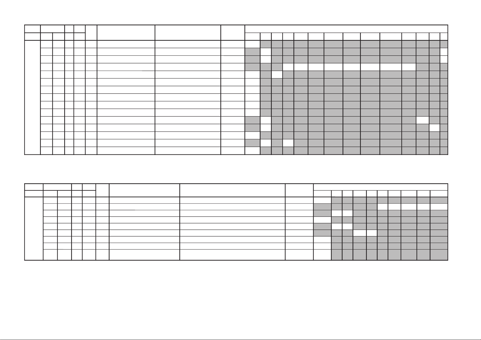
JVTytilanoitcnuF.tinIegnaRATADnoitcnuFetoN&elbaTemaNeciveD
yrogetaC.oNemaNceDceD nommoC)oruE(L-VTVToediVffOWOW/SRSdnuorrusurToeretsIonomI
PSDS000MVA200700XIFedoMLVA DSS20
100VVA500510XIFleveLecnerefeRLVA 90
200LBB000510XIFruotnoCEBB 10
300HBB000510XIFssecorPEBB 40
400WLBB000510XIFtesffOruotnoCEBB 60
500FOVS000510XIFtesffOemuloVedoMtceffE/dnuorruS onomI/oeretsI/dnuorrusurT/)WOW/SRS(ffO
5021507050
600FOVI000700XIFtesffOevitisoPemuloVretsaM 60
700FOVE000700XIFtesffOevitageNemuloVretsaM 60
800DAL000130XIFtsujdAleveLredoceD 50
900MAL000130XIFtsujdAleveLonoM 50
010NAL000130XIFtsujdAleveLmaciN 22
110SAL000130XIFtsujdAleveLPAS 80
210AAL000130XIFtsujdAleveLCDA oediV/Lnon-VT/L-VTI)oruEnoN(oediV/vT
000000
310FES300700XIFtceffEoeretS/onoMelbidercnI onomI/oeretsI
5030
410L1A000552XIFtfeLemuloV1XUA 00
510R1A000552XIFthgiRemuloV1XUA 00
610SAB800510XIFtesffOssaBniaM 00
710ERT800510XIFtesffOelberTniaM 41
8101QE800510XIFtesffO)zH001(dnaBlennahCniaMrezilauqE 70
9102QE800510XIFtesffO)zH003(dnaBlennahCniaMrezilauqE 00
0203QE800510XIFtesffO)zH0001(dnaBlennahCniaMrezilauqE 00
1204QE800510XIFtesffO)zH0003(dnaBlennahCniaMrezilauqE 01
2205QE800510XIFtesffO)zH0008(dnaBlennahCniaMrezilauqE 00
320TCFB500700XIFlortnoCEBBdnaBUD,EBD 50
420NECS100510XIFlortnoCretneCD3SRS 40
520APSS000510XIFlortnoCecapSD3SRS 10
620WHBB000510XIFedomWOWnitesffossecorpEBB 00
720ERTS200700XIFedomdnuorrusroftesffOelberT 10
820THBB000510XIFedomVTnitesffOEBB 00
920AWD000000XIF???AWD 00
030ERTT200700XIFedoMVTnitesffOelberT 20
– 20 –
KV-AR14M80
RM-W101
Page 22
JVTytilanoitcnuF.tinIegnaRATADnoitcnuFetoN&elbaTemaNeciveDnommoC
yrogetaC.oNemaNceDceD
CEDS000UTPM300510XIF)CSTB(noitcetedtolipXPMrofdlohserhTreppU DSS20
100LTPM900510XIF)CSTB(noitcetedtolipXPMrofdlohserhTrewoL 50
200UTPS300510XIFnoitcetedreirracPASrofdlohserhTreppU 80
300LTPS600510XIFnoitcetedreirracPASrofdlohserhTrewoL 51
400HT1C000130XIF1CSfonoitcetedrofdlohserhTlamroN 00
500PA1C000130XIF1CSfonoitcetedrofdlohserhTmargorPotuA 00
600HTPS000130XIFPASfoetumotuarofdlohserhTesioN 00
700YHPS400510XIFPASfoetumotuarofezissiseretsyH 30
800HTMF000130XIFdradnats2AMFni2CSfoetumotuarofdlohserhTesioN 81
900YHMF400510XIFdradnats2AMFni2CSfoetumotuarofezissiseretsyH 70
010HTTB000130XIFreirracoeretsCSTBfoetumotuarofdlohserhTesioN 00
110YHTB400510XIFoeretsCSTBfoetumotuarofezissiseretsyH 30
210HTJE000130XIFreirracbusMFJAIEfoetumotuarofdlohserhTesioN 00
310YHJE400510XIFreirracbusMFJAIEfoetumotuarofezissiseretsyH 40
410YLNO000100XIFtuptuoCEDnoMACINdetalerylnoecudorpeR 00
510MAXE000100XIF)PEDD(LdradnatsnietumotuafoesacniecruoskcabllaF 00
610TMIN000100XIF)PEDD(etarrorretibnodnepednoitcnufetumotuaMACIN 00
710ELIN001552XIF)PEDD(timilrorrerewolMACIN 05
810EUIN002552XIF)PEDD(timilrorrereppuMACIN 002
910DMPE100300XIF)PEDD(gnimmargorPysaECEDMED 20
020SDTS910130XIFsedomSSSdnaDSArofdexelpitlumstiB 13
120AMVO100100XIFnoitpadanoitaludomrevoMF 00
220WBLF000300XIFhtdiwdnabretlifrotaludomedMA/MF 30
320DMDI000300XIFedomSSSnideepstnediMF 00
420LAPF000100XIFgnidocedCSTBrofycneuqefeniL 00
520TMVO100200XIFlanimonotevitalerdlohserhtlevelnoitaludomrevO 30
620IXCD000100XIFretrevnIlortnoCgnilacSOXCDMACIN 00
720GXCD000700XIFniaGlortnoCgnilacSOXCDMACIN 00
820LLCD110510XIF)L(timiLlortnoCgnilacSOXCDMACIN 00
920HLCD000130XIF)H(timiLlortnoCgnilacSOXCDMACIN 00
030UEDI100300XIFDTS2AnaeporuErofgnittesDOMDI 00
130RKDI100300XIFDTSMnaeroKrofgnittesDOMDI 00
230PJDI100300XIFDTSJAIErofgnittesDOMDI 10
– 21 –
KV-AR14M80
RM-W101
Page 23
KV-AR14M80
JVTytilanoitcnuF.tinIegnaRATADnoitcnuFetoN&elbaTemaNeciveD)deliateD(eulaVlaitinI
yrogetaC.oNemaNceDceD nommoC0506
MTPO000THSA600700XIF)nim5*atad(remitffotuhsotuA 00
100BDSO000510XIFssenthgirbDSO h06orciM/RMM50
200HDSO500510XIFnoitisoPlatnoziroHDSO h06orciM/RMM50
300VDSO730360XIFnoitisoPlacitreVDSO 06/05h06orciM/RMM
3613
400ETUM000100XIF)delbane=1(hctiwSetuMlangiSoN 00
500LUFR510510XIF)hf0nehwelbasiD(dekcolnUretfaretnuoCegnahClangiSFR 40
600KLFR510510XIF)hf0nehwelbasiD(dekcoLretfaretnuoCegnahClangiSFR 00
700LUVA510510XIF)hF0nehwelbasiD(dekcolnUretfaretnuoCegnahClangiSVA 40
800KLVA510510XIF)hF0nehwelbasiD(dekcoLretfaretnuoCegnahClangiSVA 00
900GNAL000300XIFnoitidnocgnippihsegaugnalDSO 00
010TXTH000100XIFwsrotarepescnyS rossecorP-VT00
110SSMC000100XIFwscnyS rossecorP-VT10
210OXCD060592XIFeulaVOXCD PSD/h06orciM/RFS07
310LBXE000510XIFesioNetihWetanimilEotremiTgniknalBdednetxE 70
410SYST000300XIF )ledoMAG(]K/D:3,M:2,I:1,G/B:0[teseRtseTtaMVNnisySVTeziromeM 00
510UOVT100100XIFlangistuohtiwetuM:1,ffoetuMsyawlA:0noitidnocetumtuoVT 00
610LBL100100XIFnoitidnoClangiSoNtAnoitcudeRssenthgirB 00
JVTytilanoitcnuF
.tinIegnaRATADnoitcnuFetoN&elbaTemaNeciveDnommoCetoN
yrogetaC.oNemaN
ceDceD
BTPO
000LLAI
000100
XIF)MVNnideziromemton(hctiwSetirWdradnatS
00
1001BPO
000552
XIF)detalermetsyS(1noitpO
*****
kramerroF *****
otreferesaelP
llaroftiBnoitpO
32egaPnosledom
52egaPot
2002BPO
000552
XIF)detalerlangiSoediV(2noitpO
*****
3003BPO
000552
XIF)detalergnidoceDoeretS(3noitpO
*****
4004BPO
000552
XIF)suoenallecsiM(4noitpO
*****
5005BPO
000552
XIF)suoenallecsiM(5noitpO
*****
6006BPO
000552
XIF)detaleregaugnaLDSO(6noitpO
*****
RM-W101
– 22 –
NOTE
•
shaded items are no data.
• Standard data listed on the Adjustment Item Table are reference values, therefore it may be different for each model and for each mode.
• Note for Different Data Those are the standard data values written on the microprocessor. Therefore, the data values of the modes and stored respectively in the memory.
In case of a device replacement, adjustment by rewriting the data value is necessary for some items.
Page 24
ITEM INFORMATION
No. OPB1
KV-AR14M80
RM-W101
Item
KV-AR14M80
No. OPB2
Item
KV-AR14M80 00
Speed Search
0
SPEED SEARCH (Time of speed search) 00 = disabled (original cycle speed)
TV System Selection 0 = disabled, 1 = enabled
0
AV Multi/
PAM(GA)
1
D1(JPN)
D1 (D1 Terminal) 0 = not available, 1 = available
AV Multi/ (AV Multi Terminal) - JP 0 = not available, 1 = available
PAM Portable Audio Mode - GA 0 = not available, 1 = available
Component (Component [YCbCr] Terminals) 0 = not available, 1 = available
Composite (No. of Composite Terminals) 00 = no composite terminal
(SCART) (No. of SCART Terminals) 01 = 1 composite terminal
SECAM (SECAM Color System) 0 = not available, 1 = available
Color decoding (Color Crystal Selection) 00 = PAL/NTSC/SECAM (Multi)
M/N
01
Component
1
L’
0
Composite (SCART)
M
1
B/G
1
01 = 4 time speed from the original
10 = 6 time speed from the original
11 = 8 time speed from the original
SECAM
101
(Euro:no Scart) BX1L:No Video
(Euro:1 Scart) BX1L:2 Video in
10 = 2 composite terminals
(Euro:2 Scart) BX1L:3 Video in
11 = 3 composite terminals
(Euro:no terminal) BX1L:4 Video in
01 = NTSC (3.58MHz)
10 = PAL/NTSC/SECAM (4.43MHz)
11 = PAL/NTSC (Tri-Norma)
I
1
Color Decording
D/K
1
DEC
79
DEC
116
No. OPB3
Item
KV-AR14M80
HDEV
HDEV (High Deviation Mode) 0 = disabled, 1 = enabled
NICAM ST (NICAM Stereo) 0 = disabled, 1 = enabled
NICAM BI (NICAM Stereo) 0 = disabled, 1 = enabled
A2 ST/BI (A2 [West German]
Thai Bilingual (A2 [Thai] Bilingual)
JP/US ST (JP/US Stereo) 0 = disabled, 1 = enabled
Korean ST (Korean Stereo) 0 = disabled, 1 = enabled
MONO (Monaural Model) 0 = Stereo (SSD) Model
NICAM ST
0
NICAM BI
0
Stereo/Bilingual) 0 = disabled, 1 = enabled
or Force SAP if JP/US ST is act 0 = disabled, 1 = enabled
0
A2 ST
0
Thai
Bilingual
JP/US ST
0
1 = Monuaral Model
0
Korean ST
0
MONO
0
DEC
00
– 23 –
Page 25

KV-AR14M80
RM-W101
No. OPB4
Item
KV-AR14M80
No. OPB5
Item
KV-AR14M80
V-Chip
0
1 = 1 speaker Models
1 = Off/Simulated/WOW/TruSurround (US)
1 = Off/Simulated/SRS (3D) Surround (GA)
1 = Parental Control Model (rating)
IP Plus
1
1 = Full Surround Model
(Off/simulated/surround/
SRS/WOW/TruSurround)
1
0
Surround
0
Tilt
0
Firmware/
SMAT
1
Firmware (SSD Firmware Downloading) 0 = disabled, 1 = enabled
SMAT Surround Matrix 0 = Active, 1 = Passive
1 spk Models 1 Speaker Models 0 = 2 or 3 Speaker Models,
VM (Velocity Modulation) 0 = disabled, 1 = enabled
Equalizer (5-band Equalizer Model) 0 = Bass/Treble Model, 1 = Equalizer Model
Surround (US/GA Surround Selection) 0 = Off/Simulated/Surround
V-Chip (V-Chip Model) 0 = Channel Block Model (no rating)
TOP (Forced TOP) 0 = Auto Mode (TOP/FLOF), 1 = Forced TOP
TEXT (Teletext Model) 0 = Non-Teletext Model, 1 = Teletext Model
Full
Surround
0
Full Surround (Full Surround option) 0 = Normal Surround Model
No Surround (No Surround Model) 0 = Surround Model, 1 = Non-Surround Model
Forced 60 (Forced 60Hz in no signal) 0 = 50Hz, 1 = 60Hz
ASD (Automatic Standard Detection) 0 = disabled, 1 = enabled
Tilt (Tilt Correction/PIC Rotation) 0 = disabled, 1 = enabled
IP Plus (Intelligent Picture Plus) 0 = disabled, 1 = enabled
IP (Intelligent Picture) 0 = disabled, 1 = enabled
Wide (Wide Mode/V-Compressed) 0 = disabled, 1 = enabled
1 spk
Models
0
No
Surround
0
VM
Forced 60
Equalizer
0
ASD
0
To p
0
IP
1
Tex t
0
Wide
1
DEC
144
DEC
07
– 24 –
Page 26

No. OPB6
KV-AR14M80
RM-W101
Item
KV-AR14M80
0
Feature 1
0
OSD Language Selection
0010
1 = Taiwan/Korea/Philippine
(Wake-up timer enable)
(GA Surround Spec:OFF,
SIMULATED, SRS)
1 = Latin (Volume Figure Display)
1 = Comb available
1 = PiP available
0xx1 = Portuguese
US 1x1x = Complicated Chinese
(GA NTSC) 1xx1 = Korean
1xxx = Simplified Chinese
GA x1xx = Arabic
xx1x = Thai
xxx1 = Vietnamese
DEC
132
GA US
1
GA US (US Model Destination) 0 = US/CANADA/Latin
Latin (US Model Latin Destination) 0 = US/CANADA (No Volume Figure Display)
Feature 2 (Temporary for BX1L) 0 = Comb Not available
Feature 1 (Temporary for BX1L) 0 = PiP Not Available
OSD Language Selection 01xx = French
(English always available except JP) US 0x1x = Spanish
Latin
Feature 2
0
0000 = Destination ADE
EU 0001 = Destination BL
0010 = Destination KR
0011 = Destination U
– 25 –
Page 27

KV-AR14M80
RM-W101
3-3. PICTURE QUALITY ADJUSTMENTS
PMX/CONTRAST ADJUSTMENT
1. Select Video Mode.
2. Input PAL CB to TV set.
3. Set PICT 03 "PWL" to 00h and WHBL 21 "BLBG" to 01h.
4. Set the following condition:
PICTURE 100%, COLOR 0%, BRIGHTNESS 50%.
5. Connect an oscilloscope to pin 4 (R output) of CN004.
6. Set to Service Mode "PWL" to 00h, "BLBG" to 01h.
7. Select SADJ00 "PMX" with
commander then adjust VR within spec with
1.46 ± 0.03 Vp-p = without VM models
1.65 ± 0.03 Vp-p = with VM models
8. Then press [MUTING] t
9. Set "PWL" and "BLBG" back to initial data repectively.
(PWL: 01h and BLGG: 00h)
1 and 4 of the
3 and 6.
VR
Black
- to write the data
SUB HUE ADJUSTMENT
1. Select Video.
2. Input a NTSC 3.58 Color Bar to TV set.
3. Set the following condition:
PICTURE 100%, COLOR 50%, BRIGHTNESS 50%
4. Connect an oscilloscope to pin 2 (B output) of CN004.
5. Set to Service and adjust SADJ01 "SHUE" with
1
and 4 of commander then adjust to VB1 = VB2 =
VB3 = VB4 with
6. Then press [MUTING] t
3 and 6.
VB1
VB2
- to write the data.
VB3
VB4
The highest level of VB1, VB2, VB3, VB4 must be
aligned at the same time.
The ideal difference between VB2 and VB3 is within
±110mV.
For single system with NTSC 4.43 select TV channel
with NTSC 4.43 and repeat 4 t 6.
SUB COLOR ADJUSTMENT
1. Select Video and set Picture mode.
2. Input PAL 100% CB to TV set.
3. Set PICT 06 "WTS" to 00h.
4. Set the following condition:
PICTURE 100%, COLOR 50%, BRIGHTNESS 50%.
5. Connect an oscilloscope to pin 2 (B output) of CN004.
6. Select to Service Mode and adjust SADJ04 "SCOL"
with
1 and 4 of commander then adjust to
VB2 = VB3 = VB4 with
VB1
VB2 = VB3 = VB4
(Difference is within 70mV)
7. Then press [MUTING] t
3 and 6.
VB2 VB3 VB4
- to write the data.
8. Set "WTS" back to original data.
3-4. DEFLECTION ADJUSTMENT
H-TRAPEZOID ADJUSTMENT
1. Receive cross hatch/dotsignal.
2. Adjust on to make H-Trapezoid distortion best.
NORMAL MODE (50Hz)
1. Set to Service Mode.
2. Input SPCB Signal (Select Video Mode for USA).
3. Using the
Mode).
4. Rasie/lower data using the
the following items:-
GEOM : 000 HPOS Horizontal Shift (HS)
1 and 4 button select GEO (Service
3 and 6 buttons adjust
001 HPAR Horizontal Parallelogram
002 HBOW Horizontal Bow
003 VLIN Vertical Linearity
004 VSCR Vertical Scroll
005 HSIZ EW Width (EW)
006 EWPW EW Parabola/Width (PW)
007 UCOP EW Upper Corner Parabola
008 LCOP EW Lower Corner Parabola
009 EWTZ EW Trapezium
010 VSLP Vertical Slope (VS)
011 VSIZ Vertical Amplitude
012 SCOR S-Correction (SC)
013 VPOS Vertical Shift (VSH)
014 HBL RGB Blanking Mode
015 WBF Timing of Wide Blanking (WBF)
016 WBR Timing of Wide Blanking (WBR)
017 SBL Service Blanking
018 COPY Copy the GEO data to all
50/60Hz NVM area
5. Write into memory by pressing [MUTING] then - on
the remote commander.
– 26 –
Page 28

KV-AR14M80
RM-W101
WIDE MODE (50Hz)
(V-Compression Adjustment)
1. Input SPCB signal.
2. Adjust condition change to WIDE MODE : ON
3. Copy (Item from normal mode 50Hz) all Normal
Mode adjusted data.
NORMAL MODE (60Hz)
1. Input 525/60Hz signal.
2. They can copy 50Hz first.
("COPY" under GEOM is set to
3. Using the
(Service Mode).
4. Raise/lower data using the
obtain optimum image.
GEOM : 000 HPOS Horizontal Shift (HS)
1 and 4 button, select category GEO
001 HPAR Horizontal Parallelogram
002 HBOW Horizontal Bow
003 VLIN Vertical Linearity
004 VSCR Vertical Scroll
005 HSIZ EW Width (EW)
006 EWPW EW Parabola/Width (PW)
007 UCOP EW Upper Corner Parabola
008 LCOP EW Lower Corner Parabola
009 EWTZ EW Trapezium
010 VSLP Vertical Slope (VS)
011 VSIZ Vertical Amplitude
012 SCOR S-Correction (SC)
013 VPOS Vertical Shift (VSH)
014 HBL RGB Blanking Mode
015 WBF Timing of Wide Blanking (WBF)
016 WBR Timing of Wide Blanking (WBR)
017 SBL Service Blanking
018 COPY Copy the GEO data to all
50/60Hz NVM area
1, then [MUTE] + -)
3 and 6 buttons to
WIDE MODE (60Hz)
(V-Compression Adjustment)
1. Input mono scope signal.
2. Adjust condition change to WIDE MODE : ON
3. "COPY" is set to
1, then [MUTE] + -
3-5. DRIVE ADJUSTMENT
1. Input signal 70% Color Bar (USA)
100% Color Bar (Other)
2. Make sure only red is active.
3. Set following condition :-
PICTURE 100%, COLOR 0%, Other 50%
4. Select SADJ00 "PMAX" with
until voltage in R out X gain
5. Then press [MUTING] t
X±2VDC (R Cathode on C or CV board)
1 and 4 then adjust
[recorded] = SPEC
- to write data.
Model 14” 21”
GA 83.0 88.0 - Non VM Models
99.0 - VM Models
6. Set VIDP 36 BLBG back to 00.
– 27 –
Page 29

KV-AR14M80
RM-W101
3-6. PICTURE DISTORTION ADJUSTMENT
H. CENTER ADJUSTMENT (HPOS)
1. Input NTSC Monoscope signal.
2. Activate the Service Adjustment Mode.
3. Select the HPOS item with
4. Adjust the value of HPOS with
vertical center.
5. Press [MUTING] then
H. SIZE ADJUSTMENT (HSIZ)
1. Input NTSC Monoscope signal.
2. Activate the Service Adjustment Mode.
3. Select HSIZ with
4. Adjust with
1 and 4.
3 and 6 for the best horizontal size.
5. Press [MUTING] then
1 and 4.
3 and 6 for the best
- to save into the memory.
- to save into the memory.
V. LINEARITY (VLIN), V. CORRECTION (SCOR), PIN
AMP (EWPW), AND HORIZONTAL TRAPEZOID
(EWTZ) ADJUSTMENTS
1. Input NTSC Monoscope signal.
2. Activate the Service Adjustment Mode.
3. Select VLIN, SCOR, EWPW, and EWTZ with
4.
4. Adjust with
5. Press [MUTING] then
V LINEARITY (VLIN)
V CORRECTION (SCOR)
PIN AMP (EWPW)
3 and 6 for the best horizontal size.
- to save into the memory.
1 and
V. SIZE ADJUSTMENT (VSIZ)
1. Input NTSC Monoscope signal.
2. Activate the Service Adjustment Mode.
3. Select the VSIZ item with
4. Adjust value of VPOS with
1 and 4.
3 and 6 for the best
vertical center.
5. Press [MUTING] then
- to save into the memory.
V. CENTER ADJUSTMENT (VPOS)
1. Input NTSC Monoscope signal.
2. Activate the Service Adjustment Mode.
3. Select the VPOS item with
4. Adjust value of VPOS with
1 and 4.
3 and 6 for the best
vertical center.
5. Press [MUTING] then
- to save into the memory.
HORIZONTAL TRAPEZOID (EWTZ)
V. ANGLE (HPAR), H. BOW (HBOW), UPPER PIN
(UCOP) AND LOW PIN (LCOP) ADJUSTMENTS
1. Input NTSC Monoscope signal.
2. Activate the Service Adjustment Mode.
3. Select HPAR, HBOW, UCOP, and LCOP with
4.
4. Adjust with
5. Press [MUTING] then
V ANGLE (HPAR)
V BOW (HBOW)
3 and 6 for the best picture.
- to save into the memory.
1 and
– 28 –
UPPER PIN (UCOP)
LOW PIN (LCOP)
Page 30

4-1. BLOCK DIAGRAM
Stdby Power
STBY 3.3/5V
Relay
JP
CXA2085
Detect
Video
JP
EU
VIF SAW
SIF SAW
MAIN
Power
Supply
FSS TUNER
AGCin
12C
TV
L(Mono)
R
Video
L(Mono)
R
CV/YC
L(Mono)
R
CV
L(Mono)
R
CV/YC
L(Mono)
R
S1
S2
G/Y
B/P
B
R/P
R
L
R
Fbl(RGBin)
24.576MHz
DVD/RGB
AV2
AV3
AV1
Op Amp
Op Amp
TV
out
Mon
out
AV1
in
AV2
in
AV3
in
RGB/
DVD
in
YP
BPR
5V 30V
IF
24-5.VIF1~229-30.SIF1~12
115.P3.0
STBY
3.3V
AC in ~
110-220V
CISPR/
PFC
1.8
V
5V 8V
3.3/5V
Relay
8V AUDIO VCC
HV
DGC
+/-15V
Hout
FBT
L
2ch
Audio Amp
AT T
VAR
NVM
Pin out
H-drive
H-out
Rot. cct
V-out
VM
RGB Amp
feedback
10W
R
10W
L,R
HP
mute
EHT, ABL
LR
Hp
Ik
EW, Hd
V+, V-
RGB
+B
On/Off
Stdby
Device 12C
12C
SIRCS
Mode 1,2
Key buttons
PLL
I/O Port
A
D
C
I/O Port
VIF & SIF POWER
Color
Decoder
YUV
Processor
Jungle
RGB
Stereo
DSP
DAC
ONE CHIP IC
Micro
Te xt
CC & V-chip
11.Xtalout
10.Xtalin
74~76.YUVout
70-72.RGB2 in
34,35.InL,R5
78-80.RGB3
119.ADC2
126.INT2
116.ADC1,103P03
98, 99. SDA1, SCL1
108, 109. SDA0, SCL0
102.P0.4
122~3.P2.4~5
77.Fbl3
52.C4
49,50.InL,R4
51.CV/Y4
120.P3.3(S2)
62,63.HPL,R
48.SVO
44.Intco
33.SNDIF
31.AGCout
43.IFVO
85~87
RGBout
84.lk
65.SVM
23. V+
22. V-
112.PWMO
113.P2.2
21.EWD
67.Hout
66.Fbiso
32.EHTO/OVP
83.BCKin
LSL,R
60,61.
106.P0.2
105.P0.1
36,37.OutL,R1
111.P2.0(ST)
58.CV/Y3
59.C3
56,57.InL,R3
55.CV/Y2
53,54.InL,R2
B-INT
LED
+B line
30V
114.P2.3
D1
ID1
I
R
Radio
BPF
– 29 –
DIAGRAMS
SECTION 4
RM-W101
KV-AR14M80
Page 31

KV-AR14M80
RM-W101
4-2. CIRCUIT BOARDS LOCATION
A Board
4-3. SCHEMATIC DIAGRAM INFORMATION
Note:
• All capacitors are in µF unless otherwise noted.
• All electrolytic capacitors are rated at 50V unless otherwise
noted.
• All resistors are in ohms.
kΩ = 1000Ω, MΩ = 1000kΩ
• Indication of resistance which does not have rating
electrical power is as follows.
Pitch: 5 mm
Rating electrical power 1/4W (CHIP: 1/10W)
• : nonflammable resistor.
• : fusible resistor
• : panel designation or adjustment for repair.
• All variable and adjustable resistors have characteristic
curve B unless otherwise noted.
• Readings are taken with a color-bar signal input.
no mark : Common
( ) : PAL
[ ] : NTSC 3.58
• Readings are taken with a 10 MΩ digital multimeter.
• Voltage are dc with respect to ground unless otherwise
noted.
• Voltage variations may be noted due to normal
production tolerances.
• All voltage are in Volt.
• ✽ : Cannot be measured.
• Circled numbers are waveform references.
• : B +bus.
• : B –bus.
• k : signal path.
Note: The reference number which starts with Wxxx
(eg: W003) indicates a wire to wire connection.
Note: Components marked as XX are not fitted on this
model.
C Board
Reference information
RESISTOR : RN METAL FILM
: RC SOLID
: FPRD NONFLAMMABLE CARBON
: FUSE NONFLAMMABLE FUSIBLE
: RS NONFLAMMABLE METAL
OXIDE
: RB NONFLAMMABLE CEMENT
: RW NONFLAMMABLE
WIREWOUND
: ✽ ADJUSTMENT RESISTOR
COIL : LF-8L MICRO INDUCTOR
CAPACITOR : TA TANTALUM
: PS STYROL
: PP POLYPROPYLENE
: PT MYLAR
: MPS METALIZED POLYESTER
: MPP METALIZED POLYPROPYLENE
: ALB BIPOLAR
: ALT HIGH TEMPERATURE
: ALR HIGH RIPPLE
Note: The component identified by shading and
mark ! are critical for safety. Replace only
with part number specified.
Note: “A” board schematic diagram is divided into 6 blocks.
Each block is named by its function and block
“alphabet”. eg: Processor (Block A)
Joint connection between boards can be identified
using the block alphabet followed by sequence
numbering.
eg: -<HOUT-DEFL (A10) To D11
Meaning: Block A joint A10 is connected to Block D
joint D11
– 30 –
Page 32

J
2kV
4700p
E
C752
1000p
B
C782
1
1P
CN705
GND
1SS119-25
1SS119-25
D780
D781
L750
XX
22uH
L780
Q701
XX
CHIP
XX
R775
CHIP
XX
R777
R766
XX
R767
XX
R768
XX
R784
XX
R785
XX
R786
XX
UDZSTE-175.6B
D782
CHIP
XX
R776
CHIP
:CHIP
XX
R778
250V
4.7
C754
JW702
XX
C759
XX
CH
1
2
3
4
5
WHT
5P
CN703
200V
NC
GND
H1
NC
3
4
5
6
7
8
9
10
11
13
1
GND
GND
1
J751
110M
RV750
XX
R760
1/2W
100
R763
1/2W
100
R764
1/2W
100
R765
1/2W
560k
R773
1/2W
1k
R756
1/2W
1k
R757
1/2W
1k
R758
HSS82-TJ
D756
HSS82-TJ
D755
HSS82-TJ
D754
R774
150
3W
RS
1/2W
100
R783
R713
0
C783
1000p
B:CHIP
1
CN704
1P
1000V
13 987654
2
TDA6108AJF/N1
IC751
B IN
G IN
R IN
GND
IK
VDD
R OUT
G OUT
B OUT
0.47
R794
GP08D
D750
1/2W
470k
R780
1/2W
FPRD
100K
R795
1
2
3
4
5
6
7
7P
CN701
WHT
GND
B
G
R
GND
1K
9V
1000p
B:CHIP
C786
XX
C753
500V
1000p
C787
RS
R781
0.47
JW1781
5MM
JW1782
5MM
5MM
JW1783
:CHIP
680
R752
CHIP
680
R753
:CHIP
680
R754
250V
10
C751
250V
4.7
C781
XX
C788
XX
C790
XX
C789
XX
L781
XX
L782
XX
L783
R-IN
C
FV
RCV
(VIDEO AMP)
B-BX1S12314-E..-C..-AR14M80
1
2
3
4
5
6
9V
9V
1000V
200V
H
KG G2
CV
KR G1
G4
HV
KB
A34LRG70X
PICTURE
TUBE
TO EARTH
COATING ASSY
TO A BOARD
(DEFLECTION)
CN801
TO A BOARD
(PROCESSOR)
CN004
2W
I
H
G
F
E
D
C
B
A
4-3-1. C Board Schematic Diagram
12345 6 7
– 31 –
KV-AR14M80
RM-W101
Page 33

4-3-2. A Board — Processor (Block A)
123456789101112
A
A
GND
KEY
NC
PROCESSOR
BLOCK A
1
2
3
JR1010
XX
CHIP
B_INT
B_DAT
R097
220
CHIP
5V
R099
CHIP
220
R096
CHIP
220
Q007
UN2216
R LED SW
SPB-25MVWF
R087
220
CHIP
D914
LED
G
R
B
C
D
E
F
G
H
I
J
3P:S-MICRO
TO TOP CONTROL
PANEL
To F27 (A64) B_CLK
To F29 (A63) B_INT
To F28 (A62) B_DAT
AUDIO-STDBY
To B7 (A61)
CN005
WHT
R098
220
CHIP
Q006
UN2216
G LED SW
C333
470
10V
R398
10
CHIP
KV-AR14M80
RM-W101
KV-AR14M80
RM-W101
13 14
CN007
XX
WHT
TO A BOARD
(JACK)
CN004
XX
PWR-OFF-MUTE
(A1) To B6
3.3V
5V
C003
100p
CHIP
R004
100
3.3V
CHIP
C001
100p
CHIP
R002
R006
100
XX
CHIP
CHIP
C318
0.1
16V
B:CHIP
R393
C002
100
470
CHIP
16V
R014
3.3V
3.3V
4
3
2
1
IC003
M24C16-WMN6T(A)
NVM
3.3V
R324
100
0
CHIP
CHIP
R338
2.2k
R340
CHIP
10k
C020
CHIP
0.1
16V
B:CHIP
C308
0.01
B:CHIP
D055
UDZSTE-175.6B
25V
C015
XX
D067
XX
R331
100
CHIP
C008
47
35V
PROTECTION
UDZSTE-175.6B
R003
4.7k
CHIP
D068
R380
100
CHIP
MSD601-RT1
C314
470
10V
F
R361
CHIP
R023
1.5K
CHIP
XX
R015
1.5k
CHIP
Q013
R360
CHIP
3.3V
0
R001
4.7k
CHIP
R392
CHIP
10K
3.3V
D056
MMDL914T1
PROTECTION
IC002
RPM7240-H5
IC RECEIVER
VCC
R362
XX
CHIP
R322
4.7k
CHIP
D066
GP08D
OUT
GND
C009
R363
XX
0
B
CHIP
D054
UDZSTE-175.6B
PROTECTION
R336
4.7k
CHIP
R030
100
CHIP
C091
100p
CHIP
R320
4.7k
CHIP
D071
MMDL914T1
D072
MMDL914T1
9V (A2) To B4,B14,C8,
D14,E13,F6
C006
100
16V
L003
10uH
C004
100
16V
3.3V
C010
470p
CHIP
1.8V MAIN
R029
100
CHIP
C011
L009
10uH
XX
C311
2.2
R319
XX
CHIP
1.8V MAIN
SDA-0 (A5) To E14
3.3V (A3) To C1,D18
5V (A4) To C9,D12,E16,F1
5V
D003
D002
MMDL914T1
MMDL914T1
12
R010
10k
CHIP
C090
100p
D070
CH
XX
L012
10uH
L013
10uH
SCL-0 (A6) To E15
MOMUTE-AUDIO
(A7) To B8
C005
100
16V
R394
4.7k
CHIP
Q016
UN2211
C312
1000p
B:CHIP
C012
0.22
16V
C313
B:CHIP
1000p
B:CHIP
R337
R339
R341
R018
D069
D076
XX
C014
0.22
16V
B:CHIP
C018
0.22
16V
B:CHIP
1.8V AUDIO
D1_JP/MODE2_
EU/MONSW-MONO
(A8) To F24
1.8V AUDIO
C328
TP03
0.01
25V
CHIP
R323
CHIP
R020
100
L011
10uH
C021
100p
2.2k
R012
470
CHIP
100
CHIP
100
CHIP
CHIP
100
ROT_CTRL
To D16 (A33)
ROT_SW
To D17 (A34)
MMDL914T1
100
R024
CHIP
JR1011
0
CHIP
C013
100 16V
R026
100
CHIP
R025
100
CHIP
C325
0.022
25V
CHIP
100
CHIP
CHIP
CHIP
1.8V MAIN
UN2211
RGB-MUTE
3.3V
C023
2.2
16V
B:CHIP
97
98
99
100
101
102
103
104
105
106
107
108
109
110
111
112
113
114
115
116
117
118
119
120
121
122
123
124
125
126
127
128
TP02
C022
0.22
16V
B:CHIP
L032
10uH
WHT
TO C BOARD
CN701
D057
Q001
MMDL914T1
R-MUTE
(SPOT)
D024
L006
10uH
16V
VDDA2
VSSADC
VDDADC(1.8)
VSSP2
VSSC4
VDDC4(1.8V)
10uH
L010
MMDL914T1
UDZSTE-179.1B
PROTECTION
10uH
C026
47
35V
C028
0.1
B:CHIP
16V
9192939495
90
GNDA
VREFAD
VDDA(1.8)
VREFAD_PO
VDDA3(3.3V)
VREF_POS_LSL
VREF_NEG_LSL+LSR
VREF_POS_LSR+HPL
470
10V
C029
L036
10uH
L033
10uH
W060
0.01
R397
1.5M
CHIP
3.3V
W011
L035
XX
C031
UDZSTE-179.1B
PROTECTION
D025
UDZSTE-179.1B
PROTECTION
C025
0.22
B:CHIP
L031
10uH
96
SIRSC
SCL1
SDA1
VDDC2
VSSC2
B INT
D1_JP/MODE2_EU/MONSW-MONO
MOMUTE-AUDIO
AUDIO STDBY
AUDIO MUTE
HD SW
SCL0
SDA0
VDDP(3.3V)
S1/VC(GA)
ROT CTRL
ROT SW
STBY_SW
DGC RELAY
D1_JP/MODE1_EU
VDDC1(1.8V)
DECV1V8
KEY
S2
VSSC1/P
RED LED
GREEN LED
VDDC3(1.8V)
VSSC3
AGC-MUTE
SECAM L-L
M-SYS-IF
C024
22
MMDL914T1
GND
B OUT
G OUT
R OUT
1
23456
R
G
B
D058
MMDL914T1
G-MUTE
D059
B-MUTE
D023
C036
C030
100
0.22
16V
CHIP
CHIP
B
CHIP
100
100
R038
100
R039
R041
CHIP
8586
878889
R OUT
B OUT
G OUT
10
11
VDDA(3.3V)
VREFAD_NE
(
1
vREF_NEG_HPL+HPR
VREF_POS_HPR
XTALIN
XTALOUT
VSSA1
X001
XX
XX
R011
C032
1K
C034
CHIP
XX
L037
W022
C321
25V
B:CHIP
C322
0.001
B :CHIP
R310
R309
CHIP
1M
CHIP
D061
CN905
Y OUT
GNDIK9V
7
1
234
Y OUT
V OUT
5V
C097
XX
16V
F
10uH
4.7
UDZS-TE17-9.1B
R364
1k
L007
PROTECTION
C037
D075
CHIP
16V
XX
D004
C038
PROTECTION
0.1
PROTECTION
C302
16V
R386
CHIP
C301
2.2
B
100
16V
CHIP
470p
CHIP
F
CH
2.2k
R385
C092
R384
100
100
CHIP
CHIP
81828384
IK
VP3
ABL
GND3
B-Y/BIN
9
IC001
DECDIG
VP1
PH2LF
PH1LF
100
16V
C304
12k
R044
C300
0.22
16V
B:CHIP
C044
2.2
C041
16V
4700
F:CHIP
B:CHIP
C317
220
C042
0.22
16V
L008
10uH
B:CHIP
R316
XX
CHIP
3.3V
W008
R311
47k
CHIP
C079
XX
R326
XX
RN-CP
C084
ABL
XX
R327
B
UDZSTE-175.6B
RN-CP
7980
CHIP
B
16V
XX
FB001
1.1uH
Y/GIN
GND1
C048
C046
6800
25V
CHIP
25V
0.22
C049
0.022
CHIP
5V
R314
6.8k
CHIP
R-Y/RIN
SECPLL
B
7778
16V
ABL-BUFFER
W009
R042
TDA12067H/N1B0B0QX
SYSTEM CONTROLLER
- VIDEO PROCESSOR
- AUDIO PROCESSOR
VGUARD
13 14 15 16 17 18 19 20 21 22 23 24 25 26 27 28 29 30 31 32
24.576MHz
100
D060
GND
U OUT / FB
GND
V OUT
5
U OUT
C099
XX
16V
F
C098
XX
16V
F
D007
XX
PROTECTION
D006
XX
R356
CHIP
0
D005
XX
C053
0.022
25V
CHIP
C093
0.1
0.1
16V
16V
CHIP
B
CHIP
76
YOUT
UOUT
VOUT
SCARTFBL
)
3
2
DECBG
EWD
VD-
VD+
C052
CHIP
1000
B
B
CHIP
R048
100
CHIP
CHIP
R046
R045
100
100
CHIP
C050
10
B
C081
1000
B:CHIP
C080
1000
B:CHIP
D062
SLICER
UDZSTE-175.6B
Q009
XX
CN009
Y IN / G
1
U IN
Y IN
U IN
Y IN
C068
XX
16V
F
PROTECTION
D008
XX
PROTECTION
C095
C094
0.1
0.1
16V
B
16V
B
CHIP
CHIP
B
16V
737475
UIN
YIN
YSYNC
4
VIFIN1
VIFIN2
VSC
C089
1000
B
CHIP
C055
0.15
250V
PP
D065
PROTECTION
UDZSTE-175.6B
D064
UDZSTE-175.6B
PROTECTION
R315
6.8k
CHIP
XX
5P
YEL
GND
U IN / B
V IN / R
3
4
2
V IN
C071
XX
16V
F
C051
XX
16V
F
D009
XX
C056
C054
0.1
16V
B
R056
100
CHIP
C096
0.1
CHIP
B
69707172
68
VIN
VSSCOMB
VDDCOMB
IFVO/IF_MON_OUT
SIFAGC/SCART
IREF
GNDIF
SIFIN1
R051
39k
CHIP
C323
0.001
B:CHIP
MMDL914T1
1.8V AUDIO
+B (A9) To C11,D15,E11
GND
+BNCGND
5
1
2
V IN
9V
100
16V
L005
10uH
R058
100
R059
CHIP
1k
CHIP
6
8
7
656667
VM
AFC
HOUT
CVBS0
SCARTHPR
SCARTHPL
LSR
LSL
C1
CVBS1/Y1
INR1
INL1
CVBS3
INR3
INL3
C2
CVBS2/Y2
INR2
INL2
MON-OUT
VP2
AGC2SIF
VCC8V
INTC0-IF
PLLIF
GND2
MONO_OUTL
DECSDEM
OUTR
OUTL
D1 RIN
D1 LIN
AVL/2SIF
SIFIN2
AGCOUT
EHT0
R312
1M
R060
CHIP
100
CHIP
C058
1000
B:CHIP
D063
OCP
CN003
XX
4P
WHT
64
63
62
61
60
59
58
57
56
55
54
53
52
51
50
49
48
47
46
45
44
43
42
41
40
39
38
37
36
35
34
33
3
R317
3.3k
CHIP
R395
100k
CHIP
B:CHIP
C063
0.1
16V
TO C BOARD
VM OUT
4
MSB709-RT1
W010
C065
R313
150k
CHIP
3.3V
TP04
3.3
R377
CHIP
Q010
5
CN711
1.5k
5V
MMDL914T1
HOUT-DEFL (A10) To D11
AFC-DEFL (A11) To D2
W003
C072
0.01
25V
B:CHIP
C303
100
16V
C316
0.47
10V
B:CHIP
C309
W030
W031
C064
R379
2.2
68k
CHIP
D074
1.8V AUDIO
LSL-AUDIO (A13) To B2
LSR-AUDIO (A12) To B3
5V
W004
5V
L004
47uH
C319
47p
CHIP
C069
0.1
16V
B:CHIP
TV-L
W032
2.2
XX
C073
5V
B-BX1S12314-E..-A..(Block D)-AR14M80
SCARTFBL/A16 (A14) To F16
CVBSO (A15) To F23
SCARTHPR (A16) To F22
SCARTHPL (A17) To B1,F21
C1 (A18) To F8
CVBS1/Y1 (A19) To F10
INR1 (A20) To F12
INL1 (A21) To F11
CVBS3 (A22) To F13
INR3 (A23) To F15
INL3 (A24) To F14
CVBS2/Y2 (A25) To F20
INR2 (A26) To F18
INL2 (A27) To F19
W034
47p
MON-OUT (A28) To F5
IFVO/IF_MON_OUT (A29) To E5
PLL1F (A65) To E18
W033
C320
CHIP
JW1088
XX
5
5
5
5
5
JW1092
XX
JW1089
XX
JW1090
XX
JW1091
XX
MONO_OUTL (A30) To E19,F2
OUTR (A31) To F4
TV-R
OUTL (A32) To F3
To F17 (A54) S2
To F9 (A53) S1/VC
To F25 (A52)
D1_JP/MODE1_EU
To E21 (A68) VDDC3_CAP
1.8V_AUDIO
To B13,C10 (A50)
To E12 ( A51) AGC-MUTE
To C2 (A49) 1.8V_MAIN
To D19 (A66) PH2LF
To E20 (A67) VDDC4_CAP
To D4 (A47) ABL
To D3 (A46) VGUARD-DEFL
To E7 (A41) VIFIN2-IF
To E8 (A42) VIFIN1-IF
To D7 (A44) VD--DEFL
To D5 (A43) VD+-DEFL
To D1 (A45) EWD-DEFL
To E3 (A35) 2SIF
To E1 (A39) SIFIN2-IF
To E2 (A40) SIFIN1-IF
To D8 (A38) OVP-DEFL
To E10 (A36) TUAGC-IF
To D10 (A37) OCP-PROTECT
To B9 (A60) AUDIO-MUTE
(A59) RESET
To E9 (A55) M-SYS-IF
To C13 (A58) STBY_SW
To E6 (A56) SECAM-L-L
To C15 (A57) DGC-RELAY
– 32 – – 33 –
Page 34

4-3-3. A Board — Audio (Block B)
123456789101112
A
KV-AR14M80
RM-W101
KV-AR14M80
RM-W101
13 14
B
C
D
E
F
G
H
I
LSL-AUDIO (B2) To A13
SCARTHPL (B1) To A17,F21
R238
100
CHIP
R239
XX
CHIP
C234
470p
CHIP
JR1256
XX
CHIP
C200
2.2
10V
B:CHIP
9V
LSR-AUDIO (B3) To A12
R237
100
CHIP
C226
XX
16V
F
C227
XX
3D OUT+
GND
1
2
C235
470P
CHIP
C201
2.2
10V
F:CHIP
R200
2.2K
CHIP
R202
10K
:CHIP
R203
2.2K
:CHIP
R205
10K
:CHIP
R226
XX
CHIP
Q205
XX
MIXER
R227
XX
CHIP
R228
XX
CHIP
CN201
XX
WHT
TO J BOARD
CN3400
GND/3D OUT-
3
R233
FPRD
XX
C230
C202
0.033
16V
B:CHIP
R201
4.7K
CHIP
C236
XX
C203
0.033
16V
R204
4.7k
R207
3.3K
CHIP
C204
0.15
MPS
9V
R223
XX
CHIP
C225
XX
R225
XX
CHIP
XX
PT
:CHIP
C206
0.033
B:CHIP
R222
XX
CHIP
R224
XX
CHIP
8
16V
9
6
D200
DA204K
PROTECT
0.22
C205
MIXER
W041
R241
2.2k
CHIP
UN2211
J201
7
2
C223
XX
R208
3.3K
:CHIP
C207
0.15
MPS
Q204
XX
Q206
R2646
FPRD
XX
1
1
C237
XX
PT
W040
5
3
4
C209
1
R229
XX
CHIP
C208
0.033
16V
B:CHIP
R242
2.2k
CHIP
J200
177078622
34567
R210
33K
:CHIP
R232
CHIP
C228
XX
D213
MMDL914T1
1
2
OUTC/NC
R211
33K
:CHIP
XX
C224
XX
R230
XX
CHIP
MMDL914T1
MMDL914T1
FB2607
1.1UH
FB2602
IN R/NC
C211
D212
D214
XX
J202
XX
314
IC200
AN5277T
AUDIO AMP
RF
C210
100
D209
XX
D210
XX
4.7
C229
XX
MMDL914T1
R236
10K
CHIP
2
S_GND
IN L
Q200
UN2211
R212
0
CHIP
D201
D207
XX
D208
MMDL914T1
OUTL
IN C/NC
CN200
4P
SP L
GND
GND
SP R
1
2
3
4
8
R213
15k
:CHIP
15k
R215
10k
:CHIP
MUTE
R214
:CHIP
R216
10k
VCC
PW_GND
976510
C213
C212
0.1
XX
25V
B
CHIP
MSB709-RT1
:CHIP
MMDL914T1
WHT
STBY
11 12
Q201
D203
SP
GND
1
2
OUTR/NC
C215
2200
GND
3
D202
MMDL914T1
9V
C2631
470p
500V
PS2601
5A
D2626
XX
B
D2625
S3L20UF4
C2636
1000
C2601
XX
L2601
10uH
C2648
1000
35V
R2645
FPRD
470p BC2602
B-BX1S12314-E..-A..(Block B)-AR14M80
CN202
XX
WHT
R234
47
FPRD
C231
0.047
PETP
R218
CHIP
R2647
10k
FPRD
XX
C214
1000
25V
0
R217
330
C216
22
C220
Q202
MSB709-RT1
AC MUTE
D204
MMDL914T1
D211
DA204K
A
AUDIO
C217
1000
25V
R240
XX
CHIP
C232
0.047
10
D205
MMDL914T1
C219
220
16V
R220
CHIP
To F7 (B5) MON-MUTE-AUDIO
(BLOCK B)
R219
330
R235
47
FPRD
PT
0
9V
R221
1k
:CHIP
C218
22
D206
C221
XX
XX
To A2,B14,C8,D14,E13,F6 (B4) 9V
9V
J
To C5 (B11) AUDIO_2
To C4 (B12) AUDIO_1
To A2,B4,C8,D14,E13,F6 (B14) 9V
To A50,C10 (B13) 1.8V_AUDIO
– 34 – – 35 –
To C6 (B10) AUDIO_GND
To A60 (B9) AUDIO-MUTE
To A61 (B7) AUDIO-STDBY
To A7 (B8) MOMUTE-AUDIO
To A1 (B6) PWR-OFF-MUTE
Page 35

4-3-4. A Board — Power Supply (Block C)
123456789101112
KV-AR14M80
RM-W101
KV-AR14M80
RM-W101
13 14
A
B
To C7,D13 (C16) 11V
C
D
DGC
E
To A57 (C15) DGC-RELAY
F
G
H
DGCT
DGCT
CN600
2P:MINI
DGC
DGC
CN601
2P:VH
AC IN
AC IN
CN602
2P:VH
A
POWER SUPPLY
(BLOCK C)
11V
C660
0.22
275V
PP
2
1
RY600
2
1
1
2
R602
4.7k
CHIP
4700p
SPARK GAPSPARK GAP
FH603
FH601
F600
5A
250V
C600
250V
FH602
MMDL914T1
PROTECT
R609
10k
CHIP
C643
SPARK GAPSPARK GAP
E
JW1604
W001
S600
XX
JW1602
XX
JW1603
D600
4.7
B:CHIP
XX
XX
THP600
180453011
Q601
10V
MSD601-RT1
W002
JW1605
XX
VDR600
VARISTOR
C669
XX
275V
C602
PT
0.1
PP
RELAY SW
T600
145635411
1
&
145635411
4
1
C657
330p
250V
4
T604
XX
C606
4700p
500V
E
JW1632
JW1633
XX
T603
B
4700p
C605
4700p
500V
E
D603
AM01AV1
RECTIFY
R612
1.5K
RN
XX
1
4
JW1630
XX
JW1631
XX
1 4
C609
500V
E
D604
D3SB60F3
AC-RECT
D602
AM01AV1
RECTIFY
C666
0.1
PP
C670
330p
250V
T605
XX
R638
R639
1.5
XX
10W
10W
RB
RB
JW1660
10MM
JW1661
10MM
C610
4700p
500V
E
R658
120K
Q605
FN155
R659
BUFFER
220K
RD5.1ESB2
Q606
MSD601-RT1
D605
RD5.1ESB2
REG
B
R651
XX
2W
RS
R660
470K
R661
560K
RN
D608
REG
R616
1.5
10W
TP602
RN
JW1662
JW1663
XX
RN
C611
450V
R675
XX
R618
18K
CH:CHIP
D633
MTZJ-T-77-15
XX
220
C658
XX
450V
C616
220p
R619
C622
2200p
250V
E
C612
1500P
1.2kV
MPS
IC601
STR-F6267S LF1357
SWITCHING
REGULATOR
C673
XX
D636
CH
XX
R653
XX
1/2W
FPRD
R621
220
R623
CHIP
R620
0.22
2W
RS
0.27
2W
RS
FB610
XX
FB605
XX
JW1666
FB601
XX
JW1611
D614
MTZJ-T-77-15
5A
REG
PS604
D1NL20U
18K
D617
10ERB20-TA2B5
RECT
C619
0.047
5MM
JW1667
5MM
5MM
C644
470p
CH:CHIP
JW1654
D618
D1NL20U
RECT
D615
10ERB20-TA2B5
RECT
R624
C623
0.0033
B:CHIP
PT
C624
47
CHIP
R627
2.2
XX
RECT
2.2k
RN
R646
1.5k
CHIP
D619
C625
250V330p B
1
5
7
8
9
R650
8.2M
1W
RN
T602
(SRT)
R645
150k
:CHIP
C621
4.7
18
17
16
PS603
5A
15
PS602
5A
14
C654
D620
13
XX
12
D639
D3S6M-F
11
C680
470p
CHIP
10
R625
PH600
0
PC123Y22JOOF
CHIP
PHOTO
COUPLER
C653
C652
470p
500V
B
10ERB20-TB3
D622
11EQS10-TB5
470p
B
500V
D624
S3L20UF4
PS605
5A
C650
XX
R633
XX
JW1653
5
R672
XX
CHIP
470p
D623
C626
470p
500V
B
C682
1000
16V
C630
3300
35V
JW1683
5MM
C675
XX
IC606
BA033T
3.3V REG
B
500V
FB603
1.1uH
C632
C634
470
2200
35V
25V
C628
470p
D621
RU4AM-T3
C683
XX
OUT
VCC
GND
MMDL914T1
L601
11V
47uH
C635
470
2kV
FB608
0uH
D629
RD5.1ESB2
REG
C672
0.01
25V
B:CHIP
C641
100
16V
D635
UDZSTE-173.6B
C662
0.1
16V
B:CHIP
D638
R667
1k
CHIP
C647
470
16V
SE135N-LF38
C665
330
160V
R647
1k
CHIP
MSD601-RT1
VCC
BA18BC0FP-E2
1.8V-REG
PQ09RDISJ00H
9V-REG
R668
33k
CHIP
C674
XX
R669
XX
W018
IC605
ERROR
AMP
O
C
G
R636
2.2k
R631
4.7k
Q608
SW
B-BX1S12314-E..-A..(Block C)-AR14M80
3.3V
OUT
GND
JW1665
IC607
IC602
11V
C637
100
16V
G
C638
9V
100
16V
B
IC603
PQ018EF01SZH
1.8V AUDIO
1.8V-REG
C649
100
16V
R665
XX
R666
XX
TP601
C678
XX
C646
100V
Q609
SW
XX
1
R656
F:CHIP
2.2
16V
C661
R655
100
CHIP
R640
MSD601-RT1
20MM
C685
220
16V
1.8V MAIN
IC604
TA7805S
5V-REG
5V
G
W024
R654
XX
CHIP
JR1601
XX
CHIP
L602
22uH
JR1602
XX
D637
MA2ZD14001SO
C679
XX
L600
47uH
XX
25V
B
R634
4.7K
CHIP
3.3V (C1) To A3,D18
1.8V_MAIN (C2) To A49
AUDIO_1 (C4) To B12
AUDIO_2 (C5) To B11
AUDIO_GND (C6) To B10
11V (C7) To C16,D13
9V (C8) To A2,B4,B14,D14,E13,F6
5V (C9) To A4,D12,E16,F1
C639
100
16V
1.8V_AUDIO (C10) To A50,B13
C668
100
16V
+B (C11) To A9,D15,E11
HOLD_DOWN (C12) To D9
R635
10k
CHIP
STBY_SW (C13) To A58
JW1612
XX
JW1614
XX
JW1616
XX
JW1615
JW1617
JW1618
XX
JW1613
XX
XX
XX
I
(C14) HS-A007
J
– 36 – – 37 –
Page 36

4-3-5. A Board — Deflection (Block D)
CHIP
2.2k
R846
CHIP
0
R843
CHIP
0
R423
CHIP
10k
R847
CHIP
1k
R851
CHIP
10k
R852
CHIP
2.2k
R861
CHIP
100k
R424
CHIP
18k
R854
CHIP
3.3k
R853
CHIP
1k
R865
CHIP
33k
R859
CHIP
100k
R866
CHIP
10k
R856
CHIP
5.6k
R864
CHIP
0
R872
CHIP
47k
R873
2200
B
C839
MSB709-RT1
Q807
MSD601-RT1
Q806
FPRD
10
R868
FPRD
1
R869
UDZSTE-179.1B
D815
BY228/23
D816
EGP20G
D817
S800
4.7mH
L803
MPS
0.47
C858
GP08D
D820
35V
100
C854
FPRD
2.2
R891
1/2W
FPRD
0.47
R400
500V
1000
B
C860
EL1Z
D824
25V
220
C857
1/2W
FPRD
0.47
R401
EL1Z
D823
500V
1000
B
C862
25V
220
C861
CHIP
22k
R887
CHIP
10k
R421
CHIP
4.7k
R420
1000
B:CHIP
C845
16V
100
C828
CHIP
6.8k
R844
CHIP
0
R839
CHIP
27k
R838
1/2W
FPRD
0.47
R405
1/2W
150k
R833
CHIP
4.7k
R831
16V
100
C811
CHIP
33k
R824
1000
B:CHIP
C809
5MM
JW1837
1
2
1.1uH
FB800
500V
1000p
B
C810
500V
220p
B
C808
1/2W
FPRD
2.2k
R830
2SC3209LK
Q803
1000
B:CHIP
C807
CHIP
22k
R821
1
C805
4700
B:CHIP
C837
CHIP
R803
C800
CHIP
R806
C803
CHIP
R805
CHIP
R810
R816
CHIP
R815
CHIP
R817
D801
CHIP
R813
CHIP
R812
CHIP
R818
EL1Z
D827
500V
470p
B
C868
1/2W
FPRD
4.7k
R414
250V
33
C869
XX
C859
XX
C872
CHIP
XX
R884
CHIP
XX
R886
XX
C853
XX
C856
CHIP
XX
R892
XX
Q810
CHIP
XX
R403
CHIP
XX
R408
C804
160V
33
C867
330k
R826
1W
RS
100
R871
1
2
3
4
5
6
6P
DY800
H+
H+
H-
H-
V-
V+
D804
D805
220p
CHIP
C832
25V
0.022
B:CHIP
C826
16V
0.1
B:CHIP
C833
16V
0.1
B:CHIP
C831
16V
0.047
B:CHIP
C844
25V
0.01
B:CHIP
C822
25V
0.01
B:CHIP
C825
25V
0.01
B:CHIP
C830
25V
0.01
B:CHIP
C835
XX
C812
XX
C813
XX
C815
16V
B
0.0047
C829
XX
C834
D812
XX
XX
R841
CHIP
XX
R842
CHIP
XX
R845
CHIP
XX
R848
CHIP
XX
R857
CHIP
0.0047
R858
CHIP
XX
R402
XX
R419
RN
CHIP
10k
R876
XX
C816
XX
C864
XX
C865
PT
D800
8
7
6
5
IC800
47k
R888
CHIP
CHIP
R801
CHIP
R800
CHIP
R814
D807
1SS119-25
D809
D808
Q800
Q801
Q802
XX
Q809
MSD601-RT1
Q814
1/2W
220k
R406
7.5MM
JW1834
L804
FPRD
XX
R840
CHIP
XX
XX
XX
XX
XX
XX
XX
XX
XX
XX
XX
XX
XX
XX
XX
XX
XX
XX
XX
XX
XX
XX
XX
XX
XX
XX
XX
XX
XX
R425
3W
RS
1k
R829
R8003
XX
XX
XX
R8004
XX
R8007
XX
R8008
CHIP
XX
R8000
CHIP
XX
R8001
XX
C874
XX
Q816
CHIP
XX
R8002
MMDL914T1
D830
XX
CH
C875
CHIP
47k
R8011
CHIP
47k
R8012
CHIP
2.2k
R882
12.5MM
JW1839
1W
RS
XX
R422
XX
D828
L800
CHIP
R804
2W
RS
1
R827
2SC5885
Q805
AN15524A
IC804
DRV-IN
VCC (+13V)
F.B-PLS
VSS (-13V)
OUTPUT
VCC (OUT)
REF-VOLT
2SC3209LK
Q8010
CHIP
6.8k
R8009
1W
RS
1
R878
XX
C866
FPRD
1.2k
R822
16V
0.047
B:CHIP
C863
1/2W
150k
R835
CHIP
XX
R898
CHIP
XX
R8014
4
3
2
1
TJM4558CDT
IC802
RN-CP
XX
R8015
TH800
XX
UDZSTE-175.6B
D829
200V
PT
0.022
C806
200V
PT
0.01
C848
200V
PT
0.022
C849
XX
D826
250V
PP
0.15
C841
250V
PP
0.27
C852
100V
PT
0.1
C838
100V
PT
0.1
C850
2kV
330p
C846
400V
PP
0.022
C842
2SA1091-O
Q804
2SA1091-O
Q8009
3W
RS
R825
3W
RS
1.5k
1.5k
R828
XX
D831
4321
LM2903DT
IC801
W019
5MM
JW1840
7.5MM
JW1841
10MM
JW1842
XX
R896
L806
XX
1000p
B:CHIP
C876
C879
W025
W026
220P
2KV
C836
RN
XX
R897
XX
R894
RN-CP
RN-CP
XX
R899
1.2kV
11000P
C840
PP
120k
R8010
RN
100k
R8013
RN
RN
180k
R823
RN
180k
R834
RN
220k
R879
RN
220k
R880
RN
XX
R417
RN-CP
100k
R877
C870
XX
200V
PT
0.01
C847
1
2
3
CN800
RED
NS-
NC
NS+
4321
XX
IC803
CHIP
R802
CHIP
680
R807
CHIP
R808
CHIP
R809
R8005
CHIP
2.2k
R820
3W
RS
68
R890
2.2k
R883
FPRD
450V
1
C851
4
2
1
T800
RD5.1ESB2
D818
3W
RS
100
R889
0.015
C882
35V
220
C855
T801-4
GND_1
T801-1
T801-2
T801-9
T801-4
T801-11
T801-2
T801-7
1/2W
4.7k
R416
T801-5
GND_1
T801-9
GND_1
2.2mH
L805
T801-11
GND_1
GND_1
T801-5
T801-1
T801-7
GND_1
T801-7
GND_1
T801-9
GND_1
T801-1
T801-11
T801-4
GND_1
T801-2
T801-5
1/2W
RN
68K
R411
RN
68K
R412
FV
11
13
HV
2
SV
4
1
10
9
8
7
5
6
T801
XX
FV
11
13
HV
2
SV
4
1
10
9
8
7
5
6
T802
W027
S
IRF614-037
Q808
10ERB20-TB3
D819
10ERB20-TB3
D821
:CHIP
76.8k
R893
:CHIP
6.8k
R881
:CHIP
2.2k
R895
CHIP
2.2k
R870
MSD601-RT1
Q008
CHIP
XX
R308
CHIP
2.2M
XX
XX
R302
C077
CHIP
100
R300
CHIP
XX
R306
CHIP
XX
R305
R307
2.2M
To A66 (D19) PH2LF
CHIP
150k
R855
0.01
B:CHIP
C877
B:CHIP
C878
47p
CHIP
C078
CHIP
2.2M
R303
CHIP
680k
R304
CHIP
R301
RN
47K
R413
1
2
3
4
5
WHT
XX
CN801
200V
NC
GND
H1
NC
22mH
L802
TO NS COIL
V-DRIVE
V-OUT
200V-RECT
PROTECTOR
CLAMP
STOPPER
STOPPER
STOPPER
STOPPER
PIN DRIVE
BUFFER
BUFFER
STOPPER
STOPPER
ROTATION
AMP
STOPPER
COMPARATOR
HDT
143537411
PIN DRIVE
PROTECT
PIN
AMPLIFIER
H-OUT
BUFFER
MIXER
MIXER
SWITCH
COIL
H-CENT-1
TO CV BOARD
CN703
15
13
12
14
17
16
VD+-DEFL (D5) To A43
ABL (D4) To A47
VGUARD-DEFL (D3) To A46
AFC-DEFL (D2) To A11
EWD-DEFL (D1) To A45
VD--DEFL (D7) To A44
OVP-DEFL (D8) To A38
HOLD_DOWN (D9) To C12
OCP-PROTECT (D10) To A37
To A10 (D11) HOUT-DEFL
To A4,C9,E16,F1 (D12) 5V
To C7,C16 (D13) 11V
To A2,B4,B14,C8,E13,F6 (D14) 9V
To A9,C11,E11 (D15) +B
To A33 (D16) ROT_CTRL
To A34 (D17) ROT_SW
To A3,C1 (D18) 3.3V
5V
3.3V
5V
11V
3.3V
5V
11V
11V
5V
11V
11V
-13V
-13V
200V
5V
3.3V
5V
5V
5V
5V
5V
5V
9V
9V
9V
9V
9V
9V
11V
A
DEFLECTION
(BLOCK D)
B-BX1S12314-E..-A..(Block D)-AR14M80
CHIP
NX-4450//M3A4
H.DY
H.DY
V.DY V.DY
!
XX
25V
0.01
25V
1SS119-25
1SS119-25
1SS133T-77
1SS119-25
200V
:PT
B:CHIP
DY
123456789101112
A
B
KV-AR14M80
RM-W101
KV-AR14M80
RM-W101
13 14
C
D
E
F
G
H
I
J
– 38 – – 39 –
Page 37

4-3-6. A Board — Tuner (Block E)
123456789101112
A
B
C
D
TP101
1P
XX
E
To F30 (E17) TU-AGC
F
C100
1000p
B:CHIP
1
FB101
0UH
AGCASSCL
JR1101
0
CHIP
R104
XX
CHIP
100uH
L106
JR1050
XX
5V
TU101
CHIP
100
R115
C101
10
AGCASSCL
XX
SDA
5V
C140
0.001
CHIP
5V
C120
470
16V
CHIP
MSD601-RT1
100
R152
R116
0
CHIP
D107
XX
TU102
169363611
TEDE9
SDA
MB
5V
30V
IF
C102
100p
CH:CHIP
UDZSTE-175.6B
Q100
BUFFER
R118
100
CHIP
R100
1k
CHIP
TU2
MB
30V
C111
B:CHIP
C104
100p
CH:CHIP
D109
UDZSTE-175.6B
D108
C106
L100
10
100uH
C107
470
16V
C108
470
16V
D103
UPC574J
REGULATOR
IF
0.01
25V
JR1110
CHIP
0
30V
L102
XX
C112
B:CHIP
C109
4700p
C133
25V
CHIP
KV-AR14M80
R103
CHIP
5P
CT139
176777522
B:CHIP
30V
0.01
C119
0.01
B:CHIP
RM-W101
R106
4.7K
CHIP
C115
33
4700P
B:CHIP
R119
33
CHIP
CT131
176777422
D105
XX
D106
XX
R121
22k
3W
RS
C118
22
9V
9V
L101
1.2UH
R108
470
RN-CP
R107
3.9K
CHIP
R109
CHIP
B:CHIP
KV-AR14M80
C138
0.01 25V
B:CHIP
R110
1K
CHIP
Q102
2SC3779C,D-AA
L103
0.33uH
56
C117
56P
CH:CHIP
C137
1000
RM-W101
R111
10K
CHIP
C116
4700p
B:CHIP
JR1111
CHIP
XX
Q103
UN2216
SWITCH
R131
100
CHIP
R112
6.8K
CHIP
R113
2.2K
CHIP
UN2216
SWITCH
9V
C1329
XX
CHIP
2.2K
JR1102
R114
XX
CHIP
D100
MA77
Q104
C1019
0.47 10V
JR1100
CHIP
CHIP
I
G
XX
C135
0.01
25V
B:CHIP
L105
XX
O
O
SWF103
XX
SWF100
178104011
R126
XX
CHIP
XX
CHIP
JR1112
C061
0.0047
B:CHIP
D102
XX
JR1109
XX
CHIP
Q111
MSD601-RT1
BUFFER
R146
XX
CHIP
R088
1.5K
CHIP
C070
16V
B
0.1
CHIP
SWF101
176730211
123
R128
0
CHIP
R148
XX
RN-CP
R147
XX
CHIP
R150
100
CHIP
4
5
C131
XX
13 14
R127
XX
CHIP
XX
C129
XX
R153
470K
RN-CP
C132
CF101
XX
C1233
2.2
A
TUNER
(BLOCK E)
CF100
XX
BPF
FILTER
G
R141
XX
CHIP
G
H
I
J
To A6 (E15) SCL-0
To A5 (E14) SDA-0
To A4,C9,D12,F1 (E16) 5V
9V
R355
22k
CHIP
To A68 (E21) VDDC3_CAP
R149
0
CHIP
To A51 (E12) AGC-MUTE
To A2,B4,B14,C8,D14,F6 (E13) 9V
R061
680
CHIP
C057
0.01
25V
B:CHIP
B-BX1S12314-E..-A..(Block E)-AR14M80
To A9,C11,D15 (E11) +B
To A36 (E10) TUAGC-IF
To A55 (E9) M-SYS-IF
To A41 (E7) VIFIN2-IF
To A42 (E8) VIFIN1-IF
To A56 (E6) SECAM-L-L
To A67 (E20) VDDC4_CAP
To A30,F2 (E19) MONO_OUTL
To A65 (E18) PLLIF
To F26 (E4) IFVO
To A26 (E5) IFVO/IF_MON_OUT
To A35 (E3) 2SIF
To A39 (E1) SIFIN2-IF
To A40 (E2) SIFIN1-IF
– 40 – – 41 –
Page 38

4-3-7. A Board — Jack (Block F)
CHIP
75
R928
CHIP
75
R929
CHIP
75
R930
470P
CHIP
C914
470P
CHIP
C915
470p
CHIP
C912
CHIP
220K
R920
CHIP
220K
R921
CHIP
R922
XX
16V
1
F:CHIP
C909
16V
1
F:CHIP
C908
CHIP
XX
R918
25V
XX
C904
CHIP
220k
R915
CHIP
75
R917
UDZSTE-175.6B
D902
UDZSTE-175.6B
D903
D904
XX
UDZSTE-175.6B
D908
D909
D910
UDZSTE-175.6B
CHIP
220
R911
CHIP
1.5K
R944
3 4
1 2
Terminal
TERMINAL, S
J900
8P
CHIP
0
R990
CHIP
10k
R989
CHIP
220
R919
25V
0.01
B:CHIP
C905
XX
C921
D917
XX
CHIP
75
R923
16V
1
F:CHIP
C907
UDZSTE-175.6B
D907
CHIP
XX
R9007
CHIP
XX
R9008
CHIP
XX
R9009
CHIP
R9010
CHIP
XX
R9006
CHIP
220
R925
CHIP
220
R926
CHIP
220
R927
UDZSTE-175.6B
D911
UDZSTE-175.6B
D912
UDZSTE-175.6B
D913
CHIP
XX
R9015
CHIP
68
R931
CHIP
39K
R905
CHIP
39K
R907
CHIP
39K
R908
5V (F1) To A4,C9,D12,E16
OUTL (F3) To A32
OUTR (F4) To A31
9V (F6) To A2,B4,B14,
MON-MUTE-AUDIO
To A53 (F9) S1/VC
To A19 (F10) CVBS1/Y1
To A21 (F11) INL1
To A20 (F12) INR1
To A22 (F13) CVBS3
To A24 (F14) INL3
To A23 (F15) INR3
To A26 (F18) INR2
To A27 (F19) INL2
To A25 (F20) CVBS2/Y2
To A14 (F16) SCARTFBL/A16
To A18 (F8) C1
MON-OUT (F5) To A28
To A17,B1 (F21) SCARTHPL
To A16 (F22) SCARTHPR
To A15 (F23) CVBSO
D1_JP/MODE2_EU/MONSW-MONO
To A52 (F25) D1_JP/MODE1_EU
CHIP
100
R9031
CHIP
100
R9030
CHIP
100
R9028
CHIP
100
R9022
CHIP
100
R9023
CHIP
100
R9021
CHIP
100
R9019
CHIP
100
R9020
CHIP
100
R9018
CHIP
100
R9036
CHIP
100
R9017
CHIP
XX
R9034
CHIP
XX
R9016
CHIP
XX
R9038
MONO_OUTL
CHIP
XX
R9049
CHIP
XX
R9048
CHIP
XX
R9046
CHIP
XX
R9045
CHIP
XX
R9042
CHIP
XX
R9040
CHIP
XX
R9041
XX
C953
CHIP
XX
R9043
Q912
XX
CHIP
XX
R9047
P18
P18
P16
P16
P15 P15
P14
P14
P12
P12P11
P11
P10
P10
P7
P7
P9
P3
P3
P1
P1
P11
P10
P7
P9
P5
P3
P5
P1
P5
P12
P9
P9
P9
P5
P5
P5
P3
P5
P3
P5
P1
P16
P15
P14
P16
P15
1
234
CN903
XX
GND
B INT
B DAT
B CLK
To A63 (F29) B_INT
To A62 (F28) B_DAT
To A64 (F27) B_CLK
F1
F1
F2
F2
F3
F3
F4
F4
F3
L
R
V
J903
CHIP
R9051
CHIP
R9052
CHIP
C917
470p
16V
1
F:CHIP
C918
UDZSTE-175.6B
D915
CHIP
220k
R940
V
J909
F2
J908
XX
1
2
3
J905
1
2
3
6
7
4
5
8
9
10
11
12
13
J904
1
2
3
J901
1
2
3
6
7
4
5
8
9
10
11
12
13
14
15
16
17
18
35V
47
C955
UDZSTE-175.6B
D918
CHIP
75
R9053
XX
JW1900
5MM
JW1901
CHIP
XX
R9044
P18
1
2
345
5P
CN904
AGC
GND
B INT
B DAT
B CLK
CHIP
0
JR1903
To E17 (F30) TU-AGC
16V
100
C956
CHIP
100
R9025
Q911
XX
Q910
XX
47uH
L902
1
2
3
4
5
XX
CN905
Y OUT
GND
U OUT / FB
GND
V OUT
W005
W006
W007
16V
0.1
C060
B:CHIP
B:CHIP
B:CHIP
16V
0.1
C062
16V
0.1
C067
0.22
C902
W016
W017
XX
FB902
XX
FB903
To E4 (F26) IFVO
16V
2.2
F:CHIP
C900
16V
2.2
F:CHIP
C901
16V
470
C903
16V
1
F:CHIP
C906
470P
CHIP
C910
470P
CHIP
C911
470P
CHIP
C913
CHIP
C916
16V
1
F:CHIP
C919
470P
CHIP
C922
470P
CHIP
C925
UDZSTE-179.1B
D900
UDZSTE-179.1B
D901
UDZSTE-179.1B
D905
UDZSTE-175.6B
D906
UDZSTE-175.6B
D916
J906
XX
2
1
3
5
4
J907
XX
2
1
3
5
4
Q900
MSB709-RT1
UN2216
Q901
UN2216
Q902
CHIP
1K
R902
CHIP
1K
R904
CHIP
470
R906
CHIP
R909
39K
CHIP
470
R910
CHIP
470K
R913
CHIP
470K
R914
CHIP
220K
R916
CHIP
470K
R924
CHIP
0
R933
CHIP
220K
R941
CHIP
0
R9005
CHIP
0
R9050
W027
XX
B
C966
16V
2.2
F:CHIP
C967
CHIP
10k
R945
CHIP
27k
R9027
CHIP
10K
R946
CHIP
27K
R9026
W028
XX
CH
C968
XX
CH
C969
XX
CH
C970
XX
CH
C971
CHIP
0
R932
W035
1000p
B:CHIP
C975
CHIP
XX
R9058
CHIP
XX
R9059
To A54 (F17) S2
XX
R9060
XX
R9061
C
Y
P12
P11
P10
VIDEO IN 1
R2
L2
VIDEO2
VIDEO IN 2
VIDEO IN 1
R OUT
L OUT
MON OUT
V
U
Y
R(YUV)
L(YUV)
R1
L1
V1
A
JACK
S IN
V
U
Y
R(YUV)
L(YUV)
R1
L1
V1
L1
V1
R1
L1
V1
R OUT
L OUT
MON OUT
L OUT
MON OUT
L
B-BX1S12314-E..-A..(Block F)-AR14M80
AMP
AMP GAIN
ADJUST
AUDIO
MONO
BUFFER
MONITOR OUT
BUFFER
PROTECTION
AUDIO MUTE
AUDIO MUTE
PROTECTION
PROTECTION
PROTECTION
PROTECTION
PROTECTION
PROTECTION
PROTECTION
PROTECTION
PROTECTION
PROTECTION
PROTECTION
PROTECTION
PROTECTION
PROTECTION
PROTECTION
(BLOCK F)
(F2) To A30,E19
C8,D14,E13
(F7) To B5
To A8 (F24)
5V
5V
5V
9V
:VH
11P
XX
XX
XX
470P
3P
JACK
XX
TO A BOARD
(PROCESSOR)
CN007
XX
UDZSTE-173.6B
D931
D932
0.001 CHIP
C979
XX
C977
XX
C978
UDZSTE-175.6B
UDZSTE-173.6B
XX
123456789101112
A
KV-AR14M80
RM-W101
KV-AR14M80
RM-W101
13 14
B
C
D
E
F
G
H
I
J
– 42 – – 43 –
Page 39

KV-AR14M80
1.560V
PA L
9
2.040V
NTSC
9
1.380V
10
1.460V
PA L
11
1.680V
NTSC
11
RM-W101
4-4. VOLTAGE MEASUREMENT AND WAVEFORMS
A BOARD VOLTAGE LIST AND WAVEFORM
Ref Pin No. Voltage[v]
IC001 1 0
20
31.7
43.3
53.3
60
73.3
80
93.3
10 *
11 *
12 0
13 (103.5)[128.1]
14 (2.4)[2.5]
15 (4.9)[4.2]
16 1.9
17 2.3
18 0
19 2.3
20 2.3
21 (3.2)[2.8]
2
1.300V
48 1.4
5
2.160V
49 2.2
50 2.2
51 1.4
52 1.5
53 2.2
54 2.2
55 (1.5)[1.9]
56 (1.9)[1.4]
57 (2.2)[1.9]
58 1.4
59 1.5
60 3.2
61 3.2
62 3.1
63 3.1
64 1.4
65 0.6
6
Ref Pin No. Voltage[v]Ref Pin No. Voltage[v]
85 1.7
86 1.7
87 1.6
22 1.6
3
1.840V
23 1.7
4
2.040V
24 1.9
25 1.9
26 2.2
27 1.9
28 0
29 (1.9)[2.2]
30 (1.9)[2.2]
31 (2.9)[3.1]
32 0.4
33 (112.3)[111.2]
34 2.2
35 (2.2)[1.9]
36 (4.1)[3.5]
37 (3.2)[2.8]
38 2.4
39 2.4
40 0
41 1.9
42 1.5
43 2.2
44 (2.2)[1.5]
45 8.4
46 4.9
47 4.9
324.0mV
66 0.4
7
5.440V
67 1.4
8
3.160V
68 0
69 4.2
70 1.2
71 1.2
72 1.2
73 2.0
74 1.6
75 (123.8)[124.7]
76 0
77 4.2
78 1.3
79 1.3
80 1.3
81 0
82 (4.2)[0]
83 (1.9)[2.3]
84 3.2
88 (0)[3.3]
89 0
90 3.3
91 1.6
92 0
93 1.6
94 3.1
95 0
96 (3.2)[1.6]
97 3.4
98 3.4
99 (3.3)[3.7]
100 1.7
101 0
102 3.3
103 (24.2)[25.1]
104 (40.0)[39.5]
105 2.7
106 3.3
107 3.3
108 3.3
109 3.6
110 3.3
111 (4.1)[4.9]
112 0
113 0
114 2.9
115 28.2
116 0.7
117 1.7
118 1.6
119 3.3
120 5.0
121 0
122 0
– 44 –
Page 40

KV-AR14M80
1.440V
14
314.0V
13
RM-W101
A BOARD VOLTAGE LIST AND WAVEFORM
Ref Pin No. Voltage[v]Ref Pin No. Voltage[v]Ref Pin No. Voltage[v]
123 3.2
124 1.7
125 0
126 3.3
IC804 1 0.4
70
80
17
127 3.3
128 0
IC002 I 3.3
G0
O3.2
IC003 1 0
20
30
40
5 (3.6)[3.4]
648.0mV
2 13.3
3 -12.4
4 -13.3
5 (196.0)[141.6]
16
6 (3.6)[3.4]
70
83.3
IC200 1 0
20
3 19.9
40
50
PH600 1 23.1
60
79.9
83.5
90
Q001 B 0
10 21.1
11 9.6
12 0
Q006 B (0)[3.3]
IC601 1 0.5
2 (34.2)[34.6]
Q007 B (3.2)[0]
30.3
40.3
5 (2.1)[2.9]
Q008 B 0.5
IC602 I 10.9
G0
O8.9
Q009 B 0
IC604 I 8.9
G0
O (4.2)[5.0]
Q010 B 0
IC800 1 0
20
Q011 B 0
30
40
50
Q012 B 0.6
60
70
8 10.9
Q013 B (40.7)[32.8]
IC801 1 2.3
20.8
31.5
Q016 B 0
40
52.6
62.3
Q100 B (2.9)[3.1]
75.8
88.9
Q101 B 0
IC802 1 (4.5)[4.4]
23.2
33.2
Q102 B 3.2
40
54.4
6 (4.4)[4.9]
Q103 B (0)[3.2]
73.4
88.9
IC803 1 0
Q104 B (3.1)[10.6]
20
30
40
50
60
Q105 B 8.9
54.40V
6 13.2
70.4
2 22.0
3 (33.0)[33.4]
42.6
C2.3
E0
C (3.3)[2.0]
E (0.2)[1.9]
C (2.0)[3.3]
E (1.9)[0.3]
C0
E0
C0
E0
C0
E0
C0
E0
C (40.7)[32.9]
E0
C1.7
E0
C0
E0
C8.9
E (2.4)[0]
C8.9
E0
C2.4
E (7.6)[8.6]
C (3.3)[1.0]
E (0)[34.7]
C (38.3)[5.2]
E0
C 130.1
E0
Q106 B 0
C0
E0
Q111 B 0
C0
E0
Q200 B 1.9
C (76.5)[68.7]
E0
Q201 B (18.4)[20.3]
C 21.1
E 21.1
Q202 B (7.7)[8.9]
C (-0.4)[-0.6]
E8.8
Q204 B 0
C8.9
E0
Q205 B 0
C0
E0
Q601 B 45.6
C 10.9
E0
Q605 B (22.7)[21.5]
C0.2
E (23.4)[23.1]
Q606 B 0.2
C 22.3
E 20.2
Q608 B (94.0)[93.7]
C 19.5
E0
Q609 B 0.6
C 93.8
E0
Q800 B 0
C0
E0
Q801 B (69.8)[0]
C0
E0
Q802 B 0
C0
E0
Q803 B (50.4)[51.0]
C 48.5
E0
Q804 B 136.0
C0
E 136.0
Q805 B (-71.1)[-70.9]
C 140.3
E0
Q806 B 5.8
C8.9
E5.5
Q807 B 5.8
C0
E5.5
– 45 –
Page 41

KV-AR14M80
98.00V
6
RM-W101
A BOARD VOLTAGE LIST AND WAVEFORM
Ref Pin No. Voltage[v]Ref Pin No. Voltage[v]
Q808 G 5.5
15
9.200V
S0
O (10.2)[12.1]
Q809 B 0
C0
E0
Q810 B 0
C0
E0
Q814 B (44.2)[22.3]
C (4.2)[4.9]
E (122.1)[142.5]
Q816 B (0)[5.8]
C (0)[8.9]
E (0)[5.5]
Q900 B 1.3
C0
E2.0
Q901 B (0.2)[2.0]
C0.2
E0
Q902 B 0.2
C0.2
E0
Q910 B 2.3
C (4.1)[4.8]
E1.7
Q911 B 4.9
C (7.7)[8.9]
E (3.6)[4.2]
Ref Pin No. Voltage[v]
Q912 B (82.4)[74.5]
C0.5
E0
Q8009 B (195.4)[195.0]
C (195.7)[195.3]
E (196.0)[195.7]
Q8010 B (0.5)[0]
C 118.9
E0
DY800
12
1.320V
C BOARD VOLTAGE LIST AND WAVEFORM
Ref Pin No. Voltage[v]Ref Pin No. Voltage[v]
IC751 1 1.8
1
1.260V
2 1.8
2
1.200V
3 1.8
3
1.360V
40
5 4.4
6 (195.6)[195.4]
7 (142.3)[141.1]
PA L
4
106.0V
NTSC
4
120.0V
8 (143.8)[142.2]
5
102.0V
Ref Pin No. Voltage[v]
9 (147.8)[145.8]
J751 H1 0
H2 0
KB (148.2)[145.9]
KG (144.10[142.2]
KR (142.6)[141.4]
Q701 B 4.4
C0
E0
– 46 –
Page 42

4-5. PRINTED WIRING BOARDS AND PARTS LOCATION
PRINTED WIRING BOARDS
C
[VIDEO AMP]
– C Board –
GND
C753
CN701
R777
C759
C787
EY707
GND
BGR
1
D782
R766
2
8
9
IC751
A703
C752
RV750
CN704
R795
R760
G2
RCV
CN705
GND
R6
A702
EY701
5
D750
G1-1
4
3
13
1-687-880-32
(1-722-473-32)
G4
1
H1
H1
CN703
R781
J751
1
C754
R773
G1-3
R774
G1-2
KB
8
KG
R756
KR
R757
JW1782
JW1781
L782
L781
R758
D755
L783
9
10
R780
H2
L780
5
6
7
11
R783
D781
D780
C782
200V
GND
NC
NC
R778
C783
R713
JW1750
L750
D756
R794
7
R764
C781
C751
D754
9V
R763
R775
Q701
1K
EY706
R765
A705
A701
1
B IN
G IN
R IN
R OUT
A704
EY703
C789
R752
C790
R784
R776
R785
R786
R767
C786
VDD
G OUT
B OUT
R753
IK
R768
GND
KV-AR14M80
RM-W101
C788
R754
– 47 –
Page 43

KV-AR14M80
RM-W101
KV-AR14M80
RM-W101
PRINTED WIRING BOARDS
A
[Processer, Audio, Power Supply, Deflection, Tuner, Jack ]
– A Board –
12345 6 7 89101112
R099
A
B
C
D
E
F
G
H
I
J
J904
J906
R9045
R9038
W058
FB902
R9008
R920
R9046
R9041
R921
C914
R916
C913
R915
J900
R933
A001
C953
R919
R923
C870
C915
C912
R413
J905
W002
R9043
R9015
J901
W051
C908
C882
TU101
R932
FB903
R929
R928
R908
R9061
JR805
R154
D111
W064
C141
R155
R116
R115
TU102
JR1101
R104
C100
D110
R152
J908
D903
C909
D902
R907
B
E
1
JR1050
J907
R840
R412
L805
R414
C102
R149
C133
JR042
FB101
R100
3
C107
C101
D106
Q100
Q911
D107
R931
R930
R924
R925
W005
C968
R922
W010
R9010
R9006
R917
D910
W052
C905
JR803
JR804
E
T800
C808
C836
Q805
FB800
R411
R416
R419
A012
5
CN904
CN903
5
D105
R061
C106
R118
D901
D911
C060
C969
5
CN905
D904
R918
C971
C970
D906
D908
R911
D804
R821
D817
Q803
B
C810
C806
ABL
D108
R9042
R926
C906
C907
T801
T802
D900
W006
C805
FBT
D109
R9040
W017
1
L106
C120
JR1903
L107
C117
R106
R109
L103
R111
L101
R110
R114
Q104
JR1111
C138
W032
D064
Q102
R112
R126
C116
D100
C104
C062
C904
R9009
C902
R990
R820
C807
JR1110
C140
C119
R103
C111
R119
9
R989
R113
L100
Q910
Q912
D912
R905
R909
R830
11
SWF100
C118
JR1102
D102
JR1109
R355
C108
L902
D103
C956
R9044
R902
C967
R904
D913
R914
C911
C067
C903
R927
R906
R9007
Q901
Q902
1
1
Y OUT
GND
W007
U OUT/FB
GND
V OUT
5
D907
+135V
1
NC
GND
4
VM OUT
R944
D909
C842
C841
C840
D816
1
H+
10
9
+13V
GND
12
13
R097
1
B INT
GND
B DAT
B CLK
AGC
D003
R001
L008
R003
R096
R131
JR1010
R9059
C834
D815
Q103
A017
C325
A011
R107
CT139
B
L102
C112
CT131
C1233
CF101
C132
R147
Q900
R9028
C966
JR015
C131
R148
Q111
C129
L004
C072
R9047
C813
Q010
R377
R838
4
C812
R839
D829
C683
JW1683
JW1839
R422
W024
R877
C847
R882
R880
L800
R883
3
4
5
H1
CN801
NC
R401
C864
C860
D824
C317
W033
R046
C089
11
R108
C115
11
SWF103
C135
JR1100
JR1112
R128
R127
C109
C137
C922
C057
C925
R379
C316
R9016
C900
C901
R910
R913
C910
D905
R121
W027
JR800
1
CN003
R825
S
Q808
G
R879
C846
2
+B
200V
6
GND
7
8
-13V
R400
C324
R316
FB001
R315
C080
C
I
CF100
JR014
JR1006
R9031
R9030
D074
C063
C065
JR007
C069
R146
R141
C004
C319
R9027
D066
R854
C826
R861
C839
R872
R865
R873
C835
W003
R853
D809
C815
S800
D819
R890
C848
1
H+ H+ H-
R402
R405
C868
15
GND
NC
200V
H1
C862
C861
NOTE:
The circuit indicated at left contains high voltage of over
1220 Vp-p. Please pay attention when inspecting or
repairing it to prevent an electric shock.
13
L039
FB003
C020
R236
R018
C003
C001
R006
R004
C318
C042
C300
C321
R397
C044
C081
C061
W031
R048
SWF101
C323
C303
R9026
C852
C322
C304
R044
C052
C046
C083
R045
C049
C055
L105
C050
C048
30
R051
R153
32
33
C070
C064
R088
C309
R9025
D918
L003
R9053
C320
R9020
R9019
R9021
R9023
R9022
R9018
W028
R9058
W016
R424
R857
D812
C829
IC802
R855
R842
R845
R841
C849
L802
D821
R314
D065
JR1012
FB002
R150
C073
C825
R848
C883
R858
DY800
R406
R8008
R8009
E
B
C867
R8007
C857
Q8009
R8011
R8010
TH800
R8012
B
E
C865
L804
D827
D823
4
C029
5
C032
JR043
R011
C041
20
C955
R9017
R859
C816
R889
H- V-
R8015
C869
R8013
Q8010
C877
L032
1
JR036
JR004
L033
C024
8
C1019
L803
C875
JR003
L013
C082
JR037
JR302
C014
C018
D072
R025
C022
128
1
64
C054
65
C235
R395
C978
C977
R056
R058
R059
CN009
R843
R876
R866
IC801
C822
C809
1
4
1
8
5
8
C828
R869
Q806
Q807
R823
R834
R897
R829
D826
R896
6
V+
C838
R871
R878
D808
R827
A006
C850
C866
D820
L036
L010
X001
C034
10
TP04
R239
C234
R237
R238
W009
R864
4
5
R828
C851
D828
Q013
D071
R320
L012
JR002
R026
JR013
R021
JR1015
JR027
L005
R317
W054
C831
C830
R851
R852
R423
R868
R846
C833
JR049
R403
C832
Q809
R898
C859
R417
R894
IC803
R887
R888
C855
6
7
R319
C314
R8004
R024
R023
A019
R015
R029
D076
R030
C311
C979
JR051
JR012
JR1011
R8003
R392
R380
C013
C011
R9036
97
C302
JR026
C053
R364
C056
R384
C095
C096
V IN/R
GND
5
C091
C021
TP03
IC001
U IN/B
D070
96
C037
R012
C036
R386
R385
GND
D069
C023
JR005
C028
JR017
Y IN/G
1
C975
JR016
C030
C079
C038
D060
C092
5
C012
D075
C093
V OUT
R020
C090
C026
R356
JR040
CN800
R844
R847
D807
W011
JR047
R304
D831
R892
4
R899
5
R826
R824
D830
D818
C858
IC804
R8014
IC605
3
NS+
R856
NC
NS-
1
R300
R302
R301
C077
R303
Q816
Q810
C874
R8001
R8000
C856
W025
R886
1
C853
R884
C872
8
D805
TP601
C837
R870
L600
R640
R636
R822
R835
C811
E
R833
R831
Q804
B
C845
R891
2
C876
1
C854
C878
C002
C1329
IC003
R393
R002
JR008
D002
3
R341
R014
R324
R339
D067
JR1014
R337
FB004
R338
R340
R010
L009
JR024
JR009
R9034
L011
R323
JR1601
C010
W030
L031
D059
L006
R038
D057
R039
C025
L035
R041
R042
C301
D062
D061
L007
C084
R311
R9048
C005
R9049
1
Y OUT
GND
U OUT
GND
CN007
JR041
C879
R810
R809
L806
R816
IC800
1
8
C635
C078
JR602
R306
FB608
R881
R305
R312
R8002
R408
Q008
R307
C058
R308
D063
R309
R060
R313
C665
C646
Q609
Q608
D629
C661
R647
R631
R633
R672
12
PH600
C863
R893
R895
C625
C844
R650
1
L038
GND
CN005
JR1013
NC
1
3
Q200
KEY
C211
C685
C308
D068
C312
C313
JR038
R394
R322
C328
W053
D009
C051
R802
4
R655
3
D207
D208
D215
D201
JR025
D213
D212
R336
C006
D203
C015
D204
D023
JR018
D024
D202
CN004
1
D025
D058
C221
R221
D206
D205
R242
R241
B OUT
7
G OUT
C632
R OUT
GND
IK
C672
9V
Q009
Q001
R310
R326
R327
C071
R801
5
4
A002
R421
C220
Q814
D004
C068
D008
C097
C098
D005
D006
C099
C094
D007
C800
R805
R425
R815
C634
C628
W018
C804
A003
R803
JR001
R800
Q800
I
R804
IC604
L601
FB603
W019
D621
C654
D620
D639
JR044
C680
JR045
R627
D619
R625
C624
C644
C623
D615
D618
R645
R646
C619
FB601
JR300
C219
Q202
R220
D635
R420
R808
IC601
C803
O
R212
C215
JR019
JR301
R2646
C206
C204
D624
C231
R215
C210
JR1256
C653
12
R234
R214
R218
1
C207
C224
R222
C229
R230
R229
R200
C201
C228
C225
R224
R225
C227
R227
R228
C226
R806
W026
A005
R807
C639
Q802
Q801
IC602
R634
C2636
C650
C682
PS605
C2631
D2626
D622
FB2602
FB605
JW1666
A007
C673
R621
D636
R623
C621
D614
D2625
PS2601
FB2607
R659
A008
A009
R213
R2647
C236
C205
R204
R205
C203
R208
R207
A010
C202
R203
R202
R201
D209
Q204
R223
Q205
R233
R226
C230
C638
C647
I
C674
C637
O
R669
G
A004
C679
R813
C2648
R812
JR600
C2601
C2602
R668
R2645
L2601
D211
TP602
R
6
3
9
R616
R
6
3
8
R8005
IC603
R635
R654
L602
R665
D638
O
I
C609
C606
D637
JR1602
G
C662
C
6
+
7
0
C
610
D604
-
C
6
0
5
D602
D603
Q605
R618
R6
C658
C611
C622
1-687-879-32
(1-722-473-32)
R675
R620
R653
D633
R619
R651
R658
B
D608
PS604
R660
R661
E
R612
D605
Q606
T600
T604
T603
T605
R667
R666
VDR600
R602
C678
DGCT
DGCT
CN600
C666
R398
C686
C649
JR601
R656
C602
C668
THP600
C643
R609
C660
F600
C669
W057
Q601
C333
IC607
R087
DGC
CN601
DGC
RY600
2
1
D917
C218
A016
D210
R240
C214
Q006
Q007
C657
C217
L201
C223
CN200
SP
GND
GND
CN203
NC
SP L/SP
GND
GND
SP R
R945
C918
R9060
W062
C917
R9050
1
1
4
3
5
CN201
3D
OUT+
GND
D600
A018
R331
D056
D055
R362
R098
S600
CN602
AC IN
FH602
FH603
FH601
D932
D931
R9052
R219
3
W035
C216
C919
R217
CN202
SP L
GND
GND
SP R
GND/3D
D914
G
R
OUT-
W034
R9051
JR020
D915
D916
R9005
V R
D200
R941
L
C916
J903
J909
C239
J200
J201
J202
A015
D054
C009
R363
O
VCC
R361
IC002
R360
C921
R946
R940
C240
1
C008
AC IN
W001
C600
R216
C213
Q201
C212
IC200
Q206
Q016
R235
D214
R210
C232
JR046
R211
C237
C209
R232
C208
C641
IC606
O
C200
I
C675
R814
R817
D801
D800
R818
C630
C626
PS602
C652
D623
PS603
T602
R624
FB610
JW1667
D617
C612
C616
A BOARD
DIODE
D002 A-4
D003 A-3
D004 D-7
D005 D-8
D006 D-8
D007 D-7
D008 D-7
D009 D-7
D023 B-7
D024 B-7
D025 C-7
D054 G-13
D055 H-13
D056 G-13
D058 C-7
D059 C-7
D060 D-6
D061 C-7
D062 C-7
D063 G-7
D064 B-3
D065 B-4
D066 D-4
D067 A-7
D069 B-6
D070 B-6
D071 A-6
D072 B-5
D074 C-4
D075 C-6
D076 B-6
D100 B-2
D102 B-3
D103 C-2
D105 B-2
D106 B-1
D107 C-1
D108 B-2
D109 B-2
D110 B-1
D111 A-1
D200 E-13
D201 A-8
D203 B-8
D204 B-8
D205 C-8
D206 C-8
D207 A-8
D208 A-8
D210 D-12
D212 B-8
D213 B-8
D214 B-8
D215 A-7
D600 G-13
D602 G-11
D603 H-11
D604 F-11
D608 J-9
D614 J-9
D615 I-7
D617 I-8
D618 I-8
D619 I-8
D620 G-8
D621 G-7
D623 G-8
D624 G-8
D629 H-7
D633 I-9
D635 C-8
D636 J-9
D637 E-11
D638 E11
D639 G-8
D800 E-8
D801 E-8
D804 F2
D805 G-6
D807 E-6
D808 H-5
D809 E-4
D812 E-4
D815 F-3
D816 G2
D817 F2
D818 I-6
D819 F-4
D820 J-5
D821 F-4
D823 J-4
D824 J-3
D826 G-5
D827 I-4
D828 I-5
D829 E-3
D830 I-6
D831 F-6
D900 D-2
D901 C-2
D902 E-1
D903 D-1
D904 D-2
D905 D-3
D906 E-2
D907 E-2
D908 E-2
D909 E-2
D910 F-1
D911 D-2
D912 D-2
D913 D-2
D914 G-13
D915 A-13
D916 A-13
D917 A-13
D918 C-4
D931 A-13
D932 A-3
D2625 F-9
D2626 F-9
IC
IC001 C-6
IC002 H-13
IC003 A-5
IC200 B-8
IC601 J-8
IC602 E-9
IC603 D-11
IC604 E-8
IC605 I-6
IC606 C-8
IC607 D-12
IC800 E-7
IC801 E-5
IC802 E-5
IC803 G-6
IC804 J-6
TRANSISTOR
Q006 E-12
Q007 E-12
Q008 G-7
Q009 D-8
Q010 E-3
Q013 A-6
Q016 B-8
Q100 C-1
Q102 B-2
Q103 A-4
Q104 B-3
Q111 D-3
Q200 A-8
Q201 A-8
Q202 C-8
Q204 D-9
Q205 D-9
Q206 B-8
Q605 I-9
Q606 J-9
Q608 H-7
Q609 G-7
Q800 E-8
Q801 E-9
Q802 E-9
Q803 F-2
Q804 I-6
Q805 H-1
Q806 F-5
Q807 F-5
Q808 F-3
Q809 F-6
Q810 F-6
Q814 D-8
Q816 F-6
Q900 C-3
Q901 D-2
Q902 D-3
Q910 C-2
Q911 C-1
Q912 C-2
Q8009 I-4
Q8010 I-5
– 48 – – 49 –
Page 44

KV-AR14M80
ANODE
CATHODE
3
1
2
1
3
2
RM-W101
4-6. SEMICONDUCTORS
DIODE
ANODE
(GRN)
CATHODE
SPB-25MVWF D3SB60F3
ANODE
(GRN)
CATHODE
ANODE
HSS82-TJ
MTZJ-T-77-15
RD5.1ESB2
UPC574J
1SS119-25
TRANSISTOR
AM01AV1
D1NL20U
D3S6M-F
EL1Z
EGP20G
GP08D
RU4AM-T3
S3L20UF4
10ERB20-TA2B5
10ERB20-TB3
11EQS10-TB5
MA2ZD14001S0
MA77
UDZSTE-173.6B
UDZSTE-175.6B
UDZSTE-179.1B
CATHODE
ANODE
BY228/23
DA204K
E
C
2SC3209LK
C
ANODE
CATHODE
MMDL914T1
B
E
MSB709-RT1
MSD601-RT1
UN2211
IRF614-037
FN155 2SA1091-O
2SC3779C,D-AA
UN2216
IC
SOP
1
TOP VIEW
B
2SC5885
LM2903DT
Small Outline L-leaded Package
Pin 8~98
TJM4558CDT
M24C16-WMN6(T)A
1
7
STV9302A BA033T
TA7805S
TDA12067H/
N1B0B0PX
TOP VIEW
SE135N-LF38
RPM7240-H5AN5276T PQ018EF01SZH
PQ09RD1SJ00H
– 50 –
Page 45

IC
KV-AR14M80
RM-W101
1
STR-F6267SLF1357
TOP VIEW
BA18BC0FP-E2
9
TDA6108AJF/N1
– 51 –
Page 46

NOTE:
• Items with no part number and no
description are not stocked because
they are seldom required for routine
service.
• The construction parts of an assembled
part are indicated with a collation
number in the remark column.
5-1. CHASSIS
r
: 7-685-648-79 SCREW +BVTP 3 × 12
p
: 7-685-663-71 SCREW +BVTP 4 × 16
4
: 7-685-661-14 SCREW +BVTP 4 × 12
25
26
SECTION 5
EXPLODED VIEWS
• Items marked " ∗ " are not stocked since
they are seldom required for routine
service. Some delay should be
anticipated when ordering these items.
6
17
30
16
12
The components identified by
shading and mark ! are critical
for safety.
Replace only with part number
specified.
7
13
10
11
32
9
31
32
15
28
8
27
1
3
REF. NO. PART NO. DESCRIPTION REMARK REF. NO. PART NO. DESCRIPTION REMARK
1 X-2021-780-1 BEZNET ASSY 2~4,8,27~28
2 4-093-616-01 CONTROL DOOR
3 4-093-576-01 BUTTON POWER
4 4-036-405-21 SPRING COMPRESSION
5 ! 8-735-570-05 PICTURE TUBE (A34LRG70X)
6 1-452-032-00 MAGNET DISC
7 ! 4-093-654-01 COVER REAR (p 6 Screws)
8 4-093-704-01 SPRING, DOOR
9 4-081-577-02 SPACER (S), DY
10 4-077-228-02 PIECE, TLH CONVERGENCE
11 ! 8-451-401-41 DEFLECTION YOKE (Y14RSA-S3)
12 * A-1410-151-A MOUNTED PWB (VAR), C
13 4-057-862-11 SCREW TAPPING 5 + CROWN WASHER
14 4-095-706-01 SPRING EXTENSION
15 1-786-554-31 TOP SWITCH BLOCK
16 4-094-690-01 PIECE A(90), CONV. CORRECT
17 ! 1-456-278-11 DEGAUSSING COIL
18 * A-1060-222-A COMPLETE PWB, A
2
4
9
14
13
25
29
23
24
22
5
21
31
20
19
18
26
19 ! 1-453-309-21 TRANSFORMER ASSY FLYBACK
20 1-693-636-11 TUNER (TEDE 9)
21 *! 4-095-890-31 BRACKET TERMINAL (ICON)
22 ! 1-823-551-11 CORD AC, POWER (WITH CONNECTOR)
23 ! 4-022-115-31 HOLDER AC CORD
24 *! 4-092-370-02 BRACKET FBT
25 1-544-763-21 SPEAKER (12 X 5CM)
26 4-384-096-01 SCREW (4 X 16), TAPPING, +P
27 4-093-476-01 GUIDE LIGHT
28 * 4-093-771-01 COVER FRONT PANEL
29 * 4-093-719-01 BOX(R) SPEAKER
30 * 4-093-720-01 BOX(L) SPEAKER
31 * 4-097-098-01 DUCT SPEAKER
32 4-069-978-01 CUSHION, DGC
(NX-4450//M3A4)
– 52 –
Page 47

The components identified by shading
and mark ! are critical for safety.
Replace only with part number specified.
SECTION 6
ELECTRICAL PARTS LIST
REF NO. PART NO. DESCRIPTION REMARK REF NO. PART NO. DESCRIPTION REMARK
NOTE:
The components identified by shading
and mark ! are critical for safety.
Replace only with part number specified.
When indicating parts by reference
number, please include the board name.
REF NO. PART NO. DESCRIPTION REMARK REF NO. PART NO. DESCRIPTION REMARK
* A-1060-222-A COMPLETE PWB, A
******************
* 4-055-304-11 HOLDER, LED
* 4-102-022-01 PIN(30), WIRE
4-382-854-01 SCREW (M3X8), P, SW (+)
4-382-854-21 SCREW (M3X14), P, SW (+)
* A017 4-102-022-01 PIN(30), WIRE
* A019 4-102-022-01 PIN(30), WIRE
<CAPACITOR>
C001 1-162-927-11 CERAMIC CHIP 100PF 5.00% 50V
C002 1-126-935-11 ELECT 470UF 20.00% 16V
C003 1-162-927-11 CERAMIC CHIP 100PF 5.00% 50V
C004 1-126-933-11 ELECT 100UF 20.00% 16V
C005 1-126-933-11 ELECT 100UF 20.00% 16V
C006 1-126-925-91 ELECT 470UF 20.00% 10V
C008 1-126-947-11 ELECT 47UF 20.00% 35V
C010 1-164-315-11 CERAMIC CHIP 470PF 5.00% 50V
C012 1-127-715-91 CERAMIC CHIP 0.22UF 10% 16V
C013 1-126-933-11 ELECT 100UF 20.00% 16V
C014 1-127-715-91 CERAMIC CHIP 0.22UF 10% 16V
C018 1-127-715-91 CERAMIC CHIP 0.22UF 10% 16V
C020 1-107-826-11 CERAMIC CHIP 0.1UF 10.00% 16V
C021 1-162-927-11 CERAMIC CHIP 100PF 5.00% 50V
C022 1-127-715-91 CERAMIC CHIP 0.22UF 10% 16V
C023 1-164-505-11 CERAMIC CHIP 2.2UF 16V
C024 1-126-965-91 ELECT 22UF 20.00% 50V
C025 1-127-715-91 CERAMIC CHIP 0.22UF 10% 16V
C026 1-126-947-11 ELECT 47UF 20.00% 35V
C028 1-107-826-11 CERAMIC CHIP 0.1UF 10.00% 16V
C029 1-126-925-91 ELECT 470UF 20.00% 10V
C030 1-127-715-91 CERAMIC CHIP 0.22UF 10% 16V
C036 1-126-933-11 ELECT 100UF 20.00% 16V
C037 1-126-963-11 ELECT 4.7UF 20.00% 50V
C038 1-107-826-11 CERAMIC CHIP 0.1UF 10.00% 16V
C041 1-162-966-11 CERAMIC CHIP 0.0022UF 10.00% 50V
C042 1-127-715-91 CERAMIC CHIP 0.22UF 10% 16V
C044 1-164-505-11 CERAMIC CHIP 2.2UF 16V
C046 1-162-969-11 CERAMIC CHIP 0.0068UF 10.00% 25V
C048 1-127-715-91 CERAMIC CHIP 0.22UF 10% 16V
C049 1-164-227-11 CERAMIC CHIP 0.022UF 10.00% 25V
C050 1-126-964-11 ELECT 10UF 20.00% 50V
C052 1-162-964-11 CERAMIC CHIP 0.001UF 10.00% 50V
C053 1-164-227-11 CERAMIC CHIP 0.022UF 10.00% 25V
C054 1-107-826-11 CERAMIC CHIP 0.1UF 10.00% 16V
C055 1-100-829-31 FILM 0.15UF 5% 250V
C056 1-126-933-11 ELECT 100UF 20.00% 16V
C057 1-162-970-11 CERAMIC CHIP 0.01UF 10.00% 25V
C058 1-162-964-11 CERAMIC CHIP 0.001UF 10.00% 50V
C060 1-107-826-11 CERAMIC CHIP 0.1UF 10.00% 16V
• Items marked " ∗ " are not stocked since
they are seldom required for routine
service. Some delay should be anticipated when ordering these items.
• All variable and adjustable resistors have
characteristic curve B, unless otherwise
noted.
C061 1-162-968-11 CERAMIC CHIP 0.0047UF 10.00% 50V
C062 1-107-826-11 CERAMIC CHIP 0.1UF 10.00% 16V
C063 1-107-826-11 CERAMIC CHIP 0.1UF 10.00% 16V
C064 1-126-961-11 ELECT 2.2UF 20.00% 50V
C065 1-126-962-11 ELECT 3.3UF 20.00% 50V
C067 1-107-826-11 CERAMIC CHIP 0.1UF 10.00% 16V
C069 1-107-826-11 CERAMIC CHIP 0.1UF 10.00% 16V
C070 1-107-826-11 CERAMIC CHIP 0.1UF 10.00% 16V
C072 1-162-970-11 CERAMIC CHIP 0.01UF 10.00% 25V
C073 1-126-961-11 ELECT 2.2UF 20.00% 50V
C078 1-162-923-11 CERAMIC CHIP 47PF 5.00% 50V
C080 1-162-964-11 CERAMIC CHIP 0.001UF 10.00% 50V
C081 1-162-964-11 CERAMIC CHIP 0.001UF 10.00% 50V
C083 1-162-979-11 CERAMIC CHIP 0.0027UF 10.00% 50V
C089 1-162-964-11 CERAMIC CHIP 0.001UF 10.00% 50V
C090 1-162-927-11 CERAMIC CHIP 100PF 5.00% 50V
C091 1-162-927-11 CERAMIC CHIP 100PF 5.00% 50V
C092 1-107-826-11 CERAMIC CHIP 0.1UF 10.00% 16V
C093 1-107-826-11 CERAMIC CHIP 0.1UF 10.00% 16V
C094 1-107-826-11 CERAMIC CHIP 0.1UF 10.00% 16V
C095 1-107-826-11 CERAMIC CHIP 0.1UF 10.00% 16V
C096 1-107-826-11 CERAMIC CHIP 0.1UF 10.00% 16V
C100 1-162-964-11 CERAMIC CHIP 0.001UF 10.00% 50V
C101 1-126-964-11 ELECT 10UF 20.00% 50V
C102 1-162-927-11 CERAMIC CHIP 100PF 5.00% 50V
C104 1-162-927-11 CERAMIC CHIP 100PF 5.00% 50V
C106 1-126-964-11 ELECT 10UF 20.00% 50V
C107 1-126-935-11 ELECT 470UF 20.00% 16V
C108 1-126-935-11 ELECT 470UF 20.00% 16V
C109 1-162-968-11 CERAMIC CHIP 0.0047UF 10.00% 50V
C111 1-162-970-11 CERAMIC CHIP 0.01UF 10.00% 25V
C112 1-162-910-11 CERAMIC CHIP 5PF 0.25PF 50V
C115 1-162-968-11 CERAMIC CHIP 0.0047UF 10.00% 50V
C116 1-162-968-11 CERAMIC CHIP 0.0047UF 10.00% 50V
C117 1-162-924-11 CERAMIC CHIP 56PF 5.00% 50V
C118 1-126-965-91 ELECT 22UF 20.00% 50V
C119 1-163-021-91 CERAMIC CHIP 0.01UF 10.00% 50V
C120 1-126-935-11 ELECT 470UF 20.00% 16V
C133 1-162-970-11 CERAMIC CHIP 0.01UF 10.00% 25V
C135 1-162-970-11 CERAMIC CHIP 0.01UF 10.00% 25V
C137 1-162-964-11 CERAMIC CHIP 0.001UF 10.00% 50V
C138 1-162-970-11 CERAMIC CHIP 0.01UF 10.00% 25V
C140 1-162-964-11 CERAMIC CHIP 0.001UF 10.00% 50V
C200 1-125-837-91 CERAMIC CHIP 1UF 10% 6.3V
C201 1-125-837-91 CERAMIC CHIP 1UF 10% 6.3V
C202 1-164-677-11 CERAMIC CHIP 0.033UF 10.00% 16V
C203 1-164-677-11 CERAMIC CHIP 0.033UF 10.00% 16V
C204 1-137-190-91 FILM 0.22UF 5.00% 50V
C205 1-126-960-11 ELECT 1UF 20.00% 50V
C206 1-164-677-11 CERAMIC CHIP 0.033UF 10.00% 16V
• All resistors are in ohms
• F : nonflammable
CAPACITORS
• MF : µF, PF : µµF
COILS
• MMH : mH, UH : µH
KV-AR14M80
RM-W101
A
– 53 –
Page 48

KV-AR14M80
RM-W101
A
REF NO. PART NO. DESCRIPTION REMARK REF NO. PART NO. DESCRIPTION REMARK
C207 1-137-190-91 FILM 0.22UF 5.00% 50V
C208 1-164-677-11 CERAMIC CHIP 0.033UF 10.00% 16V
C209 1-126-960-11 ELECT 1UF 20.00% 50V
C210 1-126-968-11 ELECT 100UF 20.00% 50V
C211 1-126-963-11 ELECT 4.7UF 20.00% 50V
The components identified by shading
and mark ! are critical for safety.
Replace only with part number specified.
C638 1-126-933-11 ELECT 100UF 20.00% 16V
C639 1-126-933-11 ELECT 100UF 20.00% 16V
C641 1-126-933-11 ELECT 100UF 20.00% 16V
C643 1-117-720-11 CERAMIC CHIP 4.7UF 10V
C644 1-164-315-11 CERAMIC CHIP 470PF 5.00% 50V
C213 1-115-339-11 CERAMIC CHIP 0.1UF 10.00% 50V
C214 1-126-942-61 ELECT 1000UF 20.00% 25V
C215 1-128-550-11 ELECT 2200UF 20.00% 50V
C216 1-126-965-91 ELECT 22UF 20.00% 50V
C217 1-126-942-61 ELECT 1000UF 20.00% 25V
C218 1-126-965-91 ELECT 22UF 20.00% 50V
C219 1-126-934-11 ELECT 220UF 20.00% 16V
C220 1-126-964-11 ELECT 10UF 20.00% 50V
C231 1-137-374-11 MYLAR 0.047UF 5.00% 50V
C232 1-137-374-11 MYLAR 0.047UF 5.00% 50V
C234 1-164-315-11 CERAMIC CHIP 470PF 5.00% 50V
C235 1-164-315-11 CERAMIC CHIP 470PF 5.00% 50V
C300 1-127-715-91 CERAMIC CHIP 0.22UF 10% 16V
C301 1-164-315-11 CERAMIC CHIP 470PF 5.00% 50V
C302 1-164-505-11 CERAMIC CHIP 2.2UF 16V
C303 1-126-933-11 ELECT 100UF 20.00% 16V
C304 1-126-933-11 ELECT 100UF 20.00% 16V
C308 1-162-970-11 CERAMIC CHIP 0.01UF 10.00% 25V
C311 1-126-961-11 ELECT 2.2UF 20.00% 50V
C312 1-162-964-11 CERAMIC CHIP 0.001UF 10.00% 50V
C313 1-162-964-11 CERAMIC CHIP 0.001UF 10.00% 50V
C314 1-126-925-91 ELECT 470UF 20.00% 10V
C316 1-125-891-11 CERAMIC CHIP 0.47UF 10.00% 10V
C317 1-126-934-11 ELECT 220UF 20.00% 16V
C318 1-107-826-11 CERAMIC CHIP 0.1UF 10.00% 16V
C319 1-162-923-11 CERAMIC CHIP 47PF 5.00% 50V
C320 1-162-923-11 CERAMIC CHIP 47PF 5.00% 50V
C321 1-162-970-11 CERAMIC CHIP 0.01UF 10.00% 25V
C322 1-162-964-11 CERAMIC CHIP 0.001UF 10.00% 50V
C323 1-162-964-11 CERAMIC CHIP 0.001UF 10.00% 50V
C325 1-164-227-11 CERAMIC CHIP 0.022UF 10.00% 25V
C328 1-162-970-11 CERAMIC CHIP 0.01UF 10.00% 25V
C333 1-126-925-91 ELECT 470UF 20.00% 10V
C600 ! 1-119-895-51 CERAMIC 4700PF 20.00% 250V
C602 ! 1-165-538-11 FILM 0.1UF 10% 275V
C605 1-161-830-00 CERAMIC 0.0047UF 99% 500V
C606 1-161-830-00 CERAMIC 0.0047UF 99% 500V
C609 1-161-830-00 CERAMIC 0.0047UF 99% 500V
C610 1-161-830-00 CERAMIC 0.0047UF 99% 500V
C611 1-117-751-11 ELECT(BLOCK) 220UF 20.00% 450V
C612 1-117-623-11 FILM 1500PF 3.00% 1.2KV
C616 1-164-230-11 CERAMIC CHIP 220PF 5.00% 50V
C619 1-130-491-00 MYLAR 0.047UF 5.00% 50V
C621 1-126-963-11 ELECT 4.7UF 20.00% 50V
C622 ! 1-119-894-51 CERAMIC 2200PF 20.00% 250V
C623 1-162-967-11 CERAMIC CHIP 0.0033UF 10.00% 50V
C624 1-126-967-11 ELECT 47UF 20.00% 50V
C625 ! 1-127-942-51 CERAMIC 330PF 10% 250V
C626 1-102-228-00 CERAMIC 470PF 10.00% 500V
C628 1-117-768-91 CERAMIC 470PF 10.00% 2KV
C647 1-126-935-11 ELECT 470UF 20.00% 16V
C649 1-126-933-11 ELECT 100UF 20.00% 16V
C652 1-102-228-00 CERAMIC 470PF 10.00% 500V
C653 1-102-228-00 CERAMIC 470PF 10.00% 500V
C654 1-102-228-00 CERAMIC 470PF 10.00% 500V
C657 ! 1-127-942-51 CERAMIC 330PF 10% 250V
C660 ! 1-165-539-11 FILM 0.22UF 10% 275V
C662 1-107-826-11 CERAMIC CHIP 0.1UF 10.00% 16V
C665 1-110-626-11 ELECT 330UF 20.00% 160V
C666 ! 1-165-538-11 FILM 0.1UF 10% 275V
C668 1-126-933-11 ELECT 100UF 20.00% 16V
C670 ! 1-127-942-51 CERAMIC 330PF 10% 250V
C672 1-162-970-11 CERAMIC CHIP 0.01UF 10.00% 25V
C678 1-164-505-11 CERAMIC CHIP 2.2UF 16V
C680 1-164-315-11 CERAMIC CHIP 470PF 5.00% 50V
C682 1-115-466-91 ELECT 1000UF 20.00% 16V
C685 1-126-934-11 ELECT 220UF 20.00% 16V
C686 1-117-720-11 CERAMIC CHIP 4.7UF 10V
C805 1-126-960-11 ELECT 1UF 20.00% 50V
C806 1-106-375-12 MYLAR 0.022UF 5.00% 200V
C807 1-162-964-11 CERAMIC CHIP 0.001UF 10.00% 50V
C808 1-102-244-00 CERAMIC 220PF 10.00% 500V
C809 1-162-964-11 CERAMIC CHIP 0.001UF 10.00% 50V
C810 1-162-318-11 CERAMIC 0.001UF 10.00% 500V
C811 1-126-933-11 ELECT 100UF 20.00% 16V
C822 1-162-970-11 CERAMIC CHIP 0.01UF 10.00% 25V
C825 1-162-970-11 CERAMIC CHIP 0.01UF 10.00% 25V
C826 1-164-227-11 CERAMIC CHIP 0.022UF 10.00% 25V
C828 1-126-933-11 ELECT 100UF 20.00% 16V
C829 1-162-968-11 CERAMIC CHIP 0.0047UF 10.00% 50V
C830 1-162-970-11 CERAMIC CHIP 0.01UF 10.00% 25V
C831 1-107-826-11 CERAMIC CHIP 0.1UF 10.00% 16V
C832 1-164-230-11 CERAMIC CHIP 220PF 5.00% 50V
C833 1-107-826-11 CERAMIC CHIP 0.1UF 10.00% 16V
C835 1-162-970-11 CERAMIC CHIP 0.01UF 10.00% 25V
C836 1-162-131-11 CERAMIC 220PF 10.00% 2KV
C837 1-162-968-11 CERAMIC CHIP 0.0047UF 10.00% 50V
C838 1-106-220-00 MYLAR 0.1UF 10.00% 100V
C839 1-162-966-11 CERAMIC CHIP 0.0022UF 10.00% 50V
C840 ! 1-117-645-11 FILM 11000PF 3.00% 1.2KV
C841 1-117-661-71 FILM 0.15UF 5% 250V
C842 1-100-123-21 FILM 0.033UF 5% 400V
C844 1-165-176-11 CERAMIC CHIP 0.047UF 10.00% 16V
C845 1-162-964-11 CERAMIC CHIP 0.001UF 10.00% 50V
C846 1-117-767-91 CERAMIC 330PF 10.00% 2KV
C847 1-107-364-11 MYLAR 0.01UF 10.00% 200V
C848 1-107-364-11 MYLAR 0.01UF 10.00% 200V
C849 1-106-375-12 MYLAR 0.022UF 5.00% 200V
C850 1-106-220-00 MYLAR 0.1UF 10.00% 100V
C851 1-107-675-11 ELECT 1UF 20.00% 450V
C630 1-128-549-11 ELECT 3300UF 20.00% 35V
C632 1-126-953-11 ELECT 2200UF 20.00% 35V
C634 1-126-941-11 ELECT 470UF 20.00% 25V
C635 1-126-971-11 ELECT 470UF 20.00% 50V
C637 1-126-933-11 ELECT 100UF 20.00% 16V
C852 1-117-665-11 FILM 0.33UF 5.00% 250V
C854 1-126-948-11 ELECT 100UF 20.00% 35V
C855 1-107-894-11 ELECT 220UF 20.00% 35V
C857 1-104-666-11 ELECT 220UF 20.00% 25V
C858 1-137-194-81 FILM 0.47UF 5.00% 50V
– 54 –
Page 49

KV-AR14M80
The components identified by shading
and mark ! are critical for safety.
Replace only with part number specified.
REF NO. PART NO. DESCRIPTION REMARK REF NO. PART NO. DESCRIPTION REMARK
C860 1-162-318-11 CERAMIC 0.001UF 10.00% 500V
C861 1-104-666-11 ELECT 220UF 20.00% 25V
C862 1-162-318-11 CERAMIC 0.001UF 10.00% 500V
C863 1-165-176-11 CERAMIC CHIP 0.047UF 10.00% 16V
C867 1-165-441-51 ELECT 33UF 20% 160V
D054 8-719-069-55 DIODE UDZSTE-175.6B
D055 8-719-069-55 DIODE UDZSTE-175.6B
D056 8-719-081-97 DIODE MMDL914T1
D057 8-719-081-97 DIODE MMDL914T1
D058 8-719-081-97 DIODE MMDL914T1
RM-W101
A
C868 1-102-228-00 CERAMIC 470PF 10.00% 500V
C869 1-107-654-11 ELECT 33UF 20.00% 250V
C876 1-162-964-11 CERAMIC CHIP 0.001UF 10.00% 50V
C877 1-162-970-11 CERAMIC CHIP 0.01UF 10.00% 25V
C878 1-162-970-11 CERAMIC CHIP 0.01UF 10.00% 25V
C882 1-106-371-00 MYLAR 0.015UF 99% 200V
C900 1-164-505-11 CERAMIC CHIP 2.2UF 16V
C901 1-164-505-11 CERAMIC CHIP 2.2UF 16V
C902 1-126-957-11 ELECT 0.22UF 20.00% 50V
C903 1-126-935-11 ELECT 470UF 20.00% 16V
C905 1-162-970-11 CERAMIC CHIP 0.01UF 10.00% 25V
C906 1-164-346-11 CERAMIC CHIP 1UF 16V
C907 1-164-346-11 CERAMIC CHIP 1UF 16V
C908 1-164-346-11 CERAMIC CHIP 1UF 16V
C909 1-164-346-11 CERAMIC CHIP 1UF 16V
C910 1-164-315-11 CERAMIC CHIP 470PF 5.00% 50V
C911 1-164-315-11 CERAMIC CHIP 470PF 5.00% 50V
C912 1-164-315-11 CERAMIC CHIP 470PF 5.00% 50V
C913 1-164-315-11 CERAMIC CHIP 470PF 5.00% 50V
C914 1-164-315-11 CERAMIC CHIP 470PF 5.00% 50V
C915 1-164-315-11 CERAMIC CHIP 470PF 5.00% 50V
C916 1-164-315-11 CERAMIC CHIP 470PF 5.00% 50V
C917 1-164-315-11 CERAMIC CHIP 470PF 5.00% 50V
C918 1-164-346-11 CERAMIC CHIP 1UF 16V
C919 1-164-346-11 CERAMIC CHIP 1UF 16V
C922 1-164-315-11 CERAMIC CHIP 470PF 5.00% 50V
C925 1-164-315-11 CERAMIC CHIP 470PF 5.00% 50V
C955 1-126-947-11 ELECT 47UF 20.00% 35V
C956 1-126-933-11 ELECT 100UF 20.00% 16V
C967 1-164-505-11 CERAMIC CHIP 2.2UF 16V
D059 8-719-081-97 DIODE MMDL914T1
D060 8-719-069-55 DIODE UDZSTE-175.6B
D061 8-719-081-97 DIODE MMDL914T1
D062 8-719-069-55 DIODE UDZSTE-175.6B
D063 8-719-081-97 DIODE MMDL914T1
D064 8-719-069-55 DIODE UDZSTE-175.6B
D065 8-719-069-55 DIODE UDZSTE-175.6B
D066 8-719-908-03 DIODE GP08D
D068 8-719-069-55 DIODE UDZSTE-175.6B
D071 8-719-081-97 DIODE MMDL914T1
D072 8-719-081-97 DIODE MMDL914T1
D074 8-719-081-97 DIODE MMDL914T1
D075 8-719-069-60 DIODE UDZSTE-179.1B
D076 8-719-081-97 DIODE MMDL914T1
D100 8-719-421-40 DIODE MA77
D103 8-759-157-40 IC UPC574J
D108 8-719-069-55 DIODE UDZSTE-175.6B
D109 8-719-069-55 DIODE UDZSTE-175.6B
D200 8-719-914-42 DIODE DA204K
D201 8-719-081-97 DIODE MMDL914T1
D202 8-719-081-97 DIODE MMDL914T1
D203 8-719-081-97 DIODE MMDL914T1
D204 8-719-081-97 DIODE MMDL914T1
D205 8-719-081-97 DIODE MMDL914T1
D208 8-719-081-97 DIODE MMDL914T1
D211 8-719-914-42 DIODE DA204K
D212 8-719-081-97 DIODE MMDL914T1
D213 8-719-081-97 DIODE MMDL914T1
D214 8-719-081-97 DIODE MMDL914T1
D600 8-719-081-97 DIODE MMDL914T1
C975 1-162-964-11 CERAMIC CHIP 0.001UF 10.00% 50V
C979 1-162-964-11 CERAMIC CHIP 0.001UF 10.00% 50V
C1019 1-125-891-11 CERAMIC CHIP 0.47UF 10.00% 10V
C1233 1-126-961-11 ELECT 2.2UF 20.00% 50V
C2602 1-102-114-00 CERAMIC 470PF 10.00% 50V
C2631 1-102-228-00 CERAMIC 470PF 10.00% 500V
C2636 1-126-972-11 ELECT 1000UF 20.00% 50V
C2648 1-126-952-11 ELECT 1000UF 20.00% 35V
<CONNECTOR>
* CN005 1-564-506-11 PLUG, CONNECTOR 3P
* CN200 1-564-507-11 PLUG, CONNECTOR 4P
* CN600 1-508-786-00 PIN, CONNECTOR (5MM PITCH) 2P
* CN601 1-691-134-11 PIN, CONNECTOR (PC BOARD) 2P
* CN602 ! 1-580-843-11 PIN, CONNECTOR (POWER)
* CN904 1-508-743-00 PIN, CONNECTOR 5P
CT131 1-767-774-22 TRAP, CERAMIC
CT139 1-767-775-22 TRAP, CERAMIC
<DIODE>
D002 8-719-081-97 DIODE MMDL914T1
D003 8-719-081-97 DIODE MMDL914T1
D023 8-719-069-60 DIODE UDZSTE-179.1B
D024 8-719-069-60 DIODE UDZSTE-179.1B
D025 8-719-069-60 DIODE UDZSTE-179.1B
D602 6-500-481-31 DIODE AM01AV1
D603 6-500-481-31 DIODE AM01AV1
D604 8-719-077-77 DIODE D3SB60F3
D605 8-719-109-85 DIODE RD5.1ESB2
D608 8-719-109-85 DIODE RD5.1ESB2
D614 8-719-923-86 DIODE MTZJ-T-77-15
D615 8-719-063-70 DIODE D1NL20U
D617 6-500-567-11 DIODE 10ERB20-TA2B5
D618 8-719-063-70 DIODE D1NL20U
D619 6-500-567-11 DIODE 10ERB20-TA2B5
D621 8-719-312-10 DIODE RU4AM-T3
D622 8-719-085-37 DIODE 11EQS10-TB5
D623 6-500-567-31 DIODE 10ERB20-TB3
D624 8-719-510-73 DIODE S3L20UF4
D629 8-719-109-85 DIODE RD5.1ESB2
D633 8-719-923-86 DIODE MTZJ-T-77-15
D635 8-719-083-57 DIODE UDZSTE-173.6B
D637 8-719-072-70 DIODE MA2ZD14001S0
D638 8-719-081-97 DIODE MMDL914T1
D639 8-719-027-22 DIODE D3S6M-F
D804 8-719-911-19 DIODE 1SS119-25
D805 8-719-911-19 DIODE 1SS119-25
D807 8-719-911-19 DIODE 1SS119-25
D808 8-719-911-19 DIODE 1SS119-25
D809 8-719-911-19 DIODE 1SS119-25
D815 8-719-069-60 DIODE UDZSTE-179.1B
D816 6-500-764-11 DIODE BY228/23
– 55 –
Page 50

KV-AR14M80
RM-W101
A
REF NO. PART NO. DESCRIPTION REMARK REF NO. PART NO. DESCRIPTION REMARK
D817 8-719-979-85 DIODE EGP20G
D818 8-719-109-85 DIODE RD5.1ESB2
D819 6-500-567-31 DIODE 10ERB20-TB3
D820 8-719-908-03 DIODE GP08D
D821 6-500-567-31 DIODE 10ERB20-TB3
D823 8-719-302-43 DIODE EL1Z
D824 8-719-302-43 DIODE EL1Z
D827 8-719-302-43 DIODE EL1Z
D829 8-719-069-55 DIODE UDZSTE-175.6B
D830 8-719-081-97 DIODE MMDL914T1
D900 8-719-069-60 DIODE UDZSTE-179.1B
D901 8-719-069-60 DIODE UDZSTE-179.1B
D902 8-719-069-55 DIODE UDZSTE-175.6B
D903 8-719-069-55 DIODE UDZSTE-175.6B
D905 8-719-069-60 DIODE UDZSTE-179.1B
D906 8-719-069-55 DIODE UDZSTE-175.6B
D907 8-719-069-55 DIODE UDZSTE-175.6B
D908 8-719-069-55 DIODE UDZSTE-175.6B
The components identified by shading
and mark ! are critical for safety.
Replace only with part number specified.
IC602 6-703-479-01 IC PQ09RD1SJ00H
IC603 6-703-478-01 IC PQ018EF01SZH
IC604 8-759-231-53 IC TA7805S
IC605 6-705-063-01 IC SE135N-LF38
IC606 8-759-445-59 IC BA033T
IC607 8-759-832-05 IC BA18BC0FP-E2
IC801 6-703-708-01 IC LM2903DT
IC802 6-701-937-01 IC TJM4558CDT
IC804 6-706-023-01 IC AN15524A
<JACK>
J200 1-770-786-22 JACK
J900 1-694-242-11 TERMINAL, S
J901 1-817-299-11 PHONO JACK 11P
J903 1-770-329-13 JACK, PIN 3P
<CHIP CONDUCTOR>
D909 8-719-069-55 DIODE UDZSTE-175.6B
D910 8-719-069-55 DIODE UDZSTE-175.6B
D911 8-719-069-55 DIODE UDZSTE-175.6B
D912 8-719-069-55 DIODE UDZSTE-175.6B
D913 8-719-069-55 DIODE UDZSTE-175.6B
D914 8-719-083-18 DIODE SPB-25MVWF
D915 8-719-069-55 DIODE UDZSTE-175.6B
D916 8-719-069-55 DIODE UDZSTE-175.6B
D918 8-719-069-55 DIODE UDZSTE-175.6B
D931 8-719-083-57 DIODE UDZSTE-173.6B
D932 8-719-083-57 DIODE UDZSTE-173.6B
D2625 8-719-510-73 DIODE S3L20UF4
<DY CONNECTOR>
* DY800 1-580-798-11 CONNECTOR PIN (DY) 6P
<FUSE>
F600 ! 1-576-232-21 FUSE 5A 250V
<FERRITE BEAD>
FB001 1-410-397-21 FERRITE 1.1UH
FB101 1-414-229-11 FERRITE 0UH
FB603 1-410-397-21 FERRITE 1.1UH
FB608 1-412-911-31 FERRITE 0UH
FB800 1-410-397-21 FERRITE 1.1UH
FB2607 1-410-397-21 FERRITE 1.1UH
JR001 1-216-864-11 SHORT CHIP 0
JR002 1-216-864-11 SHORT CHIP 0
JR004 1-216-864-11 SHORT CHIP 0
JR005 1-216-864-11 SHORT CHIP 0
JR007 1-216-864-11 SHORT CHIP 0
JR008 1-216-864-11 SHORT CHIP 0
JR009 1-216-864-11 SHORT CHIP 0
JR012 1-216-864-11 SHORT CHIP 0
JR013 1-216-864-11 SHORT CHIP 0
JR014 1-216-864-11 SHORT CHIP 0
JR015 1-216-864-11 SHORT CHIP 0
JR016 1-216-864-11 SHORT CHIP 0
JR017 1-216-864-11 SHORT CHIP 0
JR018 1-216-864-11 SHORT CHIP 0
JR019 1-216-864-11 SHORT CHIP 0
JR020 1-216-864-11 SHORT CHIP 0
JR024 1-216-864-11 SHORT CHIP 0
JR025 1-216-864-11 SHORT CHIP 0
JR026 1-216-864-11 SHORT CHIP 0
JR027 1-216-864-11 SHORT CHIP 0
JR036 1-216-864-11 SHORT CHIP 0
JR037 1-216-864-11 SHORT CHIP 0
JR038 1-216-864-11 SHORT CHIP 0
JR040 1-216-864-11 SHORT CHIP 0
JR041 1-216-864-11 SHORT CHIP 0
JR042 1-216-864-11 SHORT CHIP 0
JR043 1-216-864-11 SHORT CHIP 0
JR046 1-216-864-11 SHORT CHIP 0
JR047 1-216-864-11 SHORT CHIP 0
JR049 1-216-864-11 SHORT CHIP 0
<FUSE HOLDER>
FH601 1-533-223-11 FUSE HOLDER 0A 0V
FH602 1-533-223-11 FUSE HOLDER 0A 0V
<IC>
IC001 6-705-434-51 IC TDA12067H/N1B0B0QX
IC002 6-704-532-01 IC RPM7240-H5
IC003 8-759-714-06 IC M24C16-WMN6T(A)
IC200 6-703-475-01 IC AN5276T
IC601 6-704-263-01 IC STR-F6267S LF1357
JR051 1-216-864-11 SHORT CHIP 0
JR300 1-216-864-11 SHORT CHIP 0
JR301 1-216-864-11 SHORT CHIP 0
JR302 1-216-864-11 SHORT CHIP 0
JR600 1-216-864-11 SHORT CHIP 0
JR601 1-216-864-11 SHORT CHIP 0
JR602 1-216-864-11 SHORT CHIP 0
JR1006 1-216-864-11 SHORT CHIP 0
JR1011 1-216-864-11 SHORT CHIP 0
JR1012 1-216-864-11 SHORT CHIP 0
JR1013 1-216-864-11 SHORT CHIP 0
JR1014 1-216-864-11 SHORT CHIP 0
JR1101 1-216-864-11 SHORT CHIP 0
– 56 –
Page 51

KV-AR14M80
The components identified by shading
and mark ! are critical for safety.
Replace only with part number specified.
REF NO. PART NO. DESCRIPTION REMARK REF NO. PART NO. DESCRIPTION REMARK
JR1110 1-216-864-11 SHORT CHIP 0
JR1903 1-216-864-11 SHORT CHIP 0
Q200 8-729-421-22 TRANSISTOR UN2211
Q201 8-729-010-05 TRANSISTOR MSB709-RT1
Q202 8-729-010-05 TRANSISTOR MSB709-RT1
RM-W101
A
<COIL>
L003 1-414-856-11 INDUCTOR 10UH
L004 1-414-187-11 INDUCTOR 47UH
L005 1-414-856-11 INDUCTOR 10UH
L006 1-414-856-11 INDUCTOR 10UH
L007 1-414-856-11 INDUCTOR 10UH
L008 1-414-856-11 INDUCTOR 10UH
L009 1-414-856-11 INDUCTOR 10UH
L010 1-469-525-91 INDUCTOR 10UH
L011 1-469-525-91 INDUCTOR 10UH
L012 1-412-058-11 INDUCTOR 10UH
L013 1-469-525-91 INDUCTOR 10UH
L031 1-469-525-91 INDUCTOR 10UH
L032 1-469-525-91 INDUCTOR 10UH
L033 1-469-525-91 INDUCTOR 10UH
L035 1-469-525-91 INDUCTOR 10UH
L036 1-469-525-91 INDUCTOR 10UH
L100 1-414-857-11 INDUCTOR 100UH
L101 1-410-498-11 INDUCTOR 1.2UH
L103 1-410-987-42 INDUCTOR 0.33UH
L106 1-414-189-31 INDUCTOR 100UH
L600 1-412-533-21 INDUCTOR 47UH
L601 1-412-533-21 INDUCTOR 47UH
L602 1-412-529-11 INDUCTOR 22UH
L800 1-424-795-11 COIL, HORIZONTAL LINEARITY
L802 1-406-679-11 INDUCTOR 22MH
L803 1-414-493-41 INDUCTOR 4.7MH
L805 1-408-947-00 INDUCTOR 2.2MH
L902 1-414-187-11 INDUCTOR 47UH
L2601 1-412-525-31 INDUCTOR 10UH
Q206 8-729-421-22 TRANSISTOR UN2211
Q601 8-729-010-25 TRANSISTOR MSD601-RT1
Q605 6-550-572-01 TRANSISTOR FN155
Q606 8-729-010-25 TRANSISTOR MSD601-RT1
Q608 8-729-010-25 TRANSISTOR MSD601-RT1
Q609 8-729-010-25 TRANSISTOR MSD601-RT1
Q803 8-729-140-50 TRANSISTOR 2SC3209LK
Q804 8-729-200-17 TRANSISTOR 2SA1091-O
Q805 6-550-410-01 TRANSISTOR 2SC5885
Q806 8-729-010-25 TRANSISTOR MSD601-RT1
Q807 8-729-010-05 TRANSISTOR MSB709-RT1
Q808 8-729-053-33 TRANSISTOR IRF614-037
Q814 8-729-010-25 TRANSISTOR MSD601-RT1
Q900 8-729-010-05 TRANSISTOR MSB709-RT1
Q901 8-729-424-67 TRANSISTOR UN2216
Q902 8-729-424-67 TRANSISTOR UN2216
Q8009 8-729-200-17 TRANSISTOR 2SA1091-O
Q8010 8-729-140-50 TRANSISTOR 2SC3209LK
<RESISTOR>
R001 1-216-829-11 METAL CHIP 4.7K 5% 1/10W
R002 1-216-809-11 METAL CHIP 100 5% 1/10W
R003 1-216-829-11 METAL CHIP 4.7K 5% 1/10W
R004 1-216-809-11 METAL CHIP 100 5% 1/10W
R010 1-216-833-11 METAL CHIP 10K 5% 1/10W
R011 1-216-821-11 METAL CHIP 1K 5% 1/10W
R012 1-216-825-11 METAL CHIP 2.2K 5% 1/10W
R014 1-216-809-11 METAL CHIP 100 5% 1/10W
R015 1-216-823-11 METAL CHIP 1.5K 5% 1/10W
R018 1-216-809-11 METAL CHIP 100 5% 1/10W
<PHOTO COUPLER>
PH600 ! 6-600-187-01 PHOTO COUPLER PC123Y22JOOF
<IC LINK>
PS602 ! 1-533-597-42 IC LINK 5A 90V
PS603 ! 1-533-597-42 IC LINK 5A 90V
PS604 1-533-597-41 IC LINK 5A 90V
PS605 ! 1-533-597-42 IC LINK 5A 90V
PS2601 ! 1-533-597-42 IC LINK 5A 90V
<TRANSISTOR>
Q001 8-729-421-22 TRANSISTOR UN2211
Q006 8-729-424-67 TRANSISTOR UN2216
Q007 8-729-424-67 TRANSISTOR UN2216
Q008 8-729-010-25 TRANSISTOR MSD601-RT1
Q010 8-729-010-05 TRANSISTOR MSB709-RT1
Q013 8-729-010-25 TRANSISTOR MSD601-RT1
Q016 8-729-421-22 TRANSISTOR UN2211
Q100 8-729-010-25 TRANSISTOR MSD601-RT1
Q102 8-729-022-54 TRANSISTOR 2SC3779C,D-AA
Q103 8-729-424-67 TRANSISTOR UN2216
Q104 8-729-424-67 TRANSISTOR UN2216
Q111 8-729-010-25 TRANSISTOR MSD601-RT1
R020 1-216-809-11 METAL CHIP 100 5% 1/10W
R023 1-216-823-11 METAL CHIP 1.5K 5% 1/10W
R024 1-216-809-11 METAL CHIP 100 5% 1/10W
R025 1-216-809-11 METAL CHIP 100 5% 1/10W
R026 1-216-809-11 METAL CHIP 100 5% 1/10W
R029 1-216-809-11 METAL CHIP 100 5% 1/10W
R030 1-216-809-11 METAL CHIP 100 5% 1/10W
R038 1-216-809-11 METAL CHIP 100 5% 1/10W
R039 1-216-809-11 METAL CHIP 100 5% 1/10W
R041 1-216-809-11 METAL CHIP 100 5% 1/10W
R042 1-216-825-11 METAL CHIP 2.2K 5% 1/10W
R044 1-216-834-11 METAL CHIP 12K 5% 1/10W
R045 1-216-809-11 METAL CHIP 100 5% 1/10W
R046 1-216-809-11 METAL CHIP 100 5% 1/10W
R048 1-216-809-11 METAL CHIP 100 5% 1/10W
R051 1-218-885-11 METAL CHIP 39K 0.50% 1/10W
R056 1-216-809-11 METAL CHIP 100 5% 1/10W
R058 1-216-809-11 METAL CHIP 100 5% 1/10W
R059 1-216-821-11 METAL CHIP 1K 5% 1/10W
R060 1-216-809-11 METAL CHIP 100 5% 1/10W
R061 1-216-819-11 METAL CHIP 680 5% 1/10W
R087 1-216-813-11 METAL CHIP 220 5% 1/10W
R088 1-216-823-11 METAL CHIP 1.5K 5% 1/10W
R096 1-216-813-11 METAL CHIP 220 5% 1/10W
R097 1-216-813-11 METAL CHIP 220 5% 1/10W
R098 1-216-813-11 METAL CHIP 220 5% 1/10W
R099 1-216-813-11 METAL CHIP 220 5% 1/10W
– 57 –
Page 52

KV-AR14M80
RM-W101
A
REF NO. PART NO. DESCRIPTION REMARK REF NO. PART NO. DESCRIPTION REMARK
R100 1-216-821-11 METAL CHIP 1K 5% 1/10W
R103 1-211-981-11 METAL CHIP 33 0.50% 1/10W
R106 1-216-829-11 METAL CHIP 4.7K 5% 1/10W
R107 1-216-828-11 METAL CHIP 3.9K 5% 1/10W
R108 1-218-839-11 METAL CHIP 470 0.50% 1/10W
R109 1-216-019-00 RES-CHIP 56 5% 1/10W
R110 1-216-821-11 METAL CHIP 1K 5% 1/10W
R111 1-216-833-11 METAL CHIP 10K 5% 1/10W
R112 1-218-867-11 METAL CHIP 6.8K 0.50% 1/10W
R113 1-216-825-11 METAL CHIP 2.2K 5% 1/10W
R114 1-216-825-11 METAL CHIP 2.2K 5% 1/10W
R115 1-216-809-11 METAL CHIP 100 5% 1/10W
R116 1-216-809-11 METAL CHIP 100 5% 1/10W
R118 1-216-809-11 METAL CHIP 100 5% 1/10W
R119 1-211-981-11 METAL CHIP 33 0.50% 1/10W
R121 1-215-925-11 METAL OXIDE 22K 5% 3W
R128 1-216-864-11 SHORT CHIP 0
R131 1-216-809-11 METAL CHIP 100 5% 1/10W
R149 1-216-864-11 SHORT CHIP 0
R150 1-216-809-11 METAL CHIP 100 5% 1/10W
R152 1-216-864-11 SHORT CHIP 0
R153 1-216-853-11 METAL CHIP 470K 5% 1/10W
R200 1-216-829-11 METAL CHIP 4.7K 5% 1/10W
R201 1-216-829-11 METAL CHIP 4.7K 5% 1/10W
R202 1-216-833-11 METAL CHIP 10K 5% 1/10W
R203 1-216-829-11 METAL CHIP 4.7K 5% 1/10W
R204 1-216-829-11 METAL CHIP 4.7K 5% 1/10W
R205 1-216-833-11 METAL CHIP 10K 5% 1/10W
R207 1-216-825-11 METAL CHIP 2.2K 5% 1/10W
R208 1-216-825-11 METAL CHIP 2.2K 5% 1/10W
R210 1-216-835-11 METAL CHIP 15K 5% 1/10W
R211 1-216-835-11 METAL CHIP 15K 5% 1/10W
R212 1-216-864-11 SHORT CHIP 0
R213 1-216-835-11 METAL CHIP 15K 5% 1/10W
R214 1-216-835-11 METAL CHIP 15K 5% 1/10W
R215 1-216-833-11 METAL CHIP 10K 5% 1/10W
R216 1-216-833-11 METAL CHIP 10K 5% 1/10W
R217 1-249-411-11 CARBON 330 5% 1/4W
R218 1-216-295-91 SHORT CHIP 0
R219 1-249-411-11 CARBON 330 5% 1/4W
R220 1-216-864-11 SHORT CHIP 0
R221 1-216-821-11 METAL CHIP 1K 5% 1/10W
R234 1-249-401-11 CARBON 47 5% 1/4W
R235 1-249-401-11 CARBON 47 5% 1/4W
R236 1-216-833-11 METAL CHIP 10K 5% 1/10W
R237 1-216-809-11 METAL CHIP 100 5% 1/10W
R238 1-216-809-11 METAL CHIP 100 5% 1/10W
R241 1-216-825-11 METAL CHIP 2.2K 5% 1/10W
R242 1-216-825-11 METAL CHIP 2.2K 5% 1/10W
R300 1-216-809-11 METAL CHIP 100 5% 1/10W
R302 1-216-861-11 METAL CHIP 2.2M 5% 1/10W
R303 1-216-861-11 METAL CHIP 2.2M 5% 1/10W
R304 1-216-855-11 METAL CHIP 680K 5% 1/10W
R307 1-216-861-11 METAL CHIP 2.2M 5% 1/10W
R309 1-216-857-11 METAL CHIP 1M 5% 1/10W
R310 1-216-809-11 METAL CHIP 100 5% 1/10W
R311 1-216-841-11 METAL CHIP 47K 5% 1/10W
R312 1-216-857-11 METAL CHIP 1M 5% 1/10W
R313 1-216-847-11 METAL CHIP 150K 5% 1/10W
R314 1-218-867-11 METAL CHIP 6.8K 0.50% 1/10W
R315 1-218-867-11 METAL CHIP 6.8K 0.50% 1/10W
The components identified by shading
and mark ! are critical for safety.
Replace only with part number specified.
R317 1-216-827-11 METAL CHIP 3.3K 5% 1/10W
R320 1-218-863-11 METAL CHIP 4.7K 0.50% 1/10W
R322 1-218-863-11 METAL CHIP 4.7K 0.50% 1/10W
R323 1-216-809-11 METAL CHIP 100 5% 1/10W
R324 1-216-864-11 SHORT CHIP 0
R331 1-216-809-11 METAL CHIP 100 5% 1/10W
R336 1-216-829-11 METAL CHIP 4.7K 5% 1/10W
R337 1-216-817-11 METAL CHIP 470 5% 1/10W
R338 1-216-825-11 METAL CHIP 2.2K 5% 1/10W
R339 1-216-809-11 METAL CHIP 100 5% 1/10W
R340 1-216-833-11 METAL CHIP 10K 5% 1/10W
R341 1-216-809-11 METAL CHIP 100 5% 1/10W
R355 1-216-837-11 METAL CHIP 22K 5% 1/10W
R356 1-216-864-11 SHORT CHIP 0
R360 1-216-864-11 SHORT CHIP 0
R363 1-216-864-11 SHORT CHIP 0
R364 1-216-821-11 METAL CHIP 1K 5% 1/10W
R377 1-216-823-11 METAL CHIP 1.5K 5% 1/10W
R379 1-216-843-11 METAL CHIP 68K 5% 1/10W
R380 1-216-809-11 METAL CHIP 100 5% 1/10W
R384 1-216-809-11 METAL CHIP 100 5% 1/10W
R385 1-216-809-11 METAL CHIP 100 5% 1/10W
R386 1-216-809-11 METAL CHIP 100 5% 1/10W
R392 1-216-833-11 METAL CHIP 10K 5% 1/10W
R393 1-216-809-11 METAL CHIP 100 5% 1/10W
R394 1-216-829-11 METAL CHIP 4.7K 5% 1/10W
R395 1-216-845-11 METAL CHIP 100K 5% 1/10W
R397 1-216-125-00 RES-CHIP 1.5M 5% 1/10W
R398 1-216-797-11 METAL CHIP 10 5% 1/10W
R400 1-260-288-11 CARBON 0.47 5% 1/2W
R401 1-260-288-11 CARBON 0.47 5% 1/2W
R405 1-260-288-11 CARBON 0.47 5% 1/2W
R406 1-260-127-11 CARBON 220K 5% 1/2W
R411 1-214-909-00 METAL 68K 1% 1/2W
R412 1-214-773-00 METAL 68K 1% 1/4W
R413 1-215-461-00 METAL 47K 1% 1/4W
R414 1-260-336-11 CARBON 4.7K 5% 1/2W
R416 1-260-107-11 CARBON 4.7K 5% 1/2W
R420 1-216-829-11 METAL CHIP 4.7K 5% 1/10W
R421 1-216-833-11 METAL CHIP 10K 5% 1/10W
R423 1-216-864-11 SHORT CHIP 0
R424 1-218-895-11 METAL CHIP 100K 0.50% 1/10W
R602 1-216-829-11 METAL CHIP 4.7K 5% 1/10W
R609 1-216-833-11 METAL CHIP 10K 5% 1/10W
R612 1-215-425-00 METAL 1.5K 1% 1/4W
R616 1-245-528-11 METAL 1.5 5% 10W
R618 1-249-432-11 CARBON 18K 5% 1/4W
R619 1-216-361-00 METAL OXIDE 0.22 5% 2W
R620 1-216-362-21 METAL OXIDE 0.27 5% 2W
R621 1-249-409-11 CARBON 220 5% 1/4W
R623 1-218-877-11 METAL CHIP 18K 0.50% 1/10W
R624 1-215-429-00 METAL 2.2K 1% 1/4W
R625 1-216-864-11 SHORT CHIP 0
R627 1-249-385-11 CARBON 2.2 5% 1/4W
R631 1-249-425-11 CARBON 4.7K 5% 1/4W
R634 1-216-829-11 METAL CHIP 4.7K 5% 1/10W
R635 1-216-833-11 METAL CHIP 10K 5% 1/10W
R636 1-249-421-11 CARBON 2.2K 5% 1/4W
R638 1-245-528-11 METAL 1.5 5% 10W
R645 1-218-899-11 METAL CHIP 150K 0.50% 1/16W
– 58 –
Page 53

KV-AR14M80
The components identified by shading
and mark ! are critical for safety.
Replace only with part number specified.
REF NO. PART NO. DESCRIPTION REMARK REF NO. PART NO. DESCRIPTION REMARK
R646 1-218-851-11 METAL CHIP 1.5K 0.50% 1/10W
R647 1-216-821-11 METAL CHIP 1K 5% 1/10W
R889 1-243-531-71 METAL OXIDE 100 5% 3W
R890 1-215-910-00 METAL OXIDE 68 5% 3W
RM-W101
A
R650 ! 1-240-917-91 METAL 8.2M 5% 1W
R655 1-216-809-11 METAL CHIP 100 5% 1/10W
R656 1-249-381-11 CARBON 1 5% 1/4W
R658 1-245-464-21 METAL 120K 1% 1/4W
R659 1-245-470-21 METAL 220K 1% 1/4W
R660 1-245-478-21 METAL 470K 1% 1/4W
R661 1-245-480-21 METAL 560K 1% 1/4W
R667 1-216-821-11 METAL CHIP 1K 5% 1/10W
R668 1-216-839-11 METAL CHIP 33K 5% 1/10W
R820 1-216-825-11 METAL CHIP 2.2K 5% 1/10W
R821 1-216-837-11 METAL CHIP 22K 5% 1/10W
R822 1-249-418-11 CARBON 1.2K 5% 1/4W
R823 1-245-468-21 METAL 180K 1% 1/4W
R824 1-216-839-11 METAL CHIP 33K 5% 1/10W
R825 1-243-608-71 METAL OXIDE 1.5K 5% 3W
R826 1-247-891-00 CARBON 330K 5% 1/4W
R827 1-216-317-71 METAL OXIDE 1.5 5% 2W
R828 1-243-608-71 METAL OXIDE 1.5K 5% 3W
R829 1-243-606-71 METAL OXIDE 1K 5% 3W
R830 1-260-332-51 CARBON 2.2K 5% 1/2W
R831 1-216-829-11 METAL CHIP 4.7K 5% 1/10W
R833 1-260-125-11 CARBON 150K 5% 1/2W
R834 1-245-468-21 METAL 180K 1% 1/4W
R835 1-260-125-11 CARBON 150K 5% 1/2W
R838 1-216-838-11 METAL CHIP 27K 5% 1/10W
R839 1-216-864-11 SHORT CHIP 0
R843 1-216-864-11 SHORT CHIP 0
R844 1-218-867-11 METAL CHIP 6.8K 0.50% 1/10W
R846 1-216-825-11 METAL CHIP 2.2K 5% 1/10W
R847 1-216-833-11 METAL CHIP 10K 5% 1/10W
R891 1-249-385-11 CARBON 2.2 5% 1/4W
R893 1-218-867-11 METAL CHIP 6.8K 0.50% 1/10W
R895 1-218-855-11 METAL CHIP 2.2K 0.50% 1/10W
R902 1-216-821-11 METAL CHIP 1K 5% 1/10W
R904 1-216-821-11 METAL CHIP 1K 5% 1/10W
R905 1-216-840-11 METAL CHIP 39K 5% 1/10W
R906 1-216-817-11 METAL CHIP 470 5% 1/10W
R907 1-216-840-11 METAL CHIP 39K 5% 1/10W
R908 1-216-840-11 METAL CHIP 39K 5% 1/10W
R909 1-216-840-11 METAL CHIP 39K 5% 1/10W
R910 1-216-817-11 METAL CHIP 470 5% 1/10W
R911 1-216-813-11 METAL CHIP 220 5% 1/10W
R913 1-216-853-11 METAL CHIP 470K 5% 1/10W
R914 1-216-853-11 METAL CHIP 470K 5% 1/10W
R915 1-216-849-11 METAL CHIP 220K 5% 1/10W
R916 1-216-849-11 METAL CHIP 220K 5% 1/10W
R917 1-218-285-11 METAL CHIP 75 5% 1/10W
R919 1-216-813-11 METAL CHIP 220 5% 1/10W
R920 1-216-849-11 METAL CHIP 220K 5% 1/10W
R921 1-216-849-11 METAL CHIP 220K 5% 1/10W
R923 1-218-285-11 METAL CHIP 75 5% 1/10W
R924 1-216-853-11 METAL CHIP 470K 5% 1/10W
R925 1-216-813-11 METAL CHIP 220 5% 1/10W
R926 1-216-813-11 METAL CHIP 220 5% 1/10W
R927 1-216-813-11 METAL CHIP 220 5% 1/10W
R928 1-218-285-11 METAL CHIP 75 5% 1/10W
R929 1-218-285-11 METAL CHIP 75 5% 1/10W
R930 1-218-285-11 METAL CHIP 75 5% 1/10W
R931 1-216-807-11 METAL CHIP 68 5% 1/10W
R932 1-216-864-11 SHORT CHIP 0
R851 1-216-821-11 METAL CHIP 1K 5% 1/10W
R852 1-218-871-11 METAL CHIP 10K 0.50% 1/10W
R853 1-218-859-11 METAL CHIP 3.3K 0.50% 1/10W
R854 1-218-877-11 METAL CHIP 18K 0.50% 1/10W
R855 1-218-899-11 METAL CHIP 150K 0.50% 1/16W
R856 1-218-871-11 METAL CHIP 10K 0.50% 1/10W
R858 1-162-968-11 CERAMIC CHIP 0.0047UF 10.00% 50V
R859 1-218-883-11 METAL CHIP 33K 0.50% 1/10W
R861 1-216-825-11 METAL CHIP 2.2K 5% 1/10W
R864 1-218-865-11 METAL CHIP 5.6K 0.50% 1/10W
R865 1-216-821-11 METAL CHIP 1K 5% 1/10W
R866 1-218-895-11 METAL CHIP 100K 0.50% 1/10W
R868 1-249-393-11 CARBON 10 5% 1/4W
R869 1-249-381-11 CARBON 1 5% 1/4W
R870 1-218-855-11 METAL CHIP 2.2K 0.50% 1/10W
R871 1-215-863-11 METAL OXIDE 100 5% 1W
R872 1-216-864-11 SHORT CHIP 0
R873 1-216-841-11 METAL CHIP 47K 5% 1/10W
R876 1-216-833-11 METAL CHIP 10K 5% 1/10W
R877 1-218-895-11 METAL CHIP 100K 0.50% 1/10W
R878 1-216-349-00 METAL OXIDE 1 5% 1W
R879 1-245-470-21 METAL 220K 1% 1/4W
R880 1-245-470-21 METAL 220K 1% 1/4W
R881 1-218-867-11 METAL CHIP 6.8K 0.50% 1/10W
R882 1-216-825-11 METAL CHIP 2.2K 5% 1/10W
R883 1-249-421-11 CARBON 2.2K 5% 1/4W
R887 1-216-837-11 METAL CHIP 22K 5% 1/10W
R888 1-218-887-11 METAL CHIP 47K 0.50% 1/10W
R933 1-216-864-11 SHORT CHIP 0
R940 1-216-849-11 METAL CHIP 220K 5% 1/10W
R941 1-216-849-11 METAL CHIP 220K 5% 1/10W
R944 1-216-823-11 METAL CHIP 1.5K 5% 1/10W
R945 1-216-833-11 METAL CHIP 10K 5% 1/10W
R946 1-216-833-11 METAL CHIP 10K 5% 1/10W
R989 1-216-833-11 METAL CHIP 10K 5% 1/10W
R990 1-216-864-11 SHORT CHIP 0
R2646 1-249-381-11 CARBON 1 5% 1/4W
R2647 1-249-429-11 CARBON 10K 5% 1/4W
R8009 1-218-867-11 METAL CHIP 6.8K 0.50% 1/10W
R8010 1-245-464-21 METAL 120K 1% 1/4W
R8011 1-216-841-11 METAL CHIP 47K 5% 1/10W
R8012 1-216-841-11 METAL CHIP 47K 5% 1/10W
R8013 1-245-462-21 METAL 100K 1% 1/4W
R9005 1-216-864-11 SHORT CHIP 0
R9017 1-216-809-11 METAL CHIP 100 5% 1/10W
R9018 1-216-809-11 METAL CHIP 100 5% 1/10W
R9019 1-216-809-11 METAL CHIP 100 5% 1/10W
R9020 1-216-809-11 METAL CHIP 100 5% 1/10W
R9021 1-216-809-11 METAL CHIP 100 5% 1/10W
R9022 1-216-809-11 METAL CHIP 100 5% 1/10W
R9023 1-216-809-11 METAL CHIP 100 5% 1/10W
R9025 1-216-809-11 METAL CHIP 100 5% 1/10W
R9026 1-216-838-11 METAL CHIP 27K 5% 1/10W
R9027 1-216-838-11 METAL CHIP 27K 5% 1/10W
R9028 1-216-809-11 METAL CHIP 100 5% 1/10W
R9030 1-216-809-11 METAL CHIP 100 5% 1/10W
– 59 –
Page 54

KV-AR14M80
RM-W101
REF NO. PART NO. DESCRIPTION REMARK REF NO. PART NO. DESCRIPTION REMARK
R9031 1-216-809-11 METAL CHIP 100 5% 1/10W
R9036 1-216-809-11 METAL CHIP 100 5% 1/10W
The components identified by shading
and mark ! are critical for safety.
Replace only with part number specified.
CA
C781 1-107-960-11 ELECT 4.7UF 20.00% 250V
C782 1-102-074-00 CERAMIC 0.001UF 10.00% 50V
R9050 1-216-864-11 SHORT CHIP 0
R9053 1-218-285-11 METAL CHIP 75 5% 1/10W
<RELAY>
RY600 ! 1-755-198-12 RELAY, AC POWER
<SWITCH>
S600 ! 1-571-433-31 SWITCH, PUSH (AC POWER)
S800 1-572-707-11 SWITCH, LEVER
SWF100 1-781-040-11 FILTER, SURFACE WAVE (K082)
SWF101 1-767-302-11 FILTER, SURFACE WAVE
<TRANSFORMER>
T600 ! 1-456-354-11 LINE FILTER COIL
T602 ! 1-439-690-11 CONVERTER TRANSFORMER (SRT)
T603 ! 1-456-354-11 LINE FILTER COIL
T800 1-435-374-11 TRANSFORMER, FERRITE (HDT)
T802 ! 1-453-309-21 TRANSFORMER ASSY FLYBACK
(NX-4450//M3A4)
<THERMISTOR>
THP600! 1-804-530-11 THERMISTOR, POSITIVE
TP02 1-536-354-00 POST PIN
TP03 1-536-354-00 POST PIN
TP04 1-536-354-00 POST PIN
TP601 1-536-354-00 POST PIN
TP602 1-536-354-00 POST PIN
C783 1-162-964-11 CERAMIC CHIP 0.001UF 10.00% 50V
C786 1-162-964-11 CERAMIC CHIP 0.001UF 10.00% 50V
C787 1-164-645-11 CERAMIC 1000PF 10.00% 500V
<CONNECTOR>
* CN701 1-564-510-11 PLUG, CONNECTOR 7P
* CN703 1-564-508-11 PLUG, CONNECTOR 5P
CN704 1-695-915-11 TAB (CONTACT)
CN705 1-695-915-11 TAB (CONTACT)
<DIODE>
D750 8-719-908-03 DIODE GP08D
D754 8-719-970-83 DIODE HSS82-TJ
D755 8-719-970-83 DIODE HSS82-TJ
D756 8-719-970-83 DIODE HSS82-TJ
D780 8-719-911-19 DIODE 1SS119-25
D781 8-719-911-19 DIODE 1SS119-25
D782 8-719-069-55 DIODE UDZSTE-175.6B
<IC>
IC751 6-703-482-01 IC TDA6108AJF/N1
<JACK>
J751 ! 1-451-544-11 SOCKET, CRT
<COIL>
L780 1-410-667-31 INDUCTOR 22UH
<TUNER>
TU102 1-693-636-11 TUNER (TEDE9)
<VARISTOR>
VDR600 1-804-995-21 VARISTOR
<CRYSTAL>
X001 1-795-839-21 QUARTZ CRYSTAL UNIT
*****************************************************************
* A-1410-151-A MOUNTED PWB(VAR), C
**********************
* 4-042-408-02 PIN(45), WIRE
* 4-102-022-01 PIN(30), WIRE
4-382-854-01 SCREW (M3X8), P, SW (+)
<CAPACITOR>
C751 1-107-961-91 ELECT 10UF 20.00% 250V
C752 1-115-350-51 CERAMIC 0.0047UF 2KV
C754 1-107-651-11 ELECT 4.7UF 20.00% 250V
<RESISTOR>
R713 1-216-864-11 SHORT CHIP 0
R752 1-216-819-11 METAL CHIP 680 5% 1/10W
R753 1-216-819-11 METAL CHIP 680 5% 1/10W
R754 1-216-819-11 METAL CHIP 680 5% 1/10W
R756 1-219-746-11 METAL 1K 5% 1/2W
R757 1-219-746-11 METAL 1K 5% 1/2W
R758 1-219-746-11 METAL 1K 5% 1/2W
R763 1-260-087-11 CARBON 100 5% 1/2W
R764 1-260-087-11 CARBON 100 5% 1/2W
R765 1-260-087-11 CARBON 100 5% 1/2W
R773 1-260-132-11 CARBON 560K 5% 1/2W
R774 1-215-912-11 METAL OXIDE 150 5% 3W
R780 1-260-131-11 CARBON 470K 5% 1/2W
R781 1-243-949-71 METAL OXIDE 0.47 5% 2W
R783 1-260-087-11 CARBON 100 5% 1/2W
R794 1-249-377-11 CARBON 0.47 5% 1/4W
R795 1-260-352-11 CARBON 100K 5% 1/2W
<VARIABLE RESISTOR>
RV750 1-241-656-11 RES, ADJ, METAL FILM 110M
– 60 –
Page 55

The components identified by shading
and mark ! are critical for safety.
Replace only with part number specified.
REF NO. PART NO. DESCRIPTION REMARK REF NO. PART NO. DESCRIPTION REMARK
******************************************************************
<ACCESSORIES AND PACKING MATERIALS>
*************************************
2-022-246-11 MANUAL, INSTRUCTION
* 4-058-239-01 BAG, PROTECTION
* 4-095-990-02 CUSHION UPPER
* 4-095-991-01 CUSHION LOWER
* 4-097-851-01 INDIVIDUAL CARTON
KV-AR14M80
RM-W101
*****************************************************************
1-478-009-11 REMOTE COMMANDER (RM-W101)
4-084-290-01 REMOTE COMMANDER BATTERY COVER
<REMOTE COMMANDER>
************************
9-872-450-01
Sony Corporation
Sony EMCS (Malaysia) Sdn. Bhd.
Visual Products
– 61 –
English
2004.04
Page 56

2-022-246-11 (1)
Trinitron Color TV
Operating Instructions
• Before operating the unit, please read this manual thoroughly and retain
it for future reference.
KV-AR21
GB
KV-AR14
© 2004 Sony Corporation
M83
M80
Page 57

WARNING
• Dangerously high voltages are present inside the TV.
• TV operating voltage: 110 – 240 V AC.
• Do not plug in the power cord until you have completed making all other
connections; otherwise a minimum leakage current might flow through the antenna
and other terminals to ground.
• To avoid battery leakage and damage to the remote, remove the batteries from the
remote if you are not going to use it for several days. If any liquid leaks from the
batteries and touches your skin, immediately wash it away with water.
For your own safety, do not touch any part of the
TV, the power cord and the antenna cable during
lightning storms.
Do not place any objects on the TV. The apparatus
shall not be exposed to dripping or splashing and
that no objects filled with liquids, such as vases,
shall be placed on the apparatus.
Do not block the ventilation openings of the TV.
Do not install the TV in a confined space, such as a
bookcase or built-in cabinet.
For children’s safety, do not leave children alone
with the TV. Do not allow children to climb onto it.
Do not operate the TV if any liquid or solid object
falls into it. Have it checked immediately by
qualified personnel only.
Clean the TV with a dry and soft cloth.
Do not use benzine, thinner, or any other chemicals to
clean the TV. Do not attach anything (e.g., adhesive
tape, cellophane tape, glue) on the painted cabinet of
the TV. Do not scratch the picture tube.
Do not open the cabinet and the rear cover of the
TV as high voltages and other hazards are present
inside the TV. Refer servicing and disposal of the
TV to qualified personnel.
2
Your TV is recommended for home use only.
Do not use the TV in any vehicle or where it may be
subject to excessive dust, heat, moisture or
vibrations.
Page 58

To prevent fire or shock hazard, do not expose the
TV to rain or moisture.
Install the TV on a stable TV stand and floor which
can support the TV set weight. Ensure that the TV
stand surface is flat and its area is larger than the
bottom area of the TV.
Do not plug in too many appliances to the same
power socket. Do not damage the power cord.
Pull the power cord out by the plug. Do not pull
the power cord itself. Even if your TV is turned
off, it is still connected to the AC power source
(mains) as long as the power cord is plugged in.
Unplug the TV before moving it or if you are not
going to use it for several days.
3
Page 59

x Securing the TV
B KV-AR21M83 only
To prevent the TV from falling, use the supplied screws, clamps and band to
secure the TV.
20 mm
3.8 mm
screws clamps band
Screw the band to the TV stand and to the
provided hole at the rear of your TV.
or
(1) Put a cord or chain through the clamps.
(2) Screw one clamp to a wall or pillar and
the other clamp to the provided hole at
the rear of your TV.
Note
• Use only the supplied screws. Use of other screws may damage the TV.
4
Page 60

Table of Contents
Installation
Getting Started ..................................... 6
Setting up your TV
(“Initial Setup”) .................................... 7
Overview of Controls
TV top control, front and
rear panels............................................. 8
Using the remote control and
basic functions ...................................... 9
Advanced Operations
Selecting the picture and
sound modes ...................................... 11
Menu Adjustment
Introducing the menu system .......... 12
Changing the “Picture” setting ........ 15
Changing the “Sound” setting ......... 16
Changing the “Timer” setting.......... 18
Changing the “Channel Setup”
setting .................................................. 19
Changing the “Setup” setting .......... 21
Additional Information
Connecting optional components ... 22
Troubleshooting ................................. 24
Specifications ...................... Back cover
GB
5
Page 61

Installation
x Getting Started
1
Step 1
b
b
Insert the batteries (supplied) into the remote.
Note
• Do not use old or different types of batteries together.
Step 2
Connect the antenna cable (not supplied) to 8
(antenna input) at the rear of the TV.
Tip
• You can also connect your TV to other optional components
(see page 22).
Step 3
Plug in the power cord, then press ! on the TV to
turn it on.
Note
• The 1 (standby) indicator flashes green for a few seconds
when turning on the TV. This does not indicate a
malfunction.
Step 4
6 Installation
Set up the TV by following the instructions of the
“Initial Setup” menu (see page 7).
Page 62

x
Setting up your TV
(“Initial Setup”)
When you turn on your TV for the first time, the “Initial Setup” menu will appear.
You may change the menu language and preset the TV channels automatically using
the buttons on the top control panel.
Tip
• The MENU, and V/v/B/b buttons on the remote control can also be used for the
operations below.
Press 2 +/– to select the desired menu
1
language, then press t.
The selected menu language appears.
Press 2 +/– to select “Yes”, then press t
2
to preset the channels automatically or
select “No” to skip automatic channel
presetting.
Once you select “Yes”, your TV will start
searching for all the available channels.
Installation
If the message “No channel found. Please
connect cable/antenna.” appears, check your
TV connections, then press t.
Press 2 +/– to select “No”, then press t.
3
This menu will not appear again the next
time you turn on the TV by pressing !.
To allow this menu to appear again, select
“Yes”, then press t.
Tips
• You can immediately go to the end of the ”Initial Setup” menu by pressing MENU.
• You can also set up your TV by pressing the MENU button on the top control panel for about
five seconds or using the menu system (see page 12).
Start auto program now?
Installation
7
Page 63

Overview of Controls
x TV top control, front and rear panels
TV top control panel
0
MENUSOUND MODE
98 7 6
PROG
TV rear panel
2
R
(MONO)
L
TV front panel
L
(MONO)
5
1
((
MONO) MONO)
L
2
R
2
3
4
1
R
Y
C
B
L
C
R
R
qa
qsqdqf
Button/Terminal Function Page
1 ! Turn off or turn on the TV. 6
2 Remote control sensor. –
3 Wake Up indicator. 18
3 1 Standby indicator. 6
4 i Headphone jack. –
5 t2 Video input terminal 2. 22
6 PROG +/– Select program number. –
7 2 +/– Adjust volume. –
8 t Select TV or video input. 22
Menu operations
7 2 +/– Select and adjust items. –
8 t Confirm selected items. –
9 MENU Display or cancel the menu. –
0 SOUND MODE Select sound mode options with a 5-Band 11
Graphic Equalizer display.
qa 8 Antenna input terminal. 22
qs T Monitor output terminal. 23
qd Component video input terminal. 23
qf t1 Video input terminal 1. 22
8 Overview of Controls
Page 64

x Using the remote control and basic
functions
9
0
qa
qs
qd
A/B
1
4
7
3
2
6
5
9
8
0
PROG
qf
qg
qh
MENU
qj
qk
ql
TV
Button Description Page
1
2
3
4
5
6
7
8
1 ?/1 Turn off temporarily or turn on the TV. –
2 a Display the TV program. –
3 Jump to last program number that has been –
watched for at least five seconds.
4 PROG +/– Select program number. –
5 2 +/– Adjust volume. –
8 Change the picture size: –
“On” (16:9 wide-mode), “Off”.
9 Mute the sound. –
0
Display on-screen information. –
qs t Select TV or video input. 23
qd 0 – 9, ÷ Input numbers. –
qh Select surround mode options:
(KV-AR21M83 only)
“SRS” (three dimensional surround), “Simulated”
(stereo-like monaural sound), “Off”. –
(KV-AR14M80 only)
“On” (surround), “Simulated” (stereo-like
monaural sound), “Off”.
continue
Overview of Controls
Overview of Controls
9
Page 65

continued
Button Description Page
qk Select sound mode options with a 5-Band 11
ql Select picture mode options. 11
Menu operations
6 MENU Display or cancel the menu. 14
7 Confirm selected items. 14
qj V, v, B, b Select and adjust items. 14
Timer operations
qf Set TV to turn on automatically. –
qg Set TV to turn off automatically. –
Stereo/bilingual operations
qa A/B Not function for your TV. –
SRS and symbol are trademarks of SRS Labs, Inc. SRS technology is
incorporated under license from SRS Labs, Inc.
Licensed by BBE Sound, Inc. under USP4638258, 4482866.
“BBE” and BBE symbol are trademarks of BBE Sound, Inc.
Graphic Equalizer display.
10 Overview of Controls
Page 66

Advanced Operations
x Selecting the picture and sound
modes
You can select picture and sound modes and adjust the setting to your
preference in the “Personal” option.
Selecting the picture mode
A/B
3
1
2
6
4
5
9
7
8
0
PROG
MENU
TV
Selecting the sound mode
Press (or SOUND MODE on the top control panel) to select the desired sound
mode with a 5-Band Graphic Equalizer display.
Press to select the desired picture mode.
Select To view
“Dynamic” high contrast pictures.
“Standard” normal pictures.
“Soft” mild pictures.
“Personal” the last adjusted picture setting
from the “Picture Adjustment”
option in the menu (see page 15).
Select To listen to
“Dynamic” dynamic and clear sound that emphasizes both the low
Dynamic
and high tones.
100 300 1k 3k 8k
“Drama” sound that emphasizes voice and high tones.
“Soft” soft, natural and relaxing sounds.
“Personal” the last adjusted sound setting from the
Drama
100 300 1k 3k 8k
Soft
100 300 1k 3k 8k
Personal
“Sound Adjustment” option in the menu (see page 17).
100 300 1k 3k 8k
Advanced Operations
11
Page 67

Menu Adjustment
x Introducing the menu system
The MENU button lets you open a menu and change the settings of your TV.
The following is an overview of the menu system.
Picture icon
Sound icon
Timer icon
Channel Setup icon
Setup icon
Menu level 1
Level 1
“Picture”
“Sound”
Select
Level 2
“Mode”
“Picture Adjustment”
“Color Temperature”
“VM
”
(KV-AR21M83 only)
“Intelligent Picture”
“Mode”
“Sound Adjustment”
“Balance”
“Intelligent Volume”
“Surround”
Return icon
Setup
Language: English
Wide Mode:
Video Label
Color System:
Portable Audio Mode:
Confirm
End
Name of the current
menu
Menu level 3
Menu level 2
User Guidance
Level 3/Function
Select the picture mode:
“Dynamic” t “Standard” t “Soft” t “Personal”
Adjust the “Personal” option:
“Picture” t “Brightness” t “Color” t
“Hue” t “Sharpness” t “Reset”
Adjust white color tint:
“Cool” t “Neutral” t “Warm”
Sharpen picture definition:
“High” t “Low” t “Off”
Optimize picture quality:
“On” t “Off”
Select the sound mode:
“Dynamic” t “Drama” t “Soft” t “Personal”
Adjust sound frequency settings of “Personal”
option:
“Adjust” t “Reset”
Select to emphasize the left and right speakers.
Adjust volume automatically:
“On” t “Off”
Select the surround mode:
(KV-AR21M83 only)
“SRS” t “Simulated” t “Off”
(KV-AR14M80 only)
“On” t “Simulated” t “Off”
Page
15
16
12 Menu Adjustment
Page 68

Level 1
“Timer”
Level 2
“Sleep Timer”
“Wake Up Timer”
Level 3/Function
Set TV to turn off automatically.
Set TV to turn on automatically.
Page
18
“Channel Setup”
“Setup”
“Auto Program”
“Manual Program”
“TV System”
“Program Label”
“Program Block”
“Language”
“Wide Mode”
“Video Label”
“Color System”
“Portable Audio
Mode”
Preset channels automatically.
Preset channels manually.
Select the TV system:
“B/G” t “ I” t “D/K” t “M”
Label the program number.
Block unwanted programs.
Change the menu language:
“English” t “
Change the picture size:
“On” (16:9 wide-mode) t “Off”
Label the connected equipment.
Select the color system:
“Auto” t “PAL” t “SECAM” t“NTSC3.58” t
“NTSC4.43”
Select the input connected to your audio
equipment:
“Video1” t “Video2” t “Off”
” (Arabic)
19
21
continue
Menu Adjustment
13
Page 69

continued
How to use the menu
PROG
MENU
TV
Press MENU to
display the menu.
Press V or v to select
the desired item.
Press
(or b) to
confirm your
selection and
go to the next
level.
Picture
Mode: Dynamic
Picture Adjustment
Color Temperature: Cool
VM:
Intelligent Picture: On
Select
Select
Channel Setup
Auto Program
Manual Program
TV System:
Program Label
Program Block
Auto Program
Manual Program
TV System:
Program Label
Program Block
Select
Confirm
Confirm
Channel Setup
Confirm
High
End
B/G
End
B/G
End
Other menu operations
To
Adjust the setting value
Move to the next/previous menu level
Cancel the menu
Press
V, v, B or b.
B or b.
MENU.
Tips
• If you want to exit from Menu level 2 to Menu level 1, press V or v until the return icon (
highlighted, then press .
• The MENU, t and 2 +/– buttons on the top control panel can also be used for the
operations above (see page 8).
14 Menu Adjustment
) is
Page 70

x Changing the “Picture” setting
Confirm
End
Picture
Color Temperature: Cool
VM:
High
Picture Adjustment
Mode: Dynamic
Intelligent Picture: On
Select
The “Picture” menu allows you to adjust the picture settings.
Press MENU.
1
Make sure the “Picture” icon ( ) is
2
selected, then press
Press V or v to select the desired item (e.g., “Mode”), then press .
3
Select To
“Mode” choose either “Dynamic”, “Standard”, “Soft” or
“Color Temperature” adjust white color tint.
“VM” sharpen picture definition.
(Velocity Modulation) Choose either “High”, “Low” or “Off”.
(KV-AR21M83 only)
“Intelligent Picture” optimize picture quality.
.
“Personal”* (see page 11).
Choose either “Cool” (blue tint), “Neutral” (neutral
tint) or “Warm” (red tint).
Press V or v to select “On”, then press .
To cancel, select “Off”, then press .
Adjusting the “Picture Adjustment” items under
“Personal” mode
Press V or v to select either “Picture” (contrast), “Brightness”, “Color”,
1
“Hue” (color tones) or “Sharpness”, then press
Selecting “Reset” will set your TV to the factory setting.
Press V,v,B or b to adjust the setting of your selected item, then press .
2
Repeat the above steps to adjust other items.
3
The adjusted settings will be received when you select “Personal”.
Notes
• “Hue” can be adjusted for the NTSC color system only.
• Reducing “Sharpness” can also reduce picture noise.
* You can adjust the setting to your personal preference in the “Picture Adjustment”,
“Color Temperature” and “VM” options only when the “Personal” mode is selected.
.
Menu Adjustment
15
Page 71

x Changing the “Sound” setting
Balance
Intelligent Volume:
Surround:
Sound Adjustment
Dynamic
Mode:
Sound
Confirm
End
Select
Off
Off
The “Sound” menu allows you to adjust the sound settings.
Press MENU.
1
Press V or v to select the “Sound”
2
icon (
Press V or v to select the desired item (e.g., “Mode”), then press .
3
Select To
“Mode” choose either “Dynamic”, “Drama”, “Soft” or
“Balance” Press v or B to emphasize the left speaker.
“Intelligent Volume” adjust the volume of all program numbers and
“Surround” (KV-AR21M83 only)
), then press .
“Personal”* (see page 11).
Press V or b to emphasize the right speaker.
video inputs automatically.
Press V or v to select “On”, then press
To cancel, select “Off”, then press .
choose either “SRS”, “Simulated” or “Off”
(see page 9).
(KV-AR14M80 only)
choose either “On”, “Simulated” or “Off”
(see page 9).
.
16 Menu Adjustment
* You can adjust the setting to your personal preference in the “Sound Adjustment”
option only when the “Personal” mode is selected (see page 17).
Page 72

Reset
100 300 1k 3k 8k
Adjust
Adjustment: Personal
Confirm
End
Select
Adjusting the “Sound Adjustment” item under
“Personal” mode
The 5-Band Graphic Equalizer feature allows you to adjust sound frequency settings
of “Personal” mode in the menu.
Make sure that “Adjust” is selected,
1
then press
Selecting “Reset” will set your TV to
the factory setting.
Press B or b to select the desired sound frequency, then press V or v to
2
adjust the setting and press
The adjusted settings will be received when you select “Personal”.
Notes
• Adjusting higher frequency will affect higher pitched sound and adjusting lower frequency
will affect lower pitched sound.
• You may display the settings directly using the SOUND MODE button on the top control
panel (see page 8) or
.
.
button on the remote control (see page 10).
Menu Adjustment
17
Page 73

x Changing the “Timer” setting
Timer
Wake Up Timer:
Sleep Timer: Off
Off
Confirm
End
Select
The “Timer” menu allows you to set TV to turn off and turn on automatically.
Press MENU.
1
Press V or v to select the “Timer” icon ( ),
2
then press
Press V or v to select the desired item (e.g., “Sleep Timer”), then press .
3
Select To
“Sleep Timer” set TV to turn off automatically.
“Wake Up Timer” set TV to turn on automatically.
.
Press V or v to select the desired period of time (max. of 1 hour
and 30 minutes), then press .
Press V or v to select the desired period of time (max. of 12
hours), then press
switches on automatically and “Wake Up Timer” will appear on
the screen.
indicator on the TV lights up amber once you set the
The
“Wake Up Timer”.
. After the selected length of time, the TV
Notes
• You can also cancel “Sleep Timer” and “Wake Up Timer” by turning off the TV’s main power.
• If no buttons or controls are pressed for more than one hour after the TV is turned on using
the “Wake Up Timer”, the TV automatically goes into standby mode.
18 Menu Adjustment
Page 74

x C
hanging the “Channel Setup”
setting
The “Channel Setup” menu allows you to preset channels automatically,
manually preset channels, select the TV system, label the program number and
block unwanted programs.
Press MENU.
1
Press V or v to select the “Channel Setup”
2
icon (
Press V or v to select the desired item (e.g., “Auto Program”), then press .
3
Select To
“Auto Program” preset channels automatically.
“Manual Program” manually preset desired channels and channels that cannot be
“TV System” select the TV system.
“Program Label” label the program number.
“Program Block” block unwanted programs.
), then press .
preset automatically (see Presetting channels manually on
page 20).
Press V or v to select either “B/G”, “I”, “D/K” or “M”, then
press .
(1) Select “Program” and press
(2) Select “Label” and press , then press V or v to select
(1) Select “Program” and press
(2) Select “Block” and press , then press V or v to choose
If you preset a blocked program number, that program number
will be unblocked automatically.
.
Press V or v to select the program number, then press .
alphanumeric characters for the label, then press .
.
Press V or v to select the program number, then press .
either “On” or “Off”.
Auto Program
Manual Program
TV System:
Program Label
Program Block
Select
Channel Setup
Confirm
B/G
End
Note
• During automatic channel presetting, your TV screen will indicate “B/G”, “I”, “D/K” or “M”
for the “TV System”.
continue
Menu Adjustment
19
Page 75

continued
Presetting channels manually
After selecting “Manual Program”, select the program
1
number to which you want to preset a channel.
(1) Make sure “Program” is selected, then press
.
(2) Press V or v until the program number you want
to preset appears on the menu, then press
Select the desired channel.
2
.
(1) Make sure either “VHF Low”, “VHF High” or “UHF” is selected, then press
.
(2) Press V or v until the desired channel’s broadcast appears on the TV screen,
then press
If the sound of the desired channel is abnormal, select the appropriate TV
3
system.
(1) Press V or v
(2) Press V or v
If you are not satisfied with the picture and sound quality, you may be able
4
to improve them by using the “Fine” tuning feature.
(1) Press V or v
(2) Press V or v
Press V,v,B or b until the picture and sound quality are optimal, then press .
(3)
.
to select “TV System”, then press .
until the sound becomes normal, then press .
to select “Fine”, then press .
to select “Manual”, then press .
The + or – icon on the menu flashes while tuning.
Select
Manual Program
Program:
TV System:
VHF Low
Fine:
Skip:
Confirm
01
B/G
Auto
Off
End
If you want to skip this program number when using PROG +/–, you can
5
select the “Skip” feature.
(1) Press V or v
(2) Press V or v
To cancel, select “Off”, then press
20 Menu Adjustment
to select “Skip”, then press .
to select “On”, then press .
.
Page 76

x C
hanging the “Setup” setting
The “Setup” menu allows you to change the menu language, change the picture
size, label the connected equipment, select the color system and enjoy audio
equipment sound.
Press MENU.
1
Press V or v to select the “Setup” icon
2
3
), then press .
(
Press V or v to select the desired item (e.g., “Language”), then press .
Select To
“Language” change the menu language.
“Wide Mode” choose either “On” or “Off” (see page 9).
“Video Label” label the connected equipment.
“Color System” select the color system.
“Portable Audio enjoy the sound of audio equipment through the TV speakers, while
Mode” viewing picture from other inputs.
Press V or v to select either “English” or “
.
(1) Select “Video Input” and press
Press V or v to select the input you want to label, then press .
(2) Select “Label” and press , then press V or v to select the label
options: ”Video 1/Video 2/DVD”, “VCR”, “SAT”, “Game” or
“Edit”*.
* You may edit the video label. Press V o r v to select
alphanumeric characters for the label, then press
Press V or v to select either “Auto”, “PAL”, “SECAM”, “NTSC3.58”
or “NTSC4.43”, then press . Normally, set this to “Auto”.
Press V or v to select the input connected to your audio equipment:
“Video1” or “Video2”, then press
while listening to the fixed audio input.
To cancel Portable Audio Mode, select “Off” or turn off the TV.
.
. You may change the picture
Setup
Language: English
Wide Mode:
Video Label
Color System:
Portable Audio Mode: Off
Select
Confirm
” (Arabic), then press
Off
Auto
End
.
Menu Adjustment
21
Page 77

Additional Information
x Connecting optional components
Connecting to the video input terminal ( t )
Audio/Video cable
TV front panel
L
(MONO)
2
R
(not supplied)
Camcorder
Video game
equipment
Audio cable
(not supplied)
Walkman
TV rear panel
1
(MONO) (MONO)
L
R
Y
C
B
L
C
R
R
Antenna cable
(not supplied)
Audio/Video cable
(not supplied)
S Video cable
(not supplied)
Notes
• If you connect a VCR to 8 (antenna input), preset the signal output from the VCR to the
program number 0 on the TV (see page 20).
• When both
(S video) and (video) for t 1 are connected at the same time,
(S video) is automatically selected. To view (video), disconnect the S video cable.
22 Additional Information
Radio
VCR
Page 78

Connecting to the monitor output terminal ( T )
TV rear panel
1
(MONO) (MONO)
L
R
Y
C
B
L
C
R
R
Audio/Video
cable
Audio system
(not supplied)
VCR
Connecting to the component video input terminal ( )
TV rear panel
(MONO)
1
L
R
Y
C
B
(MONO)
L
C
R
R
Notes
• If your DVD player can output interlace and progressive mode signals, select the interlace
output when connecting to (component video input) on your TV. Your TV can receive
either 525i/60Hz or 625i/50Hz interlace signals.
• Some DVD player terminals may be labeled differently:
Connect To (on the DVD player)
Y (green) Y
CB (blue) CB, PB, Cb or B-Y
CR (red) CR, PR, Cr or R-Y
Component video
cable
(not supplied)
DVD player
Audio cable
(not supplied)
• If you select “DVD” on your TV screen, the signal from the T (monitor output) jacks will not
be output properly. This does not indicate a malfunction.
Additional Information
23
Page 79

x Troubleshooting
If you find any problem while viewing your TV, please check the following
guide. If any problem persists, contact your Sony dealer.
Troubleshooting guide
Symptom
Snowy picture
Noisy sound
Distorted picture
Noisy sound
Good picture
Noisy sound
Possible cause
• The connection is loose
or the cable is
damaged.
• The antenna setup is
inappropriate.
• Channel presetting is
inappropriate or
incomplete.
• Signal transmission is
low.
• Broadcast signals are
too strong.
• The TV system setting
is inappropriate.
Solutions
• Check the antenna cable and connection
on the TV, VCR and at the wall.
• Check the antenna setup.
Contact a Sony dealer for advice.
• Display the “Channel Setup” menu and
select “Manual Program” to preset the
channel again.
• Try using a booster.
• Turn off or disconnect the booster if it is in
use.
• Display the “Channel Setup” menu and
select the appropriate “TV System”.
Page
22
–
20
–
–
20
No picture
No sound
• The power cord,
antenna or VCR is not
connected.
• The TV is not turned
on.
24 Additional Information
• Check the power cord, antenna and VCR
connections.
?/1
• Press
• Press ! (main power) on the TV to turn
off the TV for about five seconds, then
turn it on again.
(power).
22
9
8
Page 80

Good picture
No sound
Possible causeSymptom Solutions Page
• The volume level is too
• Press 2 + to increase the volume level.
low.
• The sound is muted.
• Press
to cancel the muting.
9
9
No sound or
inappropriate
sound
Dotted lines or
stripes
Double images or
“ghosts”
No color
Picture slant
Good morning!
• The Portable Audio
Mode is functioning.
• There is local
interference from cars,
neon signs, hair dryers,
power generators, etc.
• Broadcast signals are
reflected by nearby
mountains or
buildings.
• The antenna setup is
inappropriate.
• Use of a booster is
inappropriate.
• The color level setting
is too low.
• The color system
setting is
inappropriate.
• The antenna setup is
inappropriate.
• The magnetic
disturbance from
external speakers or
other equipment, or
the direction of the
earth’s magnetic field
may affect the TV.
• Display the “Setup” menu and set the
“Portable Audio Mode” to “Off”.
• Do not use a hair dryer or other
equipment near the TV.
• Check the antenna setup. Contact a Sony
dealer for advice.
• Use a highly directional antenna.
• Use the fine tuning (“Fine”) function.
• Check the antenna setup. Contact a Sony
dealer for advice.
• Turn off or disconnect the booster if it is in
use.
•
Display the “Picture” menu and select
“Personal” of “Mode”, then adjust the
“Color” level in “Picture Adjustment”.
• Display the “Setup” menu and check the
“Color System” setting (usually set this to
“Auto”).
• Check the antenna setup. Contact a Sony
dealer for advice.
• Keep external speakers or other electrical
equipment away from the TV.
21
–
–
–
20
–
–
15
21
–
–
continue
Additional Information
25
Page 81

continued
Abnormal color
patches
The 1 (standby)
indicator on
your TV flashes
red several
times after
every three
seconds.
TV cabinet
creaks.
A small “boom”
sound is heard
when the TV is
turned on.
Possible causeSymptom
• The magnetic
disturbance from
external speakers or
other equipment, or the
direction of the earth’s
magnetic field may
affect the TV.
• Your TV’s selfdiagnosis function
indicates the possible
problems.
•
Changes in room
temperature sometimes
make the TV cabinet
expand or contract,
causing a noise. This
does not indicate a
malfunction.
•
The TV’s demagnetizing
function is working.
This does not indicate a
malfunction.
Solutions
• Keep external speakers or other
equipment away from the TV. Do not
move the TV while the TV is turned on.
Press ! (main power) on the TV to turn
off the TV for about 15 minutes, then turn
it on again to demagnetize the TV.
• Count the number of times the 1
(standby) indicator flashes. Press !
(main power) to turn off your TV.
Contact your nearest Sony service center.
—
—
Page
–
–
–
–
26 Additional Information
Page 82

x Specifications
Power requirements
Power consumption (W)
Television system
Color system
Channel coverage
B/G
I
D/K
M
8 (Antenna)
Audio output (Speaker)
Number of terminal
(Video)
(Audio)
(S Video)
(Component
Video)
i (Headphone)
Picture tube
Tube size (cm)
Screen size (cm)
Dimensions (w/h/d, mm)
Mass (kg)
KV-AR21M83 KV-AR14M80
110-240 V AC, 50/60 Hz
Indicated on the rear of the TV
B/G, I, D/K, M
PAL, PAL 60, SECAM, NTSC3.58, NTSC4.43
VHF : E2 to E12
UHF : E21 to E69
CATV : S01 to S03, S1 to S41
UHF : B21 to B68
CATV : S01 to S03, S1 to S41
VHF : C1 to C12, R1 to R12
UHF : C13 to C57, R21 to R60
CATV : S01 to S03, S1 to S41, Z1 to Z39
VHF : A2 to A13
UHF : A14 to A79
CATV : A-8 to A-2, A to W+4, W+6 to W+84
75-ohm external terminal
10 W + 10 W 3 W + 3 W
Input: 2 Output: 1 Phono jacks; 1 Vp-p, 75 ohms
Input: 2 Output: 1 Phono jacks; 500 mVrms
Input: 1 Y: 1 Vp-p, 75 ohms,
Input: 1 Phono jacks;
Output: 1 Stereo minijack
21 in. 14 in.
54 37
51 34
589 × 463 × 479 414 × 352 × 410
27 13
unbalanced, sync negative
C: 0.286 Vp-p, 75 ohms
Y: 1 Vp-p, 75 ohms,
sync negative
C
B: 0.7 Vp-p, 75 ohms
C
R: 0.7 Vp-p, 75 ohms
Audio: 500 mVrms
Note
Measured diagonally
Measured diagonally
Design and specifications are subject to change without notice.
Sony Corporation
Additional Information
27
 Loading...