

Sony KV-38FS17 Service Manual
Self Diagnosis
Supported model
SERVICE MANUAL
MODEL NAME REMOTE COMMANDER DESTINATION CHASSIS NO.
AA-2U
CHASSIS
KV-38FS17
RM-Y181 E SCC-S50EA
KV-36FV27
RM-Y182
TRINITRON® COLOR TELEVISION
9-965-901-01

KV-32FV27 / 36FS13 / 36FS17 / 36FV27/ 38FS17
TABLE OF CONTENTS
SECTION TITLE PAG E
Specifi cations.......................................................................................................................................3
Warnings and Cautions........................................................................................................................4
Safety Check-Out.................................................................................................................................5
Self-Diagnostic Function......................................................................................................................6
1. Disassembly
1-1. Rear Cover Removal.....................................................................................................................8
1-2. Chassis Assembly Removal..........................................................................................................8
1-3. Service Position ............................................................................................................................8
1-4. Picture Tube Removal...................................................................................................................9
Anode Cap Removal Procedure...................................................................................................9
2. Set-Up Adjustments
2-1. Beam Landing...............................................................................................................................10
2-2. Convergence................................................................................................................................. 11
2-3. Focus ............................................................................................................................................13
2-4. Screen (G2) ..................................................................................................................................13
2-5. White Balance Adjustments ..........................................................................................................13
3. Safety Related Adjustments
3-1.
3-2. B+ Voltage Confi rmation and Adjustment ..................................................................................... 14
4. Circuit Adjustments
4-1. Setting the Service Adjustment Mode...........................................................................................15
4-2. Memory Write Confi rmation Method .............................................................................................15
4-3. Remote Adjustment Buttons and Indicators .................................................................................15
4-4. Adjustment Items..........................................................................................................................16
4-5. Feature ID Map .............................................................................................................................21
4-6. Program Palette Settings ..............................................................................................................21
4-7. A Board Adjustments....................................................................................................................22
5. Diagrams
5-1. Circuit Boards Location.................................................................................................................25
5-2. Printed Wiring Boards and Schematic Diagrams Information.......................................................25
5-3. Block Diagram and Schematics ....................................................................................................26
A Board ........................................................................................................................................32
AK Board ......................................................................................................................................37
C Board ........................................................................................................................................ 41
G Board ........................................................................................................................................43
HA Board...................................................................................................................................... 45
HB Board...................................................................................................................................... 46
HS Board...................................................................................................................................... 47
HX Board...................................................................................................................................... 48
T Board.........................................................................................................................................49
UX Board...................................................................................................................................... 50
UY Board...................................................................................................................................... 56
WA Board .....................................................................................................................................63
5-4. Semiconductors............................................................................................................................65
6. Exploded Views
6-1. Chassis (KV-36FS13/36FS17/38FS17 ONLY) ..............................................................................66
6-2. Chassis (KV-32FV27/36FV27 ONLY) ...........................................................................................67
6-3. Picture Tube Removal...................................................................................................................68
X
R530, R531 Confi rmation Method (Hold-Down Confi rmation) and Readjustments ................14
7. Electrical Parts List ...................................................................................................................................... 69
— 2 —
SPECIFICATIONS
KV-32FV27 / 36FS13 / 36FS17 / 36FV27/ 38FS17
Number of Inputs/Outputs
Television system
American TV standard, NTSC
Channel coverage
VHF: 2-13/ UHF: 14-69/ CATV: 1-125
Picture tube
Flat Trinitron® tube
KV-36FS13
KV-36FV27 KV-32FV27
KV-36FS17
KV-38FS17
Power requirements 120V, 60Hz 120V, 60Hz 120V, 60Hz
1)
Video
S Video
, P
Y, P
B
Audio
Audio Out
2)
3)
R
4)
5)
333
122
111
444
111
Monitor Out -11
Control-S (IN/OUT) -11
Speaker output (W) 10W x 2 15W x 2 15W x 2
Power Consumption (W)
In use (Max) 200W 210W 210W
In Standby 2W 2W 2W
Dimensions(W/H/D)
mm 910 x 791 x 650 975 x 747 x 633
in 35
7
/8 x 31 1/
x 25 5/838 3/8 x 29 3/4 x 24 7/
8
882 x 687 x 592
34 3/4 x 27 x 23 1/
8
4
Mass
kg
lbs
100 kg 107 kg
220 lbs. 236 lbs.
1)
1 Vp-p 75 ohms unbalanced, sync negative
2)
Y: 1 Vp-p 75 ohms unbalanced, sync negative
C: 0.286 Vp-p (Burst signal), 75 ohms
3)
Y: 1.0 Vp-p, 75 ohms, sync negative; PB: 0.7 Vp-p, 75 ohms
PR: Vp-p, 75 ohms
4)
500 mVrms (100% modulation), Impedance: 47 kilohms
5)
More than 408 mVrms at the maximum volume setting (variable)
More than 408 mVrms (fi x); Impedance (output): 2 kilohms
80 kg
176 lbs.
Visible screen size
32 inch picture measured diagonally (KV 32FV27 ONLY)
36 inch picture measured diagonally (All EXCEPT KV-32FV27)
Actual screen size
34-inch measured diagonally (KV 32FV27 ONLY)
38-inch measured diagonally (All EXCEPT KV-32FV27)
Antenna
75 ohm external terminal for VHF/UHF
Supplied Accessories
RM-Y180 (KV-36FS13 ONLY)
RM-Y181 (KV-36FS17 / 38FS17 ONLY)
RM-Y182 (KV-32FV27 / 36FV27 ONLY)
Battery size AA (R6) (2)
Wireless Stereo Headphones MDR-1F0230//K Set (KV-32FV27/ 36FV27 ONLY)
Battery size AA (R6) for Headphones (KV-32FV27/ 36FV27 ONLY)
Optional Assessories
AV Cable: VMC-810/820/830 HG
Audio Cable: RKC-515HG
Component Video Cable: VMC-10/30 HG
TV Stand: SU-36FD4 (ALL EXCEPT KV-32FV27)
TV Stand: SU 32FD4 (KV-32FV27 ONLY)
Design and specifi cations are subject to change without notice.
(•) SRS (SOUND RETRIEVAL SYSTEM)
(KV-32FV27/ 36FV27 ONLY)
The (•) SRS (SOUND RETRIEVAL SYSTEM) is manufactured by
Sony Corporation under license from SRS Labs, Inc. It is covered by U.S.
Patent No. 4,748,669. Other U.S. and foreign patents pending.
The word ‘SRS’ and the SRS symbol (
of SRS Labs, Inc. BBE and BBE symbol are trademarks of BBE Sound,
Inc. and are licensed by BBE Sound, Inc. under U.S. Patent No. 4,638,258
) are registered trademarks
•
— 3 —

KV-32FV27 / 36FS13 / 36FS17 / 36FV27/ 38FS17
WARNINGS AND CAUTIONS
CAUTION
Short circuit the anode of the picture tube and the anode cap to the metal chassis, CRT shield, or carbon painted on the CRT,
after removing the anode.
WARNING!!
An isolation transformer should be used during any service to avoid possible shock hazard, because of live chassis. The chassis of
this receiver is directly connected to the ac power line.
! SAFETY-RELATED COMPONENT WARNING!!
Components identifi ed by shading and ! mark on the schematic diagrams, exploded views, and in the parts list are critical for
safe operation. Replace these components with Sony parts whose part numbers appear as shown in this manual or in supplements
published by Sony. Circuit adjustments that are critical for safe operation are identifi ed in this manual. Follow these procedures
whenever critical components are replaced or improper operation is suspected.
ATTENTION!!
Apres avoir deconnecte le cap de l’anode, court-circuiter l’anode du tube cathodique et celui de l’anode du cap au chassis metallique
de l’appareil, ou la couche de carbone peinte sur le tube cathodique ou au blindage du tube cathodique.
Afi n d’eviter tout risque d’electrocution provenant d’un chássis sous tension, un transformateur d’isolement doit etre utilisé lors de tout
dépannage. Le chássis de ce récepteur est directement raccordé à l’alimentation du secteur.
! ATTENTION AUX COMPOSANTS RELATIFS A LA SECURITE!!
Les composants identifi es par une trame et par d’une importance marque ! sur les schemas de principe, les vues explosees et les
listes de pieces sont d’uneimportance critique pour la securite du fonctionnement. Ne les remplacer que par des composants Sony
dont le numero de piece est indique dans le present manuel ou dans des supplements publies par Sony. Les reglages de circuit dont
l’importance est critique pour la securite du fonctionnement sont identifi es dans le present manuel. Suivre ces procedures lors de
chaque remplacement de composants critiques, ou lorsqu’un mauvais fonctionnement suspecte.
— 4 —
SAFETY CHECK-OUT
KV-32FV27 / 36FS13 / 36FS17 / 36FV27/ 38FS17
After correcting the original service problem, perform the following
safety checks before releasing the set to the customer:
1. Check the area of your repair for unsoldered or poorly soldered
connections. Check the entire board surface for solder splashes and
bridges.
2. Check the interboard wiring to ensure that no wires are “pinched” or
touching high-wattage resistors.
3. Check that all control knobs, shields, covers, ground straps, and
mounting hardware have been replaced. Be absolutely certain that
you have replaced all the insulators.
4. Look for unauthorized replacement parts, particularly transistors,
that were installed during a previous repair. Point them out to the
customer and recommend their replacement.
5. Look for parts which, though functioning, show obvious signs of
deterioration. Point them out to the customer and recommend their
replacement.
6. Check the line cords for cracks and abrasion. Recommend the
replacement of any such line cord to the customer.
7. Check the B+ and HV to see if they are specifi ed values. Make sure
your instruments are accurate; be suspicious of your HV meter if sets
always have low HV.
8. Check the antenna terminals, metal trim, “metallized” knobs, screws,
and all other exposed metal parts for AC leakage. Check leakage
as described below.
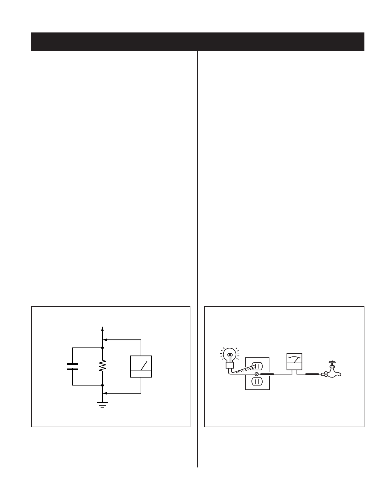
Leakage Test
The AC leakage from any exposed metal part to earth ground and from
all exposed metal parts to any exposed metal part having a return to
chassis, must not exceed 0.5 mA (500 microamperes). Leakage current
can be measured by any one of three methods.
1. A commercial leakage tester, such as the Simpson 229 or
RCA WT-540A. Follow the manufacturers’ instructions to use these
instructions.
2. A battery-operated AC milliammeter. The Data Precision 245 digital
multimeter is suitable for this job.
3. Measuring the voltage drop across a resistor by means of a VOM
or battery-operated AC voltmeter. The “limit” indication is 0.75 V,
so analog meters must have an accurate low voltage scale. The
Simpson’s 250 and Sanwa SH-63TRD are examples of passive VOMs
that are suitable. Nearly all battery-operated digital multimeters that
have a 2 VAC range are suitable (see Figure A).
How to Find a Good Earth Ground
A cold-water pipe is a guaranteed earth ground; the cover-plate retaining
screw on most AC outlet boxes is also at earth ground. If the retaining
screw is to be used as your earth ground, verify that it is at ground
by measuring the resistance between it and a cold-water pipe with an
ohmmeter. The reading should be zero ohms.
If a cold-water pipe is not accessible, connect a 60- to 100-watt troublelight (not a neon lamp) between the hot side of the receptacle and the
retaining screw. Try both slots, if necessary, to locate the hot side on the
line; the lamp should light at normal brilliance if the screw is at ground
potential (see Figure B).
To Exposed Metal
Parts on Set
Trouble Light
AC Outlet Box
Ohmmeter
AC
0.15 µF
1.5 K Ω
Voltmeter
(0.75 V)
Earth Ground
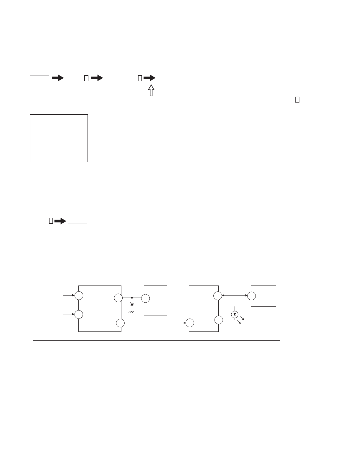
Figure A. Using an AC voltmeter to check AC leakage. Figure B. Checking for earth ground.
— 5 —
Cold-water Pipe
KV-32FV27 / 36FS13 / 36FS17 / 36FV27/ 38FS17
SELF-DIAGNOSTIC FUNCTION
Self Diagnosis
Supported model
The units in this manual contain a self-diagnostic function. If an error occurs, the STANDBY/TIMER LED will automatically begin to fl ash. The number
of times the LED fl ashes translates to a probable source of the problem. A defi nition of the STANDBY/TIMER LED fl ash indicators is listed in the
instruction manual for the user’s knowledge and reference. If an error symptom cannot be reproduced, the Remote Commander can be used to review
the failure occurrence data stored in memory to reveal past problems and how often these problems occur.
Diagnostic Test Indicators
When an error occurs, the STANDBY/TIMER LED will fl ash a set number of times to indicate the possible cause of the problem. If there is more than
one error, the LED will identify the fi rst of the problem areas.
Results for all of the following diagnostic items are displayed on screen. No error has occurred if the screen displays a “0”.
Diagnostic Item
Power does not turn on
+B overcurrent (OCP)*
+B overvoltage (OVP)*
No. of times
STANDBY/ TIMER
lamp fl ashes
Does not light
N/A
N/A
Display Result
N/A
N/A
N/A
Probable Cause Location
• Power cord is not plugged in.
• Fuse is burned out (F601). (G Board)
• H.OUT (Q502) is shorted.(A Board)
• IC1701 is shorted. (C Board)
• IC643 or T603 is open. (G Board) • Power does not come on.
Detected Symptoms
• Power does not come on.
• No Power is supplied to the TV.
• AC Power supply is faulty.
• Power does not come on.
• Load on power line is shorted
V-STOP
IK (AKB)
4 times
5 times
4:0 or 4:1
5:0 or 5:1
• +13V is not supplied. (A Board)
• IC561 is faulty. (A Board)
• Video OUT (IC561) is faulty. (A Board)
• IC355 is faulty. (A Board)
• Screen (G2) is improperly adjusted.**
* If a +B overcurrent is detected, stoppage of the vertical defl ection is detected simultaneously.
The symptom that is diagnosed fi rst by the microcontroller is displayed on the screen.
** Refer to Screen (G2) Adjustments in Section 2-4. of this manual.
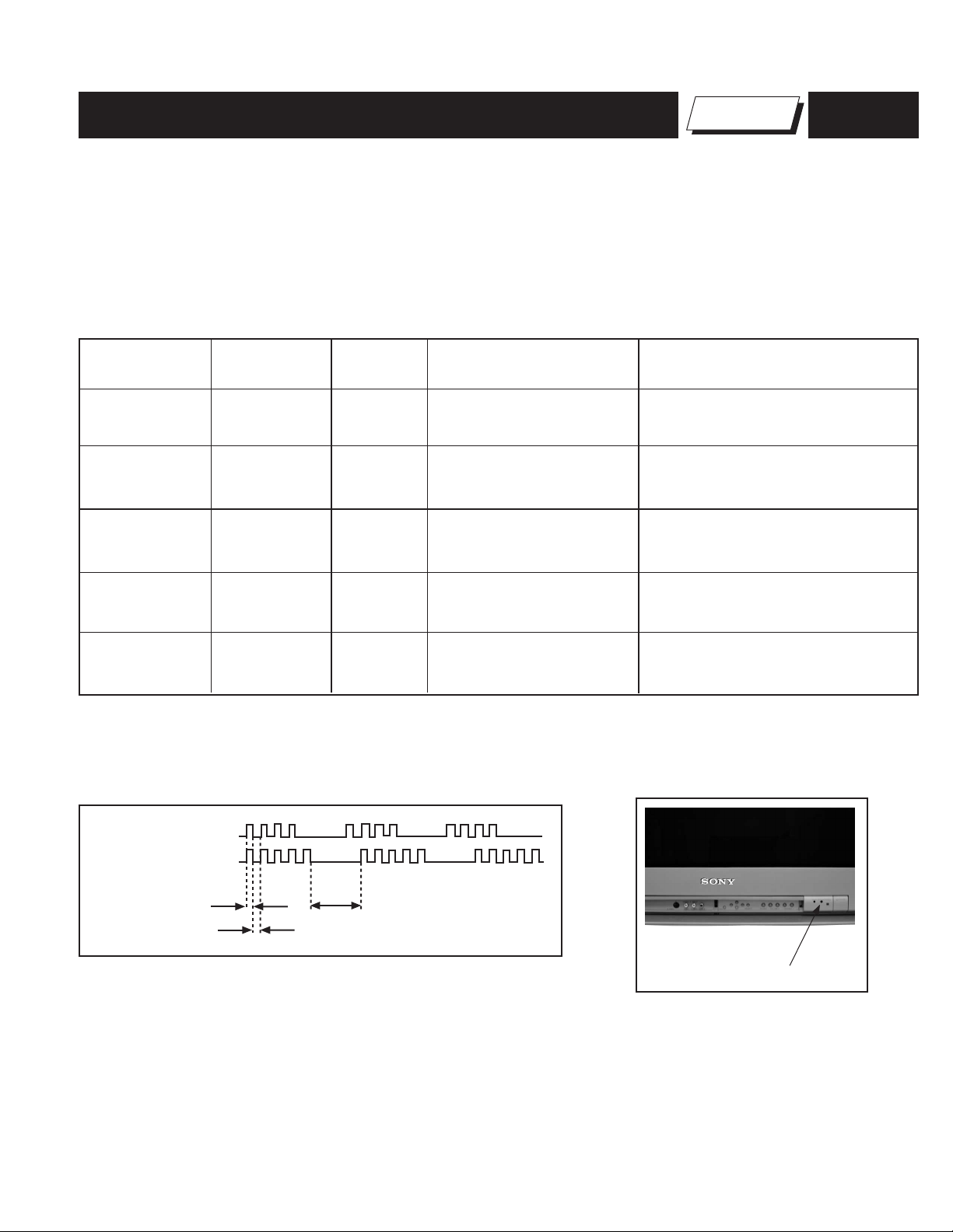
Display of Standby/Timer LED Flash Count
4 times
5 times
LED ON 0.3 sec.
LED OFF 0.3 sec.
LED OFF
3 sec.
Diagnostic Item Flash Count*
V-STOP 4 times
IK (AKB) 5 times
• Has entered standby state after horizontal raster.
• Vertical defl ection pulse is stopped.
• Power line is shorted or power supply is stopped.
• No raster is generated.
• CRT Cathode current detection reference
• Pulse output is small.
Standby/Timer LED
*One fl ash count is not used for self-diagnostic.
Stopping the Standby/Timer LED Flash
Turn off the power switch on the TV main unit or unplug the power cord from the outlet to stop the STANDBY/TIMER LAMP from fl ashing.
— 6 —
KV-32FV27 / 36FS13 / 36FS17 / 36FV27/ 38FS17
Self-Diagnostic Screen Display
For errors with symptoms such as “power sometimes shuts off” or “screen sometimes goes out” that cannot be confi rmed, it is possible to bring up
past occurrences of failure on the screen for confi rmation.
To Bring Up Screen Test
In standby mode, press buttons on the Remote Commander sequentially, in rapid succession, as shown below:
Display
Self-diagnostic Screen Display
Channel 5 Sound Volume - Power ON
Note that this differes from entering the Service Mode (Sound volume
+
).
SELF DIAGNOSIS
2: +B OCP N/A
3: +B OVP N/A
4: VSTOP 0
5: AKB 1
Numeral “0” means that no fault was detected.
Numeral “1” means a fault was detected one time only.
101: WDT 24
Handling of Self-Diagnostic Screen Display
Since the diagnostic results displayed on the screen are not automatically cleared, always check the self-diagnostic screen during repairs. When you
have completed the repairs, clear the result display to “0”.
Unless the result display is cleared to “0”, the self-diagnostic function will not be able to detect subsequent faults after completion of the repairs.
Clearing the Result Display
To clear the result display to “0”, press buttons on the Remote Commander sequentially when the diagnostic screen is displayed, as shown below:
Channel
8
ENTER
Quitting the Self-Diagnostic Screen
To quit the entire self-diagnostic screen, turn off the power switch on the Remote Commander or the main unit.
Self-Diagnostic Circuit
FROM
C BOARD
IC1701 PIN 6
A BOARD
FROM
IC501
PIN 1
A BOARD
IC355
Y/CHROMA JUNGLE
21
IK IN
18
HP/PROTECT
VM
SDA
15
35
A BOARD
IC561
V. OUT
3
REF
A BOARD
IC001
SYSTEM
IO-BDATN
O-TIMELED
27
IO-SDAT
26
59
A BOARD
IC1002
MEMORY
5
BDA
DISPLAY
+B overcurrent (OCP) Occurs when an overcurrent on the +B (135V) line is detected by pin 18 of IC355 (A Board). If the voltage of pin 18 of
IC355 (A Board) is less than 1V when V.SYNC is more than seven verticals in a period, the unit will automatically turn off.
+B overvoltage (OVP) Occurs when the feedback circuit from +B opens IC643 or T603 or any other associated feedback components.
V-STO P Occurs when an absence of the vertical defl ection pulse is detected by pin 15 of IC355 (A Board). Power supply will
shut down when waveform interval exceeds 2 seconds.
IK (AKB) If the RGB levels* do not balance within 2 seconds after the power is turned on, this error will be detected by IC355
(A Board). TV will stay on, but there will be no picture.
NOTE:
Watch Dog Timer Indicates how many times the Watch Dog Timer functions have been activated. Whenever micro is reset by the Watch
Dog Timer, this number is incremented. Maximum number is 255.
* Refers to the RGB levels of the AKB detection Ref pulse that detects 1K.
— 7 —
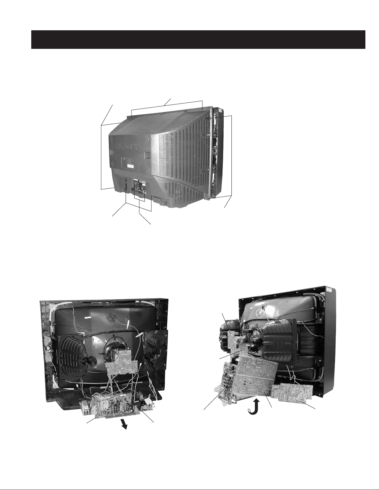
1-1. REAR COVER REMOVAL
KV-32FV27 / 36FS13 / 36FS17 / 36FV27/ 38FS17
SECTION 1: DISASSEMBLY
* Screws(+BVTP 4x16)
* Screws
(+BVTP 4x16)
* Screws (+BVTP 4x16)
* (+BVTP 4 x 16) Screw Legend:
KV-32FV27 = 14 Screws Total
KV-36FV27 = 16 Screws Total
KV-36FS13/ 36FS17 / 38FS17= 15 Screws Total
* Screws (+BVTP 4x16)
2 Screws (+BVTP 3x12)
1-2. CHASSIS ASSEMBLY REMOVAL 1-3. SERVICE POSITION
C Board
WA Board
A Board
Chassis Assembly
Claw
UY Board
(KV-36FS13/36FS17/ 38FS17 ONLY)
UX Board
(KV-32FV27/36FV27 ONLY)
G Board
— 8 —
1-4. PICTURE TUBE REMOVAL
WARNING: BEFORE REMOVING THE ANODE CAP
High voltage remains in the CRT even after the power is disconnected. To avoid electric shock,
discharge CRT before attempting to remove the anode cap. Short between anode and CRT
coated earth ground strap.
KV-32FV27 / 36FS13 / 36FS17 / 36FV27/ 38FS17
Coated
Earth
Ground
Strap
10
6
5
8
9
4
1
1. Discharge the anode of the CRT and remove the anode cap.
7
2. Unplug all interconnecting leads from the defl ection yoke, neck
assembly, degaussing coils and CRT grounding strap.
3. Remove the C and WA Board from the CRT.
2
4. Remove the chassis assembly.
5. Loosen the neck assembly fi xing screw and remove.
6. Loosen the defl ection yoke fi xing screw and remove.
3
7. Place the set with the CRT face down on a cushion and remove the
degaussing coil holders.
8. Remove the degaussing coils.
9. Remove the CRT grounding strap and spring tension devices.
10. Unscrew the four CRT fi xing screws [located on each CRT corner]
and remove the CRT [Take care not to handle the CRT by the
neck].
ANODE CAP REMOVAL PROCEDURE
WARNING: High voltage remains in the CRT even after the power is disconnected. To avoid electric shock, discharge the CRT before attempting to
remove the anode cap. Short between anode and coated earth ground strap of CRT.
NOTE: After removing the anode cap, short circuit to either the metal chassis, CRT shield, or carbon painted on the CRT.
REMOVAL PROCEDURES
c
b
a
Anode Button
Turn up one side of the rubber cap
1
inthe direction indicated by arrow
a
.
2
Use your thumb to pull the rubber
cap fi rmly in the direction indicated
by arrow
b
.
HOW TO HANDLE AN ANODE CAP
1. Do not use sharp objects which may cause damage to the surface of the anode
cap.
2. To avoid damaging the anode cap, do not squeeze the rubber covering too hard.
A material fi tting called a shatter-hook terminal is built into the rubber.
3. Do not force turn the foot of the rubber cover. This may cause the shatter-hook
terminal to protrude and damage the rubber.
— 9 —
3
When one side of the rubber cap separates from
the anode button, the anode cap can be removed
by turning the rubber cap and pulling it in the
direction of arrow
c
.
SECTION 2: SET-UP ADJUSTMENTS
KV-32FV27 / 36FS13 / 36FS17 / 36FV27/ 38FS17
The following adjustments should be made when a complete
realignment is required or a new picture tube is installed.
These adjustments should be performed with rated power supply
voltage unless otherwise noted.
The controls and switch should be set as follows unless otherwise
noted:
PICTURE control: normal
BRIGHTNESS control: normal
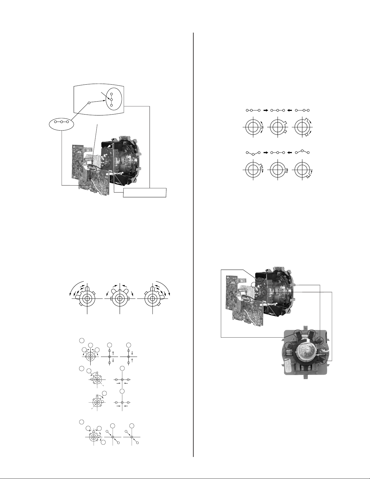
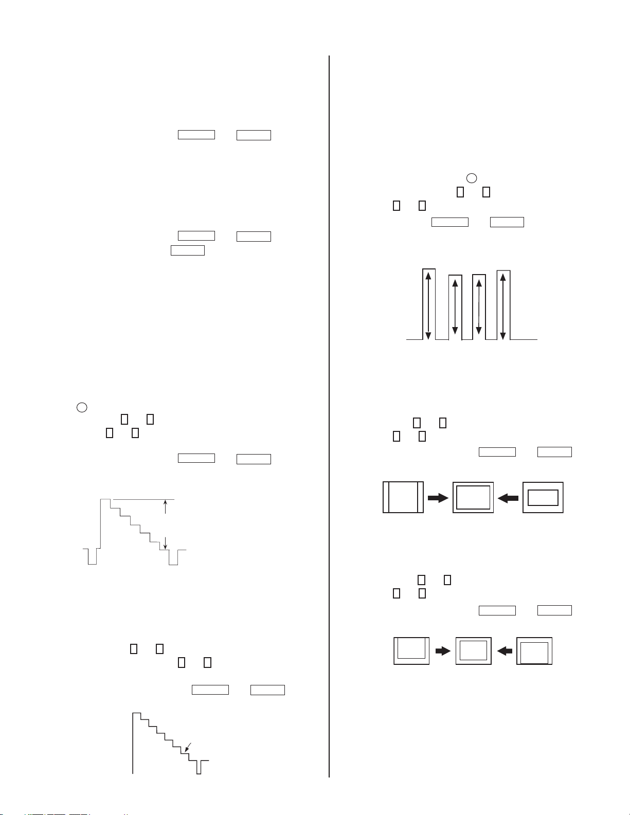
2-1. BEAM LANDING
Preparation:
• Input a white pattern signal.
• Face the picture tube in an East or West direction to reduce the
infl uence of geomagnetism.
NOTE: Do not use the hand degausser because it magnetizes the
CRT .
1. Input white pattern from pattern generator.
2. Loosen the defl ection yoke mounting screw, and set the purity control
to the center as shown below:
Perform the adjustments in order as follows:
1. Beam Landing
2. Convergence
3. Focus
4. Screen (G2)/White Balance
Note Test Equipment Required:
1. Color Bar Pattern Generator
2. Degausser
3. DC Power Supply
4. Digital Multimeter
5. Oscilloscope
6. CRT Analyzer
Purity Control
3. Input green pattern from pattern generator.
4. Move the defl ection yoke backward, and adjust with the purity control
so that green is in the center and red and blue are even on both
sides.
Red
Blue
Green
6. Switch over the raster signal to red and blue and confi rm the
condition.
7. When the position of the defl ection yoke is determined, tighten it with
the defl ection yoke mounting screw.
8. When landing at the corner is not right, adjust by using the disk
magnets.
Purity control
corrects this area
a
Disk magnets
or rotatable disk
magnets correct
these areas (a-d)
Deflection yoke positioning
corrects these areas
b
d
cd
b
a
c
5. Move the defl ection yoke forward, and adjust so that the entire screen
becomes green.
— 10 —
KV-32FV27 / 36FS13 / 36FS17 / 36FV27/ 38FS17
2-2. CONVERGENGE
Preparation:
• Perform FOCUS, V. LIN and V. SIZE adjustments.
• Set BRIGHTNESS control to minimum.
• Input dot pattern.
Center dot
R
G
B
RV1761 V.STAT
R G B
V.STAT magnet
VERTICAL AND HORIZONTAL STATIC
CONVERGENCE
1. Adjust V. STAT magnet to converge red, green and blue dots in the
center of the screen (Vertical movement).
Tilt the V. STAT magnet and adjust static convergence to open or
close the V. STAT magnet.
OPERATION OF BMC (HEXAPOLE) MAGNET
The respective dot positions resulting from moving each magnet interact,
so perform adjustment while tracking.
1. Use the V.STAT tabs to adjust the red, green, and blue dots so they
line up at the center of the screen (move the dots in a horizontal
direction).
G
R
R
G
G
B
B
BRGB
R
B
G
R
G
R
B
Y SEPARATION AXIS CORRECTION MAGNET
ADJUSTMENT
1. Input cross-hatch pattern, adjust PICTURE to minimum and
BRIGHTNESS to normal.
2. Adjust the defl ection yoke upright so it touches the CRT.
3. Adjust so that the Y separation axis correction magnet on the neck
assembly is symmetrical from top to bottom (open state).
2. When the V. STAT magnet is moved in the direction of arrow a and b,
red, green, and blue dots move as shown below:
1
a
b
2
a
3
b
a
b
B
G
R
b
a
R
G
b
a
RGB
b
BGR
a
B
b
B
G
R
b
G
R
V.S TAT
BMC MAGNET
PURITY
4. Return the defl ection yoke to its original position.
— 11 —
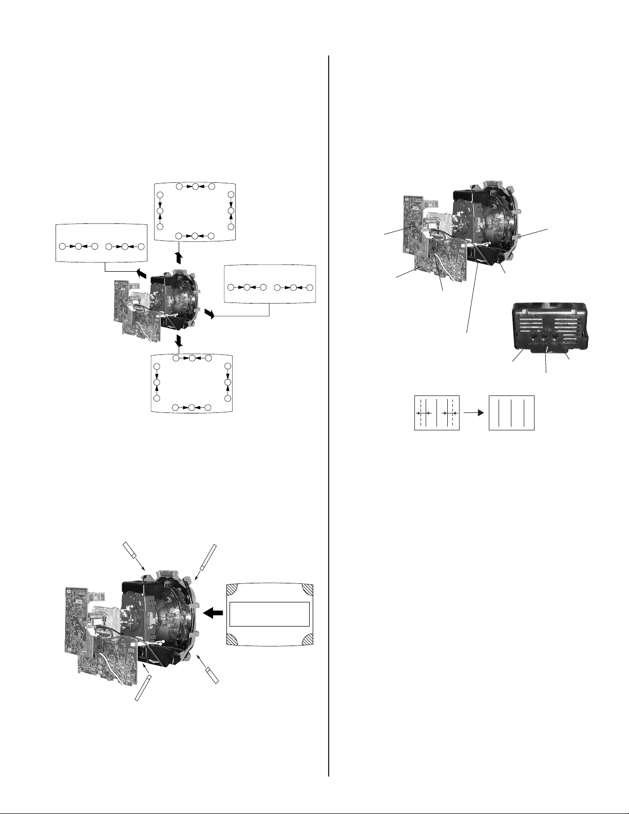
KV-32FV27 / 36FS13 / 36FS17 / 36FV27/ 38FS17
DYNAMIC CONVERGENCE ADJUSTMENT
Before starting, perform Vertical and Horizontal Static Convergence
Adjustment.
1. Slightly loosen defl ection yoke screw.
2. Remove defl ection yoke spacers.
3. Move the defl ection yoke for best convergence as
shown below:
G
B
R
G
B
BGR
B
G
R
R
R
B
G
R
B
G
BGR
R
GB
TLH PLATE ADJUSTMENT
Preparation:
• Input crosshatch pattern.
• Adjust Picture Quality to standard, Picture and Brightness to 50%,
and Other to standard.
• Adjust the Horizontal Convergence of red and blue dots by tilting the
TLH plate on the defl ection yoke.
C Board
WA Board
TLH Plate
RV1761
V.S TAT
XCV
Y Magnet
R
B
G
R
B
R
G
B
R
G
B
G
4. Tighten the defl ection yoke screw.
5. Install the defl ection yoke spacers.
SCREEN-CORNER CONVERGENCE
1. Affi x a permalloy assembly corresponding to the misconverged areas:
b
a
ba
a-d: screen-corner
misconvergence
cd
TLV
BR
(R) (B)
RB
(B) (R)
TLH+
TLH-
H-TRP
YCH
1. Adjust XCV core to balance X axis.
2. Adjust YCH VR to balance Y axis.
3. Adjust vertical red and blue convergence with V.TILT (TLV VR).
Perform adjustments while tracking items 1 and 2.
4. Adjust Y MAGNET to correct V.BOW Geometery Distortion.
5. Adjust H-TRP to correct H.Trapezoid Geometry Distortion.
After adjusting items 4 and 5, confi rm overall geometry again.
c
d
— 12 —
KV-32FV27 / 36FS13 / 36FS17 / 36FV27/ 38FS17
2-3. FOCUS
1. Input monoscope signal.
2. Set user controls to normal.
3. Set video mode to STANDARD.
4. Set the PICTURE to maximum.
5. Adjust at 325 Mark for best center/corner focus balance.
6. Receive an entire white signal. Make sure Magenta Ring is at an
acceptable level.
Focus
Screen (G2)
325 MARK
35
35 MARK
CENTER
CIRCLE
325
2-5. WHITE BALANCE ADJUSTMENTS
NO.
24
25
26
27
28
29
36
Disp.
RDRV
GDRV
BDRV
RCUT
GCUT
BCUT
SBRT
Item
Red Drive
Green Drive
Blue Drive
Red Cut-off
Green Cut-off
Blue Cut-off
Sub Bright
1. Set program palette to STANDARD and push RESET.
2. Input an entire white signal.
3. Set to Service Adjustment Mode.
4. Set the PICTURE and BRIGHT to minimum.
5. Adjust with SBRT if necessary.
6. Set RCUT to “14”.
7. Select GCUT and BCUT with
8. Adjust with
3
and 6 for the best white balance.
1
and 4 .
9. Set the PICTURE and BRIGHT to maximum.
10. Select GDRV and BDRV with
11. Adjust with
3
and 6 for the best white balance.
12. Write into the memory by pressing
1
and 4 .
MUTING
13. Repeat steps 1-12 for GDR4, BDR4, GCU4 and BCU4 using Video 4
input.
*Use values from Sub Contrast Adjustments
All Models
then
*
31
31
14:Fix
7
7
7
ENTER
.
2-4. SCREEN (G2)
1. Input dot pattern from the pattern generator.
2. Set the user controls to NORMAL.
3. Attach the G2-Jig to the C Board.
4. Adjust RCUT, GCUT, BCUT, and SBRT in service mode with an
oscilloscope so that voltages on the red, green, and blue cathodes
are 170 ± 2.0 VDC.
5. Observe the screen and adjust SCREEN (G2) VR to obtain the faintly
visible background of dot signal.
6. Push the TEST + JUMP (+ Channel) to cut off the signal. The screen
should be bright or dark. Brightness of raster must be increased
when adjusting.
7. Adjust screen VR until the screen is slightly cut off, or scarcely lights
up. A signal cannot be seen when the brightness of the raster is
high.
8. Push the JUMP again to release the cut off.
170 ± 2.0 VDC
pedestal
NOTE: White Balance should be adjusted after
Sub Contrast because RDRV is also used in Sub
Contrast Adjustment (See Page 22).
GND
— 13 —
KV-32FV27 / 36FS13 / 36FS17 / 36FV27/ 38FS17
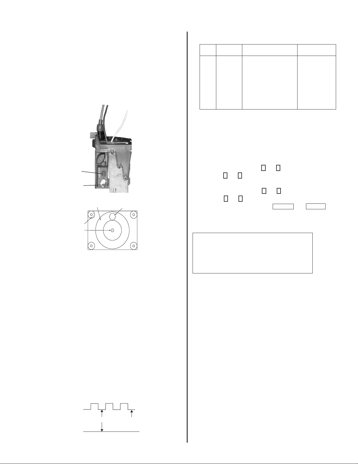
SECTION 3: SAFETY RELATED ADJUSTMENTS
3-1. X R530, R531 CONFIRMATION METHOD
(HOLD-DOWN CONFIRMATION) AND
READJUSTMENTS
Always perform the following adjustments when replacing the following
components marked with a
Part Replaced ( )
R387, R550, R529, R530,
R531, R532, R533, D519,
Y
mark on the schematic diagram:
Adjustment ( )
HV HOLD-DOWN
R530,R531
D520, D521, IC501, C531,
C532, T503, IC351, Q301,
R356, R359, R361,
D302.....................A Board
IC643, R661.........G Board
PREPARATION BEFORE CONFIRMATION
1. Using a Variac, apply AC input voltage: 120+2.0/-0.0 VAC.
2. Turn the POWER switch ON.
3. Input a white signal and set the PICTURE and BRIGHT controls to
maximum.
4. Confi rm that the voltage of more than 23.0 VDC appears between
TP85 and ground on the A Board.
HOLD-DOWN OPERATION CONFIRMATION
1. Connect the current meter between Pin 11 of the FBT (T503) and the
PWB land where Pin 11 would normally attach (See Figure 1).
2. Input a dot signal and set PICTURE and BRIGHTNESS to minimum:
IABL = 2175 + 100/ -325 µA.
3. Confi rm the voltage of A Board TP91 is 135 ± 1.5 VDC.
4. Connect the digital voltmeter and the DC power supply to TP85 and
ground (See Figure 1).
5. Increase the DC power voltage gradually until the picture blanks out.
6. Turn DC power source off immediately.
7. Read the digital voltmeter indication (standard = 27.24 +0.0 / -0.1
VDC) (KV-32FV27 ONLY), (standard = 27.24 ± 0.1 VDC) (ALL
EXCEPT KV-32FV27).
8. Input a white signal and set PICTURE and BRIGHTNESS to
maximum: IABL = 2175 + 100/ -325 µA.
9. Repeat steps 4 to 7.
HOLD-DOWN READJUSTMENT
If the setting indicated in Step 2 of Hold-Down Operation Confi rmation
cannot be met, readjustment should be performed by altering the
resistance value of R530, R531 component marked with
digital multimeter
+
-
TP85
R530
R531
DC Power Supply
TP85
+
-
Figure 1
T503
FBT
FBT
ammeter
3mA DC range
A
+
-
X
.
3-2. B+ VOLTAGE CONFIRMATION AND
ADJUSTMENT
Always perform the following adjustments when replacing the following
components, which are marked with
the G Board:
G BOARD: IC643, R661
1. Using a Variac, apply AC input voltage: 130 + 2.0/-0.0 VAC
2. Input a monoscope signal.
3. Set the PICTURE control and the BRIGHT control to
initial reset value.
4. Confi rm the voltage of G Board CN641 between pin to ground is
less than 136.5 VDC.
5. If step 4 is not satisfi ed, replace the R661 on G Board and repeat
the above steps.
Y
on the schematic diagram on
— 14 —
KV-32FV27 / 36FS13 / 36FS17 / 36FV27/ 38FS17
SECTION 4: CIRCUIT ADJUSTMENTS
ELECTRICAL ADJUSTMENTS BY REMOTE COMMANDER
Use the Remote Commander (RM-Y180, RM-Y181, RM-Y182) to perform the circuit adjustments in this section.
Test Equipment Required: 1. Pattern generator 2. Frequency counter 3. Digital multimeter 4. Audio oscillator
4-1. SETTING THE SERVICE ADJUSTMENT
MODE
1. Standby mode (Power off).
2. Press
Display
Channel 5 Sound Volume + Power
SERVICE ADJUSTMENT MODE ON
Item
order
0
TV
Item
data
7
SERVICE
Mode
Disp.
(Item)
VP
HSIZ
3. The CRT displays the item being adjusted.
4. Press
5. Press
6. Press
2
on the Remote Commander to select the item.
or
1
3
or 6 on the Remote Commander to change the data.
MUTING
then
to write into memory.
ENTER
SERVICE ADJUSTMENT MODE MEMORY
Item
Item
order
data
7
SERVICE
0
TV
MUTING
ENTER
Green
Red
on the Remote Commander to initialize.
Item
data
7
WRITE
TV
Carry out step 7 when adjusting
IDs 0 to 7 and when replacing and
adjusting IC002.
7. Press
8
then
Disp.
(Item)
VP
HSIZ
Disp.
(Item)
VP
HSIZ
ENTER
Item
order
0
4-2. MEMORY WRITE CONFIRMATION
METHOD
1. After adjustment, pull out the plug from the AC outlet, then replace
the plug in the AC outlet again.
2. Turn the power switch ON and set to Service Mode.
3. Call the adjusted items again to confi rm they were adjusted.
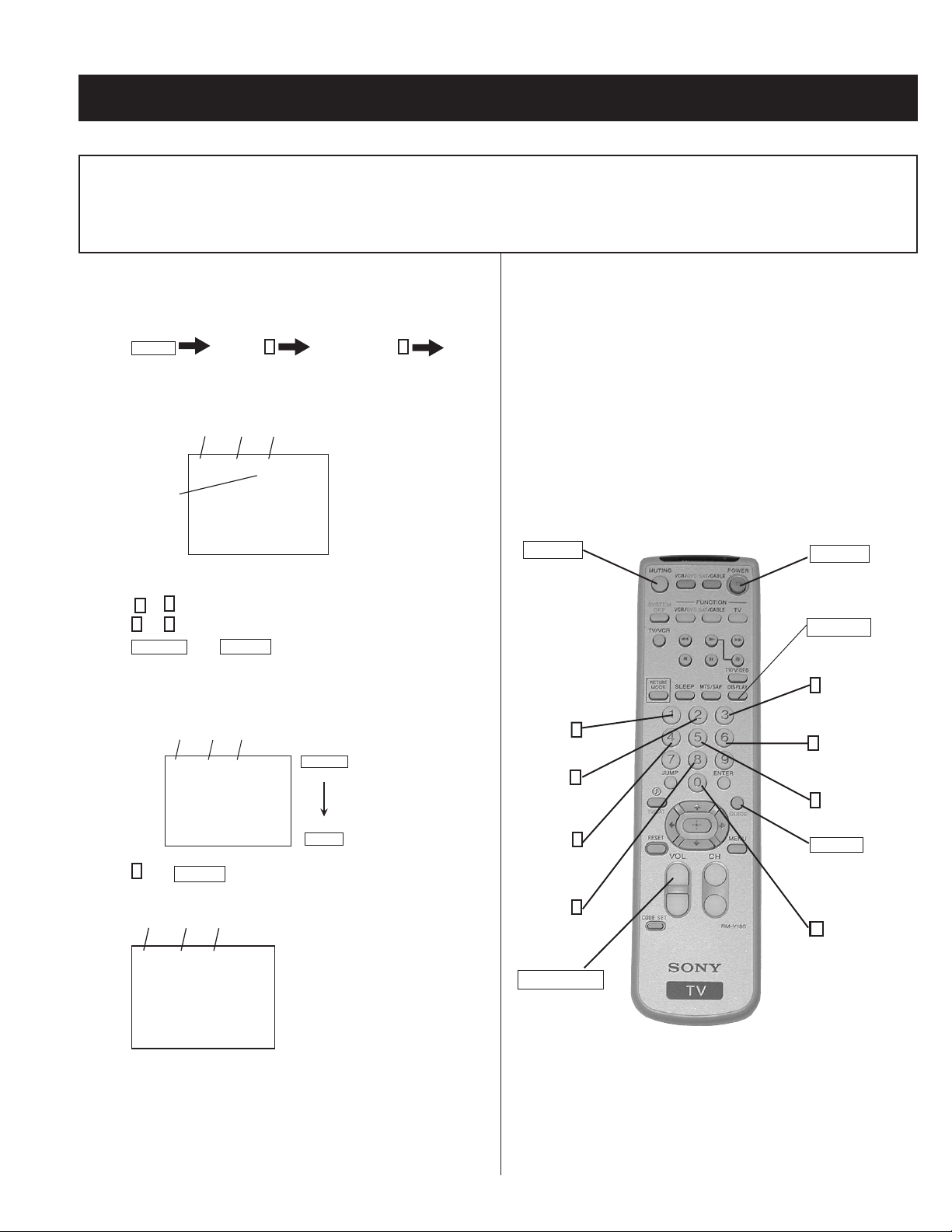
4-3. REMOTE ADJUSTMENT BUTTONS AND
INDICATORS
MUTING
(Enter into
memory
1
Disp. (Item up)
2
(Device Item Up)
4
Disp. (Item down)
8
(Initialize)
VOLUME (+)
(Service Mode)
POWER
(Service Mode)
DISPLAY
(Service Mode)
3
Item (Data up)
6
Item (Data down)
5
(Device item down)
ENTER
(Enter into
memory
0
(Remove from
memory)
8. DO NOT turn off set until SERVICE appears.
RM-Y182
— 15 —
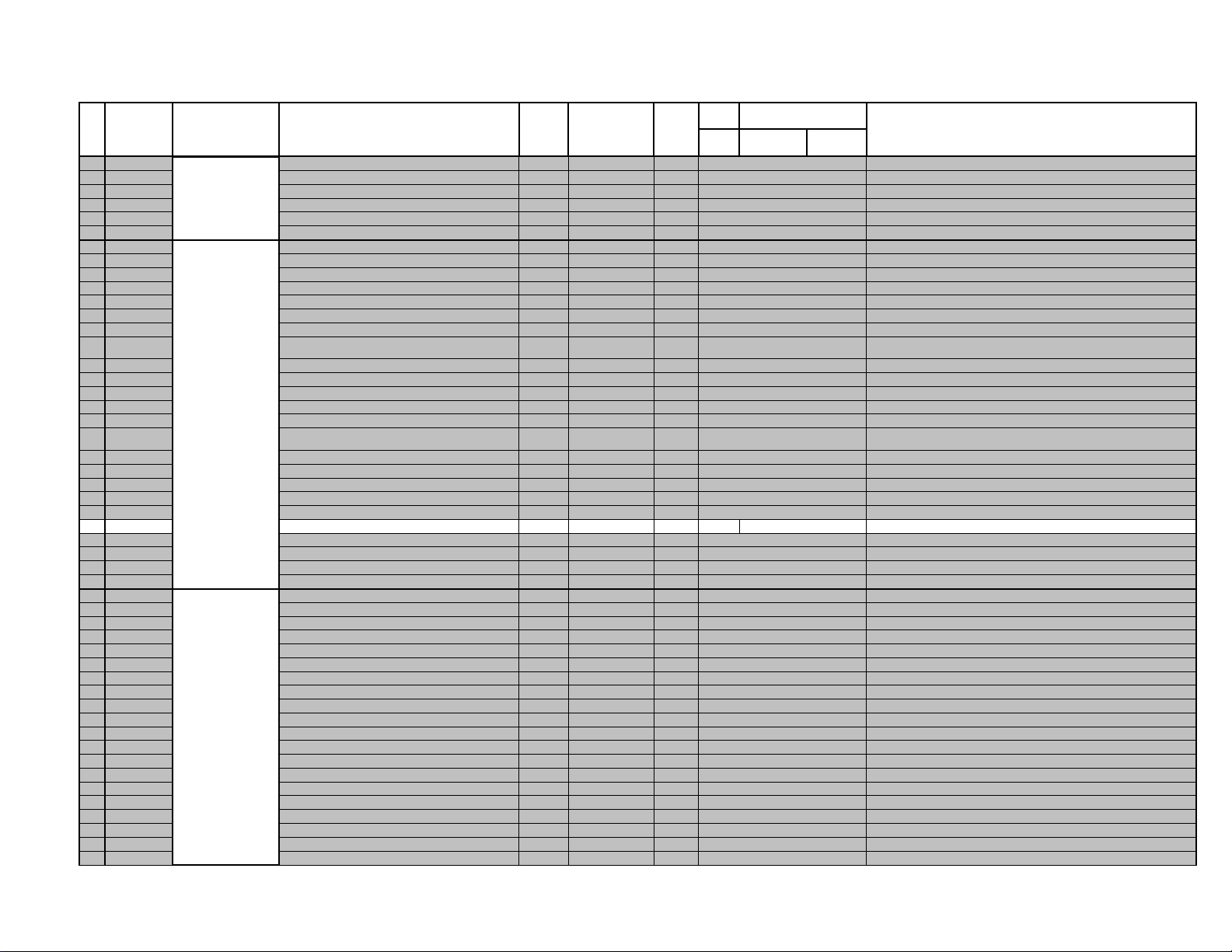
4-4. ADJUSTMENT ITEMS (1 OF 6)
f
KV-32FV27 / 36FS13 / 36FS17 / 36FV27 / 38FS17
10
11
12
13
14
15
16
17
18
19
20
21
22
23
24
25
26
27
28
29
30
31
32
33
34
35
36
37
38
39
40
41
42
43
44
45
46
47
0
1
2
3
4
5
6
7
8
9
Register
Name
HPOS
HSIZ
VBOW
VANG
TRAP
PAMP
UCPN
LCPN
VSIZ
VPOS
VLIN
VSCO
VZOM
EHT
ASP
ASP1
SCRL
HBSW
LBLK
RBLK
HDW
EWDC
LVLN
UVLN
RDRV
GDRV
BDRV
RCUT
GCUT
BCUT
RDR4
GDR4
BDR4
RCU4
GCU4
BCU4
SBRT
RON
GON
BON
AXPL
CBPF
COFF
TSSP
TSPF
VSSP
VSPF
YSSP
VP
CXA2131AS
Description Data Adj/Fix Initial 32" 36"/38" Comments
H-Position
H-Size
AFC Bow
AFC Angle
Trapezium Adjustment
Pin Compensation
Upper Corner Pin
Lower Corner Pin
V-Size
V-Position
V-Linearity
S-Correction
16:9 CRT Zoom Mode On/Off
Vertical Size High Voltage Correction
Aspect Ration Control 4:3 Mode
Aspect Ration Control 16:9 Mode
16:9 Vertical Scroll During Zoom
H Blanking Switch
Left Blanking
Right Blanking
H Drive Pulse Width
EW/DC Display 4x3 on 16x9 CRT
Picture Bottom Lin Adjust
Picture Top Lin Adjust
Red Drive
Green Drive
Blue Drive
Red Cutoff
Green Cutoff
Blue Cutoff
Video 4 Red Drive
Video 4 Green Drive
Video 4 Blue Drive
Video 4 Red Cutoff
Video 4 Green Cutoff
Video 4 Blue Cutoff
Sub Brightness
Red Off
Green Off
Blue Off
Axis PAL
Chroma BPF On/Off
Color On/Off
Sub Sharpness for TV Input
Sharpness fo for TV Input
Sub Sharpness for Video Input
Sharpness fo for Video Input
Sub Sharpness for YUV Input
Range Data FV FS FV
0-63
0-63
0-15
0-15 Adj
0-15
0-63
0-63
0-63
0-63
0-63
0-15
0-15
0,1
0-15
0-63
0-63
0-63
0,1
0-15
0-15
0,1
0,1
0-15
0-15
0-63
0-63
0-63
0-15
0-15
0-15
0-63
0-63
0-63
0-15
0-15
0-15
0-31 Adj
0,1
0,1
0,1
0,1
0,1
0,1
0-15
0,1
0-15
0,1
0-15
Adj 77 7
Adj 10 10 10
Adj 66 6
55 5
Adj 66 6
Adj 32 32 32
Adj 36 36 36
Adj 36 36 36
Adj 00 0
Adj 31 31 31
Adj 77 7
Adj 77 7
FIX 0 0
FIX 4 4
FIX 47 47
FIX 47 47
FIX 31 31
FIX 1 1
FIX 15 15
FIX 0 0
FIX 1 1
FIX 0 0
Adj 00
Adj 00
Adj 31 31 48 54
Adj 31 31
Adj 31 31
FIX 7 14
Adj 77
Adj 77
Adj 31 31 54
Adj 31 31
Adj 31 31
FIX 7 14
Adj 77
Adj 77
FIX 1 1
FIX 1 1
FIX 1 1
FIX 0 0
FIX 1 1
FIX 0 0
Fix by model 6 6 5 6
FIX 1 1
Fix by model 7 7 5 7
FIX 1 1
Fix by model 7 7 6 7
adjust to
15
IRE
cutof
adjust to IRE cutoff
0: 2ms delay, 63: 2ms advance
EW DC bias, 0: -0.5V, 31: 0V, 63: +0.5V
0: top/bottom delay 900ns, 7: center, 15: top/bottom advance 900ns
0: top delay/bottom advance 650ns, 7: center,
15: top advance/bottom delay 650ns
0: 1.5ms advance, 15: 1.5ms delay
0: 0.15Vpp, 31: 0.7Vpp, 63: 1.3Vpp
0: -0.4V, 63: +0.4V
0: -0.4V, 63: +0.4V
0: -15%, 31: 0%, 63: +15%
0: -0.1V, 31: 0V, 63: +0.1V
0: 85% top enlarged, 7: 100% top normal, 15: 115% top compressed
0: 0V added to VD, 15: 100mVpp added to VD
0: Zoom Off, 1: Zoom On
(top/bottom cut by 25% when ASPECT=31, RGB blanked in this interval)
0: Picture adjusted 0%, 15: Picture Adjusted -5%
0: 75%(16x9 CRT Full), 31: 100%(4x3 CRT Full), 63: 110%
0: 75%(16x9 CRT Full), 31: 100%(4x3 CRT Full), 63: 110%
0: Scrolled toward top 32H, 63: Scrolled toward bottom 32H
0: OFF, 1: ON
0: +1.2ms, 7: Center, 15: -1.2ms
0: +1.2ms, 7: Center, 15: -1.2ms
0: Normal Mode (25ms), 1: Narrow Pulse Width
0: OFF, 1: ON
0: 100%, 15: 85% Picture top compressed
0: 100%, 15: 85% Picture bottom compressed
0: 1.5Vpp, 63: 3.0Vpp Red Signal Output
0: 1.5Vpp, 63: 3.0Vpp Greem Signal Output
0: 1.5Vpp, 63: 3.0Vpp Blue Signal Output
0: 3.5mA IK, 7: 13mA IK, 15: 22.7mA IK
0: 3.5mA IK, 7: 13mA IK, 15: 22.7mA IK
0: 3.5mA IK, 7: 13mA IK, 15: 22.7mA IK
0: 1.5Vpp, 63: 3.0Vpp Red Signal Output
0: 1.5Vpp, 63: 3.0Vpp Greem Signal Output
0: 1.5Vpp, 63: 3.0Vpp Blue Signal Output
0: 3.5mA IK, 7: 13mA IK, 15: 22.7mA IK
0: 3.5mA IK, 7: 13mA IK, 15: 22.7mA IK
0: 3.5mA IK, 7: 13mA IK, 15: 22.7mA IK
Sub Brightness
0:OFF, 1:ON
0:OFF, 1:ON
0:OFF, 1:ON
0: Normal Axis, 1: Forced PAL Asix
0: BPF OFF, 1: BPF ON
0: Chroma OFF, 1: Chroma ON
0=-12dB, 7=+3.5dB, 15=+9dB
0=2.5MHZ, 1=3.0MHz
0=-12dB, 7=+3.5dB, 15=+9dB
0=2.5MHZ, 1=3.0MHz
0=-12dB, 7=+3.5dB, 15=+9dB
— 16 —
ADJUSTMENT ITEMS (2 OF 6)
KV-32FV27 / 36FS13 / 36FS17 / 36FV27 / 38FS17
48
49
50
51
52
53
54
55
56
57
58
59
60
61
62
63
10
11
12
13
14
15
16
17
18
19
20
21
22
23
0
1
2
3
4
5
6
0
1
2
0
1
2
3
4
5
6
7
8
9
Register
Name
YSPF
AXNT
PREL
DCT
ABLM
FSC
HOSC
VSS
HSS
HMSK
VTMS
AFC
REFP
VBSW
BKOF
AGN2
SREF
BBLP
BBHP
SVOL
SBAL
SBAS
STRE
SPCA
CENA
INPA
COUT
YAPS
NSDS
MSS
EXAD
PECS
EXCS
CPP
HDP
CDL
DYCO
DYGA
DCCO
DCGA
YNRK
YNRI
YNRL
CNRK
CNRI
CNRL
ID1O
ID1W
ID1N
CLK
VP
CXA2131AS
AP
BH3868
SRS
TDA7464
3D COMB
uPD64082
Description Data Adj/Fix Initial 32" 36"/38" Comments
Range Data FV FS FV
Sharpness fo for YUV Input
Axis NTSC
Pre/Overshoot Ratio
DC Transmission Ratio
ABL Mode
FSC Output On/Off
H VCO Frequency Adjustment
Vsync Slice Level
Hsync Slice Level
Macrovision Countermeasure
Select Signal VTIM Pin
AFC
REFP
VBLK Width Control
ABL Signal Detection Level
Aging Mode 2 - Black Output Mode
Surround Effect
BBE Low PAss
BBE High Pass
Sub Volume
Sub Balance
Sub Bass
Sub Treble
SRS Space Attenuation
SRS Center Attenuation
Input Attenuation
Chroma Signal Gain / BPF
Y V-Compensation/Peaking
Standard/Non-Standard Processing
Inter-frame/Inter-line Mode
External ADC Insert
Pedestal Error Correction
C sync Input
Y ADC Amplitude/Clamp Method
H Phase Fine Adjustment
C Output Delay Fine Adjustment
Y Moving Coring Level
Y Moving Coring Gain
C Moving Coring Level
C Moving Coring Gain
YNR Non-linear Filter Gain
YNR Non-linear Filter Convergence
YNR Non-linear Filter Limit Level
CNR Non-linear Filter Gain
CNR Non-linear Filter Convergence
CNR Non-linear Filter Limit Level
ID-1 Superimpose Signal
Specifies bit A1 of Word 0
Spedifies bit A2 of Word 0
CLK8 Pin Output
0,1
0,1
0,1
0,1
0,1
0,1
0-15
0,1
0,1
0,1
0-3
0-3
0,1
0-3
0,1
0,1
0-15
0-15
0-15
0-15
0-15
0-15
0-15
0-63
0-63
0-127
0-3
0-3
0-3
0-3
0,1
0-3
0-3
0-3
0-7
0-7
0-15
0-15
0-15
0-15
0,1
0,1
0-3
0,1
0,1
0-3
0,1
0,1
0,1
0,1
FIX 1 1
FIX 0 0
FIX 1 1
FIX 1 1
FIX 1 1
FIX 1 1
FIX 12 12
FIX 0 1
FIX 0 1
FIX 1 1
FIX 0 0
FIX 0 0
FIX 0 0
FIX 0 0
FIX 0 0
FIX 0 0
FIX 7 7
FIX 5 5
FIX 3 3
FIX 7 7
FIX 7 7
Fix by model 5 5 8 5
Fix by model 3 5 8 5
FIX 0 0
FIX 0 0
FIX 3 3
FIX 3 3
FIX 3 3
FIX 0 0
FIX 0 0
FIX 0 0
FIX 0 0
FIX 1 1
FIX 0 0
FIX 3 3
FIX 5 5
FIX 2 2
FIX 10 10
FIX 2 2
FIX 9 9
FIX 1 1
FIX 0 0
FIX 1 1
FIX 1 1
FIX 0 0
FIX 1 1
FIX 0 0
FIX 0 0
FIX 0 0
FIX 1 1
0=2.5MHZ, 1=3.0MHz
0: Japan Axis, 1: US Axis
0: 1:1, 1: 2:1
0:100%, 1:85%
0:Picture ABL, 1:Picture/Brightness ABL
0: FSC output OFF, 1: FSC output ON
0: Low, 15: High (40 Hz Steps)
0: 1/3 from sync tip, 1: 1/4 from sync tip
0: 1/3 from sync tip, 1: 1/4 from sync tip
0: Off, 1: ON
0: V retrace timing, 1: Hsync signal, 2: Vsync signal, 3: don't use
0: High Gain, 1: Medium Gain, 2: don’t use, 3: Extremely low gain
0: R=20H/G=21H/B=22H, 1: R=23H/G=24H/B=25H
0: 9H from B, 1: 10H from B, 2: 11H from B, 3:12H from B
(When JUMP SW=1)
0: VTH=3V, 1: VTH=1V
0: Black Output Mode OFF, 1: Black Output Mode ON
0: Min, 15: Max (8-15 LOOP=1)
0: 0.5dB, 15: 10dB
0: 0.5dB, 15: 10dB
0:-0 volume steps, 15:-15 volume steps
0: +Right, 15:+Left
0:-7 steps, 15: +8 steps
0:-7 steps, 15: +8 steps
0: 0dB, 63: -31db (1dB steps)
0: 0dB, 63: -31db (1dB steps)
0: 0dB, 127: -31.5dB (0.5dB steps)
Input/Output gain=1 / BPF ON
Correctin enabled for digital/analog inputs
Standard adaptive processing
Adaptive Processing
Internal Y-ADC
Standard
Use CSI
Y-ADC & C-ADC Vtb=1.25V
Phase +/- 0msec
Y/C Delay +/- 0msec
0: Close to moving pictures, 15: Close to still pictures
0: Close to still Pictures, 15: Close to moving Pictures
0: Close to moving pictures, 15: Close to still pictures
0: Close to still Pictures, 15: Close to moving Pictures
x7/8 large noise reduction and large after image
6LSB small noise reduction and small after image
0: YNR Off , 3: 3LSB large noise reduction
x7/8 large noise reduction and large after image
6LSB small noise reduction and small after image
0: CNR OFF , 3: 3LSB large noise reduction
Through, no superimposition
0: 4x3, 1: 16x9
0: normal, 1:letterbox
0: Output 8fsc, 1: Output OFF
— 17 —
ADJUSTMENT ITEMS (3 OF 6)
KV-32FV27 / 36FS13 / 36FS17 / 36FV27 / 38FS17
24
25
26
27
28
29
30
31
32
33
34
35
36
37
38
39
40
41
42
43
44
45
46
47
48
49
50
51
52
53
54
55
56
57
58
59
60
61
62
63
64
65
66
0
1
2
3
4
5
6
Register
Name
ST0S
WSC
VTRH
VTRR
LDSR
PWRE
VAPG
VAPI
TEST
YPFT
YPFG
V1PS
VEGS
CC3N
C0HS
CLPH
SEL2
SEL1
YHCO
YHCG
OVST
CSHD
KCTT
SHT
VCT
OTT
CL2D
CGGT
CLEB
CGT
HPLL
BPLL
FSCF
PLLF
KILR
HSSL
VSSL
BGPS
BGPW
ADCL
ADPD
NSDW
CNRF
SHPR
BLAD
SRTS
YNR
GIRE
DAC1
DAC2
3D COMB
uPD64082
N
TA1226
PIC IMP
Description Data Adj/Fix Initial 32" 36"/38" Comments
Select ST0 Pin Output Signal
Noise Detection Coring
H-sync Non-Standard Detection Hysteresis
H-sync Non-Standard Detection Sensitivity
Frame Sync Non-Std Detection Sensativity
Internal ADC Input Range
Vertical Aperture Compensation Gain
Vertical Aperture Comp Convergence
Test Bit
Y Peaking Filter Center Frequency
Y Peaking Filter Gain
Horizontal Dot Supression Level
Vertical Dot Supression Level
Line Comb C Separation Filter
C Signal Delay Time at NR
Y-ADC Clamp Test Bit
DC Detection High Freq Sensativity
DY detection Low Freq Sensativity
Y High Freq Coring
Y High Freq Coring Gain
Non Standard Detection Test Bit
H/V counter Test Bit
H/V counter Test Bit
Non Standard Detection Test Bits
H/V counter Test Bit
H/V counter Test Bit
Clock Generator Test Bit
Clock Generator Test Bit
Clock Generator Test Bit
Clock Generator Test Bit
Horizontal PLL Filter
Burst PLL Filter
Burst Extraction Gain
PLL Loop Gain
Killer Detection Reference
Horizontal Sync Slice Level
Vertical Sync Slice Level
Burst Gate Start Position
Internal Burst Gate Pulse Width
ADC Clock Delay
ADC Power Down
Non Standard Detection Test Bit
CNR Section Test Bit
Controls both DL APACON and SRT
Black Area Detect
SRT Start Amplitude
Controls YNR ON/OFF
Gamma Correction Start Point
1 bit DAC Output
1 bit DAC Output
Range Data FV FS FV
0-3
0-3
0-3
0-3
0-3
0,1
0-7
0-31
0,1
0-3
0-15
0-3
0-3
0,1
0,1
0,1
0,1
0,1
0-3
0,1
0,1
0,1
0-3
0,1
0,1
0,1
0,1
0,1
0,1
0,1
0,1
0,1
0,1
0,1
0-15
0-15
0-15
0-15
0-15
0-3
0,1
0,1
0,1
0-127
0-3
0-3
0,1
0-3
0,1
0,1
FIX 1 1
FIX 1 1
FIX 1 1
FIX 1 1
FIX 2 2
FIX 0 0
FIX 4 4
FIX 12 12
FIX 0 0
FIX 3 3
FIX 7 6
FIX 2 2
FIX 2 2
FIX 0 0
FIX 0 0
FIX 0 0
FIX 0 0
FIX 0 0
FIX 1 0
FIX 0 0
FIX 0 0
FIX 0 0
FIX 0 0
FIX 0 0
FIX 0 0
FIX 0 0
FIX 1 1
FIX 0 0
FIX 0 0
FIX 0 0
FIX 1 1
FIX 1 1
FIX 0 0
FIX 1 1
FIX 3 3
FIX 12 12
FIX 8 8
FIX 5 5
FIX 10 10
FIX 3 3
FIX 1 1
FIX 0 0
FIX 0 0
Fix by Model 52 52 59 52
FIX 0 0
FIX 3 3
FIX 1 1
FIX 3 3
FIX 0 0
FIX 0 0
External Y-ADC clamp pulse
1LSB coring for noise detection circuit
Low hysteresis (2 clock pulses)
Medium sensativity (+/- 8 clock pulses)
Low sensativity (1.5 clock pulses)
Same input range on Y-ADC and C-ADC
0: Correction OFF, 7: Max Correction
0: Correction OFF, 31: Max Correction
Normal Mode
4.22 MHz
0: -1 gain, 15: 0.875 gain
Medium suppression
Medium supression
Narrow bandwidth
1H Delay
Normal Mode
Low sensativity, Close to still pictures
Low sensativity, Close to still pictures
Small Amount of coring (+/- 1LSB)
Gain = 1
Normal Mode
Normal Mode
Normal Mode
Normal Mode
Normal Mode
Normal Mode
Normal Mode
Normal Mode
Normal Mode
Normal Mode
Quick convergence
Quick convergence
High gain
High gain, quick convergence
0: Detection off, 15: High detection sensativity
0: 4LSB, 15: 19LSB
0: HSSL + 0LSB, 15: HSSL + 15LSB
0: Hsync center + 2ms, 15: Hsync center +5.75ms
0: 0.5ms, 15: 4.25ms
0: 0ns, 3: 20.5ns (typical)
Stop ADC when not in use
Normal Mode
Normal Mode
0: Minimum, 127: Maximum
0: 10IRE, 1: 20IRE, 2: 30IRE, 3: 40IRE
0: 7IRE, 1: 10IRE, 2: 14IRE, 3: 28IRE
YNR ON
0: 70IRE, 1: 80IRE, 2: 90IRE, 3: OFF
Open
Open
— 18 —
ADJUSTMENT ITEMS (4 OF 6)
KV-32FV27 / 36FS13 / 36FS17 / 36FV27 / 38FS17
10
11
12
10
11
12
13
14
15
16
17
18
19
20
21
22
23
10
11
12
13
14
15
16
17
18
19
7
8
9
0
1
2
3
4
5
6
7
8
9
0
1
2
3
4
5
6
7
8
9
Register
Name
GCUR
BLKC
TEST
RS
RTC
VMLO
PIPH
PIPV
POFV
POFH
VACQ
HACQ
PVID
VERB
PSEL
SELD
4SLD
PCOR
AGCR
AGCM
AGCV
CLMD
CLMS
LMOF
PYDL
FRMY
FRSL
FRWH
FRWV
PBSW
CKIL
COLO
PSHU
4PSU
CPLL
SCAD
PCON
4PCN
PBRT
4PBR
IPER
4IPR
IPEG
4IPG
IPEB
4IPB
BLKR
BLKB
PVGA
4PVG
PIC IMP
TA1226N
PIP
PIP-YC
Controls Curve of Gamma Correction
Gain of DL APACON at 8MHz Peak
Compensation Ratio of SRT and DL APACON
Select PYS Delay YUV Input
SDA9588X
PiP Block Selection (PIPBG vs PIPBLK)
Sub Carrier Freq Fine Adjustment
SDA9588X
Peak Level V Output YUV Input
Description Data Adj/Fix Initial 32" 36"38" Comments
Range Data FV FS FV
Black Conpensation
Test Bit
Gain for Menu VM=LOW
PIP H-position
PIP V-position
Position Ofset Vertical
Position Ofset Horizontal
PiP V-Acquisition Window
PiP H-Acquisition Window
PiP Vsync Delay
Vertical Blanking
SELDOWN Bit Control
Select PYS Delay
Position Correction
AGC Gain Control Reset
AGC Mode
ADC Value
Clamp Pulse Duration
Clamp Pulse Start
Luminance Offset
Y/C Delay
Frame Y Level
Frame Type Select
Frame Width Horizontal
Frame Width Vertical
Color Killer Threshold
Color Killer Off
PiP Sub Hue
PiP Sub Hue YUV Input
Chroma PLL Off
PiP Contrast
PiP Contrast YUV Input
PiP Brightness
PiP Brightness YUV Input
V Pedestal
V Pedestal YUV Input
Y Pedestal
Y Pedestal YUV Input
U Pedestal
U Pedestal YUV Input
Invert V Pedestal
Invert U Pedestal
Peak Level V Output
0,1
0,1
0-3
0-7
0-7
0-2
0-127
0-63
0-15
0-31
0-15
0-15
0-31
0,1
0,1
0-15
0-15
0,1
0,1
0-3
0-15
0-3
0-3
0-3
0-15
0-15
0,1
0-7
0-3
0,1
0-3
0,1
0-15
0-15
0,1
0-31
0-15
0-15
0-15
0-15
0-15
0-15
0-15
0-15
0-15
0-15
0,1
0,1
0-255
0-255
FIX 0 0
FIX 1 1
FIX 3 3
FIX 0 0
FIX 4 4
FIX 1 1
FIX 34 36
FIX 22 22
FIX 4 4
FIX 17 18
FIX 8 8
FIX 8 8
FIX 0 0
FIX 0 0
FIX 1 1
FIX 8 8
FIX 8 8
FIX 1 1
FIX 1 1
FIX 0 3
FIX 11 12
FIX 0 0
FIX 2 2
FIX 3 3
FIX 8 2
Fix by Model 6 4 5
FIX 1 1
FIX 4 4
FIX 1 1
FIX 0 1
FIX 0 0
FIX 0 0
FIX 7 7
FIX 7 7
FIX 0 0
FIX 6 6
FIX 0 0
FIX 0 0
FIX 2 2
FIX 2 2
FIX 0 0
FIX 4 0
FIX 0 0
FIX 0 0
FIX 1 1
FIX 1 1
FIX 1 0
FIX 0 1
FIX 84 84
FIX 69 69
0: -2.4dB, -1.6dB
OFF
Pin 20 Output: 0=RS, 1=SHR, 2=RTC, 3=TEST3
0: 0dB, 7: +6dB
0: Min, 7: Max
0=off, 1=-6dB, 2=-3dB, 3=0dB
0:Right, 127:Left
0:Up, 63:Down
Vertical PiP Offset from Center
Horizontal PiP Offset from Center
0: -8 lines up, 8: Center, 15: +7 pixels down
0: -16 pixels right, 8: Center, 15: +14 pixels left
Step size 3.56ms< 1 step < 6.4ms
0: DAC Blanking during line blanking interval,
1: DAC Blanking during line AND field intervals
0:Open out, 1:TTL out
0: -8 clock cycles, 8: NO delay, 15: +7 clock cycles
0: -8 clock cycles, 8: NO delay, 15: +7 clock cycles
0: OFF, 1: ON (Position correction during varying parent frequency)
0: Normal, 1: Reset (transition of 0-->1 resets AGC)
0: Sync height & ADC Overflow, 1: sync height,
2: ADC overflow, 3: AGC Fixed
0: Input valtage 0.5Vpp, 15: Input Voltage is 1.5Vpp
0: 0.5ms, 1: 0.9ms, 2: 1.2ms, 3: 1.5ms
0: 1.0ms, 1: 1.5ms, 2: 2.0ms, 3: 2.5ms
0: NO OFFSET, 1: +16LSB, 2: -8LSB, 3: -16LSB
0: -8 pixels, 15: +7 pixels
Adjusts 4 MSB of Frame Y Signal
0: Normal frame, 1: 3D frame
0: No frame, 7: 7 pixels
0: No frame, 3: 3 lines
Blocking Type: 0= PIPBG(gray), 1=PIPBLK(black)
0: -30dB, 1: -18dB, 2: -24dB, 3: color always off
0: Color killer active, 1: Color always on
PiP sub hue
PiP sub hue
0: Chroma PLL active, 1: Chroma PLL free running
0: -150 PPM, 7: default, 31: +310 PPM
0: nominal, 15: +30% increase
0: nominal, 15: +30% increase
0: nominal, 15: +20% increase
0: nominal, 15: +20% increase
0: nominal, 15: +15LSB offset
0: nominal, 15: +15LSB offset
0: nominal, 15: +15LSB offset
0: nominal, 15: +15LSB offset
0: nominal, 15: +15LSB offset
0: nominal, 15: +15LSB offset
0: Offset add during blanking, 1: Offset add during active
0: Offset add during blanking, 1: Offset add during active
0: 0.3Vpp, 192: 1.0Vpp, 255: 1.2Vpp
0: 0.3Vpp, 192: 1.0Vpp, 255: 1.2Vpp
— 19 —
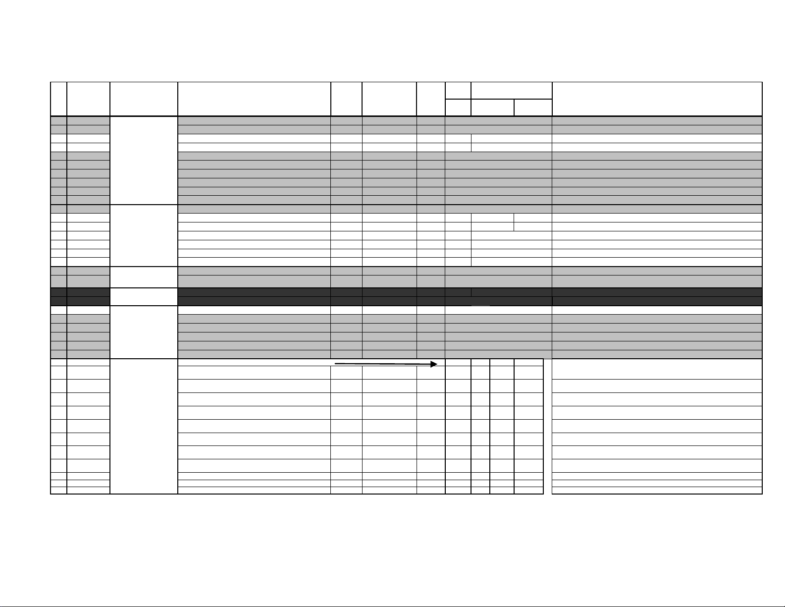
ADJUSTMENT ITEMS (5 OF 6)
VIVID
KV-32FV27 / 36FS13 / 36FS17 / 36FV27 / 38FS17
Register
Name
20
PUGA
21
4PUG
22
PYGA
23
4PYG
24
CHRO
25
SATA
26
YPKG
27
4YPK
28
YCOR
29
CLPL
0
RTCO
1
T2CO
2
V2CO
3
4COL
4
T2HU
5
V2HU
6
4SHU
0
XJGL
1
LNJ1
0
DUM1
1
VOSD
0
DISP
1
RAMW
2
ICMP
3
IPOR
4
FAWD
5
TILT
0 VPIC
1 VBRT
2 VCOL
3 VSHP
4 VVM
5 VTRI
6 VGMA
7 VBLK
8 VAPA Set Current Program Palette APACON 0,1 FIX by Palette
9 VSRT Set Current Program Pallette SRT 0,1 FIX by Palette
10 VNRM
PIP-YC
SDA9588X
DAC
CXA131
ID1
CXD2085
CCD
OP
M306V5
PALETTE
PROGRAM
5
Decoding Result Held For VCR Scanning
OSD Non-interlace Even/Odd Display
Set Current Program Pallette
PICTURE Reset Level
Set Current Program Pallette
BRIGHTNESS Reset Level
Set Current Program Pallette
COLOR Reset Level
Set Current Program Pallette
SHARPNESS Reset Level
Set Current Program Pallette
VM Reset Level
Set Current Program Pallette
Color Temp Reset Setting
Set Current Program Pallette
YC/J GAMMA
Set Current Program Pallette
Black Stretch
Set Current Program Pallette NRMD 0,1
Description Data Adj/Fix Initial 32" 36"/38" Comments
Range Data FV FS FV
Peak Level U Output
Peak Level U Output YUV Input
Peak Level Y Output
Peak Level Y Output YUV Input
UV Output Polarity
Color Saturation Adjustment
Y Peaking Adjustment
Y Peaking Adjustment YUV Input
Y Coring Enable
Clamp Pulse Length
Rotation Coil
Sub Color TV Input
Sub Color Video Input
Sub Color YUV Input
Sub Hue TV Input
Sub Hue Video Input
Sub Hue YUV Input
ID-1 Signal Location
CCD Dummy Register
VChip OSD Test Register
OSD Position
OSD RAM Window
OSD Non-interlace Threshold
Factory AutoWide Mode
Tilt Correction Spec
PROGRAM FOR EACH PALETTE MODE
0-255
0-255
0-255
0-255
0,1
0-15
0-7
0-7
0,1
0-3
0-63
0-7
0-7
0-7
0-7
0-7
0-7 Adj
0,1
0,1
0,1
0-63
0,1
0-15
0-3
0,1
0,1
0-63 FIX by Palette
0-63 FIX by Palette
0-63 FIX by Palette
0-63 FIX by Palette
0-3 FIX by Palette
0-3 FIX by Palette
0-3 FIX by Palette
0,1 FIX by Palette
FIX 52 52
FIX 36 36
Fix by Model 104 25 35
Fix by Model 129 27 37
FIX 0 0
FIX 8 9
FIX 7 7
FIX 7 7
FIX 1 1
FIX 0 0
FIX 31 31
Adj 120 120 111 106
Adj 120 120 122
Adj 120 120 117
Adj 15 15 16
Adj 15 15 18
FIX 0 0
FIX 0 0
FIX 0 0
Adj 15 15
FIX 0 0
FIX 4 4
Fix 1 1
Fix 0 0
Fix 0 2
FIX by Palette
114
15 15 16
STD MOVIE SPORTS
50 63 50 38 63
31 31 31 31 31
31 38 31 31 38
31 31 31 31 31
1210 2
1012 0
2322 2
1111 1
1011 1
0 100 0
0000 1
0: 0.3Vpp, 192: 1.0Vpp, 255: 1.2Vpp
0: 0.3Vpp, 192: 1.0Vpp, 255: 1.2Vpp
0: 0.3Vpp, 192: 1.0Vpp, 255: 1.2Vpp
0: 0.3Vpp, 192: 1.0Vpp, 255: 1.2Vpp
0: +U/+V output, 1: -U/-V output
0: No color, 8: nominal saturation, 15: nominal x 1.875
0: No peaking, 7: Strongest Peaking
0: No peaking, 7: Strongest Peaking
0: OFF, 1: ON
0=5ms, 1=3.75ms, 2=2.5ms, 3=1.25ms
Rotation coil adjustment for nominal value
TV Sub Color Adjustment (CXA2039 YUV Models AT DAC)
VIDEO1-3 Sub Color Adjustment (CXA2039 YUV Models at DAC)
YUV Sub Color Adjustment (CXA2039 YUV Models at DAC)
TV Sub HUE Adjustment (CXA2039 YUV Models at DAC)
VIDEO1-3 Sub HUE Adjustment (CXA2039 YUV Models at DAC)
YUV Sub HUE Adjustment (CXA2039 YUV Models at DAC)
Hold data during VCR variable speed playback
Search for ID-1 data +/- one line in VBI
Used to display CC data in Service Mode
Used to display VChip data in Service Mode
OSD horizontal position
0: 0 fields, 15: 15 fields
0=Even OSD display, 1= Odd OSD display, 2&3=N/A
0= No Autowide in RF mode, 1= Autowide in RF Mode
0= New Tilt Spec for AA2U (less VANG offset), 1= AA2W/AA2H Tilt Spec
0=MIN, 63=MAX
0=MIN, 63=MAX
0=MIN, 63=MAX
0=MIN, 63=MAX
0=OFF, 1=LOW, 2=HIGH, 3=N/A
0=COOL, 1=NEUTRAL, 2=WARM, 3=N/A
0=GAMMA CORRECTION OFF, 3=+12 IRE CORRECTION @ 40 IRE INPUT
0=BLACK STRETCH OFF, 1=BLACK STRETCH ON
0=APACON OFF, 1=APACON ON
0=SRT OFF, 1=SRT ON
0=3D YCS, 1=2D YCS
— 20 —
ADJUSTMENT ITEMS (6 OF 6)
)
)
)
KV-32FV27 / 36FS13 / 36FS17 / 36FV27 / 38FS17
Register
Name
0 RDOF Red Drive offset for WARM 0-63 FIX
1 GDOF Green Drive offset for WARM 0-63 FIX
2 BDOF Blue Drive offset for WARM 0-63 FIX
3 RCOF Red Cutoff offset for WARM 0-31 FIX
4 GCOF Green Cutoff offset for WARM 0-31 FIX
5 BCOF Blue Cutoff offset for WARM 0-31 FIX
6 DCOF
0 ID-0 ID-0 (Language/Color Systems) 0-255 Fix by model 89 See ID map
1 ID-1 ID-1 (Input/Output Conifguration) 0-255 Fix by model 6 3 See ID map
2 ID-2 ID-2 (Audio) 0-255 Fix by model 239 See ID map
3 ID-3 ID-3 (OSD/Timer/V-chip/Ch Fix) 0-255 Fix by model 99 See ID map
4 ID-4 ID-4 (CC/Spot Killer/etc) 0-255 Fix by model 139 See ID map
5 ID-5 ID-5 (V-series Features/etc) 0-255 Fix by model 181 See ID map
6 ID-6 ID-6 (PiP/Ant Sw related) 0-255 Fix by model 6 See ID map
7 ID-7 ID-7 (Special Models/etc)
VALUE
VALUE
TEMP
WARM
COLOR
ID
MAP
OFFSET
Dynamic Color setting for WARM 0,1
= Not Used for AA-2U
= Fixed Item For AA-2U
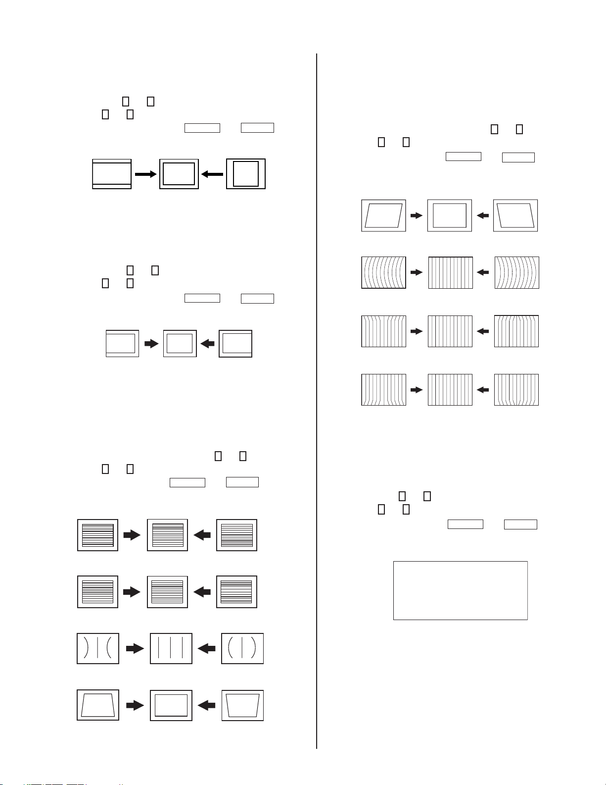
4-5. FEATURE ID MAP
ID
ID7
7
Description Data Adj/Fix Initial 32" 36"/38" Comments
Range Data FV FS FV
Red Drive MOVIE=RDRV(RDR4)-RDOF
Green Drive MOVIE=GDRV(GDR4)-GDOF
Blue Drive MOVIE=BDRV(BDR4)-BDOF
Red Cutoff MOVIE=RCUT(RCU4)-RCOF
GREEN Cutoff MOVIE=GCUT(GCU4-GCOF)
BLUE Cutoff MOVIE=BCUT(BCU4)-BCOF
0=OFF, 1=ON
See ID map
0-255
FIX
Fix by model 24
00
44
15 15
00
22
77
00
refer to NVM ID Chart
4-6. PROGRAM PALETTE SETTINGS
24
TV
SERVICE
00011000
Picture (VPIC) 63 50 38 63
Vivid Standard Movie Sports
Brightnness (VBRT) 31 31 31 31
Color (VCOL) 38 31 31 38
Sharpness (VSHP) 31 31 31 31
1
M306V5ME-1015P
VERSION: 1.0__
NVM:G
VM
C Temp
1
(VVM) 2102
(VTRI) 2102
Gamma (VGMA) 3222
Note: Check to be sure NVM is good (NVM: G)
0RGHO 'HVWLQDWLRQ ,' ,' ,' ,' ,' ,' ,' ,'
.9)9 86
.9)9 &1'
.9)6 86
.9)6 &1'
.9)6 +$:$,,
.9)6 86
.9)6 +$:$,,
.9)9 86
.9)9 &1'
.9)9 +$:$,,
.9)6 (
Blk Comp (VBLK) 1111
V Apa Comp (VAPA) 0111
SRT ON/OFF (VSRT) 1000
NRMD (VNRM) 0001
1
Setting of 3 is invalid for these registers
— 21 —
KV-32FV27 / 36FS13 / 36FS17 / 36FV27 / 38FS17
TO PROGRAM PROGRAM PALETTE RESET
LEVELS
1. Switch to Program Palette to edit.
2. Enter Service Mode.
3. Set desired values for current Program Palette settings.
4. Write into memory by pressing
5. Repeat steps 1-4 for each palette.
Example
To Set RESET Level of Standard Mode to 60%
1. Switch to STANDARD Palette.
2. Enter Service Mode.
3. Change value of VPIC to 38 (38/63 = 60%)
4. Write into memory by pressing
5. Enter Video Menu and press
6. Reset level of picture for STANDARD PALETTE ONLY is now 38
steps.
MUTING
MUTING
RESET
.
then
then
ENTER
ENTER
.
.
4-7. A BOARD ADJUSTMENTS
SUB CONTRAST ADJUSTMENT (RDRV,
RDR4)
1. Input a 75% color-bar signal.
2. Set to: VIDEO mode = Standard, COLOR = Minimum,
PICTURE = 100%, GON = 0 (OFF), BON = 0 (OFF)
3. Set to Service Adjustment Mode and connect an oscilloscope to
1
pin
of CN351 on the A Board.
1
4. Set RDRV with
5. Adjust with
1.95 ± 0.05 Vp-p (ALL EXCEPT KV-32FV27).
6. Write into memory by pressing
7. Repeat steps 1-6 for RDR4 using Video 4 input.
and 4 .
3
and 6 for: 1.85 ± 0.05 Vp-p (KV-32FV27 ONLY),
MUTING
then
ENTER
.
SUB HUE, SUB COLOR ADJUSTMENT
(T2HU, T2CO, V2HU, V2CO, 4SHU, 4COL)
Note: T2HU and T2CO are for Tuner inputs.
V2HU and V2CO are for all other Video inputs.
4SHU and 4COL are for Video 4 input.
1. Input a 75% color-bar signal.
2. Set to Service Adjustment Mode and set: VIDEO mode = Standard,
PICTURE = 100%, COLOR = 50%, HUE = 50%.
3. Connect an oscilloscope to Pin
4. Select T2HU and T2CO with
5. Adjust with
6. Write into memory by
7. Repeat steps 1-6 for V2HU & V2C0 and 4SHU & 4COL.
3
and 6 for a fl at ± 50mV.
MUTING
V1
3
of CN351 on the A Board.
1
and 4 .
then
V2 V3
ENTER
.
V4
V. SIZE ADJUSTMENT (VSIZ)
1. Input a cross-hatch signal.
2. Set to Service Adjustment Mode.
3. Select VSIZ with
4. Adjust with
5. Write into the memory by pressing
1
and 4.
3
and 6 for the best vertical size.
MUTING
then
ENTER
.
White
1.95 ± 0.05 Vp-p (ALL EXCEPT KV-32FV27)
1.85 ± 0.05 Vp-p (KV-32FV27 ONLY)
Black
SUB BRIGHT ADJUSTMENT (SBRT)
1. Set to Service Adjustment Mode.
2. Input a gray scale pattern signal.
3. Set the PICTURE to minimum, and BRIGHT to normal.
white
1
and 4 .
3
and 5 so that the stripe second
then
MUTING
second from the right
black
ENTER
4. Select SBRT with
5. Adjust SUB BRIGHT level with
from the right is faintly visible.
6. Write into the memory by pressing
.
V. POSITION ADJUSTMENT (VPOS)
1. Input a cross-hatch signal.
2. Set to Service Adjustment Mode.
3. Select VPOS with
4. Adjust with
5. Write into the memory by pressing
— 22 —
1
and 4 .
3
and 6 for the best vertical center.
MUTING
then
ENTER
.
KV-32FV27 / 36FS13 / 36FS17 / 36FV27 / 38FS17
H. SIZE ADJUSTMENT (HSIZ)
1. Input a monoscope signal.
2. Set to Service Adjustment Mode.
3. Select HSIZ with
4. Adjust with
5. Write into the memory by pressing
1
and 4 .
3
and 6 for the best vertical size.
MUTING
then
H. POSITION ADJUSTMENT (HPOS)
HPOS Range is from 0~15.
1. Input a monoscope signal.
2. Set the Service Adjustment Mode.
3. Select HPOS with
4. Adjust with
5. Write into the memory by pressing
1
and 4 .
3
and 6 for the best horizontal center.
MUTING
then
ENTER
ENTER
V ANGLE (VANG), V BOW (VBOW), UPPER
PIN (UPIN) AND LOW PIN (LPIN)
ADJUSTMENTS
1. Input a monoscope signal.
2. Set to Service Adjustment Mode.
.
3. Select VANG, VBOW, UPIN, and LPIN with
4. Adjust with
5. Write the memory by pressing
3
and 6 for the best picture.
MUTING
V ANGLE (VANG)
V BOW (VBOW)
.
UPPER PIN (UPIN)
1
then
and 4 .
ENTER
.
V LINEARITY (VLIN), V CORRECTION (VSCO),
PIN AMP (PAMP) AND PIN PHASE (PPHA)
ADJUSTMENTS
1. Input a cross-hatch signal.
2. Set to Service Adjustment Mode.
3. Select VLIN, VSCO, PAMP, and PPHA with
4. Adjust with
5. Write the memory by pressing
3
and 6 for the best picture.
V LINEARITY(VLIN)
VS CORRECTION (VSCO)
PIN AMP (PAMP)
MUTING
1
then
and 4 .
ENTER
.
LOW PIN (LPIN)
OSD POSITION ADJUSTMENT (DISP)
1. Input a color-bar signal.
2. Set to Service Adjustment Mode.
3. Select DISP with
4. Adjust with
5. Write the memory by pressing
1
and 4.
3
and 6 for adjustment of characters to center.
then
MUTING
OP 0 16 Service
DISP TV
ENTER
.
PIN PHASE (PPHA)
— 23 —
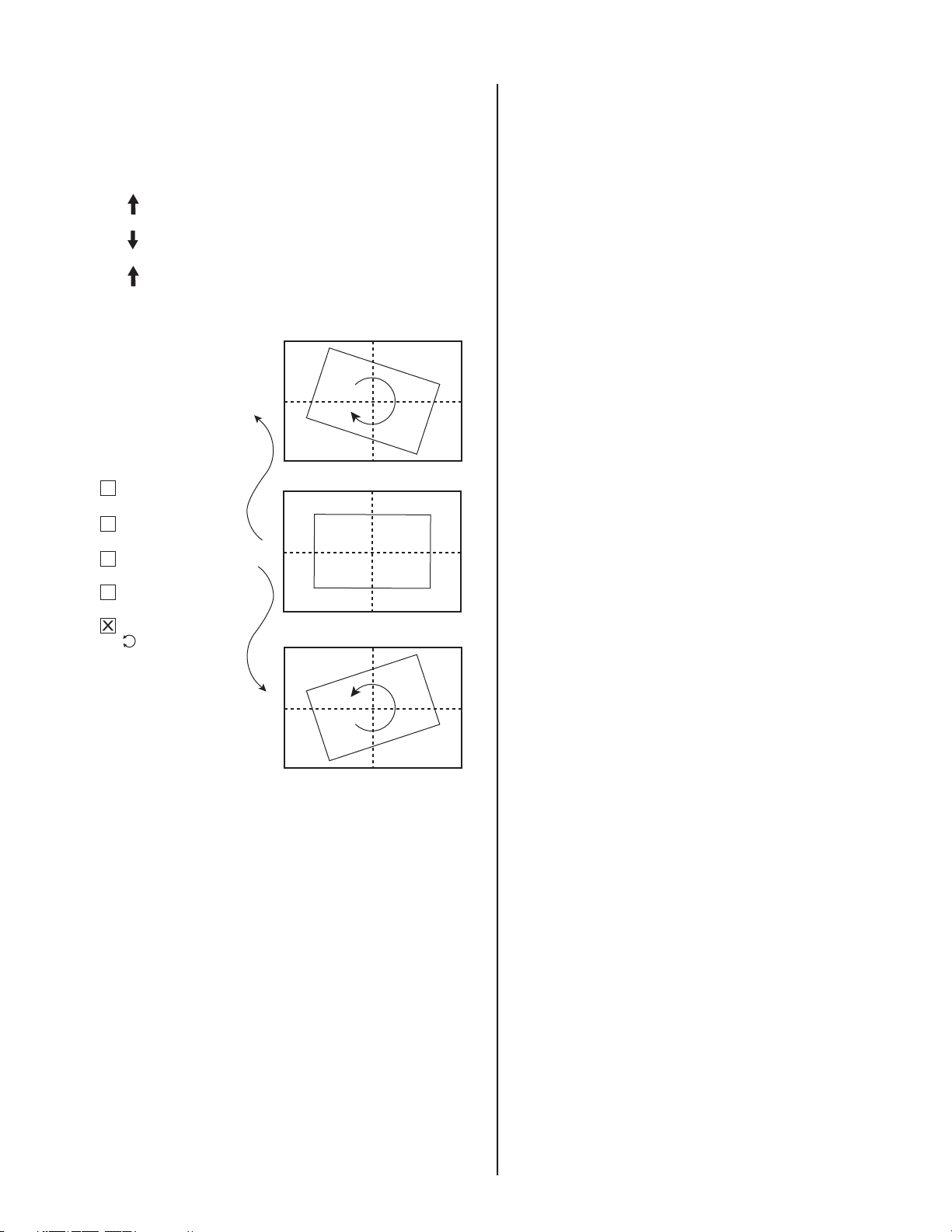
ROTATION COIL ADJUSTMENT
1. Input a monoscope signal.
2. Push the Menu button on the Remote.
3. Select the “Set-up” mode.
4. Select “Tilt Correction”. Confi rm that number (0) color changes to red.
5. Push
6. Push
7. Push
(+) on the Remote. Confi rm that the number increases up to
+5 and the picture rotates clockwise.
(-) on the Remote. Confi rm that the number decreases down
to -5 and the picture rotates counter-clockwise.
(+) on the Remote. Return the value to 0.
SET-UP
+5
Channel Set-up
KV-32FV27 / 36FS13 / 36FS17 / 36FV27 / 38FS17
Favorite Channel
Video Label
Language: English
Tilt Correction:
Menu
0
-5
— 24 —
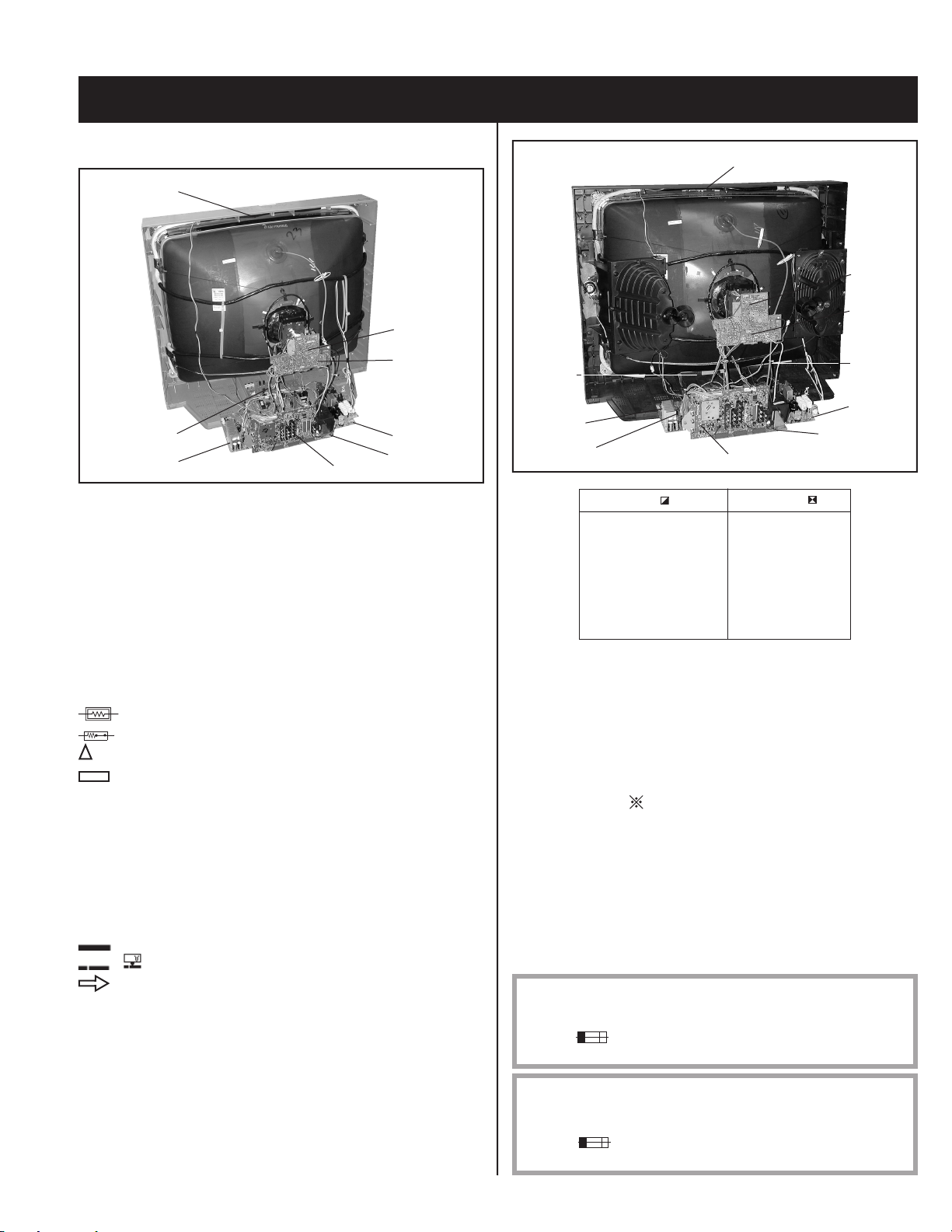
SECTION 5: DIAGRAMS
KV-32FV27 / 36FS13 / 36FS17 / 36FV27 / 38FS17
5-1. CIRCUIT BOARDS LOCATION
HX Board
HS Board
AK Board
KV-36FS13/36FS17/38FS17 ONLY
C Board
WA Board
G Board
A Board
UY Board
5-2. PRINTED WIRING BOARDS AND
SCHEMATIC DIAGRAMS INFORMATION
All capacitors are in µF unless otherwise noted. pF : µµF 50WV or less
are not indicated except for electrolytics and tantalums.
All electrolytics are in 50V unless otherwise specifi ed.
All resistors are in ohms. K=1000, M=1000k
Indication of resistance, which does not have one for rating electrical
power, is as follows:
Pitch : 5mm
Rating electrical power : 1/
1
/
W in resistance, 1/
4
: nonfl ammable resistor.
: fusible resistor.
: internal component.
: panel designation and adjustment for repair.
All variable and adjustable resistors have characteristic curve B, unless
otherwise noted.
Readings are taken with a color-bar signal input.
Readings are taken with a 10M digital multimeter.
Voltages are DC with respect to ground unless otherwise noted.
Voltage variations may be noted due to normal production tolerances.
All voltages are in V.
S : Measurement impossibillity.
: B+line.
: B-line. (Actual measured value may be different).
: signal path. (RF)
Circled numbers are waveform references.
The components identifi ed by X in this basic schematic diagram have
been carefully factory-selected for each set in order to satisfy regulations
regarding X-ray radiation. Should replacement be necessary, replace
only with the value originally used.
When replacing components identifi ed by Y, make the necessary
adjustments as indicated. If the results do not meet the specifi ed value,
change the component identifi ed by X and repeat the adjustment until
the specifi ed value is achieved. (Refer to Safety Related Adjustments
on Page 14.)
When replacing the parts listed in the table below, it is important to
perform the related adjustments.
W and 1/
10
W
4
W in chip resistance.
8
— 25 —
KV-32FV27/36FV27 ONLY
HX Board
C Board
WA Board
HB Board
HA Board
G Board
AK Board
A Board
T Board
Part Replaced ( )
R387, R550, R529, R530,
R531, R532, R533, D519,
D520, D521, IC501, C531,
C532, T503, IC351, Q301,
R356, R359, R361,
D302.....................A Board
IC643, R661.........G Board
UX Board
Adjustment ( )
HV HOLD-DOWN
R530,R531
REFERENCE INFORMATION
RESISTOR : RN METAL FILM
: RC SOLID
: FPRD NONFLAMMABLE CARBON
: FUSE NONFLAMMABLE FUSIBLE
: RW NONFLAMMABLE WIREWOUND
: RS NONFLAMMABLE METAL OXIDE
: RB NONFLAMMABLE CEMENT
: ADJUSTMENT RESISTOR
COIL : LF-8L MICRO INDUCTOR
CAPACITOR : TA TANTALUM
: PS STYROL
: PP POLYPROPYLENE
: PT MYLAR
: MPS METALIZED POLYESTER
: MPP METALIZED POLYPROPYLENE
: ALB BIPOLAR
: ALT HIGH TEMPERATURE
: ALR HIGH RIPPLE
The components identifi ed by shading and ! symbol are critical for safety. Replace
only with part number specifi ed.
The symbol indicates a fast operating fuse and is displayed on the component
side of the board. Replace only with fuse of the same rating as marked.
Les composants identifi es par un trame et une marque
securite. Ne les remplacer que par une piece portant le numero specifi e.
Le symbole indique une fusible a action rapide. Doit etre remplace par une
fusible de meme yaleur, comme maque.
!
sont critiques pour la
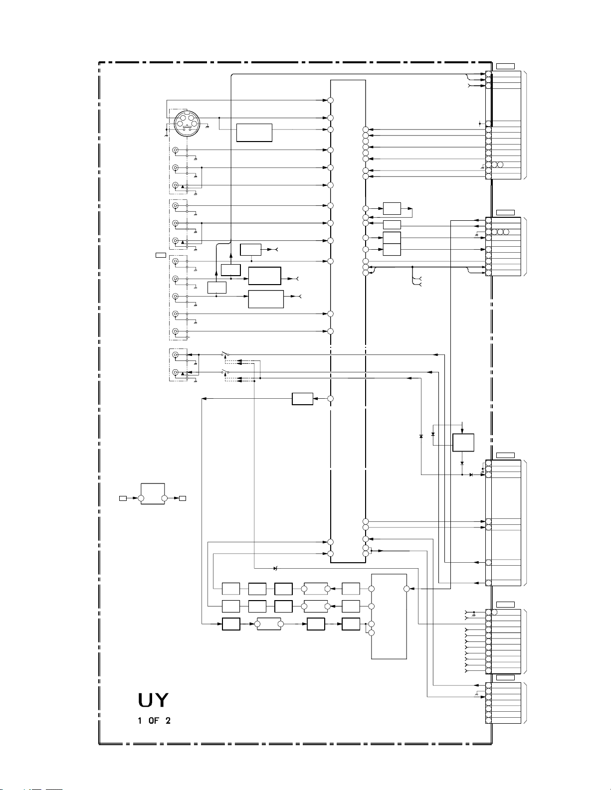
5-3. DIAGRAMS
BLOCK DIAGRAM (1 OF 6) (KV-36FS13 / 36FS17/ 38FS17 ONLY)
AV SWITCH
IC261
5
C1
3
Y1
6
1
2
4
7
8
10
15
14
19
V4
SSW1
20
L4
21
Y4
22
R6
V1
23
C4
24
SSW4
L1
64
TV R
62
TV L
R1
V2
Y OUT1
TV V
L2
C OUT1
R2
V OUT3Y5V OUT3
Y3
GAIN
SCL
SDA
BUFF
56
Q212
27
63
BUFF
Q265
BUFF
58
Q262
BUFF
35
Q264
48
31
32
L3
S TERMINAL BLOCK 3P
VIDEO1
PIN JACK BLOCK 3P
VIDEO3
VIDEO4
J231
YC
34
12
BUFFERS
Q1201,1202
Q1205,1207
V
L
R
J232
V
L
R
BUFF
J236
DVD
Y
B-Y
R-Y
BUFF
Q211
Q207
BUFF
Q210
BUFFERS
Q202,Q205
BUFFERS
Q203,Q206
DVD-Y
Q208
Q209
DVD B-Y
DVD R-Y
L
KV-32FV27 / 36FS13 / 36FS17 / 36FV27/ 38FS17
CN262
10
DVD R-Y
11
DVD B-Y
DVD Y
SCL
SDA
8
12
3
5
1
6
4
7
2 9
15
14
15
1
2
3
5
8
9
12
13
FRONT-V
FRONT-L
FRONT-Y
FRONT-R
FRONT-C
FRONT-S.SW
CN264
6
MAIN-C
MAIN-Y
O.MUTE
DVD ATTN
SCL
SDA
DVD Y
TO
A BOARD
9V
13
TV-R
TV-L
FSC
TV-V
10
CN270
E
14
E
TO
A BOARD
CN271
PIN JACK BLOCK 2P
VAR. OR
FIX OUT
9V
5V REG
IC2006
I O
R
J233
L
R
5V
(3D LINE COMB FILTER)
(AV SW)
16
R3
Q235
MUTE
Q236
MUTE
BUFF
Q263
53
V OUT1
9V
Q1051
OFF
MUTE
54
R OUT1
52
L OUT1
60
V6
49
Y IN1
59
L6
51
61
R6
C IN1
D248
AMP
BUFF
Q2009
Q2007
Q2006
BUFF
AMP
Q2010
Q2008
Q2005
BUFF
Q2019
FL2004
12
FL2001
BUFF
12
FL2002
BUFF
12
6
BUFF
Q2018
BUFF
6
Q2003
BUFF
6
Q2004
BUFF
Q2014
ACO
AYO
CLPO
ADIN
DIG COMB
FILTER
IC3504
37
FIN
E
9V
P B-Y
P R-Y
PY
P YS
2CH BLK
MAIN VP
MAIN HP
DVD SW2
7
9
1
2
3
7
10
9
8
5
6
6712
4
5
8
9
10
11
2
3
1
1
2
3
4
5
6
7
CN265
OFF MUTE
CN263
2 CH BLCK
MAIN VP
MAIN HP
DVD SW2
CN261
E
E
R
L
A BOARD
CN1462
TO
VAR L
VAR R
E
9V
AMUTE
P B-Y
P R-Y
PY
TO AK
PYS
BOARD
CN272
2-DET
E
2-L/R
M-IN1
M-IN3
M-IN4
M-OUT
CN1467
TO AK
BOARD
— 26 —
AA2U-901-FS-BD
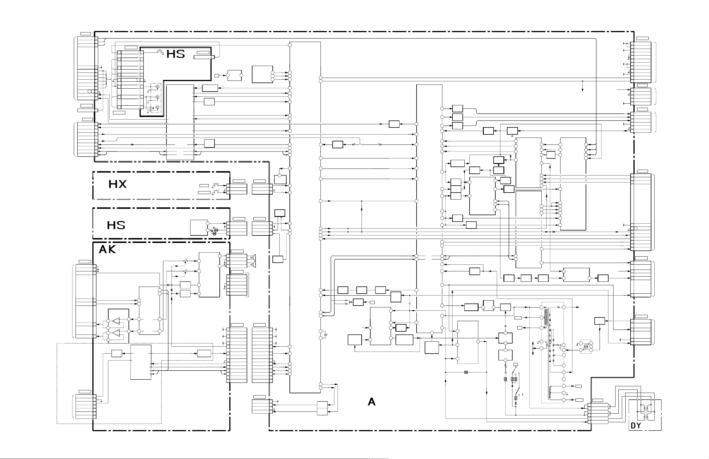
BLOCK DIAGRAM (2 OF 6) (KV-36FS13 / 36FS17 / 38FS17 ONLY)
CN270
10
DVD R-Y
11
DVD B-Y
8
TO UY
BOARD
CN265
TO UY
BOARD
CN262
TO UY
BOARD
CN261
TO UY
BOARD
CN264
FRONT-V
FRONT-L
FRONT-Y
FRONT-R
FRONT-C
FRONT-S.SW
CN1233
FRONT-R
O.MUTE
CH-BLK
SCL
SDA
CN1464
OFF MUTE
CN1467
2-DET
2-L/R
M-IN1
M-IN3
M-IN4
M-OUT
DVD Y
9V
12
9V
3
5
1
6
4
7
29
13
E
15
TV-R
14
TV-L
1
CN271
15
FSC
TV-V
1
3
MAIN-C
5
MAIN-Y
8
7
12
13
3
E
7
E
10
9
R
8
L
1
5
VAR L
VAR R
E
2
7
6
6
1
2
3
4
5
6
7
CN1231
VAR-AMP
IC1402
BUFF
Q106
CN1232
7
MENU KEY
FRONT C
5
8
FRONT Y
4
FRONT-SW
1
E
6
FRONT V
3
FRONT L
2
FRONT R
(AUDIO AMP)
(AUDIO CNTL)
(2ND TUNER)
3
5
(KV-36FS17 ONLY)
(KEY)
(IR DETECTOR)
5
28
AUDIO PROC
21
12 12
SUB TUNER
TU101
DET OUT
DE-EM
MUTE OUT
AFT OUT
7
5
4
19
6
3
2
S2007-S2008
8
(FRONT A/V)
(MENU KEY)
J1231
V
L
R
R OUT
L OUT
DET OUT2
SUB TUNER
TU102
AFT OUT
FM MONO
DET OUT
SAP IND
ST IND
RF AGC
MODE
MUTE
SCL
SDA
Q1464
Q1463
MUTE
18 5
SDA
17
SCL
IN R
IN L
Q1462
MUTE
Q1461
IC1401
21
L OUT
R OUT
SCL
SDA
DETECTOR
IC2001
CN1233
FRONT-R
11
SYNC SEP
POWER
FNC SWS
4
2
6
AGC MUTE
R IN
L IN
AUDIO AMP
IC1461
MUTE
Q105
Q1103
H-SEP
Q001
BUFF
Q005
S2001-S2005
1
2
R OUT
L OUT
1
S2006
STBY 5V
9V
7
12
9V
30V
5V REG
I O
Q1102
CN2002 CN1002
1
POWER ON
2
3
CN2001
1
SIRCS
2
STDBY 5V
4
ST LED
5
TIMER LED
CN1462
1
R
2
E
3
E
4
L
CN1463
1
AUDIO +B
2
AUDIO +B
3
AUDIO-E
4
AUDIO-E
NC
6
NC
CN1466 CN1101
6
STBY 5V
7
12
30V
3
SP MUTE
9
2H.SYNC 2H.SYNC
8
11
2-MUTE 2-MUTE
10
2-AFT
4
S CLK
5
S DATA
2
SIRCS
1
M-BUS POW
ANTENNA
SWITCH
MEMORY
IC002
POWER ON
E
KEY
CN1001
STDBY 5V
ST LED
TIMER LED
E
KEY
RM-CN
SP. BOX (R)
SP. BOX (L)
TO
G BOARD
CN642
STBY 5V
9V 9V
30V
SP MUTE
EE
2-AFT
S CLK
S DAT
SIRCS
M-BUS POW
CN1102
TO
ANTSW1
ANTSW2
9V
E
41
7 23
WP NVMWTN
6
SCL
SDA
1
2
3
1
2
4
5
6
7
12
3
9
8
11
10
4
5
2
1
4
3
2
1
25
5
26
51
40
35
44
46
36
37
50
52
24
25
12
4
RESET
1C003
45
42
SW
Q009
10
59
60
SW
Q008
STBY 5V
9V
30V
64
43
49
39
24
27
I-MENU
TUNING-MICON
IO-BLCKN
IO-BDAT
O-AGCMT
I-AFT
O-MONO
I-HSYNC
I-STEREO
O-SAP
I-SAPIND
O-MUTE
O-CHBLK
IO-SCLKN
IO-SDAT
I-RESET
I-POWERN
I-KEYN
I-SIRCS
O-TIMLED
O-STLED
O-SPKMT
I-2HSYNC
O-2MUTE
I-2AFT
IO-SCLKN
IO-SDAT
IC001
O-RELAY
IO-SCLKN
IO-SDAT
O-2ANTAU
O-ANTAUX
I-CVIN
O-CHBLK
O-AMUTE
O-DGC
O-XTAL
I-XTAL
KV-32FV27 / 36FS13 / 36FS17 / 36FV27 / 38FS17
CN1641
1
+B
12V
9V
H.DY(+)
H.DY(+)H.DY(+)
H.DY(-)
H.DY(-)
V.DY(-)
V.DY(+)
STBY 5V
FROM FBT
PIN 5
200V
9V
9V
FROM
CN1641
PIN 12
DGC
BUFF
Q352
BUFF
Q507
-15V
62
61
Y/C JUNGLE
IC355
BUFF
22
R OUT
G OUT
BUFF
Q307
BUFF
5
Q002
FSC/XTAL3
46
B OUT
IKIN
7
COMB
EB-YIN
9
COMB Y
ER-YIN
EYIN
28
O-R
29
O-G
30
O-B
28
R IN
27
G IN
SCP
26
B IN
HP/PRM
YOUT
20
O-YS
25
YS1
YUVSW
R-YOUT
21
O-YM
52
63
19
P-INT
B-YOUT
VTIM
HP/PRM
34
SCL
35
SDA
ABL IN
AFCFIL
SW
1
I-VP
2
I-HP
24
27
13
15
57
58
BUFF
Q103
BUFF
Q104
Q006
X001
12MHz
20PP
BUFF
Q007
SW Q003
Q016
FROM FBT
PIN 5
PROT
Q503,
Q504
9V
2
V CONTROL
IN2-
IC501
BUFF
Q004
HOLD
(MICON)
(Y/C/J)
(TUNER)
(PIN-MOD)
(V.DEF)
(H.DEF)
INV
BUFF
IN1+
5
6
IN1-
OUT2IN2+
OUT1
SW
13
Q301
PIN
PIN
7
OUT
DRIVE
Q511,Q512
VDRIVE+
5
VTIM
HD OUT
HP/PRM
11
E/W DRIVE
-VD
VM
15
NECK
PROTECT
Q562,
Q561
Q304
BUFF
23
Q305
BUFF
24
Q306
21
39
38
37
BGP BUF
Q359
17
BUFF
Q1301
BUFF
18
Q1302
BUFF
32
Q351
36
BUFF
31
Q313
30
5
18
34
35
3
20
13
19
18
14
H DRIVE
V-OUT
IC561
7
DRIVE+
3
1
DRIVE-
BUFF
Q310
BUFF
Q1353
10
1
OSC
SCP
SHP
YOUT
IC353
Y
SCL
SDA
VM
BUFF
Q314
BUFF
Q303
:HDT
T501
3 6
Q501
5
OUT
SW
Q311
17
BYOUT
18
RYOUT
16
YOUT
BUFF
Q370
INV
Q1352
14
17
11
12
19
8
CLP
YUV SW
SW
Q1354
BUFF
Q361
D/A CONV
IC1001
IC354
MAIN YSW
PB-YIN
PR-YIN
6
B-YIN
7
R-YIN
BUFF
5
YIN
Q369
INSEL
4
2
3
1
PY-IN
25
YM
2
6
HUE
5
COLOR
DVD SW2
15
SCL
14
SDA
BUFF
AMP
Q364
Q362
H OUT
Q502
200V
B+
3
:PMT
T502
1
5
:HLT
T505
2
B+
S501
S502
NS CORR
7
SW
Q1303
FBT
T503
4
T503
NX-4600
2
TO
CN503
PIN 1
6
5
TO
IC501
PIN 3
TO CN1941
N/S MUTE
DVD B-Y
10
BYOUT
DVD R-Y
9
RYOUT
DVD Y
12
TVOUT CLAMP
YUV SW
IC352
19
TVIN
DLYSW
13
YUVSW
6
HUE
17
COLOR
16
22
R-YIN
21
B-YIN
2
SW
VM SW
IC351
1 7
HV1
TF TRANSFORMER
FV
13
SV
12
11
10
9
15V
8
7
-15V
PIN 4
V OUTV1
HIGH VOLTAGE
3
2
1
5
TO CRT
T504
34
2
1
6
CN501
1
2
3
4
5
6
+B
2
+B
8
12V
GND
4
5
GND
NC
3
6
9V
9V
7
9
GND
STBY 5V
10
11
PWRON
12
DGC
CN503
1
HEATER
2
E
3
NC
4
NC
5
200V
CN351
1
R
2
G
3
B
4
9V
5
E
6
IK
CN272
P B-Y
8
P R-Y
9
PY
4
9V
6712
E
10
PYS
5
AMUTE
11
2 CH BLCK
2
MAIN VP
3
MAIN HP
13
DVD SW2
CN1941
6
N/S CORR
4
N/S MUTE
1
VM OUT
5
H-PULSE
CN1942
4
DF H-DRIVE
2
V-DRIVE
3
-15V
1
V-PULSE
H.DY H.DY V.DY V.DY
BOARD
CN1764
BOARD
CN1761
FROM UX
BOARD
CN263
TO WA
BOARD
CN941
TO WA
BOARD
CN942
TO G
BOARD
CN641
TO C
TO C
— 27 —
AA2U-901-FS-BD
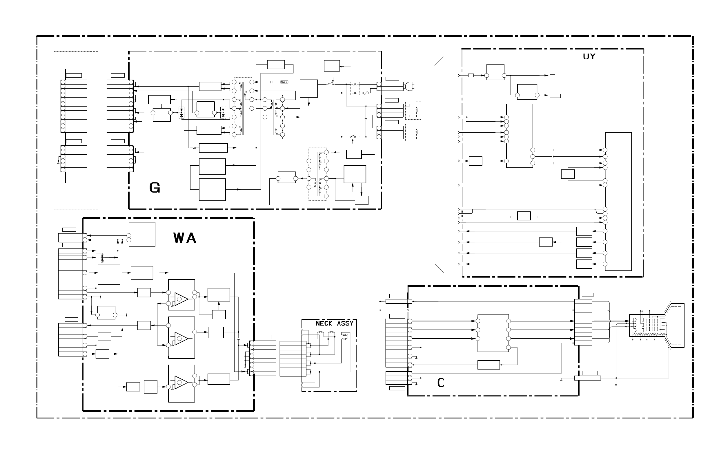
BLOCK DIAGRAM (3 OF 6) (KV-36FS13 / 36FS17 / 38FS17 ONLY)
KV-32FV27 / 36FS13 / 36FS17 / 36FV27 / 38FS17
A BOARD
CN1941
A BOARD
CN1942
(KV-36FS17 ONLY)
G21G2 5
G4
R
G
B
H2
(PIP)
28
26
24
1
2
10
6
5
3
4
16
17
18
15
PIP PROC
IC3303
CVBS1
Y/CVBS2
C/CVBS3
XIN
XQ
T2
SCL
SDA
SCP
VP
V OUT3
Y OUT2
U OUT1
SEL
H1
CHASSIS
1
H
H2
CV KR G1 G4
CRT
KG G2
KB
(FROM FBT)
HV
FROM A
BOARD
CN1641 CN641
1
+B
+B
2
12V
8
GND
4
5
GND
N.C.
3
9V
6
9V
7
GND
9
STBY 5V
10
11
PWRON
DGC
12
STBY 5V
PWRON
1
+B
2
+B
12V
8
4
GND
5
GND
N.C.
3
6
9V
9V
7
GND
9
10
11
12
DGC
CNTL
Q649,Q650
O
9V REG
IC641
I
+B RECT
12V REG
O
IC650
AUDIO RECT
D643
I
D641
CN1463 CN642
1
AUDIO +B
2
AUDIO +B
3
AUDIO -
4
AUDIO -
5
6
FROM AK
BOARD
CN981
N/S COIL +
N/S COIL -
AU +B
AU +B
AU - E
N.C.
N.C.
3
1
AU - E
1
2
3
4
5
NC
6
NC
(POWER)
(SUPPLY)
NS DRIVE
IC961
4
2
PWR CONTROL
IC643
POWER ON
SOFT START
Q645,Q647
Q648
LATCH,OCP
FOLD BACK
Q652,Q653
Q651,Q624
BACKUP
Q646
(VELOCITY MOD.)
(QUAD POLE ROT.)
CN941
N/S CORR
N/S MUTE
TO
H-PULSE
CN942
DF H-DRIVE
TO
V-DRIVE
V-PULSE
6
4
BUFFER
Q941,942
Q966,968
1
VM
8
+B
5
2
12V
Q944,945,
+B
12V
AMP
949
9V REG
IC965
I O
4
Q943
2
AMP
3
-15V
-15V
SW
1
Q1966
9V
BUFF
Q1963
VM DRIVES
1,2
Q946,Q947
H-SAW
HP
Q962
BUFF
Q961
BUFF
Q1964
Q1967
IC963
3 1
X
6
DF-COMP
7
IC962
X
6
V-PARA
DRIVE
X
5
QP-H-DRIVE
7
1
1
7
Q963
Q965
PROT
Q963
QP DR
Q1961
QP DR
Q969,Q967
T605
PIT
11
10
1
2
3
9
4
8
7
6
5
1
2
3
4
5
6
7
8
CN961
Q.P. Q.P. -
Q.P. +
Q.P. +
E
E
VM
VM
PROTECT
Q623
R607
AC RECT
T603
PRT
5V REG
O
1
2
3
4
5
IC622
8
7
6
D602
REG
IC601
11
10
I
9
8
TO
NECK ASSY
1
Q.P.-
2
Q.P.-
3
Q.P.+
4
Q.P.+
5
E
6
E
7
VM
8
VM
DRIVER
Q648
RY600
T621
SBT
1
2
3
4
5
6
QP QP VM
T601&T602
RY601
DRIVER
Q644
CONVERTER
Q621
FROM CN641
PWR ON
F601
CN641
RELAY
5V REG
IC3302
I O
9V
DVD SW2
DVD R-Y
DVD B-Y
DVD Y
SUB V
9V
3.3V REG
IC3310
I O
YUV-SW
IC3308
9
DVD SW
10
DVD SW
11
DVD SW
3
DV IN
13
DU IN
1
DY IN
15
Y OUT
14
BUFF
Q3301
U OUT
2
Y IN
V OUT
4
CN602
1
AC WHITE
2
AC
CN601
1
DGC
2
NC
DGC
3
CN601
1
DGC
2
NC
3
DGC
AC IN
DGC
DGC
FROM
DGC
UY BOARD
1 OF 2
TO
5V
3.3V
X3302
2 0F 2
2CH BLK
PROT
Q622
SDA
SCL
MAIN HP
MAIN VP
P B-Y
PY
P R-Y
P YS
TO FBT G2
CN1765
(FROM FBT)
TO FBT FOCUS FOCUS
CN1761
TO
VM
A BOARD
CN351
A BOARD
TO
CN503
CN1764
1
R
2
G
3
B
4
9V
E
IK
H
200V
E
9V
5
6
1
4
200V
2
(RGB DRIVE)
(CRT DRIVE)
3
2
1
R IN
G IN
B IN
CRT AMP
IC1701
IK-BUFF
Q1790
R OUT
G OUT
B OUT
IK
BUFF
Q3317
BUFF
Q3307
BUFF
Q3306
HOOK UP
Q3312
BUFF
Q3315
Q3316
BUFF
J1761
3
7
8
9
5
12
11
10
8
HEATER
CN1766
1E
IC964
— 28 —
AA2U-901-FS-BD
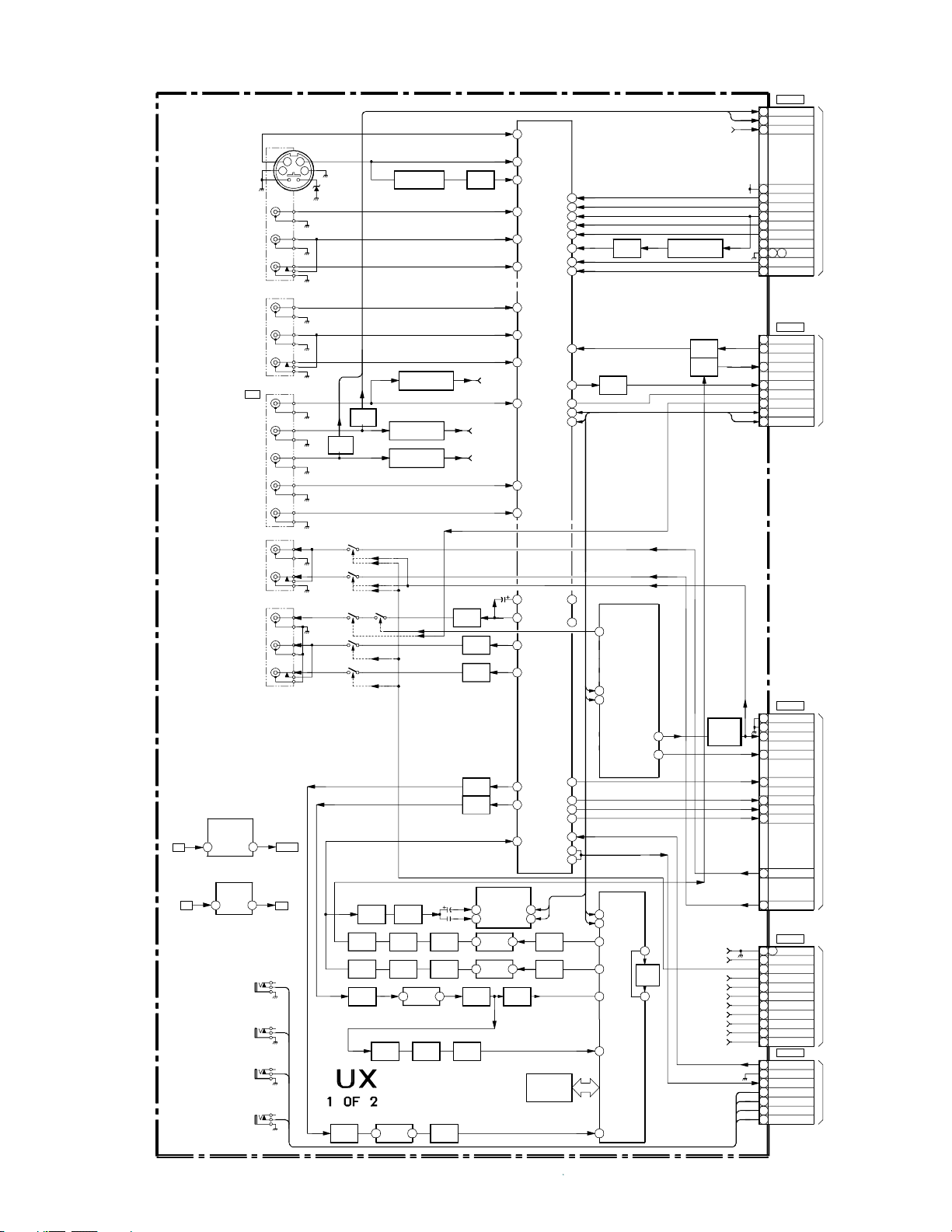
BLOCK DIAGRAM (4 OF 6) (KV-32FV27 / 36FV27 ONLY)
5
C1
AV SWITCH
IC261
3
Y1
6
SSW1
V4
L4
1
V1
Y4
R6
C4
2
L1
SSW4
TV R
4
R1
TV L
7
V2
8
L2
TV V
10
R2
DVD Y
V OUT3
15
Y3
SCL
SDA
14
L3
S TERMINAL BLOCK 3P
VIDEO1
PIN JACK BLOCK 3P
VIDEO4
VIDEO3
J231
YC
34
12
V
L
R
J232
V
L
R
J236
DVD
Y
B-Y
R-Y
L
BUFF
Q210
BUFF
Q211
Q1201,5,7
Q202,5,8
Q203,6,9
BUFF
Q201,4,7
BUFF
BUFF
SW
Q1202
BUFF
DVD B-Y
DVD R-Y
KV-32FV27 / 36FS13 / 36FS17 / 36FV27 / 38FS17
DVD Y DVD Y
19
20
21
22
23
24
64
62 14
63
35
48
31
32
BUFF
Q1203
BUFF
Q264
Q1204,8,6
BUFF
9V
BUFF
Q265
BUFF
Q262
10
11
12
15
15
12
13
8
3
5
1
6
4
7
2 9
1
3
5
8
7
CN262
DVD R-Y
DVD B-Y
FRONT-V
FRONT-L
FRONT-Y
FRONT-R
FRONT-C
FRONT-S.SW
13
CN264
MAIN-C
MAIN-Y
DVD ATTN
CH-BLK
9V
TV-R
TV-L
FSC
TV-V
SCL
SDA
CN270
E
TO
A BOARD
CN271
TO
A BOARD
PIN JACK BLOCK 2P
VAR. OR
FIX OUT
PIN JACK BLOCK 3P
MONITOR
5V
9V
SIRCS OUT
S-LINK IN1
SIRCS OUT
S-LINK IN3
JACK 3P
SIRCS OUT
S-LINK IN4
JACK 3P
SIRCS IN
S-LINK OUT
I
JACK 3P
JACK 3P
3.3V REG
IC2005
5V REG
IC2006
I O
16
VS IN
VP IN
FL2001
FL2002
IC2009
R3
Y IN1
49
V OUT1
53
52
54
58
56
27
Y5
SCL
SDA
23
23
BUFF
Q2014
C OUT1
Y OUT1
L OUT1
R OUT1
52
L OUT1
54
R OUT1
R OUT2
L OUT2
R OUT1
L OUT1
9
10
BUFF
Q2003
BUFF
Q2004
MEMORY
IC2003
3
Y MUTE
D/A
CONVERTER
IC1051
15
SCL
14
SDA
OFF
2CH BLK
MAIN UP
MAIN HP
DVD SW2
MUTE
Q1051
E
9V
P B-Y
P R-Y
PY
P YS
12
A1
1 4
IR
43
41
54
52
60
V6
59
L6
61
R6
59
SCL
60
SDA
ACO
83
FSC0
47
84
AYO
CLOCK
BUFF
Q2119
50
88
AYI
FSC1
CSI
76
3D COMB
IC2004
ACI
96
CN265
3
E
7
E
10
OFF MUTE
IR ON/OFF
2
IR R
1
IR L
9
R
8
L
5
VAR L
6
VAR R
CN263
6712
E
4
9V
5
AMUTE
P B-Y
8
P R-Y
9
PY
10
PYS
11
2 CH BLCK
2
MAIN VP
3
MAIN HP
1
DVD SW2
CN261
1
2-DET
2
E
3
2-L/R
4
M-IN1
5
M-IN3
6
M-IN4
7
M-OUT
TO AK
BOARD
CN272
A BOARD
CN1462
CN1467
TO
TO AK
BOARD
R
J233
L
R
J234
V
L
OUT
R
O
3.3V
Q235
MUTE
Q236
MUTE
Q233
MUTE
Q234
MUTE
Q231 Q246
MUTE MUTE
BUFF
Q237
BUFF
Q238
BUFF
Q239
BUFF
Q268
BUFF
Q263
ID1 DECODER
5V
J903
J904
J905
J902
BUFF
Q2016
Q2017
BUFF
BUFF AMP
Q2009
BUFF
Q2010
BUFF
Q2019
BUFF
Q2015
FL2003
2 3
Q2001
BUFF
Q2007 Q2006
AMP
Q2008
FL2004
BUFF
Q2013
(AV SW)
(3D LINE COMB FILTER)
6
7
BUFF
BUFF
Q2005
BUFF
32
Q2018
BUFF
Q2011
BUFF
Q2012
— 29 —
AA2U-901-FV-BD
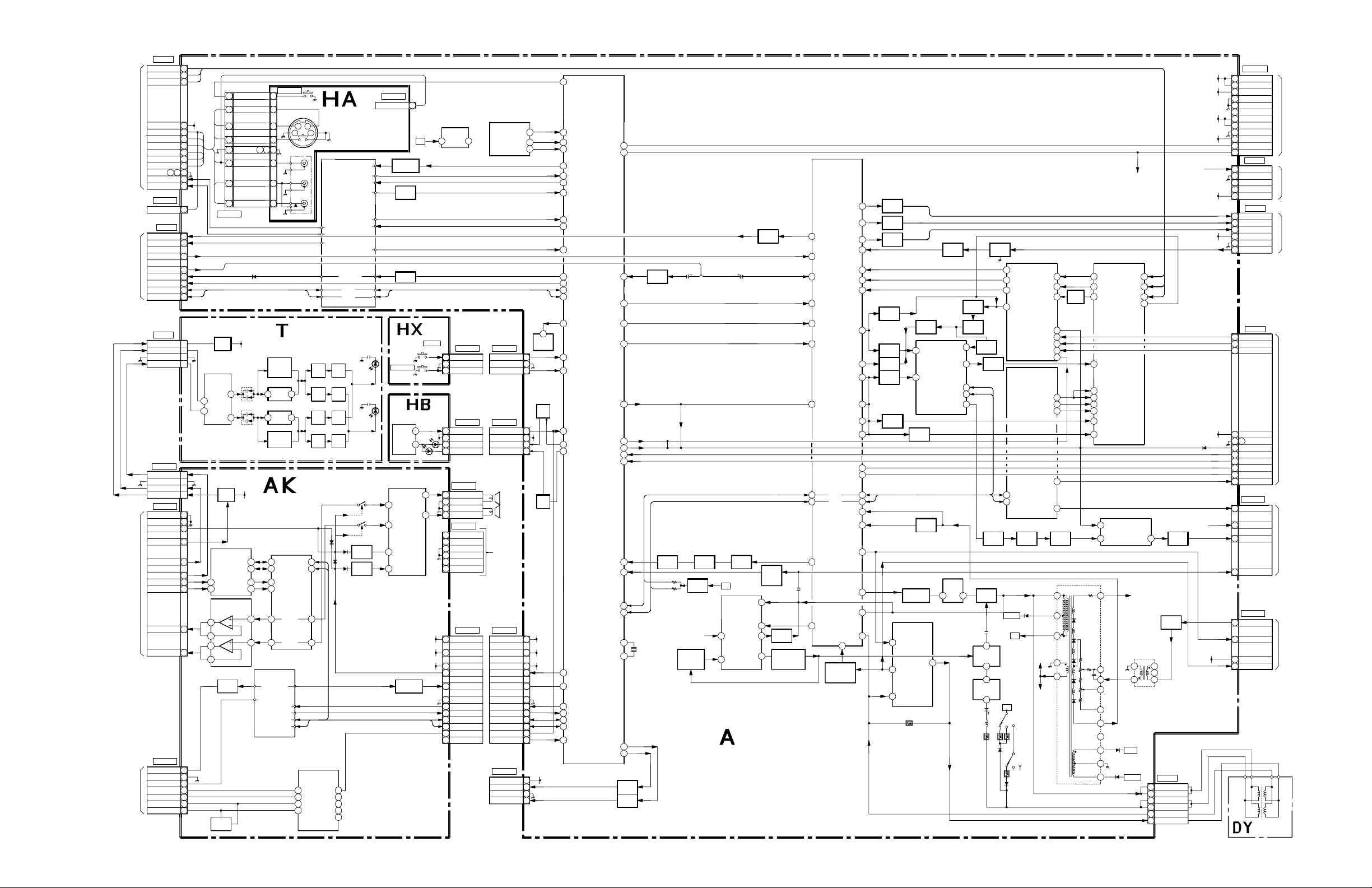
BLOCK DIAGRAM (5 OF 6) (KV-32FV27 / 36FV27 ONLY)
CN270
10
DVD R-Y
11
DVD B-Y
8
TO UX
BOARD
CN262
TO UX
BOARD
CN265
TO UX
BOARD
CN264
TO UX
BOARD
CN261
DVD Y
FRONT-V
FRONT-L
FRONT-Y
FRONT-R
FRONT-C
FRONT-S.SW
TV-R
TV-L
CN1233
FRONT-R
CN401
CN1465
CN1464
OFF MUTE
IR ON/OFF
CN1467
7
5
8
9V
12
9V
3
5
1
6
4
7
29
13
E
17
16
1
CN271
15
FSC
1
TV-V
3
MAIN-C
5
MAIN-Y
8
O.MUTE
7
CH-BLK
12
SCL
13
SDA
4
9V
3
R
2
E
L
1
IR L
1
E
2
IR R
3
9V
4
3
E
7
E
10
4
2
IR R
1
IR L
9
R
8
L
5
VAR L
6
VAR R
1
2-DET
2
E
3
2-L/R
4 11
M-IN1
5
M-IN3
6
M-IN4
7
M-OUT
4
1
6
3
2
CN1231
REG
Q403
???
IC401
7
L OUT
2
R IN
8
L IN
3
R OUT
SW
Q451
SRS
IC1403
R OUT
2 28
R IN
3
L IN
VAR-AMP
IC1402
1
2
7
6
BUFF
Q106
SW
Q1902
SDA
SCL
L OUT
MENU KEY
FRONT C
FRONT Y
FRONT-SW
FRONT V
FRONT L
FRONT R
D402
D403
E
9V
9V
5717
1
3
5
CN1232
7
5
8
4
17 9
6
3
2
L-CH
OSC
Q401
662
L 401
L 402
R-CH
OSC
Q402
18
SDA
SCL
5
IN R
28
IN L
AUDIO PROC
21
12 12
SUB TUNER
TU101
DET OUT
DE-EM
MUTE OUT
AFT OUT
SCL
SDA
S2007-S2010
J1231
(IR HEADPHONES)
2
IC1401
L OUT
R OUT
J1232
34
V
L
R
(AUDIO AMP)
(AUDIO CNTL/SRS)
(2ND TUNER)
(S-LINK)
SDA
SCL
SIRCS I/O
V1
V3
10
V4
9
TV
13
OUT
12
18
17
21
IC1902
BUFF
Q410
BUFF
Q404
BUFF
Q405
BUFF
Q411
STATUS
SIRCS
V1-S
V3-S
V4-S
(FRONT A/V)
(MENU KEY)
SUB TUNER
R OUT
L OUT
DET OUT2
DRVR
Q408
DRVR
Q406
DRVR
Q409
DRVR
Q407
CN1234
FRONT-R
AGC MUTE
Q1103
H-SEP
Q001
TU102
AFT OUT
FM MONO
DET OUT
ST IND
RF AGC
MODE
SAP IND
MUTE
SCL
SDA
IR EMIT
D408-411
BUFF
Q005
FNC SWS
S2001-S2005
IR EMIT
D404-407
DET
IC2001
Q1464
MUTE
Q1463
MUTE
Q1462
4
R IN
2
L IN
AUDIO AMP
MUTE
MUTE
Q1461
IC1461
6
11
MUTE
SYNC SEP
2
4
6
7
8
1
NVM
7 23
5V REG
I O
9V
Q1102
WP NVMWTN
IC002
6
SCL
5
SDA
(KEY)
POWER
CN2002 CN1002
S2006
1
POWER ON
2 2
E
3
KEY
(IR DET)
1
2 59
R OUT
L OUT
STBY 5V
CN2001
1
SIRCS
SIRCS
2 2
STDBY 5V
4
ST LED
5
TIMER LED
CN1462
7
1
R
2
E
3
E
12
4
L
CN1463
1
AUDIO +B
2
AUDIO +B
3
AUDIO-E
4
AUDIO-E
5
NC
6
NC
CN1466
6
7
9V
30V
9V 9V
12 12
30V 30V
SP MUTE SP MUTE
TIMER LED
SP. BOX (R)
SP. BOX (L)
G BOARD
Q105
EE
11 11
2-MUTE
10 10
2-AFT
4
S CLK
5 5
S DATA
SIRCS
1
M-BUS POW M-BUS POW
TO
ANTENNA
SWITCH
POWER ON
CN1001
STDBY 5V
CN642
CN1101
CN1102
KEY
RM-CN
ST LED
STBY 5VSTBY 5V
2H.SYNC2H.SYNC
2-MUTE
2-AFT
S CLK
S DAT
SIRCS
ANTSW1
ANTSW2
1
E
3
1
4
5
TO
6
7
33
99
88
4
22
1
4
9V
3
2
E
1
1C003
RESET
Q009
Q008
SW
SW
STBY 5V
9V
30V
KV-32FV27 / 36FS13 / 36FS17 / 36FV27/ 38FS17
CN1641
1
41
I-MENU
TUNING-MICON
IC001
12V
9V
H.DY(+)
H.DY(+)H.DY(+)
H.DY(-)
H.DY(-)
V.DY(-)
V.DY(+)
STBY 5V
FROM FBT
PIN 5
200V
9V
9V
FROM
CN1641
PIN 12
DGC
BUFF
Q352
BUFF
Q507
-15V
IO-BLCKN
25
IO-BDAT
26
51
O-AGCMT
40
I-AFT
35
O-MONO
44
I-HSYNC
46
I-STEREO
36
O-SAP
37
I-SAPIND
O-MUTE
50
52
O-CHBLK
24
IO-SCLKN
25
IO-SDAT
12
I-RESET
4
45
I-POWERN
42
I-KEYN
10
I-SIRCS
O-STLED
60
O-TIMLED
64
O-SPKMT
I-2HSYNC
43
O-2MUTE
49
39
I-2AFT
24
IO-SCLKN
27
IO-SDAT
34
I-MPOW
IO-SCLKN
IO-SDAT
O-2ANTAU
O-ANTAUX
O-RELAY
O-CHBLK
O-AMUTE
I-CVIN
O-XTAL
I-XTAL
62
61
O-DGC
Y/C JUNGLE
IC355
BUFF
22
R OUT
G OUT
BUFF
Q307
BUFF
5
Q002
46
7
9
FSC/XTAL3
COMB
COMB Y
B OUT
IKIN
EB-YIN
ER-YIN
EYIN
28
O-R
29
O-G
30
O-B
28
R IN
27
G IN
SCP
26
B IN
HP/PRM
YOUT
20
O-YS
25
YUVSW
YS1
R-YOUT
21
O-YM
52
63
19
P-INT
B-YOUT
VTIM
HP/PRM
34
SCL
35
SDA
ABL IN
AFCFIL
VDRIVE+
5
VTIM
HD OUT
HP/PRM
11
E/W DRIVE
-VD
VM
15
NECK
PROTECT
Q562, Q561
9V
V CONTROL
2
IN2-
HOLD
IC501
BUFF
Q004
IN1+
IN1-
OUT2IN2+
OUT1
(MICON)
(Y/C/J)
(TUNER)
(PIN-MOD)
(V.DEF)
(H.DEF)
INV
BUFF
Q003
5
6
SW
13
Q301
PIN
PIN
7
OUT
DRIVE
Q511,Q512
1
I-VP
2
I-HP
24
27
13
15
57
58
BUFF
Q103
BUFF
Q104
SW
Q006
X001
10MHz
20PP
FROM FBT
PIN 5
PROT
Q503,
Q504
BUFF
Q007
SW
Q016
Q304
BUFF
23
Q305
BUFF
24
Q306
21
39
38
37
BGP BUF
Q359
17
BUFF
Q1301
BUFF
18
Q1302
BUFF
32
Q351
36
BUFF
31
Q313
30
5
18
34
35
3
20
13
19
18
14
H DRIVE
Q501
V-OUT
IC561
7
DRIVE+
3
1
DRIVE-
BUFF
Q310
BUFF
Q1353
10
1
BUFF
Q314
OSC
SCP
YOUT
Y
SHP
SCL
IC353
SDA
VM
BUFF
Q303
:HDT
T501
3 6
5
OUT
BUFF
Q370
INV
Q1352
14
17
11
12
19
SW
Q311
SW
Q1354
BUFF
Q361
AMP
Q362 Q364
H OUT
Q502
3
:PMT
T502
1
5
:HLT
T505
2
S501
17
BYOUT
18
RYOUT
16
YOUT
8
CLP
YUV SW
D/A CONV
IC1001
IC354
MAIN YSW
PB-YIN
PR-YIN
6
B-YIN
7
R-YIN
BUFF
5
YIN
Q369
4
INSEL
2
3
PY-IN
1
YM
25
2
HUE
6
COLOR
5
DVD SW2
15
SCL
14
SDA
200V
B+
B+
S502
NS CORR
7
SWBUFF
Q1303
FBT
T503
4
T503
NX-4600
2
TO
CN503
PIN 1
6
5
TO
IC501
PIN 3
TO CN1941
N/S MUTE
10
DVD B-Y
BYOUT
9
DVD R-Y
RYOUT
12
TVOUT
DVD Y
CLAMP
YUV SW
IC352
19
TVIN
DLYSW
13
YUVSW
6
HUE
17
COLOR
16
22
R-YIN
21
B-YIN
2
SW
VM SW
IC351
1 7
HV1
TRANSFORMER
FV
13
SV
12
11
10
9
15V
8
7
-15V
PIN 4
V OUTV1
HIGH VOLTAGE
T504
6
TO CRT
3
2
1
5
TF
34
2
1
CN501
1
2
3
4
5
6
AA2U-901-FV-BD
+B+B
2
+B
8
12V
4
GND
5
GND
3
NC
6
9V
7
9V
9
GND
10
STBY 5V
11
PWRON
12
DGC
CN503
1
HEATER
2
E
3
NC
4
NC
5
200V
CN351
1
R
2
G
3
B
4
9V
5
E
6
IK
CN272
P B-Y
8
P R-Y
9
PY
4
9V
6712
E
10
PYS
5
A MUTE
11
2 CH BLCK
2
MAIN VP
3
MAIN HP
13
DVD SW2
CN1941
6
N/S CORR
4
N/S MUTE
1
VM OUT
5
H-PULSE
CN1942
4
DF H-DRIVE
2
V-DRIVE
3
-15V
1
V-PULSE
H.DY H.DY V.DY V.DY
BOARD
CN641
C BOARD
CN1764
C BOARD
CN1761
FROM UX
BOARD
CN263
TO WA
BOARD
CN941
WA BOARD
CN942
TO G
TO
TO
TO
— 30 —
 Loading...