SONY KV-32XBR400, KV-36XBR400, KV-38DRC1, KV-38DRC1C Service Manual Part4
KV-32XBR400/36XBR400/38DRC1/38DRC1C
3.7 WHITE BALANCE (CRT) AND SUB
BRIGHT ADJUSTMENT
White Balance
1. Input an all white 480I (15.734KHz) signal into the
VIDEO 1 input terminal to perform the white balance
(highlight, cut-off) adjustments. The parameters to adjust are
in the CXA2150P in service mode.
2. Set the following:
Picture: Full Mode
Pro Mode
Color: Center
3. Adjust white balance in the ser vice mode and set the
following data:
2150P-1
No. Name Control Function Avg. Data
05 RDRV R-DRIVE Fix: 41
06 GDRV G-DRIVE Adjust
07 BDRV B-DRIVE Adjust
08 RCUT R-CUT OFF Fix: 41
09 GCUT G-CUT OFF Adjust
10 BCUT B-CUT-OFF Adjust
3-8. RASTER CENTER ADJUSTMENT
1. Input a monoscope signal.
2. Set to NTSC (DRC) mode.
3. Enter service mode and set the following:
CXA2150P-2
No. Name Control Function Avg. Data
06 AGNG AGING1, AGING2 2
CXA2150D-2
No. Name Control Function Avg. Data
00 HBLK Blanking enable 0
02 HSIZ Horiz Size 31
4. Reduce HSIZ to see sides of raster.
5. Adjust H-Center with CXA2150D-2 00.
6. Adjust the best screen position with H-CENT and write data.
7. Restore aging, HSIZ and HBLK to original condition.
3-9. PICTURE DISTORTION ADJUSTMENTS
CXA2150D-1 and CXA2150D-2
4. Adjust sub-brightness: Input an all black signal (to IRE 7.5%
set up) 480i (15.75KHz) signal into the VIDEO 1 input
terminal and adjust the following parameter of the
CXA2150P-1.
CXA2150P-1
No. Name Control Function Avg. Data
04 SBRT SUB-BRIGHT Adjust
5. Check INITIAL DATA (Important)
2150P-1
No. Name Control Function Avg. Data
00 SBOT SUB-BRT OFFSET 7
12 SBOF SUB-BRT OFFSET 63
6. Repeat steps 3 to 5.
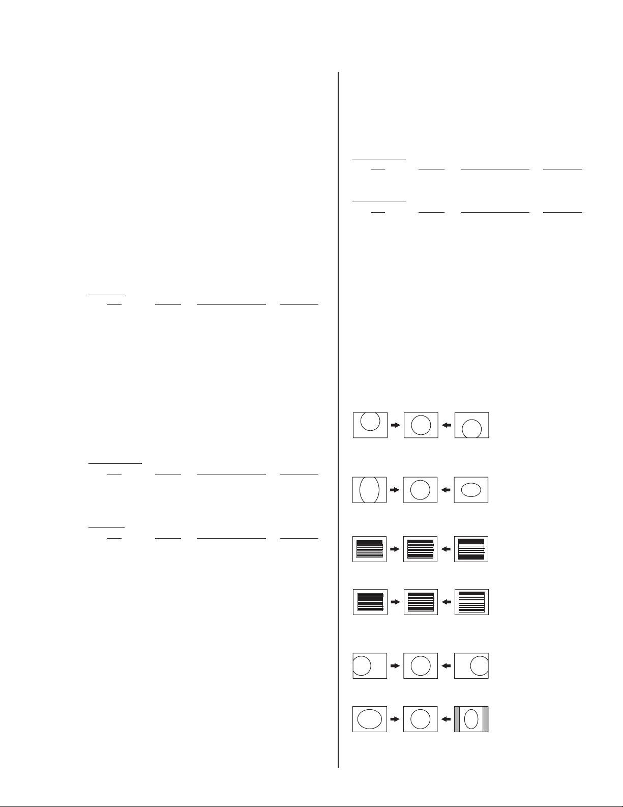
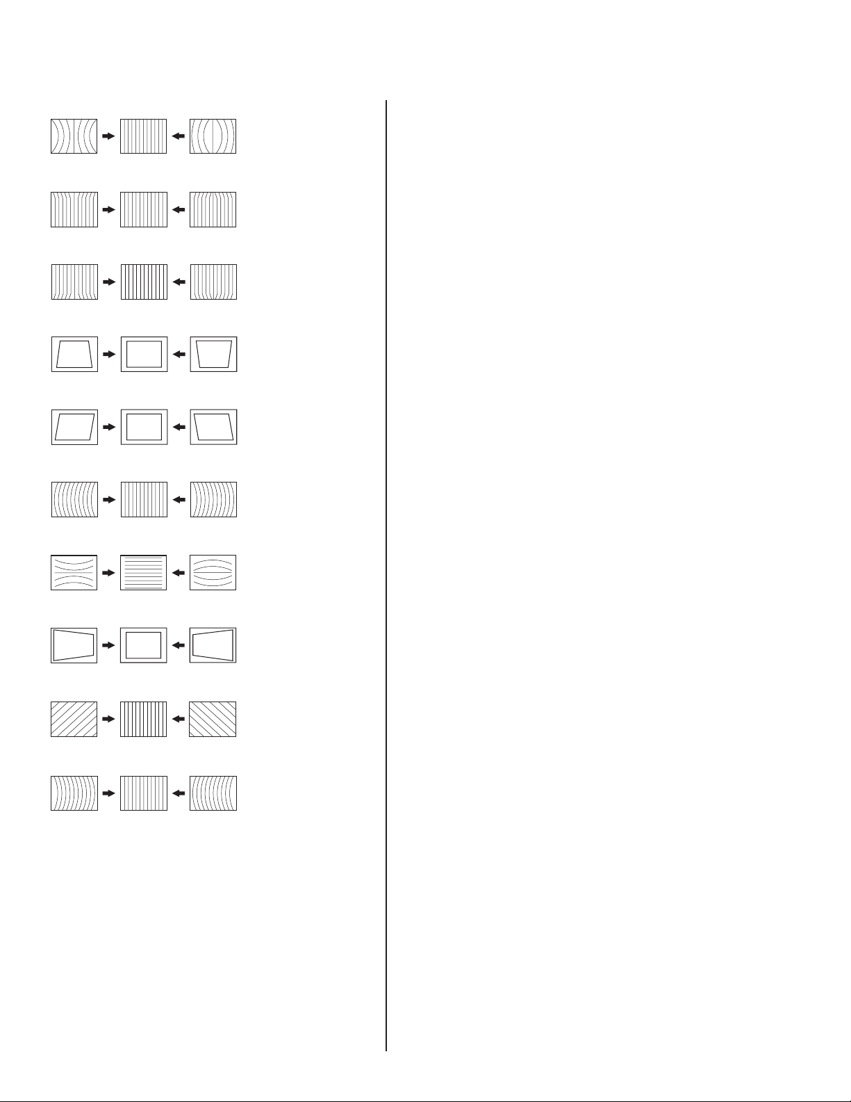
0. VPOS ( V-POSITION)
1. VSIZ (V-SIZE)
2. VLIN (V-LINE)
3. VSCO (VS-COR)
4. HCNT (H-CENTERING)
— 21 —
5. HSIZ (H-SIZE)
KV-32XBR400/36XBR400/38DRC1/38DRC1C
6. PIN (PIN AMP)
7. UCP (UP COR PIN COR)
8. LCP (LOW CO PIN COR)
9. PPHA(PIN PHASE)
10. VANG (AFC-ANGLE)
11. VBOW (AFC-BOW)
12. VPIN (V-PIN)
13. HTPZ (H-TRAPEZOID)
14. LANG (L-ANGLE)
A2150-D1 00 VPOS
A2150-D1 01 VSIZ
0
A2150-D1 02 VLIN
A2150-D1 03 VSCO
A2150-D1 04 VCEN
A2150-D1 05 VPIN
A2150-D1 07 HTPZ
A2150-D2 01 HPOS
A2150-D2 02 HSIZ
A2150-D2 03 SLIN
A2150-D2 05 PIN
A2150-D2 06 UCP
A2150-D2 07 LC P
A2150-D2 13 PPHA
A2150-D2 14 VANG
A2150-D2 15 LANG
A2150-D2 16 VBOW
A2150-D2 17 LBOW
Make sure picture size is within specs. Vertical size is 11.8 sq.
and Horizontal size is 15.8 sq.
4. Write data into memory then set screen to 1080i Mode.
1080i HD mode adjustment
1. Input a 1080i HD cross-hatch signal and an HD monoscope
signal that contains overscan markers.
2. Adjust raster position per section 3-8 only if this procedure
was not performed for full mode.
3. Adjust geometr y similar to Full DRC mode. Ve rtical size is
11.8 sq. and Horizontal size is 15.8 sq if monoscope signal is
available. Otherwise use Vertical size as 91.5% scan,
Horizontal size as 90% scan.
4. Use the following registers to adjust vertical and horizontal
parameters:
A2150-D2 01 HPOS
A2150-D1 05 VPIN
A2150-D1 10 ASPT
A2150-D2 11 SCRL
15. LBOW (L-BOW)
3-10. NTSC (DRC) Full mode adjustment
1. Face picture tube to east or west direction.
2. Complete VPIN and VCEN adjustment first. (A2150-D1 05
VPIN, A2150-D1 04 VCEN)
3. Input a monoscope and a cross-hatch signal. Adjust picture
distortion with the following service parameters to balance
the best condition for these two signals.
If necessary, touch up geometry using the data registers listed
above for Full mode.
5. Write data into memory.
Vertical Compressed Mode Adjustment
1. Input a monoscope and a cross-hatch signal.
2. T ouch up g eometry using the data re gisters listed above f or
Full mode, however no adjustment should be necessary.
Vertical size is 11.8 sq. and Horizontal size is 15.8 sq.
3. Check Full mode for any side effect for any adjustments to
Vertical Compressed mode or 1080i HD mode.
— 22 —
KV-32XBR400/36XBR400/38DRC1/38DRC1C
SECTION 4
SAFETY RELATED ADJUSTMENTS
RV8001, RV8002, RV8003 CONFIRMATION METHOD AND HV SERVICE ADJUSTMENTS
The following adjustments should always be performed when replacing the following components which are marked with on the
schematic diagram:
D BOARD: DY, CRT, IC6503, IC8001, IC8003, IC8004, D8004, D8014, R8016, R8021, R8028, R8041, R8042,
R8044, R8072, R8073, R8074, R8077, R8078, R8080, R8081, R8082, R8091, R8095
B+ Max Confirmation:
Standard: 135.3 + 1 VCD
Check Condition: AC input voltage : 120 (± 2) V A C at Board Adjustment Process
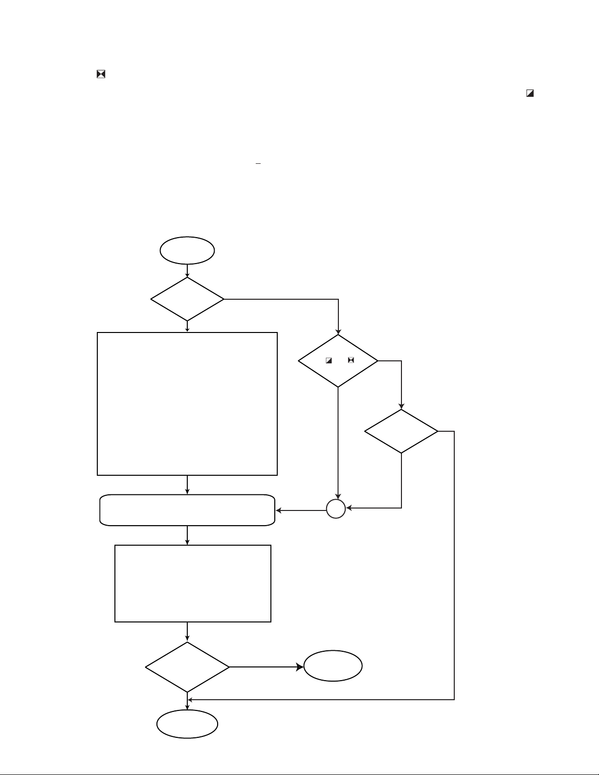
HV Service Flowchart
Start
Is RHT Changed?
Yes
Replace RV8001,RV8002 and RV8003 with same value.
HV protect adjust and inspection
1. Turn RV8001and RV8003 fully counter clockwise.
2. Turn set on with black video signal then adjust RV8002
slowly to obtain 35.5kv.
3. Adjust RV8001 clockwise slowly until hold down
protection just activates, turn off set. Turn back
RV8001 about 1/16 turn; then turn set back on.
4. Turn RV8003 (fine adjust) slowly clockwise until hold
down protect just activates. Then turn the set off.
5. Adjust RV8002 clockwise, then turn the set on. Change
video to white field then slowly turn RV8002 counter
clockwise to get 35.0 ±0.2 kv. Confirm set does NOT
TURN OFF at this condition. If yes then repeat from
step 1 again.
6. Finally, set back RV8002 to 31.50kv ± 0.2kv at video
cut off ( black video).
No
130 ( ± 2) VAC at QC
120 ( ± 2 ) VAC at Overall Adjustment (After aging)
*Note: If using stabilized power supply , make sur e the distortion factor is 3% or less.
Setting Mode: Full mode
Signal input : Cross hatch of NTSC at QC
Initial setting : Reset condition at QC
Confirm point : Across C6544 for B+ of [D] board.
Change any
or
marked parts?
Yes
No
Is D board
replaced?
Yes
No
If all adjustment are finished, then seal and secure
RV8001,RV8002 and RV8003 with epoxy to prevent any
possible misadjustment by non- trained technical service.
Confirm +B, Vd and check Hold down on D
board with black video with the following steps:
1. Confirm +B across C6544 to make sure it is
135.3 ± 1 V dc.
2. Confirm Vd at pin 2 CN6506 or at TP-Vd for
4.9 v < Vd < 5.1 V dc.
3. Apply 5.5 +0.5 VDC at pin 2 of CN6544
then confirm set holds down.
Is +B Vd. and
Hold down
confirmed?
Yes
Finish for
hold-down check
No
Start from
the beginning.
— 23 —
KV-32XBR400/36XBR400/38DRC1/38DRC1C
SECTION 5
CIRCUIT ADJUSTMENTS
ELECTRICAL ADJUSTMENTS BY REMOTE COMMANDER
Use the Remote Commander (RM-Y74) to perform the circuit adjustments in this section.
NOTE: Test Equipment Required:
• Pattern generator
• Frequency counter
• Digital multimeter
• Audio oscillator
5-1. SETTING THE SERVICE ADJUSTMENT MODE
1. Standby mode (power off).
2.
on Remote Commander (press each button within a second).
SERVICE ADJUSTMENT MODE VIEW
Reading the Memory
1. Enter into Service Mode
2. Press on the remote commander.
Adjusting the Picture
1. Enter into Service Mode.
5-2. MEMORY WRITE CONFIRMA TION METHOD
1. After adjustment, remove the power plug from the AC
outlet, then plug it in again.
2. Turn the power switch ON and set to service mode.
3. Call the adjusted items again to confirm they were adjusted
.
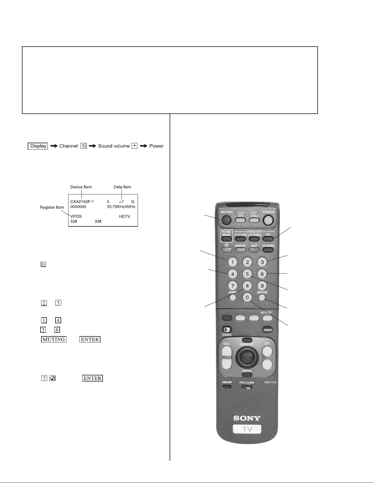
5-3. ADJUSTMENT BUTTONS AND INDICA TORS
WRITE INTO
MEMORY
SERVICE MODE
ITEM UP
ITEM DOWN
DA TA UP
DAT A DOWN
DEVICE ITEM DOWN
2. Press
device item.
2. Press
3. Press
4. Press
or on the Remote Commander to select the
or on the Remote Commander to select an item.
or on the Remote Commander to change the data.
then to save into the memory.
Resetting the Data
1. Enter into Service Mode.
2. Press then press on the Remote
Commander .
— 24 —
INITIALIZE
WRITE INTO MEMORY
REVIEW MEMORY
RM-Y174
KV-27FS12/27FS16/29FS12/29FS12C
IC3048 (Main) / B-board
y
(
)
(
)
IC3048 (Main) / B-board
IC3602 (Main) / B-board
y
(
)
(
)
y
(
)
(
)
Service Control
Device Slave Address & Microprocessor Version
Slave Address: 9Ah
Slave Address: 86h
Slave Address: 86h
, Slave Address: 60h
Patch A
with ROM correction
Version 1.0
stem Micro
S
Slave Address: 9Ah
CCD&Vchip Micro (Version 2.14), Slave Address: 68h (Main)
, Slave Address: 60h
, Slave Address: 60h
Patch A
Patch A
with ROM correction
with ROM correction
Version 1.0
Version 1.0
stem Micro
stem Micro
S
S
DX1A Service List ------ Contents
5-4. SERVICE DATA LISTS
Service Control
IC2004 / BC-board Slave Address: B8h (Write) & B9h (Read)
IC201 / A-board
IC201 / A-board
Device Reference Number
µPD64082
Device Name
Service Control
CXA2103Q
CXA2150Q
CXA2150Q
Service Control
# 1 3D-COMB
Category Number & Name
# 2-1 CXA2103-1 (Main)
# 2-2 CXA2103-2 (Sub) IC3110 (Sub) / B-board Slave Address: 9Eh
# 3-1 CXA2150P-1
# 3-2 CXA2150P-2
# 3-3 CXA2150P-3
# 3-4 CXA2150P-4
# 4-1 CXA2150D-1
# 4-2 CXA2150D-2
# 5 CXA2151 CXA2151Q IC3001 / B-board Slave Address: 84h
# 6 D-CONV CXA8070P IC5513 / D-board Slave Address: DEh
# 7 CXA2026 CXA2026AS IC5511 / D-board Slave Address: 8Eh
# 4-3 CXA2150D-3
# 8 AP BH3868FS IC7001 / A-board Slave Address: 82h
IC2004 / BC-board Slave Address: B8h (Write) & B9h (Read)
IC3601 (Sub) / B-board CCD&Vchip Micro (Version 2.14), Slave Address: 6Ch (Sub)
µPD64082
CXA2150Q IC201 / A-board Slave Address: 86h
CXA2103Q
M306V2ME-150FP IC701 / A-board
OSD
SNNR
CXP85840A-039Q
M306V2ME-150FP IC701 / A-board
M306V2ME-150FP IC701 / A-board
ID
OP
CCD&VCHIP
# 9 TRUS NJM2180M IC4101 / S-board Controlled through CXA1315M ( IC4103 / S-board, Slave Address: 48h )
# 10 MID1 CXD9509AQ IC3408 / B-board Slave Address: 2Eh { Controlled through MID-X Micro ( IC3090 / B-board / 64h ) }
# 11 MID2 CXD9509AQ IC3408 / B-board Slave Address: 2Eh { Controlled through MID-X Micro ( IC3090 / B-board / 64h ) }
# 12 MID3 CXD9509AQ IC3408 / B-board Slave Address: 2Eh { Controlled through MID-X Micro ( IC3090 / B-board / 64h ) }
# 13 MID5 CXD9509AQ IC3408 / B-board Slave Address: 2Eh { Controlled through MID-X Micro ( IC3090 / B-board / 64h ) }
# 14
# 15
# 17
# 16 ID1 CXD2085M IC3603 / B-board Slave Address: 40h
# 18
# 19
Note:
DX1A System Micro & Software: M306V2ME-150FP (MASK), Software Version 1.0 {with ROM correction (Patch A)}, IC701/A-board (Slave Adress: 60h)
DX1A MID-X Micro & Software: MB94918RPF-G-128-BND (MASK1), Software Version 03/30/00, IC3090/B-board (Slave Address: 64h)
MB94918RPF-G-130-BND (MASK2), Software Version 04/20/00, IC3090/B-board (Slave Address: 64h)
DX1A CCD&Vchip Micro Software: CXP85840A-039Q (MASK), Software Version 2.14, IC3602/B-board (Main/Slave Address: 68h) & IC3601/B-board (Sub/Slave Address: 6Ch)
— 25 —
KV-27FS12/27FS16/29FS12/29FS12C
Comment
: CVideo1~4 inputs
: SVideo1~3 inputs
SVideo (SV)
CVideo (CV)
: Common data
C
: YCbCr-480i/480p/1080i inputs
: CVideo1~4 & SVideo1~3 inputs
Data Initial Setting
Data
Data
DX1A SERVICE LIST (#1): 3D-COMB / µPD64082 (Part 1)
Non-
standard
SVideo
Standard
(32V&36V CRTs)
Range
Type
Non-
standard
UHF/VHF & CVideo
Standard
Non-
standard
Standard
Non-
standard
UHF/VHF & CVideo SVideo
Standard
C 0~3 3
C 0~7 3
Video1~4
Video5&6
UHF/VHF Video1~4 Video5&6
0~3 1 1 1
4 (32V) / 8 (36V) {Initial Data: 8 (36V)}
SNNR Setting (-Offset)
SNNR = 0 SNNR = 1 SNNR = 2 SNNR = 3
VAPG1 Data Based on MENU/VM Setting VAPG2 Data Based on SNNR/Offset-setting
VM = Off VM = Low VM = Mid VM = High SNNR = 0 SNNR = 1 SNNR = 2 SNNR = 3
0~3 1 1 1
0~3 2 2 2
Control Register
Function & Link
Selection for standard/non-satndard signal processing 0~3 0 0 0 0
Operation mode setting 0~3 0 1 3 3
Y-output correction
(V-aperture compensation & Y-peaking filtering)
System clock setting C 0~3 1
YAPS
Register
Device Name: µPD64082 { 3D-Comb Filter / NEC } / IC2004 (BC-board)
Slave Address: B8h (Write Address) / B9h (Read Address)
No & Name
NRMD
0
CLKS
1
2
Selection for inter-frame/inter-line processing C 0~3 0
MSS
NSDS
3
4
Killer processing selection C 0~3 1
C-signal phase with respect to the Y-signal
(Fine adjustment at 70 ns/step)
NRMD Setting-based Control Table for DYCO, DYGA, DCCO, DCGA NRMD = 0 NRMD = 1 NRMD = 2 NRMD = 3
DY detection coring level (Y motion detection coring) 0~15 2 2 2 2
DY detection gain (Y motion detection gain) 0~15 10 10 10 10
DC detection coring level (C motion detection coring) 0~15 5 5 5 5
DC detection gain (C motion detection gain) 0~15 5 5 5 5
Frame recersive YNR nonlinear filter limit level C 0~3 1
Frame recersive CNR nonlinear filter limit level C 0~3 1
CDL
KILS
5
DYCO
DYGA
6
7
8
DCCO
DCGA
9
10
YNRL
CNRL
11
12
— 26 —
V-aperture compensation gain 0~7 0 2 3 4 0 0 0 0
Sensitivity for Hsync non-standard signal detection
(out-of-Hsync intra-field)
Sensitivity for frame non-standard signal detection
Hysteresis for Hsync non-standard signal detection
(out-of-Hsync intra-field)
VTRH
13
(out-of-Hsync inter-frame)
VM&SNNR Setting-based Control Table for VAPG & VAPI
LDSR
VTRR
15
14
V-aperture compensation convergence point 0~31 4 4 4
VAPG= VAPG1 - VAPG2
VAPI
VAPG
17
16
Y peaking filter (BPF) gain 0~15 7 0 1 2 3
Y peaking filter (BPF) center frequency 0~3 0 0 0 0 0
SNNR Setting-based Control Table for YPFT & YHFG
YPFT
YPFG
18
19
 Loading...