

SONY KV-29X5R Diagram

HISTORY INFORMATION FOR THE FOLLOWING MANUAL:
SERVICE MANUAL
MODEL NAME REMOTE COMMANDER DESTINATION
KDL-22BX300
KDL-22BX300
KDL-22BX300
KDL-22BX300
KDL-32BX300
KDL-32BX300
KDL-32BX300
RM-YD035 US
RM-YD035 CND
RM-YD035 MX
RM-YD035 LATIN AMERICA
RM-YD035 US
RM-YD035 CND
RM-YD035 MX
AZ1-FK
CHASSIS
LEVEL
CONFIDENTIAL
3
ORIGINAL MANUAL ISSUE DATE: 2/2010
REVISION DATE SUBJECT
2/2010 No revisions or updates are applicable at this time.
LCD DIGITAL COLOR TV
9-883-846-51

KDL-22BX300/32BX300
TABLE OF CONTENTS
SECTION TITLE PAGE
Safety-Related Component Warning ..........................................................................................................................................................................3
Safety Check-Out ....................................................................................................................................................................................................... 5
SECTION 1: DIAGRAMS ................................................................................................................................................................................................... 6
1-1. Circuit Boards Location ...................................................................................................................................................................................... 6
1-2. Printed Wiring Boards and Schematic Diagrams Information ............................................................................................................................ 6
1-3. Block Diagram .................................................................................................................................................................................................... 8
1-4. Schematics and Supporting Information ............................................................................................................................................................9
A Board Schematic Diagram (1 of 15) ................................................................................................................................................................ 9
A Board Schematic Diagram (2 of 15) .............................................................................................................................................................. 10
A Board Schematic Diagram (3 of 15) .............................................................................................................................................................. 11
A Board Schematic Diagram (4 of 15) .............................................................................................................................................................. 12
A Board Schematic Diagram (5 of 15) .............................................................................................................................................................. 13
A Board Schematic Diagram (6 of 15) .............................................................................................................................................................. 14
A Board Schematic Diagram (7 of 15) .............................................................................................................................................................. 15
A Board Schematic Diagram (8 of 15) .............................................................................................................................................................. 16
A Board Schematic Diagram (9 of 15) .............................................................................................................................................................. 17
A Board Schematic Diagram (10 of 15) ............................................................................................................................................................ 18
A Board Schematic Diagram (11 of 15) ............................................................................................................................................................ 19
A Board Schematic Diagram (12 of 15) ............................................................................................................................................................ 20
A Board Schematic Diagram (13 of 15) ............................................................................................................................................................ 21
A Board Schematic Diagram (14 of 15) ............................................................................................................................................................ 22
A Board Schematic Diagram (15 of 15) ............................................................................................................................................................ 23
GD1 (Power) Board Schematic Diagram (1 of 2) (KDL-22BX300 ONLY) ........................................................................................................ 26
GD1 (Power) Board Schematic Diagram (2 of 2) (KDL-22BX300 ONLY) ........................................................................................................ 27
G2LE (Power) Board Schematic Diagram (KDL-32BX300 ONLY) .................................................................................................................. 29
H Board Schematic Diagram ............................................................................................................................................................................ 31
Switch Unit Schematic Diagram ....................................................................................................................................................................... 32
APPENDIX A: ENCRYPTION KEY COMPONENTS ..................................................................................................................................................... A-1
KDL-22BX300/32BX300
2
SAFETY-RELATED COMPONENT WARNING
KDL-22BX300/32BX300
There are critical components used in LCD color TVs that are important for safety. These components are identifi ed with shading and
mark on the schematic diagrams and the electrical parts list. It is essential that these critical parts be replaced only with the part number
specifi ed in the electrical parts list to prevent electric shock, fi re, or other hazard.
NOTE: Do not modify the original design without obtaining written permission from the manufacturer or you will void the original parts and
labor guarantee.
!
USE CAUTION WHEN HANDLING THE LCD PANEL
When repairing the LCD panel, be sure you are grounded by using a wrist band.
When installing the LCD panel on a wall, the LCD panel must be secured using the 4 mounting holes on the rear cover.
To avoid damaging the LCD panel:
do not press on the panel or frame edge to avoid the risk of electric shock.
do not scratch or press on the panel with any sharp objects.
do not leave the module in high temperatures or in areas of high humidity for an extended period of time.
do not expose the LCD panel to direct sunlight.
avoid contact with water. It may cause a short circuit within the module.
disconnect the AC adapter when replacing the backlight (CCFL) or inverter circuit.
(High voltage occurs at the inverter circuit at 650Vrms.)
always clean the LCD panel with a soft cloth material.
use care when handling the wires or connectors of the inverter circuit. Damaging the wires may cause a short.
protect the panel from ESD to avoid damaging the electronic circuit (C-MOS).
LEAKAGE CURRENT HOT CHECK CIRCUIT
KDL-22BX300/32BX300
3
KDL-22BX300/32BX300
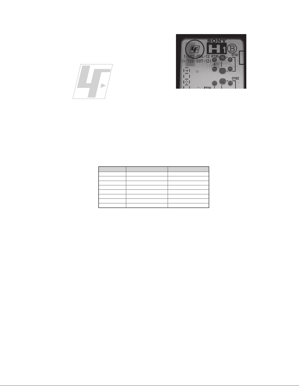
The circuit boards used in these models have been processed using
Lead Free Solder. The boards are identified by the LF logo located
close to the board designation e.g. H1 etc [ see example ]. The
servicing of these boards requires special precautions to be taken as
outlined below.
example
It is strongly recommended to use Lead Free Solder material in order to guarantee optimal quality of new solder joints.
Lead Free Solder is available under the following part numbers :
r e b m u n t r a P r e t e m a i D s k r a m e R
9 1 - 5 0 0 - 0 4 6 - 7m m 3 . 0g K 5 2 . 0
0 2 - 5 0 0 - 0 4 6 - 7m m 4 . 0g K 0 5 . 0
1 2 - 5 0 0 - 0 4 6 - 7m m 5 . 0g K 0 5 . 0
2 2 - 5 0 0 - 0 4 6 - 7m m 6 . 0g K 5 2 . 0
3 2 - 5 0 0 - 0 4 6 - 7m m 8 . 0g K 0 0 . 1
4 2 - 5 0 0 - 0 4 6 - 7m m 0 . 1g K 0 0 . 1
5 2 - 5 0 0 - 0 4 6 - 7m m 2 . 1g K 0 0 . 1
6 2 - 5 0 0 - 0 4 6 - 7m m 6 . 1g K 0 0 . 1
Due to the higher melting point of Lead Free Solder the soldering iron tip temperature needs to be set to 370 degrees centigrade.
This requires soldering equipment capable of accurate temperature control coupled with a good heat recovery characteristics.
For more information on the use of Lead Free Solder, please refer to
http://www.sony-training.com
KDL-22BX300/32BX300
4
SAFETY CHECK-OUT
To E
l
KDL-22BX300/32BX300
After correcting the original service problem, perform the following
safety checks before releasing the set to the customer:
1. Check the area of your repair for unsoldered or poorly soldered
connections. Check the entire board surface for solder splashes and
bridges.
2. Check the interboard wiring to ensure that no wires are “pinched” or
touching high-wattage resistors.
3. Check that all control knobs, shields, covers, ground straps, and
mounting hardware have been replaced. Be absolutely certain that
you have replaced all the insulators.
4. Look for unauthorized replacement parts, particularly transistors,
that were installed during a previous repair. Point them out to the
customer and recommend their replacement.
5. Look for parts which, though functioning, show obvious signs of
deterioration. Point them out to the customer and recommend their
replacement.
6. Check the line cords for cracks and abrasion. Recommend the
replacement of any such line cord to the customer.
7. Check the antenna terminals, metal trim, “metallized” knobs, screws,
and all other exposed metal parts for AC leakage. Check leakage as
described below.
The AC leakage from any exposed metal part to earth ground and
from all exposed metal parts to any exposed metal part having a
return to chassis, must not exceed 0.5 mA (500 microamperes).
Leakage current can be measured by any one of three methods.
1. A commercial leakage tester, such as the Simpson 229 or RCA
WT-540A. Follow the manufacturers’ instructions to use these
instructions.
2. A battery-operated AC milliampmeter. The Data Precision 245
digital multimeter is suitable for this job.
3. Measuring the voltage drop across a resistor by means of a VOM
or battery-operated AC voltmeter. The “limit” indication is 0.75
V, so analog meters must have an accurate low voltage scale.
The Simpson’s 250 and Sanwa SH-63TRD are examples of
passive VOMs that are suitable. Nearly all battery-operated digital
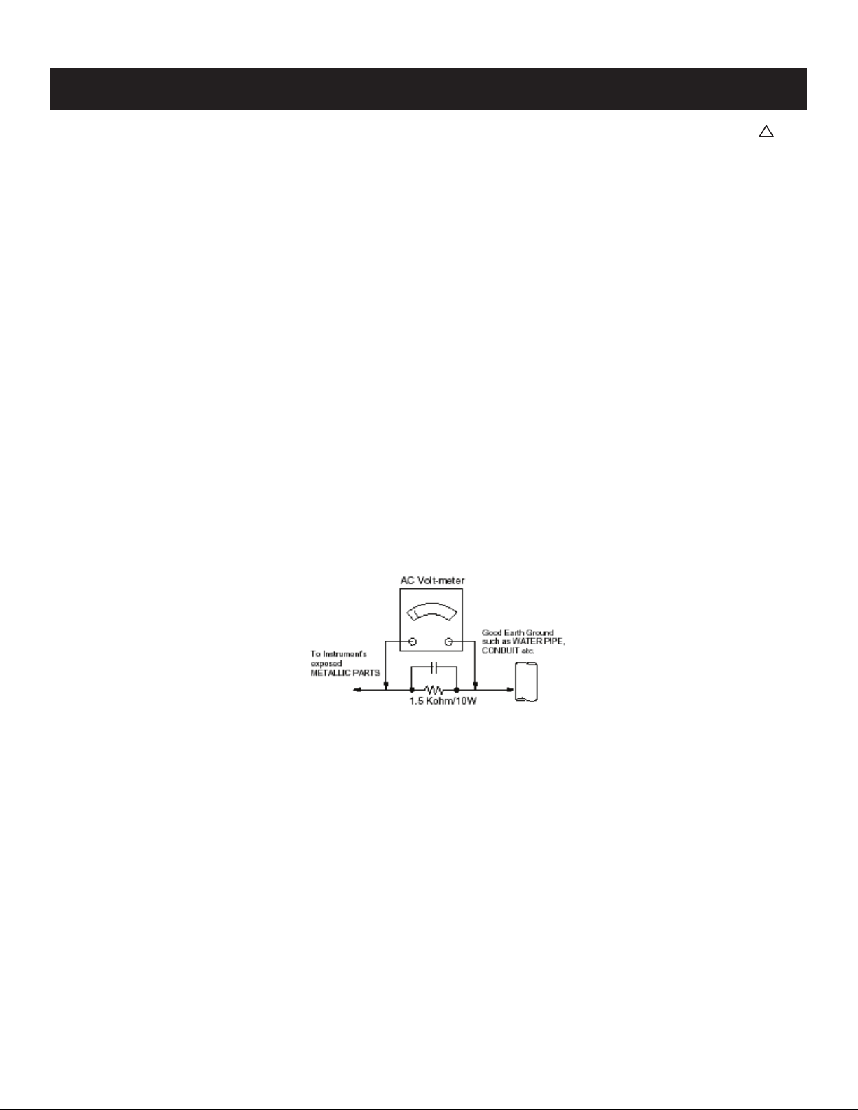
multimeters that have a 2 VAC range are suitable (see Figure A).
How to Find a Good Earth Ground
A cold-water pipe is a guaranteed earth ground; the cover-plate
retaining screw on most AC outlet boxes is also at earth ground. If the
retaining screw is to be used as your earth ground, verify that it is at
ground by measuring the resistance between it and a cold-water pipe
with an ohmmeter. The reading should be zero ohms.
If a cold-water pipe is not accessible, connect a 60- to 100-watt
trouble- light (not a neon lamp) between the hot side of the receptacle
and the retaining screw. Try both slots, if necessary, to locate the hot
side on the line; the lamp should light at normal brilliance if the screw
is at ground potential (see Figure B).
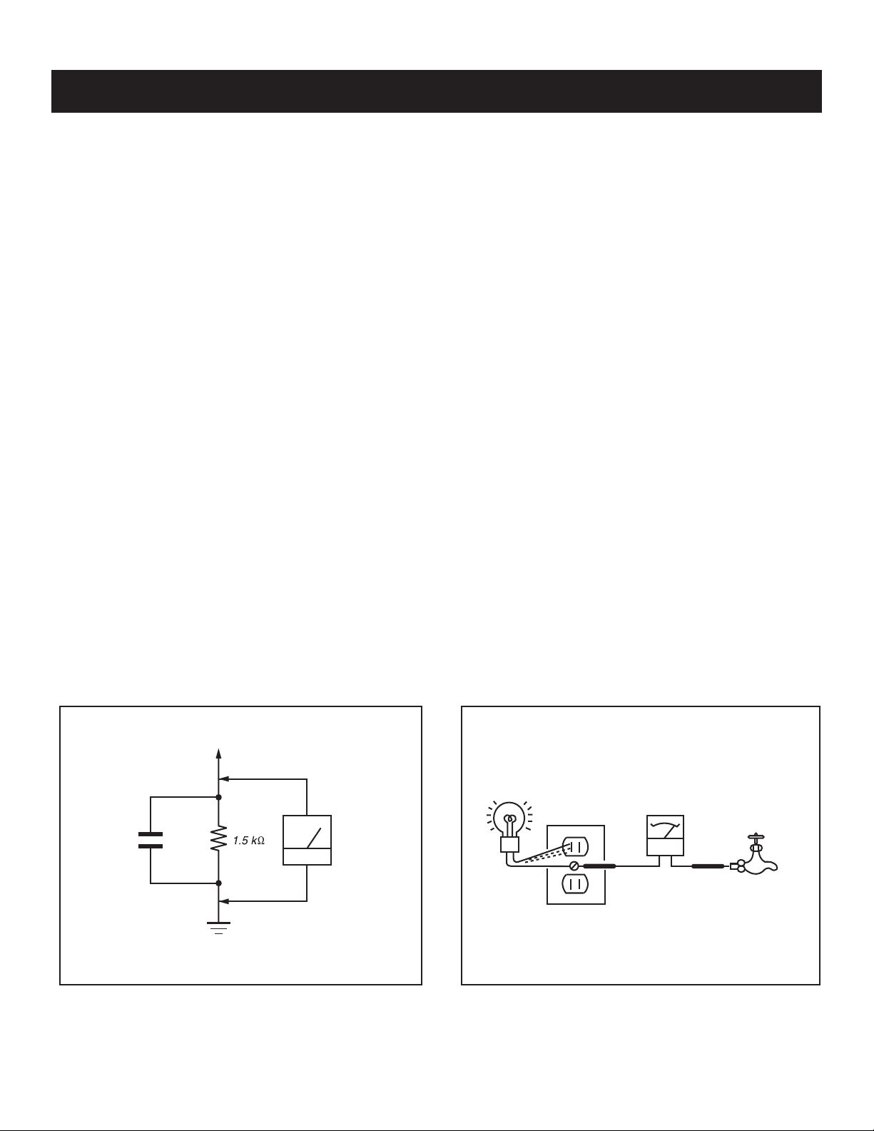
Leakage Test
0.15 μF
Figure A. Using an AC voltmeter to check AC leakage. Figure B. Checking for earth ground.
xposed Meta
Parts on Set
Earth Ground
AC
Voltmeter
(0.75V)
Trouble Light
AC Outlet Box
Ohmmeter
Cold-water Pipe
KDL-22BX300/32BX300
5
1-1. CIRCUIT BOARDS LOCATION
H
KDL-22BX300/32BX300
SECTION 1: DIAGRAMS
A
GD1 (KDL-22BX300 ONLY)
G2LE (KDL-32BX300 ONLY)
SWITCH UNIT
1-2.
PRINTED WIRING BOARDS AND SCHEMATIC DIAGRAMS INFORMATION
All capacitors are in μF unless otherwise noted. pF : μμF 50WV or
less are not indicated except for electrolytics and tantalums.
All electrolytics are in 50V unless otherwise specifi ed.
All resistors are in ohms. k=1000, M=1000k
Indication of resistance, which does not have one for rating
electrical power, is as follows: Pitch : 5mm
Rating electrical power :
1
/
W in resistance, 1/
4
W and 1/
10
W in chip resistance.
16
1
/
4
: nonfl ammable resistor
: fusible resistor
: internal component
: panel designation and adjustment for repair
: earth ground
: earth-chassis
All variable and adjustable resistors have characteristic curve B,
unless otherwise noted.
All voltages are in V.
S : Measurement impossibility.
: B+line.
: B-line. (Actual measured value may be different).
: signal path. (RF)
Circled numbers are waveform references.
W
The components identifi ed by shading and ! symbol are critical for safety. Replace
only with part number specifi ed.
The symbol indicates a fast operating fuse and is displayed on the component
side of the board. Replace only with fuse of the same rating as marked.
Les composants identifi es per un trame et une marque
securite. Ne les remplacer que par une piece portant le numero specifi e.
Le symbole indique une fusible a action rapide. Doit etre remplace par une
fusible de meme yaleur, comme maque.
Readings are taken with a color-bar signal input.
Readings are taken with a 10M digital multimeter.
Voltages are DC with respect to ground unless otherwise noted.
Voltage variations may be noted due to normal production
tolerances.
NOTE: The components identifi ed by a red outline and a mark contain confi dential
information. Specifi c instructions must be adhered to whenever these components
are repaired and/or replaced.
See Appendix A: Encryption Key Components in the back of this manual.
!
sont critiques pour la
KDL-22BX300/32BX300
6
KDL-22BX300/32BX300
REFERENCE INFORMATION
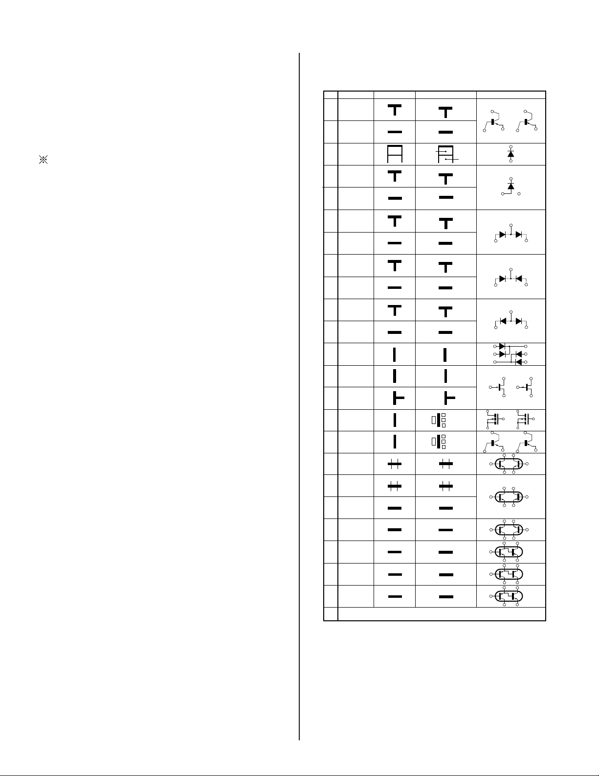
RESISTOR
: RN METAL FILM
: RC SOLID
: FPRD NONFLAMMABLE CARBON
: FUSE NONFLAMMABLE FUSIBLE
: RW NONFLAMMABLE WIREWOUND
: RS NONFLAMMABLE METAL OXIDE
: RB NONFLAMMABLE CEMENT
: ADJUSTMENT RESISTOR
COIL
: LF-8L MICRO INDUCTOR
CAPACITOR
: TA TANTALUM
: PS STYROL
: PP POLYPROPYLENE
: PT MYLAR
: MPS METALIZED POLYESTER
: MPP METALIZED POLYPROPYLENE
: ALB BIPOLAR
: ALT HIGH TEMPERATURE
: ALR HIGH RIPPLE
Terminal name of semiconductors in silk screen
printed circuit ( )
Device Printed symbol Terminal name
Transistor
1
Transistor
2
3
Diode
4
Diode
Diode
5
Diode
6
Diode
7
8
Diode
Diode
9
Diode
10
Diode
11
Diode
12
Transistor
13
(FET)
Transistor
14
(FET)
Transistor
15
(FET)
Transistor
16
Transistor
17
Transistor
18
Transistor
19
Transistor
20
Transistor
21
Transistor
22
Transistor
23
Discrete semiconductor
–
(Chip semiconductors that are not actually used are included.)
*
Collector
Base
Collector
Base
Cathode
Cathode
Anode
Cathode
Anode
Common
Anode
Common
Anode Cathode
Common
Anode
Common
Anode Anode
Common
Cathode
Common
Cathode
Anode
Anode
Cathode
Drain
Drain
B1 E1
C2
B2 C1E2
B2 E2
C1
B1 C2
E1
B2 E2
C1
B1 C2E1
B2 E2
C1
B1 C2E1
E2
B1 E1
C2
(B2)
E1
B1
C1
(B2)
E1
E2
C2
Emitter
Emitter
Anode
(NC)
(NC)
Cathode
Anode
Cathode
Cathode
Cathode
Anode
Anode
Source
Gate
Source
Gate
Source
Drain
Gate
Emitter
Collector
Base
C1(B2)
E2
C2
B1
C1
Circuit
D
G
D
S
B1
B1
B1
B1
B1
B1
D
G
S
S
D
G
C1
E1
C1
E1
E1
C1
E2
C1
C1
G
S
C2
B2
E2
C2
B2
E2
E2
B2
C2
C2C1(B2)
E2
E2E1(B2)
C2
C2E1(B2)
C2
Ver.1.6
KDL-22BX300/32BX300
7
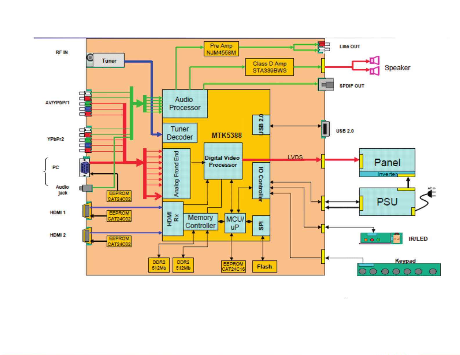
1-3. BLOCK DIAGRAM
KDL-22BX300/32BX300
KDL-22BX300/32BX300
8
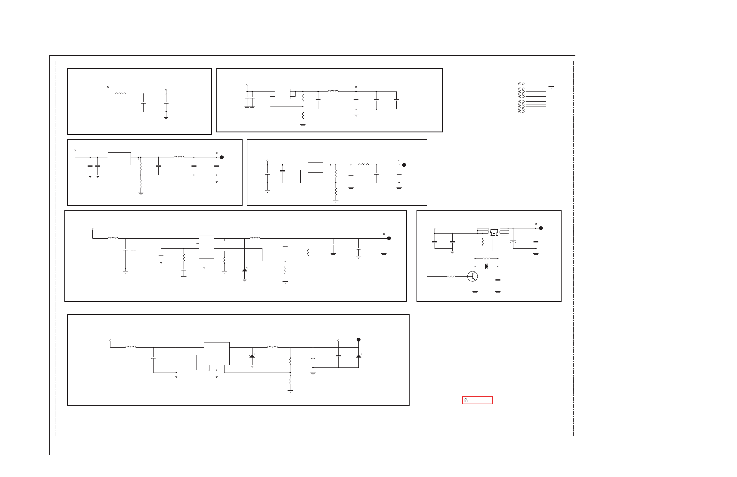
1-4. SCHEMATICS AND SUPPORTING INFORMATION
A BOARD SCHEMATIC DIAGRAM (1 OF 15)
1 | 2 | 3 | 4 | 5 | 6 | 7 | 8 | 9 | 10 | 11 | 12 |
KDL-22BX300/32BX300
A
—
B
—
C
—
D
—
E
—
F
+3V3SB_PWR
DIGITAL POWER DV33
+5V_PWR
3
INPUT
12
12
C237
C237
10U_10V_M
10U_10V_M
0805_X5R
0805_X5R
C27
C27
0.1U_16V_K
0.1U_16V_K
0603_X7R
0603_X7R
+5V
L3 100R-100MHZ_0805L3 100R-100MHZ_0805
Stand By Power
L62 100R-100MHZ_0805L62 100R-100MHZ_0805
12
C192
C192
10U_10V_M
10U_10V_M
0805_X5R
0805_X5R
U29
U29
2
OUTPUT
4
12
4
ADJ/GND
AZ1084S-ADJTRE1
AZ1084S-ADJTRE1
1
null
null
R27
R27
110_F
110_F
0603
0603
12
R3251
R3251
180_F
180_F
0603
0603
Core Power 1.1V
12
12
C19
C19
C18
C18
0.1U_50V_K
10U_16V_K
10U_16V_K
1206_X7R
1206_X7R
0.1U_50V_K
0603_X7R
0603_X7R
+3V3SB
12
C2
C2
0.1U_16V_K
0.1U_16V_K
0603_X7R
0603_X7R
L79 100R-100MHZ_0805L79 100R-100MHZ_0805
12
C22
C22
10U_10V_M
10U_10V_M
0805_X5R
0805_X5R
12
C14
C14
NC_0.1U_16V_K
NC_0.1U_16V_K
0603_X7R
0603_X7R
12
R3252
R3252
36K_F
36K_F
0402
0402
12
C612
C612
330P_16V_J
330P_16V_J
0402_NP0
0402_NP0
DV33
1
12
C21
C21
10U_10V_M
10U_10V_M
0805_X5R
0805_X5R
4
3
1
null U34
null
IN
LX_1
LX_2
EN
COMP
FREQ
GND
G5682P11U
G5682P11U
2
12
U34
5
6
8
FB
7
(RP5=36K , SW Freq=1.4MHz)
TP227TP227
C26
C26
0.1U_16V_K
0.1U_16V_K
0603_X7R
0603_X7R
12
R3253
R3253
30K_J
30K_J
0402
0402
ANALOG POWER AV33
+5V_PWR
12
12
C235
C235
C236
10U_10V_M
10U_10V_M
0805_X5R
0805_X5R
C236
0.1U_16V_K
0.1U_16V_K
0603_X7R
0603_X7R
10U_10V_M
10U_10V_M
0805_X5R
0805_X5R
L1
L1
1.5UH_3.3A_0.038R
1.5UH_3.3A_0.038R
VLC5020T-1R5N
VLC5020T-1R5N
1 2
21
D2
B340BD2B340B
C181
C181
AV33
12
U27
U27
OUT
VIN
VOUT
ADJ
FR1117-R3GTR
FR1117-R3GTR
null
null
2
12
4
R3249
R3249
12
C12
C12
110_F
110_F
10U_10V_M
10U_10V_M
0805_X5R
0805_X5R
0603
0603
12
R3250
R3250
180_F
180_F
0603
0603
3
1
ANALOG POWER AV125
U1
U1
3
VIN
12
C9
C9
0.1U_16V_K
0.1U_16V_K
0603_X7R
0603_X7R
12
C160
C160
NC_0.1U_16V_K
NC_0.1U_16V_K
0603_X7R
0603_X7R
12
R336
R336
20K_F
20K_F
0603
0603
(0.8 x (1+7.5K/20K) = 1.1V)
1
ADJ
FR1117-R3GTR
FR1117-R3GTR
null
null
12
R3254
R3254
7.5K_F
7.5K_F
0603
0603
OUT
VOUT
L27 100R-100MHZ_0805L27 100R-100MHZ_0805
2
12
4
R3
R3
100_F
100_F
0603
0603
12
R4
R4
0_J
0_J
0603
0603
12
C95
C95
0.1U_16V_K
0.1U_16V_K
0603_X7R
0603_X7R
AV33
12
C15
C15
0.1U_16V_K
0.1U_16V_K
0603_X7R
0603_X7R
L65 100R-100MHZ_0805L65 100R-100MHZ_0805
12
C182
C182
10U_10V_M
10U_10V_M
0805_X5R
0805_X5R
DV11
12
CAP13
CAP13
+
+
220U_16V_M
220U_16V_M
6.3x11
6.3x11
12
C31
C31
10U_10V_M
10U_10V_M
0805_X5R
0805_X5R
12
C10
C10
0.1U_16V_K
0.1U_16V_K
0603_X7R
0603_X7R
DV11
1
12
TP229TP229
C13
C13
10U_10V_M
10U_10V_M
0805_X5R
0805_X5R
12
C53
C53
10U_10V_M
10U_10V_M
0805_X5R
0805_X5R
AV125
1
12
TP228TP228
C11
C11
1U_16V_K
1U_16V_K
0603_X7R
0603_X7R
C239
C239
10U_16V_K
10U_16V_K
1206_X7R
1206_X7R
+5V
DV11
12
1U_16V_K
1U_16V_K
0603_X7R
0603_X7R
12
C240
C240
R254 10K_J 0603R254 10K_J 0603
1
2
1
R252
R252
10K_J
10K_J
0603
0603
R253 470K_J 0603R253 470K_J 0603
C
C
B
B
Q11
Q11
E
E
MMBT3904
MMBT3904
2 3
1
2
3
12
1
D50
D50
1
B0530WS-7-F
B0530WS-7-F
null
null
+12V
Q10
Q10
P2003EVG
P2003EVG
null
null
S
S
4
2
2
GND
+5V_PWR
+3V3SB_PWR
+3V3SB
DV11
DV33
AV33
AV125
+5V
5
6
D
D
7
8
G
G
12
C243
C243
0.01U_25V_K
0.01U_25V_K
0603_X7R
0603_X7R
+5V_PWR+5V_PWR
12
+
CAP24
+
CAP24
NC_220U_16V_M
NC_220U_16V_M
6.3x11
6.3x11
GND
+5V_PWR
+3V3SB_PWR
+3V3SB
DV11
DV33
AV33
AV125
+5V
+12V
+5V_PWR
1
12
C244
C244
0.1U_50V_K
0.1U_50V_K
0603_X7R
0603_X7R
TP231TP231
—
G
—
H
—
I
—
KDL-22BX300/32BX300
+12V
L14 100R-100MHZ_0805L14 100R-100MHZ_0805
12
+
+
CAP20
CAP20
470U_16V_M
470U_16V_M
8x11.5
8x11.5
12
C28
C28
0.1U_50V_K
0.1U_50V_K
0603_X7R
0603_X7R
U2
U2
FP6346-T6GTR null
FP6346-T6GTR null
1
VIN
6
GND_2
SD
5
OUT
GND_13FB
L2
L2
33UH_3A_0.0648R
33UH_3A_0.0648R
SCDS127T-330M-N
2
4
21
SCDS127T-330M-N
1 2
D3
B340BD3B340B
12
12
R338
R338
3.09K_F
3.09K_F
0603
0603
R337
R337
1K_F
1K_F
0603
0603
12
CAP14
CAP14
+
+
220U_16V_M
220U_16V_M
6.3x11
6.3x11
+5V
12
C96
C96
0.1U_16V_K
0.1U_16V_K
0603_X7R
0603_X7R
TP230TP230
1
21
D88
D88
LLZ5235B
LLZ5235B
null
null
A 1/15
DIGITAL/ANALOG POWER
1-857-611-11 <AZ1FK> A-P1
9
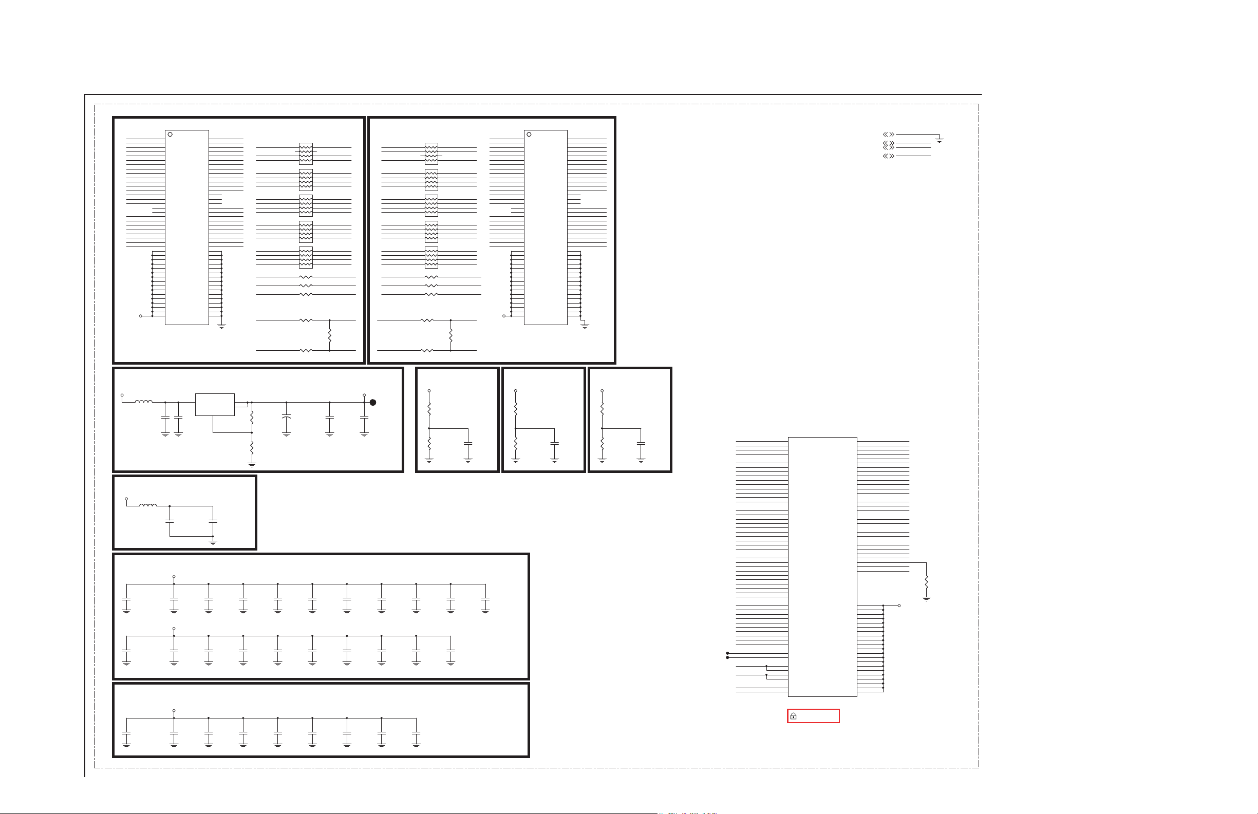
A BOARD SCHEMATIC DIAGRAM (2 OF 15)
1 | 2 | 3 | 4 | 5 | 6 | 7 | 8 | 9 | 10 | 11 | 12 |
KDL-22BX300/32BX300
A
—
B
—
C
—
D
—
E
—
F
—
G
—
H
—
I
U22
U22
G8
DDRV
RDQ16
RDQ17
RDQ18
RDQ19
RDQ20
RDQ21
RDQ22
RDQ23
RDQ24
RDQ25
RDQ26
RDQ27
RDQ28
RDQ29
RDQ30
RDQ31
RDQS3
RDQS3#
RDQS2
RDQS2#
RDQM3
RDQM2
RVREF2
2_CKE
DQ0
G2
DQ1
H7
DQ2
H3
DQ3
H1
DQ4
H9
DQ5
F1
DQ6
F9
DQ7
C8
DQ8
C2
DQ9
D7
DQ10
D3
D1
D9
B1
B9
A2
E2
B7
A8
F7
E8
B3
F3
J2
K2
A1
A9
C1
C3
C7
C9
E1
E9
G1
G3
G7
G9
J1
J9
R1
A10/AP
DQ11
DQ12
DQ13
NC_6
NC_4
DQ14
DQ15
NC_5
NC_1
NC_2
UDQS
NC_3
UDQS#
LDQS
LDQS#
UDM
CAS#
LDM
ODT
VREF
RAS#
CKE
WE#
VDD_1
VSS_1
VSSQ_1
VDDQ_1
VSSQ_2
VDDQ_2
VDDQ_3
VSSQ_3
VDDQ_4
VSSQ_4
VSSQ_5
VDDQ_5
VDD_2
VSS_2
VSSQ_6
VDDQ_6
VSSQ_7
VDDQ_7
VSSQ_8
VDDQ_8
VDDQ_9
VSSQ_9
VDDQ_10
VSSQ_10
VSS_3
VDDL
VDD_3
VSSDL
VDD_4M9VSS_4
VSS_5
VDD_5
SDRAM_BGA-84_512MB
SDRAM_BGA-84_512MB
NT5TU32M16CG-25C
NT5TU32M16CG-25C
DDR#2 DDR#1
DRAM POWER DDRV
L67 100R-100MHZ_0805L67 100R-100MHZ_0805
C338
C338
10U_10V_M
10U_10V_M
0805_X5R
0805_X5R
AV125
AV12_MEMPLL
L69 100R-100MHZ_0805L69 100R-100MHZ_0805
DRAM DE-CAP.
[ RESERVE ]
12
C340
C340
NC_10U_10V_M
NC_10U_10V_M
0805_X5R
0805_X5R
[ RESERVE ]
12
C341
C341
NC_10U_10V_M
NC_10U_10V_M
0805_X5R
0805_X5R
12
12
C32
C32
1U_16V_K
1U_16V_K
0603_X7R
0603_X7R
AVSS12_MEMPLL
DDRV
12
DDRV
12
3
12
C23
C23
0.1U_16V_K
0.1U_16V_K
0603_X7R
0603_X7R
AV12_MEMPLL
C34
C34
4.7U_10V_K
4.7U_10V_K
0603_X5R
0603_X5R
C44
C44
4.7U_10V_K
4.7U_10V_K
0603_X5R
0603_X5R
INPUT
MT5388 DE-CAP.
DDRV
12
C339
C339
10U_10V_M
10U_10V_M
0805_X5R
0805_X5R
12
C54
C54
4.7U_10V_K
4.7U_10V_K
0603_X5R
0603_X5R
A0
A1
A2
A3
A4
A5
A6
A7
A8
A9
A11
A12
BA0
BA1
CK
CK#
CS#
12
12
12
M8
2_A0
M3
2_A1
M7
2_A2
N2
2_A3
N8
2_A4
N3
2_A5
N7
2_A6
P2
2_A7
P8
2_A8
P3
2_A9
M2
2_A10
P7
2_A11
R2
2_A12
R8
R3
R7
L2
2_BA0
L3
2_BA1
L1
2_BA2
J8
CLK1
K8
CLK1#
L8
2_CS#
L7
2_CAS#
K9
2_ODT
K7
2_RAS#
K3
2_WE#
A3
A7
B2
B8
D2
D8
E3
E7
F2
F8
H2
H8
J3
J7
N1
P9
U24
U24
2
OUTPUT
4
4
ADJ/GND
AZ1084S-ADJTRE1
AZ1084S-ADJTRE1
1
null
null
12
C33
C33
0.01U_16V_K
0.01U_16V_K
0402_X7R
0402_X7R
C65
C65
1U_16V_K
1U_16V_K
0603_X7R
0603_X7R
C45
C45
1U_16V_K
1U_16V_K
0603_X7R
0603_X7R
C55
C55
1U_16V_K
1U_16V_K
0603_X7R
0603_X7R
Damping for DDR#2 ADDR/CMD
NEAR BRANCH
2_A0
2_A8 RA8
2_A11
2_A3
2_A10
2_A1
2_BA2
2_BA0
2_BA1
2_CKE
2_WE#
2_A4
2_A6
2_A2
2_CAS#
2_A9
2_A12
2_A7
2_A5 RA5
RCS#
RRAS#
RODT
RCLK1
RCLK1#
12
R20
R20
110_F
110_F
0603
0603
12
R24
R24
48.7_F
48.7_F
0603
0603
12
C36
C36
0.1U_16V_K
0.1U_16V_K
0402_X7R
0402_X7R
12
C46
C46
0.1U_16V_K
0.1U_16V_K
0402_X7R
0402_X7R
12
C56
C56
0.1U_16V_K
0.1U_16V_K
0402_X7R
0402_X7R
1
RP2
RP2
2
3
4
56R 0804_8P4R
56R 0804_8P4R
1
RP4
RP4
2
3
4
56R 0804_8P4R
56R 0804_8P4R
1
RP6
RP6
2
3
4 5
56R 0804_8P4R
56R 0804_8P4R
1
RP8
RP8
2
3
4 5
56R 0804_8P4R
56R 0804_8P4R
1
RP10
RP10
2
3
4
56R 0804_8P4R
56R 0804_8P4R
1 2
R8 56_J0402R8 56_J0402
1
R10 56_J0402R10 56_J0402
1 2
R29 56_J0402R29 56_J0402
1 2
R14 22_J
R14 22_J
R18 22_J
R18 22_J
1
12
CAP56
CAP56
+
+
560U_4V_M
560U_4V_M
8x8
8x8
12
C37
C37
0.1U_16V_K
0.1U_16V_K
0402_X7R
0402_X7R
12
C47
C47
0.1U_16V_K
0.1U_16V_K
0402_X7R
0402_X7R
12
C57
C57
0.1U_16V_K
0.1U_16V_K
0402_X7R
0402_X7R
0402
0402
0402
0402
12
12
12
8
7
6
5
8
7
6
5
8
7
6
8
7
6
8
7
6
5
2
NEAR DRAMNEAR IC
2
C38
C38
0.1U_16V_K
0.1U_16V_K
0402_X7R
0402_X7R
C48
C48
0.1U_16V_K
0.1U_16V_K
0402_X7R
0402_X7R
C58
C58
0.1U_16V_K
0.1U_16V_K
0402_X7R
0402_X7R
12
12
RA0
RA11
RA3
RA10
RA1
RBA2
RBA0
RBA1
RCKE
RWE#
RA4
RA6
RA2
RCAS#
RA9
RA12
RA7
2_CS#
2_RAS#
2_ODT
CLK1
R16
R16
100_F
100_F
0402
0402
CLK1#
C24
C24
1U_16V_K
1U_16V_K
0603_X7R
0603_X7R
12
C39
C39
0.1U_16V_K
0.1U_16V_K
0402_X7R
0402_X7R
12
C49
C49
0.1U_16V_K
0.1U_16V_K
0402_X7R
0402_X7R
12
C59
C59
0.1U_16V_K
0.1U_16V_K
0402_X7R
0402_X7R
Damping for DDR#1 ADDR/CMD
NEAR BRANCH
1_A11
RP3
RP3
1_A0
56R 0804_8P4R
56R 0804_8P4R
56R
56R
1_A5
1_A7
1_A9
1_A12 RA12
RP5
1_CAS#
RP7
RP7
1_A2
1_A6
1_A4
56R 0804_8P4R
56R 0804_8P4R
1_BA2
1_A1
1_A10
1_A3
1_WE#
1_CKE
1_BA1
1_BA0
RCS#
R9 56_J0402R9 56_J0402
RRAS#
R11 56_J0402R11 56_J0402
RODT
R31 56_J0402R31 56_J0402
RCLK0
RCLK0#
DDRVDV33
1
TP234TP234
12
C25
C25
NC_0.1U_16V_K
NC_0.1U_16V_K
0603_X7R
0603_X7R
12
C40
C40
0.1U_16V_K
0.1U_16V_K
0402_X7R
0402_X7R
12
C50
C50
0.1U_16V_K
0.1U_16V_K
0402_X7R
0402_X7R
12
C60
C60
0.1U_16V_K
0.1U_16V_K
0402_X7R
0402_X7R
1
2
3
4 5
4 5
3
2
1
1
2
3
4 5
8
7
6
5
8
7
6
1 2
1 2
1 2
NEAR IC
1 2
R15
R15
22_J
22_J
0402
0402
R19
R19
22_J
22_J
1 2
0402
0402
12
12
12
C41
C41
0.1U_16V_K
0.1U_16V_K
0402_X7R
0402_X7R
12
C51
C51
0.1U_16V_K
0.1U_16V_K
0402_X7R
0402_X7R
12
C61
C61
0.1U_16V_K
0.1U_16V_K
0402_X7R
0402_X7R
R3242
R3242
1K_F
1K_F
0402
0402
R3243
R3243
1K_F
1K_F
0402
0402
8
7
6
6
7
8
8
7
6
1
RP9
RP9
2
3
4
1
RP11
RP11
2
3
45
RA11
RA81_A8
RA0
RA5
RA7
RA9
0804_8P4RRP5
0804_8P4R
RCAS#
RA2
RA6
RA4
RBA2
RA1
RA10
RA3
56R0804_8P4R
56R0804_8P4R
RWE#
RCKE
RBA1
RBA0
56R0804_8P4R
56R0804_8P4R
1_CS#
1_RAS#
1_ODT
NEAR DRAM
CLK0
12
R17
R17
100_J
100_J
0402
0402
CLK0#
12
12
C42
C42
0.1U_16V_K
0.1U_16V_K
0402_X7R
0402_X7R
12
C52
C52
0.1U_16V_K
0.1U_16V_K
0402_X7R
0402_X7R
C177
C177
0.1U_16V_K
0.1U_16V_K
0402_X7R
0402_X7R
12
RDQ0
RDQ1
RDQ2
RDQ3
RDQ4
RDQ5
RDQ6
RDQ7
RDQ8
RDQ9
RDQ10
RDQ11
RDQ12
RDQ13
RDQ14
RDQ15
RDQS1
RDQS1#
RDQS0
RDQS0#
RDQM1
RDQM0
RVREF1
1_CKE
DDRV
C43
C43
0.1U_16V_K
0.1U_16V_K
0402_X7R
0402_X7R
U23
U23
G8
DQ0
G2
DQ1
H7
DQ2
H3
DQ3
H1
DQ4
H9
DQ5
F1
DQ6
F9
DQ7
C8
DQ8
C2
DQ9
D7
DQ10
D3
DQ11
D1
DQ12
D9
DQ13
B1
DQ14
B9
DQ15
A2
NC_1
E2
NC_2
B7
UDQS
A8
UDQS#
F7
LDQS
E8
LDQS#
B3
UDM
F3
LDM
J2
VREF
K2
CKE
A1
VDD_1
A9
VDDQ_1
C1
VDDQ_2
C3
VDDQ_3
C7
VDDQ_4
C9
VDDQ_5
E1
VDD_2
E9
VDDQ_6
G1
VDDQ_7
G3
VDDQ_8
G7
VDDQ_9
G9
VDDQ_10
J1
VDDL
J9
VDD_3
VDD_4M9VSS_4
R1
VDD_5
SDRAM_BGA-84_512MB
SDRAM_BGA-84_512MB
NT5TU32M16CG-25C
NT5TU32M16CG-25C
DDRVDDRV
12
R3244
R3244
1K_F
1K_F
0402
0402
12
R3245
R3245
1K_F
1K_F
0402
0402
A10/AP
NC_6
NC_4
NC_5
NC_3
CAS#
ODT
RAS#
WE#
VSS_1
VSSQ_1
VSSQ_2
VSSQ_3
VSSQ_4
VSSQ_5
VSS_2
VSSQ_6
VSSQ_7
VSSQ_8
VSSQ_9
VSSQ_10
VSS_3
VSSDL
VSS_5
12
M8
A0
M3
A1
M7
A2
N2
A3
N8
A4
N3
A5
N7
A6
P2
A7
P8
A8
P3
A9
M2
P7
A11
R2
A12
R8
R3
R7
L2
BA0
L3
BA1
L1
J8
CK
K8
CK#
L8
CS#
L7
K9
K7
K3
A3
A7
B2
B8
D2
D8
E3
E7
F2
F8
H2
H8
J3
J7
N1
P9
C178
C178
0.1U_16V_K
0.1U_16V_K
0402_X7R
0402_X7R
1_A0
1_A1
1_A2
1_A3
1_A4
1_A5
1_A6
1_A7
1_A8
1_A9
1_A10
1_A11
1_A12
1_BA0
1_BA1
1_BA2
CLK0
CLK0#
1_CS#
1_CAS#
1_ODT
1_RAS#
1_WE#
RA12
RA11
RA10
RA9
RA8
RA7
RA6
RA5
RA4
RA3
RA2
RA1
RA0
RBA0
RBA1
RBA2
RCLK1
RCLK1#
RCLK0
RCLK0#
RCS#
RRAS#
RCAS#
RWE#
RODT
RCKE
DDRV
DV33
AV125
DDRV
GND
12
R23
R23
100_J
100_J
0402
0402
GND3,5,6,7,8,9,10,11,12,13,14,15,16,17
DV333,5,6,8,12,13,15,16,17
AV1253,5,7,8,13,16
DDRV16
MT5388 RVREFDDR1 RVREF DDR2 RVREF
DDRV
12
R3247
R3247
1K_F
1K_F
0402
0402
RVREF3RVREF2RVREF1
12
R3246
R3246
1K_F
1K_F
0402
0402
12
C183
C183
0.1U_16V_K
0.1U_16V_K
0402_X7R
0402_X7R
TP73TP73
TP74TP74
1
1
AV12_MEMPLL
AVSS12_MEMPLL
RDQM0
RDQM1
RDQM2
RDQM3
RDQ0
RDQ1
RDQ2
RDQ3
RDQ4
RDQ5
RDQ6
RDQ7
RDQS0
RDQS0#
RDQ8
RDQ9
RDQ10
RDQ11
RDQ12
RDQ13
RDQ14
RDQ15
RDQS1
RDQS1#
RDQ16
RDQ17
RDQ18
RDQ19
RDQ20
RDQ21
RDQ22RDQ22
RDQ23
RDQS2
RDQS2#
RDQ24
RDQ25
RDQ26
RDQ27
RDQ28
RDQ29
RDQ30
RDQ31
RDQS3
RDQS3#
MEMTP
MEMTN
RVREF3
RVREF3
U3B
U3B
J23
RDQM0
J22
RDQM1
C15
RDQM2
D15
RDQM3
F25
RDQ0
L24
RDQ1
E24
RDQ2
L25
RDQ3
L26
RDQ4
E25
RDQ5
K24
RDQ6
F24
RDQ7
J25
RDQS0
J26
RDQS0_
G22
RDQ8
K25
RDQ9
G23
RDQ10
K23
RDQ11
K22
RDQ12
F23
RDQ13
J24
RDQ14
G24
RDQ15
G25
RDQS1
G26
RDQS1_
D12
RDQ16
C17
RDQ17
C12
RDQ18
B18
RDQ19
A18
RDQ20
B12
RDQ21
B17
RDQ22
E12
RDQ23
B16
RDQS2
A16
RDQS2_
D13
RDQ24
D16
RDQ25
C13
RDQ26
E15
RDQ27
E16
RDQ28
B13
RDQ29
C16
RDQ30
E13
RDQ31
B14
RDQS3
A14
RDQS3_
E21
MEMTP
D21
MEMTN
H17
AVDD12_MEMPLL_2
J17
AVDD12_MEMPLL_1
J16
AVSS12_MEMPLL_1
H16
AVSS12_MEMPLL_2
E17
MEM_VREF_2
D17
MEM_VREF_1
MT5388JFMG
MT5388JFMG
null
null
RA12
RA11
RA10
RBA0
RBA1
RBA2
RCLK1
RCLK1_
RCLK0
RCLK0_
RCS_
RRAS_
RCAS_
RWE_
REXTDN
RODT
RCKE
VCC2IO_2
VCC2IO_3
VCC2IO_4
VCC2IO_5
VCC2IO_6
VCC2IO_7
VCC2IO_8
VCC2IO_9
VCC2IO_10
VCC2IO_11
VCC2IO_12
VCC2IO_13
VCC2IO_14
VCC2IO_15
VCC2IO_16
VCC2IO_17
VCC2IO_18
VCC2IO_19
VCC2IO_1
VCC2IO_20
VCC2IO_21
C25
C18
A23
B26
RA9
D20
RA8
A25
RA7
C21
RA6
A24
RA5
B20
RA4
B24
RA3
D22
RA2
B23
RA1
C20
RA0
B22
C22
C23
A12
A11
E26
D26
E20
E18
A20
B21
B11
D18
A21
A10
B10
C11
D11
E11
E19
A19
B19
C19
D19
F22
L22
E23
L23
D24
D25
M25
C26
M26
C10
M24
A 2/15
DRAM
—
KDL-22BX300/32BX300
1-857-611-11 <AZ1FK> A-P2
10
 Loading...