

Page 1
Self Diagnosis
Supported model
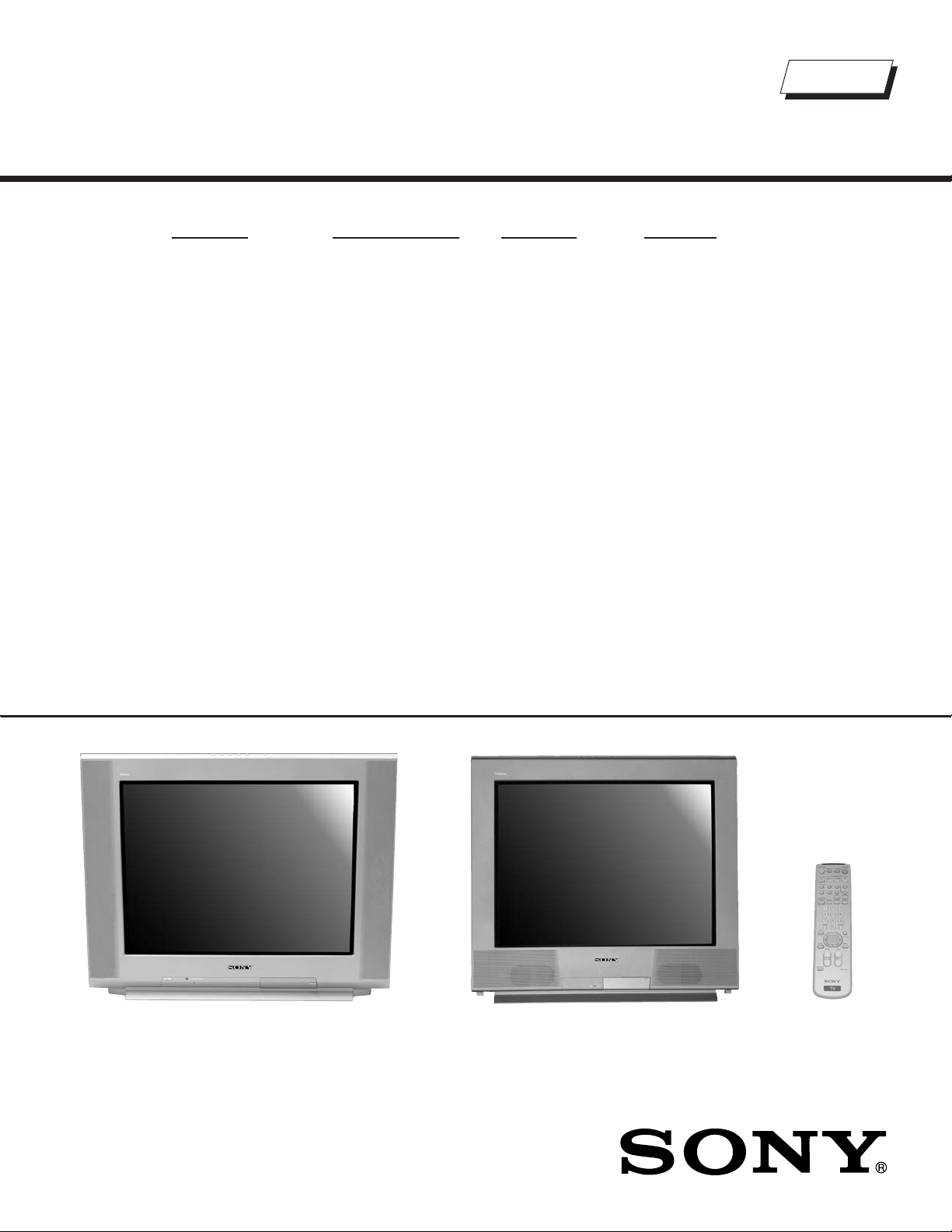
SERVICE MANUAL
MODEL NAME REMOTE COMMANDER DESTINATION CHASSIS NO.
KV -27FS13
KV -27FS13
KV -27FS17
KV -27FV17
KV -27FV17
KV -29FV17
KV -29FV17C
KV -32FS13
KV -32FS13
KV -32FS17
RM-Y180 USA SCC-S40NA
RM-Y180 CND SCC-S41LA
RM-Y181 USA SCC-S40PA
RM-Y181 USA SCC-S40MA
RM-Y181 CND SCC-S41KA
RM-Y181 E SCC-S38XA
RM-Y181 E SCC-S38YA
RM-Y180 USA SCC-S40QA
RM-Y180 CND SCC-S41MA
RM-Y181 USA SCC-S40RA
BA-5
CHASSIS
KV -34FS13C
KV -34FS17
KV-27FV17 KV-27FS17
RM-Y180 E SCC-S56DA
RM-Y181 E SCC-S56JA
RM-Y181
9-965-911-03
TRINITRON® COLOR TELEVISION
Page 2

KV-27FS13/ 27FS17/ 27FV17/ 29FV17/ 29FV17C/ 32FS13/ 32FS17/ 34FS13C/ 34FS17
TABLE OF CONTENTS
SECTION TITLE PAG E
Specifi cations....................................................................................................................................... 3
Warnings and Cautions........................................................................................................................4
Safety Check-Out.................................................................................................................................5
Self-Diagnostic Function......................................................................................................................6
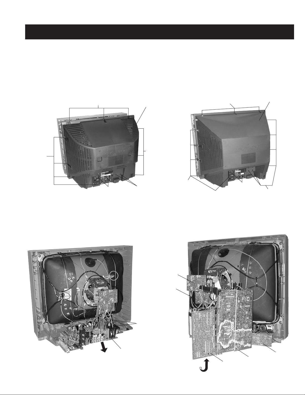
1. Disassembly
1-1. Rear Cover Removal.....................................................................................................................8
1-2. Chassis Assembly Removal..........................................................................................................8
1-3. Service Position ............................................................................................................................ 8
1-4. Picture Tube Removal...................................................................................................................9
Anode Cap Removal Procedure...................................................................................................9
2. Set-Up Adjustments
2-1. Beam Landing...............................................................................................................................10
2-2. Convergence.................................................................................................................................11
2-3. Focus ............................................................................................................................................12
2-4. Screen (G2) ..................................................................................................................................12
2-5. Method of Setting the Service Adjustment Mode..........................................................................13
2-6. White Balance Adjustments .......................................................................................................... 13
3. Safety Related Adjustments
3-1.
3-2. B+ Voltage Confi rmation and Adjustment ..................................................................................... 14
4. Circuit Adjustments
4-1. Setting the Service Adjustment Mode...........................................................................................16
4-2. Memory Write Confi rmation Method.............................................................................................16
4-3. Remote Adjustment Buttons and Indicators .................................................................................16
4-4. MA Board Adjustments.................................................................................................................21
5. Diagrams
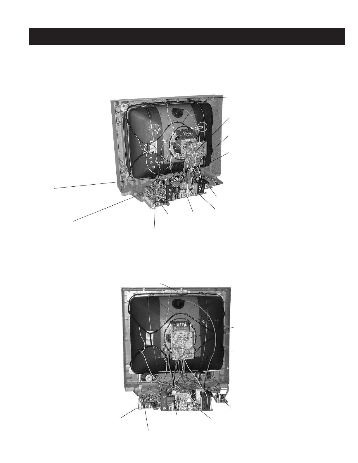
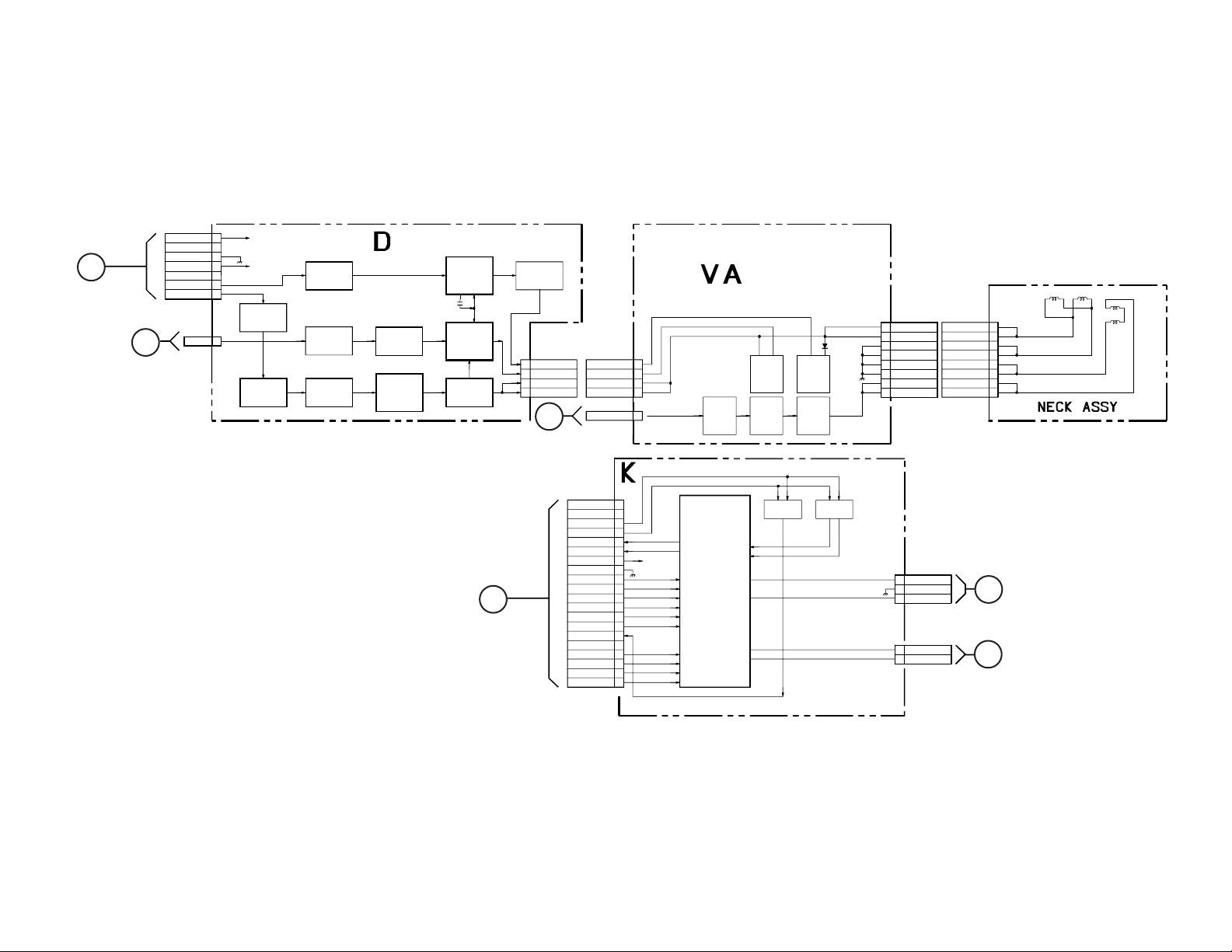
5-1. Circuit Boards Location.................................................................................................................23
5-2. Printed Wiring Board and Schematic Diagram Information .......................................................... 24
5-3. Block Diagram and Schematics ....................................................................................................25
A Board ........................................................................................................................................31
BC Board...................................................................................................................................... 36
CA Board...................................................................................................................................... 39
D Board ........................................................................................................................................41
HA Board...................................................................................................................................... 43
HB Board...................................................................................................................................... 44
HX Board...................................................................................................................................... 44
K Board ........................................................................................................................................45
MA Board .....................................................................................................................................47
P Board ........................................................................................................................................52
VA Board ...................................................................................................................................... 53
5-4. Semiconductors............................................................................................................................55
6. Exploded Views
6-1. Chassis (KV-27FV17/29FV17/29FV17C ONLY) ...........................................................................56
6-2. Picture Tube Removal (KV-27FV17/29FV17/29FV17C ONLY) .....................................................57
6-3. Chassis (KV-27FS13/27FS17 ONLY) ...........................................................................................58
6-4. Chassis (KV-32FS13/32FS17/34FS13C/34FS17 ONLY)..............................................................59
6-5. Picture Tube Removal (KV-27FS13/27FS17/32FS13/32FS17/34FS13C/34FS17 ONLY) ............ 60
7. Electrical Parts List ...................................................................................................................................... 61
X
R564 Confi rmation Method (Hold Down Confi rmation) and Readjustments...........................14
— 2 —
Page 3
KV-27FS13/ 27FS17/ 27FV17/ 29FV17/ 29FV17C/ 32FS13/ 32FS17/ 34FS13C/ 34FS17
SPECIFICATIONS
KV-27FV17/
29FV17 KV-29FV17C KV-27FS13
KV-27FS17
KV-32FS13 KV-34FS13C
KV-32FS17/
34FS17
Power requirements 120V, 60 Hz 220V, 50 Hz 120V, 60 Hz 120V, 60 Hz 120V, 60 Hz 220V, 50 Hz 120V, 60 Hz
Number of inputs/outputs
1)
Video
S Video
3)
Audio
Audio Out
, PR
Y,P
B
2)
4)
5)
3333333
2211111
3333333
1111111
1111111
Monitor Out 1 1 -- -- -- -- --
Speaker output(W) 15W x 2 15W x 2 7.5W x 2 7.5W x 2 10W x 2 10W x 2 10W x 2
Power Consumption(W)
In use(Max) 220W 210W 170W 180W 195W 195W 205W
In standby 1W 1W 1W 1W 1W 1W 1W
Dimensions(W/H/D)
(mm)
(in)
762 x 604 x 519 mm 762 x 604 x 519 mm 700 x 632 x 512 mm 762 x 604 x 519 mm 800 x 704 x 582 mm 700 x 632 x 512 mm 762 x 604 x 519 mm
7/8
30 x 23
x 20
1/2
in. 30 x 23
7/8
x 20
1/2
in. 27
5/8
x 25 x 20
1/4
in. 30 x 23
7/8
x 20
1/2
in. 31
1/2
x 27
3/4
x 23 in. 27
5/8
x 25 x 20
1/4
30 x 23
7/8
x 20
Mass
(kg) 49 kg. 49 kg. 47 kg. 49 kg. 75 kg. 75 kg. 75 kg.
(lbs) 108 lbs. 108 lbs. 103 lbs. 10 oz. 108 lbs. 163 lbs. 163 lbs. 163 lbs.
1)
Television system
American TV Standard/NTSC
Channel coverage
VHF: 2-13/ VHF: 14-69/ CATV: 1-125
1 Vp-p 75 ohms unbalanced, sync negative
2)
Y: 1 Vp-p 75 ohms unbalanced, sync negative
C: 0.286 Vp-p (Burst signal), 75 ohms
3)
500 mVrms (100% modulation), Impedance: 47 kilohms
4)
More than 408 mVrms at the maximum volume setting (variable)
More than 408 mVrms (fi x); Impedance (output): 2 kilohms
5) Y: 1.0 Vp-p, 75 ohms, sync negative; P
: Vp-p, 75 ohms
P
R
: 0.7 Vp-p, 75 ohms
B
Picture tube
Flat Trinitron® tube
1/2
in.
Visible screen size
27-inch picture measured diagonally (KV-27FS13/27FS17/27FV17/29FV17/29FV17C ONLY)
32-inch picture measured diagonally (KV-32FS13/32FS17/34FS13C/34FS17 ONLY)
Actual screen size
29-inch measured diagonally (KV-27FS13/27FS17/27FV17/29FV17/29FV17C ONLY)
34-inch measured diagonally (KV-32FS13/32FS17/34FS13C/34FS17 ONLY)
Antenna
75 ohm external terminal for VHF/UHF
Supplied Accessories
Remote Commander RM-Y180 (KV-27FS13/32FS13/34FS13C ONLY)
Remote Commander RM-Y181 (KV-27FS17/27FV17/29FV17/29FV17C/32FS17/34FS17 ONLY)
Size AA (R6) batteries (2)
Optional Accessories
Connecting cables: VMC-810S/820S, VMC-720M,
YC-15V/30V, RK74A
U/V mixer EAC-66
TV Stand: SU-27FD4 (KV-27FS13/ 27FS17/ 27FV17 ONLY)
TV Stand: SU-27FD3 (KV-29FV17/ 29FV17C ONLY)
TV Stand: SU-32FD3 (KV-34FS17/34FS13C ONLY)
TV Stand: SU-32FD4 (KV-32FS13/ 32FS17 ONLY)
Design and specifi cations are subject to change without notice.
— 3 —
(•) SRS (SOUND RETRIEVAL SYSTEM)
The (•) SRS (SOUND RETRIEVAL SYSTEM) is manufactured by
Sony Corporation under license from SRS Labs, Inc. It is covered by U.S.
Patent No. 4,748,669. Other U.S. and foreign patents pending.
The word ‘SRS’ and the SRS symbol (•) are registered trademarks of
SRS Labs, Inc. BBE and BBE symbol are trademarks of BBE Sound, Inc.
and are licensed by BBE Sound, Inc. under U.S. Patent No. 4,638,258.
Page 4

KV-27FS13/ 27FS17/ 27FV17/ 29FV17/ 29FV17C/ 32FS13/ 32FS17/ 34FS13C/ 34FS17
WARNINGS AND CAUTIONS
CAUTION
Short circuit the anode of the picture tube and the anode cap to the metal chassis, CRT shield, or carbon painted on the CRT,
after removing the anode.
WARNING!!
An isolation transformer should be used during any service to avoid possible shock hazard, because of live chassis. The chassis of
this receiver is directly connected to the AC power line.
! SAFETY-RELATED COMPONENT WARNING!!
Components identifi ed by shading and ! mark on the schematic diagrams, exploded views, and in the parts list are critical for
safe operation. Replace these components with Sony parts whose part numbers appear as shown in this manual or in supplements
published by Sony. Circuit adjustments that are critical for safe operation are identifi ed in this manual. Follow these procedures
whenever critical components are replaced or improper operation is suspected.
ATTENTION!!
Apres avoir deconnecte le cap de l’anode, court-circuiter l’anode du tube cathodique et celui de l’anode du cap au chassis metallique
de l’appareil, ou la couche de carbone peinte sur le tube cathodique ou au blindage du tube cathodique.
Afi n d’eviter tout risque d’electrocution provenant d’un chássis sous tension, un transformateur d’isolement doit etre utilisé lors de tout
dépannage. Le chássis de ce récepteur est directement raccordé à l’alimentation du secteur.
! ATTENTION AUX COMPOSANTS RELATIFS A LA SECURITE!!
Les composants identifi es par une trame et par une marque ! sur les schemas de principe, les vues explosees et les listes de
pieces sont d’une importance critique pour la securite du fonctionnement. Ne les remplacer que par des composants Sony dont
le numero de piece est indique dans le present manuel ou dans des supplements publies par Sony. Les reglages de circuit dont
l’importance est critique pour la securite du fonctionnement sont identifi es dans le present manuel. Suivre ces procedures lors de
chaque remplacement de composants critiques, ou lorsqu’un mauvais fonctionnement suspecte.
— 4 —
Page 5
KV-27FS13/ 27FS17/ 27FV17/ 29FV17/ 29FV17C/ 32FS13/ 32FS17/ 34FS13C/ 34FS17
SAFETY CHECK-OUT
After correcting the original service problem, perform the following
safety checks before releasing the set to the customer:
1. Check the area of your repair for unsoldered or poorly soldered
connections. Check the entire board surface for solder splashes and
bridges.
2. Check the interboard wiring to ensure that no wires are “pinched” or
touching high-wattage resistors.
3. Check that all control knobs, shields, covers, ground straps, and
mounting hardware have been replaced. Be absolutely certain that
you have replaced all the insulators.
4. Look for unauthorized replacement parts, particularly transistors,
that were installed during a previous repair. Point them out to the
customer and recommend their replacement.
5. Look for parts which, though functioning, show obvious signs of
deterioration. Point them out to the customer and recommend their
replacement.
6. Check the line cords for cracks and abrasion. Recommend the
replacement of any such line cord to the customer.
7. Check the B+ and HV to see if they are specifi ed values. Make sure
your instruments are accurate; be suspicious of your HV meter if sets
always have low HV.
8. Check the antenna terminals, metal trim, “metallized” knobs, screws,
and all other exposed metal parts for AC leakage. Check leakage
as described below.
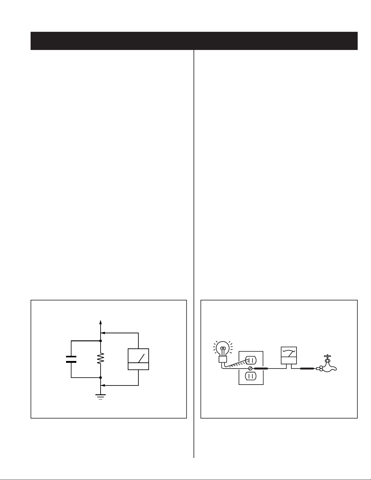
Leakage Test
The AC leakage from any exposed metal part to earth ground and from
all exposed metal parts to any exposed metal part having a return to
chassis, must not exceed 0.5 mA (500 microamperes). Leakage current
can be measured by any one of three methods.
1. A commercial leakage tester, such as the Simpson 229 or
RCA WT-540A. Follow the manufacturers’ instructions to use these
instructions.
2. A battery-operated AC milliampmeter. The Data Precision 245 digital
multimeter is suitable for this job.
3. Measuring the voltage drop across a resistor by means of a VOM
or battery-operated AC voltmeter. The “limit” indication is 0.75 V,
so analog meters must have an accurate low voltage scale. The
Simpson’s 250 and Sanwa SH-63TRD are examples of passive VOMs
that are suitable. Nearly all battery-operated digital multimeters that
have a 2 VAC range are suitable (see Figure A).
How to Find a Good Earth Ground
A cold-water pipe is a guaranteed earth ground; the cover-plate retaining
screw on most AC outlet boxes is also at earth ground. If the retaining
screw is to be used as your earth ground, verify that it is at ground
by measuring the resistance between it and a cold-water pipe with an
ohmmeter. The reading should be zero ohms.
If a cold-water pipe is not accessible, connect a 60- to 100-watt troublelight (not a neon lamp) between the hot side of the receptacle and the
retaining screw. Try both slots, if necessary, to locate the hot side on the
line; the lamp should light at normal brilliance if the screw is at ground
potential (see Figure B).
To Exposed Metal
Parts on Set
Trouble Light
Ohmmeter
0.15 F
1.5 K Ω
AC Outlet Box
AC
Voltmeter
(0.75 V)
Earth Ground
Figure A. Using an AC voltmeter to check AC leakage. Figure B. Checking for earth ground.
— 5 —
Cold-water Pipe
Page 6
KV-27FS13/ 27FS17/ 27FV17/ 29FV17/ 29FV17C/ 32FS13/ 32FS17/ 34FS13C/ 34FS17
SELF-DIAGNOSTIC FUNCTION
Self Diagnosis
Supported model
The units in this manual contain a self-diagnostic function. If an error occurs, the STANDBY/TIMER LED will automatically begin to fl ash. The number
of times the LED fl ashes translates to a probable source of the problem. A defi nition of the STANDBY/TIMER LED fl ash indicators is listed in the
instruction manual for the user’s knowledge and reference. If an error symptom cannot be reproduced, the Remote Commander can be used to review
the failure occurrence data stored in memory to reveal past problems and how often these problems occur.
Diagnostic Test Indicators
When an error occurs, the STANDBY/TIMER LED will fl ash a set number of times to indicate the possible cause of the problem. If there is more than
one error, the LED will identify the fi rst of the problem areas.
Results for all of the following diagnostic items are displayed on screen. No error has occurred if the screen displays “0”.
Diagnostic Item
Description
Power does not turn on
+B overcurrent (OCP)*
I-Prot
IK (AKB)
No. of times
STANDBY/ TIMER
lamp fl ashes
Does not light
2 times
4 times
5 times
Self-Diagnositc
Display/
Diagnostic Result
2:0 or 2:1
4:0 or 4:1
5:0 or 5:1
Probable Cause Location
• Power cord is not plugged in.
• Fuse is burned out (F601). (A Board)
• H.OUT (Q502) is shorted. (A Board)
• IC702 is shorted. (CA Board)
• +13V is not supplied. (A Board)
• IC502 is faulty. (A Board)
• Viedo OUT (IC502) is faulty. (A Board)
• IC301 is faulty. (MA Board)
• Screen (G2) is improperly adjusted.**
Detected Symptoms
• Power does not come on.
• No power is supplied to the TV.
• AC Power supply is faulty.
• Power does not come on.
• Load on power line is shorted.
• Has entered standby state after horizontal raster.
• Vertical defl ection pulse is stopped.
• Power line is shorted or power supply is stopped.
• No raster is generated.
• CRT Cathode current detection reference pulse
output is small.
*If a +B overcurrent is detected, stoppage of the vertical defl ection is detected simultaneously. The symptom that is diagnosed fi rst by the
mircrocontroller is displayed on the screen.
**Refer to Screen (G2) Adjustments in Section 2-4. of this manual.
Display of Standby/Timer LED Flash Count
2 times
4 times
5 times
LED ON 0.3 sec.
LED OFF 0.3 sec.
LED OFF
3 sec.
Standby/Timer LED
Diagnostic Item Flash Count*
+B Overcurrent 2 times
I-Prot 4 times
IK (AKB) 5 times
*One fl ash count is not used for self-diagnostic.
Stopping the Standby/Timer LED Flash
Turn off the power switch on the TV main unit or unplug the power cord from the outlet to stop the STANDBY/TIMER LAMP from fl ashing.
— 6 —
Page 7
KV-27FS13/ 27FS17/ 27FV17/ 29FV17/ 29FV17C/ 32FS13/ 32FS17/ 34FS13C/ 34FS17
Self-Diagnostic Screen Display
For errors with symptoms such as “power sometimes shuts off” or “screen sometimes goes out” that cannot be confi rmed, it is possible to bring up
past occurrences of failure on the screen for confi rmation.
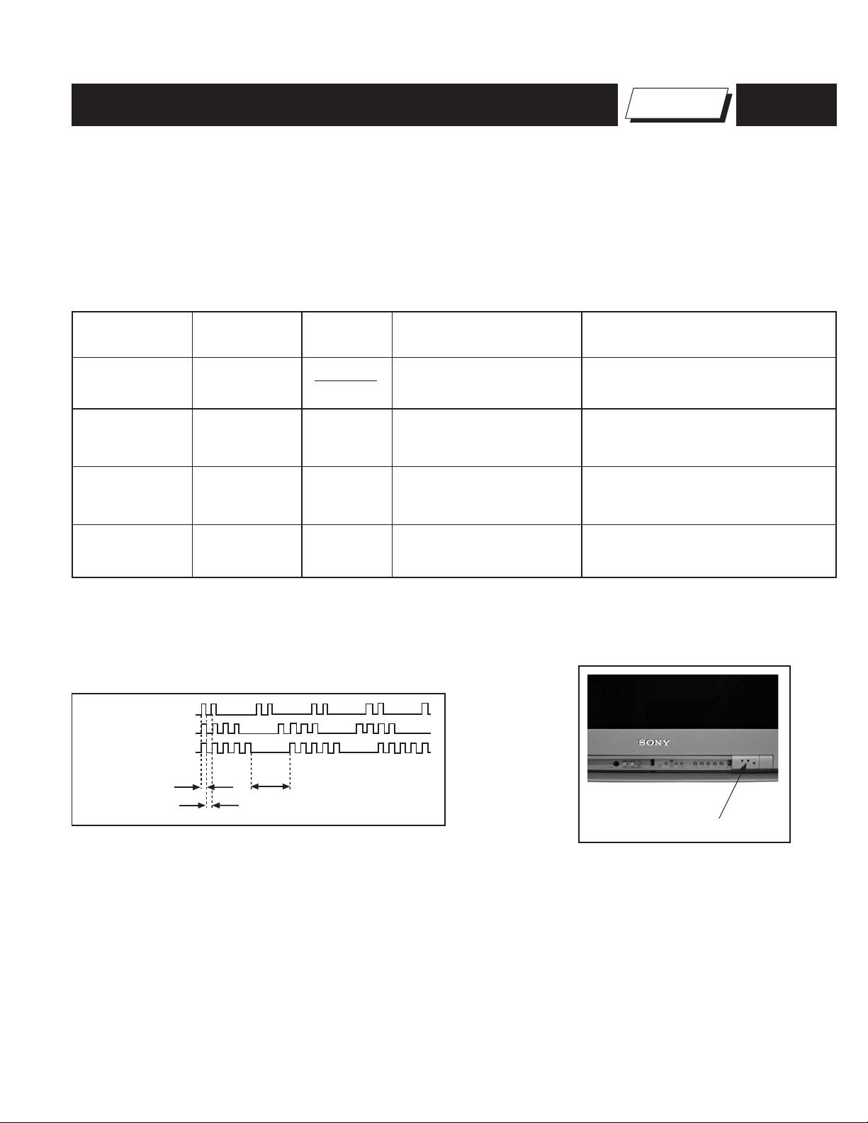
To Bring Up Screen Test
In standby mode, press buttons on the Remote Commander sequentially, in rapid succession, as shown below:
Display
Self-Diagnostic Screen Display
Handling of Self-Diagnostic Screen Display
Since the diagnostic results displayed on the screen are not automatically cleared, always check the self-diagnostic screen during repairs. When you
have completed the repairs, clear the result display to “0”.
Unless the result display is cleared to “0”, the self-diagnostic function will not be able to detect subsequent faults after completion of the repairs.
Clearing the Result Display
To clear the result display to “0”, press buttons on the Remote Commander sequentially when the diagnostic screen is displayed, as shown below:
Channel
Quitting the Self-Diagnostic Screen
To quit the entire self-diagnostic screen, turn off the power switch on the Remote Commander or the main unit.
Channel
SELF DIAGNOSTIC
2: 000
3: N/A
4: 000
5: 001
101: N/A
8
ENTER
5
Sound Volume - Power ON
Note that this differs from entering the Service Mode (Sound Volume
Numeral “0” means that no fault was detected.
Numeral “1” means a fault was detected one time only.
+
).
Self-Diagnostic Circuit
FROM
CA BOARD
IC702 PIN 5
MA BOARD
IC301
Y/CHROMA JUNGLE
36
IK IN
A BOARD
IC502
V. OUT
REF
3
MA BOARD
IC001
SYSTEM
IO-BDAT
5
I-Prot
42
MA BOARD
IC003
MEMORY
5
BDA
A BOARD
33
FROM
IC501
PIN 3
+B overcurrent (OCP)
Occurs when an overcurrent on the +B (135V) line is detected by pin 33 of IC301 (MA Board). If the voltage of pin 33 of IC301 (MA Board) is less than
1V when V.SYNC is more than seven verticals in a period, the unit will automatically turn off.
I-Prot
Occurs when an absence of the vertical defl ection pulse is detected by pin 5 of IC001 (MA Board). Power supply will shut down when waveform
interval exceeds 2 seconds.
IK (AKB)
If the RGB levels* do not balance within 2 seconds after the power is turned on, this error will be detected by IC301 (MA Board). TV will stay
on, but there will be no picture.
*(Refers to the RGB levels of the AKB detection Ref pulse that detects 1K).
HP/PROTECT
SDA
61
43
IO-SDAT
O-LED
22
DISPLAY
— 7 —
Page 8
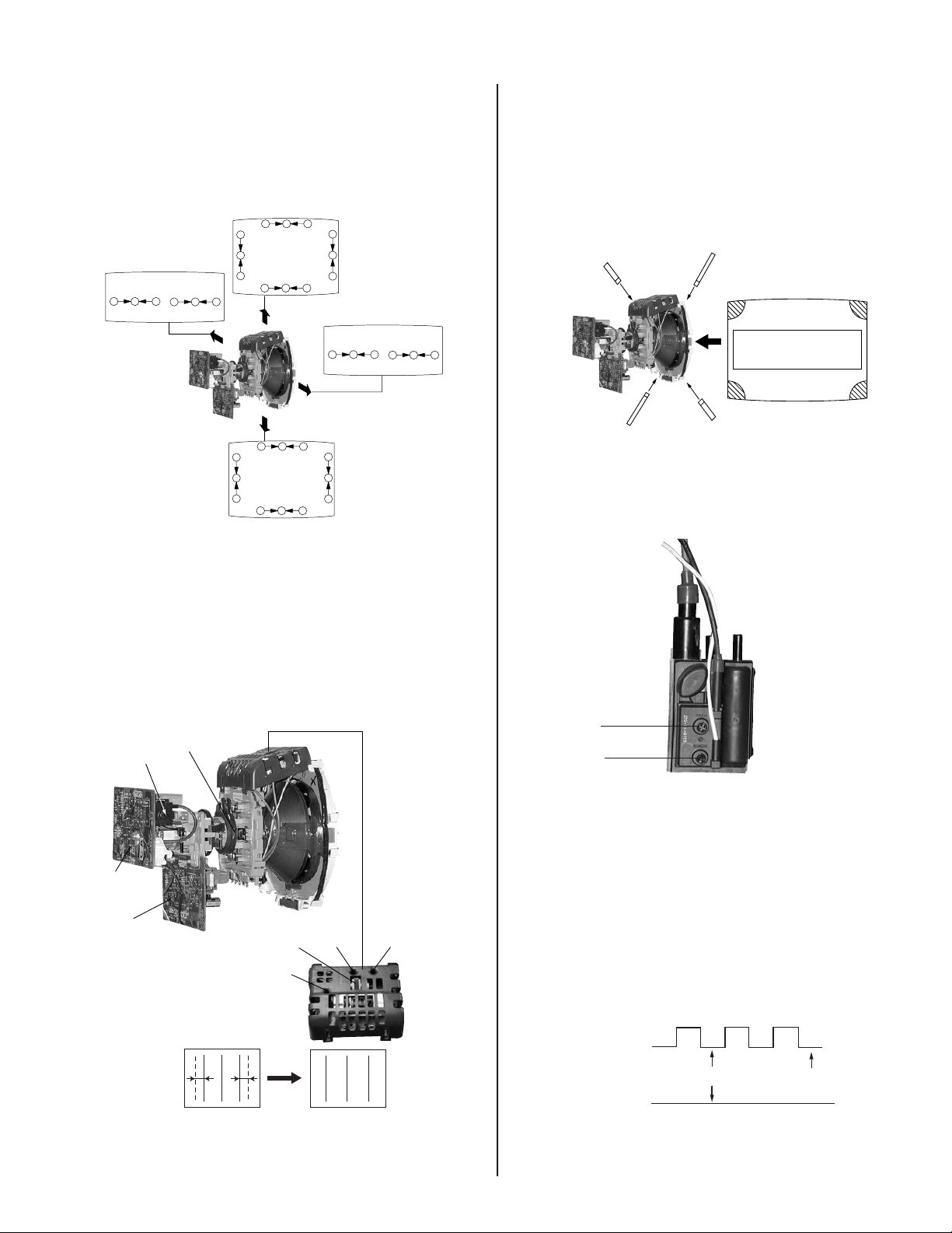
1-1. REAR COVER REMOVAL
KV-27FS13/ 27FS17/ 27FV17/ 29FV17/ 29FV17C/ 32FS13/ 32FS17/ 34FS13C/ 34FS17
SECTION 1: DISASSEMBLY
KV-27FS13/27FS17/27FV17/29FV17/29FV17C
3 Screws (+BVTP 4x16)
4 Screws
(+BVTP 4x16)
2 Screws
(+BVTP 3x12)
Rear Cover
3 Screws
(+BVTP 4x16)
2 Screws
(+BVTP 4x16)
1-2. CHASSIS ASSEMBLY REMOVAL
KV-32FS13/32FS17/34FS13C/34FS17 ONLY
3 Screws (+BVTP 4x16)
5 Screws
(+BVTP 4x16)
2 Screws
(+BVTP 3x12)
Rear Cover
1-3. SERVICE POSITION
6 Screws
(+BVTP 4x16)
Claw
Chassis Assembly
— 8 —
CA Board
VA Board
D Board
A Board
MA Board
Page 9
KV-27FS13/ 27FS17/ 27FV17/ 29FV17/ 29FV17C/ 32FS13/ 32FS17/ 34FS13C/ 34FS17
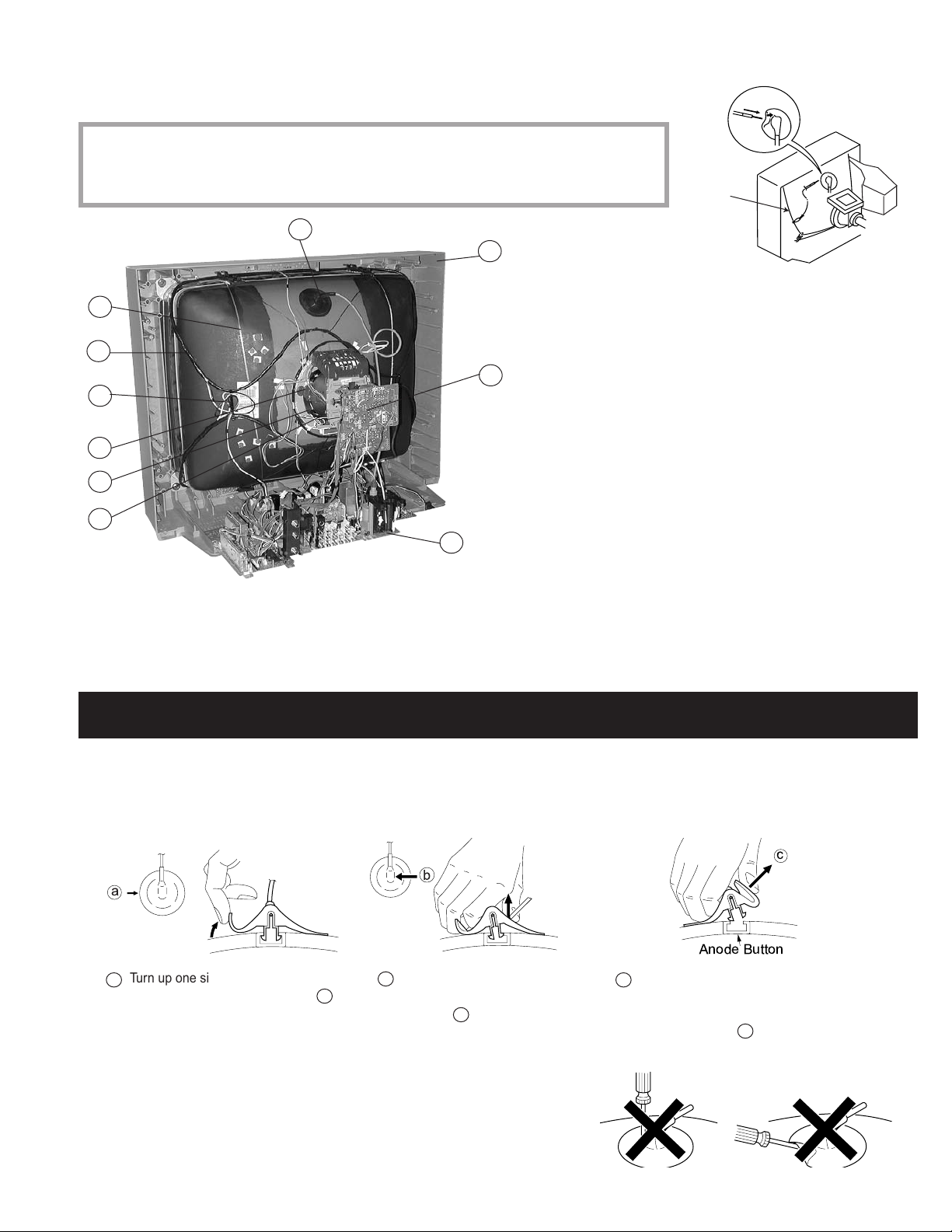
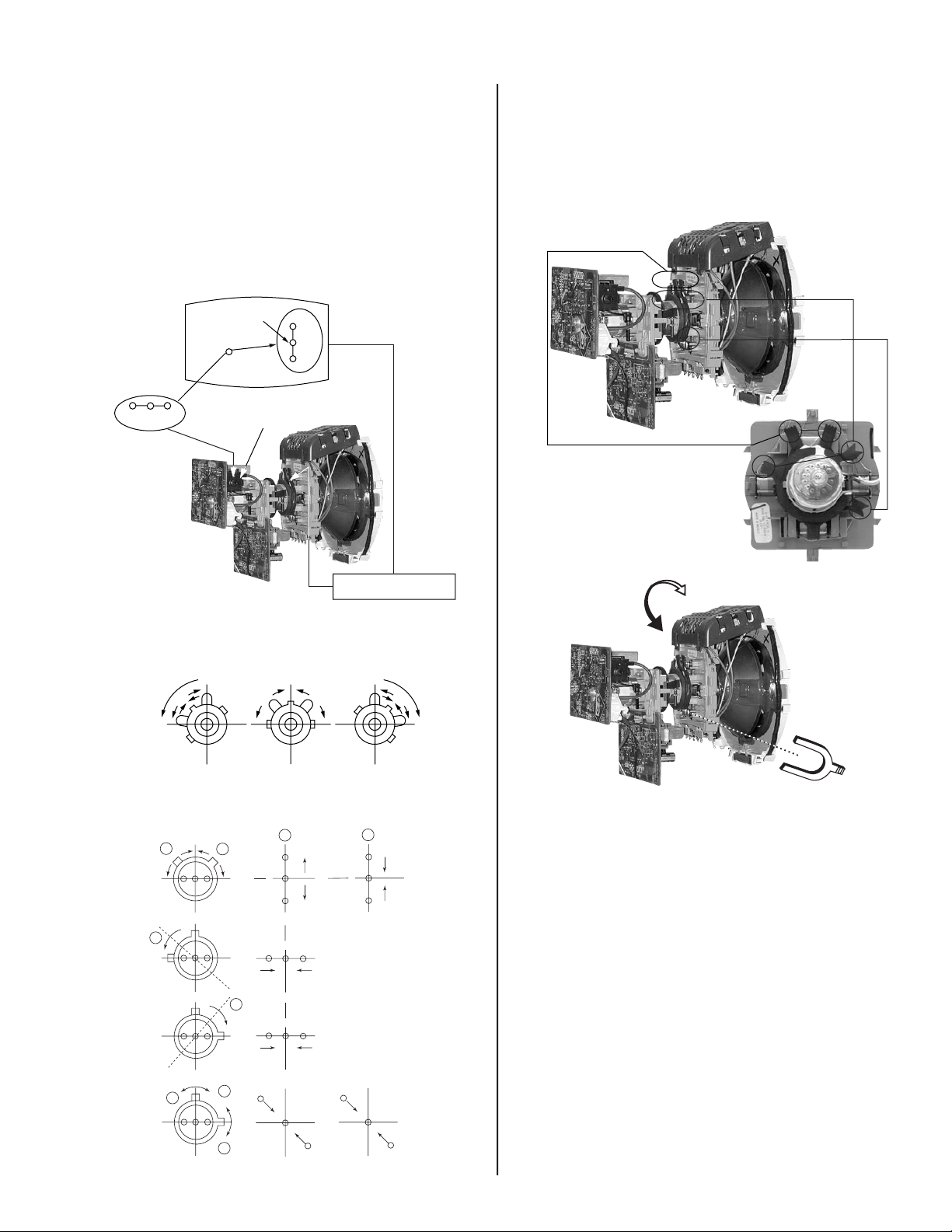
1-4. PICTURE TUBE REMOVAL
WARNING: BEFORE REMOVING THE ANODE CAP
High voltage remains in the CRT even after the power is disconnected. To avoid electric shock,
discharge CRT before attempting to remove the anode cap. Short between anode and CRT
coated earth ground strap.
1
10
Coated
Earth
Ground
Strap
9
8
3
7
6
2
5
4
1. Discharge the anode of the CRT and remove the anode cap.
2. Unplug all interconnecting leads from the defl ection yoke, neck
assembly, degaussing coils and CRT grounding strap.
3. Remove the CA and VA Board from the CRT.
4. Remove the chassis assembly.
5. Loosen the neck assembly fi xing screw and remove.
6. Loosen the defl ection yoke fi xing screw and remove.
7. Place the set with the CRT face down on a cushion and remove
the degaussing coil holders.
8. Remove the degaussing coils.
9. Remove the CRT grounding strap and spring tension devices.
10. Unscrew the four CRT fi xing screws [located on each CRT
corner] and remove the CRT [Take care not to handle the CRT
by the neck].
ANODE CAP REMOVAL PROCEDURE
WARNING: High voltage remains in the CRT even after the power is disconnected. To avoid electric shock, discharge CRT before attempting to remove
the anode cap. Short between anode and coated earth ground strap of CRT.
NOTE: After removing the anode cap, short circuit the anode of the picture tube and the anode cap to either the metal chassis, CRT shield, or
carbon painted on the CRT.
c
b
a
Anode Button
Turn up one side of the rubber cap
1
inthe direction indicated by arrow
a
.
Use your thumb to pull the rubber
2
cap fi rmly in the direction indicated
by arrow
.
b
HOW TO HANDLE AN ANODE CAP
1. Do not use sharp objects which may cause damage to the surface of the anode
cap.
2. To avoid damaging the anode cap, do not squeeze the rubber covering too hard.
A material fi tting called a shatter-hook terminal is built into the rubber.
3. Do not force turn the foot of the rubber cover. This may cause the shatter-hook
terminal to protrude and damage the rubber.
When one side of the rubber cap separates from
3
the anode button, the anode cap can be removed
by turning the rubber cap and pulling it in the
direction of arrow
.
c
— 9 —
Page 10
KV-27FS13/ 27FS17/ 27FV17/ 29FV17/ 29FV17C/ 32FS13/ 32FS17/ 34FS13C/ 34FS17
SECTION 2: SET-UP ADJUSTMENTS
The following adjustments should be made when a complete
realignment is required or a new picture tube is installed.
These adjustments should be performed with rated power supply
voltage unless otherwise noted.
Set the controls as follows unless otherwise noted:
VIDEO MODE: Standard
PICTURE CONTROL: Normal
BRIGHTNESS CONTROL: Normal
2-1. BEAM LANDING
Before beginning adjustment procedure:
1. Degauss the entire screen.
2. Feed in the white pattern signal.
ADJUSTMENT PROCEDURE
1. Input a raster signal with the pattern generator.
2. Loosen the defl ection yoke mounting screw, and set the purity control
to the center as shown below:
Purity Control
Perform the adjustments in order as follows:
1. Beam Landing
2. Convergence
3. Focus
4. Screen (G2)
5. White Balance
Note Test Equipment Required:
1. Color Bar Pattern Generator
2. Degausser
3. DC Power Supply
4. Digital Multimeter
6. Switch over the raster signal to red and blue and confi rm the
condition.
7. When the position of the defl ection yoke is determined, tighten it with
the defl ection yoke mounting screw.
8. If landing at the corner is not right, adjust by using the disk magnets.
3. Turn the raster signal of the pattern generator to green.
4. Move the defl ection yoke backward, and adjust with the purity control
so that green is in the center and red and blue are even on both
sides.
Blue Red
Green
5. Move the defl ection yoke forward, and adjust so that the entire screen
becomes green.
— 10 —
Purity control
corrects this area.
Disk magnets
or rotatable disk
magnets correct
these areas. (a-d)
Deflection yoke positioning
b
d
a
b
cd
corrects these areas.
a
c
Page 11
KV-27FS13/ 27FS17/ 27FV17/ 29FV17/ 29FV17C/ 32FS13/ 32FS17/ 34FS13C/ 34FS17
2-2. CONVERGENGE
Before starting convergence adjustments:
1 Perform FOCUS, VLIN and VSIZE adjustments.
2. Set BRIGHTNESS control to minimum.
3. Feed in dot pattern.
VERTICAL STATIC CONVERGENCE
1. Adjust V. STAT magnet to converge red, green and blue dots in the
center of the screen (Vertical movement adjusts V.STAT RV701 to
converge).
Center dot
RV701
R
B
G
V.STAT
R
G
B
HORIZONTAL STATIC CONVERGENCE
If the blue dot does not converge with the red and green dots, peform
the following:
1. Move BMC magnet (a) to correct insuffi cient H.Static convergence.
2. Rotate BMC magnet (b) to correct insuffi cient V.Static convergence.
3. After adjusting the BMC magnet, repeat Beam Landing Adjustment.
V.S TAT
BMC MAGNET
PURITY
V.STAT magnet
2. Tilt the V. STAT magnet and adjust static convergence to open or close
the V. STAT magnet.
When the V. STAT magnet is moved in the direction of arrow a and b,
red, green, and blue dots move as shown below:
(1)
a
b
(2)
a
b
b
a
B
G
R
BGR
RGB
b
B
G
R
b
BMC magnet
a
(3)
b
a
R
G
b
B
G
B
R
— 11 —
Page 12
KV-27FS13/ 27FS17/ 27FV17/ 29FV17/ 29FV17C/ 32FS13/ 32FS17/ 34FS13C/ 34FS17
DYNAMIC CONVERGENCE ADJUSTMENT
Before performing this adjustment, perform Horizontal and Vertical Static
Convergence Adjustment.
1. Slightly loosen defl ection yoke screw.
2. Remove defl ection yoke spacers.
3. Move the defl ection yoke for best convergence as
shown below:
G
B
R
R
G
B
BGR
B
G
R
R
R
B
G
R
B
B
G
R
B
G
BGR
B
G
R
G
B
R
G
R
GB
4. Adjust XCV core to balance X axis.
5. Adjust YCH VR to balance Y axis.
6. Adjust vertical red and blue convergence with V.TILT (TLV VR).
Note: Perform adjustment 3-6 while tracking items 1 and 2.
SCREEN-CORNER CONVERGENCE
1. Affi x a permalloy assembly corresponding to the misconverged areas:
b
a
ba
a-d: screen-corner
misconvergence
c
d
c
d
2-3. FOCUS
1. Adjust FOCUS control for best pictures.
4. Tighten the defl ection yoke screw.
5. Install the defl ection yoke spacers.
TLH PLATE ADJUSTMENT
1. Input crosshatch pattern.
2. Adjust PICTURE QUALITY to standard, PICTURE and BRIGHTNESS
to 50%, and OTHER to standard.
3 Adjust the Horizontal Convergence of red and blue dots by tilting the
TLH plate on the defl ection yoke.
RV701
V. S TAT
CA
Board
VA
Board
TLH Plate
XCV
(TLV)
YCH
TLV
Focus (FV)
Screen (G2)
2-4. SCREEN (G2)
1. Input a dot pattern.
2. Set the PICTURE and BRIGHTNESS controls at minimum and
COLOR control at normal.
3. Adjust SBRT, GCUT, BCUT in service mode with an oscilloscope as
shown below so that voltages on the red, green, and blue cathodes
are 170 ± 2VDC.
B R R B
(R)(B) (B)(R)
TLH+
TLH-
— 12 —
Ground
170 ± 2 VDC
Pedestal
Page 13
2-5. METHOD OF SETTING THE SERVICE
ADJUSTMENT MODE
SERVICE MODE PROCEDURE
1. Standby mode (power off).
2. Press
Display
Channel 5 Sound Volume + Power
on the Remote Commander (press each button within a second).
SERVICE ADJUSTMENT MODE ON
1. The CRT displays the time being adjusted.
KV-27FS13/ 27FS17/ 27FV17/ 29FV17/ 29FV17C/ 32FS13/ 32FS17/ 34FS13C/ 34FS17
2. Press
3. Press
4. Press
Display
hsiz 16
to save into the memory.
service
ntsc
vchp
then
Category
defl
00000000
ENTER
Mode
Signal
Type
1
or 4 on the Remote Commander to select the time.
3
or 6 on the Remote Commander to change the data.
MUTING
Item
00000000
Display
Item
SERVICE ADJUSTMENT MODE MEMORY
Turn the set off then on to exit Service Adjustment Mode.
Signal
Type
Category
Mode
service defl hsiz 16
ntsc
vchp 00000000 00000000
Display
Item
write
Item
Data
MUTING
ENTER
Green
Red
2-6. WHITE BALANCE ADJUSTMENTS
1. Input an entire white signal with burst.
2. Set to Service Adjustment Mode.
3. Set the PICTURE and BRIGHTNESS to minimum.
4. Adjust with SBRT if necessary.
5. Select GCUT and BCUT with
6. Adjust with
3
and 6 for the best white balance.
7. Set the PICTURE and BRIGHTNESS to maximum.
8. Select GDRV and BDRV with
9. Adjust with
3
and 6 for the best white balance.
10. To write into memory, press
1
and 4 .
1
and 4.
MUTING
then
ENTER
.
— 13 —
Page 14
KV-27FS13/ 27FS17/ 27FV17/ 29FV17/ 29FV17C/ 32FS13/ 32FS17/ 34FS13C/ 34FS17
SECTION 3: SAFETY RELATED ADJUSTMENTS
3-1. X R564 CONFIRMATION METHOD
(HOLD-DOWN CONFIRMATION) AND
READJUSTMENTS
The following adjustments should always be performed when replacing
the following components which are marked with
diagram:
Part Replaced ( )
DY, T505, CRT, IC501 C507,
C520, C505, C509, C515, T504,
Y
on the schematic
Adjustment ( )
HV HOLD-DOWN
R564
T503, C551, L510, C546, C537,
C547, D517, D518, D519, R560,
R561, R562, R563, R565, R566,
R567, R525....................A Board
IC301........................MA Board
PREPARATION BEFORE CONFIRMATION
1. Using a Variac, apply AC input voltage: 120 ±2 VAC.
2. Turn the POWER switch ON.
3. Input a white signal and set the PICTURE and BRIGHTNESS controls
to maximum.
4. Confi rm that the voltage between C546 (+) or TP503 and ground is
more than 21.0 VDC (27/29 inch) or 23.0 VDC (32/34 inch).
HOLD-DOWN OPERATION CONFIRMATION
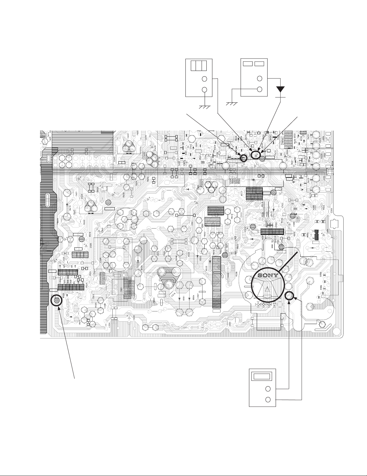
1. Connect the current meter between Pin 11 of the FBT (T505) and
the PWB land where Pin 11 would normally attach (See Figure 1 on
the next page).
2. Input a dot signal and set PICTURE and BRIGHTNESS to minimum:
IABL = 1730 ± 100µA. (27/29 inch) or 2175 +100 - 325µA (32/34inch).
3. Confi rm the voltage of A Board TP-600 is 135 ± 1.5 VDC.
4. Connect the digital voltmeter and the DC power supply via Diode
1SS119 to C546 (+) and ground (See Figure 1 on next page).
5. Increase the DC power voltage gradually until the picture blanks out.
6. Turn DC power source off immediately.
7. Read the digital voltmeter indication (standard 24.78 +0/ -0.1 VDC
[27/29 inch] or 27.24 +0/-0.1 VDC [32/34 inch]).
8. Input a white signal and set PICTURE and BRIGHTNESS to
maximum: IABL = 1730 ± 100µA (27/29 inch) or 2175 +100/-325 µA
(32/34 inch).
9. Repeat steps 4 to 7.
HOLD-DOWN READJUSTMENT
If the setting indicated in Step 2 of Hold-Down Operation Confi rmation
cannot be met, readjustment should be performed by altering the
resistance value of R564 component marked with
X
.
T505
FBT
ampmeter
3.0 mA DC
range
ABL
+
-
A
IABL
3-2. B+ VOLTAGE CONFIRMATION AND
ADJUSTMENT
Note: The following adjustments should always be performed when
replacing the following components, which are marked with
schematic diagram on the A Board:
A BOARD: IC601, PH601
1. Using a Variac, apply AC input voltage: 130 + 2.0/ -0.0 VAC
2. Input a monoscope pattern.
3. Set the PICTURE and the BRIGHTNESS controls to minimum.
4. Confi rm the voltage of A Board TP-600 is <136.5 VDC.
5. If step 4 is not satisfi ed, replace the components listed above, then
repeat Steps 1 – 3.
Y
on the
— 14 —
Page 15
KV-27FS13/ 27FS17/ 27FV17/ 29FV17/ 29FV17C/ 32FS13/ 32FS17/ 34FS13C/ 34FS17
11119
+
+
+
+
18
1818
6
5
9
C
6
5
9
C
6
5
9
C
6
5
9
C
R601
R601
R601R601
R615
R615
R615R615
D616
D616
D616D616
B
6
1
F
0
B
6
1
F
0
B
6
1
F
0
B
6
1
F
0
C624
C624
C624C624
H.DRIVE
H.DRIVE
H.DRIVEH.DRIVE
CN511
C611
C611
C611C611
C654
C654
C654C654
CN506
CN506
CN506CN506
1111
1111
CN515
CN515
CN515CN515
+B
+B
+B+B
R515
R515
R515R515
CN511
CN511CN511
1111
R516
R516
R516R516
C536
C536
C536C536
D521
D521
D521D521
C554
C554
C554C554
4444
5555
7777
R503
R503
R503R503
C503
C503
C503C503
R502
R502
R502R502
R547
R547
R547R547
9
99
10
1018
1010
R
6
5
R
6
5
9
9
R
6
5
R
6
5
9
9
T503
T503
T503T503
L602
L602
L602L602
C629
C629
C629C629
H.PULSE
H.PULSE
H.PULSEH.PULSE
FB503
FB503
FB503FB503
R507
R507
R507R507
T502
T502
T502T502
Q501
Q501
Q501Q501
C504
C504
C504C504
4444
R518
R518
R518R518
C530
C530
C530C530
R529
R529
R529R529
5555
R531
R531
R531R531
6666
R539
R539
R539R539
C543
C543
C543C543
V DY -
V DY -
V DY -V DY -
V DY +
V DY +
V DY +V DY +
H DY -
H DY -
H DY -H DY H DY -
H DY -
H DY -H DY -
H DY +
H DY +
H DY +H DY +
H DY +
H DY +
H DY +H DY +
R545
R545
R545R545
POWER
SUPPLY
R438
R438
R438R438
R563
R563
R563R563
C546
C546
C546C546
R573
R573
R573R573
C541
C541
C541C541
D510
D510
D510D510
6
6
6
6
6
6
6
6
7
7
7
7
R540
R540
R540R540
C519
C519
C519C519
R537
R537
R537R537
TH501
TH501
TH501TH501
200V
200V
200V200V
D511
D511
D511D511
C552
C552
C552C552
L507
L507
L507L507
+
1SS119
C546
R225
R225
R403
R403
R403R403
H.PROT
H.PROT
H.PROTH.PROT
C542
C542
C542C542
2
2
2
2
4
4
4
4
2
2
2
2
C518
C518
C518C518
IC502
IC502
IC502IC502
1
1
1
1
R543
R543
R543R543
6
6
6
6
R225R225
D235
D235
D235D235
D234
D234
D234D234
C213
C213
C213C213
R218
R218
R218R218
R407
R407
R407R407
-13V
-13V
-13V-13V
HEATER
HEATER
HEATERHEATER
C211
C211
C211C211
Q205
Q205
Q205Q205
Q206
Q206
Q206Q206
D232
D232
D232D232
C523
C523
C523C523
R532
R532
R532R532
1
1
1
1
CN502
CN502
CN502CN502
Q201
Q201
Q201Q201
D236
D236
D236D236
R231
R231R232
R232
R231R231
R232R232
D233
D233
D233D233
R511
R511
R511R511
D518
D518
D518D518
D517
D517
R561
R561
D517D517
R561R561
D514
D514
D514D514
C532
C532
C532C532
JR502
JR502
JR502JR502
T505 FBT
135V
135V
135V135V
T505
T505
T505T505
R226
R226
R226R226
R227
R227
R227R227
D520
D520
D520D520
R558
R558
R558R558
R559
R559
R559R559
R557
R557
R557R557
Q505
Q505
Q505Q505
R554
R554
R554R554
D516
D516
D516D516
R555
R555
R555R555
R535
R535
R535R535
JUMPER-ID
JUMPER-ID
JUMPER-IDJUMPER-ID
R801
R801
R801R801
R803
R803
R803R803
R804
R804
R804R804
CN504
CN504
CN504CN504
DIGITAL
MULTIMETER
+
-
X
R564
R449
R449
R454
R454
R454R454
JR503
JR503
JR503JR503
R445
R445
R445R445
Q411
Q411
Q411Q411
D620
D620
D620D620
R506
R506
C510
C510
C510C510
T504
T504
T504T504
L509
L509
L509L509
C513
C513
C513C513
R505
R505
R505R505
C555
C555
C555C555
R504
R504
R504R504
R553
R553
R553R553
R506R506
L502
L502
L502L502
L505
L505
L505L505
C517
C517
C517C517
E
E
E
E
C
C
C
C
0
2
Q
5
0
2
Q
5
0
2
Q
5
0
2
Q
5
O
H
-
O
H
-
U
T
U
T
O
H
-
O
H
-
U
T
U
T
C505
C505
C505C505
C509
C509
C509C509
C515
C515
C515C515
L510
L510
L510L510
D507
D507
D507D507
C524
C524
C524C524
D506
D506
D506D506
C550
C550
C550C550
C511
C511
C511C511
L501
L501
L501L501
B
B
B
B
B
B
B
B
R568
R568
R568R568
R449R449
C448
C448
C448C448
R450
R450
R450R450
R567
R567
R567R567
R565
R565
R565R565
R525
R525
R525R525
Q503
Q503
Q503Q503
R447
R447
R447R447
R541
R541
R541R541
R514
R514
R514R514
FB502
FB502
FB502FB502
IC501
IC501
IC501IC501
R522
R522
R522R522
8888
R527
R527
1111
R527R527
B
B
B
E
B
E
E
E
E
E
E
E
C525
C525
C525C525
5555
4444
3333
2222
1111
C
N
5
0
1
C
N
5
0
1
C
N
5
0
1
C
N
5
0
1
R546
R546
R546R546
R533
R533
R533R533
R534
R534
C551
C551
R534R534
C551C551
TP600
AMMETER
3mA dc range
A
+
-
Figure 1
— 15 —
Page 16
KV-27FS13/ 27FS17/ 27FV17/ 29FV17/ 29FV17C/ 32FS13/ 32FS17/ 34FS13C/ 34FS17
j
SECTION 4: CIRCUIT ADJUSTMENTS
ELECTRICAL ADJUSTMENTS BY REMOTE COMMANDER
Use the Remote Commander (RM-Y180, RM-Y181) to perform the circuit adjustments in this section.
Test Equipment Required: 1. Pattern generator 2. Frequency counter 3. Digital multimeter 4. Audio oscillator
4-1. SETTING THE SERVICE ADJUSTMENT
MODE
1. Standby mode (Power off).
2. Press the following buttons on the remote commander within a
second of each other:
Display
Channel 5 Sound Volumne + Power
SERVICE ADJUSTMENT MODE ON
1. The CRT displays the item being adjusted.
2. Press
3. Press
4. Press
Category
Mode
service defl hsiz 16
Signal
Type
1
or 4 on the Remote Commander to select the item.
3
or 6 on the Remote Commander to change the data.
MUTING
ntsc
vchp 00000000 00000000
then
ENTER
Display
to write into memory.
Item
Item
Data
SERVICE ADJUSTMENT MODE MEMORY
Signal
Type
1. Press
Category
Mode
service defl hsiz 16
ntsc
vchp 00000000 00000000
8
ENTER
Mode
then
Category
on the Remote Commander to initialize.
Display
Item
Display
Item
write
Item
Data
Item
Data
MUTING
ENTER
Green
Red
4-2. MEMORY WRITE CONFIRMATION
METHOD
1. After adjustment, pull out the plug from the AC outlet, then replace
the plug in the AC outlet again.
2. Turn the power switch ON and set to Service Mode.
3. Call the adjusted items again to confi rm they were adjusted.
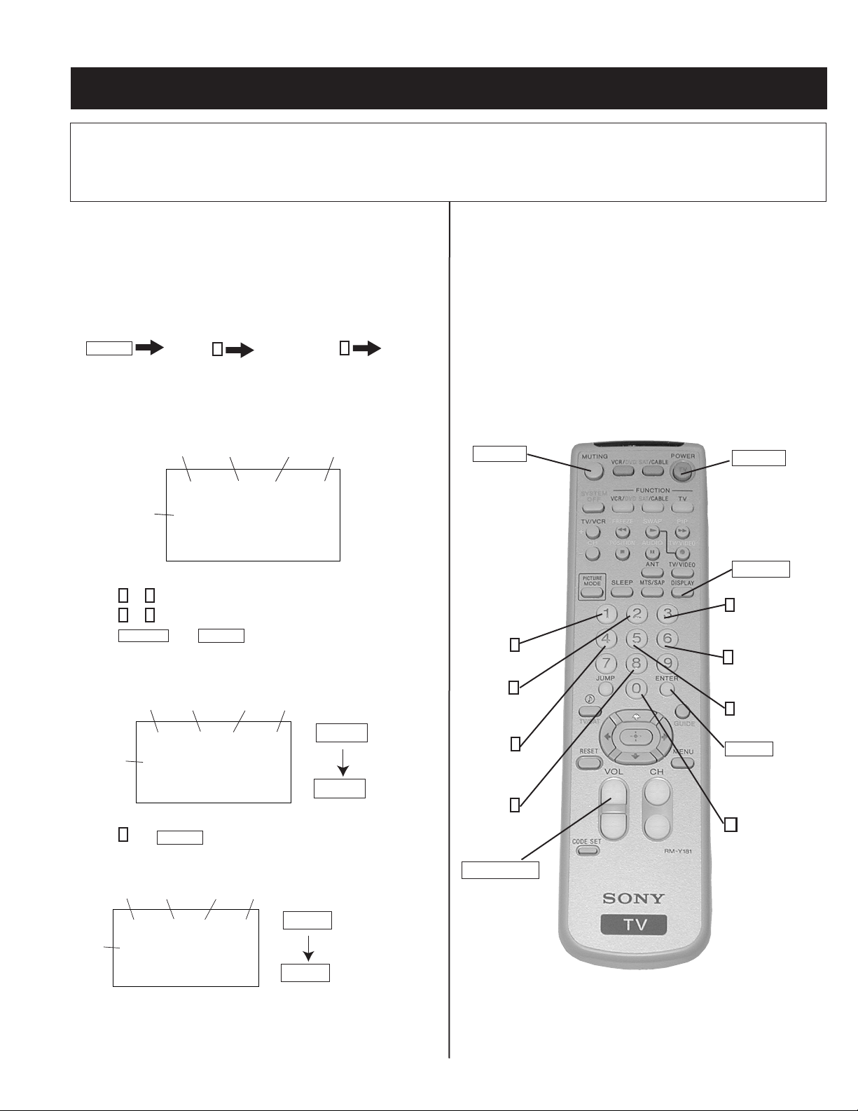
4-3. REMOTE ADJUSTMENT BUTTONS AND
INDICATORS
MUTING
(Enter into
memory)
1
Disp. (Item up)
2
(Device Item Up)
4
Disp. (Item down)
8
(Initialize)
VOLUME (+)
(Service Mode)
POWER
(Service Mode)
DISPLAY
(Service Mode)
3
Item (Data up)
6
Item (Data down)
5
(Device item down)
ENTER
(Enter into
memory)
0
(Remove from
memory)
MUTING
ENTER
Carry out Step 1 when adjusting
IDs 0-6 and when replacing and
ad
usting IC003
Signal
Type
service defl hsiz 16
ntsc
vchp 00000000 00000000
write
2. Turn set off then on to exit service adjustment mode.
Green
Red
RM-Y181
— 16 —
Page 17
KV-27FS13/ 27FS17/ 27FV17/ 29FV17/ 29FV17C/ 32FS13/ 32FS17/ 34FS13C/ 34FS17
ADJUSTMENT ITEMS (1 OF 4)
FIX
NTSC
Reg # ITEM FUNCTION RANGE
1 HSIZ Horizontal Size Adjustment 0-63 0 18 11 22
2 HPOS Horizontal Position Adjustment 0-63 13 13 20 22
3 VBOW Vertical Line Bowing Adj. 0-15 9 9 7 9
4 VANG Vertical Line Bowing Slant Adj. 0-15 8 3 9 7
5 VTRP TRAPEZIUM 0-31 19 18 21 17
6 HTRP Horiz. Trapezoid 0-15 6 6 0 2
7 TROT Tilt Correction 0-63 31 31 31 31
8 PAMP Horizontal PIN distortion Adj. 0-63 19 27 20 27
9 UPIN Upper PIN Distortion Adj. 0-63 34 41 37 38
10 LPIN Lower PIN Distortion Adj. 0-63 32 39 33 35
11 VSIZ Vertical Size Adjustment 0-63 32 51 33 51
12 VPOS Vertical Position Adj. 0-63 30 42 36 39
13 VLIN Vertical Lineality Adj. 0-15 3 5 3 4
14 SCOR Vertical "S" Correction Adjustment 0-15 6 8 8 8
15 VZOM 16:9 CRT Z Mode on/off 0-1 0 0 0
16 EHT Vertical High-Voltage Compensation 0-15 5 5 5
17 ASP Aspect Ratio Control 0-63 47 47 47
18 SCRL 16:9 CRT Z Mode Trans. Scroll 0-63 31 31 31
19 HBLK Horizontal Blanking on/off 0-1 1 1 1
20 LBLK Left Blanking Adjustment 0-15 **** 13 13
21 RBLK Rigth Blanking Adjustment 0-15 ***** 7 8
22 HDW Horizontal Drive Pulse Width 0-1 1 1 1
23 EWDC "Parabola" EW, D.C. Adjustment 0-1 0 0 0
24 LVLN Lower Screen BTM Vertical Line Adj. 0-15 0 0 0
25 UVLN Uppe Screen BTM Vertical Line Adj. 0-15 0 0 0
26 INTL INTERLACE 0-3 0 0 0
27 G2SW 0-1 0 0 0
28 G2LV 0-7 0 0 0
29 HOSC Horizontal VCO Oscillation Freq. 0-15 12 7 7
30 VSS Vertical Sync Slice Level 0-3 0 0 0
31 HSS Horizontal Sync Slice Level 0-1 0 0 0
32 HMSK For Macro Vision 0-1 0 0 0
33 VTMS Select Signal VTIM Pin 0-3 0 0 0
34 CDMD Vertical Count Down Mode Switching 0-3 3 * 3 3
35 AFC AFC Loop Gain Switching 0-3 0 0 0
36 FIFR Field Frequency 0-3 3 3 3
37 VBLK VBLKW 0-3 0 0 0
38 REFP REFP 0-1 0 0 0
39 JPSW JUMPSW 0-1 MENU 0 0
40 RDRV R Output Drive control 0-63 *** 31 40
41 GDRV G Output Drive control 0-63 25 22 42
42 BDRV B Output Drive control 0-63 25 21 31
43 RCUT R Output Cutoff control 0-63 31 31 31
44 GCUT G Output Cutoff control 0-63 15 13 12
45 BCUT B Output Cutoff control 0-63 12 14 15
46 SCON SUB CONT 0-15 8 11 11
47 SHUE Sub HUE adjustment 0-15 16 17 16
48 SCOL Sub COLOR adjustment 0-15 18 17 18
49 SBRT Sub BRIGHTNESS adjustment 0-31 16 15 16
50 CHUE SUB COLOR (RF) 0-31 7 6 6
51 CCOL SUB COLOR (RF) 0-31 7 7 4
52 UOFS YUV U OFFSET 0-15 7 7 7
53 VOFS YUV V OFFSET 0-15 7 7 7
54 RON R Output on/off 0-1 1 1 1
* CDMD = 3 for US & CND, CDMD = 0 for Other
*** RDRV = 41 for 27FS/32FS families, 31 for 27FV family
****LBLK = 0 for 27FV/29FV/32FS/34FS family, 5 FOR 27FS family
***** RBLK = 3 for 27FV/29FV/32FS/34FS family, 2 for 27FS family
DATA
27 VIDEO
— 17 —
NTSC
32 RF
AVERAGE
DATA 27
AVERAGE
DATA 32
Page 18
ADJUSTMENT ITEMS (2 OF 4)
KV-27FS13/ 27FS17/ 27FV17/ 29FV17/ 29FV17C/ 32FS13/ 32FS17/ 34FS13C/ 34FS17
FIX
Reg # ITEM FUNCTION RANGE
55 GON G Output on/off 0-1 1 1 1
56 BON B Output on/off 0-1 1 1 1
57 AXPL Axis PAL 0-1 0 0 0
58 AXNT Axis NTSC 0-1 1 1 1
59 CBPF Chroma BPF on/off 0-1 1 1 1
60 CTRP Y TRAP FILTER on/off 0-1 1 1 1
61 COFF Color On/off 0-1 0 0 0
62 KOFF Set Color Killer 0-1 0 0 0
63 SSHP Sub SHARPNESS 0-15 5 5 5
64 SHPF SHARPNESS Circuit Fo 0-3 Palette Mode Controls This Register 2 2
65 PREL Pre-Shoot/ Over-Shoot 0-1 1 0 0
66 Y-DC DC transmission Ratio Switching 0-3 Palette Mode Controls This Register 2 2
67 GAMM Gamma Correction 0-3 Palette Mode Controls This Register 2 2
68 ABLM ABL Mode Switch 0-1 1 1 1
69 VTH ABL CD VHT Switching 0-1 1 1 1
70 YDEL Y Delay Time Control 0-15 7 7 7
71 NCOL No Color ID 0-1 1 1 1
72 FSC FSC Out on/off 0-1 1 1 1
73 K-ID Killer ID Control on/off 0-1 0 0 0
74 GDOF 0-31 3 3 3
75 BDOF 0-31 16 16 16
76 GCOF 0-31 16 16 16
77 BCOF 0-31 7 7 7
78 SYSC Color System 0-7 4 4 4
79 VENH Vertical Enhancement 0-7 Palette Mode Controls This Register 5 3
80 PDSO PDS OFF 0-1 0 0 0
81 CK CK 0-1 0 0 0
82 VNL VNL 0-15 3 3 3
83 HPK HPK 0-1 0 0 0
84 HPKO HPK OFF 0-1 Palette Mode Controls This Register 0 0
85 CORE CORE 0-3 2 1 1
86 TRAP TRAP 0-1 1 1 1
87 CHTR CH TRAP 0-1 0 0 0
88 CBPF CBPF 0-1 1 1 1
89 ENHO ENH OFF 0-1 0 0 0
90 NMRD NMRD 0-3 0 0 0
91 YAPS YAPS 0-3 3 3 3
92 CLKS CLKS 0-3 0 0 0
93 NSTD NSTDS 0-3 0 0 0
94 MSS MSS 0-3 0 0 0
95 KILS KILS 0-3 1 1 1
96 ADIN ADIN 0-1 0 0 0
97 EXCS EXCSS 0-3 1 1 1
98 CPP CPP 0-3 2 2 2
99 HDP HDP 0-7 4 4 4
100 CDL CDL 0-7 4 4 4
101 DYCR DYCOR 0-15 2 2 2
102 DYGN DYGAIN 0-15 10 10 10
103 DCCR DCCOR 0-15 3 3 3
104 DCGN DCGAIN 0-15 6 6 6
105 YNRL YNRLIM 0-3 1 1 1
106 CNRL CNRLIM 0-3 1 1 1
107 WSC WSC 0-3 1 1 1
108 VTRH VTRH 0-3 1 1 1
DATA
NTSC
27 VIDEO
NTSC
32 RF
AVERAGE
DATA 27
AVERAGE
DATA 32
— 18 —
Page 19
ADJUSTMENT ITEMS (3 OF 4)
KV-27FS13/ 27FS17/ 27FV17/ 29FV17/ 29FV17C/ 32FS13/ 32FS17/ 34FS13C/ 34FS17
FIX
Reg # ITEM FUNCTION RANGE
109 VTRR VTRR 0-3 1 1 1
110 LDSR LDSR 0-3 2 2 2
111 VAPG VAPGAIN 0-7 3 3 3
112 VAPI VAPINV 0-31 6 6 6
113 TEST TEST 0-1 0 0 0
114 YPFT YPFT 0-3 3 3 3
115 YPFG YPFG 0-15 7 7 7
116 CC3N CC3N 0-1 0 0 0
117 SELD 0-1 1 1 1
118 D2GN D2GAIN 0-7 4 5 5
119 YHCR YHCOR 0-3 0 0 0
120 YPFC YPFCOR 0-1 0 0 0
121 SHT SHT 0-3 0 0 0
122 MVT MVT 0-1 0 0 0
123 OTT OTT 0-1 0 0 0
124 CL2D CL2D 0-1 1 1 1
125 CLKG CLKGGT 0-1 0 0 0
126 HPLL HPLLFS 0-1 1 1 1
127 BPLL BPLLFS 0-1 0 0 0
128 FSCF FSCFG 0-1 0 0 0
129 PLLS PLLS 0-1 1 1 1
130 KILR KILR 0-15 3 3 3
131 HSSL HSSL 0-15 12 12 12
132 VSSL VSSL 0-15 8 8 8
133 BGPS BGPS 0-15 4 4 4
134 BGPW BGPW 0-15 10 10 10
135 ADCK ADCLKS 0-3 3 3 3
136 NDSW NSDSW 0-1 1 1 1
137 PFRN FREE_RUN 0-1 0 0 0
138 PRVS RVS 0-1 0 0 0
139 PCON CONTRAST 0-127 97 45 45
140 PUCO U-DAC 0-127 5 16 16
141 PVCO V-DAC 0-127 5 24 24
142 PHUE 0-31 12 15 15
143 PKIL KILLER 1 0 0 0
144 PSEP EXT_SC_SEL 0-3 1 2 2
145 PHIM 0-1 0 0 0
146 PSUB 0-1 0 0 0
147 PBGS BG_START 0-63 14 14 14
148 PDL0 0-15 10 6 6
149 PDL1 0-15 13 13 13
150 PBRT Y_OFFSET 0-31 25 25 25
151 PVP1 0 0 0
152 PUP1 0 0 0
153 PVP2 0 0 0
154 PUP2 0 0 0
155 PVP3 0 0 0
156 PUP3 0 0 0
157 PACS SET_ACC 0-1 1 1 1
158 PSDL YUV_Color (More Significant) 0-3 2 0 0
159 PDCO YUV_Color (Less Significant) 0-3 2 0 0
DATA
NTSC
27 VIDEO
NTSC
32 RF
AVERAGE
DATA 27
AVERAGE
DATA 32
— 19 —
Page 20
KV-27FS13/ 27FS17/ 27FV17/ 29FV17/ 29FV17C/ 32FS13/ 32FS17/ 34FS13C/ 34FS17
ADJUSTMENT ITEMS (4 OF 4)
FIX
Reg # ITEM FUNCTION RANGE
160 PCGA C_GAIN 0-1 1 1 1
161 PAAF 0-1 0 0 0
162 PSU2 0-1 0 0 0
163 PCVF 0-1 0 0 0
164 PBIT BITSEL 0-1 0 0 0
165 PAFC AFCBITSEL 0-1 0 0 0
166 PACC ACC_LEVEL 0-63 21 22 22
167 PBUR BURST_CLK 0-1 0 0 0
168 PEVE EVENUPRA 0-1 0 0 0
169 PINW INV_WFF 0-1 0 0 0
170 PINR INV_REF 0-1 0 0 0
171 PREF RFF_FIX 0-1 0 0 0
172 PARE AUTO_REF 0-1 1 1 1
173 PAVE AVERAGE 0-1 0 0 0
174 PFRA FREE_RUN_ADJ 0-15 0 0 0
175 PPAL SUB_PALM_JUDGE 0-255 0 0 0
176 PHPO 0-31 9 7 6
177 PVPO 0-31 22 22 22
178 PHTI HT 0-15 5 9 9
179 PHAJ ADJ 0-15 1 1 1
180 PBGY BGY 0-15 0 0 0
181 PCRO CROSS_SEL 0-1 0 0 0
182 PPAR PALRY 0-63 2 2 2
183 PHPF HPFOFF 0-1 0 0 0
184 PFSC FSC_OUTPUT 0-1 0 0 0
185 PVCH SET_VCHIP 0-1 0 0 0
186 PVON VCHIP_ONLY 0-1 1 1 1
187 PVLN LINE_NUM 0-31 17 17 17
188 PVSB STB_DLY 0-255 64 64 64
189 PVLV L_LEVEL 0-255 130 130 130
190 SBAL Sub Balance 0-7 5 5 5
191 SBAS Sub Bass 0-7 **** 0 0
192 STRE Sub Treble 0-7 ***** 3 3
193 BBEL BBE Low 0-15 ****** 0 0
194 BBEH BBE High 0-15 ******* 0 0
195 BBE BBE 0-1 ******** 0 0
196 AUX SRS, Simulated 0-3 0 0 0
197 DISP O.S.D Display position 0-127 20 32 34
198 HCLW Horizontal Count Lower limit 0-255 16 16 16 16
199 HCHG Horizontal Count High limit 0-255 64 64 64 64
200 ID0 0-255 25 See ID Map
201 ID1 0-255 3 See ID Map
202 ID2 0-255 91 See ID Map
203 ID3 0-255 2 See ID Map
204 ID4 0-255 233 See ID Map
205 ID5 0-255 17 See ID Map
206 ID6 0-255 0 See ID Map
****SBAS = 0 for 27FV/29FV/32FS/34FS family, 5 for 27FS family
***** STRE = 3 for 27FV/29FV/32FS/34FS family, 2 for 27FS family
****** BBEL = 5 for 27FV family; 6 for 29FV family and 0 for 27FS/29FS/32FS family
******* BBEH = 5 for 27FV family; 7 for 29FV family and 0 for 27FS/29FS/32FS family
******** BBE = 1 for 27FV/29FV families and 0 for 27FS/29FS/32FS family
DATA
NTSC
27 VIDEO
NTSC
32 RF
AVERAGE
DATA 27
Mode
Function
AVERAGE
DATA 32
ID
Number
Data
Notes:
No. 1-206 show the order that each adjustment mode may be selected while in Service Mode.
Data Range shows the range of possible settings for each Adjustment Mode.
Initial Data shows the standard settings for each Adjustment Mode.
— 20 —
Signal
Type
Chip
Version
service id's id5 19
ntsc
00010011
M37280MK-00SP VERB.O
Page 21
FEATURE ID MAP
Model Destination ID-0 ID-1 ID-2 ID-3 ID-4 ID-5 ID-6
KV-27FS13 US 89 31 79 146 137 19 0
KV-27FS13 CND 89 31 79 178 137 19 0
KV-27FS17 US 89 31 79 146 137 19 7
KV-27FV17 US 89 63 239 146 133 19 7
KV-27FV17 CND 89 63 239 178 133 19 7
KV-29FV17 E 17 63 255 130 229 19 7
KV-29FV17C E 17 63 255 130 229 19 7
KV-32FS13 US 89 31 79 146 137 19 0
KV-32FS13 CND 89 31 79 178 137 19 0
KV-32FS17 US 89 31 79 146 137 19 7
KV-34FS13C E 17 31 223 130 233 19 0
KV-34FS17 E 17 31 223 130 233 19 7
4-4. MA BOARD ADJUSTMENTS
H. FREQUENCY (FREE RUN) CHECK
1. Input a TV mode (RF) with no signal.
2. Connect a frequency counter to base of Q501
(TP-500 H. DRIVE) on the A Board.
3. Check H. Frequency for 15735 ± 200 Hz.
V. FREQUENCY (FREE RUN) CHECK
1. Select video 1 with no signal input.
2. Set the conditions for a standard setting.
3. Connect the frequency counter to TP-508 (V OUT) or CN501 pin
(V DY+) and ground on the A Board .
4. Check that V. Frequency shows 60 ± 4 Hz.
6
KV-27FS13/ 27FS17/ 27FV17/ 29FV17/ 29FV17C/ 32FS13/ 32FS17/ 34FS13C/ 34FS17
92.5 ± 3VDC
8. Reset GON and BON values to “1”.
R ON: ON (1)
G ON: ON (1)
B ON: ON (1)
9. Press
MUTING
then
ENTER
Display Position Adjustment (DISP)
1. Input a color-bar signal.
2. Set to Service Adjustment Mode.
3. Select DISP with
1
and 4 .
4. Adjust values of DISP with
5. Write to memory by pressing
6. Check to see if the text is displayed on the screen.
Mode
Category
Signal
Type
service micro disp 48
ntsc
vchp
to save into the memory.
3
and 6 to adjust characters to the center.
MUTING
Display
Item
00000000 00000000
then
Item
Data
ENTER
.
DRIVE (RDRV)
1. Input a color-bar signal and set the level to 75%.
2. Set in Standard Mode.
3. Activate the Service Adjustment Mode.
Item
3
and 6 for
3
and 6 set each to the
Item
Data
26
4. Set both GON and BON items. Using
following values. Leave RON set to “1”.
Mode
service video rdrv
Signal
Type
ntsc
vchp
Category
Display
00000000 00000000
R ON: ON (1)
G ON: OFF (0)
B ON: OFF (0)
5. Connect an oscilloscope probe to CB Board, J701 Pin 12 (KR) (Red
Out) .
6. Select RDRV with
1
and 4 .
7. Adjust the value of RDRV with
92.5 ± 3 VDC.
SUB BRIGHT ADJUSTMENT (SBRT)
1. Input a monoscope signal.
2. Activate the Service Adjustment Mode.
3. Set the PICTURE and BRIGHTNESS to minimum.
4. Select the SBRT item with
5. Adjust the values of SBRT with
1
and 4 .
3
and 6 to obtain a faintly visible
crosshatch.
6. Press
MUTING
then
ENTER
to save into the memory.
SUB HUE, SUB COLOR ADJUSTMENT (SHUE,
SCOL)
1. Input a color-bar signal.
2. Activate the Service Adjustment Mode.
3. Connect an oscilloscope probe to CB Board, CN705 Pin
1
4. Select the SHUE and SCOL item with
and 4 .
5. While showing the SHUE item, adjust the waveform with
until the second and third bars show the same level (V2 = V3 < 0.1
Vp-p).
6. While showing the SCOL item, adjust the waveform with
until the fi rst and fourth bars show the same level (V1 = V4 < 0.1
Vp-p).
V1
V2 V3
V4
4
Blue Out.
1
and 4
3
and 6
7. Press
— 21 —
MUTING
then
ENTER
to save into the memory.
Page 22
KV-27FS13/ 27FS17/ 27FV17/ 29FV17/ 29FV17C/ 32FS13/ 32FS17/ 34FS13C/ 34FS17
V. SIZE ADJUSTMENT (VSIZ)
1. Input a crosshatch signal.
2. Activate the Service Adjustment Mode.
3. Select the VSIZ item with
4. Adjust value of VPOS with
5. Press
MUTING
then
1
and 4 .
1
and 4 for the best vertical center.
to save into the memory.
ENTER
V. CENTER ADJUSTMENT (VPOS)
Perform this adjustment after performing H. Frequency
(Free Run) Check.
1. Input a crosshatch signal.
2. Activate the Service Adjustment Mode.
3. Select the VPOS item with
4. Adjust value of VPOS with
5. Press
MUTING
then
1
and 4 .
3
and 6 for the best vertical center.
ENTER
to save into the memory.
H. CENTER ADJUSTMENT (HPOS)
Perform this adjustment after performing H. Frequency
(Free Run) Check.
1. Input a crosshatch signal.
2. Activate the Service Adjustment Mode.
3. Select the HPOS item with
4. Adjust the value of HPOS with
5. Press
MUTING
then
1
and 4 .
3
and 6 for the best horizontal center.
ENTER
to save into the memory.
4. Adjust with
5. Press
3
and 6 for the best horizontal size.
then
MUTING
V LINEARITY (VLIN)
V CORRECTION (SCOR)
PIN AMP (PAMP)
HORIZONTAL TRAPEZOID (HTRP)
ENTER
to save into the memory.
V. ANGLE (VANG), V. BOW (VBOW), UPPER
PIN (UPIN) AND LOW PIN (LPIN)
ADJUSTMENTS
1. Input a crosshatch signal.
2. Activate the Service Adjustment Mode.
3. Select VANG, VBOW, UPIN, and LPIN with 1 and 4.
4. Adjust with
5. Press
3
and 6 for the best picture.
ENTER
MUTING
then
V ANGLE (VANG)
V BOW (VBOW)
to save into the memory.
H. SIZE ADJUSTMENT (HSIZ)
1. Input a monoscope signal.
2. Activate the Service Adjustment Mode.
3. Select HSIZ with
4. Adjust with
5. Press
MUTING
1
and 4 .
3
and 6 for the best horizontal size.
ENTER
then
to save into the memory.
V. LINEARITY (VLIN), V. CORRECTION
(SCOR), PIN AMP (PAMP), AND HORIZONTAL
TRAPEZOID (HTRP) ADJUSTMENTS
1. Input a crosshatch signal.
2. Activate the Service Adjustment Mode.
3. Select VLIN, SCOR, PAMP, and HTRP with with
1
and 4.
— 22 —
UPPER PIN (UPIN)
LOW PIN (LPIN)
SERVICE ADJUSTMENT MODE MEMORY
ENTER
0
Item
then
Item
Data
7
.
Green
0
Red
ENTER
1. After completing all adjustments, press
Read From Memory
Signal
Type
Mode
Category
service defl vbow
ntsc
vchp
Display
00000000 00000000
Page 23
KV-27FS13/ 27FS17/ 27FV17/ 29FV17/ 29FV17C/ 32FS13/ 32FS17/ 34FS13C/ 34FS17
SECTION 5: DIAGRAMS
5-1. CIRCUIT BOARDS LOCATION
(KV-27FV17/29FV17/29FV17C/32FS13/32FS17/34FS13C/34FS17 ONLY)
HX Board
CA Board
VA Board
HA Board (KV-27FV17/29FV17/29FV17C ONLY)
HB Board
(KV-27FV17/29FV17/29FV17C ONLY)
BC Board
(KV-27FV17/29FV17/29FV17C ONLY)
(KV-27FS13/27FS17 ONLY)
D Board
MA Board
P Board
(KV-29FV17/29FV17C/32FS17/34FS17 ONLY)
HX Board
K Board
A Board
CA Board
VA Board
MA Board
K Board
P Board (KV-27FS17 ONLY)
— 23 —
D Board
A Board
Page 24
KV-27FS13/ 27FS17/ 27FV17/ 29FV17/ 29FV17C/ 32FS13/ 32FS17/ 34FS13C/ 34FS17
5-2. PRINTED WIRING BOARD AND
SCHEMATIC DIAGRAM INFORMATION
All capacitors are in µF unless otherwise noted. pF : µµF 50WV or less
are not indicated except for electrolytics and tantalums.
All electrolytics are in 50V unless otherwise specifi ed.
All resistors are in ohms. K=1000, M=1000k
Indication of resistance, which does not have one for rating electrical
power, is as follows:
Pitch : 5mm
Rating electrical power :
1
/
W in resistance, 1/
4
: nonfl ammable resistor.
: fusible resistor.
: internal component.
: panel designation and adjustment for repair.
All variable and adjustable resistors have characteristic curve B, unless
otherwise noted.
Readings are taken with a color-bar signal input.
Readings are taken with a 10M digital multimeter.
Voltages are DC with respect to ground unless otherwise noted.
Voltage variations may be noted due to normal production tolerances.
All voltages are in V.
S : Measurement impossibillity.
: B+line.
: B-line. (Actual measured value may be different).
: signal path. (RF)
Circled numbers are waveform references.
The components identifi ed by
have been carefully factory-selected for each set in order to satisfy
regulations regarding X-ray radiation. Should replacement be necessary,
replace only with the value originally used.
1
/
W and 1/
10
W
4
W in chip resistance.
8
X
in this basic schematic diagram
When replacing the parts listed in the table below, it is important to
perform the related adjustments.
Part Replaced ( )
DY, T505, CRT, IC501 C507,
C520, C505, C509, C515, T504,
Adjustment ( )
HV HOLD-DOWN
R564
T503, C551, L510, C546, C537,
C547, D517, D518, D519, R560,
R561, R562, R563, R565, R566,
R567, R525....................A Board
IC301........................MA Board
REFERENCE INFORMATION
RESISTOR
: RN METAL FILM
: RC SOLID
: FPRD NONFLAMMABLE CARBON
: FUSE NONFLAMMABLE FUSIBLE
: RW NONFLAMMABLE WIREWOUND
: RS NONFLAMMABLE METAL OXIDE
: RB NONFLAMMABLE CEMENT
: ADJUSTMENT RESISTOR
COIL
: LF-8L MICRO INDUCTOR
CAPACITOR
: TATANTALUM
: PS STYROL
: PP POLYPROPYLENE
: PT MYLAR
: MPS METALIZED POLYESTER
: MPP METALIZED POLYPROPYLENE
: ALB BIPOLAR
: ALT HIGH TEMPERATURE
: ALR HIGH RIPPLE
The components identifi ed by shading and ! symbol are critical for safety. Replace
only with part number specifi ed.
When replacing components identifi ed by
Y
, make the necessary
adjustments as indicated. If the results do not meet the specifi ed value,
change the component identifi ed by
X
and repeat the adjustment until
the specifi ed value is achieved. (Refer to Safety Related Adjustments
on Page 14.)
— 24 —
The symbol indicates a fast operating fuse and is displayed on the component
side of the board. Replace only with fuse of the same rating as marked.
Les composants identifi es per un trame et une marque
securite. Ne les remplacer que par une piece portant le numero specifi e.
Le symbole indique une fusible a action rapide. Doit etre remplace par une
fusible de meme yaleur, comme maque.
!
sont critiques pour la
Page 25
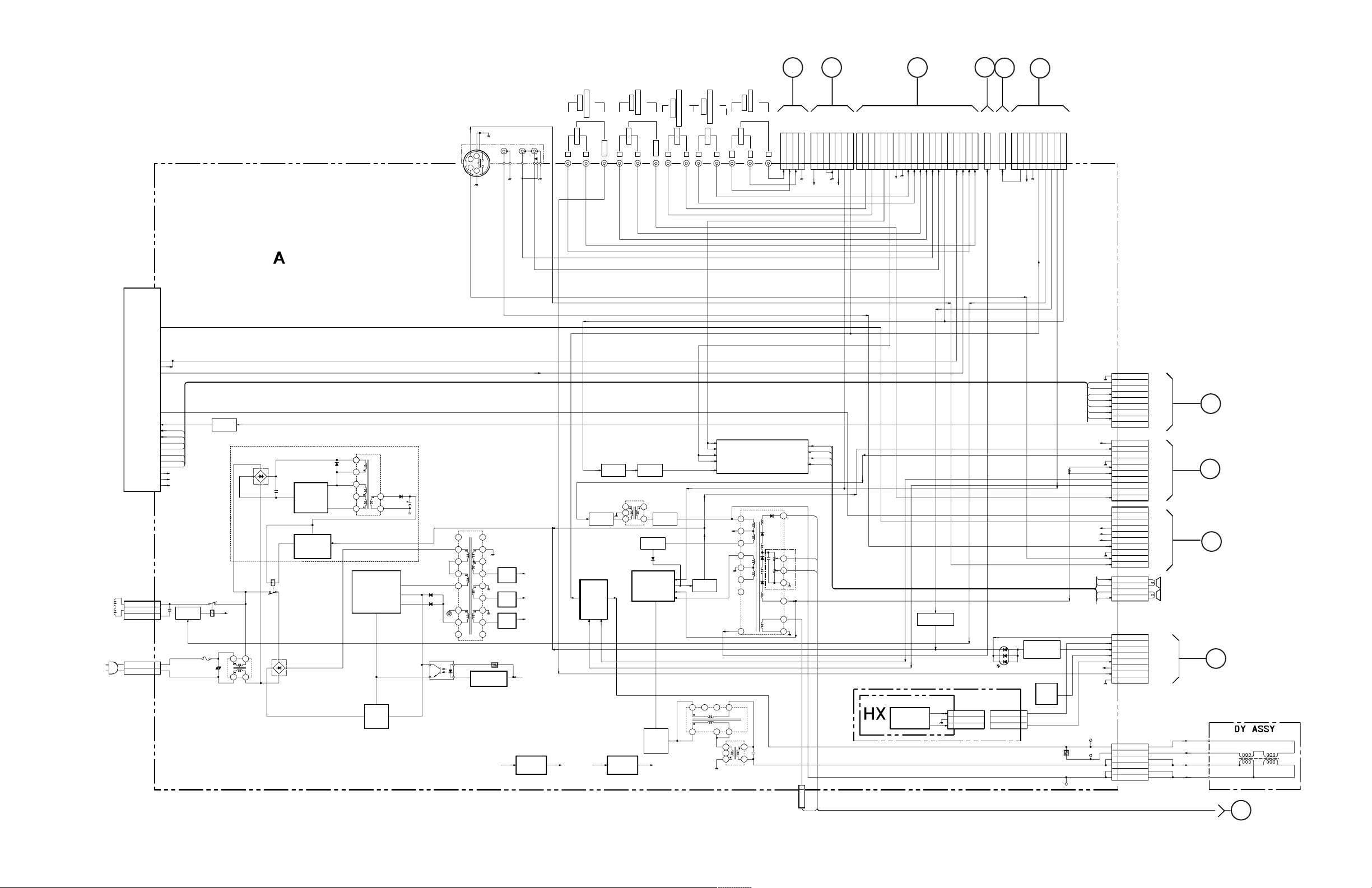
5-3. BLOCK DIAGRAM AND SCHEMATICS
KV-27FS13/ 27FS17/ 27FV17/ 29FV17/ 29FV17C/ 32FS13/ 32FS17/ 34FS13C/ 34FS17
BLOCK DIAGRAM (1 OF 6) (KV-27FS13/27FS17/32FS13/32FS17/34FS13C/34FS17 ONLY)
F
R
O
I
J
N
N
2
T
P
0
U
2
A
T
/
J201
S-VIDEO
Y
S
1
3
V
L
4
2
C
(POWER SUPPLY)
(DEFLECTION)
(TUNER/IF)
(AUDIO)
(MTS)
TU101
CLOCK
DE-EM OUT
L OUT
R OUT
DATA
RF AGC
F MONO
MODE
SAP LED
ST LED
DET-OUT
VIDEO
AFT OUT
CN603
DGC
DGC
NC
DGC
CN602
AC IN
AC IN
AC
AC
9V
9V
30V
30V
5V
5V
3
2
DGC DRIVER
1
Q609
2
1
VDR601
RY601
DGC RELAY
F601
AGC
Q101
D622
D4SB60L-F
AC RECT
LOW B
T602
1
2
3
4
D4SB60L-F
AC RECT
RY602
RELAY
AC POWER
STANDBY CIRCUIT
CONVERTER
Q605
PROTECT
Q606
SWITCH
Q608
STBY DRIVE
Q607
D623
1
3
4
5
6 8
CONVERTER
IC601
OCP/FB
T604
SRT
:STAND BY
D626
9
C636
1
T603
D
VIN
S
PH600
PHOTOCOUPLER
3
18
5
16
4
15
3
17
2
13
14
8
12
7
11
9
10
R645
ERROR AMP
10k
IC602
124
D605
SW
Q601,602
Q603
LOW B LOW B5V 9V
R
+B
+B
RECT
LOW B
LOW B
RECT
AUDIO
AUDIO
VCC
RECT
+B
5V REG
IC604
V
A
U
D
I
O
L
R
H DRIVE
Q501
V OUT
IC502
OUTREF
+
E
E
V
V
I
I
R
R
D
D
V
I
D
E
O
VOL-CTRL
R
L
L
R
C
-
-
-
-
N
V
V
2
2
T
T
V
V
9
7
8
6
0
1
1
1
1
2
CN4001 CN2003
1
POWER-SW
2
GND
3
KEY-SW
D
E
6
4
0
0
5
5
N
N
C
C
M
F
V
D
1
1
D2001
POWER-SW
GND
KEY-SW
STBY 7.5V
F
8
0
0
2
N
C
V
5
.
T
Y
7
W
M
S
Y
P
V
B
S
T
S
9
7
8
IR DETECT
1
2
3
D
N
G
6
IC2001
E
O
C
A
P
T
R
G
L
U
H
P
D
E
M
R
I
1
2
3
4
5
9
GND
8
O-MONO
7
O-SAP
6
I-SAP
5
I-STEREN
AGC MUTE
I-HLDWN
MONITOR
SPK R+
SPK R-
SPK L+
LED-TIMER
POWER-SW
IR(SENSOR)
MENU-SW
KEY-SW
STBY +5V
V2(VIDEO2)
CN501
MAIN1
MAIN2
PIP-L
SDAT
30V
SET9V
SPK L-
CN406
V DY+
V DY-
H DYH DY-
H DY+
H DY+
CN2007
AFT
HD
GND
CN2006
ABL
EW
VD+
VD-
V3
SCL
SET5V
CN2005
V1
GND
Y1
C1
+
SPR
+
SPL
4P
CN2001
GND
4
3
2
1
10
SET9V SET9V
9
8
7
6
5
4
3
2
1
10
9
8
7
SET5V
6
30V
5
SET9V
4
3
2
1
1
2
3
4
1
2
3
4
5
STBY
6
+5V
7
BA5-911-FS-BD
8
6
5
4
3
2
1
S2007
S2008
TP508
TP507
TP 506
G
H
I
J
V DY(+)
V DY(-)
H DY(-)
H DY(+)
A B C
R
E
A
I
J
R
N
2
VOL-CTRL
O
0
U
3
T
P
U
T
V
I
D
E
O
L
Q411
P
A
U
/
T
V
A
U
D
I
O
L
R
Q410
T501
4
1
9V REG
IC603
2
3
V HOLD
CNTRL
IC501
6
PIN DRIVE
H OUT
Q502
OCP
Q505
IN+1
OUT2
IN-1
1
T
U
IN+2
O
Q503
PIN OUT
Q504
Y
R
C
E
B
A
C
R
I
J
J
R
N
2
4
V
P
A
A
0
0
U
5
2
R
U
T
/
D
F
I
I
O
X
A
A
U
U
D
D
I
I
O
O
L
R
R
Y
,
P
I
J
R
N
2
,
P
0
P
U
6
B
T
1
0
3
N
A
U
D
I
O
PBP
R
C
V
U
Y
R
B
C
C
O
Y
T
-
Y
1
2
3
5
1
5
N
C
L
R
-
-
R
L
X
D
V
N
D
D
C
5
G
N
N
N
3
G
G
1
4
1
4
2
3
X
-
I
I
+
N
N
F
P
F
V
D
O
O
H
9
5
/
/
V
M
M
R
R
A
A
V
V
4
3
2
1
6
7
0
6
4
N
C
L
L
R
R
L
R
R
L
D
-
-
-
V
N
T
V
T
9
G
U
U
U
O
Y
O
7
5
6
8
9
9V
E
-
-
-
-
-
T
V
3
1
1
3
U
U
V
V
V
V
M
Y
5
4
3
2
1
0
1
1
1
1
1
1
+B 9V
Q506,507
0
1
1
IN1+
IN2+
IN3+
IN4+
MUTE
SW
8
9
3
T504
AUDIO AMP
1
4
200V
2
7
8
9
0
DF
0
7
T503
4
1
5
234
IC402
OUT1+
OUT3-
OUT4+
OUT2-
HV
T505
FBT
FV
G2
11
ABL
FUNCTION
SWITCHES
RELAY DRIVE
Q604
6
H
5
(KEY)
CN502
6
H
E
A
T
E
R
K
— 25 —
Page 26
KV-27FS13/ 27FS17/ 27FV17/ 29FV17/ 29FV17C/ 32FS13/ 32FS17/ 34FS13C/ 34FS17
BLOCK DIAGRAM (2 OF 6) (KV-27FS13/27FS17/32FS13/32FS17/34FS13C/34FS17 ONLY)
1
135V
NC
GND
CN800
CN802
GND
9V
HP
VD+
DF
B
D
+B
2
3
4
9V
5
6
7
BUFFER
Q801
1
Q803,804 Q802
SW BUFFER
(CONVERGENCE)
HP HP
Q812 IC803
SW BUFFER
Q810 Q809
V MOD
IC801
DF-COMP
Q805,806
QP DRIVE
Q811
IC802
V MOD
CN801
1
QP DRIVE
2
9V DRIVE
3
V MOD
4
V MOD
E
QP DRIVE
9V DRIVE
CN904
1
2
3
V MOD
4
V MOD
CN901
5
VM
VELOCITY
( )
MODULATION
AMP
Q903
Q904
DRIVE
VM OUT
DQP
Q905
Q906
QP
H OUT
Q807Q808
VM
DRIVE
Q901
Q902
(AUDIO PROCESSOR)
CN450
1
MON-L
2
MON-R
VAR/FIX-R
VAR/FIX-L
C
3
4
5
OUT-L
6
OUT-R
7
9V
GND
YUV-L
YUV-R
V3-L
V3-R
V1-L
V1-R
MUTE
NC
TV-L
TV-R
V2-R
V2-L
9V
8
9
10
11
12
13
14
15
16
17
18
19
20
IN5A
IN4A
IN2A
IN1A
IN3A
OUT-A
OUT-B
IN5
IN4
IN2
IN1
IN3
AUDIO
PROCESSOR
IC404
LINEA
LINEB
MUTE
Q430,431
SCL
SDA
IN6
IN6A
Q432,433
BUFFER
QP QP VM
CN902
1
QP-
2
QP-
3
QP+
4
QP+
5
E
6
E
7
VM
8
VM
1
SCL
2
GND
3
SDA
CN402
CN451
1
PIP-R
PIP-L
2
8
QP-
7
QP-
6
QP+
5
QP+
4
E
3
E
2
VM
1
VM
VM
M
L
— 26 —
BA5-911-FS-BD
Page 27
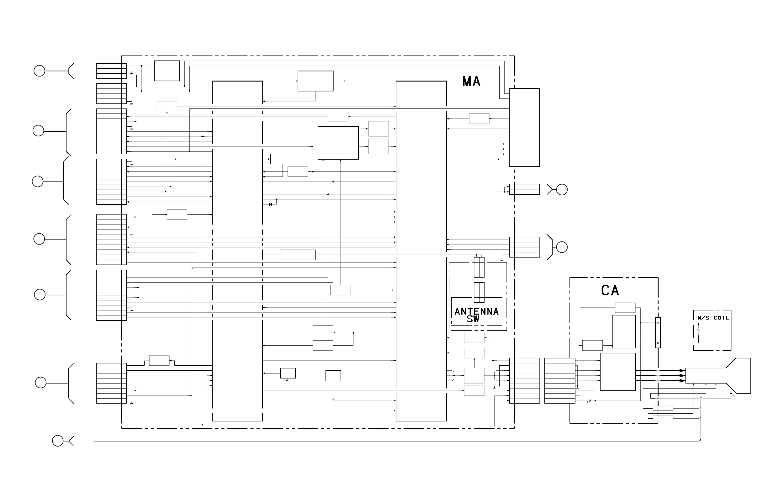
BLOCK DIAGRAM (3 OF 6) (KV-27FS13/27FS17/32FS13/32FS17/34FS13C/34FS17 ONLY)
3
M
CN309
CN002
FOR JIG
F
G
H
I
J
CN003
CN004
CN005
CN006
CN001
DAT
GND
B-CLK
RELAY
O-SAP
AFT
HD
GND
EW
VD-
PIP-L
SCL
30V
V1
GND
LED
GND
2
1
1
2
3
GND
4
9
8
VM
7
6
GND
5
4
DGC
3
HP
2
1
MUTE
9
GND
8
7
6
5
4
3
2
1
10
9
8
7
6
5
4
3
2
1
V3
10
9
8
7
6
5
4
3
Y1
2
C1
1
1
2
3
4
5
6
7
8
CLK
B-DAT
B-INT
SPSW
STBY 7.5V
I-PROT
O-MON0
I-SAP
I-STEREN
MAIN 1
MAIN 2
AGC MUTE
SET9V SET9V
I-HLDWN
ABL
VD+
MONITOR
SDAT
SET5V
SET9V
POWER-SW
IR(SENSOR)
MENU-SW
KEY-SW
STBY +5V
V2(VIDEO2)
STBY 7.5V
SET5V
SET9V
STBY +5V
BUFFER
Q004
MEMORY
IC003
BUFFER
Q001
BUFFER
Q003
BUFFER
Q002
IO-BCLKN
IO-BDAT
I-BINT
I-PROT
O-DGC
O-RELAY
O-MUTE
O-MONO
O-SAP
I-SAP
I-STEREN
I-AFT
O-AGCMUTE
I-HLDWN
CONTROL
TUNING SYSTEM
O-LED
I-POWER
I-RMCN
I-MENU
I-KEY
IC001
O-OSDBLCK
O-ANTSW
O-YUYSW
I-RESET
I-HSYNC
I-SDAT
O-SCLN
I-CVIN
I-BSC
O-OSC
O-N/S
O-YM
I-VPN
I-HP
STBY+7.5V STBY+5V
STBY+5V REG
IC002
RESET
VM OUT
Q375
DIG COMB
FILTER
IC302
N
A
L
I
D
C
A
S
BUFFER
Q349,358
Q359
BUFFER
Q305
S
BUFFER
Q310
X301
HSYNCH SEP
Q006
HP
Q365,082
O-R
O-G
O-B
SW
Q378,379,380
X1001
KV-27FS13/ 27FS17/ 27FV17/ 29FV17/ 29FV17C/ 32FS13/ 32FS17/ 34FS13C/ 34FS17
TU150
(TUNING CONTROL)
(Y/C/J)
CVBS4IN
VM
COUT
Q302,354
BUFFER
COMB C
VBSS-IN
I-AFT2
(2ND TUNER)
BUFFER
Q150,151
Q369,370
YOUT
N
I
K
C
BUFFER
Q350,351
Q352,355
COMB Y
Y/C JUNGLE
9V
30V
5V
IC301
HP PROTECT
SDA
SCL
YS2/YM
R2IN
G2IN
B2IN
HD
ABLIN
EW
VD+
CVBS3IN
CVBS2IN
FSC-OUT
CVBS1IN
VTIM
Y1
C1
MONOUT
YUYSW
XTAL
VD-
DVD-YIN
DVDCR-IN
DVDCB-IN
AFCFI
IKIN
ROUT
GOUT
BOUT
H-VD
IK BUFFER
BUFFER
R,G,B OUT
Q387,388
CONVERG
Q356
1
3
A
A
N
N
T
T
-
-
2
1
2
1
-
-
T
T
N
N
A
A
1
3
Q303
Q368
Q389
CLOCK
DATA
MUTE
DET-OUT
AFT OUT
9V
30V
5V
DE-EM OUT
1
2
1
2
3
4
1
2
3
4
5
6
7
8
9
CN401
PIP-R
PIP-L
CN302
Y-TO-YUV
CN303
NS MUTE
H TRAP
L
YCR
YCB
GND
IK
GND
R
B
G
GND
N/S
CN705
NS MUTE
IK
GND
GND
N/S
H TRAP
A
(RGB DRIVE)
(CRT DRIVE)
N/S MUTE
Q700
N/S
DRIVE
IC1701
N/S MUTE
Q701
1
2
R
3
B
4
G
5
6
7
8
9
NS IN
CRT
IK
DRIVE
IC702
R IN
B IN
R OUT
B OUT
G IN G OUT
CN706
BA5-911-BD
CN701
KR 12
KB 10
KG 11
CN704
FOCUS
1
3
1G2
HEATER6
N/S COIL -
N/S COIL +
PICTURE TUBE
H
G2FV
HV
K
— 27 —
Page 28

BLOCK DIAGRAM (4 OF 6) (KV-27FV17/29FV17/29FV17C ONLY)
BA5-911-FV-BD
1
2
3
4
5
6
7
8
9
1
0
1
1
1
2
1
3
1
4
1
5
1
6
1
7
1
8
1
9
2
0
1
2
3
4
1
3
2
4
6
1
2
1
2
3
1
2
3
4
5
6
7
8
9
10
1
2
3
4
5
6
7
8
9
10
1
2
3
4
5
6
7
8
9
1
2
3
4
5
6
7
8
9
1
3
4
7
8
9
1
0
1
2
3
4
1
2
3
4
5
6
7
8
9
1
2
3
4
5
1
2
3
4
V
L
R
S
1
2
3
4
1
2
3
4
5
7
8
9
10
11
12
14
15
16
17
13
18
124
3
1
2
3
4
5
6
1
234
5
1
2
3
1
2
3
1
2
3
4
5
6
7
1
2
3
4
5
6
7
8
9
10
11
C
N
4
6
0
T604
RY601
RY602
C636
D622
VDR601
D605
R645
T505
T501
CN602
CN603
CN2005
CN2006
CN2007
C
N
2
0
0
8
T503
C
N
3
0
1
J201
D626
F601
T602
T603
PH600
CN501
T504
CN4001 CN2003
C
N
5
1
5
CN2001
CN406
CN503
CN2004
SRT
:STAND BY
DGC RELAY
RELAY
AC POWER
D4SB60L-F
AC RECT
D4SB60L-F
AC RECT
10k
FBT
S-VIDEO
PHOTOCOUPLER
VIDEO
MAIN1
ST LED
I-STEREN
SAP LED
I-SAP
MODE
O-SAP
F MONO
O-MONO
GND
MAIN2
AFT OUT
AFT
RF AGC
AGC MUTE
AGC
Q101
9V
30V
5V
L OUT
DE-EM OUT
R OUT
M
U
T
E
VOL-CTRL
Q410
T
V
-
L
T
V
-
R
V
2
-
L
V
2
-
R
CLOCK
DATA
V
1
-
R
V
1
-
L
Y
U
V
-
R
Y
U
V
-
L
A
U
D
I
O
L
R
G
N
D
9
V
O
U
T
-
R
O
U
T
-
L
SPK R+
SPK R-
SPK L+
SPK L-
GND
GND
V1
V
M
1
3
4
5
6 8
9
STANDBY CIRCUIT
D623
Q606
PROTECT
Q605
CONVERTER
SWITCH
Q608
STBY DRIVE
Q607
R
E
L
A
Y
DGC
DGC
DGC
DGC DRIVER
Q609
D
G
C
D
VIN
S
OCP/FB
+B
FV
G2
5
6
9
8
7
2
4
1
0
0
11
DF
HV
H OUT
Q502
H DRIVE
Q501
HD
H
P
EW
PIN DRIVE
PIN OUT
Q504
Q503
I-HLDWN
VD+
G
N
D
I
-
P
R
O
T
S
T
B
Y
7
.
5
V
VD-
ABL
DET-OUT
CONVERTER
IC601
5V REG
IC604
9V REG
IC603
ERROR AMP
IC602
IC501
V HOLD
CNTRL
V OUT
IC502
SPR
SPL
+
+
AC IN
TU101
M
O
N
-
L
M
O
N
-
R
V
A
R
/
F
I
X
-
R
V
A
R
/
F
I
X
-
L
S
P
S
W
MONITOR
V3
9V
30V
5V
SET5V
SET9V
30V
9V
STBY 7.5V
CN502
V
3
-
L
V
3
-
R
PIP-L
IR(SENSOR)
POWER-SW
LED-TIMER
GND
V DY+
V DY-
H DY-
H DYH DY+
H DY+
Y
C
B
C
R
A
U
D
I
O
I
N
P
U
T
VOL-CTRL
Q411
AUDIO AMP
NC
V
I
D
E
O
A
U
D
I
O
L
R
J
2
0
3
R
E
A
R
A
/
V
SET9V SET9V
J
2
0
5
A
U
D
I
O
L
R
J
4
0
2
R
E
A
R
V
A
R
/
F
I
X
POWER-SW
GND
KEY-SW
SWITCHES
FUNCTION
POWER-SW
GND
KEY-SW
TP507
TP508
TP 506
200V
A
U
D
I
O
Y
-
T
O
-
Y
U
V
C
R
C
B
G
N
D
V DY(+)
V DY(-)
H DY(-)
H DY(+)
Y
PBP
R
J
2
0
6
Y
,
P
R
,
P
B
I
N
P
U
T
I
N
P
U
T
+B 9V
D
F
C
N
5
0
4
LOW B LOW B5V 9V
LOW B
AUDIO
LOW B
VCC
+B
RECT
+B
RECT
LOW B
RECT
AUDIO
O
U
T
P
U
T
(POWER SUPPLY)
(DEFLECTION)
(TUNER/IF)
(AUDIO)
(MTS)
(KEY)
IC402
MUTE
IN1+
IN2+
IN3+
IN4+
AC IN
AC
AC
M
U
T
E
N
C
9
V
1
3
5
V
N
C
G
N
D
G
N
D
H
P
V
D
+
V
M
RELAY DRIVE
Q604
SW
Q506,507
SW
Q603
Q601,602
D
R
I
V
E
+
OUTREF
D
R
I
V
E
-
IN+1
IN-1
O
U
T
1
OUT2
IN+2
OCP
Q505
OUT1+
OUT3-
OUT4+
OUT2-
1
ABL
H
1
C
N
5
0
6
J
2
0
4
M
O
N
I
T
O
R
O
U
T
P
U
T
V
I
D
E
O
A
U
D
I
O
L
R
BUFFER
Q201
BUFFER
Q402
BUFFER
Q401
MUTE
Q205,206
GND
Y2
C2
GND
GND
NC
FRONT V
FRONT Y
FRONT C
FRONT R
FRONT L
MENU SW
GND
IR SENSOR
STBY 5V
LED-TIMER
LED-MPWR
Y
C
H
E
A
T
E
R
6
Y1
C1
SDAT
SET9V
30V
SET5V
SCL
STBY
+5V
STBY
+5V
V2(VIDEO2)
STBY +5V
KEY-SW
MENU-SW
KV-27FS13/ 27FS17/ 27FV17/ 29FV17/ 29FV17C/ 32FS13/ 32FS17/ 34FS13C/ 34FS17
A
B
C
D
F
E
G
H
I
J
K
L
M
— 28 —
Page 29
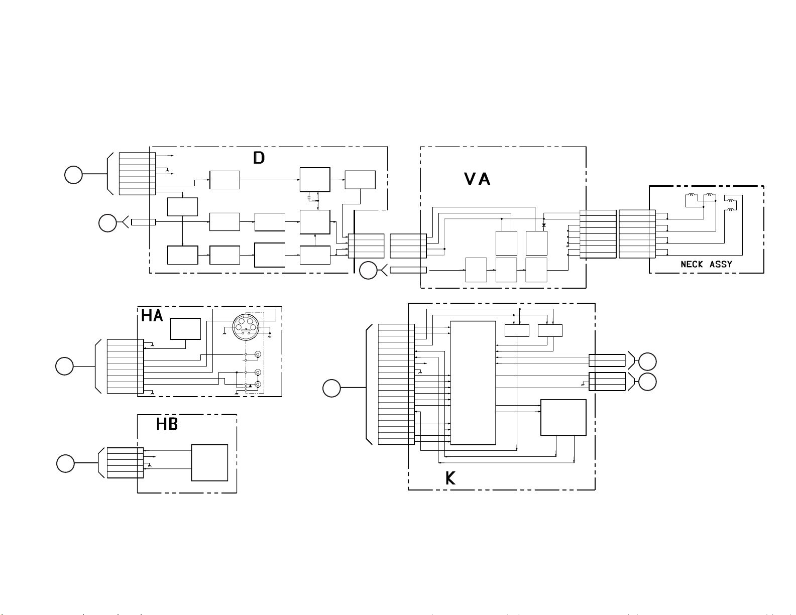
BLOCK DIAGRAM (5 OF 6) (KV-27FV17/29FV17/29FV17C ONLY)
1
135V
NC
GND
D
CN4200
MENU SW
FRONT V
FRONT Y
FRONT C
FRONT R
FRONT L
IR SENSOR
STBY 5V
LED-TIMER
LED-MPWR
GND
GND
GND
NC
CN4050
GND
9V
HP
VD+
CN800
CN802
DF
(FRONT A/V)
(MENU KEY)
1
2
3
4
5
6
7
8
9
1
2
3
4
5
B
K
G
2
3
4
5
6
7
1
Q803,804 Q802
(IR DETECTOR)
STBY
5V
+B
9V
BUFFER
Q801
SW BUFFER
FUNCTION
SWITCHES
IR DETECTOR
IC4050
(CONVERGENCE)
HP HP
Q812 IC803
SW BUFFER
Q810 Q809
S
Y
34
12
J4221
FRONT
VIDEO 2
V
L
R
V MOD
IC801
C
DF-COMP
IC802
V MOD
Q805,806
QP DRIVE
Q811
CN801
1
QP DRIVE
2
9V DRIVE
3
V MOD
4
V MOD
QP DRIVE
9V DRIVE
CN904
V MOD
V MOD
CN901
E
CN450
MON-L
MON-R
VAR/FIX-R
VAR/FIX-L
OUT-L
OUT-R
9V
GND
YUV-L
YUV-R
C
V3-L
V3-R
V1-L
V1-R
MUTE
NC
TV-L
TV-R
V2-R
V2-L
KV-27FS13/ 27FS17/ 27FV17/ 29FV17/ 29FV17C/ 32FS13/ 32FS17/ 34FS13C/ 34FS17
VELOCITY
( )
MODULATION
Q430,431
QP
H OUT
Q807Q808
VM
DRIVE
Q901
Q902
MUTE
BUFFER
Q432,433
L IN
R IN
L OUT R OUT
AUDIO
FILTER
IC403
BA5-911-FV-BD
1
2
3
4
MONB
MONA
IN5
IN5A
IN4
IN4A
IN2
IN2A
IN1
IN1A
IN3A
IN3
AMP
Q903
Q904
AUDIO
PROCESSOR
IC404
(AUDIO PROCESSOR)
5
VM
1
2
3
4
5
6
7
9V
8
9
10
11
12
13
14
15
16
17
18
19
20
DQP
DRIVE
VM OUT
Q905
Q906
LINEA
LINEB
IN6
IN6A
SCL
SDA
OUT-B
OUT-A
CN902
1
QP-
2
QP-
3
QP+
4
QP+
5
E
6
E
7
VM
8
VM
CN451
1
PIP-L
2
PIP-R
1
SCL
2
GND
3
SDA
CN402
8
QP-
7
QP-
6
QP+
5
QP+
4
E
3
E
2
VM
1
VM
N
0
QP QP VM
VM
— 29 —
Page 30
BLOCK DIAGRAM (6 OF 6) (KV-27FV17/29FV17/29FV17C ONLY)
KV-27FS13/ 27FS17/ 27FV17/ 29FV17/ 29FV17C/ 32FS13/ 32FS17/ 34FS13C/ 34FS17
3.3V REG
(Y/C SEP)
(AUTO WIDE)
COMB Y
COMB C
RESET
CN3500
GND
Y-IN
GND
CLK
GND
1
IN
2
3
4
GND
5
6
7
8
9
DAT
10
11
9V
12
13
5V
14
GND
15
C IN
BUFFER
Q3504,3505
BUFFER
Q3501,3502
Q3503
9V
5V
MEMORY
IC3500
CN306
1
IN
2
CN401
2
PIP-L
1
N
PIP-R
TU150
DE-EM OUT
AFT OUT
DET-OUT
9V
30V
5V
DATA
CLOCK
MEMORY
9V
30V
IC003
5V
(<TUNING CONTROL>)
(2ND TUNER)
(Y/C/J)
9V
5V
MUTE
GND
3
COMB Y
4
GND
5
COMB C
6
RESET
7
Y-IN
8
GND
9
DAT
10
CLK
11
9V
12
GND
13
5V
14
GND
15
C IN
IC3502
BUFFER
Q3501,3502
Q3503
BUFFER
Q3506
BUFFER
Q3510,3511
Q3512,3513
*RAS
*WE
*LCAS MCAS
*UCAS
(MA8)
(MA0-MA7)
(I01-I16)
5V3.3V
CSI
RSTB
AYI
AYO
ACO
SDA
SCL
MRAS
MWE
3D COMB FILTER
(MA8)
(MA0-MA7)
IC3501
BUFFER
X3500
20MHz
Q3500
I
O
C
S
F
O
I
X
X
C
S
F
(MI00-MI15)
3
DAT
CN309
GND
O
CN002
FOR JIG
F
H
I
J
L
CN003
CN004
CN005
CN006
CN001
2
CLK
1
B-CLK
1
B-DAT
2
B-INT
3
GND
4
9
SPSW
8
VM
7
STBY 7.5V
6
GND
5
I-PROT
4
DGC
3
RELAY
2
HP
1
MUTE
9
GND
8
O-MON0
7
O-SAP
6
I-SAP
5
I-STEREN
4
MAIN 1
3
MAIN 2
2
AFT
1
AGC MUTE
10
SET9V SET9V
9
I-HLDWN
8
HD
GND
7
ABL
6
EW
5
VD+
4
3
VD-
2
MONITOR
1
V3
PIP-L
10
SDAT
9
SCL
8
7
SET5V
6
30V
5
SET9V
V1
4
GND
3
Y1
2
C1
1
LED
1
2
POWER-SW
3
IR(SENSOR)
MENU-SW
4
KEY-SW
5
STBY +5V
6
V2(VIDEO2)
7
GND
8
9
Y2
10
GND
11
C2
STBY 7.5V
STBY +5V
BUFFER
Q001
BUFFER
Q003
BUFFER
Q301
SET5V
30V
SET9V
BUFFER
Q004
IO-BCLKN
IO-BDAT
I-BINT
I-AFT2
I-PROT
O-DGC
O-RELAY
O-MUTE
O-MONO
O-SAP
I-SAP
I-STEREN
I-AFT
O-AGCMUTE
CONTROL
TUNING SYSTEM
IC001
I-HLDWN
O-MONSW
O-LED
I-POWER
I-RMCN
I-MENU
I-KEY
I-HSYNC
I-BSC
O-OSC
I-RESET
I-SDAT
O-YM YS2/YM
O-OSDBLCK
I-VPN
O-YUYSW YUYSW
O-ANTSW
O-N/S
STBY+7.5V STBY+5V
X1001
O-R
O-G
O-B
STBY+5V REG
IC002
RESET
Q365,082
HSYNCH SEPBUFFER
HP
Q002 Q006
BUFFER
Q304,306
Q378,379
BUFFER
Q151,152
VM OUT
Q375
SW
Q380
BUFFER
Q305
X301
COMBC IN O-3DRESET
VBSSIN
CVBS4IN
VM
HP PROTECTI-HP
SDA
SCLO-SCLN
Y/C JUNGLE
R2IN
IC301
G2IN
B2IN
VTIM
HD
ABLIN
EW
VD+
C OUT
CVBS3IN
CVBS2IN
CVBS1IN
Y1
C1
MONOUTI-CVIN
COMB Y
XTAL
Y2 IN
C2 IN
VD-
PIP-CB-IN
PIP-CR-IN
DVD-YIN
DVDCB-IN
DVDCR-IN
PIP-OUT
PIPY-IN
IKIN
AFCFI
ROUT
GOUT
BOUT
H-VD
1
2
T
N
A
2
T
N
A
1
ANTENNA
IK BUFFER
Q303
BUFFER
Q368
R,G,B OUT
Q387,388
Q389
CONVERG
Q356
5V
9V
9V
3
2
4
1
CN304
D
-
V
N
T
9
G
N
A
1
D
-
V
N
T
9
G
N
A
3
2
4
9V
SW
CN305 CN3300
5V
1
2
DVD-Y
3
GND
4
DVD-B-Y
5
GDN
6
DVD-R-Y
7
9V
8
VIDEO
9
GND
10
MAIN VP
11
GND
12
P-B-Y
13
P-R-Y
14
P-Y
15
PYS
16
DAT
17
CLK
18
GND
19
MAIN SCP
20
MAIN HP
CN302
1
Y-TO-YUV
2
CR
3
CB
4
GND
CN303
1
IK
GND
2
3
R
B
4
G
5
GND
6
N/S
7
NS MUTE
8
H TRAP
9
DVD B-Y
DVD R-Y
MAIN VP
MAIN SCP
MAIN HP
DVD Y
VIDEO
CN705
GND
GND
GND
GND
P BY
P RY
P Y
P YS
DAT
CLK
GND
NS MUTE
H TRAP
5V
9V
5V
1
2
3
4
5
6
7
9V
8
9
10
11
12
13
14
15
16
17
18
19
20
A
3.3V REG
9V 3.3V
Q3304
(RGB DRIVE)
(CRT DRIVE)
N/S MUTE
Q700
N/S MUTE
Q701
1
IK
GND
2
3
R
B
4
G
5
GND
6
N/S
7
8
9
IK
CRT DRIVE
IC702
R IN
B IN
G IN
NS IN
N/S DRIVE
R OUT
B OUT
G OUT
Q3312,3310
IC1701
BUFFER
BUFFER
BUFFER
BUFFER
BUFFER
BUFFER
CBVSIN
YIN
UIN
VIN
VD
Y(R)OUT
SWM
SDATA
SCLK
HD
U(G)OUT
V(B)OUT
PROCESSOR
IC3301
PIP
Q3300
Q3301
Q3302
DRIVE
Q3305
Q3308
Q3307
Q3309
SW
(PIP)
CN701
N/S COIL -
2
4
1
N/S COIL +
3
KR 12
KB 10
KG 11
FOCUS
CN704
1G2
CN706
6
HEATER
PICTURE TUBE
H
G2
FV
HV
M
BA5-911-FV-BD
— 30 —
Page 31

A BOARD SCHEMATIC DIAGRAM (KV-27FS13/27FS17/32FS13/32FS17/34FS13C/34FS17 ONLY)
1 | 2 | 3 | 4 | 5 | 6 | 7 | 8 | 9 | 10 | 11 | 12 | 13 | 14 | 15 | 16 | 17 | 18 | 19 | 20 | 21 | 22 | 23 |
A
—
B
—
C
—
D
—
E
—
F
—
G
—
H
—
I
—
J
—
K
—
L
—
M
—
CN2005
TO MA BOARD
CN006
TO MA BOARD
CN602
TO MA BOARD
10P
SET 9V
SET 5V
CN2007
9P
CN004
AGC-MUTE
MAIN2
MAIN1
I-STEREN
I-SAP
O-SAP
O-MONO
2P
AC IN
AC IN
TO DGC 32
TO DGC
27/32
CN301
CN302
Y-TO-YUV
30V
SDAT
PIP-L
AFT
GND
CN603
DGC
DGC
DGC
DGC
CN604
CR
CB
GND
STEREO
TP100
RF-AGC
C219
10
C104
470
25V
1
C1
2
Y1
3
GND
4
V1
5
6
7
8
SCL
9
10
Q101
R105
2SD601A
4.7k
5.6V
AGC
V
V
0
9
3
C
C
C
C
V
V
L102
:CHIP
9V
E
V
L
K
5
B
A
C
A
T
O
C
N
A
L
C
E
D
V
C
R107
100
:CHIP
P
I
H
C
:
C102
100
1
0
1
L
R108
100
:CHIP
30V
0.0V
1
2
VIDEO
3
4
5
6
7
8
9
30V
D204
MTZJ-T-77-30D
30V REG
:40
S
C
R210
75
D206
RD9.1EW-T1
2
1
12
C
G
A
F
R
:CHIP
TP602
SET+5V
34
V
L
R
T
U
V
T
O
9
U
O
T
T
C
U
O
C
C
F
C
F
N
N
A
V
I
T
D
2
U
D
E
T
O
U
O
T
T
E
E
D
D
O
E
L
L
E
P
D
T
A
O
S
S
M
T
N
O
M
F
T
U
E
U
O
D
T
O
M
U
S
S
M
R
TP102
DET OUT
L103
C105
47
25V
VIDEO
TP101
SET 9V
R115
0
9V
RD9.1EW-T1
C204
0.0047
B:CHIP
R204
22k
:CHIP
MTZJ-T-77-10B
R205
33k
:CHIP
IC604
LM7805CT
5V REG
C657
47
25V
C205
4.7
:CI
Y
J201
4P
S-VIDEO
R214
470k
R208
15k
3W
D208
RD9.1EW-T1
C207
2.2
:CHIP
3
RD9.1EW-T1
R215
470k
UDZSTE-179.1B
12
+B
D205
D209
R648
33
3W
C208
2.2
D210
MTZJ-T-77-10B
JW664
15MM
9V
F601
3P
1
2
NC
3
1
2
NC
3
*
CB
Y
J206
3P
Y,CB,CR
CR
4P
RD9.1EW-T1
D215
RD9.1EW-T1
D214
1
2
3
4
RD9.1EW-T1
D211
9V
T
U
O
L
C100C101
00
D2003
MTZJ-T-77-10B
D213
STBY 7.5V
TU101
FSS BTF-WA412
TUNER
AUDIO L
PIN21
PIN22
PIN20
C216
4.7
D212
C210
4.7
LOW B
AUDIO R
STEREO
SAP MONO
4.9 0.3
0
0
0.3
4.9
STEREO MONO
0
5.0
R237
220
CHIP
R235
470k
R238
CHIP220
CHIP
R239
470k
CHIP
J202
FRONT A/V
V
L
R
3P
9V 9V 9V
STBY 7.5V
THP601
*
Q609
2SC3311A
DGC DRIVER
T602
*
VDR601
*
IC603
PQ09RD21
9V REG
JW613
5MM
JW614
5MM
1
4
IO
+B
C648
0.22
125V
C655
0.47
125V
R613
2.2M
+B
9V
D2001
LNK0120022G
R2005
0
STBY 5V
N
CN2003
3P
TO HX BOARD
—
O
—
P
CN4001
POWER-SW
KEY-SW
1
2
GND
3
0
9
8
7
6
5
1
CN2006 CN2008
10P 9P
CN005 CN003 CN001
N
V
W
9
D
D
-
L
H
T
H
E
-
S
I
4
+
D
L
W
D
N
B
E
V
G
A
D2002
MTZJ-T-77-10B
D2004 D2005
MTZJ-T-77-5.1C MTZJ-T-77-5.1C
8
7
6
5
4
3
3
2
1
R
O
T
3
D
V
I
V
N
O
M
9
V
W
5
D
M
S
.
N
V
P
7
G
S
Y
B
T
S
2
1
1
2
3
4
E
T
Y
O
C
A
P
R
G
L
H
P
D
E
R
I
R
W
T
U
M
R
E
W
S
O
M
S
-
S
I
-
R
N
T
U
E
E
-
N
W
S
D
E
O
R
E
M
P
I
L
8
5
6
7
V
W
5
2
S
V
-
Y
Y
B
E
T
K
S
CN2001
D
N
G
8P
TO MA BOARDTO MA BOARD TO MA BOARD
L605
13.9V
2
3
G
SBX3081-71
IR DETECT
C215
R421
1
4.7k
16V
C214
16V
1
F
D2SB60A-F04
AC RECT
R422
4.7
R603
470k
D623
BA159DGPPKG3
D624
1SS133T-77
FB608
:RN
D625
1SS133T-77
C637
0.001
*
D628
D1N20R-TA
C639
22
TH601
C641
10
D622
450V
V
8
.
0
Q605
4
2SK2663
CONVERTER
S
V
6
.
5
3
C
V
2
-
8
1
-
.
7
7
6
1
7
6
3
-
D
T
J
Z
T
M
C638
470p
-35.3V
R612
-36.1V
680
R616
6.8
1/2W
Q606
2SD601A
PROTECT
R602
4.7
:FPRD
C635
0.001
R617
22
7
7
-
8
T
1
3
6
3
D
1
S
S
1
C643
0.047
-36.3V
R608
22M
1/2W
R609
1k
R610
10k
CHIP
R611
47k
D627
MTZJ-T-77-7.5A
C604
0.0033
SET 9V
C634
0.01
250V
R614
470
STBY 7.5V
RY601
RELAY
D601
1SS133T-77
R635
2.2k
0.0V
CHIP
R634
10k
CHIP
R650 R658
0.68 0.68
L604
IC2001
123
R2003
4.7k
C2001
47
25V HDT
JW(5MM)
R636
R2002
LOW B
JW603
JW610
12.5MM
7.5MM
JW604
JW609
12.5MM
7.5MM
C607
*
125V
R601
*
1/2
Q507
R508
2SB709A
22k
0.0V
LOW B
R572
4.7k
:CHIP
0.0V
C628
100
25V
S2007 S2008
UP/DOWN
R2001
2.2k
CHIP1.5k
CHIP
R661
2.2k
R642
R663
22k
2SD601A
RELAY DRIVE
SW
47k
JW602
12.5MM
JW606
12.5MM
R615
0.0V
MENU/SEL
R2004
6.8k
CHIP
Q604
R607
22
Q607
2SD2144S-TP-UVW
C601
0.1
H.DRIVE
25V
CHIP
D612
C611
2200p
250V
TP500
R510 C535
330 0.47
STBY DRIVER
0.1V
0.7V
C602
47
C610
-33.3V
-33.3V
D603 R651
MTZJ-T-77-33B 10k
C609
100
R618
82k
C502
0.047
200V
93.3V
1
C501
470p
0.0V
R501
4.7k
2SC3209LK-TP
C506
0.001
D602
1SS133T-77
RY602
RELAY
AC POWER
MTZJ-T-77-10B
C606
2200p
250V
*
1W
R571
4.7k
:CHIP
Q506
2SD601A
SW
V
1
.
4
0.1V
:STAND BY
1
3
4
5
6 8
R653
1k
CHIP
R621
6.8
10W
10
-33.3V
R619
47k
RGP02-17PKG23
R547
560
2W
R502
560
2W
680
2W
2
C503
470p
500V
R503
4.7k
Q501
H DRIVE
T604
SRT
9
R630
2.2k
D605
D4SB60L-F
AC RECT
D606 R623
TF541M 470
D608
MTZJ-T-77-20B
R622
100k
Q601
2SD2144S-TP-UVW
D607
D604
+B
1
2
3
C504
470p
500V
R522
1k
0.2V
R523
10k
Q503
2SD601A
PIN DRIVE
10ELS2N-TA1B2
STBY RECT
C647
0.0047
250V
SW
R620 C613
T501
TP601
SET+9V
3.8V
KV-27FS13/ 27FS17/ 27FV17/ 29FV17/ 29FV17C/ 32FS13/ 32FS17/ 34FS13C/ 34FS17
CN460
L
T
I
N
O
M
1
R436
*
R438
*
+B
L601
JW(5mm)
C513
0.001
100V
B
C512
0.068
200V
L503
10mH
1SS133T-77
C534
10
1.8V
2SA1091O-TPE2
R546
0.47
TO K BOARD
CN450
C510
2.2
200V
200V
C553
22
250V
D516
:4A
R554
R555
470k
134.9V
Q505
OCP
20P
TDA8580Q/N1
AUDIO AMP
R437
*
CHIP
AUDIO VCC
L505
R513
10k
C531
0.068
200V
:PT
IC402
C403
0.22
JW(5mm)
L502
2.2mH
*
*
3W
RGP10GPKG23
RGP15GPKG23
C533
470
25V
15000
D511
L602
C659
25V
C550
250V
L510
0.0047
13V REG
1
D
+
1
N
1
P
G
T
P
V
U
O
1 2 3 4 5 6 7 8 9
AUDIO
L+OUT
C420
0.22
25V
F
C496C421
00
R490
*
:CHIP
PS401
LINK
C402
2200
25V
R441
R440
22k
100k
0.0V
C441
1
16V
R506
33 2W
*
C511
*
250V
R512
68 3W
JW542
SW502
R544
0.47
R568
C551
22
2W
200V
:RS
15MM
1
4
200V
2
7
8
D514
9
R550
0
0.47
1/2W
:FPRD
DF
0
13V
Y
-
B
2
D
G
T
N
A
U
A
I
O
T
D
S
R
E
F
+
+
F
2
1
U
N
N
B
I
I
AUDIO L AUDIO R
5.2V
2SD601A
VOL CTRL
AUDIO
L-OUT
Q410
MTZJ-T-77-10B
R446
33k
R426
22
:CHIP
C435
0.22
25V
GND04
:CHIP
-2
R401 R402
20k
:CHIP
R442
100
R447
4.7k
D401
R445
10k
+B
TP 508
V OUT
TP506
R551SW501
H OUT
22
3W
D502
GP08DPKG23
D503
GP08DPKG23
HV
TP504
200V
+B
T505
*
FV
13V
G2
JR522
ABL
R545
4.7k
1W 2.2mH
11
R535
100k
6
TP510
HEATER
H
5
L507
JR523
JR526
JR527
(POWER SUPPLY)
(DEFLECTION)
(TUNER/IF)
(AUDIO)
(MTS)
BA5-911-FS-A
+
4
3
N
N
I
I
10 11 12 13 14 15 16 17
C401
100
AUDIO
L-OUT
JW414
10MM
10k
:CHIP
5.2V
T
N
P
T
5
U
U
N
M
I
G
O
P
V
AUDIO
R-OUT
AUDIO
L+OUT
C442
4.7
R454
100
5.2V
Q411
2SB709A
VOL CTRL
1
VM
2
9V
3
E
4
NC
5
+B
-
2
3
D
2
E
-
+
9V
CN501
6P
WHT
8
:DY
6
V DY +
5
V DY -
4
H DY -
3
H DY -
2
H DY +
1
H DY +
9
HV
TO CRT
FOCUS
TO CA BOARD
G2
TO CA BOARD CN704
6
200V
5
NC
4
E
3
HEATER
2
-13V
+13V
1
1
135V
2
NC
GND
3
4
GND
5
9V
6
HP
7
12.5MM
V PULSE
JW599
CN504
TO D BOARD
CN802
DF
1
0
0
0
0
+
4
T
U
O
AUDIO
R+OUT
JW252
5MM
CN506
TO VA BOARD
CN901
H.DY H.DY V.DY V.DY
CN502
6P
:S-MICRO
TO CA BOARD
CN706
CN515
TO D BOARD
CN800
CN406
4P
+
1
SPK R+
2
SPK R-
3
SPK L-
4
SPK L+
SPR
+
SPL
5P
7P
L
R
R
L
L
R
R
-
-
2
2
V
V
9
0
1
J205
2P
L
R429
470k
RD9.1EW-T1
D230
YCBCR AUDIO
R
INPUT
R430
1k
R431
1k
R433
470k
RD9.1EW-T1
D231
2
E
R
-
-
T
C
V
1
U
V
N
T
V
M
T
8
7
6
5
1
4
1
1
1
1
R
L
1
V
3
1
L
R
L
D
-
-
-
-
N
V
V
3
3
G
U
U
V
V
Y
Y
2
1
0
9
1
8
1
1
AUDIO R
-
-
-
L
X
R
V
9
7
X
T
-
I
-
I
I
T
F
T
F
N
U
/
U
/
O
O
R
O
R
M
A
A
V
V
6
5
4
3
2
A
U
D
I
O
L
A
U
D
I
O
R
AUDIO L
J402
2P
L
R413
R414
470k
1k
D626
C636
330
STBY 7.5V
FB607
*
JR505
0
D203
RD9.1EW-T1
RD9.1EW-T1
D233
R203
75
D232
RD9.1EW-T1
V
L
R202
470k
R201
470k
REAR-VAR/FIX
R
R
RD9.1EW-T1
J203
REAR A/V
D201
R411
1k
R412
470k
3P
JR472
JW(5.0MM)
LOW B LOW BLOW B
AUDIO VCC
TP600
1
R638
*
PC123FY2
4
3
D509
8
7
6
5
C530
PH601
*
5
4
3
2
8
7
9
1
2
R564
CHIP
NJM2903M-TE2
V HOLD CONTROL
D619
MTZJ-T-77-10B
Q608
0.7V
2SD601A
SW
R655
1k
0.0V
CHIP
R637
R662
*
*
3W
3W
C612
*
250V
1/2W
R624
10k
Q602
2SC3311A
SW
R625
47k1SS133T-77
10
C509
C507
680p
2kV
1.2kV
C515
680p
2kV
9V
C505
C508
680p
0.01
100V
R627
R628
-32.8V
*
2kV
R631
*
3W
R629
R656
*
10k
R626
R660
*
*
1/2W
3W
C618
470p
*
C660
*
C661
*
*
-23.6V-32.9V
C555
*
1.2kV
ERC06-15S
C520
400V
D505
RU4AM-T3
133.0V
V
4
0
R504
.
JW(7.5MM)
1
R521
470
3
R520
47
2W
C521
2200p
500V
100p 500V
0.1V
Q504
KTC4370A
PIN OUT
0
R505
47
FB501
1.1UH
C525
4
6
C526
L501
8mH
RGP10GPKG3
V
5
.
6
-
FB502
1.1UH
Q502
*
H-OUT
2W
FB503
1.1UH
D506
C524
C540
220p
22
500V
250V
B
C539
22
250V
C527
22
13V
B
ERC06-15S
D501
*
C615
*
400V
D609
*
C616
*
1kV
FB600
0UH
FB609
0UH
C617
680p
1.5kV
:PP
FB601
0UH
R649
1k
IC601
CONVERTER
D
N
N
I
G
V
B
1
A
T
0
N
1
-
6
4
D
0
S
Q
E
1
1
*
D
R632 R641
S
12345
FB602
0UH
*2W*
B
F
/
P
C
O
R633
680
2W
R644
3.3k
D611
10ELS2N-TA1B2
R643
C619 C652
1.5k
470p
:PT
D613
10ELS2N-TA1B2
FB603
R646
*
0.001
0UH
D614
C620
10ELS2N-TA1B2
100
25V
PHOTOCOUPLER
-26.3V
-23.6V
Q603
-31.2V
2SA1309A
SW
R570
22k
C554
C614
0.1
220p
+B
D504
T503
C514
*
250V
C517
*
+B
R569
1.8
1/2W
R541
10k
13V
1SS133T-77
E
V
+
I
C
R
C
D
V
1 2 3 4 5 6 7
R540R548
10k4.7
R519
*
R536
1.8
1/2W
TH501
D507
:4A
C541
220
R538
330
2W
C542
47
R537
*
R514
*
CHIP
R525
R524 R526
8.2k
10k 22k
1SS133T-77
PMT
0
1
1
F
E
R
MA111-TX
8
9
3
T504
*
1
IC502
*
V OUT
C
C
V
OUT
R539
2.2
:FPRD
D512
D515
MA111-TX
D508
:4A
C528
0.0022
B:CHIP
R528
2.2k
D521
1SS133T-77
C536
470p
500V1k
R516
4.7k
7
4
345
D518
MTZJ-T-77-7.5X
TEMP CORR
1SS133T-77
HOLD DOWN REF
MTZJ-T-77-5.6C
9V
D517
:4A
R560
47k
1W
:RS
R561
120
TP501
2
-13V
765
+
T
E
S
V
O
I
O
R
B
D
-13V
R518
*
R517
0.0022
B:CHIP
C529
D510
GP08DPKG23
*
10k
TP502
+13V
OUT1
+VCC
1
IN-1
OUT2
2
IN+1
IN-2
3
-VCC
IN+2
4
R530
*
CHIP
C543
0.22
R529
T603
*
C630 C631
**
9V
-13V
C523
470
25V
GND01
D522
MA111-TX
*
TP503
H.PROT
R567
10k
:CHIP
R565
10k
IC501
:HC
18
C621
1500p
FB610
2kV
C622
680p 500V
D620
D5LC20U
AUDIO RECT
IC602
EA135-F12
ERROR AMP
0UH
R645
10k
FB604
0UH
C624
C623
100
680p
160V
500V
FB606
0UH
FB605
*
C625
*
25V
R659
10
1W
12
3
+B
L504
16
15
17
D615
RU4AM-T3
+B RECT
13
14
D616
D5LC20U
LOW B RECT
12
JW615
5MM
11
JW616
5MM
10
R639
2.2k
C627
0.1
R640
250V
1k
C548
*
+B
D513
RGP15GPKG23
-13V REG
R563
C537
22k
MA111-TX
C549
220
16V
22
D520
R511
R562
0.47
12k
D519
EGP20DPKG23
PROTECT
:4G
C546
22
R566
10k
C547
CHIP
0.01
F
B+
L603
R652
JW(5MM)
C654
10
160V
LOW B
C626
15000
25V
AUDIO VCC
C658
*
25V
R507
D
1k
I
1/2W
M
V
7
0
5
P
L506
T
10mH
R543
220k
:CHIP
R553R509
0.33
2W
R549
0.47
R557
R556
470k
1k
135.5V
13V
R559
R558
10k 100k
R533
*
R534
*
R532
4.7k
-13V
WHEN REPLACING T505 BE SURE TO CHECK THE VOLTAGE VALUE
AT (TP503). REFER TO THE SAFETY ADJUSTMENT SECTION
R564 SEE PAGES 14 AND 15.
NOTE: *= VARIANT, SEE PARTS LIST
— 31 —
Page 32

A BOARD SCHEMATIC DIAGRAM (KV-27FV17/29FV17/29FV17C ONLY)
1 | 2 | 3 | 4 | 5 | 6 | 7 | 8 | 9 | 10 | 11 | 12 | 13 | 14 | 15 | 16 | 17 | 18 | 19 | 20 | 21 | 22 | 23 |
KV-27FS13/ 27FS17/ 27FV17/ 29FV17/ 29FV17C/ 32FS13/ 32FS17/ 34FS13C/ 34FS17
A
—
B
—
C
—
D
—
E
—
F
—
G
—
H
—
I
—
J
—
K
—
L
—
M
—
N
—
O
—
P
TO MA BOARD
CN006
CN2007
TO MA BOARD
CN004
AGC-MUTE
I-STEREN
TO HA BOARD
CN4200
TO HX BOARD
POWER-SW
TO MA BOARD
CN302
Y-TO-YUV
IRSENSOR
LED-TIMER
LED-MPWR
TO HB BOARD
CN2005
SET 9V
SET 5V
10P
SDAT
PIP-L
STEREO
TP100
RF-AGC
C219
10
C104
470
25V
1
C1
Y1
2
3
GND
4
V1
5
6
30V
7
8
SCL
9
10
V
V
0
V
9
3
K
5
C
C
C
C
O
C
C
C
L
V
V
V
C
P
I
H
C
:
L102
:CHIP
1
0
9V 9V
1
L
9V
9P
1
AFT
MAIN2
MAIN1
I-SAP
O-SAP
O-MONO
MENU-SW
CN2003
GND
CN503
GND
GND
3P
2
3
4
5
6
7
8
9
9P
9
8
L2
7
R2
6
C2
Y2
5
V2
4
NC
3
2
1
VIDEO
D206
RD9.1EW-T1
CN4001
1
GND
2
DGC
GND
CN602
CN603
NC
DGC
4P
3
2P
2
1
3P
1
2
3
1
2
3
4
1
2
GND
3
4
5
KEY-SW
AC IN
AC IN
CN301
CR
CB
STBY-5V
CN4050
CN2004
5P
TO MA BOARD TO MA BOARD
9V
0
9
8
7
6
5
4
3
1
N
V
W
9
T
E
CN005 CN003
S
L
D
D
D
B
N
L
H
A
G
H
I
2
R
O
-
+
W
T
D
D
E
I
V
V
N
O
M
R221
AUDIO R
C214
16V
PIN21
PIN22
1
F
220
R403
4.7k
STEREO
0
0.3
STEREO MONO
0
R422
4.7
SAP MONO
4.9
0
5.0PIN20
R421
4.7k
A
T
C
A
T
U
F
C
F
N
A
O
R
V
I
E
D
TU101
T
C
C
F
N
N
A
T
C
U
V
T
E
G
O
9
U
L
A
O
B
T
D
2
U
D
E
T
U
O
O
T
T
E
E
D
D
O
E
L
L
E
P
D
T
A
O
S
S
M
T
N
O
M
F
T
T
U
E
U
U
O
D
T
O
O
M
U
S
S
M
R
L
9V
C105
R107
47
100
25V
:CHIP
C102
100
R108
100
:CHIP
TP101
SET 9V
TP102
DET OUT
L103
:CHIP
VIDEO
R115
0
AUDIO L
Q101
2SD601A
R105
4.7k
AGC
C215
1
16V
5.6V
0.0V
C204
0.0047
30V
30V
D204
MTZJ-T-77-30D
30V REG
:40
S
34
12
V
L
R
D211 C610
RD9.1EW-T1
JW621 JW622
7.5MM 7.5MM
B:CHIP
R204
22k
:CHIP
S
E
T
5
R205
V
33k
:CHIP
VIDEO
TP602
SET+5V
D205
RD9.1EW-T1
3
JW664
15MM
R208
15k
3W
D208
D209
C208
2.2
D210
Y,CB,CR
CR
CB
C657
47
25V
C205
4.7
:CI
R210
75
RD9.1EW-T1
CY
J201
S-VIDEO
UDZSTE-179.1B
R214
470k
R215
470k
:CHIP
MTZJ-T-77-10B
Y
D214 D215
RD9.1EW-T1 RD9.1EW-T1
12
C207
2.2
J206
IC604
LM7805CT
5V REG
R648
5.6
3W
R664
5.6
3W
+B
C100C101
00
9V 9V 9V
LOW B
8.6V
C648
0.22
125V
+B
R218
*
4.5V
R404
4.7k
0.3
4.9
R407
100
STBY 7.5V
Q609
2SC3311A
DGC DRIVER
C655
0.47
125V
R613
2.2M
F601
*
THP601
AUDIO L
T602
9.0V
AUDIO L
*
+B
9V
V
5
.
4
AUDIO R
D236
UDZSTE-179.1B
V
Q201 J204
2
.
2SB709A
0
BUFFER
V
Q402
1
.
2SB709A
0
BUFFER
Q401
2SB709A
BUFFER
R408
100
C211
470
UDZSTE-179.1B
R224
4.7k
R225
4.7k
UDZSTE-179.1B
D2SB60A-F04
AC RECT
C212
D234
4.7
C213
4.7
D235
D622
0.0V
Q205
2SD601A
MUTE
TH601
C641
10
450V
V
8
.
0
4
S
V
8
.
6
3
C638
470p
R612
680
2SD601A PROTECT
V
R226
75
R227
470k
R231
6.8k
-0.4V -0.4V
Q605
2SK2663
CONVERTER
V
6
.
5
R617
3
C
22
-
2
1
-
7
7
1
7
6
-
D
T
J
Z
T
M
-35.3V
-36.1V
R616
6.8
1/2W
Q606
L
R
R228
470k
0.0V
R232
6.8k
R602
4.7
R608
:FPRD
22M
1/2W
R609
C635
1k
0.001
R610
10k
CHIP
7
7
R611
-
8
T
1
47k
3
6
3
D
1
D627
S
S
MTZJ-T-77-7.5A
1
C643
0.047
C604
0.0033
SET 9V
LOW B
L605
JW613
5MM
JW614
5MM
13.9V
1
4
VDR601
*
RY601
RELAY
D601
1SS133T-77
R635
2.2k
0.0V
CHIP
R634
10k
CHIP
2
3
JW(5MM)
LOW B
R636
JW603
JW610
12.5MM
7.5MM
JW604
JW609
12.5MM
7.5MM
C607
*
JW607
7.5MM
R601
*
JW608
7.5MM
R508
LOW B
Q507
2SB709A
22k
0.0V
SW
R572
4.7k
:CHIP
0.0V
R2003
4.7k
C2001
47
25V HDT
12.5MM
JW602
12.5MM
0.0V
R607
22
D602
1SS133T-77
RY602
RELAY
AC POWER
R571
4.7k
:CHIP
Q506
2SD601A
MTZJ-T-77-10B
C606
0.0022
250V
SW
JW606
R615
*
R229
470k
Q206
2SD601A
MUTE
C634
0.01
250V
D623
BA159DGPPKG3
D624
1SS133T-77
C637
0.001
FB608
0UH
R614
470
2SD2144S-TP-UVW
C601
0.1
25V
CHIP
D612
C611
0.0022
250V
9V 9V
STBY 7.5V
V
0.1V
1
.
TP500
4
H.DRIVE
R510 C535
330 0.47
L604
IO
R650
0.68
R658
0.68
IC603
PQ09RD21
9V REG
G
C628
100
25V
R661
STBY 5V
D2002
MTZJ-T-77-10B
D2004 D2005
MTZJ-T-77-5.1C MTZJ-T-77-5.1C
8
7
6
5
4
3
2
1
3
V
9
T
V
O
5
W
D
R
.
S
M
N
P
7
P
V
G
-
-
S
I
Y
B
T
S
1
123456789
R
E
Y
T
C
A
P
U
G
L
H
M
D
E
R
W
E
S
M
-
I
R
T
E
-
W
D
O
E
P
L
V
R
W
W
5
O
S
S
-
S
-
-
Y
N
U
Y
B
E
N
E
T
S
E
K
S
R
M
I
10
11
CN2001CN2006 CN2008
11P10P 9P
D
2
V
2
D
2
N
C
N
Y
G
G
TO MA BOARD
CN001
2.2k
R663
22k
R642
47k
Q604
2SD601A
RELAY DRIVE
J203
MONITOR
C639
22
3P
R603
470k
1SS133T-77
D1N20R-TA
D203
RD9.1EW-T1
RD9.1EW-T1
:RN
1
3
4
D625
5
6 8
D628
D201
:STAND BY
V
L
R201
470k
R203
75
T604
SRT
D626
10ELS2N-TA1B2
STBY RECT
9
STBY 7.5V
Q607
STBY DRIVER
0.1V
0.7V
C602
47
-33.3V
-33.3V
MTZJ-T-77-33B 10k
C609
100
R618
82k
R630
2.2k
R653
D605
1k
CHIP
D4SB60L-F
AC RECT
C647
0.0047
250V
R621 R641
6.8
10W
D606 R623
TF541M 470
10
-33.3V
MTZJ-T-77-20B
R622
100k
2SD2144S-TP-UVW
D603 R651
R619
47k
D604
RGP02-17PKG23
1/2W
D608
R624
10k
Q601
SW
D607
R620
C613
R
C636
330
STBY 7.5V
MTZJ-T-77-10B
0.7V
Q608
2SD601A
SW
R637
R202
470k
RD9.1EW-T1
FB607
0UH
0.0V
*
C612
R625
47k1SS133T-77
D202
RD9.1EW-T1
D619
R655
CHIP
*
2SC3311A
REAR A/V
D233
1k
R662
*
Q602
SW
R414
R656
10k
R627
R628
+B
C507
R547
560
2W
R502
560
2W
680
2W
2
C502
0.047
200V
93.3V
C503
470p
500V
1
C501
470p
0.0V
R501
4.7k
2SC3209LK-TP
Q501
H DRIVE
R503
4.7k
T501
1
2
3
C504
470p
500V
LOW B
R522
3.8V
1k
0.2V
R523
10k
C506
0.001
Q503
2SD601A
PIN DRIVE
C509
17000p
680p
1.2kV
2kV
C515
680p
2kV
C505
C508
680p
0.01
2kV
100V
133.0V
V
0
R504
.
JW(7.5MM)
1
R521
470
TP601
SET+9V
R520
47
2W
C521
2200p
500V
100p 500V
0.1V
Q504
KTC4370A
PIN OUT
0
3
R505
47
FB501
1.1UH
L501
8mH
RGP10GPKG3
V
C525
5
.
6
-
4
6
C526
13V
1k
*
*
C660
-23.6V-32.9V
-32.8V
D506
C524
220p
500V
FB502
1.1UH
R660
*
*
C555
2700p
250V
D505
RU4AM-T3
4
2SD2578-YB
2W
FB503
1.1UH
B
Q502
H-OUT
C540
250V
R413
470k
R626
1/2W
C661
ERC06-15S
22
C539
250V
C527
R629
0.1
22
22
L
R631
C618
470p
*
0.047
*
*
B
ERC06-15S
D501
C520
630V
L
R
R
-
-
2
V
V
T
9
8
1
1
18
16
15
17
13
14
D5LC20U
LOW B RECT
12
11
10
R639
2.2k
R640
1k
C548
160V
RGP15GPKG23
R563
22k
MA111-TX
K
R
L
T
L
-
-
A
C
1
V
D
V
T
-
B
B
7
6
5
4
1
1
1
1
AUDIO L
AUDIO L
C621
1500p
2kV
D615
RU4AM-T3
+B RECT
D616
C622
680p 500V
JW617
5MM
JW618 C625
D620
5MM 1000
D5LC20U
AUDIO RECT
IC602
EA135-F12
ERROR AMP
C627
0.1
250V
22
+B
D513
-13V REG
C537
22
R562
12k
C546
22
D520
C549
220
C547
16V
0.01
L
2
V
0
J402
REAR-VAR/FIX
R
D232
RD9.1EW-T1
C615
0.022
400V
D609
RU-1P
C616
220p
1kV
FB600
0UH
FB601
0UH
FB609
0UH
C617
680p
1.5kV
:PP
R649
1k
-23.6V
C614
0.1
D504
C514
0.68
250V
+B
R569
1.8
1/2W
R541
10k
13V
TH501
D507
1SS133T-77
:4A
IC601
CONVERTER
D
N
G
B
1
A
T
0
N
1
-
6
4
D
0
S
Q
E
1
1
Q603
2SA1309A
R411
1k
R412
470k
R429
470k
RD9.1EW-T1
JR505
*
B
F
/
N
P
I
C
V
O
S
D
12345
FB602
0UH
R633
R632
0.1
1
2W
2W
L
R430
10ELS2N-TA1B2
:PT
1k
R644
3.3k
D611
R643
1.5k
C652
0.001
D230
0
680
C619
470p
-26.3V
-31.2V
SW
R570
22k
C554
220p
R516
4.7k
J205
YCBCR AUDIO
R
INPUT
R431
1k
1SS133T-77
D231
RD9.1EW-T1
D613
10ELS2N-TA1B2
FB603
C620
10ELS2N-TA1B2
100
25V
D521
R638
0UH
*
D614
4
3
PH601
PC123FY2
PHOTOCOUPLER
D509
MTZJ-T-77-5.6C
9V
R433
470k
R646
*
C536
470p
500V1k 10
+B
MTZJ-T-77-7.5X
R517
10k
OUT1
1
IN-1
2
IN+1
3
-VCC
4
HOLD DOWN REF
TP501
-13V
R560
47k
1W
:RS
D518
TEMP CORR
D517
1SS133T-77
:4A
R561
120
-13V
TP502
+13V
+VCC
OUT2
IN-2
IN+2
15k 0.0022
8
7
6
5
NJM2903M-TE2
V HOLD CONTROL
T503
PMT
0
9
1
1
T504
5
E
V
+
I
C
R
C
D
V
1 2 3 4 5 6 7
R540R548
10k4.7
R519 R533
6.8k 33k
R536
1.8
1/2W
C541
220
R538
330
2W
R537
JW(5MM)
R514
22k
R525
R524 R526
8.2k
10k 22k
1SS133T-77
IC502
TDA8172
V OUT
F
-
E
C
R
C
V
C542
47
R539
2.2
:FPRD
D512
MA111-TX
D508
:4A
R528
2.2k
7
8
3
4
345
1
2
76
+
T
E
S
V
O
I
O
R
B
OUT
D
R518
6.8k
C543
0.22
D510
GP08DPKG23
D515
MA111-TX
C529
C528
0.0022
0.0022
B:CHIP
B:CHIP
330k
R529 R530 C530
2
AUDIO R
AUDIO R
1
5
4
3
2
8
7
9
T603
*
C630 C631
**
1
2
9V
-13V
C523
470
25V
D522
MA111-TX
R564
180k
TP503
H.PROT
R567
10k
:CHIP
R565
10k
IC501
:HC
A
L
1
V
3
1
FB610
0UH
FB604
0UH
C623
680p
500V
3
EGP20DPKG23
PROTECT
F
R
L
R
L
-
D
-
-
-
V
N
V
3
3
U
G
U
V
V
Y
Y
0
2
1
9
8
1
1
1
LOW B
TP600
L603
R645
10k
C624
100
160V
FB606
0UH
FB605
0UH
R659
10
1W
12
+B
L504
R549
0.47
R511
0.47
D519
:4G
R566
10k
CHIP
X
L
R
V
I
-
-
9
F
T
T
/
U
U
R
O
O
A
V
7
6
5
4
AUDIO L
AUDIO R
B+
C654
10
160V
R652
JW(5MM)
L602
JW(5mm)
LOW B
15000
C626
15000
25V
AUDIO VCC
C658
1000
D
I
M
V
7
0
5
P
T
R553R509
0.33
2W
R556
1k
13V
R559
10k 100k
R534
36k
R532
4.7k
-13V
WHEN REPLACING T505 BE SURE TO CHECK THE VOLTAGE VALUE
AT (TP503). REFER TO THE SAFETY ADJUSTMENT SECTION
R564 SEE PAGES 14 AND 15.
NOTE: *= VARIANT, SEE PARTS LIST
CN460
20P
R
L
R
-
-
-
X
T
T
I
I
I
F
TO K BOARD CN450
N
N
/
O
O
R
M
M
A
V
3
2
1
1
D
+
N
1
G
T
P
U
O
1 2 3 4 5 6 7 8 9
AUDIO
L+OUT
AUDIO VCC
C403
0.22
R436
4.7k
R438
4.7k
PS401
C402
1000
AUDIO
L+OUT
C420
0.22
25V
F
R437
10k
C421
0
R402
10k
Y
-
B
2
D
1
P
V
G
T
N
A
U
A
I
O
T
D
S
L-OUT
AUDIO L
R401
20k
LOW B
R442
C442
4.7
D401
MTZJ-T-77-10B
2SD601A
VOL CTRL
Q410
R447
4.7k
R445R440
10k100k
AUDIO VCC
100
5.2V
R441
22k
0.0V
C441
1
16V
R
E
F
+
+
F
1
2
U
N
N
B
I
I
R426
22
C435
0.22
25V
C496
0
R446
33k
R454
100
5.2V
V
2
.
5
IC402
TDA8580Q/N1 AUDIO AMP
+
+
3
N
I
10 11 12 13 14 15 16 17
AUDIO R
Q411
2SB709A
VOL CTRL
E
4
5
T
N
N
U
I
I
M
AUDIOAUDIO
R-OUT
C401
100
R490
10k
2
D
3
2
N
T
P
G
U
P
O
V
AUDIO
R-OUT
AUDIO
L-OUT
JW414
10MM
+
4
T
U
O
AUDIO
R+OUT
AUDIO L+OUT
CN406
JW252
5MM
4P
1
SPK R+
2
SPK R-
3
SPK L-
4
SPK L+
SPR
+
+
SPL
+B
C659
25V
L601
JW(5mm)
+B
1
VM
2
9V
E
3
NC
4
5
+B
CN506
5P
9V
CN501
6P
6
5
4
3
2
1
HV
FOCUS
G2
6
5
4
3
HEATER
2
1
1
2
3
4
5
6
7
V PULSE
1
WHT
:DY
V DY +
V DY -
H DY -
H DY -
H DY +
H DY +
TO CRT
TO CA BOARD
TO CA BOARD CN704
TO CA BOARD CN706
200V
NC
E
-13V
+13V
135V
NC
GND
GND
9V
HP
CN504
TO D BOARD CN802
DF
TP 508
V OUT
C510
2.2
200V
C513
R507
0.001
1k
100V
1/2W
L506
10mH
L505
B
C512
0.068
200V
L503
10mH
200V
C553
R543
22
220k
250V
:CHIP
D516
1SS133T-77
:4A
R554
C534
10k
10
R557
470k
R555
470k
135.5V
134.9V
R558
1.8V
Q505
2SA1091O-TPE2
OCP
C531
R546
0.068
0.47
200V
:PT
L502
2.2mH
R513
22
3W
RGP10GPKG23
RGP15GPKG23
C533
470
25V
D511
C511
C550
0.1
250V
L510
C551
0.0047
200V
D514
13V REG
R506
33 2W
1 250V
R512
68 3W
JW542
SW502
R544
0.47
R568
22
2W
:RS
R550
0.47
1/2W
:FPRD
15MM
1
4
200V
2
7
8
9
0
DF
0
13V
R551SW501
22
3W
T505
FBT
R545
4.7k
1W 2.2mH
GP08DPKG23
GP08DPKG23
HV
FV
11
H
L507
D502
TP506
H OUT
D503
TP504
200V
G2
ABL
R535
100k
6
TP510
HEATER
5
8
9
+B
13V
JR522
0
JR523
0
JR526
0
JR527
0
12.5MM
JW599
H.DY H.DY V.DY V.DY
CN502
6P
:S-MICRO
CN515
7P
TO D BOARD CN800
POWER SUPPLY
DEFLECTION
TUNER/IF
AUDIO
MTS
BA5-911-FV-A
— 32 —
Page 33

A BOARD WAVEFORMS
V
VOLT
V
VOLT
V
KV-27FS13/ 27FS17/ 27FV17/ 29FV17/ 29FV17C/ 32FS13/ 32FS17/ 34FS13C/ 34FS17
1
5
27.9 Vp-p (V)
9
201.2 Vp-p (H)
3.4 Vp-p (H)
32
190.5 Vp-p (H)
6 8
54.3 Vp-p (V)
25.9 Vp-p (H)
7
29.0 Vp-p (V)
4
1.08 KVp-p (H)
2.4 Vp-p (V)
A BOARD IC VOLTAGE LIST
IC402 14 6.8 IC502 4 -23.8 2 30.7 15 N/C
PIN VOLT 15 14.1 PIN VOLT 5 -32.7 PIN
1 6.8 16 GND 1 2.1 1 13.3 4 4.9 17 4.7
IC602
2 GND 17 6.8 2 14.0 PIN
3 14.1 IC501 3 -12.6 1 135.9 3 GND 6 GND 19 5.0
4 6.8 PIN VOLT 4 -13.9 2 123.4 7 N/C 20 5.0
5 4.3 1 0.2 5 0.2 3 GND PIN
6 N/C 2 3.7 6 14.3 1 5 9 8.9 22 0.0
IC603
7 4.1 3 2.5 7 2.1 PIN
8 4.1 4 GND I 13.3 3 GND 11 GND 24 0.0
IC601
9 6.8 5 9.5 PIN VOLT O 8.9 12 N/C 25 N/C
10 4.1 6 10.1 1 -31.8 G GND PIN
11 4.1 7 0.1 2 -32.7 4 13.3 1 8.6 14 N/C 27 4.5
12 4.1 8 14.0 3 53.2
13 5.2
IC604
OLT 3 5.1 16 4.5
2 5.0 5 4.9 18 4.4
IC2001
OLT 8 2.1 21 0.3
2 5 10 4.1 23 N/C
TU101
OLT 13 N/C 26 4.5
All Voltages are in V
— 33 —
Page 34

A BOARD IC BLOCK DIAGRAMS
TDA8580Q/N1
V
P1
3
IN 1
7
V
P2
15
IN 2
8
+
-
+
-
60
k
60
k
V/l
V/l
+
-
OA
+
-
OA
OUT 1 +
OUT 2 -
1
4
45 k
45 k
V
px
30 k
BUFFER
IN 4
IN 5
12
+
-
60
k
60
k
V/l
+
-
OA
+
-
OA
OUT 3 -
OUT 4 +
14
17
45 k
45 k
11
BUFFER
BUFFER
45
k
45
k
V
px
+
-
V/l
MUTE
13
STANDBY
5
DIAG
6
DIAGNOSTIC
INTERFACE
IN 3
10
PGND1
2
PGND2
16
9
Supply
Voltage
Output
State
Supply
Flyback
Generator
Flyback
Generator
Thermal
Protection
Power
Amplifier
Inv. Input
Non-Inv. Input
TDA8172
Gnd
Output
4
7
1
2
6
3
5
IC402 TDA8580Q/N1
KV-27FS13/ 27FS17/ 27FV17/ 29FV17/ 29FV17C/ 32FS13/ 32FS17/ 34FS13C/ 34FS17
IC502 TDA8172
— 34 —
Page 35

1 | 2 | 3 | 4 | 5 | 6 | 7 | 8 | 9 | 10 | 11 | 12 | 13 | 14 | 15 |
A
—
B
—
C
—
D
—
E
—
F
—
G
—
H
—
I
A
R
4
3
8
R
5
2
2
R
5
4
1
R
4
5
0
R
4
4
5
C
6
2
5
L
6
0
1
C
4
0
2
R
4
5
1
R
4
4
6
R
4
3
9
C
4
5
4
C
6
2
8
R
5
6
6
C
6
1
1
S
2
0
0
5
S
2
0
0
1
S
2
0
0
2
R
6
0
9
T
6
0
4
R
6
1
4
V
D
R
6
0
1
T
6
0
2
R
6
1
7
T
H
6
0
1
C
6
4
0
S
2
0
0
6
R
2
0
0
5
C
6
3
3
C
6
0
5
R
2
0
0
3
S
2
0
0
7
S
2
0
0
8
R
2
0
0
7
R
6
5
3
R
6
5
5
C
6
0
8
R
Y
6
0
2
R
2
3
6
R
2
3
5
R
2
3
9
R
2
3
8
R
2
3
7
C
2
1
6
C
2
1
0
R
6
5
1
R
6
6
3
R
6
6
1
R
5
0
8
R
6
3
4
R
6
3
5
R
4
4
2
R
4
4
3
R
4
4
4
R
1
1
4
R
1
1
5
R
1
0
6
R
2
0
4
R
1
0
2
L
1
0
1
L
1
0
3
R
1
0
5
R
2
1
3
C
2
0
5
L
1
0
2
R
2
1
5
C
4
4
8
R
4
3
6
R
4
5
4
C
2
1
3
R
2
4
1
R
2
4
0
R
5
2
7
R
5
2
5
R
5
1
4
R
5
6
7
R
2
2
5
R
5
2
9
C
5
3
0
C
5
4
6
R
5
6
3
R
2
1
8
R
2
2
7
C
5
4
2
C
5
4
1
C
5
1
8
R
2
3
1
R
2
3
2
R
5
5
7
C
5
5
2
R
5
4
3
C
5
3
2
R
5
3
7
R
5
4
0
C
5
4
3
C
5
1
9
R
5
3
5
L
5
0
7
R
5
4
6
R
5
3
4
R
5
4
5
C
5
5
1
L
5
1
0
R
5
3
3
R
5
2
4
R
5
1
5
R
5
1
6
C
5
0
3
C
5
3
6
C
5
0
4
C
5
1
3
R
5
0
7
T
5
0
3
T
5
0
2
C
5
2
7
R
6
5
9
C
6
2
9
L
6
0
2
R
4
4
7
D
5
0
7
C
6
5
9
R
4
0
2
F
B
6
1
0
R
6
4
3
C
6
4
4
C
6
4
6
R
6
4
4
C
6
5
2
F
B
6
0
3
R
6
4
7
R
Y
6
0
1
T
H
P
6
0
1
R
6
2
3
C
6
3
1
D
6
0
3
C
6
1
3
R
6
1
8
C
6
1
4
C
6
3
0
R
6
2
7
F
B
6
0
1
C
6
1
7
F
B
6
0
9
R
6
3
2
C
5
2
4
R
5
3
9
R
5
1
8
F
B
5
0
2
R
5
0
5
R
5
0
6
L
5
0
1
C
6
0
6
T
6
0
1
C
N
6
0
2
F
6
0
1
Q
6
0
5
Q
6
0
6
Q
6
0
7
C
N
6
0
4
C
N
6
0
1
C
N
6
0
3
C
N
2
0
0
1
C
N
5
0
3
C
N
4
0
2
Q
6
0
2
Q
6
0
9
Q
6
0
4
Q
6
0
3
C
6
2
7
Q
4
1
0
Q
5
0
7
C
N
2
0
0
6
Q
1
0
1
C
N
2
0
0
7
C
N
2
0
0
2
C
N
2
0
0
8
C
N
2
0
0
5
C
N
2
0
0
9
C
N
4
0
7
I
C
4
0
5
I
C
4
0
6
I
C
5
0
2
C
N
5
0
2
Q
4
1
1
C
N
5
1
1
C
N
5
0
6
C
N
5
1
5
Q
5
0
1
I
C
6
0
1
C
4
0
3
J
R
2
0
0
3
J
R
5
0
3
J
R
2
0
0
1
R
6
5
7
C
6
0
3
C
6
0
7
Q
5
0
5
C
1
0
2
C
6
0
2
C
6
1
9
C
6
5
4
C
6
9
9
I
C
5
0
1
L
5
0
2
R
5
3
2
C
N
2
0
0
4
J
R
0
0
2
D
2
3
3
D
2
3
2
D
5
2
0
R
5
6
1
D
2
3
4
D
2
3
5
D
2
0
9
R
2
0
6
C
N
4
0
6
C
6
1
5
R
5
6
5
R
5
5
8
R
5
5
9
T
H
5
0
1
R
6
3
3
R
5
1
1
R
5
0
3
C
5
5
4
C
5
2
5
C
5
1
1
R
2
0
1
5
S
2
0
0
3
D
2
0
0
2
S
2
0
0
4
D
2
0
0
1
D
4
0
0
C
N
4
0
8
D
2
1
2
D
2
0
0
5
D
6
0
4
D
6
0
6
D
6
0
9
F
B
6
0
2
C
6
6
1
J
R
6
0
3
J
R
6
0
4
D
6
1
6
D
5
2
1
R
5
0
2
R
5
4
7
R
5
0
4
C
5
0
5
D
5
0
6
C
N
5
0
1
R
5
6
8
D
5
1
1
D
5
1
4
D
5
1
7
D
5
1
8
R
2
2
6
D
2
3
6
R
2
0
5
1
D
2
0
8
D
2
0
5
D
2
0
6
I
C
4
0
1
I
C
6
0
4
P
H
6
0
1
D
5
1
0
R
4
0
4
R
4
0
7
D
6
2
7
D
6
2
4
C
2
1
1
I
C
4
0
2
R
4
9
0
D
6
2
0
C
6
4
9
D
6
1
1
R
6
4
1
D
2
1
0
R
4
0
3
Q
4
0
1
Q
2
0
1
Q
5
0
3
D
6
3
1
Q
2
0
6
Q
2
0
5
Q
5
0
2
R
5
5
3
C
5
5
5
C
5
1
5
C
5
0
9
C
6
2
4
I
C
6
0
2
R
2
0
2
0
R
8
0
4
R
8
0
3
R
8
0
2
R
8
0
1
R
8
0
0
R
5
3
1
R
5
7
3
R
4
2
3
C
5
5
0
C
4
9
6
R
4
9
5
D
5
1
6
R
5
5
4
R
5
5
5
T
5
0
5
C
N
5
0
4
J
R
5
0
1
L
5
0
5
T
5
0
4
L
5
0
9
R
6
6
0
D
6
0
5
R
6
0
1
C
5
4
7
C
4
4
4
J
R
4
1
0
J
R
4
0
9
J
2
0
1
R
2
1
0
1
2
6
7
B
E
1
7
B
E
1
9
1
0
1
8
6
.
3
A
1
1
1
1
6
1
4
1
5
1
5
1
3
1
1
0
1
1
0
1
9
1
9
1
5
G
1
9
1
3
1
1
4
B
E
R
I
S
K
O
F
F
I
R
E
S
B
E
2
5
2
7
2
3
1
7
1
6
E
1
3
5
V
B
E
5
4
B
E
+
-
1
2
1
4
5
8
1
1
4
5
8
I
O
C
B
2
6
4
A
C
I
N
A
C
I
N
R
G
O
R
B
K
L
B
K
L
G
O
G
N
D
1
T
O
M
A
/
M
B
B
O
A
R
D
L
E
D
-
T
I
M
E
R
P
O
W
E
R
-
S
W
M
E
N
U
I
R
K
E
Y
V
2
C
2
G
N
D
S
T
B
Y
-
5
V
Y
2
G
N
D
1
1
G
N
D
L
2
L
E
D
-
M
A
I
N
R
B
K
R
G
O
L
B
K
L
G
O
H
D
Y
+
H
D
Y
-
V
D
Y
+
V
D
Y
-
H
D
Y
+
H
D
Y
-
1
2
3
4
5
6
B
C
1
3
1
5
2
1
7
G
N
D
6
1
2
3
2
0
1
8
1
6
D
2
1
3
4
G
N
D
H
-
O
U
T
D
E
T
-
O
U
T
1
7
.
5
V
S
T
B
Y
9
V
S
E
T
S
C
L
S
D
A
T
5
V
S
E
T
3
0
V
A
G
C
H
.
P
R
O
T
H
E
A
T
E
R
-
1
3
V
2
0
0
V
H
.
P
U
L
S
E
H
.
D
R
I
V
E
+
B
A
S
M
A
R
K
E
D
R
E
P
L
A
C
E
F
U
S
E
5
J
U
M
P
E
R
-
I
D
T
6
.
3
A
L
8
F
B
T
1
6
3
1
1
1
1
5
2
1
1
-
6
7
7
-
2
9
5
-
4
1
D612 D-2
D201 C-11 D613 C-6
D203 C-11 D614 C-6
D204 B-10 D615 F-5
D205 A-11 D616 F-6
D206 A-11 D617 H-2
D208 A-11 D618 H-2
D209 C-11 D619 D-2
D210 B-11 D620 D-7
D211 C-11 D622 F-3
D212 B-1 D623 G-2
D213 B-1 D624 G-5
D214 D-11 D625 H-2
D215 C-11 D626 G-1
D230 D-11 D627 H-2
D231 D-11 D628 H-2
D232 E-11 D2001 E-2
D233 E-11 D2002 F-1
D401 D-8 D2003 B-1
D501 H-8 D2004 A-2
D502 G-9 D2005 A2
D503 G-9
IC
D504 H-8 IC402 B-9
D505 G-7 IC501 D-9
D506 F-8 IC502 F-10
D507 E-8 IC601 B-5
D508 D-9 IC602 C-7
D509 H-5 IC603 D-7
D510 E-10 IC604 C-8
D511 G-10 IC2001 E-1
D512 E-9
TRANSISTOR
D513 F-10 Q101 A-9
D514 F-11 Q410 B-7
D515 E-9 Q411 D-8
D516 G-11 Q501 H-7
D517 F-11 Q502 H-7
D518 F-11 Q503 D-9
D519 D-10 Q504 E-9
D520 F-12 Q505 G-12
D521 I-5 Q506 A-6
D522 E-9 Q507 A-6
D601 D-2 Q601 B-3
D602 E-2 Q602 A-3
D603 B-3 Q603 C-6
D604 B-3 Q604 A-5
D605 D-4 Q605 G-3
D606 C-3 Q606 H-3
D607 B-4 Q607 D-2
D608 B-3 Q608 D-2
D609 C-4 Q609 A-4
D610 B-4
D611 C-6
A BOARD LOCATOR LIST
DIODE
[POWER SUPPLY, DEFLECTION, TUNER/IF, AUDIO, MTS]
KV-27FS13/ 27FS17/ 27FV17/ 29FV17/ 29FV17C/ 32FS13/ 32FS17/ 34FS13C/ 34FS17
— 35 —
Page 36

1 | 2 | 3 | 4 | 5 | 6 | 7 | 8 | 9 | 10 | 11 | 12 | 13 | 14 | 15 | 16 | 17 | 18 | 19 | 20 | 21 | 22 | 23 | 24 | 25 | 26 | 27 | 28 |
A
—
B
—
C
—
D
—
E
—
F
—
G
—
H
—
I
BC BOARD SCHEMATIC DIAGRAM
123456789
10111213141516171819202122232425262728293
0
3
1
3
2
3
3
3
4
3
5
3
6
3
7
3
8
3
9
4
0
4
1
4
2
4
3
4
4
4
5
4
6
4
7
4
8
4
9
5
0
51525354555657585960616263646566676869707172737475767778798
0
8
1
8
2
8
3
8
4
8
5
8
6
8
7
8
8
8
9
9
0
9
1
9
2
9
3
9
4
9
5
9
6
9
7
9
8
9
9
1
0
0
123
4
6
1
2
3
4
5
6
7
8
9
1
0
1
1
1
2
1
3
1
4
1
5
123456789
101112131415161718192
0
212223242526272829303132333435363738394
0
1
3
6
7
1
0
2
4
5
9
1
2
1
3
6
7
1
0
2
4
5
9
1
2
I
O
G
E
M
I
E
E
R
3
5
0
3
R
3
5
0
4
R
3
5
0
5
C
3
5
0
0
C
3
5
0
1
C
3
5
0
2
C
3
5
0
4
C
3
5
0
5
C
3
5
0
6
C
3
5
0
7
C
3
5
0
9
C
3
5
1
0
C
3
5
1
1
C
3
5
1
2
C
3
5
1
3
C
3
5
1
4
C
3
5
1
5
C
3
5
1
6
C
3
5
1
7
C
3
5
1
9
C
3
5
2
0
C
3
5
2
1
C
3
5
2
2
C
3
5
2
4
C
3
5
2
7
C
3
5
2
8
C
3
5
2
9
C
3
5
3
0
C
3
5
3
1
C
3
5
3
2
C
3
5
3
3
C
3
5
3
4
C
3
5
3
5
C
3
5
3
6
C
3
5
3
9
C
3
5
4
1
C
3
5
4
2
C
3
5
4
3
C
3
5
4
6
C
3
5
4
8
C
3
5
4
9
C
3
5
5
0
C
3
5
5
1
C
3
5
5
2
C
3
5
5
3
C
3
5
5
4
C
3
5
5
6
C
3
5
5
7
C
3
5
5
8
C
3
5
5
9
C
3
5
6
0
C
3
5
6
1
C
3
5
6
2
C
3
5
6
3
C
3
5
6
4
C
3
5
6
5
C
3
5
6
6
R
3
5
0
6
R
3
5
0
7
R
3
5
0
8
R
3
5
0
9
R
3
5
1
0
R
3
5
1
1
R
3
5
1
2
R
3
5
1
4
R
3
5
1
5
R
3
5
1
6
R
3
5
1
7
R
3
5
1
8
R
3
5
1
9
R
3
5
2
0
R
3
5
2
1
R
3
5
2
2
R
3
5
2
3
R
3
5
2
4
R
3
5
2
5
R
3
5
2
6
R
3
5
2
7
R
3
5
2
8
R
3
5
2
9
R
3
5
3
0
R
3
5
3
1
R
3
5
3
2
R
3
5
3
4
R
3
5
3
5
R
3
5
4
4
R
3
5
4
5
R
3
5
4
7
R
3
5
4
8
R
3
5
4
9
R
3
5
5
0
R
3
5
5
3
R
3
5
5
4
R
3
5
5
5
R
3
5
5
6
R
3
5
5
7
R
3
5
5
8
R
3
5
5
9
R
3
5
6
0
R
3
5
6
1
R
3
5
6
3
R
3
5
6
4
R
3
5
6
5
R
3
5
6
6
R
3
5
6
8
R
3
5
6
9
R
3
5
7
1
R
3
5
7
2
R
3
5
7
3
X
3
5
0
0
R
3
5
8
8
F
L
3
5
0
0
C
3
5
1
8
C
3
5
2
5
F
L
3
5
0
2
F
L
3
5
0
3
L
3
5
0
0
L
3
5
0
1
L
3
5
0
2
L
3
5
0
3
L
3
5
0
4
L
3
5
0
5
Q
3
5
0
1
Q
3
5
0
3
Q
3
5
0
5
Q
3
5
1
1
Q
3
5
0
6
Q
3
5
1
2
Q
3
5
1
3
Q
3
5
1
5
Q
3
5
1
6
Q
3
5
1
7
Q
3
5
0
0
Q
3
5
0
4
Q
3
5
1
0
Q
3
5
1
4
Q
3
5
0
2
C
3
5
2
6
C
3
5
2
3
R
3
5
5
1
C
N
3
5
0
0
F
B
3
5
0
0
F
B
3
5
0
1
F
B
3
5
0
3
F
B
3
5
0
4
F
B
3
5
0
5
F
B
3
5
0
6
F
B
3
5
0
7
F
B
3
5
0
8
F
B
3
5
0
2
F
L
3
5
0
4
F
L
3
5
0
5
F
L
3
5
0
6
I
C
3
5
0
0
I
C
3
5
0
1
I
C
3
5
0
2
R
3
5
5
2
R
3
5
6
7
C
3
5
4
7
C
3
5
5
5
R
3
5
7
0
4
7
:
C
H
I
P
0
:
C
H
0
:
C
H
I
P
0
.
1
F
:
C
H
I
P
1
5
p
C
H
:
C
H
I
P
0
.
1
F
:
C
H
I
P
2
4
p
C
H
:
C
H
I
P
2
4
p
C
H
:
C
H
I
P
0
.
1
F
:
C
H
I
P
0
.
1
F
:
C
H
I
P
0
.
1
2
5
V
F
:
C
H
I
P
3
9
0
p
C
H
:
C
H
I
P
0
.
1
2
5
V
F
:
C
H
I
P
0
.
1
F
:
C
H
I
P
0
:
C
H
I
P
0
.
0
1
F
:
C
H
I
P
0
.
1
F
:
C
H
I
P
0
.
1
F
:
C
H
I
P
3
3
0
6
.
3
V
0
.
1
F
:
C
H
I
P
0
.
1
F
:
C
H
I
P
2
7
p
C
H
:
C
H
I
P
4
7
1
6
V
0
.
1
:
C
H
I
P
0
.
1
F
:
C
H
I
P
0
.
1
F
:
C
H
I
P
0
.
1
F
:
C
H
I
P
4
7
1
6
V
0
.
1
F
:
C
H
I
P
1
0
4
7
0
p
C
H
:
C
H
I
P
1
1
5
p
C
H
:
C
H
I
P
1
1
5
p
C
H
:
C
H
I
P
3
6
p
C
H
:
C
H
I
P
1
0
2
.
2
F
:
C
H
I
P
1
5
p
C
H
:
C
H
I
P
0
.
1
F
:
C
H
I
P
4
7
1
6
V
0
.
0
1
F
:
C
H
I
P
4
7
1
6
V
0
.
0
1
F
:
C
H
I
P
0
.
0
1
F
:
C
H
I
P
4
7
1
6
V
0
.
1
F
:
C
H
I
P
0
.
0
1
F
:
C
H
I
P
4
7
1
6
V
0
.
0
1
F
:
C
H
I
P
4
7
1
6
V
0
.
0
1
F
:
C
H
I
P
0
.
0
1
F
:
C
H
I
P
4
7
1
6
V
4
7
1
6
V
0
.
0
1
F
:
C
H
I
P
0
.
0
1
F
:
C
H
I
P
0
:
C
H
I
P
0
:
C
H
I
P
0
:
C
H
I
P
1
k
:
C
H
I
P
4
7
0
:
C
H
I
P
4
7
0
:
C
H
I
P
0
:
C
H
I
P
1
0
0
:
C
H
I
P
1
.
8
k
:
C
H
I
P
1
.
8
k
:
C
H
I
P
1
0
0
:
C
H
I
P
1
0
0
:
C
H
I
P
0
:
C
H
I
P
4
.
7
k
:
C
H
I
P
4
7
0
:
C
H
I
P
4
7
0
:
C
H
I
P
1
k
:
C
H
I
P
4
7
k
:
C
H
I
P
2
.
2
k
:
C
H
I
P
2
2
0
k
:
C
H
I
P
2
2
0
:
C
H
I
P
5
6
0
:
R
N
-
C
P
3
9
0
:
R
N
-
C
P
5
.
6
k
:
C
H
I
P
1
k
:
C
H
I
P
1
0
0
:
C
H
I
P
1
k
:
C
H
I
P
1
0
0
:
C
H
I
P
1
k
:
C
H
I
P
5
6
0
:
C
H
I
P
5
.
6
k
:
C
H
I
P
0
:
C
H
I
P
2
.
2
k
:
C
H
I
P
8
2
0
:
R
N
-
C
P
2
.
2
k
:
C
H
I
P
8
2
0
:
C
H
I
P
1
2
k
:
C
H
I
P
3
3
k
:
C
H
I
P
1
k
:
C
H
I
P
4
7
:
C
H
I
P
0
:
C
H
I
P
1
k
:
C
H
I
P
5
6
0
:
C
H
I
P
0
:
C
H
I
P
0
:
C
H
I
P
5
.
6
k
:
C
H
I
P
2
.
2
k
:
C
H
I
P
8
2
0
:
C
H
I
P
2
.
2
k
:
C
H
I
P
1
2
k
:
C
H
I
P
1
k
:
C
H
I
P
4
7
:
C
H
I
P
2
0
M
H
z
5
6
0
:
C
H
I
P
0
.
1
2
5
V
F
:
C
H
I
P
0
.
1
2
5
V
F
:
C
H
I
P
2
S
D
6
0
1
A
B
U
F
F
2
S
D
6
0
1
A
B
U
F
F
2
S
D
6
0
1
A
B
U
F
F
2
S
D
6
0
1
A
B
U
F
F
2
S
D
6
0
1
A
B
U
F
F
2
S
D
6
0
1
A
B
U
F
F
2
S
D
6
0
1
A
B
U
F
F
2
S
D
6
0
1
A
B
U
F
F
2
S
D
6
0
1
A
B
U
F
F
2
S
D
6
0
1
A
B
U
F
F
2
S
B
7
0
9
A
B
U
F
F
2
S
B
7
0
9
A
B
U
F
F
2
S
B
7
0
9
A
B
U
F
F
2
S
B
7
0
9
A
B
U
F
F
2
S
B
7
0
9
A
B
U
F
F
0
.
1
:
C
H
I
P
0
.
1
F
:
C
H
I
P
5
6
0
:
C
H
I
P
:
C
H
I
P
1
5
P
0
U
H
0
U
H
0
U
H
0
U
H
0
U
H
0
U
H
0
U
H
0
U
H
0
U
H
3
7
U
H
3
7
U
H
3
7
U
H
M
E
M
O
R
Y
3
D
C
O
M
B
/
H
H
D
E
C
3
.
3
V
R
E
G
1
8
0
5
6
0
:
C
H
I
P
2
2
0
1
6
V
2
2
0
1
6
V
3
3
k
:
C
H
I
P
5
V
9
V
9
V
9
V
9
V
5V
5
V
5
V
-
2
5
V
-
2
3
.
3
V
3
.
3
V
3
.
3
V
-
2
3
.
3
V
-
2
3
.
3
V
-
2
I
O
0
I
O
1
I
O
2
I
O
3
I
O
4
I
O
5
I
O
6
I
O
7
I
O
0
I
O
1
I
O
2
I
O
3
I
O
4
I
O
5
I
O
6
I
O
7
I
O
8
I
O
9
I
O
1
0
I
O
1
1
I
O
1
2
I
O
1
3
I
O
1
4
I
O
1
5
I
O
8
I
O
9
I
O
1
0
I
O
1
1
I
O
1
2
I
O
1
3
I
O
1
4
I
O
1
5
M
A
4
M
A
5
M
A
6
M
A
7
M
A
8
M
A
0
M
A
1
M
A
2
M
A
3
M
A
0
M
A
1
M
A
2
M
A
3
M
A
4
M
A
5
M
A
6
M
A
7
M
A
8
M
A
7
M
A
6
M
A
5
M
A
4
M
A
3
M
A
2
M
A
1
M
A
0
M
C
A
S
M
W
E
M
O
E
M
I
O
1
5
M
I
O
1
4
M
I
O
1
3
M
I
O
1
2
M
I
O
1
1
M
I
O
1
0
M
I
O
9
M
I
O
8
M
I
O
7
M
I
O
6
M
I
O
5
M
I
O
4
M
I
O
3
M
I
O
2
M
I
O
1
M
I
O
0
D
G
N
D
X
I
X
O
D
V
D
D
H
O
3
H
O
2
H
O
1
H
O
0
H
W
C
K
H
R
C
K
H
R
S
T
D
G
N
D
H
I
3
H
I
2
H
I
1
H
I
0
D
V
D
D
A
V
D
D
F
S
C
O
A
G
N
D
A
G
N
D
F
S
C
1
C
P
L
L
R
P
L
L
C
K
M
D
D
G
N
D
C
L
K
8
R
S
T
B
S
L
A
0
S
C
L
S
D
A
S
T
0
S
T
1
N
S
T
D
D
V
D
D
D
Y
C
O
0
D
Y
C
O
1
D
Y
C
O
2
D
Y
C
O
3
D
Y
C
O
4
D
Y
C
O
5
D
Y
C
O
6
D
Y
C
O
7
D
Y
C
O
8
D
Y
C
O
9
A
L
T
F
C
S
I
T
E
S
T
L
I
N
E
K
I
L
D
G
N
D
A
V
D
D
C
B
P
C
A
C
O
A
Y
O
C
B
P
Y
A
G
N
D
A
G
N
D
A
Y
I
V
C
L
V
R
B
Y
V
R
T
Y
A
V
D
D
A
V
D
D
V
R
T
C
V
R
B
C
A
C
I
A
G
N
D
M
R
A
S
D
V
D
D
V
C
C
I
O
1
I
O
2
I
O
3
I
O
4
I
O
5
I
O
6
I
O
7
I
O
8
N
C
N
C
*
W
E
*
R
A
S
N
C
A
0
A
1
A
2
A
3
V
C
C
G
N
D
A
4
A
6
A
7
A
8
*
O
E
*
U
C
A
S
*
L
C
A
S
N
C
I
O
9
I
O
1
0
I
O
1
1
G
N
D
I
O
1
3
I
O
1
4
I
O
1
5
I
O
1
6
G
N
D
D
G
N
D
A
5
V
C
C
I
O
1
2
M
A
8
R
E
S
E
T
C
I
N
9
V
5
V
A
V
D
D
Y
/
C
S
E
P
D
5
V
A
3
.
3
V
D
3
.
3
V
9
V
5
V
-
2
3
.
3
V
3
.
3
V
-
2
9
V
A
U
T
O
W
I
D
E
5
V
A
5
V
I
N
G
N
D
C
O
M
B
Y
G
N
D
C
O
M
B
C
D
A
T
C
L
K
G
N
D
G
N
D
Y
-
I
N
G
N
D
C
N
3
0
6
T
O
M
A
B
L
A
R
D
B
A
5
-
9
1
1
-
B
C
9
V
9
V
9
V
9
V
9
V
5
V
5
V
5
V
5
V
3
.
3
V
3
.
3
V
3
.
3
V
3
.
3
V
3
.
3
-
2
V
3
.
3
-
2
V
3
.
3
-
2
V
3
.
3
-
2
V
3
.
3
-
2
V
3
.
3
-
2
V
3
.
3
-
2
V
5
-
2
V
5
-
2
V
5
-
2
V
5
-
2
V
3
.
3
-
2
V
5
V
9
V
V
I
D
E
O
V
I
D
E
O
V
I
D
E
O
V
I
D
E
O
C
C
C
C
C
Y
Y
Y
Y
Y
1
2
3
5
.
7
V
6
.
3
V
3
.
3
V
0
.
2
V
4
.
8
V
0
.
8
V
3
.
5
V
3
.
7
V
4
.
5
V
3
.
9
V
4
.
3
V
5
.
0
V
4
.
9
V
5
.
5
V
2
.
3
V
2
.
3
V
3
.
0
V
2
.
3
V
3
.
0
V
2
.
3
V
6
.
5
V
1
.
7
V
5
.
8
V
2
.
3
V
1
.
8
V
1
.
4
V
2
.
1
V
1
.
7
V
2
.
4
V
KV-27FS13/ 27FS17/ 27FV17/ 29FV17/ 29FV17C/ 32FS13/ 32FS17/ 34FS13C/ 34FS17
— 36 —
Page 37

KV-27FS13/ 27FS17/ 27FV17/ 29FV17/ 29FV17C/ 32FS13/ 32FS17/ 34FS13C/ 34FS17
V
BC BOARD IC VOLTAGE LIST
IC3500
PIN VOLT 30 N/C 18 1.1 48 GND 78 GND
1 5.0 31 0.3 19 1.0 49 GND 79 0.0
2 0.8 32 1.1 20 0.1 50 1.5 80 GND
3 0.9 33 1.1 21 1.1 51 0.0 81 3.3
4 0.9 34 1.1 22 1.4 52 0.0 82 1.1
5 0.9 35 N/C 23 0.7 53 3.3 83 1.7
6 5.0 36 1.1 24 0.8 54 GND 84 1.4
7 0.8 37 1.1 25 0.9 55 GND 85 1.1
8 0.7 38 1.0 26 0.9 56 N/C 86 GND
9 1.4 39 0.1 27 0.9 57 3.3 87 GND
10 1.1 40 N/C 28 0.8 58 GND 88 0.9
11 N/C 29 GND 59 4.8 89 0.9
12 N/C PIN
13 2.9 1 GND 31 1.6 61 N/C 91 1.6
14 0.5 2 1.5 32 3.3 62 N/C 92 3.3
15 N/C 3 1.5 33 N/C 63 N/C 93 3.3
16 1.5 4 1.5 34 N/C 64 3.3 94 3.3
17 1.5 5 1.5 35 N/C 65 0.7 95 2.0
18 1.5 6 1.5 36 N/C 66 1.5 96 N/C
19 1.5 7 1.5 37 N/C 67 N/C 97 GND
20 5.0 8 1.5 38 N/C 68 N/C 98 0.5
21 N/C 9 1.5 39 N/C 69 N/C 99 1.6
22 1.6 10 1.0 40 GND 70 N/C 100 3.3
23 1.5 11 2.9 41 0.0 71 N/C
24 1.5 12 2.4 42 0.0 72 N/C PIN VOLT
25 1.5 13 0.3 43 0.0 73 N/C G GND
26 1.5 14 1.1 44 0.0 74 N/C I 5.0
27 2.4 15 1.1 45 3.3 75 N/C O 3.3
28 1.1 16 1.1 46 3.3 76 3.3
29 1.1 17 1.1 47 1.8 77 GND
IC3501
OLT 30 1.5 60 4.8 90 1.0
IC3502
All Voltages are in V
BC BOARD WAVEFORMS
1
1.5 Vp-p (H)
1.0 Vp-p (H) 0.8 Vp-p (H)
— 37 —
32
Page 38

KV-27FS13/ 27FS17/ 27FV17/ 29FV17/ 29FV17C/ 32FS13/ 32FS17/ 34FS13C/ 34FS17
1 | 2 | 3 | 4 | 5 | 6 | 7 | 8 | 9 | 10 | 11 | 12 | 13 | 14 | 15 |
A
—
B
—
C
123456789101112131415
1617181920212223242526272
829
3
0
3
1
3
2
3
3
3
4
3
5
3
6
3
7
3
8
3
9
4
0
4
1
4
2
4
3
4
4
4
5
4
6
4
7
4
8
4
9
5
0
515253545
5
5657585960616
2
6364656667686
9
7071727374757
6
7778798
0
8
1
8
2
8
3
8
4
8
5
8
6
8
7
8
8
8
9
9
0
9
1
9
2
9
3
9
4
9
5
9
6
9
7
9
8
9
9
100
IC3
5
0
2
IC3
5
0
1
IC350
0
R3505
R3507
R3508
R
3
5
0
9
C3509
C
3
5
1
3
R35
1
2
C
3
5
1
4
Q
3
5
0
1
R
3
5
2
0
R3588R353
1
R
3
513
R3516
C
3
530
R3519
R
3
5
2
1
Q3502
Q3503
R
3
5
2
3
C
3
5
2
9
C
3
5
2
8
C3517
R3515
R
3
5
3
0
R3524
Q
3
5
0
4
F
B
3
5
0
9
Q3505
C3554
R
3
5
3
2
F
B
3
503
FL350
0
R
3
5
2
9
R
3
5
2
8
R
3
5
3
5
Q
3
5
0
6
Q
3
5
0
9
C
3
5
4
9
FL350
1
Q
3
517
R
3
5
4
1
FL350
3
R
3
5
6
5
Q
3
5
1
5
Q3513
R
3
5
4
7
R3544
Q3510
C3522
FB350
1
C35
3
7
C
3
5
2
7
C
3
5
2
4
C
3
536
C3532
R3534
Q3514
Q
3
511
L
3
5
0
3
C3534
C3564
L3501
C35
5
8
L35
0
2
Q
3
5
0
0
FL350
2
C3544
R3567
Q
3
5
1
6
R
3
5
3
8
C3542
Q
3
5
1
2
R
V
3
5
0
0
C
3
5
4
1
R
3
5
5
0
R
3
5
5
1
R
3
5
5
2
C3560
L
3
5
0
4
L
3
5
0
5
C3563
FL350
5
C
3
5
5
1
FL350
4
CN350
0
C
3
5
5
5
C
3
5
4
7
FL350
6
Q
3
5
0
8
X
3
5
0
0
L3500
2
0
2
1
4
0
1
3
0
3
1
5
0
5
1
8
0
8
1
100
1
A-1131-593-
A
1-678-374-1
2
171
8
59712
1
2 3
C
3
5
0
4
C
3
5
0
5
R
3
5
0
6
C
3
5
0
6
R
3
5
1
8
R
3
5
1
0
C
3
5
1
0
C
3
5
1
1
C
3
5
0
3
R
3
5
1
7
C
3
5
5
3
C
3
5
4
8
C
3
5
5
6
C
3
5
5
5
F
B
3
5
0
6
F
B
3
5
0
7
F
B
3
5
0
8
C
3
5
5
2
C
3
5
1
6
C
3
5
2
1
C
3
5
2
3
C
3
5
0
2
R
3
5
0
4
C
3
5
0
1
C
3
5
3
5
C
3
5
3
3
R
3
5
2
6
C
3
5
3
4
C
3
5
5
0
C
3
5
6
5
R
3
5
6
9
R
3
5
4
0
R
3
5
7
0
R
3
5
7
2
C
3
5
4
6
R
3
5
6
0
C
3
5
3
2
R
3
5
6
1
R
3
5
6
2
R
3
5
4
6
C
3
5
3
9
C
3
5
4
0
R
3
5
5
7
R
3
5
4
9
R
3
5
5
5
C
3
5
6
1
C
3
5
6
6
C
3
5
6
2
X
3
5
0
0
Y
I
N
D
A
T
C
L
K
9
V
5
V
C
I
N
R
E
S
E
T
C
O
M
B
C
C
O
M
B
Y
G
N
D
G
N
D
G
N
D
G
N
D
G
N
D
I
N
1
2 3
1 | 2 | 3 | 4 | 5 | 6 | 7 | 8 | 9 | 10 | 11 | 12 | 13 | 14 | 15 |
A
—
B
—
C
BC BOARD LOCATOR LIST
IC Q3506 B-3
IC3500 A-1 Q3510 A-2
IC3501 A-1 Q3511 A-3
IC3502 C-1 Q3512 A-3
TRANSISTOR Q3513 A-3
Q3500 B-1 Q3514 B-2
Q3501 B-2 Q3515 A-3
Q3502 B-2 Q3516 B-3
Q3503 B-2 Q3517 B-3
Q3504 B-2
Q3505 C-2
BC
[YC SEPARATOR, AUTO WIDE]
COMPONENT SIDE (KV-27FV17/29FV17/29FV17C ONLY)
BC
[YC SEPARATOR, AUTO WIDE]
CONDUCTOR SIDE (KV-27FV17/29FV17/29FV17C ONLY)
— 38 —
Page 39

1 | 2 | 3 | 4 | 5 | 6 | 7 | 8 | 9 | 10 | 11 | 12 | 13 | 14 | 15 |
A
—
B
—
C
—
D
—
E
—
F
—
G
—
H
H
KG G2
CV KR G1 G4
HV
KB
1 2 3 4 5 6 7 8 9
1
1
2
3
1 2 3 4 5
1
2
3
4
5
6
7
8
9
1
1
3 5
6
7
8
9
10
11
12
13
G2
G1-1
H1
H2
G1-2
KB
KG
KR
G1-3
G4
CV
1
2
3
4
5
6
C704
L701
C705
R708
R709
R711
R712 R713
D701D702
D703
R714
D704
R715
R716
C707
C702
R707
C708
C701
C703
C709
C710
R702
R701
R705
R700
R720
R721
R719
R704
R703
R706
CN705
CN701
Q701
Q700
CN704
CN706
RV701
IC702
CN702
R710
J701
C706
R717
R718
IC701
10
250V
100
100
1k
1/2W
1k
1/2W
1k
1/2W
1SS83TD1SS83TD
1SS83TD
100
1/2W
RGP10GPK23
560k
1/2W
100k
1/2W
0.0047
2kV
E
0.1
:MPS
1.5
:FPRD
0.1
:MPS
47
25V
47
25V
220
16V
10
220
10k
10k
22k
2.2k
2.2k
220
2W
2.2k
100
4.7
250V
1
9P
3P
2SC3311A
NS MUTE
2SC3311A
NS MUTE
6P
VSTAT CONTROL
110M
TDA6108JF/N1B
CRT DRIVE
:PIN-J
100
0.1
250V
LA6500-FA
N/S DRIVE
*
2W
*
2W
G2
TO A BOARD
B
I
N
G
I
N
R
I
N
G
N
D
I
K
R
O
U
T
G
O
U
T
B
O
U
T
V
D
D
200V
N.C.
GND
HEATER
IK
R
G
B
N/S
N/S MUTE
H-TRAP
GND
GND
(T505)
CRT
E
COIL+
COIL-
NC
N/S COIL
TO A BOARD
(T505)
FOCUS
-13V
+13V
TP47R
TP47B
R OUT
B OUT
TO MA BOARD
CN303
CN502
TO A BOARD
(RGB DRIVE)
(CRT DRIVE)
BA5-911-CA
200V
200V
200V
-13V
-13V
13V
13V
1 23
R
G
B
G
B
R
0.3V
-0.6V0.3V
2.2V 134.5V
1
3
8
.
5
V
144.4V
2
.
0
V
2
.
2
V
3.6V
0.3V
0.0V
1.7V
0.0V
KV-27FS13/ 27FS17/ 27FV17/ 29FV17/ 29FV17C/ 32FS13/ 32FS17/ 34FS13C/ 34FS17
CA BOARD SCHEMATIC DIAGRAM
— 39 —
Page 40

KV-27FS13/ 27FS17/ 27FV17/ 29FV17/ 29FV17C/ 32FS13/ 32FS17/ 34FS13C/ 34FS17
1 | 2 | 3 | 4 | 5 | 6 | 7 | 8 | 9 | 10 | 11 | 12 | 13 | 14 | 15 |
A
—
B
—
C
—
D
—
E
L
3
0
2
C
3
6
0
L
1
5
1
L
1
5
0
J
R
0
0
1
C
0
0
3
R
0
0
3
D
3
0
1
C
3
3
0
Q
0
0
1
C
N
3
0
5
J
7
0
1
R
7
1
5
D
7
0
4
R
7
1
6
R
V
7
0
1
R
7
0
8
D
7
0
2
R
7
1
2
D
7
0
1
R
7
1
0
R
7
0
9
R
7
1
1
D
7
0
3
R
7
1
3
C
N
7
0
4
C
N
7
0
3
C
N
0
0
6
I
C
3
0
1
C
3
5
7
C
1
5
7
C
N
0
0
2
L
3
0
1
L
3
1
0
C
3
9
3
C
0
0
2
C
0
0
5
C
1
5
2
7
R
2
8
0
R
3
4
0
C
3
4
7
C
3
4
6
C
3
4
5
C
3
1
2
C
3
2
0
C
3
6
7
C
3
6
3
C
3
2
1
C
3
2
9
R
0
0
5
C
3
2
5
R
2
7
3
R
3
0
6
R
3
7
1
C
3
2
2
R
0
0
1
R
0
0
2
R
3
3
2
R
2
7
4
C
3
4
1
R
3
5
7
R
3
2
3
R
3
2
2
C
4
5
2
C
4
5
1
R
4
3
4
C
4
5
3
C
4
5
4
R
0
5
7
R
0
5
8
R
3
0
8
R
3
0
9
R
3
5
6
J
R
3
1
0
J
R
3
5
5
J
R
3
9
9
J
R
4
0
2
R
7
0
0
R
7
0
6
C
7
0
0
R
7
0
5
R
7
1
7
R
7
1
8
C
N
7
0
6
C
7
0
2
R
7
0
7
C
N
7
0
1
R
7
0
4
I
C
7
0
1
R
7
2
1
Q
7
0
1
Q
7
0
0
R
7
1
9
C
N
7
0
5
X
3
0
1
R
3
9
7
X
3
0
3
C
3
7
7
C
N
3
0
2
R
3
7
0
R
3
2
5
C
3
6
2
C
3
4
8
R
3
9
3
R
3
8
5
C
3
7
2
R
3
8
7
J
R
3
7
8
J
R
3
7
9
1
6
4
3
3
1
4
1
1
0
1
9
1
6
1
2
4
5
E
B
1
3
E
B
1
6
1
1
G
A
P
S
P
ARK
G
R
O
UND
G
R
O
U
N
D
G
A
P
G
R
O
UND
"
R
GB
& T
I
L
T A
M
P
.
"
1
1
4
P
I
N
P
L
P
I
N
P
R
6
4
R
O
U
T
B
O
U
T
GND
G
O
U
T
B
O
U
T
ROU
T
T
P
7
0
2
TP7
0
1
1
7
1
8
5
7
2
3
1
1
-
6
7
8
-
3
0
5
-
3
1
1
2
3
132.8V p-p (H)
135.9V p-p (H)
140.6V p-p (H)
CA BOARD WAVEFORMS
(*) CA BOARD VARIANT MODEL LIST
REF NO. LOC.
KV-27FS13
KV-27FS17
KV-27FV17
KV-29FV17
KV-29FV17C
KV-32FS13
KV-32FS17
KV-34FS13C
KV-34FS17
R717 B-2 2.2 2W
#
R718 B-2 #
2.2 2W
NOTE: #= Not Mounted
CA
[RGB DRIVE, CRT DRIVE]
— 40 —
Page 41

1 | 2 | 3 | 4 | 5 | 6 | 7 | 8 | 9 | 10 | 11 | 12 | 13 | 14 | 15 |
A
—
B
—
C
—
D
—
E
—
F
—
G
—
H
—
I
D BOARD SCHEMATIC DIAGRAM
1
2
3
4
567
8
1
2
3
4
567
8
1
2
3
4
567
8
1
2
3
4
5
6
7
1
2
3
4
1
1
2
3
4
6
R
8
0
1
R
8
0
2
R
8
0
3
R
8
0
4
R
8
0
5
C
8
0
1
R
8
0
6
R
8
0
7
R
8
0
8
D
8
0
2
C
8
0
2
R
8
0
9
C
8
0
3
C
8
0
4
R
8
1
1
R
8
1
3
R
8
1
9
R
8
2
3
C
8
0
7
C
8
0
8
R
8
2
7
R
8
2
8
C
8
0
9
R
8
3
0
R
8
3
1
C
8
1
2
R
8
3
4
R
8
3
5
C
8
1
4
R
8
3
6
R
8
3
9
T
8
0
1
R
8
6
0
C
8
2
1
R
8
6
2
R
8
6
3
R
8
6
4
R
8
6
5
C
8
2
3
C
8
2
4
D
8
1
3
R
8
6
7
C
8
2
5
R
8
6
8
R
8
6
9
C
8
2
6
R
8
7
0
R
8
7
1
R
8
7
2
R
8
7
3
R
8
7
4
R
8
7
5
C
8
1
5
C
8
2
0
C
8
1
6
D
8
0
9
C
8
6
2
C
8
1
0
R
8
5
3
R
8
1
5
R
8
2
2
R
8
2
5
R
8
2
9
R
8
1
2
R
8
4
2
R
8
2
4
D
8
1
4
D
8
0
8
C
N
8
0
1
C
N
8
0
0
C
N
8
0
2
R
8
1
6
R
8
6
6
R
8
3
8
R
8
4
7
R
8
4
6
R
8
4
5
I
C
8
0
2
D
8
1
2
D
8
1
0
D
8
1
1
D
8
0
1
Q
8
1
2
Q
8
0
9
Q
8
1
1
I
C
8
0
1
Q
8
0
4
Q
8
0
3
Q
8
0
1
Q
8
0
2
Q
8
0
5
Q
8
0
6
R
8
4
4
L
8
0
3
I
C
8
0
3
Q
8
1
0
R
8
3
7
C
8
1
7
C
8
1
8
R
8
1
4
R
8
1
7
R
8
2
0
R
8
2
1
R
8
3
2
R
8
3
3
R
8
4
1
R
8
4
0
R
8
4
8
R
8
4
9
R
8
5
0
R
8
5
1
R
8
5
2
R
8
5
4
R
8
5
5
R
8
5
7
R
8
9
0
4
7
k
:
C
H
I
P
1
0
k
:
C
H
I
P
2
2
k
:
C
H
I
P
1
0
k
:
C
H
I
P
4
.
7
k
:
C
H
I
P
1
2
2
k
:
C
H
I
P
3
.
3
k
:
C
H
I
P
1
0
k
:
C
H
I
P
1
S
S
1
3
3
1
0
2
2
k
:
C
H
I
P
0
.
2
2
:
P
P
0
.
2
2
:
P
P
1
0
0
:
C
H
I
P
4
7
0
:
C
H
I
P
4
7
k
:
C
H
I
P
4
.
7
k
:
C
H
I
P
0
.
0
1
B
:
C
H
I
P
0
.
0
1
:
C
H
I
P
4
.
7
k
:
C
H
I
P
3
3
k
:
C
H
I
P
0
.
3
3
1
6
V
:
C
H
I
P
0
:
C
H
I
P
1
k
:
C
H
I
P
0
.
0
1
:
C
H
I
P
4
.
7
k
:
C
H
I
P
2
.
2
k
:
C
H
I
P
0
.
0
1
B
:
C
H
I
P
2
.
2
k
:
C
H
I
P
1
0
0
:
C
H
I
P
1
0
k
:
R
N
-
C
P
0
.
0
1
:
C
H
I
P
2
.
2
k
:
C
H
I
P
2
.
2
k
:
C
H
I
P
2
2
0
:
C
H
I
P
1
0
0
k
:
C
H
I
P
0
.
0
0
2
7
:
P
P
0
.
0
4
7
:
C
H
I
P
1
S
S
1
3
3
P
R
O
T
E
C
T
1
0
k
:
C
H
I
P
0
.
0
1
:
P
T
1
0
k
:
C
H
I
P
1
0
0
k
:
C
H
I
P
1
0
0
p
:
C
H
I
P
2
.
2
k
:
C
H
I
P
6
8
0
k
:
R
N
1
M
:
C
H
I
P
1
0
k
:
C
H
I
P
3
3
0
:
C
H
I
P
2
7
0
:
C
H
I
P
0
.
0
2
2
6
3
0
V
:
P
P
0
.
4
7
1
6
0
V
2
2
0
p
5
0
0
V
:
B
M
T
Z
J
-
1
5
B
1
0
5
.
0
M
M
J
W
:
R
S
6
8
1
W
4
.
7
k
:
C
H
I
P
1
0
0
k
4
7
0
k
3
.
3
k
:
C
H
I
P
3
.
9
k
D
F
T
R
A
N
S
F
O
R
M
E
R
1
0
0
k
1
S
S
1
3
3
T
-
7
7
1
S
S
1
3
3
4
P
7
P
1
P
1
0
0
:
C
H
I
P
1
0
k
:
C
H
I
P
1
0
0
:
C
H
I
P
1
0
0
k
1
0
0
k
1
0
0
k
N
J
M
2
9
0
3
D
D
F
-
C
O
M
P
E
R
B
4
4
-
0
6
C
L
A
M
P
E
R
A
3
8
-
0
6
C
L
A
M
P
E
R
A
3
8
-
0
6
D
A
M
P
M
T
Z
J
-
5
.
6
C
C
L
A
M
P
2
S
A
1
3
0
9
A
H
P
2
S
D
6
0
1
A
B
U
F
F
E
R
2
S
A
1
3
0
9
A
Q
P
D
R
I
V
E
N
J
M
2
9
0
4
D
V
-
M
O
D
2
S
B
7
0
9
A
S
W
2
S
B
7
0
9
A
B
U
F
F
E
R
2
S
D
6
0
1
A
B
U
F
F
E
R
2
S
B
7
0
9
A
B
U
F
F
E
R
2
S
B
7
3
4
-
T
-
3
4
V
-
M
O
D
2
S
D
6
0
1
A
V
-
M
O
D
J
W
(
1
2
.
5
M
M
)
1
0
m
H
:
L
H
L
1
0
N
J
M
2
9
0
3
D
H
P
2
S
C
3
8
4
0
K
S
W
1
2
k
:
R
N
-
C
P
*
6
3
0
V
*
5
0
0
V
*
*
:
C
H
I
P
*
:
C
H
I
P
*
:
C
H
I
P
*
:
C
H
I
P
*
:
C
H
I
P
*
:
C
H
I
P
*
:
C
H
I
P
*
*
3
W
*
*
*
*
:
C
H
I
P
*
:
C
H
I
P
*
:
C
H
I
P
*
1
3
5
V
G
N
D
H
.
P
V
D
+
D
F
N
C
G
N
D
9
V
T
O
A
B
O
A
R
D
(
F
O
R
D
F
)
Q
P
D
R
I
V
E
9
V
D
R
I
V
E
V
M
O
D
V
M
O
D
T
O
A
B
O
A
R
D
C
N
5
1
5
C
N
5
0
4
(
C
O
N
V
E
R
G
E
N
C
E
)
C
N
9
0
4
T
O
V
A
B
O
A
R
D
B
A
5
-
9
1
1
-
D
9
V
9
V
9
V
+
B
+
B
9
V
9
V
+
B
9
V
0
.
3
V
0
.
3
V
-
2
.
2
V
3
.
4
V
4
.
9
V
6
.
4
V
7
.
0
V
7
.
4
V
7
.
9
V
7
.
3
V
0
.
6
V
6
.
7
V
6
.
7
V
7
.
3
V
8
.
1
V
6
.
3
V
6
.
3
V
0
.
0
V
0
.
6
V
KV-27FS13/ 27FS17/ 27FV17/ 29FV17/ 29FV17C/ 32FS13/ 32FS17/ 34FS13C/ 34FS17
— 41 —
Page 42

(*) D BOARD VARIANT MODEL LIST
KV-27FS13
KV-27FS17
KV-27FV17
KV-29FV17
REF NO. LOC.
KV-29FV17C
C817 G-3 0.0039µF 630V
C818 F-3 0.0015µF 500V
R814 C-11 #
R817 D-10 56K 47K
R820 D-8
R821 D-9
22K
15K
R832 H-5 5.6K 3.3K
R833 H-5 33K 39K
R840 G-6 68K #
R841 F-6 6.8K 10K
R848 C-11 15K 1W 2.2K 2W
R849 G-3 3.3K 3W 8.2K 3W
R850 G-4 # 8.2K 3W
R851 F-3 2.2K 2W 6.8K 3W
R852 F-3 # 6.8K 3W
R854 F-5 6.8K 5.6K
R855 F-5 47K 56K
R857 F-6 # 33K
R890 H-5 # 100K
KV-32FS13
KV-32FS17
KV-34FS13C
KV-34FS17
0.0027µF 630V
680pF 500V
68 1W
33K
3.3K
NOTE: #= Not Mounted
KV-27FS13/ 27FS17/ 27FV17/ 29FV17/ 29FV17C/ 32FS13/ 32FS17/ 34FS13C/ 34FS17
D BOARD IC VOLTAGE LIST
IC801 IC803IC802
PIN VOLT PIN VOLT PIN VOLT
1 7.3 1 6.8 1 2.3
2 4.4 2 5.7 2 4.3
3 4.5 3 0.0 3 4.7
4 GND 4 GND 4 GND
5 4.5 5 6.8 5 7.6
6 4.5 6 6.7 6 6.7
7 4.5 7 3.2 7 6.0
8 9.0 8 9.0 8 9.0
All Voltages are in V
A
—
B
—
C
—
[CONVERGENCE]
D
1 | 2 | 3 | 4 | 5 | 6
D
C
V
D
P
P
V
N
N
5
N
.
.
9
G
3
G
V
1
1
7
8
R
0
2
8
C
8
4
8
R
2
0
F
8
D
N
C
7
1
8
C
6
1
8
C
3
0
8
L
1
0
1
1
8
8
D
D
0
1
8
Q
4
5
1
1
8
8
R
R
5
0
8
Q
3
0
8
C
7
2
4
1
8
8
R
D
6
4
8
R
5
1
8
C
5
4
8
R
H
9
1
8
R
0
1
8
R
1
1
8
R
4
0
8
C
2
2
8
R
4
1
2
8
R
6
6
1
6
8
8
R
R
1
2
1
8
R
6
2
8
C
3
0
8
7
D
6
8
R
8
1
6
8
R
3
2
8
3
C
1
5
8
2
D
8
C
D
D
R
O
O
D
M
M
V
V
V
9
5
1
0
8
C
I
8
2
8
C
4
3
0
8
C
I
B
E
1
0
8
R
R
J
D
P
Q
1
7
9
0
2
0
8
8
8
8
2
R
R
C
8
R
8
0
8
D
4
0
8
R
0
1
8
C
8
9
2
2
8
0
R
8
C
5
7
5
8
R
2
8
2
8
4
C
7
8
R
2
7
8
R
1
6
8
R
1
0
1
2
8
0
0
D
8
8
Q
R
8
0
8
R
5
0
8
3
R
0
8
R
4
9
2
3
0
8
8
R
C
I
4
1
1
8
D
4
2
8
C
7
0
8
R
2
0
8
D
5
8
— 42 —
Page 43

KV-27FS13/ 27FS17/ 27FV17/ 29FV17/ 29FV17C/ 32FS13/ 32FS17/ 34FS13C/ 34FS17
1 | 2 | 3 | 4 | 5 | 6 | 7 | 8 | 9 | 10 | 11 | 12 | 13 | 14 | 15 |
A
—
B
—
C
—
D
—
E
1 | 2 | 3 | 4 | 5 | 6 | 7 | 8 | 9 | 10 | 11 | 12 | 13 | 14 | 15 |
A
—
B
D
4
0
5
1
D
4
0
5
0
D
4
2
1
9
D
4
2
1
7
D
4
2
9
9
C
N
4
0
5
0
R
4
2
0
9
R
4
2
2
8
J
R
4
0
5
1
J
R
4
0
5
2
J
R
4
0
5
3
J
R
4
0
5
4
1
5
E
L
R
E
S
I
R
C
S
1
7
1
8
5
7
2
3
1
1
-
6
7
8
-
3
7
6
-
3
1
1
2
3
4
V
L
R
1
2
3
4
5
6
7
8
9
C
N
4
2
0
0
S
4
2
1
7
S
4
2
1
8
S
4
2
1
9
S
4
2
2
0
D
4
2
1
8
D
4
2
1
7
D
4
2
1
9
D
4
2
1
6
D
4
2
9
9
R
4
2
2
8
C
4
2
0
3
C
4
2
0
2
R
4
2
0
9
R
4
2
0
6
R
4
2
1
0
R
4
2
1
1
R
4
2
1
2
J
4
2
2
1
R
4
2
0
7
9
P
U
D
Z
-
T
E
-
1
7
-
9
.
1
B
U
D
Z
-
T
E
-
1
7
-
9
.
1
B
4
7
0
k
1
1
4
.
7
k
4
.
7
k
1
.
5
k
2
.
2
k
6
.
8
k
F
R
O
N
T
S
V
I
D
E
O
4
7
0
k
V
I
D
E
O
2
F
R
O
N
T
P
I
N
J
A
C
L
(
L
T
Y
P
E
)
C
Y
M
E
N
U
S
E
L
E
C
T
D
O
W
N
U
P
G
N
D
M
E
N
U
S
W
N
.
C
.
F
R
O
N
T
V
F
R
O
N
T
Y
F
R
O
N
T
C
F
R
O
N
T
R
F
R
O
N
T
L
G
N
D
T
O
A
B
O
A
R
D
B
A
5
-
9
1
1
-
H
A
HA BOARD SCHEMATIC DIAGRAM (KV-27FV17/29FV17/29FV17C ONLY)
HA
[FRONT/AV, MENU KEY]
— 43 —
Page 44

KV-27FS13/ 27FS17/ 27FV17/ 29FV17/ 29FV17C/ 32FS13/ 32FS17/ 34FS13C/ 34FS17
1 | 2 | 3 | 4 | 5 | 6 | 7 | 8 | 9 | 10 | 11 | 12 | 13 | 14 | 15 |
A
—
B
—
C
R
0
2
6
L
3
0
3
L
3
0
4
F
B
3
0
1
F
L
3
0
2
R
3
5
2
R
3
5
3
D
0
0
5
C
0
3
9
C
0
3
8
C
3
5
4
F
L
3
0
1
C
N
3
0
4
I
C
3
0
2
C
3
4
0
I
C
0
0
2
I
C
0
0
1
D
4
0
5
1
C
4
0
5
0
D
4
0
5
0
Q
3
7
9
Q
3
7
8
Q
3
8
0
Q
3
7
0
Q
3
0
2
Q
3
1
0
D
0
7
5
Q
3
5
2
Q
3
5
1
Q
3
5
8
C
3
7
4
Q
3
0
5
Q
3
5
7
C
N
4
0
5
0
R
0
2
5
C
3
7
0
Q
3
6
5
R
0
1
8
D
3
0
4
Q
3
5
9
R
1
0
1
R
2
7
0
R
2
6
6
C
0
5
2
C
0
4
0
C
0
6
4
R
0
6
1
R
0
5
5
R
0
5
4
C
0
5
0
R
0
2
8
R
0
8
6
C
0
2
3
C
0
2
4
C
0
2
5
R
0
8
7
R
0
8
8
C
0
6
0
C
0
4
4
C
0
4
1
R
0
3
6
R
0
7
4
R
0
6
2
R
0
6
3
R
0
4
8
R
0
4
7
R
0
3
4
R
0
8
9
R
0
4
6
R
0
4
5
R
0
3
2
R
0
2
9
R
0
8
5
R
0
5
1
R
0
9
1
R
0
4
4
R
2
9
9
R
0
9
5
R
2
6
7
R
2
6
8
R
2
5
5
R
2
5
6
C
0
2
0
C
3
0
2
C
3
0
3
C
3
0
4
R
3
2
8
R
2
8
5
R
3
5
1
R
2
9
7
R
R
3
9
5
R
C
3
0
7
C
3
1
1
R
3
8
6
C
3
9
7
C
3
0
8
C
3
6
8
C
3
6
6
C
3
1
4
R
3
6
9
R
3
7
5
R
3
7
3
R
3
7
9
C
3
1
7
R
3
1
9
R
3
6
7
R
3
1
8
R
3
5
5
R
2
8
1
R
2
9
8
C
0
5
4
C
3
3
2
C
3
3
3
R
3
6
6
R
3
3
1
R
3
9
4
R
3
0
0
R
3
3
9
R
3
2
0
R
3
1
4
R
0
3
8
R
3
2
9
R
0
2
1
C
3
3
6
C
3
2
4
R
3
7
8
J
R
0
0
7
J
R
0
1
0
J
R
0
1
1
J
R
1
0
0
J
R
1
0
1
J
R
2
9
6
J
R
2
9
8
J
R
3
0
0
J
R
3
9
1
J
R
4
0
5
1
J
R
4
0
5
2
J
R
4
0
5
3
J
R
4
0
5
4
J
R
5
0
1
1
4
1
5
1
0
1
1
2
0
1
1
5
8
4
2
6
1
4
5
5
1
8
S
I
RCS
1
4
5
8
2
0
1
4
1
D36
0
1
7
1
8
5
7
2
3
1
1
-
6
7
8
-
3
0
4
-
3
1
1
7
1
8
5
7
2
3
1
1
-
6
7
8
-
3
7
6
-
3
1
1 | 2 | 3 | 4 | 5 | 6 | 7 | 8 | 9 | 10 | 11 | 12 | 13 | 14 | 15 |
A
—
B
1
2
3
4
5
G
N
D
V
C
C
O
U
T
C
N
4
0
5
0
D
4
0
5
1
C
4
0
5
0
I
C
4
0
5
0
R
4
0
5
0
R
4
0
5
1
5
P
W
H
T
-
L
:
S
-
M
I
C
R
O
L
N
J
8
0
1
L
P
D
J
A
T
I
M
E
R
L
E
D
1
0
0
2
5
V
S
B
X
3
0
7
1
-
7
1
D
E
T
E
C
T
O
R
4
7
1
k
S
T
B
Y
5
V
T
O
A
B
O
A
R
D
I
R
S
E
N
S
O
R
G
N
D
L
E
D
-
T
I
M
E
R
L
E
D
-
M
P
W
R
B
A
5
-
9
1
1
-
H
B
C
N
2
0
0
4
1 | 2 | 3 | 4 | 5 | 6 | 7 | 8 | 9 | 10 | 11 | 12 | 13 | 14 | 15 |
A
D
4
0
5
1
D
4
0
5
0
D
4
2
1
9
D
4
2
1
7
D
4
2
9
9
C
N
4
0
5
0
R
4
2
0
9
R
4
2
2
8
J
R
4
0
5
1
J
R
4
0
5
2
J
R
4
0
5
3
J
R
4
0
5
4
1
5
E
L
R
E
S
I
R
C
S
P
O
W
R
O
N
E
K
E
Y
1
7
1
8
5
7
2
3
1
1
-
6
7
8
-
3
7
6
-
3
1
1 | 2 | 3 | 4 | 5 | 6 | 7 | 8 | 9 | 10 | 11 | 12 | 13 | 14 | 15 |
A
—
B
—
C
—
1
2
3
R4005 R4004 R4003 R4002
S4002
S4001
S4003S4004
S4005
S4006
R4001
CN4001
6.8k 2.2k 820 680
100
:CHIP
3P
WHT-L
:S-MICRO
GND01
TV/V
POWER
CH+ CH- VOL+ VOL-
POWER-SW
GND
KEY-SW
TO A BOARD
CN2003
(KEY)
BA5-911-HX
HB BOARD SCHEMATIC DIAGRAM (KV-27FV17/9FV17/29FV17C ONLY)
HX BOARD SCHEMATIC DIAGRAM
HB
[IR DETECTOR]
HX
[KEY]
— 44 —
Page 45

1 | 2 | 3 | 4 | 5 | 6 | 7 | 8 | 9 | 10 | 11 | 12 | 13 | 14 | 15 |
A
—
B
—
C
—
D
—
E
—
F
—
G
123456789
1011121314151617181920
21 22 23 24 25 26 27 28 29 30 31 32 33 34 35 36 37 38 39 40
1234567
8
1091112
13 14 15 16 17 18 19 20 21 22 23 24
1
2
3
4
5
6
7
8
9
1
0
1
1
1
2
1
3
1
4
1
5
1
6
1
7
1
8
1
9
2
0
1
2
1
2
3
JW407
C458
C413
C417
C414
C416
C415
R403
C422
C423
C434
C432
C430
C429
C431
C433
C428
C427
C425
C426
C424
C455
C456 C457
R452
CN450
CN402
L410
C475
C446
C448
R433
C460
C490
R468
R432
R431
R436
R438
R437
R470
R409
R442
R405
R410
C406
C404
R434
C441
R456
R455
JW405
R444
R445
R446
R404
C409
C411
C447
R407
R469
R435
R443
C440
IC404
IC403
Q433
Q432
C451
C201
C450
JW408
C202
C405
C407
C408
C410
C412
C418
C419
JR474
CN451
Q430
Q431
20P
0.1
100
16V
3P
0
0
0
0
5.0mm
10k
10k
4.7k
220
220
100
100
220
100
100
0.0015
B:CHIP
0.0033
B:CHIP
4.7k
100
22k
22k
5MM
220k
220k
220k
100
0.0015 B:CHIP
0.0033
B:CHIP
JW(5mm)
100
0
220
220k
0.1 25V F
NJW1130AG-TE2
AUDIO PROCESSOR
2SB709A-QRS-TX
MUTE
2SB709A-QRS-TX
MUTE
4.7
4.7
4.7
4.7
0.033
:CHIP0.22
:CHIP
0.22
:CHIP
0.033 :CHIP
0.1
:CHIP
0.1
:CHIP
1
:CHIP
0
2P
2SD601A-QRS-TX
MUTE
2SD601A-QRS-TX
MUTE
*
*
*
*
*
*
*
*
**
*
*
*
*
*
*
*
* AUDIO FILTER
I
N
1
A
I
N
2
A
I
N
3
A
I
N
4
A
I
N
5
A
I
N
6
A
B
B
E
A
B
B
E
A
T
O
N
E
A
T
O
N
E
B
T
O
N
E
A
T
O
N
E
B
M
O
N
A
M
O
N
B
L
I
N
E
A
L
I
N
E
B
O
U
T
O
U
T
B
P
S
A
G
C
A
G
C
V
R
E
F
D
A
C
D
A
C
D
A
C
D
A
C
S
D
A
A
U
X
0
S
C
L
A
U
X
1
G
N
D
V
C
C
I
N
1
I
N
2
I
N
3
I
N
4
I
N
5
I
N
6
B
B
E
B
B
B
E
B
A
T
P
1
F
I
L
4
F
I
L
5
F
I
L
6
F
I
L
7
F
I
L
8
F
I
L
9
V
R
E
F
V
R
E
F
V
+
G
N
D
M
O
D
E
1
L
I
N
R
I
N
F
I
L
1
F
I
L
2
F
I
L
3
T
P
3
V
O
L
1
V
O
L
2
L
O
U
T
R
O
U
T
T
P
2
M
O
D
E
2
M
O
N
-
L
M
O
N
-
R
V
A
R
/
F
I
X
-
R
O
U
T
-
L
O
U
T
-
R
9
V
G
N
D
Y
U
V
-
L
Y
U
V
-
R
V
3
-
L
V
3
-
R
V
1
-
L
V
1
-
R
T
V
-
L
T
V
-
R
V
2
-
R
V
2
-
L
V
A
R
/
F
I
X
-
L
PIP-R
PIP-L
S
D
A
G
N
D
S
C
L
TO MB
BOARD
N
.
C
.
M
U
T
E
CN451
BOARD
TO MA
CN309
(AUDIO PROCESSOR)
BA5-911-K
AUDIO-R
A
U
D
I
O
R
AUDIO-R
AUDIO-R
AUDIO-R
AUDIO-R
AUDIO-L
AUDIO-L
AUDIO
-L
AUDIO
-L
AUDIO
-L
4.5V
5.2V
5.2V
4.5V
0.3V
0.0V
0.0V
9V
9V
K BOARD SCHEMATIC DIAGRAM
KV-27FS13/ 27FS17/ 27FV17/ 29FV17/ 29FV17C/ 32FS13/ 32FS17/ 34FS13C/ 34FS17
— 45 —
Page 46

KV-27FS13/ 27FS17/ 27FV17/ 29FV17/ 29FV17C/ 32FS13/ 32FS17/ 34FS13C/ 34FS17
1-6
7
8
0
2
6
1
3
K BOARD IC VOLTAGE LIST
IC403
16 4.5 7 4.7 24 1.3
PIN VOLT 17 4.5 8 4.5 25 1.3
1 N/C 18 4.5 9 4.5 26 4.4
2 4.5 19 N/C 10 4.5 27 3.9
3 4.5 20 4.5 11 4.5 28 4.5
4 4.5 21 4.5 12 4.5 29 4.5
5 4.5 22 4.5 13 4.5 30 4.5
6 4.5 23 4.5 14 1.0 31 4.5
7 4.5 24 4.5 15 4.5 32 4.5
8 4.5 16 0.9 33 4.5
IC404
9 4.5 PIN VOLT 17 0.9 34 4.5
10 9.0 1 4.5 18 4.8 35 4.5
11 GND 2 4.5 19 4.9 36 4.5
12 0.0 3 4.5 20 GND 37 4.5
13 0.0 4 4.5 21 8.9 38 4.5
14 N/C 5 4.5 22 0.0 39 4.5
15 4.5 6 4.5 23 0.0 40 4.5
All voltages are in V
(*) K BOARD VARIANT MODEL LIST
KV-27FS13
KV-27FS17
KV-32FS13
REF NO. LOC.
C424 E-3
C425 D-2
C426 E-2
C427 D-1
C428 D-1
C429 C-3
C430 D-3
C431 D-3
C432 D-3
C433 D-3
C434 D-3
C455 E-3
C456 E-3
C457 E-4
C458 E-3
C460 E-4
IC403 D-2
R452 E-2
KV-32FS17
KV-34FS13C
KV-34FS17
#
#
#
#
# 100µF
# 0.0047µF
#
#
#
#
#
#
#
#
#
#
#
#
KV-27FV17
KV-29FV17
KV-29FV17C
0.47µF 25V
1µF 16V
1µF
100µF
0.22µF 25V
0.1µF 25V
0.01µF
1µF 16V
0.1µF 25V
0.47µF25V
0.01µF
0.033µF
4.7µF
4.7µF
NJM2198-TE2
10K
NOTE: #= Not Mounted
A
—
B
—
C
—
D
K
I
C
S
R
.
0
2
[AUDIO PROCESSOR]
1 | 2 | 3
-
-
8
1
4
7
6
C
4
5
7
C
4
2
4
C
4
5
5
C
4
5
6
2
4
4
0
3
1
.
S
C
4
3
0
C
4
3
1
C
4
2
8
C
4
3
2
R
4
4
J
R
4
2
0
R
4
1
0
C
4
9
0
R
4
0
3
C
2
0
1
R
4
0
9
C
4
5
0
R
4
0
4
R
4
7
9
J
R
4
2
9
1
C
4
2
6
J
R
4
0
7
3
1
J
R
4
2
6
2
1
1
6
9
C
4
0
4
C
4
0
0
1
C
4
C
4
R
C
N
6
C
4
C
4
1
0
1
1
C
4
0
9
5
1
4
4
3
R
4
3
9
4
5
0
R
4
C
N
4
J
0
8
C
C
R
4
3
4
1
3
R
4
2
7
C
4
C
4
1
2
C
4
1
3
C
4
0
5
0
4
C
I
R
D
O
P
O
U
I
A
C
4
1
9
C
4
2
C
1
3
4
1
8
4
2
2
R
4
3
8
4
4
0
Q
4
3
0
3
2
Q
4
3
1
3
0
2
5
R
4
C
4
4
1
5
4
O
S
R
S
E
C
2
1
0
2
R
4
3
7
R
4
3
3
1
9
R
4
5
6
6
R
4
3
5
Q
4
3
2
R
4
3
4
Q
4
3
3
R
4
3
6
1
— 46 —
Page 47

MA BOARD SCHEMATIC DIAGRAM (KV-27FS13/27FS17/32FS13/32FS17/34FS13C/34FS17 ONLY)
|
KV-27FS13/ 27FS17/ 27FV17/ 29FV17/ 29FV17C/ 32FS13/ 32FS17/ 34FS13C/ 34FS17
1 | 2 | 3 | 4 | 5 | 6 | 7 | 8 | 9 | 10 | 11 | 12 | 13 | 14 | 15 | 16 | 17 | 18 | 19 | 20 | 21 | 22 | 23
A
—
B
—
C
—
D
—
E
—
F
—
G
—
H
—
I
—
J
—
K
—
L
—
M
—
N
—
O
—
P
CN001
TO A BOARD
CN2001
LED-TIMER
POWER-SW
IRSENSOR)
MENU-SW
KEY-SW
STBY-5V
CN309
TO K BOARD
CN402
CN303
TO CA BOARD
CN705
H-TRAP
NS-MUTE
8P
GND
3P
DAT
GND
CLK
FOR JIG
B-CLK
B-DAT
B-INT
GND
9P
N/S
GND
G
GND
I-K
V2
CN002
B
R
C
G
D
4
R362
270
CHIP
7.8V
4.0V
4.0V
R273
B
C321 C322
0.47
25V
F:CH
101112131415161718192021222324252627282930313
A
B
L
-
I
N
N
C
F
C367
470p
CHIP
10k
C365
0.47
R372
390
CHIP
T
O
R
P
I
5
Y
2SB709A
BUFFER
10k
R373
100
CHIP
5.8V
D
N
G
6
Q350
9
C
V
B
S
1
I
N
X
T
A
L
R374
CHIP
2SB709A
V
5
.
7
Y
B
T
S
7
R274
0
CHIP
X301
C341R370
18p
CH:CHIP
Q370
BUFFER
1.9V
2SB709A
0.47
25V
F:CH
8
A
P
E
D
N
C
C377
4.7
M
V
8
BUFFER
9V
6.4V
W
TO A BOARD CN2008
S
P
S
9
Q352
2SD601A
BUFFER
2.5V
V
R331
4
1k
.
CHIP
8
Q351
C335
4.7
C323
0.1
25V
B
7
C
V
B
S
2
I
N
A
B
L
F
I
L
CN003
9P
R364
100
CHIP
R366
1.5k
CHIP
R358
C325 C326
0.47
25V
F:CH
5
6
C
T
V
C
B
1
S
3
=
I
N
F
S
C
O
S
U
C
T
L
R388
100
CHIP
R387
100
CHIP
R389
1k
CHIP
R375
1.5k
CHIP
C
Y
R275
22k
CHIP
9V
68k
68k
R360
V
I
D
0.1
E
O
25V
B
3
4
C
T
V
C
B
2
S
4
I
N
Y
O
U
S
T
D
A
C336 R333
47
5.6k
25V
R339
56k
CHIP
1
2
V
S
B
G
S
N
S
D
I
N
34567
S
Y
S
I
C
N
P
4
CHIP
MONOUT
C
C005
*
1.8V
Q358
2SD601A
R300
0
BUFFER
2.4V
C391
100
R328
V
I
D
E
O
1 2 3
FL301
LPF
16V 100
CHIP
R377
2.2k
4.4V
CHIP
R354 R395
100
CHIP
R392
5.6k
CHIP
C390
15p
CHIP
46
DVD CV
DVD Y
PIP Y
SCL
SAP LED
3.8V
R378R394
PIP CB
ST LED
VIDEO
Q359
2SB709A
BUFFER
SDA
0560
CHIP
1 2 3
FL303
LPF
MAIN
2.7V
PIP CR
46
C324
CHIP
VIDEO
Q349
2SD601A
BUFFER
R351
470
CHIP
R334
100
CHIP
2.1V
9V
L151
*
6
5
1
C
V
V
5
0
C
3
C
C
V
C
V
CN302
TO A BOARD CN301
1
Y-TO-YUV
2
YCR
3
YCB
4
GND
CN304
*
TO ANTENNA SWITCH
1
ANT-2
2
GND
3
ANT-1
4
9V
CN305
*
TO P BOARD CN3300
1
5V
2
DVD-Y
3
GND
4
DVD-B-Y
5
GND
DVD-R-Y
6
9
7
8
VIDEO
9
GND
MAIN VP
GND
P-B-Y
P-R-Y
P-Y
PYS
DAT
CLK
GND
MAIN SCP
MAIN HP
*
C157
*
V
9
C
C
V
4P
V
L150
R156
*
9V
*
Q151
C151
R151
*
4.0V
*
R271
Q378
*
SW
4.9V
R155
*
Q152
*
BUFFER
6.8V
6.2V
Q355
2SB709A
Y
15p
BUFFER
R359
2.2k
CHIP
0.0V
3.0V
560
CHIP
V
I
D
E
O
R317
100
Y
E
T
U
M
C
G
A
C
VIDEO
D
E
L
P
A
S
Y
T
F
A
A
D
S
L
C
S
V
5
R154
4.6V
R150
*
BUFFER
R270
*
4.3V
C153
*
R157
*
T
T
T
E
U
E
U
T
O
D
O
U
M
C
L
T
M
N
T
N
O
N
E
I
U
V
O
-
O
C
E
F
D
A
F
A
SET-5V
Q379
*
SW
4.3V
*
5.1V
R272
R266
R264
*
5.1V
*
*
9V
*
C154
*
*
V
T
D
T
F
C
9
U
N
F
I
G
O
G
A
V
A
F
R
Q380
*
SW
0.0V
R314
*
*
R101
R159
*
R158
C155
*
*
S
A
L
A
D
C
S
TU150
R100
*
S
*
9V
R324
4.7k
:CHIP
O
N
O
M
F
D
E
L
T
S
C
O
N
O
M
F
V
I
D
E
O
E
T
U
M
C
G
A
E
T
U
M
C
G
A
DVD CR
CHIP
R329
100
:CHIP
4.4V
Q305
2SB709A
BUFFER
:0B
560
VIDEO
5.0V
F MONO
V
9
D
A
E
D
O
M
T
V
5
T
E
S
S
L
C
S
R357
75
R361
75
<TUNING CONTROL>
2ND TUNER
Y/C/J
SET-5V
R376
75
10
11
12
13
14
15
16
17
18
19
20
NOTE: *= VARIANT, SEE PARTS LIST
TO A BOARD CN2005 TO A BOARD CN2006
R308
75
CHIP
5.6V
10k
I
C
V
I
N
I
A
F
T
2
MTZJ-T-77-5.6C
MM1476AF(TP)
STBY +5V REG
1
C
1
C
R001
560
R002
470
R077
100k
:CHIP
5.2V
C099
C046
47
25V
R019
470k
CHIP
1k :CHIP
C017
1
R074
V
4.7k CHIP
I
D
E
O
0.001 CHIP
I
V
H
O
L
D
M37280MK-114SP
TUNING SYSTEM
I
K
E
Y
C070
0.001
CHIP
D005
R054
4.7k
C063
0.47
:MPS
C064
0.0047
:CHIP
IC002
STBY 5V
D006
UDZ-TE-17-9.1B
1
Y
2
:CHIP
1
R038
D
N
G
3
Y
R301
75
R012
680
:CHIP
C010
0.047
R009
:CHIP
C019
220p
CHIP
IC001
CONTROL
R055
4.7k
:CHIP
C034
0.022
25V
B:CHIP
CN006
10P
0.0V
Q003
2SD601A
BUFFER
SET-5V
9V 9V 9V
R005
0
R281
4.7k
V
I
D
E
O
1
2
3
4
5
6
7
8
3
2
1
4P
4
3
2
1
R332
75
CHIP
FB002
V
0UH
I
D
E
O
R017
4.7k
V
5
V
9
R099
47k
R047
:CHIP
R045
4.7k
:CHIP
R071
4.7k
:RK-CP
P
I
H
C
:
k
7
.
4
9
2
0
R
V
I
D
E
O
0.5V
R042
8.2k
D001
UDZ-TE-17-5.1B
C003
0.47
VIDEO
Q001
2SB709A
BUFFER
Q006
2SB709A
HSYNCH SEP
R023
10k
STBY 5V
VIDEO
C015
15p
CHIP
C016
15p
CHIP
R039
680
:CHIP
2
V
S
S
V
C
C
333435363738394041424344454647484950515253545556575859606162636
C040
:CHIP
L002
:CHIP
P
I
H
C
k
7
.
4
0
3
0
R
k
7
.
4
0
7
0
R
R031
3.3
1W
C051
2200
25V
0.7V
R014
:CHIP
L003
:CHIP
C020
X001
0.1
:SV
25V
F:PT
R016
470
:CHIP
C022
560p
CHIP 220p
I
I
O
-
-
O
C
O
S
N
S
C
V
C
S
S
I
-
X
X
R
I
O
E
-
-
S
O
O
E
S
S
T
D
D
R041
680
0
4
0
L
C041
12p
27p
:CHIP
C038
470
C037
25V
0.0022
B:CHIP
5678
D
D
D
T
N
N
V
U
G
G
O
O
V
T
E
N
S
D
D
I
E
N
C
V
R
G
1 2 3 4
C062
0.47
YUY SW
V
V
5
9
1
T
T
V
V
E
E
0
S
S
3
4
5
6
7
5.0V
VIDEO
R003 R006
100
C006
3.8V
10
R008
1k
C009
220p
1M
:CHIP
FB001
R015
10k
:CHIP
D004
UDZ-TE-17-5.1B
CHIP
R097
C045
560
0.0022
3.8V
:CHIP
4.8V
Q004
2SB709A
BUFFER
C028C027
CHIP
I
H
-
L
A
F
V
C
C
I
O
B
D
A
T
R033
220
R036
1k
CHIP4.7k
R048
*
T
A
L
D
C
S
S
8
9
30V 30V
100
:CHIP
4.4V
Q002
2SD601A
BUFFER
0UH
R018
220
O
L
E
D
I
O
S
D
A
T
R046
220
R
O
T
L
P
I
P
0
1
R050
C048
220p
CHIP
O
3
D
R
E
S
E
T
R032
220
W
I
3
+
D
E
N
D
V
V
V
O
M
1
2
3
4
5
220
R013
1k
:CHIP
C032
0.1
25V
CHIP
R024
220
C033
220p
CHIP
I
I
O
O
-
-
-
P
H
Y
D
O
L
U
G
W
D
V
C
E
W
S
R
N
W
N
O
O
O
-
-
S
S
B
C
L
K
N
0.001
B:CHIP
O
T
C
-
L
L
S
E
K
A
D
N
P
C012
R091
CHIP
R044
220
C039
10
:CI
R058
100k
:CHIP
STBY 5V
R352
SET-5V
100
SET-5V
V
9
9
8
7
6
5
4
3
2
1
V
I
D
E
O
G
B
SET-5V
9V 9V
R
N
V
W
9
D
D
L
D
L
T
N
B
H
H
E
G
A
I
6
7
8
9
R022
220
C043
0.001
CHIP
O
O
-
-
S
M
P
U
S
T
W
E
I
O
-
-
S
Y
A
M
P
10k
PIN48
PIN56
R034
220
:CHIP
1 2 3 4
IC003
M24C16-MN6T(A)
MEMORY
R057
100k
:CHIP
L303
R353
100
10
S
S
C
D
L
A
K
I
IC302
L
T
L
E
E
S
R
T
11 12 13 14 15 16 17 18 19 20
C332
0.0012
CHIP
R355
1.5k
CHIP
CN005
S
10P
0
1
Y
9V
STBY 5V
R092
4.7k
R093
4.7k CHIP
R094
4.7k
:CHIP
R056
4.7k
D002
MTZJ-T-77-10B
R007
100
C044
0.001
B
C042
220p
CHIP
O
O
-
R
N
E
S
L
A
Y
I
O
I
-
O
-
M
-
S
I
A
A
T
-
R
N
E
B
K
T
R
I
E
S
E
N
R
W
N
T
C076
220p
CHIP
C071
0.001
CHIP
R040
220
R060
220
STEREO
0
00
5678
C355
0.01
CHIP
100
16V
V
D
D
4
TC90A49P DIG COMB FILTER
C
K
I
N
820
CHIP
C397
0.01
CHIP
C307
10p
CHIP
:CHIP
R069
*
SAP
MONO
0
4.9
4.9
R035
220
:CHIP
R011
220
CHIP
C351
L351
0.01
CHIP
C340C354
100
16V
V
V
D
S
D
S
3
2
V
D
F
D
I
1
L
C308R386
0.01
CHIP
C311
180p
CHIP
C309
100
16V
5.4V
R305
L304
0
4.8V
Q310
2SB709A
BUFFER
Y
R073
R020
220
:CHIP
101112131415161718192021222324252627282930313
S
D
E
T
C093
220p
V
R
B
V
S
S
1
4.7k
R037
220
R052
1k
:CHIP
C097
0.001
CHIP
6
7
8
9
I
I
I
-
-
A
H
M
F
S
E
T
Y
N
N
U
C
12
O
A
G
O
C
-
M
M
U
O
T
N
E
O
C011
220p
CHIP
C077
220p
R010
:CHIP
R051
220
CHIP
C302
0.01
CHIP
C
R396
B
CHIP
220
220p
:CHIP
D003
MA111-TX
D075
MA111-TX
R061
220
:CHIP
R095R096
4.7k
4.7k
:CHIP
:CHIP
L350
C350
0.47
C303
0.01
C304
CHIP
0.01
CHIP
A
I
N
C
O
U
T
C366
0.01
100
R
B
V
I
R
A
T
S
17
D
D
A
A
V
V
R
R
B
T
SET 5V
L
R
-
CN401
STBY 5V
R043
1k
CH:CHIP
C091
0.033
B:CHIP
C060
470p
B:CHIP
1
2
3
4
5
I
P
R
O
T
O
M
O
N
S
W
R004
3.3k
:CHIP
SCL
1918
C368
0.01
CHIP
9V
123456789
Y
O
U
T
SAP LED
V
D
D
2
I
I
R
M
C
N
O
O
S
D
B
L
K
R028C021
:CHIP
T-MODE
O
B
B
R027
5.6k
1k
SDA
C369
0.01
CHIP
C305
100
16V
Y
I
-
-
V
H
P
P
O
O
-
R
G
4
G
R026 R025
5.6k
R086 R087 R088
680
:CHIP
AGC MUTE
I-STEREN
VIDEO
FB301
G
P
P
I
I
*
C047
220p
R021
10k
:CHIP
P
P
1
2
R434
*
C454
* 16V
R260
R268
R251
4.7k
:CHIP
680
STBY 5V
R253
Q082
1k
2SD601A
CHIP
HP
0
:CHIP
C316
47p
CHIP
K
I
R345
100k
:CHIP
R343
100k
:CHIP
2.4V 3.6V
R338
10k
:CHIP
R261
470k
:CHIP
Q368
2SD601A
BUFFER
R346
100k
:CHIP
2SB709A
BUFFER
2.4V
Q387
2.5V
C452C453
* 16V* 16V
R435
*
C451
* 16V
C
220
R267
1k
CHIP
D360
DAP202K
0.5V 1.3V
0.6V0.5V
R256
10k CHIP
2SD601A
C338R344
0.1
25V
B:CHIP
R276
33k
CHIP
R335 R336 R337
2.2k
:CHIP
R384
0 :CHIP
Q388
2SB709A
BUFFER
BGR
C370
100
16V
2SC2412K
CONVERGENCE
R257
3.8V
:CHIP
Q365
HP
Q303
2SB709A IK BUFFER
R277
C371
*
47p
:CHIP
CH
R398
*
:CHIP
C389
R399
*
*
2.2k
:CHIP
V
5
R383
.
2
:CHIP
Q389
2SB709A
BUFFER
5.1V
1.9V
Q356
1k
R258
4.7k
2.2k
:CHIP
R382
0
:CHIP0
0.5V
:CHIP
:CHIP
MTZJ-T-77-5.1C
V
5
.
2
0.1V
R342
D305
R312
2.0V
C398
C055
JW(5mm)
R064
0
R269
R
1k
CHIP
R282
B
2.2k
CHIP
5.6k
R280
R
6.8k
CHIP
C339
G
1
2
10
V
R
H
V
M
E
-
D
-
G
V
N
O
D
U
T
12 13
H
P
/
P
A
R
F
O
C
T
E
C
T
333435363738394041424344454647484950515253545556575859606162636
C334
330p
B
D301
MTZJ-T-77-5.1C
I
-
K
F
-
I
H
I
L
D
N
B
C331
0.01
CHIP
C330
1
9V
R283
39k
:CHIP
680
680
:CHIP
:CHIP
0UH
SET-5V
Y Y
C
B
G
R
B
R
G
V
I
D
E
O
R
K
I
G
B
VIDEO
9V
VIDEO
TO A BOARD CN2007
R310
1k
C313R259
0.01
10k
:CHIP
3.5V
R341
47k
:CHIP
R262
100
1k
9V
1k
R322
100
R327
R323
100
100
R326
10k
R279
100
I
E
V
D
P
1011
B
O
U
T
R340
100
CHIP
H
-
W
G
R
N
E
D
F
IC301
CXA2154AS
141516
Y/C JUNGLE
Y
S
R
G
2
-
/
O
O
Y
U
U
M
T
T
G
R
B
R263
100
R347
CHIP
100
CHIP
R349
100
CHIP
L305
D302
R367
2.2k
CHIP 100
9V
3.2V
C
CN004
9P
E
T
U
M
C
G
A
1
R313
1k
CHIP
N
2
N
I
T
A
F
M
A
2
3
P
P
N
R
N
A
A
O
E
I
T
A
S
M
I
4
5
V
I
D
E
O
D
S
S
M
N
-
-
-
G
O
I
O
9
6
7
8
C
O
E
1
Y
E
A
T
L
P
U
E
H
M
R
2
1
3
9V
Y
R363
390
CHIP
R311
100
CHIP
L310
C315
47
25V
C396
0.1
V
CHIP
I
D
E
O
R306
100
9V
CHIP
Y
V
C
2
T
2
-
1
-
I
M
I
N
N
D
V
D
D
V
C
D
R
Y
G
-
-
N
I
I
D
N
N
2
C348
0.47
25V
F:CHIP
C359
0.1
B
C347
*
Q375
2SD601A
VM OUT
C
O
U
T
8
P
I
P
Y
I
N
C345
Y
L308
R304
100
G
M
N
O
D
N
1
O
U
T
P
P
I
I
P
P
C
C
B
R
-
I
I
N
N
C380
*
*
C346
*
4.4V
R303
10k
5.0V
CHIP
C358
47
25V
C360
0.47
C328
0.1
25V
B
C364
0.1
25V
Y
B
C
P
H
I
V
P
C
-
C
O
U
T
B
G
-
-
I
I
N
N
G
C352
0.01
B
0.01
B
L302
C
C
Y
O
O
M
M
C
B
B
L
C
Y
A
-
-
M
I
I
P
N
N
9
Y
U
R
V
V
-
I
C
S
N
C
W
1
R
C382 C381
**
C395
0.01
CHIP
C357
C356C353
47
0.1
R356
25V
100
25V
CHIP
B
CHIP
R365 R368
100
CHIP
V
7
.
4
C
C329
0.1
Y
25V
C320
0.47
25V
F:CH
Y
S
C
1
V
1
-
C
-
I
C
I
N
N
D
V
A
D
P
C
C
V
B
-
C
-
F
C
I
I
2
L
N
C361
0.1
B
C363
0.1
25V
C362
47
25V
L301
CHIP
9V
C319
1000
16V
C318
0.01
CHIP
R379C314
8.3V
1k
CHIP
Q369
2SB709A
BUFFER
R369
220
CHIP
CHIP
R321
CHIP
15p
560
R320
CHIP
(5MM)
SAD
100
SCL
C C
SET-5V
D303
*
1 2 3
FL302
LPF
Q354
2SB709A
BUFFER
SAP LED
46
AGC MUTE
Q302
R318
2SD601A
56k
BUFFER
CHIP
7.6V
C
C317
2.5V
SET LED
SET 5V
T MODE
0.01
CHIP
R319
22k
CHIP
1.9V
F MONO
R316
5.6k
CHIP
VIDEO
BA5-911-FS-MA
— 47 —
Page 48

MA BOARD SCHEMATIC DIAGRAM (KV-27FV17/29FV17/29FV17C ONLY)
|
1 | 2 | 3 | 4 | 5 | 6 | 7 | 8 | 9 | 10 | 11 | 12 | 13 | 14 | 15 | 16 | 17 | 18 | 19 | 20 | 21 | 22 | 23
CN006
A
—
B
—
C
—
D
—
E
—
F
—
G
—
H
—
I
—
J
—
K
—
TO A BOARD
CN2001
LED-TIMER
POWER-SW
IRSENSOR)
MENU-SW
KEY-SW
STBY-5V
TO K BOARD
CN402
FOR JIG
CN001
CN309
CLK
CN002
B-CLK
B-DAT
B-INT
TO A BOARD
CN2005
10P
1
C
1
V
V
9
5
1
1
T
D
Y
V
E
N
S
G
2
3
4
5
T
V
A
T
0
L
D
E
3
C
S
S
S
6
7
8
9
0.0V
Q003
2SD601A
BUFFER
5V
9V
VIDEO
11P
9V 9V 9V
R005
0
R281
4.7k
0.5V
D001
C003
0.47
2SB709A
Q006
BUFFER
0.7V
R308
CHIP
5.6V
Q001
2SB709A
BUFFER
75
R301
75
:CHIP
0.0V
R001
560
Q301
R002
2SD601A
470
BUFFER
5.0V
R003
100
R077
100k
:CHIP
R012
680
:CHIP
5.2V
C010
0.047
R009
1M
:CHIP
R380
0
0.7V
MTZJ-T-77-3.3
VIDEO
C006
10
R008
1k
C009
220p
:CHIP
FB001
STBY 7.5V
R381
6.8k
D304
R006
100
:CHIP
4.4V
3.8V
Q002
2SD601A
BUFFER
0UH
R042
8.2k
UDZ-TE-17-5.1B
STBY 5V
R023
10k
5V
1
2
3
4
5
6
V2
7
8
GND
9
Y2
10
GND
11
C2
3P
3
DAT
GND
2
1
4P
4
3
2
GND
1
R332
75
CHIP
FB002
0UH
R017
4.7k
R348
75
R350
75
V
9
V
5
VIDEO
R099
R047
4.7k :CHIP
R045
4.7k :CHIP
R071
4.7k
:RK-CP
STBY 5V
VIDEO
C015
15p
CHIP
C016
15p
CHIP
R039
680
:CHIP
2
V
S
S
2
V
C
C
333435363738394041424344454647484950515253545556575859606162636
L040
47k
C040
12p
:CHIP
L002
:CHIP
C038
:CHIP
L003
:CHIP
C020
0.1
X001
25V
:SV
F:PT
VIDEO
:CHIP
C022 C028
560p
CHIP
I
I
O
-
-
O
C
O
S
N
S
C
V
C
S
S
I
-
X
X
R
I
O
E
-
-
S
O
O
E
S
S
T
D
D
R041
C041
27p
:CHIP
470
C037
25V
0.0022
B:CHIP
R014
10k
C046
25V
R016
470
680
MTZJ-T-77-5.6C
47
I
C
V
I
N
I
A
F
T
2
STBY 5V
5678
D
D
T
D
N
N
U
R030
4.7k
CHIP
R029
4.7k
CHIP
V
G
G
O
O
V
MM1476AF(TP)
YUY SW
STBY 5V REG
N
D
I
C
V
STBY 7.5V
C062
0.47
T
E
S
D
E
N
R
G
1 2 3 4
R070
4.7k
R031
3.3
1W
C051
2200
25V
C099
1
C045
0.0022
:CHIP
R038
1k
:CHIP
C017
1
R074
4.7k CHIP
C027
0.001
CHIP
I
V
H
O
L
D
IC001
M37280MK-114SP
TUNING
CONTROL SYSTEM
I
K
E
Y
C070
0.001
CHIP
D005
R054
:CHIP
4.7k
C063
0.47
:MPS
C034
0.022
B:CHIP
IC002
D006
UDZ-TE-17-9.1B
R055
4.7k
0.0047
25V
R015
10k
:CHIP
R019
470k
CHIP
C019
220p
CHIP
H
L
F
C064
:CHIP
R048
100
R085
4.7k
4.8V
220p
CHIP
I
A
V
C
C
R033
220
Q004
2SB709A
3.8V
R018
220
R097
560
SW
O
L
E
D
I
I
O
O
-
S
B
D
D
A
A
T
T
R089
220
R046
220
R036
1k
CHIP
R
O
T
3
V
0
1
1
R199
0
9V
W
I
D
+
E
N
D
V
V
O
M
2
3
5
4
30V 30V 30V
R298
4.7k
R299
220
9V
R013
1k
:CHIP
R050
220
O
3
D
R
E
S
E
T
C048
220p
CHIP
C033
220p
CHIP
I
O
-
P
D
O
G
W
C
E
R
N
O
O
-
-
B
S
C
T
L
L
K
E
N
D
R032
220
C012
0.001
B:CHIP 10k
R044
220
R058
100k
:CHIP
R024
220
C032
0.1
25V
CHIP
I
O
-
H
Y
L
U
D
V
W
S
N
W
O
S
O
C
-
L
S
K
A
N
P
R091
CHIP
C039
10
:CI
R057
100k
:CHIP
L
—
M
—
N
—
O
TO CA BOARD
CN705
H-TRAP
NS-MUTE
CN303
V
9
5V
9P
9
8
7
N/S
6
GND
G
5
B
4
R
GND
I-K
R
3
2
1
VIDEO
G
B
9V
5V
D
L
D
N
B
H
G
A
7
6
8
R022
220
R007
100
C042
220p
CHIP
C043
0.001
CHIP
O
O
-
-
S
M
P
U
S
T
W
E
I
-
O
-
S
Y
A
M
P
C076 C071
220p
CHIP
PIN48
PIN56
220
:CHIP
1 2 3 4
IC003
M24C16-MN6T(A)
MEMORY
KV-27FS13/ 27FS17/ 27FV17/ 29FV17/ 29FV17C/ 32FS13/ 32FS17/ 34FS13C/ 34FS17
CN005
10P
N
V
W
9
TO A BOARD
D
L
T
H
CN2006
E
-
S
I
0
9
1
9V
STBY 5V
R092
4.7k
:CHIP
R093
4.7k CHIP
R094
4.7k
:CHIP
R056
4.7k
D002
MTZJ-T-77-10B
D004
UDZ-TE-17-5.1B
CHIP
R020
220
:CHIP
C044
0.001
B
O
N
S
I
O
I
-
-
M
S
A
I
T
R
-
E
K
B
R
E
I
E
R
N
N
T
0.001
CHIP
R040
220
R060
220
SAP
STEREO
0
4.9
00
R035R034
220
:CHIP
5678
R052
:CHIP
0.001
101112131415161718192021222324252627282930313
O
S
-
-
R
D
E
E
L
T
A
Y
O
O
A
-
N
M
T
O
S
N
W
O
C093
220p
:CHIP
R010
220
R069
:CHIP
220
MONO
0
4.9
R051
220
CHIP
R011
220
:CHIP
STBY 5V
R043
R037
1k
220
R073
4.7k
1k
C097
CHIP
7
8
9
I
I
-
A
M
F
E
T
N
U
1
O
A
G
C
M
U
T
E
C011
220p
CHIP
MA111-TX
R061
220
:CHIP
4.7k
:CHIP
R
C091
0.033
B:CHIP
C060
470p
B:CHIP
4
5
6
I
I
I
-
-
R
H
P
M
S
R
C
Y
O
N
N
T
C
O
-
O
-
O
M
S
D
O
N
B
S
L
O
K
W
B
C077
220p
CHIP
R028
C021
220p
:CHIP
D075
SET 5V
1k
:CHIP
D003
MA111-TX
R004
3.3k
:CHIP
T-MODE
SCL
SAP LED
R095R096
4.7k
:CHIP
9V
CN401
2P
L
R
-
TO K BOARD
CN451
CH:CHIP
C047
220p
P
P
I
I
P
P
1
2
47p
CHIP
R021
10k
:CHIP
:CHIP
R261
470k
:CHIP
K
R343
I
100k
:CHIP
C453
0.1
R434
4.7k
R260
R268
680
R251
4.7k
:CHIP
R253
1k CHIP
V
Q082
5
.
2SD601A
0
HP
R344 C338
0
:CHIP
R338C316
10k
0.1
25V
B:CHIP
2.4V 3.6V
R276
33k
CHIP
Q368
V
2SD601A
4
.
BUFFER
2
R345
R346
100k
100k
:CHIP
:CHIP
Q387
2SB709A
BUFFER
2.5V
R435
4.7k
220
R267
1k
CHIP
D360
DAP202K
0.5V 1.3V
STBY 5V
0.6V
2SD601A
R384
:CHIP
Q388
2SB709A
BUFFER
B
:CHIP
:CHIP
C451
0.1
C452C454
0.10.1
C370
100
16V
Q356
2SC2412K-T-146-Q
CONVERGENCE
R257
R256
10k CHIP1k:CHIP
Q365
HP
2SB709A IK BUFFER
R277
2.2M
R398
56k
:CHIP
R335 R336 R337
2.2k
5.1V
3.8V
V
5
.
2
C371
47p
CH
R399
330k
C389
0.033
2.2k
:CHIP
R383
0
:CHIP0
Q389
2SB709A
BUFFER
G
Q303
0.5V
R258
4.7k
2.0V
:CHIP
0.1V
R342
:CHIP
D305
MTZJ-T-77-5.1C
9V
2.2k
:CHIP
R382
0
CHIP
V
5
.
2
R
9V
10k
1k
R262
100
R312
1k
R322
100
1.9V
1
2
3
I
I
-
-
V
H
P
P
C055
JW(5mm)
O
O
-
R
G
4
R064
R
R025
G
5.6k
B
R026
5.6k
R027
5.6k
R283
39k
:CHIP
R086 R087 R088 D302
680
680
:CHIP
:CHIP
AGC MUTE
SDA
I-STEREN
0
R282
2.2k
CHIP
B
B
680
:CHIP
C398
G
R
R
G
K
I
9V
G
2
10
R269
1k
CHIP
G
B
R
V
R
H
V
M
E
-
G
O
U
T
H
P
/
P
R
O
T
E
C
T
H
D
333435363738394041424344454647484950515253545556575859606162636
C331
0.01
12 13
C334
330p
B
R280
6.8k
C339
1
MTZJ-T-77-5.1C
V
-
D
D
V
N
P
D
1011
IC301
CXA2154AS
Y/C JUNGLE
A
F
C
B
I
-
-
K
F
O
-
I
U
I
L
T
N
R340
100
CHIP
R347
100
CHIP
C330
B
1
D301
9V
N
O
E
VIDEO
T
U
M
C
G
A
1
TO A BOARD
CN2007
R310
1k
C313R259
0.01
:CHIP
9V
E
1
2
N
I
T
A
F
M
A
2
3
R284
P
P
N
R
N
A
A
O
E
I
S
S
M
T
A
-
-
-
S
M
O
I
O
I
4
5
6
7
8
1k
E
T
D
U
N
M
G
9
1
9V
T
O
Y
R
A
D
P
L
C
P
N
-
E
G
G
H
I
R
D
2
3
4
5
6
3.5V
R341
47k
:CHIP
R323
100
R326
R279
10k
100
R327
100
I
R
E
F
G
O
U
T
R349
100
CHIP
G
P
E
H
I
W
G
P
N
-
D
O
U
T
Y
S
R
B
2
-
-
/
O
I
Y
U
N
M
T
141516
C352
0.01
B
C353
0.01
R263
100
CHIP
R
B
L305
JW(5MM)
R313
1k
CHIP
V
4
.
4
R303
10k
CHIP
2SD601A
VM OUT
C358
47
25V
Y
C328
0.1
25V
B
C364
0.1
25V
B
C360
0.47
9
Y
C
H
-
O
V
C
M
C
L
B
C
A
Y
M
P
I
N
R
G
-
V
I
I
C
N
N
C
1
C356
0.1
25V
B
C357
47
25V
B
R356
100
CHIP
C395
0.01
CHIP
G
R
SAD
D303
1SS133T-77
SCL
SAP LED
VIDEO
Q375
L308
5.0V
R304
100
R285
1k
VIDEO
R302
JW(5MM)
8
C
C
C
O
-
M
O
B
U
C
T
I
N
P
I
Y
P
U
Y
V
-
I
S
N
W
C346
0.01
C345
0.01
2
0
3
L
SET LED
AGC MUTE
9V
L310
C315
47
25V
C396
C329
0.1
0.1
CHIP
25V
R306
100
CHIP
67
C312 C320 C321 C322 C325
0.47
CHIP
Y
V
G
M
2
T
N
O
-
1
D
N
I
M
1
O
N
U
T
P
P
I
I
P
C
R
I
N
C347
0.01
SET 5V
D
P
V
C
D
B
Y
-
G
-
I
N
I
N
D
N
2
C348
0.47
25V
C359 C361
F:CHIP
0.1B0.1
F MONO
B
45
0.47
25V
F:CH
Y
C
2
I
N
D
V
D
C
R
I
N
B
C362
25V
C318
0.01
CHIP
C
S
1
1
V
-
-
C
I
I
C
N
N
D
V
A
D
P
C
C
B
-
V
-
F
C
I
I
C
N
L
2
C363
0.1
25V
F
C367
470p
47
10k
C365
0.47
L301
CHIP
C319
1000
16V
R273
10k
0.47
25V
F:CH
9
101112131415161718192021222324252627282930313
C
A
V
B
B
L
S
-
1
I
-
N
I
N
X
N
T
C
A
L
R274
CHIP
CH:CHIP
VIDEO
CN003CN004
V
5
.
7
Y
B
T
S
7
9P9P
W
S
TO A BOARD
M
P
V
S
CN2008
9
8
9V
5V
L151
L150
C153
R156
0.0047
9V
R291
R288
470
2SB709A
BUFFER
9.0V
Q306
R290
100
560
8.8V
R296
2.2k
9.0V
8.8V
R297
100
Q357
2SB709A
BUFFER
2SD601A
BUFFER
6.2V
R150
1.5k
Q152
6.8V
R155
560
T
T
E
U
D
O
R154
560
4.6V
R151
100
4.0V
Q151
2SB709A
BUFFER
R286
47k
R289
470
Q304
2SD601A
C306
BUFFER
1
8.8V
R287
100k
8.8V
SAP LED
33k
C151
T
E
U
T
O
U
M
R157
1
C
L
T
M
N
N
T
O
N
E
I
U
V
O
-
O
C
E
F
D
A
F
A
C154
47
22k
V
T
D
T
F
9
C
F
U
N
I
A
O
G
V
G
A
F
R
C155
10
BTF-FA402
R159
100
R158
100
S
A
L
V
A
D
C
5
S
S
C
TU150
C
V
C157
100
C156
47
V
V
9
0
C
3
C
C
V
C
V
5V
Q379
Q378
2SB709A
4.9V
2SB709A
SW
R271
4.3V
22k
5.1V
R272
SW
R264
22k
5.1V
22k
Q380
2SB709A
SW
0.0V
R314
22k
R100
0
CN302
4P
TO A BOARD
CN2008
1
Y-TO-YUV
2
YCR
3
YCB
4
GND
CN304
4P
TO ANTENNA SWITCH
1
R101
0
R266
22k
9V
R357
5V
75
R361
75
R376
75
2
3
4
1
2
3
4
5
6
7
8
9
10
11
12
13
14
15
16
17
18
19
20
ANT-2
GND
ANT-1
9V
CN305
20P
TO P BOARD
CN3300
5V
DVD-Y
GND
DVD-B-Y
GND
DVD-R-Y
9V
VIDEO
GND
MAIN VP
GND
P-B-Y
P-R-Y
P-Y
PYS
DAT
CLK
GND
MAIN SCP
MAIN HP
Y
E
T
U
M
C
G
MONOUT
C335
4.7
C
VIDEO
A
Y
B
M
O
C
9V
R358
C323
0.47
F:CH
A
P
E
D
N
C
C377
4.7
0
X301
C341R370
18p
68k
0.1
25V
C326
B
25V
7
8
C
V
B
S
2
I
N
A
B
L
F
I
L
R360
0.1
68k
25V
B
0.47
25V
F:CH
6
C
T
V
C
B
1
S
3
=
I
N
F
S
C
O
S
U
C
T
L
R387
100
CHIP
R388
CHIP
3
1
2
3
4
5
C
V
S
T
V
B
G
C
B
S
N
2
S
S
D
4
-
I
I
N
N
Y
O
Y
U
I
T
N
S
S
S
C
D
P
A
100
4
DVD CV
DVD Y
MAIN
C005
0.47
VIDEO
R324
4.7k
:CHIP
R329
:CHIP
4.4V
Q305
2SB709A-QRS-TX
BUFFER
:0B
DVD CR
VIDEO
100
VIDEO
D
E
L
P
A
S
0
8
O
N
O
M
F
D
E
L
T
S
5.0V
7
2
R
T
U
O
N
E
O
T
M
U
M
C
G
A
E
D
O
M
T
T
F
A
A
D
S
L
C
S
V
5
R270
22k
4.3V
9V
V
9
D
A
S
L
C
S
9V
PIP CB
PIP Y
SCL
ST LED
SAP LED
PIP CR
SDA
O
N
O
M
F
AGC MUTE
F MONO
V
5
T
E
S
9V
MONOUT
5V
SCL
SDA
9V
5V
—
P
TUNING CONTROL
2ND TUNER
B
T MODE
TO BC BOARD
CN306
1
1
2
3
4
6
5
C
T
Y
N
15P
I
V
C
-
D
N
G
E
D
B
B
S
N
M
M
E
G
O
O
R
C
C
0
7
8
9
1
1
K
T
D
N
I
Y
V
L
A
N
9
C
D
G
5
4
3
2
1
1
1
1
D
N
D
V
N
I
N
5
G
C
G
NOTE: *= VARIANT, SEE PARTS LIST
Y/C/J
BA5-911-FV-MA
CN3500
— 48 —
Page 49

KV-27FS13/ 27FS17/ 27FV17/ 29FV17/ 29FV17C/ 32FS13/ 32FS17/ 34FS13C/ 34FS17
V
V
V
MA BOARD IC VOLTAGE LIST
IC001
PIN VOLT 24 5.0 48 0.1 6 GND 10 N/C 34 2.3 58 7.2 16 0.0 18 N/C
1 0.5 25 2.1 49 0.1 7 GND 11 0.0 35 2.3 59 4.8 17 2.5 19 N/C
2 4.8 26 N/C 50 5.0 8 N/C 12 N/C 36 3.9 60 4.8 18 3.2 20 2.0
3 N/C 27 0.3 51 5.0 13 8.9 37 1.9 61 4.8 19 1.9 21 0.3
4 5.0 28 2.2 52 N/C PIN
5 0.0 29 GND 53 1.0 1 GND 15 N/C 39 2.0 63 N/C TU150
6 0.0 30 2.2 54 0.1 2 GND 16 4.8 40 0.0 64 N/C PIN VOLT
7 2.4 31 2.3 55 N/C 3 GND 17 4.4 41 4.6 IC302 1 9.0
8 4.4 32 GND 56 1.0 4 GND 18 GND 42 4.6 PIN
9 N/C 33 5.0 57 N/C 5 4.8 19 N/C 43 4.6 1 5.0 3 5.0
10 N/C 34 2.5 58 0.1 6 4.8 20 6.4 44 8.9 2 1.4 4 4.8
11 0.1 35 2.5 59 N/C 7 GND 21 3.9 45 0.2 3 3.2 5 4.8
12 N/C 36 5.0 60 N/C 8 5.0 22 5.6 46 4.3 4 2.4 6 5.1
13 0.5 37 3.1 61 0.1 23 8.9 47 5.2 5 1.9 7 N/C
14 N/C 38 5.0 62 0.1 PIN
15 0.1 39 N/C 63 0.1 1 5.9 25 GND 49 GND 7 0.0 9 N/C
16 0.1 40 N/C 64 0.1 2 5.2 26 3.5 50 4.8 8 5.0 10 N/C
17 0.0 41 N/C 3 N/C 27 2.4 51 5.2 9 4.9 11 7.5
18 0.1 42 4.8 PIN VOLT 4 5.0 28 3.5 52 5.2 10 4.9 12 N/C
19 4.3 43 4.8 1 GND 5 4.8 29 3.5 53 9.0 11 0.0 13 9.0
20 0.1 44 N/C 2 5.0 6 5.0 30 5.9 54 5.3 12 0.0 14 5.3
21 N/C 45 4.8 3 4.9 7 4.8 31 5.5 55 N/C 13 2.5 15 GND
22 5.0 46 N/C 4 7.2 8 3.4 32 7.6 56 1.7 14 2.1 16 N/C
23 N/C 47 4.8 5 5.0 9 N/C 33 3.6 57 N/C 15 5.0 17 GND
IC003
OLT 14 N/C 38 1.9 62 N/C 20 2.4 22 4.0
All Voltages are in V
OLT 2 3.0
IC301
OLT 24 5.7 48 5.2 6 5.0 8 N/C
IC002
MA BOARD WAVEFORMS
1
4.7 Vp-p (H)
5
1.0 Vp-p (H) 4.7 Vp-p (V) 3.1 Vp-p (H)
9
2.2 Vp-p (H) 1.4 Vp-p (V) 1.4 Vp-p (V) 3.5 Vp-p (H)
2
6 8
10 12
1413 15
3
3.8 Vp-p (8 MHz) 0.9 Vp-p (H) 0.8 Vp-p (H)
7
11
4
2.9 Vp-p (H)
16
3.6 Vp-p (H) 4.0 Vp-p (H)
17
1.4 Vp-p (H)
18 19
3.4 Vp-p (H)
1.1 Vp-p (H) 1.2 Vp-p (H)
3.5 Vp-p (H)
— 49 —
Page 50

MA BOARD IC BLOCK DIAGRAM
IC301 CXA2154AS
KV-27FS13/ 27FS17/ 27FV17/ 29FV17/ 29FV17C/ 32FS13/ 32FS17/ 34FS13C/ 34FS17
— 50 —
Page 51

1 | 2 | 3 | 4 | 5 | 6 | 7 | 8 | 9 | 10 | 11 | 12 | 13 | 14 | 15 |
A
—
B
—
C
—
D
—
E
R
0
2
6
L
3
0
2
C
3
1
9
C
3
6
0
X
0
0
1
C
0
1
7
R
2
6
2
L
3
0
3
L
3
0
4
F
B
3
0
1
R
3
1
2
R
3
1
0
L
1
5
1
L
1
5
0
J
R
0
0
1
F
L
3
0
2
R
3
5
2
R
3
5
3
R
0
3
1
D
0
0
5
C
0
3
9
R
0
9
7
C
0
3
8
C
3
5
4
C
1
5
1
C
0
0
3
R
0
0
3
D
3
0
1
C
3
3
0
C
N
3
0
3
C
N
3
0
6
F
L
3
0
1
C
N
3
0
4
I
C
3
0
2
C
3
4
0
I
C
0
0
2
I
C
0
0
1
D
0
9
9
R
0
1
3
Q
0
0
6
C
N
0
0
3
C
N
0
0
4
C
N
0
0
5
Q
0
0
1
Q
3
6
8
Q
0
0
3
C
N
3
0
5
Q
1
5
2
Q
1
5
1
C
N
0
0
6
I
C
3
0
1
Q
3
7
9
Q
3
7
8
Q
3
8
0
Q
3
7
0
Q
3
0
2
Q
3
1
0
C
N
0
0
1
D
0
0
1
Q
0
0
4
D
0
7
5
Q
3
0
4
Q
3
0
6
C
3
5
7
Q
3
8
7
C
1
5
7
C
N
0
0
2
Q
3
0
1
Q
0
0
2
Q
3
5
2
Q
3
5
1
Q
3
5
8
C
3
7
4
D
0
0
2
C
0
5
5
F
B
0
0
1
Q
3
0
5
Q
3
5
7
T
U
1
5
0
R
0
2
5
C
3
7
0
Q
3
6
5
R
0
1
8
D
3
0
4
F
B
0
0
2
Q
3
5
9
R
1
0
1
L
3
0
1
L
3
1
0
C
0
5
1
C
3
9
3
R
2
7
0
R
2
6
6
C
0
5
2
C
0
0
2
C
0
0
5
C
0
4
0
C
0
6
4
R
0
6
1
R
0
5
5
R
0
5
4
C
0
1
6
C
0
1
5
C
0
5
0
R
0
2
8
R
0
8
6
C
0
2
3
C
0
2
4
C
0
2
5
R
0
8
7
R
0
8
8
R
0
0
4
C
0
6
0
C
0
4
4
C
0
4
1
R
0
3
6
R
2
5
1
R
0
5
0
R
0
7
4
R
0
6
2
R
0
6
3
R
0
4
8
R
0
4
7
R
0
3
4
R
0
8
9
R
0
4
6
R
0
4
5
R
0
3
2
R
0
2
9
R
0
8
5
R
0
5
1
R
0
9
1
R
0
4
4
R
2
9
9
R
0
9
5
R
2
6
7
R
2
6
8
R
2
5
5
R
2
5
6
C
1
5
0
R
1
5
4
C
0
2
0
C
1
5
2
R
1
5
7
R
1
5
6
R
3
4
2
R
3
3
5
R
3
8
3
R
3
3
8
C
3
3
8
C
3
8
3
R
3
8
2
R
3
9
9
R
2
8
0
R
3
4
0
C
3
4
7
C
3
4
6
C
3
4
5
C
3
0
2
C
3
0
3
C
3
0
4
R
3
2
8
R
2
8
5
R
3
5
1
R
2
9
7
R
2
9
1
R
2
8
9
R
3
9
5
R
2
9
6
R
2
9
0
R
2
7
8
R
2
8
7
R
3
1
1
C
3
0
7
C
3
1
1
R
3
8
6
C
3
9
7
C
3
0
8
C
3
6
8
C
3
6
6
C
3
1
2
C
3
1
3
C
3
1
4
R
3
6
9
R
3
7
5
R
3
7
3
R
3
7
9
C
3
1
7
R
3
1
9
R
3
6
7
R
3
1
8
R
3
5
5
C
3
2
0
C
3
6
7
C
3
6
3
C
3
2
1
C
3
2
9
R
0
0
5
C
3
2
5
R
2
7
3
R
3
0
6
R
3
7
1
C
3
2
2
R
0
0
1
R
0
0
2
R
3
3
2
R
2
7
4
C
3
4
1
R
3
5
7
R
3
2
3
R
3
2
2
R
3
0
3
R
3
8
1
R
2
8
1
R
2
9
8
R
3
5
0
R
3
4
8
C
0
5
4
C
3
3
2
C
3
3
3
R
3
6
6
R
3
3
1
R
3
9
4
R
3
0
0
C
4
5
2
C
4
5
1
R
4
3
4
C
4
5
3
C
4
5
4
R
0
9
4
R
0
5
6
R
0
0
6
R
1
9
9
R
0
4
2
R
3
8
0
R
3
3
9
R
3
2
0
R
3
1
4
R
0
3
8
R
3
2
9
R
0
1
7
R
0
2
1
R
0
5
7
R
0
5
8
R
1
5
1
R
3
0
8
R
3
0
9
R
3
5
6
C
3
3
6
C
3
2
4
R
3
7
8
R
3
0
7
J
R
0
0
5
J
R
0
0
6
J
R
0
0
7
J
R
0
1
0
J
R
0
1
1
J
R
0
9
0
J
R
1
0
0
J
R
1
0
1
J
R
2
0
0
J
R
2
0
1
J
R
2
0
2
J
R
2
0
3
J
R
2
9
6
J
R
2
9
7
J
R
2
9
8
J
R
2
9
9
J
R
3
0
0
J
R
3
1
0
J
R
3
1
1
J
R
3
5
5
J
R
3
5
9
J
R
3
9
1
J
R
3
9
9
J
R
4
0
2
J
R
5
0
1
X
3
0
1
R
3
9
7
X
3
0
3
C
3
7
7
C
N
3
0
2
R
3
7
0
R
3
2
5
C
3
6
2
C
3
4
8
R
3
9
3
R
3
8
5
C
3
7
2
R
3
8
7
J
R
3
7
8
J
R
3
7
9
1
9
1
9
1
6
4
3
3
3
2
1
2
1
4
1
5
1
4
1
0
1
1
2
0
1
1
1
0
1
1
0
1
1
1
1
6
1
1
1
5
2
0
2
2
8
4
2
6
1
4
5
5
1
8
D
8
7
1
1
4
5
8
2
0
1
ID
JUM
P
E
R
S
1
4
P
I
N
P
L
P
I
N
P
R
6
4
4
1
D36
0
1
7
1
8
5
7
2
3
1
1
-
6
7
8
-
3
0
4
-
3
1
MA
MA BOARD LOCATOR LIST
IC
Q151 A-5 Q358 B-4
D001 D-2 IC001 C-2 Q152 A-6 Q359 B-4 X001 D-1
D002 D-4 IC002 C-1 Q302 A-3 Q365 C-4 X301 C-8
D003 C-3 IC003 C-2 Q303 C-5 Q368 C-6
D004 D-3 IC301 D-7 Q305 B-4 Q369 B-3
D005 C-1 IC302 B-1 Q310 B-3 Q370 A-3
D006 C-2
TRANSISTOR
Q349 C-4 Q375 B-5
D075 C-3 Q001 D-8 Q350 B-3 Q378 A-3
D301 C-7 Q002 D-5 Q351 B-3 Q379 A-4
D302 C-5 Q003 D-5 Q352 B-3 Q380 A-4
D303 C-7 Q004 D-2 Q354 A-3 Q387 C-5
D305 B-5 Q006 D-3 Q355 B-2 Q388 B-5
D360 B-4 Q082 B-3 Q356 D-3 Q389 C-5
CRYSTALDIODE
[TUNING CONTROL, Y/C/J, 2ND TUNER]
KV-27FS13/ 27FS17/ 27FV17/ 29FV17/ 29FV17C/ 32FS13/ 32FS17/ 34FS13C/ 34FS17
— 51 —
Page 52

C
N
3
3
0
|
P BOARD SCHEMATIC DIAGRAM (KV-27FS17/27FV17/29FV17/29FV17C/32FS17/34FS17 ONLY)
1 | 2 | 3 | 4 | 5 | 6 | 7 | 8 | 9 | 10
A
—
B
—
C
—
D
—
E
—
F
—
G
—
H
—
TO MA BOARD
CN3300
DVD Y
GND
DVD B-Y
GND
DVD R-Y
VIDEO
MAIN VP
P BY
P RY
P YS
DAT
GND
MAIN SCP
MAIN HP
20P
1
5V
2
9V
3
4
5
6
9V
7
8
9
GND
10
11
GND
12
13
P-Y
14
15
16
CLK
17
18
19
20
C3304
470p
CHIP
R3318
10k
R3321
0
:CHIP
R3320
4.7k
R3323
560
:CHIP
0.7V
R3319
10k
Q3305
2SD601A-QRS-TX
DRIVE
R3327
0
0.0V
R3328
R3329
0
C3305
F:CHIP
R3324
1k
:CHIP
9V
1k
VIDEO
3.7V
3.3V
Q3309
2SB709A-QRS-TX
BUFFER
R3346
R3347
10k
CHIP
0.2V
R3350
C3313
0.001
CHIP
0
R3348
1k
10k
2.7V
CHIP
2SD601A
CHIP
C3312
470p
CHIP
Q3312
SW
2.6V
0.5V
Q3310
2SD601A
R3351
220
L3300
:CHIP
R3301
1k
:CHIP
R3303
1k
:CHIP
R3336
470
R3335
:CHIP
10
1W
C3303
47
16V
0.1
25V
R3330 R3331
D3304
UDZ-TE-17-3.9B
1k 1k
3.7V
3.0V
Q3308
2SB709A-QRS-TX
BUFFER
3.3V
R3343
1k
CHIP
0.6V
SW
C3301
:CHIP
C3300
:CHIP
R3300
:CHIP
R3302
47k
:CHIP
1
2SD1292
4.1V
47k
1
Q3304
R3306
22k
:CHIP
C3308
16V
2SB709A-QRS-TX
BUFFER
Q3300
2SD601A
BUFFER
R3314
0
2.4V
V
R3304
8
1k
.
1
:CHIP
Q3301
2SD601A
BUFFER
R3305
47k
:CHIP
1.6V
1.0V
R3309
470
R3307
:CHIP
1k
:CHIP
R3310
47k
:CHIP
Q3302
2SD601A
1.6V
1.0V
R3311
BUFFER
680
C3302
1
:CHIP
R3308
22k
:CHIP
R3312
0
R3313
0
3.3V
L3303
47
C3316
47
16V
3.0V
Q3307
L3302
F:CHIP
1
VIDEO
C3318
0.01
F
C3317
0.01
F
R3361
0
:CHIP
C3319
16V
VIDEO
47
C3322
0.033
F:CHIP
3.3V
C3321
R3368
470p
10k
:CHIP
:CHIP
C3323
0.22 25V F:CHIP
C3324
18p
:CHIP
R3362
3.3k
C3327
:CHIP
470p
CH:CHIP
R3372
0
:CHIP
R3374
0
:CHIP
C3329
CH:CHIP
2
X3301
R3359
:CHIP
R3360
:CHIP
3
4
C3328
0.01 F
C3330
0.01 F
C3332
0.01
F:CHIP
0.01 F
470p
M65665FP-D60S
PIP PROCESSOR
C3320
0.01
2
CIN
2
3
AVSS
2
4
CBVSIN
2
5
AVDD
2
R3354
3.3M
6
FILTER
2
7
BIAS
2
R3369
330
8
X'TAL1
2
9
X'TAL2
2
0
0
X'TAL3
3
0
1
AVSS
3
2
HD
3
3
VD
3
4
VDDDA
3
5
OSD_BIN
3
6
V(B)OUT
3
7
VZ
3
8
OSD_GIN
3
C3331
9
U(G)OUT
3
0
AGNDDA
4
1
OSD_RIN
4
2
Y(R)OUT
4
I
IC3301
CSYNCS
TESTEN
TEST5
DVSS1
Y DVDD1
SDATA
OSDSEL
RESET
KV-27FS13/ 27FS17/ 27FV17/ 29FV17/ 29FV17C/ 32FS13/ 32FS17/ 34FS13C/ 34FS17
[PIP]
P
COMPONENT SIDE
A
—
B
—
3.3V
CONDUCTOR SIDE
C3334
0.01
F:CHIP
C3335
1
2
VRT
0
YIN
2
9
VRB
1
8
UIN
1
7
VIN
1
6
AVDD
1
5
1
4
1
3
SWMG
1
2
1
1
1
0
FSC
1
BGPM
9
SCK
8
7
BGPS
6
5
SCLK
4
3
2
SWM
1
0.1
25V
F:CHIP
C3336
F:CHIP
C3338
0.1 25V F:CHIP
R3363
33k :CHIP
R3364
100 :CHIP
R3365
:CHIP
D3301
MA111-TX
C3337
F:CHIP
C3339
22
0.01
3.3V
100
L3301
0.1
25V
C3340
47
3.3V
16V
C3341
0.01
F:CHIP
A
—
B
—
(PIP)
1 | 2 | 3
C
3
3
4
0
C
3
3
3
9
L
3
0
3
3
X
2
3
1
1
1
-
1
8
1
7
3
R
3
3
1
4
9
0
0
0
-
2
7
2
1
8
6
1
R
R
3
3
1
5
R
3
3
0
4
R
3
3
1
1
Q
3
3
0
0
Q
R
3
3
0
1
C
3
3
0
0
L
3
1
2
0
3
1
3
0
X
3
3
C
1
I
0
3
3
2
2
X
C
3
3
2
0
C
3
3
3
8
3
3
1
3
1
R
3
3
5
3
1
7
R
3
3
3
0
2
0
1
3
3
R
3
0
0
8
8
0
9
3
1
3
3
R
3
C
R
3
3
5
7
2
7
0
0
R
3
3
5
6
3
3
3
3
R
3
3
4
4
C
R
3
R
C
N
3
3
0
0
1
0
1
3
3
Q
3
4
3
3
R
4
2
C
3
3
1
6
Q
3
3
1
3
R
3
3
7
4
C
3
3
1
4
R
R
3
3
7
2
3
7
3
3
4
5
3
R
C3315
R3353
R3355
1 | 2 | 3
R
3
3
1
9
R
R
3
3
3
C
3
3
3
0
5
R
3
R
3
3
0
6
R
3
3
0
2
C
3
3
2
4
X
3
3
0
1
C
3
3
2
5
C
3
X
3
3
0
2
R
3
C
R
3
3
2
6
3
3
4
C
3
X
3
3
0
3
Q
3
3
0
R
3
3
3
R
3
C
3
3
3
3
2
1
3
7
1
3
3
7
0
C
3
3
3
5
0
9
R
3
3
6
1
1
6
R
3
3
6
2
7
R
3
3
5
4
R
3
3
5
9
R
3
3
6
0
6
3
4
0
C
3
C
3
3
4
1
0
0
4
L
3
3
0
1
C
3
3
3
9
P BOARD WAVEFORMS
1
0.9 Vp-p (H)
4
R
3
3
6
6
R
3
3
5
1
3
0
1
3
5
6
3
3
R
6
4
3
3
R
2
8
1
4
3
3
3
3
C
R
3
3
7
5
2
2
3
3
R
3
3
3
1
R
3
3
3
5
R
3
3
6
7
R
3
3
5
2
C
3
3
0
7
B
4
0
3
4
6
3
3
R
Q
1
7
1
4
3
3
3
3
C
R
R
1
2
3
3
R
5
R
3
3
2
R
3
3
3
6
3
Q
D
3
3
0
3
E
C
3
3
0
3
D
3
3
0
2
C
3
3
0
8
3
3
1
2
C
3
3
1
3
3
A
3
4
9
3
-
0
3
1
3
9
Q
3
-
R
3
3
5
0
0
9
1
1
A
R
3
3
2
7
R
3
3
3
4
R
3
3
3
5
1.4 Vp-p (14.3 MHz)
P BOARD IC VOLTAGE LIST
IC3301
PIN VOLT 25 3.4
1 0.2 26 1.4
2 GND 27 1.7
3 4.7 28 2.0
4 4.8 29 0.0
5 3.2 30 0.0
6 GND 31 0.0
7 0.0 32 0.5
8 GND 33 0.0
9 N/C 34 GND
10 N/C 35 3.1
11 GND 36 1.1
12 GND 37 3.0
13 3.2 38 1.2
14 3.2 39 2.6
15 3.2 40 3.5
16 GND 41 1.0
17 GND 42 GND
18 0.3
19 GND
20 0.5
21 1.6
22 1.0
23 0.6
32
3.5 Vp-p (H)
24 3.4
All voltages are in V
—
— 52 —
BA5-911-P
3.8 Vp-p (V)
Page 53

1 | 2 | 3 | 4 | 5 | 6 | 7 | 8 | 9 | 10 | 11 | 12 | 13 | 14 | 15 |
A
—
B
—
C
—
D
—
E
VA BOARD SCHEMATIC DIAGRAM
(*) VA BOARD VARIANT MODEL LIST
REF NO. LOC.
KV-27FS13
KV-27FS17
KV-27FV17
KV-29FV17
KV-29FV17C
KV-32FS13
KV-32FS17
KV-34FS13C
KV-34FS17
C805 B-6 0.033µF 200V
0.01µF 630V
C811 A-6 0.047µF 200V
0.082µF 200V
NOTE: #= Not Mounted
S
1
2
3
4
5
6
7
8
1
2
3
4
5
1
2
3
4
C901
C902
C903
R901
R902
R903
Q901
R904
D901D902
R905
R906C905
Q902
R907
R908
R909
C907
C908
C909
C910
R910
C911
Q903
R911
R912
R913
Q904
R914
D903
R915
R916
R917
R918
R919
R920
R921
R922
C912
C914
R923
D806
D805
L802
D804
Q807
L801
D807
C913
R876
R818
R826
Q906
Q905
C906 C904
CN904
CN902
CN901
L901
Q808
C811
C805
2.2
160V
0.047
:PT
470
10V
47
:FPRD
2.7
:FPRD
560
:FPRD
2SC4793
VM.DRIVE.2
18k
MTZJ-T-77-39MTZJ-T-77-39
1k
:FPRD
18k0.047
200V
:PT
2SA1837
VM.DRIVE.1
2.7
:FPRD
560
:FPRD
47
1/2W
:FPRD
33
160V
470
10V
0.0047
500V
E
0.1
200V
:PT
180
3W
:RS
100
10V
2SC3311
AMP
68
220
68
2SC3311
AMP
270
1SS133
TEMP-CORR
1k
1k
1k
100
100
820
10k
22
:FPRD
470
25V
0.047
:PT47
1SS133T-77
1SS133T-77
10mH
RGP10GPKG23
IRF614
QP-H-OUT
10mH
ERA82-004TP5
0.001
1k
100
2.2k
2SC3311
VM OUT
2SA1309A-QRSTA
VM OUT
0.001 :PT 0.001 :PT
4P
8P
5P
2SB734
9V DRIVE
*
200V
*
VM OUT
E
+B
9V
Q.P.-
Q.P.+
E
VM
Q.P.-
Q.P.+
E
VM
NC
TO A BOARD
V MOD
V MOD
9V DRIVE
QP DRIVE
CN506
TO D BOARD CN801
QP QP VM
VM
BA5-911-VA
(VELOCITY MODULATION)
9V
9V
+B
135.4V
134.9V
67.9V 67.9V
0.9V
0.4V
2.4V
1.8V
2.4V
5.4V
1.8V
5.4V
5.7V
5.7V
6.1V
6.8V
0.6V
6.4V
6.8V
KV-27FS13/ 27FS17/ 27FV17/ 29FV17/ 29FV17C/ 32FS13/ 32FS17/ 34FS13C/ 34FS17
— 53 —
Page 54

1 | 2 | 3 | 4 | 5 | 6 | 7 | 8 | 9 | 10 | 11 | 12 | 13 | 14 | 15 |
A
—
B
—
C
—
D
—
E
L
3
0
2
C
3
1
9
C
3
6
0
R
2
6
2
R
3
1
2
R
3
1
0
J
R
0
0
1
L
8
0
2
L
8
0
1
C
8
0
5
R
8
2
6
C
9
0
8
R
9
0
6
R
9
0
7
R
9
1
0
R
9
0
5
D
9
0
2
D
9
0
1
C
9
0
4
C
9
0
6
C
9
0
2
R
9
0
3
C
9
0
1
C
9
0
3
R
9
0
1
R
9
1
9
R
9
2
0
C
9
1
1
R
9
1
6
R
9
1
1
R
9
1
2
R
9
1
3
R
9
1
4
D
9
0
3
R
9
2
3
C
9
1
2
C
0
0
3
R
0
0
3
D
3
0
1
C
3
3
0
C
N
3
0
3
C
N
0
0
4
Q
8
0
7
C
N
0
0
5
Q
0
0
1
Q
9
0
1
Q
9
0
6
Q
9
0
3
Q
9
0
5
Q
3
6
8
Q
0
0
3
C
N
3
0
5
J
7
0
1
R
7
1
5
D
7
0
4
R
7
1
6
R
V
7
0
1
R
7
0
8
D
7
0
2
R
7
1
2
D
7
0
1
R
7
1
0
R
7
0
9
R
7
1
1
D
7
0
3
R
7
1
3
C
N
7
0
4
C
N
7
0
3
C
N
0
0
6
I
C
3
0
1
C
N
0
0
1
C
3
5
7
C
N
9
0
1
Q
3
8
7
Q
3
0
1
Q
0
0
2
Q
3
5
8
C
3
7
4
D
0
0
2
C
0
5
5
1
Q
3
0
5
Q
3
5
7
R
0
2
5
C
3
7
0
Q
3
6
5
R
0
1
8
D
3
0
4
F
B
0
0
2
L
3
0
1
L
3
1
0
C
3
9
3
C
0
0
2
C
0
0
5
R
0
8
6
C
0
2
3
C
0
2
4
C
0
2
5
R
0
8
7
R
0
8
8
R
0
0
4
R
0
9
5
R
2
6
7
R
2
6
8
R
2
5
5
R
2
5
6
R
3
4
2
R
3
3
5
R
3
8
3
R
3
3
8
C
3
3
8
C
3
8
3
R
3
8
2
R
3
9
9
R
2
8
0
R
3
4
0
C
3
4
7
C
3
4
6
C
3
4
5
R
3
2
8
R
2
8
5
R
2
9
7
R
2
9
6
R
2
8
7
C
3
1
2
C
3
1
3
C
3
2
0
C
3
6
7
C
3
6
3
C
3
2
1
C
3
2
9
R
0
0
5
C
3
2
5
R
2
7
3
R
3
0
6
R
3
7
1
C
3
2
2
R
0
0
1
R
0
0
2
R
3
3
2
R
2
7
4
C
3
4
1
R
3
5
7
R
3
2
3
R
3
2
2
R
3
0
3
R
3
8
1
R
2
8
1
R
2
9
8
R
3
5
0
R
3
4
8
C
8
0
6
R
0
5
6
R
0
0
6
R
1
9
9
R
0
4
2
R
3
8
0
R
3
2
9
R
0
1
7
R
0
2
1
R
3
0
8
R
3
0
9
R
3
5
6
R
8
7
6
R
3
0
7
J
R
0
0
5
J
R
0
0
7
J
R
2
9
7
J
R
2
9
9
J
R
3
1
0
J
R
3
1
1
J
R
3
5
5
J
R
3
9
9
1
R
7
0
0
R
7
0
6
C
7
0
0
R
7
0
5
R
7
1
7
R
7
1
8
C
N
7
0
6
C
7
0
2
R
7
0
7
C
N
7
0
1
R
7
0
4
I
C
7
0
1
R
7
2
1
Q
7
0
1
Q
7
0
0
R
7
1
9
C
N
7
0
5
X
3
0
1
R
3
9
7
X
3
0
3
C
3
7
7
C
N
3
0
2
R
3
7
0
R
3
2
5
C
3
6
2
C
3
4
8
R
3
9
3
R
3
8
5
C
3
7
2
R
3
8
7
J
R
3
7
8
J
R
3
7
9
1
9
1
6
4
3
3
3
2
1
4
1
1
0
1
1
1
5
B
E
B
E
E
B
G
S
1
9
1
6
1
2
4
5
E
B
1
3
E
B
B
D
8
7
1
G
A
P
S
P
ARK
G
R
O
UND
G
R
O
U
N
D
G
A
P
G
R
O
UND
"
R
GB
& T
I
L
T A
M
P
.
"
1
V
M
V
M
E
E
Q
P
+
Q
P
+
Q
P
-
Q
P
-
6
4
V
E
L
O
C
I
T
Y
M
O
D
U
L
A
T
I
ON'
)
D36
0
R
O
U
T
B
O
U
T
GND
G
O
U
T
B
O
U
T
ROU
T
T
P
7
0
2
TP7
0
1
1
7
1
8
5
7
2
3
1
1
-
6
7
8
-
3
0
5
-
3
1
1
7
1
8
5
7
2
3
1
1
-
6
7
8
-
3
0
6
-
3
1
VA
[VELOCITY MODULATION]
KV-27FS13/ 27FS17/ 27FV17/ 29FV17/ 29FV17C/ 32FS13/ 32FS17/ 34FS13C/ 34FS17
— 54 —
Page 55

5-4. SEMICONDUCTORS
A
KV-27FS13/ 27FS17/ 27FV17/ 29FV17/ 29FV17C/ 32FS13/32FS17/ 34FS13C/ 34FS17
2SB709A-QRS-TX
2SD601A-QRS-TX
B
E
2SA1091O-TPE2
E
C
B
ERA38-06TP1
ERA82-004TP5
1SS133T-77
D1NS0R-TA
MTZJ-T-77-12C
MTZJ-T-77-15B
MTZJ-T-77-33B
MTZJ-T-77-39
ANODE
C
CATHODE
2SB734-T-34
2SC3209LK-TP
E
C
B
2SA1309A-QRSTA
2SC3311A-QRSTA
2SD2144S-TP-UVW
E
C
B
2SC3840K
LETTER SIDE
E
IRF614 2SK2663 2SD2578-YB2SC4793
G
D
S
RU-1P
ERC06-15S
EGP20DPKG23
MTZJ-T-77-5.1C
MTZJ-T-77-5.6C
CATHODE
G
D
S
ERB44-06TP1
1SS83TD
GP08DPKG23
RGP10GPKG23
RU4AM-T3
RD9.1EW-T1 MA111-TX
CATHODE
MTZJ-T-77-7.5A
MTZJ-T-77-10B
MTZJ-T-77-30D
RGP10-GPKG3
RGP02-17PKG23
ANODE
ANODE
RGP15GPKG23
2SA1837
C
B
B
C
E
1
2
3
UDZ-TE-17.5.1B
UDZ-TE-17.91B
NODE
CATHODE
D2SB60A-F04 DAP202K-T-146 D4SB60L-F
+
~
~
-
D5LC20U
MARKING SIDE VIEW
CATHODE
ANODE
CATHODE
TF541M
CATHODE
ANODE
3
2
1
3
2
1
GATE
{
’
’
{
’
’
— 55 —
Page 56

KV-27FS13/ 27FS17/ 27FV17/ 29FV17/ 29FV17C/ 32FS13/32FS17/ 34FS13C/ 34FS17
SECTION 6: EXPLODED VIEWS
Components not identifi ed by a part number or
description are not stocked because they are seldom
required for routine service.
NOTE: The components identifi ed by shading and ! mark are critical for safety.
Replace only with part number specifi ed.
The component parts of an assembly are indicated by
the reference numbers in the far right column of the parts
list and within the dotted lines of the diagram.
6-1. CHASSIS (KV-27FV17/29FV17/29FV17C ONLY)
7-685-648-91 SCREW +BVTP 3 x 12 TYPE 2 TTB
7-685-663-91 SCREW +BVTP 4X16 TYPE2 TTB
1
6
2
10
11
12
22
13
5
Items marked with an asterisk are not stocked since
*
they are seldom required for routine service. Expect
some delay when ordering these components.
NOTE: Les composants identifi es par un trame et une marque ! sont critiques pour
la securite. Ne les remplacer que par une piece portant le numero specifi e.
9
19
18
21
8
17
27
23
16
15
2
24
25
26
20
14
3
4
7
REF. NO. PART NO. DESCRIPTION [Assembly Includes] REF. NO. PART NO. DESCRIPTION
* 1 A-1372-817-A HX MOUNTED PC BOARD
* 2 1-544-780-11 SPEAKER, BOX TYPE (5.10CM) [3-4]
3 4-068-988-01 BAFFLE, SPEAKER
* 4 4-068-987-01 COVER, SPEAKER
* 5 A-1299-243-A A COMPLETE PC BOARD (KV-27FV17 ONLY)
5 A-1299-498-A A COMPLETE PC BOARD (KV-29FV17 ONLY)
!
12 1-900-803-22 G2 LEAD
!
13 8-598-542-20 TUNER, FSS BTF-WA412
!
14 8-598-501-30 TUNER, FSS BTF-FA402
* 15 1-557-056-31 CABLE, P-P
* 16 1-783-800-11 CABLE, PIN
17 8-598-414-20 CHANGER, ANTENNA AS-2F
5 A-1299-244-A A COMPLETE PC BOARD (KV-29FV17C ONLY)
The high-voltage leads associated with the FBT on this board are not
included and must be ordered separately (See 10-12).
18 3-704-372-71 HOLDER, HV CABLE
19 4-076-875-01 COVER, REAR
The labels associated with the rear cover are not included and must be
* 6 A-1372-825-A HA MOUNTED PC BOARD
* 7 A-1372-826-A HB (VAR) MOUNTED PC BOARD
!
8 1-769-796-31 CORD, POWER (WITH CONNECTOR)
(KV-29FV17C ONLY)
!
8 1-792-874-11 CORD, AC POWER(WITH CONNECTOR)
(KV-27FV17/29FV17 ONLY)
ordered separately (See 23).
* 20 A-1304-202-A MA (VAR) MOUNTED PC BOARD
* 21 A-1380-633-A K (VAR) MOUNTED PC BOARD
* 22 A-1343-875-A D (VAR) MOUNTED PC BOARD
23 4-075-666-01 LABEL, 2-TUNER ANTENNA
24 1-452-094-00 CIRCULAR DISC MAGNET B
!
9 1-453-310-11 FBT ASSY NX-4521//X4J4 [10-12]
!
10 1-251-374-13 HV CAP ASSY
!
11 1-900-800-82 FOCUS LEAD
25 A-1190-391A P MOUNTED PC BOARD
26 A-1131-593-A BC MOUNTED PC BOARD
*
27 1-500-586-11 FILTER, CLAMP (FERRITE CORE)
(KV-27FV17/29FV17 ONLY)
— 56 —
Page 57

KV-27FS13/ 27FS17/ 27FV17/ 29FV17/ 29FV17C/ 32FS13/32FS17/ 34FS13C/ 34FS17
NOTE: The components identifi ed by shading and ! mark are critical for safety.
Replace only with part number specifi ed.
NOTE: Les composants identifi es par un trame et une marque ! sont critiques pour
la securite. Ne les remplacer que par une piece portant le numero specifi e.
6-2. PICTURE TUBE REMOVAL (KV-27FV17/29FV17/29FV17C ONLY)
4-046-765-12 SCREW, TAPPING 7+CROWN WASHER
19
20
13
12
6
5
9
10
11
8
18
15
16
14
17
1
2
4
3
REF. NO. PART NO. DESCRIPTION [Assembly Includes]
7
1 X-4038-944-1 BEZNET ASSY [2-4]
(KV-27FV17 ONLY)
1 X-4037-842-2 BEZNET ASSY [2-4]
(KV-29FV17/29FV17C ONLY)
2 3-704-179-31 EMBLEM (NO.9), SONY
3 X-4037-631-3 DOOR
4 3-703-574-00 RETAINER, DOOR
5 4-068-986-11 GUIDE, LED
6 4-068-982-11 MULTI-BUTTON (TOP)
7 4-068-984-01 MULTI-BUTTON (BOTTOM)
!
8 8-735-082-05 CRT 29RSN(SDP)
(KV-27FV17/29FV17 ONLY)
!
8 8-735-083-05 CRT 29RSN(SDP)(SOUTH)
(KV-29FV17C ONLY)
9 1-452-032-00 MAGNET,DISC
REF. NO. PART NO. DESCRIPTION
* 15 A-1332-063-A CA (VAR) MOUNTED PC BOARD
* 16 A-1342-550-A VA (VAR) MOUNTED PC BOARD
17 4-036-329-01 SPRING (B), TENSION
!
18 1-419-156-21 COIL, DEGAUSSING
(KV-27FV17/29FV17 ONLY)
!
18 1-419-523-21 COIL, DEGAUSSING
(KV-29FV17C ONLY)
* 19 4-062-970-12 CLIP (29RSN), DGC
20 4-062-047-02 PIECE A(110), CONV CORRECT
10 4-053-005-01 SPACER, DY
!
11 8-451-494-41 DY Y29RSA-V
!
12 8-453-011-11 NA299-M (NECK ASSEMBLY)
13 4-081-170-01 PLATE, TLH CORRECTION
14 1-452-896-11 COIL, NA ROTATION (RT200)
— 57 —
Page 58

KV-27FS13/ 27FS17/ 27FV17/ 29FV17/ 29FV17C/ 32FS13/32FS17/ 34FS13C/ 34FS17
NOTE: The components identifi ed by shading and ! mark are critical for safety.
Replace only with part number specifi ed.
6-3. CHASSIS (KV-27FS13/27FS17 ONLY)
7-685-648-91 SCREW +BVTP 3 x 12 TYPE 2 TTB
7-685-663-91 SCREW +BVTP 4X16 TYPE2 TTB
4-388-477-02 SCREW (3X16) TAPPING, BV WASHER
1
2
16
3
20
NOTE: Les composants identifi es par un trame et une marque ! sont critiques pour
la securite. Ne les remplacer que par une piece portant le numero specifi e.
5
13
6
7
8
9
12
15
17
4
25
11
18
19
24
23
21
22
10
14
2
REF. NO. PART NO. DESCRIPTION [Assembly Includes]
* 1 A-1372-817-A HX MOUNTED PC BOARD
2 1-529-638-11 SPEAKER (6X12CM)
* 3 A-1299-502-A A COMPLETE PC BOARD (KV-27FS13 ONLY)
* 3 A-1299-503-A A COMPLETE PC BOARD (KV-27FS17 ONLY)
The high-voltage leads associated with the FBT on this board are not
included and must be ordered separately. (See 6-8.)
!
4 1-792-874-11 CORD, AC POWER (WITH CONNECTOR)
!
5 1-453-310-11 FBT ASSY NX-4521//X4J4 [6-8]
!
6 1-251-374-13 HV CAP ASSY
!
7 1-900-800-82 FOCUS LEAD
!
8 1-900-803-22 G2 LEAD
!
9 8-598-542-20 TUNER, FSS BTF-WA412
!
10 8-598-501-30 TUNER, FSS BTF-FA402
(KV-27FS17 ONLY)
11 8-598-414-20 CHANGER, ANTENNA AS-2F
(KV-27FS17 ONLY)
12 3-704-372-71 HOLDER, HV CABLE
13 4-075-652-11 COVER, REAR
The labels associated with the rear cover are not included and must be
ordered separately (See 17-19).
* 14 A-1304-200-A MA (VAR) MOUNTED PC BOARD
(KV-27FS13 ONLY)
REF. NO. PART NO. DESCRIPTION
* 14 A-1304-198-A MA (VAR) MOUNTED PC BOARD
(KV-27FS17 ONLY)
* 15 A-1380-632-A K (VAR) MOUNTED PC BOARD
* 16 A-1343-875-A D (VAR) MOUNTED PC BOARD
17 4-075-666-01 LABEL, 2-TUNER ANTENNA
(KV-27FS17 ONLY)
18 4-075-664-01 LABEL, 1-TUNER ANTENNA
(KV-27FS13 ONLY)
19 4-075-665-01 LABEL, TERMINAL
20 1-452-094-00 CIRCULAR DISC MAGNET B
* 21 A-1190-391-A P MOUNTED PC BOARD
(KV-27FS17 ONLY)
22 1-500-586-11 FILTER, CLAMP (FERRITE CORE)
23 1-557-056-31 CABLE. P-P (KV-27FS17 ONLY)
24 1-783-800-11 CABLE, PIN (KV-27FS17 ONLY)
25 1-766-374-11 PLUG, F-PIN (KV-27FS13 ONLY)
— 58 —
Page 59

KV-27FS13/ 27FS17/ 27FV17/ 29FV17/ 29FV17C/ 32FS13/32FS17/ 34FS13C/ 34FS17
NOTE: The components identifi ed by shading and ! mark are critical for safety.
Replace only with part number specifi ed.
NOTE: Les composants identifi es par un trame et une marque ! sont critiques pour
la securite. Ne les remplacer que par une piece portant le numero specifi e.
6-4. CHASSIS (KV-32FS13/32FS17/34FS13C/34FS17 ONLY)
7-685-648-91 SCREW +BVTP 3 x 12 TYPE 2 TTB
7-685-663-91 SCREW +BVTP 4X16 TYPE2 TTB
4-388-477-02 SCREW (3X16) TAPPING, BV WASHER
1
2
7
8
16
9
3
20
22
5
6
21
12
15
10
14
13
17
4
25
11
18
19
24
23
2
REF. NO. PART NO. DESCRIPTION [Assembly Includes]
* 1 A-1372-817-A HX MOUNTED PC BOARD
2 1-529-638-11 SPEAKER (6X12CM)
* 3 A-1299-516-A A COMPLETE PC BOARD (KV-32FS13 ONLY)
* 3 A-1299-504-A A COMPLETE PC BOARD
(KV-32FS17/34FS17 ONLY)
* 3 A-1299-506-A A COMPLETE PC BOARD (KV-34FS13C ONLY)
The high-voltage leads associated with the FBT on this board are not
included and must be ordered separately (See 6-8).
!
4 1-792-874-11 CORD, AC POWER (WITH CONNECTOR)
(KV-32FS13/32FS17/34FS17 ONLY)
!
4 1-769-796-31 CORD, POWER (WITH CONNECTOR)
(KV-34FS13C ONLY)
!
5 1-453-338-11 FBT ASSY NX-4600//X4J4 [6-8]
!
6 1-251-374-13 HV CAP ASSY
!
7 1-900-800-82 FOCUS LEAD
!
8 1-900-803-50 G2 LEAD
!
9 8-598-542-20 TUNER, FSS BTF-WA412
!
10 8-598-501-30 TUNER, FSS BTF-FA402
(KV-32FS17/34FS17 ONLY)
11 8-598-414-20 CHANGER, ANTENNA AS-2F
(KV-32FS17/34FS17 ONLY)
12 3-704-372-71 HOLDER, HV CABLE
REF. NO. PART NO. DESCRIPTION
13 4-075-654-01 COVER, REAR
The labels associated with the rear cover are not included and must be
ordered separately (See 17-19).
* 14 A-1304-196-A MA (VAR) MOUNTED PC BOARD
(KV-32FS17/34FS17 ONLY)
* 14 A-1304-203-A MA (VAR) MOUNTED PC BOARD
(KV-32FS13/34FS13C ONLY)
* 15 A-1380-632-A K (VAR) MOUNTED PC BOARD
* 16 A-1343-874-A D (VAR) MOUNTED PC BOARD
17 4-075-666-01 LABEL, 2-TUNER ANTENNA
(KV-32FS17/34FS17 ONLY)
18 4-075-664-01 LABEL, 1-TUNER ANTENNA
(KV-32FS13/34FS13C ONLY)
19 4-075-665-01 LABEL, TERMINAL
20 1-452-094-00 CIRCULAR DISC MAGNET B
* 21 A-1190-391-A P MOUNTED PC BOARD
(KV-32FS17/34FS17 ONLY)
22 1-500-586-11 FILTER, CLAMP (FERRITE CORE)
(KV-32FS13/32FS17 ONLY)
23 1-557-056-31 CABLE, P-P (KV-32FS17/34FS17 ONLY)
24 1-783-800-11 CABLE, PIN (KV-32FS17/34FS17 ONLY)
25 1-766-374-11 PLUG, F-PIN (KV-32FS13/34FS13C ONLY)
— 59 —
Page 60

KV-27FS13/ 27FS17/ 27FV17/ 29FV17/ 29FV17C/ 32FS13/32FS17/ 34FS13C/ 34FS17
NOTE: The components identifi ed by shading and ! mark are critical for safety.
Replace only with part number specifi ed.
NOTE: Les composants identifi es par un trame et une marque ! sont critiques pour
la securite. Ne les remplacer que par une piece portant le numero specifi e.
6-5. PICTURE TUBE REMOVAL (KV-27FS13/27FS17/32FS13/32FS17/34FS13C/34FS17 ONLY)
4-046-765-12 SCREW, TAPPING 7+CROWN WASHER
17
18
11
20
8
9
16
14
10
7
15
13
19
12
6
5
1
2
4
3
REF. NO. PART NO. DESCRIPTION [Assembly Includes]
1 X-4038-955-1 BEZNET ASSY [2-5]
(KV-27FS13/27FS17 ONLY)
1 X-4039-003-1 BEZNET ASSY [2-5]
(KV-32FS13/32FS17 ONLY)
1 X-4037-664-3 BEZNET ASSY [2-5]
(KV-34FS13/34FS17 ONLY)
2 3-704-179-31 EMBLEM (NO.9), SONY
3 4-075-658-21 DOOR (KV-34FS13C/34FS17 ONLY)
3 4-075-658-31 DOOR (KV-27FS13/27FS17/32FS13/32FS17 ONLY)
4 4-047-464-01 CATCHER, PUSH
5 4-075-657-01 GUIDE, LED
6 4-068-982-11 MULTI-BUTTON (TOP)
!
7 8-735-082-05 CRT 29RSN(SDP) (KV-27FS13/27FS17 ONLY)
!
7 8-735-066-05 CRT 34RSN(SDP)
(KV-32FS13/32FS17/34FS17 ONLY)
!
7 8-735-084-05 CRT 34RSN(SDP)(SOUTH) (KV-34FS13C ONLY)
8 1-452-032-00 MAGNET,DISC
9 4-053-005-01 SPACER, DY
!
10 8-451-494-41 DY Y29RSA-V (KV-27FS13/27FS17 ONLY)
!
10 8-451-499-41 DY Y34RSA-V
(KV-32FS13/32FS17/34FS13C/34FS17 ONLY)
REF. NO. PART NO. DESCRIPTION
!
11 8-453-011-11 NA299-M (NECK ASSEMBLY)
(KV-27FS13/27FS17 ONLY)
!
11 8-453-007-41 NA324-M4 (NECK ASSEMBLY)
(KV-32FS13/32FS17/34FS13C/34FS17 ONLY)
12 4-081-170-01 PLATE, TLH CORRECTION
13 1-452-896-11 COIL, NA ROTATION (RT200)
* 14 A-1332-063-A CA (VAR) MOUNTED PC BOARD
(KV-27FS13/27FS17 ONLY)
* 14 A-1332-061-A CA (VAR) MOUNTED PC BOARD
(KV-32FS13/32FS17/34FS13C/34FS17 ONLY)
* 15 A-1342-550-A VA (VAR) MOUNTED PC BOARD
(KV-27FS13/27FS17 ONLY)
* 15 A-1342-549-A VA (VAR) MOUNTED PC BOARD
(KV-32FS13/32FS17/34FS13C/34FS17 ONLY)
16 4-036-329-01 SPRING (B), TENSION
!
17 1-419-156-21 COIL, DEGAUSSING (KV-27FS13/27FS17 ONLY)
!
17 1-416-827-21 COIL, DEGAUSSING
(KV-32FS13/32FS17/34FS17 ONLY)
!
17 1-416-866-11 COIL, DEGAUSSING (KV-34FS13C ONLY)
* 18 4-062-970-12 CLIP (29RSN), DGC (KV-27FS13/27FS17 ONLY)
19 4-062-047-02 PIECE A(110), CONV CORRECT
20 4-065-895-11 HOLDER, DGC
(KV-32FS13/32FS17/34FS13C/34FS17 ONLY)
— 60 —
Page 61

KV-27FS13/ 27FS17/ 27FV17/ 29FV17/ 29FV17C/ 32FS13/32FS17/ 34FS13C/ 34FS17
SECTION 7: ELECTRICAL PARTS LIST
PARTS LISTING TABLE OF CONTENTS
A BOARD COMMON PARTS LISTING FS SERIES: Parts common to all FS series models .................................................................................................................................. 62
A BOARD COMMON PARTS LISTING FV SERIES: Parts common to all FV series models .................................................................................................................................. 68
A BOARD VARIANTS PARTS LISTING - Parts that belong only to the model specifi ed:........................................................................................................................................ 74
Refer to the designated variant parts list when seeking a part indicated by an asterick (*) on the A Board Schematic or by the phrase “VARIANT (SEE VARIANT PARTS LIST)”
on the Common Parts Listing
Model Page
KV-27FS13 74
KV-27FS17 75
KV-32FS13 76
KV-32FS17/34FS17 77
KV-34FS13C 78
KV-27FV17 79
KV-29FV17 80
KV-29FV17C 81
MA BOARD COMMON PARTS LISTING FS SERIES: Parts common to all FS series models ............................................................................................................................... 82
MA BOARD VARIANTS PARTS LISTING: Parts that belong only to the model specifi ed:..................................................................................................................................... 87
Refer to the designated variant parts list when seeking a part indicated by an asterick (*) on the MA Board Schematic or by the phrase “VARIANT (SEE VARIANT PARTS LIST)”
on the Common Parts Listing
Model Page
KV-27FS13 87
KV-27FS17 88
KV-32FS13/34FS13C 89
KV-32FS17/34FS17 90
MA BOARD COMPLETE PARTS LISTING FV SERIES: (KV-27FV17/29FV17/29FV17C ONLY) ............................................................................................................................ 91
BC BOARD COMPLETE PARTS LISTING: (KV-27FV17/29FV17/29FV17C ONLY)................................................................................................................................................ 95
P BOARD COMPLETE PARTS LISTING: (KV-27FS17/27FV17/29FV17/29FV17C/32FS17/34FS17 ONLY)........................................................................................................... 97
CA BOARD COMPLETE PARTS LISTING: (ALL MODELS) ................................................................................................................................................................................... 98
VA BOARD COMPLETE PARTS LISTING: (ALL MODELS).................................................................................................................................................................................... 99
D BOARD COMPLETE PARTS LISTING: (ALL MODELS)...................................................................................................................................................................................... 99
HX BOARD COMPLETE PARTS LISTING: (ALL MODELS) ................................................................................................................................................................................. 101
HA BOARD COMPLETE PARTS LISTING: (KV-27FV17/29FV17/29FV17C ONLY).............................................................................................................................................. 102
HB BOARD COMPLETE PARTS LISTING: (KV-27FV17/29FV17/29FV17C ONLY) .............................................................................................................................................. 102
K BOARD COMPLETE PARTS LISTING: (ALL MODELS):................................................................................................................................................................................... 102
ACCESSORIES AND PACKAGING MATERIAL: .................................................................................................................................................................................................. 104
REMOTE COMMANDER:...................................................................................................................................................................................................................................... 104
— 61 —
Page 62

KV-27FS13/ 27FS17/ 27FV17/ 29FV17/ 29FV17C/ 32FS13/32FS17/ 34FS13C/ 34FS17
COMMON PARTS LISTING FS SERIES
A
NOTE: The components identifi ed by shading
and ! mark are critical for safety. Replace only
with part number specifi ed.
NOTE: Les composants identifi es par un trame et
une marque ! sont critiques pour la securite. Ne
les remplacer que par une piece portant le numero
specifi e.
REF. NO. PART NO. DESCRIPTION VALUES
A BOARD COMMON PARTS LISTING FS SERIES
A
* A-1299-502-A A COMPLETE PC BOARD (KV-27FS13 ONLY)
* A-1299-503-A A COMPLETE PC BOARD (KV-27FS17 ONLY)
* A-1299-516-A A COMPLETE PC BOARD (KV-32FS13 ONLY)
* A-1299-504-A A COMPLETE PC BOARD
(KV-32FS17/34FS17 ONLY)
* A-1299-506-A A COMPLETE PC BOARD (KV-34FS13C ONLY)
The high-voltage leads associated with the FBT on the A board are not
included and must be ordered separately. Order the following leads when
requesting this A board:
!
1-251-374-13 HV CAP ASSY
!
1-900-800-82 FOCUS LEAD
!
1-900-803-22 G2 LEAD
(KV-27FS13/ 27FS17 ONLY)
!
1-900-803-50 G2 LEAD
(KV-32FS13/32FS17/34FS17/ 34FS13C ONLY)
The components in this manual identifi ed by the following
X
symbol:
selected to satisfy regulations regarding X-ray radiation for
each set.
Should replacement be required for one of these
components, replace only with the value originally used.
Items marked with an asterisk are not stocked since they
*
are seldom required for routine service. Expect some delay
when ordering these components.
indicate parts that have been carefully factory-
REF. NO. PART NO. DESCRIPTION VALUES
C219 1-126-964-11 ELECT 10µF 20% 50V
C401 1-126-968-11 ELECT 100µF 20% 50V
C402 1-126-943-11 ELECT 2200µF 20% 25V
C403 1-126-957-11 ELECT 0.22µF 20% 50V
C420 1-164-222-91 CERAMIC 0.22µF 25V
C421 1-216-295-91 SHORT
C435 1-164-222-91 CERAMIC 0.22µF 25V
C441 1-164-346-11 CERAMIC 1µF 16V
C442 1-126-963-11 ELECT 4.7µF 20% 50V
C496 1-216-295-91 SHORT
C501 1-102-114-00 CERAMIC 470pF 10% 50V
C502 1-106-383-00 MYLAR 0.047µF 10% 200V
C503 1-102-228-00 CERAMIC 470pF 10% 500V
C504 1-102-228-00 CERAMIC 470pF 10% 500V
!
C505 1-162-116-00 CERAMIC 680pF 10% 2KV
C506 1-162-318-11 CERAMIC 0.001µF 10% 500V
C507 VARIANT (SEE VARIANT PARTS LIST)
!
C508 1-137-150-11 MYLAR 0.01µF 10% 100V
!
C509 1-162-116-00 CERAMIC 680pF 10% 2KV
RESISTORS
• All resistors are in ohms
• F : nonfl ammable
• All variable and adjustable resistors
have characteristic curve B, unless
otherwise noted.
When ordering parts by reference
number, please include the board name.
* 1-508-784-21 PIN, CONNECTOR (5MM PITCH) 1P
1-533-223-11 HOLDER, FUSE
* 4-374-846-11 COVER, CAPACITOR, CAP TYPE
4-382-854-11 SCREW (M3X10), P, SW (+)
CAPACITOR
C100 1-216-295-91 SHORT
C101 1-216-295-91 SHORT
C102 1-126-933-11 ELECT 100µF 20% 16V
C104 1-126-941-11 ELECT 470µF 20% 25V
C105 1-104-664-11 ELECT 47µF 20% 25V
C204 1-163-017-00 CERAMIC 0.0047µF 10% 50V
C205 1-126-963-11 ELECT 4.7µF 20% 50V
C207 1-126-961-11 ELECT 2.2µF 20% 50V
C208 1-126-961-11 ELECT 2.2µF 20% 50V
C210 1-126-963-11 ELECT 4.7µF 20% 50V
C214 1-164-346-11 CERAMIC 1µF 16V
C215 1-164-346-11 CERAMIC 1µF 16V
C216 1-126-963-11 ELECT 4.7µF 20% 50V
C510 1-107-649-11 ELECT 2.2µF 20% 250V
C511 VARIANT (SEE VARIANT PARTS LIST)
!
C512 1-106-387-00 MYLAR 0.068µF 10% 200V
C513 1-104-987-11 MYLAR 0.001µF 10% 100V
C514 VARIANT (SEE VARIANT PARTS LIST)
!
C515 1-162-116-00 CERAMIC 680pF 10% 2KV
C517 VARIANT (SEE VARIANT PARTS LIST)
C520 VARIANT (SEE VARIANT PARTS LIST)
C521 1-164-646-11 CERAMIC 2200pF 10% 500V
C523 1-126-941-11 ELECT 470µF 20% 25V
C524 1-102-244-00 CERAMIC 220pF 10% 500V
C525 1-107-612-11 CERAMIC 100pF 5% 500V
C526 1-126-960-11 ELECT 1µF 20% 50V
C527 1-126-965-91 ELECT 22µF 20% 50V
C528 1-164-161-11 CERAMIC 0.0022µF 10% 50V
C529 1-164-161-11 CERAMIC 0.0022µF 10% 50V
C530 VARIANT (SEE VARIANT PARTS LIST)
C531 1-106-387-00 MYLAR 0.068µF 10% 200V
C533 1-126-941-11 ELECT 470µF 20% 25V
— 62 —
Page 63

KV-27FS13/ 27FS17/ 27FV17/ 29FV17/ 29FV17C/ 32FS13/32FS17/ 34FS13C/ 34FS17
NOTE: The components identifi ed by shading
and ! mark are critical for safety. Replace only
with part number specifi ed.
NOTE: Les composants identifi es par un trame et une
marque ! sont critiques pour la securite. Ne les
remplacer que par une piece portant le numero specifi e.
COMMON PARTS LISTING FS SERIES
REF. NO. PART NO. DESCRIPTION VALUES REF. NO. PART NO. DESCRIPTION VALUES
!
C534 1-126-964-11 ELECT 10µF 20% 50V
C535 1-126-959-11 ELECT 0.47µF 20% 50V
C536 1-102-228-00 CERAMIC 470pF 10% 500V
!
C537 1-126-965-91 ELECT 22µF 20% 50V
C539 1-107-662-11 ELECT 22µF 20% 250V
C540 1-107-645-11 ELECT 22µF 20% 160V
C541 1-126-969-11 ELECT 220µF 20% 50V
C542 1-126-967-11 ELECT 47µF 20% 50V
C543 1-136-169-00 FILM 0.22µF 5% 50V
!
C546 1-126-965-91 ELECT 22µF 20% 50V
!
C547 1-163-031-91 CERAMIC 0.01µF 50V
C548 VARIANT (SEE VARIANT PARTS LIST)
C549 1-126-934-11 ELECT 220µF 20% 16V
C550 VARIANT (SEE VARIANT PARTS LIST)
!
C551 1-137-417-11 MYLAR 0.0047µF 10% 200V
C553 1-107-662-11 ELECT 22µF 20% 250V
C554 1-102-110-00 CERAMIC 220pF 10% 50V
C555 VARIANT (SEE VARIANT PARTS LIST)
C601 1-164-004-11 CERAMIC 0.1µF 10% 25V
C602 1-126-967-11 ELECT 47µF 20% 50V
C604 1-164-182-11 CERAMIC 0.0033µF 10% 50V
!
C606 1-127-793-51 CERAMIC 2200pF 20% 250V
C607 VARIANT (SEE VARIANT PARTS LIST)
C636 1-126-970-11 ELECT 330µF 20% 50V
C637 1-163-009-91 CERAMIC 0.001µF 10% 50V
C638 1-163-005-91 CERAMIC 470pF 10% 50V
C639 1-126-965-91 ELECT 22µF 20% 50V
C641 1-107-679-91 ELECT 10µF 20% 450V
C643 1-104-760-11 CERAMIC 0.047µF 10% 50V
C647 1-161-964-91 CERAMIC 0.0047µF 250V
C648 1-136-346-21 MYLAR 0.22µF 20% 125V
C652 1-130-471-00 MYLAR 0.001µF 5% 50V
C654 1-107-636-11 ELECT 10µF 20% 160V
!
C655 1-136-311-11 MYLAR 0.47µF 20% 125V
C657 1-104-664-11 ELECT 47µF 20% 25V
C658 VARIANT (SEE VARIANT PARTS LIST)
C659 1-135-573-51 ELECT 15000µF 20% 25V
C660 VARIANT (SEE VARIANT PARTS LIST)
C661 VARIANT (SEE VARIANT PARTS LIST)
C2001 1-104-664-11 ELECT 47µF 20% 25V
CONNECTOR
* CN301 1-564-507-11 PLUG,CONNECTOR 4P
* CN406 1-564-507-11 PLUG,CONNECTOR 4P
CN460 1-573-298-21 CONNECTOR, BOARD TO BOARD 20P
* CN501 1-580-798-11 CONNECTOR PIN (DY) 6P
CN502 1-564-509-11 PLUG,CONNECTOR 6P
A
C609 1-126-968-11 ELECT 100µF 20% 50V
C610 1-126-964-11 ELECT 10µF 20% 50V
!
C611 1-164-182-11 CERAMIC 2200pF 20% 250V
C612 VARIANT (SEE VARIANT PARTS LIST)
C613 1-126-964-11 ELECT 10µF 20% 50V
C614 1-130-495-00 MYLAR 0.1µF 5% 50V
C615 VARIANT (SEE VARIANT PARTS LIST)
C616 VARIANT (SEE VARIANT PARTS LIST)
C617 1-125-893-11 FILM 680pF 3% 1.5KV
C618 1-164-081-11 CERAMIC 470pF 10% 50V
C619 1-136-356-11 MYLAR 470pF 5% 50V
C620 1-104-665-11 ELECT 100µF 20% 25V
C621 1-125-772-91 CERAMIC 1500pF 10% 2KV
C622 1-164-625-11 CERAMIC 680pF 10% 500V
C623 1-164-625-11 CERAMIC 680pF 10% 500V
C624 1-131-867-51 ELECT 100µF 160V
C625 VARIANT (SEE VARIANT PARTS LIST)
C626 1-135-573-51 ELECT 15000µF 20% 25V
C627 1-136-189-00 MYLAR 0.1µF 10% 250V
C628 1-104-665-11 ELECT 100µF 20% 25V
C630 VARIANT (SEE VARIANT PARTS LIST)
C631 VARIANT (SEE VARIANT PARTS LIST)
C634 1-137-605-11 MYLAR 0.01µF 10% 250V
C635 1-163-009-91 CERAMIC 0.001µF 10% 50V
* CN504 1-508-784-21 PIN,CONNECTOR (5MM PITCH) 1P
* CN506 1-564-508-11 PLUG,CONNECTOR 5P
* CN515 1-564-510-11 PLUG,CONNECTOR 7P
CN602 1-580-843-11 PIN,CONNECTOR (POWER)
* CN603 1-573-963-11 PIN,CONNECTOR (PC BOARD) 3P
* CN604 VARIANT (SEE VARIANT PARTS LIST)
* CN2001 1-564-511-11 PLUG,CONNECTOR 8P
* CN2003 1-564-506-11 PLUG,CONNECTOR 3P
* CN2005 1-764-333-11 PLUG,CONNECTOR 10P
* CN2006 1-764-333-11 PLUG,CONNECTOR 10P
* CN2007 1-564-512-11 PLUG,CONNECTOR 9P
* CN2008 1-564-512-11 PLUG,CONNECTOR 9P
DIODE
D201 8-719-108-12 DIODE RD9.1EW-T1
D203 8-719-108-12 DIODE RD9.1EW-T1
D204 8-719-982-22 DIODE MTZJ-T-77-30D
D205 8-719-108-12 DIODE RD9.1EW-T1
D206 8-719-108-12 DIODE RD9.1EW-T1
D208 8-719-108-12 DIODE RD9.1EW-T1
D209 8-719-069-60 DIODE UDZSTE-179.1B
D210 8-719-110-17 DIODE MTZJ-T-77-10B
D211 8-719-108-12 DIODE RD9.1EW-T1
D212 8-719-110-17 DIODE MTZJ-T-77-10B
D213 8-719-110-17 DIODE MTZJ-T-77-10B
— 63 —
Page 64

KV-27FS13/ 27FS17/ 27FV17/ 29FV17/ 29FV17C/ 32FS13/32FS17/ 34FS13C/ 34FS17
NOTE: The components identifi ed by shading
and ! mark are critical for safety. Replace only
with part number specifi ed.
NOTE: Les composants identifi es par un trame et une
marque ! sont critiques pour la securite. Ne les
remplacer que par une piece portant le numero specifi e.
COMMON PARTS LISTING FS SERIES
REF. NO. PART NO. DESCRIPTION VALUES REF. NO. PART NO. DESCRIPTION VALUES
D214 8-719-108-12 DIODE RD9.1EW-T1
D215 8-719-108-12 DIODE RD9.1EW-T1
D230 8-719-108-12 DIODE RD9.1EW-T1
D231 8-719-108-12 DIODE RD9.1EW-T1
D232 8-719-108-12 DIODE RD9.1EW-T1
D233 8-719-108-12 DIODE RD9.1EW-T1
D401 8-719-110-17 DIODE MTZJ-T-77-10B
!
D501 8-719-945-80 DIODE ERC06-15S
D502 8-719-908-03 DIODE GP08DPKG23
D503 8-719-908-03 DIODE GP08DPKG23
!
D504 8-719-945-80 DIODE ERC06-15S
D505 8-719-312-10 DIODE RU4AM-T3
D506 8-719-302-43 DIODE RGP10GPKG3
D507 8-719-991-33 DIODE 1SS133T-77
D508 8-719-991-33 DIODE 1SS133T-77
D509 8-719-109-89 DIODE MTZJ-T-77-5.6C
D510 8-719-908-03 DIODE GP08DPKG23
D511 8-719-302-43 DIODE RGP10GPKG23
D512 8-719-404-50 DIODE MA111-TX
D513 8-719-979-85 DIODE RGP15GPKG23
D514 8-719-979-85 DIODE RGP15GPKG23
D515 8-719-404-50 DIODE MA111-TX
!
D516 8-719-991-33 DIODE 1SS133T-77
!
D517 8-719-991-33 DIODE 1SS133T-77
!
D518 8-719-921-63 DIODE MTZJ-T-77-7.5X
!
D519 8-719-979-84 DIODE EGP20DPKG23
!
D520 8-719-404-50 DIODE MA111-TX
D521 8-719-991-33 DIODE 1SS133T-77
D522 8-719-404-50 DIODE MA111-TX
D601 8-719-991-33 DIODE 1SS133T-77
D602 8-719-991-33 DIODE 1SS133T-77
D603 8-719-982-26 DIODE MTZJ-T-77-33B
D604 8-719-028-72 DIODE RGP02-17PKG23
!
D605 8-719-510-53 DIODE D4SB60L-F
!
D606 8-719-108-18 DIODE TF541M
D607 8-719-991-33 DIODE 1SS133T-77
D608 8-719-110-53 DIODE MTZJ-T-77-20B
D609 VARIANT (SEE VARIANT PARTS LIST)
D610 8-719-210-21 DIODE 11EQS04-NTA1B
D611 8-719-046-74 DIODE 10ELS2N-TA1B2
D612 8-719-110-17 DIODE MTZJ-T-77-10B
D613 8-719-046-74 DIODE 10ELS2N-TA1B2
D614 8-719-046-74 DIODE 10ELS2N-TA1B2
D615 8-719-312-10 DIODE RU4AM-T3
D616 8-719-510-37 DIODE D5LC20U
D617 8-719-110-31 DIODE MTZJ-T-77-12C
D618 8-719-991-33 DIODE 1SS133T-77
D619 8-719-110-17 DIODE MTZJ-T-77-10B
D620 8-719-510-37 DIODE D5LC20U
D622 8-719-077-76 DIODE D2SB60A-F04
D623 8-719-081-70 DIODE BA159DGPPKG3
D624 8-719-991-33 DIODE 1SS133T-77
D625 8-719-991-33 DIODE 1SS133T-77
D626 8-719-046-74 DIODE 10ELS2N-TA1B2
D627 8-719-110-03 DIODE MTZJ-T-77-7.5A
D628 8-719-510-48 DIODE D1N20R-TA
D2001 8-719-070-80 DIODE LNK0120022G
D2002 8-719-110-17 DIODE MTZJ-T-77-10B
D2003 8-719-108-12 DIODE RD9.1EW-T1
D2004 8-719-921-44 DIODE MTZJ-T-77-5.1C
D2005 8-719-921-44 DIODE MTZJ-T-77-5.1C
FUSE
!
F601 1-576-193-11 FUSE 6.3A/125V
FERRITE BEAD
FB501 1-410-397-21 FERRITE 1.1µH
FB502 1-410-397-21 FERRITE 1.1µH
FB503 1-410-397-21 FERRITE 1.1µH
FB600 1-412-911-11 FERRITE 0µH
FB601 1-412-911-11 FERRITE 0µH
FB602 1-412-911-11 FERRITE 0µH
FB603 1-412-911-11 FERRITE 0µH
FB604 1-412-911-11 FERRITE 0µH
FB605 VARIANT (SEE VARIANT PARTS LIST)
FB606 1-412-911-11 FERRITE 0µH
FB607 VARIANT (SEE VARIANT PARTS LIST)
FB608 VARIANT (SEE VARIANT PARTS LIST)
FB609 1-412-911-11 FERRITE 0µH
FB610 1-412-911-11 FERRITE 0µH
IC
!
IC402 8-759-573-40 IC TDA8580Q/N1
!
IC501 8-759-700-07 IC NJM2903M-TE2
IC502 VARIANT (SEE VARIANT PARTS LIST)
IC601 VARIANT (SEE VARIANT PARTS LIST)
!
IC602 8-749-016-47 IC EA135-F12
IC603 8-759-653-07 IC PQ09RD21
IC604 8-759-924-12 IC LM7805CT
IC2001 8-742-212-20 HYB IC SBX3081-71
JACK
J201 1-794-119-11 TERMINAL BLOCK, S 4P
J202 1-794-267-11 JACK, PIN 3P
J203 1-794-118-11 JACK BLOCK, PIN 3P
J205 1-794-116-11 JACK BLOCK, PIN 2P
A
— 64 —
Page 65

KV-27FS13/ 27FS17/ 27FV17/ 29FV17/ 29FV17C/ 32FS13/32FS17/ 34FS13C/ 34FS17
NOTE: The components identifi ed by shading
and ! mark are critical for safety. Replace only
with part number specifi ed.
NOTE: Les composants identifi es par un trame et une
marque ! sont critiques pour la securite. Ne les
remplacer que par une piece portant le numero specifi e.
COMMON PARTS LISTING FS SERIES
REF. NO. PART NO. DESCRIPTION VALUES REF. NO. PART NO. DESCRIPTION VALUES
J206 1-794-117-11 JACK BLOCK, PIN 3P
J402 1-794-116-11 JACK BLOCK, PIN 2P
CHIP CONDUCTOR
JR001 1-216-295-91 SHORT
JR002 1-216-295-91 SHORT
JR402 1-216-295-91 SHORT
JR403 1-216-295-91 SHORT
JR404 1-216-295-91 SHORT
JR405 1-216-295-91 SHORT
JR410 1-216-295-91 SHORT
JR411 1-216-295-91 SHORT
JR471 1-164-222-91 CERAMIC 0.22µF 25V
JR472 1-216-295-91 SHORT
JR501 1-216-295-91 SHORT
JR502 1-216-295-91 SHORT
JR503 1-216-295-91 SHORT
JR505 1-216-295-91 SHORT
JR522 1-216-295-91 SHORT
JR523 1-216-295-91 SHORT
JR526 1-216-295-91 SHORT
JR527 1-216-295-91 SHORT
JR2003 1-216-295-91 SHORT
COIL
L101 1-412-029-11 INDUCTOR 10µH
L102 1-412-032-11 INDUCTOR 100µH
L103 1-412-029-11 INDUCTOR 10µH
L501 1-409-955-11 INDUCTOR 8mH
L502 1-412-552-11 INDUCTOR 2.2mH
L503 1-406-677-11 INDUCTOR 10mH
L504 1-412-533-21 INDUCTOR 47µH
L505 VARIANT (SEE VARIANT PARTS LIST)
L506 1-406-677-11 INDUCTOR 10mH
L507 1-412-552-11 INDUCTOR 2.2mH
!
L510 1-412-528-11 INDUCTOR 18µH
L603 1-412-529-11 INDUCTOR 22µH
L604 1-412-525-31 INDUCTOR 10µH
L605 1-412-529-11 INDUCTOR 22µH
PHOTO COUPLER
!
PH601 8-749-010-64 PHOTO COUPLER PC123FY2
IC LINK
Q502 VARIANT (SEE VARIANT PARTS LIST)
!
Q503 8-729-422-27 TRANSISTOR 2SD601A-QRS-TX
!
Q504 8-729-053-87 TRANSISTOR KTC4370A
!
Q505 8-729-200-17 TRANSISTOR 2SA1091O-TPE2
!
Q506 8-729-422-27 TRANSISTOR 2SD601A-QRS-TX
!
Q507 8-729-424-02 TRANSISTOR 2SB709A-QRS-TX
Q601 8-729-922-37 TRANSISTOR 2SD2144S-TP-UVW
Q602 8-729-423-33 TRANSISTOR 2SC3311A-QRSTA
!
Q603 8-729-119-76 TRANSISTOR 2SA1309A-QRSTA
Q604 8-729-422-27 TRANSISTOR 2SD601A-QRS-TX
!
Q605 8-729-046-40 TRANSISTOR 2SK2663
Q606 8-729-422-27 TRANSISTOR 2SD601A-QRS-TX
Q607 8-729-922-37 TRANSISTOR 2SD2144S-TP-UVW
Q608 8-729-422-27 TRANSISTOR 2SD601A-QRS-TX
Q609 8-729-423-33 TRANSISTOR 2SC3311A-QRSTA
RESISTOR
R105 1-208-798-11 METAL 4.7K 0.50% 1/10W
R107 1-216-025-11 RES-CHIP 100 5% 1/10W
R108 1-216-025-11 RES-CHIP 100 5% 1/10W
R115 1-216-295-91 SHORT
R201 1-216-113-00 RES-CHIP 470K 5% 1/10W
R202 1-216-113-00 RES-CHIP 470K 5% 1/10W
R203 1-216-022-00 RES-CHIP 75 5% 1/10W
R204 1-216-081-00 RES-CHIP 22K 5% 1/10W
R205 1-216-085-91 RES-CHIP 33K 5% 1/10W
R208 1-215-924-00 METAL 15K 5% 3W
R210 1-216-022-00 RES-CHIP 75 5% 1/10W
R214 1-216-113-00 RES-CHIP 470K 5% 1/10W
R215 1-216-113-00 RES-CHIP 470K 5% 1/10W
R235 1-216-113-00 RES-CHIP 470K 5% 1/10W
R237 1-216-033-00 RES-CHIP 220 5% 1/10W
R238 1-216-033-00 RES-CHIP 220 5% 1/10W
R239 1-216-113-00 RES-CHIP 470K 5% 1/10W
R401 1-216-080-00 RES-CHIP 20K 5% 1/10W
R402 1-216-073-91 RES-CHIP 10K 5% 1/10W
R411 1-249-417-11 CARBON 1K 5% 1/4W
R412 1-216-113-00 RES-CHIP 470K 5% 1/10W
R413 1-216-113-00 RES-CHIP 470K 5% 1/10W
R414 1-249-417-11 CARBON 1K 5% 1/4W
R421 1-249-425-11 CARBON 4.7K 5% 1/4W
R422 1-249-389-11 CARBON 4.7 5% 1/4W
A
!
PS401 1-532-686-21 LINK, IC 2.7A/150V
TRANSISTOR
Q101 8-729-422-27 TRANSISTOR 2SD601A-QRS-TX
Q410 8-729-422-27 TRANSISTOR 2SD601A-QRS-TX
Q411 8-729-424-02 TRANSISTOR 2SB709A-QRS-TX
Q501 8-729-140-50 TRANSISTOR 2SC3209LK-TP
R426 1-216-009-91 RES-CHIP 22 5% 1/10W
R429 1-216-113-00 RES-CHIP 470K 5% 1/10W
R430 1-216-049-11 RES-CHIP 1K 5% 1/10W
R431 1-216-049-11 RES-CHIP 1K 5% 1/10W
R433 1-216-113-00 RES-CHIP 470K 5% 1/10W
R436 VARIANT (SEE VARIANT PARTS LIST)
R437 VARIANT (SEE VARIANT PARTS LIST)
— 65 —
Page 66

KV-27FS13/ 27FS17/ 27FV17/ 29FV17/ 29FV17C/ 32FS13/32FS17/ 34FS13C/ 34FS17
NOTE: The components identifi ed by shading
and ! mark are critical for safety. Replace only
with part number specifi ed.
NOTE: Les composants identifi es par un trame et une
marque ! sont critiques pour la securite. Ne les
remplacer que par une piece portant le numero specifi e.
COMMON PARTS LISTING FS SERIES
REF. NO. PART NO. DESCRIPTION VALUES REF. NO. PART NO. DESCRIPTION VALUES
R438 VARIANT (SEE VARIANT PARTS LIST)
R440 1-216-097-11 RES-CHIP 100K 5% 1/10W
R441 1-216-081-00 RES-CHIP 22K 5% 1/10W
R442 1-208-758-11 METAL 100 0.50% 1/10W
R445 1-216-073-91 RES-CHIP 10K 5% 1/10W
R446 1-215-457-00 METAL 33K 1% 1/4W
R447 1-216-065-91 RES-CHIP 4.7K 5% 1/10W
R454 1-216-025-11 RES-CHIP 100 5% 1/10W
R490 VARIANT (SEE VARIANT PARTS LIST)
R501 1-249-425-11 CARBON 4.7K 5% 1/4W
!
R502 1-216-455-21 METAL 560 5% 2W
!
R503 1-249-425-11 CARBON 4.7K 5% 1/4W
R505 1-249-401-11 CARBON 47 5% 1/4W
!
R506 1-215-883-11 METAL 33 5% 2W
!
R507 1-260-328-11 CARBON 1K 5% 1/2W
R508 1-249-433-11 CARBON 22K 5% 1/4W
!
R509 1-215-891-11 METAL 680 5% 2W
R510 1-249-411-11 CARBON 330 5% 1/4W
R511 1-249-377-11 CARBON 0.47 5% 1/4W
R512 1-215-910-00 METAL 68 5% 3W
!
R544 1-249-377-11 CARBON 0.47 5% 1/4W
R545 1-215-873-00 METAL 4.7K 5% 1W
!
R546 1-249-377-11 CARBON 0.47 5% 1/4W
R547 1-216-455-21 METAL 560 5% 2W
R548 1-216-377-11 METAL 4.7 5% 2W
!
R549 1-260-288-11 CARBON 0.47 5% 1/2W
!
R550 1-260-288-11 CARBON 0.47 5% 1/2W
R551 1-215-907-11 METAL 22 5% 3W
!
R553 1-216-363-00 METAL 0.33 5% 2W
!
R554 1-249-429-11 CARBON 10K 5% 1/4W
!
R555 1-247-895-91 CARBON 470K 5% 1/4W
!
R556 1-249-417-11 CARBON 1K 5% 1/4W
!
R557 1-247-895-91 CARBON 470K 5% 1/4W
!
R558 1-216-097-11 RES-CHIP 100K 5% 1/10W
!
R559 1-216-073-91 RES-CHIP 10K 5% 1/10W
!
R560 1-215-879-11 METAL 47K 5% 1W
!
R561 1-249-406-11 CARBON 120 5% 1/4W
!
R562 1-208-808-11 METAL 12K 0.50% 1/10W
!
R563 1-249-433-11 CARBON 22K 5% 1/4W
R564 VARIANT (SEE VARIANT PARTS LIST)
A
R513 VARIANT (SEE VARIANT PARTS LIST)
R514 VARIANT (SEE VARIANT PARTS LIST)
R516 1-249-425-11 CARBON 4.7K 5% 1/4W
R517 1-215-445-00 METAL 10K 1% 1/4W
R518 VARIANT (SEE VARIANT PARTS LIST)
R519 VARIANT (SEE VARIANT PARTS LIST)
!
R520 1-215-884-11 METAL 47 5% 2W
!
R521 1-249-413-11 CARBON 470 5% 1/4W
R522 1-249-417-11 CARBON 1K 5% 1/4W
R523 1-216-073-91 RES-CHIP 10K 5% 1/10W
R524 1-249-429-11 CARBON 10K 5% 1/4W
!
R525 1-208-804-11 METAL 8.2K 0.50% 1/10W
R526 1-208-814-91 METAL 22K 0.50% 1/10W
R528 1-215-429-00 METAL 2.2K 1% 1/4W
R529 VARIANT (SEE VARIANT PARTS LIST)
R530 VARIANT (SEE VARIANT PARTS LIST)
R532 1-215-437-00 METAL 4.7K 1% 1/4W
R533 VARIANT (SEE VARIANT PARTS LIST)
R534 VARIANT (SEE VARIANT PARTS LIST)
R535 1-249-441-11 CARBON 100K 5% 1/4W
!
R536 1-214-798-21 METAL 1.8 1% 1/2W
R537 VARIANT (SEE VARIANT PARTS LIST)
!
R538 1-215-889-00 METAL 330 5% 2W
!
R539 1-249-385-11 CARBON 2.2 5% 1/4W
R540 1-215-445-00 METAL 10K 1% 1/4W
!
R565 1-249-429-11 CARBON 10K 5% 1/4W
!
R566 1-216-073-91 RES-CHIP 10K 5% 1/10W
!
R567 1-216-073-91 RES-CHIP 10K 5% 1/10W
!
R568 1-215-882-00 METAL 22 5% 2W
R569 1-214-798-21 METAL 1.8 1% 1/2W
R570 1-249-433-11 CARBON 22K 5% 1/4W
R571 1-216-065-91 RES-CHIP 4.7K 5% 1/10W
R572 1-216-065-91 RES-CHIP 4.7K 5% 1/10W
R601 VARIANT (SEE VARIANT PARTS LIST)
!
R602 1-249-389-11 CARBON 4.7 5% 1/4W
R603 1-215-485-00 METAL 470K 1% 1/4W
R607 1-215-859-00 METAL 22 5% 1W
R608 1-240-205-11 CARBON 22M 5% 1/2W
R609 1-216-049-11 RES-CHIP 1K 5% 1/10W
R610 1-216-073-91 RES-CHIP 10K 5% 1/10W
R611 1-216-089-91 RES-CHIP 47K 5% 1/10W
R612 1-216-045-00 RES-CHIP 680 5% 1/10W
!
R613 1-219-512-11 CARBON 2.2M 5% 1/2W
R614 1-249-413-11 CARBON 470 5% 1/4W
R615 VARIANT (SEE VARIANT PARTS LIST)
!
R616 1-260-302-51 CARBON 6.8 5% 1/2W
R617 1-216-009-91 RES-CHIP 22 5% 1/10W
R618 1-249-440-11 CARBON 82K 5% 1/4W
R619 1-249-437-11 CARBON 47K 5% 1/4W
R620 1-249-417-11 CARBON 1K 5% 1/4W
R541 1-249-429-11 CARBON 10K 5% 1/4W
R543 1-247-887-00 CARBON 220K 5% 1/4W
!
R621 1-240-251-11 CEMENTED 6.8 5% 10W
R622 1-249-441-11 CARBON 100K 5% 1/4W
— 66 —
Page 67

KV-27FS13/ 27FS17/ 27FV17/ 29FV17/ 29FV17C/ 32FS13/32FS17/ 34FS13C/ 34FS17
NOTE: The components identifi ed by shading
and ! mark are critical for safety. Replace only
with part number specifi ed.
NOTE: Les composants identifi es par un trame et une
marque ! sont critiques pour la securite. Ne les
remplacer que par une piece portant le numero specifi e.
COMMON PARTS LISTING FS SERIES
REF. NO. PART NO. DESCRIPTION VALUES REF. NO. PART NO. DESCRIPTION VALUES
!
R623 1-260-324-11 CARBON 470 5% 1/2W
!
R624 1-249-429-11 CARBON 10K 5% 1/4W
R625 1-249-437-11 CARBON 47K 5% 1/4W
R626 VARIANT (SEE VARIANT PARTS LIST)
R627 VARIANT (SEE VARIANT PARTS LIST)
R628 VARIANT (SEE VARIANT PARTS LIST)
R629 VARIANT (SEE VARIANT PARTS LIST)
R630 1-249-421-11 CARBON 2.2K 5% 1/4W
R631 VARIANT (SEE VARIANT PARTS LIST)
R632 VARIANT (SEE VARIANT PARTS LIST)
R633 1-249-415-11 CARBON 680 5% 1/4W
R634 1-216-073-91 RES-CHIP 10K 5% 1/10W
R635 1-216-057-00 RES-CHIP 2.2K 5% 1/10W
R637 VARIANT (SEE VARIANT PARTS LIST)
R638 VARIANT (SEE VARIANT PARTS LIST)
R639 1-249-421-11 CARBON 2.2K 5% 1/4W
R640 1-249-417-11 CARBON 1K 5% 1/4W
R641 VARIANT (SEE VARIANT PARTS LIST)
R642 1-216-089-91 RES-CHIP 47K 5% 1/10W
R643 1-249-419-11 CARBON 1.5K 5% 1/4W
R644 1-247-843-11 CARBON 3.3K 5% 1/4W
R645 1-215-898-11 METAL 10K 5% 2W
R646 VARIANT (SEE VARIANT PARTS LIST)
R648 1-215-908-00 METAL 33 5% 3W
R649 1-249-417-11 CARBON 1K 5% 1/4W
SW501 1-572-707-11 SWITCH LEVER
SW502 1-572-707-11 SWITCH LEVER
!
T501 1-437-195-11 TRANSFORMER, HORIZONTAL DRIVE
!
T503 1-426-981-11 TRANSFORMER, FERRITE (PMT)
T504 VARIANT (SEE VARIANT PARTS LIST)
T505 VARIANT (SEE VARIANT PARTS LIST)
T602 VARIANT (SEE VARIANT PARTS LIST)
T603 VARIANT (SEE VARIANT PARTS LIST)
!
T604 1-431-852-11 TRANSFORMER, CONVERTER (SRT)
TH501 1-800-193-00 THERMISTOR
!
TH601 1-803-586-11 THERMISTOR, NTC
THP601 VARIANT (SEE VARIANT PARTS LIST)
!
TU101 8-598-542-20 TUNER, FSS BTF-WA412
VDR601 VARIANT (SEE VARIANT PARTS LIST)
SWITCH
TRANSFORMER
THERMISTOR
THERMISTOR
TUNER
VARISTOR
A
R650 1-216-387-11 METAL 0.68 5% 3W
R651 1-249-429-11 CARBON 10K 5% 1/4W
R653 1-216-049-11 RES-CHIP 1K 5% 1/10W
R655 1-216-049-11 RES-CHIP 1K 5% 1/10W
R656 1-249-429-11 CARBON 10K 5% 1/4W
R658 1-216-387-11 METAL 0.68 5% 3W
R659 1-215-857-71 METAL 10 5% 1W
R660 VARIANT (SEE VARIANT PARTS LIST)
R661 1-216-057-00 RES-CHIP 2.2K 5% 1/10W
R662 VARIANT (SEE VARIANT PARTS LIST)
R663 1-216-081-00 RES-CHIP 22K 5% 1/10W
R2001 1-216-057-00 RES-CHIP 2.2K 5% 1/10W
R2002 1-216-053-00 RES-CHIP 1.5K 5% 1/10W
R2003 1-249-425-11 CARBON 4.7K 5% 1/4W
R2004 1-216-069-00 RES-CHIP 6.8K 5% 1/10W
R2005 1-216-295-91 SHORT
RELAY
!
RY601 1-755-198-11 RELAY
!
RY602 1-755-266-11 RELAY, AC POWER
SWITCH
S2007 1-762-816-11 SWITCH TACTILE
S2008 1-762-816-11 SWITCH TACTILE
— 67 —
Page 68

KV-27FS13/ 27FS17/ 27FV17/ 29FV17/ 29FV17C/ 32FS13/32FS17/ 34FS13C/ 34FS17
NOTE: The components identifi ed by shading
and ! mark are critical for safety. Replace only
with part number specifi ed.
NOTE: Les composants identifi es par un trame et une
marque ! sont critiques pour la securite. Ne les
remplacer que par une piece portant le numero specifi e.
COMMON PARTS LISTING FV SERIES
REF. NO. PART NO. DESCRIPTION VALUES REF. NO. PART NO. DESCRIPTION VALUES
A BOARD COMMON PARTS LISTING FV SERIES
A
* A-1299-243-A A COMPLETE PC BOARD (KV-27FV17 ONLY)
* A-1299-498-A A COMPLETE PC BOARD (KV-29FV17 ONLY)
* A-1299-244-A A COMPLETE PC BOARD (KV-27FV17C ONLY)
The high-voltage leads associated with the FBT on the A board are not
included and must be ordered separately. Order the following leads when
requesting this A board:
!
1-251-374-13 HV CAP ASSY
!
1-900-800-82 FOCUS LEAD
!
1-900-803-22 G2 LEAD
* 1-508-784-21 PIN, CONNECTOR (5MM PITCH) 1P
1-533-223-11 HOLDER, FUSE
* 4-374-846-11 COVER, CAPACITOR, CAP TYPE
4-382-854-11 SCREW (M3X10), P, SW (+)
CAPACITOR
C100 1-216-295-91 SHORT
C101 1-216-295-91 SHORT
C102 1-126-933-11 ELECT 100µF 20% 16V
C104 1-126-941-11 ELECT 470µF 20% 25V
C105 1-104-664-11 ELECT 47µF 20% 25V
C204 1-163-017-00 CERAMIC CHIP 0.0047µF 10% 50V
C205 1-126-963-11 ELECT 4.7µF 20% 50V
C207 1-126-961-11 ELECT 2.2µF 20% 50V
C208 1-126-961-11 ELECT 2.2µF 20% 50V
C211 1-126-935-11 ELECT 470µF 20% 16V
C212 1-126-963-11 ELECT 4.7µF 20% 50V
C213 1-126-963-11 ELECT 4.7µF 20% 50V
C214 1-164-346-11 CERAMIC CHIP 1µF 16V
C215 1-164-346-11 CERAMIC CHIP 1µF 16V
C219 1-126-964-11 ELECT 10µF 20% 50V
C401 1-126-968-11 ELECT 100µF 20% 50V
C402 1-126-972-11 ELECT 1000µF 20% 50V
C403 1-126-957-11 ELECT 0.22µF 20% 50V
C420 1-164-222-91 CERAMIC CHIP 0.22µF 25V
C421 1-216-295-91 SHORT
C435 1-164-222-91 CERAMIC CHIP 0.22µF 25V
C441 1-164-346-11 CERAMIC CHIP 1µF 16V
C442 1-126-963-11 ELECT 4.7µF 20% 50V
C496 1-216-295-91 SHORT
C501 1-102-114-00 CERAMIC 470pF 10% 50V
C502 1-106-383-00 MYLAR 0.047µF 10% 200V
C503 1-102-228-00 CERAMIC 470pF 10% 500V
C504 1-102-228-00 CERAMIC 470pF 10% 500V
!
C505 1-162-116-00 CERAMIC 680pF 10% 2KV
C506 1-162-318-11 CERAMIC 0.001µF 10% 500V
!
C507 1-117-717-11 FILM 17000pF 3% 1.2KV
!
C508 1-137-150-11 MYLAR 0.01µF 10% 100V
!
C509 1-162-116-00 CERAMIC 680pF 10% 2KV
C510 1-107-649-11 ELECT 2.2µF 20% 250V
!
C511 1-115-522-11 FILM 1µF 5% 250V
!
C512 1-106-387-00 MYLAR 0.068µF 10% 200V
C513 1-104-987-11 MYLAR 0.001µF 10% 100V
C514 1-109-844-11 FILM 0.68µF 5% 250V
!
C515 1-162-116-00 CERAMIC 680pF 10% 2KV
!
C520 1-129-722-00 FILM 0.047µF 5% 630V
C521 1-164-646-11 CERAMIC 2200pF 10% 500V
C523 1-126-941-11 ELECT 470µF 20% 25V
C524 1-102-244-00 CERAMIC 220pF 10% 500V
C525 1-107-612-11 CERAMIC 100pF 5% 500V
C526 1-126-960-11 ELECT 1µF 20% 50V
C527 1-126-965-91 ELECT 22µF 20% 50V
C528 1-164-161-11 CERAMIC CHIP 0.0022µF 10% 50V
C529 1-164-161-11 CERAMIC CHIP 0.0022µF 10% 50V
C530 1-164-161-11 CERAMIC CHIP 0.0022µF 10% 50V
C531 1-106-387-00 MYLAR 0.068µF 10% 200V
C533 1-126-941-11 ELECT 470µF 20% 25V
!
C534 1-126-964-11 ELECT 10µF 20% 50V
C535 1-126-959-11 ELECT 0.47µF 20% 50V
C536 1-102-228-00 CERAMIC 470pF 10% 500V
!
C537 1-126-965-91 ELECT 22µF 20% 50V
C539 1-107-662-11 ELECT 22µF 20% 250V
C540 1-107-645-11 ELECT 22µF 20% 160V
C541 1-126-969-11 ELECT 220µF 20% 50V
C542 1-126-967-11 ELECT 47µF 20% 50V
C543 1-136-169-00 FILM 0.22µF 5% 50V
!
C546 1-126-965-91 ELECT 22µF 20% 50V
!
C547 1-163-031-91 CERAMIC CHIP 0.01µF 50V
C548 1-104-710-11 ELECT 22µF 160V
C549 1-126-934-11 ELECT 220µF 20% 16V
C550 1-107-846-11 FILM 0.1µF 5% 250V
!
C551 1-137-417-11 MYLAR 0.0047µF 10% 200V
C553 1-107-662-11 ELECT 22µF 20% 250V
C554 1-102-110-00 CERAMIC 220pF 10% 50V
!
C555 1-117-629-11 FILM 2700pF 3% 1.2KV
C601 1-164-004-11 CERAMIC CHIP 0.1µF 10% 25V
C602 1-126-967-11 ELECT 47µF 20% 50V
C604 1-164-182-11 CERAMIC CHIP 0.0033µF 10% 50V
!
C606 1-113-920-11 CERAMIC 0.0022µF 20% 250V
C607 VARIANT (SEE VARIANT PARTS LIST)
C609 1-126-968-11 ELECT 100µF 20% 50V
A
— 68 —
Page 69

KV-27FS13/ 27FS17/ 27FV17/ 29FV17/ 29FV17C/ 32FS13/32FS17/ 34FS13C/ 34FS17
NOTE: The components identifi ed by shading
and ! mark are critical for safety. Replace only
with part number specifi ed.
NOTE: Les composants identifi es par un trame et une
marque ! sont critiques pour la securite. Ne les
remplacer que par une piece portant le numero specifi e.
COMMON PARTS LISTING FV SERIES
REF. NO. PART NO. DESCRIPTION VALUES REF. NO. PART NO. DESCRIPTION VALUES
C610 1-126-964-11 ELECT 10µF 20% 50V
!
C611 1-113-920-11 CERAMIC 0.0022µF 20% 250V
C612 VARIANT (SEE VARIANT PARTS LIST)
C613 1-126-964-11 ELECT 10µF 20% 50V
C614 1-130-495-00 MYLAR 0.1µF 5% 50V
C615 1-130-202-00 FILM 0.022µF 10% 400V
C616 1-107-824-11 CERAMIC 220pF 5% 1KV
C617 1-125-893-11 FILM 680pF 3% 1.5KV
C618 1-164-081-11 CERAMIC 470pF 10% 50V
C619 1-136-356-11 MYLAR 470pF 5% 50V
C620 1-104-665-11 ELECT 100µF 20% 25V
C621 1-125-772-91 CERAMIC 1500pF 10% 2KV
C622 1-164-625-11 CERAMIC 680pF 10% 500V
C623 1-164-625-11 CERAMIC 680pF 10% 500V
C624 1-131-867-51 ELECT 100µF 160V
C625 1-135-572-51 ELECT 1000µF 20% 50V
C626 1-135-573-51 ELECT 15000µF 20% 25V
C627 1-136-189-00 MYLAR 0.1µF 10% 250V
C628 1-104-665-11 ELECT 100µF 20% 25V
C630 VARIANT (SEE VARIANT PARTS LIST)
C631 VARIANT (SEE VARIANT PARTS LIST)
C634 1-137-605-11 MYLAR 0.01µF 10% 250V
C635 1-163-009-91 CERAMIC CHIP 0.001µF 10% 50V
C636 1-126-970-11 ELECT 330µF 20% 50V
C637 1-163-009-91 CERAMIC CHIP 0.001µF 10% 50V
C638 1-163-005-91 CERAMIC CHIP 470pF 10% 50V
C639 1-126-965-91 ELECT 22µF 20% 50V
C641 1-107-679-91 ELECT 10µF 20% 450V
C643 1-104-760-11 CERAMIC CHIP 0.047µF 10% 50V
C647 1-161-964-91 CERAMIC 0.0047µF 250V
C648 1-136-346-21 MYLAR 0.22µF 20% 125V
C652 1-130-471-00 MYLAR 0.001µF 5% 50V
C654 1-107-636-11 ELECT 10µF 20% 160V
!
C655 1-136-311-11 MYLAR 0.47µF 20% 125V
C657 1-104-664-11 ELECT 47µF 20% 25V
C658 1-135-572-51 ELECT 1000µF 20% 50V
C659 1-135-573-51 ELECT 15000µF 20% 25V
C660 VARIANT (SEE VARIANT PARTS LIST)
C661 VARIANT (SEE VARIANT PARTS LIST)
C2001 1-104-664-11 ELECT 47µF 20% 25V
CONNECTOR
* CN301 1-564-507-11 PLUG,CONNECTOR 4P
* CN406 1-564-507-11 PLUG,CONNECTOR 4P
CN460 1-573-298-21 CONNECTOR, BOARD TO BOARD 20P
* CN501 1-580-798-11 CONNECTOR PIN (DY) 6P
CN502 1-564-509-11 PLUG,CONNECTOR 6P
* CN503 1-564-512-11 PLUG,CONNECTOR 9P
* CN504 1-508-784-21 PIN,CONNECTOR (5MM PITCH) 1P
* CN506 1-564-508-11 PLUG,CONNECTOR 5P
* CN515 1-564-510-11 PLUG,CONNECTOR 7P
CN602 1-580-843-11 PIN,CONNECTOR (POWER)
* CN603 1-573-963-11 PIN,CONNECTOR (PC BOARD) 3P
CN2001 1-764-334-11 PLUG,CONNECTOR 11P
* CN2003 1-564-506-11 PLUG,CONNECTOR 3P
* CN2004 1-564-508-11 PLUG,CONNECTOR 5P
* CN2005 1-764-333-11 PLUG,CONNECTOR 10P
* CN2006 1-764-333-11 PLUG,CONNECTOR 10P
* CN2007 1-564-512-11 PLUG,CONNECTOR 9P
* CN2008 1-564-512-11 PLUG,CONNECTOR 9P
DIODE
D201 8-719-108-12 DIODE RD9.1EW-T1
D202 8-719-108-12 DIODE RD9.1EW-T1
D203 8-719-108-12 DIODE RD9.1EW-T1
D204 8-719-982-22 DIODE MTZJ-T-77-30D
D205 8-719-108-12 DIODE RD9.1EW-T1
D206 8-719-108-12 DIODE RD9.1EW-T1
D208 8-719-108-12 DIODE RD9.1EW-T1
D209 8-719-069-60 DIODE UDZSTE-179.1B
D210 8-719-110-17 DIODE MTZJ-T-77-10B
D211 8-719-108-12 DIODE RD9.1EW-T1
D214 8-719-108-12 DIODE RD9.1EW-T1
D215 8-719-108-12 DIODE RD9.1EW-T1
D230 8-719-108-12 DIODE RD9.1EW-T1
D231 8-719-108-12 DIODE RD9.1EW-T1
D232 8-719-108-12 DIODE RD9.1EW-T1
D233 8-719-108-12 DIODE RD9.1EW-T1
D234 8-719-069-60 DIODE UDZSTE-179.1B
D235 8-719-069-60 DIODE UDZSTE-179.1B
D236 8-719-069-60 DIODE UDZSTE-179.1B
D401 8-719-110-17 DIODE MTZJ-T-77-10B
!
D501 8-719-945-80 DIODE ERC06-15S
D502 8-719-908-03 DIODE GP08DPKG23
D503 8-719-908-03 DIODE GP08DPKG23
!
D504 8-719-945-80 DIODE ERC06-15S
D505 8-719-312-10 DIODE RU4AM-T3
D506 8-719-302-43 DIODE RGP10GPKG3
D507 8-719-991-33 DIODE 1SS133T-77
D508 8-719-991-33 DIODE 1SS133T-77
D509 8-719-109-89 DIODE MTZJ-T-77-5.6C
D510 8-719-908-03 DIODE GP08DPKG23
D511 8-719-302-43 DIODE RGP10GPKG23
D512 8-719-404-50 DIODE MA111-TX
D513 8-719-979-85 DIODE RGP15GPKG23
D514 8-719-979-85 DIODE RGP15GPKG23
D515 8-719-404-50 DIODE MA111-TX
!
D516 8-719-991-33 DIODE 1SS133T-77
A
— 69 —
Page 70

KV-27FS13/ 27FS17/ 27FV17/ 29FV17/ 29FV17C/ 32FS13/32FS17/ 34FS13C/ 34FS17
NOTE: The components identifi ed by shading
and ! mark are critical for safety. Replace only
with part number specifi ed.
NOTE: Les composants identifi es par un trame et une
marque ! sont critiques pour la securite. Ne les
remplacer que par une piece portant le numero specifi e.
COMMON PARTS LISTING FV SERIES
REF. NO. PART NO. DESCRIPTION VALUES REF. NO. PART NO. DESCRIPTION VALUES
!
D517 8-719-991-33 DIODE 1SS133T-77
!
D518 8-719-921-63 DIODE MTZJ-T-77-7.5X
!
D519 8-719-979-84 DIODE EGP20DPKG23
!
D520 8-719-404-50 DIODE MA111-TX
D521 8-719-991-33 DIODE 1SS133T-77
D522 8-719-404-50 DIODE MA111-TX
D601 8-719-991-33 DIODE 1SS133T-77
D602 8-719-991-33 DIODE 1SS133T-77
D603 8-719-982-26 DIODE MTZJ-T-77-33B
D604 8-719-028-72 DIODE RGP02-17PKG23
!
D605 8-719-510-53 DIODE D4SB60L-F
!
D606 8-719-108-18 DIODE TF541M
D607 8-719-991-33 DIODE 1SS133T-77
D608 8-719-110-53 DIODE MTZJ-T-77-20B
D609 8-719-311-31 DIODE RU-1P
D610 8-719-210-21 DIODE 11EQS04-NTA1B
D611 8-719-046-74 DIODE 10ELS2N-TA1B2
D612 8-719-110-17 DIODE MTZJ-T-77-10B
D613 8-719-046-74 DIODE 10ELS2N-TA1B2
D614 8-719-046-74 DIODE 10ELS2N-TA1B2
D615 8-719-312-10 DIODE RU4AM-T3
D616 8-719-510-37 DIODE D5LC20U
D617 8-719-110-31 DIODE MTZJ-T-77-12C
D618 8-719-991-33 DIODE 1SS133T-77
D619 8-719-110-17 DIODE MTZJ-T-77-10B
D620 8-719-510-37 DIODE D5LC20U
D622 8-719-077-76 DIODE D2SB60A-F04
D623 8-719-081-70 DIODE BA159DGPPKG3
D624 8-719-991-33 DIODE 1SS133T-77
D625 8-719-991-33 DIODE 1SS133T-77
D626 8-719-046-74 DIODE 10ELS2N-TA1B2
D627 8-719-110-03 DIODE MTZJ-T-77-7.5A
D628 8-719-510-48 DIODE D1N20R-TA
D2002 8-719-110-17 DIODE MTZJ-T-77-10B
D2004 8-719-921-44 DIODE MTZJ-T-77-5.1C
D2005 8-719-921-44 DIODE MTZJ-T-77-5.1C
FUSE
F601 VARIANT (SEE VARIANT PARTS LIST)
FERRITE BEAD
FB501 1-410-397-21 FERRITE 1.1µH
FB502 1-410-397-21 FERRITE 1.1µH
FB503 1-410-397-21 FERRITE 1.1µH
FB600 1-412-911-11 FERRITE 0µH
FB601 1-412-911-11 FERRITE 0µH
FB602 1-412-911-11 FERRITE 0µH
FB603 1-412-911-11 FERRITE 0µH
FB604 1-412-911-11 FERRITE 0µH
FB605 1-412-911-11 FERRITE 0µH
FB606 1-412-911-11 FERRITE 0µH
FB607 1-412-911-11 FERRITE 0µH
FB608 1-412-911-11 FERRITE 0µH
FB609 1-412-911-11 FERRITE 0µH
FB610 1-412-911-11 FERRITE 0µH
IC
!
IC402 8-759-573-40 IC TDA8580Q/N1
!
IC501 8-759-700-07 IC NJM2903M-TE2
IC502 8-759-980-58 IC TDA8172
IC601 VARIANT (SEE VARIANT PARTS LIST)
!
IC602 8-749-016-47 IC EA135-F12
IC603 8-759-653-07 IC PQ09RD21
IC604 8-759-924-12 IC LM7805CT
JACK
J201 1-794-119-11 TERMINAL BLOCK, S 4P
J203 1-794-118-11 JACK BLOCK, PIN 3P
J204 1-794-118-11 JACK BLOCK, PIN 3P
J205 1-794-116-11 JACK BLOCK, PIN 2P
J206 1-794-117-11 JACK BLOCK, PIN 3P
J402 1-794-116-11 JACK BLOCK, PIN 2P
CHIP CONDUCTOR
JR001 1-216-295-91 SHORT
JR002 1-216-295-91 SHORT
JR402 1-216-295-91 SHORT
JR403 1-216-295-91 SHORT
JR404 1-216-295-91 SHORT
JR405 1-216-295-91 SHORT
JR410 1-216-295-91 SHORT
JR411 1-216-295-91 SHORT
JR471 1-164-222-91 CERAMIC CHIP 0.22µF 25V
JR472 1-216-295-91 SHORT
JR501 1-216-295-91 SHORT
JR502 1-216-295-91 SHORT
JR503 1-216-295-91 SHORT
JR505 1-216-295-91 SHORT
JR522 1-216-295-91 SHORT
JR523 1-216-295-91 SHORT
JR526 1-216-295-91 SHORT
JR527 1-216-295-91 SHORT
JR2003 1-216-295-91 SHORT
COIL
L101 1-412-029-11 INDUCTOR 10µH
L102 1-412-032-11 INDUCTOR 100µH
L103 1-412-029-11 INDUCTOR 10µH
L501 1-409-955-11 INDUCTOR 8mH
L502 1-412-552-11 INDUCTOR 2.2mH
A
— 70 —
Page 71

KV-27FS13/ 27FS17/ 27FV17/ 29FV17/ 29FV17C/ 32FS13/32FS17/ 34FS13C/ 34FS17
NOTE: The components identifi ed by shading
and ! mark are critical for safety. Replace only
with part number specifi ed.
NOTE: Les composants identifi es par un trame et une
marque ! sont critiques pour la securite. Ne les
remplacer que par une piece portant le numero specifi e.
COMMON PARTS LISTING FV SERIES
REF. NO. PART NO. DESCRIPTION VALUES REF. NO. PART NO. DESCRIPTION VALUES
L503 1-406-677-11 INDUCTOR 10mH
L504 1-412-533-21 INDUCTOR 47µH
L505 1-406-978-11 INDUCTOR 150µH
L506 1-406-677-11 INDUCTOR 10mH
L507 1-412-552-11 INDUCTOR 2.2mH
!
L510 1-412-528-11 INDUCTOR 18µH
L603 1-412-529-11 INDUCTOR 22µH
L604 1-412-525-31 INDUCTOR 10µH
L605 1-412-529-11 INDUCTOR 22µH
PHOTO COUPLER
!
PH601 8-749-010-64 PHOTO COUPLER PC123FY2
IC LINK
!
PS401 1-532-686-21 LINK, IC 2.7A/150V
TRANSISTOR
Q101 8-729-422-27 TRANSISTOR 2SD601A-QRS-TX
Q201 8-729-424-02 TRANSISTOR 2SB709A-QRS-TX
Q205 8-729-422-27 TRANSISTOR 2SD601A-QRS-TX
Q206 8-729-422-27 TRANSISTOR 2SD601A-QRS-TX
Q401 8-729-424-02 TRANSISTOR 2SB709A-QRS-TX
Q402 8-729-424-02 TRANSISTOR 2SB709A-QRS-TX
Q410 8-729-422-27 TRANSISTOR 2SD601A-QRS-TX
Q411 8-729-424-02 TRANSISTOR 2SB709A-QRS-TX
Q501 8-729-140-50 TRANSISTOR 2SC3209LK-TP
!
Q502 8-729-046-07 TRANSISTOR 2SD2578-YB
!
Q503 8-729-422-27 TRANSISTOR 2SD601A-QRS-TX
!
Q504 8-729-053-87 TRANSISTOR KTC4370A
!
Q505 8-729-200-17 TRANSISTOR 2SA1091O-TPE2
!
Q506 8-729-422-27 TRANSISTOR 2SD601A-QRS-TX
!
Q507 8-729-424-02 TRANSISTOR 2SB709A-QRS-TX
Q601 8-729-922-37 TRANSISTOR 2SD2144S-TP-UVW
Q602 8-729-423-33 TRANSISTOR 2SC3311A-QRSTA
!
Q603 8-729-119-76 TRANSISTOR 2SA1309A-QRSTA
Q604 8-729-422-27 TRANSISTOR 2SD601A-QRS-TX
!
Q605 8-729-046-40 TRANSISTOR 2SK2663
Q606 8-729-422-27 TRANSISTOR 2SD601A-QRS-TX
Q607 8-729-922-37 TRANSISTOR 2SD2144S-TP-UVW
Q608 8-729-422-27 TRANSISTOR 2SD601A-QRS-TX
Q609 8-729-423-33 TRANSISTOR 2SC3311A-QRSTA
RESISTOR
R105 1-208-798-11 METAL CHIP 4.7K 0.50% 1/10W
R107 1-216-025-11 RES-CHIP 100 5% 1/10W
R108 1-216-025-11 RES-CHIP 100 5% 1/10W
R115 1-216-295-91 SHORT
R201 1-216-113-00 RES-CHIP 470K 5% 1/10W
R202 1-216-113-00 RES-CHIP 470K 5% 1/10W
R203 1-216-022-00 RES-CHIP 75 5% 1/10W
R204 1-216-081-00 RES-CHIP 22K 5% 1/10W
R205 1-216-085-91 RES-CHIP 33K 5% 1/10W
R208 1-215-924-00 METAL OXIDE 15K 5% 3W
R210 1-216-022-00 RES-CHIP 75 5% 1/10W
R214 1-216-113-00 RES-CHIP 470K 5% 1/10W
R215 1-216-113-00 RES-CHIP 470K 5% 1/10W
R218 VARIANT (SEE VARIANT PARTS LIST)
R221 1-216-033-00 RES-CHIP 220 5% 1/10W
R224 1-208-798-11 METAL CHIP 4.7K 0.50% 1/10W
R225 1-208-798-11 METAL CHIP 4.7K 0.50% 1/10W
R226 1-216-022-00 RES-CHIP 75 5% 1/10W
R227 1-216-113-00 RES-CHIP 470K 5% 1/10W
R228 1-216-113-00 RES-CHIP 470K 5% 1/10W
R229 1-216-113-00 RES-CHIP 470K 5% 1/10W
R231 1-216-069-00 RES-CHIP 6.8K 5% 1/10W
R232 1-216-069-00 RES-CHIP 6.8K 5% 1/10W
R401 1-216-080-00 RES-CHIP 20K 5% 1/10W
R402 1-216-073-91 RES-CHIP 10K 5% 1/10W
R403 1-208-798-11 METAL CHIP 4.7K 0.50% 1/10W
R404 1-208-798-11 METAL CHIP 4.7K 0.50% 1/10W
R407 1-208-758-11 METAL CHIP 100 0.50% 1/10W
R408 1-208-758-11 METAL CHIP 100 0.50% 1/10W
R411 1-249-417-11 CARBON 1K 5% 1/4W
R412 1-216-113-00 RES-CHIP 470K 5% 1/10W
R413 1-216-113-00 RES-CHIP 470K 5% 1/10W
R414 1-249-417-11 CARBON 1K 5% 1/4W
R421 1-249-425-11 CARBON 4.7K 5% 1/4W
R422 1-249-389-11 CARBON 4.7 5% 1/4W
R426 1-216-009-91 RES-CHIP 22 5% 1/10W
R429 1-216-113-00 RES-CHIP 470K 5% 1/10W
R430 1-216-049-11 RES-CHIP 1K 5% 1/10W
R431 1-216-049-11 RES-CHIP 1K 5% 1/10W
R433 1-216-113-00 RES-CHIP 470K 5% 1/10W
R436 1-208-798-11 METAL CHIP 4.7K 0.50% 1/10W
R437 1-216-073-91 RES-CHIP 10K 5% 1/10W
R438 1-208-798-11 METAL CHIP 4.7K 0.50% 1/10W
R440 1-216-097-11 RES-CHIP 100K 5% 1/10W
R441 1-216-081-00 RES-CHIP 22K 5% 1/10W
R442 1-208-758-11 METAL CHIP 100 0.50% 1/10W
R445 1-216-073-91 RES-CHIP 10K 5% 1/10W
R446 1-215-457-00 METAL 33K 1% 1/4W
R447 1-216-065-91 RES-CHIP 4.7K 5% 1/10W
R454 1-216-025-11 RES-CHIP 100 5% 1/10W
R490 1-216-073-91 RES-CHIP 10K 5% 1/10W
R501 1-249-425-11 CARBON 4.7K 5% 1/4W
!
R502 1-216-455-21 METAL OXIDE 560 5% 2W
!
R503 1-249-425-11 CARBON 4.7K 5% 1/4W
A
— 71 —
Page 72

KV-27FS13/ 27FS17/ 27FV17/ 29FV17/ 29FV17C/ 32FS13/32FS17/ 34FS13C/ 34FS17
NOTE: The components identifi ed by shading
and ! mark are critical for safety. Replace only
with part number specifi ed.
REF. NO. PART NO. DESCRIPTION VALUES
R505 1-249-401-11 CARBON 47 5% 1/4W
!
R506 1-215-883-11 METAL OXIDE 33 5% 2W
!
R507 1-260-328-11 CARBON 1K 5% 1/2W
R508 1-249-433-11 CARBON 22K 5% 1/4W
!
R509 1-215-891-11 METAL OXIDE 680 5% 2W
R510 1-249-411-11 CARBON 330 5% 1/4W
R511 1-249-377-11 CARBON 0.47 5% 1/4W
R512 1-215-910-00 METAL OXIDE 68 5% 3W
!
R513 1-215-907-11 METAL OXIDE 22 5% 3W
R514 1-216-683-11 METAL CHIP 22K 0.50% 1/10W
R516 1-249-425-11 CARBON 4.7K 5% 1/4W
R517 1-215-445-00 METAL 10K 1% 1/4W
R518 1-249-427-11 CARBON 6.8K 5% 1/4W
R519 1-249-427-11 CARBON 6.8K 5% 1/4W
!
R520 1-215-884-11 METAL OXIDE 47 5% 2W
!
R521 1-249-413-11 CARBON 470 5% 1/4W
R522 1-249-417-11 CARBON 1K 5% 1/4W
R523 1-216-073-91 RES-CHIP 10K 5% 1/10W
R524 1-249-429-11 CARBON 10K 5% 1/4W
!
R525 1-208-804-11 METAL CHIP 8.2K 0.50% 1/10W
R526 1-208-814-91 METAL CHIP 22K 0.50% 1/10W
R528 1-215-429-00 METAL 2.2K 1% 1/4W
R529 1-216-109-00 RES-CHIP 330K 5% 1/10W
R530 1-216-077-91 RES-CHIP 15K 5% 1/10W
R532 1-215-437-00 METAL 4.7K 1% 1/4W
R533 1-215-457-00 METAL 33K 1% 1/4W
R534 1-215-458-00 METAL 36K 1% 1/4W
R535 1-249-441-11 CARBON 100K 5% 1/4W
!
R536 1-214-798-21 METAL 1.8 1% 1/2W
!
R538 1-215-889-00 METAL OXIDE 330 5% 2W
!
R539 1-249-385-11 CARBON 2.2 5% 1/4W
R540 1-215-445-00 METAL 10K 1% 1/4W
R541 1-249-429-11 CARBON 10K 5% 1/4W
R543 1-247-887-00 CARBON 220K 5% 1/4W
!
R544 1-249-377-11 CARBON 0.47 5% 1/4W
R545 1-215-873-00 METAL OXIDE 4.7K 5% 1W
!
R546 1-249-377-11 CARBON 0.47 5% 1/4W
R547 1-216-455-21 METAL OXIDE 560 5% 2W
R548 1-216-377-11 METAL OXIDE 4.7 5% 2W
!
R549 1-260-288-11 CARBON 0.47 5% 1/2W
!
R550 1-260-288-11 CARBON 0.47 5% 1/2W
R551 1-215-907-11 METAL OXIDE 22 5% 3W
!
R553 1-216-363-00 METAL OXIDE 0.33 5% 2W
!
R554 1-249-429-11 CARBON 10K 5% 1/4W
!
R555 1-247-895-91 CARBON 470K 5% 1/4W
!
R556 1-249-417-11 CARBON 1K 5% 1/4W
!
R557 1-247-895-91 CARBON 470K 5% 1/4W
!
R558 1-216-097-11 RES-CHIP 100K 5% 1/10W
!
R559 1-216-073-91 RES-CHIP 10K 5% 1/10W
A component identifi ed by this X symbol indicates that it
has been carefully factory-selected to satisfy regulations
regarding X-ray radiation. Should replacement be required,
replace only with the value originally used.
A
COMMON PARTS LISTING FV SERIES
REF. NO. PART NO. DESCRIPTION VALUES
!
R560 1-215-879-11 METAL OXIDE 47K 5% 1W
!
R561 1-249-406-11 CARBON 120 5% 1/4W
!
R562 1-208-808-11 METAL CHIP 12K 0.50% 1/10W
!
R563 1-249-433-11 CARBON 22K 5% 1/4W
!X
R564 1-208-836-11 METAL CHIP 180K 0.50% 1/10W
!
R565 1-249-429-11 CARBON 10K 5% 1/4W
!
R566 1-216-073-91 RES-CHIP 10K 5% 1/10W
!
R567 1-216-073-91 RES-CHIP 10K 5% 1/10W
!
R568 1-215-882-00 METAL OXIDE 22 5% 2W
R569 1-214-798-21 METAL 1.8 1% 1/2W
R570 1-249-433-11 CARBON 22K 5% 1/4W
R571 1-216-065-91 RES-CHIP 4.7K 5% 1/10W
R572 1-216-065-91 RES-CHIP 4.7K 5% 1/10W
R601 VARIANT (SEE VARIANT PARTS LIST)
!
R602 1-249-389-11 CARBON 4.7 5% 1/4W
R603 1-215-485-00 METAL 470K 1% 1/4W
R607 1-215-859-00 METAL OXIDE 22 5% 1W
R608 1-240-205-11 CARBON 22M 5% 1/2W
R609 1-216-049-11 RES-CHIP 1K 5% 1/10W
R610 1-216-073-91 RES-CHIP 10K 5% 1/10W
R611 1-216-089-91 RES-CHIP 47K 5% 1/10W
R612 1-216-045-00 RES-CHIP 680 5% 1/10W
!
R613 1-219-512-11 CARBON 2.2M 5% 1/2W
R614 1-249-413-11 CARBON 470 5% 1/4W
R615 VARIANT (SEE VARIANT PARTS LIST)
!
R616 1-260-302-51 CARBON 6.8 5% 1/2W
R617 1-216-009-91 RES-CHIP 22 5% 1/10W
R618 1-249-440-11 CARBON 82K 5% 1/4W
R619 1-249-437-11 CARBON 47K 5% 1/4W
R620 1-249-417-11 CARBON 1K 5% 1/4W
!
R621 1-240-251-11 CEMENTED 6.8 5% 10W
R622 1-249-441-11 CARBON 100K 5% 1/4W
!
R623 1-260-324-11 CARBON 470 5% 1/2W
!
R624 1-249-429-11 CARBON 10K 5% 1/4W
R625 1-249-437-11 CARBON 47K 5% 1/4W
!
R626 1-202-933-61 FUSIBLE 0.1 10% 1/2W
R627 VARIANT (SEE VARIANT PARTS LIST)
R628 VARIANT (SEE VARIANT PARTS LIST)
R629 VARIANT (SEE VARIANT PARTS LIST)
R630 1-249-421-11 CARBON 2.2K 5% 1/4W
R631 VARIANT (SEE VARIANT PARTS LIST)
!
R632 1-217-611-00 METAL 0.1 10% 2W
R633 1-249-415-11 CARBON 680 5% 1/4W
R634 1-216-073-91 RES-CHIP 10K 5% 1/10W
R635 1-216-057-00 RES-CHIP 2.2K 5% 1/10W
R637 VARIANT (SEE VARIANT PARTS LIST)
R638 VARIANT (SEE VARIANT PARTS LIST)
— 72 —
Page 73

KV-27FS13/ 27FS17/ 27FV17/ 29FV17/ 29FV17C/ 32FS13/32FS17/ 34FS13C/ 34FS17
NOTE: The components identifi ed by shading
and ! mark are critical for safety. Replace only
with part number specifi ed.
NOTE: Les composants identifi es par un trame et une
marque ! sont critiques pour la securite. Ne les
remplacer que par une piece portant le numero specifi e.
COMMON PARTS LISTING FV SERIES
REF. NO. PART NO. DESCRIPTION VALUES REF. NO. PART NO. DESCRIPTION VALUES
R639 1-249-421-11 CARBON 2.2K 5% 1/4W
R640 1-249-417-11 CARBON 1K 5% 1/4W
!
R641 1-216-369-00 METAL OXIDE 1 5% 2W
R642 1-216-089-91 RES-CHIP 47K 5% 1/10W
R643 1-249-419-11 CARBON 1.5K 5% 1/4W
R644 1-247-843-11 CARBON 3.3K 5% 1/4W
R645 1-215-898-11 METAL OXIDE 10K 5% 2W
R646 VARIANT (SEE VARIANT PARTS LIST)
R648 1-216-398-11 METAL OXIDE 5.6 5% 3W
R649 1-249-417-11 CARBON 1K 5% 1/4W
R650 1-216-387-11 METAL OXIDE 0.68 5% 3W
R651 1-249-429-11 CARBON 10K 5% 1/4W
R653 1-216-049-11 RES-CHIP 1K 5% 1/10W
R655 1-216-049-11 RES-CHIP 1K 5% 1/10W
R656 1-249-429-11 CARBON 10K 5% 1/4W
R658 1-216-387-11 METAL OXIDE 0.68 5% 3W
R659 1-215-857-71 METAL OXIDE 10 5% 1W
R660 VARIANT (SEE VARIANT PARTS LIST)
R661 1-216-057-00 RES-CHIP 2.2K 5% 1/10W
R662 VARIANT (SEE VARIANT PARTS LIST)
VDR601 VARIANT (SEE VARIANT PARTS LIST)
VARISTOR
A
R663 1-216-081-00 RES-CHIP 22K 5% 1/10W
R664 1-216-398-11 METAL OXIDE 5.6 5% 3W
R2003 1-249-425-11 CARBON 4.7K 5% 1/4W
RELAY
!
RY601 1-755-198-11 RELAY
!
RY602 1-755-266-11 RELAY, AC POWER
SWITCH
SW501 1-572-707-11 SWITCH LEVER
SW502 1-572-707-11 SWITCH LEVER
TRANSFORMER
!
T501 1-437-195-11 TRANSFORMER, HORIZONTAL DRIVE
!
T503 1-426-981-11 TRANSFORMER, FERRITE (PMT)
!
T504 1-431-693-11 TRANSFORMER, HORIZONTAL LINEAR
!
T505 1-453-310-11 FBT ASSY NX-4521//X4J4
T602 VARIANT (SEE VARIANT PARTS LIST)
T603 VARIANT (SEE VARIANT PARTS LIST)
!
T604 1-431-852-11 TRANSFORMER, CONVERTER (SRT)
THERMISTOR
TH501 1-800-193-00 THERMISTOR
!
TH601 1-803-586-11 THERMISTOR, NTC
THERMISTOR
!
THP601 1-803-540-11 THERMISTOR
TUNER
!
TU101 8-598-542-20 TUNER, FSS BTF-WA412
— 73 —
Page 74

KV-27FS13/ 27FS17/ 27FV17/ 29FV17/ 29FV17C/ 32FS13/32FS17/ 34FS13C/ 34FS17
NOTE: The components identifi ed by shading
and ! mark are critical for safety. Replace only
with part number specifi ed.
REF. NO. PART NO. DESCRIPTION VALUES
A component identifi ed by this X symbol indicates that it
has been carefully factory-selected to satisfy regulations
regarding X-ray radiation. Should replacement be required,
replace only with the value originally used.
A BOARD VARIANT PARTS LIST (KV-27FS13)
* A-1299-502-A A COMPLETE PC BOARD
CAPACITOR
!
C507 1-117-717-11 FILM 17000pF 3% 1.2KV
!
C511 1-115-522-11 FILM 1µF 5% 250V
C514 1-109-844-11 FILM 0.68µF 5% 250V
!
C520 1-129-722-00 FILM 0.047µF 5% 630V
C530 1-164-161-11 CERAMIC CHIP 0.0022µF 10% 50V
C548 1-104-710-11 ELECT 22µF 160V
C550 1-107-846-11 FILM 0.1µF 5% 250V
!
C555 1-117-629-11 FILM 2700pF 3% 1.2KV
!
C607 1-136-311-11 MYLAR 0.47µF 20% 125V
!
C612 1-128-717-11 ELECT 680µF 20% 250V
C625 1-135-412-51 ELECT 1000µF 20% 25V
C630 1-127-795-51 CERAMIC 3300pF 20% 250V
C631 1-113-924-11 CERAMIC 4700pF 20% 250V
C658 1-135-412-51 ELECT 1000µF 20% 25V
VARIANT PARTS LISTING
The parts on this page belong to the following model(s) only:
A
KV-27FS13
REF. NO. PART NO. DESCRIPTION VALUES
!
R632 1-216-361-00 METAL OXIDE 0.22 5% 2W
R638 1-249-399-11 CARBON 33 5% 1/4W
!
R641 1-216-362-11 METAL OXIDE 0.27 5% 2W
R646 1-249-419-11 CARBON 1.5K 5% 1/4W
!
R660 1-215-924-00 METAL OXIDE 15K 5% 3W
TRANSFORMER
!
T504 1-431-693-11 TRANSFORMER, HORIZONTAL LINEAR
!
T505 1-453-310-11 FBT ASSY NX-4521//X4J4
!
T602 1-435-617-11 TRANSFORMER, LINE FILTER
!
T603 1-433-806-21 TRANSFORMER, REGULAT
THERMISTOR
!
THP601 1-803-540-11 THERMISTOR
VARISTOR
!
VDR601 1-803-585-11 VARISTOR ENE271D-10A
FERRITE BEAD
FB605 1-412-911-11 FERRITE 0µH
IC
IC502 8-759-980-58 IC TDA8172
!
IC601 8-749-018-43 IC STR-F6426
COIL
L505 1-406-978-11 INDUCTOR 150µH
TRANSISTOR
!
Q502 8-729-046-07 TRANSISTOR 2SD2578-YB
RESISTOR
R436 1-216-069-00 RES-CHIP 6.8K 5% 1/10W
R437 1-216-065-91 RES-CHIP 4.7K 5% 1/10W
R438 1-216-069-00 RES-CHIP 6.8K 5% 1/10W
R490 1-208-798-11 METAL CHIP 4.7K 1% 1/10W
!
R513 1-215-907-11 METAL OXIDE 22 5% 3W
R514 1-216-683-11 METAL CHIP 22K 1% 1/10W
R518 1-249-427-11 CARBON 6.8K 5% 1/4W
R519 1-249-427-11 CARBON 6.8K 5% 1/4W
R529 1-216-109-00 RES-CHIP 330K 5% 1/10W
R530 1-216-077-91 RES-CHIP 15K 5% 1/10W
R533 1-215-457-00 METAL 33K 1% 1/4W
R534 1-215-458-00 METAL 36K 1% 1/4W
!X
R564 1-208-836-11 METAL CHIP 180K 1% 1/10W
!
R601 1-219-513-11 CARBON 4.7M 5% 1/2W
!
R626 1-220-926-11 FUSIBLE 0.47 10% 1/2W
R627 1-215-483-00 METAL 390K 1% 1/4W
— 74 —
Page 75

KV-27FS13/ 27FS17/ 27FV17/ 29FV17/ 29FV17C/ 32FS13/32FS17/ 34FS13C/ 34FS17
NOTE: The components identifi ed by shading
and ! mark are critical for safety. Replace only
with part number specifi ed.
REF. NO. PART NO. DESCRIPTION VALUES
A component identifi ed by this X symbol indicates that it
has been carefully factory-selected to satisfy regulations
regarding X-ray radiation. Should replacement be required,
replace only with the value originally used.
A BOARD VARIANT PARTS LIST (KV-27FS17)
* A-1299-503-A A COMPLETE PC BOARD
CAPACITOR
!
C507 1-117-717-11 FILM 17000pF 3% 1.2KV
!
C511 1-115-522-11 FILM 1µF 5% 250V
C514 1-109-844-11 FILM 0.68µF 5% 250V
!
C520 1-129-722-00 FILM 0.047µF 5% 630V
C530 1-164-161-11 CERAMIC CHIP 0.0022µF 10% 50V
C548 1-104-710-11 ELECT 22µF 160V
C550 1-107-846-11 FILM 0.1µF 5% 250V
!
C555 1-117-629-11 FILM 2700pF 3% 1.2KV
!
C607 1-136-311-11 MYLAR 0.47µF 20% 125V
!
C612 1-128-717-11 ELECT 680µF 20% 250V
C615 1-130-202-00 FILM 0.022µF 10% 400V
C616 1-107-824-11 CERAMIC 220pF 5% 1KV
C625 1-135-412-51 ELECT 1000µF 20% 25V
C630 1-127-795-51 CERAMIC 3300pF 20% 250V
C631 1-113-924-11 CERAMIC 4700pF 20% 250V
C658 1-135-412-51 ELECT 1000µF 20% 25V
DIODE
D609 8-719-311-31 DIODE RU-1P
VARIANT PARTS LISTING
The parts on this page belong to the following model(s) only:
A
KV-27FS17
REF. NO. PART NO. DESCRIPTION VALUES
R533 1-215-457-00 METAL 33K 1% 1/4W
R534 1-215-458-00 METAL 36K 1% 1/4W
!X
R564 1-208-836-11 METAL CHIP 180K 0.50% 1/10W
!
R601 1-219-513-11 CARBON 4.7M 5% 1/2W
!
R626 1-220-926-11 FUSIBLE 0.47 10% 1/2W
R627 1-215-483-00 METAL 390K 1% 1/4W
R631 1-215-929-11 METAL OXIDE 100K 5% 3W
!
R632 1-216-361-00 METAL OXIDE 0.22 5% 2W
R638 1-249-399-11 CARBON 33 5% 1/4W
!
R641 1-216-362-11 METAL OXIDE 0.27 5% 2W
R646 1-249-419-11 CARBON 1.5K 5% 1/4W
!
R660 1-215-924-00 METAL OXIDE 15K 5% 3W
TRANSFORMER
!
T504 1-431-693-11 TRANSFORMER, HORIZONTAL LINEAR
!
T505 1-453-310-11 FBT ASSY NX-4521//X4J4
!
T602 1-435-617-11 TRANSFORMER, LINE FILTER
!
T603 1-433-806-21 TRANSFORMER, REGULAT
THERMISTOR
!
THP601 1-803-540-11 THERMISTOR
VARISTOR
!
VDR601 1-803-585-11 VARISTOR ENE271D-10A
FERRITE BEAD
FB605 1-412-911-11 FERRITE 0µH
FB607 1-412-911-11 FERRITE 0µH
FB608 1-412-911-11 FERRITE 0µH
IC
IC502 8-759-980-58 IC TDA8172
!
IC601 8-749-018-43 IC STR-F6426
COIL
L505 1-406-978-11 INDUCTOR 150µH
TRANSISTOR
!
Q502 8-729-046-07 TRANSISTOR 2SD2578-YB
RESISTOR
R436 1-216-069-00 RES-CHIP 6.8K 5% 1/10W
R437 1-216-065-91 RES-CHIP 4.7K 5% 1/10W
R438 1-216-069-00 RES-CHIP 6.8K 5% 1/10W
R490 1-208-798-11 METAL CHIP 4.7K 1% 1/10W
!
R513 1-215-907-11 METAL OXIDE 22 5% 3W
R514 1-216-683-11 METAL CHIP 22K 0.50% 1/10W
R518 1-249-427-11 CARBON 6.8K 5% 1/4W
R519 1-249-427-11 CARBON 6.8K 5% 1/4W
R529 1-216-109-00 RES-CHIP 330K 5% 1/10W
R530 1-216-077-91 RES-CHIP 15K 5% 1/10W
— 75 —
Page 76

KV-27FS13/ 27FS17/ 27FV17/ 29FV17/ 29FV17C/ 32FS13/32FS17/ 34FS13C/ 34FS17
NOTE: The components identifi ed by shading
and ! mark are critical for safety. Replace only
with part number specifi ed.
REF. NO. PART NO. DESCRIPTION VALUES
A component identifi ed by this X symbol indicates that it
has been carefully factory-selected to satisfy regulations
regarding X-ray radiation. Should replacement be required,
replace only with the value originally used.
A BOARD VARIANT PARTS LIST (KV-32FS13)
* A-1299-516-A A COMPLETE PC BOARD
CAPACITOR
!
C507 1-117-652-11 FILM 22000pF 3% 1.2KV
!
C511 1-115-521-11 FILM 0.82µF 5% 250V
C514 1-115-521-11 FILM 0.82µF 5% 250V
C517 1-107-846-11 FILM 0.1µF 5% 250V
!
C520 1-130-118-91 FILM 0.051µF 5% 400V
C530 1-163-009-91 CERAMIC CHIP 0.001µF 10% 50V
C548 1-107-995-11 ELECT 100µF 160V
C550 1-117-667-11 FILM 0.47µF 5% 250V
!
C555 1-117-635-11 FILM 4700pF 3% 1.2KV
!
C607 1-136-311-11 MYLAR 0.47µF 20% 125V
!
C612 1-113-611-11 ELECT(BLOCK) 820µF 20% 250V
C625 1-135-412-51 ELECT 1000µF 20% 25V
C630 1-127-795-51 CERAMIC 3300pF 20% 250V
C631 1-113-924-11 CERAMIC 4700pF 20% 250V
C658 1-135-412-51 ELECT 1000µF 20% 25V
CONNECTOR
VARIANT PARTS LISTING
The parts on this page belong to the following model(s) only:
A
KV-32FS13
REF. NO. PART NO. DESCRIPTION VALUES
R537 1-215-373-31 METAL 10 1% 1/4W
!X
R564 1-208-824-11 METAL CHIP 56K 1% 1/10W
!
R601 1-219-513-11 CARBON 4.7M 5% 1/2W
!
R626 1-202-933-61 FUSIBLE 0.1 10% 1/2W
R627 1-215-483-00 METAL 390K 1% 1/4W
!
R632 1-217-611-00 METAL 0.1 10% 2W
R638 1-249-399-11 CARBON 33 5% 1/4W
!
R641 1-216-369-00 METAL OXIDE 1 5% 2W
R646 1-249-419-11 CARBON 1.5K 5% 1/4W
!
R660 1-215-924-00 METAL OXIDE 15K 5% 3W
TRANSFORMER
!
T504 1-435-098-11 TRANSFORMER, HORIZONTAL LINEAR
!
T505 1-453-338-11 FBT ASSY, NX-4600//X4J4
!
T602 1-435-617-11 TRANSFORMER, LINE FILTER
!
T603 1-435-403-11 TRANSFORMER, CONVERTER (S.R.T)
THERMISTOR
!
THP601 1-803-629-11 THERMISTOR, POSITIVE
VARISTOR
!
VDR601 1-803-585-11 VARISTOR ENE271D-10A
* CN604 1-573-963-11 PIN,CONNECTOR (PC BOARD) 3P
FERRITE BEAD
FB605 1-412-911-11 FERRITE 0µH
IC
IC502 8-759-192-71 IC STV9379
!
IC601 8-749-018-43 IC STR-F6426
COIL
L505 1-406-976-11 INDUCTOR 68µH
TRANSISTOR
!
Q502 8-729-045-26 TRANSISTOR 2SD2580-YB
RESISTOR
R436 1-216-073-91 RES-CHIP 10K 5% 1/10W
R437 1-216-073-91 RES-CHIP 10K 5% 1/10W
R438 1-216-073-91 RES-CHIP 10K 5% 1/10W
R490 1-216-073-91 RES-CHIP 10K 5% 1/10W
!
R513 1-215-905-11 METAL OXIDE 10 5% 3W
R514 1-216-071-00 RES-CHIP 8.2K 5% 1/10W
R518 1-215-439-00 METAL 5.6K 1% 1/4W
R519 1-215-439-00 METAL 5.6K 1% 1/4W
R529 1-216-107-00 RES-CHIP 270K 5% 1/10W
R530 1-208-812-11 METAL CHIP 18K 0.50% 1/10W
R533 1-215-453-00 METAL 22K 1% 1/4W
R534 1-215-457-00 METAL 33K 1% 1/4W
— 76 —
Page 77

KV-27FS13/ 27FS17/ 27FV17/ 29FV17/ 29FV17C/ 32FS13/32FS17/ 34FS13C/ 34FS17
NOTE: The components identifi ed by shading
and ! mark are critical for safety. Replace only
with part number specifi ed.
REF. NO. PART NO. DESCRIPTION VALUES
A component identifi ed by this X symbol indicates that it
has been carefully factory-selected to satisfy regulations
regarding X-ray radiation. Should replacement be required,
replace only with the value originally used.
A BOARD VARIANT PARTS LIST
(KV-32FS17/34FS17)
* A-1299-504-A A COMPLETE PC BOARD
CAPACITOR
!
C507 1-117-652-11 FILM 22000pF 3% 1.2KV
!
C511 1-115-521-11 FILM 0.82µF 5% 250V
C514 1-115-521-11 FILM 0.82µF 5% 250V
C517 1-107-846-11 FILM 0.1µF 5% 250V
!
C520 1-130-118-91 FILM 0.051µF 5% 400V
C530 1-163-009-91 CERAMIC CHIP 0.001µF 10% 50V
C548 1-107-995-11 ELECT 100µF 160V
C550 1-117-667-11 FILM 0.47µF 5% 250V
!
C555 1-117-635-11 FILM 4700pF 3% 1.2KV
!
C607 1-136-311-11 MYLAR 0.47µF 20% 125V
!
C612 1-113-611-11 ELECT(BLOCK) 820µF 20% 250V
C625 1-135-412-51 ELECT 1000µF 20% 25V
C630 1-127-795-51 CERAMIC 3300pF 20% 250V
C631 1-113-924-11 CERAMIC 4700pF 20% 250V
C658 1-135-412-51 ELECT 1000µF 20% 25V
CONNECTOR
* CN604 1-573-963-11 PIN,CONNECTOR (PC BOARD) 3P
VARIANT PARTS LISTING
The parts on this page belong to the following model(s) only:
A
KV-32FS17/34FS17
REF. NO. PART NO. DESCRIPTION VALUES
R533 1-215-453-00 METAL 22K 1% 1/4W
R534 1-215-457-00 METAL 33K 1% 1/4W
R537 1-215-373-31 METAL 10 1% 1/4W
!X
R564 1-208-824-11 METAL CHIP 56K 0.50% 1/10W
!
R601 1-219-513-11 CARBON 4.7M 5% 1/2W
!
R626 1-202-933-61 FUSIBLE 0.1 10% 1/2W
R627 1-215-483-00 METAL 390K 1% 1/4W
!
R632 1-217-611-00 METAL 0.1 10% 2W
R638 1-249-399-11 CARBON 33 5% 1/4W
!
R641 1-216-369-00 METAL OXIDE 1 5% 2W
R646 1-249-419-11 CARBON 1.5K 5% 1/4W
!
R660 1-215-924-00 METAL OXIDE 15K 5% 3W
TRANSFORMER
!
T504 1-435-098-11 TRANSFORMER, HORIZONTAL LINEAR
!
T505 1-453-338-11 FBT ASSY, NX-4600//X4J4
!
T602 1-435-617-11 TRANSFORMER, LINE FILTER
!
T603 1-435-403-11 TRANSFORMER, CONVERTER (S.R.T)
THERMISTOR
!
THP601 1-803-629-11 THERMISTOR, POSITIVE
VARISTOR
!
VDR601 1-803-585-11 VARISTOR ENE271D-10A
FERRITE BEAD
FB605 1-412-911-11 FERRITE 0µH
FB607 1-412-911-11 FERRITE 0µH
FB608 1-412-911-11 FERRITE 0µH
IC
IC502 8-759-192-71 IC STV9379
!
IC601 8-749-018-43 IC STR-F6426
COIL
L505 1-406-976-11 INDUCTOR 68µH
TRANSISTOR
!
Q502 8-729-045-26 TRANSISTOR 2SD2580-YB
RESISTOR
R436 1-216-073-91 RES-CHIP 10K 5% 1/10W
R437 1-216-073-91 RES-CHIP 10K 5% 1/10W
R438 1-216-073-91 RES-CHIP 10K 5% 1/10W
R490 1-216-073-91 RES-CHIP 10K 5% 1/10W
!
R513 1-215-905-11 METAL OXIDE 10 5% 3W
R514 1-216-071-00 RES-CHIP 8.2K 5% 1/10W
R518 1-215-439-00 METAL 5.6K 1% 1/4W
R519 1-215-439-00 METAL 5.6K 1% 1/4W
R529 1-216-107-00 RES-CHIP 270K 5% 1/10W
R530 1-208-812-11 METAL CHIP 18K 0.50% 1/10W
— 77 —
Page 78

KV-27FS13/ 27FS17/ 27FV17/ 29FV17/ 29FV17C/ 32FS13/32FS17/ 34FS13C/ 34FS17
NOTE: The components identifi ed by shading
and ! mark are critical for safety. Replace only
with part number specifi ed.
REF. NO. PART NO. DESCRIPTION VALUES
A component identifi ed by this X symbol indicates that it
has been carefully factory-selected to satisfy regulations
regarding X-ray radiation. Should replacement be required,
replace only with the value originally used.
A BOARD VARIANT PARTS LIST (KV-34FS13C)
* A-1299-506-A A COMPLETE PC BOARD
CAPACITOR
!
C507 1-117-652-11 FILM 22000pF 3% 1.2KV
!
C511 1-115-521-11 FILM 0.82µF 5% 250V
C514 1-115-521-11 FILM 0.82µF 5% 250V
C517 1-107-846-11 FILM 0.1µF 5% 250V
!
C520 1-130-118-91 FILM 0.051µF 5% 400V
C530 1-163-009-91 CERAMIC CHIP 0.001µF 10% 50V
C548 1-107-995-11 ELECT 100µF 160V
C550 1-117-667-11 FILM 0.47µF 5% 250V
!
C555 1-117-635-11 FILM 4700pF 3% 1.2KV
C615 1-130-202-00 FILM 0.022µF 10% 400V
C616 1-107-824-11 CERAMIC 220pF 5% 1KV
C625 1-135-572-51 ELECT 1000µF 20% 50V
C658 1-135-572-51 ELECT 1000µF 20% 50V
!
C660 1-128-714-11 ELECT 330µF 20% 400V
!
C661 1-128-714-11 ELECT 330µF 20% 400V
CONNECTOR
* CN604 1-573-963-11 PIN,CONNECTOR (PC BOARD) 3P
DIODE
D609 8-719-311-31 DIODE RU-1P
FERRITE BEAD
FB605 1-410-397-21 FERRITE 1.1µH
IC
VARIANT PARTS LISTING
The parts on this page belong to the following model(s) only:
A
KV-34FS13C
REF. NO. PART NO. DESCRIPTION VALUES
R530 1-208-812-11 METAL CHIP 18K 0.50% 1/10W
R533 1-215-453-00 METAL 22K 1% 1/4W
R534 1-215-457-00 METAL 33K 1% 1/4W
R537 1-215-373-31 METAL 10 1% 1/4W
!X
R564 1-208-824-11 METAL CHIP 56K 0.50% 1/10W
!
R615 1-218-265-11 METAL 8.2M 5% 1W
!
R626 1-202-933-61 FUSIBLE 0.1 10% 1/2W
R627 1-215-479-00 METAL 270K 1% 1/4W
R628 1-215-479-00 METAL 270K 1% 1/4W
R629 1-215-929-11 METAL OXIDE 100K 5% 3W
!
R632 1-217-611-00 METAL 0.1 10% 2W
!
R637 1-216-485-11 METAL OXIDE 5.6K 5% 3W
R638 1-249-402-11 CARBON 56 5% 1/4W
!
R641 1-216-369-00 METAL OXIDE 1 5% 2W
R646 1-249-418-11 CARBON 1.2K 5% 1/4W
!
R660 1-216-485-11 METAL OXIDE 5.6K 5% 3W
!
R662 1-216-485-11 METAL OXIDE 5.6K 5% 3W
TRANSFORMER
!
T504 1-435-098-11 TRANSFORMER, HORIZONTAL LINEAR
!
T505 1-453-338-11 FBT ASSY, NX-4600//X4J4
!
T602 1-426-717-11 TRANSFORMER, LINE FILTER (LFT)
!
T603 1-435-402-11 TRANSFORMER, CONVERTER (SRT)
THERMISTOR
!
THP601 1-803-540-11 THERMISTOR
VARISTOR
!
VDR601 1-803-967-11 VARISTOR (ENE621D-14A)
IC502 8-759-192-71 IC STV9379
!
IC601 8-749-014-48 IC STR-F6656
COIL
L505 1-406-976-11 INDUCTOR 68µH
TRANSISTOR
!
Q502 8-729-045-26 TRANSISTOR 2SD2580-YB
RESISTOR
R436 1-216-073-91 RES-CHIP 10K 5% 1/10W
R437 1-216-073-91 RES-CHIP 10K 5% 1/10W
R438 1-216-073-91 RES-CHIP 10K 5% 1/10W
R490 1-216-073-91 RES-CHIP 10K 5% 1/10W
!
R513 1-215-905-11 METAL OXIDE 10 5% 3W
R514 1-216-071-00 RES-CHIP 8.2K 5% 1/10W
R518 1-215-439-00 METAL 5.6K 1% 1/4W
R519 1-215-439-00 METAL 5.6K 1% 1/4W
R529 1-216-107-00 RES-CHIP 270K 5% 1/10W
— 78 —
Page 79

KV-27FS13/ 27FS17/ 27FV17/ 29FV17/ 29FV17C/ 32FS13/32FS17/ 34FS13C/ 34FS17
NOTE: The components identifi ed by shading
and ! mark are critical for safety. Replace only
with part number specifi ed.
NOTE: Les composants identifi es par un trame et une
marque ! sont critiques pour la securite. Ne les
remplacer que par une piece portant le numero specifi e.
VARIANT PARTS LISTING
The parts on this page belong to the following model(s) only:
KV-27FV17
REF. NO. PART NO. DESCRIPTION VALUES REF. NO. PART NO. DESCRIPTION VALUES
A BOARD VARIANT PARTS LIST (KV-27FV17)
* A-1299-243-A A COMPLETE PC BOARD
CAPACITOR
!
C607 1-136-311-11 MYLAR 0.47µF 20% 125V
!
C612 1-113-611-11 ELECT(BLOCK) 820µF 20% 250V
C630 1-113-923-11 CERAMIC 0.0033µF 20% 250V
C631 1-113-924-11 CERAMIC 0.0047µF 20% 250V
FUSE
!
F601 1-576-193-11 FUSE 6.3A/125V
IC
!
IC601 8-749-018-43 IC STR-F6426
RESISTOR
R218 1-216-049-11 RES-CHIP 1K 5% 1/10W
!
R601 1-219-513-11 CARBON 4.7M 5% 1/2W
R627 1-215-483-00 METAL 390K 1% 1/4W
R631 1-215-929-11 METAL OXIDE 100K 5% 3W
A
R638 1-249-399-11 CARBON 33 5% 1/4W
R646 1-249-419-11 CARBON 1.5K 5% 1/4W
!
R660 1-215-924-00 METAL OXIDE 15K 5% 3W
TRANSFORMER
!
T602 1-435-617-11 TRANSFORMER, LINE FILTER
!
T603 1-435-403-11 TRANSFORMER, CONVERTER (S.R.T)
VARISTOR
!
VDR601 1-803-585-11 VARISTOR ENE271D-10A
— 79 —
Page 80

KV-27FS13/ 27FS17/ 27FV17/ 29FV17/ 29FV17C/ 32FS13/32FS17/ 34FS13C/ 34FS17
NOTE: The components identifi ed by shading
and ! mark are critical for safety. Replace only
with part number specifi ed.
NOTE: Les composants identifi es par un trame et une
marque ! sont critiques pour la securite. Ne les
remplacer que par une piece portant le numero specifi e.
VARIANT PARTS LISTING
The parts on this page belong to the following model(s) only:
KV-29FV17
REF. NO. PART NO. DESCRIPTION VALUES REF. NO. PART NO. DESCRIPTION VALUES
A BOARD VARIANT PARTS LIST (KV-29FV17)
* A-1299-498-A A COMPLETE PC BOARD
CAPACITOR
!
C607 1-136-311-11 MYLAR 0.47µF 20% 125V
!
C612 1-113-611-11 ELECT(BLOCK) 820µF 20% 250V
FUSE
!
F601 1-576-193-11 FUSE 6.3A/125V
IC
!
IC601 8-749-018-43 IC STR-F6426
RESISTOR
R218 1-208-758-11 METAL CHIP 100 0.50% 1/10W
!
R601 1-219-513-11 CARBON 4.7M 5% 1/2W
R627 1-215-483-00 METAL 390K 1% 1/4W
R631 1-215-929-11 METAL OXIDE 100K 5% 3W
R638 1-249-399-11 CARBON 33 5% 1/4W
R646 1-249-419-11 CARBON 1.5K 5% 1/4W
!
R660 1-215-924-00 METAL OXIDE 15K 5% 3W
A
TRANSFORMER
!
T602 1-426-717-11 TRANSFORMER, LINE FILTER (LFT)
!
T603 1-435-403-11 TRANSFORMER, CONVERTER (S.R.T)
VARISTOR
!
VDR601 1-803-585-11 VARISTOR ENE271D-10A
— 80 —
Page 81

KV-27FS13/ 27FS17/ 27FV17/ 29FV17/ 29FV17C/ 32FS13/32FS17/ 34FS13C/ 34FS17
NOTE: The components identifi ed by shading
and ! mark are critical for safety. Replace only
with part number specifi ed.
NOTE: Les composants identifi es par un trame et une
marque ! sont critiques pour la securite. Ne les
remplacer que par une piece portant le numero specifi e.
VARIANT PARTS LISTING
The parts on this page belong to the following model(s) only:
KV-29FV17C
REF. NO. PART NO. DESCRIPTION VALUES REF. NO. PART NO. DESCRIPTION VALUES
A BOARD VARIANT PARTS LIST (KV-29FV17C)
* A-1299-244-A A COMPLETE PC BOARD
CAPACITOR
!
C660 1-128-714-11 ELECT 330µF 20% 400V
!
C661 1-128-714-11 ELECT 330µF 20% 400V
FUSE
!
F601 1-532-506-51 FUSE 6.3A/250V
IC
!
IC601 8-749-018-44 IC STR-F6456
RESISTOR
R218 1-216-049-11 RES-CHIP 1K 5% 1/10W
!
R615 1-218-265-11 METAL 8.2M 5% 1W
R627 1-215-479-00 METAL 270K 1% 1/4W
!
R637 1-216-485-11 METAL OXIDE 5.6K 5% 3W
A
R638 1-249-402-11 CARBON 56 5% 1/4W
R646 1-249-418-11 CARBON 1.2K 5% 1/4W
!
R660 1-216-485-11 METAL OXIDE 5.6K 5% 3W
!
R662 1-216-485-11 METAL OXIDE 5.6K 5% 3W
TRANSFORMER
!
T602 1-426-717-11 TRANSFORMER, LINE FILTER (LFT)
!
T603 1-435-402-11 TRANSFORMER, CONVERTER (SRT)
VARISTOR
!
VDR601 1-803-967-11 VARISTOR (ENE621D-14A)
— 81 —
Page 82

KV-27FS13/ 27FS17/ 27FV17/ 29FV17/ 29FV17C/ 32FS13/32FS17/ 34FS13C/ 34FS17
MA
COMMON PARTS LISTING FS SERIES
REF. NO. PART NO. DESCRIPTION VALUES
MA
* A-1304-200-A MA (VAR) MOUNTED PC BOARD (KV-27FS13 ONLY)
* A-1304-198-A MA (VAR) MOUNTED PC BOARD (KV-27FS17 ONLY)
* A-1304-203-A MA (VAR) MOUNTED PC BOARD
(KV-32FS13/34FS13C ONLY)
* A-1304-196-A MA (VAR) MOUNTED PC BOARD
(KV-32FS17/34FS17 ONLY)
CAPACITOR
C003 1-126-959-11 ELECT 0.47µF 20% 50V
C005 VARIANT (SEE VARIANT PARTS LIST)
C006 1-126-964-11 ELECT 10µF 20% 50V
C009 1-163-259-91 CERAMIC 220pF 5% 50V
C010 1-163-035-00 CERAMIC 0.047µF 50V
C011 1-163-259-91 CERAMIC 220pF 5% 50V
C012 1-163-009-91 CERAMIC 0.001µF 10% 50V
C015 1-163-231-11 CERAMIC 15pF 5% 50V
C016 1-163-231-11 CERAMIC 15pF 5% 50V
C017 1-126-960-11 ELECT 1µF 20% 50V
C019 1-163-259-91 CERAMIC 220pF 5% 50V
C020 1-163-038-91 CERAMIC 0.1µF 25V
C021 1-163-259-91 CERAMIC 220pF 5% 50V
C022 1-163-135-00 CERAMIC 560pF 5% 50V
C027 1-163-009-91 CERAMIC 0.001µF 10% 50V
C028 1-163-259-91 CERAMIC 220pF 5% 50V
C032 1-164-004-11 CERAMIC 0.1µF 10% 25V
C033 1-163-259-91 CERAMIC 220pF 5% 50V
C034 1-163-037-11 CERAMIC 0.022µF 10% 50V
C037 1-164-161-11 CERAMIC 0.0022µF 10% 50V
C038 1-126-935-11 ELECT 470µF 20% 16V
C039 1-126-964-11 ELECT 10µF 20% 50V
C040 1-163-229-11 CERAMIC 12pF 5% 50V
C041 1-163-237-11 CERAMIC 27pF 5% 50V
C042 1-163-259-91 CERAMIC 220pF 5% 50V
C043 1-163-009-91 CERAMIC 0.001µF 10% 50V
C044 1-163-009-91 CERAMIC 0.001µF 10% 50V
C045 1-164-161-11 CERAMIC 0.0022µF 10% 50V
C046 1-104-664-11 ELECT 47µF 20% 25V
C047 1-163-259-91 CERAMIC 220pF 5% 50V
C048 1-163-259-91 CERAMIC 220pF 5% 50V
C051 1-126-943-11 ELECT 2200µF 20% 25V
C060 1-163-005-91 CERAMIC 470pF 10% 50V
C062 1-126-959-11 ELECT 0.47µF 20% 50V
C063 1-137-194-81 FILM 0.47µF 5% 50V
C064 1-163-017-00 CERAMIC 0.0047µF 10% 50V
C070 1-163-009-91 CERAMIC 0.001µF 10% 50V
C071 1-163-009-91 CERAMIC 0.001µF 10% 50V
REF. NO. PART NO. DESCRIPTION VALUES
C076 1-163-259-91 CERAMIC 220pF 5% 50V
C077 1-163-259-91 CERAMIC 220pF 5% 50V
C091 1-115-185-11 CERAMIC 0.033µF 10% 50V
C093 1-163-259-91 CERAMIC 220pF 5% 50V
C097 1-163-009-91 CERAMIC 0.001µF 10% 50V
C099 1-126-960-11 ELECT 1µF 20% 50V
C151 VARIANT (SEE VARIANT PARTS LIST)
C153 VARIANT (SEE VARIANT PARTS LIST)
C154 VARIANT (SEE VARIANT PARTS LIST)
C155 VARIANT (SEE VARIANT PARTS LIST)
C156 VARIANT (SEE VARIANT PARTS LIST)
C157 VARIANT (SEE VARIANT PARTS LIST)
C302 1-163-021-91 CERAMIC 0.01µF 10% 50V
C303 1-163-021-91 CERAMIC 0.01µF 10% 50V
C304 1-163-021-91 CERAMIC 0.01µF 10% 50V
C305 1-126-933-11 ELECT 100µF 20% 16V
C307 1-163-227-11 CERAMIC 10pF 0.50pF 50V
C308 1-163-021-91 CERAMIC 0.01µF 10% 50V
C309 1-126-933-11 ELECT 100µF 20% 16V
C311 1-163-123-00 CERAMIC 180pF 5% 50V
C313 1-163-021-91 CERAMIC 0.01µF 10% 50V
C314 1-163-231-11 CERAMIC 15pF 5% 50V
C315 1-104-664-11 ELECT 47µF 20% 25V
C316 1-163-243-11 CERAMIC 47pF 5% 50V
C317 1-163-021-91 CERAMIC 0.01µF 10% 50V
C318 1-163-021-91 CERAMIC 0.01µF 10% 50V
C319 1-126-767-11 ELECT 1000µF 20% 16V
C320 1-164-005-11 CERAMIC 0.47µF 25V
C321 1-164-005-11 CERAMIC 0.47µF 25V
C322 1-164-005-11 CERAMIC 0.47µF 25V
C323 1-164-004-11 CERAMIC 0.1µF 10% 25V
C324 1-163-231-11 CERAMIC 15pF 5% 50V
C325 1-164-005-11 CERAMIC 0.47µF 25V
C326 1-164-004-11 CERAMIC 0.1µF 10% 25V
C328 1-164-004-11 CERAMIC 0.1µF 10% 25V
C329 1-164-004-11 CERAMIC 0.1µF 10% 25V
C330 1-126-960-11 ELECT 1µF 20% 50V
C331 1-163-021-91 CERAMIC 0.01µF 10% 50V
C332 1-163-010-11 CERAMIC 0.0012µF 10% 50V
C334 1-163-003-11 CERAMIC 330pF 10% 50V
C335 1-126-963-11 ELECT 4.7µF 20% 50V
C336 1-104-664-11 ELECT 47µF 20% 25V
C338 1-164-004-11 CERAMIC 0.1µF 10% 25V
C339 1-126-960-11 ELECT 1µF 20% 50V
C340 1-126-933-11 ELECT 100µF 20% 16V
C341 1-163-233-91 CERAMIC 18pF 5% 50V
C345 VARIANT (SEE VARIANT PARTS LIST)
C346 VARIANT (SEE VARIANT PARTS LIST)
— 82 —
Page 83

KV-27FS13/ 27FS17/ 27FV17/ 29FV17/ 29FV17C/ 32FS13/32FS17/ 34FS13C/ 34FS17
NOTE: The components identifi ed by shading
and ! mark are critical for safety. Replace only
with part number specifi ed.
NOTE: Les composants identifi es par un trame et une
marque ! sont critiques pour la securite. Ne les
remplacer que par une piece portant le numero specifi e.
COMMON PARTS LISTING FS SERIES
REF. NO. PART NO. DESCRIPTION VALUES REF. NO. PART NO. DESCRIPTION VALUES
C347 VARIANT (SEE VARIANT PARTS LIST)
C348 1-164-005-11 CERAMIC 0.47µF 25V
C350 1-126-959-11 ELECT 0.47µF 20% 50V
C351 1-163-021-91 CERAMIC 0.01µF 10% 50V
C352 1-163-021-91 CERAMIC 0.01µF 10% 50V
C353 1-163-021-91 CERAMIC 0.01µF 10% 50V
C354 1-126-933-11 ELECT 100µF 20% 16V
C355 1-163-021-91 CERAMIC 0.01µF 10% 50V
C356 1-164-004-11 CERAMIC 0.1µF 10% 25V
C357 1-104-664-11 ELECT 47µF 20% 25V
C358 1-104-664-11 ELECT 47µF 20% 25V
C359 1-163-038-91 CERAMIC 0.1µF 25V
C360 1-126-959-11 ELECT 0.47µF 20% 50V
C361 1-163-038-91 CERAMIC 0.1µF 25V
C362 1-104-664-11 ELECT 47µF 20% 25V
C363 1-163-038-91 CERAMIC 0.1µF 25V
C364 1-164-004-11 CERAMIC CHIP 0.1µF 10% 25V
C365 1-137-194-81 FILM 0.47µF 5% 50V
C366 1-163-021-91 CERAMIC 0.01µF 10% 50V
C367 1-163-005-91 CERAMIC 470pF 10% 50V
C368 1-163-021-91 CERAMIC 0.01µF 10% 50V
C369 1-163-021-91 CERAMIC 0.01µF 10% 50V
C370 1-126-933-11 ELECT 100µF 20% 16V
C371 1-163-243-11 CERAMIC 47pF 5% 50V
C377 1-126-963-11 ELECT 4.7µF 20% 50V
C380 VARIANT (SEE VARIANT PARTS LIST)
C381 VARIANT (SEE VARIANT PARTS LIST)
C382 VARIANT (SEE VARIANT PARTS LIST)
C389 VARIANT (SEE VARIANT PARTS LIST)
C390 1-163-231-11 CERAMIC 15pF 5% 50V
* CN305 VARIANT (SEE VARIANT PARTS LIST)
* CN309 1-564-506-11 PLUG,CONNECTOR 3P
* CN401 VARIANT (SEE VARIANT PARTS LIST)
DIODE
!
D001 8-719-069-54 DIODE UDZSTE-175.1B
D002 8-719-110-17 DIODE MTZJ-T-77-10B
D003 8-719-404-50 DIODE MA111-TX
D004 8-719-069-54 DIODE UDZSTE-175.1B
D005 8-719-109-89 DIODE MTZJ-T-77-5.6C
D006 8-719-069-60 DIODE UDZSTE-179.1B
D075 8-719-404-50 DIODE MA111-TX
D301 8-719-921-44 DIODE MTZJ-T-77-5.1C
D303 VARIANT (SEE VARIANT PARTS LIST)
D305 8-719-921-44 DIODE MTZJ-T-77-5.1C
D360 8-719-914-44 DIODE DAP202K-T-146
FERRITE BEAD
FB001 1-414-234-22 FERRITE 0µH
FB002 1-414-234-22 FERRITE 0µH
FB301 1-412-911-11 FERRITE 0µH
FILTER
FL301 1-239-847-11 FILTER, LOW PASS
FL302 1-239-847-11 FILTER, LOW PASS
FL303 1-239-847-11 FILTER, LOW PASS
IC
IC001 8-759-827-83 IC M37280MK-114SP
IC002 8-759-663-29 IC MM1476AF(TP)
IC003 8-759-699-33 IC M24C16-MN6T(A)
!
IC301 8-752-100-49 IC CXA2154AS
IC302 8-759-655-75 IC TC90A49P
MA
C391 1-126-933-11 ELECT 100µF 20% 16V
C395 1-163-021-91 CERAMIC 0.01µF 10% 50V
C396 1-164-004-11 CERAMIC 0.1µF 10% 25V
C397 1-163-021-91 CERAMIC 0.01µF 10% 50V
C398 1-126-964-11 ELECT 10µF 20% 50V
C451 VARIANT (SEE VARIANT PARTS LIST)
C452 VARIANT (SEE VARIANT PARTS LIST)
C453 VARIANT (SEE VARIANT PARTS LIST)
C454 VARIANT (SEE VARIANT PARTS LIST)
CONNECTOR
* CN001 1-564-511-11 PLUG,CONNECTOR 8P
* CN002 1-560-124-00 PLUG,CONNECTOR (2.5MM) 4P
* CN003 1-564-512-11 PLUG,CONNECTOR 9P
* CN004 1-564-512-11 PLUG,CONNECTOR 9P
* CN005 1-764-333-11 PLUG,CONNECTOR 10P
* CN006 1-764-333-11 PLUG,CONNECTOR 10P
* CN302 1-564-507-11 PLUG,CONNECTOR 4P
* CN304 VARIANT (SEE VARIANT PARTS LIST)
JACK
JR001 1-216-295-91 SHORT
JR002 1-216-295-91 SHORT
JR003 1-216-295-91 SHORT
JR005 1-216-295-91 SHORT
JR006 1-216-295-91 SHORT
JR007 1-216-295-91 SHORT
JR008 1-216-295-91 SHORT
JR010 1-216-295-91 SHORT
JR011 1-216-295-91 SHORT
JR090 1-216-295-91 SHORT
JR100 1-216-295-91 SHORT
JR101 1-216-295-91 SHORT
JR296 1-216-295-91 SHORT
JR297 1-216-295-91 SHORT
JR298 1-216-295-91 SHORT
JR310 1-216-295-91 SHORT
JR311 1-216-295-91 SHORT
— 83 —
Page 84

KV-27FS13/ 27FS17/ 27FV17/ 29FV17/ 29FV17C/ 32FS13/32FS17/ 34FS13C/ 34FS17
MA
COMMON PARTS LISTING FS SERIES
REF. NO. PART NO. DESCRIPTION VALUES
JR355 1-216-295-91 SHORT
JR378 1-216-295-91 SHORT
JR379 1-216-295-91 SHORT
JR391 1-216-295-91 SHORT
JR399 1-216-295-91 SHORT
JR402 1-216-295-91 SHORT
JR501 1-216-295-91 SHORT
JR502 1-216-295-91 SHORT
COIL
L002 1-412-064-11 INDUCTOR 100µH
L003 1-412-064-11 INDUCTOR 100µH
L040 1-408-963-11 INDUCTOR 2.7µH
L150 VARIANT (SEE VARIANT PARTS LIST)
L151 VARIANT (SEE VARIANT PARTS LIST)
L301 1-412-029-11 INDUCTOR 10µH
L302 1-412-031-11 INDUCTOR 47µH
L303 1-414-856-11 INDUCTOR 10µH
L304 1-414-856-11 INDUCTOR 10µH
L305 1-412-029-11 INDUCTOR 10µH
L308 1-412-064-11 INDUCTOR 100µH
L310 1-412-064-11 INDUCTOR 100µH
L350 1-414-856-11 INDUCTOR 10µH
L351 1-414-856-11 INDUCTOR 10µH
TRANSISTOR
Q001 8-729-424-02 TRANSISTOR 2SB709A-QRS-TX
Q002 8-729-422-27 TRANSISTOR 2SD601A-QRS-TX
Q003 8-729-422-27 TRANSISTOR 2SD601A-QRS-TX
Q004 8-729-424-02 TRANSISTOR 2SB709A-QRS-TX
Q006 8-729-424-02 TRANSISTOR 2SB709A-QRS-TX
Q082 8-729-422-27 TRANSISTOR 2SD601A-QRS-TX
Q151 VARIANT (SEE VARIANT PARTS LIST)
Q152 VARIANT (SEE VARIANT PARTS LIST)
Q302 8-729-422-27 TRANSISTOR 2SD601A-QRS-TX
Q303 8-729-424-02 TRANSISTOR 2SB709A-QRS-TX
Q305 8-729-424-02 TRANSISTOR 2SB709A-QRS-TX
Q310 8-729-424-02 TRANSISTOR 2SB709A-QRS-TX
Q349 8-729-422-27 TRANSISTOR 2SD601A-QRS-TX
Q350 8-729-424-02 TRANSISTOR 2SB709A-QRS-TX
Q351 8-729-424-02 TRANSISTOR 2SB709A-QRS-TX
Q352 8-729-422-27 TRANSISTOR 2SD601A-QRS-TX
Q354 8-729-424-02 TRANSISTOR 2SB709A-QRS-TX
Q355 8-729-424-02 TRANSISTOR 2SB709A-QRS-TX
Q356 8-729-422-27 TRANSISTOR 2SD601A-QRS-TX
Q358 8-729-422-27 TRANSISTOR 2SD601A-QRS-TX
Q359 8-729-424-02 TRANSISTOR 2SB709A-QRS-TX
Q365 8-729-422-27 TRANSISTOR 2SD601A-QRS-TX
Q368 8-729-422-27 TRANSISTOR 2SD601A-QRS-TX
REF. NO. PART NO. DESCRIPTION VALUES
Q369 8-729-424-02 TRANSISTOR 2SB709A-QRS-TX
Q370 8-729-424-02 TRANSISTOR 2SB709A-QRS-TX
Q375 8-729-422-27 TRANSISTOR 2SD601A-QRS-TX
Q378 VARIANT (SEE VARIANT PARTS LIST)
Q379 VARIANT (SEE VARIANT PARTS LIST)
Q380 VARIANT (SEE VARIANT PARTS LIST)
Q387 8-729-424-02 TRANSISTOR 2SB709A-QRS-TX
Q388 8-729-424-02 TRANSISTOR 2SB709A-QRS-TX
Q389 8-729-424-02 TRANSISTOR 2SB709A-QRS-TX
RESISTOR
R001 1-216-043-91 RES-CHIP 560 5% 1/10W
R002 1-216-041-00 RES-CHIP 470 5% 1/10W
R003 1-247-807-31 CARBON 100 5% 1/4W
R004 1-216-061-91 RES-CHIP 3.3K 5% 1/10W
R005 1-216-295-91 SHORT
R006 1-216-025-11 RES-CHIP 100 5% 1/10W
R007 1-216-025-11 RES-CHIP 100 5% 1/10W
R008 1-216-049-11 RES-CHIP 1K 5% 1/10W
R009 1-216-121-11 RES-CHIP 1M 5% 1/10W
R010 1-216-033-00 RES-CHIP 220 5% 1/10W
R011 1-216-033-00 RES-CHIP 220 5% 1/10W
R012 1-216-045-00 RES-CHIP 680 5% 1/10W
R013 1-249-417-11 CARBON 1K 5% 1/4W
R014 1-216-073-91 RES-CHIP 10K 5% 1/10W
R015 1-216-073-91 RES-CHIP 10K 5% 1/10W
R016 1-216-041-00 RES-CHIP 470 5% 1/10W
R017 1-208-798-11 METAL 4.7K 0.50% 1/10W
R018 1-249-409-11 CARBON 220 5% 1/4W
R019 1-216-113-00 RES-CHIP 470K 5% 1/10W
R020 1-216-033-00 RES-CHIP 220 5% 1/10W
R021 1-216-073-91 RES-CHIP 10K 5% 1/10W
R022 1-249-409-11 CARBON 220 5% 1/4W
R023 1-249-429-11 CARBON 10K 5% 1/4W
R024 1-249-409-11 CARBON 220 5% 1/4W
R025 1-249-426-11 CARBON 5.6K 5% 1/4W
R026 1-249-426-11 CARBON 5.6K 5% 1/4W
R027 1-249-426-11 CARBON 5.6K 5% 1/4W
R028 1-216-049-11 RES-CHIP 1K 5% 1/10W
R029 1-216-065-91 RES-CHIP 4.7K 5% 1/10W
R030 1-216-065-91 RES-CHIP 4.7K 5% 1/10W
R031 1-216-355-11 METAL 3.3 5% 1W
R032 1-216-033-00 RES-CHIP 220 5% 1/10W
R033 1-216-033-00 RES-CHIP 220 5% 1/10W
R034 1-216-033-00 RES-CHIP 220 5% 1/10W
R035 1-216-033-00 RES-CHIP 220 5% 1/10W
R036 1-216-049-11 RES-CHIP 1K 5% 1/10W
R037 1-249-409-11 CARBON 220 5% 1/4W
R038 1-216-049-11 RES-CHIP 1K 5% 1/10W
— 84 —
Page 85

KV-27FS13/ 27FS17/ 27FV17/ 29FV17/ 29FV17C/ 32FS13/32FS17/ 34FS13C/ 34FS17
MA
COMMON PARTS LISTING FS SERIES
REF. NO. PART NO. DESCRIPTION VALUES
R039 1-216-045-00 RES-CHIP 680 5% 1/10W
R040 1-249-409-11 CARBON 220 5% 1/4W
R041 1-216-045-00 RES-CHIP 680 5% 1/10W
R042 1-216-071-00 RES-CHIP 8.2K 5% 1/10W
R043 1-249-417-11 CARBON 1K 5% 1/4W
R044 1-216-033-00 RES-CHIP 220 5% 1/10W
R045 1-216-065-91 RES-CHIP 4.7K 5% 1/10W
R046 1-216-033-00 RES-CHIP 220 5% 1/10W
R047 1-216-065-91 RES-CHIP 4.7K 5% 1/10W
R048 VARIANT (SEE VARIANT PARTS LIST)
R050 1-216-033-00 RES-CHIP 220 5% 1/10W
R051 1-216-033-00 RES-CHIP 220 5% 1/10W
R052 1-249-417-11 CARBON 1K 5% 1/4W
R054 1-216-065-91 RES-CHIP 4.7K 5% 1/10W
R055 1-216-065-91 RES-CHIP 4.7K 5% 1/10W
R056 1-208-798-11 METAL 4.7K 0.50% 1/10W
R057 1-216-097-11 RES-CHIP 100K 5% 1/10W
R058 1-216-097-11 RES-CHIP 100K 5% 1/10W
R060 1-249-409-11 CARBON 220 5% 1/4W
R061 1-216-033-00 RES-CHIP 220 5% 1/10W
R064 1-216-295-91 SHORT
R069 VARIANT (SEE VARIANT PARTS LIST)
R070 1-216-065-91 RES-CHIP 4.7K 5% 1/10W
R071 1-216-065-91 RES-CHIP 4.7K 5% 1/10W
REF. NO. PART NO. DESCRIPTION VALUES
R159 VARIANT (SEE VARIANT PARTS LIST)
R251 1-216-065-91 RES-CHIP 4.7K 5% 1/10W
R253 1-216-049-11 RES-CHIP 1K 5% 1/10W
R256 1-216-073-91 RES-CHIP 10K 5% 1/10W
R257 1-216-049-11 RES-CHIP 1K 5% 1/10W
R258 1-216-065-91 RES-CHIP 4.7K 5% 1/10W
R259 1-249-429-11 CARBON 10K 5% 1/4W
R260 1-249-409-11 CARBON 220 5% 1/4W
R261 1-216-113-00 RES-CHIP 470K 5% 1/10W
R262 1-247-807-31 CARBON 100 5% 1/4W
R263 1-216-025-11 RES-CHIP 100 5% 1/10W
R264 VARIANT (SEE VARIANT PARTS LIST)
R266 VARIANT (SEE VARIANT PARTS LIST)
R267 1-216-049-11 RES-CHIP 1K 5% 1/10W
R268 1-216-045-00 RES-CHIP 680 5% 1/10W
R269 1-216-049-11 RES-CHIP 1K 5% 1/10W
R270 VARIANT (SEE VARIANT PARTS LIST)
R271 VARIANT (SEE VARIANT PARTS LIST)
R272 VARIANT (SEE VARIANT PARTS LIST)
R273 1-216-073-91 RES-CHIP 10K 5% 1/10W
R274 1-216-295-91 SHORT
R275 1-216-081-00 RES-CHIP 22K 5% 1/10W
R276 1-216-085-91 RES-CHIP 33K 5% 1/10W
R277 VARIANT (SEE VARIANT PARTS LIST)
R073 1-249-425-11 CARBON 4.7K 5% 1/4W
R074 1-216-065-91 RES-CHIP 4.7K 5% 1/10W
R077 1-216-097-11 RES-CHIP 100K 5% 1/10W
R086 1-216-045-00 RES-CHIP 680 5% 1/10W
R087 1-216-045-00 RES-CHIP 680 5% 1/10W
R088 1-216-045-00 RES-CHIP 680 5% 1/10W
R091 1-216-073-91 RES-CHIP 10K 5% 1/10W
R092 1-208-798-11 METAL 4.7K 0.50% 1/10W
R093 1-216-065-91 RES-CHIP 4.7K 5% 1/10W
R094 1-216-065-91 RES-CHIP 4.7K 5% 1/10W
R095 1-216-065-91 RES-CHIP 4.7K 5% 1/10W
R096 1-216-065-91 RES-CHIP 4.7K 5% 1/10W
R097 1-249-414-11 CARBON 560 5% 1/4W
R099 1-216-089-91 RES-CHIP 47K 5% 1/10W
R100 VARIANT (SEE VARIANT PARTS LIST)
R101 VARIANT (SEE VARIANT PARTS LIST)
R150 VARIANT (SEE VARIANT PARTS LIST)
R151 VARIANT (SEE VARIANT PARTS LIST)
R154 VARIANT (SEE VARIANT PARTS LIST)
R155 VARIANT (SEE VARIANT PARTS LIST)
R156 VARIANT (SEE VARIANT PARTS LIST)
R157 VARIANT (SEE VARIANT PARTS LIST)
R158 VARIANT (SEE VARIANT PARTS LIST)
R279 1-247-807-31 CARBON 100 5% 1/4W
R280 1-216-069-00 RES-CHIP 6.8K 5% 1/10W
R281 1-208-798-11 METAL 4.7K 0.50% 1/10W
R282 1-208-790-11 METAL 2.2K 0.50% 1/10W
R283 1-216-689-11 RES-CHIP 39K 5% 1/10W
R300 1-216-295-91 SHORT
R301 1-216-022-00 RES-CHIP 75 5% 1/10W
R303 1-216-073-91 RES-CHIP 10K 5% 1/10W
R304 1-247-807-31 CARBON 100 5% 1/4W
R305 1-216-295-91 SHORT
R306 1-216-025-11 RES-CHIP 100 5% 1/10W
R308 1-216-022-00 RES-CHIP 75 5% 1/10W
R310 1-249-417-11 CARBON 1K 5% 1/4W
R311 1-216-025-11 RES-CHIP 100 5% 1/10W
R312 1-249-417-11 CARBON 1K 5% 1/4W
R313 1-216-049-11 RES-CHIP 1K 5% 1/10W
R314 VARIANT (SEE VARIANT PARTS LIST)
R316 1-216-067-00 RES-CHIP 5.6K 5% 1/10W
R317 1-247-807-31 CARBON 100 5% 1/4W
R318 1-216-091-00 RES-CHIP 56K 5% 1/10W
R319 1-216-081-00 RES-CHIP 22K 5% 1/10W
R320 1-216-025-11 RES-CHIP 100 5% 1/10W
R321 1-216-043-91 RES-CHIP 560 5% 1/10W
— 85 —
Page 86

KV-27FS13/ 27FS17/ 27FV17/ 29FV17/ 29FV17C/ 32FS13/32FS17/ 34FS13C/ 34FS17
MA
COMMON PARTS LISTING FS SERIES
REF. NO. PART NO. DESCRIPTION VALUES
R322 1-216-025-11 RES-CHIP 100 5% 1/10W
R323 1-216-025-11 RES-CHIP 100 5% 1/10W
R324 1-216-065-91 RES-CHIP 4.7K 5% 1/10W
R326 1-208-806-11 METAL 10K 0.50% 1/10W
R327 1-216-025-11 RES-CHIP 100 5% 1/10W
R328 1-216-025-11 RES-CHIP 100 5% 1/10W
R329 1-216-025-11 RES-CHIP 100 5% 1/10W
R331 1-216-049-11 RES-CHIP 1K 5% 1/10W
R332 1-216-022-00 RES-CHIP 75 5% 1/10W
R333 1-216-067-00 RES-CHIP 5.6K 5% 1/10W
R334 1-216-025-11 RES-CHIP 100 5% 1/10W
R335 1-216-057-00 RES-CHIP 2.2K 5% 1/10W
R336 1-216-057-00 RES-CHIP 2.2K 5% 1/10W
R337 1-216-057-00 RES-CHIP 2.2K 5% 1/10W
R338 1-216-073-91 RES-CHIP 10K 5% 1/10W
R339 1-216-091-00 RES-CHIP 56K 5% 1/10W
R340 1-216-025-11 RES-CHIP 100 5% 1/10W
R341 1-216-089-91 RES-CHIP 47K 5% 1/10W
R342 1-216-049-11 RES-CHIP 1K 5% 1/10W
R343 1-216-097-11 RES-CHIP 100K 5% 1/10W
R344 1-216-295-91 SHORT
R345 1-216-097-11 RES-CHIP 100K 5% 1/10W
R346 1-216-097-11 RES-CHIP 100K 5% 1/10W
R347 1-216-025-11 RES-CHIP 100 5% 1/10W
R349 1-216-025-11 RES-CHIP 100 5% 1/10W
R351 1-216-041-00 RES-CHIP 470 5% 1/10W
R352 1-247-807-31 CARBON 100 5% 1/4W
R353 1-247-807-31 CARBON 100 5% 1/4W
REF. NO. PART NO. DESCRIPTION VALUES
R375 1-216-053-00 RES-CHIP 1.5K 5% 1/10W
R376 1-216-022-00 RES-CHIP 75 5% 1/10W
R377 1-216-057-00 RES-CHIP 2.2K 5% 1/10W
R378 1-216-295-91 SHORT
R379 1-216-049-11 RES-CHIP 1K 5% 1/10W
R382 1-216-295-91 SHORT
R383 1-216-295-91 SHORT
R384 1-216-295-91 SHORT
R386 1-216-047-91 RES-CHIP 820 5% 1/10W
R387 1-216-025-11 RES-CHIP 100 5% 1/10W
R388 1-216-025-11 RES-CHIP 100 5% 1/10W
R389 1-216-049-11 RES-CHIP 1K 5% 1/10W
R392 1-216-067-00 RES-CHIP 5.6K 5% 1/10W
R394 1-216-043-91 RES-CHIP 560 5% 1/10W
R395 1-216-043-91 RES-CHIP 560 5% 1/10W
R396 1-247-807-31 CARBON 100 5% 1/4W
R398 VARIANT (SEE VARIANT PARTS LIST)
R399 VARIANT (SEE VARIANT PARTS LIST)
R434 VARIANT (SEE VARIANT PARTS LIST)
R435 VARIANT (SEE VARIANT PARTS LIST)
TUNER
TU150 VARIANT (SEE VARIANT PARTS LIST)
CRYSTAL
X001 1-767-487-11 VIBRATOR, CRYSTAL
X301 1-567-505-11 OSCILLATOR, CRYSTAL
R354 1-216-025-11 RES-CHIP 100 5% 1/10W
R355 1-216-053-00 RES-CHIP 1.5K 5% 1/10W
R356 1-216-025-11 RES-CHIP 100 5% 1/10W
R357 1-216-022-00 RES-CHIP 75 5% 1/10W
R358 1-216-093-91 RES-CHIP 68K 5% 1/10W
R359 1-216-057-00 RES-CHIP 2.2K 5% 1/10W
R360 1-216-093-91 RES-CHIP 68K 5% 1/10W
R361 1-216-022-00 RES-CHIP 75 5% 1/10W
R362 1-216-035-00 RES-CHIP 270 5% 1/10W
R363 1-216-039-00 RES-CHIP 390 5% 1/10W
R364 1-216-025-11 RES-CHIP 100 5% 1/10W
R365 1-216-025-11 RES-CHIP 100 5% 1/10W
R366 1-216-053-00 RES-CHIP 1.5K 5% 1/10W
R367 1-216-057-00 RES-CHIP 2.2K 5% 1/10W
R368 1-216-043-91 RES-CHIP 560 5% 1/10W
R369 1-216-033-00 RES-CHIP 220 5% 1/10W
R370 1-249-429-11 CARBON 10K 5% 1/4W
R372 1-216-039-00 RES-CHIP 390 5% 1/10W
R373 1-216-025-11 RES-CHIP 100 5% 1/10W
R374 1-216-025-11 RES-CHIP 100 5% 1/10W
— 86 —
Page 87

KV-27FS13/ 27FS17/ 27FV17/ 29FV17/ 29FV17C/ 32FS13/32FS17/ 34FS13C/ 34FS17
REF. NO. PART NO. DESCRIPTION VALUES
MA BOARD VARIANT PARTS LIST (KV-27FS13)
* A-1304-200-A MA (VAR) MOUNTED PC BOARD
CAPACITOR
C380 1-163-021-91 CERAMIC CHIP 0.01µF 10% 50V
C381 1-163-021-91 CERAMIC CHIP 0.01µF 10% 50V
C382 1-163-021-91 CERAMIC CHIP 0.01µF 10% 50V
C389 1-115-185-11 CERAMIC CHIP 0.033µF 10% 50V
RESISTOR
R277 1-216-129-00 RES-CHIP 2.2M 5% 1/10W
R398 1-216-091-00 RES-CHIP 56K 5% 1/10W
R399 1-216-109-00 RES-CHIP 330K 5% 1/10W
VARIANT PARTS LISTING
The parts on this page belong to the following model(s) only:
KV-27FS13
REF. NO. PART NO. DESCRIPTION VALUES
MA
— 87 —
Page 88

KV-27FS13/ 27FS17/ 27FV17/ 29FV17/ 29FV17C/ 32FS13/32FS17/ 34FS13C/ 34FS17
NOTE: The components identifi ed by shading
and ! mark are critical for safety. Replace only
with part number specifi ed.
NOTE: Les composants identifi es par un trame et une
marque ! sont critiques pour la securite. Ne les
remplacer que par une piece portant le numero specifi e.
VARIANT PARTS LISTING
The parts on this page belong to the following model(s) only:
KV-27FS17
REF. NO. PART NO. DESCRIPTION VALUES REF. NO. PART NO. DESCRIPTION VALUES
MA BOARD VARIANT PARTS LIST (KV-27FS17)
* A-1304-198-A MA (VAR) MOUNTED PC BOARD
CAPACITOR
C005 1-164-005-11 CERAMIC CHIP 0.47µF 25V
C151 1-126-960-11 ELECT 1µF 20% 50V
C153 1-163-017-00 CERAMIC CHIP 0.0047µF 10% 50V
C154 1-126-967-11 ELECT 47µF 20% 50V
C155 1-126-964-11 ELECT 10µF 20% 50V
C156 1-104-664-11 ELECT 47µF 20% 25V
C157 1-126-968-11 ELECT 100µF 20% 50V
C345 1-163-021-91 CERAMIC CHIP 0.01µF 10% 50V
C346 1-163-021-91 CERAMIC CHIP 0.01µF 10% 50V
C347 1-163-021-91 CERAMIC CHIP 0.01µF 10% 50V
C364 1-164-004-11 CERAMIC CHIP 0.1µF 10% 25V
C389 1-115-185-11 CERAMIC CHIP 0.033µF 10% 50V
C451 1-163-038-91 CERAMIC CHIP 0.1µF 25V
C452 1-163-038-91 CERAMIC CHIP 0.1µF 25V
C453 1-163-038-91 CERAMIC CHIP 0.1µF 25V
C454 1-163-038-91 CERAMIC CHIP 0.1µF 25V
R158 1-216-025-11 RES-CHIP 100 5% 1/10W
R159 1-216-025-11 RES-CHIP 100 5% 1/10W
R264 1-216-081-00 RES-CHIP 22K 5% 1/10W
R266 1-216-081-00 RES-CHIP 22K 5% 1/10W
R270 1-216-081-00 RES-CHIP 22K 5% 1/10W
R271 1-216-081-00 RES-CHIP 22K 5% 1/10W
R272 1-216-081-00 RES-CHIP 22K 5% 1/10W
R277 1-216-129-00 RES-CHIP 2.2M 5% 1/10W
R314 1-216-081-00 RES-CHIP 22K 5% 1/10W
R398 1-216-091-00 RES-CHIP 56K 5% 1/10W
R399 1-216-109-00 RES-CHIP 330K 5% 1/10W
R434 1-216-065-91 RES-CHIP 4.7K 5% 1/10W
R435 1-216-065-91 RES-CHIP 4.7K 5% 1/10W
TUNER
!
TU150 8-598-501-30 TUNER, FSS BTF-FA402
MA
CONNECTOR
* CN304 1-564-507-11 PLUG,CONNECTOR 4P
* CN305 1-573-298-21 CONNECTOR, BOARD TO BOARD 20P
* CN401 1-564-505-11 PLUG,CONNECTOR 2P
DIODE
D303 8-719-991-33 DIODE 1SS133T-77
COIL
L150 1-412-058-11 INDUCTOR 10µH
L151 1-412-064-11 INDUCTOR 100µH
TRANSISTOR
Q151 8-729-424-02 TRANSISTOR 2SB709A-QRS-TX
Q152 8-729-422-27 TRANSISTOR 2SD601A-QRS-TX
Q378 8-729-424-02 TRANSISTOR 2SB709A-QRS-TX
Q379 8-729-424-02 TRANSISTOR 2SB709A-QRS-TX
Q380 8-729-424-02 TRANSISTOR 2SB709A-QRS-TX
RESISTOR
R048 1-216-025-11 RES-CHIP 100 5% 1/10W
R069 1-249-409-11 CARBON 220 5% 1/4W
R100 1-216-295-91 SHORT
R101 1-216-295-91 SHORT
R150 1-216-053-00 RES-CHIP 1.5K 5% 1/10W
R151 1-216-025-11 RES-CHIP 100 5% 1/10W
R154 1-216-043-91 RES-CHIP 560 5% 1/10W
R155 1-216-043-91 RES-CHIP 560 5% 1/10W
R156 1-216-085-91 RES-CHIP 33K 5% 1/10W
R157 1-216-081-00 RES-CHIP 22K 5% 1/10W
— 88 —
Page 89

KV-27FS13/ 27FS17/ 27FV17/ 29FV17/ 29FV17C/ 32FS13/32FS17/ 34FS13C/ 34FS17
REF. NO. PART NO. DESCRIPTION VALUES
MA BOARD VARIANT PARTS LIST
(KV-32FS13/34FS13C)
* A-1304-203-A MA (VAR) MOUNTED PC BOARD
CAPACITOR
C380 1-163-021-91 CERAMIC CHIP 0.01µF 10% 50V
C381 1-163-021-91 CERAMIC CHIP 0.01µF 10% 50V
C382 1-163-021-91 CERAMIC CHIP 0.01µF 10% 50V
C389 1-104-760-11 CERAMIC CHIP 0.047µF 10% 50V
RESISTOR
R277 1-216-133-91 RES-CHIP 3.3M 5% 1/10W
R398 1-216-109-00 RES-CHIP 330K 5% 1/10W
R399 1-216-689-11 RES-CHIP 39K 5% 1/10W
VARIANT PARTS LISTING
The parts on this page belong to the following model(s) only:
KV-32FS13/34FS13C
REF. NO. PART NO. DESCRIPTION VALUES
MA
— 89 —
Page 90

KV-27FS13/ 27FS17/ 27FV17/ 29FV17/ 29FV17C/ 32FS13/32FS17/ 34FS13C/ 34FS17
NOTE: The components identifi ed by shading
and ! mark are critical for safety. Replace only
with part number specifi ed.
NOTE: Les composants identifi es par un trame et une
marque ! sont critiques pour la securite. Ne les
remplacer que par une piece portant le numero specifi e.
VARIANT PARTS LISTING
The parts on this page belong to the following model(s) only:
KV-32FS17/34FS17
REF. NO. PART NO. DESCRIPTION VALUES REF. NO. PART NO. DESCRIPTION VALUES
MA BOARD VARIANT PARTS LIST
(KV-32FS17/34FS17)
*
A-1304-196-A MA (VAR) MOUNTED PC BOARD
CAPACITOR
C005 1-164-005-11 CERAMIC CHIP 0.47µF 25V
C151 1-126-960-11 ELECT 1µF 20% 50V
C153 1-163-017-00 CERAMIC CHIP 0.0047µF 10% 50V
C154 1-126-967-11 ELECT 47µF 20% 50V
C155 1-126-964-11 ELECT 10µF 20% 50V
C156 1-104-664-11 ELECT 47µF 20% 25V
C157 1-126-968-11 ELECT 100µF 20% 50V
C345 1-163-021-91 CERAMIC CHIP 0.01µF 10% 50V
C346 1-163-021-91 CERAMIC CHIP 0.01µF 10% 50V
C347 1-163-021-91 CERAMIC CHIP 0.01µF 10% 50V
C389 1-104-760-11 CERAMIC CHIP 0.047µF 10% 50V
C451 1-163-038-91 CERAMIC CHIP 0.1µF 25V
C452 1-163-038-91 CERAMIC CHIP 0.1µF 25V
C453 1-163-038-91 CERAMIC CHIP 0.1µF 25V
C454 1-163-038-91 CERAMIC CHIP 0.1µF 25V
R157 1-216-081-00 RES-CHIP 22K 5% 1/10W
R158 1-216-025-11 RES-CHIP 100 5% 1/10W
R159 1-216-025-11 RES-CHIP 100 5% 1/10W
R264 1-216-081-00 RES-CHIP 22K 5% 1/10W
R266 1-216-081-00 RES-CHIP 22K 5% 1/10W
R270 1-216-081-00 RES-CHIP 22K 5% 1/10W
R271 1-216-081-00 RES-CHIP 22K 5% 1/10W
R272 1-216-081-00 RES-CHIP 22K 5% 1/10W
R277 1-216-133-91 RES-CHIP 3.3M 5% 1/10W
R314 1-216-081-00 RES-CHIP 22K 5% 1/10W
R398 1-216-109-00 RES-CHIP 330K 5% 1/10W
R399 1-216-689-11 RES-CHIP 39K 5% 1/10W
R434 1-216-065-91 RES-CHIP 4.7K 5% 1/10W
R435 1-216-065-91 RES-CHIP 4.7K 5% 1/10W
TUNER
!
TU150 8-598-501-30 TUNER, FSS BTF-FA402
MA
CONNECTOR
* CN304 1-564-507-11 PLUG,CONNECTOR 4P
* CN305 1-573-298-21 CONNECTOR, BOARD TO BOARD 20P
* CN401 1-564-505-11 PLUG,CONNECTOR 2P
DIODE
D303 8-719-991-33 DIODE 1SS133T-77
COIL
L150 1-412-058-11 INDUCTOR 10µH
L151 1-412-064-11 INDUCTOR 100µH
TRANSISTOR
Q151 8-729-424-02 TRANSISTOR 2SB709A-QRS-TX
Q152 8-729-422-27 TRANSISTOR 2SD601A-QRS-TX
Q378 8-729-424-02 TRANSISTOR 2SB709A-QRS-TX
Q379 8-729-424-02 TRANSISTOR 2SB709A-QRS-TX
Q380 8-729-424-02 TRANSISTOR 2SB709A-QRS-TX
RESISTOR
R048 1-216-025-11 RES-CHIP 100 5% 1/10W
R069 1-249-409-11 CARBON 220 5% 1/4W
R100 1-216-295-91 SHORT
R101 1-216-295-91 SHORT
R150 1-216-053-00 RES-CHIP 1.5K 5% 1/10W
R151 1-216-025-11 RES-CHIP 100 5% 1/10W
R154 1-216-043-91 RES-CHIP 560 5% 1/10W
R155 1-216-043-91 RES-CHIP 560 5% 1/10W
R156 1-216-085-91 RES-CHIP 33K 5% 1/10W
— 90 —
Page 91

KV-27FS13/ 27FS17/ 27FV17/ 29FV17/ 29FV17C/ 32FS13/32FS17/ 34FS13C/ 34FS17
MA
COMPLETE PARTS LISTING FV SERIES
REF. NO. PART NO. DESCRIPTION VALUES
MA
* A-1304-202-A MA (VAR) MOUNTED PC BOARD
(KV-27FV17/29FV17/29FV17C ONLY)
CAPACITOR
C003 1-126-959-11 ELECT 0.47µF 20% 50V
C005 1-164-005-11 CERAMIC CHIP 0.47µF 25V
C006 1-126-964-11 ELECT 10µF 20% 50V
C009 1-163-259-91 CERAMIC CHIP 220pF 5% 50V
C010 1-163-035-00 CERAMIC CHIP 0.047µF 50V
C011 1-163-259-91 CERAMIC CHIP 220pF 5% 50V
C012 1-163-009-91 CERAMIC CHIP 0.001µF 10% 50V
C015 1-163-231-11 CERAMIC CHIP 15pF 5% 50V
C016 1-163-231-11 CERAMIC CHIP 15pF 5% 50V
C017 1-126-960-11 ELECT 1µF 20% 50V
C019 1-163-259-91 CERAMIC CHIP 220pF 5% 50V
C020 1-163-038-91 CERAMIC CHIP 0.1µF 25V
C021 1-163-259-91 CERAMIC CHIP 220pF 5% 50V
C022 1-163-135-00 CERAMIC CHIP 560pF 5% 50V
C027 1-163-009-91 CERAMIC CHIP 0.001µF 10% 50V
C028 1-163-259-91 CERAMIC CHIP 220pF 5% 50V
C032 1-164-004-11 CERAMIC CHIP 0.1µF 10% 25V
C033 1-163-259-91 CERAMIC CHIP 220pF 5% 50V
C034 1-163-037-11 CERAMIC CHIP 0.022µF 10% 50V
C037 1-164-161-11 CERAMIC CHIP 0.0022µF 10% 50V
C038 1-126-935-11 ELECT 470µF 20% 16V
C039 1-126-964-11 ELECT 10µF 20% 50V
C040 1-163-229-11 CERAMIC CHIP 12pF 5% 50V
C041 1-163-237-11 CERAMIC CHIP 27pF 5% 50V
C042 1-163-259-91 CERAMIC CHIP 220pF 5% 50V
C043 1-163-009-91 CERAMIC CHIP 0.001µF 10% 50V
C044 1-163-009-91 CERAMIC CHIP 0.001µF 10% 50V
C045 1-164-161-11 CERAMIC CHIP 0.0022µF 10% 50V
C046 1-104-664-11 ELECT 47µF 20% 25V
C047 1-163-259-91 CERAMIC CHIP 220pF 5% 50V
C048 1-163-259-91 CERAMIC CHIP 220pF 5% 50V
C051 1-126-943-11 ELECT 2200µF 20% 25V
C060 1-163-005-91 CERAMIC CHIP 470pF 10% 50V
C062 1-126-959-11 ELECT 0.47µF 20% 50V
C063 1-137-194-81 FILM 0.47µF 5% 50V
C064 1-163-017-00 CERAMIC CHIP 0.0047µF 10% 50V
C070 1-163-009-91 CERAMIC CHIP 0.001µF 10% 50V
C071 1-163-009-91 CERAMIC CHIP 0.001µF 10% 50V
C076 1-163-259-91 CERAMIC CHIP 220pF 5% 50V
C077 1-163-259-91 CERAMIC CHIP 220pF 5% 50V
C091 1-115-185-11 CERAMIC CHIP 0.033µF 10% 50V
C093 1-163-259-91 CERAMIC CHIP 220pF 5% 50V
REF. NO. PART NO. DESCRIPTION VALUES
C097 1-163-009-91 CERAMIC CHIP 0.001µF 10% 50V
C099 1-126-960-11 ELECT 1µF 20% 50V
C151 1-126-960-11 ELECT 1µF 20% 50V
C153 1-163-017-00 CERAMIC CHIP 0.0047µF 10% 50V
C154 1-126-967-11 ELECT 47µF 20% 50V
C155 1-126-964-11 ELECT 10µF 20% 50V
C156 1-104-664-11 ELECT 47µF 20% 25V
C157 1-126-968-11 ELECT 100µF 20% 50V
C306 1-164-346-11 CERAMIC CHIP 1µF 16V
C312 1-164-005-11 CERAMIC CHIP 0.47µF 25V
C313 1-163-021-91 CERAMIC CHIP 0.01µF 10% 50V
C315 1-104-664-11 ELECT 47µF 20% 25V
C316 1-163-243-11 CERAMIC CHIP 47pF 5% 50V
C318 1-163-021-91 CERAMIC CHIP 0.01µF 10% 50V
C319 1-126-767-11 ELECT 1000µF 20% 16V
C320 1-164-005-11 CERAMIC CHIP 0.47µF 25V
C321 1-164-005-11 CERAMIC CHIP 0.47µF 25V
C322 1-164-005-11 CERAMIC CHIP 0.47µF 25V
C323 1-164-004-11 CERAMIC CHIP 0.1µF 10% 25V
C325 1-164-005-11 CERAMIC CHIP 0.47µF 25V
C326 1-164-004-11 CERAMIC CHIP 0.1µF 10% 25V
C328 1-164-004-11 CERAMIC CHIP 0.1µF 10% 25V
C329 1-164-004-11 CERAMIC CHIP 0.1µF 10% 25V
C330 1-126-960-11 ELECT 1µF 20% 50V
C331 1-163-021-91 CERAMIC CHIP 0.01µF 10% 50V
C334 1-163-003-11 CERAMIC CHIP 330pF 10% 50V
C335 1-126-963-11 ELECT 4.7µF 20% 50V
C338 1-164-004-11 CERAMIC CHIP 0.1µF 10% 25V
C339 1-126-960-11 ELECT 1µF 20% 50V
C341 1-163-233-91 CERAMIC CHIP 18pF 5% 50V
C345 1-163-021-91 CERAMIC CHIP 0.01µF 10% 50V
C346 1-163-021-91 CERAMIC CHIP 0.01µF 10% 50V
C347 1-163-021-91 CERAMIC CHIP 0.01µF 10% 50V
C348 1-164-005-11 CERAMIC CHIP 0.47µF 25V
C352 1-163-021-91 CERAMIC CHIP 0.01µF 10% 50V
C353 1-163-021-91 CERAMIC CHIP 0.01µF 10% 50V
C356 1-164-004-11 CERAMIC CHIP 0.1µF 10% 25V
C357 1-104-664-11 ELECT 47µF 20% 25V
C358 1-104-664-11 ELECT 47µF 20% 25V
C359 1-163-038-91 CERAMIC CHIP 0.1µF 25V
C360 1-126-959-11 ELECT 0.47µF 20% 50V
C361 1-163-038-91 CERAMIC CHIP 0.1µF 25V
C362 1-104-664-11 ELECT 47µF 20% 25V
C363 1-163-038-91 CERAMIC CHIP 0.1µF 25V
C364 1-164-004-11 CERAMIC CHIP 0.1µF 10% 25V
C365 1-137-194-81 FILM 0.47µF 5% 50V
C367 1-163-005-91 CERAMIC CHIP 470pF 10% 50V
C370 1-126-933-11 ELECT 100µF 20% 16V
— 91 —
Page 92

KV-27FS13/ 27FS17/ 27FV17/ 29FV17/ 29FV17C/ 32FS13/32FS17/ 34FS13C/ 34FS17
NOTE: The components identifi ed by shading
and ! mark are critical for safety. Replace only
with part number specifi ed.
NOTE: Les composants identifi es par un trame et une
marque ! sont critiques pour la securite. Ne les
remplacer que par une piece portant le numero specifi e.
COMPLETE PARTS LISTING FV SERIES
REF. NO. PART NO. DESCRIPTION VALUES REF. NO. PART NO. DESCRIPTION VALUES
C371 1-163-243-11 CERAMIC CHIP 47pF 5% 50V
C377 1-126-963-11 ELECT 4.7µF 20% 50V
C389 1-115-185-11 CERAMIC CHIP 0.033µF 10% 50V
C395 1-163-021-91 CERAMIC CHIP 0.01µF 10% 50V
C396 1-164-004-11 CERAMIC CHIP 0.1µF 10% 25V
C398 1-126-964-11 ELECT 10µF 20% 50V
C451 1-163-038-91 CERAMIC CHIP 0.1µF 25V
C452 1-163-038-91 CERAMIC CHIP 0.1µF 25V
C453 1-163-038-91 CERAMIC CHIP 0.1µF 25V
C454 1-163-038-91 CERAMIC CHIP 0.1µF 25V
CONNECTOR
CN001 1-764-334-11 PLUG,CONNECTOR 11P
* CN002 1-560-124-00 PLUG,CONNECTOR (2.5MM) 4P
* CN003 1-564-512-11 PLUG,CONNECTOR 9P
* CN004 1-564-512-11 PLUG,CONNECTOR 9P
* CN005 1-764-333-11 PLUG,CONNECTOR 10P
* CN006 1-764-333-11 PLUG,CONNECTOR 10P
* CN302 1-564-507-11 PLUG,CONNECTOR 4P
* CN304 1-564-507-11 PLUG,CONNECTOR 4P
CN305 1-573-298-21 CONNECTOR, BOARD TO BOARD 20P
* CN306 1-691-616-21 CONNECTOR, BOARD TO BOARD 15P
* CN309 1-564-506-11 PLUG,CONNECTOR 3P
CN401 1-564-505-11 PLUG,CONNECTOR 2P
DIODE
!
D001 8-719-069-54 DIODE UDZSTE-175.1B
D002 8-719-110-17 DIODE MTZJ-T-77-10B
D003 8-719-404-50 DIODE MA111-TX
D004 8-719-069-54 DIODE UDZSTE-175.1B
D005 8-719-109-89 DIODE MTZJ-T-77-5.6C
D006 8-719-069-60 DIODE UDZSTE-179.1B
D075 8-719-404-50 DIODE MA111-TX
D301 8-719-921-44 DIODE MTZJ-T-77-5.1C
D303 8-719-991-33 DIODE 1SS133T-77
D304 8-719-981-99 DIODE MTZJ-T-77-3.3
D305 8-719-921-44 DIODE MTZJ-T-77-5.1C
D360 8-719-914-44 DIODE DAP202K-T-146
FERRITE BEAD
FB001 1-414-234-22 FERRITE 0µH
FB002 1-414-234-22 FERRITE 0µH
IC
IC001 8-759-827-83 IC M37280MK-114SP
IC002 8-759-663-29 IC MM1476AF(TP)
IC003 8-759-699-33 IC M24C16-MN6T(A)
!
IC301 8-752-100-49 IC CXA2154AS
CHIP CONDUCTOR
JR001 1-216-295-91 SHORT
JR002 1-216-295-91 SHORT
JR003 1-216-295-91 SHORT
JR005 1-216-295-91 SHORT
JR006 1-216-295-91 SHORT
JR007 1-216-295-91 SHORT
JR008 1-216-295-91 SHORT
JR010 1-216-295-91 SHORT
JR011 1-216-295-91 SHORT
JR090 1-216-295-91 SHORT
JR100 1-216-295-91 SHORT
JR101 1-216-295-91 SHORT
JR296 1-216-295-91 SHORT
JR297 1-216-295-91 SHORT
JR298 1-216-295-91 SHORT
JR299 1-216-295-91 SHORT
JR300 1-216-295-91 SHORT
JR310 1-216-295-91 SHORT
JR311 1-216-295-91 SHORT
JR355 1-216-295-91 SHORT
JR359 1-216-295-91 SHORT
JR378 1-216-295-91 SHORT
JR379 1-216-295-91 SHORT
JR399 1-216-295-91 SHORT
JR402 1-216-295-91 SHORT
JR501 1-216-295-91 SHORT
JR502 1-216-295-91 SHORT
COIL
L002 1-412-064-11 INDUCTOR 100µH
L003 1-412-064-11 INDUCTOR 100µH
L040 1-408-963-11 INDUCTOR 2.7µH
L150 1-412-058-11 INDUCTOR 10µH
L151 1-412-064-11 INDUCTOR 100µH
L301 1-412-029-11 INDUCTOR 10µH
L302 1-412-031-11 INDUCTOR 47µH
L305 1-412-029-11 INDUCTOR 10µH
L308 1-412-064-11 INDUCTOR 100µH
L310 1-412-064-11 INDUCTOR 100µH
TRANSISTOR
Q001 8-729-424-02 TRANSISTOR 2SB709A-QRS-TX
Q002 8-729-422-27 TRANSISTOR 2SD601A-QRS-TX
Q003 8-729-422-27 TRANSISTOR 2SD601A-QRS-TX
Q004 8-729-424-02 TRANSISTOR 2SB709A-QRS-TX
Q006 8-729-424-02 TRANSISTOR 2SB709A-QRS-TX
Q082 8-729-422-27 TRANSISTOR 2SD601A-QRS-TX
Q151 8-729-424-02 TRANSISTOR 2SB709A-QRS-TX
Q152 8-729-422-27 TRANSISTOR 2SD601A-QRS-TX
Q301 8-729-422-27 TRANSISTOR 2SD601A-QRS-TX
Q303 8-729-424-02 TRANSISTOR 2SB709A-QRS-TX
Q304 8-729-422-27 TRANSISTOR 2SD601A-QRS-TX
MA
— 92 —
Page 93

KV-27FS13/ 27FS17/ 27FV17/ 29FV17/ 29FV17C/ 32FS13/32FS17/ 34FS13C/ 34FS17
MA
COMPLETE PARTS LISTING FV SERIES
REF. NO. PART NO. DESCRIPTION VALUES
Q305 8-729-424-02 TRANSISTOR 2SB709A-QRS-TX
Q306 8-729-424-02 TRANSISTOR 2SB709A-QRS-TX
Q356 8-729-422-27 TRANSISTOR 2SD601A-QRS-TX
Q357 8-729-424-02 TRANSISTOR 2SB709A-QRS-TX
Q365 8-729-422-27 TRANSISTOR 2SD601A-QRS-TX
Q368 8-729-422-27 TRANSISTOR 2SD601A-QRS-TX
Q375 8-729-422-27 TRANSISTOR 2SD601A-QRS-TX
Q378 8-729-424-02 TRANSISTOR 2SB709A-QRS-TX
Q379 8-729-424-02 TRANSISTOR 2SB709A-QRS-TX
Q380 8-729-424-02 TRANSISTOR 2SB709A-QRS-TX
Q387 8-729-424-02 TRANSISTOR 2SB709A-QRS-TX
Q388 8-729-424-02 TRANSISTOR 2SB709A-QRS-TX
Q389 8-729-424-02 TRANSISTOR 2SB709A-QRS-TX
RESISTOR
R001 1-216-043-91 RES-CHIP 560 5% 1/10W
R002 1-216-041-00 RES-CHIP 470 5% 1/10W
R003 1-247-807-31 CARBON 100 5% 1/4W
R004 1-216-061-91 RES-CHIP 3.3K 5% 1/10W
R005 1-216-295-91 SHORT
R006 1-216-025-11 RES-CHIP 100 5% 1/10W
R007 1-216-025-11 RES-CHIP 100 5% 1/10W
R008 1-216-049-11 RES-CHIP 1K 5% 1/10W
R009 1-216-121-11 RES-CHIP 1M 5% 1/10W
R010 1-216-033-00 RES-CHIP 220 5% 1/10W
R011 1-216-033-00 RES-CHIP 220 5% 1/10W
R012 1-216-045-00 RES-CHIP 680 5% 1/10W
R013 1-249-417-11 CARBON 1K 5% 1/4W
R014 1-216-073-91 RES-CHIP 10K 5% 1/10W
R015 1-216-073-91 RES-CHIP 10K 5% 1/10W
R016 1-216-041-00 RES-CHIP 470 5% 1/10W
R017 1-208-798-11 METAL CHIP 4.7K 0.50% 1/10W
R018 1-249-409-11 CARBON 220 5% 1/4W
R019 1-216-113-00 RES-CHIP 470K 5% 1/10W
R020 1-216-033-00 RES-CHIP 220 5% 1/10W
R021 1-216-073-91 RES-CHIP 10K 5% 1/10W
R022 1-249-409-11 CARBON 220 5% 1/4W
R023 1-249-429-11 CARBON 10K 5% 1/4W
R024 1-249-409-11 CARBON 220 5% 1/4W
R025 1-249-426-11 CARBON 5.6K 5% 1/4W
R026 1-249-426-11 CARBON 5.6K 5% 1/4W
R027 1-249-426-11 CARBON 5.6K 5% 1/4W
R028 1-216-049-11 RES-CHIP 1K 5% 1/10W
R029 1-216-065-91 RES-CHIP 4.7K 5% 1/10W
R030 1-216-065-91 RES-CHIP 4.7K 5% 1/10W
R031 1-216-355-11 METAL OXIDE 3.3 5% 1W
R032 1-216-033-00 RES-CHIP 220 5% 1/10W
R033 1-216-033-00 RES-CHIP 220 5% 1/10W
R034 1-216-033-00 RES-CHIP 220 5% 1/10W
REF. NO. PART NO. DESCRIPTION VALUES
R035 1-216-033-00 RES-CHIP 220 5% 1/10W
R036 1-216-049-11 RES-CHIP 1K 5% 1/10W
R037 1-249-409-11 CARBON 220 5% 1/4W
R038 1-216-049-11 RES-CHIP 1K 5% 1/10W
R039 1-216-045-00 RES-CHIP 680 5% 1/10W
R040 1-249-409-11 CARBON 220 5% 1/4W
R041 1-216-045-00 RES-CHIP 680 5% 1/10W
R042 1-216-071-00 RES-CHIP 8.2K 5% 1/10W
R043 1-249-417-11 CARBON 1K 5% 1/4W
R044 1-216-033-00 RES-CHIP 220 5% 1/10W
R045 1-216-065-91 RES-CHIP 4.7K 5% 1/10W
R046 1-216-033-00 RES-CHIP 220 5% 1/10W
R047 1-216-065-91 RES-CHIP 4.7K 5% 1/10W
R048 1-216-025-11 RES-CHIP 100 5% 1/10W
R050 1-216-033-00 RES-CHIP 220 5% 1/10W
R051 1-216-033-00 RES-CHIP 220 5% 1/10W
R052 1-249-417-11 CARBON 1K 5% 1/4W
R054 1-216-065-91 RES-CHIP 4.7K 5% 1/10W
R055 1-216-065-91 RES-CHIP 4.7K 5% 1/10W
R056 1-208-798-11 METAL CHIP 4.7K 0.50% 1/10W
R057 1-216-097-11 RES-CHIP 100K 5% 1/10W
R058 1-216-097-11 RES-CHIP 100K 5% 1/10W
R060 1-249-409-11 CARBON 220 5% 1/4W
R061 1-216-033-00 RES-CHIP 220 5% 1/10W
R064 1-216-295-91 SHORT
R069 1-249-409-11 CARBON 220 5% 1/4W
R070 1-216-065-91 RES-CHIP 4.7K 5% 1/10W
R071 1-216-065-91 RES-CHIP 4.7K 5% 1/10W
R073 1-249-425-11 CARBON 4.7K 5% 1/4W
R074 1-216-065-91 RES-CHIP 4.7K 5% 1/10W
R077 1-216-097-11 RES-CHIP 100K 5% 1/10W
R085 1-216-065-91 RES-CHIP 4.7K 5% 1/10W
R086 1-216-045-00 RES-CHIP 680 5% 1/10W
R087 1-216-045-00 RES-CHIP 680 5% 1/10W
R088 1-216-045-00 RES-CHIP 680 5% 1/10W
R089 1-216-033-00 RES-CHIP 220 5% 1/10W
R091 1-216-073-91 RES-CHIP 10K 5% 1/10W
R092 1-208-798-11 METAL CHIP 4.7K 0.50% 1/10W
R093 1-216-065-91 RES-CHIP 4.7K 5% 1/10W
R094 1-216-065-91 RES-CHIP 4.7K 5% 1/10W
R095 1-216-065-91 RES-CHIP 4.7K 5% 1/10W
R096 1-216-065-91 RES-CHIP 4.7K 5% 1/10W
R097 1-249-414-11 CARBON 560 5% 1/4W
R099 1-216-089-91 RES-CHIP 47K 5% 1/10W
R100 1-216-295-91 SHORT
R101 1-216-295-91 SHORT
R150 1-216-053-00 RES-CHIP 1.5K 5% 1/10W
R151 1-216-025-11 RES-CHIP 100 5% 1/10W
— 93 —
Page 94

KV-27FS13/ 27FS17/ 27FV17/ 29FV17/ 29FV17C/ 32FS13/32FS17/ 34FS13C/ 34FS17
MA
COMPLETE PARTS LISTING FV SERIES
REF. NO. PART NO. DESCRIPTION VALUES
R154 1-216-043-91 RES-CHIP 560 5% 1/10W
R155 1-216-043-91 RES-CHIP 560 5% 1/10W
R156 1-216-085-91 RES-CHIP 33K 5% 1/10W
R157 1-216-081-00 RES-CHIP 22K 5% 1/10W
R158 1-216-025-11 RES-CHIP 100 5% 1/10W
R159 1-216-025-11 RES-CHIP 100 5% 1/10W
R199 1-216-295-91 SHORT
R251 1-216-065-91 RES-CHIP 4.7K 5% 1/10W
R253 1-216-049-11 RES-CHIP 1K 5% 1/10W
R256 1-216-073-91 RES-CHIP 10K 5% 1/10W
R257 1-216-049-11 RES-CHIP 1K 5% 1/10W
R258 1-216-065-91 RES-CHIP 4.7K 5% 1/10W
R259 1-249-429-11 CARBON 10K 5% 1/4W
R260 1-249-409-11 CARBON 220 5% 1/4W
R261 1-216-113-00 RES-CHIP 470K 5% 1/10W
R262 1-247-807-31 CARBON 100 5% 1/4W
R263 1-216-025-11 RES-CHIP 100 5% 1/10W
R264 1-216-081-00 RES-CHIP 22K 5% 1/10W
R266 1-216-081-00 RES-CHIP 22K 5% 1/10W
R267 1-216-049-11 RES-CHIP 1K 5% 1/10W
R268 1-216-045-00 RES-CHIP 680 5% 1/10W
R269 1-216-049-11 RES-CHIP 1K 5% 1/10W
R270 1-216-081-00 RES-CHIP 22K 5% 1/10W
R271 1-216-081-00 RES-CHIP 22K 5% 1/10W
R272 1-216-081-00 RES-CHIP 22K 5% 1/10W
REF. NO. PART NO. DESCRIPTION VALUES
R303 1-216-073-91 RES-CHIP 10K 5% 1/10W
R304 1-247-807-31 CARBON 100 5% 1/4W
R306 1-216-025-11 RES-CHIP 100 5% 1/10W
R308 1-216-022-00 RES-CHIP 75 5% 1/10W
R310 1-249-417-11 CARBON 1K 5% 1/4W
R312 1-249-417-11 CARBON 1K 5% 1/4W
R313 1-216-049-11 RES-CHIP 1K 5% 1/10W
R314 1-216-081-00 RES-CHIP 22K 5% 1/10W
R322 1-216-025-11 RES-CHIP 100 5% 1/10W
R323 1-216-025-11 RES-CHIP 100 5% 1/10W
R324 1-216-065-91 RES-CHIP 4.7K 5% 1/10W
R326 1-208-806-11 METAL CHIP 10K 0.50% 1/10W
R327 1-216-025-11 RES-CHIP 100 5% 1/10W
R329 1-216-025-11 RES-CHIP 100 5% 1/10W
R332 1-216-022-00 RES-CHIP 75 5% 1/10W
R335 1-216-057-00 RES-CHIP 2.2K 5% 1/10W
R336 1-216-057-00 RES-CHIP 2.2K 5% 1/10W
R337 1-216-057-00 RES-CHIP 2.2K 5% 1/10W
R338 1-216-073-91 RES-CHIP 10K 5% 1/10W
R340 1-216-025-11 RES-CHIP 100 5% 1/10W
R341 1-216-089-91 RES-CHIP 47K 5% 1/10W
R342 1-216-049-11 RES-CHIP 1K 5% 1/10W
R343 1-216-097-11 RES-CHIP 100K 5% 1/10W
R344 1-216-295-91 SHORT
R345 1-216-097-11 RES-CHIP 100K 5% 1/10W
R273 1-216-073-91 RES-CHIP 10K 5% 1/10W
R274 1-216-295-91 SHORT
R276 1-216-085-91 RES-CHIP 33K 5% 1/10W
R277 1-216-129-00 RES-CHIP 2.2M 5% 1/10W
R278 1-216-295-91 SHORT
R279 1-247-807-31 CARBON 100 5% 1/4W
R280 1-216-069-00 RES-CHIP 6.8K 5% 1/10W
R281 1-208-798-11 METAL CHIP 4.7K 0.50% 1/10W
R282 1-208-790-11 METAL CHIP 2.2K 0.50% 1/10W
R283 1-216-689-11 RES-CHIP 39K 5% 1/10W
R284 1-216-049-11 RES-CHIP 1K 5% 1/10W
R285 1-216-049-11 RES-CHIP 1K 5% 1/10W
R286 1-216-089-91 RES-CHIP 47K 5% 1/10W
R287 1-216-097-11 RES-CHIP 100K 5% 1/10W
R288 1-216-041-00 RES-CHIP 470 5% 1/10W
R289 1-216-041-00 RES-CHIP 470 5% 1/10W
R290 1-216-043-91 RES-CHIP 560 5% 1/10W
R291 1-216-025-11 RES-CHIP 100 5% 1/10W
R296 1-216-057-00 RES-CHIP 2.2K 5% 1/10W
R297 1-216-025-11 RES-CHIP 100 5% 1/10W
R298 1-216-065-91 RES-CHIP 4.7K 5% 1/10W
R299 1-216-033-00 RES-CHIP 220 5% 1/10W
R301 1-216-022-00 RES-CHIP 75 5% 1/10W
R346 1-216-097-11 RES-CHIP 100K 5% 1/10W
R347 1-216-025-11 RES-CHIP 100 5% 1/10W
R348 1-216-022-00 RES-CHIP 75 5% 1/10W
R349 1-216-025-11 RES-CHIP 100 5% 1/10W
R350 1-216-022-00 RES-CHIP 75 5% 1/10W
R356 1-216-025-11 RES-CHIP 100 5% 1/10W
R357 1-216-022-00 RES-CHIP 75 5% 1/10W
R358 1-216-093-91 RES-CHIP 68K 5% 1/10W
R360 1-216-093-91 RES-CHIP 68K 5% 1/10W
R361 1-216-022-00 RES-CHIP 75 5% 1/10W
R370 1-249-429-11 CARBON 10K 5% 1/4W
R376 1-216-022-00 RES-CHIP 75 5% 1/10W
R380 1-216-295-91 SHORT
R381 1-216-069-00 RES-CHIP 6.8K 5% 1/10W
R382 1-216-295-91 SHORT
R383 1-216-295-91 SHORT
R384 1-216-295-91 SHORT
R387 1-216-025-11 RES-CHIP 100 5% 1/10W
R388 1-216-025-11 RES-CHIP 100 5% 1/10W
R398 1-216-091-00 RES-CHIP 56K 5% 1/10W
R399 1-216-109-00 RES-CHIP 330K 5% 1/10W
R434 1-216-065-91 RES-CHIP 4.7K 5% 1/10W
R435 1-216-065-91 RES-CHIP 4.7K 5% 1/10W
— 94 —
Page 95

KV-27FS13/ 27FS17/ 27FV17/ 29FV17/ 29FV17C/ 32FS13/32FS17/ 34FS13C/ 34FS17
NOTE: The components identifi ed by shading
and ! mark are critical for safety. Replace only
with part number specifi ed.
NOTE: Les composants identifi es par un trame et une
marque ! sont critiques pour la securite. Ne les
remplacer que par une piece portant le numero specifi e.
MA
COMPLETE PARTS LISTING FV SERIES
REF. NO. PART NO. DESCRIPTION VALUES REF. NO. PART NO. DESCRIPTION VALUES
TUNER
!
TU150 8-598-501-30 TUNER, FSS BTF-FA402
CRYSTAL
X001 1-767-487-11 VIBRATOR, CRYSTAL
X301 1-567-505-11 OSCILLATOR, CRYSTAL
BC
* A-1131-593-A BC BOARD, MOUNTED
(KV-27FV17/29FV17/29FV17C ONLY)
CAPACITOR
C3500 1-165-319-11 CERAMIC CHIP 0.1µF 50V
C3501 1-163-231-11 CERAMIC CHIP 15pF 5% 50V
C3502 1-165-319-11 CERAMIC CHIP 0.1µF 50V
C3504 1-163-102-00 CERAMIC CHIP 24pF 5% 50V
C3505 1-163-102-00 CERAMIC CHIP 24pF 5% 50V
C3506 1-165-319-11 CERAMIC CHIP 0.1µF 50V
C3507 1-165-319-11 CERAMIC CHIP 0.1µF 50V
C3509 1-163-038-91 CERAMIC CHIP 0.1µF 25V
C3510 1-163-131-00 CERAMIC CHIP 390pF 5% 50V
C3511 1-163-038-91 CERAMIC CHIP 0.1µF 25V
C3512 1-165-319-11 CERAMIC CHIP 0.1µF 50V
C3513 1-216-295-91 SHORT
C3514 1-163-031-91 CERAMIC CHIP 0.01µF 50V
C3515 1-165-319-11 CERAMIC CHIP 0.1µF 50V
C3516 1-165-319-11 CERAMIC CHIP 0.1µF 50V
C3517 1-126-924-11 ELECT 330µF 20% 6.3V
C3518 1-163-038-91 CERAMIC CHIP 0.1µF 25V
C3519 1-165-319-11 CERAMIC CHIP 0.1µF 50V
C3520 1-165-319-11 CERAMIC CHIP 0.1µF 50V
C3521 1-163-237-11 CERAMIC CHIP 27pF 5% 50V
C3522 1-104-660-91 ELECT 47µF 20% 16V
C3523 1-165-319-11 CERAMIC CHIP 0.1µF 50V
C3524 1-165-319-11 CERAMIC CHIP 0.1µF 50V
C3525 1-163-038-91 CERAMIC CHIP 0.1µF 25V
C3526 1-165-319-11 CERAMIC CHIP 0.1µF 50V
C3539 1-163-231-11 CERAMIC CHIP 15pF 5% 50V
C3541 1-163-106-00 CERAMIC CHIP 36pF 5% 50V
C3542 1-126-964-11 ELECT 10µF 20% 50V
C3543 1-164-505-11 CERAMIC CHIP 2.2µF 16V
C3546 1-163-231-11 CERAMIC CHIP 15pF 5% 50V
C3547 1-126-934-11 ELECT 220µF 20% 10V
C3548 1-164-004-11 CERAMIC CHIP 0.1µF 10% 25V
C3549 1-104-660-91 ELECT 47µF 20% 16V
C3550 1-163-031-91 CERAMIC CHIP 0.01µF 50V
C3551 1-104-660-91 ELECT 47µF 20% 16V
C3552 1-163-031-91 CERAMIC CHIP 0.01µF 50V
C3553 1-163-031-91 CERAMIC CHIP 0.01µF 50V
C3554 1-104-660-91 ELECT 47µF 20% 16V
C3555 1-126-934-11 ELECT 220µF 20% 10V
C3556 1-164-004-11 CERAMIC CHIP 0.1µF 10% 25V
C3557 1-163-031-91 CERAMIC CHIP 0.01µF 50V
C3558 1-104-660-91 ELECT 47µF 20% 16V
C3559 1-163-031-91 CERAMIC CHIP 0.01µF 50V
C3560 1-104-660-91 ELECT 47µF 20% 16V
C3561 1-163-031-91 CERAMIC CHIP 0.01µF 50V
C3562 1-163-031-91 CERAMIC CHIP 0.01µF 50V
C3563 1-104-660-91 ELECT 47µF 20% 16V
C3564 1-104-660-91 ELECT 47µF 20% 16V
C3565 1-163-031-91 CERAMIC CHIP 0.01µF 50V
C3566 1-163-031-91 CERAMIC CHIP 0.01µF 50V
CONNECTOR
* CN3500 1-691-632-21 CONNECTOR, BOARD TO BOARD 15P
FERRITE BEAD
FB3500 1-414-234-22 FERRITE 0µH
FB3501 1-414-234-22 FERRITE 0µH
FB3502 1-414-234-22 FERRITE 0µH
FB3503 1-414-234-22 FERRITE 0µH
FB3504 1-414-234-22 FERRITE 0µH
FB3505 1-414-234-22 FERRITE 0µH
FB3506 1-414-234-22 FERRITE 0µH
FB3507 1-414-234-22 FERRITE 0µH
FB3508 1-414-234-22 FERRITE 0µH
BC
C3527 1-165-319-11 CERAMIC CHIP 0.1µF 50V
C3528 1-165-319-11 CERAMIC CHIP 0.1µF 50V
C3529 1-165-319-11 CERAMIC CHIP 0.1µF 50V
C3530 1-104-660-91 ELECT 47µF 20% 16V
C3531 1-165-319-11 CERAMIC CHIP 0.1µF 50V
C3532 1-126-964-11 ELECT 10µF 20% 50V
C3533 1-163-133-00 CERAMIC CHIP 470pF 5% 50V
C3534 1-126-960-11 ELECT 1µF 20% 50V
C3535 1-163-231-11 CERAMIC CHIP 15pF 5% 50V
C3536 1-126-960-11 ELECT 1µF 20% 50V
FILTER
FL3500 1-239-848-21 FILTER, LOW PASS
FL3502 1-239-848-21 FILTER, LOW PASS
FL3503 1-239-848-21 FILTER, LOW PASS
FL3504 1-233-512-21 FERRITE 37µH
FL3505 1-233-512-21 FERRITE 37µH
FL3506 1-233-512-21 FERRITE 37µH
— 95 —
Page 96

KV-27FS13/ 27FS17/ 27FV17/ 29FV17/ 29FV17C/ 32FS13/32FS17/ 34FS13C/ 34FS17
BC
COMPLETE PARTS LISTING
REF. NO. PART NO. DESCRIPTION VALUES
IC
IC3500 8-759-568-27 IC UPD424210LE-60-E2
IC3501 8-759-594-44 IC UPD64082GF-3BA
IC3502 8-759-583-47 IC UPC2933T-E1
COIL
L3500 1-412-028-11 INDUCTOR 4.7µH
L3501 1-412-058-11 INDUCTOR 10µH
L3502 1-412-058-11 INDUCTOR 10µH
L3503 1-412-058-11 INDUCTOR 10µH
L3504 1-412-058-11 INDUCTOR 10µH
L3505 1-412-058-11 INDUCTOR 10µH
TRANSISTOR
Q3500 8-729-424-02 TRANSISTOR 2SB709A-QRS-TX
Q3501 8-729-422-27 TRANSISTOR 2SD601A-QRS-TX
Q3502 8-729-424-02 TRANSISTOR 2SB709A-QRS-TX
Q3503 8-729-422-27 TRANSISTOR 2SD601A-QRS-TX
Q3504 8-729-424-02 TRANSISTOR 2SB709A-QRS-TX
Q3505 8-729-422-27 TRANSISTOR 2SD601A-QRS-TX
Q3506 8-729-422-27 TRANSISTOR 2SD601A-QRS-TX
Q3510 8-729-424-02 TRANSISTOR 2SB709A-QRS-TX
Q3511 8-729-422-27 TRANSISTOR 2SD601A-QRS-TX
Q3512 8-729-422-27 TRANSISTOR 2SD601A-QRS-TX
Q3513 8-729-422-27 TRANSISTOR 2SD601A-QRS-TX
Q3514 8-729-424-02 TRANSISTOR 2SB709A-QRS-TX
Q3515 8-729-422-27 TRANSISTOR 2SD601A-QRS-TX
Q3516 8-729-422-27 TRANSISTOR 2SD601A-QRS-TX
Q3517 8-729-422-27 TRANSISTOR 2SD601A-QRS-TX
RESISTOR
R3503 1-216-017-91 RES-CHIP 47 5% 1/10W
R3504 1-216-295-91 SHORT
R3505 1-216-295-91 SHORT
R3506 1-216-295-91 SHORT
R3507 1-216-295-91 SHORT
R3508 1-216-295-91 SHORT
R3509 1-216-049-11 RES-CHIP 1K 5% 1/10W
R3510 1-216-041-00 RES-CHIP 470 5% 1/10W
R3511 1-216-041-00 RES-CHIP 470 5% 1/10W
R3512 1-216-295-91 SHORT
R3514 1-216-025-11 RES-CHIP 100 5% 1/10W
R3515 1-216-055-00 RES-CHIP 1.8K 5% 1/10W
R3516 1-216-055-00 RES-CHIP 1.8K 5% 1/10W
R3517 1-216-025-11 RES-CHIP 100 5% 1/10W
R3518 1-216-025-11 RES-CHIP 100 5% 1/10W
REF. NO. PART NO. DESCRIPTION VALUES
R3523 1-216-049-11 RES-CHIP 1K 5% 1/10W
R3524 1-216-089-91 RES-CHIP 47K 5% 1/10W
R3525 1-216-057-00 RES-CHIP 2.2K 5% 1/10W
R3526 1-216-105-91 RES-CHIP 220K 5% 1/10W
R3527 1-216-033-00 RES-CHIP 220 5% 1/10W
R3528 1-208-776-11 METAL CHIP 560 0.50% 1/10W
R3529 1-208-772-11 METAL CHIP 390 0.50% 1/10W
R3530 1-216-067-00 RES-CHIP 5.6K 5% 1/10W
R3531 1-216-049-11 RES-CHIP 1K 5% 1/10W
R3532 1-216-025-11 RES-CHIP 100 5% 1/10W
R3534 1-216-049-11 RES-CHIP 1K 5% 1/10W
R3535 1-216-025-11 RES-CHIP 100 5% 1/10W
R3544 1-216-049-11 RES-CHIP 1K 5% 1/10W
R3545 1-216-043-91 RES-CHIP 560 5% 1/10W
R3547 1-216-067-00 RES-CHIP 5.6K 5% 1/10W
R3548 1-216-295-91 SHORT
R3549 1-216-057-00 RES-CHIP 2.2K 5% 1/10W
R3550 1-208-780-11 METAL CHIP 820 0.50% 1/10W
R3551 1-208-776-11 METAL CHIP 560 0.50% 1/10W
R3552 1-208-764-11 METAL CHIP 180 0.50% 1/10W
R3553 1-216-057-00 RES-CHIP 2.2K 5% 1/10W
R3554 1-216-047-91 RES-CHIP 820 5% 1/10W
R3555 1-216-075-00 RES-CHIP 12K 5% 1/10W
R3556 1-216-085-91 RES-CHIP 33K 5% 1/10W
R3557 1-216-049-11 RES-CHIP 1K 5% 1/10W
R3558 1-216-017-91 RES-CHIP 47 5% 1/10W
R3559 1-216-295-91 SHORT
R3560 1-216-049-11 RES-CHIP 1K 5% 1/10W
R3561 1-216-043-91 RES-CHIP 560 5% 1/10W
R3563 1-216-295-91 SHORT
R3564 1-216-295-91 SHORT
R3565 1-216-067-00 RES-CHIP 5.6K 5% 1/10W
R3566 1-216-057-00 RES-CHIP 2.2K 5% 1/10W
R3567 1-216-043-91 RES-CHIP 560 5% 1/10W
R3568 1-216-047-91 RES-CHIP 820 5% 1/10W
R3569 1-216-057-00 RES-CHIP 2.2K 5% 1/10W
R3570 1-216-085-91 RES-CHIP 33K 5% 1/10W
R3571 1-216-075-00 RES-CHIP 12K 5% 1/10W
R3572 1-216-049-11 RES-CHIP 1K 5% 1/10W
R3573 1-216-017-91 RES-CHIP 47 5% 1/10W
R3588 1-216-043-91 RES-CHIP 560 5% 1/10W
CRYSTAL
X3500 1-767-606-11 VIBRATOR, CRYSTAL
R3519 1-216-295-91 SHORT
R3520 1-216-065-91 RES-CHIP 4.7K 5% 1/10W
R3521 1-216-041-00 RES-CHIP 470 5% 1/10W
R3522 1-216-041-00 RES-CHIP 470 5% 1/10W
— 96 —
Page 97

KV-27FS13/ 27FS17/ 27FV17/ 29FV17/ 29FV17C/ 32FS13/32FS17/ 34FS13C/ 34FS17
P
COMPLETE PARTS LISTING
REF. NO. PART NO. DESCRIPTION VALUES
P
* A-1190-391-A P BOARD, MOUNTED
(KV-27FS17/27FV17/29FV17/29FV17C/32FS17/
34FS17 ONLY)
CAPACITOR
C3300 1-164-346-11 CERAMIC CHIP 1µF 16V
C3301 1-164-346-11 CERAMIC CHIP 1µF 16V
C3302 1-164-346-11 CERAMIC CHIP 1µF 16V
C3303 1-104-660-91 ELECT 47µF 20% 16V
C3304 1-163-133-00 CERAMIC CHIP 470pF 5% 50V
C3305 1-163-038-91 CERAMIC CHIP 0.1µF 25V
C3308 1-104-660-91 ELECT 47µF 20% 16V
C3312 1-163-005-91 CERAMIC CHIP 470pF 10% 50V
C3313 1-163-009-91 CERAMIC CHIP 0.001µF 10% 50V
C3316 1-104-660-91 ELECT 47µF 20% 16V
C3317 1-163-031-91 CERAMIC CHIP 0.01µF 50V
C3318 1-163-031-91 CERAMIC CHIP 0.01µF 50V
C3319 1-104-660-91 ELECT 47µF 20% 16V
C3320 1-163-031-91 CERAMIC CHIP 0.01µF 50V
C3321 1-163-005-91 CERAMIC CHIP 470pF 10% 50V
C3322 1-163-034-91 CERAMIC CHIP 0.033µF 50V
C3323 1-164-222-91 CERAMIC CHIP 0.22µF 25V
C3324 1-163-233-91 CERAMIC CHIP 18pF 5% 50V
C3327 1-163-133-00 CERAMIC CHIP 470pF 5% 50V
C3328 1-163-031-91 CERAMIC CHIP 0.01µF 50V
C3329 1-163-133-00 CERAMIC CHIP 470pF 5% 50V
C3330 1-163-031-91 CERAMIC CHIP 0.01µF 50V
C3331 1-163-031-91 CERAMIC CHIP 0.01µF 50V
C3332 1-163-031-91 CERAMIC CHIP 0.01µF 50V
C3334 1-163-031-91 CERAMIC CHIP 0.01µF 50V
C3335 1-163-038-91 CERAMIC CHIP 0.1µF 25V
C3336 1-163-031-91 CERAMIC CHIP 0.01µF 50V
C3337 1-163-038-91 CERAMIC CHIP 0.1µF 25V
C3338 1-163-038-91 CERAMIC CHIP 0.1µF 25V
C3339 1-126-965-91 ELECT 22µF 20% 50V
C3340 1-104-660-91 ELECT 47µF 20% 16V
C3341 1-163-031-91 CERAMIC CHIP 0.01µF 50V
CONNECTOR
CN3300 1-573-301-21 CONNECTOR, BOARD TO BOARD 20P
DIODE
D3301 8-719-404-50 DIODE MA111-TX
D3304 8-719-056-77 DIODE UDZ-TE-17-3.9B
REF. NO. PART NO. DESCRIPTION VALUES
IC3301 6-700-200-01 IC M65665FP-D60S
L3300 1-412-058-11 INDUCTOR 10µH
L3301 1-410-682-31 INDUCTOR 470µH
L3302 1-412-058-11 INDUCTOR 10µH
L3303 1-412-058-11 INDUCTOR 10µH
Q3300 8-729-422-27 TRANSISTOR 2SD601A-QRS-TX
Q3301 8-729-422-27 TRANSISTOR 2SD601A-QRS-TX
Q3302 8-729-422-27 TRANSISTOR 2SD601A-QRS-TX
Q3304 8-729-926-14 TRANSISTOR 2SD1292
Q3305 8-729-422-27 TRANSISTOR 2SD601A-QRS-TX
Q3307 8-729-424-02 TRANSISTOR 2SB709A-QRS-TX
Q3308 8-729-424-02 TRANSISTOR 2SB709A-QRS-TX
Q3309 8-729-424-02 TRANSISTOR 2SB709A-QRS-TX
Q3310 8-729-422-27 TRANSISTOR 2SD601A-QRS-TX
Q3312 8-729-422-27 TRANSISTOR 2SD601A-QRS-TX
R3300 1-216-089-91 RES-CHIP 47K 5% 1/10W
R3301 1-216-049-11 RES-CHIP 1K 5% 1/10W
R3302 1-216-089-91 RES-CHIP 47K 5% 1/10W
R3303 1-216-049-11 RES-CHIP 1K 5% 1/10W
R3304 1-216-049-11 RES-CHIP 1K 5% 1/10W
R3305 1-216-089-91 RES-CHIP 47K 5% 1/10W
R3306 1-216-081-00 RES-CHIP 22K 5% 1/10W
R3307 1-216-049-11 RES-CHIP 1K 5% 1/10W
R3308 1-216-081-00 RES-CHIP 22K 5% 1/10W
R3309 1-216-041-00 RES-CHIP 470 5% 1/10W
R3310 1-216-089-91 RES-CHIP 47K 5% 1/10W
R3311 1-216-045-00 RES-CHIP 680 5% 1/10W
R3312 1-216-295-91 SHORT
R3313 1-216-295-91 SHORT
R3314 1-216-295-91 SHORT
R3318 1-216-073-91 RES-CHIP 10K 5% 1/10W
R3319 1-216-073-91 RES-CHIP 10K 5% 1/10W
R3320 1-216-065-91 RES-CHIP 4.7K 5% 1/10W
R3321 1-216-295-91 SHORT
R3323 1-216-043-91 RES-CHIP 560 5% 1/10W
R3324 1-216-049-11 RES-CHIP 1K 5% 1/10W
R3327 1-216-295-91 SHORT
R3328 1-216-049-11 RES-CHIP 1K 5% 1/10W
R3329 1-216-295-91 SHORT
R3330 1-216-049-11 RES-CHIP 1K 5% 1/10W
R3331 1-216-049-11 RES-CHIP 1K 5% 1/10W
R3335 1-215-857-71 METAL OXIDE 10 5% 1W
IC
COIL
TRANSISTOR
RESISTOR
— 97 —
Page 98

KV-27FS13/ 27FS17/ 27FV17/ 29FV17/ 29FV17C/ 32FS13/32FS17/ 34FS13C/ 34FS17
NOTE: The components identifi ed by shading
and ! mark are critical for safety. Replace only
with part number specifi ed.
NOTE: Les composants identifi es par un trame et une
marque ! sont critiques pour la securite. Ne les
remplacer que par une piece portant le numero specifi e.
P
COMPLETE PARTS LISTING
REF. NO. PART NO. DESCRIPTION VALUES REF. NO. PART NO. DESCRIPTION VALUES
R3336 1-216-041-00 RES-CHIP 470 5% 1/10W
R3343 1-216-049-11 RES-CHIP 1K 5% 1/10W
R3346 1-216-049-11 RES-CHIP 1K 5% 1/10W
R3347 1-216-073-91 RES-CHIP 10K 5% 1/10W
R3348 1-216-073-91 RES-CHIP 10K 5% 1/10W
R3350 1-216-295-91 SHORT
R3351 1-216-033-00 RES-CHIP 220 5% 1/10W
R3354 1-216-133-91 RES-CHIP 3.3M 5% 1/10W
R3359 1-216-295-91 SHORT
R3360 1-216-295-91 SHORT
R3361 1-216-295-91 SHORT
R3362 1-216-061-91 RES-CHIP 3.3K 5% 1/10W
R3363 1-216-085-91 RES-CHIP 33K 5% 1/10W
R3364 1-216-025-11 RES-CHIP 100 5% 1/10W
R3365 1-216-025-11 RES-CHIP 100 5% 1/10W
R3368 1-216-073-91 RES-CHIP 10K 5% 1/10W
R3369 1-216-037-00 RES-CHIP 330 5% 1/10W
R3372 1-216-295-91 SHORT
R3374 1-216-295-91 SHORT
CRYSTAL
X3301 1-781-377-11 VIBRATOR, CRYSTAL
CA
* A-1332-063-A CA (VAR) BOARD, MOUNTED
(KV-27FS13/27FS17/27FV17/29FV17/29FV17C ONLY)
* A-1332-061-A CA (VAR) BOARD, MOUNTED
(KV-32FS13/32FS17/34FS13C/34FS17 ONLY)
* 4-382-854-11 SCREW (M3X10), P, SW (+)
CAPACITOR
C701 1-104-664-11 ELECT 47µF 20% 25V
C702 1-136-165-00 FILM 0.1µF 5% 50V
C703 1-104-664-11 ELECT 47µF 20% 25V
C704 1-107-651-11 ELECT 4.7µF 20% 250V
C705 1-107-652-11 ELECT 10µF 20% 250V
C706 1-137-528-11 MYLAR 0.1µF 10% 250V
C707 1-162-114-00 CERAMIC 0.0047µF 2KV
C708 1-136-165-00 FILM 0.1µF 5% 50V
C709 1-126-934-11 ELECT 220µF 20% 16V
C710 1-126-964-11 ELECT 10µF 20% 50V
CONNECTOR
* CN701 1-564-506-11 PLUG,CONNECTOR 3P
CN702 1-695-915-11 TAB (CONTACT)
CN704 1-785-879-11 CONNECTOR, ONE TOUCH
* CN706 1-564-509-11 PLUG,CONNECTOR 6P
D701 8-719-901-83 DIODE 1SS83TD
D702 8-719-901-83 DIODE 1SS83TD
D703 8-719-901-83 DIODE 1SS83TD
D704 8-719-302-43 DIODE RGP10GPKG23
IC701 8-759-803-42 IC LA6500-FA
IC702 8-759-562-43 IC TDA6108JF/N1B
!
J701 1-451-470-21 SOCKET, CRT
L701 1-408-613-31 INDUCTOR 68µH
Q700 8-729-423-33 TRANSISTOR 2SC3311A-QRSTA
Q701 8-729-423-33 TRANSISTOR 2SC3311A-QRSTA
R700 1-249-433-11 CARBON 22K 5% 1/4W
R701 1-249-429-11 CARBON 10K 5% 1/4W
R702 1-249-409-11 CARBON 220 5% 1/4W
R703 1-247-807-31 CARBON 100 5% 1/4W
R704 1-249-421-11 CARBON 2.2K 5% 1/4W
R705 1-249-429-11 CARBON 10K 5% 1/4W
R706 1-249-381-11 CARBON 1 5% 1/4W
R707 1-249-383-11 CARBON 1.5 5% 1/4W
R708 1-247-807-31 CARBON 100 5% 1/4W
R709 1-247-807-31 CARBON 100 5% 1/4W
R710 1-247-807-31 CARBON 100 5% 1/4W
R711 1-260-328-11 CARBON 1K 5% 1/2W
R712 1-260-328-11 CARBON 1K 5% 1/2W
R713 1-260-328-11 CARBON 1K 5% 1/2W
R714 1-260-087-11 CARBON 100 5% 1/2W
R715 1-260-132-11 CARBON 560K 5% 1/2W
R716 1-260-123-11 CARBON 100K 5% 1/2W
R717 1-216-373-11 METAL OXIDE 2.2 5% 2W
(KV-27FS13/27FS17/27FV17/29FV17/29FV17C ONLY)
R718 1-216-373-11 METAL OXIDE 2.2 5% 2W
(KV-32FS13/32FS17/34FS13C/34FS17 ONLY)
R719 1-215-888-00 METAL OXIDE 220 5% 2W
R720 1-249-421-11 CARBON 2.2K 5% 1/4W
R721 1-249-421-11 CARBON 2.2K 5% 1/4W
RV701 1-241-656-11 RES, ADJ, METAL FILM 110M
DIODE
IC
JACK
COIL
TRANSISTOR
RESISTOR
VARIABLE RESISTOR
CA
— 98 —
Page 99

KV-27FS13/ 27FS17/ 27FV17/ 29FV17/ 29FV17C/ 32FS13/32FS17/ 34FS13C/ 34FS17
REF. NO. PART NO. DESCRIPTION VALUES
VA
* A-1342-550-A VA (VAR) BOARD, MOUNTED
(KV-27FS13/27FS17/27FV17/29FV17/29FV17C ONLY)
* A-1342-549-A VA (VAR) BOARD, MOUNTED
(KV-32FS13/32FS17/34FS13C/34FS17 ONLY)
4-382-854-11 SCREW (M3X10), P, SW (+)
CAPACITOR
C805 1-129-763-61 FILM 0.033µF 5% 200V
(KV-27FS13/27FS17/27FV17/29FV17/29FV17C ONLY)
C805 1-130-338-91 FILM 0.01µF 5% 630V
(KV-32FS13/32FS17/34FS13C/34FS17 ONLY)
C811 1-129-765-00 FILM 0.047µF 5% 200V
(KV-27FS13/27FS17/27FV17/29FV17/29FV17C ONLY)
C811 1-129-768-61 FILM 0.082µF 5% 200V
(KV-32FS13/32FS17/34FS13C/34FS17 ONLY)
C901 1-107-667-11 ELECT 2.2µF 20% 160V
C902 1-130-491-00 MYLAR 0.047µF 5% 50V
C903 1-126-935-11 ELECT 470µF 20% 10V
C904 1-130-471-00 MYLAR 0.001µF 5% 50V
C905 1-106-383-00 MYLAR 0.047µF 10% 200V
C906 1-130-471-00 MYLAR 0.001µF 5% 50V
C907 1-107-638-11 ELECT 33µF 20% 160V
C908 1-126-935-11 ELECT 470µF 20% 10V
C909 1-161-830-00 CERAMIC 0.0047µF 500V
C910 1-104-999-11 MYLAR 0.1µF 10% 200V
C911 1-104-665-11 ELECT 100µF 20% 10V
C912 1-126-941-11 ELECT 470µF 20% 25V
C913 1-102-074-00 CERAMIC 0.001µF 10% 50V
C914 1-130-491-00 MYLAR 0.047µF 5% 50V
CONNECTOR
* CN901 1-564-508-11 PLUG,CONNECTOR 5P
* CN902 1-770-723-11 CONNECTOR, BOARD TO BOARD 8P
* CN904 1-564-507-11 PLUG,CONNECTOR 4P
VA
D
COMPLETE PARTS LISTING
REF. NO. PART NO. DESCRIPTION VALUES
TRANSISTOR
Q807 8-729-931-45 TRANSISTOR IRF614
Q808 8-729-140-97 TRANSISTOR 2SB734-T-34
Q901 8-729-017-06 TRANSISTOR 2SC4793
Q902 8-729-017-05 TRANSISTOR 2SA1837
Q903 8-729-423-33 TRANSISTOR 2SC3311A-QRSTA
Q904 8-729-423-33 TRANSISTOR 2SC3311A-QRSTA
Q905 8-729-119-76 TRANSISTOR 2SA1309A-QRSTA
Q906 8-729-423-33 TRANSISTOR 2SC3311A-QRSTA
RESISTOR
R818 1-216-025-11 RES-CHIP 100 5% 1/10W
R826 1-249-421-11 CARBON 2.2K 5% 1/4W
R876 1-216-049-11 RES-CHIP 1K 5% 1/10W
R901 1-249-401-11 CARBON 47 5% 1/4W
R902 1-249-386-11 CARBON 2.7 5% 1/4W
R903 1-249-414-11 CARBON 560 5% 1/4W
R904 1-249-432-11 CARBON 18K 5% 1/4W
R905 1-249-417-11 CARBON 1K 5% 1/4W
R906 1-249-432-11 CARBON 18K 5% 1/4W
R907 1-249-386-11 CARBON 2.7 5% 1/4W
R908 1-249-414-11 CARBON 560 5% 1/4W
R909 1-260-312-11 CARBON 47 5% 1/2W
R910 1-216-476-11 METAL OXIDE 180 5% 3W
R911 1-249-403-11 CARBON 68 5% 1/4W
R912 1-249-409-11 CARBON 220 5% 1/4W
R913 1-249-403-11 CARBON 68 5% 1/4W
R914 1-249-410-11 CARBON 270 5% 1/4W
R915 1-249-417-11 CARBON 1K 5% 1/4W
R916 1-249-417-11 CARBON 1K 5% 1/4W
R917 1-249-417-11 CARBON 1K 5% 1/4W
R918 1-247-807-31 CARBON 100 5% 1/4W
R919 1-247-807-31 CARBON 100 5% 1/4W
R920 1-249-416-11 CARBON 820 5% 1/4W
R921 1-249-429-11 CARBON 10K 5% 1/4W
R922 1-249-397-11 CARBON 22 5% 1/4W
R923 1-249-401-11 CARBON 47 5% 1/4W
DIODE
D804 8-719-302-43 DIODE RGP10GPKG23
D805 8-719-991-33 DIODE 1SS133T-77
D806 8-719-991-33 DIODE 1SS133T-77
D807 8-719-210-21 DIODE ERA82-004TP5
D901 8-719-110-88 DIODE MTZJ-T-77-39
D902 8-719-110-88 DIODE MTZJ-T-77-39
D903 8-719-991-33 DIODE 1SS133T-77
COIL
L801 1-406-989-21 INDUCTOR 10mH
L802 1-459-111-00 INDUCTOR 10mH
L901 1-412-528-11 INDUCTOR 18µH
D
* A-1343-875-A D (VAR) BOARD, MOUNTED
(KV-27FS13/27FS17/27FV17/29FV17/29FV17C ONLY)
* A-1343-874-A D (VAR) BOARD, MOUNTED
(KV-32FS13/32FS17/34FS13C/34FS17 ONLY)
CAPACITOR
C801 1-126-960-11 ELECT 1µF 20% 50V
C802 1-126-964-11 ELECT 10µF 20% 50V
C803 1-136-191-11 MYLAR 0.22µF 5% 63V
— 99 —
Page 100

KV-27FS13/ 27FS17/ 27FV17/ 29FV17/ 29FV17C/ 32FS13/32FS17/ 34FS13C/ 34FS17
D
COMPLETE PARTS LISTING
REF. NO. PART NO. DESCRIPTION VALUES
C804 1-136-191-11 MYLAR 0.22µF 5% 63V
C807 1-163-021-91 CERAMIC CHIP 0.01µF 10% 50V
C808 1-163-021-91 CERAMIC CHIP 0.01µF 10% 50V
C809 1-110-501-11 CERAMIC CHIP 0.33µF 10% 16V
C810 1-130-495-00 MYLAR 0.1µF 5% 50V
C812 1-163-021-91 CERAMIC CHIP 0.01µF 10% 50V
C814 1-163-021-91 CERAMIC CHIP 0.01µF 10% 50V
C815 1-129-718-00 FILM 0.022µF 5% 630V
C816 1-102-244-00 CERAMIC 220pF 10% 500V
C817 1-129-709-91 FILM 0.0039µF 5% 630V
(KV-27FS13/27FS17/27FV17/29FV17/29FV17C ONLY)
C817 1-129-928-00 FILM 0.0027µF 10% 630V
(KV-32FS13/32FS17/34FS13C/34FS17 ONLY)
C818 1-164-735-51 CERAMIC 0.0015µF 10% 500V
(KV-27FS13/27FS17/27FV17/29FV17/29FV17C ONLY)
C818 1-164-625-11 CERAMIC 680pF 10% 500V
(KV-32FS13/32FS17/34FS13C/34FS17 ONLY)
C820 1-109-954-11 ELECT 0.47µF 20% 160V
C821 1-163-021-91 CERAMIC CHIP 0.01µF 10% 50V
C823 1-130-967-00 FILM 0.0027µF 5% 50V
C824 1-104-760-11 CERAMIC CHIP 0.047µF 10% 50V
C825 1-137-150-11 MYLAR 0.01µF 5% 50V
C826 1-163-251-11 CERAMIC CHIP 100pF 5% 50V
C862 1-126-964-11 ELECT 10µF 20% 50V
CONNECTOR
* CN800 1-564-510-11 PLUG,CONNECTOR 7P
* CN801 1-564-507-11 PLUG,CONNECTOR 4P
* CN802 1-508-784-21 PIN,CONNECTOR (5MM PITCH) 1P
DIODE
D801 8-719-109-89 DIODE MTZJ-T-77-5.6C
D802 8-719-991-33 DIODE 1SS133T-77
D808 8-719-991-33 DIODE 1SS133T-77
D809 8-719-110-41 DIODE MTZJ-T-77-15B
D810 8-719-970-87 DIODE ERA38-06TP1
D811 8-719-970-87 DIODE ERA38-06TP1
D812 8-719-300-33 DIODE ERB44-06TP1
D813 8-719-991-33 DIODE 1SS133T-77
D814 8-719-991-33 DIODE 1SS133T-77
IC
IC801 8-759-700-42 IC NJM2904D
IC802 8-759-659-67 IC NJM2903D
IC803 8-759-659-67 IC NJM2903D
CHIP CONDUCTOR
JR801 1-216-295-91 SHORT
COIL
L803 1-406-677-11 INDUCTOR 10mH
REF. NO. PART NO. DESCRIPTION VALUES
TRANSISTOR
Q801 8-729-422-27 TRANSISTOR 2SD601A-QRS-TX
Q802 8-729-424-02 TRANSISTOR 2SB709A-QRS-TX
Q803 8-729-424-02 TRANSISTOR 2SB709A-QRS-TX
Q804 8-729-424-02 TRANSISTOR 2SB709A-QRS-TX
Q805 8-729-140-97 TRANSISTOR 2SB734-T-34
Q806 8-729-422-27 TRANSISTOR 2SD601A-QRS-TX
Q809 8-729-422-27 TRANSISTOR 2SD601A-QRS-TX
Q810 8-729-043-95 TRANSISTOR 2SC3840K
Q811 8-729-119-76 TRANSISTOR 2SA1309A-QRSTA
Q812 8-729-119-76 TRANSISTOR 2SA1309A-QRSTA
RESISTOR
R801 1-216-089-91 RES-CHIP 47K 5% 1/10W
R802 1-216-073-91 RES-CHIP 10K 5% 1/10W
R803 1-216-081-00 RES-CHIP 22K 5% 1/10W
R804 1-216-073-91 RES-CHIP 10K 5% 1/10W
R805 1-216-065-91 RES-CHIP 4.7K 5% 1/10W
R806 1-216-081-00 RES-CHIP 22K 5% 1/10W
R807 1-216-061-91 RES-CHIP 3.3K 5% 1/10W
R808 1-216-073-91 RES-CHIP 10K 5% 1/10W
R809 1-216-081-00 RES-CHIP 22K 5% 1/10W
R811 1-216-025-11 RES-CHIP 100 5% 1/10W
R812 1-216-061-91 RES-CHIP 3.3K 5% 1/10W
R813 1-216-041-00 RES-CHIP 470 5% 1/10W
R814 1-215-862-11 METAL OXIDE 68 5% 1W
(KV-32FS13/32FS17/34FS13C/34FS17 ONLY)
R815 1-215-862-11 METAL OXIDE 68 5% 1W
R816 1-247-807-31 CARBON 100 5% 1/4W
R817 1-216-091-00 RES-CHIP 56K 5% 1/10W
(KV-27FS13/27FS17/27FV17/29FV17/29FV17C ONLY)
R817 1-208-822-11 METAL CHIP 47K 0.50% 1/10W
(KV-32FS13/32FS17/34FS13C/34FS17 ONLY)
R819 1-216-089-91 RES-CHIP 47K 5% 1/10W
R820 1-216-683-11 METAL CHIP 22K 0.50% 1/10W
(KV-27FS13/27FS17/27FV17/29FV17/29FV17C ONLY)
R820 1-208-818-11 METAL CHIP 33K 0.50% 1/10W
(KV-32FS13/32FS17/34FS13C/34FS17 ONLY)
R821 1-216-077-91 RES-CHIP 15K 5% 1/10W
(KV-27FS13/27FS17/27FV17/29FV17/29FV17C ONLY)
R821 1-216-061-91 RES-CHIP 3.3K 5% 1/10W
(KV-32FS13/32FS17/34FS13C/34FS17 ONLY)
R822 1-216-065-91 RES-CHIP 4.7K 5% 1/10W
R823 1-216-065-91 RES-CHIP 4.7K 5% 1/10W
R824 1-208-830-11 METAL CHIP 100K 0.50% 1/10W
R825 1-208-830-11 METAL CHIP 100K 0.50% 1/10W
R827 1-216-065-91 RES-CHIP 4.7K 5% 1/10W
R828 1-216-085-91 RES-CHIP 33K 5% 1/10W
R829 1-208-846-11 METAL CHIP 470K 0.50% 1/10W
R830 1-216-295-91 SHORT
— 100 —
 Loading...