

Page 1
SERVICE MANUAL
Self Diagnosis
Supported model
MODEL NAME REMOTE COMMANDER DESTINATION CHASSIS NO.
BA-6
CHASSIS
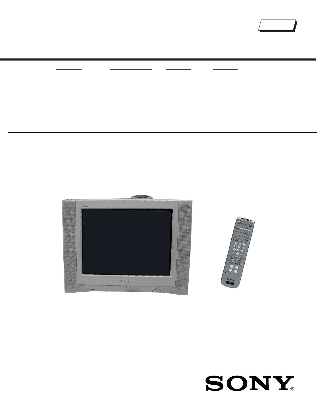
KV-21FA210
KV-21FA210
RM-Y180 LATIN NORTH SCC-S60P-A
RM-Y180 LATIN SOUTH SCC-S60Q-A
9-965-938-03
KV-21FA210 RM-Y180
TRINITRON® COLOR TELEVISION
Page 2

TABLE OF CONTENTS
SECTION TITLE PAGE
Specications ............................................................................................................................................................................. 4
Warnings and Cautions .............................................................................................................................................................. 5
Safety Check-Out ....................................................................................................................................................................... 6
Self-Diagnostic Function............................................................................................................................................................. 7
SECTION 1: DISASSEMBLY............................................................................................................................................................. 9
1-1. Rear Cover Removal.......................................................................................................................................................... 9
1-2. Chassis Assembly Removal............................................................................................................................................... 9
1-3. Service Position ................................................................................................................................................................. 9
1-4. Picture Tube Removal...................................................................................................................................................... 10
Anode Cap Removal Procedure....................................................................................................................................... 10
SECTION 2: SET-UP ADJUSTMENTS.............................................................................................................................................11
2-1. Beam Landing ...................................................................................................................................................................11
2-2. Convergence .................................................................................................................................................................... 12
2-3. Focus ............................................................................................................................................................................... 13
2-4. Screen (G2)...................................................................................................................................................................... 14
2-5. Method of Setting the Service Adjustment Mode ............................................................................................................. 14
2-6. White Balance Adjustments ............................................................................................................................................. 14
KV-21FA210
SECTION 3: SAFETY RELATED ADJUSTMENTS......................................................................................................................... 15
3-1. X R565 Conrmation Method (HV Hold-Down Conrmation) and Readjustments ........................................................ 15
3-2. B+ Voltage Conrmation and Adjustment ........................................................................................................................ 15
SECTION 4: CIRCUIT ADJUSTMENTS.......................................................................................................................................... 17
4-1. Setting the Service Adjustment Mode .............................................................................................................................. 17
4-2. Memory Write Conrmation Method ................................................................................................................................ 17
4-3. Remote Adjustment Buttons and IndicatorS .................................................................................................................... 17
4-4. ID Map Table.................................................................................................................................................................... 26
4-5. A Board Adjustments........................................................................................................................................................ 26
SECTION 5: DIAGRAMS................................................................................................................................................................. 29
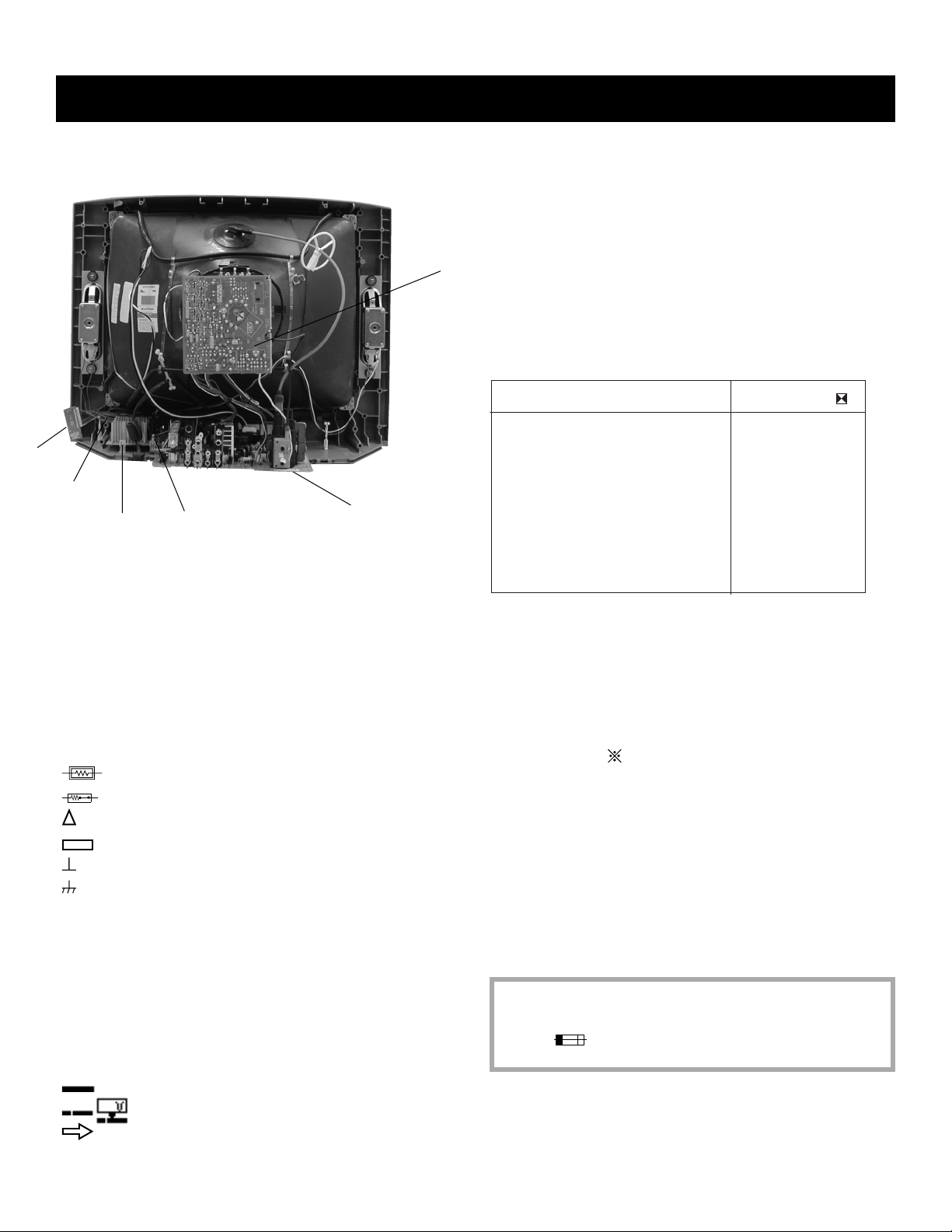
5-1. Circuit Boards Location .................................................................................................................................................... 29
5-2. Printed Wiring Board and Schematic Diagram Information.............................................................................................. 29
5.3 Block Diagram and Schematics ....................................................................................................................................... 30
A Board Schematic Diagram............................................................................................................................................ 31
M3 Board Schematic Diagram ......................................................................................................................................... 36
HR Board Schematic Diagram ......................................................................................................................................... 38
CV Board Schematic Diagram ......................................................................................................................................... 39
K Board Schematic Diagram............................................................................................................................................ 41
KB Board Schematic Diagram ......................................................................................................................................... 41
5-4. Semiconductors ............................................................................................................................................................... 42
SECTION 6: EXPLODED VIEWS.................................................................................................................................................... 43
6-1. Picture Tube ..................................................................................................................................................................... 43
6-2. Chassis ............................................................................................................................................................................ 44
SECTION 7: ELECTRICAL PARTS LIST ........................................................................................................................................ 45
— 3 —
Page 3
SPECIFICATIONS
KV-21FA210
Power requirements (Latin North) 120V, 60Hz
Power requirements (Latin South) 220V, 50/60Hz
Number of Inputs/Outputs
Video
1)
2
S Video
2)
1
Y, P
B
, P
R
3)
1
Audio
4)
2
Speaker output (W) 6 W x 2
External Subwoofer 14W
Headphones
5)
1
Power Consumption (W)
In use (Max) (Latin North) 145W
In use (Max) (Latin South) 140W
In Standby 1W
Dimensions(W/H/D)
mm 609 x 488 x 503 mm
in
24 x 19
1/4
x 20
Mass
kg 29 kg
lbs
63 lbs. 9 oz.
KV-21FA210
Television system
American TV Standard, NTSC
Channel coverage
VHF: 2-13/ UHF: 14-69/ CATV: 1-125
Picture tube
FD Trinitron® tube
Visible screen size
Actual screen size
20 inch picture measured diagonally
21 inch measured diagonally
— 4 —
1)
1 Vp-p 75 ohms unbalanced, sync negative
2)
Y: 1 Vp-p 75 ohms unbalanced, sync negative
C: 0.286 Vp-p (Burst signal), 75 ohms
3) Y: 1.0 Vp-p, 75 ohms, sync negative; PB: 0.7 Vp-p, 75 ohms;
PR Vp-p, 75 ohms.
4)
500 mVrms (100% modulation), Impedance: 47 kilohms
5)
More than 408 mVrms at the maximum volume setting (variable)
More than 408 mVrms (x); Impedance (output): 2 kilohms
Antenna
75 ohm external terminal for VHF/UHF
Supplied Accessories
Remote Commander:
RM-Y180
Size AA (R6) batteries (2)
Antenna, Telescopic
(•) SRS (SOUND RETRIEVAL SYSTEM)
The (•) SRS (SOUND RETRIEVAL SYSTEM) is manufactured by
Sony Corporation under license from SRS Labs, Inc. It is covered by U.S.
Patent No. 4,748,669. Other U.S. and foreign patents pending.
The word ‘SRS’ and the SRS symbol (•) are registered trademarks of
SRS Labs, Inc. BBE and BBE symbol are trademarks of BBE Sound, Inc.
and are licensed by BBE Sound, Inc. under U.S. Patent No. 4,638,258.
Design and specications are subject to change without notice.
Page 4

KV-21FA210
WARNINGS AND CAUTIONS
CAUTION
Short circuit the anode of the picture tube and the anode cap to the metal chassis, CRT shield, or carbon painted on the CRT, after
removing the anode.
WARNING!!
An isolation transformer should be used during any service to avoid possible shock hazard, because of live chassis. The chassis of
this receiver is directly connected to the AC power line.
! SAFETY-RELATED COMPONENT WARNING!!
Components identifi ed by shading and ! mark on the schematic diagrams, exploded views, and in the parts list are critical for safe
operation. Replace these components with Sony parts whose part numbers appear as shown in this manual or in supplements
published by Sony. Circuit adjustments that are critical for safe operation are identifi ed in this manual. Follow these procedures
whenever critical components are replaced or improper operation is suspected.
— 5 —
Page 5
SAFETY CHECK-OUT
KV-21FA210
After correcting the original service problem, perform the following
safety checks before releasing the set to the customer:
1. Check the area of your repair for unsoldered or poorly soldered
connections. Check the entire board surface for solder splashes and
bridges.
2. Check the interboard wiring to ensure that no wires are “pinched” or
touching high-wattage resistors.
3. Check that all control knobs, shields, covers, ground straps, and
mounting hardware have been replaced. Be absolutely certain that
you have replaced all the insulators.
4. Look for unauthorized replacement parts, particularly transistors,
that were installed during a previous repair. Point them out to the
customer and recommend their replacement.
5. Look for parts which, though functioning, show obvious signs of
deterioration. Point them out to the customer and recommend their
replacement.
6. Check the line cords for cracks and abrasion. Recommend the
replacement of any such line cord to the customer.
7. Check the B+ and HV to see if they are specifi ed values. Make sure
your instruments are accurate; be suspicious of your HV meter if sets
always have low HV.
8. Check the antenna terminals, metal trim, “metallized” knobs, screws,
and all other exposed metal parts for AC leakage. Check leakage as
described below.
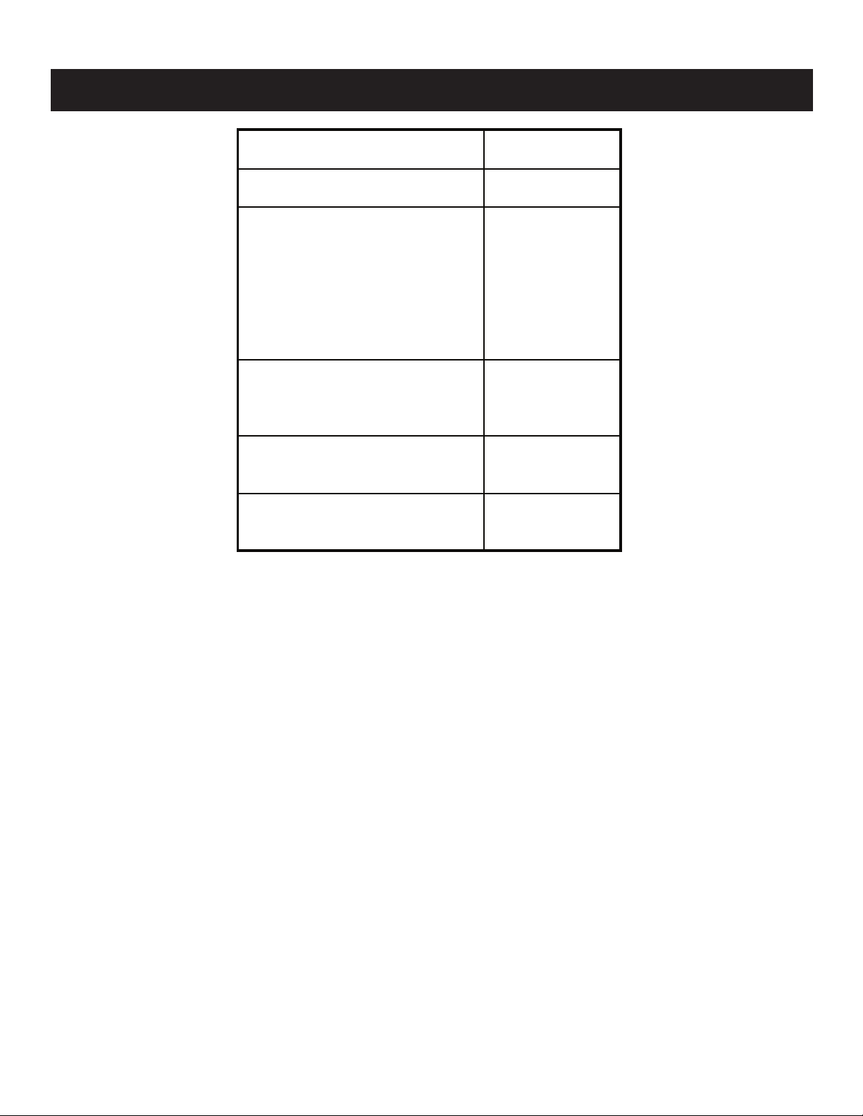
Leakage Test
The AC leakage from any exposed metal part to earth ground and
from all exposed metal parts to any exposed metal part having a
return to chassis, must not exceed 0.5 mA (500 microamperes).
Leakage current can be measured by any one of three methods.
1. A commercial leakage tester, such as the Simpson 229 or RCA
WT-540A. Follow the manufacturers’ instructions to use these
instructions.
2. A battery-operated AC milliampmeter. The Data Precision 245
digital multimeter is suitable for this job.
3. Measuring the voltage drop across a resistor by means of a VOM
or battery-operated AC voltmeter. The “limit” indication is 0.75
V, so analog meters must have an accurate low voltage scale.
The Simpson’s 250 and Sanwa SH-63TRD are examples of
passive VOMs that are suitable. Nearly all battery-operated digital
multimeters that have a 2 VAC range are suitable (see Figure A).
How to Find a Good Earth Ground
A cold-water pipe is a guaranteed earth ground; the cover-plate
retaining screw on most AC outlet boxes is also at earth ground. If the
retaining screw is to be used as your earth ground, verify that it is at
ground by measuring the resistance between it and a cold-water pipe
with an ohmmeter. The reading should be zero ohms.
If a cold-water pipe is not accessible, connect a 60- to 100-watt
trouble- light (not a neon lamp) between the hot side of the receptacle
and the retaining screw. Try both slots, if necessary, to locate the hot
side on the line; the lamp should light at normal brilliance if the screw
is at ground potential (see Figure B).
To Exposed Metal
Parts on Set
Trouble Light
Ohmmeter
Cold-water Pipe
0.15 F
1.5 K Ω
AC Outlet Box
AC
Voltmeter
(0.75 V)
Earth Ground
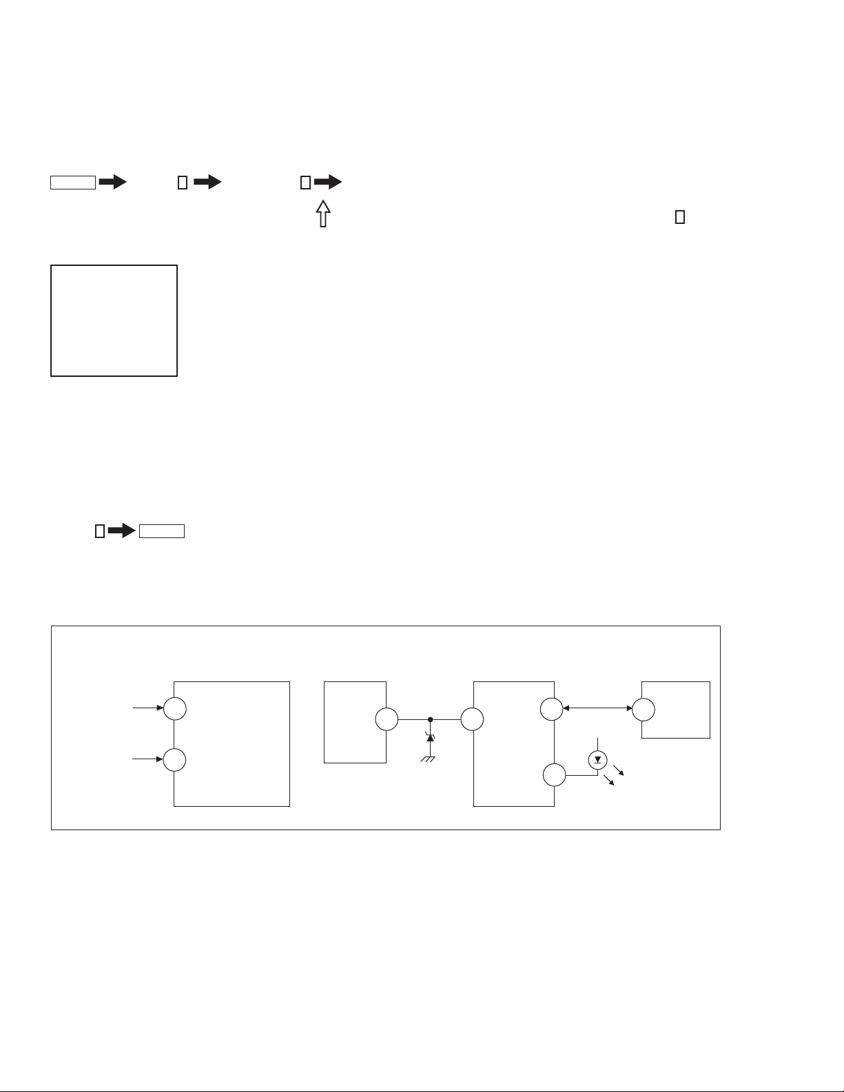
Figure A. Using an AC voltmeter to check AC leakage. Figure B. Checking for earth ground.
— 6 —
Page 6
KV-21FA210
Self Diagnosis
Supported model
2 times
4 times
5 times
LED ON 0.3 sec.
LED OFF 0.3 sec.
LED OFF
3 sec.
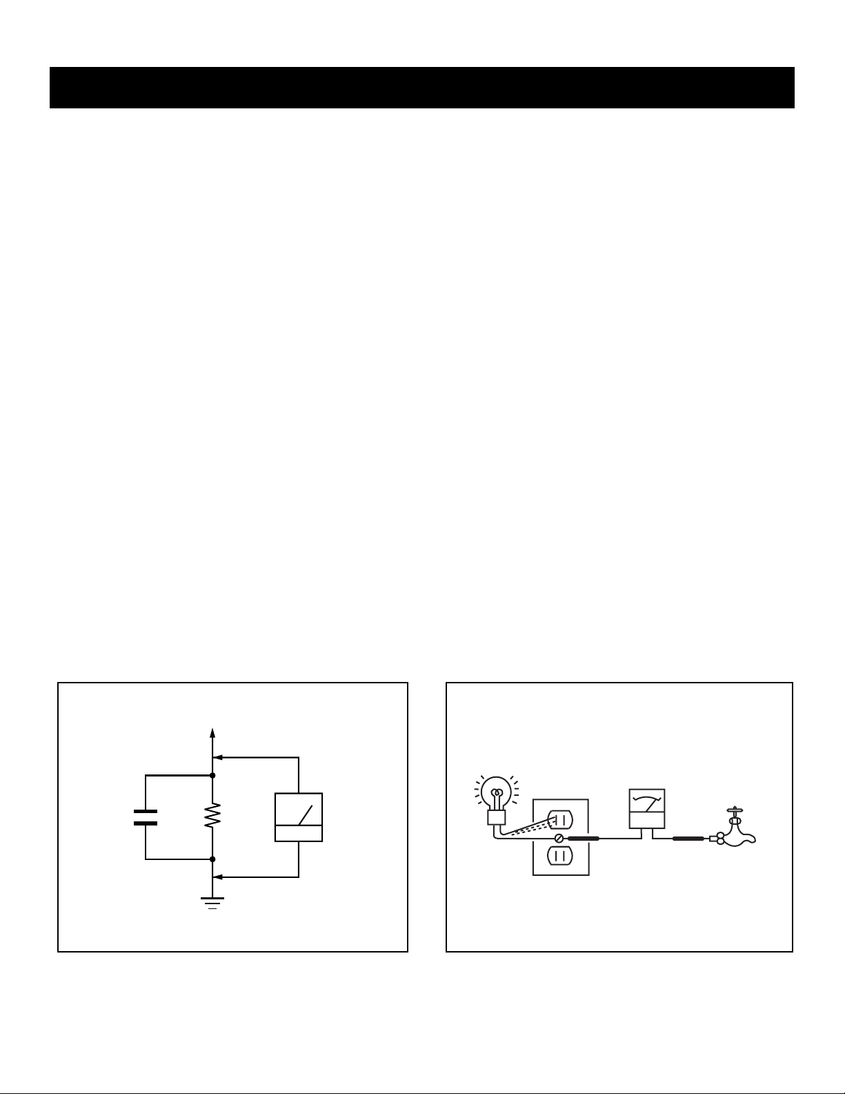
SELF-DIAGNOSTIC FUNCTION
The units in this manual contain a self-diagnostic function. If an error occurs, the STANDBY/TIMER LED will automatically begin to ash. The number
of times the LED ashes translates to a probable source of the problem. A denition of the STANDBY/TIMER LED ash indicators is listed in the
instruction manual for the user’s knowledge and reference. If an error symptom cannot be reproduced, the Remote Commander can be used to review
the failure occurrence data stored in memory to reveal past problems and how often these problems occur.
Diagnostic Test Indicators
When an error occurs, the STANDBY/TIMER LED will ash a set number of times to indicate the possible cause of the problem. If there is more than
one error, the LED will identify the rst of the problem areas.
Results for all of the following diagnostic items are displayed on screen. No error has occurred if the screen displays a “0”.
Diagnostic Item
Description
Power does not turn on
+B overcurrent (OCP)*
I-Prot
IK (AKB)
No. of times
STANDBY/ TIMER
lamp ashes
Does not light
2 times
4 times
5 times
Self-Diagnositc
Display/
Diagnostic Result
2:0 or 2:1
4:0 or 4:1
5:0 or 5:1
Probable Cause Location
• Power cord is not plugged in.
• Fuse is burned out (F601). (A Board)
• H.OUT (Q505) is shorted. (A Board)
• IC1751 is shorted. (CV Board)
• +13V is not supplied. (A Board)
• IC545 is faulty. (A Board)
• Video OUT (IC545) is faulty.
(A Board)
• IC001 is faulty. (A Board)
• Screen (G2) is improperly adjusted.**
Detected Symptoms
• Power does not come on.
• No power is supplied to the TV.
• AC Power supply is faulty.
• Power does not come on.
• Load on power line is shorted.
• Has entered standby state after horizontal raster.
• Vertical deection pulse is stopped.
• Power line is shorted or power supply is stopped.
• No raster is generated.
• CRT Cathode current detection reference pulse
output is small.
*If a +B overcurrent is detected, stoppage of the vertical deection is detected simultaneously. The symptom that is diagnosed rst by the
mircrocontroller is displayed on the screen.
**Refer to Screen (G2) Adjustments in Section 2-4. of this manual.
Display of Standby/Timer LED Flash Count
Diagnostic Item Flash Count*
+B Overcurrent 2 times
I-Prot 4 times
IK (AKB) 5 times
*One ash count is not used for self-diagnostic.
Stopping the Standby/Timer LED Flash
Turn off the power switch on the TV main unit or unplug the power cord from the outlet to stop the STANDBY/TIMER LAMP from ashing.
Standby/Timer LED
— 7 —
Page 7
KV-21FA210
A BOARD
IC001
Y/CHROMA JUNGLE
A BOARD
IC545
V. OUT
A BOARD
IC001
SYSTEM
A BOARD
IC002
MEMORY
IK-AKBIN
FROM
CV BOARD
IC1751 PIN 5
I-HLDWN
FROM
A BOARD
IC561
PIN 7
72
O-LED
REF
I-Prot
IO-BDAT
BDA
DISPLAY
51
3
78
79
53
5
Self-Diagnostic Screen Display
For errors with symptoms such as “power sometimes shuts off” or “screen sometimes goes out” that cannot be conrmed, it is possible to bring up past
occurrences of failure on the screen for conrmation.
To Bring Up Screen Test
In standby mode, press buttons on the Remote Commander sequentially, in rapid succession, as shown below:
Display
Self-Diagnostic Screen Display
Handling of Self-Diagnostic Screen Display
Since the diagnostic results displayed on the screen are not automatically cleared, always check the self-diagnostic screen during repairs. When you
have completed the repairs, clear the result display to “0”.
Unless the result display is cleared to “0”, the self-diagnostic function will not be able to detect subsequent faults after completion of the repairs.
Clearing the Result Display
To clear the result display to “0”, press buttons on the Remote Commander sequentially when the diagnostic screen is displayed, as shown below:
Channel 8
Quitting the Self-Diagnostic Screen
To quit the entire self-diagnostic screen, turn off the power switch on the Remote Commander or the main unit.
Channel
SELF DIAGNOSTIC
2: 000
3: N/A
4: 000
5: 001
101: N/A
ENTER
5
Sound Volume - Power ON
Note that this differs from entering the Service Mode (Sound Volume + ).
Numeral “0” means that no fault was detected.
Numeral “1” means a fault was detected one time only.
Self-Diagnostic Circuit
+B overcurrent (OCP)
Occurs when an overcurrent on the +B (135V) line is detected by pin 72 of IC001 (A Board). If the voltage of pin 72 of IC001 (A Board) is less than 1V
when V.SYNC is more than seven verticals in a period, the unit will automatically turn off.
I-Prot
Occurs when an absence of the vertical deection pulse is detected by pin 78 of IC001 (A Board). Power supply will shut down when waveform interval
exceeds 2 seconds.
IK (AKB)
If the RGB levels* do not balance within 2 seconds after the power is turned on, this error will be detected by IC001 (A Board). TV will stay on, but
there will be no picture.
*(Refers to the RGB levels of the AKB detection Ref pulse that detects 1K).
— 8 —
Page 8
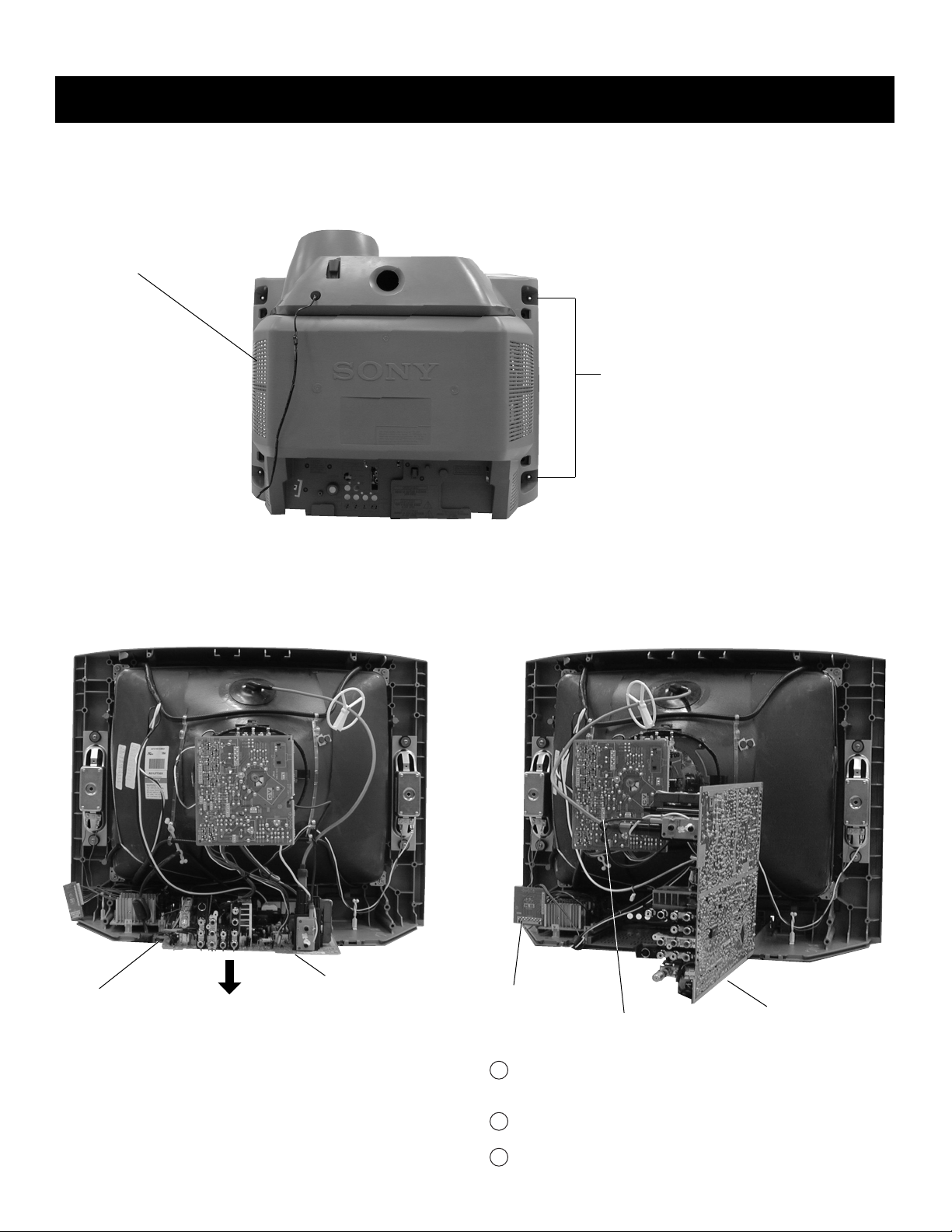
1-1. REAR COVER REMOVAL
Rear Cover
SECTION 1: DISASSEMBLY
6
Screws +BVTP 4X16 TYPE2 TT(B)
KV-21FA210
1-2. CHASSIS ASSEMBLY REMOVAL 1-3. SERVICE POSITION
Claw
Chassis Assembly
KB Board
CV Board
A Board
the way.
— 9 —
1
Unplug KB Board and 2 pin woofer connector and move out of
2
Press on catch tab to release A Board.
Disconnect remaining cables to allow A Board to be removed.
3
Page 9
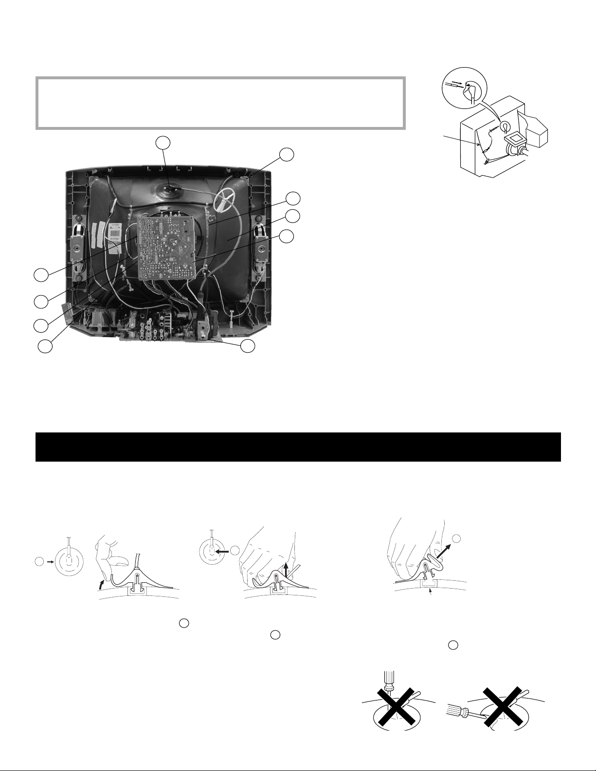
1-4. PICTURE TUBE REMOVAL
WARNING: BEFORE REMOVING THE ANODE CAP
High voltage remains in the CRT even after the power is disconnected. To avoid electric shock,
discharge CRT before attempting to remove the anode cap. Short between anode and CRT
coated earth ground strap.
1
10
1. Discharge the anode of the CRT and remove the anode cap.
8
7
3
6
2
5
9
4
2. Unplug all interconnecting leads from the defl ection yoke, neck
assembly, degaussing coils and CRT grounding strap.
3. Remove the CV Board from the CRT.
4. Remove the chassis assembly.
5. Loosen the neck assembly fi xing screw and remove.
6. Loosen the defl ection yoke fi xing screw and remove.
7. Place the set with the CRT face down on a cushion and remove
the degaussing coil holders.
8. Remove the degaussing coils.
9. Remove the CRT grounding strap and spring tension devices.
10. Unscrew the four CRT fi xing screws [located on each CRT
corner] and remove the CRT [Take care not to handle the CRT
by the neck].
KV-21FA210
Coated
Earth
Ground
Strap
ANODE CAP REMOVAL PROCEDURE
WARNING: High voltage remains in the CRT even after the power is disconnected. To avoid electric shock, discharge CRT before attempting to
remove the anode cap. Short between anode and coated earth ground strap of CRT.
NOTE: After removing the anode cap, short circuit the anode of the picture tube and the anode cap to either the metal chassis, CRT shield, or carbon
painted on the CRT.
REMOVAL PROCEDURES
c
b
a
Anode Button
Turn up one side of the rubber cap in
the direction indicated by arrow
a
.
HOW TO HANDLE AN ANODE CAP
1. Do not use sharp objects which may cause damage to the surface of the anode
cap.
2. To avoid damaging the anode cap, do not squeeze the rubber covering too
hard. A material fi tting called a shatter-hook terminal is built into the rubber.
3. Do not force turn the foot of the rubber cover. This may cause the shatter-hook
terminal to protrude and damage the rubber.
Use your thumb to pull the rubber
cap fi rmly in the direction indicated
by arrow
.
b
When one side of the rubber cap separates from
the anode button, the anode cap can be removed
by turning the rubber cap and pulling it in the
direction of arrow
.
c
— 10 —
Page 10
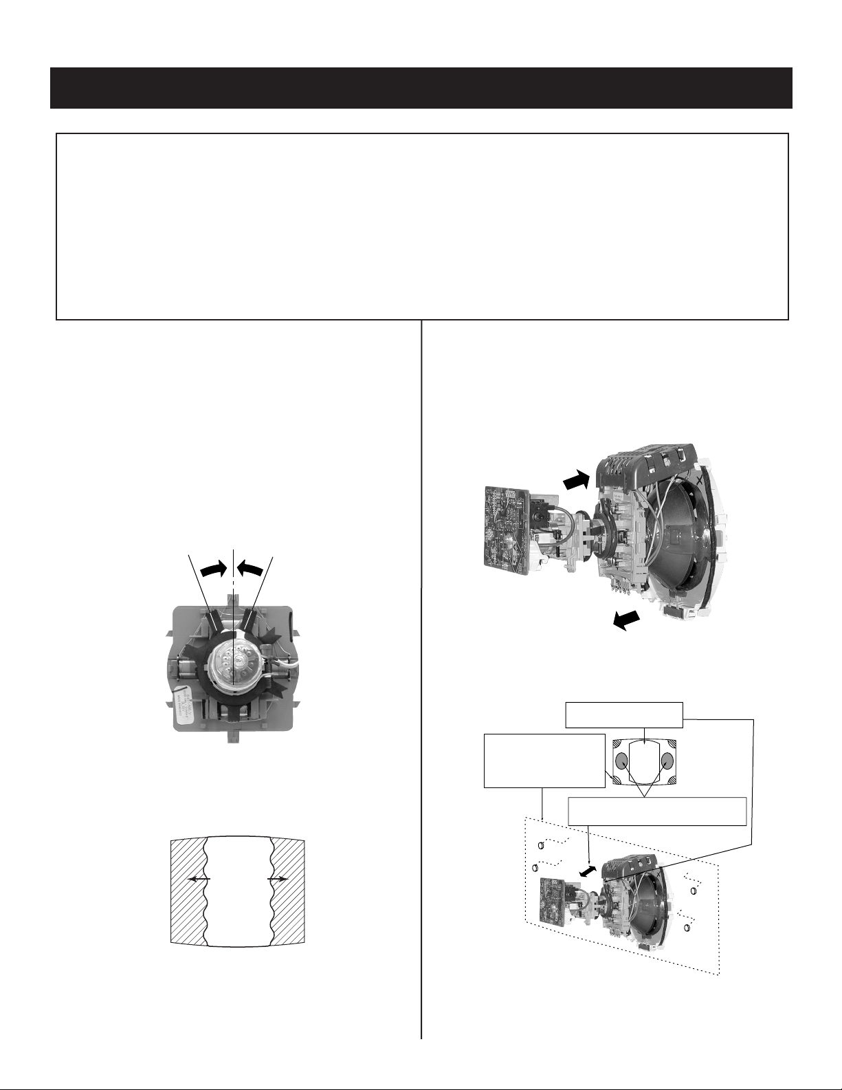
SECTION 2: SET-UP ADJUSTMENTS
Purity Control
a
c
b
d
b
a
c d
Purity control
corrects this area.
Disk magnets
or rotatable disk
magnets correct
these areas (a-d).
Deflection yoke positioning
corrects these areas.
KV-21FA210
The following adjustments should be made when a complete
realignment is required or a new picture tube is installed.
These adjustments should be performed with rated power supply
voltage unless otherwise noted.
Set the controls as follows unless otherwise noted:
VIDEO MODE: Standard
PICTURE CONTROL: Normal
BRIGHTNESS CONTROL: Normal
2-1. BEAM LANDING
Before beginning adjustment procedure:
1. Degauss the entire screen.
2. Feed in the white pattern signal.
ADJUSTMENT PROCEDURE
1. Input a raster signal with the pattern generator.
2. Loosen the deection yoke mounting screw, and set the purity
control to the center as shown below:
Perform the adjustments in order as follows:
1. Beam Landing
2. Convergence
3. Focus
4. Screen (G2)
5. White Balance
Note Test Equipment Required:
1. Color Bar Pattern Generator
2. Degausser
3. DC Power Supply
4. Digital Multimeter
6. Switch over the raster signal to red and blue and conrm the
condition.
7. When the position of the deection yoke is determined, tighten it with
the deection yoke mounting screw.
8. If landing at the corner is not right, adjust by using the disk magnets.
3. Turn the raster signal of the pattern generator to green.
4. Move the deection yoke backward, and adjust with the purity control
so that green is in the center and red and blue are even on both
sides.
5. Move the deection yoke forward, and adjust so that the entire
screen becomes green.
— 11 —
Page 11
KV-21FA210
B
G
R
Center dot
V.STAT magnet
RV1750
V.STAT
B
G
R
B
R
G
B
R
G
R G B
B G R
1
2
b
b
b
b
b
b
b
a
a
b
a
a
a
a
3
R
G
B
B
G
R
BMC MAGNET
PURITY
V.STAT
b
BMC magnet
a
2-2. CONVERGENCE
Before starting convergence adjustments:
1 Perform FOCUS, VLIN and VSIZE adjustments.
2. Set BRIGHTNESS control to minimum.
3. Feed in dot pattern.
VERTICAL STATIC CONVERGENCE
1. Adjust V. STAT magnet to converge red, green and blue dots in the
center of the screen (Vertical movement adjust S V.STAT RV1750 to
converge).
HORIZONTAL STATIC CONVERGENCE
If the blue dot does not converge with the red and green dots, peform
the following:
1. Move BMC magnet (a) to correct insufcient H.Static convergence.
2. Rotate BMC magnet (b) to correct insufcient V.Static convergence.
3. After adjusting the BMC magnet, repeat Beam Landing Adjustment.
2. Tilt the V. STAT magnet and adjust static convergence to open or
close the V. STAT magnet.
When the V. STAT magnet is moved in the direction of arrow a and b,
red, green, and blue dots move as shown below:
— 12 —
Page 12
DYNAMIC CONVERGENCE ADJUSTMENT
Before performing this adjustment, perform Horizontal and Vertical Static
Convergence Adjustment.
1. Slightly loosen defl ection yoke screw.
2. Remove defl ection yoke spacers.
3. Move the defl ection yoke for best convergence as
shown below:
G
B
R
R
G
B
BGR
B
G
R
R
B
G
R
B
G
KV-21FA210
B R R B
(R)(B) (B)(R)
4. Adjust XCV core to balance X axis.
5. Adjust YCH VR to balance Y axis.
6. Adjust vertical red and blue convergence with V.TILT (TLV VR.)
Note: Perform adjustment 3-6 while tracking items 1 and 2.
TLH+
TLH-
SCREEN-CORNER CONVERGENCE
BGR
B
G
R
B
G
R
B
R
G
B
R
G
R
GB
4. Tighten the defl ection yoke screw.
5. Install the defl ection yoke spacers.
TLH PLATE ADJUSTMENT
1. Input crosshatch pattern.
2. Adjust PICTURE QUALITY to standard, PICTURE and BRIGHTNESS
to 50%, and OTHER to standard.
3 Adjust the Horizontal Convergence of red and blue dots by tilting the
TLH plate on the defl ection yoke.
RV1750
V. STAT
TLH Plate
1. Affi x a permalloy assembly corresponding to the misconverged areas:
b
a
ba
a-d: screen-corner
misconvergence
c
d
c
d
2-3. FOCUS
1. Adjust FOCUS control for best pictures.
Focus (FV)
Screen (G2)
CV
Board
XCV
(TLV)
YCH
TLV
— 13 —
Page 13
KV-21FA210
2-4. SCREEN (G2)
1. Input a dot pattern.
2. Set the PICTURE and BRIGHTNESS controls at minimum and
COLOR control at normal.
3. Adjust SBRT, GCUT, BCUT in service mode with an oscilloscope as
shown below so that voltages on the red, green, and blue cathodes
are 160 ± 2VDC.
±
160 – 2VDC
Pedestal
Ground
4. Observe the screen and adjust SCREEN (G2) VR in FBT to obtain
the faintly visible background of dot signal.
2-5. METHOD OF SETTING THE SERVICE
ADJUSTMENT MODE
SERVICE MODE PROCEDURE
1. Standby mode (power off).
2. Press
Display
Channel 5 Sound Volume
on the Remote Commander (press each button within a second).
Power
+
2-6. WHITE BALANCE ADJUSTMENTS
1. Input an entire white signal with burst.
2. Set to Service Adjustment Mode.
3. Set the PICTURE and BRIGHTNESS to minimum.
4. Adjust with SBRT if necessary.
5. Select GCUT and BCUT with
6. Adjust with
3
and 6 for the best white balance.
7. Set the PICTURE and BRIGHTNESS to maximum.
8. Select GDRV and BDRV with
9. Adjust with
3
and 6 for the best white balance.
10. To write into memory, press
1
and 4 .
1
and 4.
MUTING
then
ENTER
.
SERVICE ADJUSTMENT MODE ON
1. The CRT displays the time being adjusted.
2. Press
3. Press
4. Press
Display
hsiz 16
to save into the memory.
service
ntsc
vchp
then
Category
defl
00000000
ENTER
Mode
Signal
Type
1
or 4 on the Remote Commander to select the time.
3
or 6 on the Remote Commander to change the data.
MUTING
Item
00000000
Display
Item
SERVICE ADJUSTMENT MODE MEMORY
Turn the set off then on to exit Service Adjustment Mode.
Signal
Type
Category
Mode
service defl hsiz 16
ntsc
vchp 00000000 00000000
Display
Item
write
Item
Data
MUTING
ENTER
Green
Red
— 14 —
Page 14
SECTION 3: SAFETY RELATED ADJUSTMENTS
KV-21FA210
3-1. X R565 CONFIRMATION METHOD
(HV HOLD-DOWN CONFIRMATION) AND
READJUSTMENTS
The following adjustments should always be performed when replacing
the following components which are marked with
diagram:
Part Replaced ( )
Y
DY, T585, CRT, IC001, IC561,
IC604, C507, C508, C506, T511,
Y
on the schematic
Adjustment ( )
HV HOLD-DOWN
R565
L510, C588, L588, C566, C561,
C563, D567, D568, D566,
PH602, R567, R568, R565,
R566, R562, R563, R561, R528,
R668....................A Board
PREPARATION BEFORE CONFIRMATION
1. Using a Variac, apply AC input voltage: 120 ±2 VAC.
2. Turn the POWER switch ON.
3. Input a white signal and set the PICTURE and BRIGHTNESS
controls to maximum.
4. Confi rm that the voltage between C566 (+) or TP30 and ground is
more than 105 VDC.
HOLD-DOWN OPERATION CONFIRMATION
1. Connect the current meter between Pin 11 of the FBT (T585) and the
PWB land where Pin 11 would normally attach (See Figure 1 on the
next page).
2. Input a dot signal and set PICTURE and BRIGHTNESS to minimum:
IABL = 100 ± 100µA.
3. Confi rm the voltage of A Board TP-23 is 138.0 ± 0.3VDC.
4. Connect the digital voltmeter and the DC power supply via Diode
1SS119 to C566 (+) and ground (See Figure 1 on next page).
5. Increase the DC power voltage gradually until the picture blanks out.
6. Turn DC power source off immediately.
7. Read the digital voltmeter indication (standard < 117VDC).
8. Input a white signal and set PICTURE and BRIGHTNESS to
maximum: IABL = 1650 ± 100µA.
9. Repeat steps 4 to 7.
HOLD-DOWN READJUSTMENT
If the setting indicated in Step 2 of Hold-Down Operation Confi rmation
cannot be met, readjustment should be performed by altering the
resistance value of R565 component marked with
X
.
T585
FBT
amPmeter
3.0 mA DC
range
ABL
+
-
A
IABL
3-2. B+ VOLTAGE CONFIRMATION AND
ADJUSTMENT
Note: The following adjustments should always be performed when
replacing the following components, which are marked with
schematic diagram on the A Board:
A BOARD: Y IC604, PH602
1. Using a Variac, apply AC input voltage: 130 + 2.0 / - 0.0 VAC.
2. Input a DOT pattern at Q.C.
3. Set the PICTURE and the BRIGHTNESS controls to minimum.
4. Confi rm the voltage of A Board between TP-23 & Ground is <136.6
VDC.
5. If step 4 is not satisfi ed, replace the components listed above, then
repeat Steps 1 – 3.
Y
on the
— 15 —
Page 15
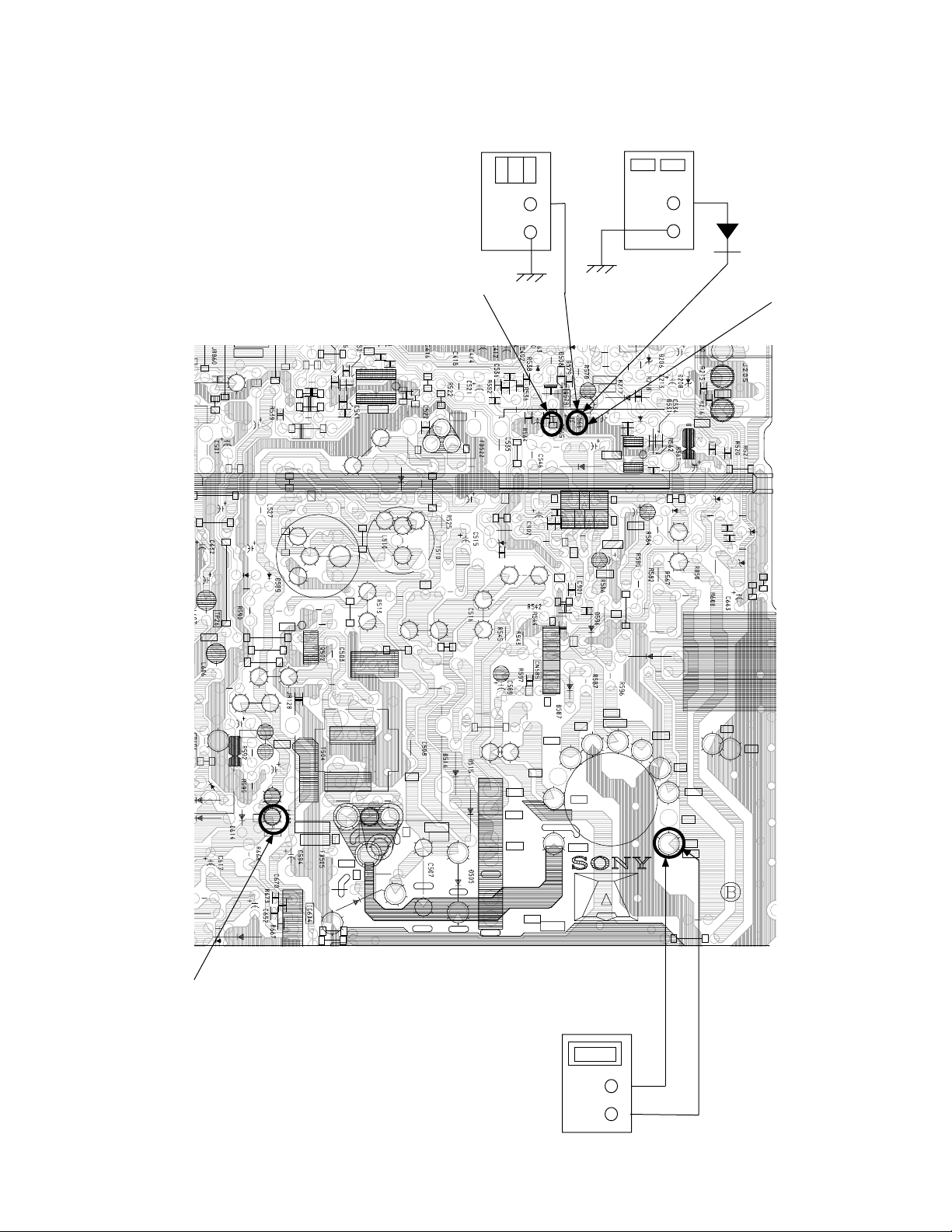
KV-21FA210
(
)
DIGITAL
MULTIMETER
+
-
X
R565
R
5
3
1
0
4
S
P
R
5
1
1
J
R
1
R
4
3
7
0
6
R
C
4
5
1
C
5
D
5
6
5
2
R
5
8
9
T
2
P
4
2
9
L
3
7
0
1
5
6
C
1
5
T
2
8
6
2
R
5
3
2
L
3
7
1
1
1
5
C
R
2
1
5
C
1
1
5
L
1
C
5
3
1
5
L
0
2
B
2
P
5
T
R
5
0
2
4
R
5
3
3
C
5
4
0
5
S
5
6
5
C
I
C
5
3
0
6
2
5
D
5
2
5
L
5
1
0
6
2
5
C
3
1
5
C
4
1
5
C
H
5
Q
B
5
2
5
C
L
5
1
5
R
5
3
7
R
5
6
2
2
R
5
5
2
2
E
C
5
2
7
R
5
4
9
R
5
1
5
6
7
C
5
6
1
R
5
4
6
5
4
5
D
6
R
5
4
8
C
5
4
5
R
9
0
R
5
4
0
0
0
D
2
7
C
R
5
4
7
6
6
1
5
L
R
5
C
5
4
8
1
J
R
5
0
POWER
SUPPLY
+
1SS119
C566
Q
4
0
2
R
4
0
8
R
4
1
1
.
H
P
O
R
T
R
P
0
T
3
6
6
5
D
R
5
2
9
C
5
6
2
C
5
2
9
1
6
5
C
I
C
5
4
4
2
C
5
9
7
1
T
P
V
.
O
U
T
5
4
7
5
4
5
C
I
4
1
C
5
9
5
P
7
T
1
R
9
0
1
5
1
2
C
2
5
2
8
D
5
2
8
D
6
1
R
5
8
3
2
8
5
C
P
T
3
3
Q
5
2
1
5
7
5
R
C
5
7
1
R
5
6
8
D
5
6
8
5
6
7
R
5
7
0
D
5
6
R
R
2
8
5
L
9
5
2
6
R
5
6
9
5
7
4
D
6
3
0
6
0
1
2
0
6
C
6
1
0
0
2
4
TP23
8
9
5
E
R
5
0
R
5
9
3
3
0
5
R
C
5
9
0
1
9
5
R
B
0
9
5
Q
R
5
9
4
T
P
1
3
4
2
6
E
C
6
C
P
3
T
2
1
6
8
C
4
0
4
2
6
D
4
5
0
5
C
H
-
O
Q
5
C
5
0
4
1
6
5
0
5
R
U
T
E
0
5
6
0
5
C
6
0
5
D
3
4
R
5
0
6
C
5
1
T
2
P
2
0
C
4
1
5
R
2
1
5
R
H
D
T
5
0
5
T
H
B
5
8
8
R
8
5
L
T
U
O
6
0
5
Q
6
G
2
0
0
V
8
N
/
C
V
D
Y
+
P
T
2
1
V
D
Y
-
T
2
P
7
H
D
Y
-
P
T
2
8
H
D
Y
-
H
D
Y
+
T
H
D
Y
+
3
1
H
-
O
2
P
9
1
5
5
N
C
D
R
5
9
8
T
1
P
9
H
E
A
T
E
R
N
D
5
V
U
T
-
1
3
V
G
G
N
D
G
N
D
N
D
5
5
T
+
1
3
V
N
/
C
A
B
L
T
2
P
0
R
5
8
8
F
B
T
1
AMMETER
3mA dc range
A
+
-
Figure 1
— 16 —
Page 16
service defl hsiz 16
ntsc
vchp 00000000 00000000
Category
Display
Item
Mode
Item
Data
Signal
Type
service defl hsiz 16
ntsc
vchp 00000000 00000000
Category
Display
Item
Mode
Item
Data
Signal
Type
write
service defl hsiz 16
ntsc
vchp 00000000 00000000
Category
Display
Item
Mode
Item
Data
Signal
Type
write
Carry out Step 1 when adjusting
IDs 0-7 and when replacing and
adjusting IC002
SECTION 4: CIRCUIT ADJUSTMENTS
ELECTRICAL ADJUSTMENTS BY REMOTE COMMANDER
Use the Remote Commander (RM-Y180) to perform the circuit adjustments in this section.
Test Equipment Required: 1. Pattern generator 2. Frequency counter 3. Digital multimeter 4. Audio oscillator
KV-21FA210
4-1. SETTING THE SERVICE ADJUSTMENT
MODE
1. Standby mode (Power off).
2. Press the following buttons on the remote commander within a
second of each other:
Display
Channel 5 Sound Volumne +
Power
SERVICE ADJUSTMENT MODE ON
1. The CRT displays the item being adjusted.
2. Press 1 or 4 on the Remote Commander to select the item.
3. Press 3 or 6 on the Remote Commander to change the data.
4. Press
MUTING
then
ENTER
to write into memory.
SERVICE ADJUSTMENT MODE MEMORY
1. Press 8 then
ENTER
on the Remote Commander to initialize.
4-2. MEMORY WRITE CONFIRMATION
METHOD
1. After adjustment, pull out the plug from the AC outlet, then replace
the plug in the AC outlet again.
2. Turn the power switch ON and set to Service Mode.
3. Call the adjusted items again to conrm they were adjusted.
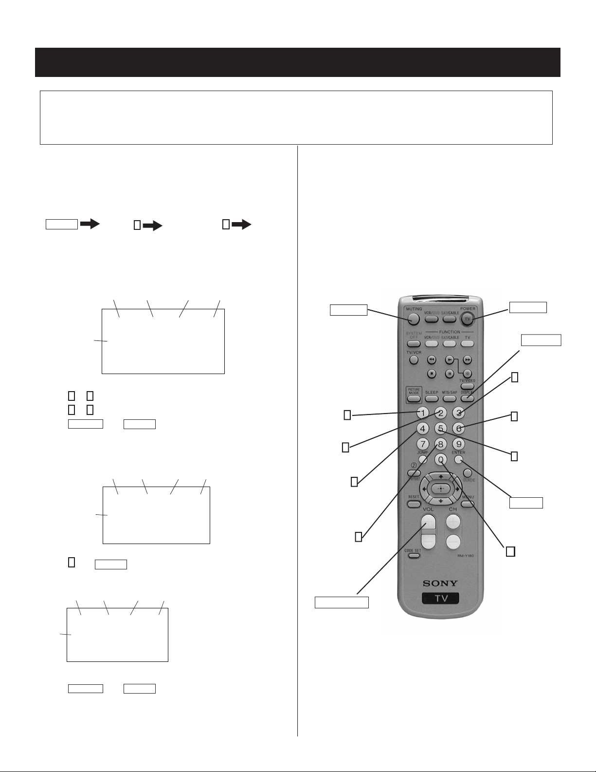
4-3. REMOTE ADJUSTMENT BUTTONS AND
INDICATORS
MUTING
(Enter into
memory)
1
Disp. (Item up)
2
(Device Item Up)
4
Disp. (Item down)
8
(Initialize)
POWER
(Service Mode)
DISPLAY
(Service Mode)
3
Item
(Data up)
6
Item
(Data down)
5
(Device item
down)
ENTER
(Enter into
memory)
0
(Remove from
memory)
3. Press
2. Turn set off then on to exit Service Adjustment Mode.
MUTING
then
ENTER
to write into memory.
VOLUME (+)
(Service Mode)
RM-Y180
— 17 —
Page 17
ADJUSTMENT ITEMS (1 OF 8)
DEVICE "DEF"
Item# OSD DETAIL
1 HSIZ H SIZE(EW DC) 00-63 25
2 HPOS H POSITION 00-63 41
3 VSIZ V RAMP SIZE 00-63 25
4 VPOS V POSITION(RAMP DC)not useful 00-63 34
5 VLIN V LINEARITY 00-63 36
6 SCOR S CORRECTION 00-63 39
7 VBOW BOW 00-63 36
8 VANG ANGLE 00-63 35
9 TRAP EW TRAPESIUM 00-63 29
10 PAMP EW PIN 00-63 39
11 UPIN UPPER PIN 00-63 28
12 LPIN LOWER PIN 00-63 29
13 TROT TROT 00-255 128
14 HBLK H BLK mode select 00-01 0
15 LBLK HBLK front timing 00-63 11
16 RBLK HBLK rear timing 00-15 35
17 VBLK V BLK width 00-03 0
18 HMSK TOP VEND(when MACROVISION)prevent OFF 00-01 0
19 HDW H PULSE WIDTH(25u/19u) 00-01 1
20 AFC AFC GAIN 00-01 0
21 AFC1 AFC1 TIME CONSTANT 00-07 3
22 AFCW AFC1 PULL IN WIDE 00-01 1
23 CDMD V DET WINDOW SW TIMING 00-03 1
24 HSS SYNC SLICE LEVEL(H sepa) 00-03 0
25 VSS SYNC SLICE LEVEL(V sepa) 00-03 3
26 SLDN Auto Slice level DOWN 00-03 0
27 SLUP Auto Slice level UP 00-01 0
28 JPSW Jump SW 00-01 0
29 HOSC H VCO fo ADJUST 00-255 5
30 EHT EHT 00-15 6
31 EHTG EHT MODE 00-01 0
Range
(DEC)
KV-21FA210
Initial Data
DEVICE "16:9"
Item# OSD DETAIL
1 PAMP EW PIN 00-63 59
2 UPIN UPPER PIN 00-63 15
3 LPIN LOWER PIN 00-63 21
4 ACLV ACL VTH 00-03 0
5 ABLV ABL VTH 63-00 58
DEVICE "VP1"
Item# OSD DETAIL
1 RDRV R DRIVE 00-127 55
2 GDRV G DRIVE when Color Temp. is "Cool" and "Neutral" 00-127 38
3 BDRV B DRIVE when Color Temp. is "Cool" and "Neutral" 00-127 47
4 RCUT 00-1023 130
5 GCUT 00-1023 90
6 BCUT 00-1023 72
7 SCON CONTRAST LEVEL 00-127 20
8 SHUE TINT 00-127 8
9 SCOL COLOR LEVEL 00-127 17
10 SBRT BRIGHT 00-255 40
11 RON R OUTPUT MUTE 00-01 1
12 GON G OUTPUT MUTE 00-01 1
13 BON B OUTPUT MUTE 00-01 1
14 BLLV BLUE STRETCH(00:no <-> 11:deep) 00-03 1
15 MTRX MATRIX RATIO SELECT 00-03 2
16 AXIS R-Y PHASE OFFSET 00-63 48
17 SSHO SHARPNESS GAIN(OVER) 00-63 17
18 SSHP SHARPNESS GAIN(PRE) 00-63 26
19 SHPF SHARPNESS fo(00:2 CLK <-> 11:5 CLK) 00-03 1
Range
(DEC)
Range
(DEC)
Initial Data
Initial Data
— 18 —
Page 18

ADJUSTMENT ITEMS (2 OF 8)
DEVICE "VP1"
Item# OSD DETAIL
20 SHCL SHARPNESS CPRING LEVEL 00-15 0
21 SHMX SHARPNESS LIMITER LEVEL 00-15 15
22 ACLV ACL VTH 00-03 0
23 ABLV ABL VTH 00-63 0
24 AKBD AKB Self Diagnostic Counter(@1sec) 00-07 0
25 AKBS AKB H/W S/W Switch 00-02 1
26 REFP AKB REFPLS timing 00-01 1
27 YNRC YNR LIMITER LEVEL 00-15 15
28 BKON BLACK STRETCH ON 00-01 1
29 BKTH BLACK STRETCH DETECTOR TRESH LEVEL 00-255 22
30 BKAR BLACK STRETCH DETECTOR TRESH AREA 00-03 1
31 BKSP BLACK STRETCH START POINT 00-03 3
DEVICE "VP2"
Item# OSD DETAIL
1 VMLO VM LEVEL at "Low" Setting 00-15 10
2 VMHI VM LEVEL at "High" Setting 00-15 15
3 VMDL VM DELAY 00-15 6
4 VMPL VM POLARITY 00-01 0
5 VMWD VM WIDTH 00-03 0
6 VMCL VM CORING LEVEL 00-15 0
7 VMMX VM LIMITER LEVEL 00-15 15
8 CKLV COLOR KILLER VTH 00-127 1/YUV:0
9 CKON FORCE KILLER 00-01 0
10 ALFA ADAPTIVE DET SENSITIVITY 00-03 2
11 YCMD YC SEPA FORCE SELECT(00:ADAPTIVE 01:H 10:V 11:HV) 00-03 0
12 VACL V APERTURE CORING LEVEL 00-15 0
13 VAGA V APERTURE GAIN LEVEL 00-15 Soft Cont'l
14 VAMX V APERTURE LIMITER LEVEL 00-15 3
15 GAMM GAMMA(00:no <-->11:deep) 00-03 Soft Cont'l
16 YDLY Y DELAY TIME 00-03 3/YUV:3
17 CDLY C DELAY 00-03 2/YUV:2
18 YOFF Y OUTPUT MUTE 00-01 0
19 CBPF C BPF fo HI 00-01 0/YUV:0
20 CLIM C OUTPUT LIMITER 00-15 15
21 YFSL Y BAND WIDTH 00-03 0
22 CFSL C BAND WIDTH 00-03 0
23 BGPP BGP(for C DECODER)TIMING 00-31 8
24 NRCH NOISE DET TIME CONSTANT 00-03 0
25 NRCL NOISE DET TIME CONSTANT 00-255 8
26 NRVL NOISE DET VTH 00-255 16
27 NRVH NOISE DET VTH 00-255 0
28 GDOF G DRIVE 00-31 18
29 BDOF B DRIVE 00-31 31
30 GCOF G CUTOFF 00-31 02
31 BCOF B CUTOFF 00-31 00
32 DCTV DCTRANSFER VTH 00-127 5
33 DCTG DCTRANSFER GAIN 00-31 Soft Cont'l
Range
(DEC)
Range
(DEC)
Initial Data
Initial Data
KV-21FA210
— 19 —
Page 19
ADJUSTMENT ITEMS (3 OF 8)
DEVICE "VIVID"
Item# OSD DETAIL
1 VPIC Picture(VIVID) 00-63 63
2 VBRI Brightness(VIVID) 00-63 31
3 VCOL Color(VIVID) 00-63 31
4 VHUE Hue(VIVID) 00-63 31
5 VSHA Sharpness(VIVID) 00-63 31
6 VVM VM(VIVID) 00-02 2
7 VTRI Color Temp(VIVID) 00-02 0
8 VAPA Aperture G(VIVID) 00-15 7
9 VGMA Gamma(VIVID) 00-03 3
10 DCTG DCT LV(VIVID) 00-03 16
DEVICE "STD"
Item# OSD DETAIL
1 VPIC Picture(STANDARD) 00-63 50
2 VBRI Brightness(STANDARD) 00-63 37
3 VCOL Color(STANDARD) 00-63 31
4 VHUE Hue(STANDARD) 00-63 31
5 VSHA Sharpness(STANDARD) 00-63 31
6 VVM VM(STANDARD) 00-02 1
7 VTRI Color Temp(STANDARD) 00-02 1
8 VAPA Aperture G(STANDARD) 00-15 7
9 VGMA Gamma(STANDARD) 00-03 3
10 DCTG DCT LV(STANDARD) 00-03 16
Range
(DEC)
Range
(DEC)
KV-21FA210
Initial Data
Initial Data
DEVICE "MOVIE"
Item# OSD DETAIL
1 VPIC Picture(MOVIE) 00-63 31
2 VBRI Brightness(MOVIE) 00-63 54
3 VCOL Color(MOVIE) 00-63 25
4 VHUE Hue(MOVIE) 00-63 31
5 VSHA Sharpness(MOVIE) 00-63 31
6 VVM VM(MOVIE) 00-02 0
7 VTRI Color Temp(MOVIE) 00-02 2
8 VAPA Aperture G(MOVIE) 00-15 7
9 VGMA Gamma(MOVIE) 00-03 3
10 DCTG DCT LV(MOVIE) 00-03 16
DEVICE "SPORTS"
Item# OSD DETAIL
1 VPIC Picture(SPORTS) 00-63 63
2 VBRI Brightness(SPORTS) 00-63 31
3 VCOL Color(SPORTS) 00-63 34
4 VHUE Hue(SPORTS) 00-63 31
5 VSHA Sharpness(SPORTS) 00-63 31
6 VVM VM(SPORTS) 00-02 2
7 VTRI Color Temp(SPORTS) 00-02 0
8 VAPA Aperture G(SPORTS) 00-15 7
9 VGMA Gamma(SPORTS) 00-03 3
10 DCTG DCT LV(SPORTS) 00-03 16
Range
(DEC)
Range
(DEC)
Initial Data
Initial Data
— 20 —
Page 20
ADJUSTMENT ITEMS (4 OF 8)
DEVICE "Y"
Item# OSD DETAIL
1 COFI 0:4 Line delays 1:2 Line delays 00-01 0
2 YNRS YNR ON 00-01 0
3 YTHR Y SIGNAL GENERATE from 2DYCS 00-01 0
4 Y2D Y SIGNAL GENERATE from 2DYCS 00-01 0
5 2DFX C SIGNAL GENERATE from H/V BPF only 00-01 1
6 CLPS Y CLAMP TIME CONSTANT 00-01 1
7 VLPF Y_LPF(ANALOG) fo Adjust 00-03 3
8 CLPF C_LPF(ANALOG) fo Adjust 00-03 3
9 BKHS BLACK STRETCH HYSTERESIS 00-31 1
10 BPFB YCS HBPF SELECT(BACK) 00-03 1
11 BPFF YCS HBPF SELECT(FRONT) 00-01 1
DEVICE "C"
Item# OSD DETAIL
1 FORG CHROMA DECODER PHASE SELECT 00-03 0
2 FSEL CHROMA DECODER CLK SELECT 00-01 0/YUV:0
3 ACTL ANALOG ACC AMP MAX GAIN 00-03 3
4 A1FL 00-255 34
5 A1FH 00-01 0
6 A1ON ANALOG ACC AMP ON LEVEL 00-127 12
7 MV MACROVISION(BURST) DET TRESH 00-15 0
8 MV1S MACROVISION(BURST) DET ON 00-01 1
9 MV2S MACROVISION(BURST) DET POSITION 00-01 1
10 ACCS ACC ON/OFF 00-01 0/YUV:1
11 KILS KILLER DET SELECT 00-01 0/YUV:1
12 AASL C DECODER TIME CONSTANT(32,16,8,1H) 00-03 3
13 BASL ACC TIME CONSTANT 00-03 0
14 ATIM ANALOG ACC HYSTERESIS SELECT 00-03 0
15 VMSK ACC V BLK OFF WIDTH 00-07 0
16 A3ON ACC MAX GAIN 00-01 0
17 INTE C DECODER INTEGRATOR ENABLE 00-01 0
18 SIN C DECODER PHASE V ENABLE 00-01 0
19 CKVT PLL STOP BURST LEVEL 00-03 1
20 XFFR VCXO FORCE FREERUN 00-01 0/YUV:1
21 ACCV C DECODER PHASE V ENABLE 00-01 1
22 BWSL KILLER DET SELECT 00-01 1/YUV:1
23 BWDT PLL KILLER VTH 00-03 0/YUV:3
24 A23E AMP2,3 ON/OFF ENABLE(0 FIX) 00-01 1
25 A2ON ABL VTH 00-127 12
26 A3ON ACL VTH 00-127 12
27 A2FL AMP2 OFF LEVEL lower 00-255 34
28 A2FH AMP2 OFF LEVEL upper 00-01 0
29 A3FL AMP3 OFF LEVEL lower 00-255 34
30 A3FH AMP3 OFF LEVEL upper 00-01 0
31 AXTH AXS HYS 00-63 30
32 ACTH ROM HYS 00-63 10
33 AVAV AVE SEL AV 00-03 3
34 B2TH B2COMP 00-127 0
ANALOG ACC hysteresis
Range
(DEC)
Range
(DEC)
Initial Data
Initial Data
KV-21FA210
— 21 —
Page 21

ADJUSTMENT ITEMS (5 OF 8)
DEVICE "RGB"
Item# OSD DETAIL
1 AMUT RGB POWER ON MUTE 00-01 0
2 PMUT RGB MUTE(EXCEPT OSD) 00-01 1
3 VBLK 00-01 0
4 CORL R CUTOFF lower 00-255 200
5 CORH R CUTOFF upper 00-01 0
6 COGL G CUTOFF lower when Color Temp. is "Cool" and "Neutral" 00-255 200
7 COGH G CUTOFF upper when Color Temp. is "Cool" and "Neutral" 00-01 0
8 COBL B CUTOFF lower when Color Temp. is "Cool" and "Neutral" 00-255 200
9 COBH B CUTOFF upper when Color Temp. is "Cool" and "Neutral" 00-01 0
10 ABLS ABL SELECT (ON:00, OFF:01) 00-01 0
11 ACLS ACL ON (ON:00, OFF:01) 00-01 1
12 ALSP ACL SPEED 00-03 1
13 ALRS ACL RECOVER SPEED 00-15 2
14 ALAS ACL ATTACK SPEED 00-15 9
15 ABLG ABL GAIN 00-15 15
16 ALS2 ACL ATTACK SPEED(2) 00-03 2
17 AKBS AKB MODE 00-01 1
18 AKBP AKB PULSE HEIGHT 00-63 55
19 OSDL OSD LIMIT SELECT 00-01 0
20 MPXS UV MULTIPLEX ON 00-01 0/YUV:0
21 CXUV YC/YUV SELECT 00-01 0/YUV:1
22 UVIN U/V INVERT 00-01 0/YUV:0
23 UVOS UV OFFSET CANCELER ON 00-01 0/YUV:0
24 ACL SOFT ACL CONTROL 00-63 63
25 HBLS H BLK OFF 00-01 0
26 VENS V-latch OFF 00-01 0
27 UOFS U IN OFFSET 00-15 4
28 VOFS V IN OFFSET 00-15 9
29 AABL ANALOG ABL THRESHOLD LEVEL CONTROL 00-15 0
30 AABG ANALOG ABL GAIN CONTROL 00-01 0
31 AALG ANALOG ACL GAIN CONTROL 00-01 0
32 AABS ANALOG ABL ON/OFF CONTROL (ON:01, OFF:00) 00-01 0
33 AALS ANALOG ACL ON/OFF CONTROL (ON:01, OFF:00) 00-01 1
Range
(DEC)
Initial Data
KV-21FA210
— 22 —
Page 22

ADJUSTMENT ITEMS (6 OF 8)
DEVICE "DEFD"
Item# OSD DETAIL
1 VSTP V OUTPUT STOP 00-01 0
2 HFFR AFC1 FORCE FREERUN 00-01 0
3 HFUP H FREERUN FREQUENCY UP(700Hz) 00-01 0
4 VPHA V PHASE(V POSITION ADJUST) 00-15 0
5 JSWW Jump Pulse Width 00-01 0
6 EWG EWV AD OUTPUT LEVEL(6db) 00-01 0
7 EWCL EW/VRAMP DA CLOCK SELECT 00-03 2/YUV:2
8 EWDI EW/VRAMP DA DITHER 00-01 0
9 XF0A VCXO FREERUN ADJUST 00-15 0
10 BGST BGP(for PLL) TIMING 00-63 17
11 SKWI Skew correcter reference phase 00-01 0/YUV:0
12 XPHA VCXO PHASE ADJUST 00-15 10
13 SKEW Skew corrector phase control 00-07 0/YUV:3
14 HRMP AFC2 TIME CONSTANT 00-03 0
15 RPLU REF PLL TIME CONSTANT 00-07 3
16 RPLB REF PLL TIME CONSTANT 00-01 1
17 XF0B VCXO Fo ADJUST 00-03 0
18 RPLS REF VCO FB LOOP SELECT 00-01 0
19 SSM SyncSepaMasking CONTROL 00-01 0
20 VSAG V-SAG prevent ON 00-01 0
21 AFC2 AFC2 GAIN CONTROL 00-03 0
22 VRFL V RAMP FILTER SWITCHING OFF 00-01 0
23 SSLP LPF pre SYNC SEPA ON/OFF 00-01 0
24 IMTS I.M. TEST 00-01 0
25 XPLU ACP TIME CONSTANT 00-01 1
26 8FSC 8fscCLK Skew OFF 00-01 1/YUV:1
27 4FS2 4fscCLK Skew OFF 00-01 1/YUV:1
28 EWVR DSDAC V RESET Enable 00-01 0
29 VLOF IIC V Latch OFF(for TEST) 00-01 0
30 1WIN FORCE 1Window 00-01 1
31 BGPC ANGLE Return current up 00-01 0
32 MHDL ANGLE Return current up timing 00-01 1
33 BFRE force V FREERUN 00-01 0
34 ANGG ANGLE Retun current up 00-01 1
35 ANGT ANGLE Retun current up timing 00-01 0
36 DOSD Digital OSD ON 00-01 0
37 ANGS AFC2 ANGLE/BOW INHIBIT 00-01 0
38 HRPP FRAMP RRAMP H OUT CONTROL RANGE 00-15 8
39 VF50 FORCE V FREERUN 50Hz 00-01 0
40 CLKS TBC clock system select 00-03 0
41 VBHK V BLK HALF KILL 00-01 0
42 DSYC CVBS INPUT CONTROL 00-01 0
43 VPW V Pulse Wide 00-01 1
44 QSW MODULATOR FEEDBACK GAIN CONTROL 00-01 0
45 ADTY CLOCK DUTY CONTROL at IIC QSWITCH=ON 00-01 0
46 DTH DITHER THRESHOLD LEVEL CONTROL at IIC AUTOD=ON 00-03 1
47 HBSW HBLK REFERENCE AFC1/AFC2 00-01 0
48 DSCS ǻȈDAC CLOCK ON/OFF CONTROL 00-01 0
Range
(DEC)
KV-21FA210
Initial Data
— 23 —
Page 23
ADJUSTMENT ITEMS (7 OF 8)
DEVICE "OTHER"
Item# OSD DETAIL
1 PCLP SYNC TIP/PEDESTAL CLAMP SELECT 00-01 0
2 VRT ADC REFERENCE (00:1.15Vpp 01:1.25Vpp 10:1.35Vpp 11:1.45Vpp) 00-03 1/YUV:1
3 AM INTERIGENT MONITOR OUTPUT SELECT(analog) 00-15 0
4 DME INTERIGENT MONITOR OUTPUT SELECT(digital) 00-01 0
5 DM INTERIGENT MONITOR OUTPUT SELECT(digital) 00-31 0
6 14HI 4fsc(Skew)CLK POLARITY 00-01 0
7 14HD 4fscCLK(Skew)CLK DELAY ADJUST 00-03 1
8 28I 8fscCLK POLARITY 00-01 1
9 28D 8fscCLK DELAY ADJUST 00-03 1
10 ADCD ADC CLK DELAY ADJUST 00-03 1/YUV:0
11 CLKS AD/LOGIC CLK SWAP 00-01 0/YUV:0
12 HDSL HD OUT(for MCU)SELECT 00-01 1
13 CPSL PLL CP LATCH ON 00-01 0
14 CPCL PLL CP LATCH CLOCK 00-01 0
15 CPCP PLL CP LATCH POLARTY 00-01 0
16 DUMY DUMMY 00-0F 1
DEVICE "OSD"
Item# OSD DETAIL
1 HT HALF TONE LEVEL 00-03 0
2 OSLR R OSD LEVEL 00-63 27
3 OSLG G OSD LEVEL 00-63 27
4 OSDC 00-03 0
5 OSDB B OSD LEVEL 00-63 27
Range
(DEC)
Range
(DEC)
Initial Data
Initial Data
KV-21FA210
DEVICE "S/W ADKB"
Item# OSD DETAIL
1 SRIL S/W AKB RED OUTPUT Lower 00-255 Soft Cont'l
2 SRIH S/W AKB RED OUTPUT Upper 00-01 Soft Cont'l
3 SGIL S/W AKB GREEN OUTPUT Lower 00-255 Soft Cont'l
4 SGIH S/W AKB GREEN OUTPUT Upper 00-01 Soft Cont'l
5 SBIL S/W AKB BLUE OUTPUT Lower 00-255 Soft Cont'l
6 SBIH S/W AKB BLUE OUTPUT Upper 00-01 Soft Cont'l
7 SLM1 S/W AKB LIMIT DATA 1 00-255 4
8 SLM2 S/W AKB LIMIT DATA 2 00-255 29
9 SLM3 S/W AKB LIMIT DATA 3 00-255 130
10 SAD1 S/W AKB ADD DATA 1 00-255 1
11 SAD2 S/W AKB ADD DATA 2 00-255 1
12 SBIT S/W AKB BIT SHIFT DATA 00-05 0
13 SNOP S/W AKB POWER ON NOP TIMER COUNTER DATA 00-FF 1
14 SERL S/W AKB BIT ERROR JUDGE LEVEL 01-80 124
15 SPWC S/W AKB ERROR JUDGE COUNTER DATA 01-FF 2
16 SLMC S/W AKB LIM2/LIM3 JUDGE COUNTER DATA 01-FF 10
17 SPWL S/W AKB POWER ON MUTE OFF JUDGE LEVEL 01-80 30
18 SPMT S/W AKB POWER ON MUTE EXIT TIMER DATA(@100ms) 00-FF 120
19 SEEP S/W AKB INITIAL DATA EEPROM WRITE TIMER(@1sec) 00-FF 20
Range
(DEC)
Initial Data
— 24 —
Page 24
ADJUSTMENT ITEMS (8 OF 8)
DEVICE "AUDIO PROCESSOR"
Item# OSD DETAIL
1 SBAL Sub Balance 00-07 4
2 SBAS Sub Bass 00-07 0
3 STRE Sub Treble 00-07 0
4 SRL Surround Level 00-01 0
5 BBOL Surround Off-BBE Low 00-15 5
6 BBOH Surround Off-BBE High 00-15 8
7 BBSL Simulate BBE Low 00-15 2
8 BBSH Simulate BBE High 00-15 5
9 BBGL WOW Game BBE Low 00-15 5
10 BBGH WOW Game BBE High 00-15 9
11 BBTL SRS BBE Low 00-15 3
12 BBTH SRS BBE High 00-15 5
13 VFIX Audio output fix data 00-255 240
14 AGCL AGC level 00-03 2
DEVICE "MICROPROCESSOR"
Item# OSD DETAIL
1 DISP OSD horizontal offset 00-127 53
2 CCHP Closed Caption Horizontal Position 00-7E 73
3 HRLW Low limit of H-pulse counting window (RF) 00-255 16
4 HRHG High limit of H-pulse counting window (RF) 00-255 64
5 HSLW Low limit of H-pulse counting window (S-Video) 00-255 16
6 HSHG High limit of H-pulse counting window (S-Video) 00-255 64
7 HSDT H-pulse Detection(S-Video) 00-255 8
Range
(DEC)
Range
(DEC)
KV-21FA210
Initial Data
Initial Data
DEVICE "FEATURE"
Item# OSD DETAIL
ID0 Language related 00-255
ID1Video related00-255
ID2 Audio related 00-255
ID3 Miscellaneous 00-255
ID4 Miscellaneous 00-255
ID5 Miscellaneous 00-255
ID6 Miscellaneous 00-255
ID7 Miscellaneous 00-255
Notes:
Range (DEC) shows the range of possible setting for each Adjustment Mode.
Initial Data shows the standard settings for each Adjustment Mode.
Signal
Type
Chip
Version
Range
(DEC)
ID
Mode
Function
Number
service id's id5 19
ntsc
00010011
M37280MK-00SP VERB.O
Initial Data
SEE ID MAP
SEE ID MAP
SEE ID MAP
SEE ID MAP
SEE ID MAP
SEE ID MAP
SEE ID MAP
SEE ID MAP
Data
— 25 —
Page 25
4-4. ID MAP TABLE
0RGHO 'HVWLQDWLRQ ,'2 ,' ,' ,' ,' ,' ,' ,'
.9)$ /$7,11257+
.9)$ /$7,16287+
4-5. A BOARD ADJUSTMENTS
H. FREQUENCY (FREE RUN) CHECK
1. Input a TV mode (RF) with no signal.
2. Connect a frequency counter to base of Q502
(TP-25 H. DRIVE) on the A Board.
3. Check H. Frequency for 15735 ± 200 Hz.
V. FREQUENCY (FREE RUN) CHECK
1. Select video 1 with no signal input.
2. Set the conditions for a standard setting.
3. Connect the frequency counter to TP-27 (V OUT) or CN515 pin
(V DY+) and ground on the A Board .
4. Check that V. Frequency shows 60 ± 4 Hz.
6
DRIVE (SCON)
1. Input a color-bar signal and set the level to 75%.
2. Set in Standard mode.
3. Activate the Service Adjustment Mode.
3
4. Set AALS, ABLS, GON and BON items. Using
the following values. Leave RON set to “1”.
Display
Mode
Category
Item
and
6
set each to
Item
Data
96 + 3Vpp
8. Reset AALS, ABLS, GON and BON values to “1”.
AALS: ON (1)
ABLS: ON (0)
R ON: ON (1)
G ON: ON (1)
B ON: ON (1)
9. Press
MUTING
then
ENTER
to save into the memory.
DISPLAY POSITION ADJUSTMENT (DISP)
1. Input a color-bar signal.
2. Set to Service Adjustment Mode.
3. Select DISP with
4. Adjust values of DISP with
5. Write to memory by pressing
6. Check to see if the text is displayed on the screen.
Signal
Type
1
and 4 .
3
and 6 to adjust characters to the center.
MUTING
then
ENTER
Display
Mode
Category
Item
service micro disp 48
ntsc
.
Item
Data
KV-21FA210
Signal
Type
AALS: OFF (0)
ABLS: OFF (1)
R ON: ON (1)
G ON: OFF (0)
B ON: OFF (0)
5. Connect an oscilloscope probe to CV Board, J1751Pin 12 (KR) (Red
Out) .
6. Select SCON with
7. Adjust the value of SCON with
service video rdrv
ntsc
vchp
1
and 4 .
00000000 00000000
3
and 6 for 96 ± 3Vpp.
26
vchp
00000000 00000000
SUB BRIGHT ADJUSTMENT (SBRT)
1. Input a monoscope signal.
2. Activate the Service Adjustment Mode.
3. Set the PICTURE and BRIGHTNESS to minimum.
4. Select the SBRT item with
5. Adjust the values of SBRT with
crosshatch.
6. Press
MUTING
then
1
and 4 .
ENTER
3
and 6 to obtain a faintly visible
to save into the memory.
SUB HUE, SUB COLOR ADJUSTMENT
(SHUE, SCOL)
1. Input color-bar signal at 75%.
2. Activate the Service Adjustment Mode.
3. Set (PIC) to Max and (COL) to 50%.
4. Connect an oscilloscope probe to CV Board, CN301Pin
1
5. Select the SHUE and SCOL item with
6. While showing the SHUE item, adjust the waveform with
until the second and third bars show the same level
(V2 = V3 < 0.15Vp-p). Set Sub Hue -2 Step.
and 4 .
4
Blue Out.
1
and 4
— 26 —
Page 26
KV-21FA210
7. While showing the SCOL item, adjust the waveform with
until the fi rst and fourth bars show the same level
(V1 = V4 < 0.15Vp-p). Set Sub Col +3 Step.
8. Press
MUTING
then
V2 V3
V1
ENTER
V4
to save into the memory.
3
V. SIZE ADJUSTMENT (VSIZ)
1. Input a crosshatch signal.
2. Activate the Service Adjustment Mode.
3. Select the VSIZ item with
4. Adjust value of VPOS with
5. Press
MUTING
then
1
and 4 .
1
and 4 for the best vertical center.
ENTER
to save into the memory.
V. CENTER ADJUSTMENT (VPOS)
and 6
H. SIZE ADJUSTMENT (HSIZ)
1. Input a monoscope signal.
2. Activate the Service Adjustment Mode.
1
3. Select HSIZ with
4. Adjust with
5. Press
MUTING
and 4 .
3
and 6 for the best horizontal size.
ENTER
then
to save into the memory.
V. LINEARITY (VLIN), V. CORRECTION
(SCOR), PIN AMP (PAMP), AND
HORIZONTAL TRAPEZOID (HTRP)
ADJUSTMENTS
1. Input a crosshatch signal.
2. Activate the Service Adjustment Mode.
3. Select VLIN, SCOR, PAMP, and HTRP with with
4. Adjust with
5. Press
3
and 6 for the best horizontal size.
MUTING
then
V LINEARITY (VLIN)
to save into the memory.
ENTER
1
and 4.
Perform this adjustment after performing H. Frequency
(Free Run) Check.
1. Input a crosshatch signal.
2. Activate the Service Adjustment Mode.
3. Select the VPOS item with
4. Adjust value of VPOS with
5. Press
MUTING
then
1
and 4 .
3
and 6 for the best vertical center.
ENTER
to save into the memory.
H. CENTER ADJUSTMENT (HPOS)
Perform this adjustment after performing H. Frequency
(Free Run) Check.
1. Input a crosshatch signal.
2. Activate the Service Adjustment Mode.
3. Select the HPOS item with
4. Adjust the value of HPOS with
5. Press
MUTING
then
1
ENTER
and 4 .
3
and 6 for the best horizontal center.
to save into the memory.
V CORRECTION (SCOR)
PIN AMP (PAMP)
HORIZONTAL TRAPEZOID (HTRP)
— 27 —
Page 27
V. ANGLE (VANG), V. BOW (VBOW), UPPER
PIN (UPIN) AND LOW PIN (LPIN)
ADJUSTMENTS
1. Input a crosshatch signal.
2. Activate the Service Adjustment Mode.
3. Select VANG, VBOW, UPIN, and LPIN with 1 and 4.
4. Adjust with
5. Press
3
and 6 for the best picture.
ENTER
MUTING
then
V ANGLE (VANG)
V BOW (VBOW)
UPPER PIN (UPIN)
to save into the memory.
KV-21FA210
LOW PIN (LPIN)
SERVICE ADJUSTMENT MODE MEMORY
ENTER
0
Item
then
7
.
Item
Data
Green
Red
ENTER
1. After completing all adjustments, press
Read From Memory
Display
Mode
Category
service defl vbow
Signal
Type
ntsc
vchp
00000000 00000000
0
— 28 —
Page 28
SECTION 5: DIAGRAMS
KV-21FA210
5-1. CIRCUIT BOARDS LOCATION
KB Board
HR Board
5-2. PRINTED WIRING BOARD AND
All capacitors are in µF unless otherwise noted. pF : µµF 50WV or less
are not indicated except for electrolytics and tantalums.
All electrolytics are in 50V unless otherwise specifi ed.
All resistors are in ohms. k=1000, M=1000k
Indication of resistance, which does not have one for rating electrical
power, is as follows: Pitch : 5mm Rating electrical power :
1
All variable and adjustable resistors have characteristic curve B, unless
otherwise noted.
Readings are taken with a color-bar signal input.
Readings are taken with a 10M digital multimeter.
Voltages are DC with respect to ground unless otherwise noted.
Voltage variations may be noted due to normal production tolerances.
All voltages are in V.
S : Measurement impossibillity.
Circled numbers are waveform references.
K Board
M3 Board
A Board
SCHEMATIC DIAGRAM INFORMATION
/
W in resistance, 1/
4
: nonfl ammable resistor.
: fusible resistor.
: internal component.
: panel designation and adjustment for repair.
: earth ground
: earth-chassis
: B+line.
: signal path. (RF)
W and 1/
10
W in chip resistance.
8
: B-line. (Actual measured value may be different).
CV Board
The components identifi ed by X in this basic schematic diagram have
been carefully factory-selected for each set in order to satisfy regulations
regarding X-ray radiation. Should replacement be necessary, replace
only with the value originally used.
When replacing components identifi ed by
Y
, make the necessary
adjustments as indicated. If the results do not meet the specifi ed value,
change the component identifi ed by
X
and repeat the adjustment until
the specifi ed value is achieved. (Refer to Section 3: Safety Related
Adjustments on Page 15.)
When replacing the parts listed in the table below, it is important to
perform the related adjustments.
Part Replaced ( )
Y
DY, T585, CRT, IC001, IC561,
IC604, C507, C508, C506, T511,
Adjustment ( )
HV HOLD-DOWN
R565
L510, C588, L588, C566, C561,
C563, D567, D568, D566,
PH602, R567, R568, R565,
R566, R562, R563, R561, R528,
R668....................A Board
REFERENCE INFORMATION
RESISTOR : RN METAL FILM
: RC SOLID
: FPRD NONFLAMMABLE CARBON
: FUSE NONFLAMMABLE FUSIBLE
: RW NONFLAMMABLE WIREWOUND
: RS NONFLAMMABLE METAL OXIDE
: RB NONFLAMMABLE CEMENT
: ADJUSTMENT RESISTOR
COIL : LF-8L MICRO INDUCTOR
CAPACITOR : TA TANTALUM
: PS STYROL
: PP POLYPROPYLENE
: PT MYLAR
: MPS METALIZED POLYESTER
: MPP METALIZED POLYPROPYLENE
: ALB BIPOLAR
: ALT HIGH TEMPERATURE
: ALR HIGH RIPPLE
The components identifi ed by shading and ! symbol are critical for safety. Replace
only with part number specifi ed.
The symbol indicates a fast operating fuse and is displayed on the component
side of the board. Replace only with fuse of the same rating as marked.
— 29 —
Page 29
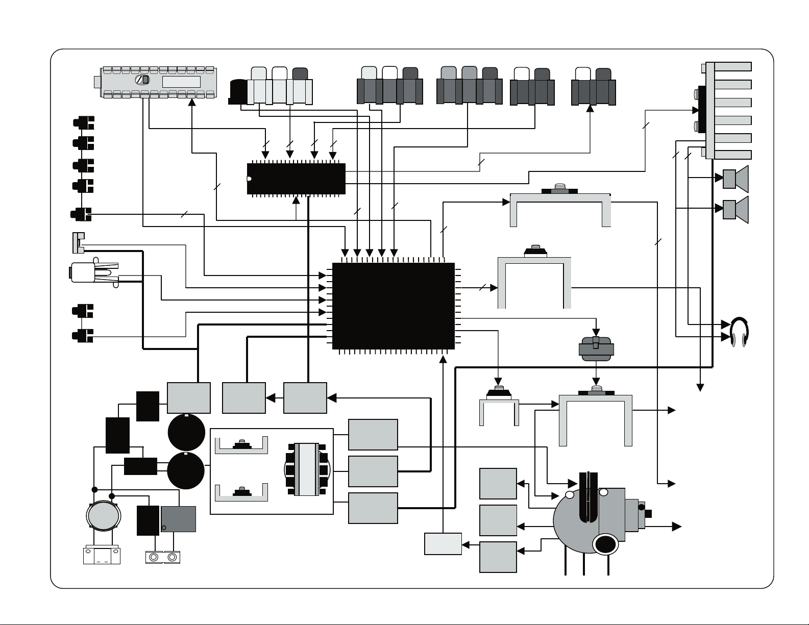
5.3 BLOCK DIAGRAM AND SCHEMATICS
5VDC
AudioProcessor
NJW1134
One-ChipIC
-Micro
YCJ
-3LCombFilter
RGB
KV-21FA210
— 30 —
Page 30
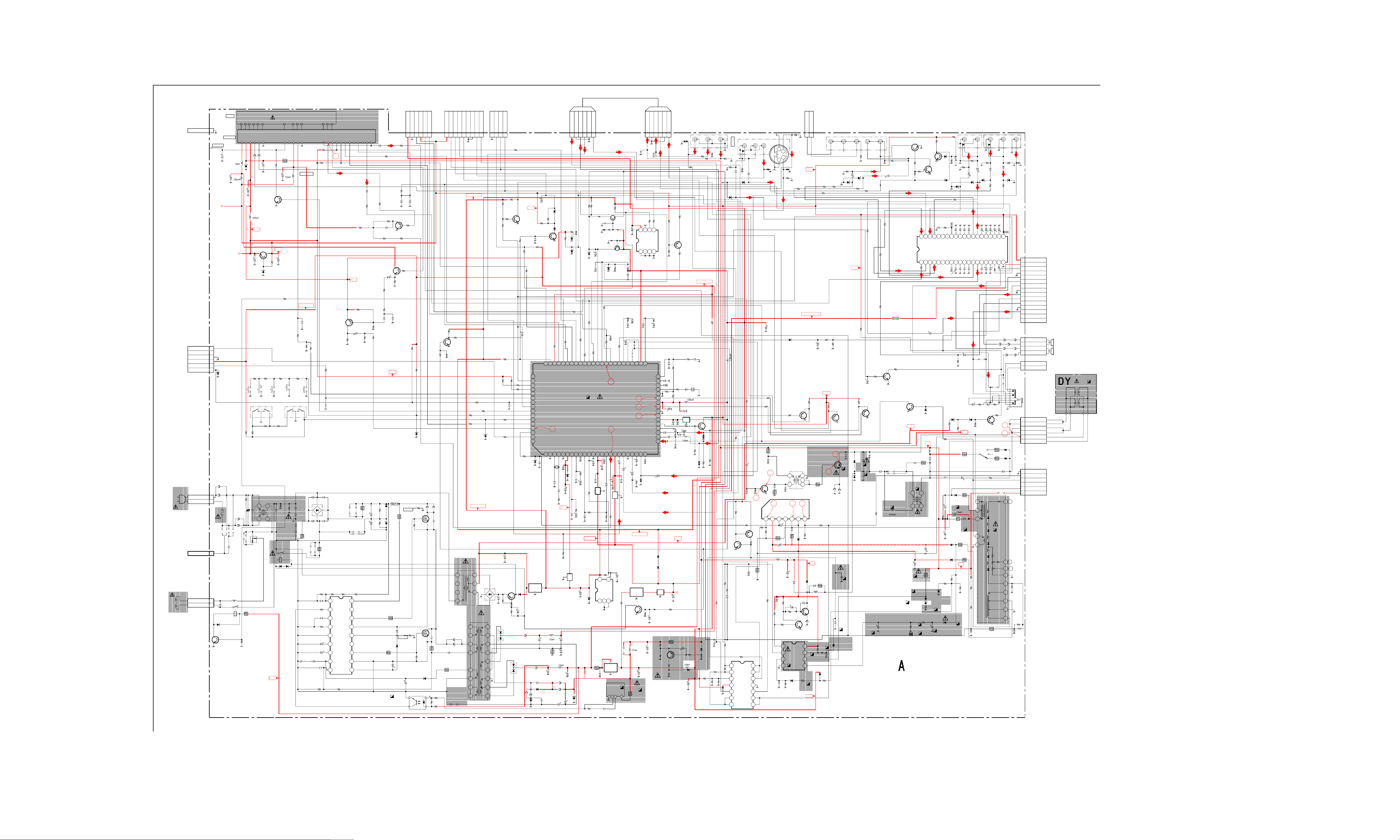
A BOARD SCHEMATIC DIAGRAM
1 | 2 | 3 | 4 | 5 | 6 | 7 | 8 | 9 | 10 | 11 | 12 | 13 | 14 | 15 | 16 | 17 | 18 | 19 | 20 | 21 | 22 |
KV-21FA210
A
—
B
—
C
—
D
—
E
—
F
—
G
—
H
—
I
—
J
—
K
—
L
—
M
—
N
—
O
TO M3 BOARD
T
T
C
U
G
O
A
T
D
F
N
R
V
A
G
F
9
TU101
T
C
U
G
O
A
F
R
R608
15k
3W
C663
R101
4.7
4.7k
50V
L010
C077
47
25V
Q009
2SD601A-QR
AGC
BTF-WA4
F
D
T
I
V
N
F
V
9
G
A
DET OUT
TP102
LIGHTENING
MONO
1
EY110
TP100
STEREO
6.3V
RF-AGC
C074
10
50V
C075
470
16V
TP602
9V
V
L
A
V
S
0
C
D
V
5
A
3
S
S
9
V
L
A
V
0
V
C
D
9
L101
L008
S
3
5
S
S
A
H
U
0
R107
0UH
8
0
1
R
D630
MTZJ-T-77-
30D
C076
100
25V
L009
+5V
LINE FILTER
*
4
1
*
2.2k
1/4W
S005
S007
R074
2.2k
1/4W
R650
680
1/4W
D650
MTZJ-T-77-
5.6C
FRONT_BUTTONS
T601
3
2
+9V
S004
R075
6.8k
1/4W
C603
MTZJ-T-77-
C660
MENU_BUTTONS
R067R069
820
1/4W
R603
*
RY600
AC POWER
D629
12B
47
25V
R033
220
STBY 5V
1/4W
C079
0.0047
50V
B
R102
R052
22k
1/10W
R699
*
C681
2200p
250V
C680
2200p
250V
D628
MA111-TX
C637
0.22
220
1/10W
R098
33k
R065
680
1/4W
S003
S002
S008
C613
0.0047
250V
F
C605
2200p
250V
C606
2200p
250V
0.0047
R602
*
JW618
C620
0.01
25V
16V
B
C636
0.22
16V
B
TP6035V
C661
100
25V
Q650
KSC2383-O
5V REG
TO HR BOARD
CN3001
CN002
6P
TIMER LED
1
MPWR LED
2
GND
3
STBY 5V
4
5
SIRCS
6
POWER ON
CN600
AC
2P
IN
AC IN
AC IN
EY111
LIGHTENING
CN501
2P
DGC
DGC
DGC
DGC
D003
MTZJ-T-77-
10B
FB671
1.1UH
FB672
1.1UH
2
1
F601
*
C601
MA111-TX
C523
*
D501
2SC3311A-Q
DGC DRIVER
*
L508
JW(5.0mm)
RY501
Q501
1
1
2
R071
6.8k
1/4W
S006
R073
1.5k
1/4W
R072
4.7k
1/4W
R600
0
0
2.2M
*
6
C602
R
1/2W
D
V
FB669
1.1UH
JW550
FB670
5.0MM
1.1UH
JW551
5.0MM
JW(7.5MM)
R507
1/10W
THP501
R508
10k
+9V
T
U
U
O
O
E
M
T
E
T
U
E
E
M
D
D
2
T
T
D
U
U
O
N
D
O
O
N
T
I
N
E
O
I
D
T
T
M
P
E
E
O
A
T
D
D
M
F
S
S
R109
4.7k
1
R111
4.7k
TV-VID
T
U
E
U
T
O
O
C
U
C
N
M
R
L
N
TV-R
C220
0.1
16V
R220
220
R323
560
1/4W
+5V
R083
150k 1/10W
Q005
2SB709A-QRS-TX
SYNC SEP
C054
1
50V
R081
R080
1/10W
R051
1k
1/4W
MAIN_PWR_BUTTON
C056
0.0022 50V B
C615
0.0047
250V
F
D605
GBJ4J10B9
C614
C619
0.0047
250V
250V
F
JW617
R601
*
R626
R627
9.1k
330k
1/10W
1/4W
1
B
VSENSE
R625
470
2
F/B
C633
0.001
50V
3
CT
R631
12k
4
RT
5
GND
C634
47
25V
6
TIMER
7
SS
C635
4.7
50V
8
VC1
9
OCP
C645
0.001
50V
B
R647
150 1/10W
R632
100
1/10W
47k
10k
1/10W
R687
**
R612
5
6
1
6
W
J
JW606
R629
330k
1/4W
8
VD
1
7
NC
1
6
VG(H)
1
5
VS
1
4
1
VB
3
NC
1
2
VG(L)
1
1
P-GND
1
0
VC2
1
1
6
W
J
JW605
5.0MM
5.0MM
R630
330k
1/4W
MCZ3001D
SW REG CON
IC600
470k
1/2W
C629
470
250V
C621
470
250V
CN302
C200
0.1
TV-L
16V
R032
220
R105
0
R322
470 1/10W
C312
220p
50V
CH
0
JR315
C051
10
50V
R086
1k
1/10W
R085
0
R084
680
1/10W
C053
0.047
16V
B
R082
1M
1/10W
R063
4.7k
1/10W
+5V
D613
*
R628
D612
470k
*
1/2W
R658
10
1/4W
C643
0.1
100V
R659
10
1/4W
C647
47
25V
PHOTOCOUPLER
6P
V
3
.
3
6
R200
220
R103
10k
1/10W
C080 C081
0.33
10V
B
Q306
2SB709A-QRS-TX
BUFFER
R321
100
1/4W
0
JR316
Q004
2SD601A-QRS-TX
BUFFER
R087
100
1/4W
C052
220p
50V
CH
R050
4.7k
1/4W
R112
4.7k
1/4W
D004
MTZJ-T-77-
10B
R615
0.1
1/2W
HS600
R640
1k
1/4W
R660
10k
1/10W
R651
100k
HS601
D618
UF4005PKG2
3
C642
220
50V
PH602
PC123FY2
3
4
CN10
D
N
G
5
0.33
10V
SW REG OUT
SW REG OUT
CN301
R670
10k
D631
V
9
3
1k 1/10W
9P
N
I
L
B
D
A
H
2
1
R055
4.7k
1/10W
Q006
2SD601A-QR
HP PROT
R056
10k
1/10W
FB617
FB616
1.1UH
1.1UH
C648
470p
1kV
S
C649
S
470p
1kV
R671
0.1
2W
R617
R616
1k 1/10W
2
1
R618
JW(5.0MM)
T
U
O
D
H
4
B
R652
100k
Q600
2SK2640
Q601
2SK2640
1/10W
TO CV BOARD
CN1752
CN003 CN200
E
N
I
L
V
9
1
D
S
N
/
K
B
G
G
N
I
2
4
3
5
6
D
D
N
M
N
G
V
R
G
8
7
1
9
STBY 5V
R054
22k
1/4W
R096
4.7k
1/10W
R053
22k 1/4W
R058
10k 1/4W
R057
1k 1/4W
R060
220 1/4W
D005
MTZJ-T-77-
10B
STBY 5V
T602
*
1
7
2
8
D2SB60A-F04
3
9
4
1
FB615
JW(5.0MM)
JW(5.0MM)
C672
22000p
800V
R619
0.47
1/4W
C630
470p
250V
B
3
2
FB618
4
6
7
8
C631
9
470p
250V
B
C611
470
50V
T603
18
17
16
15
14
13
12
11
10
4P 6P
T
K
T
FOR JIG
N
L
A
I
C
D
-
-
-
B
B
B
2
3
4
R029
220
1/4W
R092
R090
2.2k
22k
1/10W
1/10W
R091
47k
1/10W
R076
Q008
100
2SD601A-QRS-TX
1/4W
BUFFER
R555
1/10W
R037
10k
1/10W
R048
4.7k
1/10W
R047
R049
220
4.7k
1/4W
1/10W
R110
220
1/4W
C057
0.1
16V
B
1k 1/4W
R059
R062
470
1/4W
MTZJ-T-77-
C609
1000
25V
D608
D620
1SS119
R605
R606
10k
10k
R607
C612
1M
2.2
Q604
MSB709-RT1
12V REG
D615
FB606
MA7D50
JW(5.0MM)
D621
D5LC20U
FB604
0UH
10k
1/10W
R061
10k
1/4W
D006
5.1C
+9V
R035
100
R030
220
1/4W
C049
1
50V
65
66
67
68
69
70
71
72
73
74
75
76
77
78
79
80
IO
NJM2930F05
STBY 5V REG
IC LINK
C610
330p
500V
EL1Z-V1
C048
100
25V
R038
1k
1/10W
R039
330
1/10W
C047
470p
50V
CH
Q002
2SD601A-QR
R093
CONVERGENCE
47k
1/10W
T
S
N
N
I
-
B
O
I
O-HSYNC
O-RELAY
O-SEL1
O-SEL0
I-AFT
I-SIRCS
I-PWR
I-HLDWN
O-AGCMUTE
I-KEY
I-MENU
O-MONO
I-HSYNC
I-PROT
O-LED
O-MAGABASS
S
C
S
N
V
1 2 3 4 5 6 7 8 9
X001
C064
0.047
16V
B
C003
22p
50V
CH
G
IC608
C650
L606
1000
25V
R620
2.2
1W
C616
FB605
2200
D611
EL1Z-V1
FB602
0UH
C640
D624
330p
500V
D
D
1
N
N
U
V
Y
V
G
G
3
5
4
1
V-IN
IR_SENSOR
D558
MA111-TX
D559
R041
MA111-TX
4.7k
1/10W
R040
4.7k
1/10W
D045
MTZJ-T-77-
10B
R551
JW(7.5MM)
R031
220
)
M
1/10W
M
5
.
7
(
W
J
4
3
0
R
P
L
P
C
E
A
O
A
G
T
S
V
S
D
U
-
-
-
M
O
O
I
O
O
7
U
V
C
5
M
T
T
-
-
U
L
N
C
S
O
I
I
C
S
F
-
-
V
V
X
X
7
7
B
2
-
6
0
T
.
0
-
5
D
J
Z
T
C005
M
0.0022
50V
B
C009
C004
47p
50V
R002
25V
C618
220p
50VCH1
C006
CH
1000
25V
0
+5V
C007
470p
50V
CH
C008
R301
75
L002
I
M
E
C023
470
16V
C651
1000
25V
C625
10
50V
L607
C632
47
50V
FB603
0UH
FB601
0UH
C617
220
D614
100V
EZ0150AV1
220 100V
6
2
N
Y-IN
I
U
R045
R027
4.7k
1/10W
C390
0.01
25V
D390
MA111-TX
50V
CH
R095
0
W
4
/
1
0
2
2
0
7
0
R
T
T
A
A
D
D
B
S
-
O
O
I
I
IC001
V
3
G
.
I
3
D
-
-
C
S
S
C
E
S
V
R
V
C012
0.0047
50V
B
C090
0.01
25V
B
R006
4.7k
1/10W
CH
PST9143NL
STBY 5V RESET
R609
6.8
10W
R390
0
B
R393
2.2k
1/10W
C509
22
25V
N
I
L
C
A
L
B
A
R
E
T
L
I
F
_
T
C
D
C091
25V
C116
0.1
16V
I
M
E
L003
R116
470k
1/10W
1/10W
1 2 3
IC003
NJM2395F09
C690
0.01
25V
B
C652
0.022
25V
B
1/10W
560
1/10W
D351
MTZJ-T-77-
3.3B
1/10W
0.001 50V B
1k 1/10W
T
N
U
I
O
B
-
K
H
A
K
I
T
U
O
O
E
D
I
V
R
O
T
I
N
O
M
47
B
R015
10k
IC603
9V REG
IO
ERROR AMP
R044
4.7k
R862
220
C537
R553
22
6
N
I
V
T
N
I
A
M
V
0
5
1
4
1
0
C
C
3
1
3
0
.
1
5
0
V
45
G
47k
D044
MTZJ-T-77-
10B
D509
MTZJ-T-77-
3.3B
C351
470p
0
4
9
0
W
R
4
/
1
0
2
2
8
2
0
R
K
L
O
K
C
E
L
S
R
C
-
E
B
O
T
-
S
O
I
M65582MF-100FP
MICRO/Y-C-J/COMB
T
D
N
E
L
I
F
O
-
L
H
V
H
V
C
10 11 12 13 14 15 16 17 18 19 20 21 22 23 24
C011
0.001
50V
B
R004
470
1/10W
C010
50V
R115
470
R003
1/10W
1k
1/10W
C115
560p
50V
0.1
50V
D052
MTZJ-T-77-
5.6B
TP601
12V
R667
10k
1/10W
N
I
P
B
F
IC604
DM-58
VID-1
2SD601A
D
I
V
V
JR317
CN201
6P
D
D
1
N
N
Y
U
V
1
V-IN
C361
C360
220p
220p
V
G
G
5
6
3
2
4
D235
RD9.1EW-T1
U
I
N
VID-1
Y-IN
REARVIDEO1
VIDEO 1 VIDEO 2 VIDEO 3
S
V
I
D
J206
Y-IN
U-IN
R360
100
R361
0
JR314
3P
R306
R307
75
75
V-IN
100
R203
100k
MTZJ-T-77-
R202
100k
C203
0.1
16V
D200
D201
9.1B
R
S VIDEO
C202
0.1
16V
RD9.1ES-T1B2
V
L
J200
VID-1
4P
D232
RD9.1EW-T1
V1-L
V1-R
R314
10k
0.0033
R372
3.3k
1/10W
C094
0.01
25V
C100
0.1 50V
D050
D051
R591
R313
1/10W
0
Q301
2SB709A
IK BUFF
R312
R311
6.8k
220
1/10W
1/10W
STBY 5V
R036
2.2k
C325
50V
B
R371
1/10W
C328
0.01
25V
R337
C330
1/10W
0.01
25V
R370
2.2k
1/10W
C097
47
25V
C095
47 25V
B
C306
0.1
16V
C305
0.1
16V
C326
R324
0.22
2.7k
16V
1/10W
B
7
0
0
1M
C337
22p
22
X301
50V
CH
L006
C096
Q300
0.01
2SD601A-Q
25V
VM OUT
B
L005
EMI
R308
1k
L360
V-IN
C363
0.001
D234
L361
RD9.1EW-T1
C362
0.001
RD9.1EW-T1
U-IN
R309
10k
R310
1k
D236
R305
75
L
JW(10.0MM)
1/10W
JR313
0
VID-2
C502
330p
50V
R573
4.7k
1/10W
R540
10k
1/4W
Q573
2SB709A
SW
+5V+3.3V
R537
TP604
3.3V
C665
100
25V
R614
2.2k
1/10W
0.47 2W
C590
10 50V
R590
10k
1/4W
Q590
KTA1279
PROTECT
L609
D562
1SS133T-77
C520
22
50V
680k
)
M
M
0
.
5
(
W
J
1
1
5
R
R851
1k
1/10W
7
7
-
9
T
8
3
5
C542
3
D
1
0.0022
S
S
50V
1
B
R589
470k
1/4W
R535
2.2k
R534
15k
R533
2.7k
R530
10k
R852
10k
C539
0.01
25V
B
R572
4.7k
1/10W
Q572
2SD601A
SW
C534
0.0022
50V
B
R536
10k
C536
0.001
R557
2.2k
1/10W
R539
0
1
2
F
F
2
U
E
B
T
3
-
5
E
M
6
V
2
5
I
0
C
4
R
9
I
D
2
M
T
J
5
R
N
E
V
6
7
1/10W
R501
R317
220
1/10W
R560
1k
R503
4.7k
3W
J
W
(
C503
C
5
5
.
0.047
0
0
1
m
200V
m
)
Q502
2SC3209
H-DRIVE
R502
4.7k
1/4W
8
B
R541
15k
1/4W
R543
1.5
1/4W
R532
JW(5.0MM)
4
1
3
1
2
1
1
1
0
1
9
8
C099
47
25V
R315
220
E
V
I
R
D
1 2 3 4 5 6 7
R542
10k
1/4W
C041
10
50V
R394
10k
1/10W
V
5
C553
0.1 16V B
C552
10 50V
C370
0.0068
25V
O
P
C
M
V
A
H
R
V
+
D
V
C
Y
N
-
I
D
N
C
G
C302
0.1
L004
C019
0.1
50V
R352
470k
1/10W
C554
0.01
25V
JR44
0
P
M
A
R
V
D
V
N
I
1
O
E
D
I
V
C303
0.1
50V
R043
220
1/10W
IC002
M24C16-MN6T(A)
MEMORY
1 2 3 4
B
C033
0.01
414243444546474849505152535455565758596061626364
1
C
C
V
P
F
3
M
A
.
A
3
R
-
C
V
C
V
XTAL-PAL-N
XTAL-PAL-M
XTAL-NTSC
GND-DEF
5
VCC-3.3V
4
GND-OUT
3
VCC-3.3V
VM-OUT
N
I
2
O
E
D
B
T
I
R
R
V
V
V
RD9.1EW-T1
R303
75
1/10W
R042
220
1/10W
5678
R524
6.8k
1/10W
C551
1
50V
25V
B
40
APC
39
38
37
36
35
B-OUT
34
33
G-OUT
32
31
R-OUT
30
29
28
VZOUT
27
V-IN
C307
0.1
26
U-IN
16V
25
Y-IN
Y-IN
C021
0.1
16V
B
C304
0.1
50V
D230
VID-1
C-IN
Q390
2SD601A
SW
R391R392
4.7k
1/10W
Q391
SW
R351
10k
1/10W
C098
0.01
25V
B
R527
2.2k
1/10W
W
0
1
0
/
5
1
5
R
0
7
4
C
T
U
W
O
E
W
E
V
3
.
3
N
-
I
C
-
C
Y
V
C301
0.1
T
C
0
9
2
4
7
C015
2
5
0.1
V
16V
B
I
M
E
0
Y-IN
STBY 5V
1SS133T-77
1SS133T-77
IC633
C022
10
LF33CV
50V
3.3V REG
IO
G
R634
22
3W
Q608
2SD2144S
RELAY-DRIVE
L608
JW630
R668
1.2k
1/4W
145 3
FL001
EMI
R680
0
C600
R604
10
1k
50V
1/10W
R594
1k
C624
1/4W
10
160V
R595
470k
1/4W
R592
100k
1/4W
C638
100
25V
R593
10k
1/4W
9
C504
5.6K
1/4W
12
1
2
C505
680p
500V
820P 500V B
IC545
AN5522
VOUT
+
C
C
V
C545
R545
470
2W
C544
L527
JW(5.0mm)
C571
100
25V
R520
10k
1/10W
R575
1/4W
C529
0.0022
50V
TO K BOARD
B
R504
F
E
R
220 50V
47 50V
C527
22
160V
4.7
CH
3
4
R227
MA111-TX
1/10W
1
2
3
4
CN4002
75
C-IN
D410
R319
220
1/10W
C
C
V
R546
2.2
1/4W
C526
220p
500V
R521
680
1SS133T-77
R529
CN403
2P
RD9.1EW-T1
W
S
Y-IN
D231
RD9.1EW-T1
T505
134
13
T
U
O
C546
0.47
50V
B
C521 C522
50V
R522
330
1/4W
Q521
2SC3311A
PIN DRIVE
2
E
T
-
1
M
6
3
5
0
C
9
I
2
M
J
N
D528
22k
-
+
O
O
W
W
S
S
1
D237
+9V
R415
0
AUDIO OUT VAR/FIX
2
J205
4P
R201
100
R215
100k
D206
HZS9.1NB2
R218
0
R416
220
220 1/4W
R222
LINE A
C212
4.7
D208
LINE B
HZS9.1NB2
R217
JW68
220
MA111-TX
1K
Q400
2SD601A
MUTE
R216
100k
C213
4.7
D413
R402
V1-L
R479
1/10W
Q412
2SD601A-QR
MUTE
R406
220
1/10W
R407
220
1/10W
0
1k
2SD601A-QR
MTZJ-T-77-
Q401
MUTE
HZS9.1NB2
R212
R477
680
1/10W
D414
7.5B
D412
0
D205
220 1/4W
J202
C470
2P
470
YUV-R
16V
R213
R210
100k
100k
R478
10k
1/10W
C207
4.7
D204
HZS9.1NB2
YUV-L
V2-R
C206
4.7
RD9.1ES-T1B2
R
L
VID-2
MTZJ-T-77-
V
R226
75
R206
1/10W
100k
D202
9.1B
J201
3P
R207
100k
C204
0.1
C205
16V
0.1
16V
D203
V2-L
R208
R209
220
220
1/4W
1/4W
LINE B
C406
C410
C400
T
V
R211
220
1/4W
R250
0
NJW1134AGK1-TE2
AUDIO PROCESSOR
R221
220
1/4W
+9V
V1-R
V
L
IC400
B
1
N
I
A
1
N
I
1 2 3 4 5 6 7 8 9
R482
0
TV-R
R251
0
0.0082
2
0.33
-
10V
L
R400
4.7k
B
B
B
B
4
5
2
3
N
N
N
N
I
I
I
I
A
A
A
A
2
A
3
6
4
N
5
N
N
N
I
N
I
I
I
I
R
V
U
Y
LINE A
AUDIO VCC
PS401
R463
47k
0-VOL
R498
C499
0
4.7
1/4W
R499
10k
R494
10k
1/10W
C498
1
2SD601A
50V
+9V
D505
2kV 8200p
RGP15GPKG23
R316
2.2k
1/10W
2SB709A
BUFFER
BY228/A52A /
C507
1.2kV
C508
0.047
630V
D506
R549
Q305
C510
0.001
2kV
*
R320
2.2k
1/10W
2SB709A
BUFFER
2SD2627LS-YB11
R318
2.2k
1/10W
Q303
H-OUT
Q304
2SB709A
BUFFER
11
Q506
C506
0.001
10
R505
5
JW(5.0MM)
6
14
+
T
E
S
V
O
I
O
R
B
D
R548
15k
1/4W
R547
10k
1/4W
D545
GP08DPKG23
FB506
1.1UH
FB505
1.1UH
B+
D526
R525
C525
PG104R
1
L
R
T
N
C
D
L
O
H
V
47
2200p
1W
500V
L525
8mH
100p
500V
B
Q522
KTC4370A
PIN OUT
FB522
1.1UH
8
R561
10k
1/10W
7
6
5
D525
1SS133T-77
R563
10k
1/10W
C563
0.01
25V
B
JW(5.0MM)
D563
R562
10k
1/4W
C562
220
25V
C561
4.7
50V
5MM
JW491
10K
1/10W
Q411
MUTE
2SD601A
C458
JW (5.0mm)
Q578
SW
D508
MA111-TX
+5V
R578
B+
10k
1/4W
L513
10mH
R510
C512
0.001
C597
220
25V
MTZJ-T-77-
100V
D568
8.2B
C511
0.82
JW510
250V
5.0MM
JW519
7.5MM
L510
1
1SS133T-77
R565
10k
1/10W
C513
220
0.047
1/2W
200V
2.2mH
T511
2
345
R597
220k
1/10W
C595
220
25V
R567
47k
1W
D567
R566
100k
1/4W
GP08DPKG23
GP08DPKG23
1/10W
D569
MTZJ-T-77-
5.1C
R568
620
1/4W
C566
4.7
160V
TUNING CONTROL
Y/C/J
C408
C404
0.0015
0.0033
25V
2
L
B
6
N
I
C401
0.022
25V
0.0033
B
H
I
B
B
B
F
E
N
1
2
N
S
O
R
O
E
E
M
T
S
B
B
B
B
A
1
H
L
-
I
A
A
F
E
1
2
S
A
N
S
E
E
O
N
/
B
B
T
O
S
B
B
R
M
S
10 11 12 13 14 15 16 17 18 19 20
C403
C405
C407
0.033
0.0015
L
R-OUT
C457
JW (5.0mm)
R461
100k
C441
330
25V
D438
MTZJ-T-77-
MA111-TX
R438
R437
1k
4.7k
1/4W
1/10W
+9V
R513
220
3W
C515
4.7
250V
L515
D587
PG104R
R587
C589
47
22
1/4W
100V
L588
C588
R588
0.0047
22
200V
2W
C594
33
160V
R596
0.47
1/4W
D596
R598
0.47
1/4W
D598
B+
R850
R570
1/4W
R574
10k
EGP20DPKG2 3
18k
10k
1/4W
R569
10k
1/4W
R585
22k
D566
D435
0.033
C402
C416
C412
R
L
B
T
U
O
A
T
U
O
C411
0.33
10V
L-OUT
JW402
220 1/4W
R435
10k
1/10W
1
4
2
HEATER
6
5
C418 C420
C414
1
1
4.7 1
2.2
R
S
C
C
G
A
C413
SW515
H
T
C
1
C440
2SB709A
C422
1
9V
2122232425262728293031323334353637383940
L
F
S
+
T
E
B
V
C
R
C
V
L
B
A
C
A
D
V
D
S
V
N
C
S
C
G
100
R401 R403
C415
100
1
R
R-OUT
FB461
1.1UH
FB463
1.1UH
FB464
FB466
FB465
1.1UH
1.1UH
FB467
1.1UH 1.1UH
L-OUT
3
0
4
W
JW401
J
R440
220
330
1/4W
25V
Q435
MUTE
R514
R515
100
R583
0.47
1/4W
68
3W
0.56 250V
2W
T585
R512
FBT
R436
68
3W
GP08DPKG23
GP08DPKG23
C514
JW585
US
HEAD PHONE
0
15
16
D515
D514
5.0MM
HV
HV
FV
FOC
SV
G2
13
11
10
9
8
7
C582
0.068
200V
FB462
1.1UH
JW(7.5MM)
1.1UH
FB468
J401
JW(5.0mm)
TO KB BOARD
CN4010
CN404
15P
1
9V
2
AUDIO VCC
3
SP L+
4
GND-2
5
SP L-
6
STBY
7
IN L
8
GND
9
IN R
10
MUTE
11
SP R-
12
GND-2
13
SP R+
14
NC
15
NC
CN401
4P
SP R+
1
SP R-
2
SP L-
3
SP L+
4
1
HPSW1
2
HPSW2
TO K BOARD
CN4001
CN402
2P
CN515
6P
1
HDY+
HDY+
2
3
HDY-
4
HDYVDY-
5
VDY+
6
CN585
6P
1
GND
2
VD+
HEATER
3
NC
4
200V
5
6
+B
TO CV BOARD
CN1751
R581
100k
1/4W
R582
L582
H.DY H.DY V.DY V.DY
0.22
16V
B
B
L
E
E
N
N
I
O
T
L
A
L
-
A
E
E
N
N
O
I
T
L
C409
0.22
16V
R441
10B
R584
22k
1/4W
R586
2.2k
POWER SUPPLY
R528
6.8k
R526
22k
1/10W
+9V
TUNER/IF
DEFLECTION
AUDIO
MTS
9-965-938-01<BA6>A
— 31 —
Page 31

[POWER SUPPLY, DEFLECTION, TUNER/IF, AUDIO, MTS, TUNING CONTROL, Y-C JUNGLE] (COMPONENT SIDE)
A
G
1
C
6
TV/VIDEO
A
S
0
0
6
8
2
3
4
5
7
R
0
MENU/SEL
P
G
R065
E
7
Y
0
D
0
4
R069
C
6
6
0
R
D003
D
0
0
1
4
C
4
0
0
S
7
0
4
3
7
S
0
0
8
R
0
7
R
E
S
S
U
I
E
D
A
6
R602
R067
JW130
C
6
1
3
R071
C
6
0
5
6
R
0
3
6
9
9
R
0
0
5
R112
J
C
6
0
6
3
J
W
C
0
N
2
0
6
2
J
W
0
4
R
4
0
1
J401
4
J
W
0
3
2
J
W
5
4
J
W
0
1
5
J
W
8
C304
J
W
D230
FB461
JW402
J201
J
W
1
2
D203
FB462
D202
L
+
L
C
R
-
R
+
VOL- VOL+ CH- CH+ POWER
S
0
0
B
S
0
0
7
S
0
0
S
0
C
0
6
S
0
1
0
IC004
D
5
E
F
UP/DOWN
R
0
H
I
23456789101112
F
B
6
1
5
JW636
0
0
Q
-
2
6
-
A
1
2
1
Y
5
E
2
2
D
6
1
3
2
C
9
6
JW131
E
4
3
Y
C
6
1
4
E
Y
2
4
6
C
0
3
L
F
T
T
6
0
W
4
1
2
1
1
T
I
MER
W
M
P
R
CN402
JW2
D
G
N
5
V
R
S
I
C
S
P
P
O
W
E
C
4
4
1
J
W
6
1
7
4
R
4
1
6
B
F
1
J
W
2
C
0
7
R
0
7
J
W
8
6
0
7
R
0
6
5
V
FB467
JW10
1
1
J
6
W
1
D051
FB468
CLP004
4
1
4
0
N
1
B
2
4
0
0
R628
4
C
6
8
FB617
E
1
Y
5
E
Y
4
9
E
Y
4
4
-
1
J
W
1
8
D
6
0
5
5
H
S
6
0
1
E
Y
1
6
0
E
EY604
E
R
2
7
6
B
F
6
7
3
.
3
V
C
6
I
3
3
H
S
3
6
3
C
6
6
5
S
T
B
Y
I
0
C
6
8
I
JW662
O
2
C
0
2
D
0
5
2
5
D
0
0
C006
C
N
7
0
1
R072
1
F
6
B
4
6
F
B
4
6
4
6
E
Y
8
1
R615
R
6
1
2
D
6
1
3
R687
E
Y
5
0
3
JW616
JW615
4
E
Y
4
6
E
4
5
Y
+
1
C
6
9
C
5
6
1
E
Y
2
6
0
Y
E
6
8
8
Y
7
8
Y
8
E
Y
8
5
6
E
Y
0
3
VDR600
C
O
JW150
F
L
1
0
0
C
6
2
3
F
6
B
4
C
E
0
Y
6
0
R
6
0
0
D
L
JW640
O
I
C
0
L
P
0
3
JW15
JW18
J
W
4
1
C010
5
C023
L002
D002
R
0
6
2
C313
JW17
D
3
R
0
3
F
B
4
6
3
C
6
H
S
6
0
5
1
R
6
EY63
FB616
R
6
3
0
EY680
EY54
R629
R
6
0
1
EY53
4
F
3
B
6
6
9
F
6
0
2
6
0
1
C
JW302
C092
C014
JW283
L
0
0
3
C
0
9
1
C008
JW404
0
0
5
1
0
EY64
S
G
4
R
6
0
1
8
R627
C633
1
2
1
C
6
3
4
1
6
J
W
0
5
6
J
W
0
6
3
D
6
3
3
EY60
T
JW618
JW617
EY59
E
H
6
.
3
A
R
R
1
6
0
F
B
6
7
0
6
0
0
C
N
E
1
Y
1
1
E
Y
G
L
I
G
H
T
I
E
N
N
C019
JW19
JW20
C303
3
.
3
L004
D250
D
3
0
4
X001
R061
C054
C046
6
-
4
8
-
4
4
9
D
E
Y
6
7
Q
6
0
1
G
S
6
C
4
3
E
R658
D
I
C
6
0
0
C
5
6
3
2
+
E
3
Y
7
D
4
6
0
4
E
4
Y
7
P
H
5
0
1
5
5
0
J
W
W
5
5
1
J
J
W
2
5
5
J
W
3
5
5
Y
5
0
5
E
Y
5
5
1
5
5
2
Y
E
9
E
Y
9
T
O
I
S
E
P
A
E
Y
1
2
6
V
J
W
-
C
K
O
F
F
I
R
E
L
A
C
E
F
U
S
E
A
R
K
E
D
S
M
E
J
W
5
C
N
2
C301
C100
J
W
2
1
C095
L005
2
7
0
C552
R059
R057
R060
5
1
E
JW637
6
F
B
1
1
S
H
6
0
4
C
6
9
Y
6
8
5
R
6
9
C
7
6
4
8
6
1
1
0
9
D
6
3
1
T
P
6
H
E
Y
7
5
E
6
Y
7
JW620
-
CN501
E
1
0
Y
6
L
5
0
8
2
3
5
E
Y
5
9
2
9
D
6
JW251
C
0
6
0
Q608
JW32
B
0
0
1
D234
D236
C097
X301
2
J
W
8
R362
R058
JW151
8
1
E
Y
8
1
2
EY674
3
R652
C
6
7
2
6
7
1
R
EY682
4
2
C
6
0
0
C664
C
6
7
J
W
9
JW190
C662
JW191
EY96
RY501
RY600
E
JW116
JW303
C
2
3
0
9
JW25
JW271
6
C
0
9
9
C
N
0
C041
JW29
JW83
JW49
CLOCK
R053
JW22
R051
J
W
4
E
Y
8
2
E
Y
5
6
7
5
JW635
6
7
EY683
8
R619
9
6
0
2
P
H
3
4
R
6
2
5
C675
C
6
JW611
9
R
6
0
6
E
Y
Q
5
C048
3.3V
M
0
1
DATA
0
7
1
E
1
2
C678
3
0
J
W
6
1
4
E
9
1
0
9V
INT
Y
7
4
C
6
8
0
9
E
Y
8
JW621
B
JW117
C638
JW24
R
6
3
4
7
C
N
0
3
C
0
N
3
1
BGGND
IK
N/S
C
N
2
3
0
MOD
GND
9V
IN
O
U
T
B
O
A
R
D
I
2
B
C
U
S
R028
C551
JW23
GND
R
0
3
4
4
J
W
J
W
JW153
R
0
R046
JW13
C049
F
KV-21FA210
A BOARD LOCATOR TABLE
O
N
Z
TAL
D
EF.
H
O
R
6
F
B
0
4
F
B
6
0
0
T
3
6
1
8
7
E
Y
9
1
7
1
6
E
0
Y
8
1
5
E
1
Y
6
1
4
E
2
Y
6
1
3
E
Y
6
5
1
2
E
Y
1
1
1
1
1
2
E
Y
1
0
2
J
W
1
3
2
1
I
C
6
0
2
7
7
D
6
3
2
Y
8
7
1
2
3
4
5
7
7
6
JW125
D620
R
5
0
8
4
J
W
1
1
I
C
1
GND
R
VM
9
E
Y
D351
1
5
1
R
5
1
J
0
W
3
E
Y
9
2
R070
D
5
0
9
3
4
2
5
4
JW46
JW51
C667
C
0
6
3
3
C
6
1
F
9
0
5
1
1
6
T
1
0
1
3
9
1
2
8
1
1
1
0
7
9
6
8
7
5
7
T
6
0
2
C
C
6
8
1
C
2
6
1
JW126
JW253
1
2
6
H
1
JW52
4
0
3
S
6
0
3
JW30
JW27
L
6
0
1
JW41
JW254
JW38
T
O
1
C
5
0
9
1
J
W
5
2
J
C
4
9
9
C
2
4
5
JW405
JW491
JW47
G
2
C
6
4
0
1
D
6
1
C
6
1
0
FB603
FB601
D
6
0
2
C
6
1
7
E
L
6
0
8
D
6
0
1
E
D
S
D621
6
0
5
B
1
R
6
8
C
6
5
0
EY630
EY631
1
6
1
C
6
0
9
JW124
4
R
3
3
E
Y
1
6
J
W
3
9
J
W
3
J
W
3
9
J
0
W
4
J
0
W
3
4
JW392
JW37
B
O
A
1
2
W
5
9
C
7
4
5
C
8
4
5
C498
JW50
H
J
W
1
4
3
R620
E
Y
FB606
E
Y
C
6
1
L
6
0
7
D608
2
5
C
6
1
2
9
J
W
C
1
4
5
1
J
W
5
8
J
2
W
1
8
R
5
0
1
JW515
JW408
JW044
0
1
3
J
W
3
4
0
2
A
.
7
(
F
V
,
F
A
)
2
.
0
A
S
(
F
)
P
0
S
4
1
R463
R
D
C
N
4
0
4
I
C
4
0
4
Y
1
E
0
D
0
4
5
E
4
D
0
4
R
0
3
0
CLOCK
DATA
JW56
JW57
H
I
2
D
6
4
C
6
I
0
4
1
C
6
8
Y
E
C
5
R668
D614
6
0
Y
6
JW630
6
Y
0
5
R595
6
1
5
Q590
6
1
5
EB
4
0
1
R592
C590
R
5
9
4
6
6
R
3
5
9
E
Y
5
2
5
J
W
1
J
W
1
4
0
6
L
6
6
J
W
1
3
L
5
1
3
JW146
R590
R
9
5
8
D562
D589
C632
C
8
5
2
9
2
L
5
7
W
4
0
7
J
C
1
5
0
JW603
0
9
6
R
E
Y
6
1
1
JW113
C
0
4
5
JW410
D435
J
1
W
4
2
1
2
1
4
J
3
W
6
4
JW173
E
0
Y
1
2
Y
5
1
0
JW53
E
Y
1
0
B
U
I
2
C
N
C
0
0
3
FB506
C624
R594
T505
6
5
6
Y
E
1
C
5
5
0
R
3
5
0
5
E
Y
2
4
Q
0
2
5
4
4
E
5
3
B
L
E
Y
JW511
E
C
5
1
9
J
W
5
1
C
5
1
1
5
C
6
1
J
W
1
1
1
JW26
J
W
JW103
JW282
E
Y
2
4
0
JW460
5
R
4
0
E
Y
9
R
0
4
7
JW400
R110
E
Y
J
3
S
9
W
6
4
1
5
4
J
W
0
6
J
W
3
9
3
1
R029
JW68
JW61
JW60
J
W
1
1
4
J
W
142
D
5
0
6
C
5
0
7
6
0
5
C
6
5
0
9
4
C
5
5
F
B
0
5
E
Y
1
5
0
C
5
E
Y
E
0
0
0
5
Q
5
E
Y
2
6
5
0
R
5
T504
EY581
C
5
0
4
0
R
5
4
W
5
1
5
S
C503
EY666
R
2
5
0
0
C
5
2
JW525
JW528
R513
1
T
5
1
1
5
1
E
Y
5
4
3
5
4
Y
5
4
1
2
0
7
J
D538
4
C
4
6
3
JW120
EY667
JW520
2
E
J
1
W
5
R
J
J
R
1
5
1
W
1
0
J
W
0
R
2
R
2
0
C
3
5
1
5
Y
4
5
E
5
Y
3
9
T
5
1
0
5
1
L
R
5
1
0
0
6
E
Y
6
8
C
6
5
2
5
3
2
1
W
0
W
1
9
C520
7
7
9
0
8
J
W
C
4
JW62
E
L
5
2
5
5
6
0
JW560
JW75
JW76
C433
J
W
8
4
7
8
JW82
5
3
C459
2
C
N
7
0
2
R087
JW127
I
EY509
EY505
1
0
EY502
5
C
5
J
W
E
0
D526
Y
6
7
0
JW106
J
W
JW73
1
1
R
3
3
2
D505
EY510
B
R
E
8
0
5
3
0
6
Y
7
2
J
3
W
1
E
E
Y
C422
8
7
JW409
R321
D515
Q
5
6
0
D514
0
5
6
8
Y
5
0
R
5
1
2
R
5
J
W
1
3
5
E
Y
1
6
7
JW529
4
C
5
5
1
Y
5
0
4
5
3
8
5
E
Y
3
7
C525
R525
JW521
F
2
B
5
2
E
B
C522
Q
5
2
H
S
5
2
JW540
JW115
JW526
R
C420
C416
C
4
1
3
C
N
C
5
4
1
R204
JW80
JW85
JW250
JW170
1
5
J
W
0
2
6
R650
C077
C
L
P
0
D650
J
C
1
N
5
5
EY507
EY508
EY511
EY512
EY513
EY582
EY583
L
8
5
8
C
8
5
R
5
8
1
4
C
9
5
8
1
C
5
4
C
5
1
Y
E
5
3
1
E
3
Y
5
2
L
5
5
1
1
R
5
5
J
C527
HS545
IC545
2
2
2
5
2
C418
S
-
V
2
0
0
G
N
D
L
U
M
JW86
M
L
U
D
G
N
T
V
JW171
1
1
6
C
6
0
JW67
0
1
B
Q
8
8
6
E
R
0
5
4
0
W
9
2
J
W
5
2
C414
O
I
D
E
-
A
V
3
-
V
1
A
0
6
5
6
5
8
5
J
W
R543
R545
R544
D587
CN585
9
J
3
W
1
1
R
2
5
4
L
1
5
6
1
J
W
4
0
JW531
R
5
3
Y
5
E
5
Y
3
6
R
5
4
7
J
W
6
1
D
0
0
7
4
C
5
JW522
3
C
5
C521
C
C074
E
3
6
C
5
4
7
7
6
5
C546
R
5
4
6
J
0
W
5
1
C
1
5
6
C
5
6
5
6
E
Y
R
5
6
6
D563
R578
R571
C412
D
5
2
5
J
W
JW180
C
N
7
0
4
0
N
1
2
JW81
C
JW94
JW102
C471
JW110
C424
JW71
6
6
6
1
1
J
W
7
2
L
0
0
9
J
W
9
0
EY516
EY514
EY515
R596
R587
D596
JW138
JW137
R586
4
5
1
9
C
5
1
2
5
D
4
5
C
5
4
4
D528
C
5
6
2
6
5
0
D
5
6
6
C
2
1
3
D208
J
W
1
4
1
1
J
W
0
1
0
1
0
1
J
W
4
7
J
7
W
9
1
R
2
R
2
1
1
R221
JW96
1
JW98
JW95
JW99
C069
D237
D231
J
W
9
3
9
J
W
1
1
J
W
0
4
7
C076
0
L
0
8
J
2
W
9
K
J
W
3
5
0
R
5
8
1
EY519
EY518
EY517
EY521
9
8
R
5
9
8
5
D
8
C
5
2
5
L
8
2
8
R
5
3
EY571
R582
R585
R567
C
5
9
7
C
3
2
J
R850
5
R584
E
7
Y
5
0
D
5
6
7
1
J
W
4
9
C
5
7
1
R562
E
E
Y
2
1
1
J205
N
3
4
0
E
1
Y
2
0
1
D206
C212
0
C
2
6
D
2
0
4
0
D
2
5
C207
J202
R222
J206
JW89
JW202
3
D
2
5
1
E
Y
2
2
0
E
Y
2
0
1
D200
6
W
2
0
5
JW72
C075
JW425
7
C
4
0
L
T
B
F
8
5
5
T
P
E
R
S
S
G
UID
E
D002 H-3 -- D528 -- D-11 Q002 -- B-6
D003 D-1 -- D545 -- E-10 Q004 -- A-11
D004 B-1 -- D558 -- D-5 Q005 -- A-11
AB AB AB
D005 I-3 -- D559 -- C-6 Q006 -- D-6
D006 D-10 -- D562 -- F-7 Q008 -- C-2
D044 H-7 -- D563 F-10 -- Q009 -- B-10
D045 H-7 -- D566 -- D-11 Q300 -- C-5
EY520
D050 H-2 -- D567 -- E-11 Q301 -- C-5
D051 H-2 -- D568 -- E-11 Q303 -- C-5
D052 H-2 -- D569 -- E-11 Q304 -- C-5
D200 H-11 -- D587 C-10 -- Q305 -- C-5
D201 H-11 -- D589 -- F-7 Q306 -- A-8
B
U
P
L
S
0
2
0
V
5
C
N
8
5
N
/
C
H
E
E
A
T
R
V
D
+
D
G
N
JW580
R
JW581
6
0
8
C
6
6
3
D202 I-1 -- D596 C-10 -- Q390 -- C-7
D203 H-11 -- D598 C-11 -- Q391 -- C-6
D204 F-11 -- D605 C-2 -- Q400 -- D-10
D205 F-11 -- D608 D-7 -- Q401 -- D-10
D206 F-11 -- D611 A-7 -- Q411 -- A-6
D208 F-11 -- D614 B-7 -- Q412 -- B-11
D
6
3
0
6
R
5
9
6
D
5
9
D230 H-1 -- D615 B-7 -- Q435 -- C-7
D231 H-10 -- D618 B-4 -- Q501 F-5 -D232 H-11 -- D621 B-6 -- Q502 C-8 -D234 G-4 -- D624 A-7 -- Q506 B-9 --
R
5
7
0
R
8
5
6
D
5
6
8
J
W
1
4
8
Q
5
2
1
B
R
5
7
5
D235 G-11 -- D628 -- E-5 Q521 E-11 -D236 G-4 -- D629 F-5 -- Q522 F-9 -D237 H-11 -- D630 D-12 -- Q572 -- D-5
D351 G-6 -- D631 B-4 -- Q573 -- D-5
D390 -- C-7 D650 I-9 -- Q578 -- D-10
2
E
Y
0
9
D410 -- B-5 Q590 -- G-7
D412 -- B-11 AB Q600 -- I-3
2
E
Y
0
8
2
E
Y
0
7
2
E
Y
0
6
D413 -- A-11 IC001 -- B-4 Q601 -- I-4
D414 -- B-11 IC002 -- C-5 Q604 -- E-7
D435 G-7 -- IC003 -- B-3 Q608 -- D-4
D438 -- D-7 IC400 -- C-9 Q650 -- A-10
E
0
Y
2
5
2
E
Y
4
0
D501 -- E-5 IC545 E-9 -D505 -- I-9 IC561 -- E-10
D506 -- I-8 IC565 -- D-8
E
Y
2
0
3
E
Y
0
0
2
D508 -- D-10 IC600 -- H-4
D509 -- B-6 IC603 -- D-6
D514 -- G-9 IC604 A-7 --
C
0
N
2
1
0
J
2
0
D
2
3
2
D
2
0
1
1
E
Y
0
0
T
0
U
1
1
V
I
S
F
I
M
F
T
S
T
U
1
4
D
4
E
0
Y
1
1
H
T
E
N
N
G
I
L
I
G
D
2
2
0
1
E
Y
1
C
0
5
1
0
M
D515 -- H-9 IC608 G-2 -D525 -- D-10 IC633 G-2 -D526 -- E-8
DIODE
IC
TRANSISTORSDIODE
— 32 —
Page 32

[POWER SUPPLY, DEFLECTION, TUNER/IF, AUDIO, MTS, TUNING CONTROL, Y-C JUNGLE] [CONDUCTOR SIDE)
AB AB AB
D002 H-3 -- D528 -- D-11 Q002 -- B-6
D003 D-1 -- D545 -- E-10 Q004 -- A-11
D004 B-1 -- D558 -- D-5 Q005 -- A-11
D005 I-3 -- D559 -- C-6 Q006 -- D-6
D006 D-10 -- D562 -- F-7 Q008 -- C-2
D044 H-7 -- D563 F-10 -- Q009 -- B-10
D045 H-7 -- D566 -- D-11 Q300 -- C-5
D050 H-2 -- D567 -- E-11 Q301 -- C-5
D051 H-2 -- D568 -- E-11 Q303 -- C-5
D052 H-2 -- D569 -- E-11 Q304 -- C-5
D200 H-11 -- D587 C-10 -- Q305 -- C-5
D201 H-11 -- D589 -- F-7 Q306 -- A-8
D202 I-1 -- D596 C-10 -- Q390 -- C-7
D203 H-11 -- D598 C-11 -- Q391 -- C-6
D204 F-11 -- D605 C-2 -- Q400 -- D-10
D205 F-11 -- D608 D-7 -- Q401 -- D-10
D206 F-11 -- D611 A-7 -- Q411 -- A-6
D208 F-11 -- D614 B-7 -- Q412 -- B-11
D230 H-1 -- D615 B-7 -- Q435 -- C-7
D231 H-10 -- D618 B-4 -- Q501 F-5 -D232 H-11 -- D621 B-6 -- Q502 C-8 -D234 G-4 -- D624 A-7 -- Q506 B-9 -D235 G-11 -- D628 -- E-5 Q521 E-11 -D236 G-4 -- D629 F-5 -- Q522 F-9 -D237 H-11 -- D630 D-12 -- Q572 -- D-5
D351 G-6 -- D631 B-4 -- Q573 -- D-5
D390 -- C-7 D650 I-9 -- Q578 -- D-10
D410 -- B-5 Q590 -- G-7
D412 -- B-11 AB Q600 -- I-3
D413 -- A-11 IC001 -- B-4 Q601 -- I-4
D414 -- B-11 IC002 -- C-5 Q604 -- E-7
D435 G-7 -- IC003 -- B-3 Q608 -- D-4
D438 -- D-7 IC400 -- C-9 Q650 -- A-10
D501 -- E-5 IC545 E-9 -D505 -- I-9 IC561 -- E-10
D506 -- I-8 IC565 -- D-8
D508 -- D-10 IC600 -- H-4
D509 -- B-6 IC603 -- D-6
D514 -- G-9 IC604 A-7 -D515 -- H-9 IC608 G-2 -D525 -- D-10 IC633 G-2 -D526 -- E-8
TRANSISTORSDIODE
IC
DIODE
A
1
1
0
4
N
C
1
R
A
+
4
B
0
J
1
2
7
5
0
R
C
3
0
7
R
4
0
7
R
23456789101112
-
5
9
4
1
-
4
1
8
-
4
6
-
R
-
L
+
L
T
P
I
7
6
0
R
7
7
R
0
6
4
B
4
F
6
6
4
1
F
B
3
2
8
6
0
C
4
F
B
1
0
N
7
C
R
0
0
5
D
0
5
2
0
D
2
0
2
C
3
6
2
C
I
O
0
8
3
R
1
0
L
0
F
7
0
6
C
3
3
R
0
3
6
B
4
F
5
6
4
0
L
C
O
7
3
1
J
R
5
0
0
D
2
0
6
R
R
0
0
1
1
0
C
0
0
2
7
C
4
0
D
9
0
C
0
3
0
P
0
3
R
I
H
S
6
3
3
I
C
6
3
3
3
0
4
0
L
8
1
5
0
C
3
1
4
4
D
0
4
4
C
E
R
4
1
C
4
1
0
6
C
1
4
0
J
0
4
R
4
0
2
0
C
N
0
0
6
R
D
6
6
6
0
C
1
2
7
9
0
R
7
8
0
R
T
P
3
4
1
V
1
6
0
T
6
9
6
F
B
3
4
6
0
1
F
F
G
1
0
0
S
5
0
0
S
5
0
C
6
0
6
6
C
4
0
0
S
6
R
3
0
6
R
4
6
1
C
3
0
0
S
2
0
0
H
S
6
0
0
S
2
1
6
D
C
I
G
L
U
E
M
A
R
K
C
6
0
9
9
-
2
6
3
5
6
1
C
1
9
C
6
0
5
6
D
6
2
C
9
1
5
0
6
S
H
+
3
1
6
D
2
1
R
6
6
R
8
6
4
C
1
5
6
R
3
3
6
D
1
6
3
R
0
6
2
C
1
0
3
0
6
4
R
G
S
0
0
6
Q
0
0
S
6
H
KV-21FA210
A BOARD LOCATOR TABLE
0
1
0
L
P
C
3
0
0
N
C
C
K
O
L
C
4
0
3
R
5
4
R
0
9
4
0
R
5
3
R
C
R
O
+
M
I
C
I
3
3
C
R
3
9
4
0
C
5
0
0
L
7
3
0
C
1
0
C
6
1
3
L
6
6
3
R
3
E
Q
0
/
C
Y
+
C
O
M
B
1
0
0
2
5
5
C
9
9
C
3
0
7
2
3
R
7
0
9
7
0
C
0
6
L
0
3
C
0
3
3
6
C
1
C
N
2
0
0
B
8
0
6
R
2
9
6
D
Y
R
4
3
0
R
2
4
R
0
1
0
0
N
C
7
0
3
C
3
4
J
R
6
2
C
3
5
2
C
3
2
0
R
J
9
9
0
C
6
5
3
0
Q
R
R
3
1
5
0
3
Q
3
0
8
0
9
R
3
9
6
0
L
3
6
4
3
R
0
2
3
C
8
0
6
0
0
6
N
C
B
E
7
5
0
R
0
1
Q
5
0
5
Y
R
0
1
4
D
3
4
R
0
6
3
R
0
5
0
5
R
0
4
0
J
R
1
2
3
R
3
2
7
1
0
1
Q
3
2
3
5
R
3
3
1
R
4
3
6
R
1
3
0
3
7
5
Q
7
3
5
R
0
R
0
6
8
C
1
9
8
R
4
7
0
3
R
9
5
0
R
5
7
C
5
0
9
D
5
8
1
R
3
J
0
2
3
C
N
5
1
R
5
1
1
6
5
R
3
R
1
1
1
0
3
7
N
C
6
5
6
0
0
Q
7
2
5
R
8
0
R
5
1
8
C
6
4
0
4
D
4
5
0
D
7
4
C
0
3
5
C
5
R
T
P
0
2
1
8
5
C
4
2
0
0
Q
0
9
5
R
1
6
C
4
1
R
2
3
5
2
R
7
7
2
R
0
3
3
9
R
2
7
3
C
6
0
R
3
J
0
0
5
D
0
0
1
8
5
C
4
3
0
R
J
3
J
R
5
8
R
7
5
R
3
8
9
6
0
L
4
0
6
9
C
3
3
0
6
C
I
3
0
6
S
H
9
0
6
C
R
4
0
7
6
R
0
5
6
R
2
6
1
C
0
2
4
C
0
7
5
C
4
0
4
4
C
N
4
4
0
C
I
3
1
4
R
3
9
0
9
1
3
R
1
1
1
4
7
3
R
8
3
3
7
4
R
9
3
R
4
1
5
0
R
8
3
D
4
4
6
0
Q
6
0
R
6
5
1
4
C
4
3
2
5
C
D
G
C
1
0
5
P
H
T
8
0
5
L
1
5
0
N
C
6
7
6
C
6
9
R
4
3
C
6
5
6
3
C
9
6
6
R
7
0
6
D
C
0
0
6
C
I
8
2
6
C
0
6
R
6
3
4
6
C
0
7
6
R
0
1
6
D
G
1
6
0
S
H
1
6
3
D
9
2
7
6
1
S
1
0
6
Q
4
7
6
R
7
6
3
C
7
4
C
6
0
7
1
6
D
8
1
6
D
5
9
6
R
9
0
6
D
1
0
6
R
F
2
3
6
D
7
6
7
C
0
6
3
C
2
0
6
C
I
5
2
4
3
8
6
1
B
5
6
1
B
F
7
9
5
0
T
6
2
0
6
T
8
1
R
6
1
6
3
C
1
2
2
0
6
H
P
H
5
2
6
C
T
P
2
4
1
6
6
C
R
5
0
6
C
1
6
0
D
2
0
6
D
6
D
1
5
S
6
5
1
0
6
1
C
1
1
6
D
0
2
6
F
B
0
4
6
F
B
1
A
A
T
D
3
1
5
1
4
5
0
4
C
2
(
F
.
0
A
S
)
F
A
)
2
.
(
F
V
7
A
/
1
0
4
S
P
1
J
R
9
0
6
R
3
5
9
0
5
9
C
B
E
C
6
6
4
C
0
3
7
L
1
5
C
6
5
C
1
1
5
T
8
5
2
C
2
5
6
D
8
9
5
R
3
1
5
L
T
P
2
5
R
5
0
3
R
5
9
1
0
9
5
Q
4
5
9
R
T
P
3
1
4
2
6
C
T
P
2
3
1
8
0
4
2
6
D
3
1
R
J
1
272
5
4
5
R
3
4
5
C
6
0
4
C
4
0
Q
4
R
2
0
9
2
R
1
1
R
4
J
5
R
J
1
1
5
R
2
2
5
3
R
C
7
1
3
L
1
1
R
5
2
1
5
C
1
1
5
L
0
2
5
C
2
5
0
R
E
1
6
6
5
0
F
B
H
-
O
U
T
E
Q
5
0
5
6
0
5
C
6
0
5
D
2
7
0
N
C
1
5
3
J
R
3
3
2
6
4
R
2
5
R
8
0
1
0
3
5
1
0
R
5
C
T
P
R
1
0
6
3
Q
5
8
7
0
0
2
R
0
0
4
0
5
5
0
5
C
0
C
2
1
6
1
0
R
5
4
0
Q
8
5
R
4
4
3
R
5
R
5
6
5
C
I
5
2
5
L
C
6
2
5
C
3
1
5
C
0
4
3
4
0
5
R
5
B
0
5
1
2
C
2
C
L
5
I
N
V
E
7
1
1
5
5
1
C
4
A
U
D
I
O
E
S
S
O
R
P
R
O
C
0
0
4
C
I
R
4
3
3
5
2
2
5
R
2
5
2
S
H
2
2
5
Q
B
5
2
5
C
T
R
E
7
5
2
C
5
5
1
R
5
5
1
L
4
1
5
4
1
5
R
2
1
5
R
T
H
D
5
0
5
6
5
0
U
T
H
-
O
Q
5
0
6
0
5
6
Q
B
E
1
0
4
R
0
9
0
L
T
P
1
4
0
1
1
L
6
1
1
G
D
N
1
1
U
0
T
C
2
0
4
C
I
0
4
C
I
0
1
5
R
4
5
R
9
4
R
5
5
R
T
H
4
1
R
3
J
6
4
0
C
0
0
R
4
7
3
6
6
R
5
5
R
6
4
R
5
R
0
7
4
5
R
6
0
0
D
0
2
R
8
6
1
5
L
8
5
4
C
1
6
8
8
0
2
0
V
8
8
5
L
N
/
C
V
D
+
Y
P
2
1
V
D
-
Y
T
P
2
7
D
Y
H
-
T
P
2
8
D
-
Y
H
D
Y
+
2
9
T
P
H
D
Y
+
N
C
5
1
T
P
1
3
1
7
4
C
2
4
R
4
J
4
1
1
N
C
1
1
2
R
1
0
Q
4
Q
4
5
2
5
D
3
2
1
C
H
.
P
T
5
C
6
4
4
5
4
C
5
4
5
D
8
2
9
0
7
4
7
C
5
1
4
R
5
T
P
1
9
0
R
5
5
0
R
J
G
N
D
1
3
5
V
H
O
-
U
T
1
5
— 33 —
5
0
0
Q
5
1
0
C
5
0
0
C
T
P
1
5
2
0
8
R
5
3
0
C
4
0
0
Q
6
6
8
R
1
5
2
3
D
4
0
7
0
0
R
O
T
P
3
0
6
5
D
6
2
2
9
5
C
1
6
5
C
I
2
1
1
7
T
P
1
9
E
A
H
T
0
2
C
2
2
2
1
R
1
3
6
R
7
2
0
C
0
5
2
D
1
6
4
R
R
1
4
R
3
6
5
2
R
9
5
C
V
.
O
U
4
5
C
I
5
5
9
C
5
D
E
R
0
4
2
D
5
1
4
1
9
7
T
P
1
T
5
8
9
6
0
2
C
1
8
2
R
5
3
4
0
N
C
2
8
D
5
Q
E
C
7
6
5
D
6
8
5
L
8
3
5
R
2
8
5
C
9
8
R
5
-
V
1
3
GND
N
T
I
6
0
8
R
0
2
2
D
G
L
U
E
M
A
R
K
4
4
1
D
T
V
C
N
2
0
1
G
N
D
L
U
M
A
-
V
1
L
U
M
A
-
V
3
G
N
D
1
0
D
2
S
-
V
I
D
E
O
3
2
2
D
3
0
C
2
2
7
2
6
0
2
J
0
2
2
J
5
2
1
R
6
2
1
R
5
7
5
R
1
5
2
B
7
1
5
8
5
6
D
8
5
6
R
0
7
R
5
9
5
6
D
6
5
2
R
4
5
7
R
9
5
6
R
0
3
D
6
2
N
G
D
G
N
D
T
5
8
+
V
1
3
/
C
A
L
B
P
2
0
8
1
R
5
5
F
B
T
Page 33

KV-21FA210
6 8
10 12
1413 15
4
7
3
11
2
5
9
A BOARD WAVEFORMS
1
2.1 Vp-p (H)
3.2 Vp-p (H) 1.2 Vp-p (H) 0.9 Vp-p (H)
1.0 Vp-p (H) 1.0 Vp-p (V) 4.7 Vp-p (H)
2.4 Vp-p (H)
168.8 Vp-p (H) 28.7 Vp-p (H) 1.14K Vp-p (V) 1.0 Vp-p (H)
50.3 Vp-p (V) 0.7 Vp-p (H)
196.9 Vp-p (H)
16
1.9 Vp-p (V)
A BOARD TRANSISTOR VOLTAGE LIST
B C E B C E
Q002 0.0 2.0 GND Q411 0.0 5.8 GND
Q004 3.8 9.0 4.4 Q412 0.1 0.1 GND
Q005 5.1 0.8 5.0 Q435 0.0 GND 5.8
Q006 0.0 0.0 GND Q501 0.0 14.3 GND
Q008 0.0 2.6 GND Q502 0.0 74.1 GND
Q009 0.0 5.2 GND Q505 0.0 131.8 0.0
Q300 1.8 9.0 2.4
Q506 0 131.8 0
Q301 3.6 2.1 3.6 Q521 0.0 3.8 GND
Q303 3.6 GND 2.8 Q522 0.1 -2.1 0.0
Q304 3.6 GND 2.9 Q572 0.0 2.6 GND
Q305 3.6 GND 3.0 Q573 2.6 0.0 2.6
Q306 5.5 GND 4.9 Q578 0.0 0.5 GND
Q390 0.8 1.5 1.9 Q590 133.7 0.0 134.2
Q391 0.6 3.3 1.5 Q604 30.6 11.6 30.2
Q400 0.0 0.1 GND Q608 0.0 6.7 GND
Q401 0.0 0.1 GND Q650 5.8 9.0 5.0
All voltages are in V.
D G S
Q600 157.8 0.0 -4.4
Q601 -4.4 4.6 0.0
— 34 —
Page 34

A BOARD IC VOLTAGE LIST
44 1.6 7 GND 35 N/C 3 2.2
PIN VOLT 45 1.6 8 5.0 36 N/C 4 2.5
1 N/C 46 2.3 37 4.5 5 GND
2 GND 47 1.0 PIN VOLT 38 4.5 6 0.0
3 2.2 48 N/C 1 N/C 39 4.5 7 4.0
4 2.2 49 0.5 2 GND 40 4.5 8 17.2
5 GND 50 1.2 3 GND IC545 9 GND
6 5.0 51 2.0 4 5.0 PIN VOLT 10 10.4
7 0.0 52 1.5 5 5.0 1 0.7 11 0.0
8 2.0 53 4.8 2 13.5 12 4.6
9 0.3 54 4.8 PIN VOLT 3 -12.2 13 N/C
10 2.1 55 4.8 1 4.5 4 -13.3 14 163.6
11 5.0 56 4.8 2 4.5 5 0.2 15 153.5
12 GND 57 N/C 3 4.5 6 13.8 16 157.6
13 3.3 58 5.2 4 4.5 7 0.7 17 N/C
14 3.1 59 0.0 5 N/C IC561 18 1.7
15 1.0 60 0.0 6 N/C PIN VOLT IC603
16 1.5 61 0.0 7 N/C 1 0.1 PIN VOLT
17 3.3 62 0.0 8 4.5 2 3.4 I 12.0
18 0.5 63 1.4 9 4.5 3 2.3 G GND
19 1.1 64 4.9 10 4.5 4 GND O 9.0
20 GND 65 4.9 11 4.5 5 9.2 IC604
21 0.5 66 0.0 12 4.5 6 10.2 PIN VOLT
22 1.7 67 0.1 13 4.5 7 0.1 1 133.7
23 0.5 68 0.1 14 4.5 8 13.5 2 N/C
24 0.5 69 2.4 15 0.6 3 2.5
25 0.5 70 5.0 16 3.5 PIN VOLT 4 11.3
26 0.0 71 5.0 17 3.5 1 3.4 5 GND
27 0.0 72 0.1 18 4.8 2 3.4 IC608
28 2.1 73 0.0 19 4.8 3 2.1 PIN VOLT
29 2.7 74 5.0 20 GND 4 9.0 I 11.0
30 3.3 75 5.0 21
9 5 1.0 O 5.0
31 2.9 76 5.0 22 4.5 6 1.0 G GND
32 GND 77 0.1 23 3.8 7 1.0
33 2.8 78 0.0 24 3.9 8 1.6 PIN VOLT
34 3.3 79 4.9 25 3.9 9 1.6 I 9.0
35 2.9 80 4.9 26 0.6 10 1.6 G GND
36 GND 27 4.5 11 GND O 3.3
37 1.8 PIN VOLT 28 4.5 12 1.6
All voltages are in V.
38 0.0 1 GND 29 4.5 13 1.6
39 0.1 2 GND 30 4.5 14 1.6
40 2.0 3 GND 31 4.5
41 1.6 4 GND 32 4.5 PIN VOLT
42 3.3 5 4.8 33 4.5 1 2.5
43 N/C 6 4.8 34 N/C 2 1.8
IC633
IC001
IC600
IC565
IC002
IC003
IC400
KV-21FA210
— 35 —
Page 35

1 | 2 | 3 | 4 | 5 | 6 | 7 | 8 | 9 | 10 | 11 | 12 | 13 | 14 | 15 |
A
—
B
—
C
—
D
—
E
—
1
2
3
4
5
6
1
1
2
3
4
5
6
7
8
1
2
3
4
5
6
7
8
1
2
3
4
5
6
7
8
C11
R12
C13
C14
R51
R52
C70
R70
R71
R72
C71
R77
R78
C80
R50 R53
D50
C50
C51
R55
R56
R58
R59
R54
R57
R11
C10
R10
C12
R13
R79
L50
IC1
IC3
IC2
Q50
Q51
Q52
CN10
CN11
R74
R75
R76
0.01
:CHIP
1k
0.01
:CHIP
1000p
10k
:CHIP
10k
:CHIP
47
10k
10k
2.2k
0.01
:CHIP
100k
22k
47
4.7k
:CHIP
4.7k
:CHIP
MA111
0.47
4.7k
:CHIP
1.5k
:CHIP
15k
:CHIP
4.7k
:CHIP
4.7k
:CHIP
0
:CHIP
4.7k
47
4.7k
1000p
4.7k
4.7k
NJM2903M
COMPARITOR
NJM2904M
COMPARITOR
NJM2903M
COMPARITOR
2SD601A
AMP
2SD601A
AMP
2SD601A
AMP
6P
1P
100k
100k
47k
9V
9V
HDRV IN
ABL
9V
HDRV OUT
GND
3.3V
-13V
TO A BOARD
MOUNTED
TO A BOARD
MOUNTED
(HDR IN/OUT)
9-965-938-01<BA6>M3
M3 BOARD SCHEMATIC DIAGRAM
KV-21FA210
— 36 —
Page 36

KV-21FA210
R73
R75
C
1
3
R
1
2
C11
C
7
1
R72
C
7
3
R
7
0
R
7
1
R74
C72
R76
C
7
4
C10
IC3
C80
I
C
1
C
N
1
0
CN1
1
R11
R10
C
1
2
C14R1
3
R
7
9
R
7
8
C70
C51
C50
ID2
R55
R59
R77
D50
L
5
0
9
V
H
D
R
V
I
N
ABL
HDR
V
OUT
3
.
3
V
G
N
D
1
-
6
8
5
-
1
2
0
-
1
3
1
7
2
1
3
4
5
1
3
R50
C10
Q52
Q51
IC2
Q50
R
5
4
R56
R57
C
7
0
C51
C50
ID1
R58
1
6
CN1
1
1-685-120
-13
M3
[HDR IN/OUT] [COMPONENT SIDE]
M3
[HDR IN/OUT] [CONDUCTOR SIDE]
— 37 —
Page 37

HR BOARD SCHEMATIC DIAGRAM
1 | 2 | 3 | 4 | 5 | 6 | 7 | 8 | 9 | 10 | 11 | 12 | 13 | 14 | 15 |
A
—
B
—
C
—
D
1
2
3
4
5
6
G
N
D
V
C
C
O
U
T
IC3001
D3002
C3001
S3006
R3001
R3014
CN3001
SBX3071-71
DETECTOR
LNJ801LPDJA
TIMER LED
100
1k
100
6P L TYPE
:S-MICRO
SIRCS
STBY 5V
TIMER LED
POWER ON
BEZNETBOTTOM IN
IN BEZNETTOPLED
MPWR LED
GND
TO A BOARD
CN002
9-965-938-01<BA6>HR
�
�
�
�
�
�
�
�
�
�
�
�
�
�
�
�
�
�
�
�
�
�
�
�
�
�
�
�
�
�
�
�
�
�
�
�
�
�
�
�
�
�
�
�
�
�
�
�
�
�
1
A
B
C
2
KV-21FA210
HR
[MAIN PWR BUTTON, SIRCS, LEDS]
— 38 —
Page 38

1 | 2 | 3 | 4 | 5 | 6 | 7 | 8 | 9 | 10 | 11 | 12 | 13 | 14 | 15 |
A
—
B
—
C
—
D
—
E
—
F
—
G
—
H
—
I
—
CV BOARD SCHEMATIC DIAGRAM
H
KG G2
CV KR G1 G4
HV
KB
1 2 3 4 5 6 7 8 9
1
1234
5 6 7 8
1
2
3
1
2
3
4
5
6
1
1
3 5
6
7
8
9
101112
13
G2
G1-1
H1
H2
G1-2
KB
KG
KR
G1-3
G4
CV
1
2
3
1
2
3
4
5
6
7
8
9
R1784
C1778
R1789
RV1701
C902
C904
C905
C906
C907
C909
C914
C1751
C1755
C1777
D901D902
D903
D1754
D1755
D1756
L1751
R901
R902
R903
R905
R906
R907
R908
R910
R922
R923
R1757
R1760
R1763
R1764
R1765
R1780
R1787
L901
R
1
7
6
6
R
1
7
6
7
R
1
7
6
8
C1754
R916
R915
R914
R912
R918
R919
R920
R921
R904
R1770
R1758
R1756
C1752
R780
R760
D763
D773
D783
R762
R772
R782
R764
R774
R784
R770
R766
R776
D762
D772
D782
R767
R777
R787
R768
R778
R788
R917
R1778
J1751
D1758
R786
R779
C780
C781
C782
J
W
7
9
1
R1788
R769
R771
IC1751
IC1707
CN1755
CN1707
CN903
C901
C903
C908
C910
C911
C912
C915
C1753
C1774
C1775
R1762
R909
Q1772
Q781
Q782
Q783
Q771 Q772
Q773
Q761
Q762
Q763
Q904
Q903
Q905
Q906
Q902 Q901
CN1753
CN1752
CN1751
JW1701
R763
R911
R913
RV1750
L710
L711
L712
R773
R783
R1781
R765
R775
R785
JW705
R1779
0.047
:PT
0.001
:PT
0.047
200V
0.001
:PT
33
160V
0.0047
500V
E
0.047
:PT
10
250V
2.2
250V
MTZJ-T-77-39MTZJ-T-77-39
1SS133T
TEMP-CORR
1SS83TD
1SS83TD
1SS83TD
47
:FPRD
2.7
:FPRD
560
:FPRD
1k
:FPRD
18k
2.7
:FPRD
560
:FPRD
180
3W
:RS
22
:FPRD
47
1k
1/2W
100k
1/2W
100
100
100
1
0
0
1
0
0
1
0
0
0.001
18k
560k
1/2W
1k
1/2W
1k
1/2W
0.0047
2kV
E
4.7k
:CHIP
4.7k
:CHIP
MA111-TX
MA111-TX
MA111-TX
4.7k
:CHIP
MA111-TX
MA111-TX
MA111-TX
1k
:CHIP
1k
:CHIP
1k
:CHIP
22k
1/16W
22k
1/16W
10k
1/16W
4.7
50V
1k
:CHIP
270
:CHIP
3.3k
:CHIP
5.6k
:CHIP
1k
:CHIP
270
:CHIP
3.3k
:CHIP
5.6k
:CHIP
1k
:CHIP
270
:CHIP
5.6k
:CHIP
220
:CHIP
270
:CHIP
1k
:CHIP
1k
:CHIP
1k
:CHIP
100
:CHIP
100
:CHIP
820
:CHIP
10k
:CHIP
CRT
RGP10GPKG23
3.3k
:CHIP
1k
:CHIP
82p
:CHIP
82p
:CHIP
82p
:CHIP
5
M
M
1k
:CHIP
1k
:CHIP
TDA6108JF/N1B
CRT DRIVE
NJM4556AD
N/S AMP
:PIN-J
3P
3P
2.2
160V
16V
16V
0.1
200V
25V
16V
0.01
25V
:CHIP
0.1
250V
25V
16V
3.3
2W
47
1/2W
2SD601A-QRS-TX
BUFFER
2SD601A-QRS-TX
BUFFER
2SD601A-QRS-TX
BUFFER
2SD601A-QRS-TX
BUFFER
2SD601A-QRS-TX
BUFFER
2SD601A-QRS-TX
BUFFER
2SD601A-QRS-TX
BUFFER
2SD601A-QRS-TX
BUFFER
2SD601A-QRS-TX
BUFFER
2SD601A-QRS-TX
AMP
2SD601A-QRS-TX
AMP
2SB709A-QRS-TX
BUFFER
2SD601A-QRS-TX
BUFFER
2SA2005
VM.DRIVE.1
2SC5511
VM.DRIVE.2
1P
9P
6P
15k
15
:CHIP
15
:CHIP
S VSTAT
110M
:CHIP
:CHIP
:CHIP
15k
:CHIP
15k
:CHIP
27k
1/10W
2.2k
:CHIP
2.2k
:CHIP
2.2k
:CHIP
33
1/4W
22
*
*
*
*
*
*
VERT DEFL
*
G
B
G2
CRT
B
I
N
G
I
N
R
I
N
G
N
D
I
K
R
O
U
T
G
O
U
T
B
O
U
T
27V: TIGER
E
V
D
D
E
200V
NC
E
N/S COIL
-
N/S COIL
+
G
N
D
I
N
+
2
I
N
-
2
O
U
T
2
I
N
+
1
I
N
1
O
U
T
1
O
U
T
2
VD+
HEATER
N/S
9V
E
NC
VM
E
VM
R
IK
B+
R.G.B. DRIVE
CRT DRIVE
NC
N/S COIL
VELOCITY MODULATION
TO A BOARD
T585(FBT)
CN301
TO A BOARD
TO A BOARD
CN585
9-965-938-01<BA6>CV
1
2
3
4
5 6
+9V
+9V
+9V
+9V
+9V
B+
+9V
R
G
B
R
B
G
B
G
R
B
KV-21FA210
— 39 —
Page 39

KV-21FA210
32
CV BOARD WAVEFORMS
1
1.3V p-p (H)
1.2V p-p (H) 1.0V p-p (H)
145.3V p-p (H)
4
117.0V p-p (H)
5
120.3V p-p (H)
6
R91
0
R90
9
Q90
2
RV170
1
L1751
R
V1750
IC170
7
IC175
1
CN175
3
CN1
755
C
N1751
R1761
R
1
7
6
2
C1774
C
177
8
C91
1
C1775
C91
2
C1755
C90
1
C90
3
C90
8
C
175
3
C
904
C
906
C91
0
C90
9
D17
5
4
D17
5
5
D17
5
6
D90
1
D90
2
R17
8
8
R90
6
R92
3
R1758
R
175
7
R17
5
6
R
177
0
R1760
R90
2
R
9
0
1
R
903
R90
5
L
9
0
1
R1767
Q77
1
Q1771
Q90
3
Q90
6
Q90
5
C
N90
3
C
N
175
2
Q
7
9
1
CN1
707
R92
2
R79
4
Q
7
6
1
R79
3
R1779
C
1
750
B
E
1
3
1
2
9
8
1
1
6
7
1
0
1
3
5
4
G
1
G
1
G
1
K
R
K
B
H
2
G
2
H
1
K
G
GROUN
D
GAP
SPARK
1
6
1
3
JL1
1
9
BA6
H
E
ATE
R
TP701
J
L
700
N/S
N
/S+
N/S
-
1
9
1-684-448-2
1
1
7
21093
2
1
1
A
B
C
D
2 3 4 5
E
CV BOARD IC
VOLTAGE TABLE
PIN VOLT
1 1.8
2 2.8
3 4.4
4 GND
5 4.8
6 4.8
7 4.8
8 9.0
PIN VOLT
1 2.0
2 2.0
3 2.4
4 GND
5 3.7
6 200.0
7 136.0
8 142.0
9 140.0
IC1707
IC1751
All voltages are in V.
CV BOARD TRANSISTOR VOLTAGE LIST
B C E B C E
Q761 2.2 3.8 2.9 Q783 2.1 9.0 2.7
Q762 3.1 9.0 3.8 Q901 0.9 67.0 0.4
Q763 2.0 9.0 2.6 Q902 134.0 67.0 134.0
Q771 2.2 3.8 2.9 Q903 1.8 5.4 2.4
Q772 3.2 9.0 3.8 Q904 1.8 9.0 2.4
Q773 2.0 9.0 2.6 Q905 5.7 GND 5.4
Q781 2.2 3.9 2.9 Q906 5.7 9.0 6.1
Q782 3.3 9.0 3.9 Q1772 0.0 0.0 0.0
All voltages are in V.
CV
[RGB DRIVE, CRT DRIVE, VELOCITY MODULATION]
— 40 —
Page 40

K BOARD SCHEMATIC DIAGRAM
1 | 2 | 3 | 4 | 5 | 6 | 7 | 8 | 9 | 10 | 11 | 12 | 13 | 14 | 15 |
A
—
B
—
C
—
D
—
E
—
F
1
2
3
4
5
6
7
8
9
10
11
12
13
1
2
3
4
5
6
7
8
1 2 3 4 5 6 7 8 9
10 11 12
1 2 3 4 5 6 7 8 9
10 11 12
1
2
-2-2-2
-2
-2
-2
-2
-2
-2
-2
-2 -2
-2
1
2
3
C4001
C4003
C4005
C4007
C4010
C4011
C4012
C4013
C4014
C4016
C4017
C4018
C4019
C4020
C4021
C4022
C4023
C4024
C4025
R4001
R4002
R4003
R4004
R4005
R4006
R4008
R4007
R4010
R4011
R4017
R4018
R4019
R4020
R4021
R4022
R4023
R4024
R4025
R4026
R4027
R4028
R4029
R4030
R4031
R4032
C4002
C4004
R4012
R4040
R4041
C4040
C4041
PS4001
PS4002
IC4002
IC4001
IC4003
CN4002
R4009
CN4003
CN4001
47000p
10k
39k
39k
39k
470
470
4.7k
4.7k
470
4.7k
2.2
2.2
4.7k
2.2
2.2
2.2k
2.2k
100k
100k
10k
10k
2.2
2.2
4.7k
22k
22k
6800p
100pF
5MM
2.2
2.2
0.22
0.22
IC LINK2.7A
IC LINK 2.7A
AN7125Z
AUDIO AMP
AN7125Z
AUDIO AMP
IC NJM4556AD
VAR/FIX
2P
1.5k
13P
3P
9V
AUDIO
SP L+
GND-2
SP L-
ST BY
IN L
GND
IN R
MUTE
SP R-
GND-2
SP R+
OUT 1
IN-1
IN+1
GND
VCC
OUT2
IN-2
IN+2
V
A
S
P
K
L
+
G
N
D
P
O
W
E
R
S
P
K
L
-
S
T
A
N
D
B
Y
I
N
-
L
G
N
D
S
I
G
N
A
L
I
N
-
R
M
U
T
E
S
P
K
R
-
G
N
D
P
O
W
E
R
S
P
K
R
+
V
A
G
N
D
P
O
W
E
R
S
T
A
N
D
B
Y
G
N
D
S
I
G
N
A
L
I
N
-
R
M
U
T
E
G
N
D
P
O
W
E
R
S
W
O
+
S
W
O
-
I
N
-
S
W
O
SWO +
SWO -
(AUDIO)
TO A BOARD
CN402
TO A BOARD
CN403
9-965-938-01<BA6>K
TO KB-BOARD
CN4011
HPSW1
HPSW2
R
L
R
L
R-OUT
L-OUT
K BOARD IC VOLTAGE LIST
PIN VOLT PIN VOLT PIN VOLT
1 14.6 1 14.6 1 4.5
2 7.0 2 7.0 2 4.5
3 GND 3 GND 3 4.5
4 7.0 4 7.0 4 GND
5 5.9 5 5.9 5 4.5
6 0.0 6 0.0 6 4.5
7 GND 7 GND 7 4.5
8 0.0 8 0.0 8 9.0
9 0.5 9 0.5
10 7.2 10 7.2
11 GND 11 GND
12 7 12 7
IC4003IC4001 IC4002
All voltages are in V.
1
2
3
4
5
6
7
8
9
10
11
12
13
1
2
3
4
5
6
7
8
9
10
11
12
13
14
15
CN4010 CN4011
15P 13P
9V
AUDIO VCC
SP L+
GND-2
SP L-
STBY
IN L
GND
IN R
MUTE
SP R-
GND-2
SP R+
9V
AUDIO VCC
SP L+
GND-2
SP L-
STBY
IN L
GND
IN R
MUTE
SP R-
GND-2
SP R+
NC
NC
TO A BOARD
CN404
TO K-BOARD
CN4003
CONNECTOR
A TO K
BOARD
9-965-938-01<BA6>KB
1 | 2 | 3 | 4 | 5 |
A
—
B
—
C
4
0
0
1
C4002
C4003
C
4
0
0
4
C
4
0
0
5
C4007
C
4
010
C40
1
1
C
4
0
1
2
C
4
0
1
3
C
4
0
1
4
C
4
0
1
6
C40
1
7
C4018
C4019
C4020
C4021
C
4
0
2
2
C4023
C4024
C4025
R40
0
1
R40
0
2
R
4
0
0
3
R
4
0
0
4
R4005
R4006
R40
0
7
R
4
0
0
8
R
4
0
0
9
R4010
R
401
1
R4017
R4018
R4019
R4020
R4021
R4022
R40
2
3
R40
2
4
R40
2
5
R
402
6
R
402
7
R40
2
8
R4030
R
4
031
R4032
R
4
0
2
9
IC400
3
C4015
R
4
0
3
3
C4006
R40
1
2
JW400
6
P
S
4
0
0
1
PS4
002
J
W
4
0
1
0
JW4
011
J
W4012
JW401
3
JW401
4
J
W
4
0
1
5
JW401
6
I
C
4
0
0
2
C
N
4
0
0
3
I
C
4
0
0
1
C
N40
0
2
CN4011
CN401
0
C
4
0
0
9
JW4
0
0
8
C4040C404
1
R
404
0
R4041
J
W4004
J
W
400
7
CN4
0
0
1
1
12
1
12
1
13
1
4
5
8
1
1
13
GND
S
PL-
GND
2
S
TBY
INL
INR
MUT
E
SPR
-
SPR
+
GND
2
9
V
S
P
L
+
AUDIO
GND2
GND2
9V
GND
AUDIO
SPL-
SPL+
STBY
INL
INR
MUTE
SPR-
SPR+NCNC
9
V
AUDIO
SPL
-
SPL
+
GND
2
S
TBY
INL
GND
INR
MUT
E
S
PR-
G
N
D
SPR
+
1
3
172
261
9
1
1
1-6
8
8-234-1
1
172261911
1
-
688-235
-11
A-140
4
-859-
A
A-1404-85
8-A
>PF-L
P
<
>PF-LP<
BA603
BA603
2
.
7
A
2
.
7
A
H
P
S
W
2
H
P
S
W
1
S
W
0
-
S
W
0
+
N
C
1
A
B
C
2 3 4 5 6 7
KV-21FA210
KB BOARD SCHEMATIC DIAGRAM
K
KB
[AUDIO]
— 41 —
Page 41

E
B
C
B
C
E
LETTER SIDE
E
C
B
LETTER SIDE
E
C
B
B
C
E
E
C
B
G
D
S
D
G
S
1
2
3
CATHODE
ANODE
CATHODE
ANODE
CATHODE
ANODE
ANODE
CATHODE
+
~
-
~
1
2
3
1
2
3
{
'
'
{
'
'
MARKING SIDE VIEW
CATHODE
ANODE
CATHODE
CATHODE
ANODE
GATE
5-4. SEMICONDUCTORS
KV-21FA210
2SB709A-QRS-TX
2SD601A-QRS-TX
2SA1091O-TPE2
ERA38-06TP1
ERA82-004TP5
1SS133T-77
D1NS0R-TA
MTZJ-T-77-12C
MTZJ-T-77-15B
MTZJ-T-77-33B
MTZJ-T-77-39
2SB734-T-34
2SC3209LK-TP
2SA1309A-QRSTA
2SC3311A-QRSTA
2SC3840K
2SD2144S-TP-UVW
IRF614 2SK2663 2SD2578-YB2SC4793
RU-1P
ERC06-15S
EGP20DPKG23
MTZJ-T-77-5.1C
MTZJ-T-77-5.6C
MTZJ-T-77-7.5A
ERB44-06TP1
1SS83TD
GP08DPKG23
RGP10GPKG23
RU4AM-T3
RD9.1EW-T1 MA111-TX
MTZJ-T-77-10B
MTZJ-T-77-30D
RGP10-GPKG3
RGP02-17PKG23
RGP15GPKG23
2SA1837
UDZ-TE-17.5.1B UDZTE-17.91B
D2SB60A-F04 DAP202K-T-146 D4SB60L-F
D5LC20U
TF541M
— 42 —
Page 42

SECTION 6: EXPLODED VIEWS
KV-21FA210
Components not identifi ed by a part number or
description are not stocked because they are seldom
required for routine service.
NOTE: The components identifi ed by shading and ! mark are critical for safety.
Replace only with part number specifi ed.
The component parts of an assembly are indicated by the
reference numbers in the far right column of the parts list
and within the dotted lines of the diagram.
6-1. PICTURE TUBE
4-384-096-01 SCREW (4X16), TAPPING, +P
7-685-663-79 SCREW +BVTP 4X16 TYPE2 TT(B)
4-365-808-01 SCREW(5), TAPPING
7-685-661-14 SCREW +BVTP 4X12 TYPE2 IT-3
19
20
21
11
1
22
16
23
14
8
7
15
13
17
18
16
Items marked with an asterisk are not stocked since
*
they are seldom required for routine service. Expect
some delay when ordering these components.
27
24
26
28
25
29
2
3
4
REF. NO. PART NO. DESCRIPTION [Assembly Includes] REF. NO. PART NO. DESCRIPTION [Assembly Includes]
5
6
1 X-4039-877-3 BEZNET ASSY (2-8)
2 4-046-161-11 EMBLEM, SONY NO.8
3 4-042-192-01 CATCHER, PUSH
4 4-087-155-11 DOOR, CONTROL
5 4-074-895-71 LABEL, FRONT TERMINAL (20)
12
10
11
* 17 4-375-394-01 SPRING, TENSION
!
18 1-456-153-11 COIL, DEGAUSSING
19 4-083-414-01 PIECE A(110), CONV CORRECT
20 1-452-032-00 MAGNET,DISC
21 4-057-714-01 PIECE ASSY, TLH CORRECTION
6 4-087-150-01 BUTTON, POWER
7 4-087-156-01 GUIDE, LIGHT
8 4-087-151-01 BUTTON, MULTI
* 10 A-1400-251-A HR (COM) BOARD, MOUNTED
11 1-825-425-11 LOUDSPEAKER 19.2CM 10W 8 OHMS
22 4-053-005-01 SPACER, DY
!
23 1-451-561-21 NECK ASSEMBLY
* 24 4-093-992-01 COVER, TOP WOOFER (21)
* 25 4-093-993-01 COVER, BOTTOM WOOFER (21)
26 1-825-424-11 LOUDSPEAKER 10CM 10W 4 OHMS
!
12 8-738-831-05 CRT 21RSN(SDP) (A51LPT50X)(LATIN NORTH ONLY)
!
12 8-738-838-05 CRT 21RSN(SDP)(SOUTH) (A51LPT50X)
(LATIN SOUTH ONLY)
!
13 1-452-728-61 COIL, NA ROTATION (RT-154) (LATIN SOUTH ONLY)
!
13 1-456-285-11 NA ROTATION COIL (RT-A54) (LATIN NORTH ONLY)
* 27 1-827-198-11 CONNECTION CABLE
* 28 4-068-528-01 FOOT
* 29 A-1604-340-A WOOFER ASSEMBLY (21) (24-28)
☛
!
14 8-451-505-71 DY Y21RSA-V
* 15 A-1400-223-A CV (VAR) BOARD, MOUNTED (LATIN NORTH ONLY)
* 15 A-1400-981-A CV (VAR) BOARD, MOUNTED (LATIN SOUTH ONLY)
* 16 4-080-810-21 BAND, DEGAUSS COIL
— 43 —
Page 43

NOTE: The components identied by shading and ! mark are critical for safety.
34
36
43
35
38
40
41
42
39
37
32
31
44
45
33
46
Replace only with part number specied.
6-2. CHASSIS
4-384-096-01 SCREW (4X16), TAPPING, +P
7-685-663-79 SCREW +BVTP 4X16 TYPE2 TT(B)
4-365-808-01 SCREW (5), TAPPING
7-685-661-14 SCREW +BVTP 4X12 TYPE2 IT-3
7-685-647-79 SCREW +BVTP 3X10 TYPE2 IT-3
KV-21FA210
REF. NO. PART NO. DESCRIPTION [Assembly Includes] REF. NO. PART NO. DESCRIPTION
31 A-1404-859-A KB BOARD, MOUNTED
* 32 A-1404-858-A K BOARD, MOUNTED
!
33 8-598-593-50 TUNER FSS BTF-WA421
! 34 1-766-374-11 PLUG, F-PIN
! 35 1-824-069-11 CORD, AC POWER(WITH CONNECTOR)
(LATIN NORTH ONLY)
!
35 1-757-840-12 CORD, POWER (WITH CONNECTOR)
(LATIN SOUTH ONLY)
* 36 4-081-980-11 HOLDER, AC CABLE
37 4-084-918-01 HOLDER, HV CABLE
38 4-087-153-02 COVER, REAR
!
39 1-453-316-21 FBT ASSY NX-1748//X4A4 (40-42)
! 40 1-251-642-52 CAP ASSY, HIGH-VOLTAGE
! 41 1-900-800-65 CONNECTOR ASSY, FOCUS LEAD
! 42 1-900-803-22 WIRE ASSY, G2 LEAD
43 A-1302-090-A A BOARD,COMPLETE (LATIN NORTH ONLY)
* 43 A-1302-094-A A BOARD,COMPLETE (LATIN SOUTH ONLY)
The high-voltage leads associated with the FBT on this
A Board are not included and must be ordered separately (See 40-42)
44 1-500-586-11 FILTER, CLAMP (FERRITE CORE)
(LATIN SOUTH ONLY)
* 45 A-1400-738-A M3 (VAR) BOARD, MOUNTED
46 4-089-108-01 DAMPER, SOUND
— 44 —
Page 44

SECTION 7: ELECTRICAL PARTS LIST
KV-21FA210
NOTE: The components identied by shading
!
and
mark are critical for safety. Replace only
with part number specied.
Items marked with an asterisk are not stocked since they
*
are seldom required for routine service. Expect some delay
when ordering these components.
REF. NO. PART NO. DESCRIPTION VALUES
The components in this manual identied by the following
symbol:
selected to satisfy regulations regarding X-ray radiation for
each set.
Should replacement be required for one of these
components, replace only with the value originally used.
A
* A-1302-090-A A BOARD, COMPLETE
(LATIN NORTH ONLY)
* A-1302-094-A A BOARD, COMPLETE
(LATIN SOUTH ONLY)
1-533-223-11 FUSE HOLDER
!
4-382-854-11 SCREW (M3X10), P, SW (+)
indicate parts that have been carefully factory-
REF. NO. PART NO. DESCRIPTION VALUES
C047 1-164-315-11 CERAMIC CHIP 470pF 5% 50V
C048 1-104-665-11 ELECT 100µF 20% 25V
C049 1-126-960-11 ELECT 1µF 20% 50V
C051 1-126-964-11 ELECT 10µF 20% 50V
C052 1-164-230-11 CERAMIC CHIP 220pF 5% 50V
C053 1-165-176-11 CERAMIC CHIP 0.047µF 10% 16V
C054 1-126-960-11 ELECT 1µF 20% 50V
C056 1-162-966-11 CERAMIC CHIP 0.0022µF 10% 50V
C057 1-107-826-11 CERAMIC CHIP 0.1µF 10% 16V
C064 1-165-176-11 CERAMIC CHIP 0.047µF 10% 16V
RESISTORS
• All resistors are in ohms
• F : nonammable
• All variable and adjustable resistors
have characteristic curve B, unless
otherwise noted.
When ordering parts by reference
number, please include the board name.
A
The high-voltage leads associated with the FBT on the A board are not included and
must be ordered separately. Order the following leads when requesting this A Board:
1-251-642-52 CAP ASSY, HIGH-VOLTAGE
!
1-900-803-22 WIRE ASSY, G2 LEAD
!
1-900-800-65 CONNECTOR ASSY, FOCUS LEAD
!
CAPACITOR
C003 1-162-919-11 CERAMIC CHIP 22pF 5% 50V
C004 1-162-923-11 CERAMIC CHIP 47pF 5% 50V
C005 1-162-966-11 CERAMIC CHIP 0.0022µF 10% 50V
C006 1-126-942-61 ELECT 1000µF 20% 25V
C007 1-164-315-11 CERAMIC CHIP 470pF 5% 50V
C008 1-126-956-91 ELECT 0.1µF 20% 50V
C009 1-164-230-11 CERAMIC CHIP 220pF 5% 50V
C010 1-126-960-11 ELECT 1µF 20% 50V
C011 1-162-964-11 CERAMIC CHIP 0.001µF 10% 50V
C012 1-162-968-11 CERAMIC CHIP 0.0047µF 10% 50V
C014 1-126-960-11 ELECT 1µF 20% 50V
C015 1-107-826-11 CERAMIC CHIP 0.1µF 10% 16V
C019 1-126-956-91 ELECT 0.1µF 20% 50V
C021 1-107-826-11 CERAMIC CHIP 0.1µF 10% 16V
C022 1-126-964-11 ELECT 10µF 20% 50V
C023 1-126-935-11 ELECT 470µF 20% 16V
C033 1-162-970-11 CERAMIC CHIP 0.01µF 10% 25V
C041 1-126-964-11 ELECT 10µF 20% 50V
C074 1-126-964-11 ELECT 10µF 20% 50V
C075 1-126-935-11 ELECT 470µF 20% 16V
C076 1-104-665-11 ELECT 100µF 20% 25V
C077 1-126-947-11 ELECT 47µF 20% 35V
C079 1-162-968-11 CERAMIC CHIP 0.0047µF 10% 50V
C080 1-128-934-91 CERAMIC CHIP 0.33µF 20% 10V
C081 1-128-934-91 CERAMIC CHIP 0.33µF 20% 10V
C090 1-162-970-11 CERAMIC CHIP 0.01µF 10% 25V
C091 1-126-947-11 ELECT 47µF 20% 35V
C092 1-126-947-11 ELECT 47µF 20% 35V
C094 1-162-970-11 CERAMIC CHIP 0.01µF 10% 25V
C095 1-126-947-11 ELECT 47µF 20% 35V
C096 1-162-970-11 CERAMIC CHIP 0.01µF 10% 25V
C097 1-126-947-11 ELECT 47µF 20% 35V
C098 1-162-970-11 CERAMIC CHIP 0.01µF 10% 25V
C099 1-126-947-11 ELECT 47µF 20% 35V
C100 1-126-956-91 ELECT 0.1µF 20% 50V
C115 1-164-739-11 CERAMIC CHIP 560pF 5% 50V
C116 1-107-826-11 CERAMIC CHIP 0.1µF 10% 16V
C200 1-107-826-11 CERAMIC CHIP 0.1µF 10% 16V
C202 1-107-826-11 CERAMIC CHIP 0.1µF 10% 16V
C203 1-107-826-11 CERAMIC CHIP 0.1µF 10% 16V
C204 1-107-826-11 CERAMIC CHIP 0.1µF 10% 16V
C205 1-107-826-11 CERAMIC CHIP 0.1µF 10% 16V
C206 1-126-963-11 ELECT 4.7µF 20% 50V
— 45 —
Page 45

NOTE: The components identied by shading
!
and
mark are critical for safety. Replace only
with part number specied.
KV-21FA210
A
REF. NO. PART NO. DESCRIPTION VALUES
C207 1-126-963-11 ELECT 4.7µF 20% 50V
C212 1-126-963-11 ELECT 4.7µF 20% 50V
C213 1-126-963-11 ELECT 4.7µF 20% 50V
C220 1-107-826-11 CERAMIC CHIP 0.1µF 10% 16V
C301 1-126-956-91 ELECT 0.1µF 20% 50V
C302 1-126-956-91 ELECT 0.1µF 20% 50V
C303 1-126-956-91 ELECT 0.1µF 20% 50V
C304 1-126-956-91 ELECT 0.1µF 20% 50V
C305 1-107-826-11 CERAMIC CHIP 0.1µF 10% 16V
C306 1-107-826-11 CERAMIC CHIP 0.1µF 10% 16V
C307 1-107-826-11 CERAMIC CHIP 0.1µF 10% 16V
C312 1-164-230-11 CERAMIC CHIP 220pF 5% 50V
C313 1-126-956-91 ELECT 0.1µF 20% 50V
C325 1-162-967-11 CERAMIC CHIP 0.0033µF 10% 50V
C326 1-127-715-91 CERAMIC CHIP 0.22µF 10% 16V
C328 1-162-970-11 CERAMIC CHIP 0.01µF 10% 25V
C330 1-162-970-11 CERAMIC CHIP 0.01µF 10% 25V
C337 1-162-919-11 CERAMIC CHIP 22pF 5% 50V
C351 1-164-315-11 CERAMIC CHIP 470pF 5% 50V
C360 1-164-230-11 CERAMIC CHIP 220pF 5% 50V
REF. NO. PART NO. DESCRIPTION VALUES
C422 1-126-960-11 ELECT 1µF 20% 50V
C440 1-126-940-11 ELECT 330µF 20% 25V
C441 1-126-940-11 ELECT 330µF 20% 25V
C470 1-126-935-11 ELECT 470µF 20% 16V
C498 1-126-960-11 ELECT 1µF 20% 50V
C499 1-126-963-11 ELECT 4.7µF 20% 50V
C502 1-102-112-00 CERAMIC 330pF 10% 50V
C503 1-106-383-00 MYLAR 0.047µF 10% 200V
C504 1-249-426-11 CARBON 5.6K 5% 1/4W
C505 1-102-002-00 CERAMIC 680pF 10% 500V
!
C506 1-117-214-11 CERAMIC 0.001µF 10% 2KV
!
C507 1-117-642-11 FILM 8200pF 3% 1.2KV
!
C508 1-129-722-00 FILM 0.047µF 5% 630V
C509 1-128-551-11 ELECT 22µF 20% 63V
C510 1-117-214-11 CERAMIC 0.001µF 10% 2KV
C511 1-115-521-11 FILM 0.82µF 5% 250V
C512 1-104-987-11 MYLAR 0.001µF 5% 200V
C513 1-106-383-00 MYLAR 0.047µF 10% 200V
C514 1-115-519-11 FILM 0.56µF 5% 250V
C515 1-107-651-11 ELECT 4.7µF 20% 250V
C361 1-164-230-11 CERAMIC CHIP 220pF 5% 50V
C362 1-162-964-11 CERAMIC CHIP 0.001µF 10% 50V
C363 1-162-964-11 CERAMIC CHIP 0.001µF 10% 50V
C370 1-162-969-11 CERAMIC CHIP 0.0068µF 10% 25V
C390 1-162-970-11 CERAMIC CHIP 0.01µF 10% 25V
C400 1-128-934-91 CERAMIC CHIP 0.33µF 20% 10V
C401 1-164-227-11 CERAMIC CHIP 0.022µF 10% 25V
C402 1-164-174-11 CERAMIC CHIP 0.0082µF 10% 25V
C403 1-162-967-11 CERAMIC CHIP 0.0033µF 10% 50V
C404 1-162-967-11 CERAMIC CHIP 0.0033µF 10% 50V
C405 1-164-677-11 CERAMIC CHIP 0.033µF 10% 16V
C406 1-164-677-11 CERAMIC CHIP 0.033µF 10% 16V
C407 1-162-965-11 CERAMIC CHIP 0.0015µF 10% 50V
C408 1-162-965-11 CERAMIC CHIP 0.0015µF 10% 50V
C409 1-127-715-91 CERAMIC CHIP 0.22µF 10% 16V
C410 1-127-715-91 CERAMIC CHIP 0.22µF 10% 16V
C411 1-128-934-91 CERAMIC CHIP 0.33µF 20% 10V
C412 1-126-960-11 ELECT 1µF 20% 50V
C413 1-126-960-11 ELECT 1µF 20% 50V
C414 1-126-961-11 ELECT 2.2µF 20% 50V
C415 1-126-960-11 ELECT 1µF 20% 50V
C416 1-126-960-11 ELECT 1µF 20% 50V
C418 1-126-963-11 ELECT 4.7µF 20% 50V
C420 1-126-960-11 ELECT 1µF 20% 50V
C520 1-126-965-91 ELECT 22µF 20% 50V
C521 1-126-960-11 ELECT 1µF 20% 50V
C522 1-162-117-00 CERAMIC 100pF 10% 500V
C523 1-136-346-51 MYLAR 0.22µF 20% 125V
(LATIN NORTH ONLY)
C523 1-136-346-61 MYLAR 0.22µF 20% 300V
(LATIN SOUTH ONLY)
C525 1-164-646-11 CERAMIC 2200pF 10% 500V
C526 1-102-244-00 CERAMIC 220pF 10% 500V
C527 1-107-645-11 ELECT 22µF 20% 200V
C529 1-164-690-91 CERAMIC CHIP 0.0022µF 5% 50V
C534 1-162-966-11 CERAMIC CHIP 0.0022µF 10% 50V
C536 1-162-964-11 CERAMIC CHIP 0.001µF 10% 50V
C537 1-162-964-11 CERAMIC CHIP 0.001µF 10% 50V
C539 1-162-970-11 CERAMIC CHIP 0.01µF 10% 25V
C542 1-162-966-11 CERAMIC CHIP 0.0022µF 10% 50V
C544 1-126-967-11 ELECT 47µF 20% 50V
C545 1-126-969-11 ELECT 220µF 20% 50V
C546 1-137-194-81 FILM 0.47µF 5% 50V
C551 1-126-960-11 ELECT 1µF 20% 50V
C552 1-126-964-11 ELECT 10µF 20% 50V
C553 1-107-826-11 CERAMIC CHIP 0.1µF 10% 16V
C554 1-162-970-11 CERAMIC CHIP 0.01µF 10% 25V
!
C561 1-126-963-11 ELECT 4.7µF 20% 50V
— 46 —
Page 46

KV-21FA210
NOTE: The components identifi ed by shading
and ! mark are critical for safety. Replace only
with part number specifi ed.
REF. NO. PART NO. DESCRIPTION VALUES
!
C562 1-104-666-11 ELECT 220µF 20% 25V
C563 1-162-970-11 CERAMIC CHIP 0.01µF 10% 25V
!
C566 1-107-635-11 ELECT 4.7µF 20% 160V
C571 1-104-665-11 ELECT 100µF 20% 25V
C582 1-106-387-00 MYLAR 0.068µF 10% 200V
!
C588 1-108-417-91 MYLAR 0.0047µF 10% 200V
C589 1-128-560-11 ELECT 22µF 20% 100V
!
C590 1-126-964-11 ELECT 10µF 20% 50V
C594 1-123-024-21 ELECT 33µF 160V
C595 1-104-666-11 ELECT 220µF 20% 25V
C597 1-104-666-11 ELECT 220µF 20% 25V
C600 1-126-964-11 ELECT 10µF 20% 50V
C601 1-117-703-11 CERAMIC 0.0047µF 20% 250V
(LATIN SOUTH ONLY)
!
C602 1-136-311-51 MYLAR 0.47µF 20% 125V
(LATIN NORTH ONLY)
!
C602 1-136-311-61 MYLAR 0.47µF 20% 300V
(LATIN SOUTH ONLY)
!
C603 1-136-311-51 MYLAR 0.47µF 20% 125V
(LATIN NORTH ONLY)
!
C603 1-136-311-61 MYLAR 0.47µF 20% 300V
(LATIN SOUTH ONLY)
!
C605 1-127-793-51 CERAMIC 2200pF 20% 250V
!
C606 1-127-793-51 CERAMIC 2200pF 20% 250V
C609 1-126-942-61 ELECT 1000µF 20% 25V
C610 1-164-644-11 CERAMIC 330pF 10% 500V
C611 1-126-971-11 ELECT 470µF 20% 50V
C612 1-126-961-11 ELECT 2.2µF 20% 50V
C613 1-161-964-91 CERAMIC 0.0047µF 250V
C614 1-161-964-91 CERAMIC 0.0047µF 250V
C615 1-161-964-91 CERAMIC 0.0047µF 250V
C616 1-126-943-11 ELECT 2200µF 20% 25V
C617 1-128-564-11 ELECT 220µF 20% 100V
C618 1-128-564-11 ELECT 220µF 20% 100V
C619 1-161-964-91 CERAMIC 0.0047µF 250V
C620 1-162-970-11 CERAMIC CHIP 0.01µF 10% 25V
C621 1-165-922-11 ELECT 470µF 20% 250V
A
REF. NO. PART NO. DESCRIPTION VALUES
C634 1-126-947-11 ELECT 47µF 20% 35V
C635 1-126-963-11 ELECT 4.7µF 20% 50V
C636 1-127-715-91 CERAMIC CHIP 0.22µF 10% 16V
C637 1-127-715-91 CERAMIC CHIP 0.22µF 10% 16V
C638 1-104-665-11 ELECT 100µF 20% 25V
C640 1-164-644-11 CERAMIC 330pF 10% 500V
C642 1-126-969-11 ELECT 220µF 20% 50V
C643 1-130-777-00 MYLAR 0.1µF 5% 100V
C645 1-162-964-11 CERAMIC CHIP 0.001µF 10% 50V
C647 1-126-947-11 ELECT 47µF 20% 35V
C648 1-104-330-91 CERAMIC 470pF 10% 1KV
C649 1-104-330-91 CERAMIC 470pF 10% 1KV
C650 1-126-942-61 ELECT 1000µF 20% 25V
C651 1-126-942-61 ELECT 1000µF 20% 25V
C652 1-164-227-11 CERAMIC CHIP 0.022µF 10% 25V
C660 1-126-947-11 ELECT 47µF 20% 35V
C661 1-104-665-11 ELECT 100µF 20% 25V
C663 1-126-963-11 ELECT 4.7µF 20% 50V
C665 1-104-665-11 ELECT 100µF 20% 25V
C672 1-137-756-22 FILM 22000pF 3% 800V
!
C680 1-127-793-51 CERAMIC 2200pF 20% 250V
!
C681 1-127-793-51 CERAMIC 2200pF 20% 250V
C690 1-162-970-11 CERAMIC CHIP 0.01µF 10% 25V
CONNECTOR
* CN002 1-564-509-11 PLUG, CONNECTOR 6P
* CN003 1-560-124-00 PLUG, CONNECTOR (2.5MM) 4P
* CN401 1-564-507-11 PLUG, CONNECTOR 4P
CN402 1-564-505-11 PLUG, CONNECTOR 2P
CN403 1-564-506-11 PLUG, CONNECTOR 3P
* CN404 1-774-105-11 CONNECTOR, BOARD TO BOARD 15P
* CN501 1-508-786-00 PIN, CONNECTOR (5MM PITCH) 2P
* CN515 1-580-798-11 CONNECTOR PIN (DY) 6P
* CN585 1-564-509-11 PLUG, CONNECTOR 6P
* CN600 1-580-843-11 PIN, CONNECTOR (POWER)
C624 1-107-636-11 ELECT 10µF 20% 160V
C625 1-126-964-11 ELECT 10µF 20% 50V
C629 1-165-922-11 ELECT 470µF 20% 250V
!
C630 1-113-910-11 CERAMIC 470pF 10% 250V
!
C631 1-113-910-11 CERAMIC 470pF 10% 250V
C632 1-126-967-11 ELECT 47µF 20% 50V
C633 1-136-479-11 FILM 0.001µF 5% 100V
DIODE
D002 8-719-109-89 DIODE RD5.6ESB2
D003 8-719-110-17 DIODE RD10ESB2
D004 8-719-110-17 DIODE RD10ESB2
D005 8-719-110-17 DIODE RD10ESB2
D006 8-719-921-44 DIODE MTZJ-5.1C
— 47 —
Page 47

NOTE: The components identied by shading
!
and
mark are critical for safety. Replace only
with part number specied.
KV-21FA210
A
REF. NO. PART NO. DESCRIPTION VALUES
D044 8-719-110-17 DIODE RD10ESB2
D045 8-719-110-17 DIODE RD10ESB2
D050 8-719-991-33 DIODE 1SS133T-77
D051 8-719-991-33 DIODE 1SS133T-77
D052 8-719-109-89 DIODE RD5.6ESB2
D200 8-719-929-15 DIODE HZS9.1NB2
D201 8-719-929-15 DIODE HZS9.1NB2
D202 8-719-929-15 DIODE HZS9.1NB2
D203 8-719-929-15 DIODE HZS9.1NB2
D204 8-719-929-15 DIODE HZS9.1NB2
D205 8-719-929-15 DIODE HZS9.1NB2
D206 8-719-929-15 DIODE HZS9.1NB2
D208 8-719-929-15 DIODE HZS9.1NB2
D230 8-719-108-12 DIODE RD9.1EW
D231 8-719-108-12 DIODE RD9.1EW
D232 8-719-108-12 DIODE RD9.1EW
D234 8-719-108-12 DIODE RD9.1EW
D235 8-719-108-12 DIODE RD9.1EW
D236 8-719-108-12 DIODE RD9.1EW
D237 8-719-108-12 DIODE RD9.1EW
D351 8-719-109-66 DIODE RD3.3ESB2
D390 8-719-404-50 DIODE MA111-TX
D410 8-719-404-50 DIODE MA111-TX
D412 1-216-864-11 SHORT CHIP
D413 8-719-404-50 DIODE MA111-TX
REF. NO. PART NO. DESCRIPTION VALUES
D568 8-719-110-08 DIODE RD8.2ESB2
!
D569 8-719-921-44 DIODE MTZJ-5.1C
D587 8-719-074-25 DIODE PG104R
!
D589 8-719-991-33 DIODE 1SS133T-77
D596 8-719-908-03 DIODE GP08D
D598 8-719-908-03 DIODE GP08D
D605 6-500-397-11 DIODE GBJ4J10B9
D608 8-719-077-76 DIODE D2SB60A-F04
D611 8-719-302-43 DIODE EL1Z
D612 8-719-068-00 DIODE ERC04-06SE
(LATIN NORTH ONLY)
D613 8-719-068-00 DIODE ERC04-06SE
(LATIN NORTH ONLY)
D614 8-719-057-52 DIODE EZ0150AV1
D615 6-500-177-01 DIODE MA7D50
D618 8-719-979-64 DIODE UF4005PKG23
D620 8-719-911-19 DIODE 1SS119-25
D621 8-719-510-37 DIODE D5LC20U
D624 8-719-302-43 DIODE EL1Z
D628 8-719-404-50 DIODE MA111-TX
D629 8-719-110-31 DIODE RD12ESB2
D630 8-719-982-22 DIODE MTZJ-30D
D631 6-500-175-01 DIODE 1E3-TB
D650 8-719-109-89 DIODE RD5.6ESB2
D414 8-719-921-63 DIODE MTZJ-7.5B
D435 8-719-110-17 DIODE RD10ESB2
D438 8-719-404-50 DIODE MA111-TX
D501 8-719-404-50 DIODE MA111-TX
D505 8-719-081-00 DIODE BY228/A52A/
D506 8-719-979-85 DIODE EGP20G
D508 8-719-404-50 DIODE MA111-TX
D509 8-719-109-66 DIODE RD3.3ESB2
D514 8-719-908-03 DIODE GP08D
D515 8-719-908-03 DIODE GP08D
D525 8-719-991-33 DIODE 1SS133T-77
D526 8-719-074-25 DIODE PG104R
D528 8-719-991-33 DIODE 1SS133T-77
D545 8-719-908-03 DIODE GP08D
D558 8-719-404-50 DIODE MA111-TX
D559 8-719-404-50 DIODE MA111-TX
!
D562 8-719-991-33 DIODE 1SS133T-77
!
D566 8-719-979-84 DIODE EGP20DPKG23
!
D567 8-719-991-33 DIODE 1SS133T-77
FUSE
!
F601 1-532-506-51 FUSE 6.3A 250V
(LATIN SOUTH ONLY)
!
F601 1-576-193-11 FUSE 6.3A 125V
(LATIN NORTH ONLY)
FERRITE BEAD
FB461 1-410-397-21 FERRITE 1.1µH
FB462 1-410-397-21 FERRITE 1.1µH
FB463 1-410-397-21 FERRITE 1.1µH
FB464 1-410-397-21 FERRITE 1.1µH
FB465 1-410-397-21 FERRITE 1.1µH
FB466 1-410-397-21 FERRITE 1.1µH
FB467 1-410-397-21 FERRITE 1.1µH
FB468 1-410-397-21 FERRITE 1.1µH
FB505 1-410-397-21 FERRITE 1.1µH
FB506 1-410-397-21 FERRITE 1.1µH
— 48 —
Page 48

NOTE: The components identied by shading
!
and
mark are critical for safety. Replace only
with part number specied.
KV-21FA210
A
REF. NO. PART NO. DESCRIPTION VALUES
FB522 1-410-397-21 FERRITE 1.1µH
FB601 1-412-911-11 FERRITE 0µH
FB602 1-412-911-11 FERRITE 0µH
FB603 1-412-911-11 FERRITE 0µH
FB604 1-412-911-11 FERRITE 0µH
FB605 1-576-337-21 IC LINK 2.7A 50V
FB616 1-469-578-11 FERRITE 1.1µH
FB617 1-469-578-11 FERRITE 1.1µH
FB669 1-410-397-21 FERRITE 1.1µH
FB670 1-410-397-21 FERRITE 1.1µH
FB671 1-410-397-21 FERRITE 1.1µH
FB672 1-410-397-21 FERRITE 1.1µH
FILTER
FL001 1-239-803-11 ENCAPSULATED COMPONENT
IC
!
IC001 6-800-842-01 IC M65582µF-100FP
IC002 8-759-699-33 IC M24C16-MN6T(A)
IC003 8-759-352-91 IC PST9143NL
IC400 6-703-190-01 IC NJW1134AGK1-TE2
IC545 8-759-835-98 IC AN5522
!
IC561 8-759-700-07 IC NJM2903M
IC565 8-759-700-44 IC NJM2902M
IC600 8-759-670-30 IC MCZ3001D
IC603 8-759-833-71 IC NJM2395F09
!
IC604 8-749-012-13 IC DM-58
IC608 6-701-752-01 IC NJM2930F05B
IC633 6-703-080-01 IC LF33CV
REF. NO. PART NO. DESCRIPTION VALUES
CHIP CONDUCTOR
JR1 1-216-864-11 SHORT CHIP
JR6 1-216-864-11 SHORT CHIP
JR7 1-216-864-11 SHORT CHIP
JR12 1-216-864-11 SHORT CHIP
JR20 1-216-864-11 SHORT CHIP
JR44 1-216-864-11 SHORT CHIP
JR003 1-216-864-11 SHORT CHIP
JR004 1-216-864-11 SHORT CHIP
JR128 1-216-864-11 SHORT CHIP
JR200 1-216-864-11 SHORT CHIP
JR301 1-216-864-11 SHORT CHIP
JR302 1-216-864-11 SHORT CHIP
JR303 1-216-864-11 SHORT CHIP
JR304 1-216-864-11 SHORT CHIP
JR305 1-216-864-11 SHORT CHIP
JR306 1-216-864-11 SHORT CHIP
JR307 1-216-864-11 SHORT CHIP
JR308 1-216-864-11 SHORT CHIP
JR309 1-216-864-11 SHORT CHIP
JR310 1-216-864-11 SHORT CHIP
JR311 1-216-864-11 SHORT CHIP
JR312 1-216-864-11 SHORT CHIP
JR313 1-216-864-11 SHORT CHIP
JR314 1-216-864-11 SHORT CHIP
JR315 1-216-864-11 SHORT CHIP
JR316 1-216-864-11 SHORT CHIP
JR317 1-216-864-11 SHORT CHIP
JR318 1-216-864-11 SHORT CHIP
JR401 1-216-864-11 SHORT CHIP
JR485 1-216-864-11 SHORT CHIP
JACK
J200 1-794-119-11 TERMINAL BLOCK, S 4P
J201 1-794-048-11 JACK, PIN 3P
J202 1-794-116-11 JACK BLOCK, PIN 2P
* J205 1-817-529-11 JACK BLOCK, PIN 4P
J206 1-794-117-11 JACK BLOCK, PIN 3P
J401 1-750-264-11 JACK
JR500 1-216-864-11 SHORT CHIP
JR501 1-216-864-11 SHORT CHIP
JR502 1-216-864-11 SHORT CHIP
JR860 1-216-864-11 SHORT CHIP
JUMPER WIRE
JW68 1-249-417-11 CARBON 1K 5% 1/4W
JW491 1-249-429-11 CARBON 10K 5% 1/4W
— 49 —
Page 49

NOTE: The components identied by shading
!
and
mark are critical for safety. Replace only
with part number specied.
KV-21FA210
A
REF. NO. PART NO. DESCRIPTION VALUES
COIL
L002 1-239-803-11 ENCAPSULATED COMPONENT
L003 1-239-803-11 ENCAPSULATED COMPONENT
L004 1-239-803-11 ENCAPSULATED COMPONENT
L005 1-239-803-11 ENCAPSULATED COMPONENT
L006 1-414-273-11 INDUCTOR 100µH
L007 1-414-273-11 INDUCTOR 100µH
L008 1-414-857-11 INDUCTOR 100µH
L009 1-414-857-11 INDUCTOR 100µH
L010 1-414-267-21 INDUCTOR 10µH
L101 1-414-229-11 FERRITE 0µH
L360 1-414-267-21 INDUCTOR 10µH
L361 1-414-267-21 INDUCTOR 10µH
!
L510 1-406-981-21 INDUCTOR 470µH
L513 1-406-677-11 INDUCTOR 10MH
L515 1-412-552-81 INDUCTOR 2.2MH
L525 1-409-955-11 INDUCTOR 8MH
!
L588 1-412-528-81 INDUCTOR 18µH
L606 1-412-525-31 INDUCTOR 10µH
L607 1-412-525-31 INDUCTOR 10µH
L608 1-412-533-21 INDUCTOR 47µH
L609 1-412-525-31 INDUCTOR 10µH
PHOTO COUPLER
PH602 8-749-010-64 PHOTO COUPLER PC123F2
TRANSISTOR
Q002 8-729-422-27 TRANSISTOR 2SD601A-Q
Q004 8-729-422-27 TRANSISTOR 2SD601A-Q
Q005 8-729-424-02 TRANSISTOR 2SB709A-QRS-TX
Q006 8-729-422-27 TRANSISTOR 2SD601A-Q
Q008 8-729-422-27 TRANSISTOR 2SD601A-Q
Q009 8-729-422-27 TRANSISTOR 2SD601A-Q
Q300 8-729-422-27 TRANSISTOR 2SD601A-Q
Q301 8-729-424-02 TRANSISTOR 2SB709A-QRS-TX
Q303 8-729-424-02 TRANSISTOR 2SB709A-QRS-TX
Q304 8-729-424-02 TRANSISTOR 2SB709A-QRS-TX
Q305 8-729-424-02 TRANSISTOR 2SB709A-QRS-TX
Q306 8-729-424-02 TRANSISTOR 2SB709A-QRS-TX
Q390 8-729-422-27 TRANSISTOR 2SD601A-Q
Q391 8-729-422-27 TRANSISTOR 2SD601A-Q
Q400 8-729-422-27 TRANSISTOR 2SD601A-Q
REF. NO. PART NO. DESCRIPTION VALUES
Q401 8-729-422-27 TRANSISTOR 2SD601A-Q
Q411 8-729-422-27 TRANSISTOR 2SD601A-Q
Q412 8-729-422-27 TRANSISTOR 2SD601A-Q
Q435 8-729-424-02 TRANSISTOR 2SB709A-QRS-TX
Q501 8-729-423-33 TRANSISTOR 2SC3311A-QRSTA
Q502 8-729-140-50 TRANSISTOR 2SC3209LK
!
Q506 6-550-042-01 TRANSISTOR 2SD2627LS-YB11
Q521 8-729-423-33 TRANSISTOR 2SC3311A-QRSTA
Q522 8-729-053-87 TRANSISTOR KTC4370A
Q572 8-729-422-27 TRANSISTOR 2SD601A-Q
Q573 8-729-424-02 TRANSISTOR 2SB709A-QRS-TX
Q578 8-729-422-27 TRANSISTOR 2SD601A-Q
!
Q590 6-550-362-01 TRANSISTOR KTA1279
Q600 8-729-053-36 TRANSISTOR 2SK2640-01MR-F122
Q601 8-729-053-36 TRANSISTOR 2SK2640-01MR-F122
Q604 8-729-424-02 TRANSISTOR 2SB709A-QRS-TX
Q608 8-729-922-37 TRANSISTOR 2SD2144S-UVW
Q650 6-550-409-01 TRANSISTOR KSC2383-O
RESISTOR
R002 1-216-864-11 SHORT CHIP
R003 1-216-821-11 METAL CHIP 1K 5% 1/10W
R004 1-216-817-11 METAL CHIP 470 5% 1/10W
R006 1-216-829-11 METAL CHIP 4.7K 5% 1/10W
R015 1-216-833-11 METAL CHIP 10K 5% 1/10W
R027 1-218-732-11 METAL CHIP 47K 0.50% 1/10W
R028 1-249-409-11 CARBON 220 5% 1/4W
R029 1-249-409-11 CARBON 220 5% 1/4W
R030 1-249-409-11 CARBON 220 5% 1/4W
R031 1-216-813-11 METAL CHIP 220 5% 1/10W
R032 1-216-813-11 METAL CHIP 220 5% 1/10W
R033 1-249-409-11 CARBON 220 5% 1/4W
R035 1-216-809-11 METAL CHIP 100 5% 1/10W
R036 1-216-825-11 METAL CHIP 2.2K 5% 1/10W
R037 1-216-833-11 METAL CHIP 10K 5% 1/10W
R038 1-216-821-11 METAL CHIP 1K 5% 1/10W
R039 1-216-815-11 METAL CHIP 330 5% 1/10W
R040 1-216-829-11 METAL CHIP 4.7K 5% 1/10W
R041 1-216-829-11 METAL CHIP 4.7K 5% 1/10W
R042 1-216-813-11 METAL CHIP 220 5% 1/10W
R043 1-216-813-11 METAL CHIP 220 5% 1/10W
R044 1-216-829-11 METAL CHIP 4.7K 5% 1/10W
R045 1-216-829-11 METAL CHIP 4.7K 5% 1/10W
— 50 —
Page 50

KV-21FA210
A
REF. NO. PART NO. DESCRIPTION VALUES
R047 1-249-409-11 CARBON 220 5% 1/4W
R048 1-216-829-11 METAL CHIP 4.7K 5% 1/10W
R049 1-216-829-11 METAL CHIP 4.7K 5% 1/10W
R050 1-249-425-11 CARBON 4.7K 5% 1/4W
R051 1-249-417-11 CARBON 1K 5% 1/4W
R052 1-216-813-11 METAL CHIP 220 5% 1/10W
R053 1-249-433-11 CARBON 22K 5% 1/4W
R054 1-249-433-11 CARBON 22K 5% 1/4W
R055 1-216-829-11 METAL CHIP 4.7K 5% 1/10W
R056 1-216-833-11 METAL CHIP 10K 5% 1/10W
R057 1-249-417-11 CARBON 1K 5% 1/4W
R058 1-249-429-11 CARBON 10K 5% 1/4W
R059 1-249-417-11 CARBON 1K 5% 1/4W
R060 1-249-409-11 CARBON 220 5% 1/4W
R061 1-249-429-11 CARBON 10K 5% 1/4W
R062 1-249-413-11 CARBON 470 5% 1/4W
R063 1-216-829-11 METAL CHIP 4.7K 5% 1/10W
R065 1-249-415-11 CARBON 680 5% 1/4W
R067 1-249-416-11 CARBON 820 5% 1/4W
R069 1-249-421-11 CARBON 2.2K 5% 1/4W
REF. NO. PART NO. DESCRIPTION VALUES
R102 1-216-837-11 METAL CHIP 22K 5% 1/10W
R103 1-216-833-11 METAL CHIP 10K 5% 1/10W
R105 1-216-864-11 SHORT CHIP
R107 1-414-229-11 FERRITE 0µH
R108 1-414-229-11 FERRITE 0µH
R109 1-216-829-11 METAL CHIP 4.7K 5% 1/10W
R110 1-249-409-11 CARBON 220 5% 1/4W
R111 1-216-829-11 METAL CHIP 4.7K 5% 1/10W
R112 1-249-425-11 CARBON 4.7K 5% 1/4W
R115 1-216-817-11 METAL CHIP 470 5% 1/10W
R116 1-216-853-11 METAL CHIP 470K 5% 1/10W
R200 1-216-813-11 METAL CHIP 220 5% 1/10W
R201 1-216-809-11 METAL CHIP 100 5% 1/10W
R202 1-216-845-11 METAL CHIP 100K 5% 1/10W
R203 1-216-845-11 METAL CHIP 100K 5% 1/10W
R206 1-216-845-11 METAL CHIP 100K 5% 1/10W
R207 1-216-845-11 METAL CHIP 100K 5% 1/10W
R208 1-249-409-11 CARBON 220 5% 1/4W
R209 1-249-409-11 CARBON 220 5% 1/4W
R210 1-216-845-11 METAL CHIP 100K 5% 1/10W
R070 1-249-409-11 CARBON 220 5% 1/4W
R071 1-249-427-11 CARBON 6.8K 5% 1/4W
R072 1-249-425-11 CARBON 4.7K 5% 1/4W
R073 1-249-419-11 CARBON 1.5K 5% 1/4W
R074 1-249-421-11 CARBON 2.2K 5% 1/4W
R075 1-249-427-11 CARBON 6.8K 5% 1/4W
R076 1-247-807-31 CARBON 100 5% 1/4W
R080 1-216-833-11 METAL CHIP 10K 5% 1/10W
R081 1-216-841-11 METAL CHIP 47K 5% 1/10W
R082 1-216-857-11 METAL CHIP 1M 5% 1/10W
R083 1-216-847-11 METAL CHIP 150K 5% 1/10W
R084 1-216-819-11 METAL CHIP 680 5% 1/10W
R085 1-216-864-11 SHORT CHIP
R086 1-216-821-11 METAL CHIP 1K 5% 1/10W
R087 1-247-807-31 CARBON 100 5% 1/4W
R090 1-216-837-11 METAL CHIP 22K 5% 1/10W
R091 1-216-841-11 METAL CHIP 47K 5% 1/10W
R092 1-216-825-11 METAL CHIP 2.2K 5% 1/10W
R093 1-216-841-11 METAL CHIP 47K 5% 1/10W
R094 1-216-864-11 SHORT CHIP
R095 1-216-864-11 SHORT CHIP
R096 1-216-829-11 METAL CHIP 4.7K 5% 1/10W
R098 1-216-839-11 METAL CHIP 33K 5% 1/10W
R101 1-216-829-11 METAL CHIP 4.7K 5% 1/10W
R211 1-249-409-11 CARBON 220 5% 1/4W
R212 1-249-409-11 CARBON 220 5% 1/4W
R213 1-216-845-11 METAL CHIP 100K 5% 1/10W
R215 1-216-845-11 METAL CHIP 100K 5% 1/10W
R216 1-216-845-11 METAL CHIP 100K 5% 1/10W
R217 1-216-813-11 METAL CHIP 220 5% 1/10W
R218 1-216-813-11 METAL CHIP 220 5% 1/10W
R220 1-216-813-11 METAL CHIP 220 5% 1/10W
R221 1-249-409-11 CARBON 220 5% 1/4W
R222 1-249-409-11 CARBON 220 5% 1/4W
R226 1-218-285-11 METAL CHIP 75 5% 1/10W
R227 1-218-285-11 METAL CHIP 75 5% 1/10W
R250 1-216-864-11 SHORT CHIP
R251 1-216-864-11 SHORT CHIP
R301 1-218-285-11 METAL CHIP 75 5% 1/10W
R303 1-218-285-11 METAL CHIP 75 5% 1/10W
R305 1-218-285-11 METAL CHIP 75 5% 1/10W
R306 1-218-285-11 METAL CHIP 75 5% 1/10W
R307 1-218-285-11 METAL CHIP 75 5% 1/10W
R308 1-216-821-11 METAL CHIP 1K 5% 1/10W
R309 1-216-833-11 METAL CHIP 10K 5% 1/10W
R310 1-216-821-11 METAL CHIP 1K 5% 1/10W
R311 1-216-813-11 METAL CHIP 220 5% 1/10W
R312 1-218-867-11 METAL CHIP 6.8K 0.50% 1/10W
— 51 —
Page 51

NOTE: The components identied by shading
!
and
mark are critical for safety. Replace only
with part number specied.
KV-21FA210
A
REF. NO. PART NO. DESCRIPTION VALUES
R313 1-216-864-11 SHORT CHIP
R314 1-216-833-11 METAL CHIP 10K 5% 1/10W
R315 1-216-813-11 METAL CHIP 220 5% 1/10W
R316 1-216-825-11 METAL CHIP 2.2K 5% 1/10W
R317 1-216-813-11 METAL CHIP 220 5% 1/10W
R318 1-216-825-11 METAL CHIP 2.2K 5% 1/10W
R319 1-216-813-11 METAL CHIP 220 5% 1/10W
R320 1-216-825-11 METAL CHIP 2.2K 5% 1/10W
R321 1-247-807-31 CARBON 100 5% 1/4W
R322 1-216-817-11 METAL CHIP 470 5% 1/10W
R323 1-249-414-11 CARBON 560 5% 1/4W
R324 1-216-826-11 METAL CHIP 2.7K 5% 1/10W
R337 1-216-801-11 METAL CHIP 22 5% 1/10W
R351 1-216-833-11 METAL CHIP 10K 5% 1/10W
R352 1-216-853-11 METAL CHIP 470K 5% 1/10W
R360 1-216-809-11 METAL CHIP 100 5% 1/10W
R361 1-216-809-11 METAL CHIP 100 5% 1/10W
R370 1-216-825-11 METAL CHIP 2.2K 5% 1/10W
R371 1-216-857-11 METAL CHIP 1M 5% 1/10W
R372 1-216-827-11 METAL CHIP 3.3K 5% 1/10W
REF. NO. PART NO. DESCRIPTION VALUES
R482 1-216-864-11 SHORT CHIP
R494 1-216-833-11 METAL CHIP 10K 5% 1/10W
R498 1-216-864-11 SHORT CHIP
R499 1-216-833-11 METAL CHIP 10K 5% 1/10W
R502 1-249-425-11 CARBON 4.7K 5% 1/4W
R503 1-215-921-11 METAL OXIDE 4.7K 5% 3W
R504 1-102-212-00 CERAMIC 820pF 10% 500V
R507 1-216-833-11 METAL CHIP 10K 5% 1/10W
R510 1-260-320-11 CARBON 220 5% 1/2W
R512 1-215-910-00 METAL OXIDE 68 5% 3W
R513 1-215-913-11 METAL OXIDE 220 5% 3W
R514 1-215-910-00 METAL OXIDE 68 5% 3W
R515 1-215-886-11 METAL OXIDE 100 5% 2W
R520 1-216-833-11 METAL CHIP 10K 5% 1/10W
R521 1-216-819-11 METAL CHIP 680 5% 1/10W
R522 1-249-411-11 CARBON 330 5% 1/4W
R524 1-218-867-11 METAL CHIP 6.8K 0.50% 1/10W
R525 1-215-861-00 METAL OXIDE 47 5% 1W
R526 1-216-837-11 METAL CHIP 22K 5% 1/10W
R527 1-216-825-11 METAL CHIP 2.2K 5% 1/10W
R390 1-216-864-11 SHORT CHIP
R391 1-216-829-11 METAL CHIP 4.7K 5% 1/10W
R392 1-216-818-11 METAL CHIP 560 5% 1/10W
R393 1-216-825-11 METAL CHIP 2.2K 5% 1/10W
R394 1-216-833-11 METAL CHIP 10K 5% 1/10W
R400 1-216-829-11 METAL CHIP 4.7K 5% 1/10W
R401 1-216-809-11 METAL CHIP 100 5% 1/10W
R402 1-216-864-11 SHORT CHIP
R403 1-216-809-11 METAL CHIP 100 5% 1/10W
R406 1-216-813-11 METAL CHIP 220 5% 1/10W
R407 1-216-813-11 METAL CHIP 220 5% 1/10W
R415 1-216-864-11 SHORT CHIP
R416 1-216-864-11 SHORT CHIP
R435 1-216-833-11 METAL CHIP 10K 5% 1/10W
R436 1-216-864-11 SHORT CHIP
R437 1-216-829-11 METAL CHIP 4.7K 5% 1/10W
R438 1-249-417-11 CARBON 1K 5% 1/4W
R440 1-249-409-11 CARBON 220 5% 1/4W
R441 1-249-409-11 CARBON 220 5% 1/4W
R461 1-216-845-11 METAL CHIP 100K 5% 1/10W
R463 1-249-437-11 CARBON 47K 5% 1/4W
R477 1-216-819-11 METAL CHIP 680 5% 1/10W
R478 1-216-833-11 METAL CHIP 10K 5% 1/10W
R479 1-216-821-11 METAL CHIP 1K 5% 1/10W
!
R528 1-218-867-11 METAL CHIP 6.8K 0.50% 1/10W
R529 1-218-724-11 METAL CHIP 22K 0.50% 1/10W
R530 1-218-716-11 METAL CHIP 10K 0.50% 1/10W
R533 1-216-826-11 METAL CHIP 2.7K 5% 1/10W
R534 1-218-720-11 METAL CHIP 15K 0.50% 1/10W
R535 1-216-825-11 METAL CHIP 2.2K 5% 1/10W
R536 1-216-833-11 METAL CHIP 10K 5% 1/10W
R537 1-216-855-11 METAL CHIP 680K 5% 1/10W
R539 1-216-864-11 SHORT CHIP
R540 1-249-429-11 CARBON 10K 5% 1/4W
R541 1-215-449-00 METAL 15K 1% 1/4W
R542 1-215-445-00 METAL 10K 1% 1/4W
R543 1-216-351-00 METAL OXIDE 1.5 5% 1W
R545 1-215-890-11 METAL OXIDE 470 5% 2W
R546 1-249-385-11 CARBON 2.2 5% 1/4W
R547 1-215-445-00 METAL 10K 1% 1/4W
R548 1-218-720-11 METAL CHIP 15K 0.50% 1/10W
R549 1-216-841-11 METAL CHIP 47K 5% 1/10W
(LATIN SOUTH ONLY)
R550 1-216-817-11 METAL CHIP 470 5% 1/10W
R553 1-216-821-11 METAL CHIP 1K 5% 1/10W
R555 1-216-833-11 METAL CHIP 10K 5% 1/10W
R557 1-216-825-11 METAL CHIP 2.2K 5% 1/10W
R560 1-216-821-11 METAL CHIP 1K 5% 1/10W
— 52 —
Page 52

KV-21FA210
NOTE: The components identied by shading
!
and
mark are critical for safety. Replace only
with part number specied.
REF. NO. PART NO. DESCRIPTION VALUES
R561 1-216-833-11 METAL CHIP 10K 5% 1/10W
!
R562 1-249-429-11 CARBON 10K 5% 1/4W
!
R563 1-216-833-11 METAL CHIP 10K 5% 1/10W
!
R565 1-218-716-11 METAL CHIP 10K 0.50% 1/10W
! X
R566 1-215-469-00 METAL 100K 1% 1/4W
!
R567 1-215-879-11 METAL OXIDE 47K 5% 1W
!
R568 1-215-416-00 METAL 620 1% 1/4W
!
R569 1-249-429-11 CARBON 10K 5% 1/4W
R570 1-249-429-11 CARBON 10K 5% 1/4W
R572 1-216-829-11 METAL CHIP 4.7K 5% 1/10W
R573 1-216-829-11 METAL CHIP 4.7K 5% 1/10W
R574 1-216-833-11 METAL CHIP 10K 5% 1/10W
R575 1-249-389-11 CARBON 4.7 5% 1/4W
R578 1-249-429-11 CARBON 10K 5% 1/4W
R581 1-249-441-11 CARBON 100K 5% 1/4W
R583 1-249-377-11 CARBON 0.47 5% 1/4W
R584 1-215-453-00 METAL 22K 1% 1/4W
R585 1-215-453-00 METAL 22K 1% 1/4W
R586 1-215-429-00 METAL 2.2K 1% 1/4W
R587 1-249-401-11 CARBON 47 5% 1/4W
A component identied by this
has been carefully factory-selected to satisfy regulations
regarding X-ray radiation. Should replacement be required,
replace only with the value originally used.
symbol indicates that it
A
REF. NO. PART NO. DESCRIPTION VALUES
R606 1-216-833-11 METAL CHIP 10K 5% 1/10W
R607 1-216-857-11 METAL CHIP 1M 5% 1/10W
R608 1-215-924-00 METAL OXIDE 15K 5% 3W
R609 1-240-251-11 CEMENTED 6.8 5% 10W
R612 1-260-131-11 CARBON 470K 5% 1/2W
R614 1-216-825-11 METAL CHIP 2.2K 5% 1/10W
R615 1-202-933-61 FUSIBLE 0.1 10% 1/2W
R616 1-216-821-11 METAL CHIP 1K 5% 1/10W
R617 1-216-821-11 METAL CHIP 1K 5% 1/10W
R619 1-249-377-11 CARBON 0.47 5% 1/4W
R620 1-216-353-00 METAL OXIDE 2.2 5% 1W
R625 1-249-413-11 CARBON 470 5% 1/4W
R626 1-218-715-11 METAL CHIP 9.1K 0.50% 1/10W
R627 1-215-481-00 METAL 330K 1% 1/4W
R628 1-260-131-11 CARBON 470K 5% 1/2W
R629 1-215-481-00 METAL 330K 1% 1/4W
R630 1-215-481-00 METAL 330K 1% 1/4W
R631 1-218-718-11 METAL CHIP 12K 0.50% 1/10W
R632 1-216-809-11 METAL CHIP 100 5% 1/10W
R634 1-215-907-11 METAL OXIDE 22 5% 3W
R588 1-215-882-00 METAL OXIDE 22 5% 2W
R589 1-247-895-91 CARBON 470K 5% 1/4W
!
R590 1-249-429-11 CARBON 10K 5% 1/4W
!
R591 1-216-365-00 METAL OXIDE 0.47 5% 2W
!
R592 1-249-441-11 CARBON 100K 5% 1/4W
!
R593 1-249-429-11 CARBON 10K 5% 1/4W
!
R594 1-249-417-11 CARBON 1K 5% 1/4W
!
R595 1-247-895-91 CARBON 470K 5% 1/4W
!
R596 1-249-377-11 CARBON 0.47 5% 1/4W
R597 1-216-849-11 METAL CHIP 220K 5% 1/10W
R598 1-249-377-11 CARBON 0.47 5% 1/4W
R600 1-219-512-11 METAL 2.2M 5% 1/2W
R601 1-240-262-11 CEMENT 0.68 5% 10W
(LATIN NORTH ONLY)
R601 1-244-206-11 WIREWOUND 2.2 5% 10W
(LATIN SOUTH ONLY)
R602 1-202-961-11 CEMENT 1.8 5% 10W
(LATIN NORTH ONLY)
R602 1-244-206-11 WIREWOUND 2.2 5% 10W
(LATIN SOUTH ONLY)
R603 1-219-513-11 METAL 4.7M 5% 1/2W
!
(LATIN NORTH ONLY)
R604 1-216-821-11 METAL CHIP 1K 5% 1/10W
R605 1-216-833-11 METAL CHIP 10K 5% 1/10W
R640 1-249-417-11 CARBON 1K 5% 1/4W
R647 1-216-811-11 METAL CHIP 150 5% 1/10W
R650 1-249-415-11 CARBON 680 5% 1/4W
R651 1-249-441-11 CARBON 100K 5% 1/4W
R652 1-249-441-11 CARBON 100K 5% 1/4W
R658 1-249-393-11 CARBON 10 5% 1/4W
R659 1-249-393-11 CARBON 10 5% 1/4W
R660 1-216-833-11 METAL CHIP 10K 5% 1/10W
R667 1-216-833-11 METAL CHIP 10K 5% 1/10W
R668 1-249-418-11 CARBON 1.2K 5% 1/4W
!
R670 1-216-833-11 METAL CHIP 10K 5% 1/10W
R671 1-243-979-71 METAL OXIDE 0.1 5% 2W
R680 1-216-864-11 SHORT CHIP
R687 1-202-961-11 CEMENT 1.8 5% 10W
(LATIN NORTH ONLY)
R687 1-244-206-11 WIREWOUND 2.2 5% 10W
(LATIN SOUTH ONLY)
R699 1-218-265-11 METAL 8.2M 5% 1W
!
(LATIN SOUTH ONLY)
R850 1-215-451-00 METAL 18K 1% 1/4W
R851 1-216-821-11 METAL CHIP 1K 5% 1/10W
R852 1-218-716-11 METAL CHIP 10K 0.50% 1/10W
R862 1-216-813-11 METAL CHIP 220 5% 1/10W
— 53 —
Page 53

NOTE: The components identied by shading
!
and
mark are critical for safety. Replace only
with part number specied.
A
KV-21FA210
M3
REF. NO. PART NO. DESCRIPTION VALUES
RELAY
RY501 1-755-198-11 RELAY, AC POWER
!
RY600 1-755-395-11 RELAY (AC POWER)
SWITCH
S002 1-692-431-21 SWITCH, TACTILE
S003 1-692-431-21 SWITCH, TACTILE
S004 1-692-431-21 SWITCH, TACTILE
S005 1-692-431-21 SWITCH, TACTILE
S006 1-692-431-21 SWITCH, TACTILE
S007 1-762-816-11 SWITCH, TACTILE
S008 1-762-816-11 SWITCH, TACTILE
SW515 1-572-707-11 SWITCH, LEVER
TRANSFORMER
T505 1-433-836-11 TRANSFORMER, HORIZONTAL DRIVE
!
T511 1-435-079-21 TRANSFORMER, HORIZONTAL LINEAR
!
T585 1-453-316-21 FBT ASSY NX-1748//X4A4
!
T601 1-435-617-11 TRANSFORMER, LINE FILTER
!
T602 1-435-675-11 TRANSFORMER, STANDBY
(LATIN NORTH ONLY)
!
T602 1-435-676-11 TRANSFORMER, STANDBY
(LATIN SOUTH ONLY)
!
T603 1-437-611-11 CONVERTER TRANSFORMER
REF. NO. PART NO. DESCRIPTION VALUES
CRYSTAL
X001 1-795-006-21 OSCILLATOR, CRYSTAL
X301 1-781-377-21 VIBRATOR, CRYSTAL
M3
* A-1400-738-A M3 (VAR) BOARD, MOUNTED
CAPACITOR
C10 1-126-947-11 ELECT 47µF 20% 35V
C11 1-162-970-11 CERAMIC CHIP 0.01µF 10% 25V
C12 1-163-275-11 CERAMIC CHIP 0.001µF 5% 50V
C13 1-162-970-11 CERAMIC CHIP 0.01µF 10% 25V
C14 1-163-275-11 CERAMIC CHIP 0.001µF 5% 50V
C50 1-126-959-11 ELECT 0.47µF 20% 50V
C51 1-126-935-11 ELECT 470µF 20% 16V
C70 1-126-947-11 ELECT 47µF 20% 35V
C71 1-162-970-11 CERAMIC CHIP 0.01µF 10% 25V
C80 1-126-947-11 ELECT 47µF 20% 35V
CONNECTOR
* CN10 1-816-567-11 HEADER ASSY FORPRINTEDBOARD 6P
DIODE
THERMISTOR
THP501 1-803-539-11 THERMISTOR
(LATIN NORTH ONLY)
THP501 1-803-540-11 THERMISTOR
(LATIN SOUTH ONLY)
TUNER
!
TU101 8-598-593-50 TUNER, FSS BTF-WA421
VARISTOR
VDR600 1-803-585-11 VARISTOR (ENE271D-10A)
(LATIN NORTH ONLY)
VDR600 1-803-967-11 VARISTOR (ENE621D-14A)
(LATIN SOUTH ONLY)
D50 8-719-404-50 DIODE MA111-TX
IC
IC1 8-759-700-07 IC NJM2903M
IC2 8-759-700-07 IC NJM2903M
IC3 8-759-701-01 IC NJM2904M
COIL
L50 1-408-615-31 INDUCTOR 100µH
TRANSISTOR
Q50 8-729-422-27 TRANSISTOR 2SD601A-Q
Q51 8-729-422-27 TRANSISTOR 2SD601A-Q
Q52 8-729-422-27 TRANSISTOR 2SD601A-Q
— 54 —
Page 54

KV-21FA210
REF. NO. PART NO. DESCRIPTION VALUES
RESISTOR
R10 1-208-798-11 METAL CHIP 4.7K 0.50% 1/10W
R11 1-208-798-11 METAL CHIP 4.7K 0.50% 1/10W
R12 1-218-692-11 METAL CHIP 1K 0.50% 1/10W
R13 1-208-798-11 METAL CHIP 4.7K 0.50% 1/10W
R50 1-216-829-11 METAL CHIP 4.7K 5% 1/10W
R51 1-216-833-11 METAL CHIP 10K 5% 1/10W
R52 1-216-833-11 METAL CHIP 10K 5% 1/10W
R53 1-216-829-11 METAL CHIP 4.7K 5% 1/10W
R54 1-216-829-11 METAL CHIP 4.7K 5% 1/10W
R55 1-216-065-91 RES-CHIP 4.7K 5% 1/10W
R56 1-216-823-11 METAL CHIP 1.5K 5% 1/10W
R57 1-216-864-11 SHORT CHIP
R58 1-216-835-11 METAL CHIP 15K 5% 1/10W
R59 1-216-065-91 RES-CHIP 4.7K 5% 1/10W
R70 1-218-716-11 METAL CHIP 10K 0.50% 1/10W
R71 1-218-716-11 METAL CHIP 10K 0.50% 1/10W
R72 1-218-700-11 METAL CHIP 2.2K 0.50% 1/10W
R74 1-218-740-11 METAL CHIP 100K 0.50% 1/10W
R75 1-218-740-11 METAL CHIP 100K 0.50% 1/10W
R76 1-218-732-11 METAL CHIP 47K 0.50% 1/10W
R77 1-218-740-11 METAL CHIP 100K 0.50% 1/10W
R78 1-208-814-91 METAL CHIP 22K 0.50% 1/10W
R79 1-208-798-11 METAL CHIP 4.7K 0.50% 1/10W
HR
* A-1400-251-A HR (COM) BOARD, MOUNTED
CAPACITOR
C3001 1-104-665-11 ELECT 100µF 20% 25V
CONNECTOR
* CN3001 1-564-521-11 PLUG, CONNECTOR 6P
DIODE
D3002 8-719-057-09 DIODE LNJ801LPDJA
IC
IC3001 8-742-211-20 HYB IC SBX3071-71
M3
REF. NO. PART NO. DESCRIPTION VALUES
RESISTOR
R3001 1-249-417-11 CARBON 1K 5% 1/4W
R3014 1-247-807-31 CARBON 100 5% 1/4W
SWITCH
S3006 1-786-338-11 SWITCH, TACTILE
CV
* A-1400-223-A CV (VAR) BOARD, MOUNTED
(LATIN NORTH ONLY)
* A-1400-981-A CV (VAR) BOARD, MOUNTED
(LATIN SOUTH ONLY)
4-382-854-11 SCREW (M3X10), P, SW (+)
CAPACITOR
C780 1-162-926-11 CERAMIC CHIP 82pF 5% 50V
C781 1-162-926-11 CERAMIC CHIP 82pF 5% 50V
C782 1-162-926-11 CERAMIC CHIP 82pF 5% 50V
C901 1-107-667-11 ELECT 2.2µF 20% 400V
C902 1-130-491-00 MYLAR 0.047µF 5% 50V
C903 1-126-935-11 ELECT 470µF 20% 16V
C904 1-130-471-00 MYLAR 0.001µF 5% 50V
C905 1-106-383-00 MYLAR 0.047µF 10% 200V
C906 1-130-471-00 MYLAR 0.001µF 5% 50V
C907 1-107-638-11 ELECT 33µF 20% 160V
C908 1-126-935-11 ELECT 470µF 20% 16V
C909 1-161-830-00 CERAMIC 0.0047µF 500V
C910 1-104-999-11 MYLAR 0.1µF 5% 200V
C911 1-104-665-11 ELECT 100µF 20% 25V
C912 1-126-935-11 ELECT 470µF 20% 16V
C914 1-130-491-00 MYLAR 0.047µF 5% 50V
C915 1-162-970-11 CERAMIC CHIP 0.01µF 10% 25V
C1751 1-107-652-11 ELECT 10µF 20% 250V
C1752 1-162-114-00 CERAMIC 0.0047µF 2KV
C1753 1-137-528-11 MYLAR 0.1µF 10% 250V
C1754 1-102-074-00 CERAMIC 0.001µF 10% 50V
C1755 1-107-649-11 ELECT 2.2µF 20% 250V
C1774 1-126-947-11 ELECT 47µF 20% 35V
C1775 1-126-935-11 ELECT 470µF 20% 16V
C1777 1-126-963-11 ELECT 4.7µF 20% 50V
C1778 1-126-947-11 ELECT 47µF 20% 35V
(LATIN SOUTH ONLY)
HR
CV
— 55 —
Page 55

KV-21FA210
CV
REF. NO. PART NO. DESCRIPTION VALUES
CONNECTOR
CN903 1-564-506-11 PLUG, CONNECTOR 3P
CN1707 1-564-506-11 PLUG, CONNECTOR 3P
CN1751 1-564-509-11 PLUG, CONNECTOR 6P
* CN1752 1-564-512-11 PLUG, CONNECTOR 9P
CN1753 1-785-879-11 CONNECTOR, ONE TOUCH
CN1755 1-695-915-11 TAB (CONTACT)
DIODE
D762 8-719-404-50 DIODE MA111-TX
D763 8-719-404-50 DIODE MA111-TX
D772 8-719-404-50 DIODE MA111-TX
D773 8-719-404-50 DIODE MA111-TX
D782 8-719-404-50 DIODE MA111-TX
D783 8-719-404-50 DIODE MA111-TX
D901 8-719-110-86 DIODE RD39ESB
D902 8-719-110-86 DIODE RD39ESB
D903 8-719-991-33 DIODE 1SS133T-77
D1754 8-719-901-83 DIODE 1SS83
D1755 8-719-901-83 DIODE 1SS83
D1756 8-719-901-83 DIODE 1SS83
D1758 8-719-074-25 DIODE PG104R
IC
IC1707 8-759-356-16 IC NJM4556AD
IC1751 8-759-562-43 IC TDA6108JF/N1B
JUMPER WIRE
JW705 1-249-399-11 CARBON 33 5% 1/4W
COIL
L710 1-410-387-11 INDUCTOR 33µH
L711 1-410-387-11 INDUCTOR 33µH
L712 1-410-387-11 INDUCTOR 33µH
L901 1-408-615-31 INDUCTOR 100µH
L1751 1-408-613-31 INDUCTOR 68µH
TRANSISTOR
Q761 8-729-422-27 TRANSISTOR 2SD601A-Q
Q762 8-729-422-27 TRANSISTOR 2SD601A-Q
Q763 8-729-422-27 TRANSISTOR 2SD601A-Q
REF. NO. PART NO. DESCRIPTION VALUES
Q771 8-729-422-27 TRANSISTOR 2SD601A-Q
Q772 8-729-422-27 TRANSISTOR 2SD601A-Q
Q773 8-729-422-27 TRANSISTOR 2SD601A-Q
Q781 8-729-422-27 TRANSISTOR 2SD601A-Q
Q782 8-729-422-27 TRANSISTOR 2SD601A-Q
Q783 8-729-422-27 TRANSISTOR 2SD601A-Q
Q901 8-729-053-87 TRANSISTOR KTC4370A
Q902 6-550-247-01 TRANSISTOR KTA1659A
Q903 8-729-422-27 TRANSISTOR 2SD601A-Q
Q904 8-729-422-27 TRANSISTOR 2SD601A-Q
Q905 8-729-424-02 TRANSISTOR 2SB709A-QRS-TX
Q906 8-729-422-27 TRANSISTOR 2SD601A-Q
Q1772 8-729-422-27 TRANSISTOR 2SD601A-Q
(LATIN SOUTH ONLY)
RESISTOR
R760 1-216-829-11 METAL CHIP 4.7K 5% 1/10W
R762 1-218-692-11 METAL CHIP 1K 0.50% 1/10W
R763 1-216-835-11 METAL CHIP 15K 5% 1/10W
R764 1-218-678-11 METAL CHIP 270 0.50% 1/10W
R765 1-218-700-11 METAL CHIP 2.2K 0.50% 1/10W
R766 1-216-827-11 METAL CHIP 3.3K 5% 1/10W
R767 1-216-830-11 METAL CHIP 5.6K 5% 1/10W
R768 1-216-821-11 METAL CHIP 1K 5% 1/10W
R769 1-216-821-11 METAL CHIP 1K 5% 1/10W
R770 1-216-829-11 METAL CHIP 4.7K 5% 1/10W
R771 1-216-821-11 METAL CHIP 1K 5% 1/10W
R772 1-218-692-11 METAL CHIP 1K 0.50% 1/10W
R773 1-216-835-11 METAL CHIP 15K 5% 1/10W
R774 1-218-678-11 METAL CHIP 270 0.50% 1/10W
R775 1-218-700-11 METAL CHIP 2.2K 0.50% 1/10W
R776 1-216-827-11 METAL CHIP 3.3K 5% 1/10W
R777 1-216-830-11 METAL CHIP 5.6K 5% 1/10W
R778 1-216-821-11 METAL CHIP 1K 5% 1/10W
R779 1-216-821-11 METAL CHIP 1K 5% 1/10W
R780 1-216-829-11 METAL CHIP 4.7K 5% 1/10W
R782 1-218-692-11 METAL CHIP 1K 0.50% 1/10W
R783 1-216-835-11 METAL CHIP 15K 5% 1/10W
R784 1-218-678-11 METAL CHIP 270 0.50% 1/10W
R785 1-218-700-11 METAL CHIP 2.2K 0.50% 1/10W
R786 1-216-827-11 METAL CHIP 3.3K 5% 1/10W
R787 1-216-830-11 METAL CHIP 5.6K 5% 1/10W
R788 1-216-821-11 METAL CHIP 1K 5% 1/10W
R901 1-249-401-11 CARBON 47 5% 1/4W
— 56 —
Page 56

KV-21FA210
REF. NO. PART NO. DESCRIPTION VALUES
R902 1-249-386-11 CARBON 2.7 5% 1/4W
R903 1-249-414-11 CARBON 560 5% 1/4W
R904 1-249-432-11 CARBON 18K 5% 1/4W
R905 1-249-417-11 CARBON 1K 5% 1/4W
R906 1-249-432-11 CARBON 18K 5% 1/4W
R907 1-249-386-11 CARBON 2.7 5% 1/4W
R908 1-249-414-11 CARBON 560 5% 1/4W
R909 1-260-312-11 CARBON 47 5% 1/2W
R910 1-216-476-11 METAL OXIDE 180 5% 3W
R911 1-216-799-11 METAL CHIP 15 5% 1/10W
R912 1-216-813-11 METAL CHIP 220 5% 1/10W
R913 1-216-799-11 METAL CHIP 15 5% 1/10W
R914 1-216-814-11 METAL CHIP 270 5% 1/10W
R915 1-216-821-11 METAL CHIP 1K 5% 1/10W
R916 1-216-821-11 METAL CHIP 1K 5% 1/10W
R917 1-216-821-11 METAL CHIP 1K 5% 1/10W
R918 1-216-809-11 METAL CHIP 100 5% 1/10W
R919 1-216-809-11 METAL CHIP 100 5% 1/10W
R920 1-216-820-11 METAL CHIP 820 5% 1/10W
R921 1-216-833-11 METAL CHIP 10K 5% 1/10W
R922 1-249-397-11 CARBON 22 5% 1/4W
R923 1-249-401-11 CARBON 47 5% 1/4W
R1756 1-260-328-11 CARBON 1K 5% 1/2W
R1757 1-260-328-11 CARBON 1K 5% 1/2W
R1758 1-260-328-11 CARBON 1K 5% 1/2W
R1760 1-260-123-11 CARBON 100K 5% 1/2W
R1762 1-216-375-00 METAL OXIDE 3.3 5% 2W
R1763 1-247-807-31 CARBON 100 5% 1/4W
R1764 1-247-807-31 CARBON 100 5% 1/4W
R1765 1-247-807-31 CARBON 100 5% 1/4W
R1766 1-247-807-31 CARBON 100 5% 1/4W
R1767 1-247-807-31 CARBON 100 5% 1/4W
R1768 1-247-807-31 CARBON 100 5% 1/4W
R1770 1-260-132-11 CARBON 560K 5% 1/2W
R1778 1-216-833-11 METAL CHIP 10K 5% 1/10W
CV
REF. NO. PART NO. DESCRIPTION VALUES
VARIABLE RESISTOR
RV1701 1-238-019-11 RES, ADJ, METAL FILM 47K
(LATIN SOUTH ONLY)
RV1750 1-241-656-11 RES, ADJ, METAL FILM 110M
K
* A-1404-858-A K BOARD, MOUNTED
4-382-854-11 SCREW (M3X10), P, SW (+)
CAPACITOR
C4001 1-130-491-00 MYLAR 0.047µF 5% 50V
C4002 1-130-481-00 MYLAR 0.0068µF 5% 50V
C4003 1-126-947-11 ELECT 47µF 20% 35V
C4004 1-135-574-91 MYLAR 100pF 5% 50V
C4005 1-130-495-00 MYLAR 0.1µF 5% 50V
C4007 1-126-947-11 ELECT 47µF 20% 35V
C4010 1-130-499-00 MYLAR 0.22µF 5% 50V
C4011 1-130-499-00 MYLAR 0.22µF 5% 50V
C4012 1-126-943-11 ELECT 2200µF 20% 25V
C4013 1-130-499-00 MYLAR 0.22µF 5% 50V
C4014 1-126-947-11 ELECT 47µF 20% 35V
C4016 1-130-499-00 MYLAR 0.22µF 5% 50V
C4017 1-130-499-00 MYLAR 0.22µF 5% 50V
C4018 1-130-495-00 MYLAR 0.1µF 5% 50V
C4019 1-130-495-00 MYLAR 0.1µF 5% 50V
C4020 1-130-499-00 MYLAR 0.22µF 5% 50V
C4021 1-130-499-00 MYLAR 0.22µF 5% 50V
C4022 1-126-943-11 ELECT 2200µF 20% 25V
C4023 1-130-499-00 MYLAR 0.22µF 5% 50V
C4024 1-137-194-81 FILM 0.47µF 5% 50V
C4025 1-137-194-81 FILM 0.47µF 5% 50V
C4040 1-136-169-00 FILM 0.22µF 5% 50V
C4041 1-136-169-00 FILM 0.22µF 5% 50V
K
R1779 1-247-791-91 CARBON 22 5% 1/4W
(LATIN NORTH ONLY)
R1780 1-216-837-11 METAL CHIP 22K 5% 1/10W
R1781 1-216-838-11 METAL CHIP 27K 5% 1/10W
R1787 1-216-837-11 METAL CHIP 22K 5% 1/10W
R1788 1-249-421-11 CARBON 2.2K 5% 1/4W
(LATIN SOUTH ONLY)
R1789 1-249-425-11 CARBON 4.7K 5% 1/4W
(LATIN SOUTH ONLY)
CONNECTOR
CN4001 1-564-506-11 PLUG, CONNECTOR) 3P
IC
IC4001 6-701-107-01 IC AN7125Z
IC4002 6-701-107-01 IC AN7125Z
IC4003 8-759-356-16 IC NJM4556AD
— 57 —
Page 57

KV-21FA210
REF. NO. PART NO. DESCRIPTION VALUES
IC LINK
PS4001 1-576-337-21 IC LINK 2.7A 50V
PS4002 1-576-337-21 IC LINK 2.7A 50V
RESISTOR
R4001 1-249-429-11 CARBON 10K 5% 1/4W
R4002 1-249-436-11 CARBON 39K 5% 1/4W
R4003 1-249-436-11 CARBON 39K 5% 1/4W
R4004 1-249-436-11 CARBON 39K 5% 1/4W
R4005 1-249-413-11 CARBON 470 5% 1/4W
R4006 1-249-413-11 CARBON 470 5% 1/4W
R4007 1-249-425-11 CARBON 4.7K 5% 1/4W
R4008 1-249-425-11 CARBON 4.7K 5% 1/4W
R4009 1-249-419-11 CARBON 1.5K 5% 1/4W
R4010 1-249-413-11 CARBON 470 5% 1/4W
R4011 1-249-425-11 CARBON 4.7K 5% 1/4W
R4017 1-249-385-11 CARBON 2.2 5% 1/4W
R4018 1-249-385-11 CARBON 2.2 5% 1/4W
R4019 1-249-425-11 CARBON 4.7K 5% 1/4W
R4020 1-249-385-11 CARBON 2.2 5% 1/4W
R4021 1-249-385-11 CARBON 2.2 5% 1/4W
R4022 1-249-421-11 CARBON 2.2K 5% 1/4W
R4023 1-249-421-11 CARBON 2.2K 5% 1/4W
R4024 1-249-441-11 CARBON 100K 5% 1/4W
R4025 1-249-441-11 CARBON 100K 5% 1/4W
R4026 1-249-429-11 CARBON 10K 5% 1/4W
R4027 1-249-429-11 CARBON 10K 5% 1/4W
R4028 1-249-385-11 CARBON 2.2 5% 1/4W
R4029 1-249-385-11 CARBON 2.2 5% 1/4W
R4030 1-249-425-11 CARBON 4.7K 5% 1/4W
R4031 1-249-433-11 CARBON 22K 5% 1/4W
R4032 1-249-433-11 CARBON 22K 5% 1/4W
R4040 1-249-385-11 CARBON 2.2 5% 1/4W
R4041 1-249-385-11 CARBON 2.2 5% 1/4W
K
REF. NO. PART NO. DESCRIPTION VALUES
ACCESSORIES AND PACKING
1-417-182-11 MATCHING TRANSFORMER, ANTENNA
1-501-730-41 ANTENNA, TELESCOPIC
* 4-041-255-23 BAG, PROTECTION
* 4-093-958-01 CARTON, INDIVIDUAL
* 4-093-959-01 CUSHION, LOWER
* 4-093-960-01 CUSHION, UPPER
4-093-925-41 MANUAL, INSTRUCTION
REMOTE COMMANDER
1-476-680-12 REMOTE COMMANDER (RM-Y180)
4-978-977-11 BATTERY COVER (for RM-Y180)
KB
KB
* A-1404-859-A KB BOARD, MOUNTED
NOTE: THIS IS A CONNECTOR BOARD. THERE ARE NO
INDIVIDUAL PARTS.
Sony Corporation
Sony Technology Center
9-965-938-03
Service Promotion Department
Technical Services
— 58 —
English
2003CJ74WEB-1
Printed in USA
© 2003.3
Page 58

Manual de Instrucciones
4-093-925-41
© 2003 por Corporación Sony
KV-21FA210
KV-21FA210C
Lea este manual antes de operar el producto.
Page 59

Connecting Additional Equipment
ADVERTENCIA
Para evitar el riesgo de incendio o descarga eléctrica, no exponga el
televisor a la lluvia o humedad.
✍
Se advierte que cualquier cambio o modificación que no
se apruebe de modo explícito en este manual podría
anular su autorización para utilizar este equipo.
CAUTION
RISK OF ELECTRIC SHOCK
DO NOT OPEN
ATTENTION
RISQUE DE CHOC ELECTRIQUE,
NE PAS OUVRIR
PRECAUCION
RIESGO DE CHOQUE ELECTRICO
NO ABRIR
PRECAUCION: PARA REDUCIR EL RIESGO DE DESCARGA
ELECTRICA NO RETIRE LA CUBIERTA NI LA PARTE POSTERIOR
NO CONTIENE PIEZAS QUE EL USUARIO PUEDA REPARAR.
PARA SERVICIO ACUDA A PERSONAL ESPECIALIZADO.
Este símbolo señala al usuario la presencia de voltaje
peligroso sin aislamiento en el interior del aparato de tal
intensidad que podría presentar riesgo de descarga
eléctrica.
Este símbolo indica al usuario que el manual que acompaña
a este aparato contiene instrucciones importantes referentes
a su funcionamiento y mantenimiento.
Nota para el instalador de CATV
Esta nota pretende llamar la atención del instalador del sistema CATV
en relación con el artículo 820-40 de la NEC que proporciona las pautas
para una adecuada conexión a tierra y, en particular, especifica que el
cable de conexión a tierra debe estar conectado al sistema de toma de
tierra del edificio lo más cerca posible de la entrada del cable.
DE ESTE APARATO.
PRECAUCIONES DE SEGURIDAD
❏
Utilice el televisor con ca (corriente alterna) como se
menciona a continuación para todos los países excepto en
donde se indique:
ca 120 V 60 Hz
ca 220 V 50/60 Hz (Chile, Perú, Bolivia)
❏
Una terminal del enchufe es más ancha que la otra para
garantizar la seguridad y solo se podrá introducir en la
toma de corriente de una manera (sólo los modelos con
ca 120 V). Si no puede insertar completamente el enchufe
en la toma, póngase en contacto con su proveedor.
❏
Si se introduce algún objeto sólido o líquido en el
televisor, desconéctelo y haga que sea revisado por
personal especializado antes de volver a utilizarlo.
PRECAUCION
PARA EVITAR DESCARGAS ELÉCTRICAS, INTRODUZCA EL
ENCHUFE EN EL TOMACORRIENTE POR COMPLETO, CON EL
CONTACTO ANCHO DEL ENCHUFE EN LA RANURA ANCHA
DEL TOMACORRIENTE.
Al usar videojuegos, computadoras y productos similares con el
televisor, mantenga los ajustes de brillo y contraste a un nivel
moderado. Si una imagen inmóvil permanece en la pantalla durante
un periodo prolongado con elevada intensidad de brillo o contraste, la
imagen podría quedar grabada en la pantalla en forma permanente.
Igualmente, ver continuamente el mismo canal de televisión podría
dejar grabada en la pantalla el logotipo de la emisora. La garantía no
cubre este tipo de anomalías, ya que se deben al mal uso del aparato.
Para reducir el riesgo de descarga eléctrica, no
utilice el enchufe polarizado con un cable de
extensión, un receptáculo ni otras tomas, a
menos que las terminales estén bien insertadas y
no queden expuestas.
NOTIFICACION
Este aparato ha sido debidamente probado, comprobándose que
cumple con los límites impuestos a dispositivos digitales Clase B de
acuerdo con la Sección 15 de las normas de la FCC. Estos límites se
establecieron para ofrecer protección razonable contra interferencias
perjudiciales en las instalaciones residenciales. Este aparato genera, usa
y puede emitir energía radioeléctrica. De no instalarse y utilizarse de
acuerdo con las instrucciones correspondientes, podría producir
interferencias perjudiciales en las radiocomunicaciones. No obstante,
no puede garantizarse que no se produzcan estas interferencias en una
instalación determinada. Si este aparato llega a interferir en la
recepción de radio o televisión, lo que podrá comprobarse encendiendo
y apagando el aparato, se recomienda al usuario intentar corregir la
interferencia mediante una o más de las siguientes medidas:
❏
Reoriente o cambie de lugar las antenas receptoras.
❏
Aumente la distancia que separa este aparato del
receptor afectado.
❏
Conecte el aparato en una toma de corriente de un
circuito distinto al que esté conectado el receptor que está
afectado.
❏
Consulte con el distribuidor o solicite los servicios de un
técnico capacitado en radio y televisión.
Cualquier cambio o modificación que no se detalla
expresamente en el presente manual podría invalidar su
autorización para emplear este aparato.
Protección del televisor
❏
Par a evi tar e l sobr ecalenta mient o int erno, no o bstruya l os
orificios de ventilación.
❏
No instale el televisor en un lugar con temperatura
elevada, humedad, exceso de polvo o donde puedan
producirse vibraciones.
Nota sobre Caption Vision
Este receptor de televisión proporciona pantalla de televisión con
visualización de subtítulos de acuerdo con el punto § 15.119 del
reglamento de la FCC.
El uso del televisor con finalidades distintas a la visualización
privada de emisiones de programas en UHF o VHF o transmisiones
vía cable dirigidas al público en general puede requerir la
autorización de la compañía de emisión por cable y/o del
propietario del programa.
Información para el propietario
Los números de serie y modelo están situados en la portada de este
manual y en la parte posterior del televisor.
Marcas comerciales y derechos de autor
ENERGY STAR® es una marca registrada.
En calidad de compañía asociada a
ENERGY STAR
que este producto o modelo de
producto cumple con las directrices de
uso eficiente de energía de ENERGY
STAR
WEGA® , FD Trinitron, Caption Vision y Steady Sound (Auto
Volumen) son marcas registradas de Corporación Sony.
Con licencia de BBE Sound, Inc. bajo USP 4638258.4482866. BBE y el
símbolo BBE son marcas comerciales de BBE Sound, Inc.
WOW y el símbolo ( z )
La tecnología WOW se ha incorporado bajo licencia de SRS Labs, Inc.
®
son marcas comerciales de SRS Labs, Inc.
®
, Sony ha determinado
®
.
Page 60

User Guide
Normas importantes
sobre seguridad
Para su protección, lea detenidamente estas instrucciones y guarde este
manual para futuras consultas.
Lea cuidadosamente todas las advertencias y precauciones y siga las
instrucciones inscritas en el televisor o descritas en el manual de
instrucciones o de reparación.
ADVERTENCIA
Para protegerse contra daños personales, siga las precauciones de
seguridad básicas durante la instalación, la utilización y el
mantenimiento del televisor indicadas a continuación.
USO
Fuentes de alimentación
Este televisor solamente deberá alimentarse
con el tipo de fuente de alimentación indicado
en la etiqueta de serie/modelo. Si no está
seguro sobre el tipo de red eléctrica de su
hogar, consulte a su proveedor o a la compañía
de suministro eléctrico local. En caso de un
televisor diseñado para alimentarse con
í
as, consulte su manual de instrucciones.
bater
Conexión a tierra o polarización
Este aparato cuenta con cable eléctrico con clavija polarizada (con una
terminal más ancha que la otra), o con tres terminales (la tercera es para
la conexión). Siga las instrucciones indicadas a continuación:
Para los equipos con un enchufe de cable de
alimentación de ca polarizado
El enchufe se introduce en la toma de corriente
en una única dirección. Se trata de una
característica de seguridad. Si no puede insertar
completamente el enchufe en la toma, intente
girar el enchufe. Si sigue teniendo problemas
para insertar el enchufe, póngase en contacto con su electricista para
que le instale una toma adecuada. No ponga a prueba la finalidad de
seguridad del enchufe polarizado forzándolo.
Advertencia alternativa
Para los equipos con un enchufe de ca con tres
cables de conexión de tierra
Este enchufe únicamente se acoplará a una toma de
corriente de conexión a tierra. Se trata de una
característica de seguridad. Si no puede insertar el
enchufe en la toma, póngase en contacto con su
electricista para que le instale una toma adecuada.
No ponga a prueba la seguridad del enchufe de conexión a tierra.
Sobrecarga
No sobrecargue las tomas de pared, los cables
de extensión ni los receptáculos más allá de su
capacidad, puesto que podría producirse un
incendio o una descarga eléctrica. Apague
siempre el aparato cuando no lo utilice. Si no
va a utilizar el aparato durante un tiempo
prolongado, desconéctelo de la toma de pared
como precaución ante la posibilidad de que se
produzca un mal funcionamiento interno que
pueda provocar un incendio.
No desconecte la antena ni el cable de
alimentación en caso de tormenta. Los
relámpagos podrían descargar mientras
sujeta el cable y provocarle lesiones
graves. Apague el televisor y espere que el
tiempo mejore.
Introducción de objetos y líquidos
No introduzca objetos de ningún tipo a través de las
ranuras del gabinete o la bocina, ya que podrían tocar
puntos de tensión peligrosa y provocar cortocircuito
en piezas, lo que podría resultar en incendios o
descargas eléctricas. No derrame nunca ningún tipo
de líquido sobre el televisor o dentro de la bocina.
Accesorios
No utilice ningún accesorio no recomendado por el
fabricante, ya que podría ser peligroso.
No coloque ningún tipo de objetos, especialmente objetos
pesados, encima del aparato. Podrían caerse del aparato
y causar lesiones. Desconecte el televisor cuando conecte
el Dynamic Bass Response System. No se debe conectar
ningún aparato diferente al que se le proporciona en las entradas del
televisor, esto podría provocar un mal funcionamiento, El Dynamic Bass
Response System no debe ser conectado a ningún otro aparato. Use solo
los cables suministrados, de otro modo su televisor no funcionara bien.
Limpieza
Antes de limpiar el televisor o el dynamic
bass response system, desconéctelo de la
alimentación. No utilice limpiadores
líquidos ni aerosoles. Para limpiar el
exterior del televisor o del dyanamic bass
response system, emplee un paño
ligeramente humedecido en agua.
Si se produce un ruido continuo o intermitente en
el interior del aparato de televisión mientras está en
funcionamiento, desconecte el televisor y póngase
en contacto con el proveedor o con el servicio de
asistencia técnica. Es normal que algunos aparatos
de televisión produzcan ocasionalmente este tipo
de ruidos, especialmente cuando se conectan y
desconectan.
Instalación
Para levantar o mover el aparato siempre se deberá hacer entre dos o
más personas. El aparato es pesado y la superficie inferior es plana. Si
intenta mover el aparato sin ayuda o lo manipula de forma insegura,
puede producirse lesiones graves. Instale el aparato sobre una
superficie plana y estable.
Agua y humedad
No utilice aparatos de
alimentación eléctrica cerca del
agua — por ejemplo, cerca de
una bañera, un lavabo, un
fregadero o una lavadora, en
un sótano húmedo, ni cerca de
una piscina, etc.
Colocación
No coloque el televisor sobre una mesita con ruedas, un pedestal, una mesa
o un estante inestables. El televisor podría caer, causando daños serios a
niños, adultos y al propio televisor. Utilice solamente la mesita de ruedas o
soporte recomendado por el fabricante para el modelo específico. La
combinación de un televisor y un mueble con ruedas deberá moverse con
cuidado. Las paradas bruscas, la fuerza excesiva y las superficies desiguales
pueden hacer que el aparato y el mueble lleguen a caer.
Desconecte todos los cables del
aparato antes de intentar moverlo.
No permita que niños o animales
se suban encima del aparato o lo
empujen. El aparato podría caerse
y causar lesiones graves.
Ventilación
Las ranuras y aberturas en la parte posterior o inferior del televisor son
para permitir la ventilación necesaria. Para asegurar la operación fiable
del televisor y protegerlo contra el sobrecalentamiento, estas ranuras y
aberturas no deberán cubrirse ni bloquearse nunca.
❏
No tape las ranuras ni aberturas con
paños ni otros materiales.
Page 61

Connecting Additional Equipment
❏
No bloquee las ranuras ni aberturas
colocando el televisor sobre una cama,
sofá, alfombra u otras superficies
similares.
❏
No coloque el televisor en un lugar
cerrado, como en un librero o un mueble
empotrado, a menos que esté
adecuadamente ventilado.
❏
No coloque el televisor cerca, ni sobre un
radiador o una salida de aire caliente, ni
expuesto a la luz solar directa.
Protección del cable de alimentación
No permita que ningún objeto quede sobre el cable de
alimentación, ni coloque el televisor donde el cable
pueda quedar sometido a desgaste o presión.
Conexión a tierra o polarización
Este aparato puede estar equipado con un enchufe de línea de corriente
alterna polarizado (con una terminal más ancha que la otra). El enchufe sólo
se puede introducir en la toma de corriente en una dirección. Se trata de una
característica de seguridad. Si no puede insertar completamente el enchufe
en la toma, intente girarlo. Si sigue teniendo problemas para introducir el
enchufe, póngase en contacto con su electricista para que sustituya la toma
obsoleta. No ponga a prueba la seguridad del enchufe polarizado.
Antenas
Conexión a tierra de una antena exterior
Para instalar una antena exterior, siga los procedimientos que se indican
a continuación. Los sistemas de antenas exteriores no deben situarse
cerca de líneas eléctricas o circuitos de alimentación o luz eléctrica, o bien
donde pueda entrar en contacto con dichas líneas eléctricas o circuitos.
CUANDO INSTALE UN SISTEMA DE ANTENA EXTERIOR,
EXTREME LAS PRECAUCIONES Y MANTÉNGALO ALEJADO DE
DICHAS LINEAS ELECTRICAS O CIRCUITOS, DADO QUE EL
CONTACTO PUEDE RESULTAR FATAL.
Asegúrese de que el sistema de antena tiene conexión a tierra para
proporcionar protección contra los incrementos de voltaje y el aumento
de las cargas estáticas. El apartado 810 del Código Eléctrico Nacional
(NEC) en EE.UU. y el apartado 54 del Código eléctrico de Canadá
proporcionan información relativa a la conexión a tierra adecuada del
mástil y de la estructura de soporte, la conexión a tierra del cable de
conexión a la unidad de descarga de la antena, el tamaño de los
conductores de la conexión a tierra, la ubicación de la unidad de
descarga de la antena, la conexión de los electrodos de conexión a tierra
y los requisitos de los electrodos de conexión a tierra.
Conexión a tierra de la antena de acuerdo con
el Código Eléctrico Nacional, ANSI/NFPA 70
Acometida de antena
Abrazadera de
conexión a tierra
Equipo del servicio
de suministro
eléctrico
NEC: Codigo Eléctrico Nacional
tierra del servicio de suministro eléctrico
Unidad de descarga
de la antena
(Sección 810-20 del NEC)
Conductores a tierra
(Sección 810-21 del NEC)
Abrazadera de conexión a tierra
Sistema de electrodos de conexión a
(Artículo 250, Parte H del NEC)
Descargas Eléctricas
Para mayor protección del receptor de televisión durante una tormenta
con descarga eléctrica o cuando no se utiliza durante largos periodos de
tiempo, desconéctelo de la toma de pared y desconecte la antena. Con
ello evitará que los rayos y los incrementos de voltaje dañen el receptor.
Reparación
Daños que requieren reparación
Desconecte el aparato de la toma de pared y haga que sea revisado por
personal calificado cuando se produzcan las siguientes condiciones:
❏
Si el cable de
alimentación o el
enchufe están dañados o
deshilachados.
❏
Si se ha vertido líquido
en el interior del aparato o si se
han caído objetos en el interior del
producto.
❏
Si el aparato se ha expuesto a
lluvia o agua.
❏
Si el aparato se ha caído y ha sufrido
golpes excesivos o si se ha dañado la
unidad.
❏
Si el aparato no funciona con
normalidad al seguir las instrucciones
del manual. Ajuste solamente los
controles que se especifican en el
manual de instrucciones. El ajuste
inadecuado de otros controles puede
provocar daños y a menudo requerirá
mucho trabajo por parte de un técnico calificado para
restablecer el funcionamiento normal del aparato.
❏
Si el aparato muestra un cambio de rendimiento
significativo, debe repararse.
Asistencia técnica
No intente reparar por sí mismo el aparato ya
que al abrir el gabinete se vería expuesto a
voltages altos u otros riesgos. Solicite los
servicios de personal de reparación calificado.
Piezas de reemplazo
Si necesita piezas de reemplazo, asegúrese de
que el técnico certifique por escrito que ha
utilizado piezas de reemplazo especificadas por
el fabricante con las mismas características que
las piezas originales. El uso de piezas no
autorizadas puede provocar incendios, des cargas
eléctricas y otros peligros.
Comprobación de seguridad
Después de realizar cualquier reparación del
aparato, solicite al técnico de la reparación que
realice comprobaciones rutinarias de seguridad
(como especifica el fabricante) para determinar si
el aparato se encuentra en condiciones seguras de
funcionamiento y certificarlo. Cuando el aparato
llega al final de su vida útil, debe desecharse
adecuadamente para evitar una implosión del
tubo de la imagen. Consulte a un técnico de
reparación calificado para depositar el aparato.
Page 62

User Guide
GLOSARIO
Auto Volumen Estabiliza el volumen
BBE Reproduce las señales originales de audio de manera fiel, al añadir
progresivamente un tiempo de demora a las frecuencias bajas para
lograr un sonido natural
Caption Vision Despliegue de subtítulos
CH Canal
Code set Programación de códigos
Demo Demostración
Display Pantalla de visualización, Desplegar información (canal, hora)
DSS Sistema digital de Satélite
DVD Reproductor de DVD
Dynamic Bass Response System Sistema Dinámico de Respuesta de Bajos
Enter Ingresar
Function Función
Guide Guía
In, Input Entrada
Jump Alternador de canales
L Izquierda (Left)
L/R Izquierda/Derecha (Left/Right)
MTS Sonido multicanal del televisor
Muting Silenciador
Out Salida
Picture Mode Visualización de la imagen
Power Función de encendido
R Derecha (Right)
Reset Restablecer, Reiniciar
SAP Programa secundario de audio
Satellite Satélite
Sleep Apaga el televisor automáticamente
SRS Sistema de Recuperación de Sonido
Subwoofer Unidad de altavoz diseñada especialmente para frecuencias de la
parte subgrave del espectro del sonido
System Off Apagado de sistema
UHF Señal de televisión de frecuencias ultra altas
VCR Videograbadora
VHF Señal de televisión de frecuencias altas
VM Modulación de velocidad
WOW Recrea los graves con mas fuerza y al mismo tiempo hace que los
diálogos sean mas claros
Page 63

Contenido
Introducción
Características del televisor FD Trinitron WEGA ® ..........................................1
Baterías para el control remoto .............................................................................2
Acerca de este manual............................................................................................2
Controles del panel frontal....................................................................................2
Uso del Control Remoto y Funciones
Descripción del Contro Remoto............................................................................3
Programación del control remoto.........................................................................6
Utilizando el control remoto de su televisor para operar otros equipos ........8
Conexión del Televisor
Panel posterior del televisor................................................................................11
Conexiones básicas ...............................................................................................12
Conexión del Dynamic Bass Response System (Subwoofer Externo)...........13
Conexión de equipo adicional.............................................................................14
Funciones Básicas del Televisor
Programación automatica del televisor.............................................................21
Acceso rápido a los menús ..................................................................................22
Uso de los menús ..................................................................................................25
Uso del menú Video ......................................................................................26
Menú de Control de Imagen (menú de Video).................................................27
Uso del menú Audio .....................................................................................28
Menú de Opciones (menú de Audio).................................................................29
Uso del menú Ajuste de Canal .....................................................................30
Uso del menú Bloqueo de Canal ..................................................................32
Uso del menú Timer (Reloj) ..........................................................................33
Uso del menú Ajustes ....................................................................................34
Información adicional
Solución de problemas .........................................................................................35
Especificaciones.....................................................................................................37
Índice alfabético........................................................................................................38
Page 64

Introducción
Gracias por la compra del televisor FD Trinitron WEGA® de Sony. Antes de utilizar este
manual, verifique el número de modelo situado en la parte posterior del televisor o en la
portada de este manual.
Características del televisor FD Trinitron WEGA ®
Algunas de las características de las cuales disfrutará incluyen:
❏ FD Trinitron CRT PLANO— Nueva pantalla de tecnología avanzada para una calidad de
imagen óptima.
❏ Dynamic Bass Response System — Nuevo sistema exclusivo de SONY que aumenta los
sonidos bajos a través de un subwoofer externo de gran potencia.
❏ Entradas Y, PB, PR — Conexión de entrada de video para una calidad de imagen superior.
❏ WOW — Es una nueva función de audio que provee una espectacular presencia del sonido
de los graves. Al activar WOW, BBE se activa directamente para mejorar aún más el
programa de audio.
❏ Bloqueo de canales — Herramienta que permite a los padres bloquear los canales del
televisor para controlar los programas que ven sus hijos.
❏ Canales favoritos — Acceso instantáneo a los canales favoritos con sólo oprimir un botón.
❏ Energy Star
❏ MTS Directo — Permite el acceso directo para cambiar el sonido multicanal del televisor:
Estéreo, Mono, o Auto SAP (Segundo Programa de Audio) con sólo oprimir un botón.
❏ Menús trilingües — Elección de menús en Inglés, Francés y Español.
❏ Controles del panel frontal — Permiten el acceso a los menús de pantalla sin utilizar el
control remoto.
❏ Entradas de A/V frontales — Conexión rápida para videojuegos, cámaras de video,
equipos estéreo/mono o audífonos.
❏ Silenciamiento automático — Función diseñada para silenciar automáticamente el
televisor cuando no se reciben señales.
®
— Símbolo reconocido de eficacia energética.
1
Page 65

Manual de Instrucciones
Baterías para el control remoto
Inserte dos baterías de tipo AA (R6) (incluidas) en el control remoto utilizando como ejemplo la
siguiente ilustración.
✍ En condiciones de uso normal, las baterías tienen una duración máxima de seis meses. Si el
control remoto no funciona correctamente, es posible que las baterías estén gastadas.
✍
Si no va a utilizar el control remoto durante un largo tiempo, extraiga las baterías para evitar
posibles daños por fugas de las mismas.
Acerca de este manual
Este manual proporciona instrucciones para ayudarle a disfrutar de su nuevo televisor. Muestra
como conectarlo a la antena o cable, a la caja de cable, a la videograbadora, al DVD, al receptor de
satélite o a la cámara de video. Una vez conectado, siga las instrucciones y utilice el control remoto
para accesar a los menús de pantalla
.
Controles del panel frontal
Los controles del panel de audio/video frontal le permiten accesar al menú sin utilizar el control
remoto.
❏ Presione para que aparezca el menú en pantalla.
❏ Use los botones y del panel frontal de audio/video en lugar del control remoto.
❏ Utilice el botón del panel frontal de audio/video para navegar a través de los menús y
depués seleccione una opción. Los controles del panel frontal tamién le permiten cambiar los
canales, ajustar el volumen y cambiar las entradas de video.
✍
Para navegar por los menús con el control remoto, consulte “Uso de los menús”
2
ver página 25.
Page 66

Uso del control remoto y funciones
Descripción Del Control Remoto
Este capítulo muestra cómo utilizar todos los botones del control remoto y los menús de
pantalla.
1
2
3
4
5
6
7
8
9
0
qz
qs
qd
qf
qg
qh
qj
qk
ql
w;
wz
3
Page 67

Manual de Instrucciones
Botón Descripción
1 MUTING Desactiva el sonido de forma instantánea. Oprímalo de nuevo u
oprima para restaurar el sonido.
2 SYSTEM OFF Apaga todos los equipos Sony al mismo tiempo (es posible que
no funcione con equipos anteriores).
3 TV/VCR Oprima este botón cuando termine de utilizar la videograbadora
y desee cambiar a la toma de entrada del televisor. La
videograbadora permanecerá encendida.
4 PICTURE MODE Muestra los diferentes ajustes disponibles del modo Video.
5 SLEEP Apaga el televisor automáticamente transcurridos 15, 30, 45, 60 ó
90 minutos. Para cancelar este modo, oprima el botón hasta que
aparezca Sleep No.
6 JUMP Oprima para alternar entre dos canales. El televisor cambia del
canal actual al canal anterior seleccionado.
7 Muestra los diferentes Efectos de Audio disponibles (ver
página 28).
8 RESET Oprímalo para volver a la configuración de fábrica desde un
menú de pantalla.
9 VOL (volumen) Oprímalo cuando desee ajustar el volumen.
0 CODE SET Utilice este botón para programar el control remoto de modo que
funcione con los equipos de video conectados (ver página 6).
qa POWER Oprímalo si desea encender o apagar los equipos conectados.
qs FUNCTION Oprima este botón para controlar los equipos conectados con el
control remoto.
qd VCR/DVD
(funcionamiento)
Permite utilizar videograbadoras o reproductores de DVD.
Oprima este botón si desea utilizar una videograbadora o un
reproductor de DVD con el control remoto.
qf TV/VIDEO Alterna las entradas de video disponibles.
qg DISPLAY
Oprima este botón para mostrar la hora actual (si está ajustada) y
el número de canal. Oprímalo de nuevo para desactivar DISPLAY.
qh MTS/SAP
Muestra las distintas opciones de sonido multicanal del televisor
(MTS): Estéreo, Mono y Auto SAP (Segundo Programa de Audio).
qj y ENTER Oprima los botones para seleccionar un canal después oprima
0 9
ENTER para que cambie de inmediato.
qk GUIDE Muestra la guía personalizada del receptor de satélite.
4
Page 68

Uso del control remoto y funciones
ql Desplaza el cursor en los menús en pantalla. Oprima los botones
de flecha para desplazar el cursor. Oprima el botón central para
seleccionar una opción o accesar a ella.
w; MENU
wa CH (canal)
Muestra el menú en pantalla. Oprima de nuevo este botón para
salir del menú en cualquier momento.
Oprima este botón si desea cambiar de canal.
✍ Si pierde el control remoto, ver página 35.
5
Page 69

Manual de Instrucciones
Programación del control remoto
Puede utilizar el control remoto suministrado con equipos de video Sony y de otros
proveedores.
1 Oprima .
2 Oprima o (FUNCTION).
3 Utilice los botones para introducir el número del código que aparece en la tabla
siguiente.
4 Oprima .
Códigos para Videograbadora
Sony 301, 302, 303 JCPenney 309, 305, 304, 330, 314,
Admiral (M.Ward) 327 JVC 314, 336, 337, 345, 346,
Aiwa 338, 344 Kenwood 314, 336, 332, 337
Audio Dynamic 314, 337 LXI (Sears) 332, 305, 330, 335, 338
Broksonic 319, 317 Magnavox 308, 309, 310
Canon 309, 308 Marantz 314, 336, 337
Citizen 332 Marta 332
Craig 302, 332 Memorex 309, 335
Criterion 315 Minolta 305, 304
Curtis Mathis 304, 338, 309 Mitsubishi/MGA 323, 324, 325, 326
Daewoo 341, 312, 309 Multitech 325, 338, 321
DBX 314, 336, 337 NEC 314, 336, 337
Dimensia 304 Olympic 309, 308
Emerson 319, 320, 316, 317, 318,
Fisher 330, 335 Panasonic 308, 309, 306, 307
Funai 338 Pentax 305, 304
General Electric 329, 304, 309 Philco 308, 309
Go Video 322, 339, 340 Philips 308, 309, 310
Goldstar 332 Pioneer 308
Hitachi 306, 304, 305, 338 Quasar 308, 309, 306
Instant Replay 309, 308 RCA/PROSCAN 304, 305, 308, 309, 311,
Realistic 309, 330, 328, 335, 324,
Samsung 322, 313, 321 Tashiro 332
Sansui 314 Tatung 314, 336, 337
0 9
336, 337
347
Optimus 327
341
312, 313, 310, 329
Symphonic 338
338
6
Page 70

Uso del control remoto y funciones
Códigos para Videograbadora
Sanyo 330, 335 Teac 314, 336, 338, 337
Scott 312, 313, 321, 335, 323,
324, 325, 326
Sharp 327, 328 Toshiba 312, 311
Shintom 315 Wards 327, 328, 335, 331, 332
Signature 2000
(M.Ward)
SV2000 338 Zenith 331
Sylvania 308, 309, 338, 310
338, 327 Yamaha 314, 330, 336, 337
Technics 309, 308
Códigos de la caja del cable Códigos de receptores de satélites
Sony 230 Sony 801
Hamlin/Regal 222, 223, 224, 225, 226 General Electric 802
Jerrold/G. I./
Motorola
Oak 227, 228, 229 Hughes 804
Panasonic 219, 220, 221 Panasonic 803
Pioneer 214, 215 RCA/PROSCAN 802, 808
Scientific Atlanta 209, 210, 211 Toshiba 806, 807
Tocom 216, 217
Zenith 212, 213
201, 202, 203, 204, 205,
206, 207, 208, 218
Hitachi 805
Códigos de reproductores de discos láser Códigos de reproductores de DVD
Sony 701 Sony 751
Panasonic 704, 710 JVC 756
Pioneer 702 Mitsubishi 761
Onkyo 762
Códigos de DSS
DIRECTV 809 Panasonic 753
Echostar/Dish
Network
810 Philips/
Oritron
Magnavox
Pioneer 752
RCA 755
Samsung/Hitachi 758
To sh ib a 7 54
Zenith 760
759
757
7
Page 71

Manual de Instrucciones
Utilizando el Control Remoto de su televisor para operar
otros equipos
✍ Si aparecen varios códigos, introdúzcalos por separado hasta que encuentre el código
correcto para su equipo.
✍ Cuando retire las baterías del control remoto, es posible que los números de los códigos
vuelvan a los ajustes de fábrica y deban restaurarse.
✍ En algunos casos aislados, es posible que no pueda utilizar el equipo con el control remoto
incluido. En tal caso, utilice el control remoto incluido con el equipo.
Utilización de una videograbadora
Oprima Para
Encender la videograbadora
0 9
o
y Grabar
Utilización de un reproductor de DVD
Oprima Para
0 9
Seleccionar los canales directamente
Cambiar de canal
Reproducir cintas de video
Detener el funcionamiento
Desplazarse hacia adelante o hacia atrás
Introducir pausas
Alternar las entradas VCR y TV
Encender el DVD
Seleccionar los canales directamente
Buscar capítulos hacia adelante o hacia atrás
Reproducir un DVD
Detener el funcionamiento
Introducir pausas
Desplazar el cursor por el menú
Mostrar el menú DVD
8
Page 72

Utilización de un reproductor de discos láser
Oprima Para
Encender el reproductor de discos láser
Buscar capítulos hacia adelante o hacia atrás
Reproducir Discos
Detener el funcionamiento
Introducir pausas
Uso del control remoto y funciones
9
Page 73

Conexión del televisor
UDIO
UDIO
Lea este capítulo antes de instalar el televisor por primera vez. Este capítulo hace referencia a
las conexiones básicas, así como a cualquier otro equipo opcional que conecte.
Panel posterior del televisor
AUDIO OUT
SUBWOOFER AUDIO
6
1
1
3
4
2
3
AUDIO
AUDIO
( )
VAR/FIX
5
Toma Desc ripción
1 S VIDEO Establece una conexión con la toma S VIDEO OUT (salida de
S video) de la videograbadora o de otro equipo de video con
S VIDEO. Este proporciona una mejor calidad de imagen que las
tomas VHF/UHF o la toma de entrada de video. S VIDEO no
proporciona sonido; los cables de audio deben estar conectados.
2 VHF/UHF Establece una conexión con el cable o la antena de VHF/UHF.
3 VIDEO/
AUDIO (L/R)
Establece una conexión con las tomas de salida de AUDIO y
VIDEO de la videograbadora o de otro equipo de video. En el
panel frontal del televisor existe una segunda toma de entrada de
video (VIDEO 2). Estas tomas de entrada de AUDIO/VIDEO
proporcionan una mejor calidad de imagen que la toma
VHF/UHF.
4 Y, PB, PR/
L, R
Se conectan con las salidas de video de componenete (Y, PB, PR) y
de audio (L/R) de su reproductor de videodiscos o de su caja
digital.
5 AUDIO OUT
(VAR/FIX)
L(MONO)/R
6 Dynamic Bass
Response System
Se conecta a las tomas de entrada AUDIO L y R del equipo de
audio o video. Permite escuchar el sonido del televisor con el
sistema estéreo.
La conexión del Dynamic Bass Response System (Subwoofer
Externo) acentuá los sonidos bajos para mejor calidad de sonido.
11
Page 74

Manual de instrucciones
Conexiones Básicas
Televisión con Decodificador o Antena Exterior o Interior
Dependiendo del sistema de decodificador disponible en su casa, elija una de las siguientes
opciones:
El televisor puede estar conectado ya sea al decodificador o a la antena con un cable de
75-ohms (usualmente ya instalado en casas nuevas).
Este puede ser utilizado para conectar el televisor a una antena dipolo, también conocida
como antena de conejo (usualmente encontrada en casa viejas).
Esto le permite conectar su televisor a ambas, a un sistema de decodificador y a una antena
dipolo, para poder usar el decodificador y ver los canales locales.
✍ Si conecta el televisor a una antena interior o exterior, es posible que deba ajustar la orientación de la
antena para obtener una mejor recepción.
12
Page 75

Conexión del televisor
Conexión del Dynamic Bass Response System
(Subwoofer Externo)
Para lograr la mejor calidad del sonido conecte el Dynamic Bass Response System antes de
usar el televisor.
*
✍ Desconecte el televisor cuando conecte el Dynamic Bass Response System.
No se debe
conectar ningún aparato diferente al que se le proporciona en las entradas del Dynamic Bass
Response System (Subwoofer), esto podría provocar un mal funcionamiento del televisor. El
Dynamic Bass Response System no debe ser conectado a ningún otro aparato.
1 Introduzca el perno de soporte del Dynamic Bass Response System en el orificio guía que
se encuentra en la parte superior del televisor.
Dynamic Bass Response System
Perno
Guía
2
Conecte los cables del Dynamic Bass Response System en las terminales indicadas que están en
la parte posterior del televisor (Subwoofer). El cable Gris debe estar conectado a la terminal
gris del televisor y el cable negro debe estar conectado a la terminal en negro del televisor.
3
1
AUDIO
SUBWOOFER AUDIO
( )
VAR/FIX
AUDIO
Subwoofer + (gris)
Subwoofer - (negro)
✍ Use solo los cables suministrados, de otro modo su televisor no funcionara bien.
* Ver gl osar i o
13
Page 76

Manual de instrucciones
UDIO
UDIO
Conexión de equipo adicional
Televisor y videograbadora
2
Parte posterior del televisor
3
1
SUBWOOFER AUDIO
Videograbadora
AUDIO
AUDIO
( )
VAR/FIX
1
Desde
cable/antena
Conexión opcional
Video (amarillo)
Audio izq. (blanco)
Audio der. (rojo)
✍ Para ver programas de video desde la videograbadora, sintonice el televisor en los canales
3 ó 4 (como se indica en la parte posterior de la videograbadora).
1 Conecte el cable coaxial de la antena del televisor o del servicio de cable a la toma IN de la
videograbadora.
2 Conecte el cable coaxial (no incluido) de la toma OUT de la videograbadora a la toma
VHF/UHF del televisor.
✍ Para obtener una mejor calidad de imagen, utilice S VIDEO en lugar del cable amarillo de
video. S VIDEO no proporciona sonido; los cables de audio deben permanecer conectados
para obtener sonido.
Conexión opcional
Si la videograbadora dispone de salidas de video, podrá obtener una mejor calidad de imagen
conectando los cables de Audio/Video (no incluidos) de las salidas AUDIO y VIDEO OUT de
la videograbadora a la entrada AUDIO/VIDEO IN del televisor.
✍ Puede utilizar el botón para cambiar entre las entradas VHF/UHF y VIDEO.
14
Page 77

Televisor y caja de cable
UDIO
UDIO
Conexión del televisor
Caja de cable
Desde
Cable
Cable coaxial
2
Parte posterior del
televisor
1
3
1
AUDIO
AUDIO
SUBWOOFER AUDIO
( )
VAR/FIX
1 Conecte el cable coaxial del servicio de cable a la toma IN de la caja de cable.
2 Conecte un cable coaxial (no incluido) de la toma OUT de la caja de cable a la toma
VHF/UHF del televisor.
✍ Para ver los canales desde la caja de cable, sintonice el televisor en los canales 3 ó 4 (como
se indica en el panel posterior de la caja de cable) y utilice el control remoto de la caja de
cable para cambiar los canales.
✍ Si desea controlar la selección de todos los canales a través de la caja de cable, es
aconsejable utilizar la función Fijar Canal ajustando el televisor en el canal 3 ó 4 (en la
página 30).
15
Page 78

Manual de instrucciones
UDIO
UDIO
Televisor, videograbadora y caja de cable
3
Parte posterior del televisor
3
1
SUBWOOFER AUDIO
Videograbadora
2
AUDIO
Video (amarillo)
Audio izquierdo (blanco)
Audio derecho (rojo)
AUDIO
( )
VAR/FIX
Caja de cable
1
Desde Cable
Conexión opcional
1 Conecte el cable coaxial del servicio de cable a la toma IN de la caja de cable.
2 Conecte un cable coaxial (no incluido) desde la toma OUT de la caja de cable a la toma IN
de la videograbadora.
3 Conecte un cable coaxial (no incluido) desde la toma OUT de la videograbadora a la toma
VHF/UHF del televisor.
✍ Si desea controlar la selección de todos los canales a través de la caja de cable, es
aconsejable utilizar la función Fijar Canal ajustando el televisor en el canal 3 ó 4 (consulte la
página 30).
Conexión opcional
Si la videograbadora dispone de salidas de video, podrá obtener una mejor calidad de imagen
conectando los cables de Audio/Video (no incluidos) desde la salida AUDIO y VIDEO OUT
de la videograbadora a la toma de entrada AUDIO/VIDEO IN del televisor.
✍ Puede utilizar el botón para cambiar entre las entradas VHF/UHF y VIDEO.
✍ Para obtener una mejor calidad de imagen, utilice S VIDEO en lugar del cable amarillo de
video. S VIDEO no proporciona sonido; los cables de audio deben permanecer conectados
para obtener sonido.
16
Page 79

Televisor y receptor de satélite
UDIO
UDIO
Conexión del televisor
Desde
cable/
antena
Parte posterior del televisor
3
1
SUBWOOFER AUDIO
2
Receptor de satélite
1
Cable de
antena por
satélite
AUDIO
Video (amarillo)
Audio izquierdo (blanco)
Audio derecho (rojo)
AUDIO
( )
VAR/FIX
3
1 Conecte el cable de la antena por satélite a la entrada SATELLITE IN del receptor de
satélite.
2 Conecte el cable coaxial del servicio de cable o antena a la toma VHF/UHF del televisor.
3 Utilizar cables de Audio/Video (no incluidos), conecte AUDIO y VIDEO OUT del
receptor de satélite a AUDIO y VIDEO IN del televisor.
✍ Puede utilizar el botón para cambiar entre las entradas VHF/UHF y VIDEO.
✍ Para obtener una mejor calidad de imagen, utilice S VIDEO en lugar del cable amarillo de
video. S VIDEO no proporciona sonido; los cables de audio deben permanecer conectados
para obtener sonido.
17
Page 80

Manual de instrucciones
UDIO
UDIO
Conexión de un Televisor, Videograbadora y un Receptor de Satélite
Cable de
antena por
satélite
1
Desde
cable/
antena
4
Videograbadora
Parte posterior del
televisor
2
1
AUDIO
3
SUBWOOFER AUDIO
( )
VAR/FIX
AUDIO
Receptor de satélite
Video (amarillo)
3
Audio izquierdo (blanco)
Audio derecho (rojo)
5
1 Conecte el cable de la antena por satélite a la entrada SATELLITE IN del receptor de
satélite.
2 Conecte el cable coaxial del servicio de cable o antena a la toma IN de la videograbadora.
3 Conecte la toma OUT de la videograbadora a la toma VHF/UHF del televisor mediante
un cable coaxial (no incluido).
4 Conecte las tomas AUDIO y VIDEO OUT del receptor de satélite a las tomas AUDIO y
VIDEO IN de la videograbadora mediante los cables de Audio/Video (no incluidos).
5 Conecte las tomas AUDIO y VIDEO OUT de la videograbadora a las tomas AUDIO y
VIDEO IN del televisor mediante los cables de Audio/Video (no incluidos).
✍ Para visualizar las imágenes del receptor del satélite o la videograbadora, seleccione la
entrada de video a la que está conectado el receptor de satélite o la videograbadora
oprimiendo en el control remoto.
18
Page 81

Conexión del televisor
UDIO
UDIO
Conexión de un reproductor de DVD
Conecte las salidas AUDIO y VIDEO OUT del reproductor de DVD a las entradas AUDIO y
VIDEO IN del televisor mediante los cables de Audio/Video (no incluidos).
Parte posterior del televisor
Parte posterior del
1
SUBWOOFER AUDIO
3
reproductor de DVD
( )
VAR/FIX
AUDIO
AUDIO
Video (amarillo)
Audio izquierdo (blanco)
Audio derecho (rojo)
✍ Para obtener una mejor calidad de imagen, utilice S VIDEO en lugar del cable amarillo de
video. S VIDEO no proporciona sonido; los cables de audio deben permanecer conectados
para obtener sonido.
Conexión opcional
Si el reproductor de DVD dispone de salidas de video para componentes (Y, PB, PR), podrá
optimizar la calidad de imagen utilizando cables de video para componentes.
Parte posterior del televisor
Parte posterior del
1
SUBWOOFER AUDIO
3
reproductor de DVD
( )
VAR/FIX
AUDIO
Audio izquierdo (blanco)
Audio derecho (rojo)
Y (verde)
PB (azul)
PR (rojo)
AUDIO
12
1 Conecte las tomas Y, PB, PR OUT del reproductor de DVD a las tomas Y, PB, PR IN del
televisor mediante los cables de video para componentes.
2 Conecte la toma AUDIO OUT del reproductor de DVD a la toma AUDIO IN del televisor.
✍ Las salidas Y, PB, PR del reproductor de DVD algunas veces están etiquetadas como Y, CB, y
R o Y, B-Y y R-Y. Si es así, conecte los cables rigiéndose por los colores.
C
19
Page 82

Manual de instrucciones
UDIO
UDIO
Conexión de una cámara de video
Conecte las salidas AUDIO y VIDEO OUT de la cámara de video a las entradas AUDIO y
VIDEO INPUT del televisor mediante los cables de Audio/Video (no incluidos).
Panel de Audio/Video frontal
Salida de Audio/Video
Audio izquierdo (blanco)
Video (amarillo)
Conexión de los audífonos
Audio derecho (rojo)
Conecte los audífonos a la toma situada en la parte frontal del televisor.
Panel de Audio/Video frontal
Conexión de un sistema de sonido
Conecte AUDIO OUT (salida de audio) del televisor a una de las entradas de línea disponibles
(por ejemplo TV, AUX, TAPE2) del equipo de sonido con cables de audio (no incluidos).
Parte posterior del televisor
3
1
SUBWOOFER AUDIO
AUDIO-L (blanco)
( )
VAR/FIX
AUDIO
✍ Ajuste el equipo de sonido a la entrada de línea seleccionada. Consulte “Uso del menú
AUDIO
AUDIO-R (rojo)
Entrada
de
línea
Audio” pagina 28 para obtener más instrucciones sobre la configuración del audio.
20
Page 83

Funciones Básicas del Televisor
Programación automática del televisor
Cuando haya terminado de conectar el televisor, puede programar los canales mediante
Autoprogramación.
1 Oprima para encender el televisor. Aparecerá la pantalla de Ajustes Iniciales.
Ajustes Iniciales
Primero conecte el
cable o la antena
Autoprogramación
Salir
2 Oprima en el control remoto o en el panel frontal del televisor para activar
Autoprogramación u oprima para salir.
✍ La pantalla de Ajustes Iniciales aparecerá cada vez que encienda el televisor hasta que
realice Autoprogamación.
[CH+]
[CH–]
Para volver a activar Autoprogramación
1 Oprima .
2 Oprima g para seleccionar Ajuste de Canal ( ).
3 Oprima f para seleccionar Cable. Oprima para seleccionar.
4 Oprima F o f para seleccionar Si o No según el estado del televisor. Oprima .
5 Oprima f para seleccionar Autoprogramación. Oprima para buscar los canales.
✍ Una vez finalizada la función Autoprogramación, oprima para salir.
21
Page 84

Manual de instrucciones
Acceso rápido a los menús
Los siguientes ajustes están disponibles en los menús de pantalla.
Menú Permite
Video: Vívido
Video
Modo : Vívido
Control de Imagen
Mover
Seleccionar
Salir
Contraste
Brillo
Color
Tinte
Nitidez
Temp. del Color : Frío
VM : Alto
Volver
Seleccionar
Modificar los ajustes de la imagen.
Opciones
Salir
Audio
Agudos
Graves
Balance
Auto Volumen
Efecto :
Opciones
Mover
Ajuste de Canal
Canales Favoritos
Cable
Fijar Canal
Autoprogramación
Omitir/Añadir Canal
Nombre del Canal
Mover
Bloqueo de Canal
No
:
No
5 : Permitir
6
:
Permitir
7
:
Permitir
8 : Permitir
:
Permitir
9
:
No
Seleccionar
:
No
Seleccionar
Salir
Salir
MTS : Estéreo
Bocinas : Sí
Salida de Audio : Fija
Volver
Seleccionar
Salir
Cambiar el ajuste de audio.
Personalizar el ajuste de los canales.
Mover
22
Seleccionar
Salir
Bloquear los canales no deseados.
Page 85

Menú Permite
Timer
Timer 1 : Ajustar
Timer 2
Hora Actual
:
Ajustar
Ajustar el reloj del televisor y programar el
encendido y apagado automático en un
canal establecido mediante Timer 1 y
Mover
Ajustes
Caption Vision
Etiqueta de Video
Rotación
Idioma
Demo
Mover
:
Español
Seleccionar
:
No
Seleccionar
Salir
Salir
Timer 2 (Reloj 1 y Reloj 2).
Seleccionar los modos de subtítulos,
etiquetar las entradas de video, corregir la
inclinación de la imagen, seleccionar el
idioma de los menús o ejecutar una
demostración de los menús.
Funciones básicas del televisor
23
Page 86

Uso de los menús
Este capítulo muestra las opciones disponibles para configurar y ajustar el televisor.
Para accesar a un menú
1 Oprima para que aparezca el menú de pantalla.
2 Utilice los botones G o g para seleccionar el menú deseado y después oprima .
3 Utilice los botones F o f para seleccionar la opción deseada y después oprima .
4 Siga las indicaciones que aparecen en pantalla para activar las opciones deseadas. Oprima
para terminar el ajuste.
5 Oprima para salir del menú.
✍ Oprima una vez para que aparezca el menú en pantalla y oprímalo de nuevo para
volver a la vista normal. Si no se oprime ningún botón, el menú se cierra automáticamente
transcurridos 90 segundos aproximadamente.
25
Page 87

Manual de instrucciones
Uso del menú Video
Para accesar al menú Video, siga los siguientes pasos:
Para mostrar
Oprima f para resaltar la opción deseada y
después oprima .
Modo
Visualización
personalizada de
la imagen
Oprima
Vívido: Seleccione este modo para aumentar el contraste y la nitidez de la
imagen.
Estándar: Seleccione este modo para obtener una imagen estándar.
Película: Seleccione este modo para obtener una imagen muy detallada.
Deportes: Seleccione este modo para obtener una imagen brillante.
Para seleccionar
Video
Modo : Vívido
Control de Imagen
Mover
Seleccionar
F o f para seleccionar una de las siguientes opciones:
Salir
✍ Oprima para accesar directamente a los ajustes de Modo (Vívido, Estándar, Película y
Deportes).
26
Page 88

Uso de los menús
Menú de Control de Imagen (menú de Video)
Para accesar al menú Control de Imagen, abra primero el menú Video llevando
a cabo los siguientes pasos:
Para mostrar
Oprima f para resaltar Control de Imagen y
después oprima .
Para seleccionar
Video: Vívido
Contraste
Brillo
Color
Tinte
Nitidez
Temp. del Color : Frío
VM : Alto
Volver
Seleccionar
Salir
Control de
Imagen
Temperatura
del Color
Ajuste de la
tonalidad del
blanco
VM
Modulación de
velocidad
Con el menú Control de Imagen abierto, oprima
una de las siguientes opciones:
Contraste:
Oprima
aumentar el contraste de la imagen.
Brillo:
Oprima
la imagen.
Color:
Oprima
intensidad de color.
Tinte:
Oprima
tonos verdes.
Nitidez:
Oprima
de la imagen.
Oprima
Frío: Proporciona a los colores blancos un tono azulado.
Neutro: Proporciona a los colores blancos un tono neutro.
Cálido: Proporciona a los colores blancos un tono rojizo.
Aumenta la nitidez de la definición de la imagen y proporciona un
contorno limpio y nítido a los objetos. Utilice los botones
seleccionar una de las siguientes opciones: No, Alto, Bajo.
G para reducir el contraste de la imagen. Oprima g para
G para oscurecer la imagen. Oprima g para aumentar el brillo de
G para reducir la intensidad de color. Oprima g para aumentar la
G para aumentar los tonos rojos. Oprima g para aumentar los
G para suavizar la imagen. Oprima g para aumentar la nitidez
F o f para seleccionar una de las siguientes opciones:
F o f para seleccionar
F o f para
27
Page 89

Manual de instrucciones
Uso del menú Audio
Para accesar al menú Audio, siga los siguientes pasos :
Para mostrar
Oprima f para resaltar la opción deseada y
después oprima .
Agudos
Graves
Balance
Auto
Volu me n
Estabiliza el
volumen
Efecto
Para resaltar
Oprima
el sonido de los agudos.
Oprima
incrementar el sonido de los graves.
Oprima
enfatizar el sonido de la bocina derecha.
Oprima
Sí: Seleccione esta opción para estabilizar el volumen cuando cambie de
canal.
No: Seleccione esta opción para desactivar Auto Volumen.
Oprima
Simulado: Simula el sonido de las salas de cine y teatro en los programas
mono.
WOW: Provee una espectacular presencia del sonido de los graves. Al
activar WOW, BBE se activa directamente para mejorar aún más el
programa de audio.
SRS: Produce un sonido tridimensional dinámico en las señales de audio
estéreo.
No: Recepción mono o estéreo normal.
G para reducir el sonido de los agudos. Oprima g para aumentar
G para reducir el sonido de los graves. Oprima g para
G para enfatizar el sonido de la bocina izquierda. Oprima g para
F o f para seleccionar una de las siguientes opciones:
F o f para seleccionar una de las siguientes opciones:
Para seleccionar
Audio
Agudos
Graves
Balance
Auto Volumen
Efecto :
Opciones
Mover
No
:
No
Seleccionar
Salir
✍ Oprima para accesar directamente a los ajustes de Efecto de Audio (Simulado, WOW,
SRS, No).
28
Page 90

Uso de los menús
Menú de Opciones (menú de Audio)
Para accesar al menú Opciones, abra primero el menú Audio llevando a cabo
los siguientes pasos:
Para mostrar
Para resaltar
Para seleccionar
Opciones
MTS : Estéreo
Bocinas : Sí
Salida de Audio : Fija
Oprima f para resaltar Opciones y después
oprima .
MTS
Sonido
multicanal
del televisor
✍
Oprima para accesar directamente a los ajustes de MTS (Estéreo, Mono y Auto SAP).
✍
En Video no se podrá accesar a MTS.
Bocinas
Selección
personalizada de
la fuente de
salida de audio
Salida de
Audio
Para controlar
el volumen del
televisor con un
sistema estéreo
Oprima
Estéreo: Seleccione esta opción cuando visualice una emisión en estéreo.
Mono: Seleccione esta opción para reducir el ruido en zonas de recepción
defectuosa.
Auto SAP: Seleccione esta opción para que el televisor cambie
automáticamente a Segundo Programa de Audio (SAP) al recibir la señal.
Si: Seleccione esta opción para escuchar sonido proveniente de las
bocinas del televisor con o sin sistema estéreo adicional.
No: Seleccione esta opción para apagar las bocinas del televisor y
escuchar el sonido del televisor únicamente a través de las bocinas del
sistema de audio externo.
Variable : Ajusta el volumen a través del televisor.
Fija: Ajusta el volumen del televisor a través de un dispositivo estéreo
conectado.
F o f para seleccionar una de las siguientes opciones:
Volver
Seleccionar
Salir
✍ La función Salida de Audio sólo puede activarse cuando la bocina se encuentra en la
posición No.
✍ Si el televisor se encuentra en el modo Auto SAP, es posible que algunos programas se
silencien o se distorsionen. Si el televisor no emite ningún sonido, cambie el ajuste de Audio
a Estéreo o Mono.
29
Page 91

Manual de instrucciones
Uso del menú Ajuste de Canal
Para accesar al menú Ajuste de Canal, siga los siguientes pasos:
Para mostrar
Oprima f para resaltar la opción deseada y
después oprima .
Canales
Favoritos
Acceso rápido
a los canales
favoritos
Para resaltar
Oprima
1 Utilice el botón
2 Utilice el botón
3 Oprima para cambiar al canal seleccionado.
4 Oprima
g para abrir el menú Canales Favoritos:
ajustar un canal favorito. A continuación oprima .
G para volver al menú Ajustes de Canal u oprima para salir.
Para seleccionar
Ajuste de Canal
Canales Favoritos
Cable : No
Fijar Canal
Autoprogramación
Omitir/Añadir Canal
Nombre del Canal
Mover
:
Seleccionar
No
Salir
F o f para seleccionar la posición (1-5) donde desea
F o f para seleccionar el canal deseado.
✍ Estando fuera de los menús: Salga de todos los menús y oprima . Oprima F o f para
desplazar el cursor al número de canal deseado y oprima .
Cable Si: Selecciónelo si recibe canales vía cable.
No: Selecciónelo si utiliza una antena de televisión.
✍ Después de seleccionar la opción de cable, deberá realizar la función de Autoprogramación
para que la televisión reconozca los nuevos canales. No podrá cambiar las opciones de
cable cuando Fijar canal esté activado.
Fijar Canal 2-6: Use esta opción cuando desee controlar la selección de todos los canales
a través de la caja de cable o de la videograbadora. Seleccione el canal
adecuado (normalmente el 3 ó 4) y utilice el control remoto de la caja de
cable o de la videograbadora para cambiar los canales.
Video 1: Seleccione esta opción desde las entradas de video disponibles
cuando haya conectado el equipo de video (por ejemplo, el receptor de
satélite) y desee que quede fijado en el televisor.
No: Fijar Canal no está activado.
Autoprogramación
Realice la función Autoprogramación siempre que ajuste el televisor.
Recorrerá todos los canales disponibles y programará los que se reciben.
30
Page 92

Uso de los menús
Omitir/Añadir
Canal
Utilice esta función después de ejecutar Autoprogramación para omitir los
canales no deseados o para añadir nuevos canales. Oprima
menú Omitir/Añadir Canal:
1 Utilice los botones
a continuación oprima .
2 Oprima el botón
oprima .
3 Oprima
G para volver al menú Ajuste de Canal u oprima para salir.
F o f para seleccionar la posición del canal deseado y
F o f para omitir o añadir canales y a continuación
g para abrir el
✍ Cuando oprima CH+ o CH- no tendrá acceso a los canales omitidos, sólo a través de los
botones --9 podrá accesarlos.
Nombre del
Canal
Etiqueta hasta 40
canales con
sus letras de
llamada
Oprima
1 Oprima y a continuación oprima
2 Oprima y a continuación oprima el botón
g para abrir el menú de Nombre de Canal:
F o f hasta que localice el número
de canal deseado. Oprima para activar el canal.
F o f para mostrar la
primera letra o número y a continuación oprima para seleccionarlo.
Cuando termine oprima para activar el canal.
✍ Los modos Canales Favoritos, Omitir/Añadir Canal, Nombre del Canal, Cable y Bloqueo de
Canal no se pueden utilizar cuando Fijar Canal está activado o la televisión se encuentra en
los modos de video.
31
Page 93

Manual de instrucciones
Uso del menú Bloqueo de Canal
Para accesar al menú Bloqueo de Canal, siga los siguientes pasos:
Para mostrar
Para resaltar
Para seleccionar
Bloqueo de Canal
5 : Permitir
6
:
Permitir
7 : Permitir
8 : Permitir
:
Permitir
9
Seleccione el canal
Mover
Seleccionar
Salir
✍ Cuando entre al menú Bloqueo de Canal, el canal seleccionado es el canal que está
visualizando.
Con el menú Bloqueo de Canal abierto:
Bloquear o
Desbloquear
1 Utilice los botones F o f para elegir el canal deseado y a
continuación oprima para seleccionarlo.
2 Utilice los botones F o f para bloquear o desbloquear el canal
seleccionado y a continuación oprima .
3 Oprima para salir.
✍ Si un canal está bloqueado, se mostrará una pantalla negra con la palabra “Programa
Bloqueado” la función de bloqueo de canal no aplica a las entradas de video.
32
Page 94

Uso del menú Timer (Reloj)
Para accesar al menú Timer (Reloj), siga los siguientes pasos:
Uso de los menús
Para mostrar
Hora Actual
Para resaltar
Muestra el día y la hora actual. Oprima
Actual:
1 Oprima
oprima .
2 Oprima para salir del menú.
F o f para introducir el día y la hora correcta y a continuación
Para seleccionar
Timer
Timer 1 : Ajustar
Timer 2
Hora Actual
Mover
:
Ajustar
Seleccionar
g para abrir el menú de Hora
Salir
✍ Debe ajustar la hora actual antes de poder utilizar Timer 1 y Timer 2 (Reloj 1 y Reloj 2).
Timer 1 y
Timer 2
(Reloj 1 y
Reloj 2)
Visualización
programada
Programa su televisor al día, hora, duración y canal deseado. La duración
máxima del reloj es de 6 horas. Cuando el canal esté fijado no será
necesario introducirlo. Oprima para abrir el menú de Timer 1 o Timer 2:
1 Oprima
continuación oprima .
2 Oprima
y a continuación oprima .
3 Oprima para salir del menú.
F o f para seleccionar Timer 1 o Timer 2 (Reloj 1 y Reloj 2) y a
F o f para introducir el día, hora, duración y el canal deseado
✍ Puede fijar Timer en las posiciones Si, No o Ajustar. Cuando Timer 1 y Timer 2 (Reloj 1 y
Reloj 2) esté ajustado podrá activarlo y desactivarlo sin tener que revisar los ajustes.
✍ Al ejecutar Autoprogramación, los ajustes de Timer 1 y Timer 2 (Reloj 1 y Reloj 2) se
borrarán. Asimismo, en caso de producirse una pérdida de electricidad, los ajustes de Hora
Actual, Timer 1 y Timer 2 (Reloj 1 y Reloj 2) se borrarán.
33
Page 95

Manual de instrucciones
Uso del menú Ajustes
Para accesar al menú Ajustes, siga los siguientes pasos:
Para mostrar
Oprima f para resaltar la opción deseada y
después oprima .
Caption
Vision
Subtítulos
Etiqueta de
Video
Etiqueta el
equipo
conectado
Rotación
Idioma Muestra todos los menús en el idioma elegido.
Demo
Demostración
Para resaltar
Permite seleccionar tres modos de subtítulos (para programas que se emiten
con subtítulos).
Oprima
CC1, 2, 3, 4: Muestra el diálogo impreso y los efectos de sonido de un
programa.
Text1, 2, 3, 4: Muestra información sobre la red/emisora.
XDS: Muestra el nombre del programa actual y el tiempo restante, si está
disponible.
No: Los subtítulos no están activados.
Permite etiquetar los componentes de audio/video conectados a su televisor
como: VCR (Videograbadora), DVD (Reproductor de DVD) etc. Cuando
presione TV/VIDEO la etiqueta seleccionada se mostrara en la pantalla.
Con la ventana Etiqueta de Video abierta:
1 Oprima
2 Oprima
Oprima
continuación oprima para activarla.
Oprima
oprima .
Oprima para ejecutar una demostración de los menús de pantalla.
F o f para seleccionar una de las siguientes opciones:
F o f para accesar a la entrada que desea etiquetar y oprima .
F o f para elegir una etiqueta y oprima .
F o f para corregir la inclinación de la imagen entre -5 y +5 y a
F o f para seleccionar el idioma deseado (Español, Inglés, Francés)y
Para seleccionar
Ajustes
Caption Vision
Etiqueta de Video
Rotación
Idioma
Demo
Mover
:
Español
:
No
Seleccionar
Salir
✍ Puede oprimir cualquier tecla para salir del modo Demo (Demostración).
34
Page 96

Información Adicional
Solución de problemas
Si tiene problemas con el televisor, intente seguir las indicaciones que se sugieren a
continuación. Si el problema persiste, consulte con su proveedor Sony más cercano.
General
Problema Posibles Soluciones
Hace falta
restablecer los
ajustes de fábrica
El televisor está
sucio
Aparece un cuadro
negro en la pantalla
Control Remoto
❏
Encienda el televisor, mientras mantenga oprimido el botón del control
remoto, oprima el botón de POWER (encendido/apagado) del panel frontal del
televisor. (El televisor se apagara). Suelte el botón . Encienda el televisor.
❏
Limpie el televisor con un paño suave y seco. Nunca use solventes fuertes como
diluyentes o bencina, puesto que pueden dañar el acabado de la unidad.
❏
Está seleccionada una opción de texto en el menú de Ajustes (página 34) y no hay
texto disponible. Para desactivar esta función, seleccione No en la opción Caption
Visión (subtítulos). Si desea ver subtítulos, escoja CC1-4 en lugar de Text1-4.
El Control Remoto
no funciona
No se puede
cambiar el canal con
el control remoto
Perdió el control
remoto
Video
No hay imagen ni
sonido
❏
Al operar su televisor oprima TV (FUNCTION).
❏
Vea si coloco las baterías correctamente.
❏
Las baterías pueden estas bajas. Sustitúyalas (página 2).
❏
Aleje el televisor a 1 metro aproximadamente de cualquier lámpara fluorescente.
❏
Asegúrese de que no ha cambiado el televisor del canal 3 o 4 con otro dispositivo
para cambiar canales.
❏
Si esta usando otro aparato para cambiar los canales, no olvide presionar el
botón FUNCTION correspondiente a ese aparato. Por ejemplo, si esta usando su
videograbadora para controlar los canales, asegúrese de presionar los botones
VCR/DVD FUNCTION (página 21).
❏
Puede utilizar los botones del panel frontal de audio y video para acceder a los
menús (página 2). Póngase en contacto con su proveedor Sony mas cercano para
solicitar uno de repuesto.
❏
Asegúrese de que el cable de alimentación esté conectado
❏
Si hay luz roja que parpadea en la parte frontal del televisor durante unos
minutos, desconecte y vuelva a conectar el cable de alimentación para restaurar
el televisor. Si el problema persiste llame al servicio técnico local.
❏
Compruebe los ajuste de TV/VIDEO; si ve la televisión, póngalo en TV; si ve
imágenes de un aparato de video, póngalo en VIDEO 1,2,3 o 4 (página 4).
❏
Asegúrese de que las baterías estén puestas correctamente en el Control Remoto
(página 2).
❏
Intente ver otro canal para descartar algún problema en la emisora.
35
Page 97

Manual de instrucciones
Imagen de mala
calidad, sin imagen,
buen sonido
Sin color
Sin señal
Líneas de puntos o
rayas
❏
Ajuste el contraste en el menú de Video (página 27).
❏
Ajuste el brillo en el menú de Video (página 27).
❏
Compruebe las conexiones de la antena o del cable (página 12).
❏
Ajuste Color en el menú de Video (página 27).
❏
Compruebe el ajuste del cable en el menú de Canal (página 30).
❏
Compruebe las conexiones de la antena o del cable (página 12).
❏
Asegúrese de que el canal seleccionado esté emitiendo señal.
❏
Ajuste la antena.
❏
Aparte el televisor de cualquier otro equipo electrónico. Algunos equipos
electrónicos crean ruido eléctrico que puede interferir con la recepción del
televisor.
Imágenes dobles o
❏
Revise la antena exterior a llame al servicio técnico de cable.
fantasmas
Audio
Buena imagen, sin
sonido
❏
Presione para que desaparezca Muting de la pantalla (página 4)
❏
Compruebe los ajustes de Audio. Es posible que el televisor esté ajustado en
Auto SAP o Bocinas se encuentre en la posición No (página 29).
Dynamic Bass Response System (Subwoofer Externo)
No tiene sonido
❏
Asegúrese de que los cables esten bien conectados en la salida del Subwoofer
del televisor.
Canales
No se reciben
canales con un
número alto (UHF)
cuando se utiliza
❏
Asegúrese de que el cable está en la posición NO en el menú de canal (página 30).
❏
Ejecute auto programación para añadir canales que actualmente no estén en la
memoria (página 30).
una antena
Parece que no
funcionan las
emisoras de cable
Sólo puedo
sintonizar señal de
❏
Asegúrese de que el cable esté en la posición Si en el menú de Canal (página 30).
❏
Ejecute Auto programación para añadir canales que actualmente no estén en la
memoria (página 30).
❏
Asegúrese de que no configuro la etiqueta de video en el menú de ajustes
(página 30) para omitir sus entradas de video.
televisión en la
ventanilla
Si después de leer este manual de instrucciones, tiene más preguntas relacionadas con el uso del televisor Sony, póngase en
contacto con su proveedor Sony más cercano para recibir asistencia técnica.
36
Page 98

Información adicional
Especificaciones
Para todos los modelos (excepto los indicados)
Sistema de televisión Estándar de televisión americana/NTSC (KV21FA210, KV-21FA210C)
Cobertura de canales VHF: 2-13/UHF: 14-69/CATV: 1-125
Antena Terminal de antena externa para VHF/UHF de 75 ohm
Tubo de i mag en
Requisitos de alimentación
para todos los países
excepto en donde se
indique:
Accesorios incluídos Baterías de tamaño AA (R6) (2)
Accesorios opcionales Cables de conexión VMC-810S/820S, VMC-720M,
KV-21FA210, KV-21FA210 C
Tamaño de la pantalla Tamaño de pantalla visible: 507 mm (20 pulgadas) medido en diagonal
Entradas/salidas 2 de video, 2 de audio
Salida de la bocina 6 W x 2
Dynamic Bass Response
System
Consumo de energía
para todos los países
excepto en donde se
indique:
Dimensiones
(An./Al./Prf.):
Peso 29 Kg (63 lbs 9,3 oz)
El diseño y las especificaciones están sujetos a cambios sin previo aviso.
Tubo FD Tr ini tron
ca 120 V 60 Hz
ca 220 V 50/60 Hz (Chile, Perú, Bolivia)
Control remoto RM-Y180 (1)
Antena dipolo (1)
Convertidor (EAC-25) (1)
YC-YC-15V/30V, RK74A
Mezclador EAC-66 U/V
Tamaño de pantalla real: 533,4 mm (21 pulgadas) medido en diagonal
1 S VIDEO
1 salida de Audio
1 Y, PB, PR , 1 audio
1 conector para audífonos
1 salida para Dynamic Bass Response System (Subwoofer Externo)
14 W
145 W
140 W (Chile, Perú, Bolivia)
1 W en espera
609 x 488 x 503 mm
1
/
(24 x 19
x 20 pulgadas)
4
®
37
Page 99

Índice alfabético
A
Agudos 28
Autoprogramación 21, 30
Auto SAP 29
Auto-Volumen 28
B
Balance 28
Bloquear o desbloquear 32
Bocinas 29
Brillo 27
C
Cable 30
Canales Favoritos 30
Caption Vision 34
Características del televisor 1
Color 27
Conexiones
Cable y antena
Conexión de una cámara de video 20
Conexión de un reproductor de DVD
Conexión de los audífonos 20
Conexión de Dynamic Bass
Response System
Televisor y caja de cable 15
Televisor y videograbadora 14
Televisor y receptor de satélite 17
Televisor, receptor de satélite y
videograbadora 18
Televisor, videograbadora y caja de
cable
16
Contraste 27
Control remoto
Programación 6
Uso 21
12
D
Demo (Demostración) 34
DISPLAY (Despliegue) 4
E
Efectos
No 28
Simulado 28
SRS 28
WOW 28
Especificaciones 37
Etiqueta de Video 34
F
Fijar Canal 30
13
19
G
Graves 28
H
Hora Actual 33
I
Idioma 34
Instalación de baterías 2
M
Menú de Opciones (Audio) 29
Menús
Ajuste de Canal
Ajustes 34
Audio 28
Bloqueo de Canal 32
Timer (Reloj) 33
Video 26
Modo 26
MTS
Auto SAP
Estéreo 29
Mono 29
29
30
N
Nitidez 27
Nombre del Canal 31
O
Omitir/Añadir Canal 31
P
Panel frontal del televisor 2
Panel posterior del televisor 11
R
Rotación 34
S
Salida de Audio 29
Simulado 28
SLEEP (Apagado automático)4
Solución de problemas 35
SRS 28
T
Temperatura del Color 27
Timer 1 y Timer 2 (Reloj 1 y Reloj 2) 33
Tinte 27
V
VM 27
W
WOW 28
38
Page 100

User Guide
Corporación Sony Impreso en EE.UU.
 Loading...