

Page 1
SERVICE MANUAL
AG-3X
CHASSIS
MODEL COMMANDER DEST. CHASSIS NO.
KP-FX43M31 RM-998 AUS SCC-P95D-A
KP-FX43M61 RM-998 GE SCC-P90D-A
KP-FX43M91 RM-998 ME SCC-P94D-A
MODEL COMMANDER DEST. CHASSIS NO.
KP-FX53M31 RM-998 AUS SCC-P95C-A
KP-FX53M61 RM-998 GE SCC-P90C-A
KP-FX53M91 RM-998 ME SCC-P94C-A
VIDEO
DRC-MF
P
R
N
I
O
W
G
T
+
INDEX
PROG
–
T
G
W
O
I
R
N
P
HD/DVD
123
456
7809
PROG
OPTION RESET
TV
RM-998
A/B
MENU
JUMP
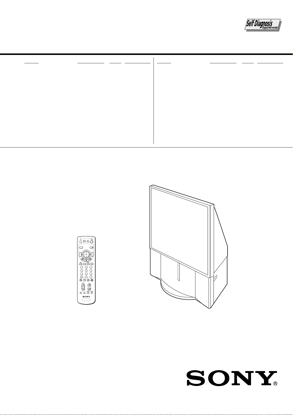
KP-FX43M31/M61/M91
KP-FX53M31/M61/M91
PROJECTION TV
Page 2
SPECIFICATIONS
KP-FX43M31/M61/M91
KP-FX53M31/M61/M91
RM-998
Projection system
Picture tube
Projection lenses
Screen size
Television system
Color system
Stereo/Bilingual
system
Channel coverage
B/G
I
D/K
M
(Antenna)
Audio output (Speaker)
Number of terminal
(Video)
(Audio)
(S Video)
(Component
Video)
(G/B/R/HD/
VD Video)
(Headphones)
Power requirements
Power consumption (W)
Dimensions (w/h/d, mm)
Mass (kg)
KP-FX53M31/M61/M91
3 picture tubes, 3 lenses, horizontal inline system
7 inch high-brightnes monochorome tubes (6.3 raster size), with optical coupling
and liquid cooling system
High performance, large-diameter highbrid lens F1.0
53 inches 43 inches
B/G, I, D/K, M
PAL, PAL 60, SECAM, NTSC4.43, NTSC3.58
NICAM Stereo/Bilingual B/G, I;
A2 Stereo/Bilingual (German) B/G
VHF : E2 to E12 / UHF : E21 to E69 / CATV : S01 to
S03, S1 to S41
UHF : B21 to B68 / CATV : S01 to S03, S1 to S41
VHF : C1 to C12, R1 to R12 / UHF : C13 to C57, R21
to R60 / CATV : S01 to S03, S1 to S41, Z1 to Z39
VHF : A2 to A13 / UHF : A14 to A79/
CATV : A-8 to A-2, A to W+4, W+6 to W+84
75-ohm external terminal
15W + 15W (10% distortion)
Input: 4 Output: 1 Phono jacks; 1 Vp-p, 75 ohms
Input: 4 Output: 1 Phono jacks; 500 mVrms
Input: 2 Y: 1 Vp-p, 75 ohms,
unbalanced, sync negative
C: 0.286 Vp-p, 75 ohms
Input: 2 Phono jacks
Y: 1 Vp-p, 75 ohms, sync negative
P
B/CB: 0.7 Vp-p, 75 ohms
P
R/CR: 0.7 Vp-p, 75 ohms
Audio: 500 mVrms
Input: 1 Phono jacks
G: 0.7 Vp-p, 75 ohms
B: 0.7 Vp-p, 75 ohms
R: 0.7 Vp-p, 75 ohms
HD: 0.7 Vp-p, 75 ohms
VD: 0.7 Vp-p, 75 ohms
Output: 1 Stereo minijack
110 - 240 V AC, 50/60Hz
260 W
1136 1438 666 926 1255 534
86 65.5
KP-FX43M31/M61/M91
Design and specifications are subject to change without notice.
CAUTION
SHORT CIRCUIT THE ANODE OF HTE PICTURE TUBE
AND THE ANODE CAP TO THE METAL CHASSIS, CRT
SHIELD, OR CARBON PAINTED ON THE CRT, AFTER
REMOVING THE ANODE.
SAFETY-RELATED COMPONENT WARNING!!
COMPONENTS IDENTIFIED BY SHADING AND MARK
! ON THE SCHEMATIC DIAGRAMS, EXPLODED
VIEWS AND IN THE PARTS LIST ARE CRITICAL TO
SAFE OPERATION. REPLACE THESE COMPONENTS
WITH SONY PARTS WHOSE PART NUMBERS APPEAR AS SHOWN IN THIS MANUAL OR IN SUPPLEMENTS PUBLISHED BY SONY.
– 2 –
Page 3

TABLE OF CONTENTS
1. SELF DIAGNOSIS FUNCTION
1-1. Diagnostic Test Indicators ................................. 5
1-2. Display of STANDBY/TIMER
Light Flash Count............................................... 6
1-3. Stopping the STANDBY/TIMER Flash ............ 6
1-4. Self-Diagnostic Screen Display ......................... 7
1-5. Handling of Self-Diagnostic
Screen Display.................................................... 7
1-6. Self-Diagnostic Circuit ...................................... 8
2. DISASSEMBLY
2-1. Rear Cover Removal ......................................... 9
2-2. Main Bracket Block Removal ........................... 9
2-3. Service Position ................................................. 9
2-4. Front Panel Removal ......................................... 10
2-5. H1, H2, and H3 Boards Removal ..................... 11
2-6. Beznet and Mirror Cover Removal ................... 11
2-7. Main Bracket Removal ...................................... 12
2-8. G Board Removal ............................................... 13
2-9. Connector Cover Removal ................................. 13
2-10. J Board Removal ................................................ 14
2-11. A1, E, B4 and v2 Boards Removal .................... 14
2-12. A, AD, and D Boards Removal ......................... 15
2-13. Picture Tube Removal ........................................ 15
2-14. High-Voltage and Cable Installation Removal.. 16
2-15. Mechaseal ........................................................... 16
3. SET-UP ADJUSTMENTS
3-1. Screen Voltage Adjustment
(Rough Alignment) ........................................... 17
3-2. Screen (G2) Adjustment .................................... 17
3-3. Focus Rough Adjustment .................................. 17
2-4. Deflection Yoke Tilt Adjustment ...................... 17
3-5. 2-Pole Magnet Adjustment ................................ 18
3-6. Center Magnet Adjustment ................................ 18
3-7. 4-Pole Magnet Adjustment ................................ 18
3-8. Defocus Adjustment ........................................... 18
3-9. Green, Red, and Blue Focus Adjustment
3-9-1. Green, Red, and Blue Lens Focus
Adjustment .................................................... 18
3-9-2. Green, Red, and Blue Electrical Focus
Adjustment .................................................... 18
3-10. Adjustment with Commander ............................ 19
3-10-1. How to Select Each Mode ............................. 19
- 3-10-2. How to Enter Service Mode .......................... 19
3-10-3. Method of Cancellation
from Service Mode ........................................ 20
3-10-4. How to Adjustments ...................................... 20
3-10-5. How to Write the Data ................................... 20
3-10-6. Memory Write Confirmation Method ........... 20
KP-FX43M31/M61/M91
KP-FX53M31/M61/M91
RM-998
Section Title PageSection Title Page
3-11. Service List ......................................................... 21
3-12. Registration Adjustment
3-12-1. Adjustment Flow ............................................ 49
3-12-2. Setup for Adjustment ..................................... 49
3-12-3. Method of Main Deflection Adjustment ....... 49
3-12-4. Operation Method
for Projector Engine (PJE) Mode .................. 50
3-12-5. Method of Projector Engine Adjustment
(Sub Deflection Adjustment)......................... 51
3-13. Auto Convergence Setting ................................. 54
3-14. Blue Offset Adjustment...................................... 54
3-15. White Balance Adjustment ................................ 54
3-16. Auto Convergence Error Code List ................... 55
4. SAFETY RELATED ADJUSTMENT
4-1. HV Regulation Adjustment ............................... 56
4-2. HV Hold-Down Adjustment ............................. 56
4-3. +B Max Voltage Confirmation ......................... 56
4-2. +B OVP Voltage Confirmation ........................ 56
5. ELECTRICAL ADJUSTMENTS
5-1. Picture Quality Adjustment
5-1-1. Preparation ..................................................... 57
5-1-2. NTSC Video Input ......................................... 58
5-1-3. NTSC RF Input .............................................. 57
5-1-4. PAL Video Input ............................................ 59
5-1-5. PAL RF Input ................................................. 59
5-2. Color Offset ........................................................ 60
6. DIAGRAMS
6-1. Block Diagrams .................................................. 61
6-2. Frame Schematic Diagram................................. 77
6-3. Circuit Boards Location ..................................... 79
6-4. Schematic Diagrams and Printed Wiring Boards 80
(1) A Board ......................................................... 81
(2) A1 Board ....................................................... 91
(3) AD Board ...................................................... 95
(4) B4 Board ....................................................... 107
(5) CR,CG and CB Boards ................................. 123
(6) D Board ......................................................... 129
(7) E Board.......................................................... 139
(8) G Board ......................................................... 143
(9) H1,H2 and H3 Boards................................... 147
(10) J Board .......................................................... 151
(11) SR , V2 and VM Boards ............................... 167
6-5. Semiconductors .................................................. 171
– 3 –
Page 4

Section Title Page
7. EXPLODED VIEWS
7-1. Front Panel Block ............................................. 174
7-2. Cabinet Block (KP-FX53) ............................... 175
7-3. Cabinet Block (KP-FX43) ................................ 176
7-4. Bezenet and Mirror Cover Block (KP-FX53) .. 177
7-5. Bezenet and Mirror Cover Block (KP-FX43) ... 178
7-6. Main Braket and Picture Tube Block ................ 179
8. ELECTRICAL PARTS LIST ............................ 180
KP-FX43M31/M61/M91
KP-FX53M31/M61/M91
RM-998
– 4 –
Page 5

KP-FX43M31/M61/M91
KP-FX53M31/M61/M91
SECTION 1
SELF DIAGNOSIS FUNCTION
The unit in this manual contain a self-diagnostic function. If any error occurs, the STANDBY/TIMER lamp will automatically
begin to flash.
The number of times the lamp flashes translates to a probable source of the problem. A definition of the STANDBY/TIMER
lamp flash indicators is listed in the instruction manual for the user's knowledge and reference. If an error symptom cannot be
reproduced, the remote commander can be used to review the failure occurrence data stored in memory to reveal past problems
and how often these problems occur.
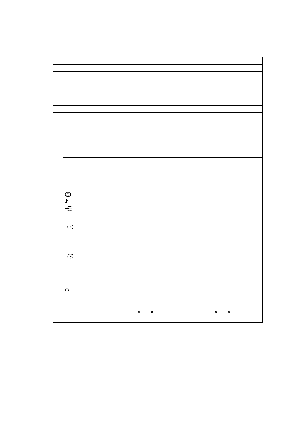
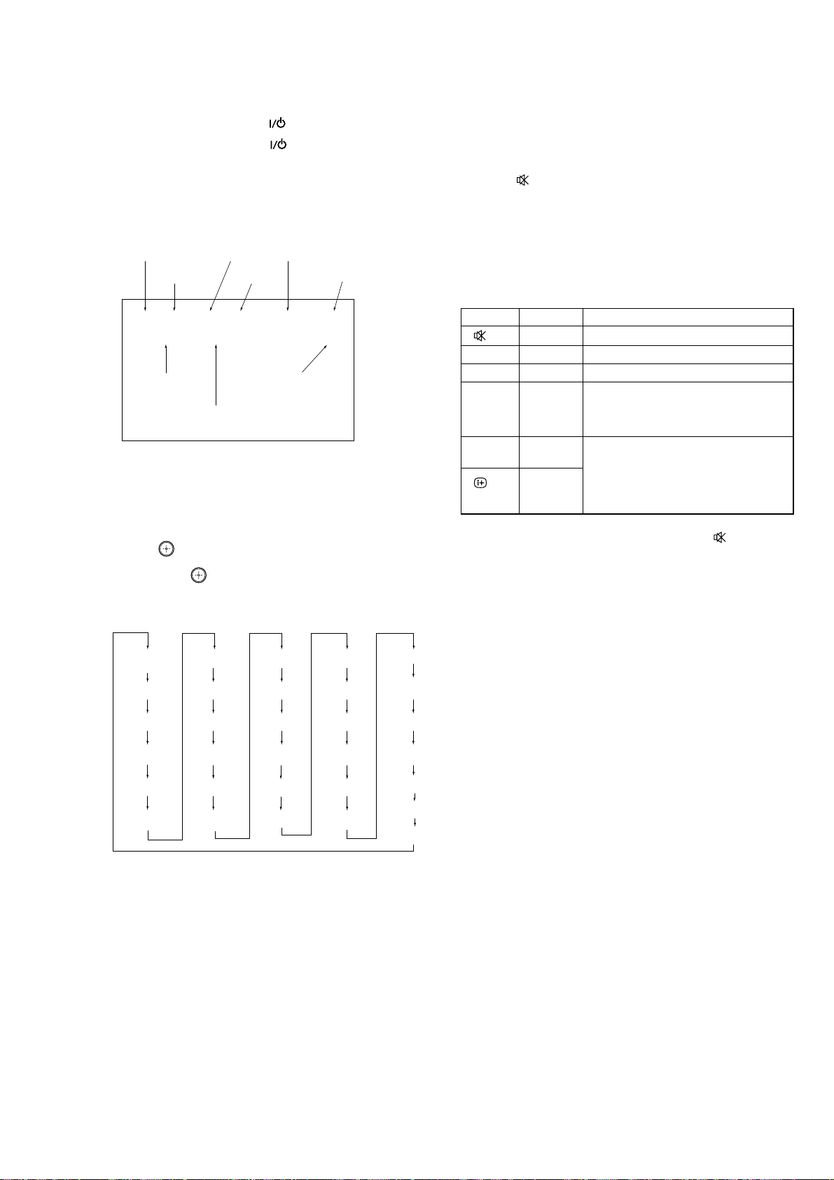
1-1. DIAGNOSTIC TEST INDICATORS
When any error occurs, the STANDBY/TIMER lamp will flash a set number of times to indicate the possible cause of the
problem. If there is more than one error, the lamp will identify the first of the problem areas.
Result for all of the following diagnostic items are displayed on screen. No error has occurred if the screen displays a “0”.
RM-998
Diagnostic
Item
Description
•Power does not
turn on
•+B overcurrent
(OCP)
•+B overvoltage
(OVP)
•Vertical deflection
failure
•White balance
failure
(no PICTURE)
•
Horizontal deflection
failure or +5v down
or High Voltage
failure
No. of times
STANDBY/TIMER
lamp flashes
Does not light
2 times
3 times
4 times
5 times
6 times
Self-diagnostic
display/
Diagnostic result
002:000 or
002:001 ~ 255
003:000 or
003:001 ~ 255
004:000 or
004:001 ~ 255
005:000 or
005:001 ~ 255
006:000 or
006:001 ~ 255
Probable Cause Location
•Power cord is not plugged in.
•Fuse (F6701) is burned out.
(G board)
•H. OUT Q8024 is shorted.
•H. LIN Q8027 is shorted.
(D board)
•HV OUT Q8043 is shorted.
•PH6001 faulty.
•+19V is not supplied.
(G board)
•V. OUT IC8003 faulty.
(D board)
•G2 is improperly adjusted.
(Note 1)
•CRT problem.
•Video OUT IC9101 (CR
board), IC9201 (CG board),
IC9001 (CB board) are faulty.
•IC8306 (J board) and IC4300
(E board) are faulty.
•No connection E board to CR
board.
•IC6502 (G board) faulty.
•HV Circuit failure.
Detected Symptoms
•Power does not come on.
•No power is supplied to the PJ.
•AC power supply is faulty.
•Power does not come on.
•Load on power line is shorted.
•+135V is too high.
•Vertical deflection pulse is
stopped.
•Vertical size is too small.
•Vertical deflection stopped.
•No raster is generated.
•CRT cathode current detection
reference pulse output is small.
•Abnormal High voltage.
•Abnormal H.drive.
•+5v down.
•Audio Protection
•Micro reset
Note 1 : Refer to screen (G2) adjustment in section 3-2 of this manual.
7 times
007:000 or
007:001 ~ 255
101:000 or
101:001 ~ 255
•Power supply fails.
•IC1203,1204 (A board) faulty.
•Discharge CRT
(CR, CG, CB boards)
•Static discharge
•External noise
– 5 –
•There is picture but speaker does
not release sound.
•Power is shut down shortly, after
this return back to normal.
•Detect Micro latch up.
Page 6
1-2. DISPLAY OF STANDBY/TIMER LIGHT FLASH COUNT
2 times
3 times
Lamp ON
0.3 sec.
Lamp OFF
0.3 sec.
4 times
5 times
Lamp OFF
3 sec.
KP-FX43M31/M61/M91
KP-FX53M31/M61/M91
RM-998
6 times
7 times
Diagnostic Item Flash Count *
+B overcurrent 2 times
+B overvoltage 3 times
V deflection stop 4 times
White balance failure 5 times
High voltage protector 6 times
Audio Protection 7 times
* One flash count is not used for self-diagnostic.
STANDBY/TIMER
lamp
1-3. STOPPING THE STANDBY/TIMER FLASH
Turn off the power switch on the TV main unit or unplug the power cord from the outlet to stop the STANDBY/TIMER lamp from
flashing.
– 6 –
Page 7
KP-FX43M31/M61/M91
KP-FX53M31/M61/M91
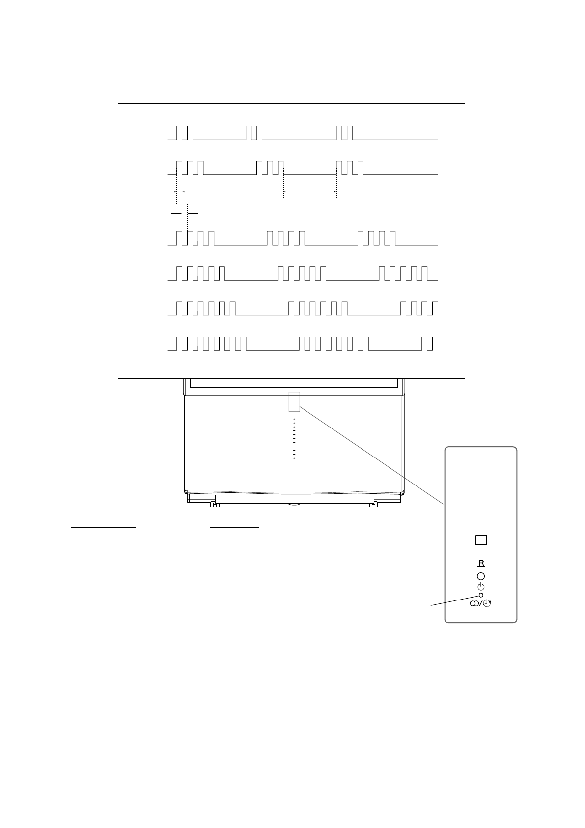
1-4. SELF-DIAGNOSTIC SCREEN DISPLAY
For errors with symptoms such as “power sometimes shuts off” or “screen sometimes goes out” that cannot be confirmed, it is
possible to bring up past occurrences of failure for confirmation on the screen:
[To Bring Up Screen Test]
In standby mode, press buttons on the remote commander sequentially in rapid succession as shown below:
Self-Diagnosis screen display
1-5. HANDLING OF SELF-DIAGNOSTIC SCREEN DISPLAY
5
RM-998
(
DISPLAY
Since the diagnostic results displayed on the screen are not automatically cleared, always check the self-diagnostic screen
SELF DIAGNOSTIC
(DIGIT 5) (VOLUME –) (POWER)ON SCREEN
)
002:000
*
* : Note that this differs from entering the service mode (volume +)
Numeral “0” means that no fault has been detected.
003:000
004:000
005:001
006:002
Numeral “1” means a fault has been detected.
Numeral “2” means two faults have been detected.
007:000
101:000
during repairs. When you have completed the repairs, clear the result display to “0”.
Unless the result display is cleared to “0”, the self-diagnostic function will not be able to detect subsequent faults after completion of the repairs.
[Clearing the result display]
To clear the result display to “0”, press button on the remote commander sequentially as shown below when the diagnostic
screen is being displayed.
Press “8” button
(It will indicate “CLEAR” on the screen.)
,
(The “CLEAR” display change to red color.)
Press “-” button
[Quitting Self-diagnostic screen]
To quit the entire self-diagnostic screen, turn off the power switch on the remote commander or the main unit.
– 7 –
Page 8
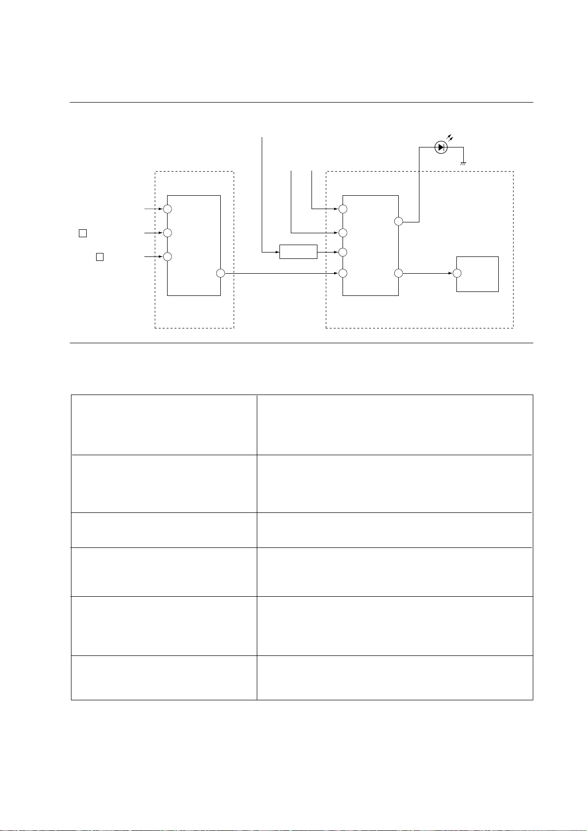
1-6. SELF-DIAGNOSTIC CIRCUIT
IC4300
Y/C JUNGLE
From IC1203,1204
(A board)
From G board
OCP
OVP
KP-FX43M31/M61/M91
KP-FX53M31/M61/M91
RM-998
To H1 board
IC001
SYSTEM
24 IKINFrom CRT (IK)
H
V
(D board)
(D board)
57 XRAYFrom IC8005,8006
56 V PROTFrom Q8001
SDA 52 13 SDA0 SDA1 SDA15 5
Q1209-1211
5 OCP
8 OVP
100
SPPROT
LED1 22
IC003
MEMORY
CXA2170Q CXP961048-006Q
A boardE board
+B overcurrent (OCP) Occurs when an overcurrent on the +B (135 V) line is detected by
Q6504.
Then the voltage to pin 5 of IC001 goes UP. The unit will automatically
turn off.
+B overvoltage (OVP) Occurs when an overvoltage on the +B (135 V) line is detected by
IC6502.
Then the voltage to pin 8 of IC001 goes UP. The unit will automatically
turn off.
Vertical deflection failure Occurs when an absence of the vertical deflection pulse is detected by
Q8001 and D8001. Shut down the power supply.
White balance failure If the RGB levels do not balance or become low level within 5 seconds.
This error will be detected by IC4300.
TV will stay on, but there will be no picture.
High voltage or Horizontal Deflection Protect Occurs when an overvoltage of horizontal pulse is detected by D8038
and IC8006.
If the voltage of pin 1 of IC8006 goes to High, the voltage to pin 57 of
IC4300go to UP. The unit will automatically turn off.
Audio Protector If the Audio out lines become DC.This error will be detected by Q1211,
Q1209 and Q1210.
The unit will automatically turn off.
– 8 –
Page 9
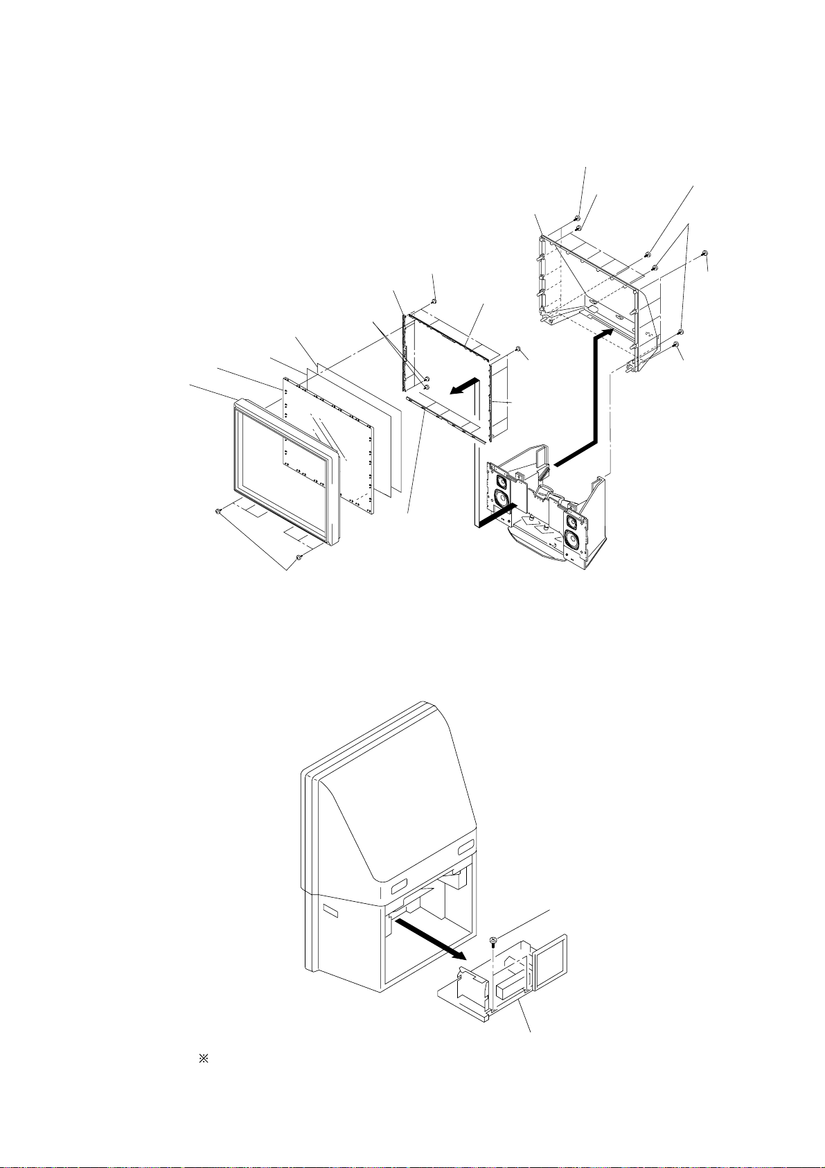
SECTION 2
DISASSEMBLY
2-1. REAR COVER REMOVAL
(1) KP-FX43 (2) KP-FX53
KP-FX43M31/M61/M91
KP-FX53M31/M61/M91
RM-998
2 Rear board
1 Eleven screws
(Hexagon head)
2-2. MAIN BRACKET REMOVAL
2 Rear board
1 Eleven screws
(Hexagon head)
2-3. SERVICE POSITION
1 Optical shield
2 Two screws
(tapping screw
hexagon head)
3 Main bracket section
2 Eight screws
(BVTP 3X12)
1 Main bracket section
2 COVERS
Cut them off with a plier or the like from
chassis assembly in case of checking
printed circuit boards.
After checking, turn over the covers and
secure them with screws.
(screws 7-685-648-79 -BVTP 3X12)
– 9 –
Page 10
2-4. FRONT PANEL REMOVAL
y
(1) KP-FX43
KP-FX43M31/M61/M91
KP-FX53M31/M61/M91
RM-998
2 Three screws
(tapping screw
hexagon head)
4 Side panel (43L) assy
1 Three screws
(BVTP 4x16)
6 Front panel (43) assy
3 T wo screws
(tapping screw
hexagon head)
3 T wo screws
(tapping screw
hexagon head)
1 Three screws
(BVTP 4X16)
2 Three screws
(tapping screw
hexagon head)
5 Side panel (43R) assy
(2) KP-FX53
4 Side pane (53L) assy
1 Three screws
(BVTP 4x16)
6 Front panel (43) ass
2 Three screws
(tapping screw
hexagon head)
3 T wo screws
(tapping screw
hexagon head)
3 T wo screws
(tapping screw
hexagon head)
1 three screws
(BVTP 4x16)
2 Three screws
(tapping screw
hexagon head)
5 Side pane (53R) assy
– 10 –
Page 11
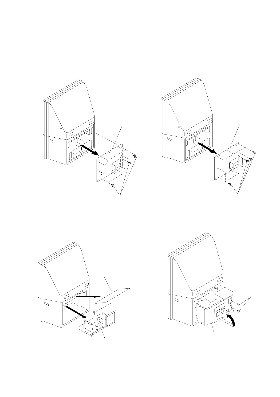
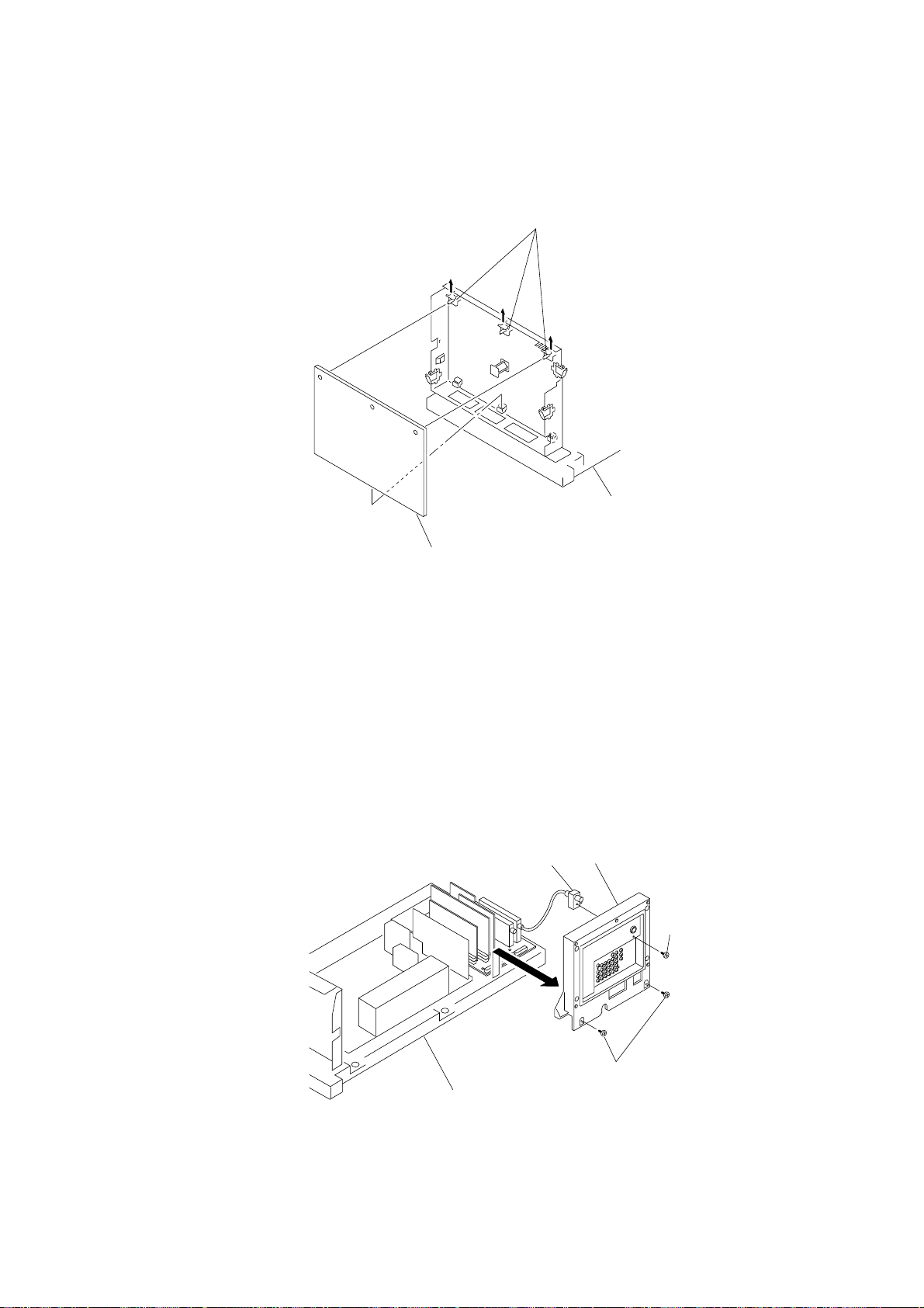
2-5. H1, H2 AND H3 BOARDS REMOVAL
KP-FX43M31/M61/M91
KP-FX53M31/M61/M91
RM-998
8 Four screws
(BVTP 3x12)
9 H3 board
3 H1 board
6 Two screws
(BVTP 3x12)
2 H1 bracket
1 Two screws
(BVTP 3x12)
4 Six screws
(BVTP 3x12)
5 H2 board
6 Three screws
(BVTP 3x12)
7 Control button
Front panel assy
2-6. BEZNET AND MIRROR COVER REMOVAL
(1) KP-FX43
!¢ Holder Bracket(43L)
5 Six screws (BVTP 4X16)
7 Screen holder (SIDE)
5 Twelve screws (BVTP 4X16)
!£ Diffusion plate (F)
!™ Diffusion plate (L)
0 Beznet assy
!¡ Contrast screen
9 Screen
holder (LOW)
4 Mirror cover
6 Screen
holder (TOP)
5 Four screws
(BVTP 4X16)
8 Screen
holder (SIDE)
2 Four screws
(BVTP 4X16)
2 Six screws
(BVTP 4X16)
1 T wo screws
(Hexagon head)
2 Four screws
(BVTP 4X16)
1 Four screws
(Hexagon head)
!¢ Holder
Bracket(43R)
3 Six screws
(Hexagon head)
– 11 –
Page 12
2-6. BEZNET AND MIRROR COVER REMOVAL
(
)
(2) KP-FX53
3 Mirror cover
KP-FX43M31/M61/M91
KP-FX53M31/M61/M91
2 Six screws
(BVTP 4X16 )
2 Six screws
(BVTP 4X16)
1 T wo screws
(Hexagon head)
RM-998
2 T wo screws
(Hexagon head)
!™ Diffusion plate (L)
0 Beznet assy
!¡ Contrast screen
7 Screen holder (SIDE)
5 Twelve screws (BVTP 4X16)
!£ Diffusion plate (F)
3 Six screws
5 Six screws (BVTP 4X16)
9 Screen
holder (LOW)
Hexagon head
6 Screen
holder (TOP)
5 Four screws
(BVTP 4X16)
8 Screen
holder (SIDE)
2 Six screws
(BVTP 4X16)
1Four screws
(Hexagon head)
2-7 MAIN BRACKET REMOVAL
Pay particular attention to the wires
of each printed circuit boards when
puling out the mainbracket.
1 T w o screws
(Tapping screw
hexagon head)
2 Main bracket section
– 12 –
Page 13
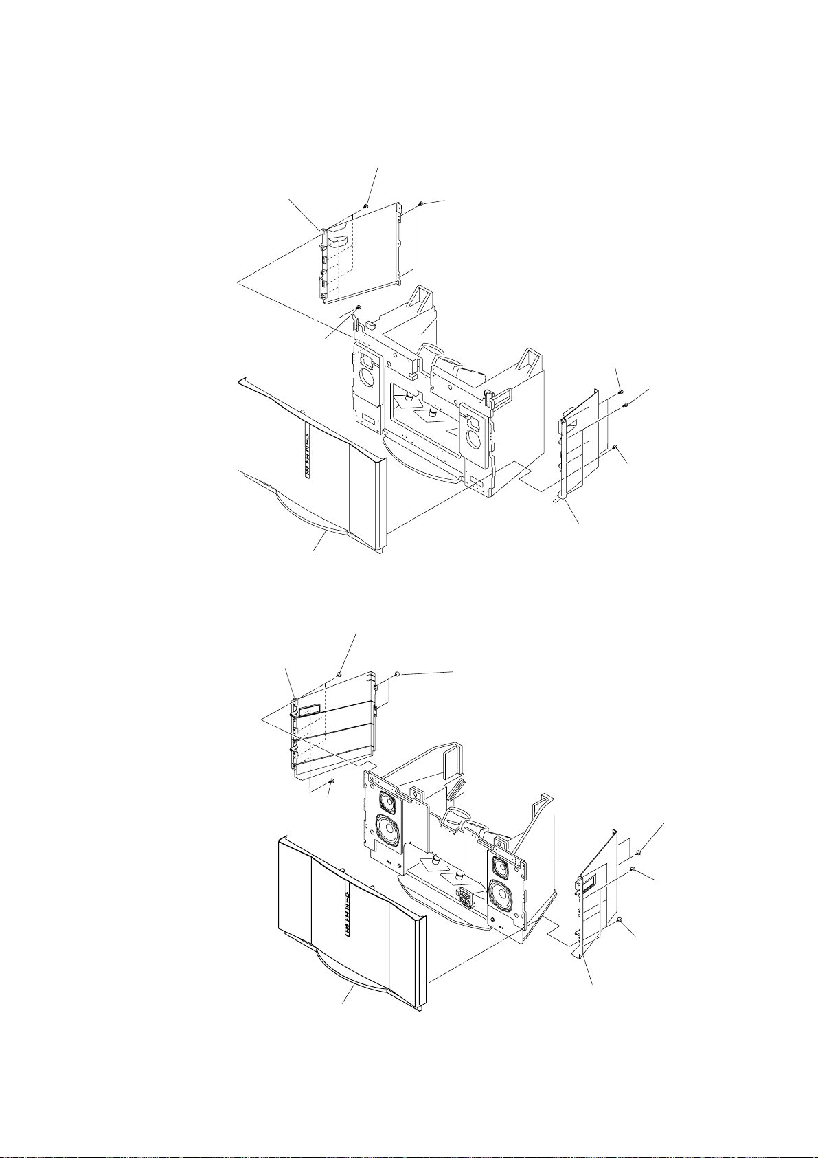
2-8. G BOARD REMOVAL
KP-FX43M31/M61/M91
KP-FX53M31/M61/M91
RM-998
1 Three holder PWB
2-9. CONNECTOR COVER REMOVAL
2 G board
RF Connector
Main bracket section
3 Connector cover section
2 Screw
(PSW 2.6X6)
Main bracket section
– 13 –
1 T o w screws
(BVTP 4X16)
Page 14
2-10. J BOARD REMOVAL
KP-FX43M31/M61/M91
KP-FX53M31/M61/M91
RM-998
5 Connector cover
4 J board
2 J board cover
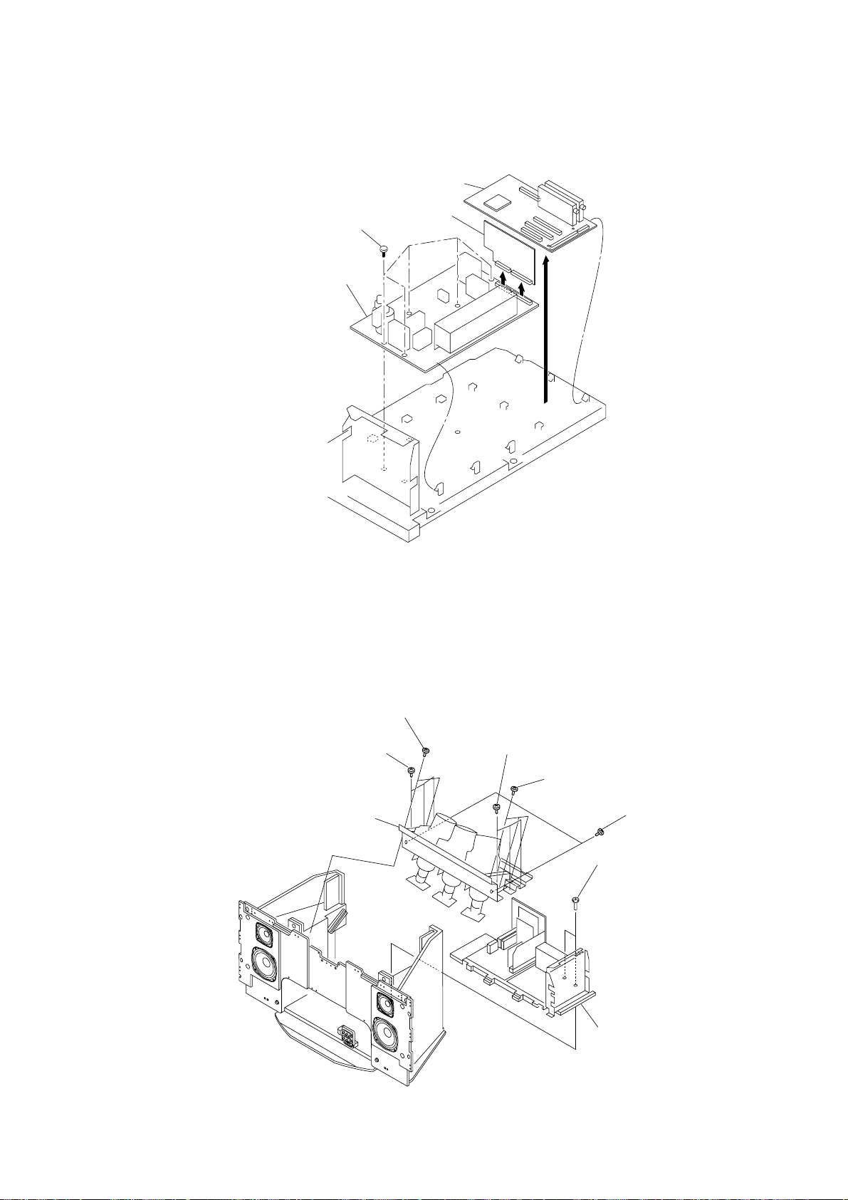
2-11. A1, E, B4, AND V2 BOARDS REMOVAL
3 Four screws
(BVTP 3X12)
2 E board
1 A1 board
3 B4 board
4 V2 board
– 14 –
Page 15
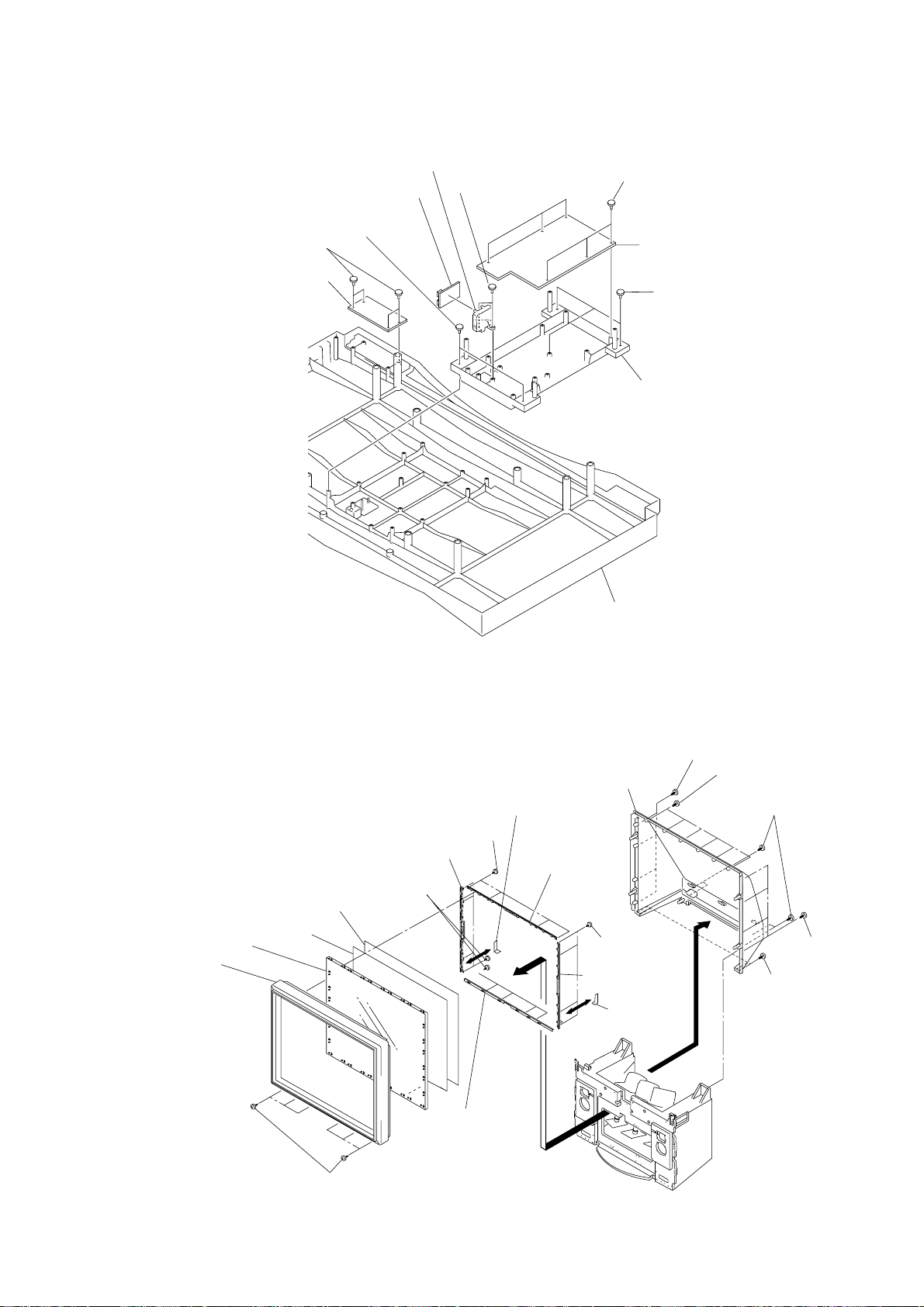
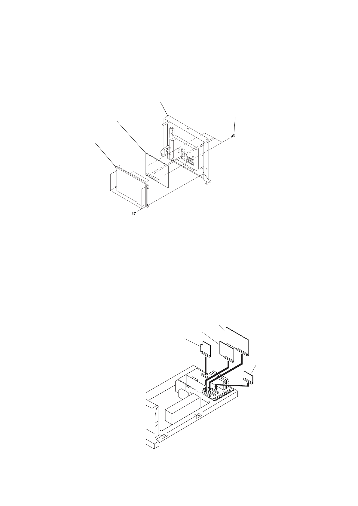
2-12. A, AD AND D BOARDS REMOVAL
KP-FX43M31/M61/M91
KP-FX53M31/M61/M91
RM-998
1 A board
3 Five screws
(BVTP 3X12)
4 D board
2 AD board
2-13. PICTURE TUBE REMOVAL
2 Three screws
(Hexagon head)
(4X20)
4 Picture tube block assy
1 Two screws
(BVTP 4X16)
2 Three screws
(Hexagon head)
(4X20)
1 Three screws
(BVTP 4X16)
3 Three screws
(BVTP 4X20)
5 Two screws
(Hexagon head)
(4X20)
6 Main bracket section
– 15 –
Page 16
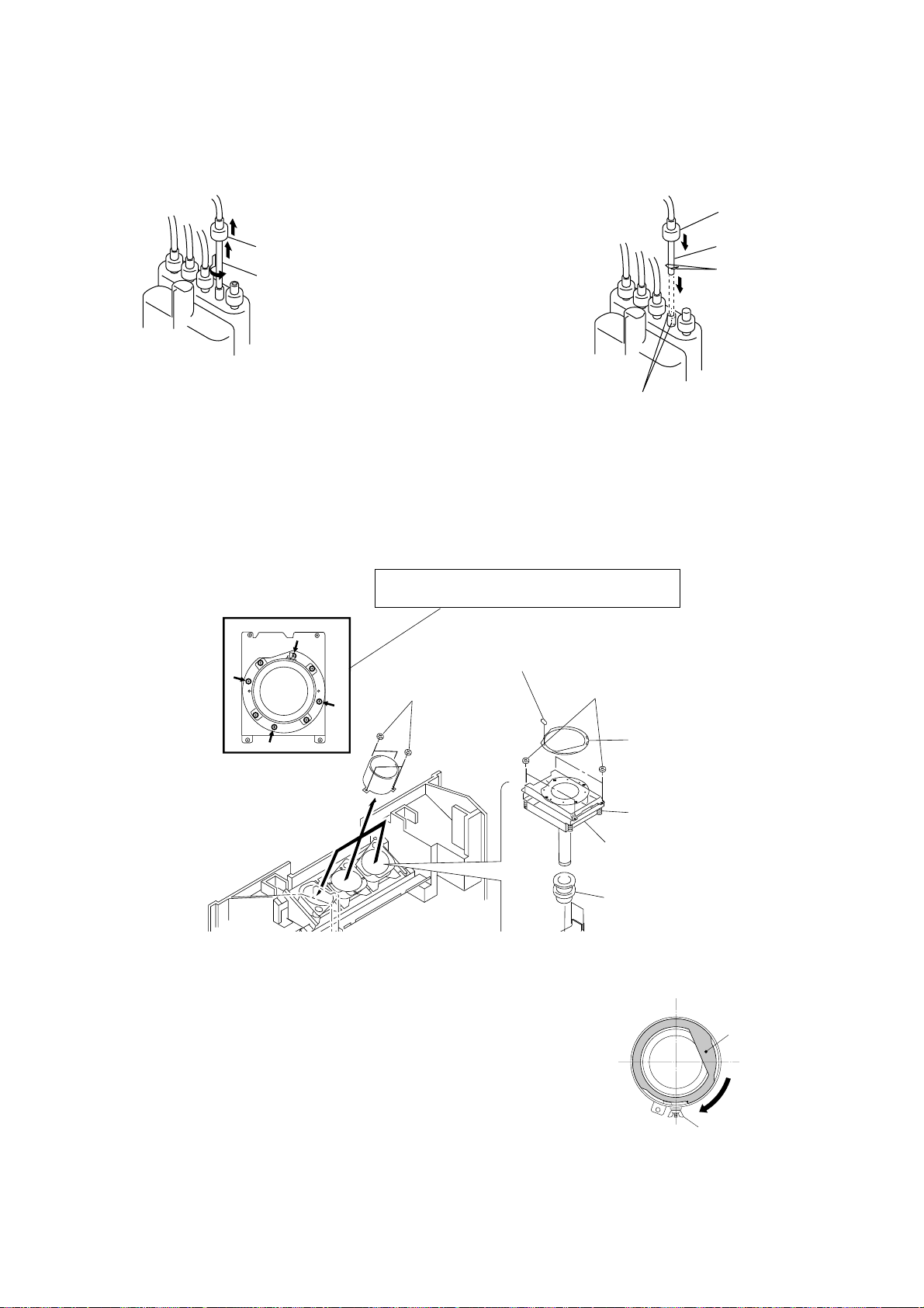
2-14 HIGH-VOLTAGE CABLE
Shading
Fly nut
INSTALLATION AND REMOVAL
KP-FX43M31/M61/M91
KP-FX53M31/M61/M91
RM-998
(1) Remover
2-15. MECHASEAL
1 Rubber cap
2 HV cable turn 90°
(2) Installation
2 Rubber cap
1 HV cable
Hook
Gutter
Removing the arrow-marked screw is strictly inhibited.
If removed, it may cause liquid spill.
9 Cushion (Geen, Red only)
1 Four screws
(BVTP 4X16)
: 1.When installing the Machaseal assy (RED, and GREEN),
*
be sure to reuse the Plate shading.
2.Check alignment to make sure the Plate shadings are the right
positions as following Fig 2-5.
5 Four screws
(BVTP 4X16)
8 *Plate shading (Green, Red only)
7 Extension spring
6 Mechaseal assy (R)
4 Deflection yoke
Fig 2-5
– 16 –
Page 17
SECTION 3
SET-UP ADJUSTMENTS
KP-FX43M31/M61/M91
KP-FX53M31/M61/M91
RM-998
3-1. SCREEN VOLTAGE ADJUSTMENT
(ROUGH ALIGNMENT)
1. Receive the Monoscope signal.
2. Set 50% BRIGHTNESS and minimum PICTURE.
3. Turn the red VR on the focus pack all the way to the left and
then gradually turn it to the right until the point where you
can see the retrace line.
4. Next gradually turn it to the left to the position where the
retrace line disappears.
Focus Pack
FOCUS
B
BRG
RG
SCREEN
Fig. 3-1
3-2. SCREEN (G2) ADJUSTMENT
(FINE ADJUSTMENT)
1. Turn on the power of the set.
2. Select VIDEO1 mode without signal.
3. Supply DC 175 ± 0.5 V from external power supply to KR,
KG or KB of CR board, CG board and CB board.(Fig.3-2)
4. Adjust red, green and blue screen voltage to until retrace
line disappears with screen VR on the focus pack.
5. Confirm if retrance can be seen.
5. Rotate the green lens and align to obtain the best lens focus
at the center area.
6. Rotate the green focus VR on the focus pack and align to
obtain the best electrical focus in the center area.
7. Perform the same alignment for red and blue lenses and electric focus.
8. Fix lens screw.
Scanning line visible.
A
Minimize both A and B.
Lens
Fig. 3-4
B
Fig. 3-5
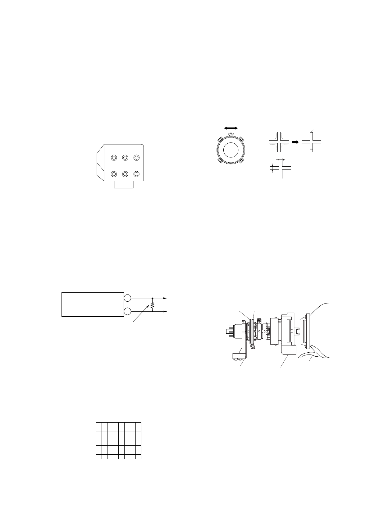
3-4. DEFLECTION YOKE TILT ADJUSTMENT
1. Receive the Monoscope signal.
2. Place the caps on the red and blue lens so that only the green
color.
3. Loosen the deflection yoke setscrew and align the tilt of the
Deflection yoke so that the bars at the center of the
monoscope pattern are horizontal.
4. After aligning the deflection yoke, fasten it securely to the
funnel-shaped portion of the CRT.
5. The tilt of the deflection yoke for red and blue is aligned the
same as was done for green.
Power
Supply
+
–
Dummy Resister
3k ohm 20W
Fig. 3-2
3-3. FOCUS ROUGH ADJUSTMENT
1. Loose the lens screw.
2. Set in the service mode.
3. Place the caps on the red and blue lens so that only the green
color is shown.
4. Press “1” or “4” button on the commander and select
“PJE”, press “6” three times on the Commander to display
the test signal (crosshatch) on the screen.
Test signal
Fig. 3-3
4 Pole Magnet
2 Pole Magnet
Holder
Make sure deflection yoke is
touching CRT closely.
Deflection Yoke
Fig. 3-6
Anode cap
– 17 –
Page 18
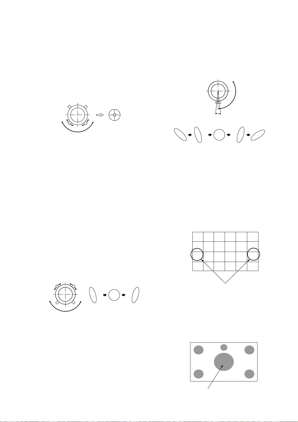
3-5. 2-POLE MAGNET ADJUSTMENT
1. Receive the Dot signal.
2. Place the caps on the red and blue lens so that only the green
color is shown.
3. Turn the green focus VR on the focus pack to the left and set
to under focus to enlarge the spot.
4. Adjust the 2-Pole Magnet so that the bright spot should be
centerd.
(center of the dot doesn't move)
5. Align the green focus VR and set for just (precise) focus.
KP-FX43M31/M61/M91
KP-FX53M31/M61/M91
RM-998
3-8. DEFOCUS ADJUSTMENT (BLUE)
1. Receive the Dot signal.
2. Cover the both red and green picture lenses with the lens
caps to show only the color.
3. Turn the blue focus VR on the focus pack to the right to
make the round dot elipical.
4. Set 4 pole magnet tab angle 12°.
5. Rotate 4 pole magnet keeping Tab angle 90° make the spot
shape vertical ellipse.
Use the center dot
Fig. 3-8
3-6. CENTERRING MAGNET ADJUSTMENT
1. Receive the SPCB signal.
2. Cover the both red and blue picture lenses with the lens caps
to show only the color.
3. Adjust the green centering magnet to put the center of the
SPCB signal to the center of the screen.
4. Adjust red centering magnet in the same way.
5. Adjust blue centering magnet in the same way.
3-7. 4-POLE MAGNET ADJUSTMENT
1. Receive the Dot signal.
2. Place the caps on the red and blue lens so that only the green
color is shown.
3. Turn the green focus VR on the focus pack to the right and
set to over focus to enlarge the spot.
4. Now align the 4-Pole Magnet so that the enlarged spot becomes a perfect circle.
5. Perform the same alignment for red.
Rotate
12° Fix
OK
Fig. 3-10
3-9. GREEN, RED AND BLUE FOCUS
ADJUSTMENT
3-9-1. Green, Red and Blue Lens Focus Adjustment
1. Receive the cross hatch signal.
2. Place the caps on the red and blue lens so that only the green
color is shown.
3. Rotate the green lens and adjust to obtain the best lens focus
at the center area.
4. Fix lens screw.
5. Repeat above process for red and blue.
6. Rotate the blue lens and adjust to obtain the best lens focus at
the both side area.
7. Fix blue lens screw.
Use the center dot
Fig. 3-9
OKNG NG
Adjust Point of Blue
Fig. 3-11
3-9-2. Green and Red Dot/Hatch Electrical Focus
Adjustment
1. Receive the signal.
2. Place the caps on the red and blue lens so that only the green
color is shown.
3. Rotate the green focus VR on the focus pack and adjust to
obtain the best electrical focus in the adjust point.
4. Repeat above process for red and blue.
Adjust Point of Green and Red
Fig. 3-12
– 18 –
Page 19
KP-FX43M31/M61/M91
Enter the
“Service mode”
5
(DIGIT 5) (VOLUME +)ON SCREEN
DISPLAY
(
)
TV
STANDBY
(
)
KP-FX53M31/M61/M91
RM-998
3-10. ADJUSTMENTS WITH COMMANDER
Service adjustment to this model can performed with the supplied
remote commander RM-998
Copy PAL data
to NTSC
Write data to NVM
blue
Adjustment item
up
Adjustment item
down
User control goes
to the standard state
Read data from
NVM
Change
the PICTUER MODE
VIDEO
DRC-MF
P
R
N
I
O
W
G
T
INDEX
PROG
+
–
T
G
W
O
I
R
N
P
HD/DVD
123
456
7809
PROG
A/B
MENU
JUMP
Up : Category up
Down : Category down
Push : Enter
Copy data to all
mode
Data up
Data down
Initialize data
(Not stored)
3-10-1. How to Select Each Mode
50 Hz 60 Hz WIDE 60 Hz WIDE 50 Hz
(PAL) (NTSC) (NTSC) (PAL)
DRC1250 aa a a
DRC100 aa a a
TWIN aa
INDEX aa
1. Selection of Mode Between 50 Hz and 60 Hz
50 Hz : Enter the PAL signal.
60 Hz : Enter the NTSC signal.
WIDE 60 Hz : Enter the NTSC signal MENU WIDE ON.
WIDE 50 Hz : Enter the PAL signal MENU WIDE ON.
2. Selection of DRC Mode
1) Press “DRC-MF (blue)” button on the commander, repeatedly until displays the mode that you want to select on the
screen.
→ DRC1250 → DRC100 → PROGRESSIV
Note : The DRC-MF mode is not selectable when using the
“PROGRAM INDEX” or “TWIN” mode is turned “ON”.
XX
XX
OPTION RESET
TV
3. Selection of WIDE mode
1) Press “MENU” button on the commander and move “
” up
or down to enter the “FEATURE” b “WIDE MODE”.
2) Move “
” up or down to select “ON” or “OFF”, and push
“ (ENTER)” button.
3) Press “MENU” button to return to normal screen.
4. Selection of TWIN mode
1) Press “
2) Press “
(TWIN)” button on the commander.
(TWIN)” button again to return to normal screen.
5. Selection of INDEX mode
1) Press “PROGR INDEX” button on the commander.
2) Press “PROGR INDEX” button again to return to normal
screen.
3-10-2. How to Enter Service Mode
1. Turn on the main power switch to place this set in standby
mode. (LED will light in red.)
2. Press the buttons on the commander as follows, and enter service mode.
– 19 –
Page 20
3-10-3. Method of Cancellation from Service
Mode
1. Set the standby mode (Press “ (TV STANDBY)” button on
the commander), then press “
(TV
STANDBY)” button again, hereupon it becomes TV mode.
3-10-4. How to Adjustments
1. Set in the service mode, the following screen will appear.
Category Name Item Name Mode
Item No.
GE1 00 VPS 1C SERVICE 50
0 006Q 2.9M 00 00 01B7
Suffix No.
Software
Version
Data
Total Power On time
(Hours)
2. Press “1” or “4” button on the commander to select the adjustment item.
3. Press “3” or “6” button on the commander to change the
adjustment data.
4. Move “
” up or down to select the adjustment category.
When move “ ” up (category up), service mode changes in
the order as shown below.
GE1
GE2
DCN
LDG
AP
MSP
50 : PAL, SECAM
60 : NTSC
MD4
MD5
2CM
TXT
KP-FX43M31/M61/M91
KP-FX53M31/M61/M91
RM-998
3-10-5. How to Write the Data
1. Set in the service mode.
2. Press “1” or “4” button on the commander, select the adjustment item, and press “3” or “6” button to change the
data.
3. Press “
cate “WRITE” on the screen.
4. Press “-” button on the commander to write into memory.
(The “WRITE” display will be changed to red color while
executing, and back to “SERVICE”.)
Commander Function (Except PJE mode)
Button Mode Description
+ - WRITE Writes data to NVM.
7 + - READ Reads data from NVM.
8 + - NORMAL All user control goes to the standard.
5 + - INITIAL Service data initialization.
2 + - COPY Do not operate with a remote
+ - WRT5060 (The data vary with among mode.)
Note : Before changing to other modes, press “ (MUTE)” +
(MUTE)” button on the commander and it will indi-
Not stored.
(Be sure not to use usually)
commander.
“-” buttons on the commander to write the data.
(Omission of this operation causes the data to be returned
to the data before adjustment.)
: Confirm the adjustment mode before writing data for data
values because to vary in each adjustment mode.
: The adjustment item that there are no relations in the ad-
justment is not to change data values because all items are
written in each adjustment mode.
GE3
GE4
WHB
SAJ
* : When it moves from PJE to other categrys,
repeat 1 or 4 button and press it.
JGL
YCT
SYC
SYN
LTI
MD1
MD2
MD3
MD6
MD7
3NR
3CM
WID
PJE*
OSD
OPM
OPB
3-10-6. Memory Write Confirmation Method
1. After adjustment, turn off the AC main power switch off.
2. Turn the power switch ON and set in service mode.
3. Call the adjustment items again to confirm adjustments were
made.
– 20 –
Page 21
Note
• Common : The data value of each mode. Other are set up by each mode.
• : Shaded items are fixed data.
• : Though data value is indicated on the screen, it is not used.
• Standard data listed on the Adjustment Item Table are reference valies, therefore it may be different for each model and e
• Note for Different Data :
Those are the standard data values written on the microprocessor. Therefore , the data values of the modes and stored respec
In case of a device replacement, adjustment by rewriting the data value is necessary for some items.
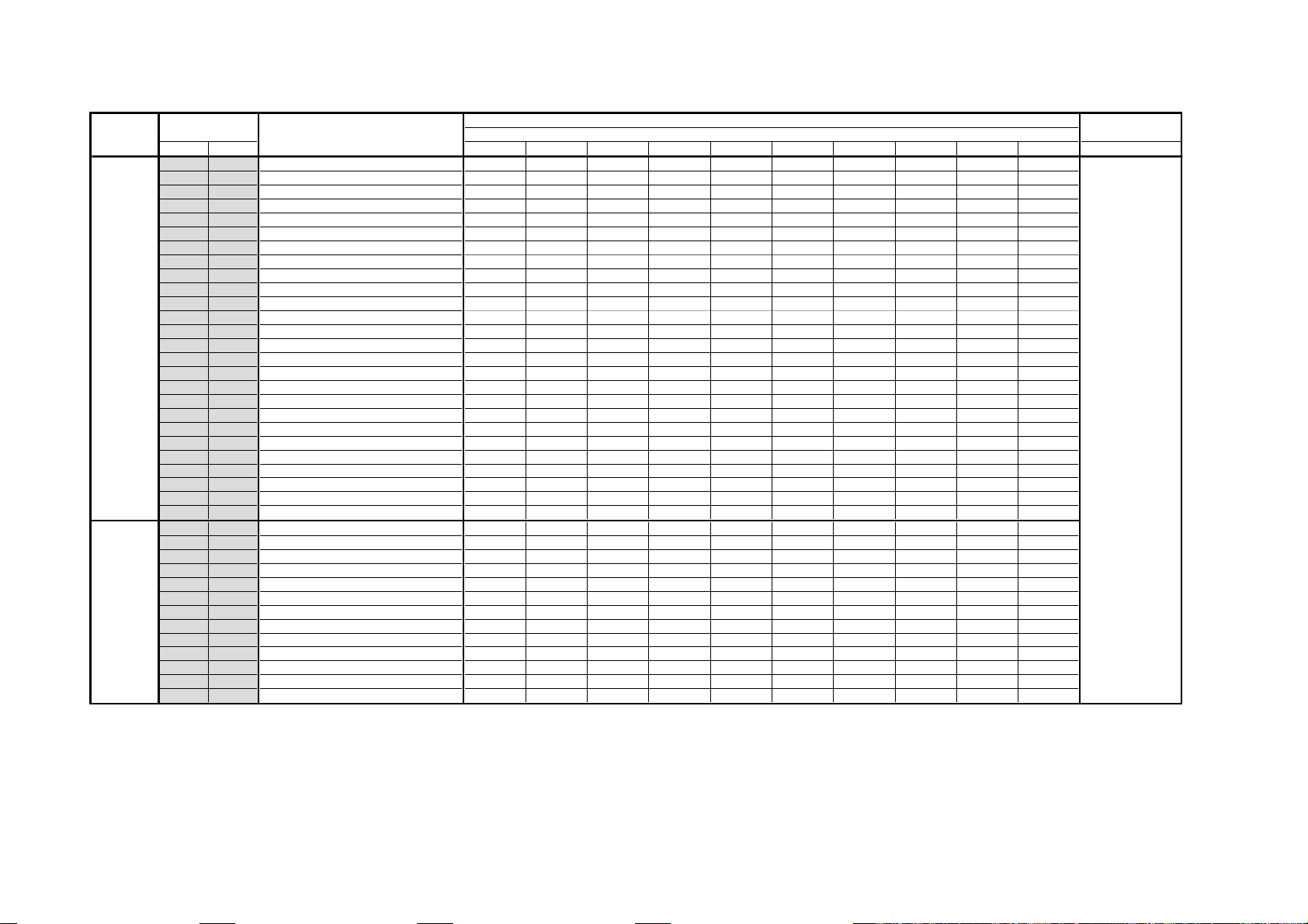
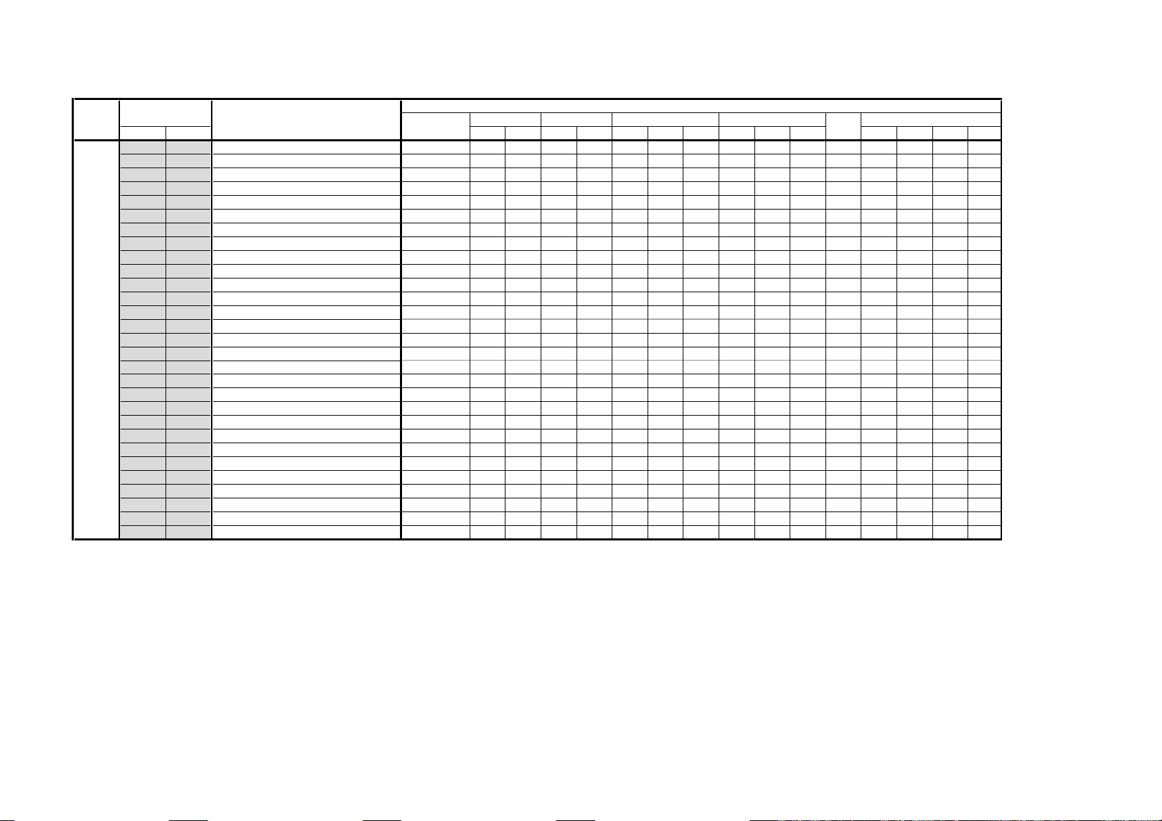
3-11. SERVICE LIST
ach mode.
tively in the memory.
– 21 –
Category
Item
No. Name
GE1 00 VPS
GE2 00 HCT
01 VSZ
02 VZO
03 VLN
04 VSC
05 VCN
06 VPN
07 MVP
08 HTZ
09 MHZ
0A ZOM
0B ASP
0C VSP
0D VSR
0E UVL
0F LVL
01 HPS
02 HSZ
03 SLN
04 MPN
05
06 PN0
07 UCP
08 LCP
09 UXG
0A LXG
0B UXP
0C LXP
0D XPL
0E PPH
0F VAG
10 LNA
11 VBW
12 LBW
Function
VERTICAL POSITION
VERTICAL SIZE
V SIZE OFF SET (PJ only)
VERTICAL LINEARITY
VERTICAL S CORRECTION
VERTICAL CENTERING
VERTICAL PIN
VERTICAL MIDDLE PIN
HORIZONT AL TRAPEZOID
MIDDLE HORIZONTAL TRAPEZOID
ZOOM SW
ASPECT SWITCH
ASPECT RATIO
VERTICAL SCROLL
UPPER VERTICAL LINEARITY
LOWER VERTICAL LINEARITY
HORIZONTAL CENTERING
HORIZONTAL POSITION
HORIZONTAL SIZE
HORIZONTAL S CORRECTION
HORIZONTAL MIDDLE PIN
HORIZONTAL PIN
PIN
PIN OFF SET (PJ only)
UPPER CORNER PIN
LOWER CORNER PIN
UPPER EXTRA CORNER PIN GAIN
LOWER EXTRA CORNER PIN GAIN
UPPER EXTRA CORNER PIN POSITION
LOWER EXTRA CORNER PIN POSITION
EXTRA CORNER PIN POLARITY
PIN PHASE
AFC ANGLE
LINEARITY ANGLE
AFC BOW
LINEARITY BOW
DRC1250
19
1B
00
05
08
1F
0F
00
0F
00
00
01
37
1D
00
00
13
17
1F
09
00
01
07
1F
1F
00
00
02
02
00
1F
1F
1F
1F
30
Standard Data
50 Hz
PROGRESSIVE
19 19 19 19 19 19 19 19
1B 1B 1B 1B 1B 1B 1B 1B
00 00 00 00 00 00 00 00
05 05 05 05 05 05 05 05
08 08 08 08 08 08 08 08
1F 1F 1F 1F 1F 1F 1F 1F
0F 0F 0F 0F 0F 0F 0F 0F
00 00 00 00 00 00 00 00
00 00 00
0F 0F 0F 0F 0F 0F 0F 0F
00 00 00 00 00 00 00 00
00 00 00 00 00 00 00 00
01 01 01 01 01 01 01 01
37 34 35 35 32 37 37 36
1D 1D 1D 1D 1D 1D 1D 1D
00 00 00 00 00 00 00 00
00 00 00 00 00 00 00 00
13 13 13 13 13 13 13 13
17 17 17 17 17 17 17 17
1F 1F 1F 1F 1F 1F 1F 1F
09 09 09
00 00 00 00 00 00 00 00
01 01 01 01 01 01 01 01
07 07 07 07 07 07 07 07
1F 1F 1F 1F 1F 1F 1F 1F
1F 1F 1F 1F 1F 1F 1F 1F
00 00 00 00 00 00 00 00
00 00 00 00 00 00 00 00
02 02 02 02 02 02 02 02
02 02 02 02 02 02 02 02
00 00 00 00 00 00 00 00
1F 23 1F 1F 23 1F
1F 1F 1F 1F 1F 1F 1F 1F
1F 1F 1F 1F 1F 1F 1F 1F
1F 1F 1F 1F 1F 1F 1F 1F
30 30 30 30 30 30 30 30
DRC100 DRC1250 VC PRGRE VC DRC100 VC TWIN INDEX HD
09 09 09 09 09
1F 1F
Device Name
(Slave Address)
CXA2170AQ(86H)
KP-FX43M31/M61/M91
KP-FX53M31/M61/M91
RM-998
Page 22
Standard Data
Category Function
No. Name
GE1 00 VPS
GE2 00 HCT
– 22 –
01 VSZ VERTICAL SIZE 1B 1B 1B 1B 1B 1B 1B 1B 1B 1B
02 VZO V SIZE OFF SET (PJ only) 00 00 00 00 00 00 00 00 00 00
03 VLN VERTICAL LINEARITY 05 05 05 05 05 05 05 05 05 05
04 VSC VERTICAL S CORRECTION 08 08 08 08 08 08 08 08 08 08
05 VCN VERTICAL CENTERING 1F 1F 1F 1F 1F 1F 1F 1F 1F 1F
06 VPN VERTICAL PIN 0F 0F 0F 0F 0F 0F 0F 0F 0F 0F
07 MVP VERTICAL MIDDLE PIN 00 00 00 00 00 00 00 00 00 00
08 NSC ROTATION 00 00 00 00 00 00 00 00 00 00
09 HTZ HORIZONTAL TRAPEZOID 0F 0F 0F 0F 0F 0F 0F 0F 0F 0F
0A MHZ MIDDLE HORIZONTAL TRAPEZOID 00 00 00 00 00 00 00 00 00 00
0B ZOM ZOOM SW 00 00 00 00 00 00 00 00 00 00
0C ASP ASPECT SWITCH 01 01 01 01 01 01 00 00 00 01
0D VSP ASPECT RATIO 32 32 2F 30 30 2D 26 26 2B 2B
0E VSR VERTICAL SCROLL 1D 1D 1D 1D 1D 1D 1D 1D 1D 1D
0F UVL UPPER VERTICAL LINEARITY 00 00 00 00 00 00 00 00 00 00
10 LVL LOWER VERTICAL LINEARITY 00 00 00 00 00 00 00 00 00 00
01 HPS HORIZONTAL POSITION 17 17 17 17 17 17 17 17 17 17
02 HSZ HORIZONTAL SIZE 1F 1F 1F 1F 1F 1F 1F 1F 1F 1F
03 SLN HORIZONTAL S CORRECTION 09 09 09 09 09 09 09 09 09 09
04 MPN HORIZONTAL MIDDLE PIN 00 00 00 00 00 00 00 00 00 00
05 PIN HORIZONTAL PIN 01 01 01 01 01 01 01 01 01 01
06 PN0 PIN OFF SET (PJ only) 07 07 07 07 07 07 07 07 07 07
07 UCP UPPER CORNER PIN
08 LCP LOWER CORNER PIN 1F 1F 1F 1F 1F 1F 1F 1F 1F 1F
09 UXG UPPER EXTRA CORNER PIN GAIN 00 00 00 00 00 00 00 00 00 00
0A LXG LOWER EXTRA CORNER PIN GAIN 00 00 00 00 00 00 00 00 00 00
0B UXP UPPER EXTRA CORNER PIN POSITION 02 02 02 02 02 02 02 02 02 02
0C LXP LOWER EXTRA CORNER PIN POSITION 02 02 02 02 02 02 02 02 02 02
0D XPL EXTRA CORNER PIN POLARITY 00 00 00 00 00 00 00 00 00 00
0E PPH PIN PHASE 1F 1F 23 1F 1F 23 1F 1F 1F 1F
0F VAG AFC ANGLE 1F 1F 1F 1F 1F 1F 1F 1F 1F 1F
10 LNA LINEARITY ANGLE 1F 1F 1F 1F 1F 1F 1F 1F 1F 1F
11 VBW AFC BOW 1F 1F 1F 1F 1F 1F 1F 1F 1F 1F
12 LBW LINEARITY BOW 30 30 30 30 30 30 30 30 30 30
VERTICAL POSITION 19 19 19 19 19 19 19 19 19 19
HORIZONTAL CENTERING 13 13 13 13 13 13 13 13 13 13
DRC1250 PROGRE DRC100 DRC1250 VC PROGRE DRC100 VC TWIN INDEX HD MS-MODE
1F 1F
1F 1F 1F
60 Hz
1F 1F 1F 1F 1F
Device NameItem
(Slave Address)
CXA2170AQ(86H)
KP-FX43M31/M61/M91
KP-FX53M31/M61/M91
RM-998
Page 23
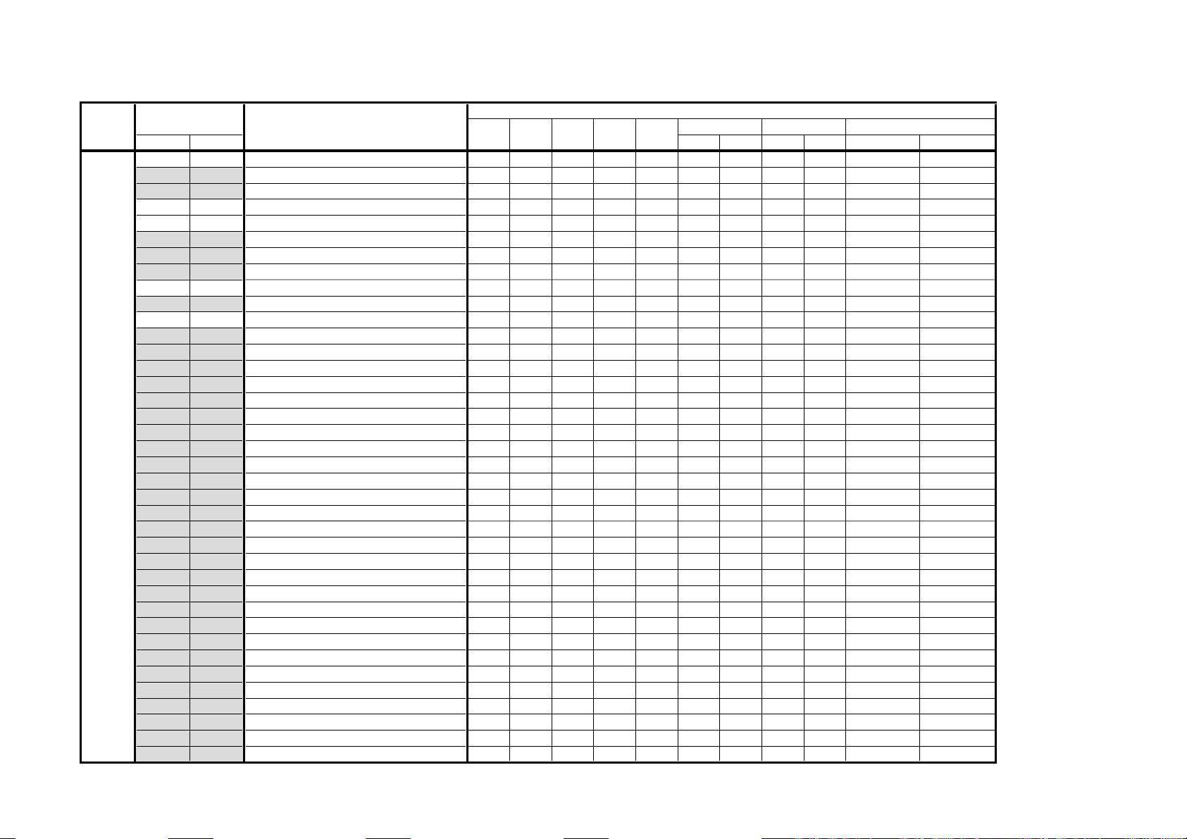
Category
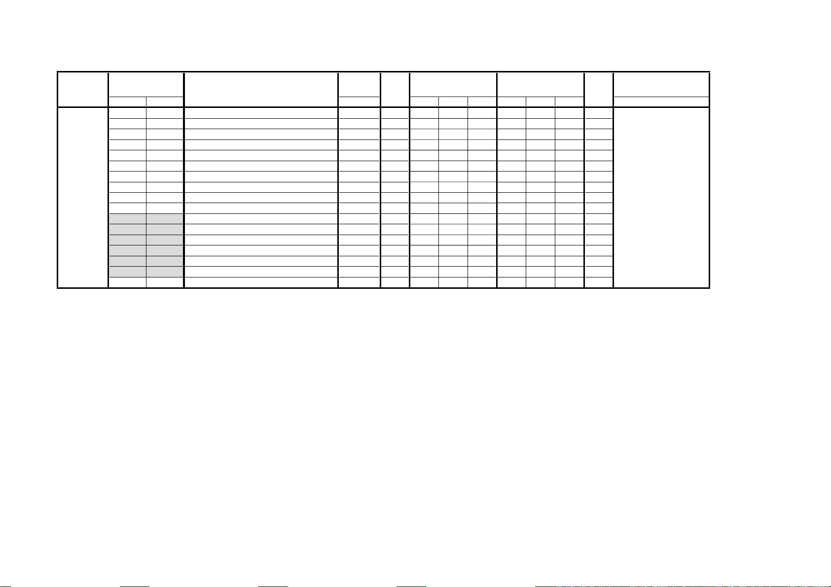
GE3 00 HBL
– 23 –
GE4 00 DFS
Item
No. Name
01 LBL
02 RBL
03 VBL
04 TBL
05 BBL
06 BLK
07 VCM
08 HCM
09 ACM
0A PCM
0B AFC
0C JMP
0D VSW
0E RST
0F EWD
10 AKT
11 PPL
12 M15
13 HFQ
14 HFX
15 VMP
16 ITL
17 VLL
18 VLH
19 AGC
01
DFH
02 QPH
03 QAM
04 QAV
05 QAA
06 QPC
07 QPV
08 QPP
09 QAM
0A QAV
0B QAA
0C CPY
Function
HORIZONTAL BLANKING SWITCH
LEFT BLANKING
RIGHT BLANKING
VERTICAL BLANKING SWITCH
TOP BLANKING
BOTTOM BLANKING
BLANKING OFF
VERTICAL COMPENSATION
HORIZONTAL COMPENSATION
AFC COMPENSATION
PIN COMPENSATION
AFC LOOP GAIN
REFERENCE PULSE JUMP SWITCH
VERTICAL DRIVE JUMP SWITCH
VERTICAL DRIVE START SWITCH
PIN DC LEVEL SHIFT
AKB TIMING
PIN COMP POLARITY
FH=15K @ MS MODE
Fh setting @multi-scan
Reciprocal Fh @mult-scan
VERTICAL MULTI-SCAN MODE
FREERUN INTERLACE SETTING
VERTICAL # OF LINE(L)
VERTICAL # OF LINE(H)
AGC SW for PAL
DF SW
DF Phase
QP Phase
DQP AMPLITUDE
DQP AMPLITUDE VERTICAL MODULATION
DQP AMPLITUDE TILT
DQP DC LEVEL
DQP DC LEVEL VERTICAL MODULATION
DQP DC LEVEL TILT
DQP AMPLITUDE
DQP AMPLITUDE VERTICAL MODULATION
DQP AMPLITUDE TILT
COPY FUNCTION (Full to Vcomp/normal)
DRC1250
01
3F
17
01
00
00
00
00
00
00
00
03
00
01
00
00
16
00
00
50
19
00
00
00
00
00
11
1F
07
14
3C
07
00
PROGRESSIVE
DRC100 DRC1250 VC PRGRE VC DRC100 VC TWIN INDEX HD
01 01 01 01 01 01 01 01
3F 3F 3F 3F 3F 3F 3F 3F
17 17 17 17 17 17 17 17
01 01 01 01 01 01 01 01
0B 0F OF OF 0F 04 04 0F
0E 0F 0F 0F 0F 08 08 0F
00 00 00 00 00 00 00 00
00 00 00 00 00 00 00 00
00 00 00 00 00 00 00 00
00 00 00 00 00 00 00 00
00 00 00 00 00 00 00 00
03 03 03 03 03 03 03 03
00 00 01 01 01 00 00 01
01 01 01 01 01 01 01 01
00 00 00 00 00 00 00 00
00 00 00 00 00 00 00 00
16 09 09 09 10 16 16 09
00 00 00 00 00 00 00 00
00 00 00 00 00 00 00 00
50 50 50 50 50 50 50 50
19 19 19 19 19 19 19 19
00 00 00 00 00 00 00 00
00 00 00 00 00 00 00 00
00 00 00 00 00 00 00 00
00 00 00 00 00 00 00 00
00 00 00 00 00 00 00 00
11 11 11 11 11 11 11 11
1F 1F 1F 1F 1F 1F 1F 1F
07 07 07 07 07 07 07 07
14 14 14 14 14 14 14 14
3C 3C 3C 3C 3C 3C 3C 3C
07 07 07 07 07 07 07 07
00 00 00 00 00 00 00 00
Standard Data
50 Hz
Device Name
(Slave Address)
CXA2170AQ(86H)
KP-FX43M31/M61/M91
KP-FX53M31/M61/M91
RM-998
Page 24
Standard Data
Category Function
No. Name
GE3 00 HBL
– 24 –
GE4 00 DFS
01 LBL LEFT BLANKING 3F 3F 3F 3F 3F 3F 3F 3F 3F 3F
02 RBL RIGHT BLANKING 17 17 17 17 17 17 17 17 17 17
03 VBL VERTICAL BLANKING SWITCH 01 01 01 01 01 01 01 01 01 01
04 TBL TOP BLANKING 00 06 0A 0C 0C 0F 04 04 0C 04
05 BBL BOTTOM BLANKING 00 08 0E 00 00 0F 06 06 0B 06
06 BLK BLANKING OFF 00 00 00 00 00 00 00 00 00 00
07 VCM VERTICAL COMPENSATION 00 00 00 00 00 00 00 00 00 00
08 HCM HORIZONTAL COMPENSATION 00 00 00 00 00 00 00 00 00 00
09 ACM AFC COMPENSATION 00 00 00 00 00 00 00 00 00 00
0A PCM PIN COMPENSATION 00 00 00 00 00 00 00 00 00 00
0B AFC AFC LOOP GAIN 03 03 03 03 03 03 03 03 03 03
0C JMP REFERENCE PULSE JUMP SWITCH 00 00 00 01 01 01 00 00 01 00
0D VSW VERTICAL DRIVE JUMP SWITCH 01 01 01 01 01 01 01 01 01 01
0E RST VERTICAL DRIVE START SWITCH 00 00 00 00 00 00 00 00 00 00
0F EWD PIN DC LEVEL SHIFT 00 00 00 00 00 00 00 00 00 00
10 AKT AKB TIMING 10 10 09 12 12 10 09 09 09 09
11 PPL PIN COMP POLARITY 00 00 00 00 00 00 00 00 00 00
12 M15 FH=15K @ MS MODE 00 00 00 00 00 00 00 00 00 00
13 HFQ Fh setting @multi-scan 50 50 50 50 50 50 50 50 50 50
14 HFX Reciprocal Fh @mult-scan 19 19 19 19 19 19 19 19 19 19
15 VMP VERTICAL MULTI-SCAN MODE 00 00 00 00 00 00 00 00 00 00
16 ITL FREERUN INTERLACE SETTING 00 00 00 00 00 00 00 00 00 00
17 VLL VERTICAL # OF LINE(L) 00 00 00 00 00 00 00 00 00 00
18 VLH VERTICAL # OF LINE(H) 00 00 00 00 00 00 00 00 00 00
19 AGC AGC SW for PAL 00 00 00 00 00 00 00 00 00 00
01
02 QPH QP Phase
03 QAM DQP AMPLITUDE
04 QAV DQP AMPLITUDE VERTICAL MODULATION
05 QAA DQP AMPLITUDE TILT
06 QPC DQP DC LEVEL 00 00 00 00 00 00 00 00 00 00
07 QPV DQP DC LEVEL VERTICAL MODULATION 00 00 00 00 00 00 00 00 00 00
08 QPP DQP DC LEVEL TILT 00 00 00 00 00 00 00 00 00 00
09 QAM DQP AMPLITUDE 00
0A QAV DQP AMPLITUDE VERTICAL MODULATION 19
0B QAA DQP AMPLITUDE TILT 1B
0C CPY COPY FUNCTION (Full to Vcomp/normal) 00
HORIZONTAL BLANKING SWITCH 01 01 01 01 01 01 01 01 01 01
DF SW
DFH
DF Phase
DRC1250 PROGRE DRC100 DRC1250 VC PROGRE DRC100 VC TWIN INDEX HD MS-MODE
00
19
1B
00
00
19
1B
00
00
19
1B
00
60 Hz
00
19
1B
00
00
19
1B
00
00
19
1B
00
00
19
1B
00
00
19
1B
00
00
19
1B
00
Device NameItem
(Slave Address)
CXA2170AQ(86H)
KP-FX43M31/M61/M91
KP-FX53M31/M61/M91
RM-998
Page 25
WHB 00 YOS
DC Offset Canceller for Y Signal 07
CXA2170AQ(86H)
01 UOS
DC Offset Canceller for Cb Signal 1F 1F 27 27 1F 27 27 1F
02 VOS
DC Offset Canceller for Cr Signal 1F 1F 29 29 1F 29 29 1F
03 SBR
Sub Brightness Control 1F
04 RDR
R Drive 1F
05 GDR
G Drive 17
06 BDR
B Drive 1F
07 RCT
R Cutoff 1F
08 GCT
G Cutoff 1B
09 BCT
B Cutoff 1F
0A SBO
Sub Brightness Offset 1F
0B RDO
R Drive Offset 1F
0C GDO
G Drive Offset 1F
0D BDO
B Drive Offset 1F
0E RCO
R Cutoff Offset 1F
0F GCO
G Cutoff Offset 1F
10 BCO
B Cutoff Offset 1F
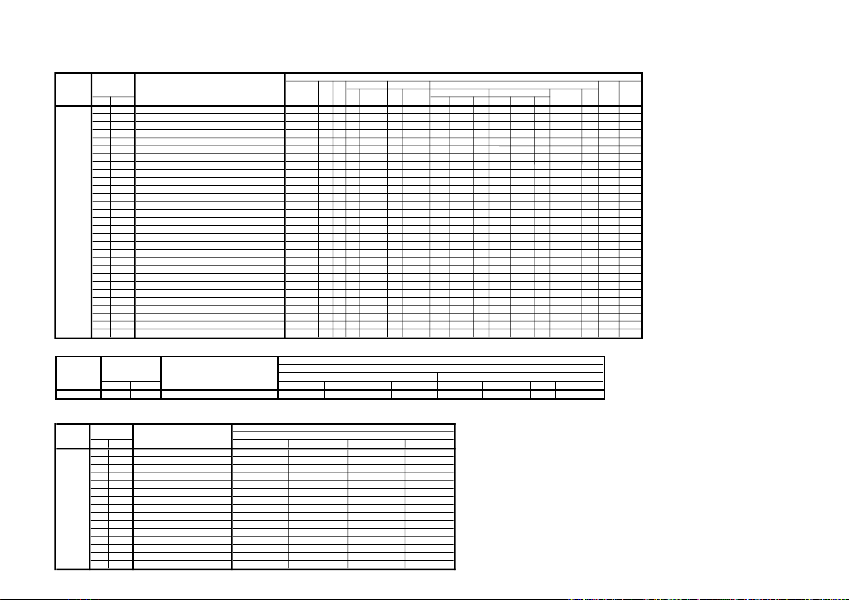
Category
Item
No. Name
Function
NVM
Address
Common SD-I SD-P HD SD-I SD-P HD
Others
YUV
RGB
MS
Device Name
(Slave Address)
– 25 –
*YUV, RGB : Component Signal
SD-I : 480i, 576i
SD-P : 480P, 576P
HD : 720P, 1080i (50/60 Hz)
KP-FX43M31/M61/M91
KP-FX53M31/M61/M91
RM-998
Page 26
– 26 –
Standard Data
Category
Item
Function
Picture Mode
No. Name Dynamic
Standard Hi-Fine Psesonal
SAJ 00 PIC
Picture Control
3F 32 25 80%
01 BRT
Brightness Control
21 1F 1F 50%
02 COL
Color Control 53":30 / 43":2D 53":2A / 43":27 53":22 / 43":1F
03 HUE
Hue Control
1F 1F 1F 50%
04 SHP
Sharpness Control
22 1F 1D 50%
05 VML
VM Level
06 DYC
Dynamic Color on/off
01 01 00 01
07 WBS
White Balance Offset Setting
00 00 00 00
0C GMS
Gamma Shape Correction
07 07 00 07
0D GMR
Gamma Red
07 03 00 07
0E GMG
Gamma Green
07 03 00 03
0F GMB
Gamma Blue
07 03 00 03
10 DCT
DC Transmission Control
06 03 00 03
11 APL
Auto Pedestal Level Control
01 02 00 02
12 ABM
ABL Mode Control
02 02 00 02
Standard Data
Category
Item
Function Common
50 60 50 60
Input Node Table Group 2 Twin Index
YUV RGB OTHER MS
No. Name TV VIDEO TV VIDEO SD-I SD-P HD SD-I SD-P HD
SAJ 00 PIC
Picture Control
*1
01 BRT
Brightness Control
*1
02 COL
Color Control
*1
03 HUE
Hue Control
*1
04 SHP
Sharpness Control
*1
05 VML
VM Level
*1
06 DYC
Dynamic Color on/off
*1
07 WBS
White Balance Offset Setting
*1
08 RYR
Color Matrix Specification
0D 08
09 RYB
Color Matrix Specification
0F 09
0A GYR
Color Matrix Specification
07 09
0B GYB
Color Matrix Specification
04 06
0C GMS
Gamma Shape Correction
*1
0D GMR
Gamma Red
*1
0E GMG
Gamma Green
*1
0F GMB
Gamma Blue
*1
10 DCT
DC Transmission Control
*1
11 APL
Auto Pedestal Level Control
*1
12 ABM
ABL Mode Control
*1
13 ABT
ABL Current detection Vth Control
*2
14 CLO
Color Offset
15 CLW
Color Step Width to the Change of S/N
03
16 HUO
Hue Offset
17 SHO
Sharpness Offset
18 SHW
Sharpness Step Width to the Change of S/N
02
19 PIO
Picture Offset for TWIN/INDEX
07 07
1A BRO
Brightness Offset
0F 06 06 0F 06 06 0F
1B DPL
APED BLACK SIZE INFLECTED SETTING
00
1C TCO
COLOR ON/OFF SETTING
00
SAJ: Standard Data *1
Category
No. Name
SAJ 13 ABT
SAJ: Standard Data *2
Item Function ECO Mode
ABL Current detection Vth Control 53":08/46":0B 53":04/46":07
Standard Data
V-Comp Twin/Index WD-N Other(4:3) V-Comp Twin/Index WD-N Other(4:3)
Eco Off Eco On
-
53":04/46":07
53":0B/46":0E 53":08/46":0B
-
53":08/46":0B
KP-FX43M31/M61/M91
KP-FX53M31/M61/M91
RM-998
Page 27
Category
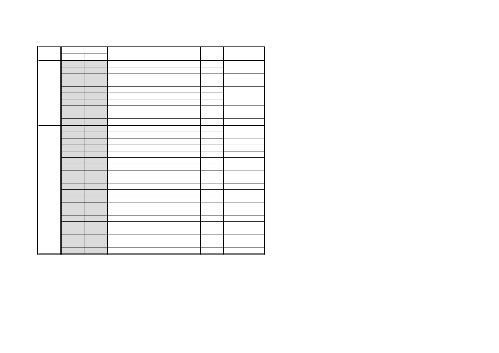
DCN 00 SHS
LDG 00 NSC
– 27 –
Item
No. Name Common
DC AMP3
01 YBU
02 YBL
03 RAP
04 RUB
05 RLB
06 LAP
07 LUB
08 LLB
09 CAJ
01 EWC
02 LX
03
04 HST
05 ENS
06 TES
07 NSS
08 EWS
09 NSG
0A EWG
0B ENG
0C ENS
0D TLD
0E TLU
0F TLL
10 TRD
11 TRU
12 TRL
13 DHM
VCA9
VCA10
DC AMP2
VCA5
VCA6
DC AMP1
VCA1
VCA2
DC AMP4
NS Correction
EW Correction
Left Cross Correction
RX
Right Cross Correction
H Shift Correction
Environmental SW
Temperature SW
NS SW
EW SW
NS Correction Gain
EW Correction Gain
Environmental Correction Gain
NS Correction by Environment
Temp. Corr. DC of Left side
Temp. Corr. DC of Left side
Temp.Corr. Gain of Left Upper
Temp. Corr. Gain of Left Lower
Temp. Corr. Gain of Right Upper
Temp. Corr. Gain of Right Lower
DH Mute
Function
Data
Range
Standard Data
00
00
00
00
00
00
00
00
00
00
00
00
00
00
00
00
00
00
00
00
00
00
00
00
00
00
00
00
00
00
KP-FX43M31/M61/M91
KP-FX53M31/M61/M91
RM-998
Page 28
Category
Item
No. Name
JGL 00 PON RGB and AKB Reference Pulse Output On/Off
– 28 –
01 RGB RGB Output Selection
02 AGG Aging Mode Selection
03 BBT RGB Bottom Limitter Control
04 LML RGB Amplitude Limitter Control
05 SCO Sub Picture Control
06 LEV RGB Level for RGB
07 SYS Signal Band Selection
08 SF0 Sharpness f0 setting
09 SF1 High f0 sharpness gain control
0A PRO Pre/Over-Shoot Ratio Control
0B LTI Luminance Transient Improvement
0C LTM LTI Mode Setting
0D CTI Chrominance Transient Improvement
0E VDL VM OUT Phase Control
0F VCR VM OUT Coring Level Setting
10 VFO VM OUT F0 Setting
11 VLM VM OUT Limiter Level Setting
12 SPH H Sync Delay Timing Setting
13 CLP CLP Pulse Phase Control
14 CLG CLP Pulse Gate Setting
15 CLS CLP Pulse Start Phase Setting
16 YOS DC_OFFSET RANGE FOR Y SIGNAL SETTING
17 YLT Y AMPLITUDE LIMITER LEVEL SETTING
18 YCS Y SIGNAL GAIN SETTING
19 PHA PHASE ADJ
1A AKO AKB_OFF
1B HBS RGB OUTPUT H BLANKING WHEN AKBOFF=0
1C ARG
AUTO REGI LRGB_LEV
Function 50
Common
01
07
00
00
00
05
01 01 01 01 01 01 01 01 01 01 01 01
01
00
03
00
00
00
03
03
00
00
53":0C / 43":07
TV VIDEO TV VIDEO
07 07 07 07 07 07 07 07 07 07 03
01 01 01 01 01 02 03 01 02 03 03
00 01 00 01 01 01 03 01 01 03 00
03 03 03 03 03 03 03 03 03 03 03
08 07 0A 07 07 07 0F 07 07 0F 07
00 00 00 00 00 00 00 00 00 00 00
02 02 02 02 02 02 02 02 02 02 02
03 03 03 03 03 03 00 03 03 00 00
01 01 01 01 01 01 01 01 01 01 00
60 Picture Mode
SD-I SD-P HD SD-I SD-P HD
Standard Data
RGBYUV
MS
Dynamic Standard Hi-Fine Personal
02 02 00 02
01 01 00 01
KP-FX43M31/M61/M91
KP-FX53M31/M61/M91
RM-998
Page 29
Sharpness Center Frequency Changing
02
Cb/Cr Output Level Control
1A
BPF/TQF Switch
01
SECAM Gate Position Adjustment
00
25 WCO
Cb/Cr Output Level Step for noise reduction
00
Category Function
Standard Data
1F1F
00 00
53":07 / 43":05
YCT 00 TNT Tint Adjustment for NTSC
– 29 –
Item
No. Name
01 PNG PAL/NTSC Gate Width
02 PNI PAL/NTSC Sensitivity SW
03 SCL Sub Color Control
04 SCT Sub Contrast Control
05 SF0
06 SEQ Sharpness Equalizer Characteristic
07 SHG Sharpness Gain Control
08 YOL Y-output Level Control
09 BSP Black Stretch Start Point Changing
0A COL
0B DCR DC Restoration Ratio Adjustment
0C BF0 BPF/TQF F0 Adjustment
0D BFQ BPF/TQF Q Adjustment
0E FSW
0F SDT SECAM Double Trap Switch
10 LPF Y/Cb/Cr LPF Switch
11 YDL Y-DL Time Adjustment
12 B01 Cb Offset1 Adjustment (main route)
13 RO1 Cr Offset1 Adjustment
14 CDF V Count Down Frequency Switch
15 CDM V Count Down Judge Switch
16 AFC AFC Sensitivity Switch
17 MVM Macrovision Mask + AFC Mask
18 SRY SECAM R-Y Black Adjustment
19 SBY SECAM B-Y Black Adjustment
1A BEL SECAM BELL/HPF Switching
1B BLF BELL f0 Adjustment
1C SVI SECAM V -ID Switch
1D SGP
1E SID SECAM Sensitivity Switch
1F SIH SECAM Inhibition Switch
20 STP Y Black Level Setup for PAL plus
21 ASW AUTO SWITCH
22 3NR 3D NR Operation on/off
23 BW6 3D NR for 60Hz non-bust signal on/off
24 WSH Sharpness Gain Step for noise reduction
othersS-Input3DComb2DCombCommon
01
00
03
1F
00
00
00
02
01
01
06 05 05 03
0A
07
00
00
00
07
01
02
00
00
01
00
00
01
01
01
00
TV
50TV 60TV 50Video 60Video 50DVD 60DVD
1F 1F
07 07 07 07
07 07 07 07
07 06 05 06
53":07 / 43":05
00 00
DVDVIDEO
KP-FX43M31/M61/M91
KP-FX53M31/M61/M91
RM-998
Page 30
Sharpness Equalizer Characteristic
03
Macrovision Mask + AFC Mask
00
SECAM B-Y Black Adjustment
01
Category
TV
Video
SYC 00 TNT
– 30 –
Item
No. Name
01 PNG
02 PNI
03 SCL
04 SCT
05 SF0
06 SEQ
07 SHG
08 YOL
09 BSP
0A COL
0B DCR
0C BF0
0D BFQ
0E FSW
0F SDT
10
11 YDL
12 NCM
13 B01
14 RO1
15 CDF
16 CDM
17 AFC
18 MVM
19 SRY
1A SBY
1B BEL
1C BLF
1D SVI
1E SGP
1F SID
20 SIH
21 STP
22 ASW
LPF
Function
Tint Adjustment for NTSC
PAL/NTSC Gate Width
PAL/NTSC Sensitivity SW
Sub Color Control
Sub Contrast Control
Sharpness Center Frequency Changing
Sharpness Gain Control
Y-output Level Control
Black Stretch Start Point Changing
Cb/Cr Output Level Control
DC Restoration Ratio Adjustment
BPF/TQF F0 Adjustment
BPF/TQF Q Adjustment
BPF/TQF Switch
SECAM Double Trap Switch
Y/Cb/Cr LPF Switch
Y -DL Time Adjustment
1-H Addition Switch
Cb Offset1 Adjustment (main route)
Cr Offset1 Adjustment
V Count Down Frequency Switch
V Count Down Judge Switch
AFC Sensitivity Switch
SECAM R-Y Black Adjustment
SECAM BELL/HPF Switching
BELL f0 Adjustment
SECAM V-ID Switch
SECAM Gate Position Adjustment
SECAM Sensitivity Switch
SECAM Inhibition Switch
Y Black Level Setup for PAL plus
SUB AUTO SWITCH
S-InputCommon DVD
01
00
02
07
1F
00
1F
00
01
02
01
01
01
05 03 03 03
01
07
07
00
00
07
02
00
00
00
01
00
00
01
COLOR MODE
SECAM NTSC PAL 50 60 50 60
Standard Data
1F 1F
07 07 07 07
07 07 07 07
1F
1F
00
00
00
KP-FX43M31/M61/M91
KP-FX53M31/M61/M91
RM-998
Page 31

Category
SYN 00 MAT Matrix Conversion
– 31 –
Item
No. Name
01 VFR Dummy Sync Freq
02 SL1 Input Signal Type for IN1
03 SL2 Input Signal Type for IN2
04 FSY Sync Identification Mode
05 VTC V sync Separation Time Constant
06 HWD Output Pulse Width
07 HSL Sync Separation Mode
08 HTC H-Sync Separation Time Constant
09 HSW YG Out signal Output
0A HMA Hsync within V sync
0B MAC Macrovision
0C DUM Out dummy sync or signal sync
0D CLK Clock Select
0E GSL Gain Select
0F CBG CB Gain
10 CRG CR Gain
11 YG Y Gain
12 HFR
Dummy Frequency Select
Function
Table Input Siganl
fh15k 525i, 625i
otherfh 525p, 625p, 1080i/50 Hz, 1080i/60 Hz, 720p/50 Hz, 720p/60 Hz
DVD 525i, 525p, 625i, 625p
HD 1080i/50 Hz, 1080i/60 Hz, 720p/50 Hz, 720p/60 Hz
RGB Don't care DVD or HD
Common fh15k otherfh DVD HD RGB
01
00
01
01
00
00
01
00
00
00
07
07
07
01
Standard Data
00 01 03
03 03 01
03 00
00 01
01 00
KP-FX43M31/M61/M91
KP-FX53M31/M61/M91
RM-998
Page 32

2C 17 00
NICAM Prescale 7F
Category
AP 00 BBS
MSP 00 WST
– 32 –
No. Name
01 BCB
02 SBS
03 BCT
04 STS
05 AGL
06 BSW
07
08
09
01 WBT
02 WLL
03
04 WDL
05 NDL
06 SDL
07 AGC
08 REL
09 CRM
0A ACO
0B FP
0C FPM
0D FH
0E FHM
0F WGP
10 NIP
11 ERR
12 VOL
BAS
TRE
BBE
WAC
Bass Boost Setting 00
Boost/Cut Sub-Bass 01
Sub-Bass Setting 03
Boost/Cut Sub-Treble 01
Sub-Treble Setting 01
AGC Level Setting 00
Bass Boost Switch 00
Bass sound mode Control
Treble sound mode Control
BBE Sound mode Control
W/G Stereo Threshold 15
W/G Bilingual Threshold EC
W/G Monaural Threshold 05
W/G Agreement Count 01
W/G Search Delay 30
NICAM Search Delay 20
Stereo status Read Delay 10
AGC Switch Auto/Constant 01
AGC Gain at Constant Mode 28
Carrier muting on/off 00
Audio Clock out on/off 01
FM Prescale for non-M system 1B
FM Prescale for M system 32
FM Prescale for HDEV 36
FM Prescale for HDEV and M 65
W/G Prescale 1C
Auto FM switch Threshold 50
Loud Speaker gain 0700h to 07FFh 30
Function
Common Dynamic Drama Soft
(Model : 43")
(Model : 53")
(Model : 43")
(Model : 53")
(Model : 43")
(Model : 53")
Standard DataItem
19 14 01
17 14 04
12 00 04
01 11 03
24 23 00
Device Name
(Slave Address)
BD3886FS
MSP3415D(84H)
KP-FX43M31/M61/M91
KP-FX53M31/M61/M91
RM-998
Page 33

Threshold of Green Enhancement switch
07
Green Enhancement Gain
00
Green Enhancement Width
00
Category
LTI 00 LDH
– 33 –
Item
No. Name
01 CFS
02 WLB
03 VDC
04 DEM
05 CDP
06 OSP
07 WPO
08 DSK
09 ASK
0A WSK
0B SSK
0C DGR
0D DGT
0E GGR
0F WGR
10 SGR
11 DBL
12 GBL
13 SBL
14
15 CST
16 CTI
17 BON
18 BTD
19 NLD
1A NLW
1B VGD
1C VGW
1D PKD
1E PKW
1F SPD
20 CRD
21 CRW
22 CRO
23 LWD
24 SNM
25 SNC
26 FMC
CDS
Function
Histogram segment Selection
Contour Filter Selection
Letterbox Window Switch
Video Dependent Coring
Demonstration Mode
Luminance Delay
Overrule Smart Peaking
White Point Stretch Off
Skin T one Switch
Skin Tone Angle Selection
Skin T one Width Selection
Skin Tone Size selection
Green Enhancement switch
Green Enhancement Size
Blue Stretch Switch
Blue Stretch Gain Selection
Blue Stretch Size selection
Color Dependent Sharpness
Threshold of Color Dependent Sharpness
Color T ransient Improvement
Black offset Compensation
Adaptive Black Strecth
Non-Linearity Amplifier
Step Width of Non-Linearity Amplifier
Variable Gamma
Step Width of Variable Gamma
Peaking Amplitude
Step Width of Peaking Amplitude
Steepness Correction
Coring Level
Step Width of Coring Level
Coring Level Offset for Video Mode
Line Width Correction
S/N Mode under unreliable S/N condition
S/N Ratio Average Counter
Feature Mode Matching Counter
Common Twin TV Video Dynamic Standard Hi-Fine Personal
01
01
00
00
04
00
00
00
00
00
00 01 01 00 01
00
00
00
00
07
00 1D 13 05 13
04
1F 22 15 1A 15
00
08
09
09
1F
01
02
Standard Data
03 03
01 01 01 01
00 00 00 00
01 01 01 01
00 00 00 00
00 00 00 00
00 00 00 00
32 32 1D 32
00 00 00 00
1B 1B 0F 1B
KP-FX43M31/M61/M91
KP-FX53M31/M61/M91
RM-998
Page 34

Item Standard Data
No. Name 480i/576i Others Twin Scroll / Index
06 YCD 0 0 0 0
Item Standard Data
No. Name Table 0 (1920dots) Table 1 (1920dots) Table 2 (1920dots) Table 3 (1920dots)
07 DYSD 3333
Item
Standard Data
No. Name 4:3Model 16:9Model
All Normal Others
08 MHP 00 98 00
0A MHS F0 A2 F0
Category
Functionality
Function
No. Name
MD1 00 HAP
01 VAP
02 HAS
03 VAS
04 HPW
05 VPW
06 YCD
07 YSD
08 MHP
09 MVP
0A MHS
0B MVS
0C MPH
0D MPV
0E SHP
0F SVP
10 SHS
– 34 –
MD2 00 HAP
11 SVS
12 PHP
13 PVP
14 PHZ
15 PVZ
16 DPS
17 MDS
18 BCL
19 YST
01 HAS
02 VAP
03 VAS
H active Display area phase
V active Display area phase
h active display area size
v active display area size
display h pulse width
display v pulse width
display output yc signal delay correct
display output ys signal delay correct
main display picture h position
main display picture v position
main display picture h size
main display picture v size
multi picture mode h position
multi picture mode v position
sub display picture h position
sub display picture v position
sub display picture h size
sub display picture v size
PinP Large mode h position
PinP Large mode v position
PinP Large mode h size
PinP Large mode v size
display pll switch
model select
background Color y
Display output ys signal type select
DRC H-Active Area Position
DRC H-Active Area Size
DRC V-Active Area Position
DRC V-Active Area Size
Standard
Data
*1
*1
*1
*1
*1
*1
*2
*3
*4
*5
*4
*5
*6
*6
A7
05
73
4F
00
00
00
00
*7
*8
*9
1
*1
*1
*1
*1
MD1: Standard Data *1
Item Standard Data
No. Name Other 1152i/576p / 1080i/50Hz 480i/120Hz 576i/100Hz
00 HAP 69 69 69 69
01 VAP 14
02 HAS F0 F0 F0 F0
03 VAS 87 90 87 90
04 HPW 36 36 36 36
05 VPW 05 05 03 03
3F F 22
MD1: Standard Data *2
MD1: Standard Data *3
MD1: Standard Data *4
KP-FX43M31/M61/M91
KP-FX53M31/M61/M91
RM-998
Page 35

MD1: Standard Data *5
Item Standard Data
No. Name TV / 4:3Model PJ / 4:3Model PJ / 16:9Model
Single MS Others Single MS Others Single MS Others
18 BCL 0 0 0 005 5 05
Item Standard Data
No. Name 1080i other
16 DPS 0 0
Item Standard Data
No. Name Normal (16:9Model) V comp (4:3Model) other
60Hz 50Hz 60Hz 50Hz 60Hz 50Hz
RF,CV,S-Video YPbPr RF,CV,S-Video YPbPr RF,CV,S-Video YPbPr RF,CV,S-Video YPbPr RF,CV,S-Video YPbPr RF,CV,S-Video YPbPr
00 HAP A1 A0 B2 B1 84 83 95 94 84 83 95 94
01 HAS A2 A2 9F 9F B2 B2 AF AF B2 B2 AF AF
02 VAP 24 24 30 30 29 29 35 35 24 24 30 30
03 VAS 78 78 90 90 6E 6E 84 84 78 78 90 90
Item Standard Data
No. Name Twin - Left Scroll / Index -Main
60Hz 50Hz 60Hz 50Hz
RF,CV,S-Video YPbPr RF,CV,S-Video YPbPr RF,CV,S-Video YPbPr RF,CV,S-Video YPbPr
00 HAP 95 95 A1 A0 A1 A0 B1 B0
01 HAS A5 A5 A3 A3 A2 A2 A0 A0
02 VAP 38 38 3F 3F 36 36 3F 3F
03 VAS 6E 6E 86 86 6F 6F 86 86
Item Standard Data
No. Name Single Single(V Comp)
60Hz 120Hz 50Hz 100Hz 60Hz 120Hz 50Hz 100Hz
960i/480p 1080i/540p 480i 1152i/576p 1080i (4:3 Model) 1080i (16:9Model) 576i 960i/480p 480i 1152i/576p 576i
09 MVP 1E 0 0F 0 27 0E 023126 3
0B MVS 78 87 3C 90 7B 87 48 6E 37 84 42
MD1: Standard Data *8
Item Standard Data
No. Name 4:3 Model 16:9 Model
17 MDS 8 9
MD1: Standard Data *6
Item Standard Data
No. Name 60Hz 50Hz 60Hz 50Hz
TWIN Twin Index (4:3 Model) Scroll (16:9Model) Index (4:3 Model) Scroll (16:9Model)
0C MPH 1C 1C 3C 1F 3D 20
0D MPV C 6 3E 1E 22 24
MD1: Standard Data *7
– 35 –
MD2: Standard Data *1
MD1: Standard Data *9
KP-FX43M31/M61/M91
KP-FX53M31/M61/M91
RM-998
Page 36

Item Standard Data
No. Name 60Hz 50Hz
480i (RF,CV,S-Video) 480p 1080I 720p 576i (RF,CV,S-Video) 576p 1080i 720p
04 VOP 1 0 0 0 0 0 0 0
05 CLM 42 7A 48 42 4C 7B 48 58
06 CPW 2 3 3 3 2 3 3 3
07 YCD 0 0 0 0 0 0 0 0
Item Standard Data
No. Name 60Hz 50Hz
480i (RF,CV,S-Video) 480p 1080I 720p 576i (RF,CV,S-Video) 576p 1080i 720p
08 PSP 3E 81 8B BA 4D 9B 8B BA
09 PST 0 0 0 0 0 0 0 0
Category
Functionality
Function
No. Name
MD3 00 HAP
01 HAS
02 VEP
03 VLS
04 VOP
05 CLM
06 CPW
07 YCD
08 PSP
09 PST
0A HSC
0B REV
MD4 00 HAP
01 HAS
02 VLP
03 VLS
04 CPT
– 36 –
05 CPW
06 YCD
07 PSP
08 PST
VDO H-Active Area Position
VDO-H active Area pixel size
VDO-V active even position
VDO-V active area line size
VDO-V active odd position
VDO-Clamp pulse output timing
VDO-Clamp pulse width
VDO-Analog input yc delay correct
VDO-external pll pd stop line count
VDO-external pll pd start line count
VDO-H sync cycle
VDO-Field reverse
DTV H active area position
DTV H active area size
DTV V active area line position
DTV V active area line size
DTV Clamp pulse output timing
DTV Clamp pulse width
DTV analof input yc correct
DTV external pll pd stop line count
DTV external pll pd start line count
Standard
Data
*1
*1
*1
*1
*2
*2
*2
*2
08
8B
00
82
70
F0
13
87
50
04
00
00
00
MD3: Standard Data *1
Item Standard Data
No. Name Normal (16:9Model) V comp (4:3Model) Other Scroll / Index -Sub Twin - Right
480p / 60Hz 576p / 50Hz 480p / 60Hz 576p / 50Hz 60Hz 50Hz 60Hz 50Hz 60Hz 50Hz
480p 1080i 720p 576p 1080i (4:3 Model)
00 HAP BE CB 9C AA 9C 6E 8B AA 6E 6E 8B 8B 96 A7 9C AA
01 HAS DD DD F0 F0 F0 F0 1 F0 F0 F0 A1 A1 A5 A2 A7 A5
02 VEP 25 2F 2A 34 25 15 1B 2A 15 15 35 27 1B 1E 1A 1E
03 VLS 78 90 6E 84 78 87 B4 7B 87 87 A4 B4 37 43 37 43
1080i (16:9Model) 720p (4:3 Model) 720p (16:9Model) TV, CV, S-Video
KP-FX43M31/M61/M91
KP-FX53M31/M61/M91
MD3: Standard Data *2
MD3: Standard Data *3
RM-998
Page 37

Category
Functionality
Function
Standard
Data
No. Name
MD5 00 POP
01 MHY
02 MHC
03 MVY
04 MVC
05 MHR
06 MHL
07 MHE
08 MHO
09 MCR
0A MCL
0B MCE
0C MC0
0D MYR
0E MYL
0F MYE
10 MVR
– 37 –
11 MVL
12 MVE
13 SHY
14 SHC
15 SVY
16 SVC
17 SHR
18 SHL
19 SHE
1A SHO
1B SCR
1C SCL
1D SCE
1E SC0
1F SYR
20 SYL
21 SYE
22 SVR
23 SVL
24 SVE
Service Data Effect
Main H LPF Y Coefficient Code
Main H LPF C Coefficient Code
Main V LPF Y Coefficient Code
Main V LPF C Coefficient Code
Main h enhance y coring code
Main h enhance y cliping code
Main h enhance y level code
Main h enhance y coefficient code
Main h enhance c coring code
Main h enhance c cliping code
Main h enhance c level code
Main h enhance c coefficient code
Main V enhance y coring code
Main v enhance y cliping code
Main v enhance y level code
Main V enhance c coring code
Main V enhance c cliping code
Main V enhance c level code
sub h LPF y coefficient Code
sub h LPF c coefficient Code
sub v LPF y coefficient Code
sub v LPF c coefficient Code
sub h enhance y coring code
sub h enhance y cliping code
sub h enhance y level code
sub h enhance y coefficient code
sub h enhance c coring code
sub h enhance c cliping code
sub h enhance c level code
sub h enhance c coefficient code
Sub V enhance y coring code
sub v enhance y cliping code
sub v enhance y level code
Sub V enhance c coring code
Sub V enhance c cliping code
Sub V enhance c level code
*1
*1
*1
*1
*1
*1
*1
*1
*1
*1
*1
*1
*1
*1
*1
*1
*1
*1
*1
00
00
00
00
00
00
00
00
00
00
00
00
00
00
00
00
00
00
KP-FX43M31/M61/M91
KP-FX53M31/M61/M91
RM-998
Page 38

MD5: Standard Data *1
Item Standard Data
No. Name POP=00 POP=01 POP=02 POP=03 POP=04 POP=05 POP=06 POP=07 POP=08 POP=09 POP=0A POP=0B POP=0C POP=0D POP=0E POP=0F
01MHY1 111 1 1 1 1 11111111
02MHC3 333 3 3 3 3 33333333
03MVY0 000 0 0 0 0 00000000
04MVC0 000 0 0 0 0 00000000
05MHR2 101 2 1 0 1 21112111
06MHL1 101 1 1 0 1 11111111
07MHE5 303 5 3 0 3 53555355
08 MHO 0 0 0 53":1 / 43":0 0 0 0 0 0 1 0 0010
09MCR2 202 2 2 0 2 22222222
0AMCL1 101 1 1 0 1 11111111
0BMCE0 000 0 0 0 0 00000000
0CMCO0 000 0 0 0 0 00000000
0DMYR2 101 2 1 0 1 21112100
0EMYL1 101 1 1 0 1 11111111
0F MYE 1 0 1 53":3 / 43":1 1 0 1 1 1 3 2 1132
10MVR2 202 2 2 0 2 22222222
11MVL1 101 1 1 0 1 11111111
– 38 –
12MVE0 000 0 0 0 0 00000000
Dynamic Standard Hi-Fine Personal Dynamic Standard Hi-Fine Personal Dynamic Standard Hi-Fine Personal Dynamic Standard Hi-Fine Personal
53":1 / 43":0
53":3 / 43":1
576i RF/Composite 480i RF/Composite 576i RF/Composite Normal Mode (Wide model only) 480i Component Normal mode (Wide model only)
MD5: Standard Data *2
Item Standard Data
No. Name POP=10 POP=11 POP=12 POP=13 POP=14 POP=15 POP=16 POP=17 POP=18 POP=19 POP=1A POP=1B POP=1C POP=1D POP=1E POP=1F
01 MHY 1 1 2 1 1 1 2 1 1 1 1 1 1 1 1 1
02 MHC 3 3 3 3 3 3 3 3 3 3 3 3 3 3 3 3
03 MVY 0 0 0 0 0 0 0 0 0 0 0 0 0 0 0 0
04 MVC 0 0 0 0 0 0 0 0 0 0 0 0 0 0 0 0
05 MHR 2 1 0 1 2 1 0 1 2 1 1 1 2 1 1 1
06 MHL 1 1 0 1 1 1 0 1 1 1 1 1 1 1 1 1
07 MHE 5 3 0 3 5 3 0 3 5 3 7 5 5 3 7 5
08 MHO
09 MCR 2 2 0 2 2 2 0 2 2 2 2 2 2 2 2 2
0A MCL 1 1 0 1 1 1 0 1 1 1 1 1 1 1 1 1
0B MCE 0 0 0 0 0 0 0 0 0 0 0 0 0 0 0 0
0C MCO 0 0 0 0 0 0 0 0 0 0 0 0 0 0 0 0
0D MYR 2 1 0 1 2 1 0 1 2 1 1 1 2 1 1 1
0E MYL 1 1 0 1 1 1 0 1 1 1 1 1 1 1 1 1
0F MYE 53":5 / 43":3 1 0 1 1 0 1 1 1 3 2 1 1 3 2
10 MVR 2 2 0 2 2 2 0 2 2 2 2 2 2 2 2 2
11 MVL 1 1 0 1 1 1 0 1 1 1 1 1 1 1 1 1
12 MVE 0 0 0 0 0 0 0 0 0 0 0 0 0 0 0 0
Dynamic Standard Hi-Fine Personal Dynamic Standard Hi-Fine Personal Dynamic Standard Hi-Fine Personal Dynamic Standard Hi-Fine Personal
53":1 / 43":0
576i Component 480i Component 576i Composite Normal Mode (Wide model only) 480i RF/Composite Normal Mode (Wide model only)
010 010 0 0 1 1 0 0 1 1
53":1 / 43":0
53":5 / 43":3
KP-FX43M31/M61/M91
KP-FX53M31/M61/M91
RM-998
Page 39

MD5: Standard Data *3
Item Standard Data
No. Name POP=20 POP=21 POP=22 POP=23 POP=24 POP=25 POP=26 POP=27 POP=28 POP=29 POP=2A POP=2B POP=2C POP=2D POP=2E POP=2F
576i 100 Hz (for All Input) 480i 120 Hz (for All Input) 576p 480p
Dynamic Standard Hi-Fine Personal Dynamic Standard Hi-Fine Personal Dynamic Standard Hi-Fine Personal Dynamic Standard Hi-Fine Personal
01MHY1121 1 1 2 1 11111111
02MHC3333 3 3 3 3 33333333
03MVY0000 0 0 0 0 00000000
04MVC0000 0 0 0 0 00000000
05MHR2101 2 1 0 1 32023202
06MHL1101 1 1 0 1 12021202
07MHE5303 5 3 0 3 44044404
08 MHO 1/0 0 0 0 1/0 0 0 0 1 1 1 1 1 1 1 1
09MCR2202 2 2 0 2 20002000
0A MCL 1 1 0 1 1 1 0 1 0 0 0 0 0 0 0 0
0B MCE 0 0 0 0 0 0 0 0 0 0 0 0 0 0 0 0
0CMCO0000 0 0 0 0 11111111
0DMYR2101 2 1 0 1 22022202
0E MYL 1 1 0 1 1 1 0 1 1 1 0 1 1 1 0 1
0F MYE 3/1 1 0 1 3/1 1 0 1 3 3 0 3 3 3 0 3
10MVR2202 2 2 0 2 00000000
– 39 –
11MVL1101 1 1 0 1 00000000
12MVE0000 0 0 0 0 01010101
MD5: Standard Data *4
Item Standard Data
No. Name POP=30 POP=31 POP=32 POP=33 POP=34 POP=35 POP=36 POP=37 POP=38 POP=39 POP=3A POP=3B POP=3C POP=3D POP=3E POP=3F
1080i 50/60Hz 720p 50/60Hz P&P / Index / Scroll Memory Stick
Dynamic Standard Hi-Fine Personal Dynamic Standard Hi-Fine Personal Dynamic Standard Hi-Fine Personal Dynamic Standard Hi-Fine Personal
01MHY0000000000002222
02MHC2222222200003333
03MVY0000000000000000
04MVC0000000000000000
05MHR2202220200001111
06MHL1101110100001111
07 MHE 5/2 1 0 1 2 1 0 1 0 0 0 0 4 2 5 3
08MHO0111111100001111
09MCR3202320200002222
0AMCL2202220200001111
0BMCE2202220200000000
0CMCO1111111100000000
0DMYR2202220200002111
0EMYL1101110100001111
0FMYE7313331300001132
10MVR3202320300002222
11MVL1101110100001111
12MVE3202320300000000
KP-FX43M31/M61/M91
KP-FX53M31/M61/M91
RM-998
Page 40

Item Standard Data
No. Name VDO 480i/576i other
00 MCON 31 27
01 SCOR 128 128
02 SCOG 128 147
03 SCOB 128 147
04 RGB 0 0
MD6: Standard Data *1
Category
Functionality
No. Name
MD6 00 MCT
01 MWH
02 MWV
03 MHP
04 MVP
05 MHS
06 MVS
MD7 00 MCN
01 SCR
02 SCG
03 SCB
04 RGB
Function
Main Cut Out on
Main Write H size
Main Write V size
Main Read H position
Main Read V Position
Main Read H Size
Main Read V Size
Main Contrast
Sub Contrast R
Sub Contrast G
Sub Contrast B
RGB OUT Select
Standard
Data
0
*1
*1
*1
*1
*1
– 40 –
KP-FX43M31/M61/M91
KP-FX53M31/M61/M91
RM-998
Page 41

Y Blanking level adjustment 00
Category
Item
No. Name
3NR 00
01
02
03
04
05
06
07
08
09
0A
0B
0C
0D
0E
0F
10
– 41 –
11
12
13
14
15
16
17
18
19
1A
1B
1C
1D
1E
1F
PLL Divider setting(PAL=47, NTSC=44)
WHC
NIQ U/V input polarity 01
CLW A/D Clamp Pulse width 1E 1E
CLP A/D Clamp Pulse Phase 10 10
YBW Y H Blanking width 8A 8A
YBL
YBO Internal Y H Blanking ON/OFF 00
MUT Signal Output Muting 00
YBS Y H Blanking start point 28 28
CBW U/V H Blanking width 8A 8A
CBS U/V H Blanking start point 28 28
CBO Internal U/V H Blanking ON/OFF 00
VBL V H Blanking level adjustment 00
UBL U H Blanking level adjustment 00
CDL U/V output delay 00 00
YDL Y output delay 00 00
PVI VD input polarity 00
PHI HD input polarity 00
HDW HD pulse width 10
PVO VD output polarity 00
PHO HD output polarity 00
HST HD out pulse start position 36
VDL VD out Pulse start position 00
VDW VD out Pulse width 03
NDE Noise detection point 00
NVP Noise detect line 02
NDS Noise detect sencitivity 03
HOF H Reference pulse ON/OFF (ON=0) 01
NDW Noise detect gate width 09
UOS U Offset level 00
POT Output Port 0/1 Control 00 01
UVF UV Frag polarity 00
Function
2F 2C
6050Common
NR0 NR1 NR2 NR3 NR0 NR1 NR2 NR3
Standard Data
OTHER COLOR SYSTEMNTSC
KP-FX43M31/M61/M91
KP-FX53M31/M61/M91
RM-998
Page 42

Y NR level 00 08 0C 0E 04 08 0C 0E
Y Moving detection gain 00 00 00 00 00 00 00 00
Category
Item
No. Name
3NR 20
21
22
23
24
25
26
27
28
29
2A
2B
2C
2D
2E
2F
30
– 42 –
31
32
33
34
35
36
37
38
39
3A
3B
3C
APC AP Clock polarity 01
DAP DAC power save (ON=1) 00
YLV
YST Y Standard detection off/on 00
YNT Y NTSC Standard detection 01
YPL Y PAL Standard detection 01
YMV Y Moving detection filter (ON=0) 00
YCR Y Moving detection Coring level 00 00 07 0A 00 00 07 0A
VOS V Offset level 00
YMG
YEG Y Moving detect on (ON=1) 01
YEL Y edge moving detection sensitivity 03 04 03 03 03 04 03 03
YLM Y NR Feed back limit level 00 03 04 08 02 03 04 08
CLV C NR level 00 08 09 0B 04 08 09 0B
CNT Relate C NR to YSTDN 01
CPL Relate C NR to YSTDP 01
CMG C Moving detection gain 00 00 00 00 00 00 00 00
CCR C Moving detection level 00 00 06 0C 00 00 06 0C
CLM C NR Feed back limit level 00 04 05 05 00 04 05 05
NVS NR Vertical start line 14 14
NHS NR Horizontal start position 10 10
NVE NR Vertical end line (offset:+100d) D2 A0
NHE NR Horizontal end position 78 78
YNG Y Coring gain 01 01
COR Coring/through (Coring=0) 00 00
LPF LPF on/off (on=0) 00
Y Coring limit level
YLT
YNC Y Coring offset level 00 08 0C 0E 04 08 0C 0E
YCO Y Coring off (on=1) 01 01
Function
00 00
6050Common
NR0 NR1 NR2 NR3 NR0 NR1 NR2 NR3
Standard Data
OTHER COLOR SYSTEMNTSC
KP-FX43M31/M61/M91
KP-FX53M31/M61/M91
RM-998
Page 43

External C-sync Input Selection
01
DY Detection Gain Adjustment
0A 0A 0A 0A
Category
Item
No. Name
3CM 00 NRM
01 YCO
02 SYC
03 STD
04 MSS
05 KIL
06 ECS
07 CPP
08 HDP
09 CDL
0A DYC
0B DYG
0C DCC
0D DCG
0E YNR
0F CNR
10 WSC
– 43 –
11 VTH
12 VTR
13 LDR
14 VAP
15 VAI
16 YPF
17 YPG
18 VSE
19 CCN
1A COS
1B SDC
1C SDY
1D YHC
1E YHG
1F SHT
20 CLK
21 PLL
22 KRF
23 HSL
24 VSL
25 BPS
26 BPW
27 ADC
28 APD ADC Power-down Switch
29 SPD
Noise Reduction Operation Mode
Y/C Signal Output Selection
System Clock Selection
Standard/Non-standard Operation Selection
Inter-frame/Inter-line Operation Selection
Killer/Non-killer Operation Selection
ADC Input Level & Clump Pulse Width Selection
Horizontal Phase Adjustment
C-signal delay Adjustment
DY Detection Coring Level Adjustment
DC Detection Coring Level Adjustment
DC Detection Gain Adjustment
YNR Non-linear Filter Setup
CNR Non-linear Filter Setup
Noise Detectin Coring Adjustment
Hysteresis Selection for H-sync Non-standard
Sensitivity Selection for H-sync Non-standard
Sensitivity Selection for Frame-sync Non-standard
Gain Adjustment for Vertical Shape Correction
Vanishing Adjustment for Vertical Shape Correction
Center Frequency Selection for Y-peaking BPF
Gain Adjustment for Y-peaking BPF
Line Comb Filter Setup
C-signal Split Filter Switch
C-signal Delay Switch at Noise Reduction
DC Detection Sensitivity Switch
DY Detection Lower-level Sensitivity Switch
Y-signal Higher-level Coring Selection
Y-signal Higher-level Gain Switch
Non-standard Detection & H/V Counter Test Bits
Clock T est Bits
PLL Filter Setup
Killer Detection Reference Adjustment
H-sync Slice Level Adjustment
V-sync Slice Level Adjustment
Internal Burst Gate Start Position Adjustment
Internal Burst Gate Width Adjustment
ADC Clock Delay Selection
Memory Power-down Switch
Function NR Mode Picture Morde
00
0D
01
00
00
00
00
05
04
01
01
01
02
00
00
00
01
00
08
0D
03
0C
08
04
0A
03
01
00
VideoTVCommon
01 01
01 01
02 01
NRmode0 NRmode1 NRmode2 NRmode3 Dynamic Standard Hi-Fine Personal
02 02 02 04
05 03 03 05
05 0A 0A 05
Standard Data
00 00 00 00
00 00 00 00
03 03 03 03
0A 08 08 08
00 00 00 00
00 00 00 00
KP-FX43M31/M61/M91
KP-FX53M31/M61/M91
RM-998
Page 44

No.
Name
DRC100 DRC1250 Progressive HD1080i
DRC100 DRC1250 Progressive HD1080i
(Slave Address)
2CM
00
FUN
Function
03
TC90A69 (B2H)
01
YCM
Y/C separator
00
02
CNR
CNR K
00
03
LIM
CNR limit
00
04
CPF
C-LPF
00
05
SLP
SelC-LPF
00
06
YFO
Y-P fo
00
07
YPG
Y-EQ Gain
00
08
YPL
Y-EQ/ N.C Limit
00
09
CLP
Pds.Clip
00
0A
YPF
Y-LPF
00
0B
VEG
V-Emph gain
03
0C
VEN
V-Emph N.L
03
0D
VEC
V-Emph Core
01
TXT
00
TXH
Teletext Horizontal Display Position
29
SAA5264(58H)
01
TXV
Teletext Vertical Display Position
27
02
THD
Teletext H-sync Active Edge Shift
00
03
TVD
Teletext V-sync Active Edge Shift
00
04
HPL
Teletext H-sync Polarity Configuration
01
05
VPL
Teletext V-sync Polarity Configuration
00
06
FPL
Teletext V-sync Polarity Configuration
01
07
FMD
Teletext Fastext/TOP Force Mode
02
08
TBR
Teletext RGB Brightness
03
0A
TCH
Teletext Twisted Character Set Configuration
OSD
00
OSH
OSD H Position
0D
CXP961F064(60H)
01
OSV
OSD V Position
25
3F
3F
3D
1B
30
30
30
02
FW1
OSD ODD/EVEN Field Window Setup #1
07
03
FW2
OSD ODD/EVEN Field Window Setup #2
14
Category
Device Name
Common
60 Hz
50 Hz
Standard Data
Function
Item
– 44 –
09
04
NOP
Teletext National Option Table Configuration
OHO
OSD H Position Offset for INDEX
01(M31/M61)
02(M91)
01(M31/M61)
02(M91)
04
KP-FX43M31/M61/M91
KP-FX53M31/M61/M91
RM-998
Page 45

Category : PJE
ITEM ITEM Contents min max 625(100Hz) 625(50Hz) 1125(50Hz) 1125(60Hz) 525(120Hz) 525(60Hz)
No. Name Full Zoom Vcomp Widezoom Full Zoom Vcomp Widezoom Full Vcomp Full Vcomp Full Zoom Vcomp Widezoom Full Zoom Vcomp Widezoom
0 FDIS Switch of display for fine adjustment data 0 1 1
1 AREA Area setting 0 2 0
2 COPY Service copy adjustment 0 1 0
3 ALCP Service all copy adjustment 0 1 0
4 OSDH Osd horizontal position of PJED service menu 1 255 11
5 OSDV Osd vertical position of PJED service menu 1 255 28 56 34 45 1 1 1 1 1 1 15 28 17 42 21 28 57 106 65 78
6 FVSL Start position of fine adjustment 0 15 15 14 1 15 15 14 1 15 15 1 0 1 15 14 1 15 0 14 1 15
7 FVSP Start line of fine adjustment 0 255 31 9 7 1 64 20 16 4 64 16 53 73 29 9 11 11 3 21 25 25
8 V1DL Value of V1 delay 0 255 8 88 8 58 17 175 17 116 17 17 1 1 1 72 1 32 1 140 1 61
9 V1CU Value of V1 count up 0 4095 763 998 577 895 387 506 292 454 387 292 387 292 895 1179 665 998 454 598 337 506
10 V1OH Value of V1 offset upper data 0 255 7 7 130 7 5 5 128 5 5 128 79 184 7 7 135 7 5 5 134 5
11 COHP Horizontal phase for rough adjustment 0 4095 0
12 FIHP Horizontal phase for fine adjustment 0 4095 1111
13 TPHP Horizontal phase for test pattern 0 4095 72
14 TPVP Vertical phase for test pattern 0 255 38 70 39 58 72 136 74 112 72 74 15 17 30 58 29 42 55 111 53 79
15 DFHP Horizontal phase for dynamic focus(4:3) 0 4095 250
16 DFHG Horizontal parabola wave for dynamic focus(4:3) -128 127 -70 -65 -70 -65 -70 -65 -70 -65 -65 -70 -70 -70 -70 -65 -70 -65 -70 -65 -70 -65
17 DFVG Vertical parabola wave for dynamic focus(4:3) -128 127 -90 -90 -128 -90 -90 -90 -128 -90 -90 -128 -128 -128 -90 -90
18 DFDC Center for dynamic focus -128 127 127 127 127 127 127 127 127 127 127 127 127 127 127 127
19 DFV1 V1 saw wave for dynamic focus -128 127 -60 -50 -60 -50 -20 -50 -20 -50 -50 -40 -40 -40 -90 -50 -90 -50 -40 -50 -40 -50
20 SDHP Compensation of horizontal phase for shading 0 4095 500
– 45 –
21 SDH1 Horizontal saw wave for shading(4:3) -128 127 63 127 127 127 63 127 127 127 63 127 63 127 63 127 127 127 63 127 127 127
22 BDVU Vartical positioni for boder line 1 0 2047 6 4 4 0 11 9 7 0 45 41 45 41 10 8 12 3 20 15 24 6
23 BDVL Vartical positioni for boder line 2 0 2047 538 412 536 464 1077 823 1073 928 1044 1040 1044 1040 454 344 456 413 908 689 912 826
24 BDHL Horizontal position for boder line 1 0 2047 152 152 152 145 152 152 152 145 152 152 152 152 152 152 152 145 152 152 152 145
25 BDHR Horizontal position for boder line 2 0 2047 1254 1254 1254 1261 1254 1254 1254 1261 1254 1254 1254 1254 1254 1254 1254 1261 1254 1254 1254 1261
26 HBLD Horizontal phase for output of H.Blank out 0 4095 32
27 HBLW Width for output of H.Blank out 0 4095 143
28 PWM2 PWM2 output width setting of Regi IC 0 4095 43": 500/ 53": 345
29 R0GH Green Horizontal Sensor 0 Ratio Offset -128 127 0 0
30 R0RH Red Horizontal Sensor 0 Ratio Offset -128 127 0 0
31 R0BH Blue Horizontal Sensor 0 Ratio Offset -128 127 0 0
32 R1GH Green Horizontal Sensor 1 Ratio Offset -128 127 0 0
33 R1RH Red Horizontal Sensor 1 Ratio Offset -128 127 0 0
34 R1BH Blue Horizontal Sensor 1 Ratio Offset -128 127 0 0
35 R1GV Green Vertical Sensor 1 Ratio Offset -128 127 0 0
36 R1RV Red Vertical Sensor 1 Ratio Offset -128 127 0 0
37 R1BV Blue Vertical Sensor 1 Ratio Offset -128 127 0 0
38 R2GH Green Horizontal Sensor 2 Ratio Offset -128 127 0 0
39 R2RH Red Horizontal Sensor 2 Ratio Offset -128 127 0 0
40 R2BH Blue Horizontal Sensor 2 Ratio Offset -128 127 0 0
41 R2GV Green Vertical Sensor 2 Ratio Offset -128 127 0 0
42 R2RV Red Vertical Sensor 2 Ratio Offset -128 127 0 0
43 R2BV Blue Vertical Sensor 2 Ratio Offset -128 127 0 0
44 R3GH Green Horizontal Sensor 3 Ratio Offset -128 127 0 0
45 R3RH Red Horizontal Sensor 3 Ratio Offset -128 127 0 0
-128
-90 -90 -90 -128 -90
127
127 127 127 127 127
KP-FX43M31/M61/M91
KP-FX53M31/M61/M91
RM-998
Page 46

ITEM ITEM Contents min max 625(100Hz) 625(50Hz) 1125(50Hz) 1125(60Hz) 525(120Hz) 525(60Hz)
No. Name Full Zoom Vcomp Widezoom Full Zoom Vcomp Widezoom Full Vcomp Full Vcomp Full Zoom Vcomp Widezoom Full Zoom Vcomp Widezoom
46 R3BH Blue Horizontal Sensor 3 Ratio Offset -128 127 0 0
47 PTRH Red Horizontal Top Pattern Position Offset -128 127 0 0
48 PTBH Blue Horizontal Top Pattern Position Offset -128 127 0 0
49 PLRH Red Horizontal Left Pattern Position Offset -128 127 0 0
50 PLBH Blue Horizontal Left Pattern Position Offset -128 127 0 0
51 PLRV Red Vertical Left Pattern Position Offset -128 127 0 0
52 PLBV Blue Vertical Left Pattern Position Offset -128 127 0 0
53 PRRH Red Horizontal Right Pattern Position Offset -128 127 0 0
54 PRBH Blue Horizontal Right Pattern Position Offset -128 127 0 0
55 PRGV Green Vertical Right Pattern Position Offset -128 127 0 0
56 PRRV Red Vertical Right Pattern Position Offset -128 127 0 0
57 PRBV Blue Vertical Right Pattern Position Offset -128 127 0 0
58 PBGH Green Horizontal Bottom Pattern Position Offset -128 127 0 0
59 PBRH Red Horizontal Bottom Pattern Position Offset -128 127 0 0
60 PBBH Blue Horizontal Bottom Pattern Position Offset -128 127 0 0
61 ERR Auto Regi. Error code 0 - 0 0
62 ADTM A/D data input timing of Auto Regi. 0 255 97 81
63 ADT2 A/D Timing 2 0 255 133 115
64 SZLM Size Limit -128 127 0 0
65 RTLM Ratio Limit 0 127 80 80
66 VUP Auto Regi. Pattern Upper vertical position 0 2047 43": 60/ 53": 60 43": 41/ 53": 41
67 VMID Auto Regi. Pattern Middle vertical position 0 2047 43": 605/ 53": 605 43": 505/ 53": 505
68 VLOW Auto Regi. Pattern Lower vertical position 0 2047 43": 1153/ 53": 1153 43": 971/ 53": 971
– 46 –
69 HLE Auto Regi. Pattern left horizontal position 0 4095 43": 55/ 53": 55 43": 55/ 53": 55
70 HMID Auto Regi. Pattern middle horizontal position 0 4095 43": 636/ 53": 636 43": 636/ 53": 636
71 HRIV Auto Regi. Pattern right horizontal position 0 4095 43": 1217/ 53": 1217 43": 1217/ 53": 1217
72 TEST Auto regi. Pattern display switch 0 1 0
73 SFTF Switch of shift fast 0 1 0
74 SFTE Switch of shift enable 0 5 4
75 ACTL Acount timer counter lower byte 0 - 0
76 ACTH Acount timer counter upper byte 0 - 0
77 ATTN Sensor level attenuation sw 0 1 43": 0/ 53": 0
78 VB1S Start position of VBLKOUT1 0 1023 0 0 0 0 0 0 0 0 0 0 0 0 0 0 0 0 0 0 0 0
79 VB1W Width of VBLKOUT1 0 1023 8 8 8 8 16 16 16 16 16 16 16 16 8 8 8 8 16 16 16 16
80 VB2S Start position of VBLKOUT2 0 1023 0 0 0 0 0 0 0 0 0 0 0 0 0 0 0 0 0 0 0 0
81 VB2W Width of VBLKOUT2 0 1023 32 65 40 49 60 127 78 95 77 94 20 37 27 56 35 36 50 107 65 68
82 VB3S Start position of VBLKOUT3 0 1023 315 282 307 298 628 561 610 593 611 594 554 537 264 235 257 255 524 467 509 506
83 VB3W Width of VBLKOUT3 0 1023 22 55 31 39 47 114 65 82 64 81 8 26 17 46 25 26 39 96 54 57
84 VB4S Start position of VBLKOUT4 0 1023 0 0 0 0 78 134 91 113 78 91 7 7 0 0 0 0 0 0 0 0
85 VB4W Width of VBLKOUT4 0 1023 5 5 5 5 5 5 5 5 5 5 5 5 5 5 5 5 5 5 5 5
KP-FX43M31/M61/M91
KP-FX53M31/M61/M91
RM-998
Page 47

Note: Coarse Adjustment is prepared for each screen mode. 4:3
Adjustment Limit
CENT
H35±170
V20±170
SIZE H max : - 75
LIN
H (Blue) min : - 425
H (Red) max : 425
Green Blue Red
ADJUSTMENT min max H V H V H V
85 CENT
86 SKEW
87 SIZE
88 LIN
89 KEY
90 PIN
91 MLIN
92 MSIZ
Coarse Adjustment -512 511 35 20 35 20 35 20
Coarse Adjustment -512 511 000000
Coarse Adjustment -512 511 -100 -75 -100 -75 -100 -75
Coarse Adjustment -512 511 0 0 -410 0 410 0
Coarse Adjustment -512 511 0 0 0 -120 0 120
Coarse Adjustment -512 511 0 300 0 300 0 300
Coarse Adjustment -512 511 0 0 145 0 -145 0
Coarse Adjustment -512 511 0 0 0 0 0 0
– 47 –
KP-FX43M31/M61/M91
KP-FX53M31/M61/M91
RM-998
Page 48

APC Switch
01
Enable Noise Reduction in Video Mode
00
RF Signal Change Counter after Locked
0F
Category
OPM 00 COM Comb Operation Selection
– 48 –
OPB 00 OP1 Optional Bits 1 (see the specified sheet)
Item
Function
No. Name
01 APC
02 TSY
03 MUT No Signal Mute
04 AFM Auto FM switch
05 TVO V-Angle correction to Picture Rotation
06 DBL Disable Blueback function
07 SSO Speed CH Search Selection
08 SCH CH Selection for Shipping Condition
09 SCA Cable/Air Selection for Shipping Condition
0A DMG Disable Menu-operation Guide
0B VSN
0C RUC RF Signal Change Counter after Unlocked
0D RLC
0E LBB Lower Blue Back Intensity
0F 23P 2/3 Pull Down Mode 0: Force OFF, 1: Auto
10
01 OP2 Optional Bits 2 (see the specified sheet)
02 OP3
TV System Selection under searching with Auto TV System
MS Background color to gray
Optional Bits 3 (see the specified sheet)
Common
00
00
00
01
00
01
01
01
01
00
0F
00
01
FB
17
05
DRC100 DRC1250 Progressive HD1080i DRC100 DRC1250 Progressive HD1080i
Standard Data
60 Hz50 Hz
Device Name
(Slave Address)
Option Misc
Option-Bits
KP-FX43M31/M61/M91
KP-FX53M31/M61/M91
RM-998
Page 49

x
x
x
x
3-12. REGISTRATION ADJUSTMENT
3-12-1.ADJUSTMENT FLOW
START
KP-FX43M31/M61/M91
KP-FX53M31/M61/M91
RM-998
3-12-2. Setup for Adjustment
1. Marking
1) At the 4 insides of the screen, locate the middle. Use a tape
measure to identify the middle.
Turn on the power and wait for 10 minutes
Set to the PAL Full mode
Check the deflection yokes, the centering magnets, 2 pole/4 pole magnets
Set to the service mode
MAIN DEFLECTION ADJUSTMENT ( Green)
Green coarse adjustment
2
Green fine adjustment
Red coarse adjustment
Change the
display mode
Red fine adjustment
SUB DEFLECTION
ADJUSTMENT
X : midlle
3-12-3. Method of Main Deflection Adjustment
1. Place the caps on the red and blue lenses so that only the green
color is displayed.
2. Enter the PAL SPCB signal, and set the DRC1250.
3. Set in the Service mode, and select the category “GE1” ,
“GE2”.
4. Adjust “00 VPS” in “GE1” so that the picture is displayed in
the center of screen.
00 VPS
Blue coarse adjustment
5. Adjust “01 VSZ” in “GE1” and “02 HSZ” “GE2” so that the
picture size is within the specification.
Blue fine adjustment
01 VSZ
YES
ALLCOPY*
< Caution >
Before adjustment registration, set PWM2 Data in PJE
service mode as following.
Another display mode ?
NO
Memorize the FLASH FOCUS offset data
50 Hz and 60 Hz
End
02 HSZ
SPECIFICATION : Overscan Spec. = 0.9%
Input Signal H SIZE V SIZE
PAL MONOSCOPE 14.7 ± 0.1 sq. 11.2 ± 0.1 sq.
43" model.......890
53" model.......315
– 49 –
Page 50

6. Write “VPS, VSZ and HSZ” adjusted data to other mode
service data.
<Write “VPS”,“VSZ”,“HSZ”>
DRC1250
(50 Hz)
DRC100
(50 Hz)
DRC1250
V Comp
(50 Hz)
DRC100
V Comp
(50 Hz)
HD
(50 Hz)
DRC1250
(60 Hz)
DRC120
(60 Hz)
DRC1250
V Comp
(60 Hz)
DRC120
V Comp
(60 Hz)
HD
(60 Hz)
TWIN
(60 Hz)
KP-FX43M31/M61/M91
KP-FX53M31/M61/M91
1. Functions of Keys on Commander
• 1 : Changes adjustment item. (item No. moves up)
: Marker moves clockwise from center to outside.
(in fine adjustment mode)
• 4 : Changes adjustment item.
(item No. moves down)
: Marker moves counterclockwise from outside to
center. (in fine adjustment mode)
•
(move) :Marker moves up, down, or to the left or right.
• 3 : Changes adjustment color.
• 6 : Displays or changes internal test signals.
• 9 : Switches adjustment mode.
•
(push) (in fine adjustment mode)
: Changes data value.
(up, down, or to the left or right)
(in fine adjustment mode)
(except item No. 00~38) GRN c BLU c RED
: crosshatch + external signal c dot + external sig-
nal c crosshatch only c dot only c off
carsor adjustment mode y fine adjustment
mode
: Switches marker moving method.
joystick key c 1 and 4 buttons
RM-998
3-12-4. Operation Method for Projector Engine
(PJE) Mode
VIDEO
Up : Data up (V)
Write data
to NVM
Adjustment item
up
Adjustment item
down
Read data from
NVM
DRC-MF
P
R
N
I
O
W
G
T
T
HD/DVD
+
–
G
W
O
I
R
N
P
INDEX
PROG
123
456
7809
PROG
A/B
JUMP
Left : Data up (H)
Down : Data down (V)
Right : Data down (H)
Push : Enter
MENU
Copy data to all
mode
Color change
Internal test signal
Initialize data
(Not stored)
Mode select
(Fine carsor)
Commander Function (PJE mode)
Button Mode Description
+ - WRITE Writes data to NVM.
7 + - READ Reads data from NVM.
5 + - *PJE INITILIZED ALL DATA.
INITIAL
2 + - *PJE Copies and writes data of DRC1250
COPY
(50Hz) mode to all other modes.
* : only data in the PJE mode.
2. Operation Method for Rough Adjustment
1) Set in the Service mode, and select the category “PJE”.
2) Press “1” or “4” button on the commander to select the
item, and move “ ” up, down, or to the left or right to
change the data.
PJE 00 00 60
FDIS |
Adjustment Item
Item No.
Data
V-Frequency
OPTION RESET
RM-998
TV
3) Select item “GRN CENT”. When BLU or RED is displayed,
press “3” button on the commander to change the adjustment
color in the order of GRN c BLU c RED.
– 50 –
Page 51

4) In the GRN, BLU, or RED mode, move “ ” up or down to
CROSSHATCH
Movement when joystick key
is moved up.
change the data in vertical direction, or move “
” to the left
or right to change the data in horizontal direction.
Color
GRN 000 000 60
CENT
Adjustment Item
Data (H)
Data (V)
V-Frequency
5) When it moves from PJE to other categories, repeat “1” or
“4” button and press it.
3. Operation Method for Fine Adjustment
(in GRN, RED, or BLU Mode)
1) Set in the Service mode, and select the category “PJE”.
2) Select item “FDIS” so that the data at each position can be
displayed in the fine adjustment mode, and set the data to
“01”.
3) Press “9” button on the commander, and the fine adjust-
ment mode will be active where a green marker appears in
the center of screen (in the case of GRN mode).
4) Push “
switched between green (GRN mode) and white alternately.
5) Use “1” or “4” button on the commander, or the joystick
to move the marker to the position to be adjusted, where fine
adjustment can be made.
• When marker color is white.
(in this case, fine adjustment is disabled)
(ENTER)” button, and the marker color will be
Operating the joystick can move the marker
up, down, or to the left or right freely.
KP-FX43M31/M61/M91
KP-FX53M31/M61/M91
RM-998
• Fine adjustment can be made on the basis of marker position
using joystick key.
Movement when joystic key
is moved to the right.
CROSSHATCH
6) Press “9” button on the commander to return to the rough
adjustment mode.
3-12-5. Method of Projector Engine Adjustment
(Sub Deflection Adjustment)
Adjustment a : Yes – : No
Adjustment Type
Adjustment Item GRN RED BLU
H / V H / V H / V
CENT a / aa / aa / a
SKEW a / aa / aa / a
SIZE a / aa / aa / a
LIN a / aa / aa / a
KEY – / a – / a – / a
PIN a / aa / aa / a
MLIN a / – a / – a/ –
MSIZ a / – a / – a / –
1. Green Adjustment
1) Place the caps on the red and blue lenses so that only the
green color is displayed.
2) Enter the monoscope signal to set.
3) Set in the Service mode, and select the category “PJE”.
4) Press “6” button on the commander to display internal test
signal (crosshatch).
5) Select “GRN CENT”, and adjust so that the picture coincide
in the center of screen.
• GRN CENT (horizontally/vertically)
• When marker color is green. (GRN mode)
1 : moves the marker clockwise from center to outside.
4 : moves the marker counterclockwise from outside to center.
– 51 –
Move the joystick
to the right.
Move the joystick
up.
Move the joystick
to the left.
Move the joystick
down.
Page 52

Move the joystick
to the right.
Move the joystick
to the left.
Move the joystick
to the right.
Move the joystick
to the left.
Move the joystick
up.
Move the joystick
down.
6) Select “GRN SKEW”, and correct the tilt of horizontal lines
and vertical lines.
KP-FX43M31/M61/M91
KP-FX53M31/M61/M91
RM-998
9) Select “GRN MSIZ”, and correct the space intervals for the
horizontal section of the screen are equal.
• GRN SKEW (horizontally/vertically)
Move the joystick
to the right.
Move the joystick
up.
Move the joystick
to the left.
Move the joystick
down.
7) Select “GRN SIZE”, and adjust so that each distance from
center to left end and to right end is equal. Adjust so that each
distance from center to top and to bottom is equal.
• GRN SIZE (horizontally/vertically)
Move the joystick
to the right.
Move the joystick
to the left.
• GRN MSIZ (horizontally)
10) Select “GRN MLIN”, and correct the sizes of the horizontal
line at the center of the screen are symmetrical left and right.
• GRN MSIZ (horizontally)
Move the joystick
to the right.
Move the joystick
to the left.
10) Select “GRN PIN”, and adjust so that right and left vertical
lines on the screen become straight .Adjust so that upper and
lower hprizontal lines on the screen become straight
• GRN PIN (horizontally/vertically)
Move the joystick
up.
Move the joystick
down.
8) Select “GRN LIN”, and adjust so that each space at the right
end and at the left end of screen is equal. Adjust so that each
space at the top and at the bottom of screen is equal
• GRN LIN (horizontally/vertically)
Move the joystick
to the right.
Move the joystick
up.
Move the joystick
to the left.
Move the joystick
down.
11) Select “GRN KEY”, and adjust so that upper and lower hori-
zontal lines on the screen become parallel.
• GRN KEY (vertically)
Move the joystick
up.
Move the joystick
down.
12) Press “9” button on the commander to enter the fine ad-
justment mode.
13) Make fine adjustment so that horizontal lines and vertical
lines become straight.
14) Press “9” button on the commander to return to the
coarse adjustment mode.
– 52 –
Page 53

KP-FX43M31/M61/M91
KP-FX53M31/M61/M91
RM-998
2. Red Adjustment
1) Place a cap on the blue lens so that green and red colors are
displayed.
2) Press “3” button on the commander to select RED mode.
3) Adjust the following items so that blue lines overlap with
green lines.
• RED CENT (horizontally/vertically)
• RED SKEW (horizontally/vertically)
• RED SIZE (horizontally/vertically)
• RED LIN (horizontally)
• RED MSIZ (horizontally)
• RED MLIN (horizontally)
• RED PIN (horizontally/vertically)
• RED KEY (/vertically)
4) Press “9” button on the commander to enter the fine adjust-
ment mode.
5) Make fine adjustment so that horizontal lines and vertical
lines overlap with green lines.
6) Press “9” button on the commander to return to the rough
adjustment mode.
3. Blue Adjustment
1) Place a cap on the red lens so that green and blue colors are
displayed.
2) Press “3” button on the commander to select BLUE mode.
3) Hereinafter, use same manner as that of blue adjustment to
adjust so that the red lines overlap with green lines.3.
Blue Adjustment
4. Registration Data Writing
1) Select “ PJE ”service item.
Ex.PJE 00 FDIS
2) Select “ PJE 03 ALCP” change date “ 00” to “ 01” using Joy
Stick Key, Then push “ MUTE” + “ 0” confirm red ALCP
OSD appear.
3) Regi data of DRC1250(PAL) is copied to all other mode.
When ALCP OSD disappear, data copy is finished.
<PJE adjusted DATA ALL COPY>
DRC1250
(50 Hz)
DRC100
(50 Hz)
DRC1250
V Comp
(50 Hz)
DRC100
V Comp
(50 Hz)
HD
(50 Hz)
DRC1250
(60 Hz)
DRC120
(60 Hz)
DRC1250
V Comp
(60 Hz)
DRC120
V Comp
(60 Hz)
HD
(60 Hz)
– 53 –
Page 54

3-13. AUTO CONVERGENCE SETTING
This adjustment must be performed after the registration adjust-
ment was made or after readjustment was made by any reason.
1. Darken the periphery of this set.
2. Receive the 50Hz (PAL) signal.
3. Set in the service mode.
4. Press “
(AUTO CONVERGENCE)” button on the front
panel of the set.
(The offset value is now automatically stored.)
5. Check that no error message appears.
If an error message appears, recheck.
6. Enter the NTSC monoscope signal, and perform the same
steps in the PAL modes respectively.
3-14. BLUE OFFSET ADJUSTMENT
This adjustment must be ending the G2 adjustment .
KP-FX43M31/M61/M91
KP-FX53M31/M61/M91
RM-998
3-15. WHITE BALANCE ADJUSTMENT
1. Enter the monoscope signal.
2. Set in the service mode.
3. Press “MENU” button on the commander to select “A/V
CONTROL” b “PICTURE MODE” b ”ADJUST”.
Adjustment Condition
PICTURE MODE : PERSONAL
PICTURE : 0%
BRIGHT : 50%
If the noise of DCF (Digital Comb Filter) has an effecting
white balance adjustment, change service data as follows
while the adjustment.
OPM 00 COM : 00 t 01
(This time, beginning inspection also should be done under
some condition.)
1. Receive the HD(1080i/60Hz Black) signal into component
in terminal.
2. Set PICTURE 100%, others are normal, DRC1250/60Hz.
3. Adjust with SLN so that the blue reference pulse peak volt-
age of B100 terminal (CN1100) enters into standard.
Item : GE2 03 SLN
BLUE REFERENCE PULSE
(CN1100 B5 B100)
2.2 ± 0.1V
GND (0V)
V
4. Write the adjustment value in the NVM area of each mode
after the adjustment.
DRC1250
(60 Hz)
TWIN
(60 Hz)
DRC100
(60 Hz)
DRC100
V Comp
(60 Hz)
DRC1250
V Comp
(60 Hz)
HD(1080i)
(60 Hz)
DRC1250
(50 Hz)
DRC100
(50 Hz)
DRC100
V Comp
(50 Hz)
DRC1250
V Comp
(50 Hz)
HD(1080i)
(50 Hz)
Adjusting Parameter
Category Item
WHB 03 SBR
04 RDR
06 BDR
07 RCT
09 BCT
4. Adjust “03 SBR” so that 10 IRE section barely grows.
5. Enter the all-white pattern signal.
6. Adjust “07 RCT” and “09 BCT” so as to attain the optimum
white balance.
7. Adjust “03 SBR” so that 100 IRE section barely grows.
8. Adjust “04 RDR” and “06 BDR” so as to attain the optimum
white balance.
9. Repeatedly adjust the white balance for the minimum and
maximum picture setting.
10. Enter the monoscope signal, and select “SAJ 00 PIC”, and set
the data to “00”.
11. Adjust “03 SBR” so that the border between 0 IRE and 10 IRE
becomes distinct.
– 54 –
Page 55

KP-FX43M31/M61/M91
KP-FX53M31/M61/M91
RM-998
3-16. AUTO CONVERGENCE ERROR CODE LIST
If an error code is displayed after the set has been fully adjusted, correctly, plese check the following items : position, tilt and sizing. If
either of these adjustments are off, even slightli, the auto registration pattern will not hit the four sensors properly. This occurs when the
internal generator patterns is being flashed on the screen for the sensor to read. Therefore, auto registration (called auto convergence)
cannot operate properly causing an error code to be displayed. In order for this function to operate properly, correct position, tilt and size
must be adjusted properly.
ERROR CODE LIST
ERROR
CODE
DESCRIPTION NOTE
10 Sensor 0 low output Check sensor 0, connection/Wiring, circuit and pattern position.
(Are patterns hitting sensor ?) Adjust V UP, HMID if necessary.
11 Sensor 1 low output Check sensor 1, connection/Wiring, circuit and pattern position.
(Are patterns hitting sensor ?) Adjust HLE, VMID if necessary.
12 Sensor 2 low output Check sensor 2, connection/Wiring, circuit and pattern position.
(Are patterns hitting sensor ?) Adjust HRIV, VMID if necessary.
13 Sensor 3 low output Check sensor 3, connection/Wiring, circuit and pattern position.
(Are patterns hitting sensor ?) Adjust VLOW, HMID if necessary.
20 Sensor 0 high output Check sensor 0 and circuit.
21 Sensor 1 high output Check sensor 1 and circuit.
22 Sensor 2 high output Check sensor 2 and circuit.
23 Sensor 3 high output Check sensor 3 and circuit.
30 V center or skew adjustment Check VMID data and check registration condition.
loop overflow
31 H center or skew adjustment Check HMID data and check registration condition.
loop overflow
32 H linearity or size adjustment Check HLE and HRIV data and check registration condition.
loop overflow
40 V center regi data overflow
41 H center regi data overflow
42 V skew regi data overflow
43 H skew regi data overflow
44 H linearity regi data overflow
Check VMID data and confirm V center data (all modes) is not near 511.
Check HMID data and confirm H center data (all modes) is not near 511.
Check VMID data and confirm V skew data (all modes) is not near 511.
Check HMID data and confirm H skew data (all modes) is not near 511.
Check HLE data and HRIV data and confirm H center data (all modes)
is not near 511.
45 H size regi data overflow
Check HLE data and HRIV data and confirm H center data (all modes)
is not near 511.
50 V center regi data overflow
51 H center regi data overflow
52 V skew regi data overflow
53 H center regi data overflow
54 H linearity regi data overflow
Check VMID data and confirm V center data (all modes) is not near 512.
Check HMID data and confirm H center data (all modes) is not near 512.
Check VMID data and confirm V skew data (all modes) is not near 512.
Check HMID data and confirm H skew data (all modes) is not near 512.
Check HLE data and HRIV data and confirm H center data (all modes)
is not near 512.
55 H size regi data overflow
Check HLE data and HRIV data and confirm V center data (all modes)
is not near 512.
60 Cent/Skew calibration loop Check HMID and VMID data and check registration condition.
overflow
61 Size/Lin calibration loop Check HLE, HRIV, VUP, and VLOW data and check registration
overflow condition.
70 V cent/Skew ratio limit Check sensors 1 and 2, connection/wiring, circuit, increase RTLM.
71 H cent/Skew ratio limit Check sensors 0 and 3, connection/wiring, circuit, increase RTLM.
73 H size/Lin ratio limit Check sensors 1 and 2, connection/wiring, circuit, increase RTLM.
80 Size limit Error Check that horizontal size data is not near SZLM.
[SENSOR POSITION]
12
0 : UPPER SENSOR
1 : LEFT SENSOR
2 : RIGHT SENSOR
3 : LOWER SENSOR
0
SCREEN
3
• ERROR CODE SCREEN DISPLAY
(When press “ (AUTO CONVERGENCE)” button.)
RORH
R0RH
Horizintal/Vertical
R, G, B
Sensor 0/1/2/3
Ratio Offset
– 55 –
• ERROR CODE SCREEN DISPLAY
(When select “PJE” b “61 ERR”.)
PJE 61 133
ERR |
Category : PJE
Item : 61 ERR
133
Color : (0=G, 1=R, 2=b, 3=ALL)
Error code : (See Error codelist)
Page 56

SECTION 4
SAFETY RELATED ADJUSTMENT
KP-FX43M31/M61/M91
KP-FX53M31/M61/M91
RM-998
4-1. HV REGULATION ADJUSTMENT
When replacing the following components marked with ]
on the schematic diagram, always check hold-down volt-
age and if necessary re-adjust.
[ : VR8001
] : C8054, C8086, C8088, C8100, C8104, C8118,
C8123, C8124
D8019, D8020, D8022, D8028, D8036
IC8008
Q8035, Q8043
R8043, R8159, R8166, R8171, R8196, R8201
T8004(LOT), T8005(FBT)
HV block, D board
HV REGULATION ADJUSTMENT
1. Connect a HV static voltmeter to the unconnected plug
of the highvoltage block. (Fig.4-1)
2. Power on the set.
3. Confirm that the static voltmeter reading is
31.0 ± 0.2 kV.
4. If not, adjust with VR8001 to the specified value.
5. After adjustment, apply sufficient amound of RTV
KE490 on the VR8001. (Fig.4- 2)
4-3.+B MAX VOLTAGE CONFIRMATION
The following adjustments should always be performed
when replacing IC6503.
1. Supply 220V AC to variable autotransformer.
2. Receive dot signal pattern and set the PICTURE and
BRIGHTNESS setting to their minimum.
3. Confirm the voltage of TP+B 135V is less than 137.0
Vdc.
4. If step 4 not satisfied, replace IC6503 and repeat above
steps.
4-4.+B OVP CONFIRMATION
1. Add to low voltage power supply between to TP6502
and 4 pin of IC6502.
2. Supply 220V AC to variable autotransformer.
3. Power on the Set and receive dot signal pattern.
4. Set the PICTURE and BRIGHTNESS settings.
5. Check the OVP is actived.
Operate : power supply voltage 2.70 ± 0.05 V
4-2. HV HOLD-DOWN ADJUSTMENT
When replacing the following components marked with ]
on the schematic diagram, always check hold-down volt-
age and if necessary re-adjust.
[ : VR8002
] : C8079, C8083, C8090, C8129
D8013, D8015, D8038, D8043, D8051
IC8006
Q8021
R8055, R8102, R8128, R8129, R8131, R8139,
R8140, R8142, R8153, R8163, R8223, R8230
T8004(LOT), T8005(FBT)
HV block, D board
HV HOLD-DOWN ADJUSTMENT
1. Connect a HV static voltmeter to the unconnected plug
of the highvoltage block. (Fig.4- 1)
2. Power on the set.
3. Connect an external 10k VR at CN8015 and adjust
this VR so that the high voltage is 34.50 kV.
4. Confirm that the static voltmeterreading is
34.5 ± 0.4 kV.
5. If not, adjust with VR8002 to the specified value.
6. After adjustment, put the VR cover on VR8001 as
shown below and apply sufficient amound of RTV
KE490 on the VR8002. (Fig.4- 2)
Fig. 4-1
Remove the cap off
from the unused
terminal and connect a
HV static voltmeter
there.
RTV KE490
VR8001, VR8002
Fig. 4-2
– 56 –
Page 57

SECTION 5
ELECTRICAL ADJUSTMENTS
KP-FX43M31/M61/M91
KP-FX53M31/M61/M91
RM-998
5-1. Picture Quality Adjustment
5-1-1.Preparation
1. Set in the service mode.
2. Set respective items as follows.
Adjustment Condition
DRC-MF : DRC1250
PICTURE MODE : HI-FINE
3D-NR MODE : OFF
ECO MODE : OFF
WIDE MODE : OFF
Category Item Data
SAJ 00 PIC 3F
06 DYC 00
0C GMS 00
0D GMR 00
0E GMG 00
0F GMB 00
13 ABT 00
14 CLO 07
16 HUO 07
19 PIO 00
JGL 03 BBT 00
04 LML 03
05 SCO 07
WHB 04 RDR 1F
05 GDR 1F
06 BDR 1F
07 RCT 1F
08 GCT 1F
09 BCT 1F
Original Condition
DRC-MF : DRC1250
PICTURE MODE : HI-FINE
3D-NR MODE : OFF
ECO MODE : OFF
WIDE MODE : OFF
Category Item Data
50TV 50VIDEO 60TV 60VIDEO
SAJ 00 PIC 25 (HI-Fine)
02 COL 22 (HI-Fine) (53")
1F(HI-Fine) (43")
06 DYC 0 (HI-Fine)
0C GMS 00 (HI-Fine)
0D GMR 00 (HI-Fine)
0E GMG 00 (HI-Fine)
0F GMB 00 (HI-Fine)
14 CLO 07 07 07 07
16 HUO 07 53 : 07 07 53 : 07
43 : 06 43 : 07
19 PIO (TWIN)=07
13 ABT 53 : 04, 43 : 07
JGL 03 BBT 00
04 LML 00
05 SCO 07
WHB 05 GDR 1F
08 GCT 1A
Measurement Point
A Board CN1100 :
1 pin R100 t VR
5 pin B100 t VB
3. Connect the oscilloscope probe to the following point on the
A board.
Note : After the adjustment 5-3. Picture Quality Adjustment,
these adjustment parameters must be recovered to the
original condition.
– 57 –
Page 58

KP-FX43M31/M61/M91
KP-FX53M31/M61/M91
RM-998
5-1-2. NTSC Video Input
1. Enter the NTSC video color bar (White & color 75%) signal.
2. Enter the service mode, and set respective items as follows.
3. Measure waveform, and each item is adjusted to become the
following figure.
4. Press “ (SWAP)” button on the commander, when the left
screen and the right screen are changed.
5. After adjustment finished, press “ (MUTE)” + “-” button to write the data to the NVM.
(i) SUB CONTRAST
Condition :
Category Item Data
SAJ 00 PIC 3F
02 COL 00
19 PIO 00
Adjusting Parameter :
LEFT screen : YCT 08 YOL
RIGHT screen : SYC 08 YOL
5-1-3. NTSC RF Input
1. Enter the NTSC RF color bar (White & color 75%) signal.
2. Adjust with the same manner as 5-1-2. NTSC Video Input.
(i) SUB CONTRAST
Condition :
Category Item Data
SAJ 00 PIC 3F
02 COL 00
19 PIO 00
Adjusting Parameter :
LEFT screen : YCT 04 SCT
RIGHT screen : SYC 04 SCT
VR1
VR2
GND
VR1 – VR2 = 1.73 ± 0.07 Vp-p
VR1
VR1 – VR2 = 1.73 ± 0.07 Vp-p
(ii) SUB HUE/SUB COL
Condition :
Category Item Data
SAJ 02 COL 22
16 HUO 07
Adjusting Parameter :
LEFT screen : YCT 0A COL
RIGHT screen : SYC 0A COL
VR2
00 TNT
00 TNT
VB4
GND
(ii) SUB HUE/SUB COL
Condition :
Category Item Data
SAJ 02 COL 22
16 HUO 07
Adjusting Parameter :
LEFT screen : YCT 03 SCL
RIGHT screen : SYC 03 SCL
VB1
VB2
VB1 = VB4 ± 70 mV
VB2 = VB3 ± 70 mV
00 TNT
00 TNT
VB4
VB3
VB1
VB3
VB2
VB1 = VB4 ± 70 mV
VB2 = VB3 ± 70 mV
– 58 –
Page 59

KP-FX43M31/M61/M91
KP-FX53M31/M61/M91
RM-998
5-1-4.PAL Video Input
1. Enter the PAL video color bar (White & color 75%) signal.
2. Adjust with the same manner as 5-3-2. NTSC Video Input.
(i) SUB CONTRAST
Condition :
Category Item Data
SAJ 00 PIC 3F
02 COL 00
19 PIO 00
Adjusting Parameter :
LEFT screen : YCT 04 SCT
RIGHT screen : SYC 04 SCT
VR1
VR2
GND
VR1 – VR2 = 1.73 ± 0.07 Vp-p
5-1-5.PAL RF Input
1. Enter the PAL RF color bar (White & color 75%) signal.
2. Adjust with the same manner as 5-3-2. NTSC Video Input.
(i) SUB CONTRAST
Condition :
Category Item Data
SAJ 00 PIC 3F
02 COL 00
19 PIO 00
Adjusting Parameter :
LEFT screen : YCT 04 SCT
RIGHT screen : SYC 04 SCT
VR1
VR2
GND
VR1 – VR2 = 1.73 ± 0.07 Vp-p
(ii) SUB HUE/SUB COL
Condition :
Category Item Data
SAJ 02 COL 22
Adjusting Parameter :
LEFT screen : YCT 03 SCL
RIGHT screen : SYC 03 SCL
VB1
VB2
VB1 = VB3 = VB4 ± 70 mV
VB2 = VB3 ± 70 mV
VB3
VB4
(ii) SUB HUE/SUB COL
Condition :
Category Item Data
SAJ 02 COL 22
Adjusting Parameter :
LEFT screen : YCT 03 SCL
RIGHT screen : SYC 03 SCL
VB1
VB2
VB1 = VB3 = VB4 ± 70 mV
VB2 = VB3 ± 70 mV
VB4
VB3
– 59 –
Page 60

5-2. Color Offset
1) Enter the PAL RF signal.
2) Enter the service mode, and write the following data to the
NVM.
Category Item Data
50TV 50VIDEO 60TV 60VIDEO
SAJ 14 CLO 07 07 07 07
Categor Item Dynamic Standard HiFine
SAJ 02 COL 43" 2D 27 1F
53" 30 2A 22
KP-FX43M31/M61/M91
KP-FX53M31/M61/M91
RM-998
– 60 –
Page 61

6-1. BLOCK DIAGRAMS
(1) A AND H2 BOARDS BLOCK DIAGRAMS
TO J BOARD
B
CN8304
TO V2 BOARD
Y
SECTION 6
DIAGRAMS
CN1118
TO B4 BOARD
C
CN502
KP-FX43M31/M61/M91, FX53M31/M61/M91
RM-998
RM-998
TU101(MAIN)
DET OUT
L OUT
R OUT
PLLSW
AFTOUT
NC
SDA
SCL
TU3301
DET OUT
L OUT
R OUT
AFTOUT
SDA
SCL
+5V
H2
VIDEO
Q1806
Q101
BUFFER
AUDIO L/R
Q006
BUFFER
SDA
SCL
Q3300
BUFFER
Q006
BUFFER
SDA
SCL
S1800-1807
IC1800
SIRCS
R
G
LED
OUTVCC
Q1801
LED DRV
Q1800
LED DRV
ST
AFT1
M.R
CN1800(1/2)
D1807,1808
CN1800(2/2)
I
TO G BOARD
CN6505
A
TO A1 BOARD
CN8102
CN1180
A8 TVCV 1 OUT
VIDEO
9
10
7
4
1
2
CENTER SW 18
TV1 R OUTC6
TV1 L OUTC7
C4 TV2 L OUT
A5 TVC2 OUT
AUDIO L
AUDIO R
KEY1
KEY WAKE23
KEY2 IN
SIRCS
LED R
LED G
R SW
L SW 15
SPACE SW 20
ATTN L/R 4
CN1195
CN1190
CN1161
OVP
OCP
SDA
SCL
CN1120
R
L
SCL 8
SDA 10
R1
L-SW
R-SW
COMP SEL1C17
COMP SEL2A17
Y MAIN INC32
U MAIN INA31
SDA
SCL
SCL
SDA
Y
B-Y
IC002
VDD REG
RSTVDD
VIN
VOUT
5
VDD
Q009
INV.
AUDIO L
AUDIO R
V MAIN INC29
R-Y
C24 U SUB IN
A26 Y SUB IN
24
SDA
SCL
AUDIO L
A23 V SUB IN
A21 H PULSE SUB IN
C21 V PULSE SUB IN
C30 SUB G
SYSTEM CONTROL
COMB RESET
33
SEL 1
45
SEL 2
47
ST
27
85
AFT1
MSP RESET
18
AFT2
84
RESET40
13 SDA
14
SCL
KEY1
91
KS14
93
KEY2
92
4
SIRCS
22
LED1
23
LED2
OVP
8
5
OCP
H PULSE MAIN IN
V PULSE MAIN IN
A28
C27
IC001
MIDBUSY
RESET100
ABLATT
LC MUTE
P-MUTE
SP PROT
ATTN L/R
COMB RESETC20
7
4
1
2
7
8
9
10
5
AUDIO R
7
11
TEXT R INC9
RXO
HPM 9
SDA1
SCL1
VP100
HP100
YS
YM
MUTE
S SW
C SW
XTAL
EXTAL
R
G
B
TEXT G INC10
59
62
64
12/BINT
11
52
51
17WC
15
16
68
69
73
74
26
98
29
6
7
25
100
50
42
43
TEXT B INC11
TEXT BLKC12
CVBS IN(TEXT)A19
MS RST
BINT
X001
4M
CN1118
A1
A2
AUDIO L/R
AUDIO L/R
SCL7
SDA6
BLK
CN1108
H PULSE M OUTC32
V PULSE M OUTC31
2G
3B
4
SCL
SDA
Q002,003
BLUE BLANKING
Q001,004
BLUE BLANKING
AUDIO R
AUDIO R
AUDIO L
AUDIO L
Q2200
Q2201
MUTE
MUTE
V SUB OUTC24
U SUB OUT
C26 Y SUB OUT
C25
EEP ROM
W6 67
IC2200
HP AMP
5
7
6
3
1
2
C30 V MAIN OUT
C29 U MAIN OUT
C28 Y MAIN OUT
C11 SUB G
C22 H PULSE SUB OUT
A24 V PULSE SUB OUT
Y
B-Y
R-Y
IC003
SCL
SDA
5
IC1203
R-AMP
9 1IN OUT
3
BOOT
10
MODE
IC1204
L-AMP
OUTIN
19
BOOT
3
10MODE
Y 100 INC14
U 100 INC15
V 100 INC16
Q1211
MUTE
VP 100 INA14
HP 100 INC13
SDA
B100B5
MS RST
MID BUSY
MID BINTA10
A4 PWR INT
C3
C9
C18 RESET 100
C17 DPIC SW
C19 SDA-B3
A20 SCL-B3
SCL
BINT
Q1209,1210
MUTE
A
SDA
AUDIO R
Q1206
MUTE
AUDIO L
(TUNER,SYSTEM CONTROL,AUDIO AMP)
CN1100
Q1209
MUTE
A5 R100
B INTA4
B4 SCP
BINT
D001
B1 SDA
SDA
A1 SCL
SCL
SDA-NVMB3
SCL-NVMA3
Q1205
MUTE
PSCLA6
D1209
D1208
PSDAB6
CN1101
Q301,313
MUTE
P SDA7
B INT
6 P SCL
4
SCL2
3
SDA
SCL
10.5V
Q105
BUFFER
AUDIO R
AUDIO L
+7.5V
B-Y
SCL
SDA
AUDIO L
AUDIO R
3HP
6 VIDEO
23 H DEFL
18 Y 100
Y
R-Y
11 R-OSD
9 G-OSD
7 B-OSD
5 B-100
3 R-100
2 SCP
40
38
35 N/S
31 V DRV -
29 V DRV +
49 AFC PULSE
48
43
26 SCL
24 SDA
25 ABL ATT
1 V-SIN
7 V PROT
8 H PROT
10 AFC PULSE
11 V-PIN
1 ABL
3 V DRV +
5 NS/GND
6 HC PARA
2 GND
3 GND
9 HP MUTE
8 PLL UP
CN1121
CN1140
DPIC SW1
DF PARA44
MP PARA42
HO PARA
V PARA 132
CN1162
V PARA 14
CN1163
V DRV -4
DF PARA7
MP PARA10
LC MUTE12
CN1293
VP2
7.5V7
V DEFL36
U 10016
V 10014
BLK13
VTIN50
ABL45
EW
HD
V-PIN
H PROT41
V PROT34
P-MUTE22
HD2
EW9
VTIM11
L SP1
R SP4
R HP7
L HP6
Z
TO V2 BOARD
CN5803
E
TO E BOARD
CN4301
F
TO D BOARD
CN8031
G
TO D BOARD
CN8025
SPEAKER
L
R
H
TO H3 BOARD
CN1932
– 61 – – 62 –
Page 62

(2) A1 AND BOARDS BLOCK DIAGRAM
4
L
(MONO)
R
(VIDEO IN 4)
PHONE
HEAD
CN1293
TO A BOARD
J1933
M
CN8301
TO J BOARD
H3(AV INPUT,KEY INPUT)
J1931
CN1932
6
5
4
3
2
1
HP MUTE
HP GND
L HP
R HP
PULL UP
GND
CN1934
R IN
GND
L IN
GND
Y IN
GND
CV IN
S IN
C IN
12
34
1
2
3
4
5
6
7
8
9
AUDIO R
AUDIO L
H
KP-FX43M31/M61/M91, FX53M31/M61/M91
RM-998
RM-998
A
TO A BOARD
CN1120
CN8102
L-SW
R-SW1511
CENTER SW 18
R5
L7
SCL 8
SDA 10
AUDIO L
AUDIO R
4L/R ATTN
20SPACE SW
A1
IC8205
SEL
1
LIN
RIN3
RSW LSW SW SW
5 13 6 12
Q8103
Q8101
AUDIO R
AUDIO L
LOUT
ROUT
SPACE OUT 10
CENTER IN
CENTER OUT
Q8102
2
4
11SPACE IN
9
8
1
40
22
35
INa
INb
SPACE 134
Vret
CENTER
(AUDIO CONTROL)
IC8207
AUDIO CONTROL
OUTb
SCL
13OUTa
28
18SDA
19
AUDIO L
AUDIO R
IC8200
6
5
2
3
7
1
V2
(TEXT)
D5803
IC5802
3.3V REG
4
X5801
12MHz
RESET
Q5803
INOUT
IC5801
TEXT GENERATOR
R
41
XRTAL IN
42
XTAL OUT
43
RESET
5
G
B
VDS
SDA
SCL
H-SYNC
V-SYNC
CVBS0
33
32
35
50
49
37
23
36
Q5808
G BUFF
Q5807
B BUFF
Q5806
BUFFER
Q5801
BUFFER
Q5810
R BUFF
34
CN5801
1
RED
2
GREEN
3
BLUE
4
BLK
5
GND
6
SDA
7
SCL
CN3501
1
GND
2
VP
3
SCP/HP
6
CVBS
7
7.5V/5V
Y
TO A BOARD
CN1118
Z
TO A BOARD
CN1121
– 63 – – 64 –
Page 63

(3) AD AND SR BOARDS BLOCK DIAGRAM
KP-FX43M31/M61/M91, FX53M31/M61/M91
RM-998
RM-998
UPPER
SENSOR
LOWER
SENSOR
RIGHT
SENSOR
LEFT
SENSOR
SR
J
TO D BOARD
CN8027
CN9603
UPPER
LOWER
RIGHT 7
CN9401
V SHIFT
REGI MUTE82
HP 5
H CENT 7
DF 11
DFV 10
BV 1
AD
3
5
1LEFT
4VP
(PJED-CPU,PHOTO SENSOR BUFFER)
IC9400 IC9401
IC9414(1/2)
1V CONV.
PEAK HOLD
6
7
5
IC9413(2/2)
1V CONV.
PEAK HOLD
2
1
3
IC9413(1/2)
1V CONV.
PEAK HOLD
6
7
5
IC9414(2/2)
1V CONV.
PEAK HOLD
2
1
3
+5V
7
2
1
3
IC9420
DFFILTER
IC9416(1/2)
6
7
5
IC9415(1/2)
2
1
3
IC9415(2/2)
6
7
5
IC9416(2/2)
2
1
3
IC9403
DEF5V RESET
5
5
6
X9401
16MHz
+12V
PJED-CPU
Q9412
ATT
Q9414
ATT
Q9415
ATT
Q9413
ATT
4
I SEN U18
15 I SEN LO
16 I SEN R
17 I SEN LE
O/ATTN
63
XTAL
11
EXTAL12
O VSHIFT
52
I/DREG B
O/DEGI RS
O DREGI MUTE
O/RAM CLR
I RESET9
VSYNC IN
30
HPIN
37
I/BINT
6
48
MAIN SDA
50
MAIN SCL
Q9416
LEVEL
SHIFT
OG
OB
O YS
O YM
I EXODO
I HP
I VBLK
I EXLC
SCLM
SCLS
SDAM
SDAL
O HSHIF
Q9417
LEVEL
SHIFT
+5V
32OR
33
34
36
37
27
39
61
62
64
19
18
53
4
7
8
7
6
D9404
Q9407
BUFF
Q9411
56
57
G IN
58
B IN
60
YSIN
21
VBLK00T2
VBLK00T322
YSOUT53
32
ODEVOUT
24
HBLKOUT
23
VBLKOUT
10
XBUSY
27
CKOUT
14
XRESET
12
XMUTE
13
XRAMCLR
49
DREG SCL
47
O DREG SDA
46
I OREG SDA
84
DF
CONV DSP
R OUTR IN
G OUT
B OUT
YM OUT
RV OUT1
GV OUT1
BV OUT1
RH OUT1
GH OUT1
BH OUT1 DBH1
BCLK
WCLK1
VBLCKOUT1
IC9402
PJED NVM
75 WPPDAT
6
PCLK
39
44
51
52
26PWM2
64
67
68
69
70
71
61
62
20
55O/NVM WRITE PROT
46
2
3
48
47
4
5
IC9407
CONV DAC
DRV
DGV
DBV
DRH
DGH
BCLK
WCLK
MUTED
OUTC
BV
BH 37
GHGV16
RV
RH
IC9422
3.3V REG
O I+3.3V
45
25
41
33
12
8
D+5V
Q9406
ATT
IC9410(1/2)
AMP
3
1
2
IC9411(1/2)
AMP
3
1
2
IC9408(1/2)
AMP
3
1
2
IC9409(1/2)
AMP
3
1
2
IC9506(1/2)
AMP
3
1
2
IC9405(1/2)
AMP
3
1
2
Q9405
ATT
IC9410(2/2)
FILTER AMP
IC9411(2/2)
FILTER AMP
IC9408(2/2)
FILTER AMP
IC9409(2/2)
FILTER AMP
IC9406(2/2)
FILTER AMP
IC9405(2/2)
FILTER AMP
Q9402
BUFF
Q9401
BUFF
Q9400
BUFF
5
7
6
5
7
6
5
7
6
5
7
6
5
7
6
5
7
6
CN9400
RE-R5
4 RE-G
3 RE-B
BH20
GV18
GH17
RV15
RH14
K
TO D BOARD
CN8026
– 65 – – 66 –
2
1
7
8
9
11
12
RE YS/YM
H SHIFT
SCLK
SDAT
/B INT
PSCL
PSDA
Page 64

(4) B4 BOARD BLOCK DIAGRAM
KP-FX43M31/M61/M91, FX53M31/M61/M91
RM-998
RM-998
C
TO A BOARD
CN1108
CN502(1/2)
V MAIN IN C30 40 R-YIN
SDA C19
SCL A20
RESET 100 C18
ADPSV A2
C28Y MAIN IN
C29U MAIN IN
B-Y
R-Y
C32H-PULSE M-IN
C31V-PULSE M-IN
+5V
C26Y SUB IN
C25U SUB IN
C24V SUB IN
Q501,521
IC701
4M DRAM
Q601
BUFF
Q517
LEVEL
SHIFT
FL501
BUFF
Q503,523
FL502
BUFF
Q502,522
FL503
BUFF
I/O0
I/O7
I/O8
I/O15
LCAS
UCAS
RAS
WE
2
10
31
39
16
26
28
29
14
13
Y
SCL
SDA
Q518
LIMITTER
Q519
INV
34 68
YIN
B-YIN
42
HDIN49
VDIN
55
81
CNRM0
89
CNRM7
81
YNRM0
99
YNRM7
1
MAD0
9
MAD8
CAS11
RAS
12
NWE
13
15 SCL
14
SDA
SCL SDA
SCL
SDA
IC702
DNR
Y0
Y7
C0
C7
APCLK
HDOUT
RESET
IC504
READ PLL
VCO OUT
12
6
IC902(1/2)
MID ENGINE
DRCLINE GAME
DRCINSEL FMODE
DRCPXI
Q8604,8609
FL8603
LPF
Q8605,8608
FL8602
LPF
Q8606,8607
FL8601
LPF
75
59
66
77
78
52
FINA
FINB
FFSW
PXN
3
4
5
3
1
7
2
6
Y0-7
C0-7
6
124
133
139
XPOWER SAVE
GYIN1
B/CBIN1
R/CRIN1
IC601
DRC MID-XA
DIY0
199
206
189
196
97
96
95
69
67
93
59
57
67
DY02
DIY7
DY09
DIC0
DB02
DIC7
DB09
W131D
DR02
3
IHD0
DR09
4
C540
IVDD
5
DQ15
C541
RPLLHD
HREF
ADDR0
ADDR11
XCAS
XRAS
FFSW
PXI
FV
XRST
IC8601 YUV CONV.
HD2
V90
DQ0
XWE
XCS
DOM
122
129
147
154
133
140
102
100
117
13
20
25
32
35
42
46
49
7
9
11
10
IC602
16M DRAM
CLK
35
2 3
5 6
8 9
DQ0
11 12
39 40
DQ15
42 43
45 46
48 49
19
ADDR0
24
ADDR11
27
32
WE
15
CAS
18
RAS
CS
14
LDOM
UDOM
36
GA0
GA7
BA0
BA7
RA0
RA7
CLK
DSYNC/DIV0
HOLD
CLPIN
68
75
45
53
21
31
99
103
106
113
SDA
SCL
Q913
LEVEL SHIFT
Q914
LEVEL SHIFT
X901
20MHz
DY0-7
DB0-7
DR0-7
IC902(2/2)
MID ENGINE
96
D1
D2
99
C1
98
C2
100
NVM-WP
42
X1
X2
43
OSD-HSYNC
68
OSD-B
69
OSD-G
53
SUBBUSY
65
VP-MAIN
BINT
57
Q909,912
D0
CO
RST
D901
95
97
33
64
63
55
45
D902
Q904
LEVEL SHIFT
Q906
LEVEL SHIFT
IC903
NVM
DAT5
6
CLK
WC7
8
VCC
+5V
Q911
BUFF
IC801 IC901
31
CRCYIN0
35
CRCYIN7
39
41
11
CRCCBIN0
17
CRCCBIN7
20
21
DRCCRIN0
24
DRCCRIN7
26
29
XDRCHS
10
XDRCVS
9
DRCOCLK
37
IICSDA
93
IICSCL
94
YDOYIN0
180
YDOYIN7
171
181
YDOCIN0
185
YDOCIN7
190
192
186
AUXCIN0
189
AUXCIN7
232
135
VDOCLKIN
194
XVDOHS
202
VDOPLLHLD
196
VDOCLAMP
205
DSPY0
DSPY7
DSPCR0
DSPCR7
DSPCR0
DSPCR7
SDPCLK
XDSPHS
XDSPVS
XRESET
SDDAT0
ADDAT31
SDWE
SDCAS
SDRAS
SDCS
SDADR0
SDADR12
SDDQM0
SDDQM1
SDCKE
SDCLKIN
SDCLK
DXT1OUT
DXT1IN
44
51
52
53
56
61
62
65
68
71
79
72
73
199
99
100
103
106
106
113
116
119
148
149
151
155
157
161
164
167
144
143
141
135
120
125
128
134
147
146
142
137
140
88
91
168
169
170
10 11
13 31
33 34
36 37
39 40
D0-31
42 45
47 48
50 51
53 54
56 74
76 77
79 80
82 83
A0-12
18.543956
G0-7
B0-7
R0-7
3
1
IC802
64M DRAM
2
4 5
7 8
DQ0
DQ15
85
17
WE
18
CAS
19
RAS
20
CS
19
A0
24
A12
27
32
16
DQM0
DQM1
71
28
DQM2
59
DQM3
67
CKE
68
CLK
X802
IC804
5
IC804
7
D/A CONVERTER
G2
13
G9
20
23
B2
24
B9
25
30
R2
3
R9
10
RCK
31
GCK
33
BCK
45
D801
+4.2V
3.3VGR
A3.3V
D5V
+1.8V
GO
44
G
BO
46
B
RO
42
R
IC803
RESET
RST VCC +2.5V
IC904
RESET
D5VVCCRST
54
Q517
+4.2V REG
Q516
+3.3V REG
Q524
+3.3V REG
IC605
1.8V REG
3
33.3V
1
2
Q901,908
FL901
BUFF
Q902,907
FL901
BUFF
Q903,909
FL901
BUFF
+5V
CN502(2/2)
C14 Y 100 OUT
U 100 OUTC15
V 100 OUTC16
HP 100 OUTC13
C22 H-PULSE IN
A14 VP 100 OUT
A24 V SUB IN
C11
SUBG
A10 MIDBINT
MIDBUSYC9
C
TO A BOARD
CN1108
G/YCLP
B/CDCLP
R/CRCLP
128
129
130
Q8601
BUFF
Q8602
BUFF
Q8603
BUFF
B4
(MID,DRC,DNR,MID ENGINE,YUVAMP)
– 67 – – 68 –
Page 65

(5) CR, CG, CB, E, AND VM BOARDS BLOCK DIAGRAMS
KP-FX43M31/M61/M91, FX53M31/M61/M91
RM-998
RM-998
E
TO A BOARD
CN1140
CN4301
Y 100
U 100
H DEFL 23
H DRV 48
B-OSD
YSYM
SDA
SCP
V-PIN
V PARA1
V PARA2
V SIN
AFC PULSE
VTIM
EW
V PROT 34
H PROT
DF PARA
ABL
P MUTE
R100 3
TO VM COIL
E
18
16
36V DEFL
1DPIC SW
40HC PARA
11R-OSD
9G-OSD
7
13
24
26SCL
2
43
32
31
39
49
50
38
29V DRV+
31V DRV-
41
44
45
25ABLATT
22
4B100
CN9003
VM
VM
VM
GND
GND
GND
(Y/C/J)
CN4300
YCJ
47
V IN
48
CB IN
49
CR INV 100 14
HS IN
55
6 VS IN
DPOT OFF
40
41 YF OFF
H-DRV4
7 HC PARA
R IN
38
G IN
37
B IN
36
YSYM
34
SDA
52
53
SCL
SCP
54
VSAW
16
V PARA1
13
V PARA2
12
V SINE
2
HP IN
1
VIIM
20
EW-DRV
11
V DRV+
19
18 V DRV-
V PROT
56
H PROT
57
DF PARA
10
22 ABL IN
+9V
D4305D4312
R-Y
D4302
D4301
Q4305
BUFF
Q4317
ABL
8
7
6
3
2
1
Y
B-Y
HP PARA
Q4311
BUFF
Q4309
BUFF
R OUT
G OUT
B OUT
IKIN 24
CERA
LZ FIL
VM OUT
32
30
28
8
42VM CUT
X4300
2.7MHz
63
64
Q9011
Q9012
VM OUT
Q4313
BUFF
Q4313
BUFF
Q4313
BUFF
Q4307
OFF SET
SW
Q4306
BUFF
+12V
Q4312,4314
Q4303
BUFF
Q4302
BUFF
Q4301
BUFF
Q4300
BUFF
R
G
B
PROT
+9V
+9V
CN4305
1 R DRV
G DRV
3
B DRV
5
+12V
7
8
9
10
11 OFF SET
1 +9V
3VM
3VM
3 RE-YS
IK
SABL
POWER-MUTE
CN4302
VM3
CN4303
+9V1
CN4304
+9V1
CN4300
LZFIL1
RE-B4
RE-G5
RE-R6
CN9002
+9V
Q9001-9010
BUFFER
+9V
1
3
VM
VM
(VELOSITY MODULATION)
N
TO D BOARD
CN8029
CR
CN9103
R4
1K
+12V
SABL
R
2
1
3
CG
CN9205
G 2
CN9201
1+200V
H(+)
H(-)
RS
SABL 4
IK
+12V
6
7
8
CN9203
2
1
CB
B
CN9303
CN9302
CN9309
1
3
4
6
7
8
2
4
1
+12V
B
P MUTE
OFFSET
+200V 1
H(+)
H(-)
BS
IK
SABL
+12V
(R OUTPUT)
IC9101
VIDEO OUT
Q9105
BUFF
Q9102,9104
BUFF
+12v
V IN
212V OUT
1K7
Q9101,9103
GANMA COMP
+12V
+200V
(G OUTPUT)
IC9201
VIDEO OUT
G
+200V
Q9201,9203
GAMMA
+12V
Q9204
BUFF
Q9202
IK DET
V OUT 122 V IN
7
1K
+12V
(B OUTPUT)
IC9301
VIDEO OUT
Q9309
BUFF
Q9306-9308
ABL
Q9302
IKDET
+200V
Q9301,9304,9305
D9303
PEAK
Q9303
MUTE
V IN-
2
3 RC+
1K7
V OUT
+200V
+12V
+12V
+200V
+12V
12
1
8
R
4
5G1
9
11
6
7
6 H(+)
7
8
4
1
1
10 G2
1
8
G
6
7
6
8
1 +200V
2IK
4
1
1
10 G2
8
B
7
4
5
9
11
6
7
CN9107
J9101
CN9101
H(-)
+200V1
CN9102
SABL
+12V
CN9209
J9201
CN9202
H(-)
H(+)
CN9204
SABL
+12V
C9308
J9301
CN9301
H(+)
H(-)
+210V1
G2
G210
KR
G1
G1
G1
H2
H1
RS
1K2
G2
GND
KG
H17
H2
BS
G2
K8
H1
H26
G1
G1
G1
G1
TO FOCUS
BLOCK
V901
PICTURE TUBE
TO HV BLOCK
TO FOCUS
BLOCK
V902
PICTURE TUBE
TO HV BLOCK
TO FOCUS
BLOCK
V903
PICTURE TUBE
TO HV BLOCK
L
TO D BOARD
CN8022
– 69 – – 70 –
Page 66

(6) G AND H1 BOARDS BLOCK DIAGRAMS
AC IN
110-240V
50/60Hz
CN6701
AC(L) 1
AC(W) 2
F6701 LFT
6.3A
L6702
2
3
RY6701
L6703
LFT
1
1
4 3
4
D6702
RECT
RY6702
Q6503
RELAY DRIVE
+7V
D6718
2
4 AC OUT
1 AC OUT
PH6002
MAIN SW
SUR MODULE
10
3
7
CN6703
CN6704
D6701
RY6703
IC6702
AC IN4
AC IN1
2
4
5
4
5
6
1
D6703
18
1
2
1
2
VD
2
F/B
H1
(POWER SW)
CN1701
CN1700
IC6701
DRIVER
T6702
VG(H)
161 VSENSE
15VS
VG(L)
12
9
OCP
8VC1
T6701
STBY MODULE
1
4
5
S1700
POWER SW
CONVERTER
Q6701
CONVERTER
Q6702
D6716 D6715
9
+7V
Q6502-6504
PROTECT
G
T6703
PIT
13
15
17
18
2
1
4
7
9
MAIN CONTROL
D6505-6507D6523
+135V
16
12
11
10
IC6001
KP-FX43M31/M61/M91, FX53M31/M61/M91
(POWER SUPPLY)
D6535
RECT
D6515
RECT
6
5
2
3
OVP/OCP
D6534
RECT
D6514
D6502
RECT
D6513
D6519
RECT
7
1
D6526 D6525
IC6502
IC6501
+12V REG
VCC OUT
D6503
RECT
D6518
RECT
IC6503
+B CONTROL
3
4
1
D6536D6538
2 -15V
3 15V
1 6V
10 +135V
5
9 +10.5V
5 -17V
6 -17V
5
CN6503
+15V4
+19V7
-19V5
CN6502
+10.5V1
+10.5V2
30V
+10.5V10
+12V7
CN6504
+17V1
+17V2
CN6505
STBY+5V+5V
DVP7
OCP8
RM-998
TO D BOARD
CN8013
TO A BOARD
CN1160
TO A BOARD
CN1201
I
TO A BOARD
CN1161
RM-998
4
3
2
IC6504
REF VOL.
1
– 71 – – 72 –
Page 67

(7) J BOARD BLOCK DIAGRAM
3
4
J8301
VIDEO
IN 1
J8302
VIDEO
IN 2
J8303
VIDEO
IN 3
TO H3 BOARD
CN1934
M
COMPONENT
IN 1
J8304
MONITOR
OUT
COMPONENT
IN 1
C /B-Y
C /R-Y
C /B-Y
C /R-Y
V
L
1
R
V
L
2
V
L
3
R RV318
CN8301
FR Y IN 1
FR C IN
FR V IN
FR L IN
FR R IN 9
FR S3 IN 11
L
R
Y
B
R
L
R
Y
B
R
J8307
L
R
Y
B-Y
R-Y
J8305
V
L
R
J8309
L
R
Y
B-Y
R-Y
J8308
3
5
7
S-L
Y
BY
RY
Y
BY
RY
S-TV
VIDEO
AUDIO L/R
5C1
1V1
2 LV1
11 RV2R
15 V3
16 LV3
24 Y4
26 C4
22 V4
23 LV4
25 RV4
28 S-4
IC8801
AUDIO SEL
1
3
2
Y13
S-17
RV14
V28
LV29
LV659
RV661
V660
TV63
LTV62
RTV64
LV529
RV531
IC8302
AV SW
C OUT2
V OUT3
Y OUT3
L OUT1
R OUT1
V OUT1
SDA
SCL
L OUT2
R OUT2
R-TV
M-TV
L-TV
7
IC8802
AUDIO SEL
3
1
2
KP-FX43M31/M61/M91, FX53M31/M61/M91
RM-998
IC2004
Q2018,2019,FL2004
VIDEO
Q8304
BUFF
VIDEO
C
AUDIO L
AUDIO R
Q8303
BUFF
Q8302
ATT
Q8306
BUFF
Q8308
BUFF
Q8309
BUFF
Q8301
BUFF
SUB-CV
SUB-Y
SUB-C
L
R
X8801
44V/Y OUT2
47
41
39
37C OUT3
52
54
53
34
33
43
45
7
B.P.F
Q2012,2016,FL2003
B.P.F
Q2003,2006,2007
Q2009,FL2001
B.P.F
IC2005
3.3V REG
1 3
IC8805
COMPONENT I/F
SEL YOUT 2735 Y
Cb34
SEL CBOUT
Cr33
SEL CROUT
IN3-33
2 IN3-2
1 IN3-1
SEL VOUT
SEL HOUT 22
EXTCLK/XTAL20
Q2014
BUFF
C
+3.3V+5V
Q8801,8804
Q8808
BUFF
BUFF
26
25
23
VIDEO
Q2011,2013,2015
BUFF
Q2004,2005,2008
Q2010,FL2002
B.P.F
Q2002
BUFF
Q2301,2309
BUFF
VIDEO
AUDIO L/R
Q8802,8805
BUFF
Q8809
BUFF
13 SUB VP
5HP
3D COMB
88 AYI
CSI76
96 ACI
84 AYO
83 ACO
57 RSTB
SCL59
SCL
60 SDA
SDA
FSCO50
FSC152
Q8803,8806
BUFF
IC8871
SYNC SELECTOR
VP12 14VPSELECT
HPSELECT 4
SUB HP3
9 11
CN8304
A19 CVBS OUT(TXT)
COMB RESET
B-Y
R-Y
Y
B20
U MAIN OUTA31
V MAIN OUT
B29
V MAIN OUT
B32
B27
H-PULSE MAIN OUT
A28
V-PULSE MAIN OUT
TXET B OUTB11
TXET R OUTB9
TXET G OUTB10
SDAA15
SCLB15
L SWA2
R SWA1
TVCV 2 INA5
TVCV 1 INA8
TV1 L INB7
TV1 R INB6
TV2 L INB4
A26 Y SUB OUT
B24 U SUB OUT
A23 V SUB OUT
COMP SEL2A17
B3 ID-Y
COMP SEL1B17
V PULSE SUB OUT
B21
H PULSE SUB OUT
A21
47
XI
X2001
20MHz
48XO
VIDEO
Y
BY
RY
2
IC8872
2D COMB FILTER
727OUT
Q8870
BUFF
COMP
IC2300
YC IN
4INA OUT
FSC
19
Y OUT
25
Y
C
Y
BY
RY
Y
BY
RY
Q2305-2308
EQU. Y OUT
Q2302-2304,
2310
C BUFF
Q8342,8343
AMP
Q8361
Y BUFF
Q8362
U BUFF
Q8363
V BUFF
COMB-Y
COMB-C
Q8464
Y BUFF
Q8465
U BUFF
Q8466
V BUFF
Y
C
SUB-CV
SUB-Y
SUB-C
X8302
16MHz
IC8306
MAIN COLOR DECODER
44 CVBS/Y2
46 FSC OUT
39 C3
17 Cr1
43 C2
19 Y1
18 Cb1
38 Xtal
Cb OUT
C243
Y OUT
CVBS OUT
Y119
SCP 10
Y OUT 21
Cb OUT
Cr OUT 23
IC8308
SCL
SDA
VS 4
B2
G2
R2
HS
VS 4
13
14
22
9HS
Cb118
CVBS/Y11
C148
CVBS/Y11
CVBS/Y244
Cr117
SUB COLOR DECODER
B-Y
R-Y
Y
Q8320,8329,8330
U BUFF.AMP
Q8319,8331,8332
V BUFF.AMP
Q8321
Y BUFF
Q8364
CV ATT
Q8326-8328
BUFF.V SYNC SEP
Q8311,8312
BUFF
Q8403,8407,8410
SY AMP BUFF
Q8402,8406,8409
SU AMP.BUFF
Q8401,8405,8408
SV AMP.BUFF
3 7Y IN Y OUT
CV IN
1
SW
2
IC8312
24
Q8310
BUFF
IC8309
VBLK SW
22
23Cr OUT
21
3
33
34
35
9
14SDA
13SCL
38Xtal
IC8310
PICTURE BOOSTER
-U OUT-U IN
9 -V IN
-V OUT
Y IN6
Y OUT
SDA 14
SCL
1 SC
VIDEO
IC8870
SEL
1 3Y2Y
BY2
14
9
11 BY
16 12
RY2
RY8
Y1
BY
RY 6
CONT
CONT
CONT
178
16
19
11
AUDIO R
5
2
7
Q8333,8334
U AMP.BUFF
Q8335,8336
V AMP.BUFF
Q8305
Y AMP.BUFF
AUDIO L
AUDIO L/R
Q8313
Q8316
Q8322
BUFF
BUFF
BUFF
Q8404
BUFF
COMB-Y
COMB-C
S-TV
M-TV
L-TV
R-TV
S-L
RM-998
TO A BOARD
AN1180
B
J
AV SW,COLORDECODER,3D COMBFILTER,
INPUT TERMINAL
– 73 – – 74 –
Page 68

(8) D BOARD BLOCK DIAGRAM
K
TO AD BOARD
CN9400
N
TO E BOARD
CN4300
J
TO AD BOARD
CN9401
G
TO A BOARD
CN1163
F
TO A BOARD
CN1162
K
TO AD BOARD
CN9400
/BINT/DEGAUSS
TO
JIG
CN8026(1/2)
H SHIFT
RE-YS
RE-B
RE-G 4
RE-R
L2 FIL
RE-YS/YM
RE-B
RE-G 5
RE-R 6
/REGI MUTE
ABL
HC PARA 13
V SHIFT
DFV
H CENT
VDRV+
VDRV-
ABL
HC PARA
V PROT
H PROT
CN8026(2/2)
PSDA
PSCL
SDAT
SCLK 7
/BINT 9
SDAT
SCLK
/BINT
SCLK
SDAT
PSCL
RH
RV
GH
GV
CN8029
CN8027
BV
VD
HP
DF
CN8025
CN8031
HD
HP 10
CN8028
CN8030
14
15
17
18
20BH
1
2
3
5
1
3
4
1
2
14
4
8
5
11
10
7
3
4
1
6
9EW PARA
7
2
14
12
11
8
4
3
2
4
2
3
6
7PSDA
DF
DFV
IC8001,8002,CONV OUT
2
Q8001
V DEF
IC8001(3/3)
7
9
6
14
11
13
IC8001(2/3)
7
9
6
IC8002(3/3)
16
18
15
IC8001(1/3)
13
11
14
IC8002(2/3)
16
18
15
IC8002(1/3)
IC8003
V OUT
7
1
Q8008-8011,
8014,8015,
DF BUFF
KP-FX43M31/M61/M91, FX53M31/M61/M91
RM-998
CN8012
1
RH OUT
2 RV OUT
3 RV RET
RH RET4
CN8011
GH OUT
1
GV OUT2
GV RET3
4 GH RET
CN8010
1
BH OUT
2 BV OUT
3 BV RET
BH RET4
CN8007
5
3
T8001
DFT
V DET
1
V RET3
CN8008
V DET1
3 V RET
CN8009
V DET1
3 V RET
Q8007
DFV AMP
TO DY(R)
TO DY(G)
TO DY(B)
(R)(G)(B)
Q8031,8101
H PROT
+12V 2
TO DY
+135V
H PWM DRIVE
10
7
6
IC8005
(HV,H/V-DEF,DY DRIVE)
D
IC8008
Q8004,8016,
8019,8020
HPRE DRIVE
Q8023,8030
HDRV
Q8027
135V SW
14
11
12
3
9
HV PWM OUT
HDIN
14
Q8041,8042
HDRV
T8002
HDT
Q8024
H OUT
Q8022
PROT
Q8021
Q8044
9
H PROT
PROT
D8051D8052
PWMOUT
MIXOUT
ERROUT
T8006
HDT
D8016
D8015
18
VREG
5
PGND
12
MIX +
6
REFIN
+135V
3
10
MIX -
11
ERRIN
7
9
Q8043
H OUT
T8003
HDT
5
7
6
D8008
IC8007 PROT
5
7
6
D8043
IC8006 PROT
D8033
D8032
D8023
1
D8025
1
DF VCC
2
3
2
3
Q8035
135V SW
Q8029
PROT
Q8028
PROT
CN8015
R1
RV8001
HV-ADJ
T8004
LOT
D8039
D8037
T8005
FBT
1
A
B
D8038
RV8002
HV-ADJ
HV
MV6
11
+7V
H CENTERING DRIVEH CENTERING DRIVE
1
2
3
5
Q8002,8003
IC8009
4
G2 STOP
IC8012
3
2
A
B
1
Q8039
BUFFER
2R
CN8022
6
H(+)
H(-)7
1 210V
CN8016
3 HV REG
CN8019
H OUT(B)
1
H RET(B)4
CN8020
H OUT(R)
1
H RET(R)4
CN8018
H OUT(G)
1
H RET(G)4
CN8003
DF1
2
G21
TO CB BOARD
CN9301
L
HV BLOCK
TO DY
(R)(G)(B)
FOCUS PACK
TO CB BOARD J9301
TO CG BOARD J9201
TO CR BOARD J9101
TO CB BOARD CN9308
TO CG BOARD CN9209
TO CR BOARD CN9107
RM-998
TO
PICTURE TUBE
V901,V902,V903
(B)(G)(R)
– 75 – – 76 –
Page 69

6-2. FRAME SCHEMATIC DIAGRAM
:PHD
WHT
#
:B TO B
20P
WHT
#
:S-MICRO
RED
#
:S-MICRO
WHT
10P
:FASTON
1P
:FASTON
1P
:FASTON
1P
:FASTON
1P
:S-MICRO
WHT
8P
:S-MICRO
WHT
8P
2P
:S-MICRO
WHT
10P
:S-MICRO
BLK
#
:S-MICRO
RED
10P
:S-MICRO
RED
7P
:S-MICRO
WHT-L
11P
:S-MICRO
WHT
3P
:S-MICRO
WHT
3P
:S-MICRO
WHT
3P
:S-MICRO
WHT
3P
:FASTON
1P
:FASTON
1P
:ONE TOUCH
1P
:ONE TOUCH
1P
:FASTON
1P
:FASTON
1P
:FASTON
1P
12P
:B TO B
20P
:S-MICRO
WHT-L
9P
:S-MICRO
RED
10P
:S-MICRO
RED
6P
:S-MICRO
WHT
10P
:FASTON
#
:S-MICRO
WHT
3P
:S-MICRO
WHT
10P
:S-MICRO
WHT
7P
:S-MICRO
WHT
3P
:S-MICRO
WHT
3P
:S-MICRO
WHT
3P
:S-MICRO
WHT-L
7P
:S-MICRO
WHT
10P
:S-MICRO
RED
4P
:S-MICRO
WHT-L
6P
:S-MICRO
WHT-L
10P
WHT-L
2P
WHT-L
2P
:VH
2P
:TAB
1P
:TAB
1P
:VH
4P
:VH
4P
:S-MICRO
WHT
8P
:VH
10P
:LARGE
2P
:S-MICRO
BLK
4P
:B TO B
20P
:B TO B
20P
:S-MICRO
WHT
8P
:B TO B-S
20P
:B TO B-S
20P
:S-MICRO
RED
7P
:S-MICRO
WHT
4P
:S-MICRO
WHT
7P
:VH
10P
:VH
4P
:VH
4P
:VH
4P
:S-MICRO
WHT
3P
:S-MICRO
WHT
3P
:S-MICRO
WHT
3P
:S-MICRO
WHT
7P
:MINI(LOCK)
WHT
4P
:S-MICRO
WHT
3P
:S-MICRO
WHT
4P
:S-MICRO
YEL
4P
:S-MICRO
WHT
4P
:S-MICRO
RED
4P
:B TO B
WHT
64P
:B TO B
50P
:TAB
1P
:S-MICRO
WHT-L
9P
#
:S-MICRO
WHT
10P
:S-MICRO
RED
6P
1P
1P
:FASTEN
1P
:B TO B
64P
:B TO B
50P
:S-MICRO
BLK
4P
:S-MICRO
WHT
3P
:S-MICRO
WHT
7P
:B TO B
64P
:B TO B
7P
:B TO B
7P
:B TO B
7P
:B TO B
7P
:PHD
WHT
16P
:B TO B
64P
:S-MICRO
WHT
4P
:S-MICRO
WHT
7P
:S-MICRO
RED
3P
:S-MICRO
WHT
4P
:S-MICRO
WHT
4P
:S-MICRO
RED
8P
:S-MICRO
BLK
6P
:S-MICRO
RED
8P
:S-MICRO
WHT
4P
:S-MICRO
RED
5P
:ONE TOUCH
0P
:S-MICRO
WHT
5P
:B TO B-P
8P
:S-MICRO
WHT
3P
:S-MICRO
WHT
5P
:B TO B-P
8P
:S-MICRO
WHT
3P
:S-MICRO
WHT
5P
:S-MICRO
WHT
3P
:B TO B-P
8P
CN402
CN1120
CN401
CN8303
CN1161
CN9310
CN9210
CN9110CN9104
CN9302
CN9202
CN1300
CN6502
CN9403
CN1162
CN1101
CN4305
CN9901
CN9901
CN9901
CN9901
CN9306
CN9304
CN9308
CN9209
CN9208
CN9207
CN9105
CN1100
CN8102
CN1934
CN8031
CN6504
CN8025
CN8014
CN1117
CN1163
CN1164
CN4304
CN4303
CN4302
CN4300
CN1160
CN9303
CN1932
CN1800
CN1700
CN1701
CN6701
CN6707
CN6702
CN6703
CN6704
CN6505
CN6503
CN8015
CN8023
CN8026
CN8027
CN9402
CN9400
CN9401
CN8030
CN8028
CN8029
CN8013
CN8018
CN8020
CN8019
CN8009
CN8008
CN8007
CN8022
CN8003
CN8006
CN8016
CN8010
CN8011 CN8012
CN502
CN4301
CN8302
CN8301
CN1202
CN1293
CN1201
CN1113
CN1112
CN1116
CN1108
CN1140
CN1138
CN1195
CN1190
CN8304
CN1118
CN1121CN5803
CN5801
CN101
CN1180
CN9309
CN9301
CN9205
CN9203
CN9204
CN9201
CN9206
CN9101
CN9102
CN9103
CN9107
CN9001
CN9003
CN9002
CN9001
CN9003
CN9002
CN9001
CN9002
CN9003
1
8
7
6
5
4
3
2
1
8
7
6
5
4
3
2
1
8
7
6
5
4
3
2
1
987654321
2
1
1
1
8765432
1
10
9
8
7
6
5
4
3
2
1
10
9
8
7
6
5
4
3
2
1
2
1
8
7
6
5
4
3
2
1
6
5
4
3
2
1
10
9
8
7
6
5
4
3
2
1
7
6
5
4
3
2
1
3
2
1
3
2
1
3
2
1
7654321
B30
A30
B29
A29
B28
A28
B27
A27
B26
A26
B25
A25
B24
A24
B23
A23
B22
A22
B21
A21
B20
A20
B19
A19
B18
A18
B17
A17
B16
A16
B15
A15
B14
A14
B13
A13
B12
A12
B11
A11
B10
A10
B9
A9
B8
A8
B7
A7
B6
A6
B5
A5
B4
A4
B3
A3
B2
A2
B1
A1
7
6
5
4
3
2
1
50
49
48
47
46
45
44
43
42
41
40
39
38
37
36
35
34
33
32
31
30
29
28
27
26
25
24
23
22
21
20
19
18
17
16
15
14
13
12
11
10
9
8
7
6
5
4
3
2
1
3
2
1
987654321
3
2
1
3
2
1
3
2
1
3
2
1
50
49
48
47
46
45
44
43
42
41
40
39
38
37
36
35
34
33
32
31
30
29
28
27
26
25
24
23
22
21
20
19
18
17
16
15
14
13
12
11
10
9
8
7
6
5
4
3
2
1
65432
1
10
987654321
10
987654321
7
6
5
4
3
2
1
10
9
8
7
6
5
4
3
2
1
10
9
8
7
6
5
4
3
2
1
7
6
5
4
3
2
1
321765432
1
10
987654321
7
6
5
4
3
2
1
7
6
5
4
3
2
1
7
6
5
4
3
2
1
7
6
5
4
3
2
1
321
20
19
18
17
16
15
14
13
12
11
10
9
8
7
6
5
4
3
2
1
20
19
18
17
16
15
14
13
12
11
10
9
8
7
6
5
4
3
2
1
5
4
3
2
1
8
7
6
5
4
3
2
1
5
4
3
2
1
8
7
6
5
4
3
2
1
5
4
3
2
1
8
7
6
5
4
3
2
1
1
1
4
3
2
1
7
6
5
4
3
2
1
8
7
6
5
4
3
2
1
321
8
7
6
5
4
3
2
1
54321
1
1
8
7
6
5
4
3
2
1
8
7
6
5
4
3
2
1
2
1
432
1
65432
1
10
987654321
2
1
2
1
432
1
432
1
65432
1
1
4
3
2
1
20
19
18
17
16
15
14
13
12
11
10
9
8
7
6
5
4
3
2
1
20
19
18
17
16
15
14
13
12
11
10
9
8
7
6
5
4
3
2
1
20
19
18
17
16
15
14
13
12
11
10
9
8
7
6
5
4
3
2
1
20
19
18
17
16
15
14
13
12
11
10
9
8
7
6
5
4
3
2
1
7
6
5
4
3
2
1
4
3
2
1
10
9
8
7
6
5
4
3
2
1
10
9
8
7
6
5
4
3
2
1
4
3
2
1
4
3
2
1
4
3
2
1
432
1
321
432
1
432
1
432
1
432
1
B8A8B7A7B6A6B5A5B4A4B3A3B2A2B1
A1
C32
C31
C30
C29
C28
C27
C26
C25
C24
C23
C22
C21
C20
C19
C18
C17
C16
C15
C14
C13
C12
C11
C10
C9
C8
C7
C6
C5
C4
C3
C2
C1
A32
A31
A30
A29
A28
A27
A26
A25
A24
A23
A22
A21
A20
A19
A18
A17
A16
A15
A14
A13
A12
A11
A10
A9
A8
A7
A6
A5
A4
A3
A2
A1
1
C32
C31
C30
C29
C28
C27
C26
C25
C24
C23
C22
C21
C20
C19
C18
C17
C16
C15
C14
C13
C12
C11
C10
C9
C8
C7
C6
C5
C4
C3
C2
C1
A32
A31
A30
A29
A28
A27
A26
A25
A24
A23
A22
A21
A20
A19
A18
A17
A16
A15
A14
A13
A12
A11
A10
A9
A8
A7
A6
A5
A4
A3
A2
A1
11
10
9
8
7
6
5
4
3
2
1
1
1
1
4
3
2
1
B32
A32
B31
A31
B30
A30
B29
A29
B28
A28
B27
A27
B26
A26
B25
A25
B24
A24
B23
A23
B22
A22
B21
A21
B20
A20
B19
A19
B18
A18
B17
A17
B16
A16
B15
A15
B14
A14
B13
A13
B12
A12
B11
A11
B10
A10
B9A9B8A8B7A7B6A6B5A5B4A4B3A3B2A2B1
A1
16
15
14
13
12
11
10
9
8
7
6
5
4
3
2
1
B6
A6
B5
A5
B4
A4
B3
A3
B2
A2
B1
A1
C32
C31
C30
C29
C28
C27
C26
C25
C24
C23
C22
C21
C20
C19
C18
C17
C16
C15
C14
C13
C12
C11
C10
C9C8C7C6C5C4C3C2C1
A32
A31
A30
A29
A28
A27
A26
A25
A24
A23
A22
A21
A20
A19
A18
A17
A16
A15
A14
A13
A12
A11
A10
A9A8A7A6A5A4A3A2A1
3
2
1
3
2
1
3
2
1
3
2
1
321
321
321
1
1
1
65432
1
4
3
2
1
4
3
2
1
1
1
1
4
3
2
1
1
CG
CR
CB
A
TUNER
FOCUS PACK
VM(B)
VM(G)
VM(R)
DY
H main
V main
V sab
H sab
DY
H main
V main
V sab
H sab
DY
H main
V main
V sab
H sab
NC
E
SENSOR
UPPER
RIGHT
LOWER
LEFT
SENSOR
NC
E
SENSOR
NC
E
SENSOR
NC
E
SR
SR
SR
SR
CVBS IN(TEXT)
COMB RESET
H-PULSE SUB IN
V-PULSE SUB IN
H-PULSE MAIN IN
V-PULSE MAIN IN
A1
V2
COMB RESET
V-PULSE MAIN OUT
H-PULSE MAIN OUT
V-PULSE SUB OUT
H-PULSE SUB OUT
+5V DIGITAL
H-PULSE SUB OUT
V-PULSE SUB OUT
H-PULSE M OUT
AUDIO GND
COAXIAL GND
COAXIAL SIG
POWER-MUTE
E
+5V DIGITAL
H-PULSE SUB IN
V-PULSE SUB IN
H-PULSE M-IN
B4
RH_OUT
RV_RET
RV_OUT
RH_RET
GH_OUT
GV_OUT
GV_RET
GH_RET
BH_OUT
BV_OUT
BV_RET
BH_RET
+12V
+12V
GND
HV_REG
NC
+135V
GND
G2
NC
GND
DF1
NCNCNC
H(+)
H(-)
GND
210V
V_DEF
V_RET
NC
V_DEF
V_RET
NC
V_DEF
V_RET
NC
NC
NC
H_OUT (B)
H_RET (B)
NC
NC
H_OUT (R)
H_RET (R)
NC
NC
H_OUT (G)
H_RET (G)
GND
+15V
GND
GND
-15V
+135V
NC
GND
GND
L2FIL
RE_R
RE_G
RE_B
RE_YS/YM
GND
/BINT/DEGAUSS
SDAT
SCLK
GND
/BINT
+5V
PSCL
PSDA
SCLK
SDAT
GND
BV
/REGI MUTE
GND
VP
HP
GND
H CENT
V SHIFT
GND
DF
DFV
HC PARA
ABL
GND
+5V
GND
+12V
GND
-15V
GND
GND
H SHIFT
GND
PSCL
PSDA
GND
RH
RV
GH
GV
BH
RE_B
RE_G
RE_R
RE_YS/YM
SCLK
SDAT
/BINT
+5V_OUT
RS
GS
GND
BS
GND
GND
LOWER
LEFT
UPPER
RIGHT
GND
GND
GND
GND
AD
IK1
PROT ON/OFF
GND
GND
R
R
G
H1
H2
H3
B
GND
P_MUTE
OFFSET
TUNER
CP
J
D
JIG
CRT BRACKET
(UNNECESSARY)
(UNNECESSARY)
(UNNECESSARY)
JIG
FBT
NC
NC
NC
GND
HEATER(-)
HEATER(+)
CRT_GND
NC
NC
NC
GND
HEATER(-)
+200V
HEATER(+)
BS
+12V
IK
GND
GND
G2
GS
GND
GND
RS
BS
+12V
IK
G
GND
GND
GND
NC
NC
NC
NC
GND
HEATER(-)
+200V
HEATER(+)
BS
G2
NC
NC
NC
+12V
IK
RS
GND
GND
GND
HEATER(+)
HEATER(-)
CRT_GND
NC
NC
NC
RS
+12V
IK
+12V
IK
R
GND
GND
GND
GND
HEATER(+)
HEATER(-)
CRT_GND
G2
VM
VM
VM
GND
GND
NC
NC
+135V
GND
GND
NC
+135V
+9VVMGND
GND
VM
VM
VM
GND
GND
NC
NC
+135V
GND
GND
NC
+135V
+9VVMGND
GND
VM
VM
VM
GND
GND
NC
NC
+135V
GND
GND
NC
+135V
+9VVMGND
GND
GND
L.C.MUTE
+7V
10.5V
GND
RXD
TXD
RES
VDD
PROG
VPP
R_SW
A GND
L_SW
GND
GND
GND
GND
GND
ABL
V DRV+
V DRV-
NS/GND
HC PARA
DF PARA
EW
V-SIN
HD
V-PARA1
V-PARA2
V PROT
H PROT
AFC PULSE
GND
SCL
SDA
B INT
+5V
PSCL
PSDA
GND
GND
GND
KEY2 IN
SIRCS
STBY +5V
LED G
LED R
KEY 1 IN
L SP
AUDIO GND
AUDIO GND
R SP
GND HP
L HP
R HP
AU GND
HP MUTE
PULL UP
GND
GND
GND
GND
GND
GND
GND
7V STBY
ST-BY
+5V STBY
OVP
OCP
SDA
SCL
10.5V
10.5V
30V
+12V
10.5V-B
10.5V-B
+17VCC
+17VCC
GND(AUDIO)
GND(AUDIO)
-17VCC
-17VCC
GND
RE-R
RE-G
RE-B
RE-YS
GND
L2FIL
GND
GND
GND
GND
R DRV
G DRV
B DRV
12V
IK
OFF SET
GND
GND
GND
9V
VM
9V
VM
9V
VM
GND
GND
GND
GND
GND
GND
GND
GND
GND
GND
VCLK
VCLK
VPEN
VPEN
VVS
VVS
VHS
VHS
VUV7
VUV6
VUV5
VUV4
VUV3
VUV2
VUV1
VUV0
VY7
VY6
VY5
VY4
VY3
VY2
VY1
VY0
+5V
+5V
+5V
+5V
NC
AD_DIS
NC
MS DIS
GND
NC
SCL
SDA
MS_RST
PWR_INT
NC
NC
MS_SCLK
NC
MS_SDIO
NC
MS_BS
NC
MS_SDIR
NC
MS_INS
GND
GND
GND
GND
MS_INS
MS_BS-
MS_BS+
MS_SDI+
MS_SCLK-
MS_SDI-
MS_SCLK+
MS_SDO+
MS_SDIR-
MS_SDO-
MS_SDIR+
+3.3VD
GND
GND
GND
GND
GND
GND
GND
GND
GND
+9V
+5VMS
ADPSV
MS RST
PWR INT
MS DIR
MS DIO
MS BS
MS SCLK
MS INS
MID BUSY
MID BINT
SVD
SHD
SUB G
NC
GND
GND
GND
GND
GND
GND
GND
GND
ADPSV
MS RST
NC
9V
MS5V
PWRINT
MSDIR
MSDIO
MSBS
MSSCLK
MSINS
CKO
MIDBUSY
MIDBINT
NC
NC
SUBG
GND
GND
GND
GND
GND
HP 100 IN
VP 100 IN
Y 100 IN
U 100 IN
V 100 IN
DPIC SW
RESET 100
SDA-B3
SCL-B3
GND
GND
GND
GND
GND
HP 100 IN
VP 100 IN
Y 100 IN
U 100 IN
V 100 IN
DPIC SW
RESET 100
SDA
SCL
+2.5V
+3.3V
A5V
+2.5V
+3.3V
A5V
GNDGND
GND
GND
GND
GND
GND
GND
V SUB OUT
U SUB OUT
Y SUB OUT
GND
GND
GND
GND
GND
V SUB IN
U SUB IN
Y SUB IN
GNDGND
GNDGND
GNDGND
GNDGND
Y MAIN OUT
U MAIN OUT
V MAIN OUT
Y MAIN IN
U MAIN IN
V MAIN IN
V-PULSE M OUTV-PULSE M-IN
GND
SCL
SDA
BLK
B
G
R
7.5V
VIDEO
GND
GND
HP
VP
GND
RED
SCL
SDA
GND
BLK
BLUE
GREEN
7.5V/5V
CVBS
GND
GND
SCP/HP
VP
GND/STBY
PSDA
PSCL
B100
R100
SCP
B INT
SDA-NVM
SCL-NVM
+5V
SDA
SCL
GND
GND
GND
GND
GND
GND
+9V
R
L
SCL
A GND
SDA
R_SW
A GND
L_SW
GND
GND
GND
R
L
SCL
A GND
SDA
R_SW
A GND
L_SW
+9V
AU GND
AU GND
-17V
-17V
17V
17V
GND
GND
7V STB
P.CONT
STB 5V
OVP
OCP
PO MUTE
10.5V
10.5V
GND
GND
GND
30V
12V
GND
10.5V-B
10.5V-B
200V
ANT E
AC IN
NC
NC
AC IN
AC OUT
AC OUT
NC
NC
AC IN(L)
AC IN(N)
GND
GND
GND
+135V
NC
-19V
+19V
6V
-15V
+15V
BH
GND
GV
GH
GND
RV
RH
GND
PSDA
PSCL
+5V_OUT
SDAT
SCLK
GND
RE_R
RE_G
RE_B
H SHIFT
/BINT
RE_YS/YM
-15V
GND
+12V
GND
+5V
GND
ABL
HC PARA
GND
DFV
DF
GND
V SHIFT
H CENT
GND
VP
GND
BV
/REGI MUTE
HP
GND
HP
HD
GND
GND
VPROT
GND
V SIZE
H PROT
ZOOM COMP/GND
ABL
VTIM
V DRV(+)
V DRV(-)
GND
GND/NS
HC PARA
DF PARA
MP PARA
EWPARA
GND
GND
GND
GND
GND
GND
GND
GND
GND
DPIC SW
SCP
R100
B100
B-OSD
G-OSD
R-OSD
BLK
V100
U100
Y100
5V
P-MUTE
GND
GND
GND
GND
GND
GND
GND
GND
GND
DPIC SW
R100
B100
B-OSD
G-OSD
R-OSD
V100
U100
Y100
5V
P-MUTE
YSYM
SCP
GND
GND
H DEFL
SDA
ABL ATT
SCL
9V
V DRV+
12V
V DRVV_PARA1
V_PARA2
V PROT
N/S
V DEFL
EW
V-SIN
HC PARA
H PROT
MP PARA
GND
GND
H DEFL
SDA
SCL
V DRV+
V DRVV_PARA1
V_PARA2
V PROT
N/S
V DEFL
EW
HC PARA
H PROT
MP PARA
V_SIN
+12V
+9V
ABLATT
GND
GND
DF PARA
ABL
HD
AFC PULSE
VTIM
GND
GND
DF PARA
ABL
AFC PULSE
VTIM
GND
GND
GND
GND
GND
V MAIN IN
SUB G
U MAIN IN
Y MAIN IN
GND
GND
GND
GND
GND
SUB G
Y MAIN OUT
U MAIN OUT
V MAIN OUT
GND
GND
GND
GND
GND
GND
GND
GND
V SUB IN
U SUB IN
Y SUB IN
GND
GND
GND
GND
GND
GND
GND
GND
Y SUB OUT
U SUB OUT
V SUB OUT
+9V
+9V
+9V
+9V
GND
GND
GND
GND
GND
GND
GND
TEXT BLK
+7V
+7V
SDA
SCL
COMP SEL2
COMP SEL1
GND
GND
GND
GND
GND
GND
GND
TEXT BLK
SDA
SCL
COMP SEL2
COMP SWL1
+6.5V
+6.5V
GND
GND
GND
GND
GND
GND
GND
GND
GND
GND
A GND
L-SW
ID-Y
TV2 L OUT
TVCV 2 OUT
TV1 R OUT
TV1 L OUT
TVCV 1 OUT
TEXT R IN
TEXT G IN
TEXT B IN
GND
GND
GND
GND
GND
GND
GND
GND
GND
GND
A GND
L-SW
ID-Y
TEXT B OUT
TEXT G OUT
TEXT R OUT
TV2 L IN
TVCV 2 IN
TV1 R IN
TV1 L IN
TVCV 1 IN
R-SWR-SW
9V
GND
ATT SW
9V
ATT SW
GND
GND
GND
C IN
S IN
CV IN
Y IN
L IN
R IN
GND
GND
GND
GND
R IN
L IN
Y IN
CV IN
S IN
C IN
STBY+5V
GND
GND
SIRCS
KEY1
KEY WAKE
GND
LED G
LED R
AC OUT
AC OUT
AC IN
AC IN
GND
GND
+3.3VD
MS_SDIR+
MS_SDOMS-SDIRMS-SDO+
MS-SCLK+
MS_SDIMS-SCLKMS-SDI+
MS_BS+
GND
MS_BSMS_INS
GND
MP PARA
CVBS OUT(TEXT)
TU101 TU3301
VM
VM
VM
GND
GND
NC
NC
GND
VM
VM
VM
GND
GND
NC
NC
GND
VM
VM
VM
GND
GND
NC
NC
GND
VM
VM
VM
UNREG7V
PULL UP
L HP
R HP
A GND
HP MUTE
07MVC31 07MVC31 07MVC31
(B)CRT
(R)CRT
(G)CRT
HV BLOCK
(WIDE ONLY)
NC
L/R ATTN
NC
NC
NC
SENTRE SW
NC
SPACE SW
GND
NC
+210V
+210V
V-PINV-PIN
H DRV
KEY2
-19V
+19V
GND
+210V
SABL
CHASSIS_GND
CHASSIS_GND
CHASSIS_GND
CHASSIS_GND
CHASSIS_GND
CHASSIS_GND
KEY WAKE
GND
(WIDE ONLY)
HP GND
NC
ATTN L/R
NC
NC
NC
CENTRE SW
NC
SPACE SW
(WIDE ONLY)
IK2
1
2
A
KP-FX43M31/M61/M91, FX53M31/M61/M91
RM-998
43
98765
10
11
12
13
14
15
B
C
D
E
F
G
H
I
J
– 77 – – 78 –
Page 70

6-3. CIRCUIT BOARDS LOCATION 6-4. SCHEMATIC DIAGRAMS AND PRINTED WIRING BOARDS
G
D
S
B1 E1
C2
B2 C1
E2
2
3
4
5
6
7
8
9
0
!¡
!™
!¢
!§
!¶
!•
–
1
G
D
S
B2 E2
C1
B1 C2
E1
B2 E2
C1
B1 C2
E1
B2 E2
C1
B1 C2
E1
!ª
B1 E1
E2
C1(B2)
C2
@º
B1
E2
C1
C2
@™
@£
(B2)
E1
(B2)
E1
E2
B1
C2
C1
@¡
B1
E1
C2
B2
C1
E2
G
S
S
D
G
D
B1
E1
C2
B2
C1
E2
B1
E2
C2C1(B2)
E2
B1
C1
C2E1(B2)
C2
B1
C1
E2E1(B2)
C2
B1
C1
E2
B2
E1
C2
Ver.1.5
Transistor
(FET)
Transistor
Transistor
Transistor
Transistor
Transistor
Transistor
Transistor
Transistor
Transistor
Discrete semiconductot
(Chip semiconductors that are not actually used are included.)
Diode
Diode
Diode
Diode
Diode
Diode
Diode
Diode
Diode
Diode
Source
Source
Anode
Anode
(NC)
(NC)
Cathode
Anode
Cathode
Common
Cathode
Cathode
Common
Cathode
Cathode
Common
Common
Common
Common
Cathode
Anode
Base
Emitter
Collector
Base
Emitter
Collector
Drain
Gate
Gate
Drain
Device Printed symbol Terminal name
Circuit
Terminal name of semiconductors in silk screen
printed circuit ( )
Anode
Anode
Anode Cathode
Anode Anode
Cathode
!£
Transistor
(FET)
Transistor
(FET)
!∞
Emitter
Collector
Base
Transistor
Source
Gate
Drain
Cathode
Anode
Anode
Cathode
Anode
Anode
*
SR board
H2 board
VM board
CG board
CB board
SR board
G board
Note:
• All capacitors are in µF unless otherwise noted. (pF: µµF)
Capacitors without voltage indication are all 50 V.
• Indication of resistance, which does not have one for rating
electrical power, is as follows.
Pitch: 5 mm
Rating electrical power 1/4 W (CHIP : 1/10 W)
• All resistors are in ohms.
•
•
: nonflammable resistor.
: fusible resistor.
• ¢ : internal component.
•
: panel designation, and adjustment for repair.
• All variable and adjustable resistors have characteristic curve B,
unless otherwise noted.
•
•
: earth-ground.
: earth-chassis.
• All voltages are in V.
• Readings are taken with a 10 M digital multimeter.
• Readings are taken with a color-bar signal input.
SR board
• Voltage variations may be noted due to normal production
tolerances.
H1 board
•
• NO MARK: Common
: Can not be measured.
*
• < > : SECAM
• ( ) : NTSC 3.58 MHz
• Circled numbers are waveform references.
: B + bus.
: B – bus.
: RC SOLID
: FPRD NONFLAMMABLE CARBON
: FUSE NONFLAMMABLE FUSIBLE
VM board
CR board
H3 board
A1 board
V2 board
•
•
• ÷ : Signal path.
Reference information
RESISTOR : RN METAL FILM
: RW NONFLAMMABLE WIREWOUND
: RS NONFLAMMABLE METAL OXIDE
J board
COIL : LF-8L MICRO INDUCTOR
: RB NONFLAMMABLE CEMENT
CAPACITOR : TA TANTALUM
A board
: PS STYROL
: PP POLYPROPYLENE
: PT MYLAR
B4 board
E board
: MPS METALIZED POLYESTER
: MPP METALIZED POLYPROPYLENE
: ALB BIPOLAR
AD board
D board
: ALT HIGH TEMPERATURE
: ALR HIGH RIPPLE
Note: The components identified by shading and mark
! are critical for safety. Replace only with part
number specified.
• Divided circuit diagram
Schematic diagrams of A, D, and E boards are divided into serveral
pieces. Information to where the line is to be connected is printed
at the end of wach line.
For example, [ TO A1/5, A2/5_1 ] means the line is connected to
Ref. No. 1 of A(1/5) and A(2/5) schematic diagrams.
TO A1/5, A2/5_1
Ref. No.
Circuit diagram division code.
– 79 – – 80 –
KP-FX43M31/M61/M91, FX53M31/M61/M91
RM-998
Page 71

(1) A Board
+12V
+5V STBY
+7V STBY
6
5
4
0.4
+5V
321
Y
B-Y
R-Y
Y
B-Y
R-Y
TO A1/3,A2/3_5
TO A1/3,A2/3_8
TO A1/3,A2/3,3/3_7
TO A1/3,A2/3_5
MIDBUSY
(SYSTEM CONTROL)
A(1/3)
B-SS893<CH.>-A..-P1
TO A1/3,A2/3_19
TO A1/3,A2/3_20
TO A1/3,A2/3,3/3_6
TO A1/3,A1/3_9
TO A1/3,A2/3_5
TO A1/3,A2/3_3
TO A1/3,A2/3_2
TO A1/3,A2/3,3/3_1
TO A1/3,A2/3_4
TO A1/3,A2/3_5
TO A1/3,A1/3_9
TO A1/3,A2/3_22
TO A1/3,A2/3_23
TO A1/3,A2/3_4
A3/3_18
TO A1/3,A1/3_12
TO A1/3,A2/3,3/3_17
TO A1/3,A2/3,3/3_16
TO A1/3,A3/3_15
TO A1/3,A3/3_14
TO A1/3,A1/3_12
TO A1/3,A3/3_12
TO A1/3,A2/3_10
+5V
TEXT-CV
HP.M
VP.M
SCL
SDA
BLKT
DT
GT
RT
:BTOB
7P
CN1121
7
6
5
4
3
2
1
GND
VP
HP
GND
GND
VIDEO
7.5V
:BTOB7P
CN1118
7
6
5
4
3
2
1
R
G
B
BLK
GND
SDA
SCL
RD30ESB2
D014
BLUE BLANKING
BLUE BLANKING
BLUE BLANKING
BLUE BLANKING
CN1800
TO H2 BOARD
CN1800
CN6505
CN6502
TO A1/3,A3/3_11
SYSTEM CONT.
EEP ROM
TO A1/3,
VDD REG
BUFF
BUFF
TO A1/3,A3/3_21
INV
INV
TO B4(1/6)BOARD CN502
TO H2 BOARD
KEY2 IN
GND
GND
NC
ATTN L/R
CENTRE SW
SPACE SW
L.C.MUTE
V-PIN
V-PIN
GND
KEY1 IN
VTIM
VTIM
+5VMS
+9V
DEGAUSS
GND
10.5V-B
10.5V-B
GND
KEY WAKE
SUB G
+5V SET
MIDBUSY
SEL2
SEL1
NC
NC
NC
ST
ABL-ATT
P-MUTE
ADPSV
MSP RESET
WC
/BINT
HPM
GND
ADPSV
GND
MID BUSY
MID BINT
SVD
SHD
NC
P-MUTE
ABL ATT
V_PARA1
V_PARA2
V DEFL
V-SIN
V-SIN
V-PARA2
V-PARA1
NS/GND
7V STBY
GND
GND
MS RST
H PROT
V PROT
GND
HD
MP PARA
EW
GND
DF PARA
HC PARA
V DRV-
V DRV+
GND
ABL
OCP
OVP
GND
ST-BY
GND
10.5V
H-PULSE SUB OUT
H-PULSE M OUT
V-PULSE M OUT
V MAIN OUT
U MAIN OUT
Y MAIN OUT
Y SUB OUT
GND
U SUB OUT
GND
V SUB OUT
V-PULSE SUB OUT
SCL-B3
SDA-B3
GND
V 100 IN
U 100 IN
Y 100 IN
VP 100 IN
HP 100 IN
GND
A5V
+3.3V
+2.5V
+5V DIGITAL
GND
RESET 100
DPIC SW
GND
GND
GND
MS INS
MS SCLK
MS BS
GND
MS DIO
MS DIR
PWR INT
GND
GND
GND
GND
GND
GND
GND
PROG
B-OSD
G-OSD
R-OSD
RST
VOUT
GND
CD
VIN
CF
VPP
VDD
RES
TXD
RXD
GND
PJ RESET
RESET
CN4301
WC
SDA
SCL
VCC
GND
E2E1E0
COMB RESET
NC
SCL1(NVM)
SDA1(NVM)
GND
Y100
GND
SCP
BLK
GND
GND
GND
GND
NMI
KS15
KS14
SP PROT
LC MUTE
DEGAUSS
STBY
KEY1
KEY2
VSS
VDD
VPP
AGC
AFT1
AFT2
AVDD
AVREF
AVSS
DB1
DB0
DG1
DG0
DR1
DR0
YM
YS
DYS
DOTCK
VSS
HP100
VP100
HSYNC0
VSYNC0
VB
B
DAVSGDAVD
VG
R
DAVRF
DAIRF
CVDD
FIL
CVSS
CVIN
RESET 100
TRAP
ATT
F MONO
MUTE
MODE
LED2
LED1
OVP
OCP
SIRCS
VDD
EXTAL
XTAL
VSS
KS6
VSS
TEX
TX
VDD1
VREF
VSS
SCL0
SDA0
RXD
SCK0
TO1/XOUT
TO2/CINT
SO0
GND
GND
GND
GND
GND
GND
DPIC SW
V100
GND
U100
GND
B100
R100
GND
5V
H DEFL
SDA
SCL
GND
9V
V DRV+
12V
V DRV-
V PROT
N/S
GND
EW
HC PARA
H PROT
MP PARA
DF PARA
ABL
GND
GND
HD
AFC PULSE
AFC PULSE
GND
+12V
30V
GND
10.5V
SCL
SDA
+5V STBY
GND
GND
TO D(3/3)BOARD
CN8031
TO G BOARD
TO G BOARD
LED R
LED G
STBY +5V
SIRCS
TO E BOARD
123
1234567
1
2
3
4
5
6
7
8
9
10
11
12
13
14
15
16
17
18
19
20
21
22
23
24
25
26
27
28
29
30
31
32
33
34
35
36
37
38
39
40
41
42
43
44
45
46
47
48
49
50
EMI
1 2 3 4
5678
1234567
1234
5 6 7 8
OUTVCC
GND
1
2
3
4
5
6
7
8
9
10
11
12
123456789
10
1 2 3 4 5 6 7 8 9 10 11 12 13 14 15 16 17 18 19 20 21 22 23 24 25 26 27 28 29 30
31
32
33
34
35
36
37
38
39
40
41
42
43
44
45
46
47
48
49
50
515253545556575859606162636465666768697071727374757677787980
81
82
83
84
85
86
87
88
89
90
91
92
93
94
95
96
97
98
99
100
A1
A2
A3
A4
A5
A6
A7
A8
A9
A10
A11
A12
A13
A14
A15
A16
A17
A18
A19
A20
A21
A22
A23
A24
A25
A26
A27
A28
A29
A30
A31
A32
C1
C2
C3
C4
C5
C6
C7
C8
C9
C10
C11
C12
C13
C14
C15
C16
C17
C18
C19
C20
C21
C22
C23
C24
C25
C26
C27
C28
C29
C30
C31
C32
1
2
3
4
5
6
7
8
9
10
11
S
1
2
3
4
5
6
7
8
9
10
11
D007
D013
C028
FL001
L001
L002
CN1164
FB004
FB005
FB006
FB007
C004
C018
CN1108
FB008
FB002
FB001
X001
IC005
C026
C036
D002
C001
C002
C005
C006
C007
C008
C010
C011
C012
C014
C016
C017
C020
C022
C024
C025
C029
C031
C032
C033
C034
C035
Q001
Q002
Q003
Q004
Q006
Q007
R003 R004
R012
R014
R015
R016
R017
R019
R022
R023
R024
R025
R026
R027
R028
R030
R031
R032
R042
R056
R057
R062
R064
R067
R080
R082
R084
R085
R087
R088
R091
R092
R093
R094
R095
R096
R098
CN1140
R071
R065
R068
C009
R029
R059
R077
R040
R045
Q005
Q008
D003
C003
FB003
R013
D009
Q009
R183
R184
R185
IC003
R073
R048
R001
R002
R007
R009
R010
R018
R020
R021
R033
R036
R038
R044
R047
R049
R050
R052
R054 R060
R061
R063
R070
R072
R074
R078
R079
R083
R089
R090
R097
R099
R034
R035
R055 R058
R046
IC001
CN1160
C027
C030
JR113
CN1161
CN1162
D011
CN1195
CN1190
D004
CN1163
IC002
R005
R006
R124
R125
R113
RD5.6SB3
PROTECTOR
RD5.6SB3
PROTECTOR
100
16V
EMI
10µH
10µH
7P
0UH
0UH
0UH
0UH
47
16V
470
10V
64P
:BTOB
0UH
0UH
0UH
CST4.00M00GW56-B
BA05T
+5V REG
22
25V
22
25V
RB501V
0.1
B:CHIP
0.1
B:CHIP
0.1
B:CHIP
0.1
B:CHIP
0.1
B:CHIP
0.1
B:CHIP
0.01
25V
B:CHIP
0.1 B:CHIP
0.01
25V
B:CHIP
0.01
25V
B:CHIP
0.01
25V
B:CHIP
0.01
25V
B:CHIP
0.022
25V
B:CHIP
220p
B:CHIP
0.1
B:CHIP
220p
B:CHIP
0.1
B:CHIP
0.1
16V
B:CHIP
0.22
10V
B:CHIP
0.1
16V
B:CHIP
220p
B:CHIP
0.1
16V
B:CHIP
2SC4081-R
2SC4081-R
2SC4081-R
2SC4081-R
2SC4081-R
2SC4081-R
4.7k
:CHIP
4.7k
:CHIP
4.7k
:CHIP
1k :CHIP
1k :CHIP
1k :CHIP
1k :CHIP
3.9k
:CHIP
1k :CHIP
1k :CHIP
6.8k
:CHIP
1k
:CHIP
1k :CHIP
3.3k
:CHIP
3.3k
:CHIP
4.7k
:CHIP
4.7k
:CHIP
4.7k
:CHIP
1k
:CHIP
0
:CHIP
0:CHIP
2.2k
:CHIP
1k :CHIP
3.3k
:CHIP
1k :CHIP
1k
:CHIP
10k
:CHIP
10k
:CHIP
0
:CHIP
0
:CHIP
4.7k
:CHIP
4.7k:CHIP
1k
:CHIP
1k
:CHIP
4.7k
:CHIP
10k
:CHIP
470
:CHIP
50P
:BTOB
1k
:CHIP
4.7k :CHIP
1k
:CHIP
0.01
25V
B:CHIP
4.7k
:CHIP
4.7k
:CHIP
1k :CHIP
1k :CHIP
1k :CHIP
DTC114EU
DTC114EU
MMDL914-T1
0.01 25V B:CHIP
0UH
1k :CHIP
RD5.6SB3
PROTECTOR
2SJ344
100 :CHIP
220k
:CHIP
1M
:CHIP
M24C32-WMN6T(A)
4.7k:CHIP
4.7k
:CHIP
220
:CHIP
220 :CHIP
220
:CHIP
100 :CHIP
100 :CHIP
220 :CHIP
220 :CHIP
100
:CHIP
100
:CHIP
100
:CHIP
100 :CHIP
100 :CHIP
100 :CHIP
220
:CHIP
100 :CHIP
100 :CHIP
220
:CHIP
220
:CHIP
220 :CHIP
220 :CHIP
220
:CHIP 220
:CHIP
220
:CHIP
220 :CHIP
220
:CHIP
220
:CHIP
100 :CHIP
100 :CHIP
220
:CHIP
100 :CHIP
220
:CHIP
220
:CHIP
220
:CHIP
220
:CHIP
220
:CHIP
10
0.1
:CHIP
DINS4
3P
WHT
:S-MICRO
7P
WHT
:S-MICRO
UDZSTE-1718B
MM1482BFBE
15k
:CHIP
15k
:CHIP
4.7k
:CHIP 4.7k
:CHIP
+5V
+10.5V
+30V
+2.5V
+3.3V-DIGITAL
OVP
OCP
SP PROT
OCP
OVP
+5V
MUTE
SCP
SDA
SCL
P-MUTE
STBY MUTE
P-MUTE
ADPSV
SEL2
SEL1
+5V
ABL-ATT
MIDBUSY
+10.5V-B
+MS5V
+9V
+MS5V-DET
+9V-E
SPACE SW
CENTRE SW
ATTN L/R
+9V-E
LED1
LED2
SIRCS
N/S
MP PARA
AFC PULSE
AFC PULSE
HD
ABL
DF PARA
MP PARA
H PROT
HC PARA
EW
V DRV-
V DRV+
SCL
SDA
U100
V100
VP100
Y100
U100
V100
DPIC SW
RESET 100
ATT
ST
AGC
HP_SELECT
SDA
SCL
COMB
HP100
VP100
SIRCS
LED1
LED2
VP100
HP100
BLK
BLK
OSD-B
OSD-G
OSD-R
Y100
SDA-NVM
SCL-NVM
HP.M
GND-U
GND-U
GND-U
GND-U
SDA-NVM
SCL-NVM
SDA-NVM
SCL-NVM
OSD-R
OSD-G
OSD-B
HP100
RESET 100
DPIC SW
V_SELECT
U_SELECT
Y_SELECT
VP.M
SCL
SDA
R100
V.M
U.M
Y.M
VP_SELECT
ABL
EW
DF PARA
HC PARA
V DRV+
V DRV-
HD
V PROT
H PROT
HTR
HTR
HP.M
MS RST
MS RST
V-PARA1
V-PARA1
V PROT
KEY1
KEY2
N/S
BINT
AFT2
AFT1
MSPR
BINT
SDA
SCL
B100
WAKE
KEY1
KEY2
WAKE
VTIM
VTIM
CXP961048-006Q
10P
10P
0
:CHIP
0
:CHIP
10P
:RED
8P
TO V2 BOARD
CN5801
TO V2 BOARD
CN5803
A
KP-FX43M31/M61/M91, FX53M31/M61/M91
RM-998
1
2
43
98765
10
11
12
13
14
15
B
C
D
E
F
G
H
I
J
– 81 – – 82 –
Page 72

KP-FX43M31/M61/M91, FX53M31/M61/M91
RM-998
A
B
C
D
E
F
G
H
J
R3374
R3362
100
:CHIP
C3336
100
16V
C3351
470p
B:CHIP
C3354
47
47
RT
4321
A9
C8
C9
GND
GND
TEXT R IN
10
S-L
0 :CHIP
JR1301
0
:CHIP
C3331
100
16V
R3320
10k
:CHIP
C3350
470p
B:CHIP
C3353
100
16V
AFT2
M-L
M-R
M-TV
VIDEO
AUDIO L
A7
A8
C6
C7
GND
TV1 L OUT
TV1 R OUT
TVCV 1 OUT
TU3301
BTF-LG434
L OUT
R OUT
NC
SDA
SCL
NC
NC
NC
PLL-SW
DET OUT
5V
NC
NC
NC
NC
NC
GND
AFT OUT
9V
VIF
RF AGC
AS
SDA
SCL
5V
30V
9V
S-TV
AUDIO R
A5
A6
C5
GND
GND
TVCV 2 OUT
MSPR
ST
M-TV
S-L
A4
C3
C4
GND
ID-Y
TV2 L OUT
11
IC100
S-80743AL
MSP-RESET
1 2 3
4.8
VIDEO
R110
560
:CHIP
L101
10µH
TO A2/3,A3/3_24
TO A2/3,A3/3_25
TO A2/3,A3/3_26
R_SW
L_SW
A GND
AUDIO R
AUDIO L
A1
A2
A3
C1
C2
GND
GND
L-SW
R-SW
A GND
12
R1302
10k
:CHIP
Q2603
DTC114EU
ATT SW
ATT
M-R
M-L
AFT1
SDA
+9V
L102
L103
L104
R109
470
:CHIP
10µH
10µH
10µH
SCL
Q101
2SA1576A
V BUFF
3.2
SDA
SCL
C114
470p
B:CHIP
VIDEO
2.5
47
D100
MMDL914-T1
JR107
0 :CHIP
A(2/3)
(TUNER)
CN1180
64P
:BTOB
Q2604
2SA1576A
ATT BUFF
R1301
10k
R1303
:CHIP
1k
:CHIP
AUDIO R
R101
100 :CHIP
R102
R105
0
:CHIP
C103
0.1
16V
B:CHIP
C104
100
16V
C109 C110C111
470p
B:CHIP
13
L1301
10µH
R1304
:CHIP
D1300
RD5.6SB3
AUDIO L
100 :CHIP
+5V
C107
470p
B:CHIP
L105
10µH
R112
C113
47
16V
L1300
C1303
0.1
25V
F:CHIP
470
0
:CHIP
JR102
0
:CHIP
C108
100
16V
R111
100
:CHIP
100 :CHIP
C112
100
470p
16V
B:CHIP
JR1111
0
:CHIP
JR1112
0
:CHIP
B-SS893<CH.>-A..-P2
14
10µH
D1301
UDZSTE-1718B
C1301
100
16V
R1300
:CHIP
C1302FB1300
0.1
B:CHIP
220
TU101
BTF-WG442
L OUT
R OUT
NC
SDA
SCL
NC
NC
NC
PLL-SW
DET OUT
5V
NC
NC
NC
NC
NC
GND
AFT OUT
9V
VIF
RF AGC
/(5V)
AS
SDA
SCL
5V
30V
9V
TO CP1300
1
9V
2
ATT SW
3
GND
CN1112
1
GND
CN1116
:FASTEN
GND
1
1
GND
CN1113
CN1117
3P
1P
1P
1P
1
TO A2/3,A1/3,3/3_1
+10.5V
2
C2633
0.1
16V
B:CHIP
+10.5V
+10.5V
C2605
470
16V
C2600
0.1
16V
B:CHIP
C2618
0.1
16V
B:CHIP
C2612
100
16V
L2603
10µH
C2614
470
16V
R2600
4.7k
:CHIP
C2604
100
16V
IC2600
+9V REG
IO
234
C2606
0.068
16V
B:CHIP
43
IC2607
BA09T
+9V REG
IO
G
IC2605
BA09T
+9V REG
IO
G
BA09T
G
C2613
100
16V
6.7
51
1.3
IC2603
PQ1CG2032FZ
+3.3V REG
C2610
0.1
16V
B:CHIP
+9V
C2634
100
16V
B:CHIP
+9V
C2602
100
16V
+9V
C2601
0.1
16V
B:CHIP
L2600 L2601
15µH 15µH
D2600
D5S4M
:RN-CP
:RN-CP
IC2604
PQ5EV3
+2.5V REG
234
C2635
0.1
16V
C2603
0.1
16V
B:CHIP
+3.3V
R2601
1.5k
R2602
910
51
1.2
+9V-E
TO A2/3,A1/3_4
C2615 C2617
C2625
470
16V
L2602
10µH
C2608
1000
10V
0.1
16V
B:CHIP
R2603
2.2k
:RN-CP
R2604
2.2k
:RN-CP
IC2602
PQ05RD21
+5V REG
C2609
470
10V
+5V
OI
VC
G
C2616
100
16V
B:CHIP
TO A2/3,A1/3,3/3_7
+3.3V-DIGITAL
TO A2/3,A1/3_8
+2.5V
C2611
220
10V
0.1
16V
TO A2/3,A1/3,3/3_6
TO A2/3,A1/3_5
TO A2/3,A1/3_2
+9V
+5V
+30V
98765
S-TV
RV3300
1k
Q3300
2SA1576A
V BUFF
+5V
SDA
SCL
VIDEO/AUDIO L,R
R3300
560
:CHIP
4.2
3.5
L3302
10µH
C3330
0.1
16V
B:CHIP
L3303
10µH
C3338
470p
B:CHIP
+9V
R3323
100
:CHIP
R3334
100 :CHIP
10µH
L3304
10µH
L3305
10µH
L3306
+7V +9V-J
C3352
470p
B:CHIP
C3355
BT
GT
A11
C10
C11
GND
TEXT B IN
TEXT G IN
16V
A10
GND
L112
10µH
C25
GND
A25
GND
:CHIP
C178
0.1
B:CHIP
U_SELECT
A24
C23
C24
GND
GND
U SUB IN
V_SELECT
A22
A23
C22
GND
GND
V SUB IN
Q105
2SC4081-R
C176
BUFF
100
16V
R179
100
:CHIP
R180
180
:CHIP
R181
220
:CHIP
TEXT-CV
COMB
VP_SELECT
HP_SELECT
A20
A21
C20
C21
+9V
COMB RESET
V-PULSE SYB IN
H-PULSE SUB IN
TO A2/3,A1/3_19
SEL1
A18
A19
C17
C18
C19
+9V
GND
GND
COMP SEL1
CVBS IN(TEXT)
TO A2/3,A1/3_20
TO A2/3,A1/3,3/3_17
TO A2/3,A1/3,3/3_16
SEL2
SCL
A16
A17
C15
C16
SCL
GND
GND
COMP SEL2
SDA
A15
SDA
C14
GND
A14
GND
VIDEO/AUDIO L,R
VUDEO/AUDIO L,R
BLKT
A12
A13
C12
C13
+7V
+7V
GND
TEXT BLK
51
R2605
4.7k
:CHIP
C2622
0.068
16V
B:CHIP
PSDA
CN1101
PSDA
L2605 L2606
6.7
1.2
7P
RED
15µH 15µH
D2601
D5S4M
R2608
:RN-CP
Y.M
Y
C32
Y MAIN IN
+7V
L2604
+10.5V
B100
PSCL
100 :CHIP
100 :CHIP
R122
R123
B100
PSDA
100 :CHIP
R118
PSCL
100 :CHIP
R121
B6
PSDA
10µH
C2620
470
25V
IC2601
PQ1CG2032FZ
C2619
470
+7V REG
16V
SCL
SDA
0UH
FB127
1234567
SCL
GND
234
BINT
0UH
FB128
SDA
B INT
+5V
PSCL
PSCL
TO A2/3,A1/3_3
TO A2/3,A1/3_22
I
TO A2/3,A1/3_23
CN1100
12P
+10.5V-B
Y/B-Y/R-Y
A1/3_10
TO A2/3,
SDA
SCL
GND-U
47 :CHIP
47 :CHIP
R116
R117
A1B1A2B2A3B3A4B4A5B5A6
+5V
SCL
SDA
SDA-NVM
SCL-NVM
100 :CHIP
R039
GND
SCL-NVM
SCP
BINT
100 :CHIP
100 :CHIP
100 :CHIP
R043
R041
R119
SCP
B INT
SDA-NVM
R100
R100
R2606
3.9k
:RN-CP
R2607
150
:RN-CP
1k
A32
C31
GND
GND
L2607
10µH
C2623
1000
10V
U.M
V.M
B-Y
R-Y
A30
A31
C30
GND
SUB G
U MAIN IN
VP.M
A28
A29
C28
C29
GND
GND
V MAIN IN
V-PULSE MAIN IN
HP.M
Y_SELECT
A26
A27
C26
C27
GND
GND
Y SUB IN
H-PULSE MAIN IN
TO J(1/4)BOARD CN8304
15
– 83 – – 84 –
Page 73

KP-FX43M31/M61/M91, FX53M31/M61/M91
RM-998
1
2
43
98765
10
11
12
13
14
15
A
B
C
D
E
F
G
H
TO H3 BOARD
CN1293
CN1293
10P
WHT
:S-MICRO
TO H2 BOARD
CN1800
R2200
68
:CHIP
C2202
10
R2204
10k
:CHIP
IC2200
R2211
100k
:CHIP
R2212
10k
:CHIP
Q313
2SC4081-R
MUTE
R301
470k
:CHIP
C2200
10
1 2 3 4
R2210
:CHIP
R2213
47k
:CHIP
R
R2201
4.7k
L1201
+9V
DSP
TO A3/3,A1/3_21
ATTN L/R
TO A3/3.A1/3,2/3_17
SCL
SDA
TO A3/3,A1/3,2/3_16
TO A3/3,A2/3_26
R_SW
TO A3/3,A2/3_24
L_SW
+3.3V-DIGITAL
TO A3/3,A1/3,2/3_7
TO A3/3,A1/3_15
TO A3/3,A1/3_14
MUTE
+10.5V
CN1120
20P
:BTOB
TO A1 BOARD
CN8102
GND
NC
+9V
ATTN L/R
R
NC
L
SCL
A GND
SDA
R_SW
GND
A GND
GND
L_SW
NC
NC
CENTRE SW
NC
SPACE SW
TO A3/3,A1/3,2/3_6
1
2
3
4
5
6
7
8
9
10
11
12
13
14
15
16
17
CENTRE SW
18
19
20
SPACE SW
TO A3/3,A1/3_18
TO A3/3,A1/3,2/3_1
I
47µH
R2203
68
:CHIP
D2201
RD9.1SB
PROTECT
L
R
R
L
R3212 R3213 R3214
0
:CHIP0:CHIP0:CHIP
D001
MMDL914T1
MMDL914-T1
R303
47k
:CHIP
D317
D301
MMDL914-T1
C301
1000
16V
:CHIP
R2202
4.7k
:CHIP
C2201
10
NJM4560M-TE2
SUB-HP-AMP
C2206
10
4.7k :CHIP
R2217
4.7k :CHIP
R2216
TO A3/3,A2/3_25
A GND
Q301
2SA1576A
MUTE CONT.
R302
47k
:CHIP
C326
10
A(3/3)
D2200
RD9.1SB
PROTECT
R2205
100k
:CHIP
5678
2.2
6.3V
D302
STBY MUTE
C2209
R2209
680k
:CHIP47k
Q2200
DTC144EKA
MUTE
L
C2205
B:CHIP
MMDL914-T1
R2207
3.9k
:CHIP
R2206
680k
:CHIP
R2208
4.7k
:CHIP
100
Q2201
DTC144EKA
MUTE
*MARK LIST
C1256
C1257
C1268
C1269
C1297
C1298
L1202
L1203
R1243
R1251
-:NO MOUNT
TO A3/3,A1/3_13
C2203
4.7
R2215
:CHIP
C2204
2.2
6.3V
B:CHIP
R2214
47k
:CHIP
KP-FS43M90
0.33
1
0.33
1
0.33
0.33
100UH
100UH
10
10
47k
KP-FS53M90
HP MUTE
PULL UP
9
10
0.47
-
0.47
-
0.56
0.56
65UH
65UH
-
-
(AUDIO AMP)
L HP
R HP
AU GND
8
C1284
2200p
CH:CHIP
R
L
TO SPEAKER
R SP
AUDIO GND
AUDIO GND
GND HP
G RSP
R SP
G LSP
C1246
0.47
R1264
16V
470
B:CHIP
:CHIP
IC1204
TDA7481
L-AMP
B:CHIP
C1260
0.47
R1265
16V
470
B:CHIP
:CHIP
C1262
0.001
B:CHIP
L SP
1234567
C1283
2200p
CH:CHIP
IC1203
TDA7481
R-AMP
L SP
C1249
0.001
B:CHIP
C1273
0.1
OUT
1 2 3 4 5 6 7 8 9 10 11 12 13 14 15
L1202
C1297
B/D
OUT
BOOT
1 2 3 4 5 6 7 8 9 10 11 12 13 14 15
C1258
0.1
B:CHIP
C1270
680p
B:CHIP
1.1UH
FB1207
C1263
CH:CHIP
L1203
*
C1298
*
B/D
0.1
C1243
B:CHIP
1.1UH
FB1208
*
*
NC
F/C
0.0047
B:CHIP
C1264
100p
C1267
0.001
B:CHIP
NC
BOOT
0.1
C1247
B:CHIP
C1251
0.0047
B:CHIP
C1252
100p
CH:CHIP
C1255
0.001
B:CHIP
GND
FREQ
F/C
FREQ
L1204
C1256
-VCC
R1260
330
:CHIP
L1205
65µH
C1268
*
GND
65µH
*
IN
MODE
R1246
12k
:RN-CP
IN
-VCC
R1236
12k
:RN-CP
C1219
2.2
R1243
*
C1257
*
VCC
R1289
330
:CHIP
C1220
2.2
R1253
C1269
VCC
MODE
C1242
0.1
B:CHIP
R1237
33k
:CHIP
R1244
4.7k
:CHIP
G RSP
VCC
VREG
C1259
0.1
B:CHIP
C1274
0.1
B:CHIP
C1265
0.1
B:CHIP
*
*
G LSP
VCC
VREG
C1245
0.1
B:CHIP
C1253
0.1
B:CHIP
C1277
2200p
CH:CHIP
R SP
-VCC
-VCC
R1252
4.7k
:CHIP
-VCC
R1276
22k
:CHIP
C1215
470
(ASF)
R1290
330
:CHIP
C1275
680p
B:CHIP
L SP
R1287
-VCC
330
:CHIP
C1214
470
(ASF)
R1280
330
:CHIP
C1276
680p
B:CHIP
R1238
22k
:CHIP
PS1204
2.7A
D1205
RD9.1SB
PROTECTOR
2SC4081-R
R1247
:CHIP
PS1201
2.7A
R1281
330
:CHIP
R1275
22k
:CHIP
C1279
2200p
CH:CHIP
R1288
330
:CHIP
PS1202
2.7A
R1261
330
:CHIP
C1271
680p
B:CHIP
Q1206
MUTING
33k
R1286
10k
:CHIP
R1240
33k
:CHIP
C1244
2200
C1281
(SXE)
0.1
B:CHIP
C1282
R1239
5.6k
B:CHIP
:CHIP
Q1205
DTC144EKA
MUTE
R1266
1k
:CHIP
MMDL914-T1
R1205
47k
:CHIP
Q1207
2SC4081-R
MUTING
R1206
47k
:CHIP
D1209
MMDL914-T1
2.7APS1203
R1270
:CHIP
Q1209
2SC4081-R
MUTE
R1267
15k
:CHIP
C1272
470
25V
0.1
C1248
2200
(SXE)
D1208
47k
R1272
1k
:CHIP
R1269
100
:CHIP
R1207
C1241
10k
:CHIP
B:CHIP
R1208
10k
:CHIP
C1221
100
16V
R1271
1k
:CHIP
R1277
10k
:CHIP
MUTE
Q1210
2SC4081-R
0.1
SP PROT
CN1201
:S-MICRO
FB1205
TO G BOARD
1.1UH
1
+17VCC
2
+17VCC
3
GND(AUDIO)
4
GND(AUDIO)
5
-17VCC
6
-17VCC
FB1206
1.1UH
C1216
2200
25V
C1217
2200
25V
Q1211
2SA1576A
MUTE
R1273
4.7k
:CHIP
TO A3/3,A1/3_11
6P
RED
CN6504
J
B-SS893<CH.>-A..-P3
– 85 – – 86 –
Page 74

KP-FX43M31/M61/M91, FX53M31/M61/M91
1 2 3 4 5 67
A
B
C
D
1 2 3 4 5 67
A
B
C
D
RM-998
A
[SYSTEM CONTROL, AUDIO AMP,TUNER]
• A BOARD SEMICONDUCTOR LOCATION
IC
Component
()
IC001 A-6
IC002 A-6
IC003 B-6
IC005 A-7 A-1
IC100 C-5
IC1203 D-1
IC1204 B-7 B-1
IC2200 C-7
IC2600 C-4 C-4
IC2601 C-5 C-3
IC2602 C-6 C-2
IC2603 D-4 D-4
IC2604 C-5 C-4
IC2605 C-1 C-6
IC2607 C-3 C-5
Conductor
()
Side
Side
TRANSISTER
Component
()
Q001 B-6 2
Q002 B-6 2
Q003 B-6 2
Q004 B-6 2
Q005 B-6 2
Q006 A-2 1
Q007 A-2 1
Q008 B-2 1
Q009 B-7 2
Q101 C-5 1
Q105 C-1 2
Q301 C-2 1
Q313 C-2 1
Q1205 C-7 2
Q1206 B-7 2
Conductor
()
Side
Side
Q1207 B-7 2
Q1209 B-7 2
Q1210 C-7 2
Q1211 C-7 2
Q2200 C-1 1
Q2201 C-2 1
Q2603 D-1 2
Q2604 C-1 2
Q3300 D-5 1
DIODE
Component
()
Side
D001 C-6 3
D002 A-6 3
D003 C-6 3
D004 A-2 3
D007 D-6 3
D009 D-6 3
D011 A-7 A-1 D013 D-5 D-3 D014 A-7 A-1 -
*
D100 C-5 3
D301 C-2 3
D302 C-2 3
D317 C-2 3
D1205 D-1 3
D1208 C-7 3
D1209 C-6 3
D1300 C-1 3
D1301 C-1 3
D2200 C-1 3
D2201 C-1 3
D2600 D-4 D-4 D2601 C-5 C-3 RV100 D-3 D-5 RV3300 C-3 C-5 -
Conductor
()
Side
*
— A BOARD (COMPONENT SIDE) —
— A B0ARD (CODUCTOR SIDE)—
: Refer to Terminal name of
*
semiconductors in silk screen
printed circuit (see page 80)
– 87 – – 88 –
Page 75

• A(1/3) BOARD IC002 : MM1482BFBE
1
1
1
23
4
1.0V
P-P
(H)
1.0V
P-P
(V)
NTSC
SECAM
1.2V
P-P
(H)
PAL
4
4
5
6
1.0V
P-P
(H)
NTSC
1.0V
P-P
(H)
SECAM
1.3V
P-P
(H)
PAL
•A(1/3)BOARD WAVEFORMS
PAL 1.2VP-P(H)
NTSC/SECAM 0.9VP-P(H)
PAL 1.1VP-P(H)
NTSC/SECAM 0.8VP-P(H)
PAL 1.2VP-P(H)
NTSC/SECAM 0.9VP-P(H)
PAL 1.1VP-P(H)
NTSC/SECAM 0.84VP-P(H)
THERMAL
PROTECT
4
5
3
2
7
8
V
IN
OUT
V
F
C
RESET
GND
C
D
• A(2/3) BOARD IC100 : S-80743AL-A7-T1
V
OO
2
1
SS
V
3
KP-FX43M31/M61/M91, FX53M31/M61/M91
RM-998
OUT
• A(1/3) BOARD IC005, 2600, 2605, 2607 : BA05FP
VCC
GND
VOLTAGE
OUT
3
2
REFFERENCE
1
• A(1/3) BOARD IC003 : M24C32-WMN6T(A)
VCC
8
3
E0
E1
E2
SCL
WC
1
|
3
6
5
32 k BIT
EEPROM
7
SDA
• A(2/3) BOARD IC2602 : PQ05RD1B
• A(2/3) BOARD IC2604 : PQ5EV3
V2
1
IN
V
SPECIFIC IC
3
GND
O
C
4V
•A(2/3)BOARD WAVEFORMS
1
2
NTSC
1.0V
P-P
(H)
NTSC/SECAM 0.84VP-P(H)
SECAM
1
1.0V
2
PAL 1.1VP-P(H)
P-P
(H)
1
2
1.3V
1.3V
PAL
P-P
P-P
(H)
(H)
• A(3/3) BOARD IC1203, 1204 : TDA7481
ST-BY/MUTE
IN1
FEEDCAP
SGN-GND
4
VSS
N.C. V
4 13 11
10
9
V
CC POW CC SIGN
PRE
5
7
FREQ -V
CC SIGN CC POW
3
BOOT
PWM OUT
1486 15
-V
1
12
VREG
2
BOOTDIODE
– 89 – – 90 –
Page 76

(2) A1 Board
1
A
B
C
D
E
TO A(2/2)BOARD
F
G
H
I
CN8102
N2429
:BTOB
CN1120
GND
NC
+9V
L/R ATTN
R
NC
L
SCL
A GND
SDA
R_SW
GND
A GND
GND
L_SW
NC
NC
CENTRE SW
NC
SPACE SW
KP-FX43M31/M61/M91, FX53M31/M61/M91
RM-998
2
Q8101
DTC114EUA
SW
3.5
Q8102
DTC114EUA
1
2
3
4
AUDIO R
5
6
AUDIO L
7
8
9
10
AUDIO R
11
12
13
14
AUDIO L
15
16
17
18
19
20
+9V
SW
3.5
Q8103
DTC114EUA
SW
0
3.2
0
43
R8277
22k
1/10W
:CHIP
0
R8278
22k
1/10W
:CHIP
R8279
22k 1/10W :CHIP
+9V
R8222
18k
:CHIP
AUDIO R
C8232
4.7
10V
F:CHIP
R8220
22k
:CHIP
AUDIO L
AUDIO R
C8208
4.7
10V
F:CHIP
R8218
15k
:CHIP
C8210
4.7
R8221
10V
18k
F:CHIP
:CHIP
1234567
L IN
1.4
L OUT
1.0
R OUT
2.4
R IN
1.8
RSW
0
CENTRE
SW
0
GND
IC8205
MC14066BFEL
SEL.
C8291
470
16V
AUDIO L
C8233
4.7
10V
F:CHIP
VCC
LSW
0
SPACE
SW
0
SPACE
IN
4.5
SPACE
OUT
4.6
CENTRE
IN
4.5
CENTRE
OUT
4.6
C8292
0.1
16V
B:CHIP
AUDIO L
AUDIO R
C8209
4.7
10V
F:CHIP
R8219
22k
:CHIP
R8217
15k
:CHIP
C8211
4.7
10V
F:CHIP
R8272
10k :CHIP
8 9 10 11 12 13 14
R8273
10k
:CHIP
C8203
47
16V
R8204 R8203
1k
1/10W
:CHIP
1/10W
:CHIP
1k
AUDIO L
C8279
0.01 25V B:CHIP
C8281
0.22
10V
B:CHIP
0.033 16V B:CHIP
0.22 10V B:CHIP
C8225
100 :CHIP
AUDIO L
C8205
10
25V
:BP
R8207
2.2k
1-10W
:RN-CP
C8276
0.047 16V B:CHIP
C8277
0.047 16V B:CHIP
C8283
0.0047 B:CHIP
C8282
0.22 10V B:CHIP
C8286
0.0033 B:CHIP
C8288
C8235
B:CHIP0.0022
C8237
C8222
0.33 10V B:CHIP
C8223
4.7
C8224
4.7
D8217
MMDL914T1
4.7
R8269
R8270
100 :CHIP
D8218
MMDL914T1
C8204
100p
CH:1608
R8202
:RN-CP1/10W3.3k
IC8207
NJW1139
AUDIO CONT.
1234567891011121314151617181920
INa
(ADD:82H)
0
4.1
LF1
4.4
4.5
LF2
4.6
4.5
LF3
4.6
4.4
3D1
4.6
4.4
CENTER
3D2
0
SPACE1
3D3
4.5
4.5
SPACE2
3D4
4.5
4.5
BBE1b
BBE1a
4.6
4.6
BBE2b
BBE2a
4.3
4.3
TONE-Ha
TONE-Hb
4.3
4.2
TONE-Lb
TONE-La
4.4
2.7
OUTa
4.6
4.6
AGC
0.6
CLB
1.5
2.1
CVa
1.7
2.1
CVb
1.7
1.7
SDA
4.4
1.8
SCL
4.5
4.6
INa
GND
RLINb
R8206
2.2
6.3V
B:CHIP
R
4 3 2 1
IC8200
NJM4558M-TE2
AMP
INb
TS1
TS2
TS3
CMon
0
OUTb
CSR
0
CBH
CBL
CTH
CTL
Vref
V+
L
21 22 23 24 25 26 27 28 29 30 31 32 33 34 35 36 37 38 39 40
AUDIO R
C8296
0.1
16V
B:CHIP
8765
AUDIO R
C8285
0.0047 B:CHIP
0.0068 25V B:CHIP
0.0033 B:CHIP
0.033 16V B:CHIP
0.0022
C8239
0.1
16V
B:CHIP
L8201
100µH
:FLR50
C8295
470
16V
C8202
470
16V
R8200
3.3k
1/10W
:RN-CP
C8200
100p
CH:1608
98765
C8280
0.01
25V
B:CHIP
C8284
0.0047 B:CHIP
C8293
R8276
10k :CHIP
R8275
10k :CHIP
R8274
10k :CHIP
C8287
C8289
C8236
B:CHIP
C8238
0.22
10V
B:CHIP
C8230
4.7
C8229
4.7
C8228
4.7
C8227
4.7
C8226
4.7
C8216
470
16V
R8271
10k
:CHIP
R8205
2.2
6.3V
B:CHIP
R8201
2.2k
1/10W
:RN-CP
C8217
100 25V
AUDIO L
C8207
10
25V
:BP
AUDIO R
10
11
12
13
14
15
A1
(AUDIO CONTROL)
J
– 91 – – 92 –
B-SS893<CH.>-A1.
Page 77

KP-FX43M31/M61/M91, FX53M31/M61/M91
RM-998
A1
[AUDIO CONTROL]
— A1 BOARD (COMPONENT SIDE) —
— A1 B0ARD (CODUCTOR SIDE) —
A1 BOARD
Terminal name of semiconductors
in silk screen printed circuit (*)
Ref.
D8217
Q8101-Q8103
Q8218
: Refer to Terminal name of semicon-
*
ductors in silk screen printed circuit
(see page 80)
*
2
2
3
• A1 BOARD IC8205 : MC14066BF
IN / OUT
OUT / IN
OUT / IN
IN / OUT
CONTROL IN
CONTROL IN
VSS
1
2
3
4
5
6
7
VDD
14
13
CONTROL IN
12
CONTROL IN
11
IN / OUT
10
OUT / IN
9
OUT / IN
8
IN / OUT
– 93 – – 94 –
Page 78

(3) AD Board
+5V
0
0
0
0
+3.3V
+3.3V
+3.3V
+5V
+5V
+3.3V
+5V
+5V
+5V
+5V
TO AD1/4,AD2/4_2
+3.3V
TO AD1/4,AD2/4_12
TO AD1/4,AD3/4_38
TO AD1/4,AD3/4_37
TO AD1/4,AD3/4_36
TO AD1/4,AD3/4_35
TO AD1/4,AD3/4_34
TO AD1/4,AD3/4_33
TO AD1/4,AD3/4_32
TO AD1/4,AD2/4,3/4_1
TO AD1/4,AD2/4_28
TO AD1/4,AD2/4_27
TO AD1/4,AD2/4_26
TO AD1/4,AD2/4_25
TO AD1/4,AD2/4_24
TO AD1/4,AD2/4_23
TO AD1/4,AD2/4_22
TO AD1/4,AD2/4_21
TO AD1/4,AD2/4_20
TO AD1/4,AD2/4_19
TO AA1/4,AA2/4_30
TO AA1/4,AA2/4_29
TO AD1/4,AD2/4_16
TO AD1/4,AD2/4_15
TO AD1/4,AD2/4_14
TO AD1/4,AD4/4_6
TO AD1/4,AD2/4,3/4_13
TO AD1/4,AD2/4_11
TO AD1/4,AD2/4_10
CONV DAC
YM MIX
YM MIX
CONV DSP
TO AD1/4,AD4/4_5
B-SS893<CH>-AD.-P1
(CONV DSP)
AD(1/4)
DVSS
VSSC1
VSSRV
VDDGV
REFGV
VSSBH
VDDBH
REFBH
BH
VSSBV
VDDBV
REFBV
VSSBV
VDDGH
REFGH
VSSGH
VDDRV
REFRV
RV
VDDRH
REFRH
RH
VSSRH
DRV
DRHDBH
GV
BV
GH
BCLK
DGH
DBV
DGV
OUTC
VDDC
NC
NC
VSSC2
NC
DVDD
MUTED
NC
NC
NC
NC
NC
DVSS
WCLK
VSYNCIN
HPIN
EO
8Ch
BHOUT1
XTEST1
GHOUT2
RHOUT2
BOUT
YMOUT
VDD3
VSSS
YSOUT
RIN
GIN
BIN
YMIN
YSIN
BCLK
WCLK1
WCLK2
RVOUT1
VSS8
VDD4
GVOUT1
BVOUT1
RHOUT1
GHOUT1
RVOUT2
GVOUT2
BVOUT2
PWM2
CKOUT
VDDE1
VSS3
ODEVSEL
ODEVOUT
ODEVIN
XTEST3
VVSS
E1
ROUT
VSS4
EXCKIN
EXCKSEL
VCOSEL
GOUT
VVDD
XTEST4
VCOIN
PDOUT
E2
DIVOUT
PWM1
HBLKOUT
VBLKOUT4
VBLKOUT3
VBLKOUT2
VBLKOUT1
SCLS
SDAS
XOFDET
VDD2
VSS2
XRESET
XRAMCLR
XMUTE
X12CRES
XBUSY
XACKM
XSTOP
SCLM
SDAM
XWC
VSS1
VDD1
XTEST2
VSS7
VDDE2
BHOUT2
TEST4
XTEST7
TEST3
TEST2
XTEST6
XTEST5
NC2
DAVSS2
SG2
SHADING
VRP2
VRN2
DAVDD2
NC1
DAVSS1
SG1
DF
VRP1
VRN1
DAVDD1
TEST1
1 2 3 4 5 6 7 8 9 10 11 12 13 14 15 16 17 18 19 20 21 22 23 24 25
26
27
28
29
30
31
32
33
34
35
36
37
38
39
40
41
42
43
44
45
46
47
48
49
50
51525354555657585960616263646566676869707172737475
76
77
78
79
80
81
82
83
84
85
86
87
88
89
90
91
92
93
94
95
96
97
98
99
100
123456789101112131415161718192021222324
25 26 27 28 29 30 31 32 33 34 35 36 37 38 39 40 41 42 43 44 45 46 47 48
C9401
FB9401
C9405
C9406
C9407
C9411
IC9401
C9413
RB9401
C9419
C9422
RB9402
C9424
D9401
D9402
C9427
C9428
C9429
R9442
FB9412
R9443
C9432
FB9413
C9433
D9404
C9434
FB9414
Q9405
Q9406
FB9417
C9459
C9460
C9461
C9462
C9463
C9464
C9465
C9466
C9467
IC9407
C9484
C9485
C9486
C9488
C9489
C9490
C9491
C9492
C9493
C9494
C9495
C9498
C9426
FB9402
R9408
R9417
R9418
R9421
R9423
R9424
R9426
R9428
R9429
R9431
R9432
R9433
R9434
R9435
R9438
R9439
R9446
R9447
R9551
R9449
R9450
2SC1623-L5L6
2SC1623-L5L6
CM0017AF
100 16V
2.2k
1/16W
:RN-CP
1k
1/16W
:RN-CP
BLM11A601S
:1608
BLM11A601S
:1608
BLM11A601S
:1608
BLM11A601S
:1608
0.1
25V
F:1608
0.1
25V
F:1608
0.1
25V
F:1608
0.1
25V
F:1608
0.1
25V
F:1608
0.1
25V
F:1608
0.1
25V
F:1608
0.1
25V
F:1608
0.1
25V
F:1608
0.1
25V
F:1608
0.1
25V
F:1608
0.1
25V
F:1608
0.0047
B:1608
BLM11A601S
:1608
0.1
25V
F:1608
1SS355TE
1SS355TE
1SS355TE
0.1
25V
F:1608
0.1
25V
F:1608
0.1
25V
F:1608
0.0022
B:1608
0.1
25V
F:1608
0.1
25V
F:1608
0.1 25V F:1608
0.1 25V F:1608
0.1
25V
F:1608
0.1
25V
F:1608
100
16V
100 16V
100
16V
0.1
25V
F:1608
CD0031AM
100
16V
100
16V
100
16V
100
16V
100
16V
100
16V
100
16V
100*4 100*4
0.1 25V F:1608
BLM11A601S
:1608
1k
1/10W
:CHIP
100 1/10W :CHIP
100 1/10W :CHIP
1k 1/10W :CHIP
100 1/10W :CHIP
100 1/10W :CHIP
1k 1/10W :CHIP
100 1/10W
:CHIP
2.2k
1/10W
:CHIP
2.2k 1/10W :CHIP
330
1/10W
:CHIP
2.2k 1/10W :CHIP
10k
1/10W
:CHIP
2.2k
1/10W
:CHIP
330
1/10W
:CHIP
330
1/10W
:CHIP
1k
1/10W
:CHIP
1k
1/10W
:CHIP
100
1/10W
:CHIP
1.5k
1/10W
:CHIP
1.5k
1/10W
:CHIP
+3.3V
+5V +5V
+5V
+5V
+3.3V
+3.3V
VTIM_AD
D FOCUS
RE_YS
RE_B
RE_G
RE_R
DRV
DGH
DGV
DRH
DBH
DBV
DBH
DGH
DRH
DBV
DGV
DRV
1
KP-FX43M31/M61/M91, FX53M31/M61/M91
RM-998
2
43
98765
10
11
12
13
14
15
A
B
C
D
E
F
G
H
J
I
– 95 – – 96 –
Page 79

KP-FX43M31/M61/M91, FX53M31/M61/M91
RM-998
A
B
C
D
E
F
G
H
J
1
Q9416
2SK2036
LEVEL SHIFT
TO AD2/4,
AD4/4_7
I
2
TO AD2/4,AD1/4_15
TO AD2/4,AD1/4_14
R9572
10k
1/10W
:CHIP
S
R9573
10k
1/10W
:CHIP
Q9417
2SK2036
LEVEL SHIFT
SEN_LO
SEN_R
SEN_LE
SEN_U
R9574
10
1/10W
:CHIP
1SS355TE
D9400
R9575
10
1/10W
:CHIP
CN9400
20P
:B TO B-S
TO D BOARD
CN8026
TO AD2/4,AD1/4_10
S
R9556
1/10W
:CHIP
0
R9565
10k
1/10W
:CHIP
Q9412
2SC1623-L5L6
ATT
RE_YS/YM
0.6
0.6
2.5
123456789
RE_G
RE_B
H SHIFT
RE_YS/YM
TO AD2/4,AD1/4,3/4_13
TO AD2/4,AD1/4_12
TO AD2/4,AD1/4_11
R9553
1/10W
:CHIP
R9402
1/10W
:CHIP
C9402
R9400
47k
1/10W
:CHIP
R9557
1k
1/10W
2.4
:CHIP
0
R9566
10k
1/10W
:CHIP
Q9413
2SC1623-L5L6
R9410
2.2k
1/10W
:CHIP
0.6
0.6
0
Q9400
2SA1037AK
BUFF
2SA1037AK
4.2
0.6
0.6
GND
SDAT
SCLK
RE_R
43
R9554
1k
1/10W
:CHIP
R9404
10k
1/10W
:CHIP
C9409
100
16V
1k
10k
100
16V
1k
1.1
0
R9567
10k
1/10W
:CHIP
ATT
R9413
2.2k
1/10W
:CHIP
0.6
0
Q9401
Q9402
BUFF
2SA1037AK
BUFF
4.6
4.9
4.3
1011121314151617181920
PSCL
/BINT
+5V_OUT
C9410
0.1
25V
F:1608
C9403
0.1
25V
F:1608
R9420
1k
1/10W
:CHIP
R9405
1k
1/10W
:CHIP
R9559
R9558
1/10W
:CHIP
1k
1k
1/10W
3.3
:CHIP
0
Q9414
2SC1623-L5L6
ATT
R9416
2.2k
1/10W
:CHIP
0
RHRVGHGVBH
0.3
-0.1
4.6
RV
RH
GND
PSDA
52
53
54
55
56
57
58
59
60
61
62
63
64
2SC1623-L5L6
GND
TO AD2/4,AD1/4_22
R9412
1.5k
1/10W
:CHIP
RB9400
100*4
R9411
100
1/10W
:CHIP
O VSHIFT
2.5
O HSHIFT
2.5
4.8
O/NVM WRITE PROT
O VCOMP
0
O/DREGI RST
4.8
O/DREGI MUTE
4.7
O/ATTN
0
O/RAM CLR
4.9
1 2 3 4 5 6 7 8 9 10 11 12 13 14 15 16 17 18 19
2.1
R9555
10k
1/10W
:CHIP
Q9415
ATT
RE_B
RE_G
RE_R
0
0
GV
GH
GND
4.2
4.6
4.2
DREG SCL
MAIN SDA
MAIN SCL
2.4
I EXODD
R9415
1k
1/10W
:CHIP
R9425
10k
1/10W
:CHIP
0.2
CN9401
20P
:B TO B-S
BH
TO D BOARD
CN8027
R9414
1.5k
1/10W
:CHIP
C9416
0.1
25V
F:1608
C9414
100
16V
I/VP
4.7
4.6
4.8
O DREG SDA
I DREG SDA
IC9400
CXP86460-644Q
PJED-CPU
A
6
h
4.9
0
0.5
4.9
/RESET
I VBLK
I/BINT
I HP
R9419
33k
1/10W
:CHIP
BV
R9430
4.2
0
123456789
BV
GND
/REGI MUTE
VDD
GND
XTAL
GND
C9415
0.1
25V
F:1608
1k 1/10W :CHIP
0.1
VP
NC
2.1
EXTAL
R9407
1k 1/10W :CHIP
0.6
HP
R9422
560
1/10W
:CHIP
O XLC
2.2
I EXLC
1.9
1.2
GND
H CENT
TO AD2/4,AD1/4_26
TO AD2/4,AD1/4_27
TO AD2/4,AD1/4_28
33343536373839404142434445464748495051
0
0
0
O G
O B
O I
O YS
O YM
0.1
2.1
I SEN_R
I SEN_LO
2.4
GND
V SHIFT
O R
32
0
I DPJE SVA0
31
I DPJE SVA1
30
I DPJE SVA2
29
28
I/DREG BSY
27
4.8
26
25
24
23
22
21
20
2.3
1.1
3.5
I SEN_LE
I SEN_U
X9401
16MHz
0.3
0
1011121314151617181920
DF
DFV
GND
+5V
GND
ABL
HC PARA
TO AD2/4,AD1/4_16
TO AD2/4,AD1/4_19
TO AD2/4,AD1/4_20
TO AD2/4,AD1/4_23
DF_V
DF
+12V
-15V
GND
GND
-15V
+12V
TO AD2/4,AD1/4_21
FB9411
BLM11A601S :1608
+5V
C9425
0.1 25V F:1608
IC9403
PST9143NL
DEF5V RESET
123
NC
VCC
EERST
4.9
IC9402
M24128-BWMN6T
PJED NVM
1234
A0
VDD
4.9
A1
WP
4.8
A2
PCLK
4.8
E
PDAT
4.8
-15V+5V
TO AD2/4,AD4/4_8
TO AD2/4,AD4/4_3
TO AD2/4,AD4/4_4
98765
+5V
+5V
R9440
470
1/10W
:CHIP
4 5
C9430
0.1
25V
F:1608
R9437
100 1/10W :CHIP
5 6 7 8
R9436
100 1/10W :CHIP
AO
h
L9401
10µH
:LB2016
IC9422
NJM2391DL1-33
+3.3V REG
IO
G
C9559
0.1
25V
F:1608
C9557
F:1608
C9431
4.7
R9441
4.7k
1/10W
:CHIP
C9556
0.1
25V
10
TO AD2/4,AD1/4_2
+3.3V
1000
6.3V
C9558
100
16V
11
TO AD2/4,AD1/4_24
TO AD2/4,AD1/4_25
R9403
0
:1608
0
R9406
22k
1/10W
2SC1623-L5L6
:CHIP
12
+5V
R9444
22k
1/10W
:CHIP
Q9407
2SC1623-L5L6
BUFF
4.7
Q9403
BUFF
TO AD3/4,AD1/4,2/4_30
+5V TO AD2/4,AD1/4_1
TO AD2/4,AD3/4_31
TO AD2/4,AD3/4_9
0.6
R9401
100
1/10W
:CHIP
RE_YS
0.7
R9448
560
1/10W
:CHIP
RE_YS/YM
13
TO AD2/4,AD1/4,3/4_29
TO AD2/4,AD1/4,3/4_1
14
AD(2/4)
(PJED-CPU)
B-SS893<CH>-AD.-P2
15
– 97 – – 98 –
Page 80

KP-FX43M31/M61/M91, FX53M31/M61/M91
RM-998
A
B
C
D
E
F
G
1
TO AD3/4,AD1/4,2/4_1
TO AD3/4,AD2/4_9
2
C9440
470p
CH:1608
FB9416
BLM11A601S
:1608
FB9415
BLM11A601S
:1608
TO AD3/4,AD1/4_32
R9452
2.2k
1/16W
:RN-CP
C9442
680p
R9451
25V
2.2k
CH:1608
1/16W
:RN-CP
C9446
F:1608
R9455
2.2k
1/16W
:RN-CP
C9444
680p
25V
CH:1608
R9454
2.2k
1/16W
:RN-CP
C9441
470p
CH:1608
C9447
0.1
25V
F:1608
IC9405
NJM2068V
RH FILTER & AMP
1234
2.6
2.6
2.6
-VCC
0.1
25V
-15V
RV-FILTER & AMP
1234
2.4
2.4
2.4
-VCC
43
+VCC
5 6 7 8
R9459
27k
1/16W
:RN-CP
IC9406
NJM2068V
+VCC
98765
TO AD3/4,AD1/4_33
C9448
0.1
25V
F:1608
0
1.6
R9461
0
5 6 7 8
27k
1/16W
:RN-CP
0
1.8
0
R9460
22k
1/16W
:RN-CP
R9466
C9454
10k
5p
1/16W
CH:1608
:RN-CP
R9464
10k
1/16W
:RN-CP
C9452
100p
CH:1608
C9450
0.1
25V
F:1608
R9462
22k
1/16W
:RN-CP
C9453
100p
CH:1608 100p
C9458
5p
CH:1608
R9463
10k
1/16W
:RN-CP
R9465
10k
1/16W
:RN-CP
CH:1608
R9470
1/16W
:RN-CP
R9469
1/16W
:RN-CP
C9469
470p
R9468
2.2k
1/16W
:RN-CP
R9467
2.2k
1/16W
:RN-CP
2.2k
2.2k
C9470
680p
CH:1608
C9468
470p
CH:1608
C9471
47
25V
TO AD3/4,AD1/4_34
C9472
680p
25V
CH:1608
C9475
0.1
25V
F:1608
25V
2.5
2.5
2.5
C9474
0.1
25V
F:1608
IC9409
NJM2068V
GH FILTER & AMP
1234
2.5
2.5
2.5
-VCC
+5V
-15V
IC9408
NJM2068V
GV FILTER & AMP
1234
-VCC
TO AD3/4,AD1/4_35
+VCC
0
1.6
0
5 6 7 8
R9474
27k
1/16W
:RN-CP
R9472
27k
1/16W
:RN-CP
C9476
0.1
25V
F:1608
+VCC
0
1.8
1.7
5 6 7 8
R9473
22k
1/16W
:RN-CP
C9480
R9471
100p
22k
CH:1608
1/16W
:RN-CP
TO AD3/4,AD1/4_36
C9478
0.1
25V
F:1608
C9503
470p
CH:1608
C9483
R9477
5p
10k
CH:1608
1/16W
:RN-CP
R9475
10k
1/16W
:RN-CP
C9481
100p
CH:1608
R9480
2.2k
1/16W
:RN-CP
R9479
2.2k
1/16W
:RN-CP
R9478
C9482
10k
5p
1/16W
CH:1608 5p
:RN-CP
R9476
10k
1/16W
:RN-CP
-15V
TO AD3/4,AD1/4_37
TO AD3/4,AD1/4_38
R9482
2.2k
1/16W
:RN-CP
CH:1608
R9481
2.2k
1/16W
:RN-CP
F:1608
C9502
680p
25V
CH:1608
C9501
470p
CH:1608
C9506
0.1
25V
F:1608
10
C9505
680p
25V
BH FILTER & AMP
2.4
2.4
2.4
C9508
0.1
25V
+5V
IC9410
NJM2068V
BV FILTER & AMP
1234
2.5
2.5
2.5
-VCC
IC9411
NJM2068V
1234
-VCC
+VCC
5 6 7 8
R9483
22k
1/16W
:RN-CP
+VCC
0
1.7
1.7
0.2
1.6
1.6
5 6 7 8
R9485
27k
1/16W
:RN-CP
C9509
0.1
25V
F:1608
R9484
22k
1/16W
:RN-CP
C9511
CH:1608
11
C9512
0.1
25V
F:1608
R9487
27k
1/16W
:RN-CP
CH:1608
C9514
CH:1608
R9486
10k
1/16W
:RN-CP
C9516
CH:1608
:RN-CP
C9515
100p
R9488
10k
1/16W
:RN-CP
5p
R9489
10k
1/16W
:RN-CP
R9490
10k
1/16W
12
13
14
15
H
TO AD3/4,AD1/4,2/4_13
TO AD3/4,AD2/4_31
D9405
1SS355TE
4.3
R9453
1/10W
:CHIP
Q9408
2SC1623-L5L6
MUTE
0
10k
R9458
33k
1/10W
:CHIP
R9457
10k
1/10W
:CHIP
R9456
10k
1/10W
:CHIP
FB9406
FB9405
BLM11A601S :1608
RH
BLM11A601S :1608
RV
FB9407
FB9408
BLM11A601S :1608
GH
BLM11A601S :1608
GV
FB9409
BLM11A601S :1608
BV
FB9410
BLM11A601S :1608
BH
I
AD(3/4)
(FILTER AND AMPLIFIER)
B-SS893<CH>-AD.-P3
J
– 99 – – 100 –
Page 81

KP-FX43M31/M61/M91, FX53M31/M61/M91
RM-998
A
B
C
D
E
F
G
H
1
2
43
98765
10
11
12
13
14
15
-15V
R9546 R9548 R9549
C9549
15k
0.001
1/16W
25V
:RN-CP
CH:1608
C9546
0.1
25V
F:1608
0 0.3
1234
V
EE
5 6 7 8
C9548
100p
1.1
CH:1608
R9540
R9542
2.7k
8.2k
1/16W
1/16W
:RN-CP
R9539
3.9k
1/16W
:RN-CP
:RN-CP
R9541
3.3k
1/10W
:CHIP
C9543
0.1
25V
F:1608
C9542
0.1
25V
F:1608
C9541
0.1
25V
F:1608
C9540
0.1
25V
F:1608
R9545
33k
1/10W
:CHIP
C9547
390p
CH:1608
CN9402
8P
WHT
:S-MICRO
TO SR BOARD
CN9901
UPPER
LOWER
RIGHT
LEFT
GND
GND
GND
GND
1
2
3
4
5
6
7
8
VD9404
7.5V
:CHIP
VD9405
7.5V
:CHIP
VD9406
7.5V
:CHIP
VD9407
7.5V
:CHIP
I
R9568
0
:1608
C9518
F:1608
R9569
0
:1608
R9570
:1608
C9517
F:1608
R9571
0
:1608
0.1
25V
R9495
470k
1/10W
:CHIP
0
0.1
25V
R9494
680k
1/10W
:CHIP
C9524
0.0039 B:1608
5 6 7 8
0
0.3
C9521
0.0039 B:1608
C9523
0.0039 B:1608
5 6 7 8
C9520
0.0039
B:1608
00
R9497
680k
1/10W
:CHIP
00
1234
IC9414
NJM4558V
PHOTO SENSOR
BUFFER
+12V
C9526
0.1
25V
F:1608
R9496
470k
1/10W
:CHIP
0.20
1234
IC9413
NJM4558V
PHOTO SENSOR
BUFFER
C9525
0.1
25V
F:1608
-15V-15V
C9528
0.1
25V
F:1608
C9527
0.1
25V
F:1608
5 6 7 8
0.20.3
R9505
R9504
68k
4.7k
1/10W
1/10W
:CHIP
:CHIP
R9510
4.7k
1/10W
:CHIP
5 6 7 8
R9502
4.7k
R9503
1/10W
:CHIP
1/10W
:CHIP
R9512
4.7k
1/10W
:CHIP
1.100.1
1234
3.7
C9532
0.1
25V
F:1608
R9509
68k
1/10W
:CHIP
2.50.20.2
1234
PHOTO SENSOR
5.40.20.3
100k
C9531
0.1
25V
F:1608
R9511
R9527
100k
1k
1/10W
1/10W
:CHIP
:CHIP
IC9416
NJM4558V
PHOTO SENSOR
BUFFER
R9516
1k
1/10W
:CHIP
R9515
1k
1/10W
:CHIP
IC9415
NJM4558V
BUFFER
R9520
1k
1/10W
:CHIP
+12V
1.1
Vcc
0
IC9420
NJM2068V
DF FILTER
C9550
0.1
25V
F:1608
+12V
D9409
UDZS-5.1B
D9408
UDZS-5.1B
D9407
UDZS-5.1B
D9406
UDZS-5.1B
100k
1/16W
:RN-CP
+12V
18k
1/16W
:RN-CP
-15V
C9552
0.01
F:1608
C9553 C9554
47
25V
47
25V
R9550
22k
1/10W
:CHIP
0
FB9404
BLM11A601S
:1608
CH:1608
FB9403
BLM11A601S
:1608
C9404
CH:1608
C9555
47
25V
0.4
Q9411
2SC1623-L5L6
VBLK
C9408
22p
22p
DF_V
TO AD4/4,2/4_8
DF
D FOCUS
TO AD4/4,AD1/4_5
VTIM_AD
TO AD4/4,AD1/4_6
SEN_LE
SEN_U
TO AD4/4,
SEN_LO
SEN_R
-15V
+12V
AD2/4_7
TO AD4/4,AD2/4_4
TO AD4/4,AD2/4_3
AD(4/4)
(PHOTO SENSOR BUFFER)
J
– 101 – – 102 –
B-SS893<CH.>-AD.-P4
Page 82

KP-FX43M31/M61/M91, FX53M31/M61/M91
123
A
B
RM-998
AD
[CONV DSP, PJED-CPU, PHOTO SENSOR]
— AD BOARD (COMPONENT SIDE) —
123
A
— AD BOARD (CONDUCTOR SIDE) —
B
• AD BOARD SEMICONDUCTOR LOCATION
Component
()
IC9400 B-2
IC9401 A-2
IC9402 A-2
IC9403 A-2
IC9405 B-3
IC9406 A-3
IC9407 A-3
IC9408 B-3
IC9409 A-3
IC9410 A-3
IC9411 A-3
IC9413 B-1
IC9414 B-1
IC9415 B-1
IC9416 B-1
IC9420 A-2
IC9422 A-1
IC
Conductor
()
Side
Side
TRANSISTORQ
Component
()
Q9400 B-1 2
Q9401 B-1 2
Q9402 B-1 2
Q9403 B-2 1
Q9405 A-2 2
Q9406 A-2 2
Q9407 A-2 2
Q9408 B-3 2
Q9411 A-2 1
Q9412 B-2 2
Q9413 B-2 2
Q9414 B-2 1
Q9415 B-2 1
Q9416 B-2 2
Q9417 B-2 2
Conductor
()
Side
Side
DIODE
Component
()
()
*
Side
D9400 B-3 3
D9401 A-2 3
D9402 A-2 3
D9404 A-2 3
D9405 B-3 3
D9406 B-1 3
D9407 B-1 3
D9408 B-1 3
D9409 B-1 3
Conductor
Side
*
: Refer to Terminal name of
*
semiconductors in silk screen
printed circuit (see page 80)
– 103 – – 104 –
Page 83

• AD(1/4) BOARD IC9407 : CD0031AM
FINE
DIN1
DIN2
DIN3
DIN4
DIN5
DIN6
BCLK
WCLK
MUTEB
3
2
1
48
47
46
4
5
45
SWITCH
CONTROL
SWITCH
CONTROL
SWITCH
CONTROL
SWITCH
CONTROL
SWITCH
CONTROL
SWITCH
CONTROL
R-MATRIX
COARSE
R-MATRIX
FINE
R-MATRIX
COARSE
R-MATRIX
FINE
R-MATRIX
COARSE
R-MATRIX
FINE
R-MATRIX
COARSE
R-MATRIX
FINE
R-MATRIX
COARSE
R-MATRIX
FINE
R-MATRIX
COARSE
R-MATRIX
CENTER VOLTAGE
OUTPUT
KP-FX43M31/M61/M91, FX53M31/M61/M91
RM-998
41
OUT1
OUT2
33
OUT3
37
OUT4
8
OUT5
16
OUT6
12
OUTC
25
• AD(2/4) BOARD IC9402 : M24128-BWMN6T
VCC
8
3
E0
E2
SCL
WC
1
|
E1
3
6
5
16k x 8 BITS
EEPROM
4
VSS
7
SDA
• AD(2/4) BOARD IC9403 : PST9143NL
5
V
CC
+
_
_
+
4
OUT
GND
3
• AD(2/4) BOARD IC9422 : NJM2391DL1-33(TE1)
REFERENCE
VOLTAGE
THEMAL
OVERLOAD
PROTECTION
SHORT CIRCUIT
CURRENT LIMIT
1
IN
OUT
3
GND
2
– 105 – – 106 –
Page 84

2.1
1.5
2.1
2.7
2.1
2.7
3.0
3.7
3.0
3.7
3.2
3.9
2.0
1.6
3.3
2.1 2.1
3.1
2.1
3.2
0
6
7
8
9
10
5
4
32 1
+5V
+5V
+5V
+2.5V
+3.3V
TO B4 1/6,B4 5/6_16
TO B4 1/6,B4 5/6_15
TO B4 1/6,B4 5/6_14
TO B4 1/6,B4 4/6_24
TO B4 1/6,B4 3/6,4/6_23
TO B4 1/6,B4 3/6_22
TO B4 1/6,B4 4/6_13
TO B4 1/6,B4 4/6_12
TO B4 1/6,B4 4/6_11
:AL-CP
16V
10
C408
B:CHIP
25V
0.01
C407
MS5V
B-SS893<CH.>-B4.-P1
TO B4 1/6,B4 2/6_18
TO B4 1/6,B4 2/6,4/6,5/6_5
TO B4 1/6,B4 3/6,4/6,6/6_6
TO B4 1/6,B4 5/6_28
TO B4 1/6,B4 2/6,5/6_27
TO B4 1/6,B4 6/6_21
TO B4 1/6,B4 3/6,4/6_20
TO B4 1/6,B4 4/6,6/6_19
TO B4 1/6,B4 4/6,6/6_9
TO B4 1/6,B4 3/6_8
TO B4 1/6,B4 5/6,6/6_7
+3.3V REG
TO B4 1/6,B4 2/6,5/6_17
TO B4 1/6,B4 3/6,6/6_4
TO B4 1/6,B4 2/6,4/6_3
TO B4 1/6,B4 5/6_2
TO B4 1/6,B4 4/6,5/6_26
TO B4 1/6,B4 3/6_25
TO B4 1/6,B4 6/6_10
TO B4 1/6,B4 6/6_1
(YUV AMP)
CN1108
TO A(1/2)BOARD
9V
MS5V
NC
NC
NC
B4(1/6)
GND
GND
GND
GND
SUBG
MIDBINT
MIDBUSY
ADPSV
MS_RST
GND
GND
GND
GND
GND
CKO
MSINS
MSSCLK
MSBS
GND
GND
MSDIO
MSDIR
GND
PWRINT
READ PLL
LIMITTER
LEVEL SHIFT
INVERTER
A5V
GND
+2.5V
V 100 OUT
DPIC SW
RESET 100
SDA
SCL
+5V DIGITAL
+3.3V
H-PULSE SUB IN
V-PULSE SUB IN
V SUB IN
U SUB IN
Y SUB IN
Y MAIN IN
U MAIN IN
V MAIN IN
V-PULSE M-IN
H-PULSE M-IN
GND
GND
GND
GND
GND
GND
GND
GND
GND
GND
U 100 OUT
GND
Y 100 OUT
VP 100 OUT
HP 100 OUT
1 3 6
710
2 4 5
912
EMI
EMI
EMI
EMI
1 2 3
46
1 2 3
46
1234567
8 9 10 11 12 13 14
A1
A2
A3
A4
A5
A6
A7
A8
A9
A10
A11
A12
A13
A14
A15
A16
A17
A18
A19
A20
A21
A22
A23
A24
A25
A26
A27
A28
A29
A30
A31
A32
C1
C2
C3
C4
C5
C6
C7
C8
C9
C10
C11
C12
C13
C14
C15
C16
C17
C18
C19
C20
C21
C22
C23
C24
C25
C26
C27
C28
C29
C30
C31
C32
IO
G
C502
FL501
FL504
FL505
FL506
FL508
CN502
C556
IC504
L502
L503
L504
L505
L506
L508
L509
L510
L511
L512 C510
C512
C540
C543
C548
C550
C551
C554
C555
C557
R501
R502
R503
R504
R505
R506
R507
R508
R520
R523
R526
R528
R529
R530
R531
R532
R533
R540
R561
R562
R563
R596
R942
R943
R984
R985
R986
R987
R988
R989
R990
R993
R5504
R5505
R5503
FL502
FL503
R510
R511
R512
R516
R517
R514
R515
R513
C501
C503
C504
C546
L507
L501
Q501
Q502
Q503
Q517
Q518
Q519
Q521
Q522
Q523
C539
C542
C545
C549
FB501
FB502
FB503
FB504
FB507
R5508
R991
C505
C506
IC503
L513
L514
R509
10
16V
:AL-CP
LPF
CKD510JB1A105ST
CKD510JB1A105ST
CKD510JB1A105ST
CKD510JB1A105ST
64P
WHT
:BTOB
100
6.3V
:AL-CP
TLC2933IPWR
1µH
:CHIP
1µH
:CHIP
1µH
:CHIP
10µH
:CHIP
1µH
:CHIP
10µH
:CHIP
10µH
:CHIP
1µH
:CHIP
1µH
:CHIP
1µH
:CHIP
0.01
25V
B:CHIP
0.01
25V
B:CHIP
0.01
25V
B:CHIP
0.01
25V
B:CHIP
0.01
25V
B:CHIP
0.01
25V
B:CHIP
0.01
25V
B:CHIP
0.01
25V
B:CHIP
0.1
25V
F:CHIP
0.01
25V
B:CHIP
100
:CHIP
100
:CHIP
0 :CHIP
0 :CHIP
0 :CHIP
100 :CHIP
100 :CHIP
100 :CHIP
560
:RN-CP
560
:RN-CP
560
:RN-CP
330
:CHIP
5.6k
:RN-CP
5.6k
:RN-CP
180
:CHIP
5.6k
:RN-CP
180
:CHIP
1k :CHIP
560
:CHIP
560
:CHIP
560
:CHIP
1k :CHIP
330
:CHIP
220
:CHIP
3.3k
:CHIP
470k
:CHIP
3.3k
:CHIP
1k
:CHIP
220
:CHIP
22k
:CHIP
470k
:CHIP
47k
:CHIP
100 :CHIP
100 :CHIP
100 :CHIP
LPF
LPF
100 :CHIP
100 :CHIP
100 :CHIP
100
:CHIP
100
:CHIP
100 :CHIP
100 :CHIP
100 :CHIP
0.01
25V
B:CHIP
0.01
25V
B:CHIP
0.01
25V
B:CHIP
0.01
25V
B:CHIP
1µH :CHIP
1µH :CHIP
2SA1576A-T106QR
BUFFER
2SC4081T-106S
BUFFER
2SC4081T-106S
BUFFER
2SC4081
2SA1576A-T106QR
UN5213-TX
2SC4081T-106R
BUFFER
2SC4081T-106R
BUFFER
2SC4081T-106R
BUFFER
47
10V
:AL-CP
47
10V
:AL-CP
47
10V
:AL-CP
47
10V
:AL-CP
BLM11A102SPT
BLM11A102SPT
BLM11A102SPT
BLM11A102SPT
BLM11A102SPT
0 :CHIP
0 :CHIP
10
16V
:AL-CP
0.01
25V
B:CHIP
NJM2391DL1-33
10µH
:CHIP
10µH
:CHIP
SDA
SCL
Y 100 OUT
U 100 OUT
V 100 OUT
VP SUB IN
CK54
HREF
A5V-1
D3.3V-1
R1
+2.5V
D3.3V-MID
XRST
HP SUB PLL
DPIC SW
Y MAIN
V MAIN
U MAIN
NR 3.3V
ADPSV
MIDBUSY
MIDBINT
SUBG
MS 3.3V
VP IN
HP IN
D5V-2
D5V-1
HP 100
VP 100
VAD IN
UAD IN
YAD IN
9V
A3.3V
330 :CHIP
(4) B4 Board
1
A
B
C
D
E
F
G
H
I
J
2
43
– 107 – – 108 –
98765
10
11
12
KP-FX43M31/M61/M91, FX53M31/M61/M91
RM-998
13
14
15
Page 85

KP-FX43M31/M61/M91, FX53M31/M61/M91
RM-998
A
B
C
D
E
F
G
H
168
DIC5
DIC4
FFSW
FPD
167
DIC3
VD6
166
DIC2
HREF
165
10
C627
0.01
25V
B:CHIP
163
164
DIC1
DIC0
VS15
XH9O
C54I
RPLLHD
162
IVD
XV9O
161
W13I
V9O
100
159
160
BCON
WPLLHD
VD2O
HD2
101
102
157
158
RCON
CLP
VS14
DBO9
DBO8
DBO7
DBO6
DBO5
DBO4
DBO3
DBO2
DBO1
DBO0
AVS5
AVD5
VS13
VD9
DRO9
DRO8
DRO7
DRO6
DRO5
DRO4
DRO3
DRO2
DRO1
DRO0
VS12
DYO9
DYO8
DYO7
DYO6
DYO5
DYO4
DYO3
DYO2
DYO1
DYO0
C27O
VS11
C54O
VD8
AVS4
AVD4
ABO
DAVS
DAVD
VG
ARO
VB
IRF
VRF
AYO
VD7
103
104
+3.3V
ADHD
VS10
11
C626
0.01 25V B:CHIP
C625
0.01
25V
B:CHIP
C624
0.01
25V
B:CHIP
C623
0.01
25V
B:CHIP
C622
0.01
25V
B:CHIP
R668
22 :CHIP
C621
0.01
25V
B:CHIP
R604
220 :CHIP
C619
0.1 25V F:CHIP
R610
220
:CHIP
105106107 108109 110111112 113114115 116117 118119120 121122123 124125 126127128 129130131 132133 134135136 137138139 140141 142143144 145146147 148149 150151152 153154155 156
R654
220
:CHIP
DR7
DR6
DR5
DR4
DR3
DR2
DR1
DR0
DY7
DY6
DY5
DY4
DY3
DY2
DY1
DY0
NFM51R30P507
C618
0.1
25V
F:CHIP
R667
:RN-CP
DB7
DB6
DB5
DB4
DB3
DB2
DB1
DB0
FL606
EMI
G
12
C620
0.01
B:CHIP
25V
:RN-CP3.3k
R666
620
RB001
100
RB002
100
RB003
100
RB004
100
RB005
100
RB006
100
DRCDCLK
C617
0.1
25V
F:CHIP
C616
47
10V
:AL-CP
D OUT
TO B4 2/6,B4 3/6_36
TO B4 2/6,B4 3/6_37
R664
22
:CHIP
R665
270
:CHIP
13
14
GND
+1.8V
+3.3V
26 27 28 29 30 31 32 33 34 35 36 37 38 39 40 41 42 43 44 45 46 47 48 49 50
:CHIP
C637
0.01
25V
B:CHIP
B:CHIP
C634
0.01
25V
B:CHIP
R647
390
C640
0.01
43
TO B4 2/6,B4 1/6,5/6_27
R648
1k
:CHIP
FL601
CKD510JB1A105ST
EMI
G
FL602
CKD510JB1A105ST
25V
EMI
G
R657
22
:CHIP
RB025
100
:CHIP
DQ15
DQ14
DQ13
DQ12
RB026
100
:CHIP
DQ11
DQ10
DQ9
DQ8
C636
0.01
25V
B:CHIP
RB021
100
:CHIP
RB022
100
:CHIP
C602
10
16V
:AL-CP
C601
10
16V
:AL-CP
DQ7
DQ6
DQ5
DQ4
DQ3
DQ2
DQ1
DQ0
DQ15
DQ14
DQ13
DQ12
DQ11
DQ10
DQ9
DQ8
A11
A10
A9
A8
A7
A6
A5
A4
A3
A2
A1
A0
B:CHIP
XCAS
XRAS
XWE
DOM
XCS
C606
0.01
25V
B:CHIP
C607
0.01
25V
B:CHIP
C609
0.01
25V
VP IN
C603
0.01
25V
B:CHIP
C604
0.01
25V
B:CHIP
C605
0.01
25V
B:CHIP
C608
0.01
25V
B:CHIP
98765
TO B4 2/6,B4 1/6_5
R687
0
:CHIP
0.1
R601
:CHIP
12345678910111213141516171819202122232425262728293031323334353637383940414243444546474849505152
VD1
VS1
W13ID
IHDD
IVDD
MODE
XCAS
XRAS
XWE
DOM
XCS
VS2
DQ7
DQ6
DQ5
DQ4
DQ3
DQ2
DQ1
DQ0
VD2
VS3
AVD1
AVS1
DQ15
DQ14
DQ13
DQ12
DQ11
DQ10
DQ9
DQ8
TENA3
VS4
ADDR11
ADDR10
ADDR9
ADDR8
ADDR7
ADDR6
ADDR5
ADDR4
VD3
VS5
C130
ADDR3
ADDR2
ADDR1
ADDR0
AVD2
AVS2
VD4
22
C631
0.01
B:CHIP
D5V-1
Q601
2SC4081T-106R
BUFFER
0.1
R689
2.2k
:CHIP
TO B4 2/6,B4 5/6_30
ADTB
193
194
DICD5
DICD4
CRCT
XRST
191
192
DICD3
GAME
C0C1C2C3C4
0.01 25V B:CHIP
188
189
190
DICD2
DICD1
DICD0
M1
M0
OCKSL
C629
187
VS17
TRST
RBSL
VD5
184
185
186
TDO
TMS
CXD2095AQ
B2
VS8
183
TDI
TCK
IC601
DRC
CYD1
CYD0
182
VD11
181
DIY7
180
DIY6
S1S0FSEL
179
DIY5
AVD3
178
DIY4
AVS3
177
DIY3
VS9
175
176
DIY2
DIY1
INSEL
ORDER
C628
0.01
25V
B:CHIP
173
174
DIY0
VS16
LEVEL
XCLH
172
VD10
RX1
C630
0.01
25V
B:CHIP
198
199
DIYD0
VS18
DVCL
DVPR
196
197
VD12
DICD7
VDL 1
VDL 0
C5C6C7
195
DICD6
VS7
Y0
Y1Y2Y3Y4Y5Y6Y7
25V
200
201
202
203
204
205
206
207
208
AVS6
AVD6
DIYD7
DIYD6
DIYD5
DIYD4
DIYD3
DIYD2
DIYD1
VS6
PD32
DLINT
DVSFT
5354555657585960616263646566676869707172737475767778798081828384858687888990919293949596979899
FM0DE
PX1
FH
FV
STILL1
171
DIC7
XOL
170
DIC6
FPO
169
1
TO B4 2/6,B4 5/6_29
RB019
100
:CHIP
2
TO B4 2/6,B4 1/6_3
DQ0
DQ1
DQ2
DQ3
DQ4
DQ5
DQ6
DQ7
RB027
100
:CHIP
DOM
78
78
XWE
56
56
XCAS
34
34
XRAS
12
12
XCS
A11
A10
A0
A1
A2
56
56
A3
78
78
RB020
100
:CHIP
D3.3V-1
APCLK
HD OUT
RB023
100
:CHIP
RB024
100
:CHIP
22 :CHIP
R640
100 :CHIP
R639
C633
0.01
25V
B:CHIP
+3.3V
C635
0.01
25V
B:CHIP
IC605
PQ07VZ012ZP
1.8V-REG
Vadj
Vo
Vc
Vin
1 2 3 4 5
FL603
CKD510JB1A105ST
EMI
C632
G
100
6.3V
:AL-CP
12345678910111213141516171819202122232425
VCC
VSS
DQ0
DQ15
DQ1
DQ14
VSSQ
VSSQ
DQ2
DQ13
DQ3
DQ12
VCCQ
VCCQ
DQ4
DQ11
DQ5
DQ10
VSSQ
VSSQ
DQ6
DQ9
DQ7
DQ8
VCCQ
VCCQ
LDQM
NC
WE
CAS
CLK
RAS
CKE
CS
NC
ADDR11
ADDR9
ADDR10
ADDR8
ADDR0
ADDR7
ADDR1
ADDR6
ADDR2
ADDR5
ADDR3
ADDR4
VCC
VSS
IC602
MT48LC1M16A1TG-6
16M MEMORY
15
R617
0
0 :CHIP
R602
R6027
10k
:CHIP
:CHIP
C611
0.01
25V
B:CHIP
R616
10k
:CHIP
R663
10k
:CHIP
R618
:CHIP
10k
R631
0
:CHIP
R635
0
:CHIP
R634
0
:CHIP
C612
0.01
25V
B:CHIP
R6001
0
:CHIP
0 :CHIP
R645
0 :CHIP
R642
0 :CHIP
R643
R603
0
:CHIP
R605
0
:CHIP
C610
0.01
25V
B:CHIP
+1.8V
I
TO B4 2/6,B4 4/6_31
J
B4(2/6)
TO B4 2/6,B4 4/6_32
TO B4 2/6,B4 1/6,5/6_17
TO B4 2/6,B4 4/6_33
TO B4 2/6,B4 4/6_35
PXN
LINEW
XRST
PXI
DRCFILM
(DRC)
+3.3V
R662
0
:CHIP
R6024
4.7k
:CHIP
R609
10k
:CHIP
D604
MA2S111
R613
10k
:CHIP
R6026
:CHIP
10k
C613
0.01
25V
B:CHIP
R6010
0
:CHIP
C614
0.01
25V
B:CHIP
R651
0
:CHIP
R6004 R6005
0
:CHIP0:CHIP
R653
100
:CHIP
R6003
10k
:CHIP
R660
100
:CHIP
100 :CHIP
R661
C615
0.01
25V
B:CHIP
HDMID
TO B4 2/6,B4 3/6_34
VDMID
TO B4 2/6,B4 4/6_38
FFSW
CK54
R1
TO B4 2/6,B4 1/6_18
HREF
B-SS893<CH.>-B4.-P2
– 109 – – 110 –
Page 86

KP-FX43M31/M61/M91, FX53M31/M61/M91
3.1
3.2
0.2
0
1
+3.3V
+2.5V
+2.5V
+3.3V
+2.5V
+3.3V
+3.3V
+2.5V
TO B4 3/6,B4 2/6_37
:CHIP
100
R414
VVS
MSVS
VSS
DQ15
VSSQ
DQ14
DQ13
VCCQ
DQ12
DQ11
VSSQ
DQ10
DQ9
VCCQ
DQ8
N.C.
VSS
DQM1
N.C.
N.C.
CLK
CKE
A9
A8
A7
A6
A5
A4
A3
DQM3
VSS
N.C.
DQ31
VCCQ
DQ30
DQ29
VSSQ
DQ28
DQ27
VCCQ
DQ26
DQ25
VSSQ
DQ24
VSS
TO B4 3/6,B4 4/6_44
B-SS893<CH.>-B4.-P3
(MID)
B4(3/6)
TO B4 3/6,B4 4/6_40
TO B4 3/6,B4 1/6,4/6_20
TO B4 3/6,B4 1/6_6
TO B4 3/6,B4 6/6_39
TO B4 3/6,B4 2/6_34
TO B4 3/6,B4 1/6_22
TO B4 3/6,B4 1/6,4/6_23
TO B4 3/6,B4 1/6_25
TO B4 3/6,B4 4/6_43
TO B4 3/6,B4 4/6,6/6_42
TO B4 3/6,B4 6/6_41
TO B4 3/6,B4 2/6_36
TO B4 3/6,B4 1/6_4
TO B4 3/6,B4 1/6_8
AUXC IN0
AUXC IN1
AUXC IN2
AUXC IN3
AUXC IN7
AUXC IN6
AUXC IN5
AUXC IN4
VDOPLLHLD
MID-XA
64M MEMORY
RESET
XSM
VCC
DQ23
VCCQ
DQ22
DQ21
VSSQ
DQ20
DQ19
VCCQ
DQ18
DQ17
VSSQ
DQ16
VCC
N.C.
DQM2
CS
A2
A1
A0
A10
A11
A12
N.C.
RAS
CAS
WE
DQM0
VCC
N.C.
DQ7
VSSQ
DQ6
DQ5
VCCQ
DQ4
DQ3
VSSQ
DQ2
DQ1
VCCQ
DQ0
VCC
AVSSAD2
AVCCAD2
VSS
VDD1
VPDTEST
OVDD11
OVDD22
OVDD21
OVSS3
MST
OVSS1
OVSS2
VDD1
DTVCIN3
DTVCIN4
DTVCIN5
DTVCIN6
DTVCIN7
DTVYIN0
DTVYIN1
DTVYIN2
DTVYIN3
DTVYIN4
DTVYIN5
DTVYIN6
DTVYIN7
DTVCLKIN
AVSSAD1
AVCCAD1
ANYGIN
ANREF1
ANREF2
ANCBIN
AVSSAD3
AVCCAD3
ANCRIN
VDOCLKIN
XOSDVS
XOSDHS
VDOCLAMP
VSS
VDD1
XRESET
XVDOHS
XVDOVS
VDOCIN0
VDOCIN1
VDOCIN2
VDOCIN3
VDOCIN4
VDOCIN5
VDOCIN6
VDOCIN7
VDOYIN0
VDOYIN1
VDOYIN2
VDOYIN3
VDOYIN4
VDOYIN5
VDOYIN6
VSS
VDD2
VDOYIN7
VDOCRCLVL
VDOCBCLVL
VDOYCLVL
SDDAT8
SDDAT9
SDDAT10
SDDAT11
SDDAT12
SDDAT13
VSS
VDD1
SDDAT14
SDDAT15
SDDAT0
SDDAT1
SDDAT2
VDD1
SDDAT3
SDDAT4
SDDAT5
SDDAT6
SDDAT7
VSS
SDDQM0
SDDQM1
SDWE
SDCAS
SDCLKIN
SDCKE
SDRAS
VSSSD
VSS
VDD2
SDCS
SDADR12
SDADR11
SDADR10
SDADR0
SDADR1
SDADR2
SDADR9
SDADR8
SDADR7
SDCLK
VSS
VDD2
SDADR6
SDADR5
SDADR4
SDADR3
SDDAT16
SDDAT17
SDDAT18
SDDAT19
SDDAT20
SDDAT21
VSS
VDD2
SDDAT22
SDDAT23
SDDAT24
SDDAT25
VDDSD
SDDAT26
SDDAT27
SDDAT28
SDDAT29
SDDAT30
SDDAT31
VSS
VDD1
DXT2OUT
DXT2IN
TMODENB
IICCKSEL
IICSCL
IICSDA
DXT1OUT
DXT1IN
VSS
VDD1
XTST
AVCCSD
AVSSSD
AVSSDSP
DSPLPFI
DSPLPFO
AVCCDSP
XDSPYS
DSPCLK
VSS
VDD1
XDSPVS
XDSPHS
DSPCR0
DSPCR1
DSPCR2
DSPCR3
DSPCR4
DSPCR5
DSPCR6
VSS
VDD2
DSPCR7
DSPCB0
DSPCB1
DSPCB2
DSPCB3
DSPCB4
DSPCB5
DSPCB6
DSPCB7
DSPY0
VSS
VDD2
DSPY1
DSPY2
DSPY3
DSPY4
DSPY5
DSPY6
DSPY7
DRCYIN0
DRCYIN1
DRCYIN2
VSS
VDD1
DRCYIN3
DRCYIN4
DRCYIN5
DRCYIN6
DRCYIN7
VDD1
DRCDCLK
DRCCRIN0
DRCCRIN1
DRCCRIN2
VSS
DRCCRIN3
DRCCRIN4
DRCCRIN5
DRCCRIN6
VDD1
DRCCRIN7
DRCCBIN0
DRCCBIN1
DRCCBIN2
DRCCBIN3
VSS
VDD2
DRCCBIN4
DRCCBIN5
DRCCBIN6
DRCCBIN7
XDRCHS
XDRCVS
DTVHSYNC
DTVCLAMP
DTVCLKOUT
DTVYCLVL
VSS
VDD2
DTVPHLD
DTVVSYNC
DTVCIN0
DTVCIN1
DTVCIN2
1 2 3 4 5 6 7 8 9 10 11 12 13 14 15 16 17 18 19 20 21 22 23 24 25 26 27 28 29 30 31 32 33 34 35 36 37 38 39 40 41 42 43 44 45 46 47 48 49 50 51 52 53 54 55 56 57 58 59 60
61
62
63
64
65
66
67
68
69
70
71
72
73
74
75
76
77
78
79
80
81
82
83
84
85
86
87
88
89
90
91
92
93
94
95
96
97
98
99
100
101
102
103
104
105
106
107
108
109
110
111
112
113
114
115
116
117
118
119
120
121122123124125126127128129130131132133134135136137138139140141142143144145146147148149150151152153154155156157158159160161162163164165166167168169170171172173174175176177178179180
181
182
183
184
185
186
187
188
189
190
191
192
193
194
195
196
197
198
199
200
201
202
203
204
205
206
207
208
209
210
211
212
213
214
215
216
217
218
219
220
221
222
223
224
225
226
227
228
229
230
231
232
233
234
235
236
237
238
239
240
123
4 5
1234
5 6 7 8
12345678910111213141516171819202122232425262728293031323334353637383940414243
44 45 46 47 48 49 50 51 52 53 54 55 56 57 58 59 60 61 62 63 64 65 66 67 68 69 70 71 72 73 74 75 76 77 78 79 80 81 82 83 84 85 86
EMI
G
EMI
G
EMI
G
EMI
G
EMI
G
EMI
G
C801
C803
C804
C807
C840
FL801
FL802
FL803
FL804
FL808
IC802
IC803
FL807
IC801
C802
C806
C808
C809
C810
C811
C812
C813
C814
C815
C816
C817
C818
C820
C821
C822
C823
C827
C839
C841
C842
C843
C844
C848
C849
C853
C854
R361
R362
R364
R801
R802
R804
R806
R807
R813
R815
R816
R817
R823
R844
R845
R846
R847
R848
R849
R850
R851
R852
R853
R854
R855
R856
R857
R858
R859
R860
R861
R862
R863
R864
R865
R866
R867
R868
R869
R870
R871
R872
R873
R874
R875
R876
R877
R878
R879
R880
R881
R882
R883
R884
R885
R886
R887
R888
R889
R890
R891
R892
R893
R894
R895
R896
R897
R898
R899
R940
R941
R824
C824
X802
C831
C851
R809
R810
R811
R818
R819
FB803
C829
C819
R814
IC804
D802
D803
Q304
D801
FB801
FB802
RB007 RB008
RB009 RB010
RB011
RB012
10
16V
:AL-CP
10
16V
:AL-CP
10
16V
:AL-CP
10
16V
:AL-CP
100
6.3V
:AL-CP
CKD510JB1A105ST
CKD510JB1A105ST
CKD510JB1A105ST
CKD510JB1A105ST
CKD510JB1A105ST
MT48LC2M32B2TG6
PST9120NL
CKD510JB1A105ST
CXD9509AQ
0.01
25V
B:CHIP
0.01
25V
B:CHIP
0.01
25V
B:CHIP
0.01
25V
B:CHIP
0.01
25V
B:CHIP
0.01
25V
B:CHIP
0.01
25V
B:CHIP
0.01
25V
B:CHIP
0.01
25V
B:CHIP
0.01 25V B:CHIP
0.01
25V
B:CHIP
12p
CH:CHIP
12p
CH:CHIP
0.01
25V
B:CHIP
0.01 25V B:CHIP
0.01
25V
B:CHIP
0.01
25V
B:CHIP
0.01 25V B:CHIP
0.01
25V
B:CHIP
0.01
25V
B:CHIP
0.01
25V
B:CHIP
0.01
25V
B:CHIP
0.1
25V
F:CHIP
0.1
16V
B:CHIP
0.01
25V
B:CHIP
0.0033
B:CHIP
0.1
16V
B:CHIP
3.3k
:CHIP
2.2k
:CHIP
0
:CHIP
22
:CHIP
22 :CHIP
10k
:CHIP
5.6k
:RN-CP
680
:RN-CP
0
:CHIP
10k :CHIP
10k :CHIP
47
:CHIP
10k :CHIP
100
:CHIP
100 :CHIP
100 :CHIP
100 :CHIP
100 :CHIP
100 :CHIP
100 :CHIP
100 :CHIP
100
:CHIP
100 :CHIP
100 :CHIP
100 :CHIP
100 :CHIP
100 :CHIP
100 :CHIP
100 :CHIP
100 :CHIP
100 :CHIP
100 :CHIP
100 :CHIP
100
:CHIP
100 :CHIP
100 :CHIP
100 :CHIP
100 :CHIP
100 :CHIP
100 :CHIP
100 :CHIP
100 :CHIP
100 :CHIP
100 :CHIP
100 :CHIP
100 :CHIP
100 :CHIP
100 :CHIP
100 :CHIP
100
:CHIP
100 :CHIP
100 :CHIP
100 :CHIP
100 :CHIP
100 :CHIP
100 :CHIP
100 :CHIP
100 :CHIP
47
:CHIP
100
:CHIP
100 :CHIP
100 :CHIP
100 :CHIP
100 :CHIP
100 :CHIP
100 :CHIP
100 :CHIP
100 :CHIP
10k
:CHIP
0
:CHIP
0
:CHIP
10k :CHIP
0.01
25V
B:CHIP
18.543956MHz
0.1
25V
F:CHIP
0.01 25V B:CHIP
100 :CHIP
100 :CHIP
100 :CHIP
100
:CHIP
100
:CHIP
BKM11B102SPT
0.01 25V B:CHIP
0.01
25V
B:CHIP
10k :CHIP
TC7W04FU
SYNC BUFF
ISS301-TE85L
ISS300-TE85L
2SC4081-
BUFFER
MA2S111
BLM11A121PT
BLM11A121PT
150
:CHIP
150
:CHIP
150
:CHIP
150
:CHIP
150
:CHIP
150
:CHIP
DSP Y/CR/CB
DSPCLK
DRCDCLK
VDMID
HDMID
VDOYCLVL
VDOCBCLVL
VDOCRCLVL
+2.5V
D3.3V-MID
SCL-MID
SDA-MID
DPIC SW
VP SUB IN
D OUT
ADOUT
VP 100
HP 100
D5V-2
XRST5
D0D1D2D3D4D5D6
D7
D8
D9
D10
D11
D12
D13
D14
D15
D16
D17
D18
D19
D20
D21
D22
D23
D24
D25
D26
D27
D28
D29
D30
D31
A0A1A2
A3
A4A5A6A7A8
A9
A10
A11
A12
WE
CAS
RAS
CS
A8
A7
A6
A4
A3A2
A1
A0
A10
A11
A12
WE
CAS
RAS
CS
D0
D1
D2
D3
D4
D5
D6
D7 D8
D9
D10
D11
D12
D13
D14
D15
D16
D17
D18
D19
D20
D21
D22
D23
D24
D25
D26
D27
D28
D29
D30
D31
A9
R0
R1
R2
R3
R4
R5
R6
R7
B0B1B2B3B4B5B6
B7
G0G1G2G3G4G5G6
G7
DB7
DB6
DB5
DB4
DB3
DB2
DB1
DB0
DR7
DR6
DR5
DR4
DR3
DR2
DR1
DR0
DY7
DY6
DY5
DY4
DY3
DY2
DY1
DY0
A5
Y0Y1Y2Y3Y4Y5Y6
Y7
R0
R1
R2
R3
R4R5R6
R7
B0
B1
B2
B3
B4B5B6
B7
ADCLPIN
ADHOLD
ADSYNC
ADCLK
RM-998
A
B
C
D
E
F
G
H
I
J
1
2
43
98765
10
11
12
13
14
15
– 111 – – 112 –
Page 87

KP-FX43M31/M61/M91, FX53M31/M61/M91
RM-998
A
B
C
D
E
F
G
H
E0
VCC
E1
WP
E2
CLK
DAT
VSS
IC903
NVM(A8)
TO B4 4/6,
10
R931
470
:CHIP
4.8
4.0
4.0
5 6 7 8
C908
0.01
25V
B:CHIP
DRCFILM
PXI
LINEW
PXN
FFSW
B4 1/6_24
TO B4 4/6,B4 1/6_3
100 :CHIP
R929
100 :CHIP
R925
R926
R930
R920
4.7k
:CHIP
4.7k:CHIP
4.7k:CHIP
R998
4.7k
:CHIP
SDA
SCL
11
D3.3V-1
D901
ISS300-TE85L
D902
1SS184
4.5
0
DRCINSEL
123456789101112131415161718192021222324252627282930
0
DRCPXI
0
DRCLINEW
0
PXN
0
FFSW
MSRST
R938
:CHIP
12
4.0
Q909
2SA1576A-T106QR
R923 R924
2.2k
:CHIP
4.1
3.5
4.0
4.0
4.4
4.1
4.5
4.4
100
C2
31323334353637383940414243444546474849
100
D0D1C0C1D2
MB94918RPF-G-149-BND
MID ENGINE
NVM-WP
4.8
0.1
R955
1k
:CHIP
X901
R954
1k
:CHIP
:CHIP
2SK2034-TE85L
LEVEL SHIFT
3.5
2.2k
:CHIP
4.1
3.6
Q912
2SA1576AT-106QR
IC902
X2X1GND
2.5
1.9
R937
47
:CHIP
R914
4.7k
S
3.4
Q904
C950
0.01
25V
B:CHIP
RST
VDD
4.8
B:CHIP
4
C915
0.01
25V
13
4.0
100k :CHIP
100k :CHIP
OSD-HSYNC
OSD-VSYNC
3.5
R966
R967
81828384858687888990919293949596979899
VDD
GND
OSD-R
OSD-G
OSD-B
OSD-YS
B-INT
VP-MAIN
SUBBUSY
50
123
+3.3V
R916
4.7k
2.2k
:CHIP
:CHIP
S
3.4
Q905
2SK2034-TE85L
LEVEL SHIFT
+5V
R975
1.2k :RN-CP
R949
1.5k
R965
:RN-CP
100
:CHIP
0.4
0.1
R933
100
4.8
:CHIP
R934
100
4.7
:CHIP
0.3
R950
100
:CHIP
51 52 53 54 55 56 57 58 59 60 61 62 63 64 65 66 67 68 69 70 71 72 73 74 75 76 77 78 79 80
+5V
IC904
PST9145NL
RESET
VCC
4 5
RST
0.3
14
R951R952
2.2k
:CHIP
FL906
EMI
EMI
68p CH:CHIP
C955
L908
3.3µH
:CHIP
68p :CHIP
C956
R977
:CHIP
:CHIP
R968
10k
:CHIP
4.7
Q911
2SC4081T-106R
BUFF
R935
10k
:CHIP
R936
10k
:CHIP
B:CHIP
C914
1u
16V
:AL-CP
100
R978
100
0
C910
0.01
25V
SDA-MID
SCL-MID
D5V-1
C954
0.01
25V
B:CHIP
R969
:CHIP
D903
MA2S111
0.1
25V
1.3
VB
123456789101112
R0
D-VDD
A-VSS
A-VSS
A-VSS
A-VDD
A-VDD
A-VDD
IREF
0.9
2.0
R901
3.3k
:RN-CP
VREF
BO
GO
RO
VG
43
48
47
46
45
44
43
42
41
40
39
38
37
21
0.4
0.3
0.4
2.5
1.9
R902
2.2k
:RN-CP
C902 C903
0.1
25V
F:CHIP
R907
R906
R905
R904
R903
3.3k
:RN-CP
0.01
25V
B:CHIP
C904
10
16V
:AL-CP
R909
R908
1
TO B4 4/6,B4 3/6_44
DSP Y/CR/CB
DSPCLK
TO B4 4/6,B4 3/6_43
A5V-1
TO B4 4/6,B4 1/6_9
2
G0
G1
G2
G3
G4
G5
G6
G7
B0
B1
FB902
0
:CHIP
1.2
0.5
1.2
0
0
0
0.9
0.8
0
1.3
EMI
G
CKD510JB1A105ST
R7
2.3
0.9
G1G0R9R8R7R6R5R4R3R2R1
13
G2
14
G3
15
G4
16
(Y)
G5
17
G6
18
G7
19
G8
20
G9
21
B0
22
B1
23
B2
24
B3
CXD2309AQ-T6
D/A CONVERTER
B4
25 26 27 28 29 30 31 32 33 34 35 36
1.0
1.1
1.0
1.0
B2B3B4B5B6
+5V
FL905
0.9
IC901
(CB)
B9B8B7B6B5
1.0
B7
0.9
(CR)
2.3
R0R1R2R3R4R5R6
1.0
1.5
0.9
GCK
BCK
RCK
D-VSS
1.3
1.3
1.3
C901
F:CHIP
B4(4/6)
(D/A CONVERTER,MID ENGINE)
1k :RN-CP
1k :RN-CP
1k :RN-CP
100 :RN-CP
100 :RN-CP
100 :RN-CP
R917
100
:CHIP
3
C905
1
10V
B:CHIP
R918
100
:CHIP
R919
100
:CHIP
TO B4 4/6,B4 1/6,5/6_26
0.4
Q901
2SA1576A-T106QR
BUFF
+5.5V
0.4
R921
1k
:CHIP
2SA1576A-T106QR
1.1
R922
:CHIP
Q902
BUFF
SDA
SCL
1k
C907
0.01
B:CHIP
FL904
CKD510JB1A105ST
C906
10
25V
16V
:AL-CP
R971
1k
:CHIP
1.1
0.4
Q903
2SA1576A-T106QR
1.1
BUFF
C912
100
6.3V
:AL-CP
C911
100
6.3V
:AL-CP
2SK2036
LEVEL SHIFT
2SK2036
LEVEL SHIFT
EMI
G
:AL-CP
S
Q913
Q914
C913
100
6.3V
FB901
:CHIP
R910
10k
1/10W
:CHIP
S
0
F:CHIP
R911
10k
1/10W
:CHIP
D5V-2
C916
0.1
25V
FL901
AF9309
LPF
1234567
8 9 10 11 12 13 14
TO B4 4/6,B4 1/6_6
+5V
C917
47
10V
:AL-CP
R946
100
:CHIP
R956
100
2.3
:CHIP
R957
100
:CHIP
Q906
2SC4081T-106R
BUFF
2.3
R972
0
:CHIP
R958
470
:CHIP
1.7
:CHIP
1.7
R959
470
Q908
2SC4081T-106R
BUFF
2.3
Q907
2SC4081T-106R
BUFF
R974
0
:CHIP
R962
22
:CHIP
R961
22
:CHIP
R979
0
:CHIP
R960
470
:CHIP
R976
0
:CHIP
1.7
R980
:CHIP
98765
L901
10µH
:CHIP
C918
0.1
25V
F:CHIP
TO B4 4/6,B4 2/6_35
TO B4 4/6,B4 2/6_33
TO B4 4/6,B4 2/6_32
TO B4 4/6,B4 2/6_31
TO B4 4/6,B4 2/6_38
R963
22
:CHIP
0
1234
M24C32-WMN6T
Y 100 OUT
U 100 OUT
V 100 OUT
I
15
TO B4 4/6,B4 3/6,6/6_42
TO B4 4/6,B4 1/6_5
C909
47
10V
:AL-CP
R948
0
:CHIP
SUBG
TO B4 4/6,B4 1/6_13
TO B4 4/6,B4 1/6,6/6_19
HP SUB PLL
VP SUB IN
TO B4 4/6,B4 1/6,3/6_20
MIDBUSY
TO B4 4/6,B4 1/6_11
10k
VP 100
TO B4 4/6,B4 1/6,3/6_23
MIDBINT
TO B4 4/6,B4 1/6_12
XRST5
TO B4 4/6,B4 3/6_40
B-SS893<CH.>-B4.-P4
J
– 113 – – 114 –
Page 88

KP-FX43M31/M61/M91, FX53M31/M61/M91
RM-998
A
B
C
D
E
F
G
H
1
TO B4 5/6,B4 1/6,2/6_17
TO B4 5/6,B4 2/6_29
TO B4 5/6,B4 1/6_5
TO B4 5/6,B4 1/6_2
C701
0.1
16V
B:CHIP
D5V-1
NR 3.3V
2
XRST
APCLK
HD OUT
RB701
100
C702
0.1
16V
B:CHIP
C703
100
6.3V
:AL-CP
:CHIP
RB702
100
:CHIP
MADR0
MADR1
MADR2
MADR3 MADR4
L702
1µH
:CHIP
EMI
FL703
CKD510JB1A105ST
C735
0.1
16V
B:CHIP
CNRM0
CNRM1
CNRM2
CNRM3
CNRM4
CNRM5
CNRM6
CNRM7
NWE
RAS
R720
:CHIP
0
R719
:CHIP
0
I
B4(5/6)
43
IS41C16256-35K
1234567891011121314151617181920
VCC
2.1
I/O0
2.4
I/O1
1.8
I/O2
1.7
I/O3
VCC
1.4
I/O4
1.4
I/O5
1.4
I/O6
3.0
I/O7
NC
NC
2.0
WE
1.3
RAS
NC
1.0
A0
1.0
A1
1.5
A2
0
A3
VCC
C733
47
10V
B:CHIP
:AL-CP
CKD510JB1A105ST
IC701
4M DRAM
GND
I/O15
I/O14
I/O13
I/O12
GND
I/O11
I/O10
I/O9
I/O8
NC
LCAS
UCAS
OE
A8
A7
A6
A5
A4
GND
C734
0.1
16V
FL702
EMI
21 22 23 24 25 26 27 28 29 30 31 32 33 34 35 36 37 38 39 40
:AL-CP
2.5
1.7
2.2
2.1
2.3
2.4
1.4
1.5
2.7
2.7
0.9
1.3
1.3
1.5
1.5
C728
100
6.3V
D702
MA2S111
RB704
:CHIP
MADR8
MADR7
MADR6
MADR5
C729
0.1
16V
B:CHIP
100
CAS
CAS
RB703
100
:CHIP
YNRM0
YNRM1
YNRM2
YNRM3
YNRM4
YNRM5
YNRM6
YNRM7
+5V
+5V
CNRM0
CNRM1
CNRM2
CNRM3
CNRM4
CNRM5
CNRM6
CNRM7
YNRM0
YNRM1
YNRM2
YNRM3
YNRM4
YNRM5
YNRM6
YNRM7
D701
MA2S111
TO B4 5/6,B4 2/6_30
C704
0.1
16V
B:CHIP
C705
0.1
16V
B:CHIP
C725
10
16V
:AL-CP
L704
1µH
:CHIP
R722
100 :CHIP
R723
:CHIP
+5V
81
82
83
84
85
86
87
88
89
90
91
92
93
94
95
96
97
98
99
100
C726
10
16V
:AL-CP
L705
1µH
:CHIP
98765
RB709 RB710 RB711
100
VPO3(Y3)
VPO2(Y2)
VPO1(Y1)
MAD0
MAD1
MAD2
C706
0.1
16V
B:CHIP
MADR1
MADR2
:CHIP
VPO6(Y6)
VPO5(Y5)
VPO4(Y4)
RAS
CAS
VDD
MADR0
CAS
RAS
TO B4 5/6,B4 1/6_7
ADTB
1k
VSS
CNRM0
CNRM1
CNRM2
CNRM3
VDD35
CNRM4
CNRM5
CNRM6
CNRM7
VSS
YNRM0
YNRM1
YNRM2
YNRM3
VDD35
YNRM4
YNRM5
YNRM6
YNRM7
VSS
MAD8
1 2 3 4 5 6 7 8 9 10 11 12 13 14 15 16 17 18 19 20 21 22 23 24 25 26 27 28 29 30
MADR7
MADR8
100
:CHIP
Y0Y1Y2Y3Y4Y5Y6Y7C0C1C2C3C4C5C6
RB708
100
:CHIP
APCLK
HDOUT
VDOUT
UVFLAG
VPOO(Y0)
MAD4
MAD3
MAD5
MAD6
MAD7
MADR4
MADR5
MADR6
MADR3
RB706RB707
100
:CHIP
:CHIP
C707
0.1
16V
B:CHIP
VDD
VPO8(C0)
VPO7(Y7)
IC702
TC90A90FG
DNR
SCL
SDA
NWE
RB705
100
:CHIP
R702
:CHIP
R701
0
NWE
:CHIP
A3.3V
100
VPO9(C1)
PORT1
0
10
100
:CHIP
VPO13(C5)
VPO12(C4)
VPO11(C3)
VPO10(C2)
VSS
PORT0
TEST1
TEST2
B:CHIP
:CHIP
C7
VPO15(C7)
VPO14(C6)
BUS SELECT
DAVDD
YOUT
DAVSS
C708
1
10V
R704
2.2k
:CHIP
L708
10µH
:CHIP
L707
10µH
R706
100
:CHIP
5
VDIN
HREFO
VPO OFF
DAVDD
VREF
R-YOUT
C710
0.1
25V
F:CHIP
FB701
0
:CHIP
0 :CHIP
0 :CHIP
R711
R716
CKIN
SELCK
VB1
B-YOUT
11
C711
0.1
16V
B:CHIP
C727
0.1
16V
B:CHIP
R712
1.5M
:CHIP
515253545556575859606162636465666768697071727374757677787980
VSS
RESET
50
VSS
49
HDIN
48
VDD
47
PVSS
46
AGS
45
LFIL
44
PVDD
43
ADVSS
42
B-YIN
41
CLMPC
40
R-YIN
39
VRBC
38
VRTC
37
ADVDD
36
BIAS
35
CLMPY
34
YIN
33
VRBY
32
VRTY
31
ADVSS
VB2
DAVSS
C730
47
16V
:AL-CP
C712
0.1
25V
F:CHIP
+3.3V +3.3V
R713
B:CHIP
B:CHIP
4
0 :CHIP
C717
1
10V
C722
1
10V
12
C723
0.01
25V
B:CHIP
3.3k :CHIP
R715
0.1 16V B:CHIP
C713
1
C724
B:CHIP
C736
100 6.3V :AL-CP
0.1 25V F:CHIP
C715
0.1 25V F:CHIP
C716
0.1 25V F:CHIP
32
0.1 25V F:CHIP
0.1 25V F:CHIP
0.1 25V F:CHIP
0.1 25V F:CHIP
1
10V
C714
C718
C719
C720
C721
13
TO B4 5/6,B4 1/6,2/6_27
VP IN
C739
0.1
16V
B:CHIP
L706
1µH
:CHIP
SCL
SDA
U MAIN
TO B4 5/6,B4 1/6_16
HP IN
R714
TO B4 5/6,B4 1/6_28
100
:CHIP
C738
0.1
16V
B:CHIP
B:CHIP
V MAIN
TO B4 5/6,B4 1/6_15
C737
1
10V
Y MAIN
TO B4 5/6,B4 1/6_14
TO B4 5/6,B4 1/6,4/6_26
14
15
(DNR)
B-SS893<CH.>-B4.-P5
J
– 115 – – 116 –
Page 89

KP-FX43M31/M61/M91, FX53M31/M61/M91
2.3
2.9
2.3
2.9
2.1
2.7
3.8
4.4
6.7
6.1
3.8
4.4
6.7
6.1
3.8
4.4
6.7
6.1
+5V
+5V +5V
+5V
+3.3V
+3.3V
+3.3V
+3.3V
+5V
+5V
+5V
+3.3V
+3.3V
+5V
B4 3/6_41
B4 1/6_21
TO B4 6/6,B4 1/6_6
TO B4 6/6,B4 1/6_9
TO B4 6/6,B4 1/6_7
TO B4 6/6,B4 1/6_4
TO B4 6/6,
BUFF
BUFF
BUFF
TO B4 6/6,
TO B4 6/6,B4 1/6_1
TO B4 6/6,B4 3/6,4/6_42
TO B4 6/6,B4 1/6_10
TO B4 6/6,B4 1/6,4/6_19
YUV CONVERTER
TO B4 6/6,B4 3/6_39
B-SS893<CH.>-B4.-P6
(YUV CONVERTER)
B4(6/6)
XTLOAD
EVEN/ODD
UNLOCK
GNDAD3
XPOWER SAVE
SPECIFIED PINS OF CXA3506R
PLACE THESE CAPACITORS CLOSE TO
20
19
33
32
43
42
55
54
66
65
77
76
90
89
97
96
115
114
CLPIN
XCILKIN
XCLKIN
RB3
RB4
RB5
RB6
RB7
DVCCADTTL
DGNDAD3
DGNDADTTL
BA0
BA1
BA2
BA3
BA4
DGNDDAD3
BA5
BA6
BA7
DVCCADTTL
DGNDADTTL
BB0
BB1
BB2
BB3
BB4
BB5
BB6
BB7
DVCCADTTL
DGNDAD3
DGNDADTTL
GA0
GA1
GA2
GA3
GA4
GA5
GA6
GA7
DVCCADTTL
DGNDADTTL
GB0
DGNDAD3
AGNDAD3
GB1
GB2
GB3
GB4
GB5
DGNDAD3
GB6
GB7
DGNDADTTL
DVCCADTTL
DVCCAD
DVCCAD3
VRB
AVCCAD3
AGNDDADFEF
DVCCPLLT
DGNDPLLT
XCLK
CLK
1/2XCLK
1/2CLK
DPGND
DSYNC/DIVOU
SOGOUT
HOLD
RB2
RB1
RB0
DGNDADTTL
DVCCADTTL
RA7
DGNDAD3
AGNDAD3
RA6
RA5
RA4
RA3
RA2
DGNDAD3
RA1
RA0
DGNDATTL
DVCCADTTL
DVCCAD3
VRT
AVCCAD3
AVCCADREF
DPGND
3WIRE/12C
SEROUT
XSENABLE
SCL
SDA
B/CBOUT
DVCCREG
DGNDREG
NC
NC
R/CROUT
ADDRESS
DACTESTOUT
G/YOUT
AGNDAMPR
R/CRIN2
AVCCAMPR
R/CRIN1
DPGND
AGNDAMPB
B/CBIN2
SOGIN2
AVCCAMPB
B/CBIN1
SOGIN1
DPGND
R/CRCLP
B/CDCLP
G/YCLP
AGNDAMPG
C/YIN2
AVCCAMPG
GYIN1
AGNDIR
DPGND
IREF
AVCCIR
RC2
RC1
AGNDVCO
AVCCVCO
DGNDPLL
DVCCPLL
SYNCIN2
SYNCIN1
1 2 3 4 5 6 7 8 9 10 11 12 13 14 15 16 17 18 19 20 21 22 23 24 25 26 27 28 29 30 31 32 33 34 35 36
37
38
39
40
41
42
43
44
45
46
47
48
49
50
51
52
53
54
55
56
57
58
59
60
61
62
63
64
65
66
67
68
69
70
71
72
737475767778798081828384858687888990919293949596979899
1001011021031044105106107108
109
110
111
112
113
114
115
116
117
118
119
120
121
122
123
124
125
126
127
128
129
130
131
132
133
134
135
136
137
138
139
140
141
142
143
144
1 2 3
46
1 2 3
46
1 2 3
46
C8601 C8603 C8605
C8608
C8609
C8610
C8611
C8641
IC8601
L8604
L8605
L8606
C8607
C8612
C8613
C8615
C8617
C8621
C8622
C8623
C8624
C8625
C8630
C8631
C8632
C8633
C8636
C8655
C8656
C8657
R8603
R8604
R8605
R8606
R8607
R8608
R8609
R8610
R8611
R8636
R8637
R8638
R8639
R8641
R8642
R8643
R8645
R8646
R8647
R8648
R8650
R8651
R8652
R8653
R8660R8661R8662
L8601
FL8602
R8620
R8628
R8624
FL8603
R8627
R8626
FL8601
C8650
C8652
R8619
R8623
R8618
R8622R8612
R8613
R8614
R8629
R8630
R8631
Q8601
Q8602
Q8603
Q8604
Q8605
Q8606
Q8607
Q8608
Q8609
C8634
C8635
C8638
C8637
C8639
C8651
FB8601
FB8602
C8640 C8642 C8643 C8644 C8645 C8646 C8647 C8648 C8649
C8020
C8602 C8604 C8606
L8602
RB8601
RB8602
RB8603
RB8604
RB8605
RB8606
0.01
25V
B:CHIP
0.01
25V
B:CHIP
0.01
25V
B:CHIP
0.33
10V
B:CHIP
0.0033
B:CHIP
100p
CH:CHIP
100p
CH:CHIP
1
10V
F:CHIP
CXA3506R
10µH
:CHIP
10µH
:CHIP
10µH
:CHIP
0.1
25V
F:CHIP
0.1
16V
B:CHIP
0.1
16V
B:CHIP
0.1
16V
B:CHIP
0.1
25V
F:CHIP
0.1
25V
F:CHIP
0.1
25V
F:CHIP
0.1 16V B:CHIP
0.1 16V B:CHIP
0.1 25V F:CHIP
0.1
25V
F:CHIP
0.1
25V
F:CHIP
0.1
25V
F:CHIP
0.1
25V
F:CHIP
0.1
25V
F:CHIP
0.1 25V F:CHIP
0.1 16V B:CHIP
0.1 16V B:CHIP
680
:CHIP
680
:CHIP
680
:CHIP
100
:CHIP
100
:CHIP
100
:CHIP
1k
:CHIP
1k
:CHIP
1k
:CHIP
1k :CHIP
1k :CHIP
1k
:CHIP
3.3k
:CHIP
1k
:CHIP
3k
:RN-CP
1k
:CHIP
1k
:CHIP
1k
:CHIP
10k
:CHIP
5.6k
:CHIP
10k
:CHIP
22
:CHIP
10k
:CHIP
10k
:CHIP
100
:CHIP
100
:CHIP
100
:CHIP
10µH
:CHIP
LPF17MHz
200
:RN-CP
100
:CHIP
200
:RN-CP
LPF34MHz
100
:CHIP
100
:CHIP
LPF17MHz
47
16V
:AL-CP
0.1
25V
F:CHIP
300
:RN-CP
300
:RN-CP
300
:RN-CP
300
:RN-CP
1k
:CHIP
1k
:CHIP
1k
:CHIP
2.2k
:CHIP
2.2k
:CHIP
2.2k
:CHIP
2SA1576A-T106QR
2SA1576A-T106QR
2SA1576A-T106QR
2SA1576A-T106QR
BUFFER
2SA1576A-T106QR
BUFFER
2SA1576A-T106QR
BUFFER
2SC4081T-106R
BUFFER
2SC4081T-106R
BUFFER
2SC4081T-106R
BUFFER
1
10V
B:CHIP
1
10V
B:CHIP
1
10V
B:CHIP
1
10V
B:CHIP
47
10V
:AL-CP
47
10V
:AL-CP
BLM11A121PT
BLM11A121PT
1
10V
F:CHIP
0.1
25V
F:CHIP
0.1
25V
F:CHIP
0.1
25V
F:CHIP
0.1
25V
F:CHIP
0.1
25V
F:CHIP
0.1
25V
F:CHIP
0.1
25V
F:CHIP
0.1
25V
F:CHIP
100
6.3V
:AL-CP
10
16V
:AL-CP
10
16V
:AL-CP
10
16V
:AL-CP
10µH
:CHIP
100
:CHIP
100
:CHIP
100
:CHIP
100
:CHIP
100
:CHIP
100
:CHIP
VDOYCLVL
VDOCBCLVL
HP SUB PLL
ADPSV
ADOUT
D3.3V-MID
SDA-MID
SCL-MID
YAD IN
UAD IN
VAD IN
VDOCRCLVL
9V
A5V-1
A3.3V
D5V-2
R0R1R2R3R4R5R6
R7
B0
B1
B2
B3
B4
B5
B6
B7
Y0
Y1
Y2
Y3
Y4Y5Y6
Y7
ADCLPIN
ADHOLD
ADSYNC
ADCLK
RM-998
1
A
B
C
D
E
F
G
H
I
J
2
43
98765
10
11
– 117 – – 118 –
12
13
14
15
Page 90

KP-FX43M31/M61/M91, FX53M31/M61/M91
ABCDEFGH
1
2
3
4
RM-998
B4
[YUV AMP, YUV CON., VDRC, MID, D/A CONV., MID ENGINE, DNR]
— B4 BOARD (COMPONENT SIDE) — — B4 BOARD (CODUCTOR SIDE) —
ABCDEFGH
1
2
3
4
5
• B4 BOARD SEMICONDUCTOR LOCATION
IC
Component
()
IC503 D-5
IC504 E-4
IC601 F-2
IC602 F-2
IC605 F-1
IC701 H-2
IC702 G-3
IC801 D-1
IC802 C-2
IC803 D-1
IC804 D-3
IC901 C-4
IC902 H-1
IC903 H-2
IC904 G-1
IC8601 B-4
Conductor
()
Side
Side
TRANSISTOR
Component
()
Q304 B-4 2
Q501 H-4 2
Q502 H-4 2
Q503 H-4 2
Q517 E-3 2
Q518 E-3 2
Q519 F-4 2
Q521 G-4 2
Q522 H-4 2
Q523 H-4 2
Q601 G-1 2
Conductor
()
Side
Side
Q901 D-4 2
Q902 D-4 2
Q903 D-4 2
Q904 H-2 2
Q905 H-2 2
Q906 F-4 2
Q907 F-4 2
Q908 E-4 2
Q909 H-2 2
Q911 G-1 2
Q912 H-2 2
Q913 H-2 2
Q914 H-2 2
Q8601 B-5 2
Q8602 B-5 2
Q8603 A-5 2
Q8604 C-5 2
Q8605 C-5 2
Q8606 C-5 2
Q8607 B-5 2
Q8608 B-5 2
Q8609 B-5 2
*
D604 F-3 3
D701 F-3 3
D801 C-1 3
D802 C-3 9
D803 C-3 !¡
D901 H-2 !¡
D902 H-2 9
D903 G-1 9
DIODE
Component
()
Side
Conductor
()
Side
*
*
: Refer to Terminal name of
semiconductors in silk screen
printed circuit (see page 80)
– 119 – – 120 –
Page 91

• B4(1/6) BOARD IC503 : NJM2391DL1-33(TE1)
1
2
3
33
4
3.3V
P-P
(H)
3.3V
P-P
(V)
0.5V
P-P
(H)
NTSC
0.5V
P-P
(H)
SECAM
0.7V
P-P
(H)
PAL
PAL 0.6VP-P(H)
NTSC/SECAM 0.4VP-P(H)
5
6
6
6
7
8
PAL 0.6VP-P(H)
NTSC/SECAM 0.4VP-P(H)
1.0V
P-P
(H)
NTSC
1.0V
P-P
(H)
SECAM
1.3V
P-P
(H)
PAL
PAL 1.2VP-P(H)
NTSC/SECAM 0.9VP-P(H)
PAL 1.2VP-P(H)
NTSC/SECAM 0.9VP-P(H)
9
0
5.0V
P-P
(H)
4.5V
P-P
(H)
•B4(1/6)BOARD WAVEFORMS
1
2
2
23
4
0.9V
P-P
(H)
NTSC
0.9V
P-P
(H)
SECAM
1.1V
P-P
(H)
PAL
PAL 0.7VP-P(H)
NTSC/SECAM 0.5VP-P(H)
PAL 0.7VP-P(H)
NTSC/SECAM 0.5VP-P(H)
•B4(4/6)BOARD WAVEFORMS
1.4V
P-P
(20MHz)
1
1
1
23
4
0.9V
P-P
(H)
NTSC
0.9V
P-P
(H)
SECAM
1.1V
P-P
(H)
PAL
PAL 0.7VP-P(H)
NTSC/SECAM 0.5VP-P(H)
5
PAL 0.7VP-P(H)
NTSC/SECAM 0.5VP-P(H)
4.5V
P-P
(H)
•B4(5/6)BOARD WAVEFORMS
5.1V
P-P
(v)
1
IN
REFERENCE
VOLTAGE
THEMAL
OVERLOAD
PROTECTION
SHORT CIRCUIT
CURRENT LIMIT
OUT
3
GND
2
• B4(1/6) BOARD IC504 : TLC2933IPWR
LOGIC V
TEST
VCO OUT
FIN-A
FIN-B
PFD OUT
LOGIC GND
DD
1
2
3
4
5
6
7
RING
OSC
PFD
BIAS
CONTROL
CHARGE
PUMP
VCO V
14
13
RBIAS
12
CONT VOL
VCO GND
11
10
VCO INH
9
PFD INH
NC
8
• B4(2/6) BOARD IC605 : PQ070XZ01ZP
1
INV
SPECIFIC IC
2
C
V
5
GND
V3 O
ADJ4V
• B4(3/6) BOARD IC803, 903 : PST9143NL
• B4(4/6) BOARD IC901 : CXD2309
RCK
GCK
BCK
DV
DV
G1
G2
G3
G4
G5
G6
G7
G8
VB
1
2
R1
3
R2
R3
4
R4
5
R5
6
7
R6
8
R7
9
R8
10
31
11
12
13
14
15
16
17
18
19
20
32
21
22
B1
23
B2
24
B3
25
B4
26
B5
27
B6
28
B7
29
B8
30
33
48
DD
35
34
SS
DECODER
DECODER
DECODER
DECODER
DECODER
DECODER
(LSB) R0
(MSB) R9
(LSB) G0
DD
(MSB) G9
(LSB) B0
(MSB) B9
LATCHES
LATCHES
LATCHES
BIAS VOLTAGE
GENERATOR
4LSB’S
CURRENT
CELLS
6LSB’S
CURRENT
CELLS
CLOCK
GENERATOR
4LSB’S
CURRENT
CELLS
6LSB’S
CURRENT
CELLS
CLOCK
GENERATOR
4LSB’S
CURRENT
CELLS
6LSB’S
CURRENT
CELLS
CLOCK
GENERATOR
CURRENT CELLS
(FOR FULL SCALE)
KP-FX43M31/M61/M91, FX53M31/M61/M91
RM-998
43
AV
SS
42
RO
45
AV
SS
44
GO
•B4(3/6)BOARD WAVEFORM
1
2.5V
47
AV
SS
46
BO
41
AV
DD
40
AV
DD
39
AV
DD
38
VG
37
VREF
36
IREF
(18.543956MHz)
P-P
+
_
_
+
5
V
CC
4
OUT
• B4(4/6) BOARD IC903 : MC24C32-WMN6T(A)
VCC
GND
3
3
E0
1
|
E1
3
E2
6
SCL
5
WC
8
32 k BIT
EEPROM
4
VSS
7
SDA
– 121 – – 122 –
Page 92

2
1
B
B
B
B
0
0
2.7
5.4
7.8
7.8
7.2
+12V
+210V
K 8
H
(B)
TUBE
PICTURE
V903
G5G3
7
6
G14G2
10 1,2
G4
R9350
2.2k
1/16W
:RN-CP
:RN-CP
1/16W
2.2k
R9351
2SA1226
Q9309
BUFF
4
5
6
789
10
11
12
1
FGND
G1
G1
H
H
K
G1
G2
G1
I.C
J9301
VOUT
NC
NC
VIN+
VIN-
RC-
RC+
FB
IK
GND
200V
VOF
12V
:FASTOM
1P
CN9306
HV BLOCK
IK DET
MUTE
PEAK
PEAK
ABL
ABL
ABL
B-SS893<CH.>-CB.
(B OUTPUT)
CN9204
CN9202
CN8022
SABL
CHASSIS_GND
CHASSIS_GND
+210V
OFFSET
P_MUTE
TO D BOARD
TO CG BOARD
TO E BOARD
CN4305
TO CG BOARD
KB
HEATER(-)
HEATER(+)
HEATER(+)
HEATER(-)
GND
NC
NC
NC
BS
+200V
GND
NC
NC
NC
GND
GND
IK
B
CB
+12V
TO F.BLOCK
TO F.BLOCK
G2
1
S
1
2
3
4
1
2
3
4
5
6
7
8
1
2
3
4
5
6
7
1 2 3 4 5 6 7 8 9 10 11 12 13
1
2
3
4
TP9301
SG9301
R9335
R9328
R9327
R9324
R9323
R9319
R9316
R9315
R9314
R9313
R9305
R9304
R9303
Q9305
Q9304
Q9301
NL9302
L9303
L9302
L9301
IC9301
D9310
D9309
D9302
D9301
C9318
C9316
C9315
C9314
C9313
C9312
C9311
C9310
C9309
C9307
C9306
C9303
C9302
C9301
CN9301
CN9309
Q9302
CN9303
SG9302
R9320
C9304
C9305
R9306
CN9308
CN9304
R9301
R9302
R9318
R9330
R9332
R9309
R9307
R9333
R9317
CN9310
C9319
FB9301
NL9303
R9334
R9308
Q9306
Q9308
Q9307
D9303
R9336
R9338
Q9303
R9337
C9320
CN9302
R9325
R9339
R9340
R9341
R9342
R9343
R9344
R9345
R9346
R9347
R9348
R9349
DSP-501N
10
1/4W
:FPRD
240k
1/16W
:RN-CP
240k
1/16W
:RN-CP
100
1/2W
1k
1/2W
4.7k
1.8k
1/16W
:RN-CP
3.3k
1/16W
:RN-CP
2.7k
1/16W
:RN-CP
20k
1/16W
:RN-CP
100
1/2W
:RC
560k
1/2W
680k
1/2W
2SA1037AK
2SC2412K
2SB709A
PEAK
80V
10µF
:LAV35
1µH
:LAV35
10µH
:LAV35
TDA6120Q/N2/S1
VIDEO OUT
MA111
PROT
1SS83TD
PROT
1SS83TD
PROT
MA111
0.1
25V
F:1608
0.0047
50V
F
2200p
50V
B:1608
0.01
25V
B:1608
0.1
25V
F:1608
4700p
500V
E
100
16V
0.1
25V
F:1608
0.1
25V
F:1608
470
16V
0.1
25V
F:1608
22
250V
0.0047
50V
F
0.001
2kV
B
7P
WHT
:S-MICRO
4P WHT :S-MICRO
2SK2036(TE85L)
4P
RED
:S-MICRO
33k
3W
:RS
27p
50V
CH:1608
15p
50V
CH:1608
390
1/16W
:RN-CP
1P
:ONE TOUCH
1P
:FASTON
100
1/10W
:CHIP
270
1/10W
:CHIP
2.2k 1/10W :CHIP
4.7k
1/10W
:CHIP
1.5k
1/10W
:CHIP
1.5k
1/16W
:RN-CP
1.8k
1/16W
:RN-CP
1k
1/16W
:RN-CP
4.7k
1/16W
:RN-CP
1P
:FASTON
0.001
500V
B
JW(5)
JW(5)
1.2k
1/10W
:CHIP
470 1/16W :RN-CP
2SA1037AK
2SC2412K
2SA1037AK
MA111
PROT
10k
1/10W
:CHIP
1k
1/10W
:CHIP
2SC2412K
10k
1/10W
:CHIP
0.47
10V
B:CHIP
8P
WHT
:S-MICRO
220
1/2W
100
1/2W
10k
1/10W
:CHIP
1k
1/10W
:CHIP
12k
1/10W
:CHIP
10k
1/10W
:CHIP
100k
1/10W
:CHIP
4.7k
1/10W
:CHIP
10k
1/10W
:CHIP
100
1/10W
:CHIP
1k
1/10W
:CHIP
47
1/10W
:CHIP
CN9311
1P
:FASTON
(5) CR, CG, and CB Boards
1
A
B
TO F.BLOCK
:ONE TOUCH
C
HEATER(+)
HEATER(-)
D
TO CG BOARD
CN9201
:S-MICRO
TO CG BOARD
E
CN9203
F
G
H
I
J
:S-MICRO
TO E BOARD
(R OUTPUT)
CN9107
1P
1
G2
1
+210V
2
NC
3
GND
4
NC
5
NC
6
7
8
RS
CN9101
8P
RED
:S-MICRO
1
+12V
2
IK
3
GND
4
SABL
CN9102
4P
WHT
1
+12V
2
IK
3
SABL
4
R
5
GND
CN9103
5P
RED
CN4305
CR
R9133
100
1/10W
:CHIP
Q9104
2SA1037AK
BUFF
2
R9104
560k
1/2W
+210V
+12V
R
R9132
10k
1/10W
:CHIP
R9134
7.7
1k
1/10W
:CHIP
C9101
0.001
2kV
R9111
C9119
0.001
500V
B
L9101
10µH
:LAV35
Q9105
2SA1226
BUFF
L9103
10µH
:LAV35
R9103
100
1/10W
:CHIP
R9108
10k
1/16W
:RN-CP
2.7
R9109
820
1/16W
:RN-CP
C9103
0.1
25V
F:1608
H
K 8
I.C
B
100
1/2W
:RC
TDA6120Q/N2/S1
R9101
680k
1/2W
IC9101
VIDEO OUT
R9105
1.5k
1/16W
:RN-CP
C9102
22p
50V
CH:1608
C9105
22
250V
R9136
2.2k
1/16W
:RN-CP
C9108
R9107
2.2k 1/10W :CHIP
3.3
Q9103
2SA1037AK
GANMA COMP
C9107
0.0047
50V
F
RC-
1 2 3 4 5 6 7 8 9 10 11 12 13
C9106
4700p
500V
E
R9137
2.2k
1/16W
:RN-CP
470
16V
2.7
Q9101
2SC2412K
GANMA COMP
6
7
G1
12
11
10
G2
SG9102
VIN-
C9110
F:1608
TO F.BLOCK
FGND
1
G1
K
2.7
VIN+
RC+
R9106
1/16W
:RN-CP
R
1
0.1
25V
C9112
C9111
F:1608
R9114
2.2k
1/16W
:RN-CP
G1
J9101
G1
4
5
6
H
789
H
R
FB
330
100
16V
0.1
25V
R9115
4.7k
1/16W
:RN-CP
10
CN9206
6P
BLK
:S-MICRO
RS
1
GND
2
3
BS
4
GND
5
GS
6
GND
TO AD BOARD CN9403
CHASSIS_GND
CHASSIS_GND
CN9207
FB9201
JW(5)
1P
:FASTON
CN9211
1P
:FASTON
HV BLOCK
CN9210
1P
:FASTON
CN9208
1P
:FASTON
11
G4
1,210G24
G3 G5
G1
NL9102
80V
SG9101
DSP-501N
9.0
IK
12V
C9117
0.1
25V
F:1608
D9109
R9126
1/16W
:RN-CP
R9127
1/16W
:RN-CP
GND
220k
220k
43
V901
PICTURE
TUBE
(R)
C9115
0.0047
50V
NC
200V
1SS83TD
MA111
9.0
8.1
R9129
4.7k
1/10W
:CHIP
R9121
100
1/2W
R9116
NL9103
1k
JW(5)
1/2W
F
KR
TP9101
L9102
R9102
4.7k
:LAV35
R9122
VOUT
NC
VOF
R9135
R9120
33k
3W
2
:RS
D9104
PROT
D9101
1SS83TD
PROT
Q9102
2SK2036(TE85L)
IK DET
R9131
1.5k
1/10W
S
:CHIP
C9114
2200p
50V
B:1608
B-SS893<CH.>-CR.
HV BLOCK
FB9101
JW(5)
1µH
220
1/2W
R
100
1/2W
CN9110
1P
:FASTON
CHASSIS_GND
CN9104
1P
:FASTON
CHASSIS_GND
CN9105
1P
:FASTON
CN9111
1P
:FASTON
TO F.BLOCK
CN9209
1P
:ONE TOUCH
G2
+210V
NC
GND
NC
NC
HEATER(+)
HEATER(-)
RS
CN9201
8P RED :S-MICRO
TO CR BOARD
CN9101
+200V
NC
GND
NC
NC
HEATER(+)
HEATER(-)
BS
CN9202
8P WHT :S-MICRO
TO CB BOARD
CN9302
+12V
IK
GND
SABL
CN9203
4P WHT :S-MICRO
TO CR BOARD
CN9102
+12V
IK
GND
SABL
CN9204
4P WHT :S-MICRO
TO CB BOARD
CN9309
NC
G
GND
CN9205
3P
RED
:S-MICRO
TO E BOARD
CN4305
98765
G4
G1
1,210G24
6
H
7
NL9202
SG9201
GND
D9209
MA111
PROT
R9226
1/16W
:RN-CP
80V
NC
9.0
180k
200V
C9213
4700p
500V
8.1
R9228
1/10W
:CHIP
R9203
4.7k
E
4.7k
G3 G5
NC
D9206
1SS83TD
PROT
2SK2036(TE85L)
S
K 8
TO F.BLOCK
FGND
J9201
1
G1
12
1
1
2
3
4
5
6
7
8
1
2
3
4
5
6
7
8
1
2
3
4
1
2
3
4
1
G
2
3
C9203
0.1
25V
F:1608
+210V
TP9202
:LAV35
+12V
:LAV35
R9204
1/10W
:CHIP
+200V
L9201
10µH
L9203
10µH
Q9204
2SA1226
BUFF
100
2.2k 1/10W :CHIP
R9205
10k
1/16W
:RN-CP
R9209
820
1/16W
:RN-CP
R9202
560k
1/2W
C9202
0.001
2kV
C9219
0.001
500V
B
:RN-CP
2.1
1.5
B
R9232
2.2k
1/16W
R9208
NL9201
80V
R9210
100
1/2W
:RC
R9207
1.2k
1/16W
:RN-CP
C9205
30p
50V
CH:1608
C9201
22
250V
R9233
2.2k
1/16W
:RN-CP
Q9203
2SA1037AK
GANMA COMP
I.C
11
G1
G2
SG9202
C9209
0.0047
50V
F
R9201
680k
1/2W
2.1
2.7
2.1
VIN-
RC-
RC+
1 2 3 4 5 6 7 8 9 10 11 12 13
G
C9207
C9204
0.1
470
25V
16V
F:1608
R9216
2.0k
1/16W
:RN-CP
Q9201
2SC2412K
GANMA COMP
2.7
4
G1
5
6
10
VIN+
R9206
1/16W
:RN-CP
789
G1
K
G
TDA6120Q/N2/S1
2.0
FB
12V
1
240
C9211
100 16V
C9208
0.1
25V
R9217
F:1608
4.7k
1/16W
:RN-CP
H
H
DSP-501N
IC9201
VIDEO OUT
9.0
IK
C9217
0.1
25V
F:1608
R9225
180k
1/16W
:RN-CP
CG
(G OUTPUT)
V902
PICTURE
TUBE
(G)
R9222
100
1/2W
C9216
0.0047
50V
R9221
F
1k
1/2W
NL9203
JW(5)
TP9201
KG
L9202
1µH
:LAV35
R9223
220
1/2W
182.2
183.0
G
VOF
VOUT
R9220
33k 3W :RS
2
G
R9231
100
1/2W
D9201
1SS83TD
PROT
Q9202
ID DET
R9230
1.5k
1/10W
:CHIP
C9214
2200p
50V
B:1608
B-SS893<CH.>-CG.
GND
TP9203
– 123 – – 124 –
12
KP-FX43M31/M61/M91, FX53M31/M61/M91
RM-998
13
14
15
Page 93

KP-FX43M31/M61/M91, FX53M31/M61/M91
RM-998
CR
— CR BOARD (CONDUCTOR SIDE) —
[R OUTPUT]
CG
— CG BOARD (CONDUCTOR SIDE) —
[G OUTPUT]
CB
— CB BOARD (CONDUCTOR SIDE) —
[B OUTPUT]
• CR BOARD
SEMICONDUCTOR LOCATION
Ref.
D9109
Q9101-Q9105
: Refer to Terminal name of
*
semiconductors in silk screen
printed circuit (see page 80)
NOTE:
The circuit indicated as left contains high voltage of over
600 Vp-p. Care must be paid to prevent an electric shock in
inspection or repairing.
*
3
1
• CG BOARD
SEMICONDUCTOR LOCATION
Ref.
D9209
Q9201-Q9204
: Refer to Terminal name of
*
semiconductors in silk screen
printed circuit (see page 80)
*
3
1
• CB BOARD
SEMICONDUCTOR LOCATION
Ref.
D9301,9303,9310
Q7301-Q9309
: Refer to Terminal name of
*
semiconductors in silk screen
printed circuit (see page 80)
*
3
1
– 125 – – 126 –
Page 94

• CR BOARD IC9101 : TDA6120Q/N2/S1
CG BOARD IC9201 : TDA6120Q/N2/S1
CB BOARD IC9301 : TDA6120Q/N2/S1
I IN
13
MIRROR
4x
OUTIN
6
VCC
MIRROR
1x
VIN
IN OUT
2
1
3 4
RC- RC+
J 5mA
VIN+
OUT 1xINOUT 4x
CURRENT
INPUT
KP-FX43M31/M61/M91, FX53M31/M61/M91
RM-998
•CR BOARD WAVEFORMS
1
10
VDD
CASCODE
1x
1x
CASCODE
8
GND
OUTC
12
13
OUT
7
OUTM
2.0V
P-P
(H)
•CG BOARD WAVEFORMS
1
2.0V
P-P
(H)
•CB BOARD WAVEFORMS
2
2
95.0V
115.0V
P-P
P-P
(H)
(H)
1
2.0V
P-P
(H)
2
93.0V
P-P
(H)
– 127 – – 128 –
Page 95

(6) D Board
A
B
C
D
E
F
G
H
I
J
KP-FX43M31/M61/M91, FX53M31/M61/M91
RM-998
GV_RET
GV_OUT
R8113
120
3W
:RS
-19V
-19V
10
GH_RET
4
-19V
+19V
+19V
CN8012
4P
RED
:S-MICRO
R8116
120
3W
:RS
RV_OUT
RV_RET
RH_OUT
123
R8115
120
3W
:RS
RH_RET
4
11
GND
-15V
UNREG7V
123456789
GND
GND
+19V
-19V
+15V
TO D1/3,D3/3_5
D(1/3)
(HV-DEF)
12
CN8013
10P
:VH
NC
+135V
TO G BOARD
CN6302
10
TO D1/3,D2/3,3/3_1
TO D1/3,D3/3_4
TO D1/3,D2/3,3/3_2
TO D1/3,D2/3_6
B-SS893<CH.>-D..-P1
13
14
1
DY(R)
MAIN
(V)
SUB
MAIN
(H)
MAIN
(V)
SUB
MAIN
(H)
DY(B)
MAIN
(V)
SUB
MAIN
(H)
V DEF
V RET
H OUT
V OUT
V RET
H RET
H OUT
H RET
DY(G)
V DEF
V RET
H OUT
V OUT
V RET
H RET
H OUT
H RET
V DEF
V RET
H OUT
V OUT
V RET
H RET
H OUT
H RET
2
TO
D(3/3)BOARD
CN8020
TO
D(3/3)BOARD
CN8018
TO
D(3/3)BOARD
CN8019
CN8025
10P
WHT
:S-MICRO
TO A(1/2)BOARD
CN1511
ABL
VTIM
V DRV(+)
V DRV(-)
GND/NS
HC PARA
DF PARA
GND
EWPARA
MP PARA
CN8027
20P
:B TO B
TO AD(1/2)BOARD
CN9401
-15V
GND
+12V
GND
+5V
GND
ABL
HC PARA
GND
DFV
DF
GND
V SHIFT
H CENT
GND
HP
VP
GND
/REGI MUTE
BV
CN8026
20P
:B TO B BOARD
TO AD(1/2)BOARD
CN9400
BH
GND
GV
GH
GND
RV
RH
GND
PSDA
PSCL
+5V_OUT
/BINT
SDAT
SCLK
GND
RE_R
RE_G
RE_B
RE_YS/YM
H SHIFT
CN8028
4P
WHT
:S-MICRO
SDAT
SCLK
/BINT/DEGAUSS
GND
GND
RE_R
RE_G
RE_B
RE_YS/YM
GND
L2FIL
TO B BOARD
CN2806
CN8029
7P WHT :S-MICRO
GND
SCLK
SDAT
/BINT
+5V
PSCL
PSDA
CN8030
7P
RED
:S-MICRO
TO JIG
1
2
3
4
5
6
7
8
9
10
20
19
18
17
16
15
14
13
12
11
10
9
8
7
6
5
4
3
2
1
20
19
18
17
16
15
14
13
12
11
10
9
8
7
6
5
4
3
2
1
4
3
2
1
7
6
5
4
3
2
1
1
2
3
4
5
6
7
R8259
100
1/10W
:CHIP
-15V
R8242
:1608
R8243
1/10W
:CHIP
4
5
0
100
43
21
TO D1/3,D3/3_12
TO D1/3,D2/3,3/3_3
Q8001
2SC2412K
V-DEF PROT
TO D1/3,D3/3_10
TO D1/3,D3/3_13
TO D1/3,D3/3_14
TO D1/3,D3/3_9
BV
BH
GH
+5V
+5V
3.15A
4.7
:RN
+Vcc-Vcc
4.7
:RN
NC
V_DEF
123
C8145
0.01
25V
B:1608
R8236
680k
1/10W
:CHIP
+5V
R8064
4.7
1/2W
:RN
R8063
4.7
1/2W
:RN
CN8008
:S-MICRO
V_RET
R8237
680k
1/10W
:CHIP
R8067
4.7
1/2W
:RN
RV
-Vcc
0.5
PS8003
3.15A
R8066
4.7
1/2W
:RN
CN8007
3P
WHT
:S-MICRO
6
L8001
47µH
:LHL08
1 2 3 4 5 6 7
C8005
1000
25V
L8002
47µH
:LHL08
R8013
5.6k
1/16W
:RN-CP
15.2
-0.3
0.1
R8001
2.2k
1/10W
:CHIP
R8038
100
1/10W
:CHIP
R8004
100
1/10W
:CHIP
R8002
100
1/10W
:CHIP
R8012
4.7k
1/10W
:CHIP
R8233
100
1/10W
:CHIP
R8234
100
1/10W
:CHIP
R8235
100
1/10W
:CHIP
100 1/10W :CHIP
GV
R8008
100 1/10W :CHIP
RV
R8007
100 1/10W :CHIP
RH
R8232
100
1/10W
:CHIP
-15V
R8018
1/10W
:CHIP
:RN-CP
C8001
0.022
B:1608
D8003
1k
C8006
1000
25V
R8014
5.6k
1/16W
25V
MTZJ-5.6B
GND
1 2 3 4 5 6 7 8 9 10 11 12 13 14 15 16 17 18
CH:1608
MTZJ-22B
C8009
0.01
25V
B:1608
D8002
MTZJ-20B
:PROT
R8019
6.8k
1/16W
:RN-CP
R8015
22k
1/10W
:CHIP
D8001
SLICE
MUTE MUTEEX-Vcc +Vcc -Vcc-Vcc+Vcc-Vcc
L8028
47µH
:LAV35
C8026
R8003
100
1/10W
:CHIP
R8017
4.7k
C8003
C8008
1/10W
100p
100p
:CHIP
CH:1608
GND
MUTE MUTEEX-Vcc +Vcc
1 2 3 4 5 6 7 8 9 10 11 12 13 14 15 16 17 18
R8058
100
1/10W
:CHIP
R8009
R8011
4.7k
1/10W
:CHIP
C8002
100p
CH:1608
CH:1608
R8016
4.7k
1/10W
:CHIP
13.715.21.3
15.5
3
C8012
:PROT
0.01
25V
B:1608
D8004
GP08DPKD23
PUMP UP
C8015
C8010
220
1
:MPS
R8022
33k
1/10W
:CHIP
PrePre
L8029
47µH
:LAV35
C8029
100
100
R8025
4.7k
1/10W
:CHIP
CH:1608
4.2
L8030
47µH
:LAV35
C8025
R8026
C8007
100p
1/10W
:CHIP
C8011
100p
CH:1608
C8017
0.001
B:1608
C8013
100p
100
4.7k
0.4
PrePre
C8028
100p CH:1608
IC8003
LA78045
V.OUT
R8147
5.6k
R8041
1/16W
5.6k
:RN-CP
1.315.2
1/16W
:RN-CP
R8036
2.2
1/2W
:RN
C8032
C8037
100
PS8002
3.15A
R8046
4.7
1/2W
:RN
-0.1
100
R8045
4.7
1/2W
:RN
R8044
6.8k
1/16W
:RN-CP
R8047
10 1W :RS
L8003
10µH
:LHL08
R8040
220
3W
:RS
R8039
2.2
1/2W
:RN
PS8004
R8057
4.7k 1/10W :CHIP
C8035
100p CH:1608
R8060
R8053
4.7
1/2W
1/2W
:RN
RH
-0.2
C8036
100
PS8001
3.15A
R8056
4.7k 1/10W :CHIP
C8034
100p CH:1608
R8051
R8059
4.7
1/2W
1/2W
:RN
R8032
1k
1/10W
:CHIP
C8024
0.022
25V
B:1608
C8023
0.1
100V
:PT
R8071
22
:RN
TH8001
68
GH BH BV
C8033
100
R8031
4.7k
1/10W
:CHIP
C8020
100p CH:1608
-0.1
L8031
47µH
:LAV35
100
R8029
4.7k 1/10W :CHIP
C8019
3P
WHT
IC8010
PQ05RD11
+7V REG
C8154
47
16V
0.20.20.4 0000004.2
R8070
R8075
4.7
4.7
1/2W
1/2W
:RN
:RN
0.3
R8069
R8073
4.7
4.7
1/2W
1/2W
:RN
:RN
NC
:S-MICRO
V_RET
V_DEF
123
G
+15V
C8153
1
R8048
10k
1/10W
:CHIP
R8076
4.7k
1/10W
:CHIP
100p CH:1608
R8079
4.7
1/2W
:RN
0.3
4.7k 1/10W :CHIP
C8042
100p CH:1608
R8078
4.7
1/2W
:RN
CN8009
3P
WHT
5.2
C8146
0.01
B:1608
IO
C8155
47
16V
-15V
+15V
TO D1/3,D3/3_11
C8041
R8090
R8082
R8086
4.7
4.7
1/2W
1/2W
:RN
:RN
-Vcc
0
0
R8077
R8089
R8085
R8081
4.7
4.7
1/2W
1/2W
:RN
:RN
-15V
CN8010 CN8011
4P
YEL
NC
:S-MICRO
V_RET
V_DEF
123
25V
R8152
0.47
:FPRD
IC8002
STK392-560
CONV.OUT 1
L8005
47µH
:LHL08
L8004
PS8006
47µH
3.15A
:LHL08
R8092
4.7
4.7
1/2W
1/2W
:RN
:RN
GV
0
PS8005
3.15A
R8091
4.7
4.7
1/2W
1/2W
:RN
:RN
R8094
1/2W
STK392-560
CONV.OUT 2
R8093
1/2W
R8101
120
:RS
R8098
4.7
:RN
IC8001
4.7
:RN
BH_OUT
123
3W
4.7
1/2W
:RN
R8097
4.7
1/2W
:RN
BV_RET
BV_OUT
R8100
120
3W
:RS
R8106
4.7
1/2W
:RN
L8008
47µH
:LHL08
L8007
47µH
:LHL08
R8105
4.7
1/2W
:RN
98765
BH_RET
4
4P
WHT
:S-MICRO
R8114
120
3W
:RS
-19V
+19V
GH_OUT
123
+19V
15
– 129 – – 130 –
Page 96

KP-FX43M31/M61/M91, FX53M31/M61/M91
RM-998
A
B
C
D
E
F
G
H
J
10
R8225
D8039
RGP02-17PKG23
PS8007
:LHL10
1/2W
:FPRD
R8224
220k
C8131
1/2W
10
100V
C8031
C8102
10
0.001
160V
500V
B
D8037
D2L20U-F
L8021
10µH
T8005
NX-4006
2
3
4
5
6
7
8
9
10
12
R8223
330k 1/16W :RN-CP
C8129
R8102
0.01
:PT
1/16W
:RN-CP
1
C8127
1000
25V
56k
210V
L8011
10µH
:LAV35
135V
R8061
1.5
3W
3W
:RS
:RS
R8230
1/16W
:RN-CP
HV1
MV
11
300k
VR8002
20K
HV-PROT
ADJ
:LHL08
NL8001
R8055
220k
1/16W
:RN-CP
11
L8020
10µH
C8056
10
250V
C8143
1
C8136
0.1
:PT
C8051
0.001
500V
E
C8163
1
1
2
3
4
5
6
7
1
2
3
4
CN8022
7P
WHT
:S-MICRO
TO CB BOARD
CN9301
210V
NC
GND
NC
NC
H(+)
H(-)
TO
HV BLOCK
TO D2/3,D3/3_16
CN8023
4P
BLK
:S-MICRO
TO JIG
IK1
IK2
PROT ON/OFF
GND
12
13
14
NC
+135V
123
L8032
10µH
:LAV35
C8066
0.01
25V
B:1608
C8088
CH:1608
10
R8164
56k
1/16W
:RN-CP
1 2 3 4 5 6 7 8 9
C8091
100
25V
C8094
47
25V
R8166
10k
D8022
1/16W
1SS355
:RN-CP
R8132
R8138
10k 1/10W :CHIP
C8073
0.01
25V
B:1608
10
R8050
10k
1/10W
:CHIP
R8141
3.3k
1/10W
:CHIP
C8080
10
R8142
10k 1/10W :CHIP
C8075
0.01
25V
B:1608
C8072
10
R8140
10k
1/10W
:CHIP
R8139
3.3k
1/10W
:CHIP
43
GND
12V
C8067
R8168
100
1/10W
:CHIP
C8099
0.001
25V
SGND
SAWR
VREG9
9.0
2.5
3.006.207.4
SAWOUT
6.007.8
PGND
PWMOUT
PVCC
VCC
C8095
0.01
25V
B:1608
C8100
100
25V
0.1
1 2 3 4
0.1 4.9 4.3
D8014
MTZJ-5.1B
0.1
1 2 3 4
C8079
10
D8013
MTZJ-5.1B
+12V
100
25V
D8036
MTZJ-15B
R8171
100
1/10W
:CHIP
101112131415161718
NC
MIX-
MIX+
HDIN
7.4
7.4
REFIN
NC
ERRIN
SLOW SW
R8176
100k
1/16W
:RN-CP
C8141
C8105
100p CH:1608
0.1
16V
B:1608
R8170
6.8k 1/16W :RN-CP
D8016
1SS355
4.9
5678
C8138
0.001
B:1608
D8015
1SS355
4.9
5678
4.34.90.1
C8083
0.1
:PT
7.4
MIXOUT
3.1
ERROUT
C8109
56p
CH:1608
0
IC8007
NJM2903M
PROT
R8150
100k
1/16W
:RN-CP
0
IC8006
NJM2903M
PROT
D8043
1SS355
R8035
1/16W
:RN-CP
C8087
1
R8151
1k
1/16W
:RN-CP
C8090
1
µR
1
1k
CN8015
:LARGE
µR
2
+12V
R8161
100k
1/10W
:CHIP
D8008
1SS355
R8157
82k
1/16W
:RN-CP
R8153
1k
1/16W
:RN-CP
2P
R8043
100k
1/16W
:RN-CP
D8023
1SS355
R8163
100k
1/10W
:CHIP
D8025
1SS355
VR8001
2K
HV ADJ
C8108
10
R8169
100k
1/10W
:CHIP
C8103
10
+12V
123
L8033
10µH
:LAV35
C8156
10
160V
12V-3
R8251
1k
1/10W
:CHIP
C8160
0.22
16V
B:1608
R8258
10k
1/10W
:CHIP
Q8041
2SA1037AK
H.PRE DRV.
R8173
100k
1/10W
:CHIP
Q8029
2SC2412K
0
PROT
Q8028
2SC2412K
PROT
+12V
HV_REG
C8158
B:1608
D8050
1SS355
3.32.7
0.5
C8111
1
C8110
:S-MICRO
GND
4
C8104
0.0015
B:1608
0.1
16V
R8253
390
1/10W
:CHIP
R8181
100k
1/10W
:CHIP
R8180
100k
1/10W
1
:CHIP
CN8016
:LHL10
R8254
1.5k
1/10W
:CHIP
TO PICTURE TUBE R
V901(R)
TO PICTURE TUBE G
V902(G)
TO PICTURE TUBE B
4P
WHT
L8018
220µH
C8114
1000
160V
C8159
0.047
200V
V903(B)
FQPF12P20XDTU
FB8001
1.1UH
R8196
4.7k
R8201
22
:FPRD
R8249
10k
3W
:RS
:PT
Q8042
2SC2688(5)-LK
H.DRIVE
1
2
R8183
100k
1/16W
:RN-CP
R8182
100k
R8191
1/16W
560
:RN-CP
:RN
C8113
0.1
:PT
Q8035
+135V SW
D8028
MTZJ-15B
C8118
0.1
250V
:MPS
R8250
10k
3W
:RS
T8006
6
7
R8255
4.7k
1W
:RS
C8162
0.001
500V
B
R8192
10k
:RN
R8190
2.2k
:RN
HV(R)
HV(G)
HV(B)
S
130.0
D8030
S2L20UF
D8029
S2L20UF
HDT
R8193 R8194
10k
:RN
3000p
(HV BLOCK)
TO D BOARD
160.3
FB8023
FB8022
0.45UH
0.45UH
45
3
R8222
0.22
1W
2
:RS
1
1000M
T5103
C8140
330p
500V
10k
:RN
1000M
HV
B
3
2SC5778-YB
R8256
47
R8195
10k
:RN
98765
T8004
LOT
1
2 13
3
5
7 8
4
Q8043
H.OUT
R8198
10k
:RN
+135V
R8208
0.47
1/2W
:FPRD
14
12
11
FB8005
MPZ2012S331AT 3.15A
10
FB8006
MPZ2012S331AT
C8126
C8142
0.0039
0.27
200V
250V
:PT
:PP
C8123
100p
2kV
B
C8124
R8212
8200p
22
1.2kV
3W
:MPP
:RS
R8219
0.47
:FPRD
D8038
RGP10GPKG23
R8218
100k
1/2W
1
TO D2/3,D1/3_1
TO D2/3,D1/3_2
TO D2/3,D1/3_3
TO D2/3,D1/3_6
TO D2/3,D3/3_7
2
TO D2/3,D3/3_8
L8013
10µH
:LAV35
C8060
100
25V
+135V
C8062
NJM7812FA
0.01
+12V REG
25V
B:1608
15.3
Q8022
2SC2412K
INV.
CN8006
3P
WHT
:S-MICRO
TO VM BOARD
CN9001
IC8004
12.1
IO
G
C8086
0.01
25V
B:1608
IC8008
BA9759F-E2
HV PWM DRV
12V-3
L8015
100µH
:LAV35
D8020
1SS355
D8019
1SS355
R8159
10k
1/10W
:CHIP
10k 1/10W :CHIP
R8130
2.2k
1/10W
:CHIP
L8025
10µH
:LAV35
C8070
+15V
Q8021
2SC2412K
INV.
I
R8131
10k
1/10W
:CHIP
R8129
2.2k
1/10W
:CHIP
D8051
1SS355
R8128
100k
1/10W
:CHIP
L8017
10µH
:LAV35
HV_PROT
TO D2/3,D3/3_15
15
D(2/3)
(HV)
B-SS893<CH.>-D..-P2
– 131 – – 132 –
Page 97

KP-FX43M31/M61/M91, FX53M31/M61/M91
RM-998
A
B
C
D
E
F
G
H
I
J
1
TO CB BOARD
CN9308
TO CG BOARD
CN9209
TO CR BOARD
CN9107
DET G2 DF FV
(FOCUS PACK)
2
TO A(1/3)BOARD
CN1162
GND
1
2
HD
3
GND
4
V SIZE
ZOOM COMP/GND
CN8031
:S-MICRO
5
6
GND
7
VPROT
8
H PROT
9
GND
10
HP
10P
RED
1
G2
2
DF1
3
NC
4
GND
CN8003
4P
WHT
:MINI(LOCK)
43
TO D3/3,D1/3_9
1
TO D3/3,D1/3_11
R8010
470k
1/2W
G2-STOP/CONTROL
130.0
0
Q8002
2SC4634LS-CB11
G2-STOP
TO D3/3,D1/3_2
TO D3/3,D1/3_3
TO D3/3,D1/3_4
C8004
220
25V
5.3
-2
Q8003
2SA1037AK
R8021
10k
1/10W
:CHIP
R8020
4.7k
1/10W
:CHIP
TO D3/3,D1/3_10
TO D3/3,D1/3_5
TO D3/3,D1/3_1
R8068
100
1/10W
:CHIP
0
R8023
10k
1/10W
:CHIP
D8005
1SS355
RECT
R8024
10k
1/10W
:CHIP
5.2
D8006
1SS355
LIMIT
C8014
100
25V
+12V
C8018
10
R8034
10k
1/10W
:CHIP
C8016
100
25V
-0.42
R8033
10k
1/10W
:CHIP
R8062
4.7k
1/2W
R8030
68k
2W
:RS
R8037
68k
2W
:RS
70.8
R8042
2.7k
1/10W
:CHIP
R8065
1k
1/2W
C8040
0.01
2kV
F
-15V
+15V
Q8007
2SC4634LS-CB11
DF V AMP
T8001
DFT
1
2
3
8
4
7
56
-15V
+135V
C8084
0.022
:PP
C8045
22
+12V
C8071
FV(B)
TO CB BOARD
FV(G)
TO CG BOARD
FV(R)
TO CR BOARD
J9301
J9201
J9101
TO D3/3,D2/3_16
TO D3/3,D2/3_8
TO D3/3,D2/3_7
R8083
1k
1/10W
:CHIP
TO D3/3,D2/3_15
R8117
C8116
10k
0.1
1/10W
16V
:CHIP
B:1608
R8118
D8042
1SS355
1/10W
:CHIP
2.7
R8084
10k
1/10W
:CHIP
D8052
1SS355
R8261
100k
1/10W
:CHIP
TO D3/3,D1/3_12
TO D3/3,D1/3_14
H DRV
R8120
10k
1/10W
:CHIP
6.2
0.2
2SC2412K
H PRE DRV.
C8058
10k
220p
CH:1608
3.3
Q8004
2SA1037AK
BUFF
H_PROT
C8165
22
R8119
10k
1/10W
:CHIP
12V-2
Q8020
2SC2412K
H PRE DRV.
6.2 12.0
R8121
100
1/10W
:CHIP
6.2
Q8016
2SA1037AK
H PRE DRV.
R8260
100k
1/10W
:CHIP
Q8044
2SC2412K
H PROT
R8123
1k
1/10W
:CHIP
3.3
2.7
Q8030
2SA1037AK
H PRE DRV.
R8124
0.47
:FPRD
Q8019
12V-2
C8059
0.22
B:1608
C8063
0.1
16V
B:1608
6.3
6.3
R8263
1/10W
:CHIP
16V
R8262
100k
1/10W
:CHIP
100k
L8026
10µH
:LAV35
C8061
0.1
16V
B:1608
D8047
1SS355
R8125
390
1/10W
:CHIP
R8126
1.5k
1/10W
:CHIP
12V
FB8018
MPZ2012S331AT
C8064
10
160V
R8133
10k
3W
:RS
C8065
0.047
200V
:PT
-0.4
Q8023
2SC2688(5)-LK
H.DRIVE
10
C8069
0.01
25V
B:1608
IC8005
BA9759F-E2
H PWM DRV.
L8014
100µH
:LAV35
D8011
1SS355
D8010
1SS355
R8136
10k
1/10W
:CHIP
23
R8143
56k
1/16W
CH:1608
:RN-CP
2.6
9.0
VREG9
12V-2
1 2 3 4 5 6 7 8 9
C8077
C8074
0.01
100
25V
B:1608
C8081
C8076
0.001
22 25V
CH:1608
D8012
1SS355
EW DRV
H.CENT
R8135
T8002
10k
HDT
3W
:RS
6
62.9
7
R8134
4.7k
1W
:RS
C8068
0.001
500V
B
C8078
0.001
25V
3.0
6.107.9
25V
25V
R8137
100k
1/16W
:RN-CP
45
3
2
1
R8144
100
1/10W
:CHIP
6.2
0
Slow SW
R8127
3.3
0
3.3
3.3
R8148
100k
1/16W
:RN-CP
C8082
0.047
B:1608
R8146
10k
1/16W
:RN-CP
R8145
10k
1/16W
:RN-CP
Q8024
2SC5778-YB
H.OUT
0.0
0.22
1W
:RS
R8149
47
16V
4
L8009
10µH
:LHL08
C8047
0.01
F:1608
Q8009
2SC3421-Y
DF H BUFF
R8088
2.2
:FPRD
R8087
2.2
:FPRD
-0.6
C8046
R8080
22
2.2
1W
:RS
L8006
10µH
:LHL08
C8048
22
C8052
R8154
R8152
33k
10k
1/16W
1/16W
:RN-CP
:RN-CP
L8016
100µH
:LHL08
C8093
100
160V
3.3
3.4
101112131415161718
3.4
C8085
56p
CH:1608
-129.6
0.0
C8089
470p 2kV B
98765
FB8002
1.1UH
R8165
4.7k
C8092
6800p 1.2kV :MPP
C8050
-15.5
5
R8155 R8156
C8098
C8053
22220.01
F:1608
Q8010
2SC2412K
DF H BUFF
R8096
0.1
22
1/10W
:CHIP
Q8008
2SA1358-Y
DF H BUFF
-1.1
R8095
-1.1
22
1/10W
:CHIP
-15.5
C8049
0.01
F:1608
C8054
0.01
F:1608
100k
100k
:RN
:RN
FQPF12P20XDTU
+135V SW
S
D8024
MTZJ-15B
220p
2kV
B
C8097
220p
2kV
B
C8096
0.0022
100V
:PT
10
L8010
47µH
:LAV35
R8104
3.9k
15.3
1/10W
:CHIP
15.3
C8055
0.1
25V
F:1608
Q8011
2SA1037AK
DF H BUFF
-1.6
1.6
-14.7
R8103
390
1/10W
:CHIP
Q8027
130.6
144.6
C8107
0.047
250V
:MPS
R8172
100
:FPRD
FB8014
MPZ2012S331AT
R8174
4.7k
D8026
MTZJ-5.6B
Q8015
2SC2412K
DF H BUFF
R8112
1.8k
0.6
1/10W
:CHIP
R8111
-1.0
680
1/10W
-1.6
:CHIP
Q8014
2SC2412K
DF H BUFF
-14.1
R8109
220
R8110
1/10W
3.9k
:CHIP
L8012
47µH
:LAV35
D8027
D2L20U-TA
FB8021
1.1UH
Q8031
2SC2412K
H.PROT
0.1
R8178
47k
1/10W
:CHIP
12.0
HP
C8057
0.47
12V-2
R8189
0.47
:FPRD
0.6
2SA1037AK
H.PROT
1
2
4
5 6
B:1608
Q8101
11
TO D3/3,D1/3_13
L8019
HLC
C8117
R8202
0.001
T8003
HOT
16V
IC8012
NJM2904M
H CENTERING DRV.
C8115
0.1
16V
B:1608
270
500V
1/2W
B
10
FB8015
MPZ2012S331AT
9
8
RGP02-17EL-6433
7
FB8016
MPZ2012S331AT
FB8017
MPZ2012S331AT
12V-2
C8139C8106
100.1
R8216
1/10W
:CHIP
1 2 3 4
10k
DF VCC
R8206
0.47
:FPRD
D8033
BIAS
R8205
0.47
RGP10GPKG23
:FPRD
0
12.0
1.2
1.8
12
D8032
BIAS
0
5678
1.2
R8209
10k
1/10W
:CHIP
C8120
0.1
16V
B:1608
C8121
0.01
2kV
F
C8122
220
16V
R8210
100
1/10W
:CHIP
1.7
R8217
1k
1/10W
:CHIP
77.2
13
1 2 3 4 5
85.1
90.1
90.2
D8045
GP08DPKD23
C8125
R8220
1k
B:1608
1/10W
:CHIP
R8005
10k
1W
:RS
Q8039
2SC2688(5)-LK
1.2
R8213
1k
1/10W
:CHIP
0.1
16V
14
IC8009
LA6500P-FA
H CENTERING DRV.
92.1
90.1
PS8008
C8132
0.8A
2200
10V
R8211
15
3W
:RS
L8022
2.2mH
:LHL08
R8228
68
1/2W
:FPRD
C8133
2.2
250V
D(3/3)
(DY DRIVE)
B-SS893<CH.>-D..-P3
C8137
2200
10V
C8135
0.75
250V
:PP
15
CN8019
4P
:VH
1
H_OUT (B)
2
NC
3
NC
4
H_RET (B)
CN8020
4P
:VH
1
H_OUT (R)
2
NC
3
NC
4
H_RET (R)
CN8018
4P
:VH
1
H_OUT (G)
2
NC
3
NC
4
H_RET (G)
TO DY(B)
TO DY(R)
TO DY(G)
– 133 – – 134 –
Page 98

KP-FX43M31/M61/M91, FX53M31/M61/M91
RM-998
D
[HV-DEF., HV . DY DRIVE]
— D BOARD (CONDUCTOR SIDE) —
1234567
A
B
C
• D BOARD SEMICONDUCTOR LOCATION
IC
Component
()
IC8001 B-5
IC8002 B-3
IC8003 C-6
IC8004 C-3
IC8005 C-5
IC8006 A-1
IC8007 A-1
IC8008 B-2
IC8009 E-5
IC8010 C-7
IC8012 E-4
Conductor
()
Side
Side
TRANSISTOR
Component
()
Q8002 E-4 Q8003 E-4 3
Q8004 C-5 1
Q8007 D-4 Q8008 D-4 Q8009 D-4 Q8010 D-4 1
Q8011 D-4 1
Q8014 D-4 1
Q8015 D-4 1
Q8016 C-5 1
Q8019 C-5 1
Q8020 C-5 1
Q8021 B-1 1
Q8022 B-1 1
Q8023 E-7 Q8024 D-6 Q8027 D-5 Q8028 A-1 1
Q8029 A-2 1
Q8030 D-7 3
Q8031 D-7 1
Q8035 C-2 Q8039 E-5 Q8041 B-1 1
Q8042 C-1 -
Conductor
()
Side
Side
Q8043 C-1 Q8044 C-4 1
Q8101 D-7 1
*
DIODE
Component
()
D8001 C-6 D8002 C-6 D8003 C-6 D8004 C-6 D8005 D-4 3
D8006 E-4 3
D8008 A-1 3
D8010 C-4 3
D8011 C-4 3
D8012 C-4 3
D8013 A-1 D8014 A-1 -
*
D8015 A-1 3
D8016 A-2 3
D8019 B-1 3
D8020 B-1 3
D8022 B-1 3
D8023 A-2 3
D8024 D-5 D8025 A-1 3
D8026 D-7 D8027 D-5 D8028 C-2 D8029 C-2 D8030 C-2 D8032 E-4 D8033 D-4 D8036 B-2 D8037 D-3 D8038 E-1 D8039 D-1 D8043 A-1 3
D8045 E-5 D8047 E-7 3
D8050 B-1 3
D8051 A-1 3
D8052 C-4 3
Side
Conductor
()
Side
*
D
E
NOTE:
The circuit indicated as left contains high voltage of over
600 Vp-p. Care must be paid to prevent an electric shock in
inspection or repairing.
: Refer to Terminal name of
*
semiconductors in silk screen
printed circuit (see page 80)
– 135 – – 136 –
Page 99

1
2
3
45
6
1.7V
P-P
(V)
1.7V
P-P
(V)
0.5V
P-P
(V)
5.2V
P-P
(H)
•D(1/3) BOARD WAVEFORMS
5.2V
P-P
(V)
60.4
P-P
(V
1
2
3
4
2.4V
P-P
(H)
130.0V
P-P
(H)
808V
P-P
(H)
•D(2/3) BOARD WAVEFORMS
950.0V
P-P
(H)
1
2
3
4
5
2.4V
P-P
(H)
127.0V
P-P
(H)
2.5V
P-P
(H)
•D(3/3) BOARD WAVEFORMS
1120V
P-P
(H)
1.8V
P-P
(H)
• D(1/3) BOARD IC8010 : PQ05RD1B
KP-FX43M31/M61/M91, FX53M31/M61/M91
RM-998
1
INV
SPECIFIC IC
3
GND
V2 O
C4V
– 137– – 138 –
Page 100

(7) E Board
KP-FX43M31/M61/M91, FX53M31/M61/M91
RM-998
1
2
43
98765
10
11
12
13
14
15
A
B
C
D
E
F
G
H
CN4300
7P
WHT-L
FOR DA4R
L2FIL
GND
RE-YS
RE-B
RE-G
RE-R
GND
1
2
3
4
5
6
7
C4300 R4415
0.1
16V
B:CHIP
R4302
100 :CHIP
R4301
100 :CHIP
R4300
100 :CHIP
470k
:CHIP
0.6
Q4301
2SC4081
0.6
BUFF
Q4300
2SC4081
0.1
BUFF
R4303 R4304 R4305
0
:CHIP0:CHIP0:CHIP
R-OSD
0.6
Q4302
2SC4081
BUFF
0.1
G-OSD
0.1
B-OSD
Q4303
2SC4081
0.6
R4306
4.7k
:CHIP
INV
+5V
0.1
YSYM
R4308
0
:CHIP
C4302
100
16V
+5V
C4303
0.1
16V
B:CHIP
L4300
10µH
:LB2016
R-Y
B-Y
CN4302
3P
WHT
TO VM BOARD
CN9002
Y
+5V
R4313
100
1/10W
:CHIP
L4301
C4304
10µH
0.001
:LB2016
B:1608
R4312
10k
1/10W
:RN-CP
C4308
0.47
10V
B:1608
C4307
0.1
25V
F:1608
C4306
0.22
16V
B:1608
CN4303 CN4304
3P
WHT
TO VM BOARD
VM
9V
GND
CN9002
(FOR G)(FOR B)
123
SCL
SDA
R4314
100k
1/10W
:CHIP
C4305
0.01
25V
B:1608
R4315
8.2k
1/10W
:CHIP
+9V
L4302
:LB2016
F:1608
C4309
100
16V
10µH
C4310
0.1
25V
R4318
100
1/10W
:CHIP
R4317
100
1/10W
:CHIP
R4319
C4313
0.0047
B:1608
C4312
100
16V
R4321
1/10W
:CHIP
1/10W
100
0.001 B:1608
R4322
560
1/10W
:CHIP
X4300
2.7MHz
Q4305
2SC4081
BUFF
VM
9V
GND
123
R4325
47
1/10W
:CHIP
R4326
1.5k
1/10W
:CHIP
L4303
10µH
:LB2016
C4316
100
16V
C4317
0.1
16V
B:1608
100
R4320
100
1/10W
:CHIP
52
53
54
55
56
:CHIP
57
58
59
C4311
60
61
62
63
64
C4315
0.01
25V
B:1608
R4324
100
1/10W
:CHIP
100 1/10W :CHIP
R4323
100
1/10W
:CHIP
2.8
R4327
2.3
2.2k
1/10W
:CHIP
+9V +5V
C4363
100
16V
3P
WHT
TO VM BOARD
CN9002
(FOR R)
R4328
R4330
1.5k
1.5k
1/10W
1/10W
:CHIP
:CHIP
C4319
0.1
25V
F:1608
C4322
0.1 16V B:1608
C4320
0.1 16V B:1608
F1
SDA
4.3
SCL
4.3
SCP
0.8
HS_IN
0.2
VPROT
0.8
HPROT
0
VCC5H
HD_TC
0.6
HVCOMP_IN
IREF_HV
0
AFC_FIL
3.0
CERA
1.7
L2_FIL
2.9
0.6
HP_IN
1 2 3 4 5 6 7 8 9 10 11 12 13 14 15 16 17 18 19
R4329
R4332
2.7k
1/10W
:CHIP
R4331
100
1/10W
:CHIP
IC4301
LF50CDT-TR
+5V REG
IO
G
C4364
C4362
100
0.1
16V
25V
F:CHIP
0.9
Q4306
2SA1226
R-Y
F0
CR_IN
4.0
V_SINE
VREG5
C4318
100
16V
9V
GND
123
R4337
6.8k
1/10W
:CHIP
C4321
0.01
25V
B:1608
BUFF
0
R4335
100
1/10W
:CHIP
Y
B-Y
:RN-CP
Y_IN
CB_IN
5.0
2.802.9
GND_H
H_DRV
R4334
3.3k
1/10W
:CHIP
VM
+9V
R4346
4.7k
1/10W
:CHIP
C4325
47p
CH:1608
R4341
10k
1/10W
:CHIP
D4300
MMDL914-T1
R4336
12k
1/10W
:CHIP
C4326
4.7
C4327
R4339
0.47
4.7k
10V
1/10W
B:1608
BPH
CLP_C
VCC5S
IREF_YC
IC4300
CXA2170Q
Y/C/J
2.7
VS_IN
HC_PARA
MP_PARA
GND_V
R4338
R4340
R4343
100 1/10W :CHIP
100 1/10W :CHIP
2.7
D4301
MMDL914-T1
YF_OFF
VM_OUT
DPDT_OFF
4.2
0
3.4
DF_PARA
EW_DRV
V_APARA2
R4345
100 1/10W :CHIP
100 1/10W :CHIP
R4347
R4350
100 1/10W :CHIP
R4348
1.5k
:CHIP
CH:1608
B:1608
100 1/10W :CHIP
OFF SET SW
+12V
C4328
C4335 C4337
47p
0.1
25V
F:1608
C4329
0.47
10V
R-OSD
G-OSD
B-OSD
C4331
0.1 16V B:1608
0.1 16V B:1608
0.1 16V B:1608
G_IN
R_IN
PABL_FIL
4.1
4.2
2.7
V_APARA1
V_OSC
V_AGC
R4353 C4334
C4330
C4332 C4333
100 1/10W :CHIP
0.1 16V B:1608
0.1 16V B:1608
3.3
Q4307
2SA1576A
R4351
3.3M
1/10W
:CHIP
B_IN
GND_SIG
4.1
VSAW0
VSAW1
YSYM
YSYM
4.1
V_DRV-
R4356
100 1/10W :CHIP
R4357
1/10W
:CHIP
33343536373839404142434445464748495051
3.4
R4358
100 1/10W :CHIP
100
:LB2016
16V
D4302
MMDL914-T1
100
GND_OUT
R_OUT
32
2.0
R_SH
31
0.7
G_OUT
30
2.1
G_SH
29
0.8
B_OUT
28
2.0
B_SH
27
0.9
VCC_OUT
26
PRE_RGB
25
IK_IN
24
3.3
ABL_FIL
23
3.6
ABL_IN
22
1.1
VCC9
21
VTIM
20
0
3.4
V_DRV+
L4304
10µH
10
R4309
100
:CHIP
98
R
G
B
+9V
C4342
0.1
25V
F:1608
C4341
0.1 16V B:1608
C4340
0.1 16V B:1608
C4339
0.1 16V B:1608
C4345
100
16V
10µH :LB2016
L4305
C4338
4.7
C4343
0.1
25V
F:1608
L4306
10µH
:LB2016
C4344
100
16V
R4367 R4373
4.7k
1/10W
:CHIP
Q4309
2SA1576A
B BUFF
2.0
R4364
4.7k
1/10W
:CHIP
2SA1576A
G BUFF
1.9
R4365
4.7k
1/10W
:CHIP
R4497
4.7k
1/10W
:RN-CP
R4496
4.7k
1/10W
:RN-CP
+9V
ABLATT
4.7k
1/10W
:CHIP
2.6
Q4311
:RN-CP
R4371
4.7k
1/10W
:CHIP
R4370
2.2k
1/10W
:CHIP
R4369
2.2k
1/10W
:CHIP
2.6
R4372
100
1/10W
:CHIP
R4498
4.7k
1/10W
Q4312
2SA1576A
PROT
D4312
MMDL914T1
R4377
1/10W
:CHIP
4.2
330
1.9
R4395
10k
1/10W
:CHIP
R4378
2.2k
1/10W
:CHIP
Q4313
2SA1226
BUFF
3.3
2.1
Q4314
2SC4081
PROT
C4348
100
16V
R4376
10k
1/10W
:CHIP
R4393
1/10W
:CHIP
2.2k 1/10W :CHIP
R4380
2.6
R4379
100
1/10W
:CHIP
3.3
R4383
10k
1/10W
:CHIP
MMDL914-T1
D4304
O2CZ5.6
LIMIT
10k
2.2k 1/10W :CHIP
R4384
1.9
D4305
R4388
22k
1/10W
:CHIP
2.2k 1/10W :CHIP
2.2k 1/10W :CHIP
R4385
R4387
R4391
2.2k
1/10W
:CHIP
2.6
2.2k 1/10W :CHIP
2.2k 1/10W :CHIP
2.2k 1/10W :CHIP
R4397
R4399
R4392
Q4316
2SA1226
BUFF
Q4319
R4394
100
2SA1226
1/10W
BUFF
:CHIP
2.0
C4352
0.068 16V B:1608
R4396
0
:1608
C4351
0.22
16V
B:1608
Q4317
2SC4081
ABL
2.2k 1/10W :CHIP
R4400
R4404
2.2k
1/10W
:CHIP
R4499
100
1/10W
:CHIP
+9V
2.7
R4405
1/10W
:CHIP
1k
2.2k 1/10W :CHIP
R4407
2.2k 1/10W :CHIP
R4409
2.2k 1/10W :CHIP
R4410
C4358
0.1
25V
2.2k 1/10W :CHIP
R4412
C4359
C4357
0.0022
B:1608
100
16V
L4308
10µH
:LB2016
R4414
100
1/10W
:CHIP
C4360
0.1
16V
B:1608
C4361
100
16V
+12V
+9V
R4419
33
ROUT
1/10W
TP88
BOUT
TP87
B
:CHIP
R4420
33 1/10W :CHIP
R4421
33 1/10W :CHIP
R
G
9V
CN4305
11P
WHT-L
R DRV
1
GND
2
G DRV
3
GND
4
B DRV
5
GND
6
12V
7
IK
8
GND/SABL
9
POWER-MUTE
10
OFF SET
11
TO CR BOARD
CN9103
TO CG BOARD
CN9205
TO CB BOARD
CN9303
GND
Y100
B-Y
765432
GND
U100
R-Y
YSYM
0 :CHIP
R4344
V100
R4349
0 :CHIP
GND
YSYM
R-OSD
R-OSD
G-OSD
R4352
0 :CHIP
101112131415161718192021222324252627282930313233343536
GND
B-OSD
R4354
0 :CHIP
GND
G-OSD
GND
B-OSD
GND
B100
SCP
R100
123456789
CN4301
:B-TO-B
DPIC SW
E
(Y/C/J)
B-SS893<CH.>-E..
50P
Y
R-Y
I
J
B-Y
R4310
100
1/10W
:CHIP
+9V
SCL
SDA
Y
1
V_SIN
H PROT
HC PARA
EW
37383940414243444546474849
GND
V DEFL
N/S
V PROT
+9V
+12V
V DRV+
V DRV-
V_RARA1
V_PARA2
TO A(1/2)BOARD CN1140
GND
SCL
ABLATT
SDA
H DEFL
GND
P-MUTE
+5V
GND
50
VTIM
H DRV
AFC PULSE
GND
GND
ABL
V-PIN
MP PARA
DF PARA
– 139 – – 140 –
 Loading...