

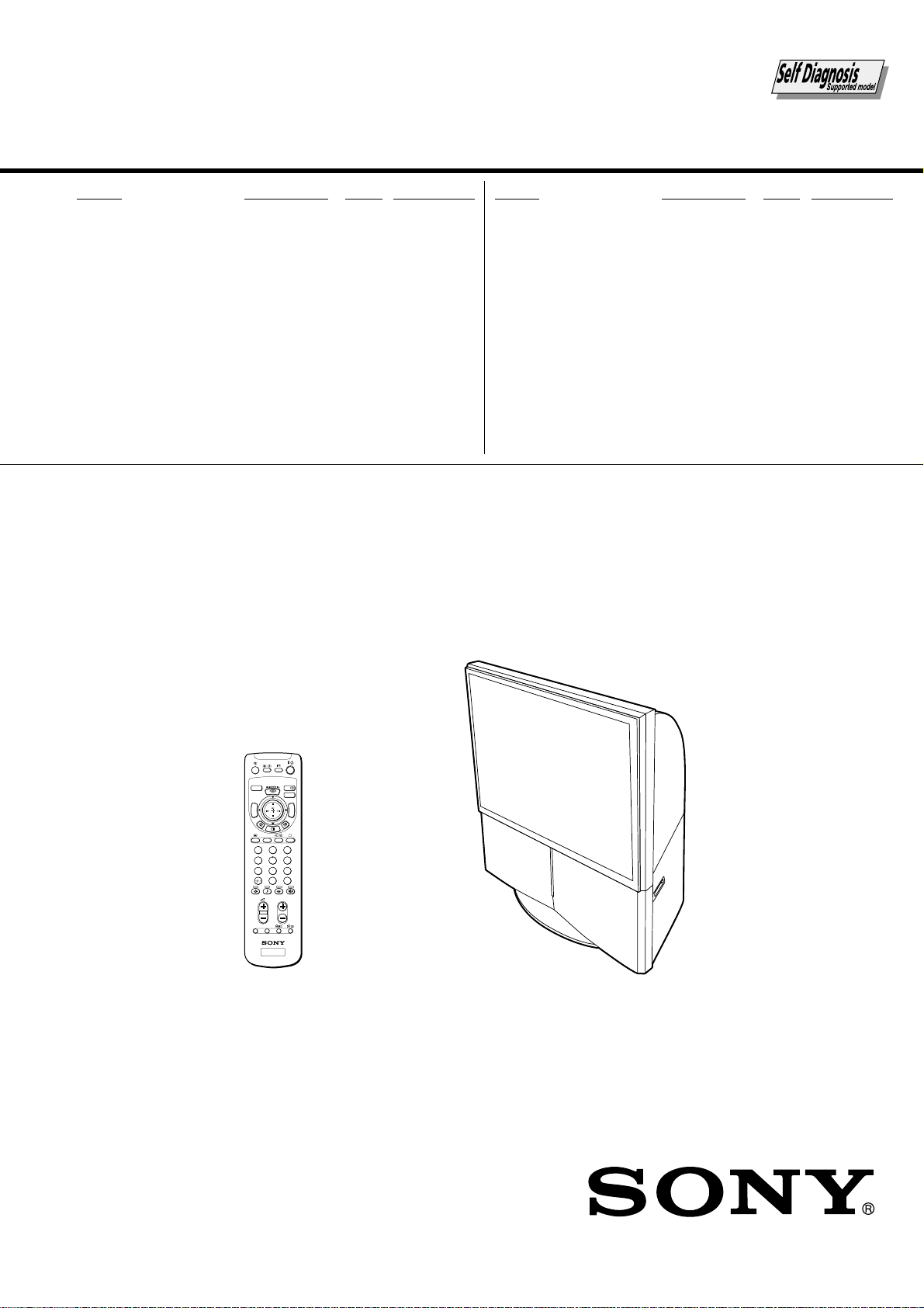
SONY KP-FS57M31, KP-FS57M61, KP-FS57 M90, KP-FS57 M91 Service Manual
SERVICE MANUAL
AG-3X
CHASSIS
MODEL COMMANDER DEST. CHASSIS NO.
KP-FS57M31 RM-997 AUS SCC-XXX-A
KP-FS57M61 RM-997 GE SCC-XXX-A
KP-FS57M90 RM-997 HK SCC-XXX-A
KP-FS57M91 RM-997 ME SCC-XXX-A
MODEL COMMANDER DEST. CHASSIS NO.
VIDEO
A/B
DRC-MF
V CENTER
INDEX
PROG
MENU
HD/DVD
123
456
7809
JUMP
PROG
OPTION RESET
TV
RM-997 KP-FS57M31/M61/M90/M91
PROJECTION TV
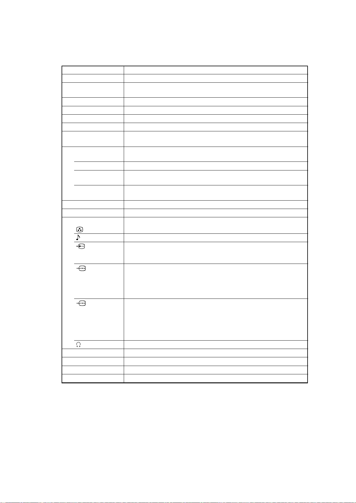
Projection system
Picture tube
Projection lenses
Screen size
Television system
Color system
Stereo/Bilingual
system
Channel coverage
B/G
I
D/K
M
8 (Antenna)
Audio output (Speaker)
Number of terminal
(Video)
(Audio)
(S Video)
(Component
Video)
(G/B/R/HD/
VD Video)
(Headphones)
Power requirements
Power consumption (W)
Dimensions (w/h/d, mm)
Mass (kg)
KP-FS57M31/M61/M90/M91
SPECIFICATIONS
KP-FS57M31/M61/M90/M91
3 picture tubes, 3 lenses, horizontal inline system
7 inch high-brightnes monochorome tubes (6.3 raster size), with optical coupling
and liquid cooling system
High performance, large-diameter highbrid lens F1.0
57 inches
B/G, I, D/K, M
PAL, PAL 60, SECAM, NTSC4.43, NTSC3.58
NICAM Stereo/Bilingual B/G, I;
A2 Stereo/Bilingual (German) B/G
VHF : E2 to E12 / UHF : E21 to E69 / CATV : S01 to
S03, S1 to S41
UHF : B21 to B68 / CATV : S01 to S03, S1 to S41
VHF : C1 to C12, R1 to R12 / UHF : C13 to C57, R21
to R60 / CATV : S01 to S03, S1 to S41, Z1 to Z39
VHF : A2 to A13 / UHF : A14 to A79/
CATV : A-8 to A-2, A to W+4, W+6 to W+84
75-ohm external terminal
15W + 15W (10% distortion)
Input: 4 Output: 1 Phono jacks; 1 Vp-p, 75 ohms
Input: 4 Output: 1 Phono jacks; 500 mVrms
Input: 2 Y: 1 Vp-p, 75 ohms,
unbalanced, sync negative
C: 0.286 Vp-p, 75 ohms
Input: 2 Phono jacks
Y: 1 Vp-p, 75 ohms, sync negative
P
B/CB: 0.7 Vp-p, 75 ohms
P
R/CR: 0.7 Vp-p, 75 ohms
Audio: 500 mVrms
Input: 1 Phono jacks
G: 0.7 Vp-p, 75 ohms
B: 0.7 Vp-p, 75 ohms
R: 0.7 Vp-p, 75 ohms
HD: 0.7 Vp-p, 75 ohms
VD: 0.7 Vp-p, 75 ohms
Output: 1 Stereo minijack
110 - 240 V AC, 50/60Hz
260 W
1360 × 1395 × 688
100
RM-997
Design and specifications are subject to change without notice.
CAUTION
SHORT CIRCUIT THE ANODE OF HTE PICTURE TUBE
AND THE ANODE CAP TO THE METAL CHASSIS, CRT
SHIELD, OR CARBON PAINTED ON THE CRT, AFTER
REMOVING THE ANODE.
SAFETY-RELATED COMPONENT WARNING!!
COMPONENTS IDENTIFIED BY SHADING AND MARK
! ON THE SCHEMATIC DIAGRAMS, EXPLODED
VIEWS AND IN THE PARTS LIST ARE CRITICAL TO
SAFE OPERATION. REPLACE THESE COMPONENTS
WITH SONY PARTS WHOSE PART NUMBERS APPEAR AS SHOWN IN THIS MANUAL OR IN SUPPLEMENTS PUBLISHED BY SONY.
– 2 –

TABLE OF CONTENTS
1. SELF DIAGNOSIS FUNCTION
1-1. Diagnostic Test Indicators ................................. 5
1-2. Display of STANDBY/TIMER
Light Flash Count............................................... 6
1-3. Stopping the STANDBY/TIMER Flash ............ 6
1-4. Self-Diagnostic Screen Display ......................... 7
1-5. Handling of Self-Diagnostic
Screen Display.................................................... 7
1-6. Self-Diagnostic Circuit ...................................... 8
2. DISASSEMBLY
2-1. Rear Board Removal ......................................... 9
2-2. Main Bracket Block Removal ........................... 9
2-3. Service Position ................................................. 9
2-4. Front Panel Removal ......................................... 10
2-5. H1, H2, and H3 Boards Removal ..................... 10
2-6. Beznet and Mirror Cover Removal ................... 11
2-7. Main Bracket Removal ...................................... 11
2-8. G Board Removal ............................................... 12
2-9. Connector Cover Removal ................................. 12
2-10. J Board Removal ................................................ 13
2-11. A1, E, B4, and V2 Boards Removal .................. 13
2-12. A, AD, and D Boards Removal ......................... 14
2-13. Picture Tube Removal ........................................ 14
2-14. High-Voltage and Cable Installation Removal.. 15
2-15. Mechaseal ........................................................... 15
3. SET-UP ADJUSTMENTS
3-1. Screen Voltage Adjustment
(Rough Alignment) ........................................... 16
3-2. Screen (G2) Adjustment .................................... 16
3-3. Focus Rough Adjustment .................................. 16
2-4. Deflection Yoke Tilt Adjustment ...................... 16
3-5. 2-Pole Magnet Adjustment ................................ 17
3-6. Center Magnet Adjustment ................................ 17
3-7. 4-Pole Magnet Adjustment ................................ 17
3-8. Defocus Adjustment ........................................... 17
3-9. Green, Red, and Blue Focus Adjustment
3-9-1. Green, Red, and Blue Lens Focus
Adjustment .................................................... 17
3-9-2. Green, Red, and Blue Electrical Focus
Adjustment .................................................... 17
3-10. Adjustment with Commander ............................ 18
3-10-1. How to Select Each Mode ............................. 18
- 3-10-2. How to Enter Service Mode .......................... 18
3-10-3. Method of Cancellation
from Service Mode ........................................ 19
3-10-4. How to Adjustments ...................................... 19
3-10-5. How to Write the Data ................................... 19
3-10-6. Memory Write Confirmation Method ........... 16
KP-FS57M31/M61/M90/M91
RM-997
Section Title PageSection Title Page
3-11. Service List ......................................................... 20
3-12. Registration Adjustment
3-12-1. Adjustment Flow ............................................ 47
3-12-2. Setup for Adjustment ..................................... 47
3-12-3. Method of Main Deflection Adjustment ....... 47
3-12-4. Operation Method
for Projector Engine (PJE) Mode .................. 48
3-12-5. Method of Projector Engine Adjustment
(Sub Deflection Adjustment)......................... 49
3-13. Auto Convergence Setting ................................. 52
3-14. Blue Offset Adjustment...................................... 52
3-15. White Balance Adjustment ................................ 52
3-16. Auto Convergence Error Code List ................... 53
4. SAFETY RELATED ADJUSTMENT
4-1. HV Regulation Adjustment ............................... 54
4-2. HV Hold-Down Adjustment ............................. 54
4-3. +B Max Voltage Confirmation ......................... 54
4-4. +B OVP Voltage Confirmation ........................ 54
5. ELECTRICAL ADJUSTMENTS
5-1. Picture Quality Adjustment
5-1-1. Preparation ..................................................... 55
5-1-2. NTSC Video Input ......................................... 56
5-1-3. NTSC RF Input .............................................. 56
5-1-4. PAL Video Input ............................................ 57
5-1-5. PAL RF Input ................................................. 57
5-2. Color Offset ........................................................ 57
6. DIAGRAMS
6-1. Block Diagrams .................................................. 58
6-2. Frame Schematic Diagram................................. 78
6-3. Circuit Boards Location ..................................... 80
6-4. Schematic Diagrams........................................... 82
(1)-(3) Schematic Diagram of A Board .................... 82
(4) Schematic Diagram of A1 Board .................. 88
(5)-(8) Schematic Diagram of AD Board.................. 90
(9)-(15) Schematic Diagram of B4 Board ................... 98
(16) Schematic Diagram of CR,CG and CB Boards
........................................................................ 112
(17)-(19)Schematic Diagram of D Board ................... 114
(20) Schematic Diagram of E Board ..................... 120
(21) Schematic Diagram of G Board .................... 122
(22) Schematic Diagram of H1,H2 and H3 Boards
........................................................................ 124
(23)-(27)Schematic Diagram of J Board .................... 126
(28) Schematic Diagram of SR, V2, and VM Boards
........................................................................ 136
(29) Schematic Diagram of HM Boards ..............
........................................................................ 138
(30)-(31)Schematic Diagram of BM1C Boards ........
........................................................................ 140
– 3 –

Section Title Page
6-5. Printed Wiring Boards ....................................... 144
6-6. Wave Forms ....................................................... 168
6-7. IC Block Diagrams ............................................. 172
6-8. Semiconductors .................................................. 178
7. EXPLODED VIEWS
7-1. Front Panel Block ............................................. 181
7-2. Cabinet Block (KP-FS53) ................................ 182
7-3. Cabinet Block (KP-FS43) ................................. 183
7-4. Bezenet and Mirror Cover Block (KP-FS53) ... 184
8. ELECTRICAL PARTS LIST ............................ 185
KP-FS57M31/M61/M90/M91
RM-997
– 4 –
KP-FS57M31/M61/M90/M91
SECTION 1
SELF DIAGNOSIS FUNCTION
The unit in this manual contain a self-diagnostic function. If any error occurs, the STANDBY/TIMER lamp will automatically
begin to flash.
The number of times the lamp flashes translates to a probable source of the problem. A definition of the STANDBY/TIMER
lamp flash indicators is listed in the instruction manual for the user's knowledge and reference. If an error symptom cannot be
reproduced, the remote commander can be used to review the failure occurrence data stored in memory to reveal past problems
and how often these problems occur.
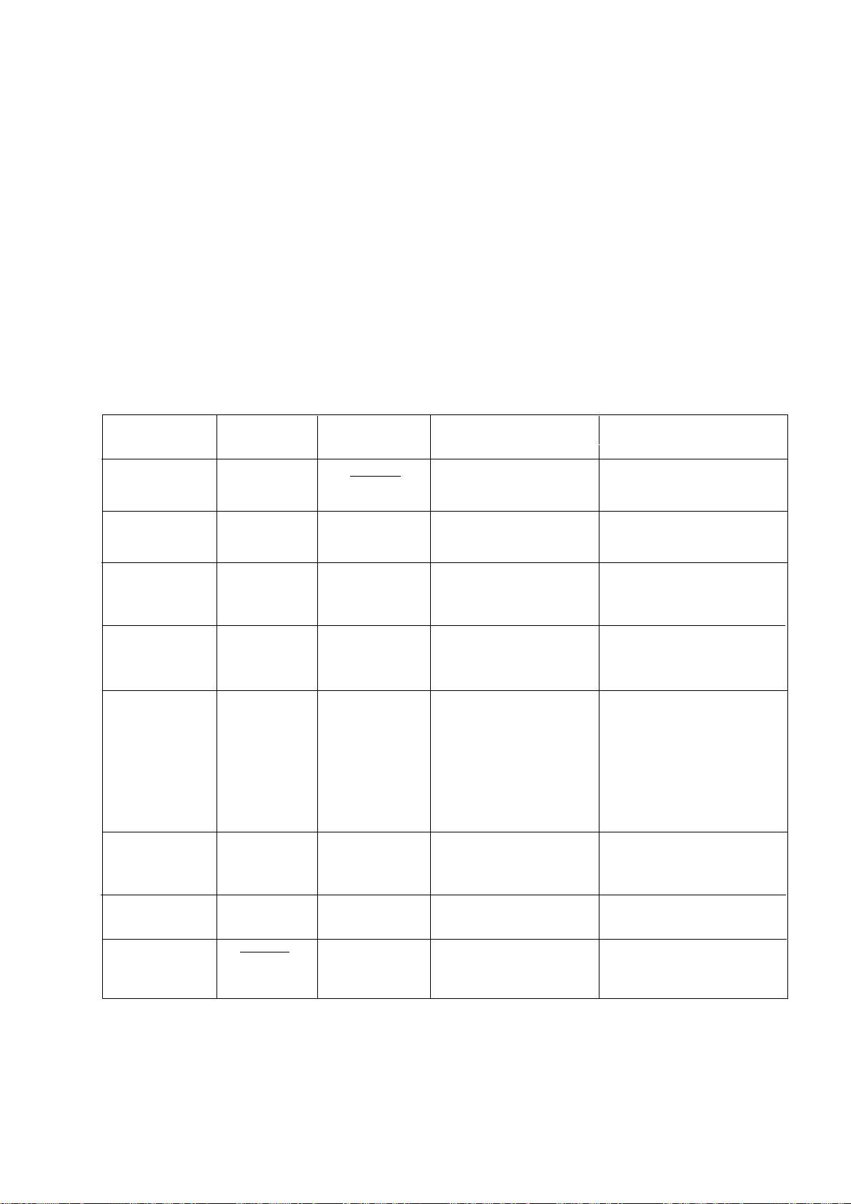
1-1. DIAGNOSTIC TEST INDICATORS
When any error occurs, the STANDBY/TIMER lamp will flash a set number of times to indicate the possible cause of the
problem. If there is more than one error, the lamp will identify the first of the problem areas.
Result for all of the following diagnostic items are displayed on screen. No error has occurred if the screen displays a “0”.
RM-997
Diagnostic
Item
Description
•Power does not
turn on
•+B overcurrent
(OCP)
•+B overvoltage
(OVP)
•Vertical deflection
failure
•White balance
failure
(no PICTURE)
•
Horizontal deflection
failure or +5v down
or High Voltage
failure
No. of times
STANDBY/TIMER
lamp flashes
Does not light
2 times
3 times
4 times
5 times
6 times
Self-diagnostic
display/
Diagnostic result
002:000 or
002:001 ~ 255
003:000 or
003:001 ~ 255
004:000 or
004:001 ~ 255
005:000 or
005:001 ~ 255
006:000 or
006:001 ~ 255
Probable Cause Location
•Power cord is not plugged in.
•Fuse (F6701) is burned out.
(G board)
•H. OUT Q8024 is shorted.
•H. LIN Q8027 is shorted.
(D board)
•HV OUT Q8043 is shorted.
•PH6001 faulty.
•+19V is not supplied.
(G board)
•V. OUT IC8003 faulty.
(D board)
•G2 is improperly adjusted.
(Note 1)
•CRT problem.
•Video OUT IC9101 (CR
board), IC9201 (CG board),
IC9001 (CB board) are faulty.
•IC8306 (J board) and IC4300
(E board) are faulty.
•No connection E board to CR
board.
•IC6502 (G board) faulty.
•HV Circuit failure.
Detected Symptoms
•Power does not come on.
•No power is supplied to the PJ.
•AC power supply is faulty.
•Power does not come on.
•Load on power line is shorted.
•+135V is too high.
•Vertical deflection pulse is
stopped.
•Vertical size is too small.
•Vertical deflection stopped.
•No raster is generated.
•CRT cathode current detection
reference pulse output is small.
•Abnormal High voltage.
•Abnormal H.drive.
•+5v down.
•Audio Protection
•Micro reset
Note 1 : Refer to screen (G2) adjustment in section 3-2 of this manual.
7 times
007:000 or
007:001 ~ 255
101:000 or
101:001 ~ 255
•Power supply fails.
•IC1203,1204 (A board) faulty.
•Discharge CRT
(CR, CG, CB boards)
•Static discharge
•External noise
– 5 –
•There is picture but speaker does
not release sound.
•Power is shut down shortly, after
this return back to normal.
•Detect Micro latch up.
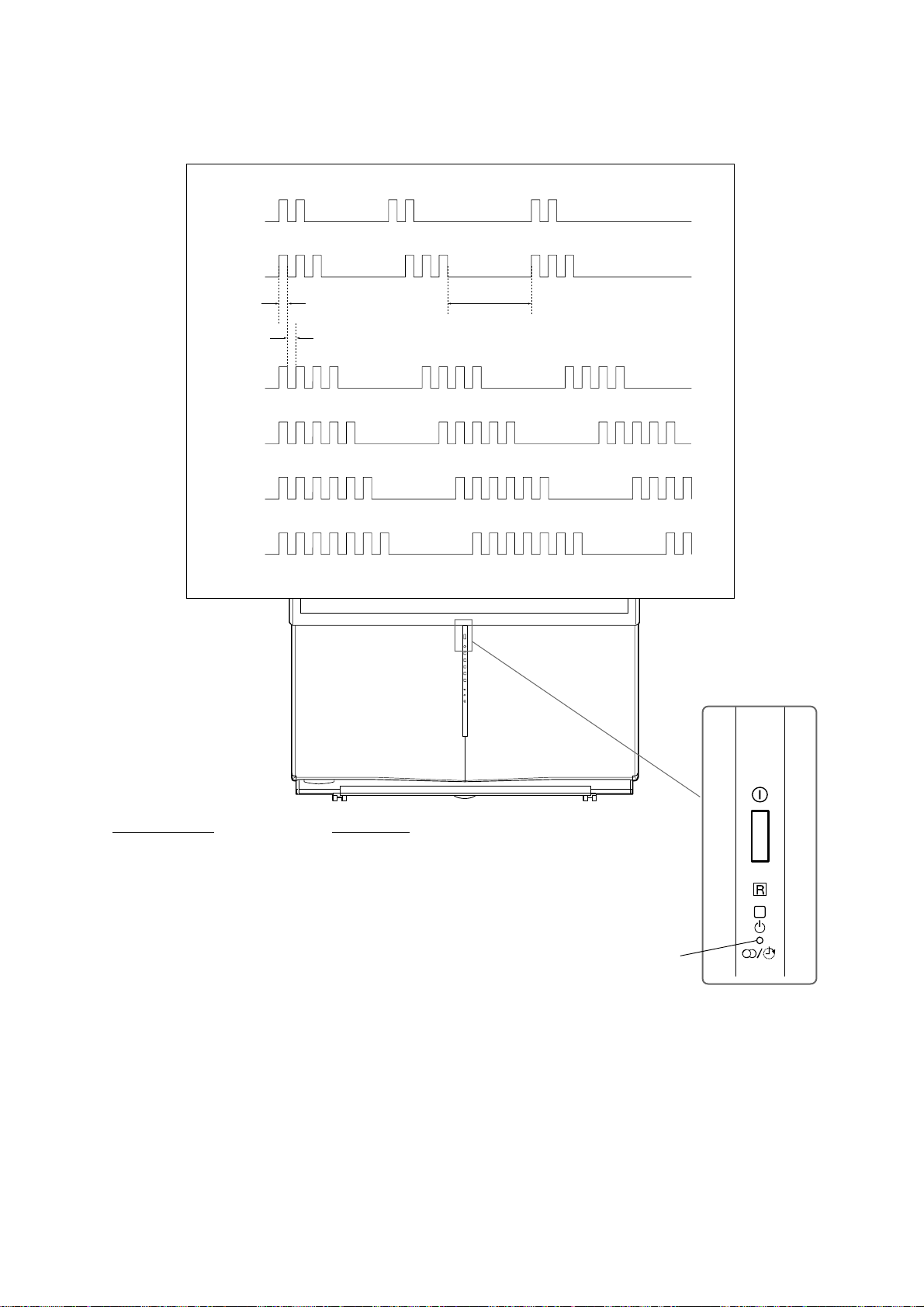
1-2. DISPLAY OF STANDBY/TIMER LIGHT FLASH COUNT
2 times
3 times
Lamp ON
0.3 sec.
Lamp OFF
0.3 sec.
4 times
5 times
Lamp OFF
3 sec.
KP-FS57M31/M61/M90/M91
RM-997
6 times
7 times
Diagnostic Item Flash Count *
+B overcurrent 2 times
+B overvoltage 3 times
V deflection stop 4 times
White balance failure 5 times
High voltage protector 6 times
Audio Protection 7 times
* One flash count is not used for self-diagnostic.
STANDBY/TIMER
lamp
1-3. STOPPING THE STANDBY/TIMER FLASH
Turn off the power switch on the TV main unit or unplug the power cord from the outlet to stop the STANDBY/TIMER lamp from
flashing.
– 6 –
KP-FS57M31/M61/M90/M91
1-4. SELF-DIAGNOSTIC SCREEN DISPLAY
For errors with symptoms such as “power sometimes shuts off” or “screen sometimes goes out” that cannot be confirmed, it is
possible to bring up past occurrences of failure for confirmation on the screen:
[To Bring Up Screen Test]
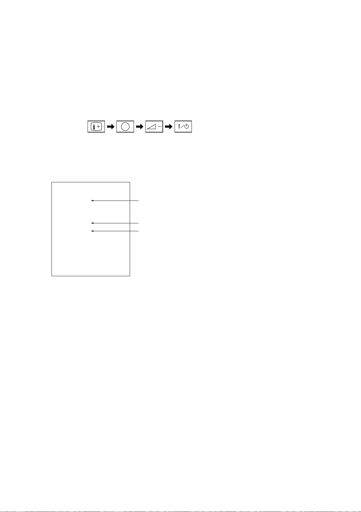
In standby mode, press buttons on the remote commander sequentially in rapid succession as shown below:
Self-Diagnosis screen display
1-5. HANDLING OF SELF-DIAGNOSTIC SCREEN DISPLAY
5
RM-997
(
DISPLAY
Since the diagnostic results displayed on the screen are not automatically cleared, always check the self-diagnostic screen
SELF DIAGNOSTIC
(DIGIT 5) (VOLUME –) (POWER)ON SCREEN
)
002:000
*
* : Note that this differs from entering the service mode (volume +)
Numeral “0” means that no fault has been detected.
003:000
004:000
005:001
006:002
Numeral “1” means a fault has been detected.
Numeral “2” means two faults have been detected.
007:000
101:000
during repairs. When you have completed the repairs, clear the result display to “0”.
Unless the result display is cleared to “0”, the self-diagnostic function will not be able to detect subsequent faults after completion of the repairs.
[Clearing the result display]
To clear the result display to “0”, press button on the remote commander sequentially as shown below when the diagnostic
screen is being displayed.
Press “8” button
(It will indicate “CLEAR” on the screen.)
,
(The “CLEAR” display change to red color.)
Press “-” button
[Quitting Self-diagnostic screen]
To quit the entire self-diagnostic screen, turn off the power switch on the remote commander or the main unit.
– 7 –
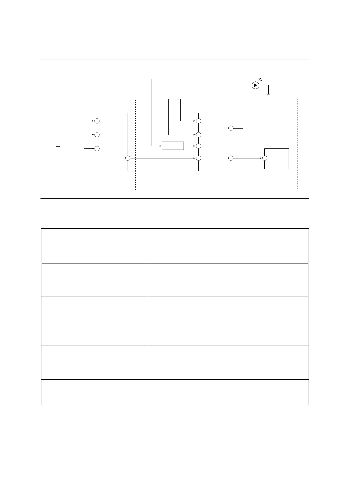
1-6. SELF-DIAGNOSTIC CIRCUIT
IC4300
Y/C JUNGLE
From IC1203,1204
(A board)
From G board
OCP
OVP
KP-FS57M31/M61/M90/M91
RM-997
To H1 board
IC001
SYSTEM
24 IKINFrom CRT (IK)
H
V
(D board)
(D board)
57 XRAYFrom IC8005,8006
56 V PROTFrom Q8001
SDA 52 13 SDA0 SDA1 SDA15 5
Q1209-1211
5 OCP
8 OVP
100
SPPROT
LED1 22
IC003
MEMORY
CXA2170Q CXP961048-003Q
A boardE board
+B overcurrent (OCP) Occurs when an overcurrent on the +B (135 V) line is detected by
Q6504.
Then the voltage to pin 5 of IC001 goes UP. The unit will automatically
turn off.
+B overvoltage (OVP) Occurs when an overvoltage on the +B (135 V) line is detected by
IC6502.
Then the voltage to pin 8 of IC001 goes UP. The unit will automatically
turn off.
Vertical deflection failure Occurs when an absence of the vertical deflection pulse is detected by
Q8001 and D8001. Shut down the power supply.
White balance failure If the RGB levels do not balance or become low level within 5 seconds.
This error will be detected by IC4300.
TV will stay on, but there will be no picture.
High voltage or Horizontal Deflection Protect Occurs when an overvoltage of horizontal pulse is detected by D8038
and IC8006.
If the voltage of pin 1 of IC8006 goes to High, the voltage to pin 57 of
IC4300go to UP. The unit will automatically turn off.
Audio Protector If the Audio out lines become DC.This error will be detected by Q1211,
Q1209 and Q1210.
The unit will automatically turn off.
– 8 –
SECTION 2
DISASSEMBLY
KP-FS57M31/M61/M90/M91
RM-997
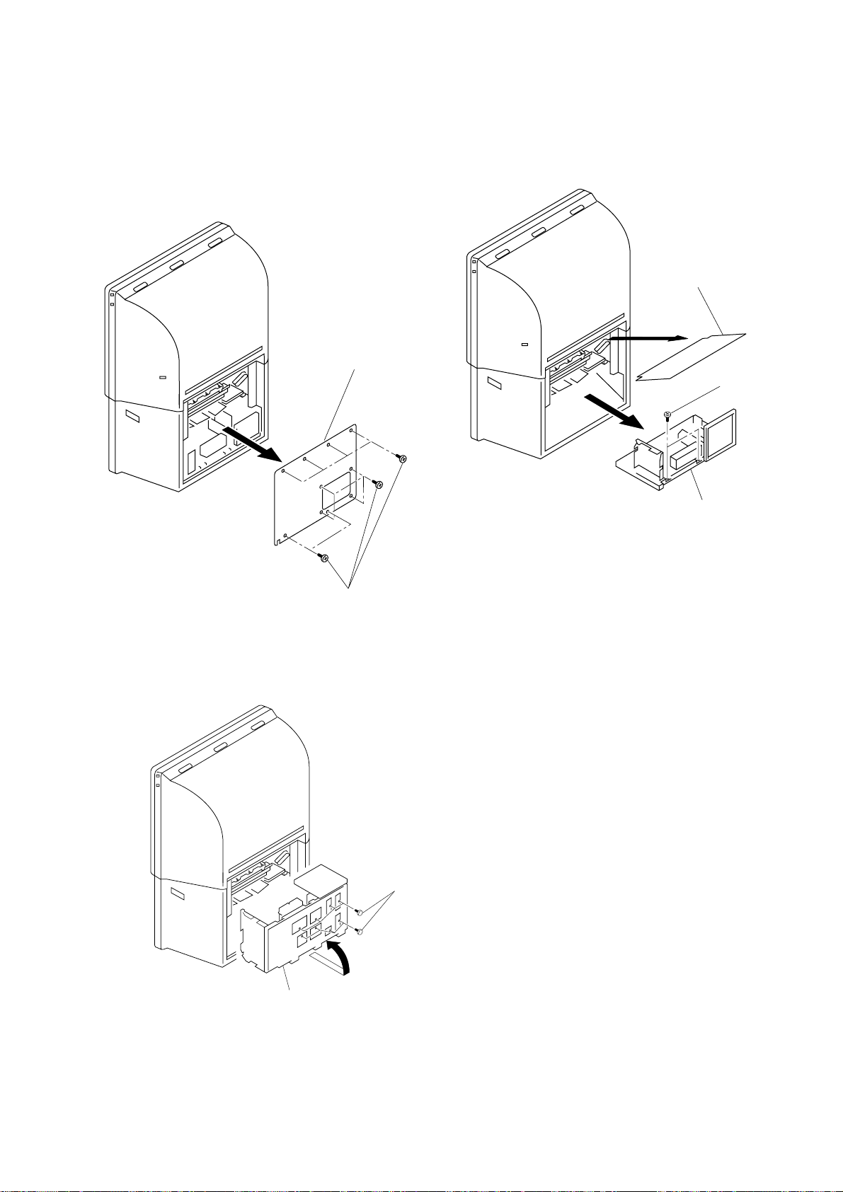
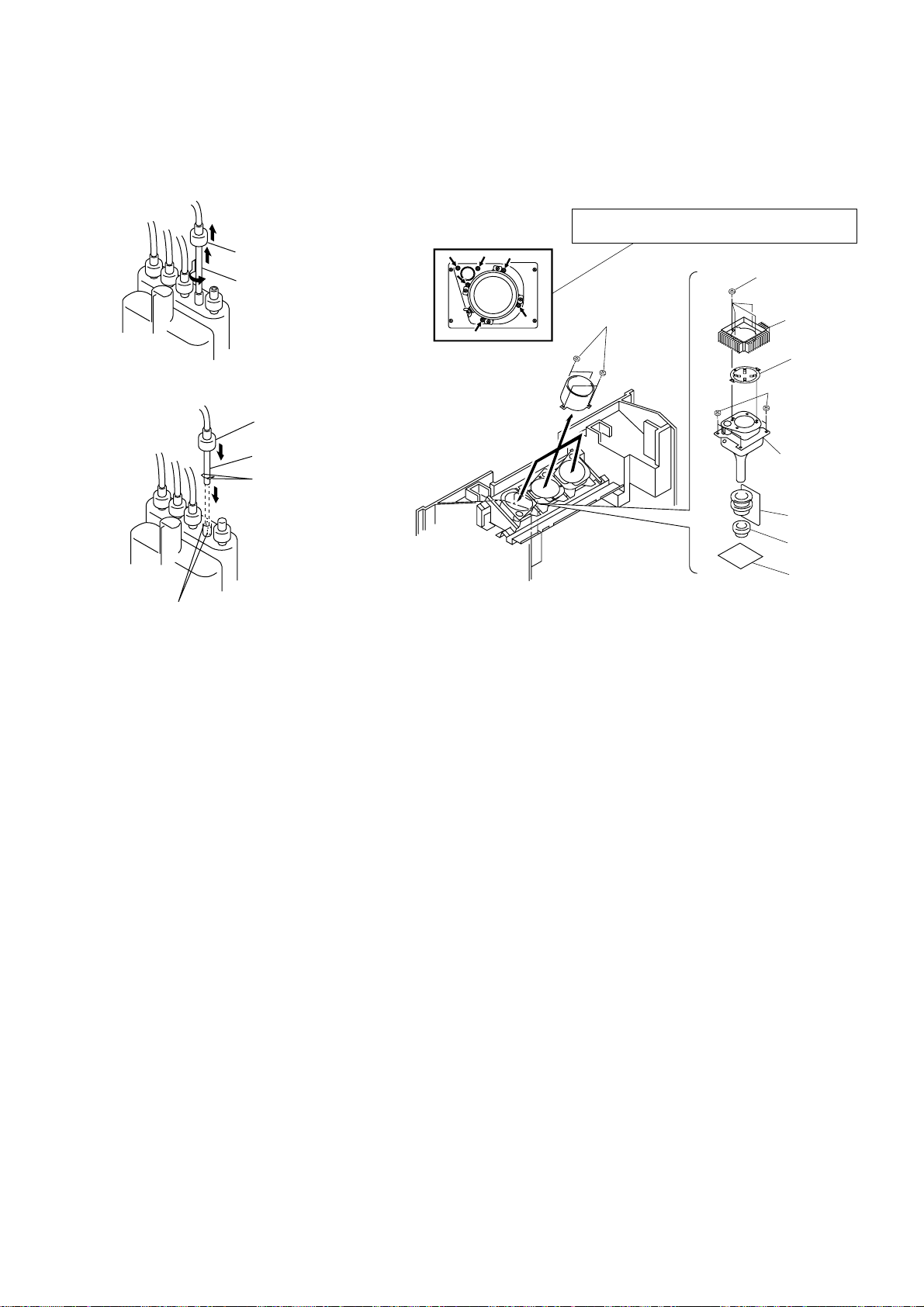
2-1. REAR COVER REMOVAL
2 Rear board
2-2. MAIN BRACKET REMOVAL
1 Optical shield
2 Two screws
(tapping screw
hexagon head)
3 Main bracket section
2-3. SERVICE POSITION
1 Main bracket section
1 Ten screws
(Hexagon head)
2 Eight screws
(BVTP 3X12)
2 COVERS
Cut them off with a plier or the like from
chassis assembly in case of checking
printed circuit boards.
After checking, turn over the covers and
secure them with screws.
(screws 7-685-648-79 -BVTP 3X12)
– 9 –
2-4. FRONT PANEL REMOVAL
2 Two screws
(tapping screw
hexagon head)
KP-FS57M31/M61/M90/M91
RM-997
4 Side panel L(57) assy
3 Two screws
(tapping screw
hexagon head)
1 three screws
(BVTP 4x16)
6 Speaker gril (57)
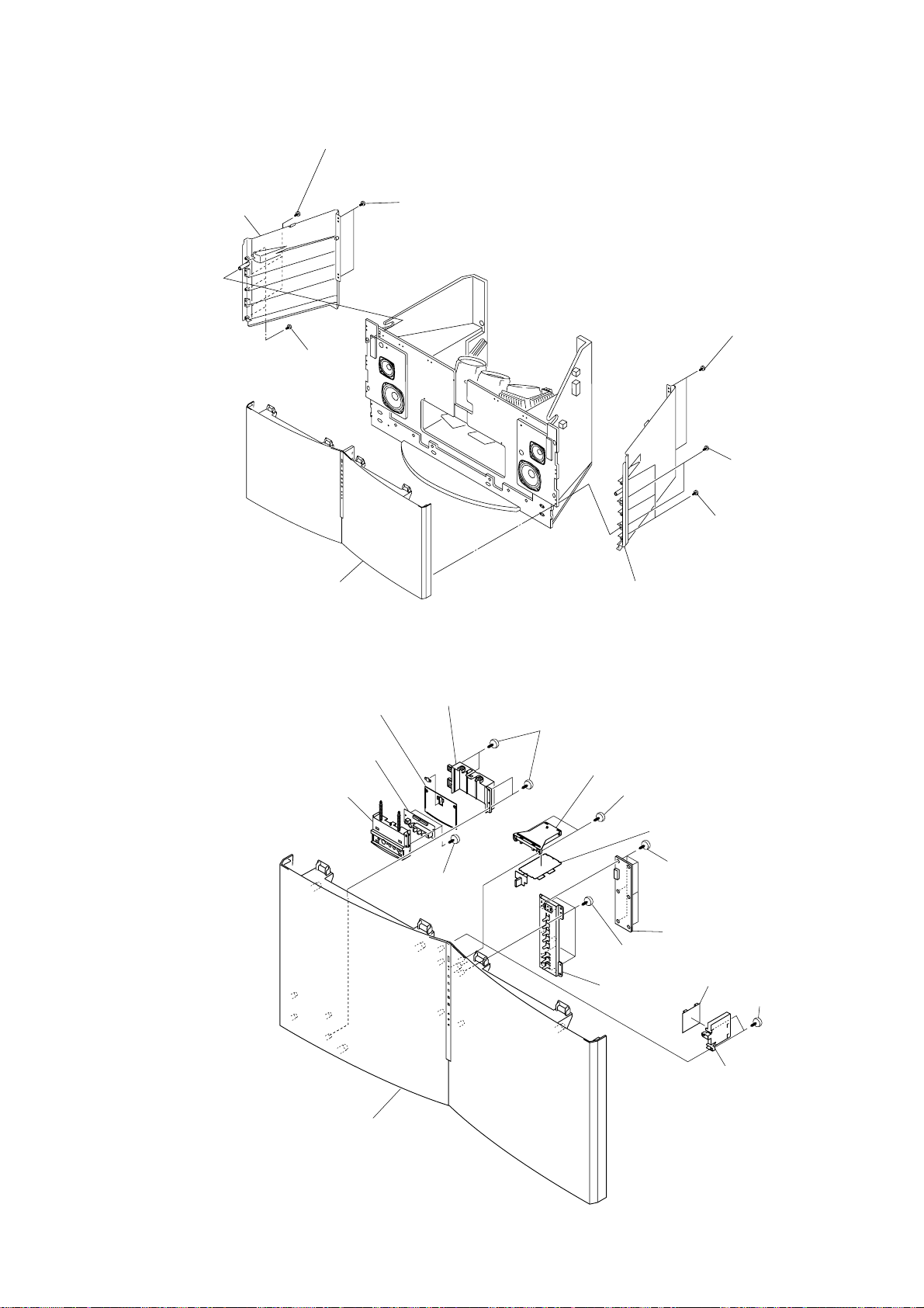
2-5. H1, H2 AND H3 BOARDS REMOVAL
3 Two screws
(tapping screw
hexagon head)
2 Two screws
(tapping screw
hexagon head)
1 three screws
(BVTP 4x16)
5 Side panel R(57) assy
4 Plate input terminal
6 H3 board
3 Cover assy input terminal
Speaker Grill(57) assy
2 Input terminal bracket
5 Two screws
(BVTP 3x12)
1 Four screws
(BVTP 3x12)
8 H1 bracket
qd Control button
7 Two screws
(BVTP 3x12)
9 H1 board
0 Six screws
(BVTP 3x12)
qa H2 board
qs Four screws
(BVTP 3x12)
qh HM board
qf Two screws
(BVTP 3x12)
qg HM bracket
– 10 –
2-6. BEZNET AND MIRROR COVER REMOVAL
7 Ten screws
(BVTP 4X12)
8 Screen
holder
short
6 Screen
qa Diffusion plate (57WF)
qs Diffusion plate (57WL)
holder
8 Screen
holder
short
7 Eleven
holder
short
6 Screen
holder
8 Screen
holder
short
3 Mirror cover
6 Screen
holder
8 Screen
holder
short
6 Screen
holder
7 Seven
holder
short
KP-FS57M31/M61/M90/M91
1 Three screws
(BVTP 4X25)
1 Three screws
(BVTP 4X25)
RM-997
2 Two screws
(Hexagon head)
1 Three screws
(BVTP 4X25)
2 Two screws
(Hexagon head)
2 Four screws
(Hexagon head)
4 Six screws
(Hexagon head)
0 Contrast screen assy
2-7 MAIN BRACKET REMOVAL
1 Two screws
(Tapping screw
hexagon head)
Pay particular attention to the wires
of each printed circuit boards when
puling out the mainbracket.
2 Main bracket section
– 11 –
2-8. G BOARD REMOVAL
KP-FS57M31/M61/M90/M91
RM-997
1 Four holder PWB
2-9. CONNECTOR COVER REMOVAL
2 G board
RF Connector
Main bracket section
3 Connector cover section
2 Screw
(PSW 2.6X6)
Main bracket section
– 12 –
1 Tow screws
(BVTP 4X16)
2-10. J BOARD REMOVAL
KP-FS57M31/M61/M90/M91
RM-997
4 J board
2 J board cover
5 Connector cover
1 Four screws
(BVTP 3X12)
3 Four screws
(BVTP X12)
2-11. A1, E, B4, AND V2 BOARDS REMOVAL
2 E board
1 A1 board
3 Four screws
(Hexagon head)
4 B4 board
5 V2 board
– 13 –
2-12. A, AD AND D BOARDS REMOVAL
KP-FS57M31/M61/M90/M91
RM-997
1 A board
3 Five screws
(BVTP 3X12)
4 D board
2 AD board
2-13. PICTURE TUBE REMOVAL
2 Three screws
(Hexagon head)
(4X20)
4 PICTURE TUBE
BLOCK ASSY
1 Two screws
(BVTP 4X16)
2 Three screws
(Hexagon head)
(4X20)
1 Two screws
(BVTP 4X16)
3 Two screws
(Hexagon head)
(4X20)
5 Two screws
(Hexagon head)
(4X20)
6 Main bracket section
– 14 –
KP-FS57M31/M61/M90/M91
RM-997
2-14 HIGH-VOLTAGE CABLE
INSTALLATION AND REMOVAL
(1) Remover
1 Rubber cap
2 HV cable turn 90°
(2) Installation
2 Rubber cap
1 HV cable
Hook
2-15. MECHASEAL
Removing the arrow-marked screw is strictly inhibited.
If removed, it may cause liquid spill.
1 Four screws
(BVTP 4X16)
7 Two screws
(BVTP 4X16)
8 Heat sink
9 Shade
5 Four screws
(BVTP 4X16)
6 Mechaseal assy
4 Deflection yoke
3 Neck assy
*
Gutter
2 CR board
– 15 –
SECTION 3
SET-UP ADJUSTMENTS
KP-FS57M31/M61/M90/M91
RM-997
3-1. SCREEN VOLTAGE ADJUSTMENT
(ROUGH ALIGNMENT)
1. Receive the Monoscope signal.
2. Set 50% BRIGHTNESS and minimum PICTURE.
3. Turn the red VR on the focus pack all the way to the left and
then gradually turn it to the right until the point where you
can see the retrace line.
4. Next gradually turn it to the left to the position where the
retrace line disappears.
Focus Pack
FOCUS
B
BRG
RG
SCREEN
Fig. 3-1
3-2. SCREEN (G2) ADJUSTMENT
(FINE ADJUSTMENT)
1. Turn on the power of the set.
2. Select VIDEO1 mode without signal.
3. Supply DC 175 ± 0.5 V from external power supply to KR,
KG or KB of CR board, CG board and CB board.(Fig.3-2)
3. Adjust red, green and blue screen voltage to until retrace
line disappears with screen VR on the focus pack.
4. Supply DC 172 ± 0.5 V from external power supply to KR,
KG or KB of CR board, CG board and CB board.(Fig.3-3)
5. Confirm if retrance can be seen.
Power
Supply
+
–
5. Rotate the green lens and align to obtain the best lens focus
at the center area.
6. Rotate the green focus VR on the focus pack and align to
obtain the best electrical focus in the center area.
7. Perform the same alignment for red and blue lenses and electric focus.
8. Fix lens screw.
Scanning line visible.
A
Minimize both A and B.
Lens
Fig. 3-4
B
Fig. 3-5
3-4. DEFLECTION YOKE TILT ADJUSTMENT
1. Receive the Monoscope signal.
2. Place the caps on the red and blue lens so that only the green
color.
3. Loosen the deflection yoke setscrew and align the tilt of the
Deflection yoke so that the bars at the center of the
monoscope pattern are horizontal.
4. After aligning the deflection yoke, fasten it securely to the
funnel-shaped portion of the CRT.
5. The tilt of the deflection yoke for red and blue is aligned the
same as was done for green.
4-pole magnet
2-pole magnet
Deflection yoke
Dummy Resister
3k ohm 20W
Fig. 3-2
3-3. FOCUS ROUGH ADJUSTMENT
1. Loose the lens screw.
2. Set in the service mode.
3. Place the caps on the red and blue lens so that only the green
color is shown.
4. Press “1” or “4” button on the commander and select
“PJE”, press “6” three times on the Commander to display
the test signal (crosshatch) on the screen.
Test signal
Fig. 3-3
– 16 –
Neck Assy
Anode cap
Centering magnet
Make sure deflection yoke is
touching CRT closely.
Fig. 3-6
KP-FS57M31/M61/M90/M91
RM-997
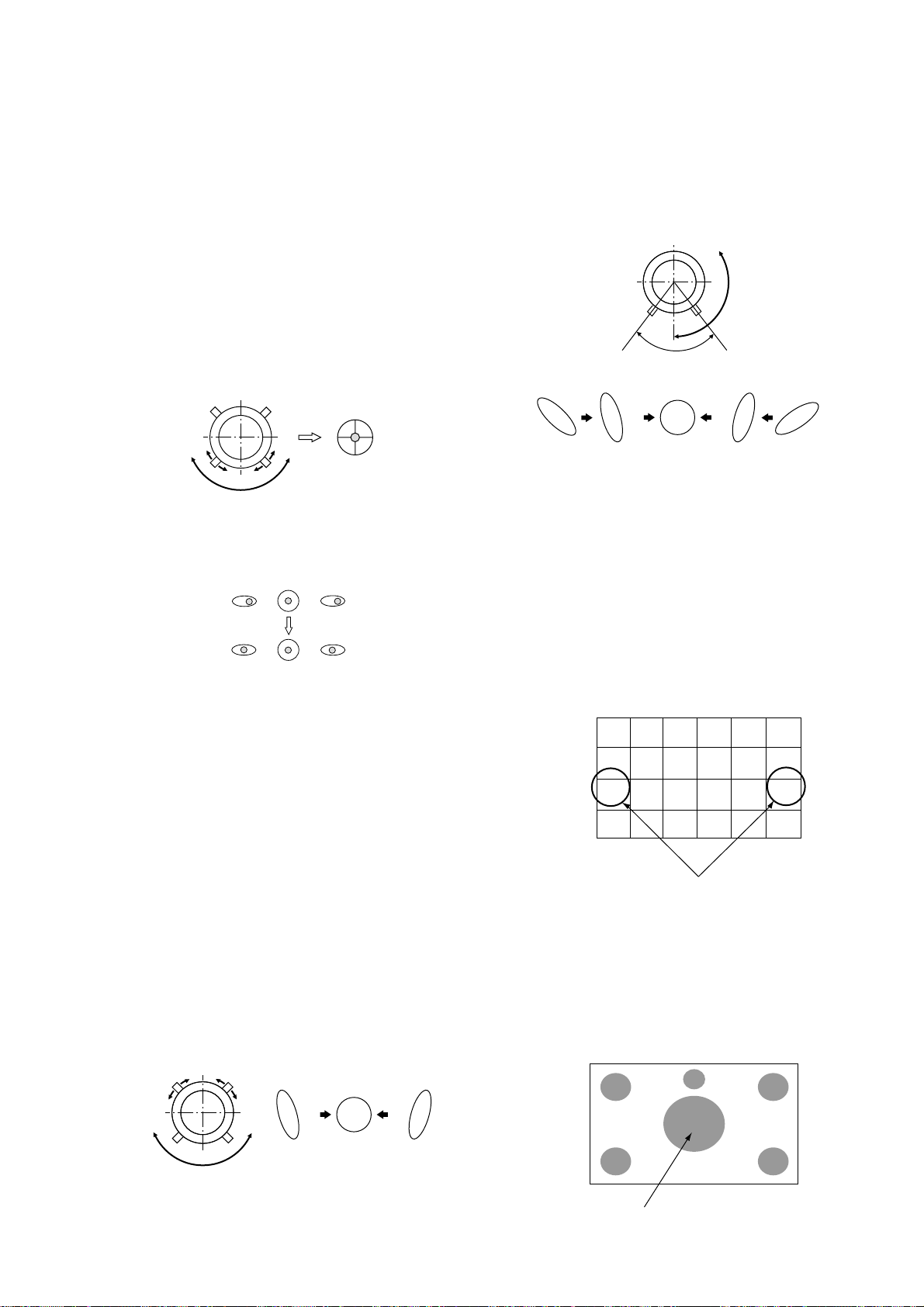
3-5. 2-POLE MAGNET ADJUSTMENT
1. Receive the Dot signal.
2. Place the caps on the red and blue lens so that only the green
color is shown.
3. Turn the green focus VR on the focus pack to the left and set
to under focus to enlarge the spot.
4. Adjust the 2-Pole Magnet so that the bright spot should be
centered.
(center of the dot doesn't move)
5. Align the green focus VR and set for just (precise) focus.
6. Select Dynamic mode, turn BLUE FOCUS VR on the focus
pack to the left.
7. Confirm that right- end and left-end dot core are in center of
dot.
8. If cores are not in center, adjust blue 2 pole magnet as cores
are in center.
Use the center dot
Fig. 3-7
NG
OK
Left-end dot
(BLUE)
Right-end dot
(BLUE)
Fig. 3-8
3-6. CENTERRING MAGNET ADJUSTMENT
1. Receive the SPCB signal.
2. Cover the both red and blue picture lenses with the lens caps
to show only the color.
3. Adjust the green centering magnet to put the center of the
SPCB signal to the center of the screen.
4. Adjust red centering magnet in the same way.
5. Adjust blue centering magnet in the same way.
3-8. DEFOCUS ADJUSTMENT (BLUE)
1. Receive the Dot signal.
2. Cover the both red and green picture lenses with the lens
caps to show only the color..
3. Turn the blue focus VR on the focus pack to the right to
make the round dot elipical.
4. Set 4 pole magnet tab angle 90°.
5. Rotate 4 pole magnet keeping Tab angle 90° make the spot
shape vertical ellipse.
Rotate
90° Fix
OK
Fig. 3-10
3-9. GREEN, RED AND BLUE FOCUS
ADJUSTMENT
3-9-1. Green, Red and Blue Lens Focus Adjustment
1. Receive the Monoscope signal.
2. Place the caps on the red and blue lens so that only the green
color is shown.
3. Rotate the green lens and adjust to obtain the best lens focus
at the center area.
4. Fix lens screw.
5. Repeat above process for red and blue.
6. Rotate the blue lens and adjust to obtain the best lens focus at
the both side area.
7. Fix blue lens screw.
3-7. 4-POLE MAGNET ADJUSTMENT
1. Receive the Dot signal.
2. Place the caps on the red and blue lens so that only the green
color is shown.
3. Turn the green focus VR on the focus pack to the right and
set to over focus to enlarge the spot.
4. Now align the 4-Pole Magnet so that the enlarged spot becomes a perfect circle.
5. Perform the same alignment for red.
Use the center dot
Fig. 3-9
OKNG NG
Adjust Point of Blue
Fig. 3-11
3-9-2. Green and Red Dot/Hatch Electrical Focus
Adjustment
1. Receive the signal.
2. Place the caps on the red and blue lens so that only the green
color is shown.
3. Rotate the green focus VR on the focus pack and adjust to
obtain the best electrical focus in the adjust point.
4. Repeat above process for red and blue.
Adjust Point of Green and Red
Fig. 3-12
– 17 –
KP-FS57M31/M61/M90/M91
Enter the
“Service mode”
5
(DIGIT 5) (VOLUME +)ON SCREEN
DISPLAY
(
)
TV
STANDBY
(
)
RM-997
3-10. ADJUSTMENTS WITH COMMANDER
Service adjustment to this model can performed with the supplied
remote commander RM-998
Copy PAL data
to NTSC
VIDEO
Write data to NVM
blue
Adjustment item
up
Adjustment item
down
User control goes
to the standard state
Read data from
NVM
Change
the PICTUER MODE
DRC-MF
INDEX
PROG
HD/DVD
123
456
7809
PROG
OPTION RESET
TV
RM-997
A/B
V CENTER
MENU
JUMP
Up : Category up
Down : Category down
Push : Enter
Copy data to all
mode
Data up
Data down
Initialize data
(Not stored)
3-10-1. How to Select Each Mode
50 Hz 60 Hz WIDE 60 Hz WIDE 50 Hz
(PAL) (NTSC) (NTSC) (PAL)
DRC1250 aa a a
DRC100 aa a a
TWIN aa
INDEX aa
1. Selection of Mode Between 50 Hz and 60 Hz
50 Hz : Enter the PAL signal.
60 Hz : Enter the NTSC signal.
WIDE 60 Hz : Enter the NTSC signal MENU WIDE ON.
WIDE 50 Hz : Enter the PAL signal MENU WIDE ON.
2. Selection of DRC Mode
1) Press “DRC-MF (blue)” button on the commander, repeatedly until displays the mode that you want to select on the
screen.
→ DRC1250 → DRC100 → PROGRESSIV
Note : The DRC-MF mode is not selectable when using the
“PROGRAM INDEX” or “TWIN” mode is turned “ON”.
3. Selection of WIDE mode
1) Press “MENU” button on the commander and move “
or down to enter the “FEATURE” b “WIDE MODE”.
2) Move “
” up or down to select “ON” or “OFF”, and push
“ (ENTER)” button.
3) Press “MENU” button to return to normal screen.
4. Selection of TWIN mode
1) Press “
2) Press “
(TWIN)” button on the commander.
(TWIN)” button again to return to normal screen.
XX
XX
” up
5. Selection of INDEX mode
1) Press “PROGR INDEX” button on the commander.
2) Press “PROGR INDEX” button again to return to normal
screen.
3-10-2. How to Enter Service Mode
1. Turn on the main power switch to place this set in standby
mode. (LED will light in red.)
2. Press the buttons on the commander as follows, and enter service mode.
3. After entering service mode, reset current aadjustment data.
Then turn off the power switch.
8
(DIGIT 8)
4. Turn on the main power switch and enter mode again as step 2
above.
– 18 –
(ENTER)
Enter the
“Reset”
KP-FS57M31/M61/M90/M91
RM-997
3-10-3. Method of Cancellation from Service
Mode
1. Set the standby mode (Press “ (TV STANDBY)” button on
the commander), then press “
(TV
STANDBY)” button again, hereupon it becomes TV mode.
3-10-4. How to Adjustments
1. Set in the service mode, the following screen will appear.
Category Name Item Name Mode
Item No.
GE1 00 VPS 1C SERVICE 50
0 003Q 2.9M 00 00 01B7
Suffix No.
Software
Version
Data
Total Power On time
(Hours)
2. Press “1” or “4” button on the commander to select the adjustment item.
3. Press “3” or “6” button on the commander to change the
adjustment data.
50 : PAL, SECAM
60 : NTSC
3-10-5. How to Write the Data
1. Set in the service mode.
2. Press “1” or “4” button on the commander, select the adjustment item, and press “3” or “6” button to change the
data.
3. Press “
cate “WRITE” on the screen.
4. Press “-” button on the commander to write into memory.
(The “WRITE” display will be changed to red color while
executing, and back to “SERVICE”.)
Commander Function (Except PJE mode)
Button Mode Description
+ - WRITE Writes data to NVM.
7 + - READ Reads data from NVM.
8 + - NORMAL All user control goes to the standard.
5 + - INITIAL Service data initialization. Not
2 + - COPY Do not operate with a remote
+ - WRT5060
(MUTE)” button on the commander and it will indi-
stored.
(Be sure not to use usually)
commander.
(The data vary with among mode.)
4. Move “
” up or down to select the adjustment category.
When move “ ” up (category up), service mode changes in
the order as shown below.
GE1
GE2
GE3
GE4
WHB
SAJ
* : When it moves from PJE to other categrys,
repeat 1 or 4 button and press it.
DCN
LDG
JGL
YCT
SYC
SYN
AP
MSP
LTI
MD1
MD2
MD3
MD4
MD5
MD6
MD7
3NR
3CM
2CM
TXT
WID
PJE*
OSD
OPM
OPB
Note : Before changing to other modes, press “ (MUTE)” +
“-” buttons on the commander to write the data.
(Omission of this operation causes the data to be returned
to the data before adjustment.)
: Confirm the adjustment mode before writing data for data
values because to vary in each adjustment mode.
: The adjustment item that there are no relations in the ad-
justment is not to change data values because all items are
written in each adjustment mode.
3-10-6. Memory Write Confirmation Method
1. After adjustment, turn off the AC main power switch off.
2. Turn the power switch ON and set in service mode.
3. Call the adjustment items again to confirm adjustments were
made.
– 19 –
3-11. SERVICE LIST
ely in the memory.
mode.
Device Name
(Slave Address)
HD
DRC100
KP-FS57M31/M61/M90/M91
RM-997
CXA2170AQ(86H)
W/Z
W/Z
DRC1250
Zoom
50 Hz
DRC100
Standard Data
Zoom
DRC1250
Full
DRC100
Full
DRC1250
Function
09 09 09
1F 1F 1F 1F 1F 1F
0F 0F 0F 0F 0F 0F
1F 1F 1F 1F 1F 1F
19 19 19 19 19 19
00 00 00 00 00 00
05 05 05 05 05 05
08 08 08 0A 0A 08
1F
19
00
05
08
0F 0F 0F 0F 0F 0F
00 00 00 00 00 00
00 00 00 00 00 00
00 01 01 01 01 00
01 01 01 01 01 01
07 36 33 1C 19 12
1D 1D 1D 1D 1D 1D
00 00 00 04 04 00
1F
0F
0F
00
00
00
01
0A
1D
00
1F 1F 1F 1F 1F 1F
00 00 00 04 04 00
13 13 13 13 13 13
17 17 17 17 17 17
09 09 09
00
1F
13
17
09
1F 1F 1F 1F 1F 1F
00 00 00 00 00 00
00
1F 1F 1F 1F 1F 1F
01 01 01 01 01 01
07 07 07 07 07 07
00 00 00 00 00 00
00 00 00 00 00 00
1F
1F
01
07
00
00
23 1F 23 1F 23 1F
1F 1F 1F 1F 1F 1F
1F 1F 1F 1F 1F 1F
02 02 02 02 02 02
02 02 02 02 02 02
00 00 00 00 00 00
02
02
00
1F 1F 1F 1F 1F 1F
30 30 30 30 30 30
1F
1F
1F
1F
30
VERTICAL SIZE
V SIZE OFF SET (PJ only)
VERTICAL LINEARITY
VERTICAL S CORRECTION
VERTICAL CENTERING
VERTICAL PIN
VERTICAL MIDDLE PIN
HORIZONTAL TRAPEZOID
VERTICAL POSITION
MIDDLE HORIZONTAL TRAPEZOID
Item
01 VSZ
02 VZO
03 VLN
04 VSC
05 VCN
06 VPN
07 MVP
08 HTZ
No. Name
Those are the standard data values written on the microprocessor. Therefore , the data values of the modes and stored respectiv
Note
• Common : The data value of each mode. Other are set up by each mode.
• : Shaded items are fixed data.
• : Though data value is indicated on the screen, it is not used.
• Standard data listed on the Adjustment Item Table are reference valies, therefore it may be different for each model and each
In case of a device replacement, adjustment by rewriting the data value is necessary for some items.
• Note for Different Data :
GE1 00 VPS
Category
09 MHZ
– 20 –
ASPECT SWITCH
ASPECT RATIO
ZOOM SW
VERTICAL SCROLL
0B ASP
0C VSP
0A ZOM
0D VSR
UPPER VERTICAL LINEARITY
LOWER VERTICAL LINEARITY
HORIZONTAL POSITION
HORIZONTAL CENTERING
0E UVL
0F LVL
01 HPS
GE2 00 HCT
HORIZONTAL SIZE
HORIZONTAL S CORRECTION
HORIZONTAL MIDDLE PIN
HORIZONTAL PIN
PIN
02 HSZ
03 SLN
04 MPN
05
PIN OFF SET (PJ only)
UPPER CORNER PIN
LOWER CORNER PIN
UPPER EXTRA CORNER PIN GAIN
UPPER EXTRA CORNER PIN POSITION
LOWER EXTRA CORNER PIN POSITION
LOWER EXTRA CORNER PIN GAIN
06 PN0
07 UCP
08 LCP
09 UXG
0B UXP
0C LXP
0A LXG
PIN PHASE
AFC ANGLE
LINEARITY ANGLE
AFC BOW
EXTRA CORNER PIN POLARITY
0E PPH
0D XPL
LINEARITY BOW
0F VAG
10 LNA
11 VBW
12 LBW
Device NameItem
(Slave Address)
HD
KP-FS57M31/M61/M90/M91
RM-997
CXA2170AQ(86H)
DRC120
ZoomW/Z
ZoomW/Z
DRC1250
Zoom
60 Hz
DRC120
Standard Data
Zoom
DRC1250
Full
DRC1230
Full
DRC1250
1F 1F
1F 1F 1F
1F 1F
No. Name
Category Function
VERTICAL POSITION 19 19 19 19 19 19 19
GE1 00 VPS
HORIZONTAL CENTERING 13 13 13 13 13 13 13
HTZ HORIZONTAL TRAPEZOID 0F 0F 0F 0F 0F 0F 0F
ASP ASPECT SWITCH 01 01 01 01 01 01 000DVSP ASPECT RATIO 05 02 31 2E 18 17 030EVSR VERTICAL SCROLL 1D 1D 1D 1D 1D 1D 1D
MHZ MIDDLE HORIZONTAL TRAPEZOID 00 00 00 00 00 00 000BZOM ZOOM SW 00 00 01 01 01 01 00
01 VSZ VERTICAL SIZE 1F 1F 1F 1F 1F 1F 1F
02 VZO V SIZE OFF SET (PJ only) 00 00 00 00 00 00 00
03 VLN VERTICAL LINEARITY 05 05 05 05 05 05 05
04 VSC VERTICAL S CORRECTION 08 08 08 08 0A 0A 08
05 VCN VERTICAL CENTERING 1F 1F 1F 1F 1F 1F 1F
06 VPN VERTICAL PIN 0F 0F 0F 0F 0F 0F 0F
07 MVP VERTICAL MIDDLE PIN 00 00 00 00 00 00 000809
0A
LVL LOWER VERTICAL LINEARITY 00 00 00 00 00 00 00
UVL UPPER VERTICAL LINEARITY 00 00 00 00 00 00 00
0F
0C
GE2 00 HCT
01 HPS HORIZONTAL POSITION 17 17 17 17 17 17 17
02 HSZ HORIZONTAL SIZE 1F 1F 1F 1F 1F 1F 1F
03 SLN HORIZONTAL S CORRECTION 09 09 09 09 09 09 09
04 MPN HORIZONTAL MIDDLE PIN 00 00 00 00 00 00 00
08 LCP LOWER CORNER PIN 1F 1F 1F 1F 1F 1F 1F
05 PIN HORIZONTAL PIN 01 01 01 01 01 01 01
06 PN0 PIN OFF SET (PJ only) 07 07 07 07 07 07 07
07 UCP UPPER CORNER PIN
09 UXG UPPER EXTRA CORNER PIN GAIN 00 00 00 00 00 00 00
0A LXG LOWER EXTRA CORNER PIN GAIN 00 00 00 00 00 00 00
0E PPH PIN PHASE 1F 23 1F 1F23 1F 23 1F
0B UXP UPPER EXTRA CORNER PIN POSITION 02 02 02 02 02 02 02
0F VAG AFC ANGLE 1F 1F 1F 1F 1F 1F 1F
0C LXP LOWER EXTRA CORNER PIN POSITION 02 02 02 02 02 02 02
0D XPL EXTRA CORNER PIN POLARITY 00 00 00 00 00 00 00
10 LNA LINEARITY ANGLE 1F 1F 1F 1F 1F 1F 1F
11 VBW AFC BOW 1F 1F 1F 1F 1F 1F 1F
12 LBW LINEARITY BOW 30 30 30 30 30 30 30
– 21 –
Device Name
(Slave Address)
HD
W/Z
DRC100
KP-FS57M31/M61/M90/M91
RM-997
CXA2170AQ(86H)
W/Z
DRC1250
Zoom
50 Hz
DRC100
Standard Data
Zoom
DRC1250
Full
DRC100
Full
DRC1250
Function
3F 3F 3F 3F 3F 3F
0F 07 O7 O7 07 0F
01 01 01 01 01 01
01
3F
0F 07 07 07 07 0F
01 00 00 00 01 01
00 00 00 00 00 00
00 00 00 00 00 00
00 00 00 00 00 00
00 00 00 00 00 00
00 00 00 00 00 00
03 03 03 03 03 03
00 00 00 00 00 00
01 01 01 01 01 01
00 00 00 00 00 00
00 00 00 00 00 00
09 09 09 09 09 09
00 00 00 00 00 00
00 00 00 00 00 00
50 50 50 50 50 50
19 19 19 19 19 19
00 00 00 00 00 00
00 00 00 00 00 00
00 00 00 00 00 00
00 00 00 00 00 00
17 17 17 17 17 17
00
00
01
00
00
00
00
00
03
00
01
00
00
16
00
00
50
19
17
00
00 00 00 00 00 00
00
00
00
00
1F 1F 1F 1F 1F 1F
11 11 11 11 11 11
07 07 07 07 07 07
14 14 14 14 14 14
3C 3C 3C 3C 3C 3C
07 07 07 07 07 07
00 00 00 00 00 00
1F
11
3C
07
14
07
00
Item
HORIZONTAL BLANKING SWITCH
No. Name
GE3 00 HBL
Category
BOTTOM BLANKING
BLANKING OFF
TOP BLANKING
LEFT BLANKING
RIGHT BLANKING
VERTICAL BLANKING SWITCH
05 BBL
06 BLK
04 TBL
01 LBL
02 RBL
03 VBL
VERTICAL COMPENSATION
07 VCM
HORIZONTAL COMPENSATION
08 HCM
AFC COMPENSATION
PIN COMPENSATION
AFC LOOP GAIN
REFERENCE PULSE JUMP SWITCH
VERTICAL DRIVE JUMP SWITCH
VERTICAL DRIVE START SWITCH
PIN DC LEVEL SHIFT
AKB TIMING
0E RST
0C JMP
0D VSW
0F EWD
10 AKT
09 ACM
0B AFC
0A PCM
PIN COMP POLARITY
FH=15K @ MS MODE
Fh setting @multi-scan
Reciprocal Fh @mult-scan
VERTICAL MULTI-SCAN MODE
FREERUN INTERLACE SETTING
11 PPL
12 M15
13 HFQ
14 HFX
15 VMP
16 ITL
– 22 –
VERTICAL # OF LINE(L)
VERTICAL # OF LINE(H)
AGC SW for PAL
DF SW
DF Phase
DFH
17 VLL
18 VLH
19 AGC
01
GE4 00 DFS
QP Phase
DQP AMPLITUDE
DQP AMPLITUDE VERTICAL MODULATION
DQP AMPLITUDE TILT
02 QPH
03 QAM
04 QAV
05 QAA
DQP DC LEVEL TILT
DQP DC LEVEL
DQP DC LEVEL VERTICAL MODULATION
DQP AMPLITUDE
08 QPP
06 QPC
07 QPV
09 QAM
DQP AMPLITUDE VERTICAL MODULATION
0A QAV
DQP AMPLITUDE TILT
0B QAA
COPY FUNCTION (Full to Vcomp/normal)
0C CPY
Device NameItem
(Slave Address)
HD
CXA2170AQ(86H)
KP-FS57M31/M61/M90/M91
RM-997
14
3C1700
W/Z
DRC120
W/Z
DRC1250
Zoom
60 Hz
DRC120
Standard Data
Zoom
DRC1250
Full
DRC120
Full
DRC1250
14
14
14
14
14
3C1700
3C1700
3C1700
3C1700
3C1700
No. Name
Category Function
HORIZONTAL BLANKING SWITCH 01 01 01 01 01 01 01
GE3 00 HBL
DF SW
DF Phase
DFH
0E RST VERTICAL DRIVE START SWITCH 00 00 00 00 00 00 00
01 LBL LEFT BLANKING 3F 3F 3F 3F 3F 3F 3F
02 RBL RIGHT BLANKING 17 17 17 17 17 17 17
03 VBL VERTICAL BLANKING SWITCH 01 01 01 00 00 00 00
04 TBL TOP BLANKING 00 0A 07 07 07 07 07
05 BBL BOTTOM BLANKING 00 0E 07 07 07 07 07
06 BLK BLANKING OFF 00 00 00 00 00 00 00
07 VCM VERTICAL COMPENSATION 00 00 00 00 00 00 00
0B AFC AFC LOOP GAIN 03 03 03 03 03 03 03
08 HCM HORIZONTAL COMPENSATION 00 00 00 00 00 00 00
09 ACM AFC COMPENSATION 00 00 00 00 00 00 00
0A PCM PIN COMPENSATION 00 00 00 00 00 00 00
0F EWD PIN DC LEVEL SHIFT 00 00 00 00 00 00 00
0C JMP REFERENCE PULSE JUMP SWITCH 00 00 00 00 00 00 00
0D VSW VERTICAL DRIVE JUMP SWITCH 01 01 01 01 01 01 01
10 AKT AKB TIMING 10 09 09 09 09 09 09
11 PPL PIN COMP POLARITY 00 00 00 00 00 00 00
12 M15 FH=15K @ MS MODE 00 00 00 00 00 00 00
13 HFQ Fh setting @multi-scan 50 50 50 50 50 50 50
14 HFX Reciprocal Fh @mult-scan 19 19 19 19 19 19 19
15 VMP VERTICAL MULTI-SCAN MODE 00 00 00 00 00 00 00
16 ITL FREERUN INTERLACE SETTING 00 00 00 00 00 00 00
17 VLL VERTICAL # OF LINE(L) 00 00 00 00 00 00 00
18 VLH VERTICAL # OF LINE(H) 00 00 00 00 00 00 00
19 AGC AGC SW for PAL 00 00 00 00 00 00 00
01
02 QPH QP Phase
03 QAM DQP AMPLITUDE
04 QAV DQP AMPLITUDE VERTICAL MODULATION
05 QAA DQP AMPLITUDE TILT
06 QPC DQP DC LEVEL 11 11 11 11 11 11 11
07 QPV DQP DC LEVEL VERTICAL MODULATION 1F 1F 1F 1F 1F 1F 1F
GE4 00 DFS
0B QAA DQP AMPLITUDE TILT 17
08 QPP DQP DC LEVEL TILT 07 07 07 07 07 07 07
0C CPY COPY FUNCTION (Full to Vcomp/normal) 00
09 QAM DQP AMPLITUDE 14
0A QAV DQP AMPLITUDE VERTICAL MODULATION 3C
– 23 –
WHB 00 YOS
DC Offset Canceller for Y Signal 07
CXA2170AQ(86H)
01 UOS
DC Offset Canceller for Cb Signal 1F 22 2A 27 21 2A 27 1F
02 VOS
DC Offset Canceller for Cr Signal 1F 25 28 29 25 28 29 1F
03 SBR
Sub Brightness Control 1F
04 RDR
R Drive 1F
05 GDR
G Drive 17
06 BDR
B Drive 1F
07 RCT
R Cutoff 1F
08 GCT
G Cutoff 1B
09 BCT
B Cutoff 1F
0A SBO
Sub Brightness Offset 1F
0B RDO
R Drive Offset 1F
0C GDO
G Drive Offset 1F
0D BDO
B Drive Offset 1F
0E RCO
R Cutoff Offset 1F
0F GCO
G Cutoff Offset 1F
10 BCO
B Cutoff Offset 1F
Device Name
(Slave Address)
MS
RGB
*YUV, RGB : Component Signal
SD-I : 480i, 576i
SD-P : 480P, 576P
HD : 720P, 1080i (50/60 Hz)
KP-FS57M31/M61/M90/M91
RM-997
YUV
Others
NVM
Address
Function
Common SD-I SD-P HD SD-I SD-P HD
No. Name
Item
Category
– 24 –
3F 32 25
No. Name
SAJ
14 CLO
Color Offset
07 07 07 07
16
HUO
Hue Offset
07 07 07 09
17 SHO
Sharpness Offset
0F 0F 0F 0F
1A BRO
Brightness Offset
60
Function
0C 08 03
07 07 07
0F 0F 0B
SD - P HDSD - I
YUV
0C 08 03
07 07 07
0F 0F 0F
SD - P HDSD - I
RGB
05
0B
17
MS
0F 06 03
0F 06 03
06
Standard Data
Dynamic Standard Hi-Fine Personal
OthersWD -NTwin / Index
ECO Mode Picture Mode
KP-FS57M31/M61/M90/M91
RM-997
07 07 00 07
07 03 00 03
07 03 00 03
07 03 00 03
06 03 00 03
01 02 00 02
21 1F 1F
2F 2A 22
22 1F 1D
01 01 00 01
1F 1F 1F
00 00 00 00
0C 0C 09 0C
02 02 00 02
Standard Data
EcoOff EcoOn EcoOff EcoOn EcoOff EcoOn
Index
Twin
60
HD/DVDVIDEO HD/DVDVIDEOTV
50
07 07 07 09 09 09
04 04 04 06 06 06
TV
0F 0F 0F 09 09 09
0D 0D 0D 08 08 08
08 0B 0C 0F 08 0B
*1
*1
*1
*1
07 07
VIDEO VIDEOTVTV
50
03
Common
02
00
00
Function
Item
Category
Picture Control
Brightness Control
01 BRT
No. Name
SAJ 00 PIC
Color Control
Hue Control
Sharpness Control
VM Level
02 COL
03 HUE
04 SHP
05 VML
Color Matrix Specification
Color Matrix Specification
Dynamic Color on/off
White Balance Offset Setting
Color Matrix Specification
06 DYC
07 WBS
08 RYR
Gamma Shape Correction
Color Matrix Specification
09 RYB
0A GYR
0B GYB
0C GMS
Gamma Red
Gamma Green
Gamma Blue
0F GMB
0D GMR
0E GMG
DC Transmission Control
Auto Pedestal Level Control
ABL Mode Control
10 DCT
11 APL
12 ABM
Sharpness Offset
Hue Offset
Color Offset
ABL Current detection Vth Control
Color Step Width to the Change of S/N
14 CLO
13 ABT
17 HUO
15 CLW
16 HUO
– 25 –
Hue Offset
Sharpness Step Width to the Change of S/N
Brightness Offset
APED BLACK SIZE INFLECTED SETTING
COLOR ON/OFF SETTING
18 SHW
1A BRO
1B SHO
1C DPL
19 SHW
SAJ: Standard Data *1
Item
Category
KP-FS57M31/M61/M90/M91
RM-997
0000000000
Standard Data
Data
Range
Function
DC AMP3
VCA9
Item
01 YBU
No. Name Common
VCA10
DC AMP2
02 YBL
03 RAP
0000000000000000000000
00
VCA5
VCA6
DC AMP1
VCA1
VCA2
DC AMP4
NS Correction
EW Correction
Left Cross Correction
04 RUB
05 RLB
06 LAP
07 LUB
08 LLB
09 CAJ
01 EWC
02 LX
00
0000000000000000000000
Right Cross Correction
H Shift Correction
Environmental SW
Temperature SW
NS SW
EW SW
RX
03
04 HST
05 ENS
06 TES
07 NSS
08 EWS
NS Correction Gain
EW Correction Gain
Environmental Correction Gain
NS Correction by Environment
Temp. Corr. DC of Left side
Temp. Corr. DC of Left side
09 NSG
0A EWG
0B ENG
0C ENS
0D TLD
0E TLU
00
Temp.Corr. Gain of Left Upper
Temp. Corr. Gain of Left Lower
Temp. Corr. Gain of Right Upper
Temp. Corr. Gain of Right Lower
DH Mute
0F TLL
10 TRD
11 TRU
12 TRL
13 DHM
Category
DCN 00 SHS
LDG 00 NSC
– 26 –
MS
RGBYUV
Dynamic Standard Hi-Fine Personal
KP-FS57M31/M61/M90/M91
RM-997
02 02 00 02
01 01 00 01
Standard Data
SD-I SD-P HD SD-I SD-P HD
60 Picture Mode
TV VIDEO TV VIDEO
01
Common
Function 50
07 07 07 07 0A 0B 0B 0A 0B 0B 0B
01 01 01 01 01 02 03 01 02 03 03
00 01 00 01 01 01 03 01 01 03 03
03 03 03 03 03 03 03 03 03 03 03
07
00
00
00
01 01 01 01 01 01 01 00 01 01 01 00
08 07 0A 07 07 07 0F 07 07 0F 0F
00 00 00 00 00 00 00 00 00 00 00
02 02 02 02 02 02 02 02 02 02 02
03 03 03 03 03 03 00 03 03 00 00
01
00
03
00
01 01 01 01 01 01 01 01 01 01 01
00
00
03
03
00
00
0C
Item
01 RGB RGB Output Selection
No. Name
JGL 00 PON RGB and AKB Reference Pulse Output On/Off
Category
02 AGG Aging Mode Selection
03 BBT RGB Bottom Limitter Control
04 LML RGB Amplitude Limitter Control
05 SCO Sub Picture Control
06 LEV RGB Level for RGB0507 SYS Signal Band Selection
0B LTI Luminance Transient Improvement
08 SF0 Shar pness f0 setting
09 SF1 High f0 shar pness gain control
0A PRO Pre/Over-Shoot Ratio Control
0E VDL VM OUT Phase Control
0F VCR VM OUT Coring Level Setting
0C LTM LTI Mode Setting
0D CTI Chrominance Transient Improvement
10 VFO VM OUT F0 Setting
11 VLM VM OUT Limiter Level Setting
12 SPH H Sync Delay Timing Setting
13 CLP CLP Pulse Phase Control
14 CLG CLP Pulse Gate Setting
– 27 –
AUTO REGI LRGB_LEV
15 CLS CLP Pulse Start Phase Setting
16 YOS DC_OFFSET RANGE FOR Y SIGNAL SETTING
17 YLT Y AMPLITUDE LIMITER LEVEL SETTING
18 YCS Y SIGNAL GAIN SETTING
1B HBS RGB OUTPUT H BLANKING WHEN AKBOFF=0
19 PHA PHASE ADJ
1A AKO AKB_OFF
1C ARG
YCT 00 TNT
Tint Adjustment for NTSC
1F 1F
01 PNG
02 PNI
03 SCL
04 SCT
05 SF0
Sharpness Center Frequency Changing
02
06 SEQ
07 SHG Sharpness Gain Control
07 06 05 06
07
08 YOL
09 BSP
0A COL
Cb/Cr Output Level Control
1A
0B DCR
0C BF0
0D BFQ
0E FSW
BPF/TQF Switch
01
0F SDT
10 LPF
11 YDL
12 B01
Cb Offset1 Adjustment (main route)
0A
13 RO1
14 CDF
V Count Down Frequency Switch
00
15 CDM
16 AFC AFC Sensitivity Switch
00 00
17 MVM
Macrovision Mask + AFC Mask
00
18 SRY
SECAM R-Y Black Adjustment
07
19 SBY
SECAM B-Y Black Adjustment
01
1A BEL
SECAM BELL/HPF Switching
02
1B BLF
1C SVI
1D SGP
SECAM Gate Position Adjustment
00
1E SID
SECAM Sensitivity Switch
01
1F SIH
SECAM Inhibition Switch
00
20 STP
Y Black Level Setup for PAL plus
00
21 ASW
AUTO SWITCH
01
22 3NR
3D NR Operation on/off
01
23 BW6
3D NR for 60Hz non-bust signal on/off
01
24 WSH
Sharpness Gain Step for noise reduction
00
25 WCO
Cb/Cr Output Level Step for noise reduction
00
DVDVIDEO
Standard Data
1F1F
00 00
07
KP-FS57M31/M61/M90/M91
RM-997
TV
50TV 60TV 50Video 60Video 50DVD 60DVD
othersS-Input3DComb2DCombCommon
07 07 07 07
07 07 07 07
01
00
1F
03
00
00
00
02
06 05 05 03
01
01
07
00
00
00
Item
No. Name
Category Function
Sub Color Control
PAL/NTSC Gate Width
PAL/NTSC Sensitivity SW
Sub Contrast Control
Sharpness Equalizer Characteristic
Y-output Level Control
Black Stretch Start Point Changing
DC Restoration Ratio Adjustment
BPF/TQF F0 Adjustment
BPF/TQF Q Adjustment
SECAM Double Trap Switch
Y/Cb/Cr LPF Switch
Y-DL Time Adjustment
Cr Offset1 Adjustment
– 28 –
V Count Down Judge Switch
BELL f0 Adjustment
SECAM V-ID Switch
KP-FS57M31/M61/M90/M91
Sharpness Equalizer Characteristic
03
Macrovision Mask + AFC Mask
00
SECAM B-Y Black Adjustment
01
TV
Video
RM-997
00
1F
1F
1F 1F
Standard Data
COLOR MODE
SECAM NTSC PAL 50 60 50 60
S-InputCommon DVD
00
00
07 07 07 07
07 07 07 07
05 03 03 03
1F
00
01
02
1F
00
07
02
01
00
01
01
01
07
01
00
00
07
07
00
00
00
02
01
01
00
00
Function
Item
Category
Tint Adjustment for NTSC
No. Name
SYC 00 TNT
Sharpness Center Frequency Changing
Sub Contrast Control
Sub Color Control
PAL/NTSC Sensitivity SW
PAL/NTSC Gate Width
06 SEQ
05 SF0
04 SCT
03 SCL
02 PNI
01 PNG
Cb/Cr Output Level Control
Y-output Level Control
Sharpness Gain Control
08 YOL
07 SHG
DC Restoration Ratio Adjustment
Black Stretch Start Point Changing
0B DCR
09 BSP
0A COL
Y-DL Time Adjustment
1-H Addition Switch
BPF/TQF Q Adjustment
BPF/TQF F0 Adjustment
0C BF0
0D BFQ
Y/Cb/Cr LPF Switch
BPF/TQF Switch
SECAM Double Trap Switch
LPF
0E FSW
0F SDT
11 YDL
10
12 NCM
– 29 –
Cb Offset1 Adjustment (main route)
16 CDM
15 CDF
14 RO1
13 B01
17 AFC
18 MVM
SECAM R-Y Black Adjustment
19 SRY
BELL f0 Adjustment
SECAM BELL/HPF Switching
1B BEL
1C BLF
1A SBY
AFC Sensitivity Switch
V Count Down Judge Switch
V Count Down Frequency Switch
Cr Offset1 Adjustment
Y Black Level Setup for PAL plus
SECAM V-ID Switch
1D SVI
SECAM Inhibition Switch
SECAM Gate Position Adjustment
SECAM Sensitivity Switch
1E SGP
1F SID
21 STP
20 SIH
SUB AUTO SWITCH
22 ASW
KP-FS57M31/M61/M90/M91
RM-997
00 01 03
Standard Data
Function
03 03 01
00 01
01 00
03 00
01
00
00
00
00
00
07
01
Dummy Frequency Select
Item
Category
01 VFR Dummy Sync Freq0102 SL1 Input Signal Type for IN10003 SL2 Input Signal Type for IN20104 FSY Sync Identification Mode
No. Name Common fh15k otherfh DVD HD RGB
SYN 00 MAT Matrix Conversion
05 VTC V sync Separation Time Constant
06 HWD Output Pulse Width
07 HSL Sync Separation Mode
08 HTC H-Sync Separation Time Constant
09 HSW YG Out signal Output
0B MAC Macrovision010C DUM Out dummy sync or signal sync
0A HMA Hsync within V sync
0E GSL Gain Select
0D CLK Clock Select
0F CBG CB Gain
10 CRG CR Gain0711 YG Y Gain0712 HFR
– 30 –
 Loading...