

Sony KDL-40SLxxxx Schematic
Triage and Troubleshooting Guide
BRAVIA
Audio
System
Block Diagram
........................................
4
Section 4 - Troubleshooting
..............................................
5
......................................................
5
TV will not Turn ON (Dead Set)
5
TV Shuts Down and Indicates a Protection Mode
5
2X Blink Pattern (Power Supply Failure)
.....................
5
3X Blink Pattern (D1.8V or D2.5V Failure)
6
4X Blink Pattern
6
5X Blink Pattern
...............................
6
6X Blink Pattern (Backlight Failure)
6
7X Blink Pattern (Temperature Failure)
8X Blink Pattern (Audio Failure)
..................................
7
Video Troubleshooting
8
..........................................
8
Main Video Board (BM5-Board) or LVDS Cable
9
9
-Board) and
Assb.
Effects
9
Audio Troubleshooting
.......................................................
2
0
0
.....................................................................
2
0
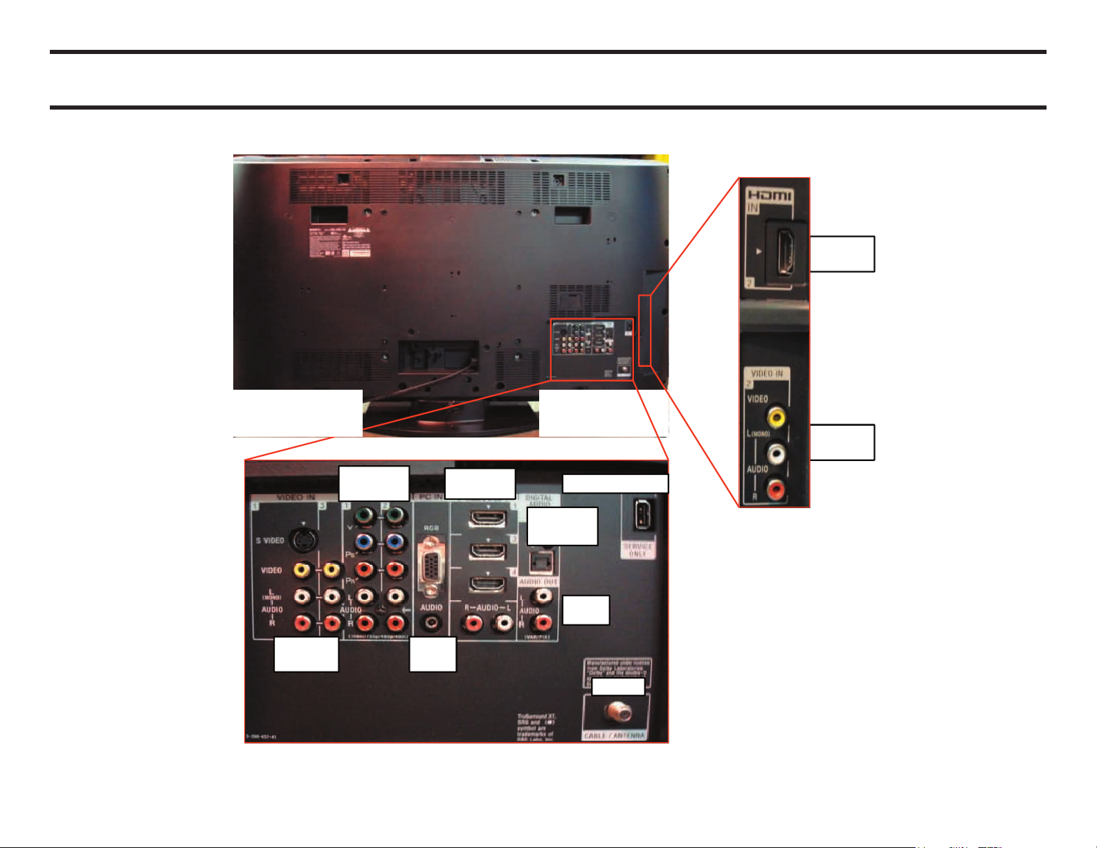
Section 1 - Input & Output Layout and Description
..........
3
Descriptions
............................................................
4
Video & Audio
& 2
..............................
4
& 2
and DVI Audio
"Service Only" USB Connection
..........................................
4
Audio Outputs
..................................................................
4
Analog
Audio Ou
tput (Optical)
Section 2 - Chassis PCB Layout
5
-Board
..........................................................................
7
(Power Supply &
..........................................................................
7
Assembly
8
Section 3 - Block Diagrams
9
9
ystem
Block Diagram
0
tection Circuits
Block Diagram 1
tection Circuits
Block Diagram
Video System
Block Diagram
3
Table of Contents

Table of Contents
TCON Distortions Photographs Fig. 4-4..........................24
TCON Distortions Photographs Fig. 4-5..........................25
Section 5 - Triage Charts & Troubleshooting Flowcharts
2
6
Section 6 - Service Mode & Self Check
...........................
3
6
Composite
Input
HDMI
Input
USB (Service Only)
Composite
Input
Component
Inputs
PC
Inputs
Audio
Output
Digital Audio
Output
(Optical)
HDMI & DVI
Inputs
RF Input
Input & Output Layout and Description
Yellow Jack - Composite Video Input
data stream over the single HDMI connection. In contrast, the DVI format
contains only digital video in its data stream. The audio is sent over a
separate red and white wired analog audio connection. Furthermore, a
The MA2F chassis models (KDL-40SL140 and KDL-46SL140) have a
as a video monitor and audio output (separate Stereo Mini Plug) for the
This USB connection is for Sony factory use only.
Audio Outputs
Analog Fixed Audio Output
This audio output can be used to listen to the TV audio through an external
stereo system. The audio level at the output is set to a fi xed level and
cannot be adjusted.
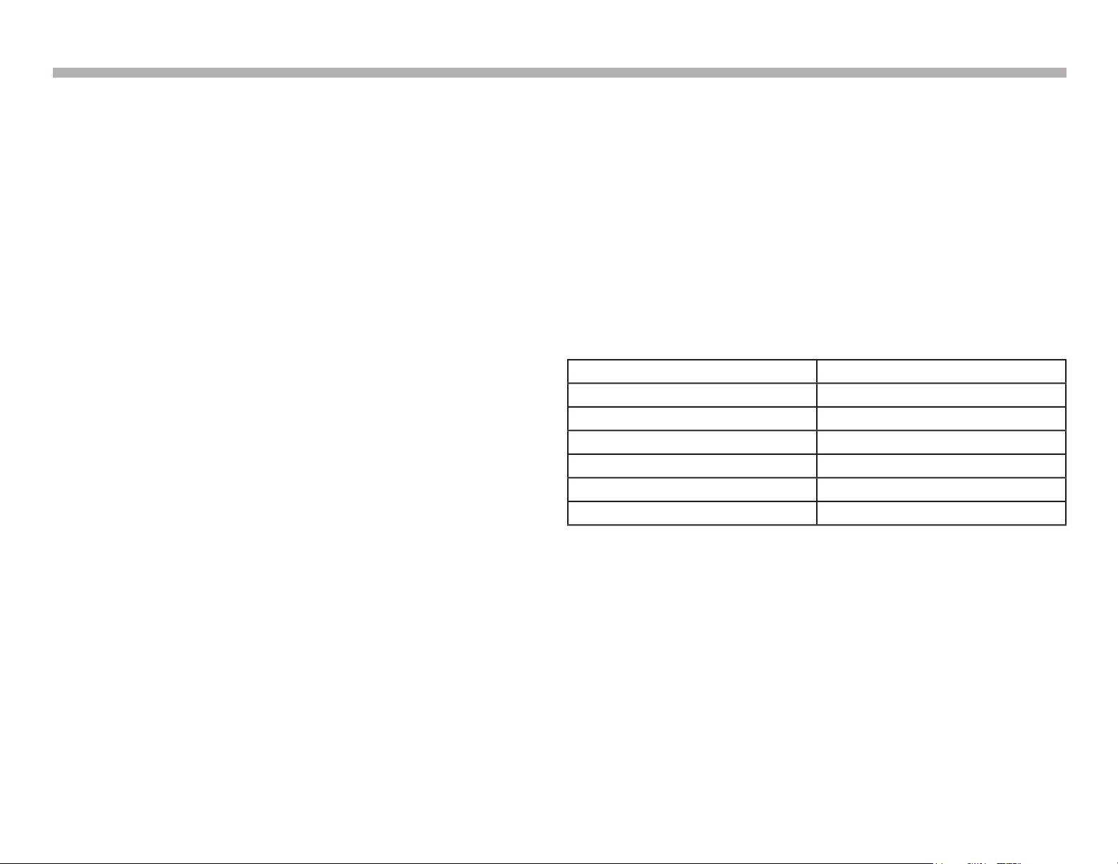
and the audio format which are present at the Optical Audio Output.
Audio Input Source
2CH PCM
2CH PCM
All Analog Audio Inputs
2CH PCM
Analog Tuner (NTSC)
2CH PCM
Balancer
Board
IP5Z -Board
BM5-Board
TCON Board
HM1 -Board
HM5 -Board
KDL-40SL140
LVDS Cable
Balancer
Board
IP5Z -Board
BM5-Board
TCON Board
KDL-46SL140
LVDS Cable
HM1 -Board
H1-Board
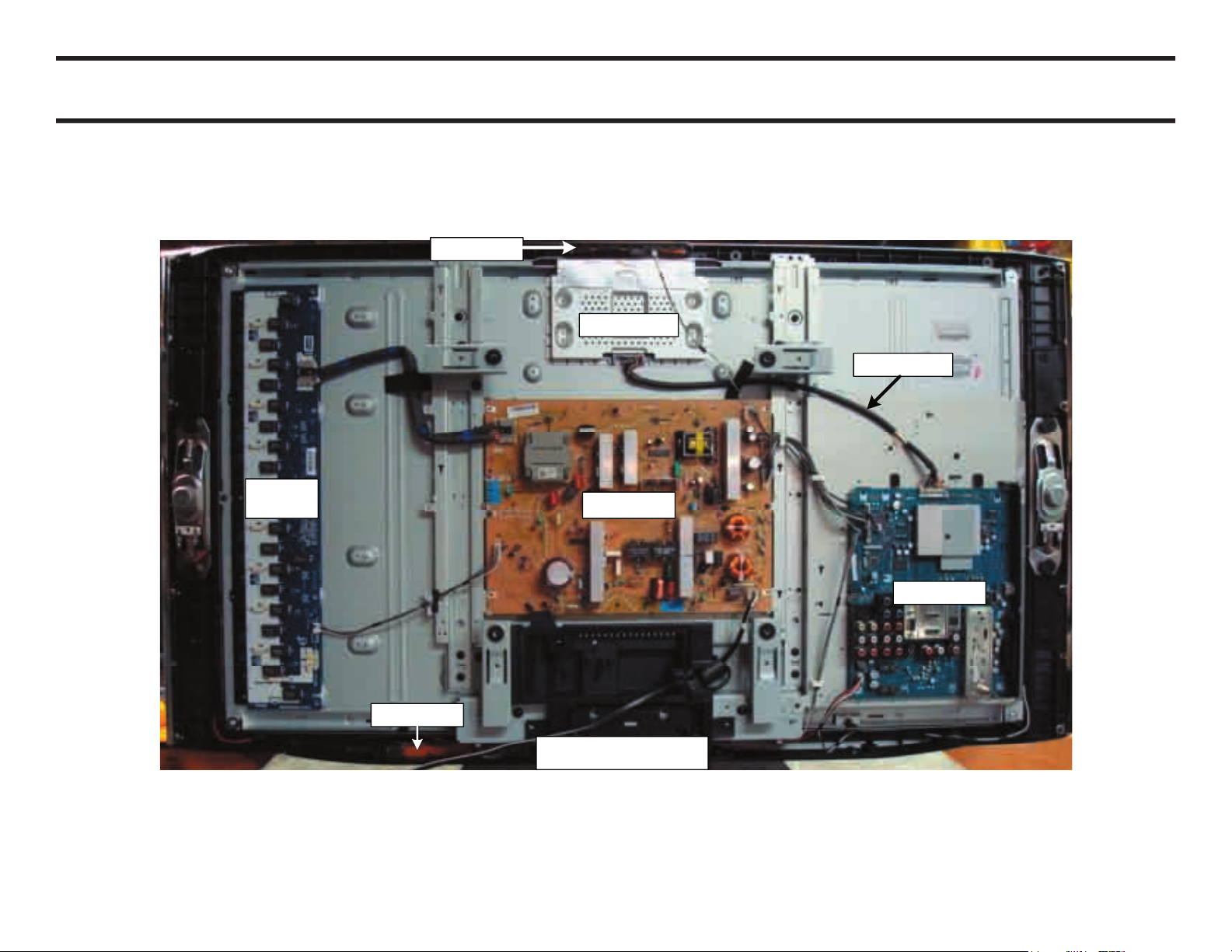
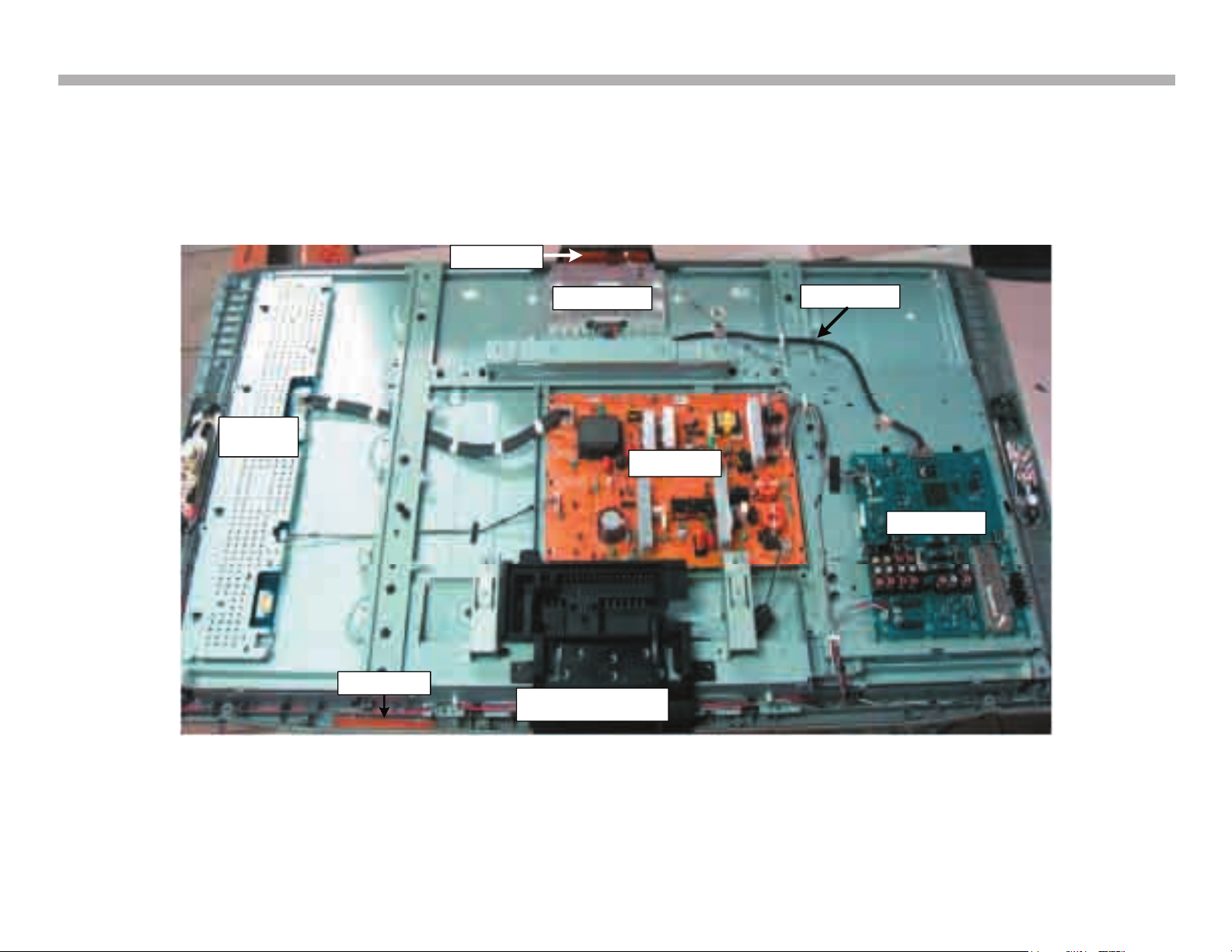
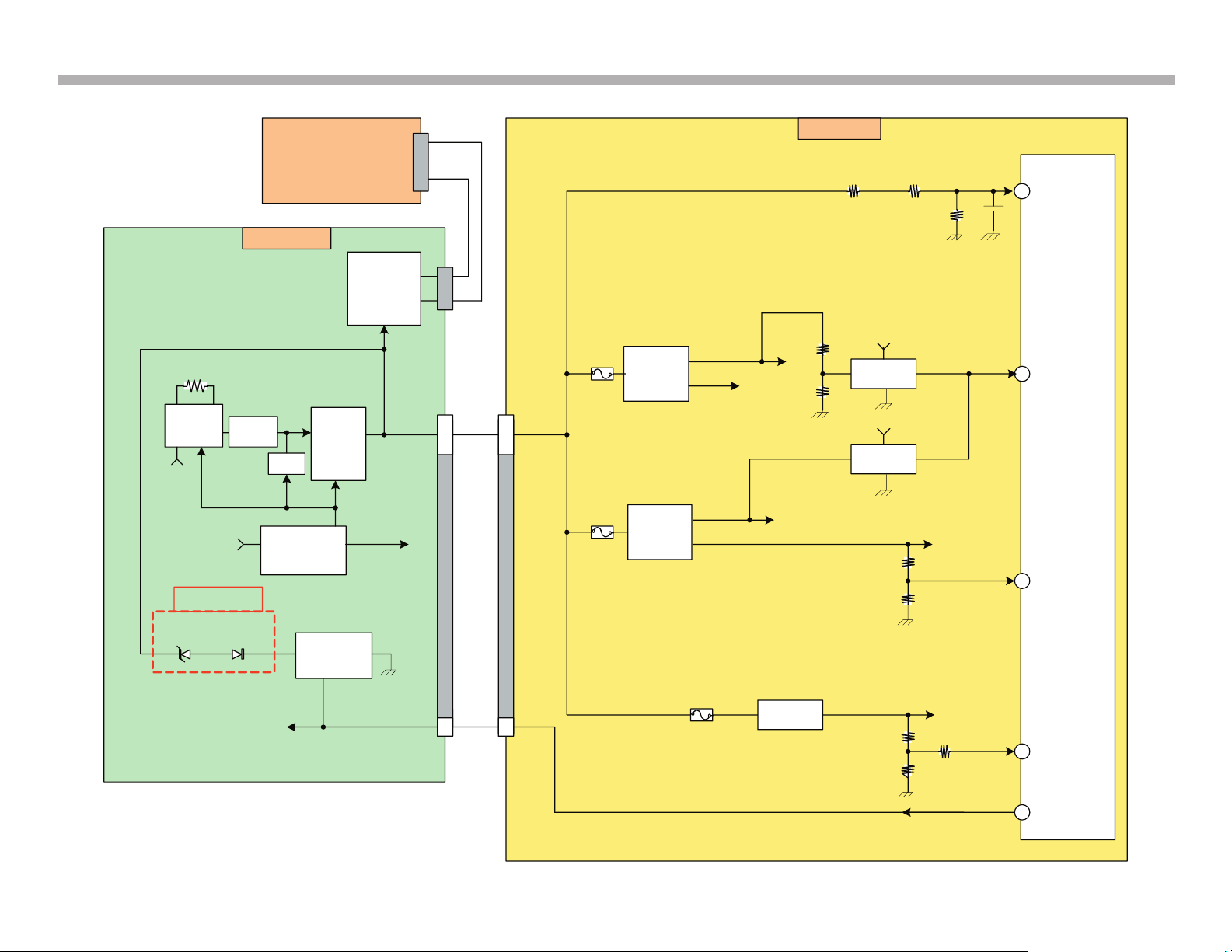
Chassis PCB Layout

Chassis PCB Layout
The circuits located on the BM-Board perform all Video and Audio
circuits. The following circuits are included on this board.
TV Microprocessor
ATSC/NTSC Tuner
Xillion Processor
- A/V Processing
- HDMI Processing
- Scan Converter
Voltage Regulator Circuits
The IP5Z-Board includes the typical TV power supply circuits listed in
the following bullets. In addition this board includes the Backlight Inverter
circuits.
Standby Power Supply
3.3V
AU15V
The Backlight Inverter (or power supply) is located on the IP5Z-Board.
The Backlight Inverter section develops two 1.1KV high voltage outputs
and subsequently the Backlight lamps.
The Backlight Balancer board takes the 1.1KV (HV1 & HV2) from the
equally to each lamp ensuring even luminance across the entire LCD
transformers used for the HV balancing function. In addition, there
are circuits for the Inverter Feedback signal and LD (Lamp Detection)
Volume Up/Down Button
TV/Video Button
Timer/PIC OFF LED

Chassis PCB Layout
The LCD Panel Assembly includes the LCD Panel, TCON, and Backlight
The LCD Panel contains the actual liquid crystals, color fi lters, and
of voltage applied. The panel resolution on all the MA2F chassis models is
The TCON performs all the control, timing, charge, and discharge functions
driving the operation of the LCD Panel.
The Backlight Lamps generate the white light that passes through the
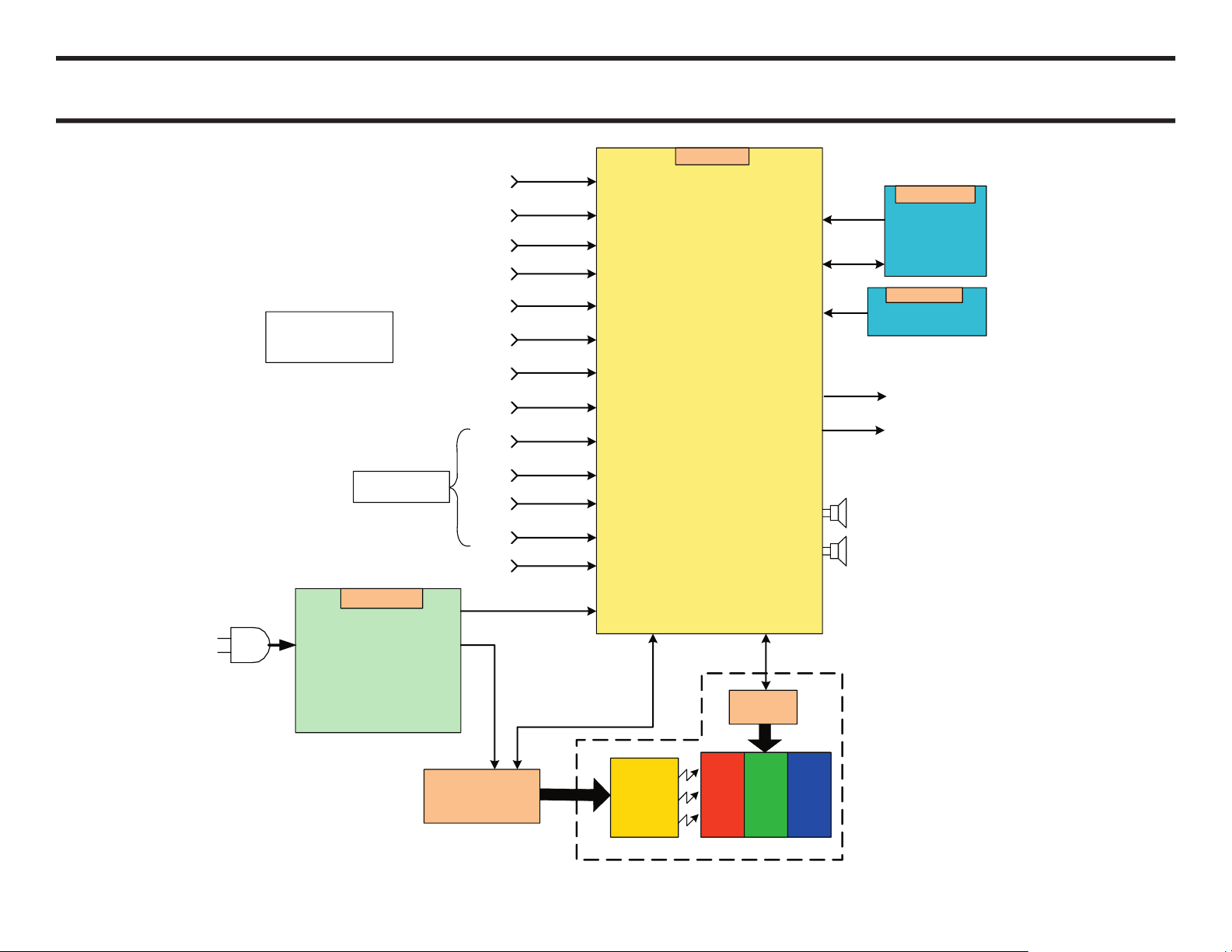
LEDs
IR Sensor
Illumination
Sensor
HM5-Board
Standby 3.3V Power
Supply
Main Power Supply
Inverter HV Supply
Main Relay
IP5Z-Board
AC
Input
Balancer Board
Component 2
R
L
BM5 Board
TV Microprocessor
ATSC/NTSC Tuner
Xillion – A/V Processor
ATSC/NTSC Processing
HDMI
IP (Image Processor)
Scan Converter (Scalar)
Audio Processing
AV Switching
Temperature Sensor
Control Data
Power
LVDS Cable
Power
Keys
SIRCS
Power &
LED Control
TCON
LCD Pane l Assemble
Composite & S-Video 1
LCD PANEL
PC-IN
V
Digital
VAR/FIX Audio O utput
PC-IN Audio Input
Component 1
A/V &
S-Switch
Po wer Switch
Function Keys
HM1-Board
Optical Audio Output
HDMI 1
DVI Audio Input
RF/Cable
HDMI 2
A/V
Analog
A/V
Digital
A/V
Digital
A/V
Analog
A
Analog
A
Analog
CCFT
Backlights
A
Analog
A
Digital
A/V – Audio & Video
A – Audio Only
V – Video Only
Video Only for
DVI connection
RF
Composite Video 2
A/V
Analog
Composite Video 3
A/V
Analog
HDMI 3
HDMI 4
A/V
Digital
A/V
Digital
Block Diagrams
BM5-Board
AU15V
12V
IC7004
Switching
Regulator
3.3V
F7001
F7002
F6001
AC Input
D6000
RY6000
R6009
(6.8ohm)
Resistor/Fuse
CN6700
STBY 3.3V
IC6500
PFC
L800
16.7V
D800
Power ON
(Power 1)
Panel 12V
IC6200
Standby
3.3V
Power
Supply
Power 2
Power 3
CN6000
Switch
Circuit
IC6100
Main
Power
Supply
Balancer Board
LCD
PANEL
IC3011
TV
Micro
STBY 3.3V
CCFL
Backlights
TCON
LCD P anel
Assembly
VC1
VCC
VSense
PH6300
CN4001
1
CN6150
3
Q6100
Q6101
Q6551
IC7005
Switching
Regulator
F4001
IC7007
5V Reg
IC2005
9V Reg
47
/
51
D3.3V
D1.8V
D2.5V
D1.1V
Power 3
5V
9V
Audio
Output
Amp
CN9102
LVDS Cable
11
\
13
4
&
5
4
&
5
11
\
13
1
3
F2000
IP5Z-Board
PH6302
2 2
AC-OFF DE T
To IC3011
3.3V
R6500
(0.47ohm)
Resistor/Fuse
R6200 (10ohm)
Resistor/Fuse
Q6706
Q6707
IC6701
T6600
T6800
12V
IC6702
DRV1
DRV2
Q6602
Q6603
To
Inverter
IC7001
9VReg
9V
Power 2
HV1 – 1.1KV
HV2 – 1.1KV
Power 2
Power 2
1.1KV
(~2KV Strike Voltage)
R6336
16.7V
Q4018
12V Reg
F7000
HM5-Board
IC320
Illumination
Sensor
IC401
IR Sensor
8
CN301
383
CN3008
Block Diagrams
BM5-Board
DC_Alert 1
D3.3V LVP
IC6100
Main
Power
Supply
PFC
DC_Alert 2
D2.5V LVP
D1.8V LVP
DC_Alert 3
Panel V LVP
F4001
Power-ON
3.1V
3.1V
3.3V
12V
3X
5X
IC3011
TV
Micro
4X
IC6200
Standby 3.3V
Power Supply
RY6000
Inrush
Relay
D6000
To Switching Circuit to power
ON IC6100, RY6000, & PFC
AC
Input
STBY
3.3V
CN602
F7002
2X
Reg 5V
3.1V
Power 1
CN4001
11
28
7
16.7V
47
DC_Detect
12V LVP
R6009
IC7005
Switching
Regulator
D1.0V
R4063
R4064
Reg 5V
R4008
R4013
D3.3V
48
R4042
R4043
Panel V (12V)
Q4018
D2.5V
3.1V
R3031 R3034
R3037
F7001
IC7004
Switching
Regulator
R4067
C3007
AC
Input
11
\
13
1
11
\
13
3
Q4001
Q4017
D1.8V
IP5Z-Board
Latch
Q6402
Q6403
D6400
15V
D6401
Backlight
Inverter
Section
Balancer Board
HV1
HV2
CN6700
12V OVP 6X
 Loading...