Sony KDL-40S4100, KDL-46S4100, KDL-52S4100 Training Manual
Training Manual
FX Chassis
Models:
KDL-40S4100
KDL-46S4100
KDL-52S4100
Triage and Troubleshooting Guide
Course: CTV-49
Table of Contents
Section 1 - Input & Output Layout and Description .......... 3
Input Descriptions ............................................................ 4
RF Input ............................................................................... 4
Composite Video & Audio Inputs 1 & 2 ................................ 4
Component Video & Audio
HDMI/DVI Video Inputs 1, 2, & 3 and DVI Audio ................. 4
PC Video & Audio Input ....................................................... 4
"Service Only" USB Connection .......................................... 4
Inputs 1 & 2 .............................. 4
Audio Outputs .................................................................. 4
Analog Fixed Audio Output .................................................. 4
Digital Audio Output (Optical) .............................................. 4
Section 2 - Chassis Layout ................................................. 5
PCB and Component Descriptions .................................. 7
Section 3 - Block Diagrams ................................................ 9
Overall Chassis Block Diagram ....................................... 9
Power System Block Diagram ....................................... 10
Protection Circuits Block Diagram ..................................11
Video System Block Diagram ........................................ 12
Audio System Block Diagram ........................................ 13
TV will not Turn ON (Dead Set) ................................... 14
TV Shuts OFF (No Blink Pattern) ................................ 15
5X Blink Pattern (Lose of 6.5V) ................................... 15
Panel Backlight System ..................................................... 15
Normal Operation ........................................................ 15
Momentary Backlight - 2X Blink Pattern ...................... 15
No Backlight - No Blink Pattern (No Video or Audio) ... 16
There are two failures that will cause this symptom. ... 16
No Backlight - No Blink Pattern (Video & Audio OK) ... 16
There are two failures that will cause this symptom. ... 16
Momentary Backlight - No Blink Pattern
(Video & Audio OK) ...................................................... 17
Backlight ON - No Video -Bright Raster Only
- Audio OK .................................................................. 17
Backlight ON - No Video - Vertical Colored Lines Dis-
played - Audio OK .................................................. 17
Video Processing System ................................................. 17
No Video ...................................................................... 18
Distorted Video ............................................................ 18
The A-Board Affects ..................................................... 18
LCD Panel Assembly Affects (& TCON Board) ............ 19
Section 4 - Troubleshooting ..............................................
Introduction .................................................................... 14
Symptom & Solution ...................................................... 14
Power Supply System ........................................................ 14
Normal Operation ........................................................ 14
14
Section 5 - Technical Troubleshooting Flowcharts ........ 30
Audio Troubleshooting ....................................................... 20
Missing or Distorted Main Speaker Audio - All Inputs .. 20
Missing or Distorted Audio - Individual Inputs .............. 20
Section 6 - Service Mode & Factory Reset ...................... 40
CTV-49 i

Service Mode Item Descriptions .................................... 41
Figures
G-Board Test Points Figure 3-1..........................21
A-Board Test Points Figure 3-2..........................22
Balancer Board Test Points Figure 3-3.................23
LVDS Cable Video Test Points Figure 3-4..........24
A-Board Distortion Photographs Figure 3-5...........25
A-Board Distortion Photographs Figure 3-6........26
TCON Distortion Photographs Figure 3-7...........27
Table of Contents
TCON Distortion Photographs Figure 3-8...........28
HV Connector Removal Figure 3-9........29
CTV-49 ii
Section 1 - Input & Output Layout and Description
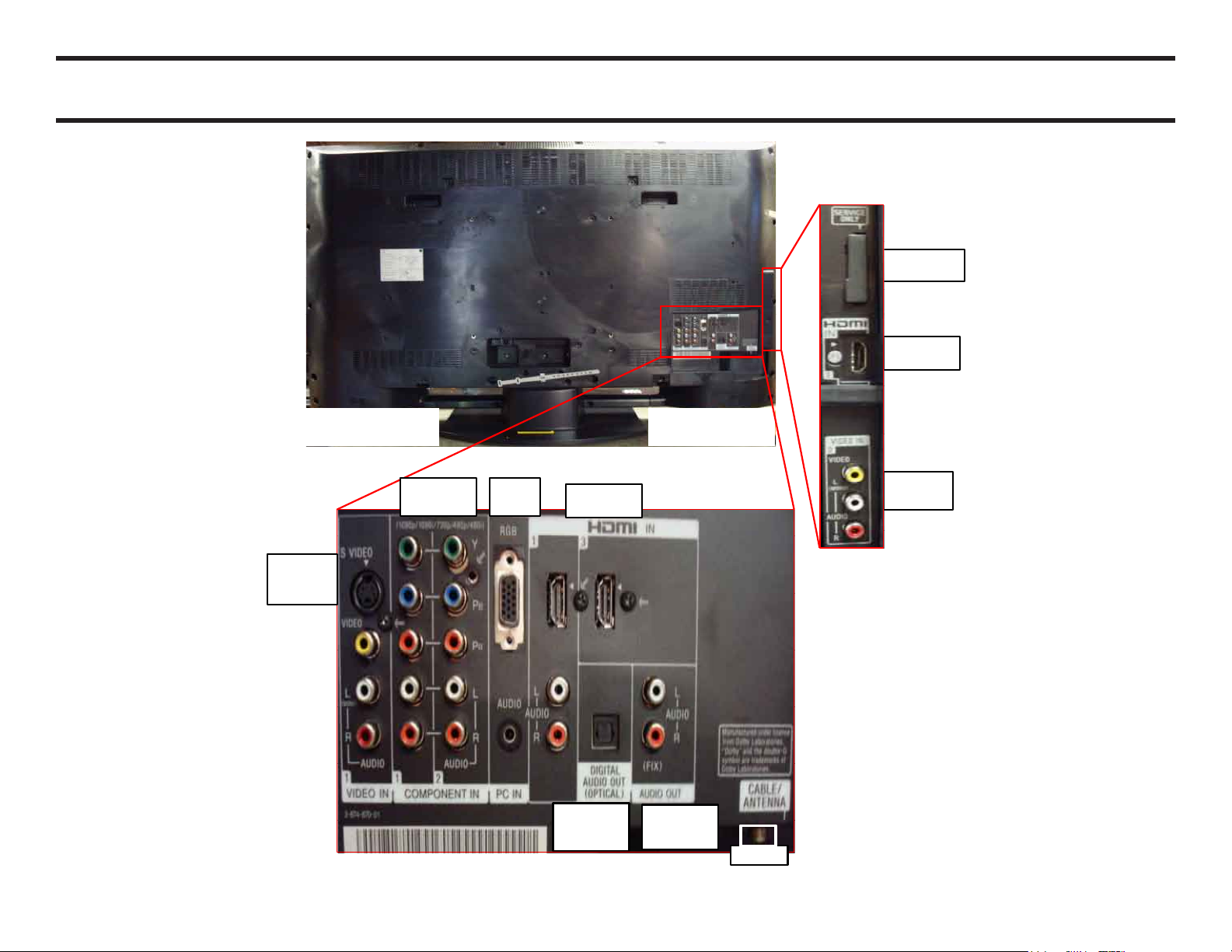
RF Input
Composite
&
S-Video
Input
Component
Inputs
PC
Inputs
Audio
Output
(FIXED)
Digital Audio
Output
(Optical)
HDMI & DVI
Inputs
Composite
Input
Service only
USB
HDMI & DVI
Input
CTV-47 3

Input & Output Layout and Description
Input Descriptions
RF Input
Reference Figure 1-1
Composite Video & Audio Inputs 1 & 2
Yellow Jack - Composite Video Input
Red & White Jacks - Right & Left Audio Input
Component Video & Audio Inputs 1 & 2
Red, Green, & Blue Jacks - Component Video Inputs
Red & White Jacks - Right & Left Audio Input
HDMI/DVI Video Inputs 1, 2, & 3 and DVI Audio
Both the HDMI and DVI formats contain digital video. In the case of the
HDMI format the audio is also digital and is part of the video and audio
data stream over the single HDMI connection. In contrast, the DVI format
contains only digital video in its data stream. The audio is sent over a
separate red and white wired analog audio connection. Furthermore, a
DVI to HDMI adapter is required to connect the DVI connector to the
HDMI connector.
Audio Outputs
Analog Fixed Audio Output
This audio output can be used to listen to the TV audio through an external
stereo system. The audio level at the output is set to a fixed level and
cannot be adjusted.
Digital Audio Output (Optical)
Connects to the optical audio input of any digital audio equipment that is
PCM/Dolby digital compatible. The following table shows the audio inputs
and the audio format which are present at the Optical Audio Output.
Audio Input Source Coaxial Output
Digital Tuner 5.1 (ATSC)
DVD HDMI 5.1 2CH PCM
All Analog Audio Inputs
Analog Tuner (NTSC)
SACD (HDMI) No Output
DVD Audio (HDMI)
2CH PCM
2CH PCM
2CH PCM
No Output
PC Video & Audio Input
The MA2 chassis models (KDl-26M4000, KDL-32M4000, KDL-37M4000,
and KDL-40M4000) have a Personal Computer Input (PC-IN), which
connects directly to the PC 15 pin DIN connector (HD15 connector). Once
connected the TV functions as a video monitor and audio output (separate
Stereo Mini Plug) for the PC. There is a complete table of PC Input Signal
Compatibility on Page 18 in the Owners Manual.
"Service Only" USB Connection
This USB connection is for Sony factory use only.
CTV-47 4
Section 2 - Chassis Layout
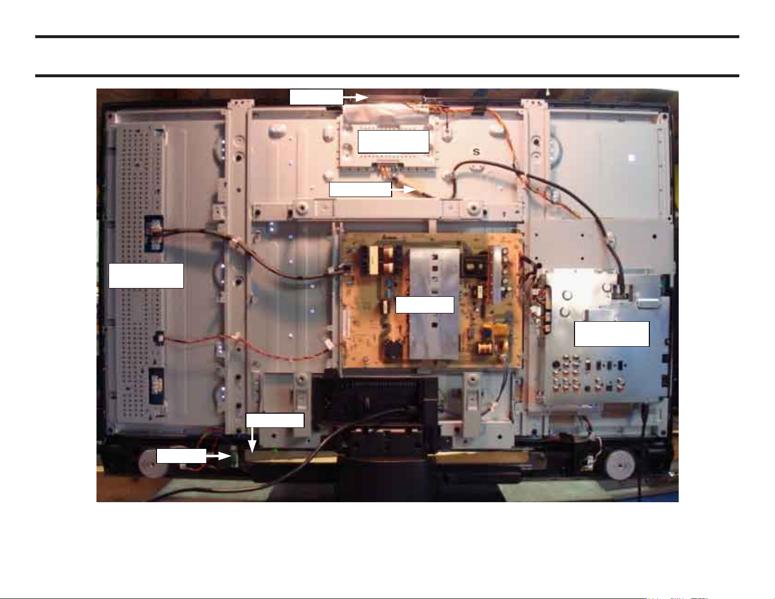
Balancer Board
(Under Cover)
G-Board
A-Board
(Under Shield)
TCON Board
(Under Shield)
H3-Board
LVDS Cable
H1-Board
H2-Board
KDL-40, 46S4100 PCB LAYOUT DIAGRAM
FIGURE 1-1
CTV-49 5
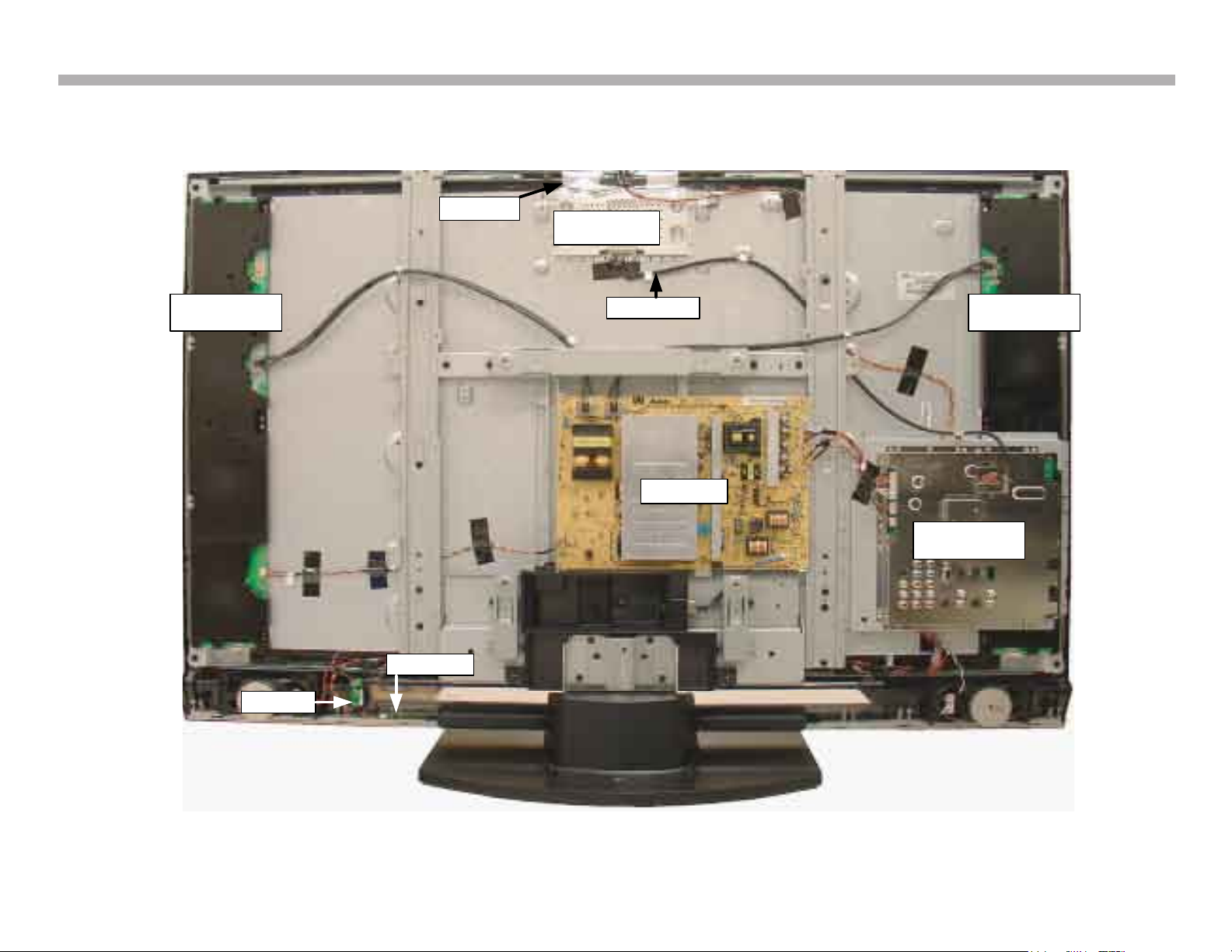
Chassis Layout
Balancer Board
(Under Cover )
G-Board
A-Board
(Under Shield )
TCON Board
(Under Shield )
H3-Board
LVDS Cable
H1-Board
H2-Board
Balancer Board
(Under Cover )
KDL-52S4100 PCB LAYOUT DIAGRAM
FIGURE 1-2
CTV-49 6

Chassis Layout
PCB and Component Descriptions
Reference Figures 1-1 & 1-2
A-Board
The circuits located on the A-Board perform all Video and Audio processing
functions. It also contains all the microprocessor control circuits. The
following circuits are included on this board.
• ATSC/NTSC Tuner
• TV Microprocessor
• HiDPRO IC
- A/V Processing
- Tuner RF Processing
- HDMI Processing
- Scan Converter
• Composite Input Terminals
• Component Input Terminals
• HDMI Input Terminals
• PC-IN Input Terminal
• RF/Cable Input Terminal
G-Board
Except for some regulator circuits on the A-Board, the G-Board is the
power supply system board, which includes the following components
and circuits.
• Standby Power Supply
o 3.3V
• Main Power Supply
o 15V
o 12V
o 6.5V
o 3.3V
• Backlight Inverter Circuit
o 1.1KV
• Power Factor Control (PFC)
• AC Relay
• Main Fuse (F1)
H1-Board
• Channel Up/Down Button
• Volume Up/Down Button
• TV/Video Button
• Menu Button
• Power Button
H2-Board
• IR Sensor
H3-Board
• Power LED
• Timer LED
• Standby LED
CTV-49 7

Balancer Board (Part of LCD Panel)
The Balancer Board takes the high voltage (1.1KV) from the backlight
inverter circuit on the G-Board and evenly spreads, and applies it to
each lamp for an even overall display brightness. Except for some lamp
current detection circuits the Balancer Board contains mostly passive
components. Lamp drive and current detection is mostly performed by
small transformers. There are two Balancer boards in the KDL-52S4100.
LCD Panel Assembly
The LCD Panel Assembly includes the LCD Panel, TCON, and Backlight
Lamps.
The LCD Panel contains the actual liquid crystals, color filters, and
polarizers. The liquid crystals are manipulated by the applied voltage to
pass a specific amount of light - from the backlight- depending on the level
of voltage applied. The panel resolution on all the FX chassis models is
1920 X 1080 lines. These are considered 1080P High-Definition models.
The TCON performs all the control, timing, charge, and discharge functions
driving the operation of the LCD Panel.
The Backlight Lamps generate the white light that passes through the
liquid crystals in the LCD Panel.
Chassis Layout
CTV-49 8
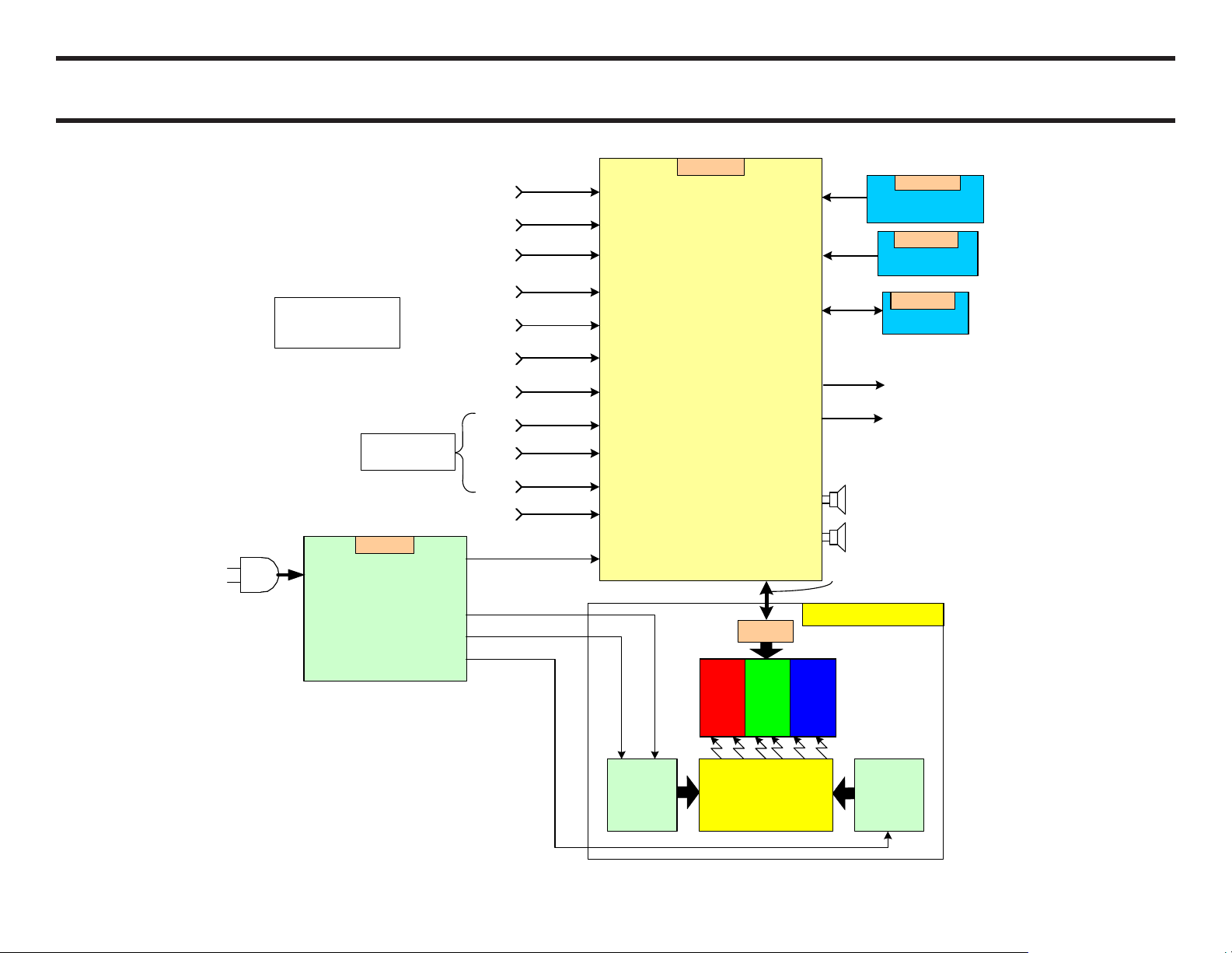
Overall Chassis Block Diagram
Standby 3.3V Power
Supply
Main Power Supply
Backlight Inverter
AC Relay
G-Board
AC
Input
Component 2
R
L
A-Board
ATSC/NTSC Tuner
TV Microprocessor
HiDPRO Processor :
Video Switching
A/V Processor
ATSC/NTSC Processing
HDMI
IP (Image Processor)
Scan Converter (Scalar)
Audio Processing
Audio Switching
Control Data
Power
LVDS Cable
Power
Keys
SIRCS
Power &
LED Control
LCD Pane l Assemble
Composite & S-Video 1
LCD PANEL
PC-IN
V
Digital
FIXED Audio Output
PC-IN Audio Input
Component 1
A/V &
S-Switch
Power Key
Function Keys
H1-Board
Optical Audio Output
HDMI 1
DVI Audio Input
RF/Cable
HDMI 2
A/V
Analog
A/V
Digital
A/V
Digital
A/V
Analog
A
Analog
A
Analog
CCFT
Backlights
A
Analog
A
Digital
A/V – Audio & Video
A – Audio Only
V – Video Only
Video Only for
DVI connection
RF
Composite Video 2
A/V
Analog
IR Sensor
H2-Board
H3-Board
LEDs
HDMI 3
A/V
Digital
Balancer
Board
(52")
Power
Balancer
Board
(40" & 46")
(52")
TCON
NOTE: The 40" & 46"
only have one Balancer
Board.
The 52" has two
Balancer Boards
Section 3 - Block Diagrams
CTV-49 9
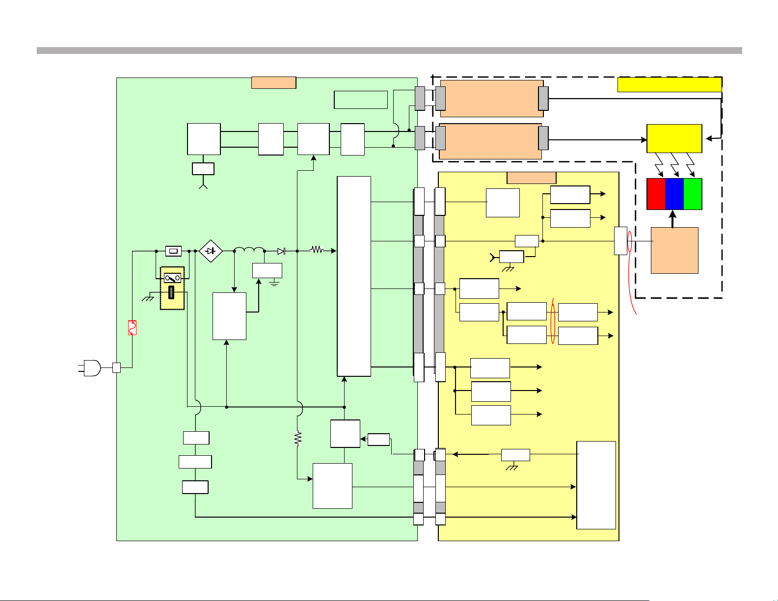
Power System Block Diagram
A-Board
15V
12V
0.08V
F1
AC
Input
BD1
RL1
NTC2
3.3VSB
IC801
PFC
L800
VCC
14V
D800
PS_ON
IC901
Standby
3.3V
Power
Supply
CN1
Switch
Circuit
Q901
14V
LCD
PANEL
CCFL
Backlights
TCON
LCD Panel Assembly
VCC
IC305
CN1101
CN301
Q3
Q4
U1105
1.8V REG
1.8V
Audio
Output
Amp
1.1KV
(2KV Strike Voltage)
CN12
LVDS Cable
G-Board
R915
Panel 12V
6.5V
14V
1.2V
1.8V
5V
Power_On
CN302
U2903
TV
Micro
0V
3V
15V
Q2504
PANEL_EN
7
&
3
6
Q903
IC306
Q305
AC_OFF_DET 0V
3.3VSB
3.3V
CN501 & CN502
HV1
Balancer Board
(40" & 46")
(52")
HV2
T301
12V
DRV1
DRV2
Q904
T302
HV1 – 1.1KV
HV2 – 1.1KV
IC706
Q301
Q310
Q800
R614
IC601
Main
Power
Supply
VCC
U1108
1.8V REG
U1107
1.2V REG
7
/
9
5
9
U1109
5V Reg
U1104
5V REG
U1502
3.3V REG
U1106
1.2V REG
U2102
3.3V REG
U2103
1.2V REG
Q2502
U1102
9V REG
U1103
8V REG
1
&
2
11
&
12
13
1
9V
8V
3.3V
5V
1.2V
1.2V
Q1101
1
5,7
9,11
13
1
4
&
5
2
3
/
5
CN1102
12V
Balancer Board
(52")
1.1KV
(2KV Strike Voltage)
Block Diagrams
CTV-49 10
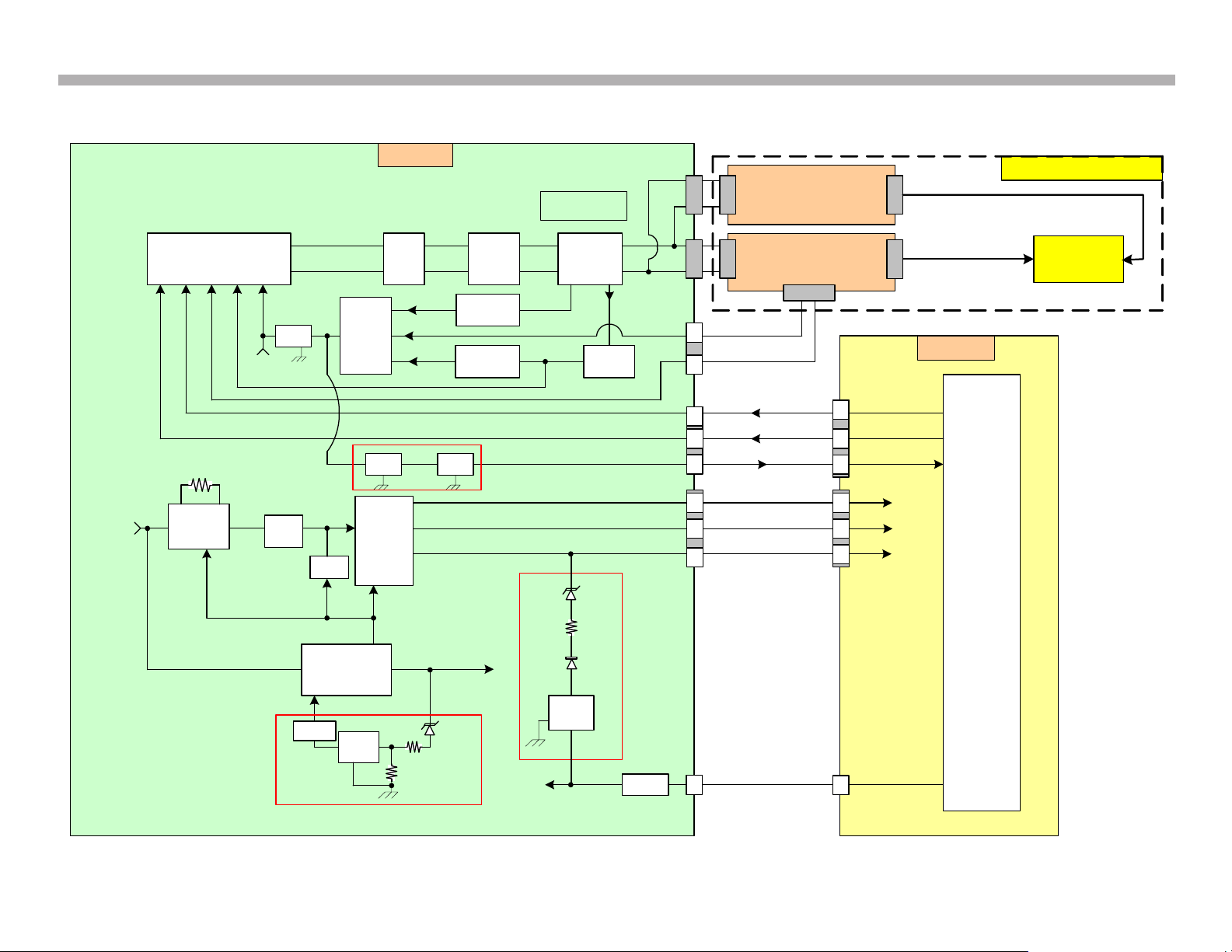
Protection Circuits Block Diagram
PFC
RL1
Inrush
Relay
BD1
AC
Input
STBY 3.3V
NTC1
VCC
G-Board
Q309
VCC
14
V
R351
To
IC601, PFC,
RL
1
7
CN503
CN302
CN501 & CN502
T301
DRV
1
DRV
2
T302
HV1 – 1.1KV
HV2
– 1.1KV
IC706
Inverter Controller
Q301
Q310
HV
Detect
HV OCP
ARC
Protect
IC701
SW
LD
FB
6
2
CN503
Dimmer
Enable
Q708
12V
OVP
BL-DET
Q704
Q705
Backlight
Detect
A-Board
IC2903
TV Micro
11
12V
BL-DET
PS
-ON
IC601
Main
Power
Supply
6.5V
2X
5X
4
2
1
2
5
4
5
13
1
9
BL
-ONBL-ON
CN303
CN1101
CN2502
Q306
SCR
Q910
SCR
IC952
ZD306
ZD905
D314
R933
STBY 3.3V
OVP
IC901
Standby
3.3V
Power Supply
R940
PS
-ON
0V
0V
11
V
3V
Min
1.4V
Max 3.2V
13
13
3.3V
CCFL
Backlights
LCD Panel Assembly
1.1KV
(
2KV Strike Voltage)
Balancer Board
(40" & 46")
(52")
Balancer Board
(52")
1.1KV
(
2KV Strike Voltage)
Block Diagrams
CTV-49 11
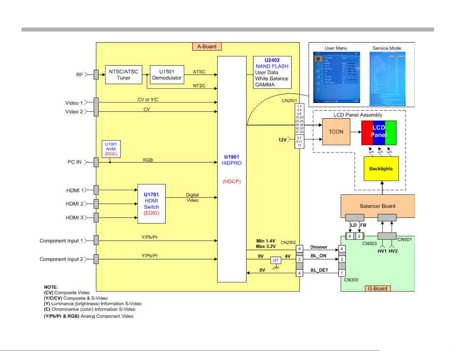
Video System Block Diagram
Block Diagrams
CTV-49 12
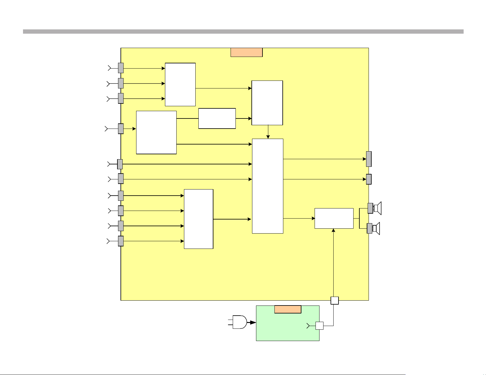
Audio System Block Diagram
Video 2
Video 1
U2601
Audio
Switch
LR Audio
A-Board
U1901
HiDPRO
HDMI 2
Component Input 2
RF
PC IN
LR Audio
15V
CN201
HDMI 3
Component Input 1
U1701
HDMI
Switch
NTSC/ATSC
Tuner
Digital
Audio
ATSC
NTSC (Audio)
G-Board
R
L
CN14
LR Audio
Analog Audio Output
(FIXED)
Digital Audio Outpurt
(Optical)
LR Audio
SPDIF
DVI Audio IN
LR Audio
LR Audio
LR Audio
I2S
CN1
CN2601
CN2801
1
1
AC
U2701
Output Amplifier
I2S
CN13
U2602
Audio
Processor
I2S (ATSC & HDMI Audio)
U1501
Demodulator
HDMI 1
Block Diagrams
CTV-49 13
 Loading...