

Sony KDL-40R455 Schematic
HISTORY INFORMATION FOR THE FOLLOWING MANUAL:
Self Diagnosis
Supported model
SERVICE MANUAL
ELECTRICAL SERVICE INTERNAL DISTRIBUTION ONLY
MODEL COMMANDER DESTINATION
KDL-24R400A RM-YD092 Mexico / Latin America
KDL-24R405A RM-YD093 Chile / Peru / Venezuela
KDL-24R407A RM-YD093 Colombia
KDL-32R400A RM-YD093 US / Canada
KDL-32R400A RM-YD092 Mexico / Latin America
KDL-32R405A RM-YD093 Chile / Peru / Venezuela
KDL-32R407A RM-YD093 Colombia
KDL-32R421A RM-YD092 Mexico
KDL-32R425A RM-YD093 Chile / Peru / Venezuela
RB1FK
Segments: BA
CHASSIS
KDL-40R450A RM-YD092 US / Canada
KDL-40R450A RM-YD092 Mexico / Latin America
KDL-40R471A RM-YD092 Mexico
KDL-40R457A RM-YD093 Colombia
KDL-40R455A RM-YD093 Chile / Peru / Venezuela
KDL-40R475A RM-YD093 Chile / Peru
KDL-46R450A RM-YD092 Mexico / Latin America
KDL-46R450A RM-YD092 Canada
KDL-46R455A RM-YD093 Chile / Peru / Venezuela
KDL-46R457A RM-YD093 Colombia
KDL-46R471A RM-YD092 Mexico
LEVEL
CONFIDENTIAL
3
ORIGINAL MANUAL ISSUE DATE: 11/2013
REVISION DATE SUBJECT
11/15/2013 Original Manual Release Date
9-883-556-51
LCD DIGITAL COLOR TV

Chassis: RB1FK, BA
TABLE OF CONTENTS
SECTION TITLE PAGE
SECTION 1: DIAGRAMS ................................................................................................................................................................................................... 3
1-1. Printed Circuit Boards and Schematic Diagrams Information .................................................................................................................... 3
1-2. Connector Diagrams ........................................................................................................................................................................................ 4
1-3. Main Board (A Board) ...................................................................................................................................................................................... 5
A Board Component Side ................................................................................................................................................................................5
A Board Conductor Side ..................................................................................................................................................................................6
A Board Schematic
1-4. Electrical Parts List / Main Board (A) .......................................................................................................................................................... 27
..........................................................................................................................................................................................7
SECTION 2: POWER SUPPLY BOARD (G BOARD)
G Board Component Side .............................................................................................................................................................................28
G Board Schematic
SECTION 3: IR BOARD (H BOARD)
H Board Component Side ..............................................................................................................................................................................30
H Board Conductor Side ...............................................................................................................................................................................30
H Board Schematic
APPENDIX A: ENCRYPTION KEY COMPONENTS
........................................................................................................................................................................................ 29
..............................................................................................................................................................................30
..........................................................................................................................................................................................31
..................................................................................................................................................... 28
..................................................................................................................................................... A-1
Chassis: RB1FK, BA 2
Chassis: RB1FK, BA
CAUTIONS AND WARNINGS
CAUTION
. To reduce the risk of electric shock, do not
WARNING!!
An isolation transformer should be used during any service to avoid possible shock hazard, in case of live chassis.
!
SAFETY-RELATED COMPONENT WARNING!!
shading and
NOTE: Do not modify the original design without obtaining written permission from the manufacturer or you will void the
original parts and labor warranty.
!
mark on the schematic diagrams and the parts list. It is essential that these critical parts be replaced only
ATTENTION!!
ainsi.
ALERTE!!
lors de tout dépannage.
!
ATTENTION AUX COMPOSANTS
RELATIFS A LA SECURITE!!
!
sur les schemas de principe, les vues explosees et
les listes de pieces sont d’une importance critique pour la securite du fonctionnement. Ne les remplacer que par des
composants Sony dont le numero de piece est indique dans le present manuel ou dans des supplements publies par
present manuel. Suivre ces procedures lors de chaque remplacement de composants critiques, ou lorsqu’un mauvais
fonctionnement suspecte.
Chassis: RB1FK, BA 3
Chassis: RB1FK, BA
When installing the LCD panel on a wall, the LCD panel must be secured using the 4 mounting holes on the rear
, or volatile solvent, such as
TV screen . If liquid drips into the bottom of the screen it may
SETTING UP AND CARRYING THE TV
• Disconnect all cables when carrying the TV.
• Carry the TV with the adequate number of people; larger size TVs require two or more people.
• Correct hand placement while carrying the TV is very important for safety and to avoid damage.
USE CAUTION WHEN HANDLING THE LCD PANEL
When repairing the LCD panel, be sure you are grounded by using a wrist band.
cover.
To avoid damaging the LCD panel:
1. Do not press on the panel or frame edge to avoid the risk of electric shock.
2. Do not scratch or press on the panel with any sharp objects.
3. Do not leave the module in high temperatures or in areas of high humidity for an extended period of time.
4. Do not expose the LCD panel to direct sunlight.
5. Avoid contact with water. It may cause a short circuit within the module.
6. Disconnect the AC power when replacing the backlight (CCFL) or inverter circuit.
(High voltage occurs at the inverter circuit at 650Vrms.)
7. Always clean the LCD panel with a soft cloth material.
8. Use care when handling the wires or connectors of
the inverter circuit. Damaging the wires may cause a
short.
9. Protect the panel from ESD to avoid damaging the
electronic circuit (C-MOS).
10. During the repair,
more than 1 hour
cloth.
DO NOT leave the Power On for
while the TV is face down on a
CLEANING THE LCD PANEL
CAUTION: When cleaning the TV, be sure to unplug the power cord to avoid any chance of electric shock.
Clean the cabinet of the TV with a dry soft cloth.
Wipe the LCD screen gently with a soft cloth.
Stubborn stains may be removed with a cloth slightly moistened with a solution of mild soap and warm water.
If using a chemically pretreated cloth, please follow the instruction provided on the package.
Never use strong solvents such as a thinner, alcohol or benzine for cleaning.
Periodic vacuuming of the ventilation openings is recommended to ensure proper ventilation.
Do Not use paper towels, any type of abrasive pad, rags, rubber or vinyl materials to clean the screen. Using
these materials could easily scratch the screen which may result in permanent damage.
Do Not use any cleaning product containing alkaline/acid cleaner, scouring powder
alcohol, ammonia, benzine, thinner or insecticide. Using any of these harsh cleaners may result in permanent
damage to the screen.
Do Not spray water or detergent directly onto the
cause a failure.
Chassis: RB1FK, BA 4
SAFETY CHECK-OUT
Trouble Light
Chassis: RB1FK, BA
After correcting the original service problem, perform the
following safety checks before releasing the set to the
customer:
1. Check the area of your repair for unsoldered or
poorly soldered connections. Check the entire
board surface for solder splashes and bridges.
2. Check the interboard wiring to ensure that no
wires are “pinched” or touching high-wattage
resistors.
3. Check that all control knobs, shields, covers,
ground straps, and mounting hardware have been
replaced. Be absolutely certain that you have
replaced all the insulators.
4. Look for unauthorized replacement parts,
particularly transistors, that were installed during
a previous repair. Point them out to the customer
and recommend their replacement.
5. Look for parts which, though functioning, show
obvious signs of deterioration. Point them out to
the customer and recommend their replacement.
6. Check the line cords for cracks and abrasion.
Recommend the replacement of any such line
cord to the customer.
7. Check the antenna terminals, metal trim,
“metallized” knobs, screws, and all other exposed
metal parts for AC leakage. Check leakage as
described in “Leakage Test”.
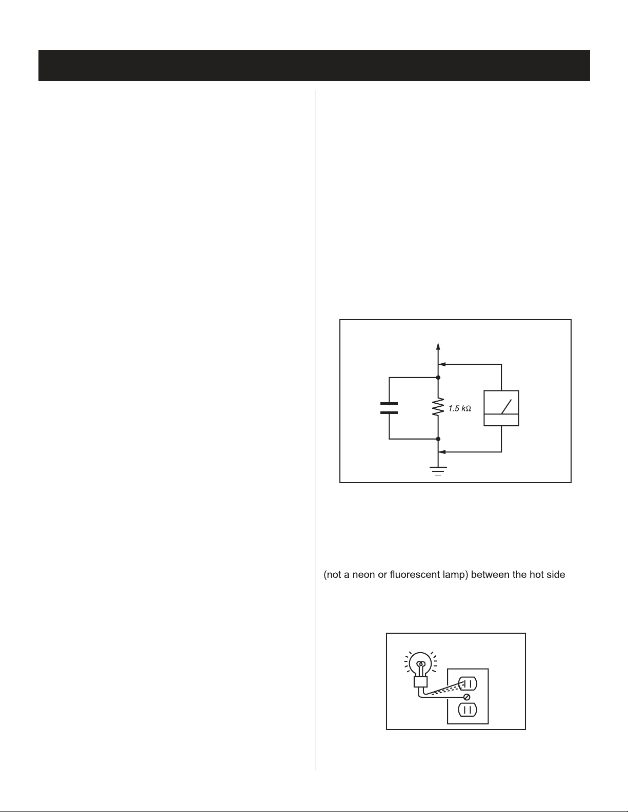
LEAKAGE TEST
The AC leakage from any exposed metal part to earth
ground and from all exposed metal parts to any exposed
metal part having a return to chassis, must not exceed
0.5 mA (500 microamperes). Leakage current can be
measured by any one of three methods.
1. A commercial leakage tester. Follow the
manufacturers’ instructions provided with the
tester.
2. A battery-operated AC milliammeter.
3. Measuring the voltage drop across a resistor
by means of a VOM or battery-operated AC
voltmeter. The “limit” indication is 0.75 V, so
analog meters must have an accurate low
voltage scale. Nearly all battery-operated digital
multimeters that have a 2 VAC range are suitable.
(see Figure A)
To Exposed Metal
Parts on Set
AC
0.15 µF
Voltmeter
(0.75V)
Chassis: RB1FK, BA 5
Earth Ground
Figure A. Use an AC voltmeter to check AC leakage.
HOW TO FIND A GOOD EARTH GROUND
The cover-plate retaining screw on most AC outlet boxes
is at earth ground. Verify the AC outlet box retaining screw
ground by connecting a 60W to 100W incandescent
of the receptacle and the retaining screw. Try both slots,
if necessary, to locate the hot side on the line; the lamp
should light at normal brilliance if the screw is at ground
potential. (see Figure B)
AC Outlet Box
Figure B. Checking for earth ground.
Chassis: RB1FK, BA
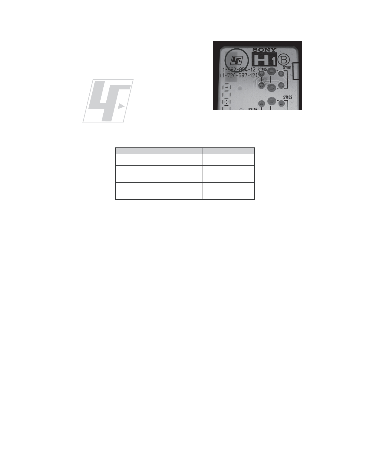
Th
e circuit boards used in these models have been processed using
Due
This
Lead Free Solder. The boards are identified by the LF logo located
close to the board designation e.g. H1 etc [ see example ]. The
servicing of these boards requires special precautions to be taken as
outlined below.
example
It is strongly recommended to use Lead Free Solder material in order to guarantee optimal quality of new solder joints.
Lead Free Solder is available under the following part numbers :
rebmuntraP retemaiD skrameR
91-500-046- m7 m3. g0 K52.0
02-500-046- m7 m4. g0 K05.0
12-500-046- m7 m5. g0 K05.0
22-500-046- m7 m6. g0 K52.0
32-500-046- m7 m8. g0 K00.1
42-500-046- m7 m0. g1 K00.1
52-500-046- m7 m2. g1 K00.1
62-500-046- m7 m6. g1 K00.1
to the higher melting point of Lead Free Solder the soldering iron tip temperature needs to be set to 370 degrees celsius.
requires soldering equipment capable of accurate temperature control coupled with a good heat recovery characteristics.
Chassis: RB1FK, BA 6
Chassis: RB1FK, BA
Terminal name of semiconductors in silk screen
SECTION 1: DIAGRAMS
1-1. PRINTED CIRCUIT BOARDS AND SCHEMATIC DIAGRAMS INFORMATION
REFERENCE INFORMATION
All capacitors are in µF unless otherwise noted. pF : µµF 50WV or
less are not indicated except for electrolytics and tantalums.
$OOHOHFWURO\WLFVDUHLQ9XQOHVVRWKHUZLVHVSHFL¿HG
All resistors are in ohms. k:=1000:, M:=1000k
:
Indication of resistance, which does not have one for rating
electrical power, is as follows: Pitch : 5mm
Rating electrical power :
1
/4 W in resistance, 1/
W and 1/
10
W in chip resistance.
16
1
/4 W
QRQÀDPPDEOHUHVLVWRU
IXVLEOHUHVLVWRU
RESISTOR
: RN METAL FILM
: RC SOLID
: FPRD NONFLAMMABLE CARBON
: FUSE NONFLAMMABLE FUSIBLE
: RW NONFLAMMABLE WIREWOUND
: RS NONFLAMMABLE METAL OXIDE
: RB NONFLAMMABLE CEMENT
: ADJUSTMENT RESISTOR
COIL
: LF-8L MICRO INDUCTOR
: internal component
: panel designation and adjustment for repair
: earth ground
printed circuit ( )
Device Printed symbol Terminal name
Transistor
1
*
: earth-chassis
Transistor
2
All variable and adjustable resistors have characteristic curve B, unless
3
Diode
Cathode
otherwise noted.
4
5HDGLQJVDUHWDNHQZLWKDFRORUEDUVLJQDOLQSXW
Readings are taken with a 10M: digital multimeter.
Voltages are DC with respect to ground unless otherwise noted.
Diode
Diode
5
Diode
6
9ROWDJHYDULDWLRQVPD\EHQRWHGGXHWRQRUPDOSURGXFWLRQ
Diode
tolerances.
All voltages are in V.
60HDVXUHPHQWLPSRVVLELOLW\
: B+line.
%OLQH$FWXDOPHDVXUHGYDOXHPD\EHGLIIHUHQW
: signal path. (RF)
&LUFOHGQXPEHUVDUHZDYHIRUPUHIHUHQFHV
7KHFRPSRQHQWVLGHQWL¿HGE\ VKDGLQJDQG!V\PERODUHFULWLFDO IRUVDIHW\5HSODFH
RQO\ZLWKSDUWQXPEHUVSHFL¿HG
7KHV\PERO
LQGLFDWHVDIDVWEORZIXVH DQGLV GLVSOD\HGRQWKHFRPSRQHQW
VLGHRIWKHERDUG5HSODFHRQO\ZLWKIXVHRIWKHVDPHUDWLQJDVPDUNHG
127(7KHFRPSRQHQWVLGHQWL¿HG E\DUHGRXWOLQHDQGD PDUNFRQWDLQFRQ¿GHQWLDO
LQIRUPDWLRQ6SHFL¿FLQVWUXFWLRQVPXVWEHDGKHUHGWRZKHQHYHUWKHVHFRPSRQHQWV
are repaired and/or replaced.
6HH$SSHQGL[$(QFU\SWLRQ.H\&RPSRQHQWVLQWKHEDFNRIWKLVPDQXDO
Chassis: RB1FK, BA 7
7
8
Diode
Diode
9
Diode
10
Diode
11
Diode
12
Transistor
13
(FET)
Transistor
14
(FET)
Transistor
15
(FET)
Transistor
16
Transistor
17
Transistor
18
Transistor
19
Transistor
20
Transistor
21
Transistor
22
Transistor
23
Discrete semiconductor
–
(Chip semiconductors that are not actually used are included.)
Anode
Anode
Anode
Anode Cathode
Anode
Anode Anode
Cathode
Cathode
Anode
Anode
Cathode
CAPACITOR
: TA TANTALUM
: PS STYROL
: PP POLYPROPYLENE
: PT MYLAR
: MPS METALIZED POLYESTER
: MPP METALIZED POLYPROPYLENE
: ALB BIPOLAR
: ALT HIGH TEMPERATURE
: ALR HIGH RIPPLE
Collector
Base
Collector
Base
Cathode
Cathode
Common
Common
Common
Common
Common
Common
Drain
Drain
C2
C1
E1
E2
C2
B1
E2
C2
Emitter
Emitter
(NC)
(NC)
Cathode
Anode
Cathode
Cathode
Cathode
Anode
Anode
Source
Gate
Source
Gate
Source
Drain
Gate
Emitter
Collector
Base
B1 E1
B2 C1E2
B2 E2
B1 C2
B2 E2C1
B1 C2E1
B2 E2C1
B1 C2E1
B1 E1
C1(B2)
(B2)
E1
E2
C2C1
(B2)
E1
B1
C1
Anode
Circuit
D
G
D
S
B1
B1
B1
B1
B1
B1
D
G
S
S
D
G
S
C2
C1
B2
E1
E2
C2
C1
B2
E1
E2
E2B2E1
C1
C2
C2C1(B2)
E2
E2
E2E1(B2)
C1
C2
C2E1(B2)
C1
C2
Ver.1.6
G
Chassis: RB1FK, BA 8
Chassis: RB1FK, BA
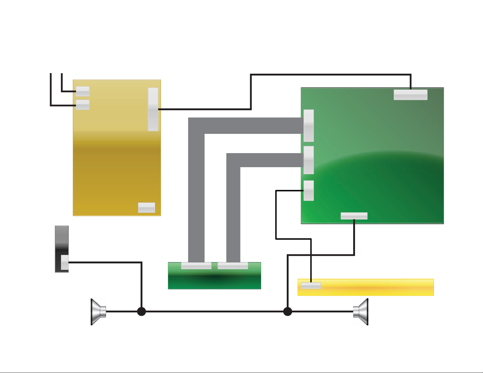
1-2. CONNECTOR DIAGRAMS
TCON Board
CN4001
CN201
CN4002
CN4003
AC
Main Board
IR Board
Power Board
Keypad Board
LCD Panel
CN8001
A
A
—
B
—
C
Chassis: RB1FK, BA
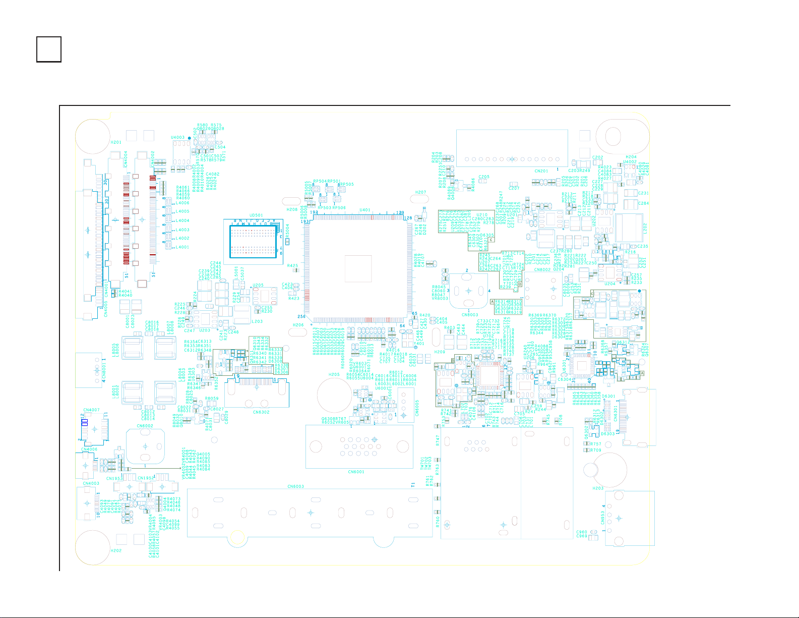
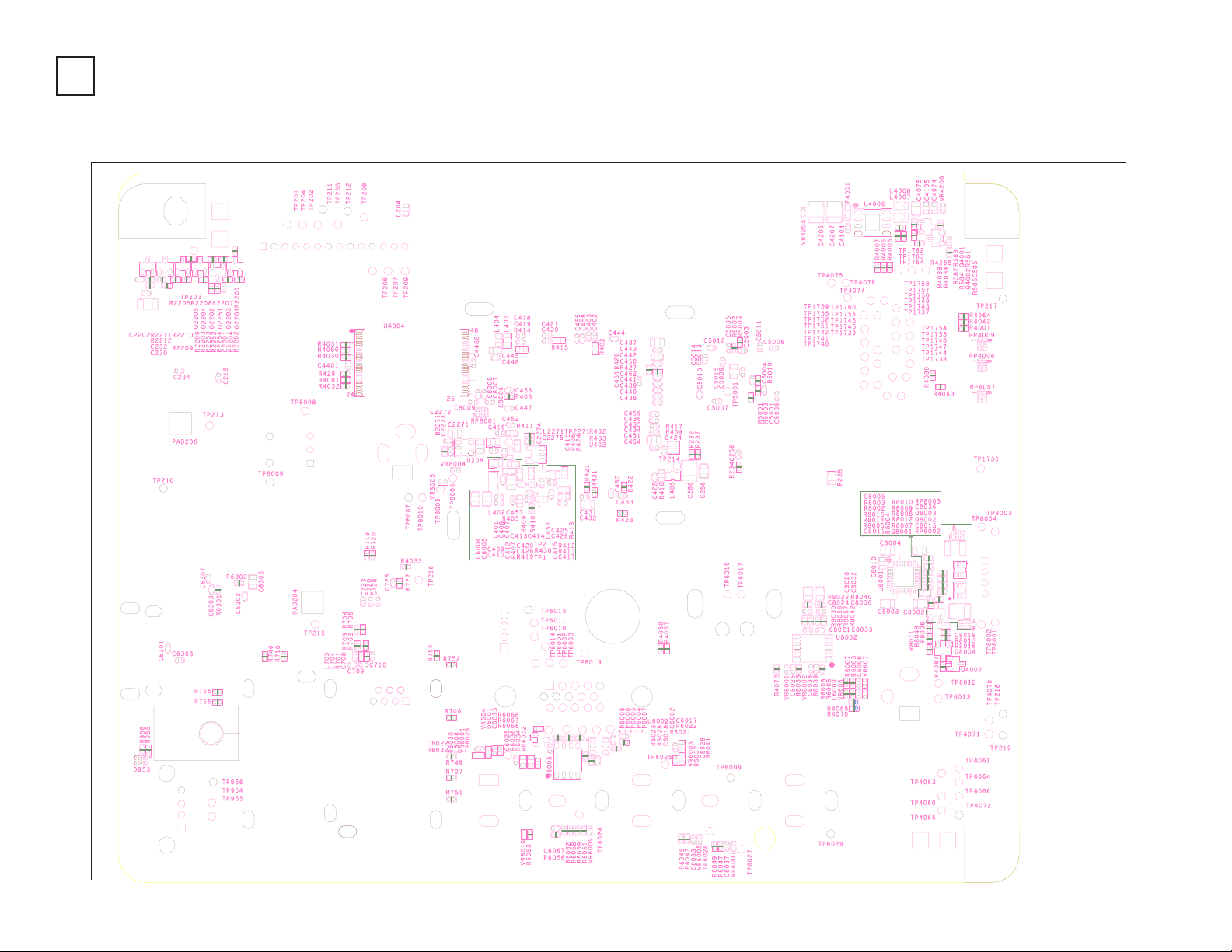
1-3. MAIN BOARD (A BOARD)
[SYSTEM POWER/YPBPR/AV/SPDIF/USB/HDMI/DDR/FLASH/PREAMP/AUDIO AMP/LVDS/DEMOD/TUNER/ETHERNET]
A BOARD COMPONENT SIDE
1 | 2 | 3 | 4 | 5 | 6 | 7 | 8 | 9 | 10 |
—
D
—
E
—
F
—
Chassis: RB1FK, BA 9
Chassis: RB1FK, BA
A
A
—
B
—
C
—
[SYSTEM POWER/YPBPR/AV/SPDIF/USB/HDMI/DDR/FLASH/PREAMP/AUDIO AMP/LVDS/DEMOD/TUNER/ETHERNET]
A BOARD CONDUCTOR SIDE
1 | 2 | 3 | 4 | 5 | 6 | 7 | 8 | 9 | 10 |
D
—
E
—
F
—
Chassis: RB1FK, BA 10
Chassis RB1FK, BA 11
Chassis RB1FK, BA
A BOARD SCHEMATIC
A BOARD SCHEMATIC DIAGRAM (1 OF 20)
1
1
2
2
3
3
4
4
5
5
6
6
7
7
8
8
A A
B B
C
C
D
D
E E
F F
G G
H H
Title
veRrebmuN tnemucoDeziS
teehS:etaD
of
FY13 BA_MT5389
A
Block Diagram
A3
2 21Thursday, December 20, 2012
Title
veRrebmuN tnemucoDeziS
teehS:etaD
of
FY13 BA_MT5389
A
Block Diagram
A3
2 21Thursday, December 20, 2012
Title
veRrebmuN tnemucoDeziS
teehS:etaD
of
FY13 BA_MT5389
A
Block Diagram
A3
2 21Thursday, December 20, 2012
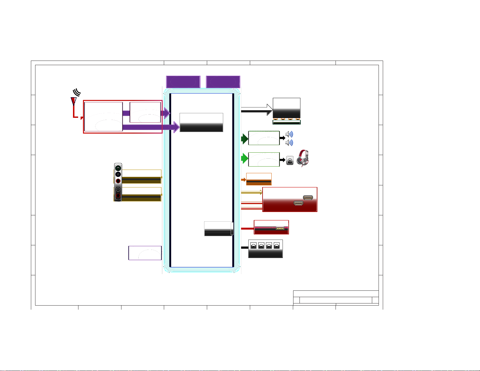
DDR3x1
(1GB)
MT5367/5389
Ypbpr/CVBS
Ypbpr-R/L/CVBS-R/L
IR LED Keypad
USB(Side)
HDMI1/MHL (Side)
SPDIF
HP Driver
Amplifier
Speaker
:
R
L
Headphone/Line out
LVDS
12S
IF
TS
IF
LCM Panel
HDMI2(ARC)
86%
NAND Flash
64 MB
S-Tuner
RE227TN(PAD)
RA227TN(NA/MX)
RB221TN(COL/CHI)
DEMO
CXD2817ER(PAD)
CXD2837ER(COL)
CXD2838ER(CHI)
Demodulador
PAL/SECAM/ATSC
Chassis RB1FK, BA 12
Chassis RB1FK, BA
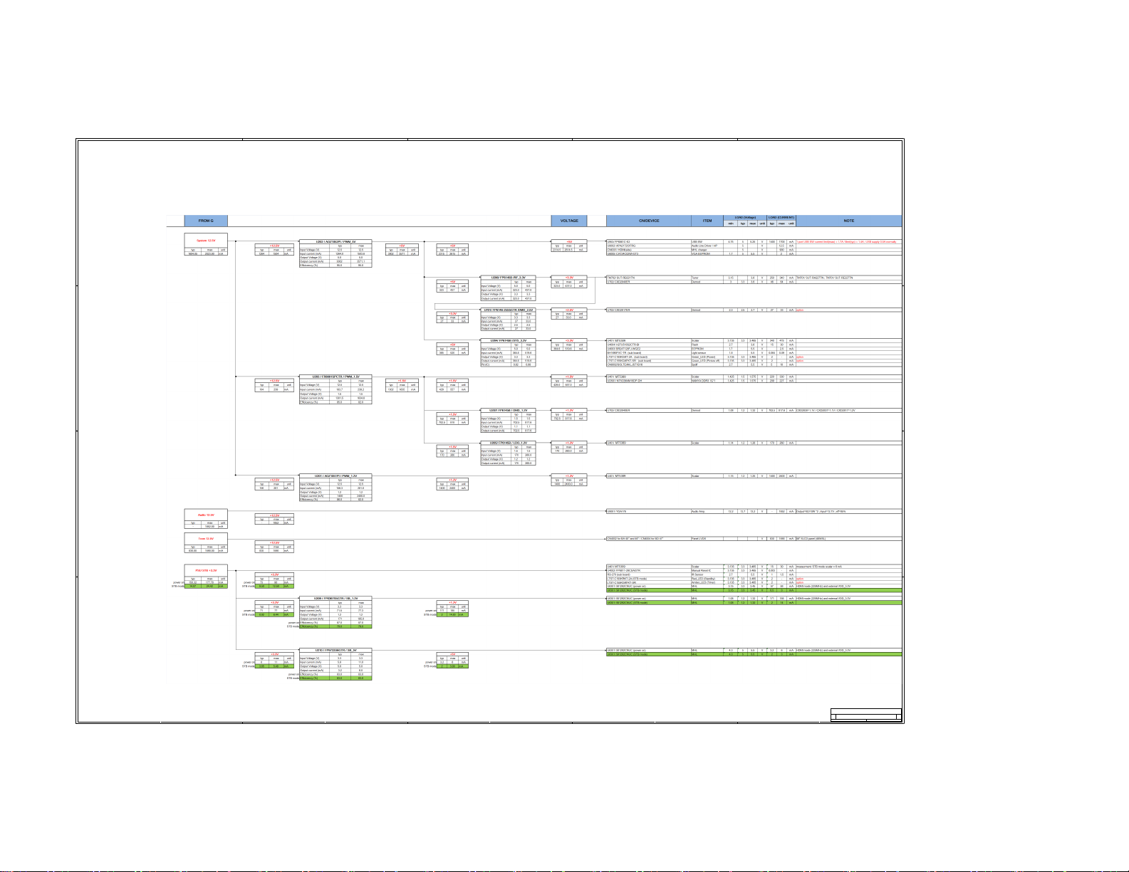
A BOARD SCHEMATIC DIAGRAM (2 OF 20)
5
5
4
4
3
3
2
2
1
1
D
D
C
C
B
B
A
A
Title
veRrebmuN tnemucoDeziS
teeh
S
:et
aD
of
FY13 BA_MT5389
A
Power Structure
A0
3 21Thursday, February 28, 2013
Title
veRrebmuN tnemucoDeziS
teeh
S
:et
aD
of
FY13 BA_MT5389
A
Power Structure
A0
3 21Thursday, February 28, 2013
Title
veRrebmuN tnemucoDeziS
teeh
S
:et
aD
of
FY13 BA_MT5389
A
Power Structure
A0
3 21Thursday, February 28, 2013
 Loading...