

Page 1
HISTORY INFORMATION FOR THE FOLLOWING MANUAL:
Self Diagnosis
Supported model
SERVICE MANUAL
ELECTRICAL SERVICE INTERNAL DISTRIBUTION ONLY
MODEL COMMANDER DESTINATION
KDL-32W700B RM-YD103 US / Canada
KDL-32W700B RM-YD103 Mexico / Latin America
KDL-42W700B RM-YD103 US / Canada
KDL-42W800B RM-YD103 Mexico / Latin America
KDL-42W805B RM-YD099 Brazil
KDL-50W700B RM-YD103 US / Canada
KDL-50W790B RM-YD102 US / Canada
KDL-50W800B RM-YD102 US / Canada
KDL-50W800B RM-YD102 Mexico / Latin America
KDL-50W805B RM-YD099 Argentina
KDL-50W805B RM-YD099 Brazil
RB2G
Segment: HE-L
CHASSIS
KDL-50W805B RM-YD099 Chile / Peru / Ecuador
KDL-50W807B RM-YD099 Colombia
LEVEL
CONFIDENTIAL
3
KDL-55W700B RM-YD103 US / Canada
KDL-55W790B RM-YD102 US / Canada
KDL-55W800B RM-YD102 US / Canada
KDL-55W800B RM-YD102 Mexico / Latin America
KDL-55W805B RM-YD099 Brazil
KDL-55W805B RM-YD099 Chile / Peru
KDL-55W807B RM-YD099 Colombia
ORIGINAL MANUAL ISSUE DATE: 2/2015
REVISION DATE SUBJECT
2/6/2015 Original Manual Release Date
9-883-559-51
LCD DIGITAL COLOR TV
Page 2

Chassis: RB2G, HE-L
TABLE OF CONTENTS
SECTION TITLE PAG E
SECTION 1: DIAGRAMS ................................................................................................................................................................................................... 8
1-1. Printed Circuit Boards and Schematic Diagrams Information ............................................................................................................................ 8
SECTION 1: DIAGRAMS ................................................................................................................................................................................................... 9
1-2. Circuit Boards Location ...................................................................................................................................................................................... 9
SECTION 2: TROUBLESHOOTING ................................................................................................................................................................................ 10
2.1-1 - No Power: General ........................................................................................................................................................................................10
2.1-2 - No Power: AC Adaptor .................................................................................................................................................................................. 10
2.1-3 - No Power: DC/DC Converter Check ............................................................................................................................................................. 11
2.1-4 - No Power: Ayu2 Control ................................................................................................................................................................................15
2.1-5 - No Power: G Board ....................................................................................................................................................................................... 22
2.1-6 - No Power: DC/DC Converter Check ............................................................................................................................................................. 23
2.1-7 - No Power: Ayu2L Control .............................................................................................................................................................................. 25
2.1-8 - No Power: Ayu2 / Ayu2L Failure ....................................................................................................................................................................28
2.1-9 - No Power: Ayu2 / Ayu2L Replacement .........................................................................................................................................................29
2.2-1 - Led Blinking: 3X DC Alert & Communication Error .......................................................................................................................................30
2.2-2 - Led Blinking: 3X (Audio Error) - BAX-L (HE-L,HM,HE-H) Board Only ..........................................................................................................39
2.2-3 - Led Blinking: 4X Led Voltage Error ...............................................................................................................................................................42
2.2-4 - Led Blinking: 5X T-CON Error .......................................................................................................................................................................43
2.2-5 - Led Blinking: 6X Backlight Error ....................................................................................................................................................................46
2.2-6 - Led Blinking: 7X Temperature Error .............................................................................................................................................................. 49
2.3-1 - No Sound: General .......................................................................................................................................................................................51
2.3-2 - No Sound: Audio (For All Models) TUS and BAX (HT-L, HT-H, HT-H65, HS) ............................................................................................... 52
2.3-3 - No Sound: Audio (For All Models) BAX-L (HE-L, HM, HE-H) Board Only ..................................................................................................... 56
2.3-4 - No Sound: Main Board Power Off Checking (Main Speaker L & R) For BAX-L (HEL, HEH, HM) Board Only ............................................. 59
2.3-5 - No Sound: Main Board Power Off Checking (Main Speaker L & R) For BAX-L (HEL, HEH, HM) Board Only ............................................. 61
2.3-5 - No Sound: Main Board Power Off Checking (Main Speaker L & R) For BAX-L (HEL, HEH, HM) Board Only ............................................. 62
2.3-6 - No Sound: HP/Lineout Only For BAX-L (HEL, HEH, HM) Board Only .......................................................................................................... 68
2.3-7 - No Sound: Tuner ...........................................................................................................................................................................................71
2.3-8 - No Sound: HDMI ........................................................................................................................................................................................... 72
2.3-9 - No Sound: MHL .............................................................................................................................................................................................73
2.4 - RB2 Analog Signal Path ...................................................................................................................................................................................76
2.5-1 - No Picture: (BAX + TUS) ............................................................................................................................................................................... 77
2.5-2 - No Picture: Input Skip Function - BAX/BAX-L ............................................................................................................................................... 78
2.5-3 - No Picture: Tuner ..........................................................................................................................................................................................79
2.5-4. Tuner COL-T2 / BRZ / ARG ............................................................................................................................................................................ 86
2.5-5 - No Picture: HDMI ..........................................................................................................................................................................................99
2.5-6 - No Picture: HDMI (BAX-L & BAX Board) ....................................................................................................................................................102
2.5-7 - No Picture: MHL (BAX-L) ............................................................................................................................................................................108
2.5-8 - No Picture: MHL (BAX) ............................................................................................................................................................................... 11 0
2.5-9 - No Picture: LD Models Only ........................................................................................................................................................................ 112
2.5-10 - No Picture: All Model ................................................................................................................................................................................. 11 3
2.6 - Side Buttons Malfunction ................................................................................................................................................................................ 118
Chassis: RB2G, HE-L 2
Page 3

2.9 - Network Malfunction: Ethernet (Wired) ..........................................................................................................................................................121
2.10 - 3D-Glasses(Active) Malfunction ................................................................................................................................................................... 124
2.11-1 - Wireless Network Malfunction ................................................................................................................................................................... 125
2.11-2 - Wireless Network Malfunction (Continue) ................................................................................................................................................. 126
2.12 - Bluetooth Malfunction ................................................................................................................................................................................... 127
SECTION 3: POWER BOARD .......................................................................................................................................................................................128
3.1 - Power Board: BAX-L (A SIDE) ....................................................................................................................................................................... 128
3.2 - Power Board: BAX-L (B SIDE) .......................................................................................................................................................................129
3.3 - Power Board: Tuner .......................................................................................................................................................................................130
3.4 - Board Schematic ............................................................................................................................................................................................ 131
SECTION 4: ELECTRICAL PART LIST ........................................................................................................................................................................ 155
APPENDIX A: ENCRYPTION KEY COMPONENTS ..................................................................................................................................................... A-1
Chassis: RB2G, HE-L 3
Page 4
Chassis: RB2G, HE-L
CAUTIONS AND WARNINGS
CAUTION
. To reduce the risk of electric shock, do not
WARNING!!
An isolation transformer should be used during any service to avoid possible shock hazard, in case of live chassis.
!
SAFETY-RELATED COMPONENT WARNING!!
shading and
NOTE: Do not modify the original design without obtaining written permission from the manufacturer or you will void the
original parts and labor warranty.
!
mark on the schematic diagrams and the parts list. It is essential that these critical parts be replaced only
ATTENTION!!
ainsi.
ALERTE!!
lors de tout dépannage.
!
ATTENTION AUX COMPOSANTS
RELATIFS A LA SECURITE!!
!
sur les schemas de principe, les vues explosees et
les listes de pieces sont d’une importance critique pour la securite du fonctionnement. Ne les remplacer que par des
composants Sony dont le numero de piece est indique dans le present manuel ou dans des supplements publies par
present manuel. Suivre ces procedures lors de chaque remplacement de composants critiques, ou lorsqu’un mauvais
fonctionnement suspecte.
Chassis: RB2G, HE-L 4
Page 5
Chassis: RB2G, HE-L
USE CAUTION WHEN HANDLING THE LCD PANEL
When repairing the LCD panel, be sure you are grounded by using a wrist band.
When installing the LCD panel on a wall, the LCD panel must be secured using the 4 mounting holes on the rear
cover.
To avoid damaging the LCD panel:
1. Do not press on the panel or frame edge to avoid the risk of electric shock.
2. Do not scratch or press on the panel with any sharp objects.
3. Do not leave the module in high temperatures or in areas of high humidity for an extended period of time.
4. Do not expose the LCD panel to direct sunlight.
5. Avoid contact with water. It may cause a short circuit within the module.
6. Disconnect the AC power when replacing the backlight (CCFL) or inverter circuit.
(High voltage occurs at the inverter circuit at 650Vrms.)
7. Always clean the LCD panel with a soft cloth material.
8. Use care when handling the wires or connectors of
the inverter circuit. Damaging the wires may cause a
short.
9. Protect the panel from ESD to avoid damaging the
electronic circuit (C-MOS).
10. During the repair, DO NOT leave the Power On for
more than 1 hour while the TV is face down on a
cloth.
CLEANING THE LCD PANEL
CAUTION: When cleaning the TV, be sure to unplug the power cord to avoid any chance of electric shock.
Clean the cabinet of the TV with a dry soft cloth.
Wipe the LCD screen gently with a soft cloth.
Stubborn stains may be removed with a cloth slightly moistened with a solution of mild soap and warm water.
If using a chemically pretreated cloth, please follow the instruction provided on the package.
Never use strong solvents such as a thinner, alcohol or benzine for cleaning.
Periodic vacuuming of the ventilation openings is recommended to ensure proper ventilation.
Do Not use paper towels, any type of abrasive pad, rags, rubber or vinyl materials to clean the screen. Using
these materials could easily scratch the screen which may result in permanent damage.
Do Not use any cleaning product containing alkaline/acid cleaner, scouring powder, or volatile solvent, such as
alcohol, ammonia, benzine, thinner or insecticide. Using any of these harsh cleaners may result in permanent
damage to the screen.
Do Not spray water or detergent directly onto the TV screen . If liquid drips into the bottom of the screen it may
cause a failure.
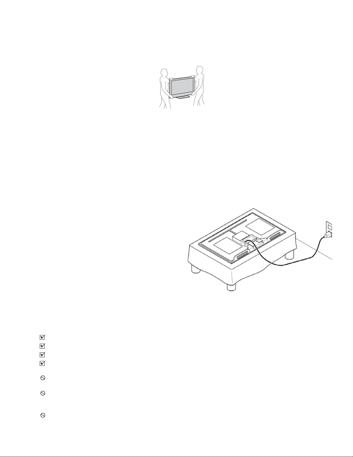
SETTING UP AND CARRYING THE TV
• Disconnect all cables when carrying the TV.
• Carry the TV with the adequate number of people; larger size TVs require two or more people.
• Correct hand placement while carrying the TV is very important for safety and to avoid damage.
Chassis: RB2G, HE-L 5
Page 6
SAFETY CHECK-OUT
Trouble Light
Chassis: RB2G, HE-L
After correcting the original service problem, perform the
following safety checks before releasing the set to the
customer:
1. Check the area of your repair for unsoldered or
poorly soldered connections. Check the entire
board surface for solder splashes and bridges.
2. Check the interboard wiring to ensure that no
wires are “pinched” or touching high-wattage
resistors.
3. Check that all control knobs, shields, covers,
ground straps, and mounting hardware have been
replaced. Be absolutely certain that you have
replaced all the insulators.
4. Look for unauthorized replacement parts,
particularly transistors, that were installed during
a previous repair. Point them out to the customer
and recommend their replacement.
5. Look for parts which, though functioning, show
obvious signs of deterioration. Point them out to
the customer and recommend their replacement.
6. Check the line cords for cracks and abrasion.
Recommend the replacement of any such line
cord to the customer.
7. Check the antenna terminals, metal trim,
“metallized” knobs, screws, and all other exposed
metal parts for AC leakage. Check leakage as
described in “Leakage Test”.
LEAKAGE TEST
The AC leakage from any exposed metal part to earth
ground and from all exposed metal parts to any exposed
metal part having a return to chassis, must not exceed
0.5 mA (500 microamperes). Leakage current can be
measured by any one of three methods.
1. A commercial leakage tester. Follow the
manufacturers’ instructions provided with the
tester.
2. A battery-operated AC milliammeter.
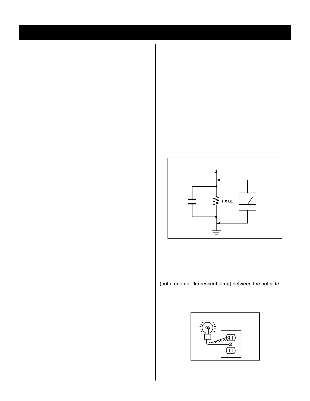
3. Measuring the voltage drop across a resistor
by means of a VOM or battery-operated AC
voltmeter. The “limit” indication is 0.75 V, so
analog meters must have an accurate low
voltage scale. Nearly all battery-operated digital
multimeters that have a 2 VAC range are suitable.
(see Figure A)
To Exposed Metal
Parts on Set
AC
0.15 µF
Voltmeter
(0.75V)
Chassis: RB2G, HE-L 6
Earth Ground
Figure A. Use an AC voltmeter to check AC leakage.
HOW TO FIND A GOOD EARTH GROUND
The cover-plate retaining screw on most AC outlet boxes
is at earth ground. Verify the AC outlet box retaining screw
ground by connecting a 60W to 100W incandescent
of the receptacle and the retaining screw. Try both slots,
if necessary, to locate the hot side on the line; the lamp
should light at normal brilliance if the screw is at ground
potential. (see Figure B)
AC Outlet Box
Figure B. Checking for earth ground.
Page 7
Chassis: RB2G, HE-L
Th
e circuit boards used in these models have been processed using
Due
This
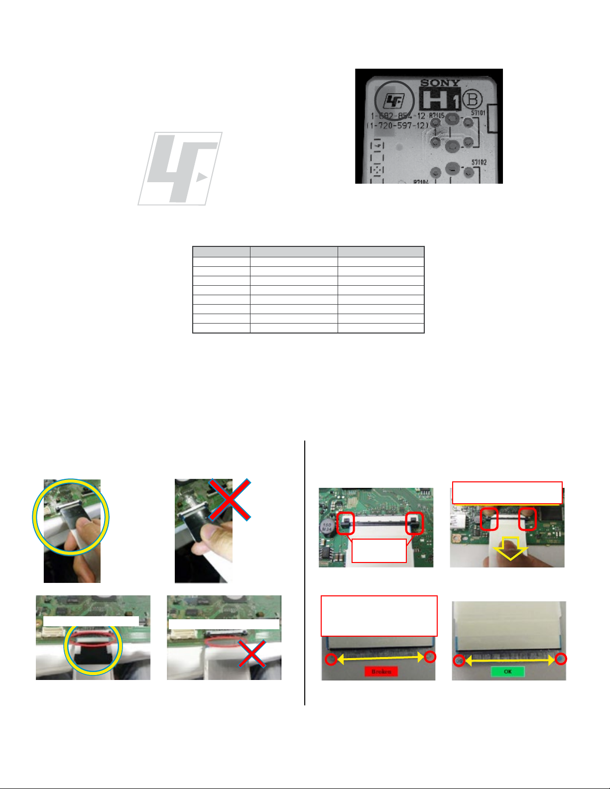
Lead Free Solder. The boards are identified by the LF logo located
close to the board designation e.g. H1 etc [ see example ]. The
servicing of these boards requires special precautions to be taken as
outlined below.
example
It is strongly recommended to use Lead Free Solder material in order to guarantee optimal quality of new solder joints.
Lead Free Solder is available under the following part numbers :
rebmuntraP retemaiD skrameR
91-500-046- m7 m3. g0 K52.0
02-500-046- m7 m4. g0 K05.0
12-500-046- m7 m5. g0 K05.0
22-500-046- m7 m6. g0 K52.0
32-500-046- m7 m8. g0 K00.1
42-500-046- m7 m0. g1 K00.1
52-500-046- m7 m2. g1 K00.1
62-500-046- m7 m6. g1 K00.1
to the higher melting point of Lead Free Solder the soldering iron tip temperature needs to be set to 370 degrees celsius.
requires soldering equipment capable of accurate temperature control coupled with a good heat recovery characteristics.
HANDLING THE FLEXIBLE FLAT CABLE (FFC)
When you connect / disconnect the FFC, please hold
Reinforcement Plastic and FFC Cable as shown below:
GOOD
Connect LVDS
holding both the
FFC Cable and
reinforcement
plastic.
GND Shield must be facing up
Terminal Side must be facing down
GOOD
DO NOT pull
or insert
LVDS holding
only from the
reinforcement
plastic.
NOT
To avoid any damage to the Connector and/or the FFC Cable
follow the steps show:
Press and Hold both Release Buttons at
the sametime to Pull out/ connect FFC
Release Buttons
from CN8700
If pulled without pressing both Release
Buttons, FFC Connector will break on
CN8700. This will cause 5X Blinking error.
GOOD NOT GOOD
Chassis: RB2G, HE-L 7
Page 8
Chassis: RB2G, HE-L
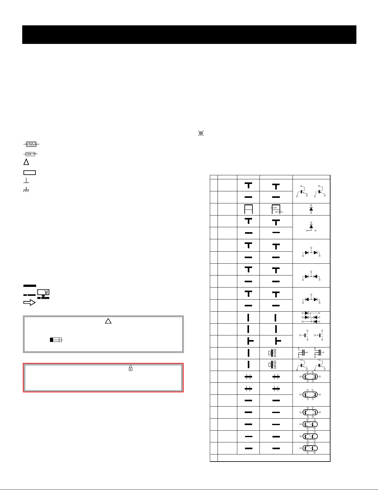
Terminal name of semiconductors in silk screen
SECTION 1: DIAGRAMS
1-1. PRINTED CIRCUIT BOARDS AND SCHEMATIC DIAGRAMS INFORMATION
REFERENCE INFORMATION
All capacitors are in µF unless otherwise noted. pF : µµF 50WV or
less are not indicated except for electrolytics and tantalums.
All electrolytics are in 50V unless otherwise specied.
All resistors are in ohms. kΩ=1000Ω, MΩ=1000kΩ
Indication of resistance, which does not have one for rating
electrical power, is as follows: Pitch : 5mm
Rating electrical power :
1
/4 W in resistance, 1/
W and 1/
10
W in chip resistance.
16
1
/4 W
: nonammable resistor
: fusible resistor
RESISTOR
: RN METAL FILM
: RC SOLID
: FPRD NONFLAMMABLE CARBON
: FUSE NONFLAMMABLE FUSIBLE
: RW NONFLAMMABLE WIREWOUND
: RS NONFLAMMABLE METAL OXIDE
: RB NONFLAMMABLE CEMENT
: ADJUSTMENT RESISTOR
COIL
: LF-8L MICRO INDUCTOR
: internal component
: panel designation and adjustment for repair
: earth ground
printed circuit ( )
Device Printed symbol Terminal name
Transistor
1
*
: earth-chassis
Transistor
2
All variable and adjustable resistors have characteristic curve B, unless
3
Diode
Cathode
otherwise noted.
Readings are taken with a color-bar signal input.
Readings are taken with a 10MΩ digital multimeter.
Voltages are DC with respect to ground unless otherwise noted.
Voltage variations may be noted due to normal production
tolerances.
All voltages are in V.
S : Measurement impossibility.
: B+line.
: B-line. (Actual measured value may be different).
: signal path. (RF)
Circled numbers are waveform references.
The components identied by shading and ! symbol are critical for safety. Replace
only with part number specied.
The symbol indicates a fast-blow fuse and is displayed on the component
side of the board. Replace only with fuse of the same rating as marked.
NOTE: The components identied by a red outline and a mark contain condential
information. Specic instructions must be adhered to whenever these components
are repaired and/or replaced.
See Appendix A: Encryption Key Components in the back of this manual.
Diode
Diode
5
Diode
6
Diode
7
8
Diode
Diode
9
Diode
10
Diode
11
Diode
12
Transistor
13
(FET)
Transistor
14
(FET)
Transistor
15
(FET)
Transistor
16
Transistor
17
Transistor
18
Transistor
19
Transistor
20
Transistor
21
Transistor
22
Transistor
23
Discrete semiconductor
–
(Chip semiconductors that are not actually used are included.)
Anode
Anode
Anode
Anode Cathode
Anode
Anode Anode
Cathode
Cathode
Anode
Anode
Cathode
4
Chassis: RB2G, HE-L 8
CAPACITOR
: TA TANTALUM
: PS STYROL
: PP POLYPROPYLENE
: PT MYLAR
: MPS METALIZED POLYESTER
: MPP METALIZED POLYPROPYLENE
: ALB BIPOLAR
: ALT HIGH TEMPERATURE
: ALR HIGH RIPPLE
Collector
Base
Collector
Base
Cathode
Cathode
Common
Common
Common
Common
Common
Common
Drain
Drain
C2
C1
E1
E2
C2
B1
E2
C2
Emitter
Emitter
(NC)
(NC)
Cathode
Anode
Cathode
Cathode
Cathode
Anode
Anode
Source
Gate
Source
Gate
Source
Drain
Gate
Emitter
Collector
Base
B1 E1
B2 C1E2
B2 E2
B1 C2
B2 E2C1
B1 C2E1
B2 E2C1
B1 C2E1
B1 E1
C1(B2)
(B2)
E1
E2
C2C1
(B2)
E1
B1
C1
Anode
Circuit
D
G
D
S
B1
B1
B1
B1
B1
B1
D
G
S
S
D
G
S
C2
C1
B2
E1
E2
C2
C1
B2
E1
E2
E2
E1
B2
C1
C2
C2C1(B2)
E2
E2
E2E1(B2)
C1
C2
C2E1(B2)
C1
C2
Ver.1.6
G
Page 9
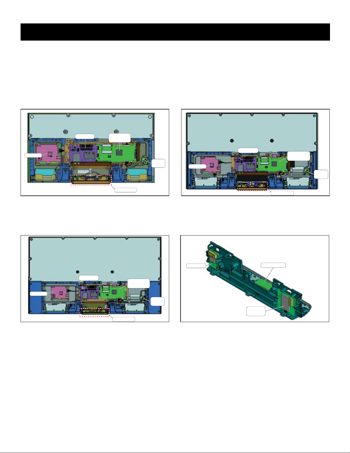
1-2. CIRCUIT BOARDS LOCATION
Chassis: RB2G, HE-L
SECTION 1: DIAGRAMS
LD BOARD
LD BOARD
TUS BOARD
MAIN BOARD
(BAX BOARD)
SMART CORE
SWITCH
UNIT
TUS BOARD
LD BOARD
SMART CORE
Figure 1-2. 42” ModelsFigure 1-1. 32” Models
WIRELESS
LAN CARD
HSC2-S BOARD
TUS BOARD
MAIN BOARD
(BAX BOARD)
SMART CORE
SWITCH
UNIT
BT MODULE
Figure 1-3. 50”/55” Models Figure 1-4. Smart Core
MAIN BOARD
(BAX BOARD)
SWITCH
UNIT
Chassis: RB2G, HE-L 9
Page 10
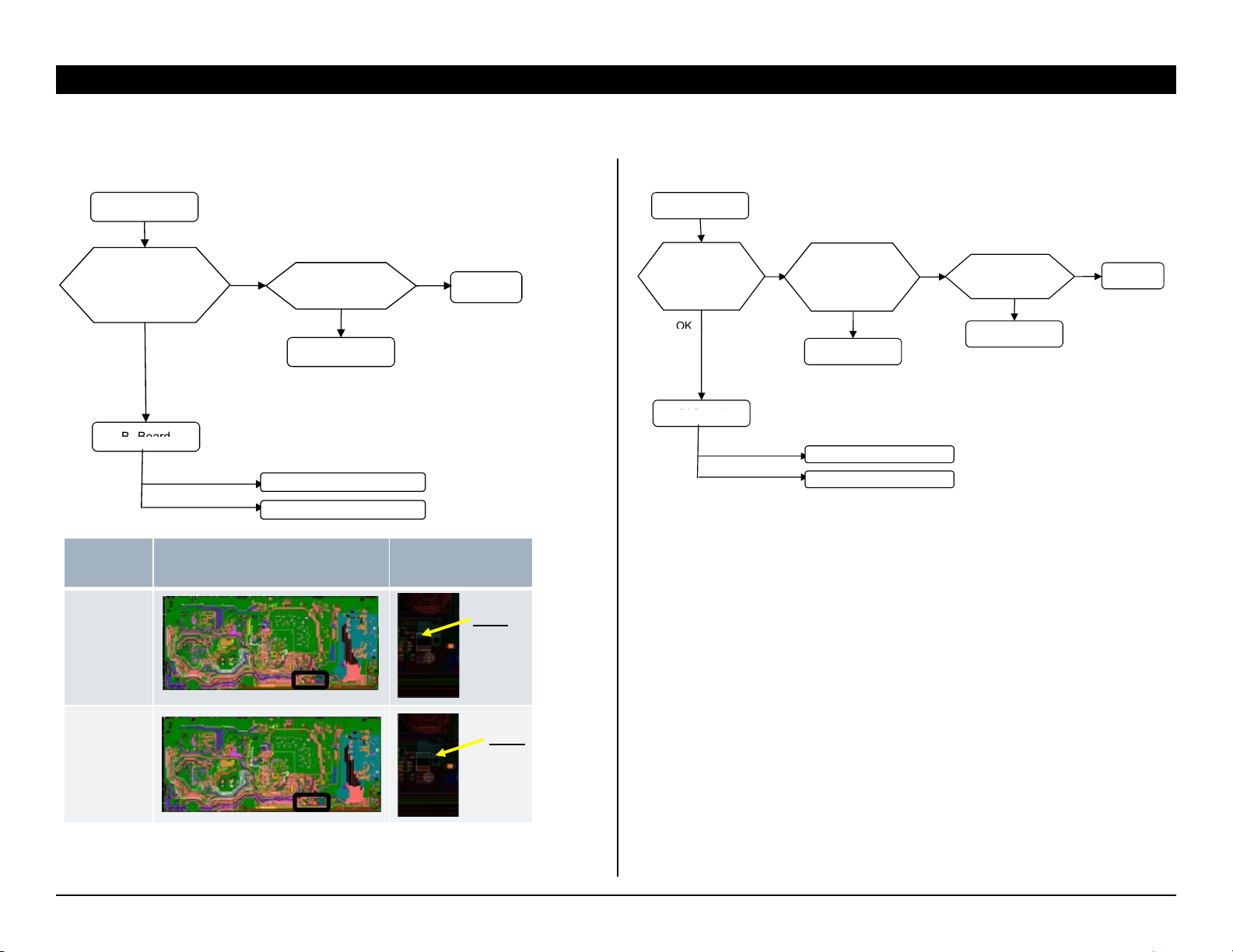
SECTION 2: TROUBLESHOOTING
RB2G CHASSIS
W700B/ W800B
TROUBLESHOOTING
SECTION 2
2-1
. No
Power
No Power
2-1-2. No Power
AC Adaptor
2-1-1. General
NG
NG
Check STBY 3.3V
L9107
Adapter
Replace
Between LD* Board to
B* Board Harness
NG
OK
Replace
LD* Board
OK
Harness
OK
LD* Board
For HT, HM, change LD board.
For HE, change Panel.
B
Board
B*B
oar
d
DC/DC converter check
NO POWER: Ayu2 control
L9107
1-2. No Power
AC Adaptor
OK
B*B
d
[2.1 - NO POWER]
2.1-1 - NO POWER: GENERAL 2.1-2 - NO POWER: AC ADAPTOR
Chassis: RB2G, HE-L
No Power
Check STBY 3.3V
L9107 or C9179
OK
*
Board
Name
BAX
(L9107)
NG
NO POWER: Ayu2 control
Replace
Between G* Board to
B* Board Harness
OK
Harness
DC/DC converter check
NG
Board PWB (B side) Detail
G* Board
No Power
Check STBY 3.3V
L9107
oar
NG
Replace
Between LD* Board to
B* Board Harness
OK
Harness
DC/DC converter check
NO POWER: Ayu2 control
NG
Replace
LD* Board
OK
LD* Board
For HT, HM, change LD board.
For HE, change Panel.
NG
Adapter
BAX
(C9179)
Chassis: RB2G, HE-L 10
C9179
Page 11
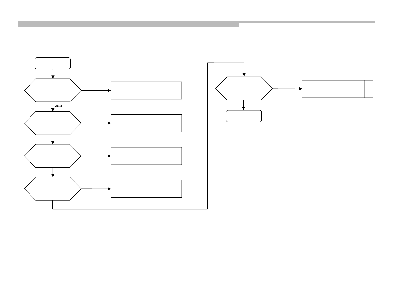
2.1-3 - NO POWER: DC/DC CONVERTER CHECK
RB2G CHASSIS
W700B/ W800B
Troubleshooting
-
-
-
213. No Power
DC/DC converter check
y
yes
y
Chassis: RB2G, HE-L
Check C9007 Voltage.
Is the voltage 1V?
Check C9192 Voltage.
Is the voltage 5V?
Check C9153 Voltage.
Is the voltage 3.3V?
Check C9172 Voltage.
Is the voltage 1.5V?
START
yes
yes
yes
no
no
no
no
Check F9105
Check F9102
Check F9104
Check F9104
Check C9167 is
it 1.18V?
es
END
no
Check F9106
Chassis: RB2G, HE-L 11
Page 12
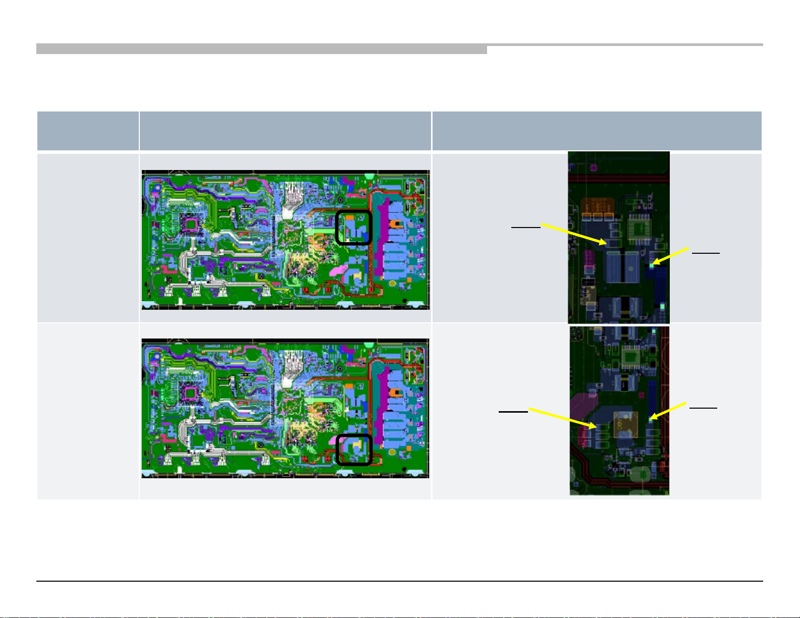
BAX
Board
PWB (A side)
Detail
BAX
BAX
Chassis: RB2G, HE-L
C9007
F9105
Chassis: RB2G, HE-L 12
C9192
F9102
Page 13
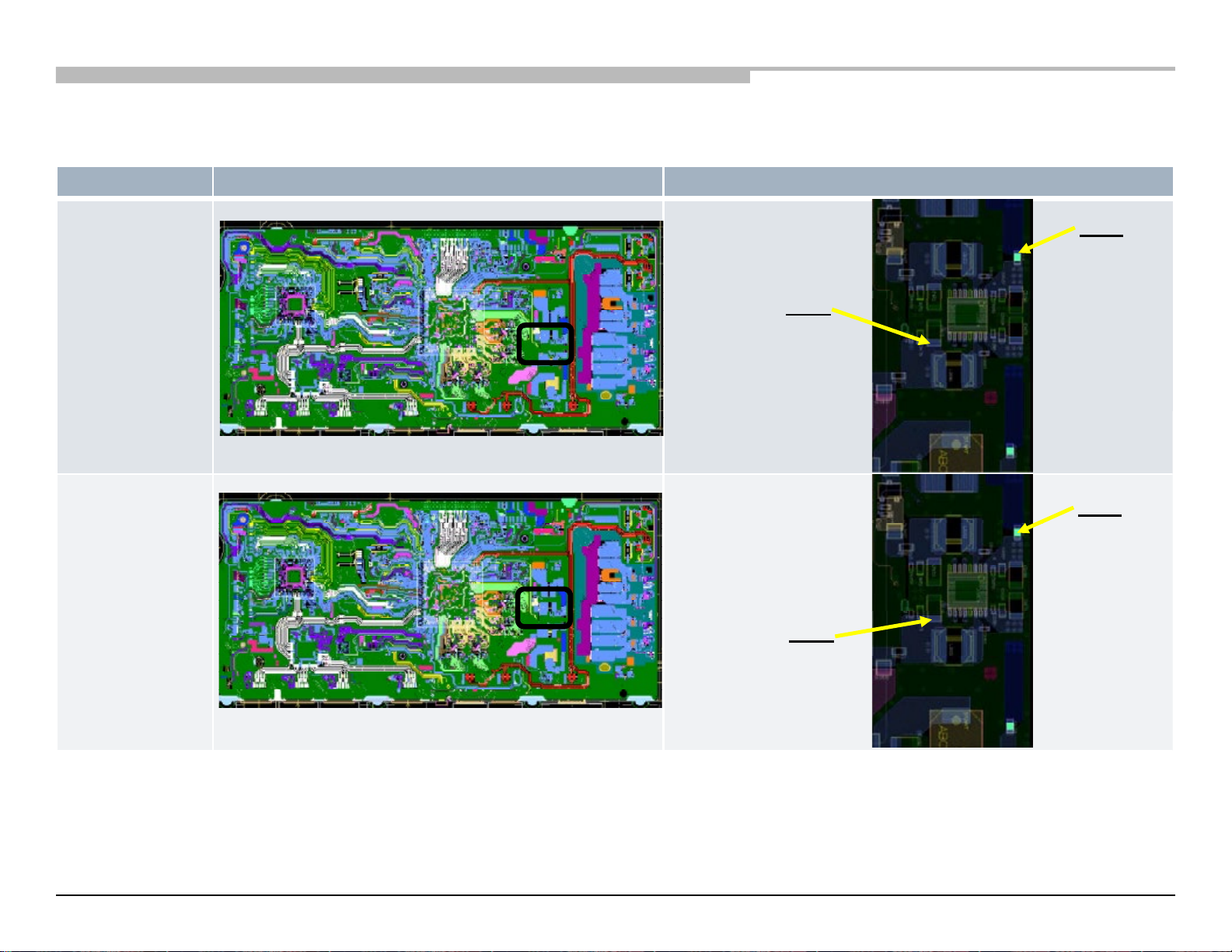
Chassis: RB2G, HE-L
BAX Board PWB (A side) Detail
C9172
BAX
BAX
F9104
C9153
F9104
Chassis: RB2G, HE-L 13
Page 14
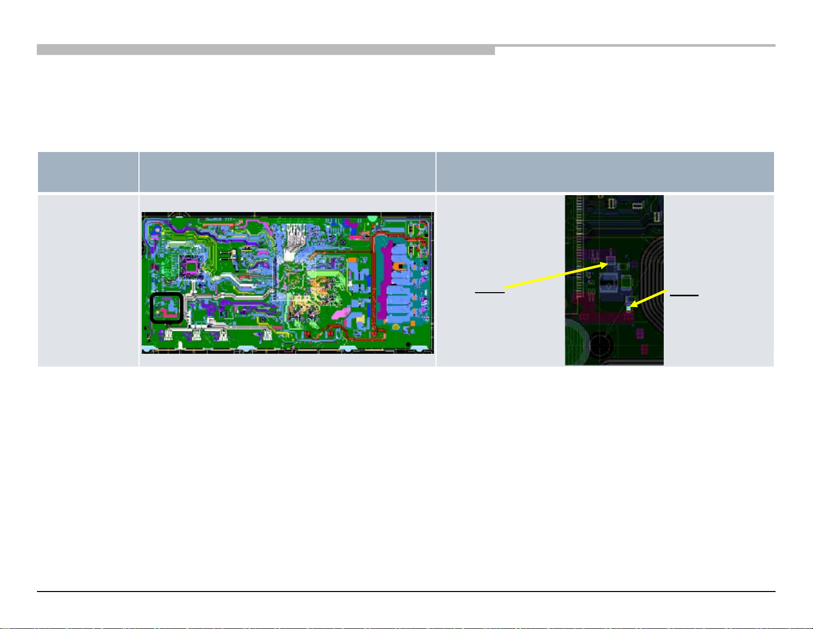
RB2G CHASSIS
W700B/ W800B
Troubleshooting
BAX Board PWB (A side) Detail
BAX
Chassis: RB2G, HE-L
C9167
F9106
Chassis: RB2G, HE-L 14
Page 15
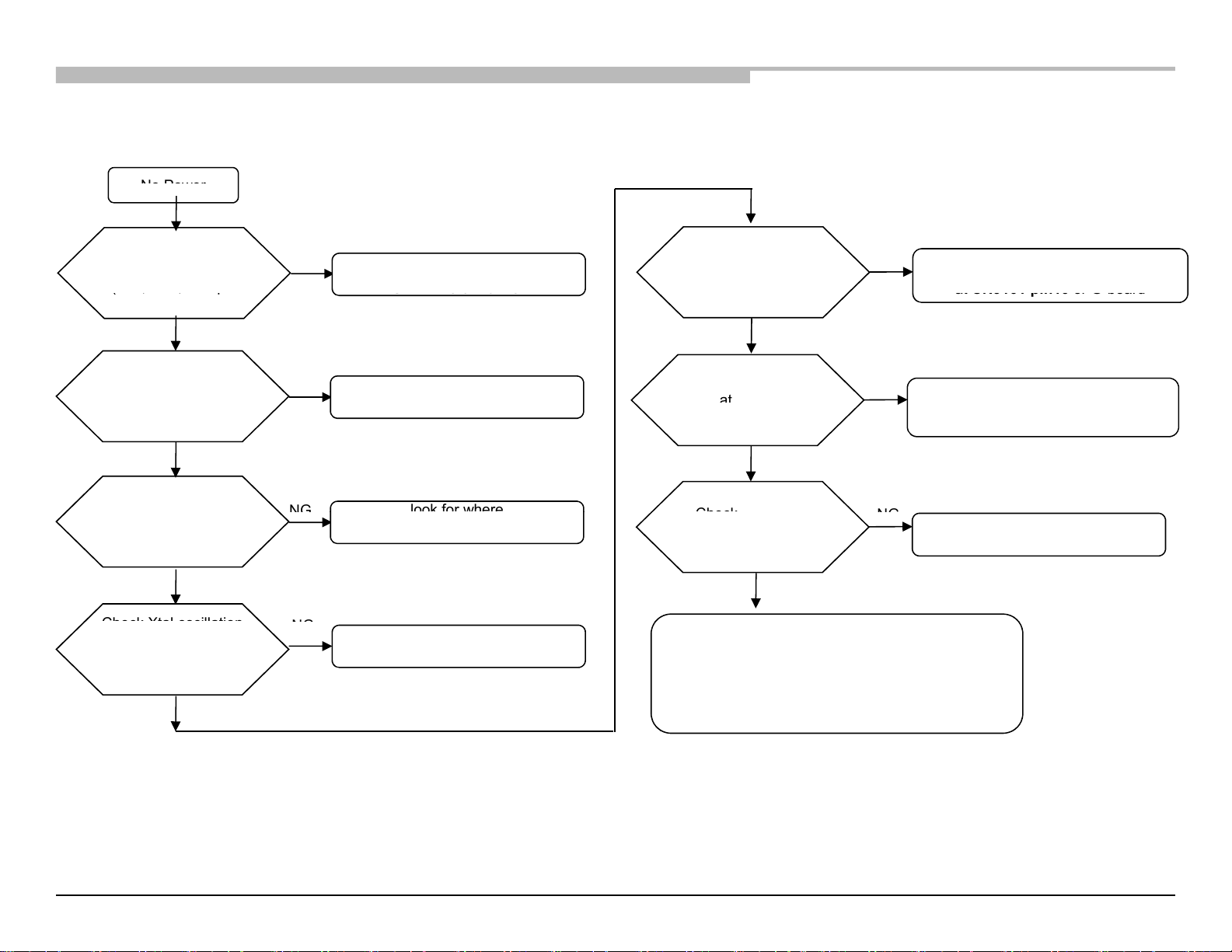
2.1-4 - NO POWER: AYU2 CONTROL
-
4. No Power
:
Ayu2
control
No Power
(
(, , p
at
CN9101 pin10
or G
board
STBY_3.3V
is NG.
at
AYU2
look for where
NG
Check
REG+12V
NG
Check Xtal oscillation
NG
Chassis: RB2G, HE-L
Check STBY_+3.3V
F11, G11, K13 pin
C7348)
OK
Check STBY_+1.8V
at AYU2
(K5, L5, L10, J7 pin
C7349)
OK
Check STBY_+1.0V
at AYU2
(N13, P13 pin C7350)
OK
X7302, 32.768KHz
(A7, B7 pin R7386)
at AYU2
NG
NG
look for where
+
look for where
STBY_+1.8V is NG.
STBY_+1.0V is NG.
Replace X7302 or Ayu2
Check AC_MON
at AYU2
(C6 pin C9131)
OK
Check MAIN_PWR
(A9 pin C9109)
OK
at CN9101 pin23
OK
It might be power supply problem
Please refer "DC/DC converter check" sheet
Or
NG
NG
Look for AC_MON line
Look for MAIN_POWER line
at CN9101 pin21 or replace AYU2
-
G-board
Chassis: RB2G, HE-L 15
OK
Check "STBY LED BLINKING"
Page 16
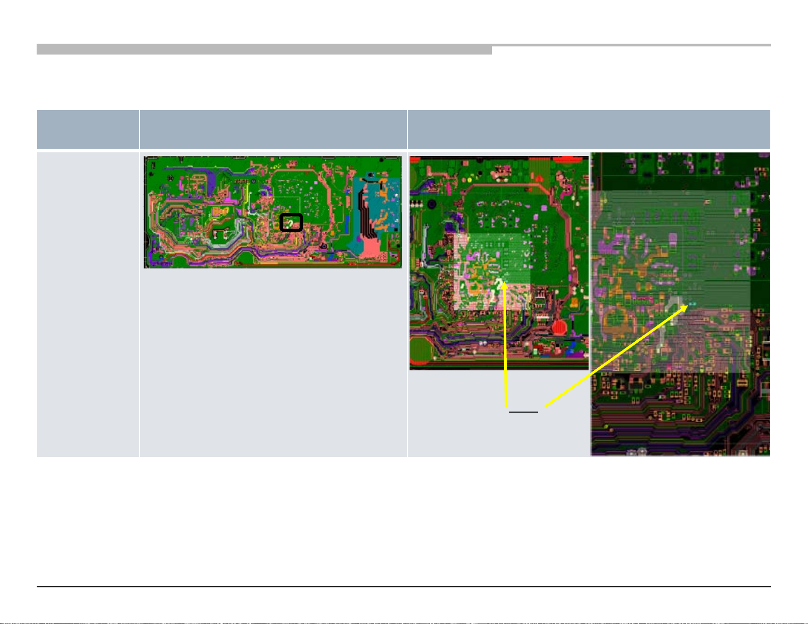
Board
Name
Board
PWB (B side)
Detail
BAX
(C7348)
Chassis: RB2G, HE-L
Chassis: RB2G, HE-L 16
C7348
Page 17
Chassis: RB2G, HE-L
Board
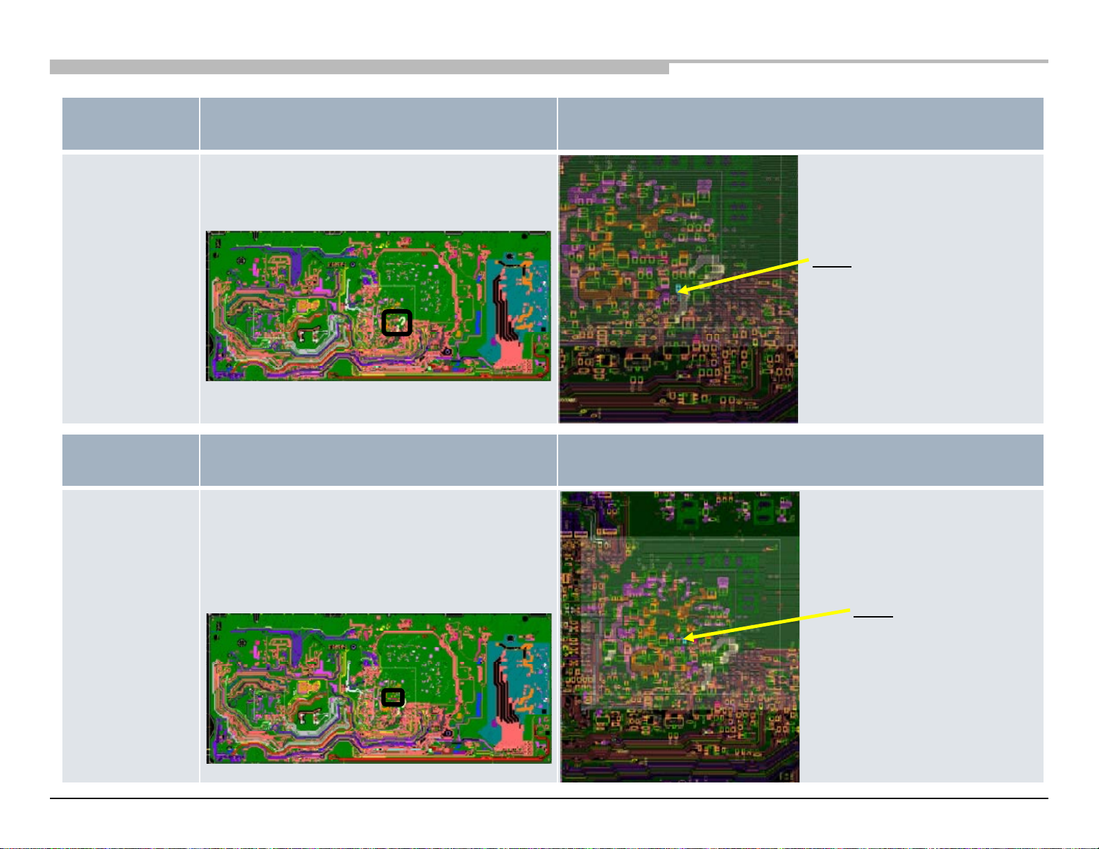
Name
Board PWB (B side) Detail
BAX
(C7349)
C7349
Name
Board
Name
BAX
(C7349)
Board
BAX
(C7350)
Board PWB (B side) Detail
C7349
Board PWB (B side) Detail
C7350
Chassis: RB2G, HE-L 17
Page 18
Chassis: RB2G, HE-L
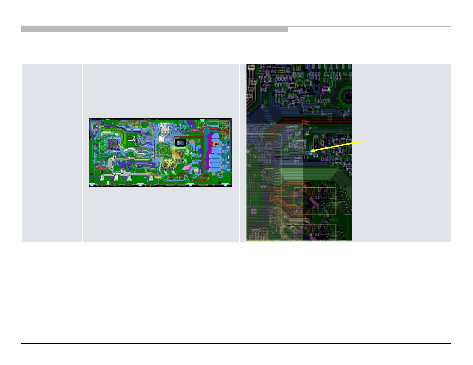
Board
Name
Board PWB (A side) Detail
BAX
(R7386)
R7386
Chassis: RB2G, HE-L 18
Page 19
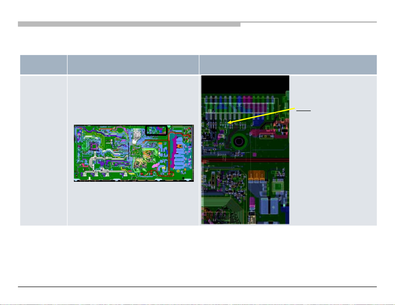
Chassis: RB2G, HE-L
Board
Name
BAX
(C9131)
Board PWB (A side) Detail
C9131
Chassis: RB2G, HE-L 19
Page 20
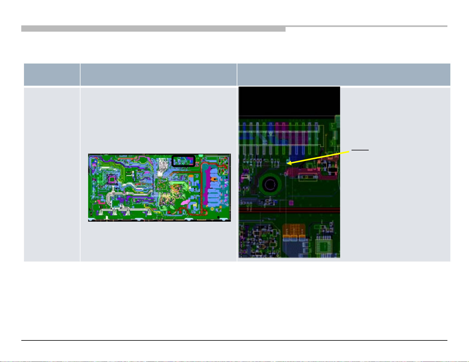
Chassis: RB2G, HE-L
Board
Name
Board PWB (A side) Detail
BAX
(C9109)
C9109
Chassis: RB2G, HE-L 20
Page 21
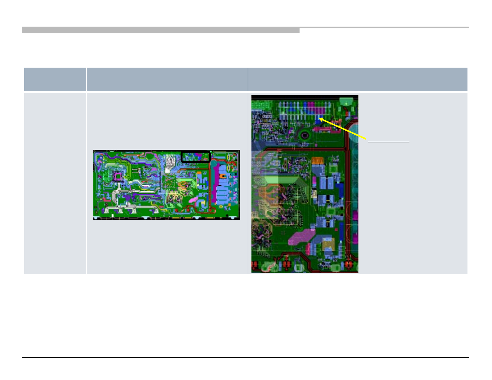
Chassis: RB2G, HE-L
Name
23)
Board
BAX
(CN9101 Pin
Board PWB (A side) Detail
CN9101 Pin 23
Chassis: RB2G, HE-L 21
Page 22
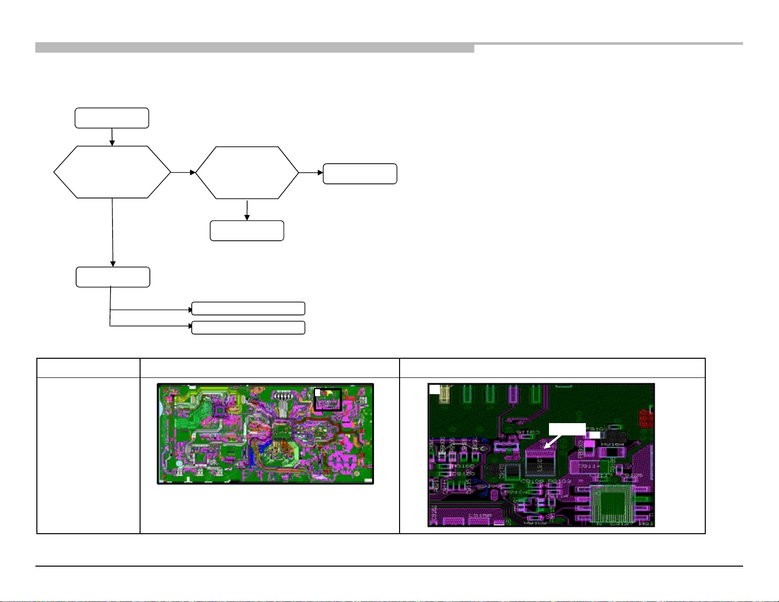
2.1-5 - NO POWER: G BOARD
RB2G CHASSIS
W700B/ W800B
Troubleshooting
*
No Power
2-1-5. No Power
G Board
Check STBY 3.3V
L9107
G* Board
Replace
Between G* Board to
B* Board Harness
NG
NG
Harness
OK
OK
B* Board
DC/DC converter check
NO POWER: Ayu2 control
Board Name
Board PWB (A side) Detail
BAX-
L
1.L9107
L9107
1
1
Chassis: RB2G, HE-L
Chassis: RB2G, HE-L 22
Page 23
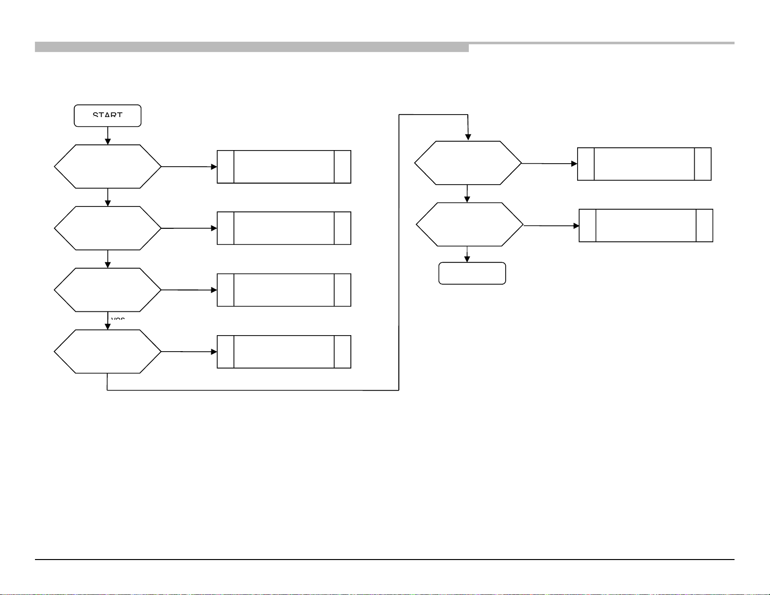
2.1-6 - NO POWER: DC/DC CONVERTER CHECK
RB2G CHASSIS
W700B/ W800B
Troubleshooting
2-1-6. No Power
-
DC/DC converter check
START
yes
Check C9137 Voltage.
Is the voltage 5V?
yes
no
Check F9101
Check C9175 is
it 1.0V?
no
Chassis: RB2G, HE-L
Check F9105
Check C9192 Voltage.
Is the voltage 5V?
yes
Check C9153 Voltage.
Is the voltage 3.3V?
Check C9172 Voltage.
Is the voltage 1.5V?
yes
no
no
no
Check F9102
Check F9104
Check F9104
Check C9167 is
it 1.15V?
yes
END
no
Check F9106
Chassis: RB2G, HE-L 23
Page 24
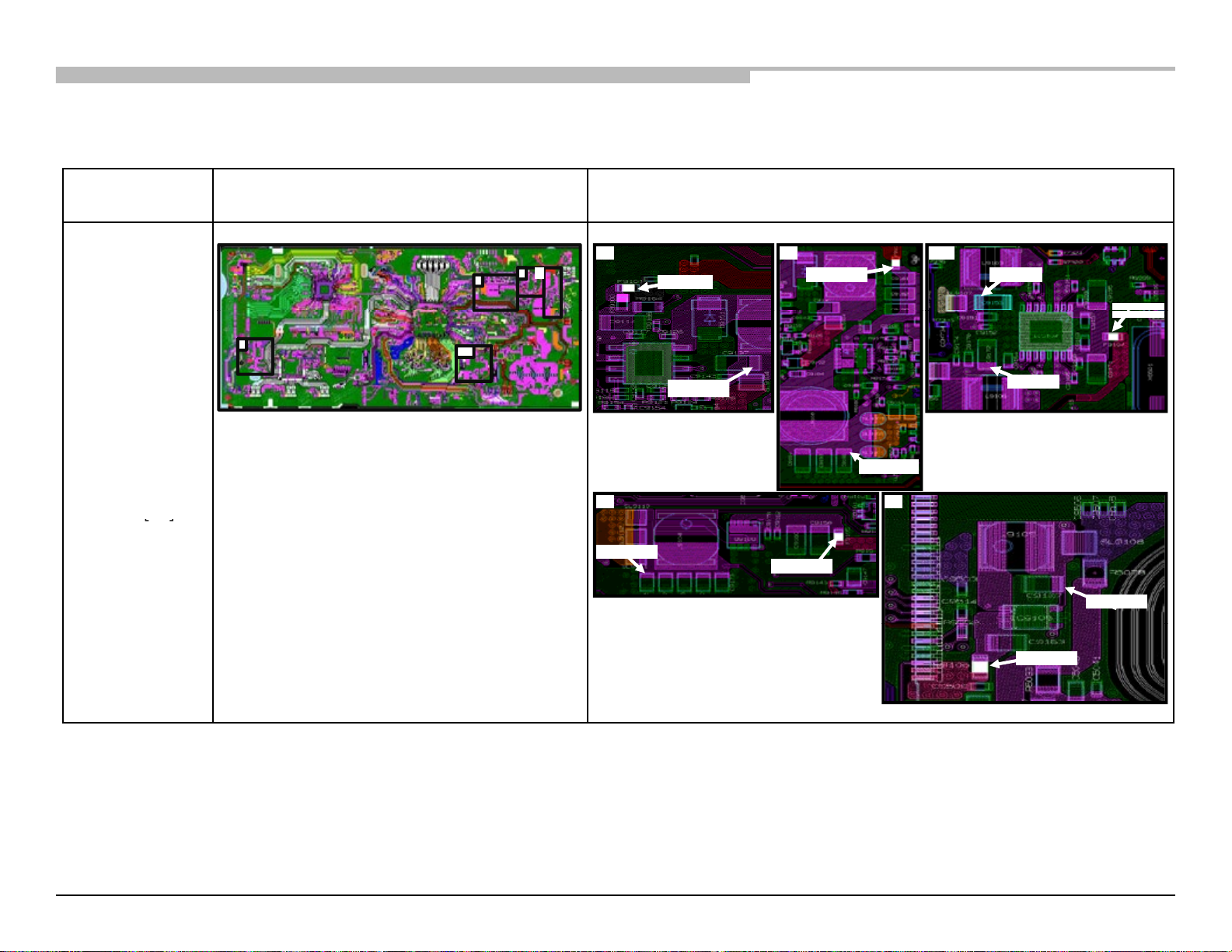
Chassis: RB2G, HE-L
Name
1.C9137 [5V]
F9104
3.C9153 [3.3V]
[1V]
[]
Board
BAX-L
F9101
2.C9192 [5V]
F9102
F9104
4.C9172 [1.5V]
F9104
5.C9175
F9105
6.C9167[1.15V]
F9106
Board PWB (A side) Detail
1 2
1 2
5
6
3,4
F910
1
F9102
C9137
C9192
5 6
C9175
F9105
3, 4
C9153
C9172
C9175
Chassis: RB2G, HE-L 24
F9106
Page 25
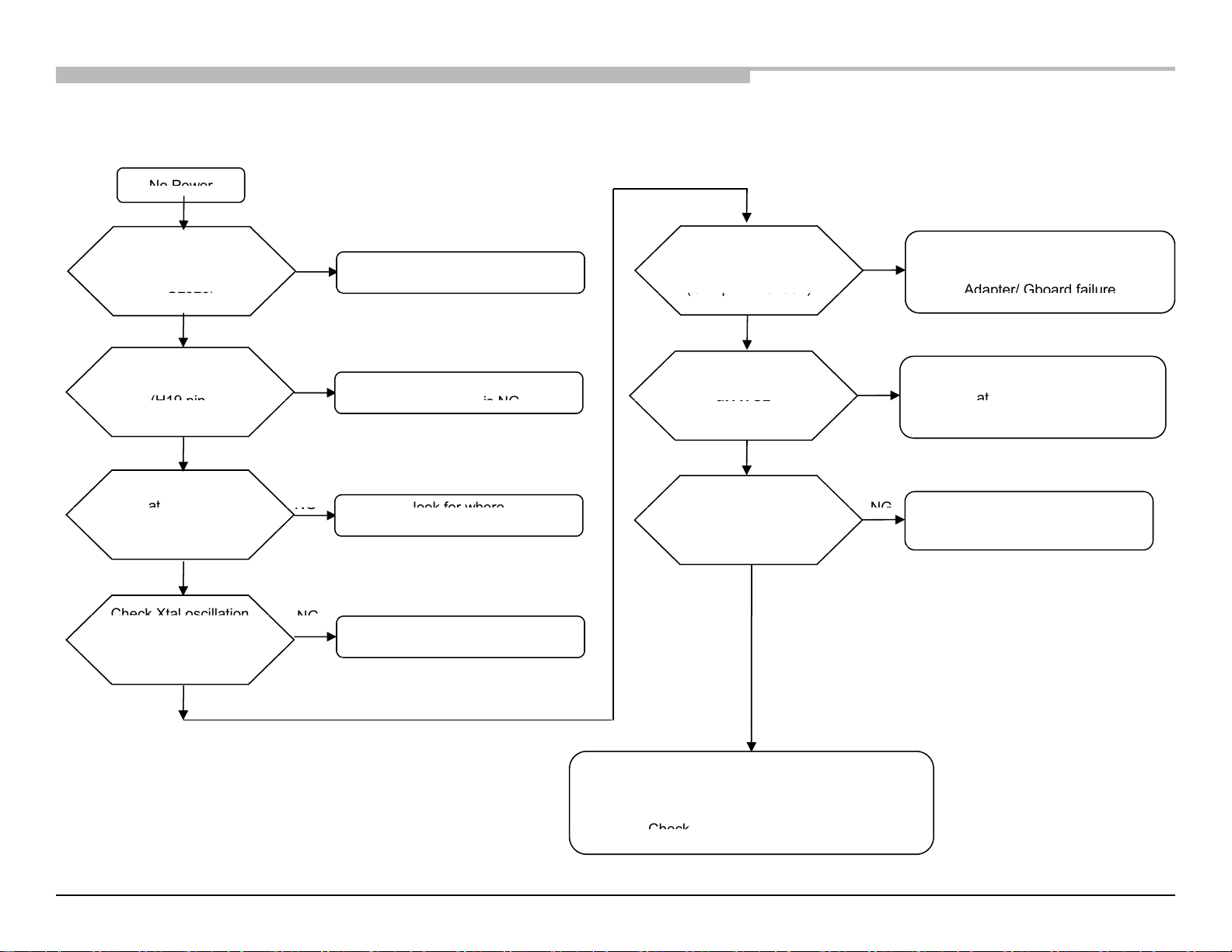
2.1-7 - NO POWER: AYU2L CONTROL
. No
Power
:
Ayu2L
control
No Power
C7376
)
Adapter/
Gboard
failure
(C11 pin
C7334
)
at
CN9101
pin11
at
AYU2
(H19 pin
STBY_+
1.8V
is NG
at
AYU2L
look for where
Adapter/
NG
NG
Check Xtal oscillation
NG
Check
STBY LED BLINKING
Chassis: RB2G, HE-L
Check STBY_+3.3V
(H15, H16, H17 pin
Check STBY_+1.8V
Check STBY_+1.0V
(J15, J16, J17 pin
at AYU2L
OK
at AYU2L
C7374)
OK
C7380)
OK
NG
NG
look for where
STBY_+3.3V is NG.
look for where
STBY_+1.0V is NG.
Check AC_MON
at AYU2
OK
Check MAIN_PWR
.
Check +19.5V(Adapter)
(C13 pin C7315)
OK
Or +12V(G-Board)
at CN9101 pin21
NG
NG
Look for AC_MON line
at CN9101 pin12/C9131 or
Look for MAIN_POWER line
or replace AYU2
G-board
X7301, 32.768kHz
Chassis: RB2G, HE-L 25
(A23, B23 pin
R7398)
OK
Replace X7301 or Ayu2L
OK
It might be power supply problem
Please refer "DC/DC converter check" sheet
Or
"
"
Page 26
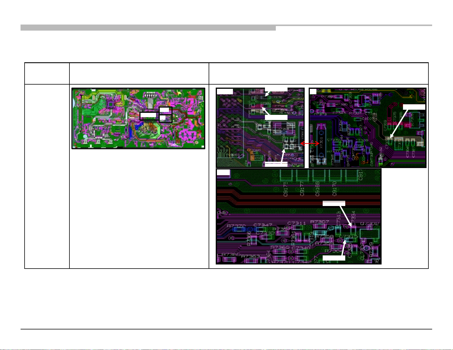
Chassis: RB2G, HE-L
L
C7376
Y
5. C7334
R7396
C7334
Board
Name
BAX-
1. C7376
2. C7374
3. C7380
4. R7396
6. C7315
Board PWB ( A side ) Detail
1, 3, 4
5,6
2
1, 3, 4
C7380
U2L
A
5, 6
2
X7301
C7374
Chassis: RB2G, HE-L 26
C7315
Page 27
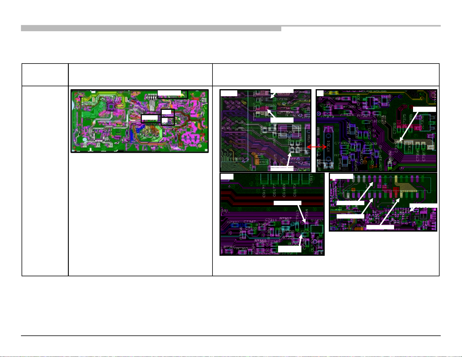
Chassis: RB2G, HE-L
L
C7376
Y
5. C7334
R7396
C9131
Board
Name
BAX-
1. C7376
2. C7374
3. C7380
4. R7396
6. C7315
7. CN9101
Board PWB ( A side ) Detail
1, 3, 4
7. CN9101
5,6
2
1, 3, 4
5, 6
2
C7380
U2L
A
X7301
7. CN9101
C7334
C7374
Pin12
Pin11
Pin21
Chassis: RB2G, HE-L 27
C7315
Page 28
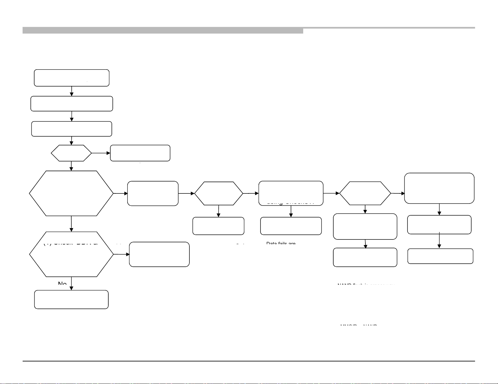
2.1-8 - NO POWER: AYU2/AYU2L FAILURE
RB2G CHASSIS
W700B/ W800B
Troubleshooting
2-1-8. No Power
–
AYU2/AYU2L failure
A
YU2/L Fail Suspected
p
eMMC / RawNAND erase
Product SW rewrite
Recover?
Product SW
writin
g
issue
Yes
Find Some
Error message
AYU2/L LOG is
displayed
Yes
No
Yes
Check
eMMC / RawNAND
Check DDR
using CheckSW
Find Some
Error message
No
g
Check error message
It is unacceptable
error?
eMMC/ RawNAND
data fail
No
Store SW log,
Check SW
behaviors.
No
using CheckSW
No
DDR device fail
Yes
From the error
Erase & Replace
eMMC/ RawNAND
Yes
(1) Check
DDR &
eMMc / RawNAND
interface OK?
Replace
AYU2/L or Board
Y
es
Data fails are
especially in
environment area.
If this Area has broken,
check soft cannot run
In this case, corrupted
data are written to eMMC/
Erase
eMMC/ RawNAND
message, we can find
which device has
failure.
Move to device
analysis phase.
Product SW write
If still NG after SW rewrite,
please go to (1) Check
MMC/RawNAND interface
Replace Board
No
NAND flash in proper way
.
So, we have to check the
logs of exception or errors.
Erase eMMC/ RawNAND
is a last option. If still NG
after erase, please replace
e
MMC
/
RawNAND
Chassis: RB2G, HE-L
Chassis: RB2G, HE-L 28
Page 29
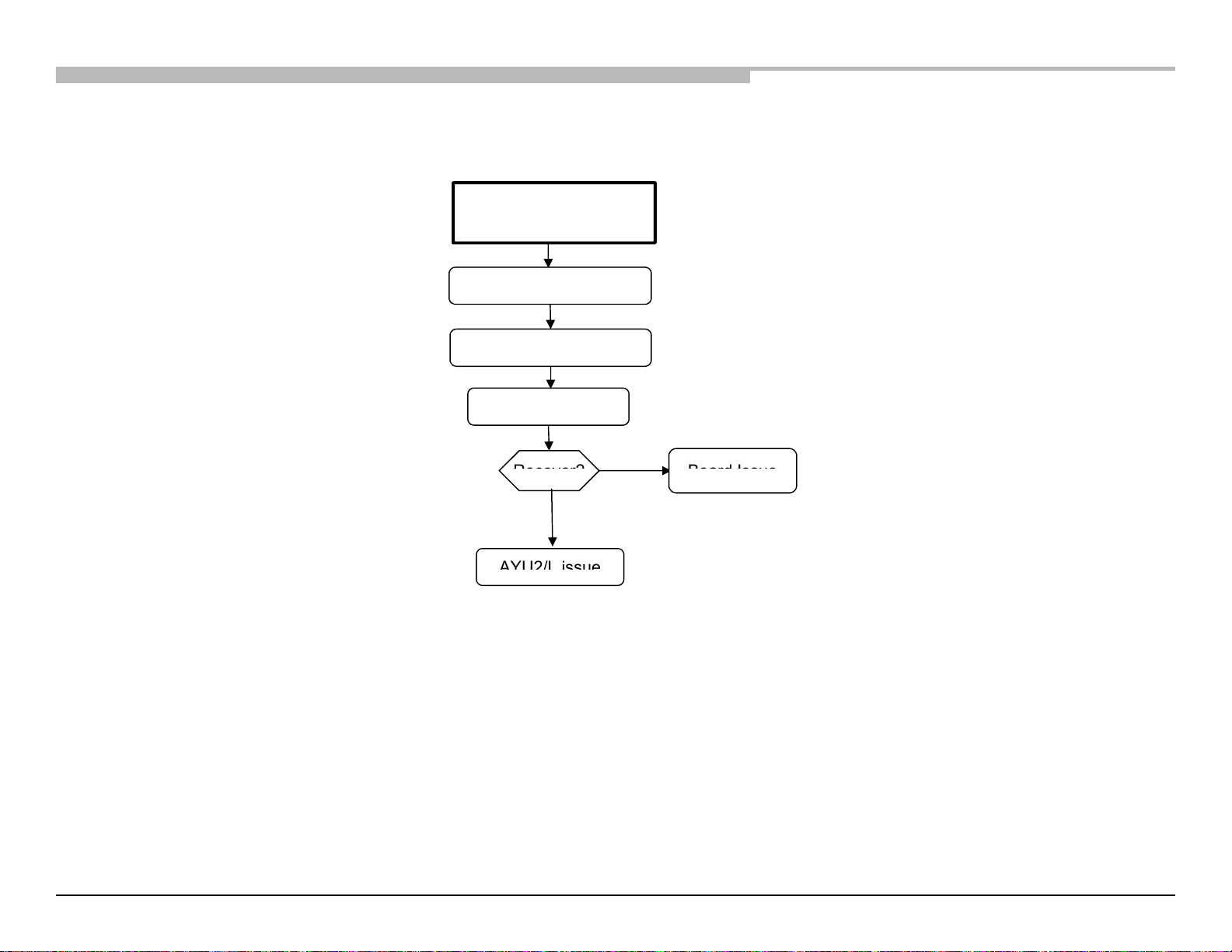
2.1-9 - NO POWER: AYU2/ AYU2L REPLACEMENT
RB2G CHASSIS
W700B/ W800B
Troubleshooting
2-1-9. No Power
–
AYU2/ AYU2L replacement
Recover?
Board Issue
AYU2/L
issue
AYU2/L
replacement flow
Chassis: RB2G, HE-L
eMMC / RawNAND erase
AYU2/L replacement
Product SW write
No
Yes
Data on eMMC/NAND
need to be erase first
before changing AYU2/L.
Chassis: RB2G, HE-L 29
Page 30
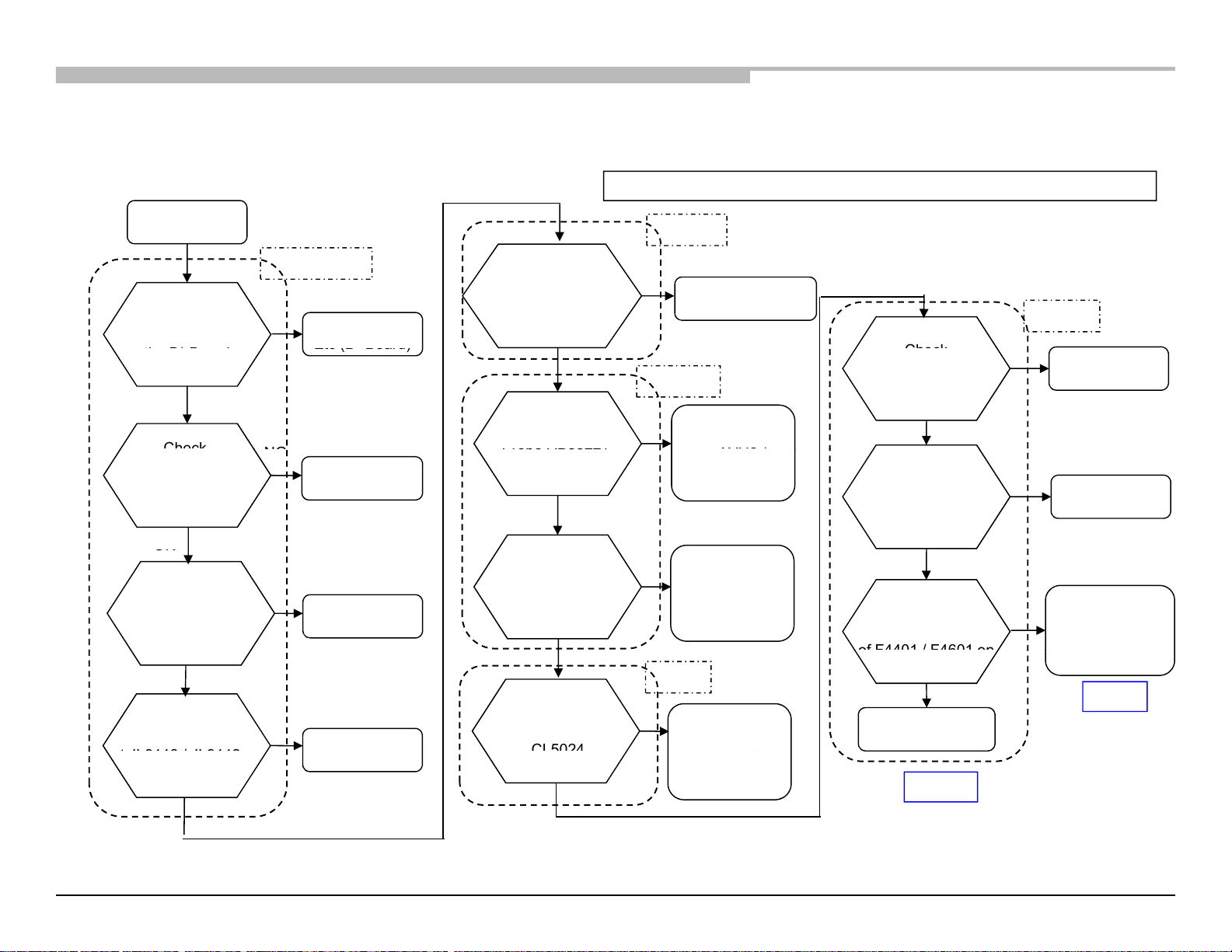
2.2-1 - LED BLINKING: 3X DC ALERT & COMMUNICATION ERROR
RB2G CHASSIS
W700B/ W800B
Troubleshooting
TUNER
3-time blinking
2-2-1. 3x (DC Alert & Communication Error)
Note: For location details, refer to troubleshooting Reference for parts location.
2-2
.
Led Blinking
AUDIO
I2C bus dumping or
AYU2 / AYU2L
NG
Check D+1.0V at
JL9003 / JL9127 on
F9105,IC9103,
*
DC_ALERT
NG
DMD_TU_I2C
or I2CB bus check:
Probe CL2101, CL2102 /
CL2318, CL2101 on
TU* Board
Speaker
Check
Speaker Impedance
at SP Connector
NG
OK
Brownie
the B* B
oar
d
Etc
(B Board)
OK
SPIC check
OK
SPI dumping
resistor
Check
Audio +12.5V
at pin 18/20 of CN9101
on the B* Board
(except Adapter model)
G* Board
NG
OK
Check
+3.3V_MAIN_1
at JL9117 on
the B* Board
F9104,IC9104,
etc (B* Board)
NG
Probe RB8522 /
RB8517
or
AYU2 /
AYU2L
Check
+12.5V / +19.5V
at Power Amp side
F4401 / F4601,
IC4901 / IC4601
,etc
OK
NG
I2C_CCP check
R8502 and R8506 /
R8546 and R8547
I2C_CCP
Pull Up
OK
Check
+1.8V_MAIN on
Pin 2 of IC9201
IC9201,etc
(B* Board)
NG
of F4401 / F4601 on
the B* Board
(B* Board)
IC4901 / IC4601,etc
(B* Board)
OK
#2
I2CA bus check:
Probe CL5023,
I2CA bus
dum
ping
NG
HDMI
OK
NG
Check
+5.0V_MAIN
OK
IC9102 / IC9101
#3
CL5024
pg
resistor
or AYU2
OK
at
JL9113 / JL9112
on
the B* Board
,etc (B* Board)
Chassis: RB2G, HE-L
Chassis: RB2G, HE-L 30
Page 31
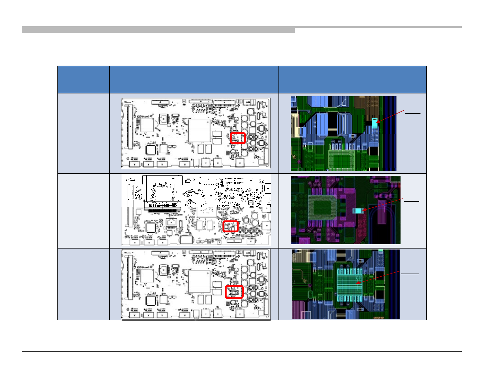
RB2G CHASSIS
W700B/ W800B
Troubleshooting
Board
Name
BAX
(F9104)
BAXL
(F9104)
Chassis: RB2G, HE-L
Board PWB (A side) Detail
F9104
F9104
BAX
(IC9104)
Chassis: RB2G, HE-L 31
IC9104
Page 32
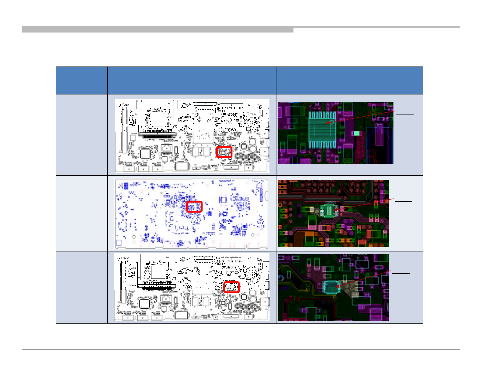
RB2G CHASSIS
W700B/ W800B
Troubleshooting
Board
Name
BAXL
(IC9104)
Chassis: RB2G, HE-L
Board PWB Detail
IC9104
BAX
(IC9201)
B-Side
IC9201
BAXL
(IC9201)
Chassis: RB2G, HE-L 32
IC9201
Page 33
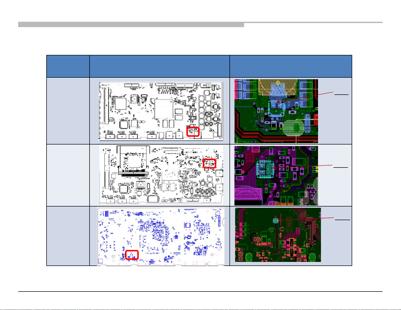
RB2G CHASSIS
W700B/ W800B
Troubleshooting
Board
Name
BAX
(IC9102)
BAXL
(IC9101)
Chassis: RB2G, HE-L
Board PWB (A side) Detail
IC9102
IC9101
BAX
JL9113
(JL9113)
B-Side
Chassis: RB2G, HE-L 33
Page 34
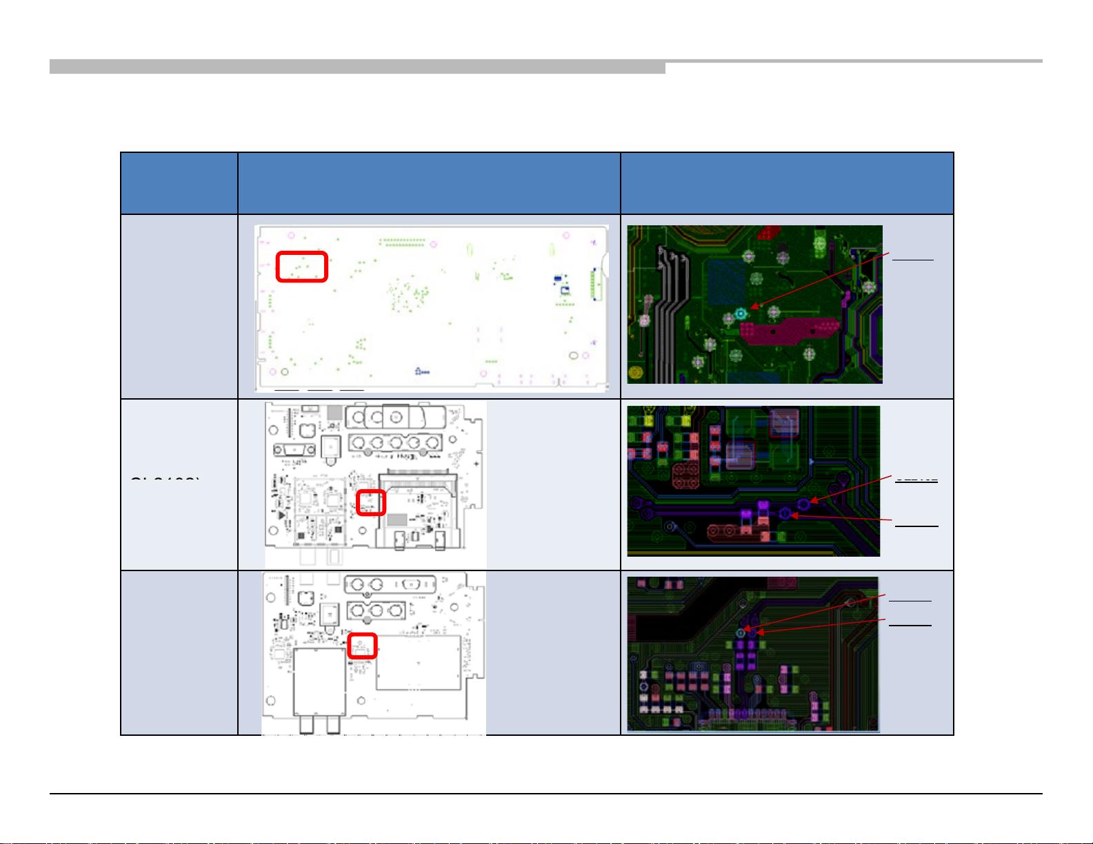
RB2G CHASSIS
W700B/ W800B
Troubleshooting
CL2102)
CL2102
Board
Name
BAXL
(JL9112)
Chassis: RB2G, HE-L
Board PWB Detail
JL9112
B-Side
Chassis: RB2G, HE-L 34
TU-S
(CL2101,
TU-W
(CL2318,
CL2319)
CL2101
CL2318
CL2319
Page 35
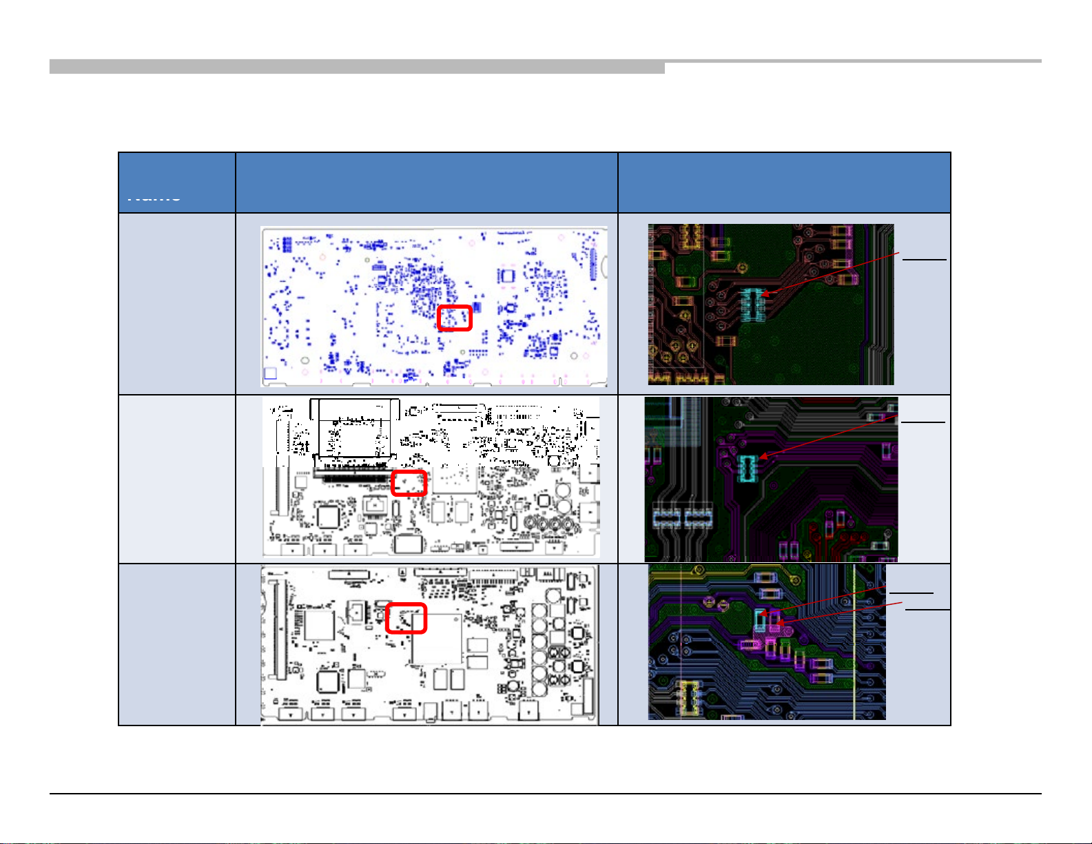
RB2G CHASSIS
W700B/ W800B
Troubleshooting
Troubleshooting Reference
Name
Board
Chassis: RB2G, HE-L
Board PWB (A side) Detail
BAX
(RB8522)
BAXL
(RB8517)
BAX
(R8502,
R8506)
RB8522
B-Side
RB8517
RB8502
RB8506
Chassis: RB2G, HE-L 35
Page 36
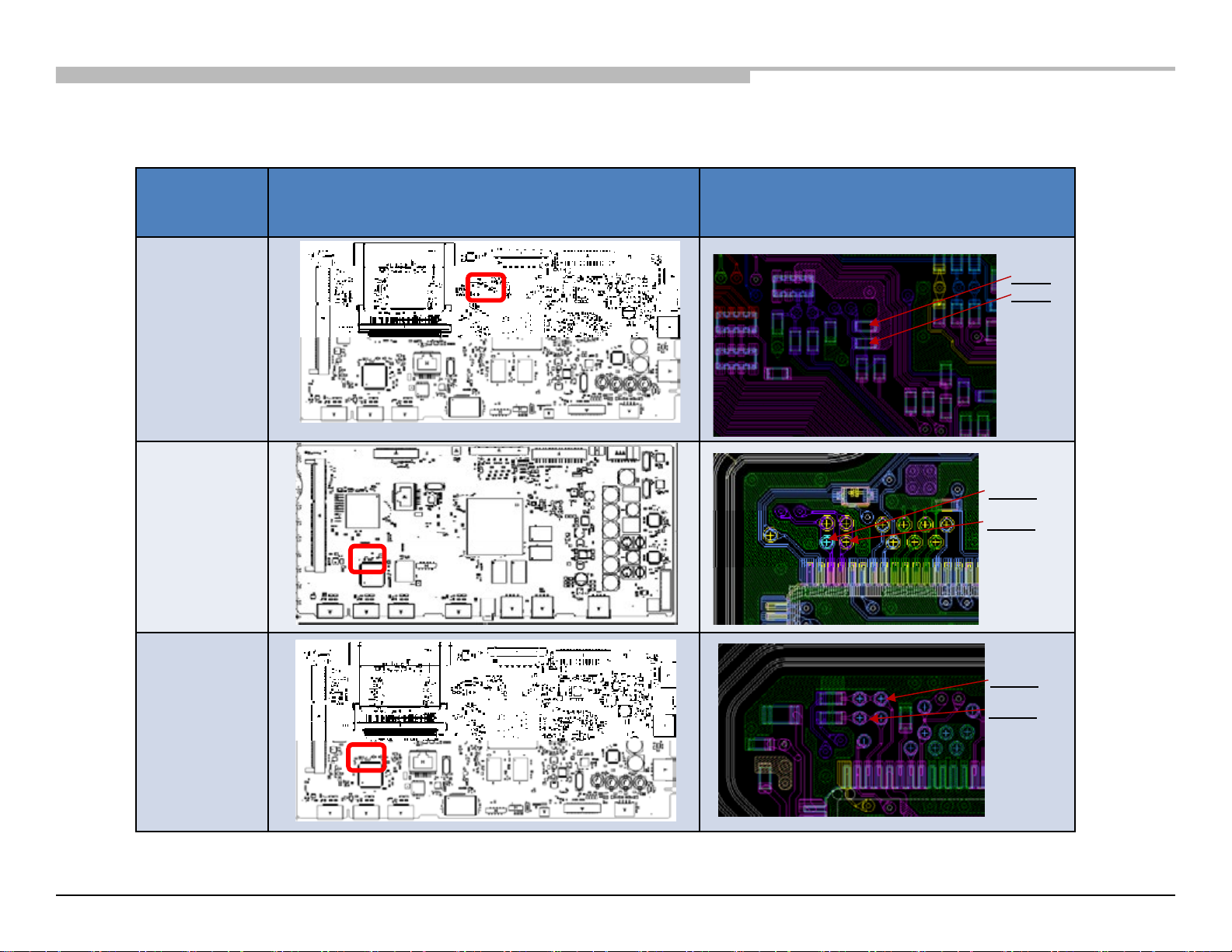
RB2G CHASSIS
W700B/ W800B
Troubleshooting
Board
Name
Chassis: RB2G, HE-L
Board PWB (A side) Detail
BAXL
(R8546,
R8547)
BAX
(CL5023,
CL5024)
BAXL
(CL5023,
CL5024)
R8546
R8547
CL5023
CL5024
CL5024
CL5023
Chassis: RB2G, HE-L 36
Page 37
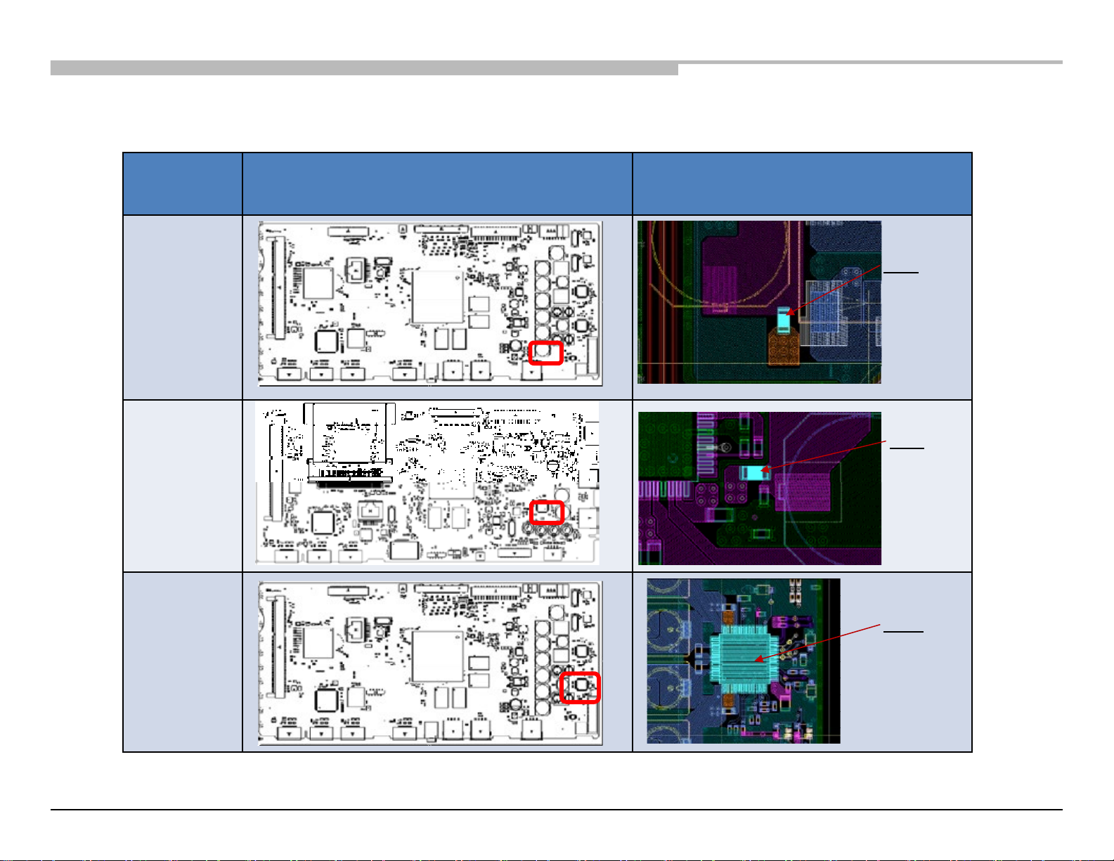
RB2G CHASSIS
W700B/ W800B
Troubleshooting
Board
Name
BAX
(F4401)
BAXL
(F4601)
Chassis: RB2G, HE-L
Board PWB (A side) Detail
F4401
F4601
BAX
(IC4901)
Chassis: RB2G, HE-L 37
IC4901
Page 38
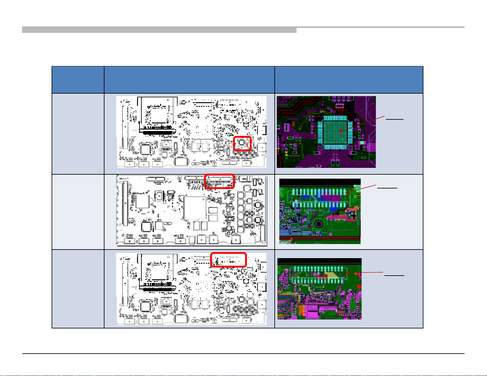
Chassis: RB2G, HE-L
RB2G CHASSIS
W700B/ W800B
Troubleshooting
BAXL
Board
Name
BAXL
(IC4601)
BAX
(CN9101)
Board PWB (A side) Detail
IC4601
CN9101
Chassis: RB2G, HE-L 38
(CN9101)
CN9101
Page 39
Chassis: RB2G, HE-L
RB2G CHASSIS
W700B/ W800B
Troubleshooting
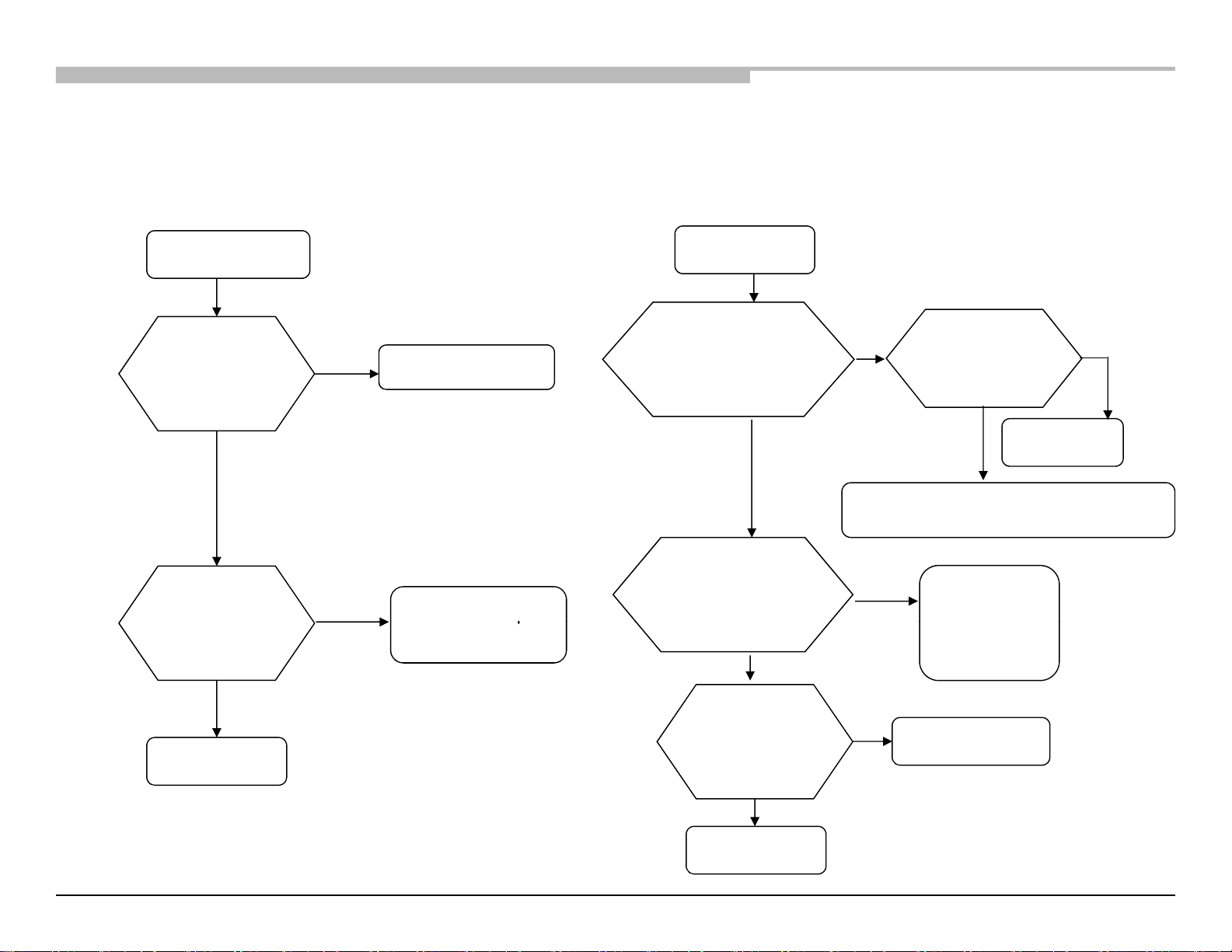
#2
#3
2-2-2. 3x (Audio Error) – BAX-L(HE-L,HM,HE-H)board only
2-2. Led Blinking
NG
p
2.2-2 - LED BLINKING: 3X(AUDIO ERROR) - BAX-L(HE-L,HM,HE-H) BOARD ONLY
#2 #3
F4601,IC4601,etc
(B* Board)
Check 19.5V
(at fuse F4601)
High
enough
Replace F4601
to GND
impedance
Low impedance
IC4601,etc
(B* Board)
Check the IC4601
Out pin 37, 41, 44, 46
Switching 0V to 19V
around 300-400kHz
Yes
No
Check the IC4601
pin 18 (at CL4606)
is HIGH?
Yes
Solder NG
IC4601 or parts around IC4601
No
Chassis: RB2G, HE-L 39
IC4601
burn or broken ?
Yes
Replace IC4601
No
Check broken parts
around IC4601
Check the CN4601
DC level ~9.7V
(at JL4621~JL4624)
Yes
Check the IC4601
I2S line pin
4, 12, 15, 16 (at
CL4601~CL4604)
OK
IC4601 NG
No
L4601-L4604
or C4611-C4614
NG
NG
IC9000 NG
Page 40
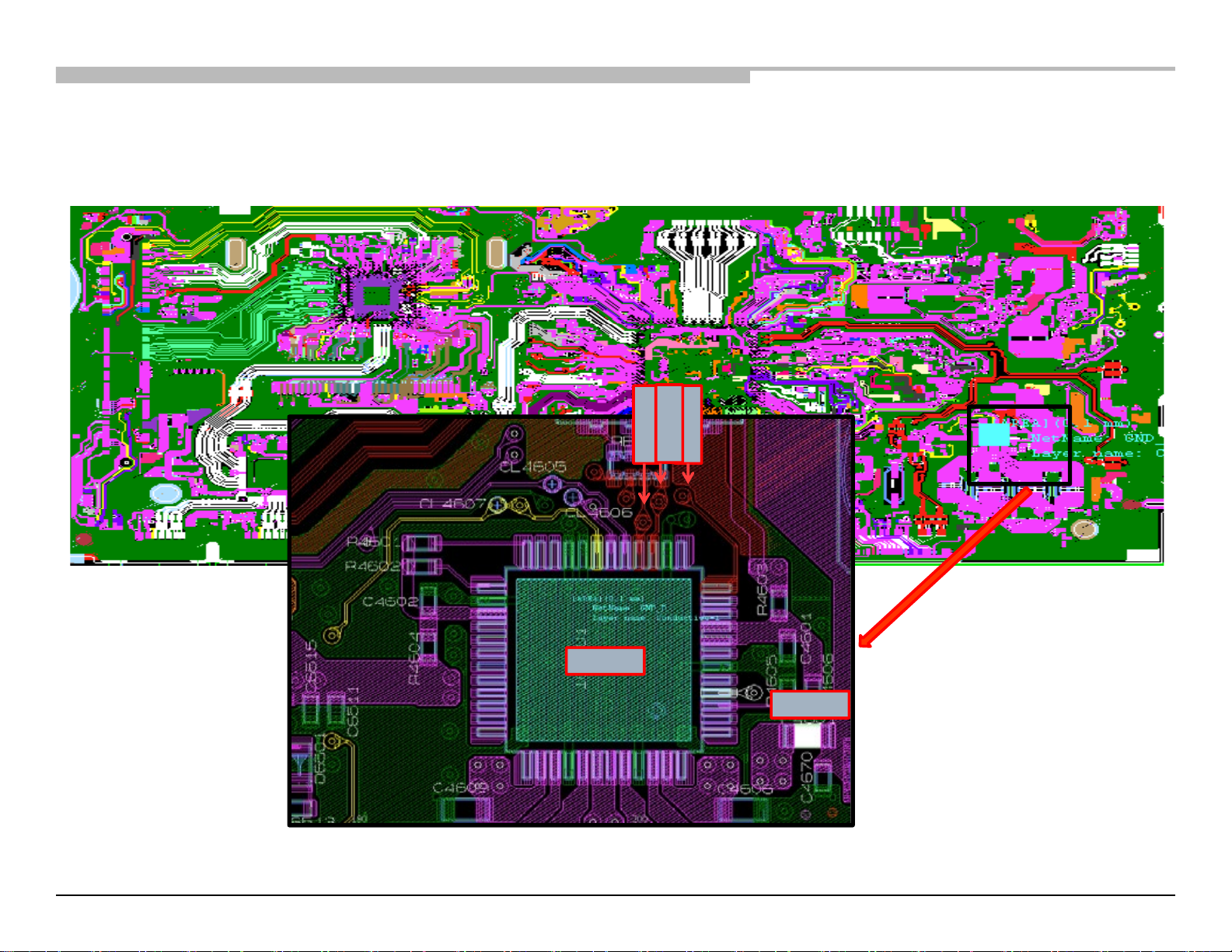
RB2G CHASSIS
W700B/ W800B
Troubleshooting
6
6
6
4
03
CL4
04
02
CL4
CL4
Chassis: RB2G, HE-L
24
25
18
12
13
16
15
IC4601
F4601
36 1
37
Chassis: RB2G, HE-L 40
39
41
44
46
48
Page 41
RB2G CHASSIS
W700B/ W800B
Troubleshooting
Chassis: RB2G, HE-L
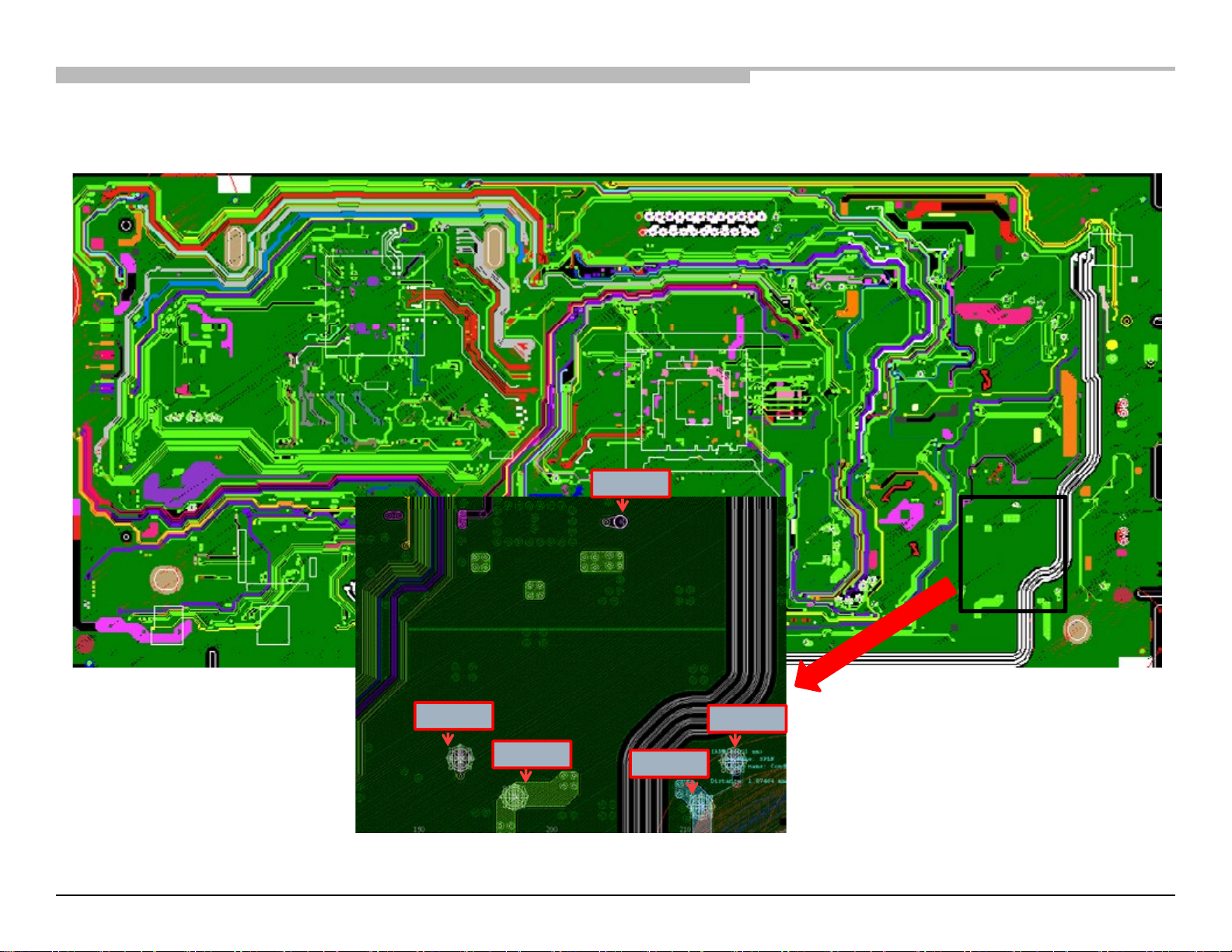
CL4601
JL4624
JL4623
Chassis: RB2G, HE-L 41
JL4622
JL4621
Page 42
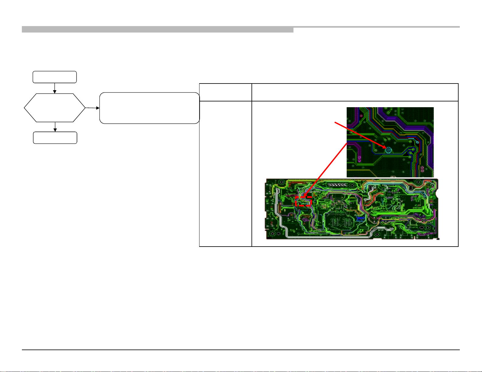
2.2-3 - LED BLINKING: 4X LED VOLTAGE ERROR
RB2G CHASSIS
W700B/ W800B
Troubleshooting
2-2-3. 4x (LED Voltage Error)
2-2. Led Blinking
Chassis: RB2G, HE-L
4-time blinking
Between 0.49V to 1.32V
Check
BACKLIGHT_MON
on the B* Board
B* Board
LED driver
For HT, HM, change LD board.
For HE, change Panel.
Board /Parts Board PWB (BAX-L – B SIDE)
BAXL
BACKLIGHT_MON
= JL9106
BACKLIGHT_MON
= JL9106
Chassis: RB2G, HE-L 42
Page 43
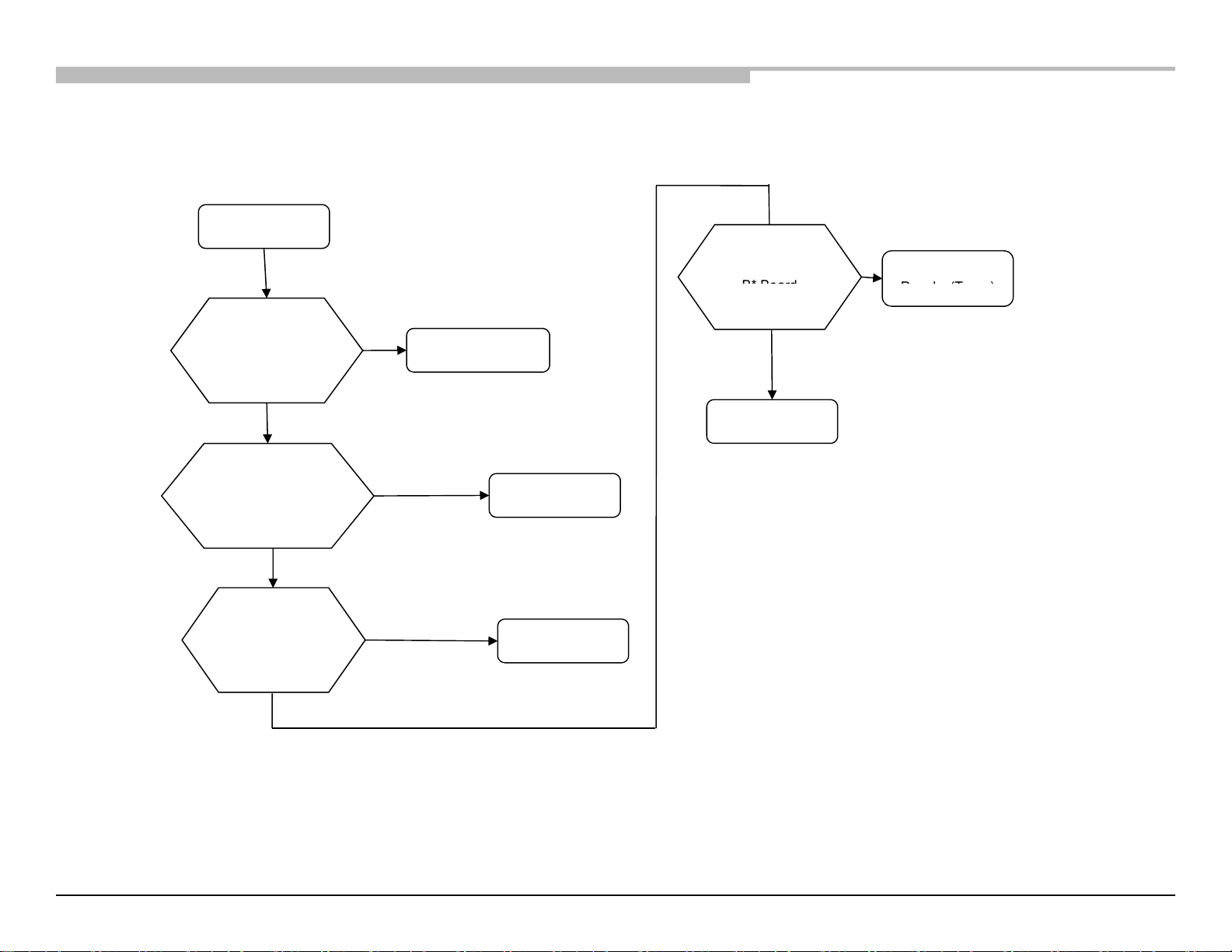
2.2-4 - LED BLINKING: 5X T-CON ERROR
Led Blinking
B* Board
P
l
(T
)
5-times blinking
Chassis: RB2G, HE-L
PANEL_VCC 12.5V at
About 12.5V
Replace the Harness
Between G* /LD board
Check
CN8001 on
on the B* Board
OK
and B board
NG
Replace
the LVDS Harness
NG
G* Board/Adaptor
Symptom
improvement
Symptom
improvement
Harness
LVDS Harness
Change
Symptom
improvement
B*Board
NG
Change
ane
Confirm Tcon12V.
-con
Chassis: RB2G, HE-L 43
NG
Page 44
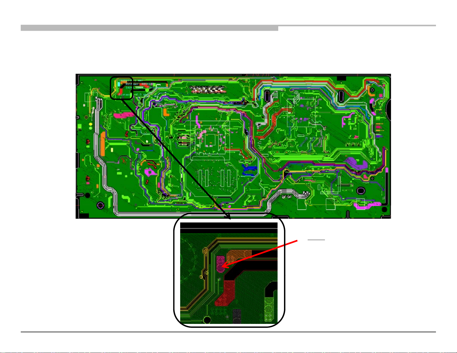
BAX-L BOARD (Side-B)
RB2G CHASSIS
W700B/ W800B
Troubleshooting
BAXL Probi
ng Points
BAXL (B
-
Side)
BAX-L PROBING POINTS
Chassis: RB2G, HE-L
JL9132
(PANEL_VCC)
Chassis: RB2G, HE-L 44
Page 45
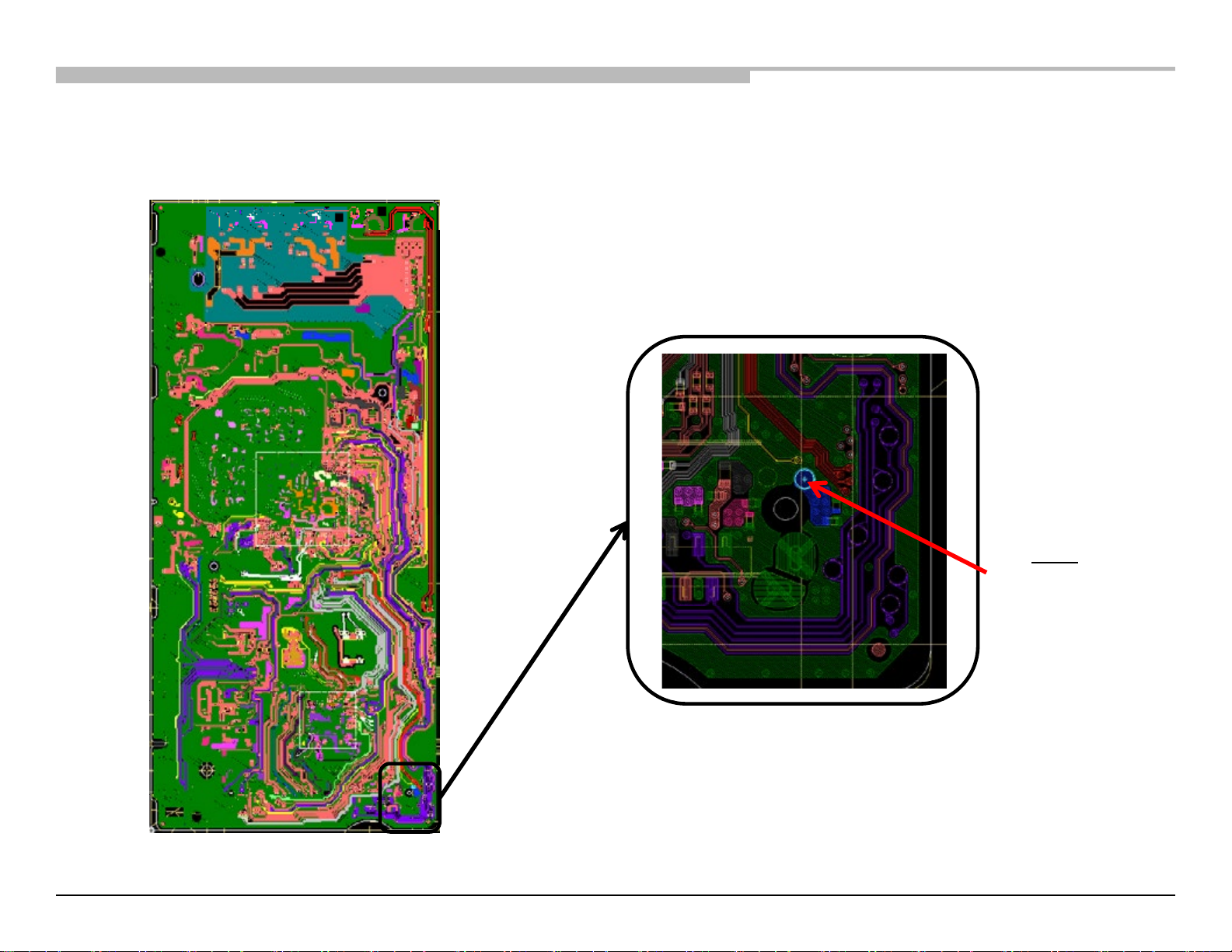
RB2G CHASSIS
W700B/ W800B
Troubleshooting
BAX Probing Points
BAX (B-Side)
BAX BOARD (Side-B)
BAX PROBING POINTS
Chassis: RB2G, HE-L
JL9137
(PANEL_VCC)
Chassis: RB2G, HE-L 45
Page 46
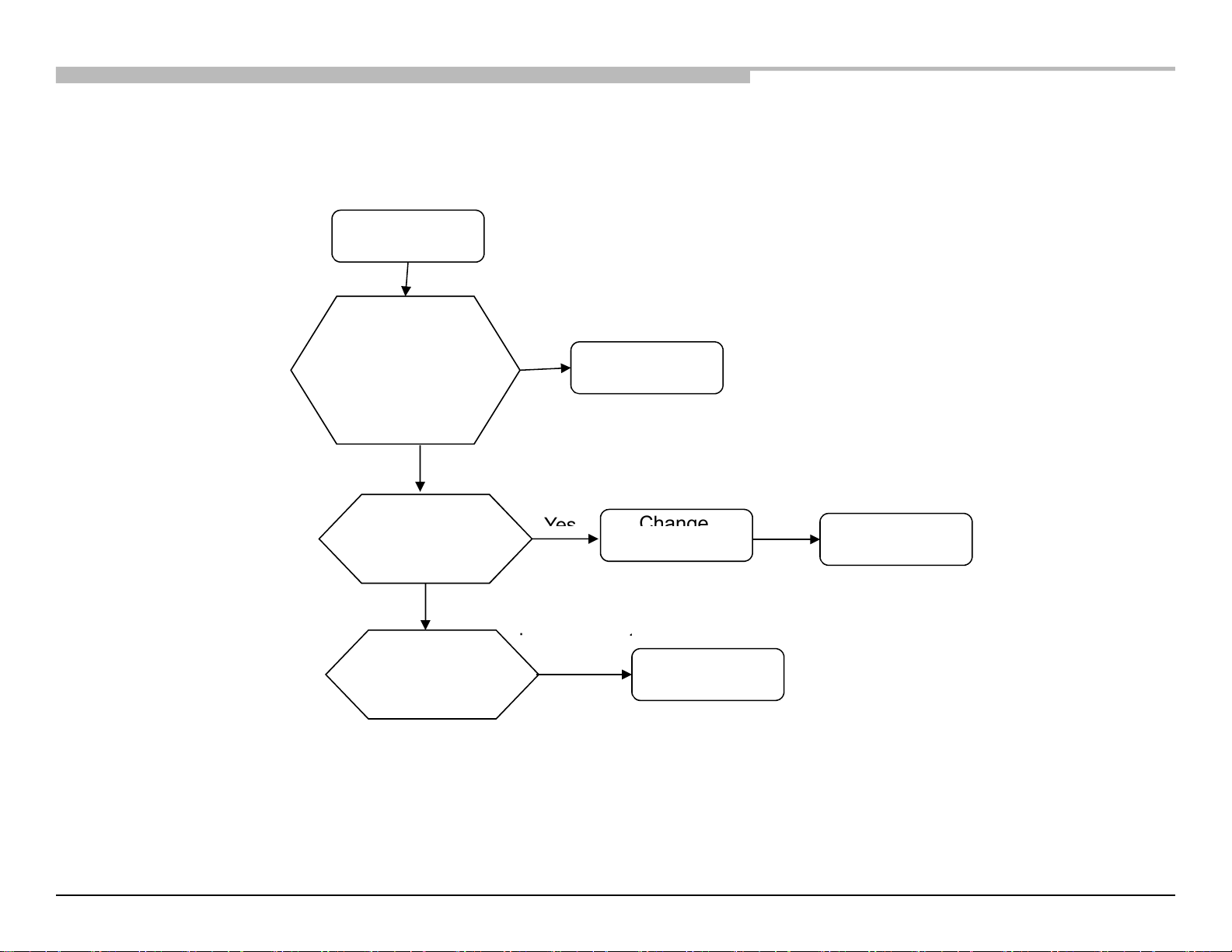
2.2-5 - LED BLINKING: 6X BACKLIGHT ERROR
Change
Yes
i
t
6-time blinking
Check JL9106* at
(BACKLIGHT_MON)
of CN9101
on the B* Board
Chassis: RB2G, HE-L
B* Board
1.3 -1.8 V
Symptom
improvement
Have G board?
No
G* board
Symptom
G Board
mprovemen
Change LD Board LD Board
Chassis: RB2G, HE-L 46
Page 47
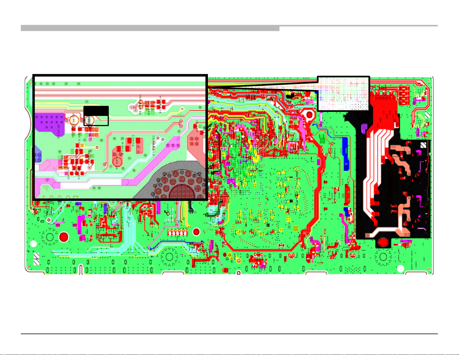
RB2G CHASSIS
W700B/ W800B
Troubleshooting
BAX: B Side
BAX BOARD (Side-B)
Chassis: RB2G, HE-L
JL9106
Chassis: RB2G, HE-L 47
Page 48
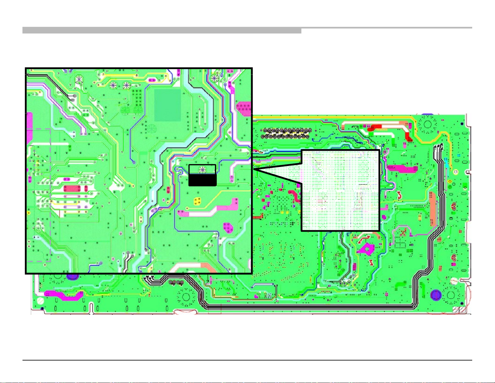
A
U
U
BAX-L BOARD (Side A)
Chassis: RB2G, HE-L
Y
2
JL9106
Chassis: RB2G, HE-L 48
Page 49
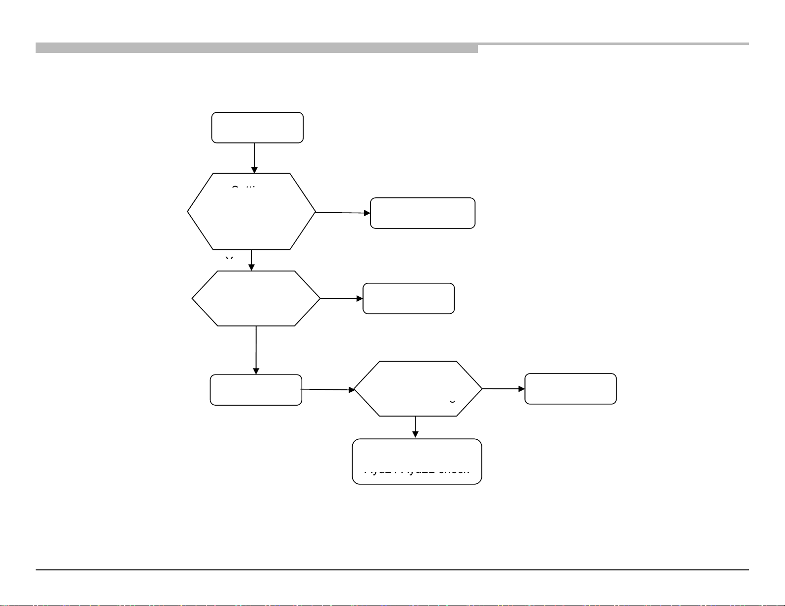
2.2-6 - LED BLINKING: 7X TEMPERATURE ERROR
RB2G CHASSIS
W700B/ W800B
Troubleshooting
2-2-6. 7x (Temperature Error)
2-2. Led Blinking
Setti
Y
g
g
Ayu2 / Ayu2L
check
7-time blinking
ng
circumstance is OK?
Temperature,
Ventilation, etc.
es
No
Chassis: RB2G, HE-L
Set to another
location, etc.
Change B* Board,
and Aging a few
hours
Symptom
improvement
B* Board
NG
Panel
I2CA bus check:
HDMI is workin
?
No
I2CA bus dumping or
Yes
Temp sensor
IC7001
Chassis: RB2G, HE-L 49
Page 50
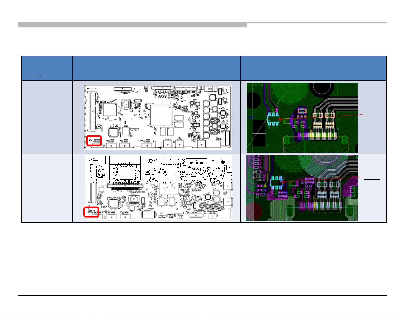
Chassis: RB2G, HE-L
RB2G CHASSIS
W700B/ W800B
Troubleshooting
Name
Board
BAX
(IC7001)
BAXL
(IC7001)
Board PWB (A side) Detail
IC7001
IC7001
Chassis: RB2G, HE-L 50
Page 51
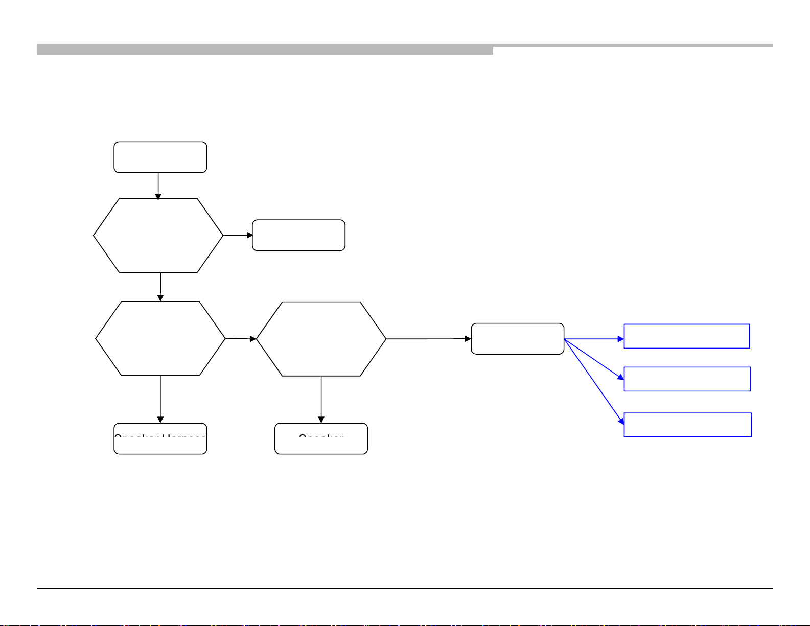
2.3-1 - NO SOUND:GENERAL
RB2G CHASSIS
W700B/ W800B
Troubleshooting
2-3-1. General
2-3. No Sound
Speaker Harness
Speaker
Chassis: RB2G, HE-L
“TV Speakers”
No Sound
Check the
“Speakers setting”
Change the Speaker
Harness
improvement
“Audio System”
Change to
“TV Speaker”
NG
the B* Board
Replace
NGSymptom
Symptom
improvement
B* Board
No Sound: Audio
No Sound: Tuner
No Sound: HDMI
Chassis: RB2G, HE-L 51
Page 52
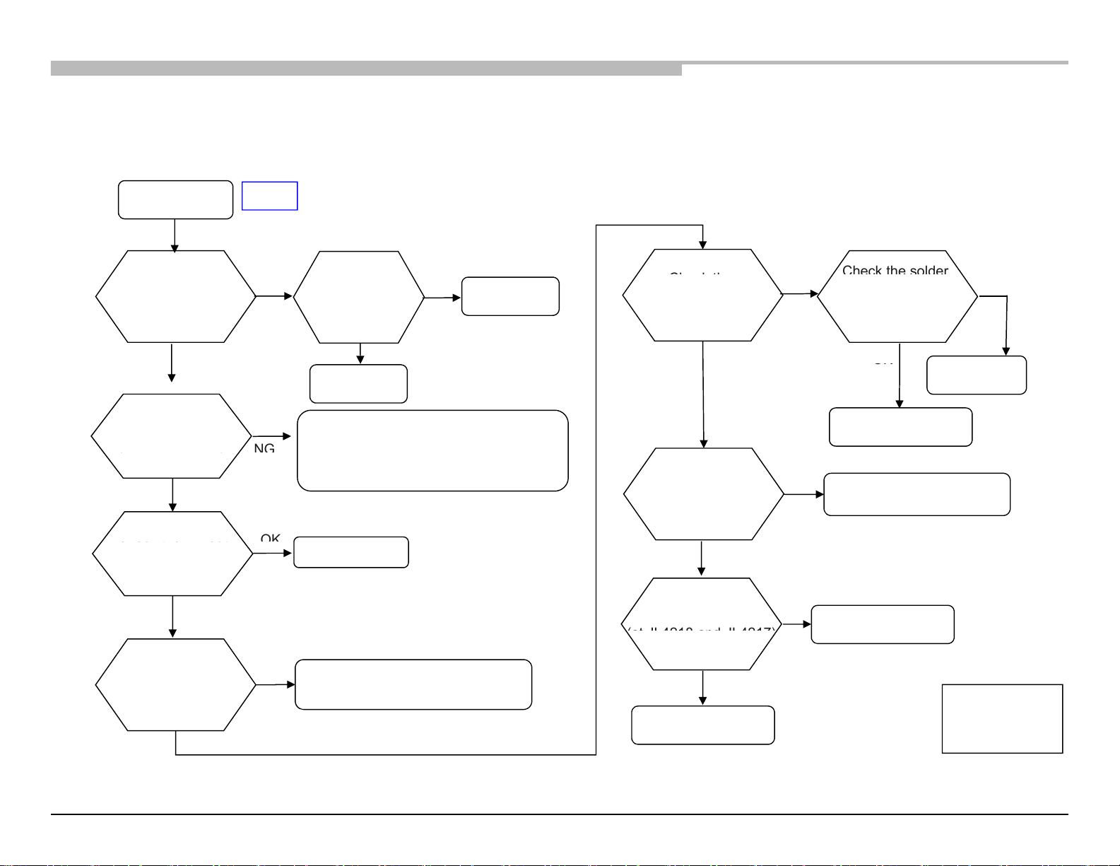
2.3-2 - NO SOUND: AUDIO (FOR ALL MODELS) TUS AND BAX (HT-L, HT-H, HT-H65, HS)
RB2G CHASSIS
W700B/ W800B
2-3-2. Audio (For all models) TUS, TUW and BAX (HT-L, HT-H, HT-H65, HS)
2-3. No Sound
Check th
Check the solder
(
)
OK
NG
( p)
Check the HP out
OK
(at JL4218
and J
L4217)
Chassis: RB2G, HE-L
#1
#1
Check the
Digital out
(use Video input)
OK
Check the
Speaker Sound
use Video input
OK
(use Video input)
NG
No signal
Check the
CN3103 pin1
(SPDIF input)
OK
CN3103 is NG
Power Amp Block
(F4401,IC4901,F4402,IC4902 etc)
is NG. See item: LED blinking 3x
No Problem
No signal
IC9000 is NG
(Audio error)
e
IC4204 VSS -3.3V
(IC4204 pin6)
OK
Check the
X_AUDIO_MUTE_
SPHPLO
pin5 is HIGH?
OK
Check the
INR+ & INL+ pin1 &14.
NG
NO
No signal
of IC4204 CP & CN
(7&8pin) & C4244
Solder NG
IC4204 NG
This is MUTE situation.
Check IC9000
IC9001 is NG
NG
Chassis: RB2G, HE-L 52
Check the IC4204
VDD 3.3V
(IC4204 pin9)
OK
NG
DC/DC converter is NG
See No POWER DC / DC
Converter Check
Signal is coming?
OK
IC4204 NG
Note:
(AYU2/Ayu2L) –
IC9000
(Brownie)- IC9001
Page 53
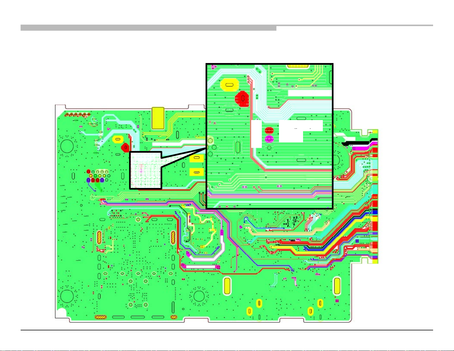
RB2G CHASSIS
W700B/ W800B
TUS board Side B
V
in (pin 1
)
3
(p )
Vcc
CN31
0
TUS BOARD (Side B)
Chassis: RB2G, HE-L
Chassis: RB2G, HE-L 53
Page 54
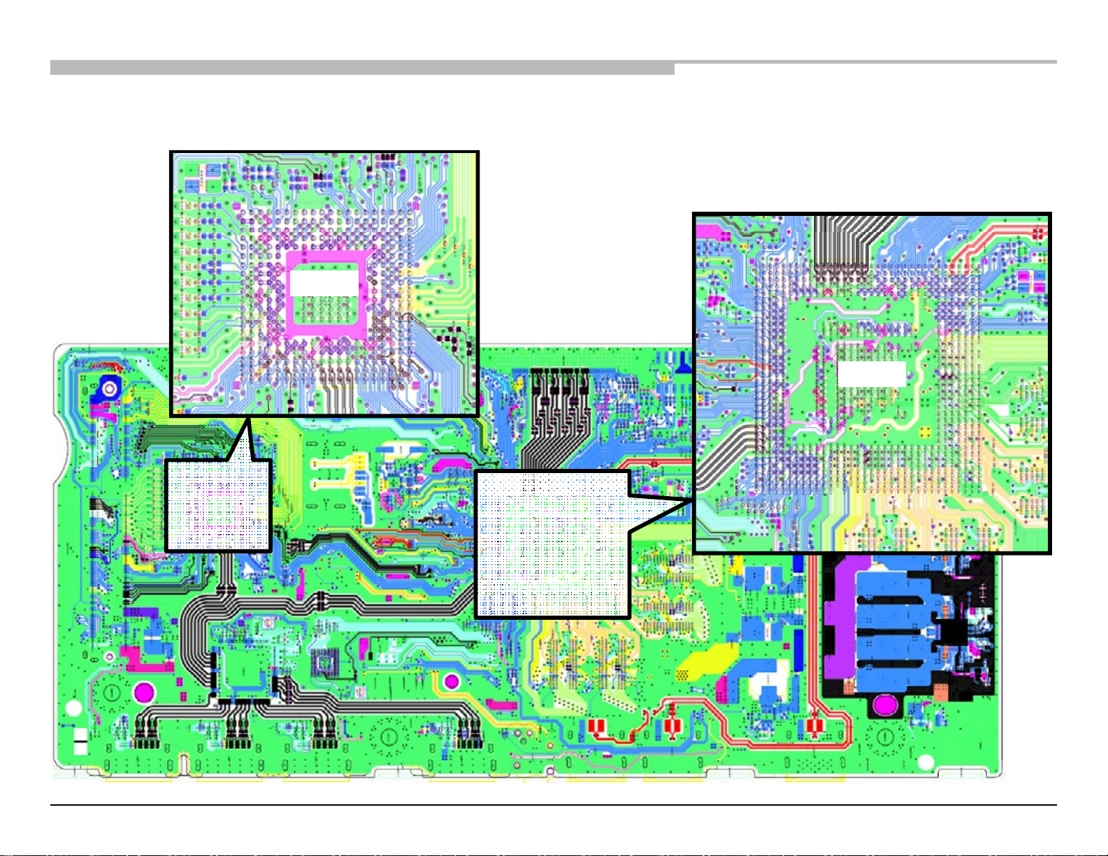
IC9001
1
IC9000
1
BAX BOARD (Side A)
Chassis: RB2G, HE-L
Chassis: RB2G, HE-L 54
Page 55
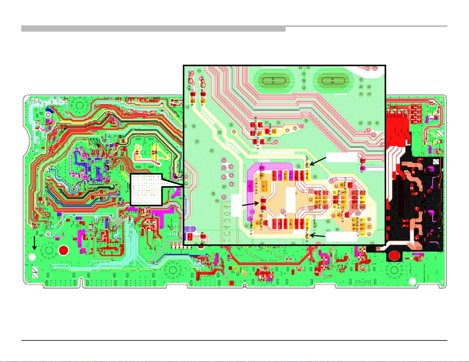
RB2G CHASSIS
W700B/ W800B
Troubleshooting
BAX board Side B
L4402
1
36
39
JL4217
46
IC
4
9
8
F440
1
L4401
4
204
6
7
C4244
5
1
JL4218
BAX BOARD (Side B)
Chassis: RB2G, HE-L
Chassis: RB2G, HE-L 55
Page 56
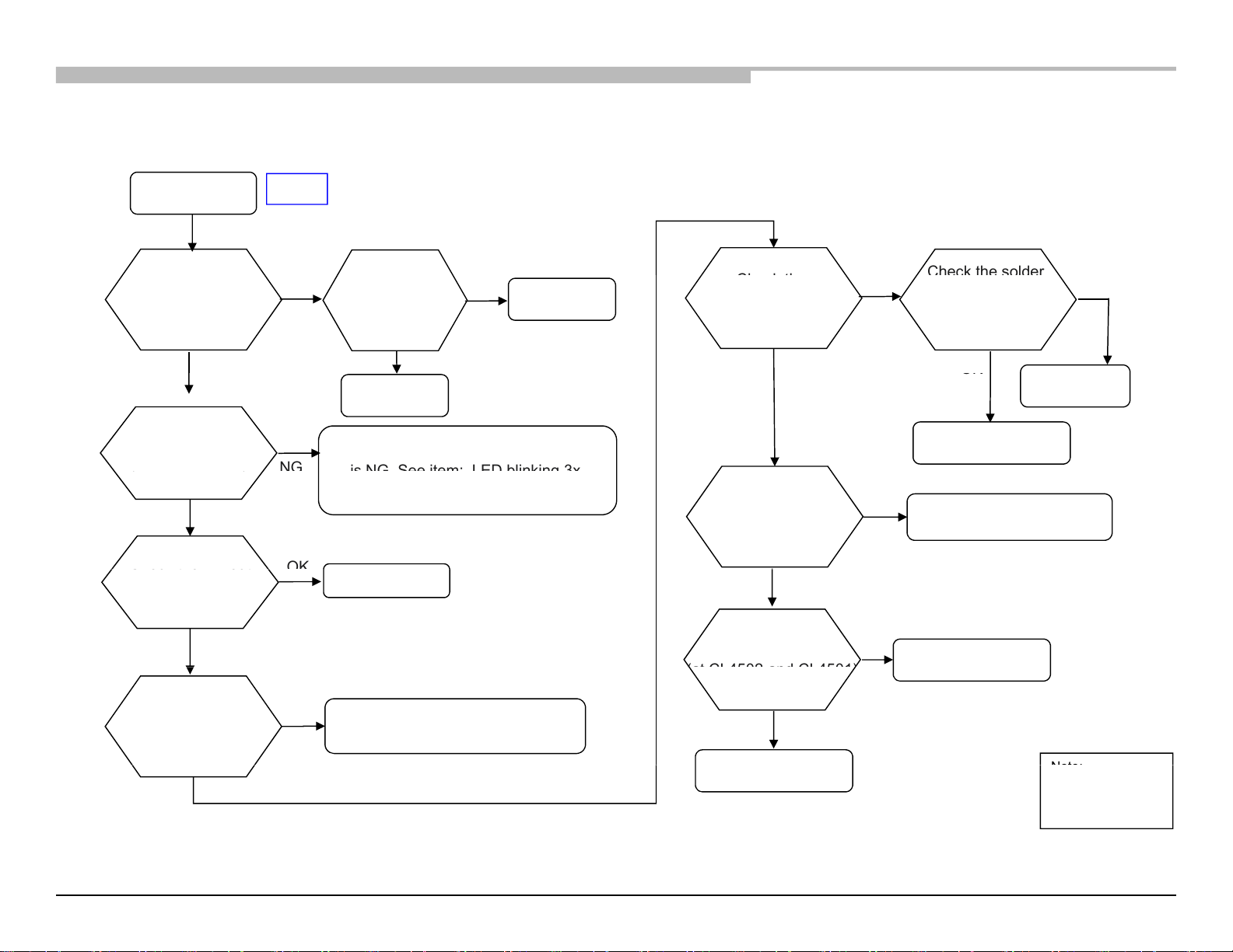
2.3-3 - NO SOUND: AUDIO (FOR ALL MODELS) BAX-L (HE-L, HM, HE-H) BOARD ONLY
RB2G CHASSIS
W700B/ W800B
2-3-3. Audio (for all model) TUS,TU W & BAX-L(HE-L,HM,HE-H) board only
2
-
3
. No
Sound
Check
Check the solder
(
put)
OK
NG
( p )
is
See item
: LED
blinking
3x
Check
the
out
OK
(at CL4502 and CL4501)
Note:
Chassis: RB2G, HE-L
#1
#1
Check the
Digital out
(use Video input)
OK
Check the
Speaker Sound
use Video in
OK
HP
(use Video input)
NG
No signal
Check the
CN3103 pin1
(SPDIF input)
OK
CN3103 is NG
Power Amp Block (F4601,IC4601,etc)
NG.
No Problem
No signal
IC9000 is NG
(Audio error)
the
IC4501 VSS -3.3V
(IC4501 pin6)
OK
Check the
X_AUDIO_MUTE_
SPHPLO
pin5 is HIGH?
OK
Check the
INR+ & INL+ pin1 &14.
NG
NO
No signal
of IC4501 CP & CN
(7&8pin) & C4501
IC4501 NG
This is MUTE situation.
Check IC9000
IC9001 is NG
Solder NG
NG
Check the IC4501
VDD 3.3V
(IC4501 pin9)
OK
Chassis: RB2G, HE-L 56
NG
DC/DC converter is NG
See No POWER DC / DC
Converter Check
Signal is coming?
OK
IC4501 NG
(AYU2/Ayu2L) –
IC9000
(Brownie)- IC9001
Page 57
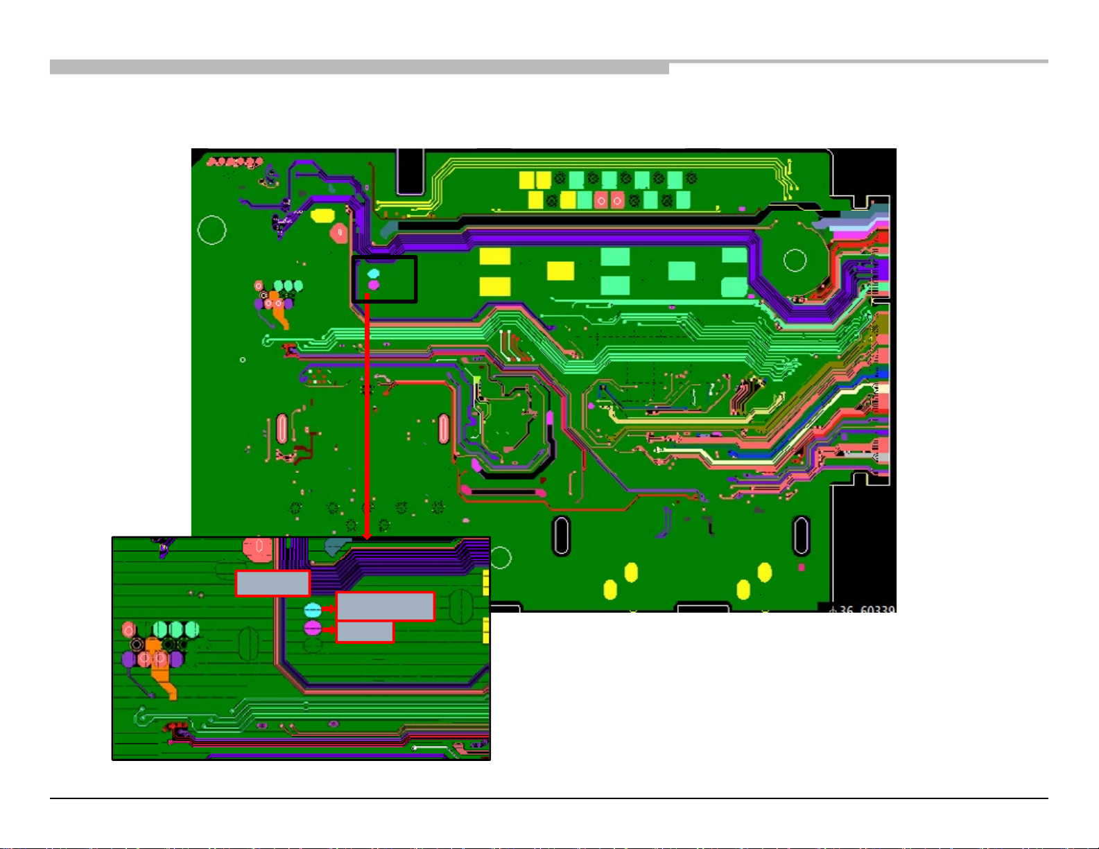
RB2G CHASSIS
W700B/ W800B
Troubleshooting
TUS board Side B
TUS BOARD (Side B)
Chassis: RB2G, HE-L
CN3103
Vin (pin 1)
Vcc
Chassis: RB2G, HE-L 57
Page 58
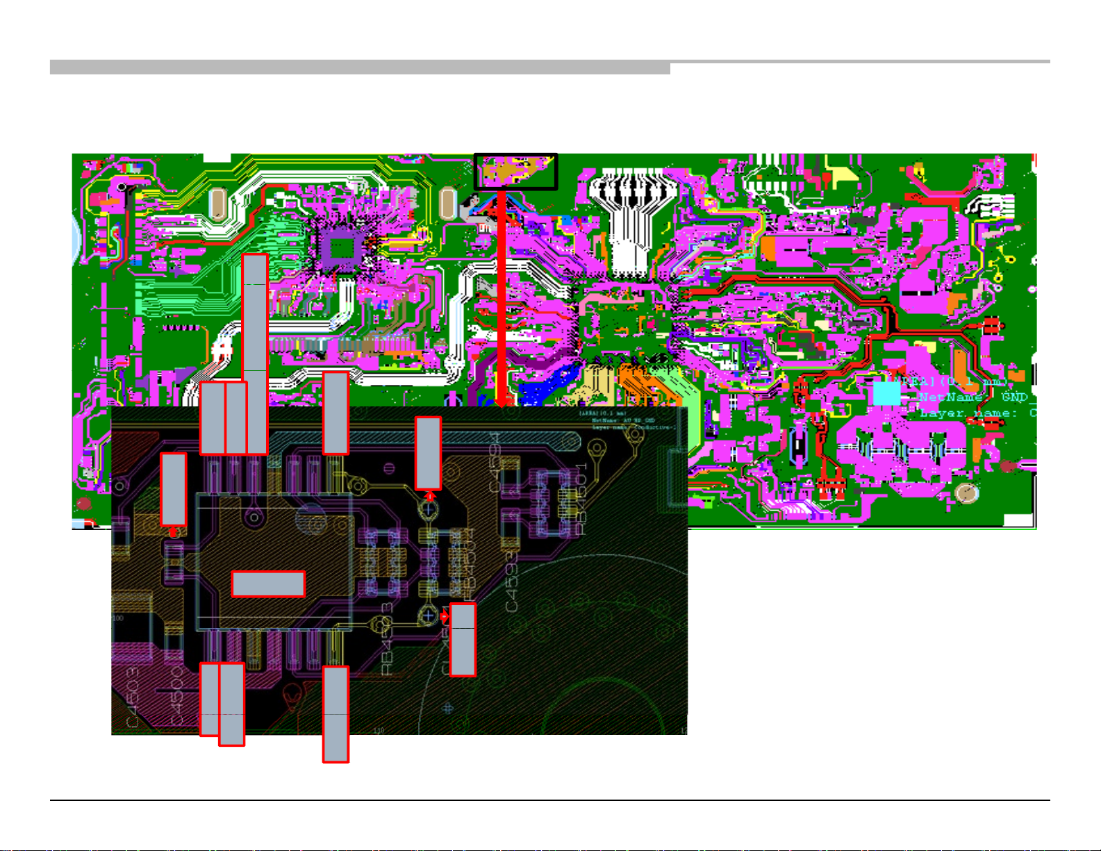
RB2G CHASSIS
W700B/ W800B
Troubleshooting
BAX-L board Side A
in 5)
_MUTE_SPHLO (
P
INR+ (Pin1)
X_AUDIO_MUT
E
Vss (Pin 6)
CN (Pin 7)
502
C4501
CL
4
IC4501
01
(Pin 8)
(Pin 9)
Pin14)
CL45
C
P
VD
D
INL+
(
BAX-L BOARD (Side A)
Chassis: RB2G, HE-L
Chassis: RB2G, HE-L 58
Page 59
Chassis: RB2G, HE-L
RB2G CHASSIS
W700B/ W800B
Troubleshooting
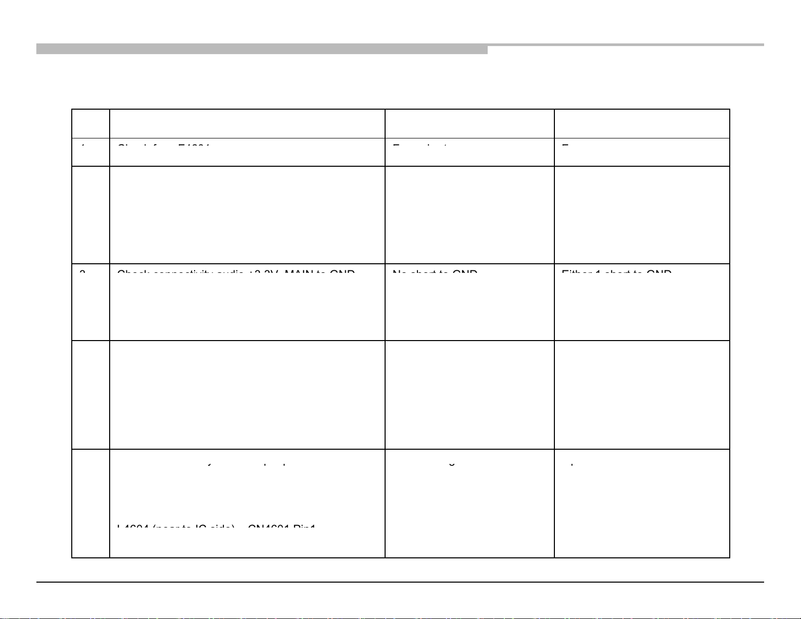
2-3-5. Main Board Power Off Checking (for Main SP Lch & Rch) for BAX-L (HEL,HEH,HM) board only
2-3. No Sound
1
Check
f
F4601
F
t
F
–
3
Check connectivity
audio
+3.3V_MAIN to GND
No short to GND
Either 1 short to GND
y
y
pp
g
p
L4604 (near to IC side)
–
CN4601 Pin1
2.3-4 - NO SOUND: MAIN BOARD POWER OFF CHECKING (MAIN SPEAKER L & R) FOR BAX-L (HEL, HEH, HM) BOARD ONLY
No Checking Item OK NG
use
2 Check connectivity audio Vcc to GND
use shor
use open
No short to GND Either 1 short to GND
C4606 – GND
C4607
GND
C4608 – GND
C4609 – GND
(only for BAX-L board)
IC4601 (Pin8) – GND
IC4601 (Pin27) – GND
4 Check connectivity audio output to GND.
No short to GND Either 1 of pin short to GND
CN4601
Pin 1 – GND
Pin 2 – GND
Pin 3 –GND
Pin 4 – GND
5 Check connectivit
Chassis: RB2G, HE-L 59
audio output path Must havegood connection Open circuit.
(only for BAX-L board):
L4601 (near to IC side) – CN4601 Pin4
L4602 (near to IC side) – CN4601 Pin3
L4603 (near to IC side) – CN4601 Pin2
(~0 Ω)
Page 60
RB2G CHASSIS
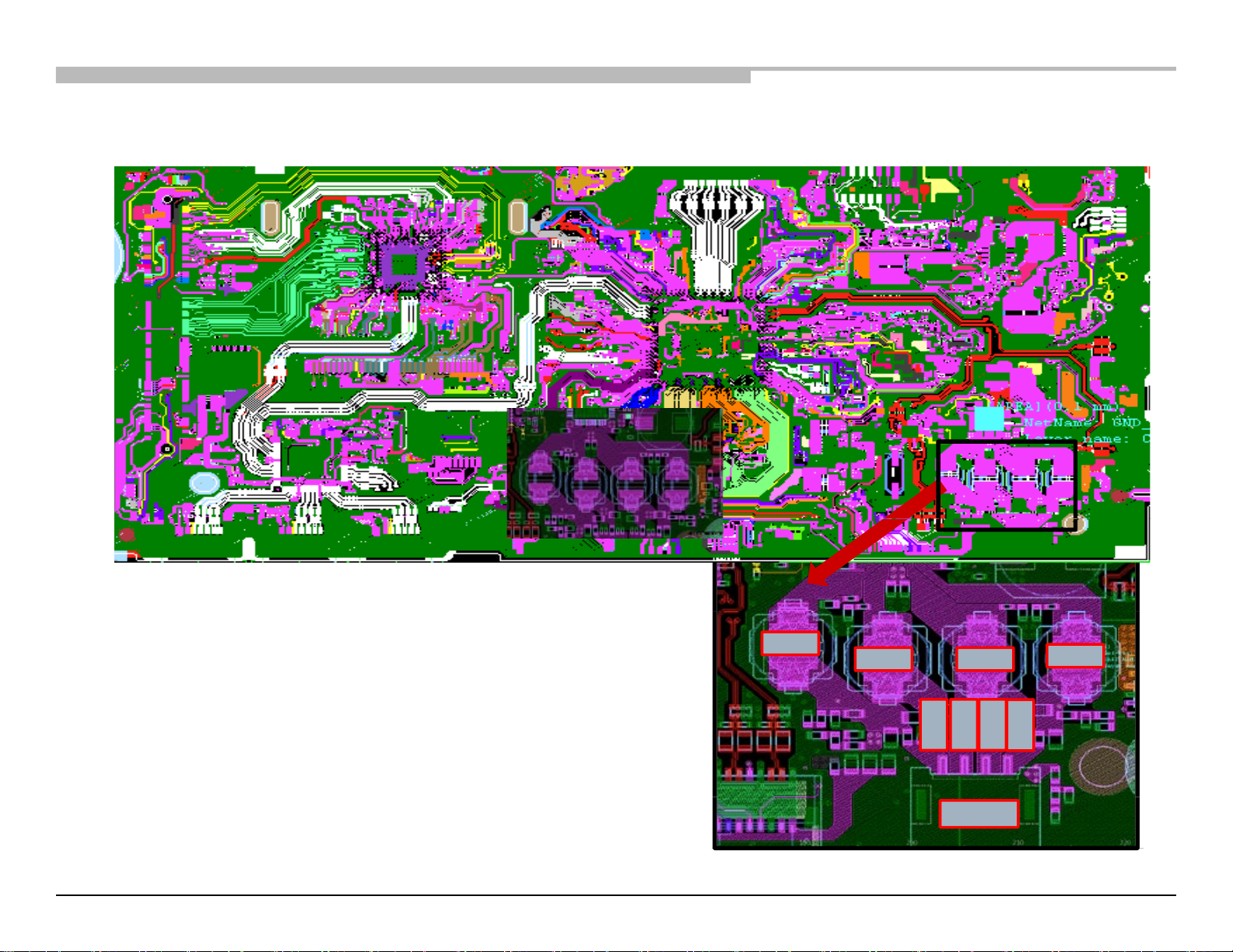
W700B/ W800B
Troubleshooting
BAX-L board Side A
L4604
L4603 L4602
L4601
Pin 1
Pin 2
Pin 3
Pin 4
CN4601
BAX-L BOARD (Side A)
Chassis: RB2G, HE-L
Chassis: RB2G, HE-L 60
Page 61
Chassis: RB2G, HE-L
RB2G CHASSIS
W700B/ W800B
Troubleshooting
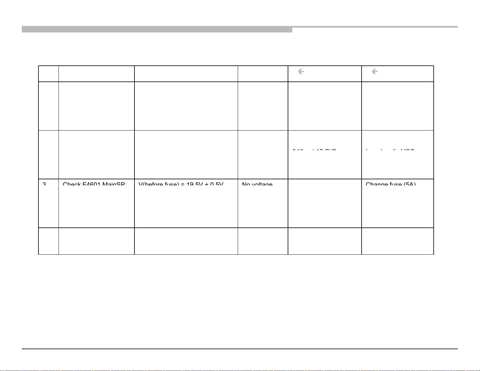
2-3-6. Main Board Power Off Checking (for Main SP Lch & Rch) for BAX-L (HEL,HEH,HM) board only
2-3. No Sound
&10
5V?
b
VCC
3
Check F4601
MainSP
V(before fuse) = 19.5V
±
0.5V
No
voltage
Change
fuse (5A)
2.3-5 - NO SOUND: MAIN BOARD POWER OFF CHECKING (MAIN SPEAKER L & R) FOR BAX-L (HEL, HEH, HM) BOARD ONLY
No Checking Item OK NG If NG If NG
1 Check
2 Check F4601 MainSP
IC4601 side-terminal of
L4601,L4602,
L4603,L4604
(for BAX-L only)
Switching Freq = 384kHz or
768KHz ±20KHz
Vrms = don’t care
V(before fuse) = 12.5V ± 0.5V
V(after fuse) = 12.5V ± 0.5 V
No switching
Go to next checking.
frequency at
either one of
the CL
No voltage. Check fuse broken?
Check CN9101 Pin 8
got 12.
(BAX-L board only)
4 Check IC4601 (Pin
8) and C4601 (Pin 27)
V(after fuse) = 19.5V ± 0.5V
V(before fuse) = 3.3V ± 0.5V
V(after fuse) = 3.3V ± 0.5V
.
No voltage. Check +3.3V_MAIN
(for BAX-L board only)
Change fuse (5A).
Check power supply
oard audio
.
.
Check power supply
board audio VCC.
supply.
Chassis: RB2G, HE-L 61
Page 62
Chassis: RB2G, HE-L
RB2G CHASSIS
W700B/ W800B
Troubleshooting
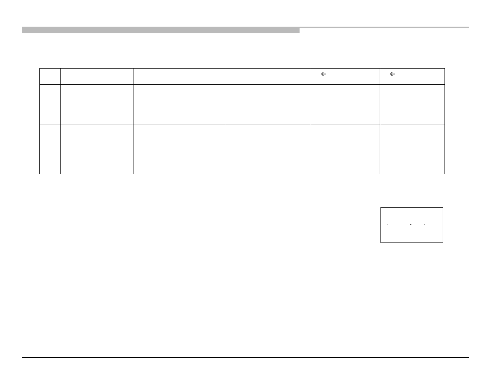
2-3-6. Main Board Power On Checking (for Main SP Lch & Rch) for BAX-L (HEL,HEH,HM) board only
2-3. No Sound
A
(
–
( y)
2.3-5 - NO SOUND: MAIN BOARD POWER OFF CHECKING (MAIN SPEAKER L & R) FOR BAX-L (HEL, HEH, HM) BOARD ONLY
No Checking Item OK NG If NG If NG
5 Check CL4605,
CL4606, CL4607
6 Check CL4601,
CL4602, CL4603,
CL4604
Vdc = 3.3V ± 0.3V Vdc < 0.8V CL4606 NG,
Check IC4601
CL4601 = 12.288MHz
CL4603 = 3.072MHz
CL4604 = 48KHz
CL4602 = moving CLK
ll Vp-p ≈ 3.3V make sure sound source
If no frequency at CL4601,
CL4603, CL4604, Ayu2 IC
(IC9000) NG.
If no frequency at CL4602,
OK.
If sound source OK,
but CL4602 = NG,
Ayu2 IC (IC9000) NG.
CL4605,4607 NG,
Check IC9000
Note:
AYU2/Ayu2L)
IC9000
(Brownie)- IC9001
Chassis: RB2G, HE-L 62
Page 63
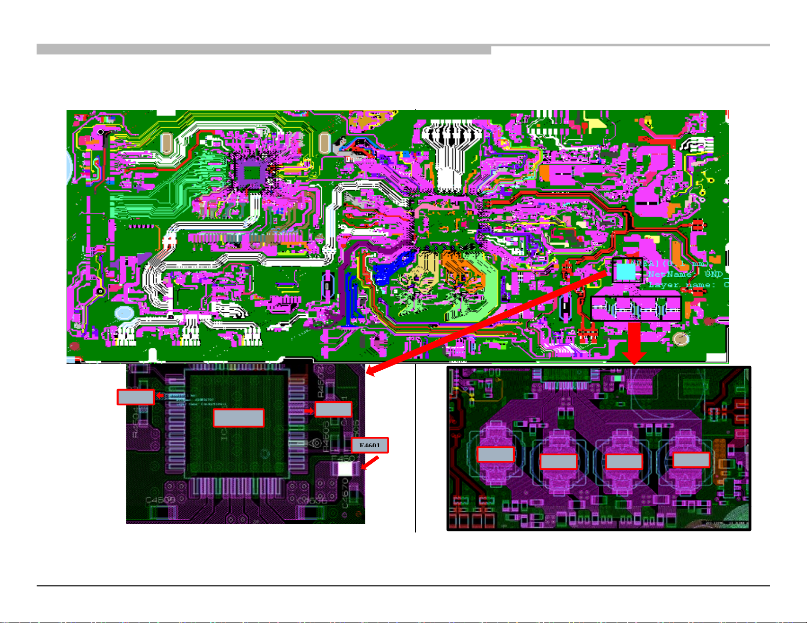
RB2G CHASSIS
W700B/ W800B
Troubleshooting
BAX
-
L board Side A
F4601
BAX-L BOARD (Side A)
Chassis: RB2G, HE-L
Pin 27
Chassis: RB2G, HE-L 63
25
36
37
24
IC4601
48
13
12
Pin 8
L4604
1
L4603 L4602
L4601
Page 64
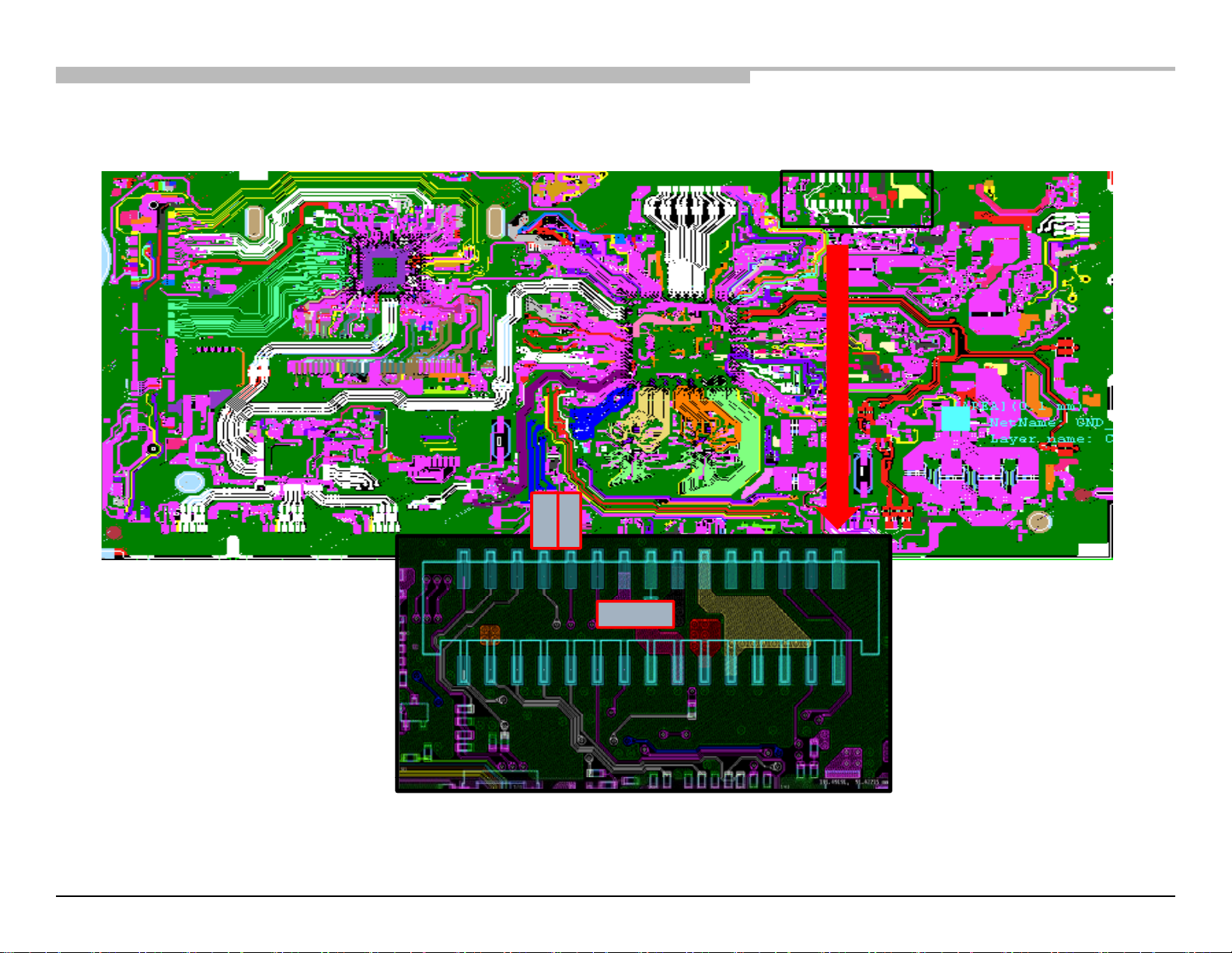
RB2G CHASSIS
W700B/ W800B
Troubleshooting
BAX
-
L board Side A
0
BAX-L BOARD (Side A)
Chassis: RB2G, HE-L
Chassis: RB2G, HE-L 64
Pin 8
Pin 1
CN9101
Page 65
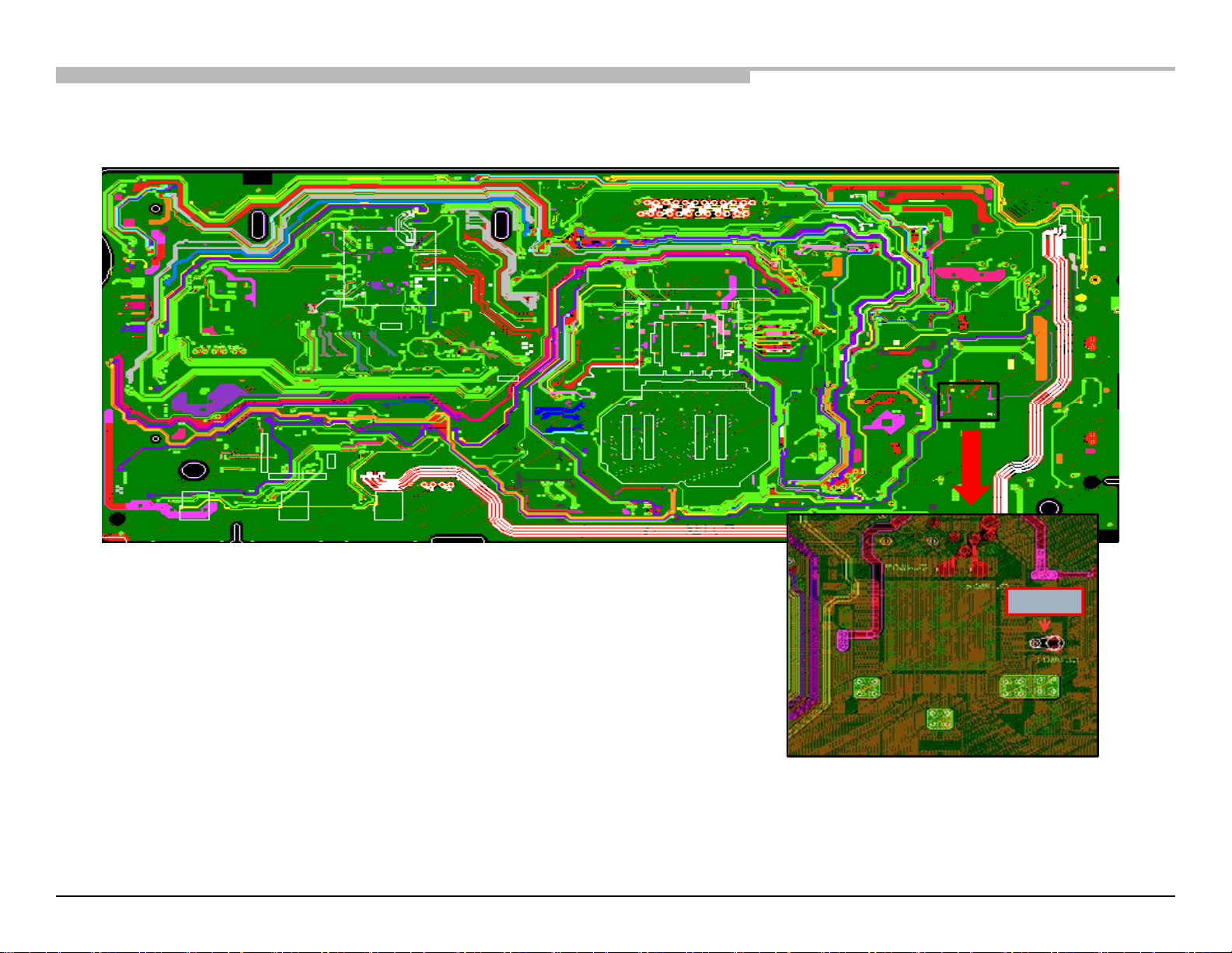
RB2G CHASSIS
W700B/ W800B
Troubleshooting
BAX-L board Side B
BAX-L BOARD (Side B)
Chassis: RB2G, HE-L
CL4601
Chassis: RB2G, HE-L 65
Page 66
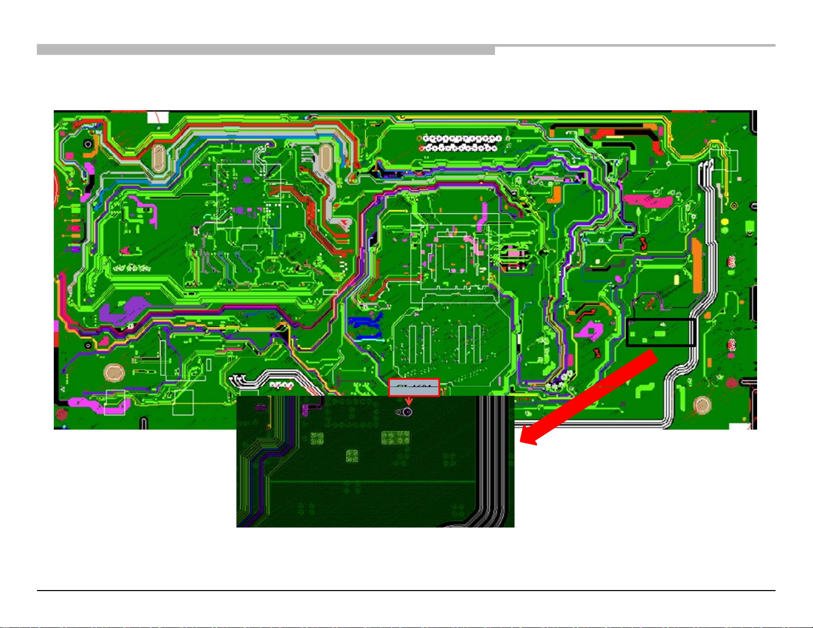
RB2G CHASSIS
W700B/ W800B
Troubleshooting
BAX-L board Side B
CL4601
BAX-L BOARD (Side B)
Chassis: RB2G, HE-L
Chassis: RB2G, HE-L 66
Page 67
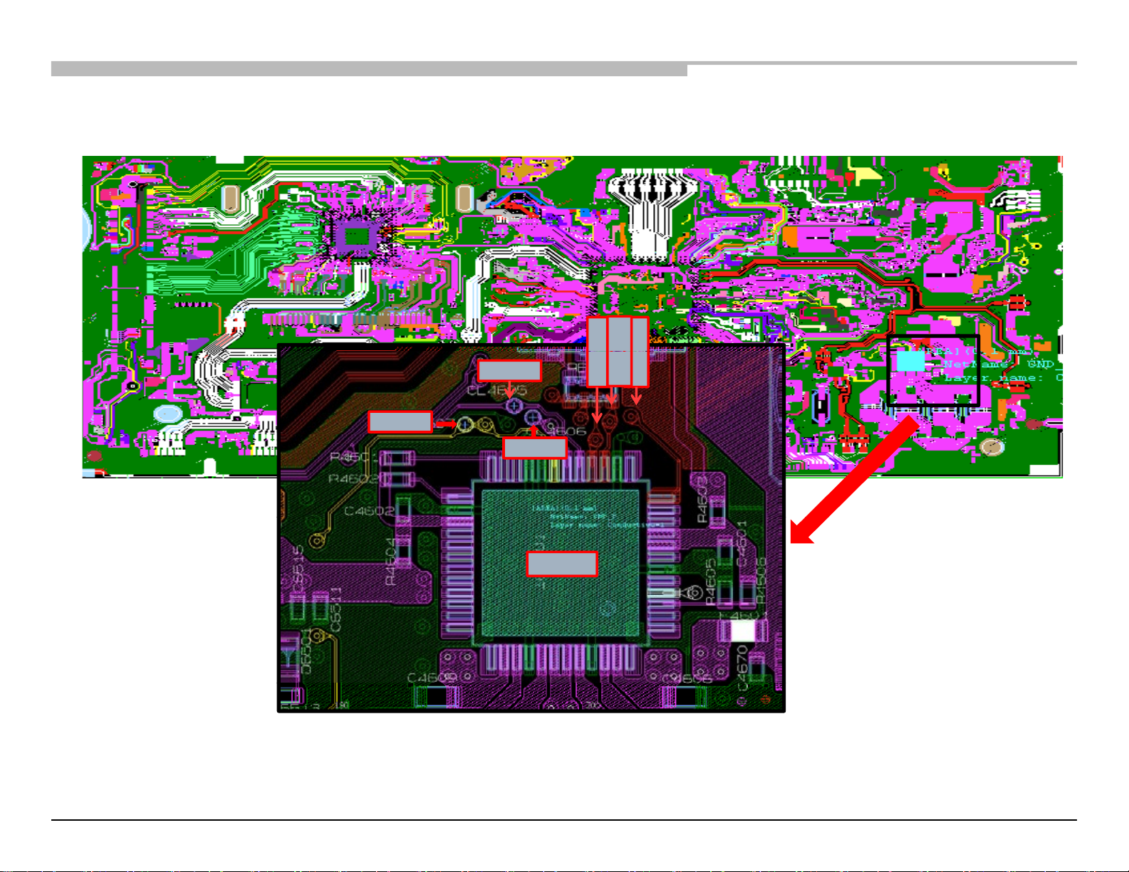
RB2G CHASSIS
W700B/ W800B
Troubleshooting
BAX-L board Side A
4CL4
4
BAX-L BOARD (Side A)
603
604
Chassis: RB2G, HE-L
602
CL4607
25
CL4605
CL4605
24
18
16
15
CL
CL
13
IC4601
36 1
48
37
39
41
44
46
12
4
Chassis: RB2G, HE-L 67
Page 68
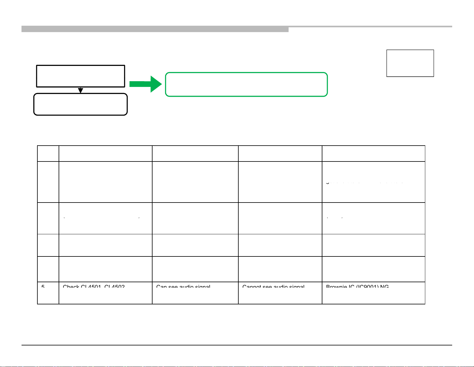
2.3-6 - NO SOUND: HP/LINEOUT ONLY FOR BAX-L (HEL, HEH, HM) BOARD ONLY
RB2G CHASSIS
W700B/ W800B
Troubleshooting
-
-
-
237
. No
Sound: HP / Lineout Only
for BAX
L (HEL,HEH,HM) board
only
got short to GND? If
short to GND
(
)
(
(
)
()
5
Check CL4501, CL4502
Can see audio signal
Cannot see audio signal
Brownie IC (IC9001)
NG
No Sound
RB1 Main Board Power On Checking
HP / Lineout only
BAX-LPower On checking
No Checking Item OK NG If NG
1 Insert HP Jack. Check R4508 Vdc = 3.3V ± 0.3V Vdc = 0V or < 1V Check HP_DET line
This is for Main SP got sound, but HP / Lineout no sound
Chassis: RB2G, HE-L
Note:
(AYU2/Ayu2L) –
IC9000
(Brownie)- IC9001
(R7020 – for BAX-L)
replace board.
2 Check IC4501 Pin 5
3 Check CL4505, CL4506.
(with audio signal input)
4 Check IC4501 pin 9 Vdc = 3.3V ± 0.3V No 3.3V supply. Please refer
(with audio signal input)
Chassis: RB2G, HE-L 68
X AUDIO MUTE SPHPLO
_ __
Vdc = 3.3V ± 0.3V Vdc = 0V or < 1V Check X_AUDIO_ MUTE_ SPHLO
Pin 5) short to GND. Ifshort to GND
replace board.
Can see audio signal
waveform
waveform
Cannot see audio signal
waveform
item 3-3-1. No POWER DC /
DC Converter Check
waveform
.
Go to below item No. 4 for checking
Page 69
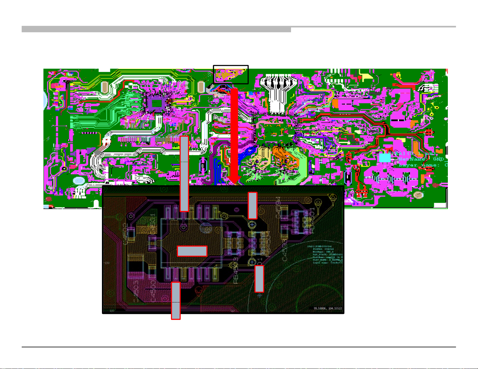
RB2G CHASSIS
W700B/ W800B
Troubleshooting
-
BAX
L board Side A
U
BAX-L BOARD (Side A)
Chassis: RB2G, HE-L
PLO (Pin 5)
Chassis: RB2G, HE-L 69
DIO_MUTE_ SPH
X_A
CL4502
IC4501
CL4501
(Pin 9)VDD
Page 70
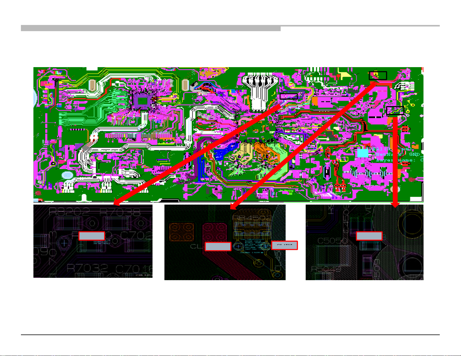
RB2G CHASSIS
W700B/ W800B
Troubleshooting
-
BAX
L board Side A
CL4505
BAX-L BOARD (Side A)
Chassis: RB2G, HE-L
Chassis: RB2G, HE-L 70
R4508R7020
CL4506
Page 71
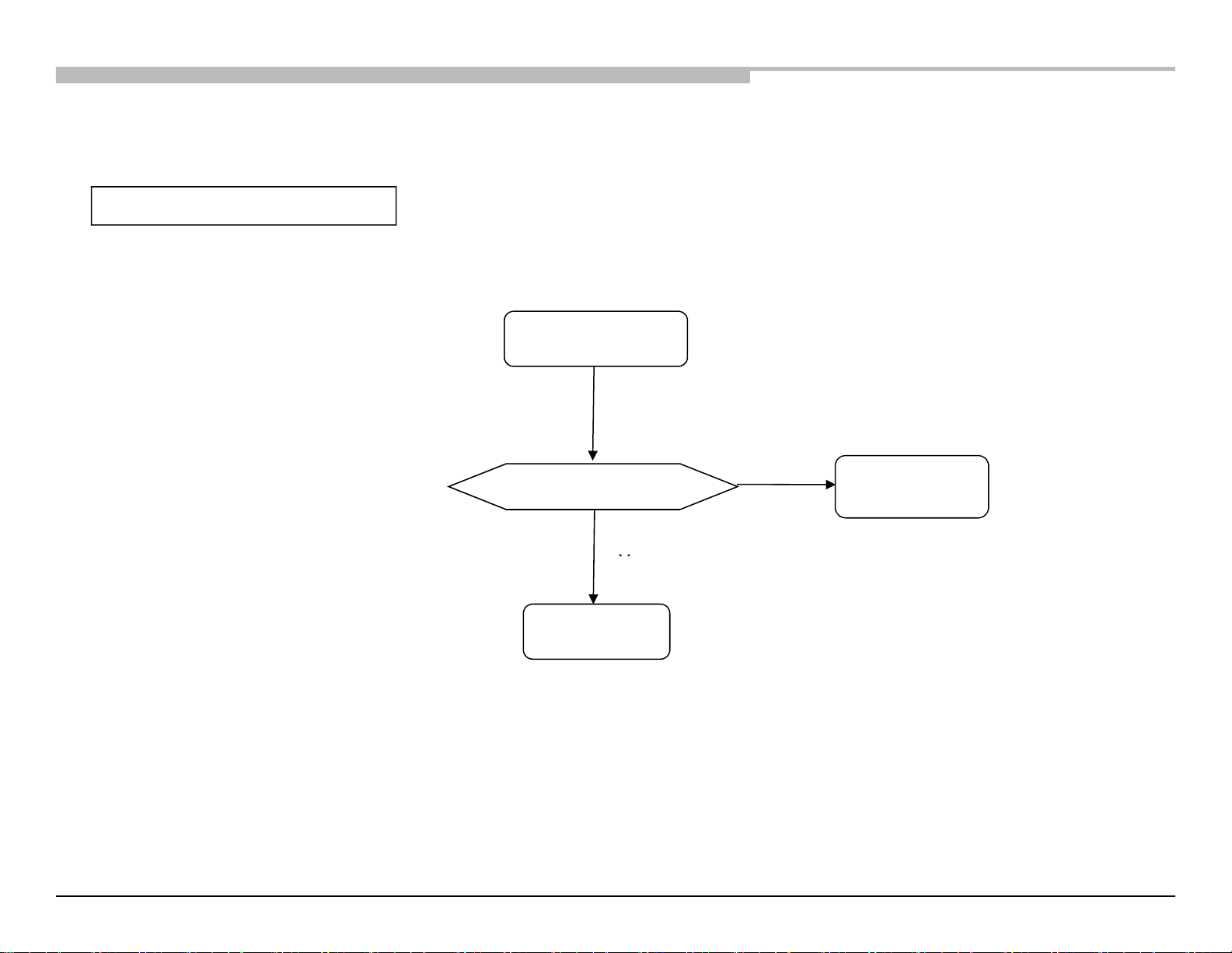
2.3-7 - NO SOUND: TUNER
-
7. No Sound: Tuner
Y
This troubleshooting is only for Analog
Chassis: RB2G, HE-L
No Sound
with normal picture
NO
Please refer audio
Only RF tuner input??
troubleshooting
es
Check Brownie
Chassis: RB2G, HE-L 71
Page 72
RB2G CHASSIS
W700B/ W800B
Troubleshooting
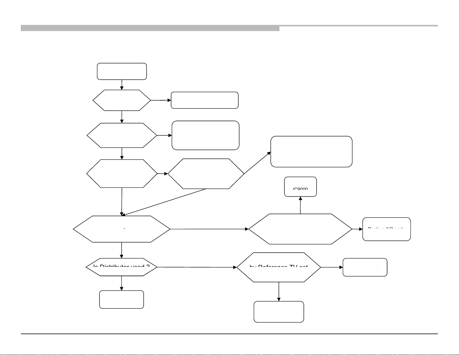
3-8. No Sound : HDMI
IC9000
Replace NG part
y
r
by Reference TV set
Is Distributor used ?
g
2.3-8 - NO SOUND: HDMI
No Sound
Check the picture
OK
Chassis: RB2G, HE-L
NG
Refer to HDMI NO PICTURE
Check the mode
of Source equipment
HDMI
Does this model have
YES
D-sub input ?
NO
Check Sound by other TV set
which is same model
NG
YES
Connect Source
equipment directly
DVI
Change the mode of
Source equipment to HDMI
What is set in
“HDMI/DVI Audio Source”
of Sound MENU ?
Auto or HDMI Audio
OK
NO
Change “HDMI/DVI Audio Source”
PC
to Auto
Audio
Replace
OK
Check R5071, C5071, C5072,
C5059, C5073
Check Source equipment
(For example, RB1)
NG
Check the settings of
Source equipment
OK
NG
Inform the designe
of it
Chassis: RB2G, HE-L 72
Page 73
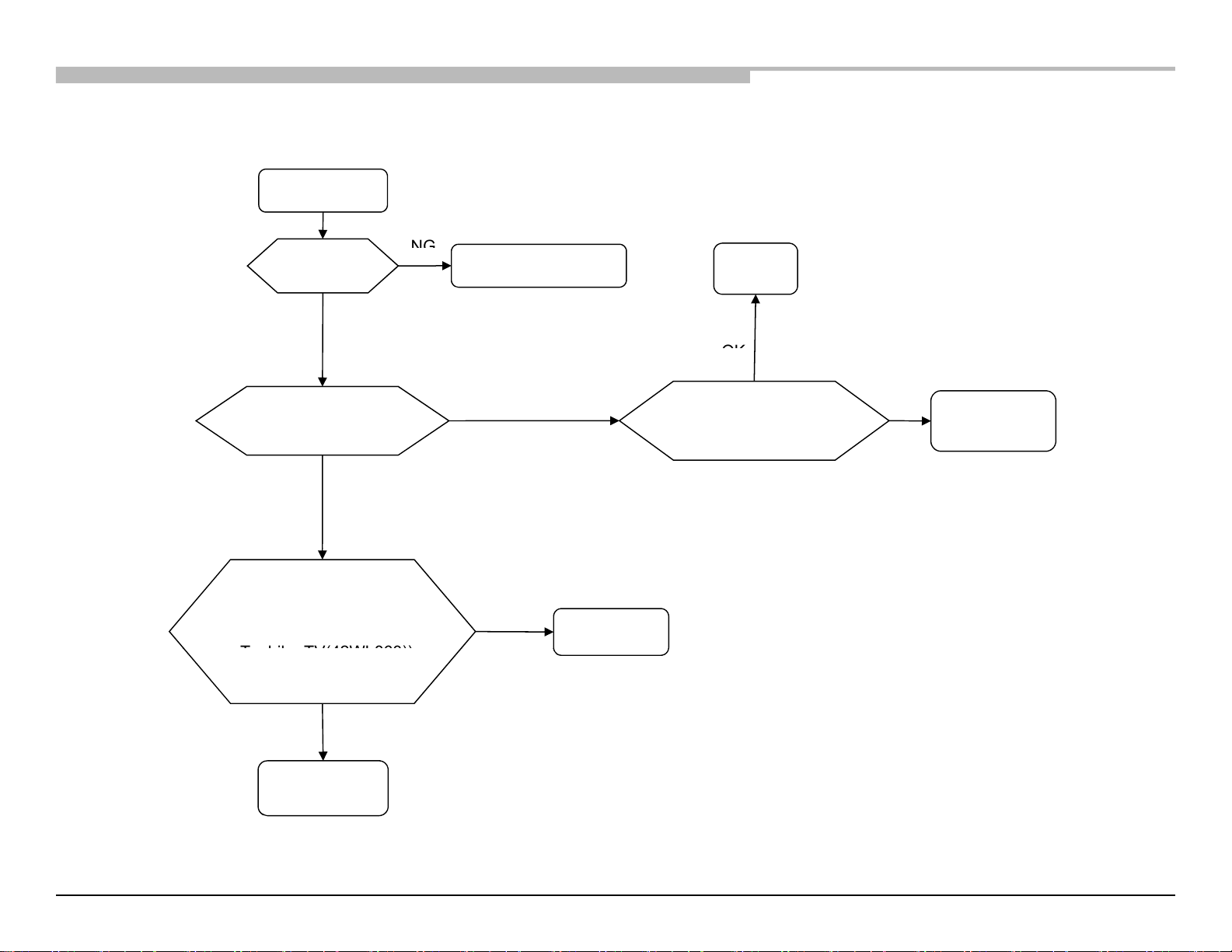
2.3-9 - NO SOUND: MHL
RB2G CHASSIS
W700B/ W800B
Troubleshooting
3-8. No Sound : MHL
NG
OK
hiba TV(42WL863))
Chassis: RB2G, HE-L
No Sound
Check the picture
OK
Check Sound by other TV set
which is same model
NG
Check Source equipment
by Reference TV set
(For example, Samsung TV(UN46ES7000)
, Tos
or VA-1836
Refer to MHL NO PICTURE
OK
OK
Check R5071, C5071, C5072,
Inform the designer
of it
Replace
IC9000
C5059, C5073
NG
Replace NG part
Chassis: RB2G, HE-L 73
NG
Check the settings of
Source equipment
Page 74
RB2G CHASSIS
W700B/ W800B
Troubleshooting
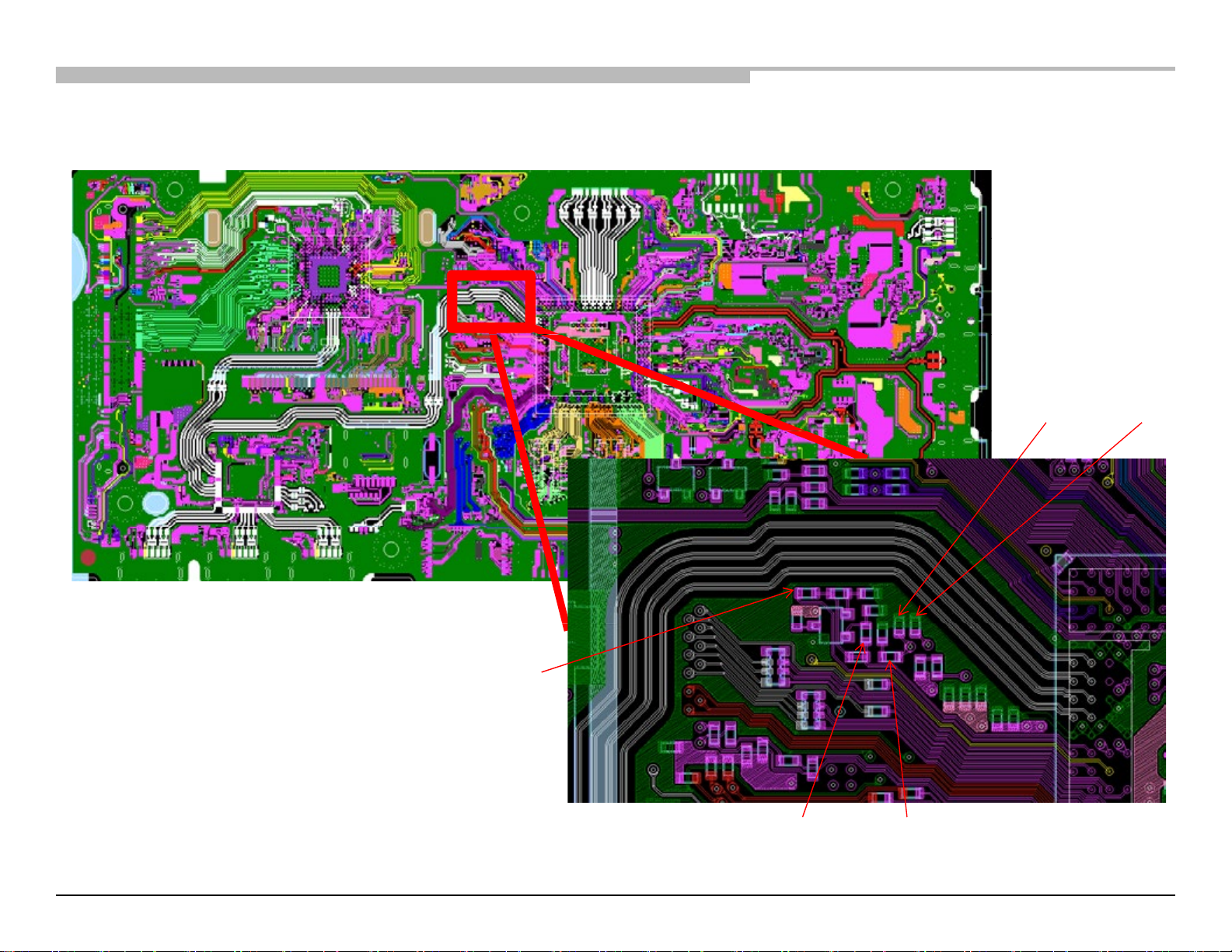
BAXLBAXL--A SideA Side
C5073C5072
C5059
BAX-L BOARD (Side A)
Chassis: RB2G, HE-L
C5059
C5071
R5071
C5072
C5073
Chassis: RB2G, HE-L 74
Page 75
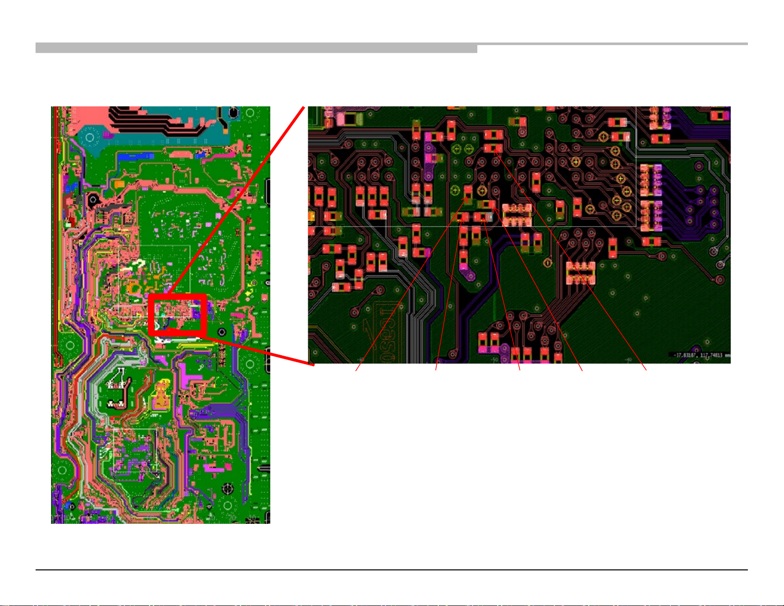
RB2G CHASSIS
W700B/ W800B
Troubleshooting
BAXBAX--B SideB Side
C5071
C5072
C5073
C5059
R5071
BAX BOARD (Side B)
Chassis: RB2G, HE-L
C5073 C5071 C5072 C5059R5071
Chassis: RB2G, HE-L 75
Page 76
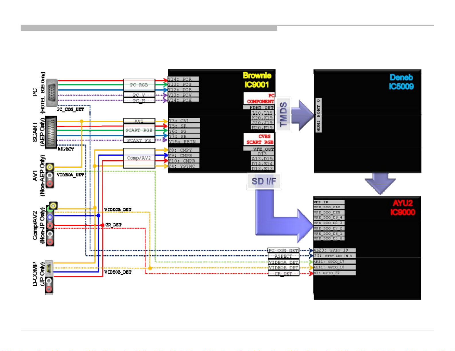
2.4 - RB2 ANALOG SIGNAL PATH
RB2G CHASSIS
W700B/ W800B
Troubleshooting
2-4. RB2 Analog Signal Path
Chassis: RB2G, HE-L
Chassis: RB2G, HE-L 76
Page 77
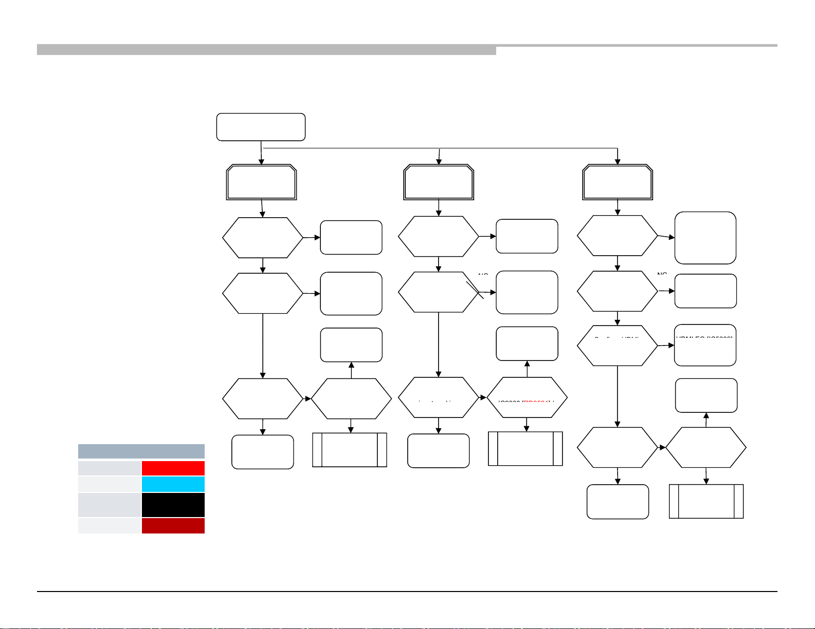
2.5-1 - NO PICTURE: (BAX + TUS)
RB2G CHASSIS
W700B/ W800B
Troubleshooting
No Picture GA
2-5-3. UC/GA/CH (BAX +TUS UC/GA/CH)
2-5. No Picture
Video 1
No Picture
Video 2
No Picture
Component
No Picture
OK
Check if input OSD
is GREY OUT
NG
Check J3104
Conn
VIDEOB_DET at
C8025 / C7026,
CR_DET at
C8014 / C7025
Check if input OSD
is GREY OUT
Check J3104
Connection,
VIDEOB_DET
At C8025 / C7026
OK
NG
Check if input OSD
is GREY OUT
Check J3101
connection,
VIDEOA_DET at
C8031 / C7030
OK
NG
NG
OK
Check wave
Between C3018/C3019
and IC9001
Detailed check
J3104 signal path
NG
OK
Check wave between
C3018 and IC9001
Detailed check
J3104 signal path
NG
Detailed SDIF path
OK
Check wave between
C3000 and IC9001
Detailed check
J3101 signal path
NG
Detailed SDIF path
HDMI EQ [IC5009]
Problem
Confi
rm
HDMI
input working
OK
Detailed TMDS path
check between
Confirm Analog RF
NG
Check between
IC9001 and IC9000
Check signal
between IC9001 and
NG
NG
Confirm Analog RF
NG
Check between
IC9001 and IC9000
Check signal
between IC9001 and
IC9001 and IC5009
Confirm other analog
Input working
NG
Check signal
between IC9001 and
IC5009 [RB5008]
NG
OK
i
nput working
IC9000 [
RB8524
] /
[R8570]
Ayu2 [IC9000]
Problem
OK
Brownie [IC9001]
Problem
OK
input working IC9000 [RB8524] /
[R8570]
Ayu2 [IC9000]
Problem
OK
Brownie [IC9001]
Problem
LEGEND
Ayu2 [IC9000]
Problem
OK
Brownie [IC9001]
Problem
OK
BAX
BAX-L
BAX & BAXL
TUS
/
TUW
85
For Atreyu(IC9000) replacement check page6
/
Chassis: RB2G, HE-L
Chassis: RB2G, HE-L 77
Page 78
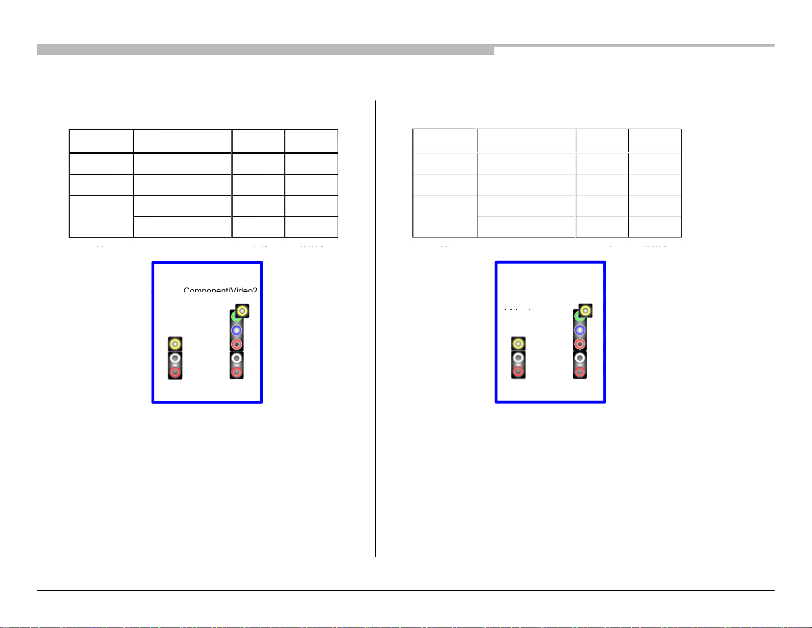
2.5-2 - NO PICTURE: INPUT SKIP FUNCTION - BAX/BAX-L
-
Non
Detect
Detect
Input Signal
Non
Detect
(Typical)
Detect
(Typical)
ビデオ
VIDEOA_DET(IC9000 K1)
" GPIO_47/DAUI_SPDIF_0 "
0V 3.3V
コンポーネント
VIDEOB_DET(IC9000 L3)
" GPIO_45/FE_PWMC”
3.3V 0V
PC
PC_CON_DET(IC9000 U25)
"
"
3.3V 0.07V
GPIO22
-
-
Non
Detect
(Typical)
Detect
(Typical)
VIDEOA_DET(IC9000 K1)
"GPIO_47/DAUI_SPDIF_0"
0V 3.3V
VIDEOB_DET(IC9000 L3)
" GPIO_45/FE_PWMC”
0V 3.3V
VIDEOB_DET [Y] (IC9000 L3)
" GPIO_45/FE_PWMC”
0V 3.3V
Input Signal
Non
Detect
(Typical)
Detect
(Typical)
ビデオ
VIDEOA_DET(IC9000 K1)
" GPIO_47/DAUI_SPDIF_0 "
0V 3.3V
コンポーネント
VIDEOB_DET(IC9000 L3)
" GPIO_45/FE_PWMC”
3.3V 0V
PC
PC_CON_DET(IC9000 U25)
"
"
3.3V 0.07V
CR_DET [Pr/Cr] (IC9000 M3)
" GPIO_34/FRAME_ID_2 "
0V 3.3V
PC_CON_DET(IC9000 U25)
"GPIO22"
3.3V 0.07V
GPIO22
ー
PC
PC
Component/Video2
ビデオ
コンポネント
Side Rear Side
Non-Detect
Detect
Input Signal
Non-Detect
(Typical)
Detect
(Typical)
Video1
VIDEOA_DET(IC9000
AA3
)
0V
3.3V
ビデオ
VIDEOA_DET(IC9000
AA3
)
" GPIO_47/DAUI_SPDIF_0 "
0V 3.3V
コンポーネント
VIDEOB_DET(IC9000 AD2)
" GPIO_45/FE_PWMC”
3.3V 0V
PC
PC_CON_DET(IC9000 U25)
"GPIO22"
3.3V 0.07V
Non-Detect
(Typical)
Detect
(Typical)
Input Signal
Non-Detect
(Typical)
Detect
(Typical)
1
VIDEOA_DET(IC9000
AA3
)
"GPIO_47/DAUI_SPDIF_0"
0V
3.3V
VIDEOB_DET(IC9000 AD2)
" GPIO_45/FE_PWMC”
0V 3.3V
VIDEOB_DET [Y] (IC9000 AD2)
" GPIO_45/FE_PWMC”
0V 3.3V
CR_DET [Pr/Cr] (IC9000 AA1)
"
GPIO_12/TIMER_CMPD/SPDIF_SEL
"
0V 3.3V
ビデオ
VIDEOA_DET(IC9000
AA3
)
" GPIO_47/DAUI_SPDIF_0 "
0V 3.3V
コンポーネント
VIDEOB_DET(IC9000 AD2)
" GPIO_45/FE_PWMC”
3.3V 0V
PC
PC_CON_DET(IC9000 U25)
"GPIO22"
3.3V 0.07V
PC_CON_DET(IC9000 U25)
"GPIO22"
3.3V 0.07V
C
C
コンポーネント
P
P
Video1
ビデオ
Side Rear Side
FOR BAX FOR BAX-L
Chassis: RB2G, HE-L
Input Signal
Video1
Video2
Component
(Y && Pr/Cr)
VIDEOA_DET(IC9000 K1)
"GPIO_47/DAUI_SPDIF_0"
VIDEOB_DET(IC9000 L3)
" GPIO_45/FE_PWMC”
VIDEOB_DET [Y] (IC9000 L3)
" GPIO_45/FE_PWMC”
CR_DET [Pr/Cr] (IC9000 M3)
" GPIO_34/FRAME_ID_2 "
PC_CON_DET(IC9000 U25)
Video1
-
(Typical)
0V 3.3V
0V 3.3V
0V 3.3V
0V 3.3V
Rear
(Typical)
Component
(Y && Pr/Cr)
Input Signal
"GPIO_47/DAUI_SPDIF_0"
Video2
VIDEOB_DET(IC9000 AD2)
" GPIO_45/FE_PWMC”
VIDEOB_DET [Y] (IC9000 AD2)
" GPIO_45/FE_PWMC”
CR_DET [Pr/Cr] (IC9000 AA1)
GPIO_12/TIMER_CMPD/SPDIF_SEL
PC_CON_DET(IC9000 U25)
"
"
Component/Video2
Rear
(Typical)
(Typical)
0V 3.3V
0V 3.3V
0V 3.3V
Chassis: RB2G, HE-L 78
Page 79
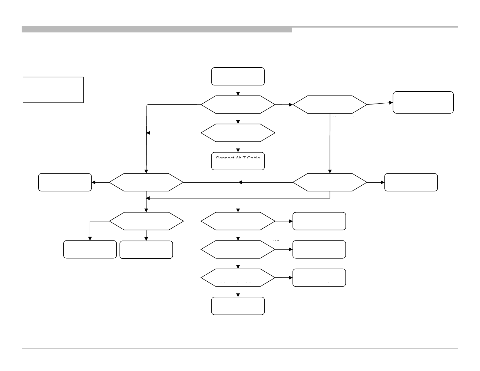
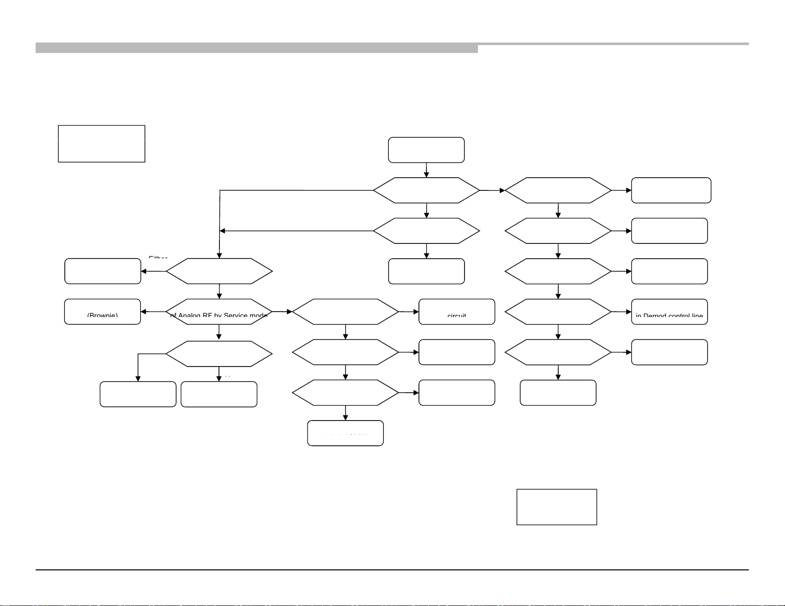
2.5-3 - NO PICTURE: TUNER
5. No Picture
Both
N
d
Connect ANT Cable
NG
IFOUTP1 / IFOUTN1
in IF1 line
Chassis: RB2G, HE-L
No Picture
Noisy Picture
Tuner
Check Brownie
Check M’t condition
RF Level =
in AGC1 line
High
Confirm RF Level and AGC
of Analog RF by Service mode
AGC = 0 AGC = 0
L
Confirm AGC1
IC2501 Pin6
H
Input signal is too big
Insert Attenuator
Which is NG?
Analog RF or Digital RF
OK
Confirm ANT connection
NG
correctly
RF Level = Low RF Level = Low
Confirm Power supply
for RF input circuit
A2.5V / LNA_5V
OK
Confirm tuner control line
TU_SCL / TU_SDA
A_RESET
OK
Confirm IF1 line
NG
NG
Sound is normal ?
o soun
Confirm RF Level and AGC
of Digital RF by Service mode
Check Power supply
circuit
Check M’t condition
in tuner control line
Check M’t condition
YesDigital onlyAnalog only
RF Level = High
Check IC9001(Brownie)/
IC9001(Ayu2)
Check Brownie
Chassis: RB2G, HE-L 79
OK
Check RF input circuit
include IC2501
Page 80
RB2G CHASSIS
W700B/ W800B
Troubleshooting
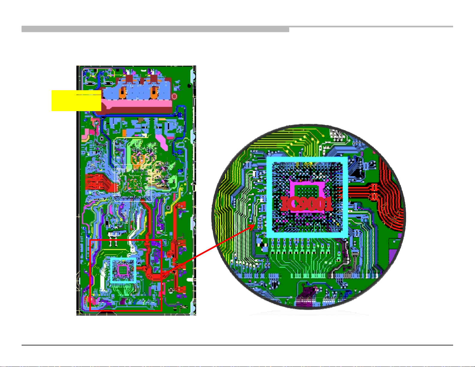
r
TUS BOARD
Tune
Chassis: RB2G, HE-L
IC9001
IC9001
Chassis: RB2G, HE-L 80
Page 81
RB2G CHASSIS
W700B/ W800B
Troubleshooting
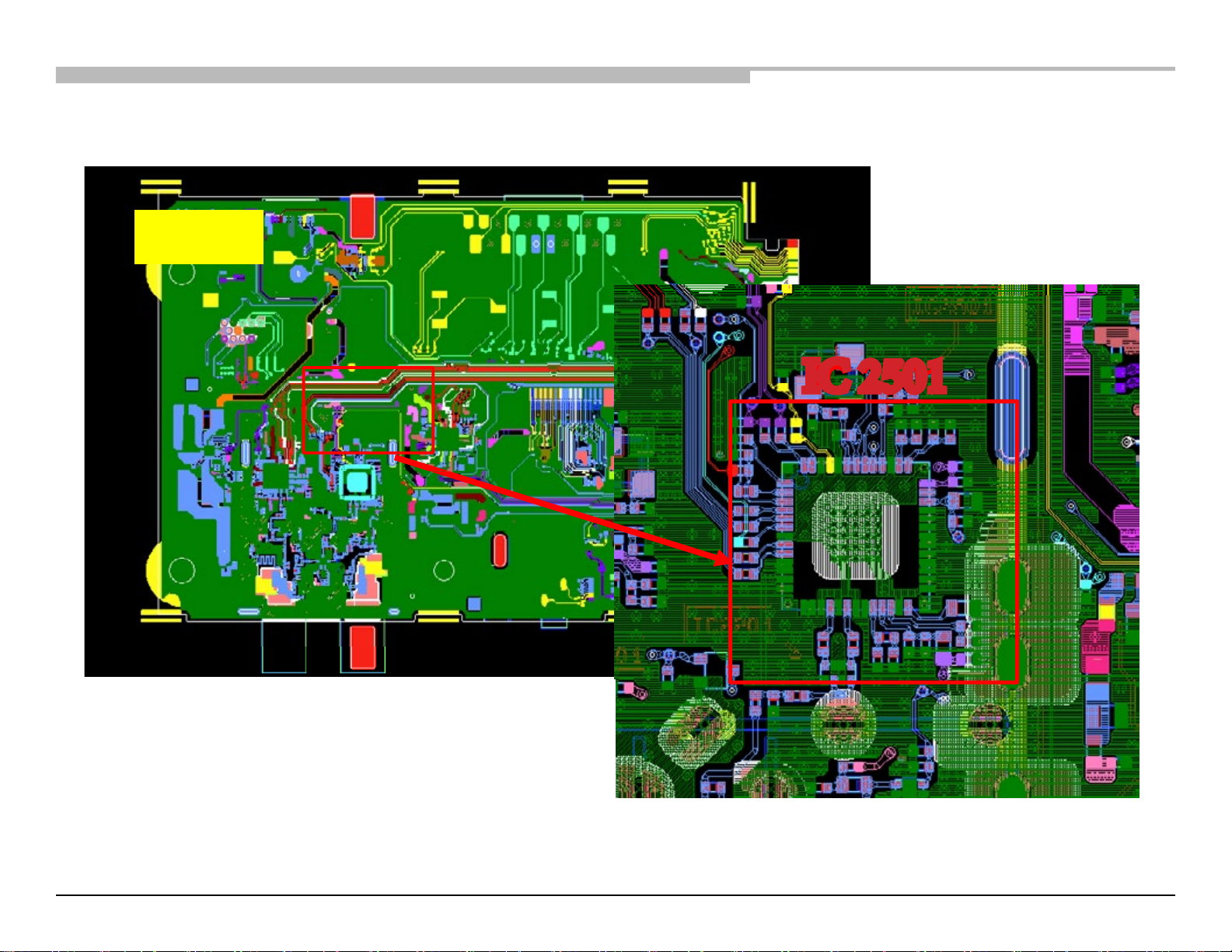
TUS BOARD
Tuner
IC 2501
97
TUS BOARD
Chassis: RB2G, HE-L
IC 2501
Chassis: RB2G, HE-L 81
Page 82
RB2G CHASSIS
W700B/ W800B
Troubleshooting
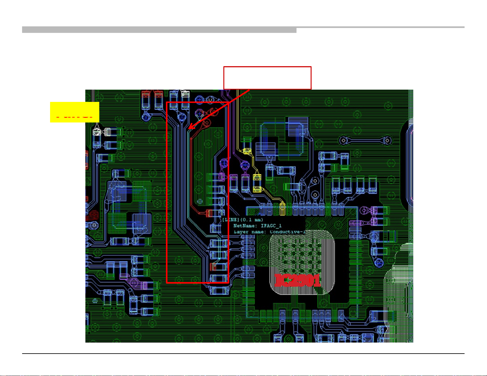
IFAGC_1
TUS BOARD
Tuner
IC2501
TUS BOARD
Chassis: RB2G, HE-L
Chassis: RB2G, HE-L 82
IC2501
Page 83
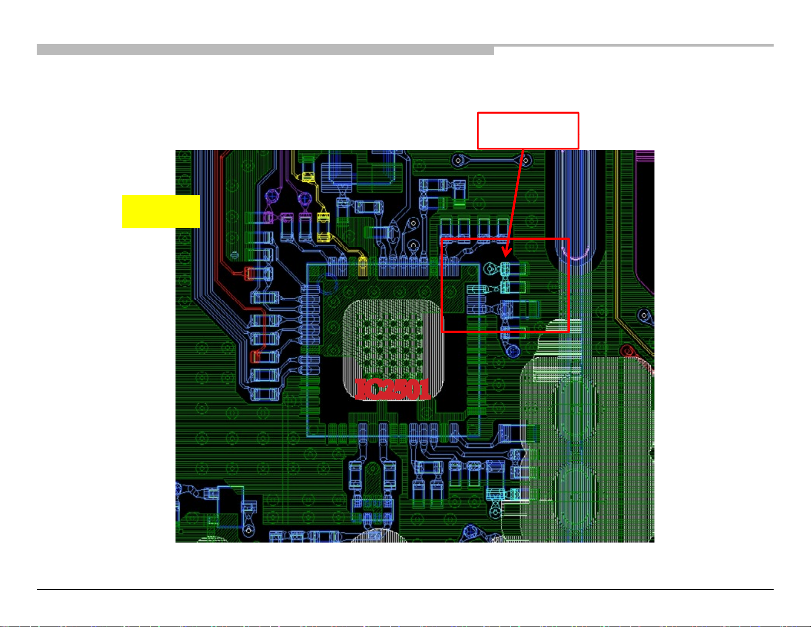
RB2G CHASSIS
W700B/ W800B
Troubleshooting
A2.5V
TUS BOARD
Tuner
IC2501
TUS BOARD
Chassis: RB2G, HE-L
Chassis: RB2G, HE-L 83
IC2501
Page 84
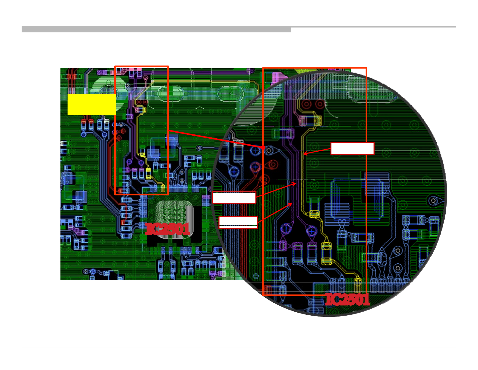
RB2G CHASSIS
W700B/ W800B
Troubleshooting
TUS BOARD
Tuner
A_RESET
TU SCL
TU_SDA
IC2501
_
IC2501
TUS BOARD
Chassis: RB2G, HE-L
Chassis: RB2G, HE-L 84
IC2501
IC2501
Page 85
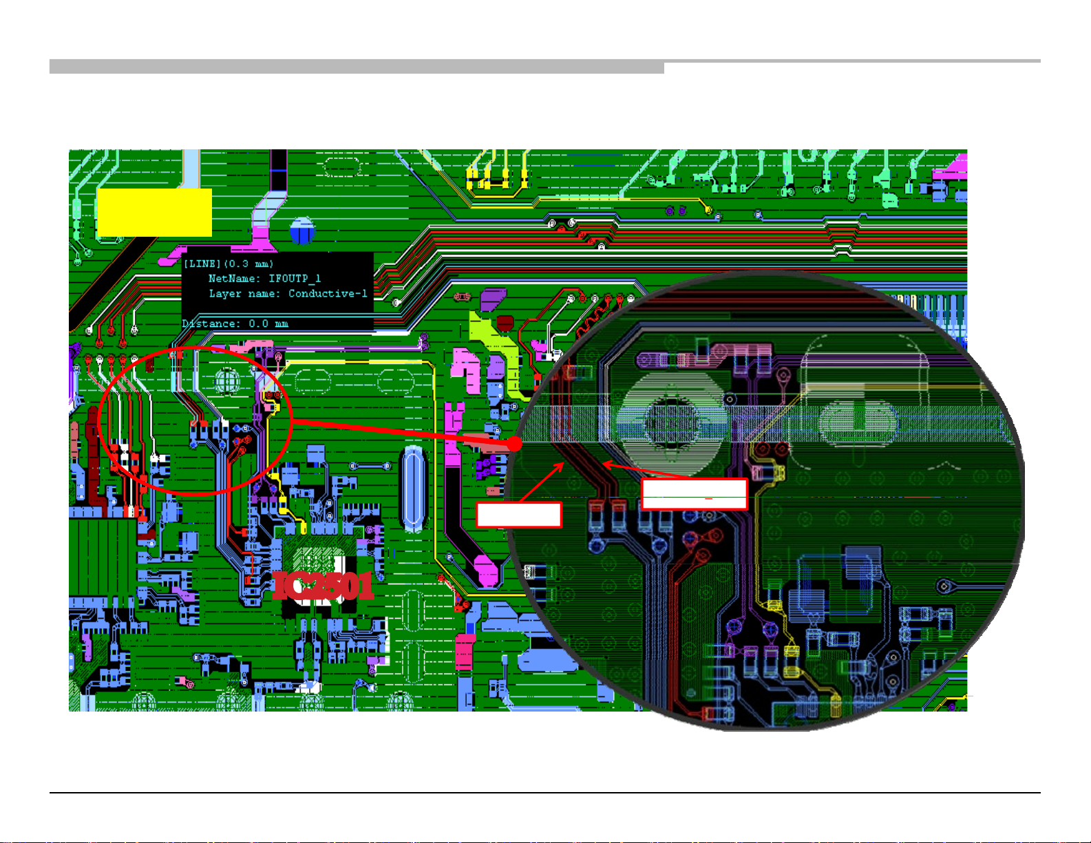
RB2G CHASSIS
W700B/ W800B
Troubleshooting
TUS BOARD
_
TUS BOARD
Tuner
Chassis: RB2G, HE-L
Chassis: RB2G, HE-L 85
IC2501
IC2501
IFOUTN 1
IFOUTP_1
Page 86
2.5-4. TUNER COL-T2 / BRZ / ARG
RB2G CHASSIS
W700B/ W800B
Troubleshooting
2-5-10. Tuner COL-T2 / BRZ / ARG
2-5. No Picture
No Picture
Noisy Picture
Which is NG?
Analog RF or Digital RF
Sound is normal ?
Check IC9001(Brownie)/
IC9001(Ayu2)
YesDigital onlyAnalog only
Tuner
Both
Confirm ANT connection
OK
No sound
NG NG
Error free
Confirm BER of digital RF
By Service mode
Check Brownie and
M’t condition in TS line
Connect ANT Cable
correctly
Confirm Power supply
for RF input circuit
Confirm RF Level and AGC
Check IC9001
Check Power supply
NG
Confirm Power supply
for Digital Demod
DDEM1.1V / DDEM3.3V
Confirm Demod control line
I2CB_SCL / I2CB_SDA
OK
Check Power supply
circuit
Check M’t condition
NG
NG
RF Level=High
AGC=Low
RF Level =Low
AGC=High
Which is NG?
Terrestrial or Cable
Both
Check IC2501
Either
A2.5V / LNA_5V
of Analog RF by Service mode
(Brownie)
Confirm tuner control line
TU_SCL / TU_SDA
A_RESET
OK
OK
circuit
Check M’t condition
in tuner control line
NG
AGC = 0
DMD_RESET / OSC_ENBN-1
OK
in Demod control line
Check M’t condition
in AGC2/IF2 line
Confirm RF Level and AGC
of Digital RF by Service mode
AGC=Low
AGC=High,
L
Confirm AGC1
IC2151 Pin6
Check RF input circuit
Confirm IF1 line
IFOUTP1 / IFOUTN1
OK
Check M’t condition
in IF1 line
NG
Check IC2201
Check M’t condition
in AGC1 line
Input signal is too big
Set LNA off
H
include IC2501
Note:
(AYU2) – IC9000
(Brownie)- IC9001
Chassis: RB2G, HE-L
Chassis: RB2G, HE-L 86
Page 87
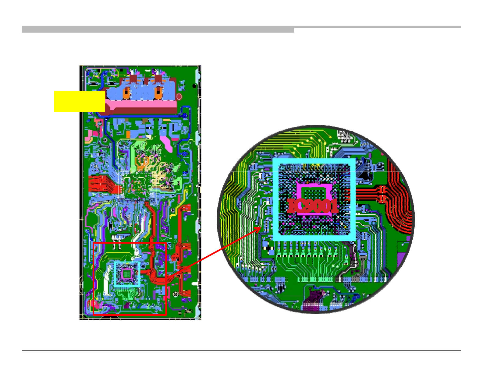
RB2G CHASSIS
W700B/ W800B
Troubleshooting
BAX BOARD – IC9001 (BROWNIE)
Tuner
IC9001
BAX BOARD - IC9001 (BROWNIE)
Chassis: RB2G, HE-L
IC9001
Chassis: RB2G, HE-L 87
Page 88
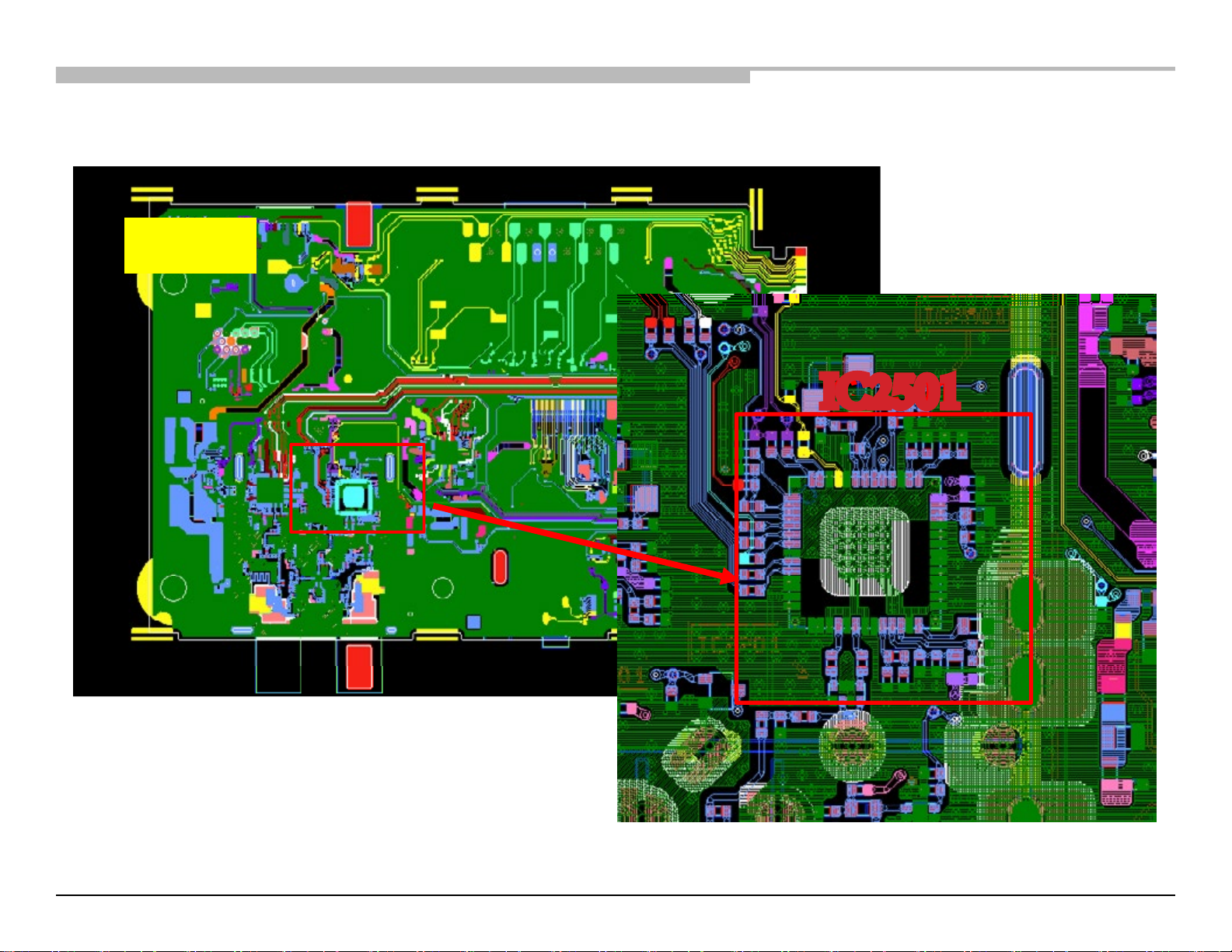
RB2G CHASSIS
W700B/ W800B
Troubleshooting
TUS BOARD – IC2501
Tuner
IC 2501
TUS BOARD - IC2501
Chassis: RB2G, HE-L
IC2501
Chassis: RB2G, HE-L 88
Page 89
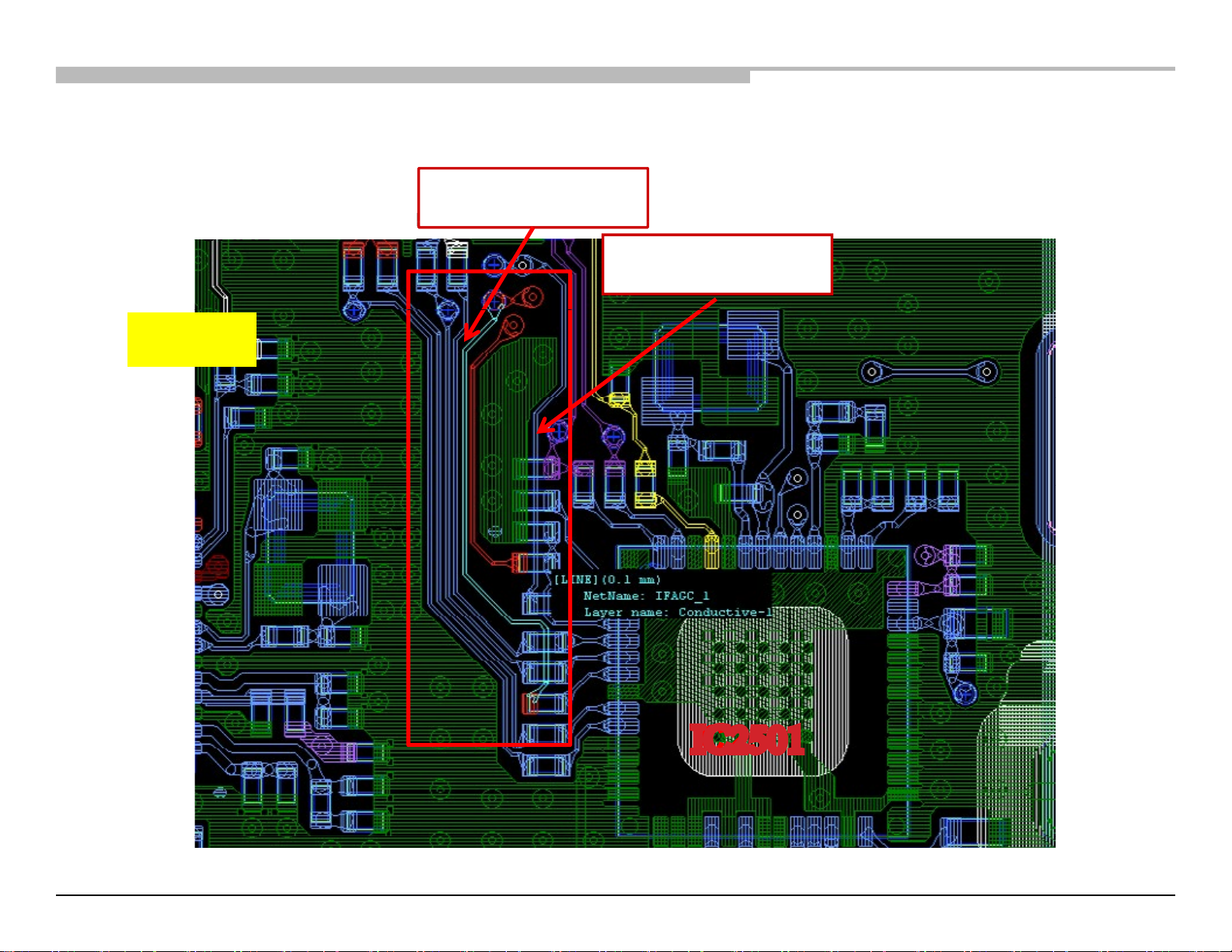
RB2G CHASSIS
W700B/ W800B
Troubleshooting
IFAGC_1
IFAGC_2
Tuner
IC2501
TUS BOARD
Chassis: RB2G, HE-L
Chassis: RB2G, HE-L 89
IC2501
Page 90
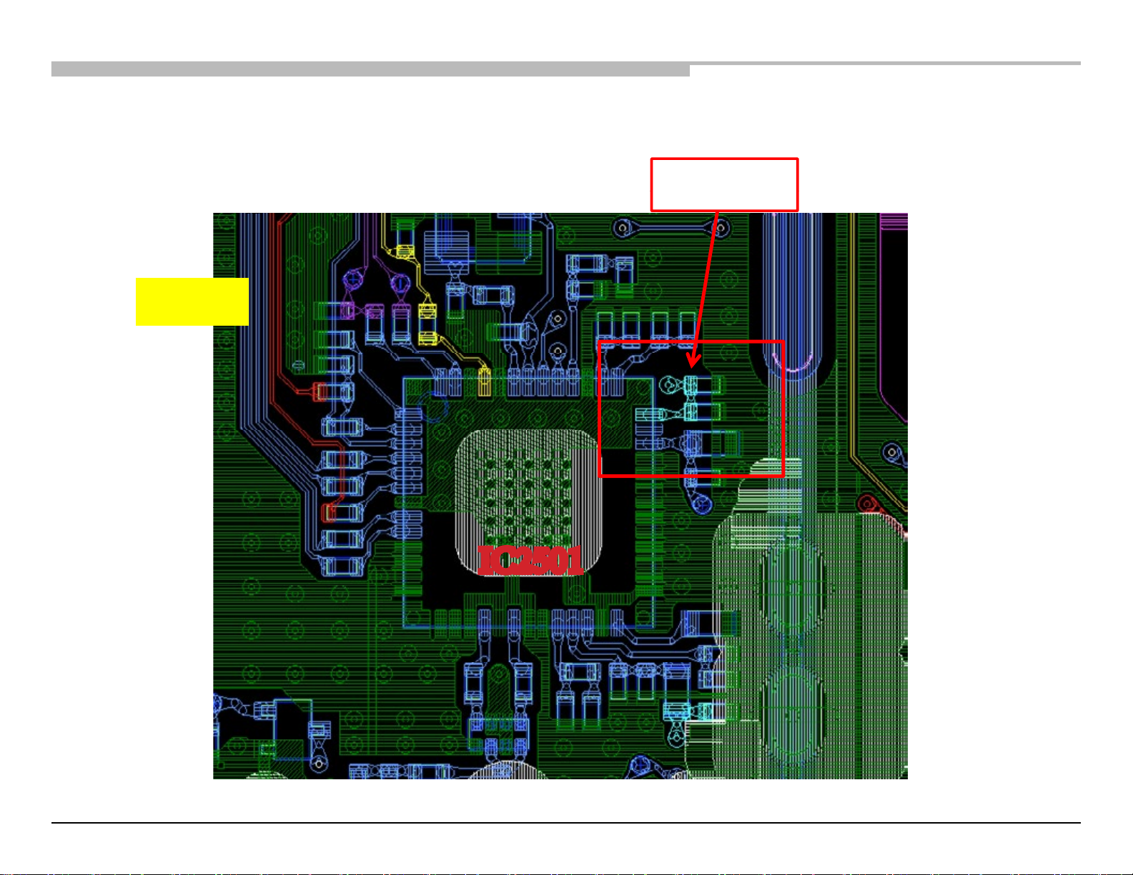
RB2G CHASSIS
W700B/ W800B
Troubleshooting
A2.5V
Tuner
IC2501
TUS BOARD
Chassis: RB2G, HE-L
IC2501
Chassis: RB2G, HE-L 90
Page 91
RB2G CHASSIS
W700B/ W800B
Troubleshooting
TUS BOARD
Tuner
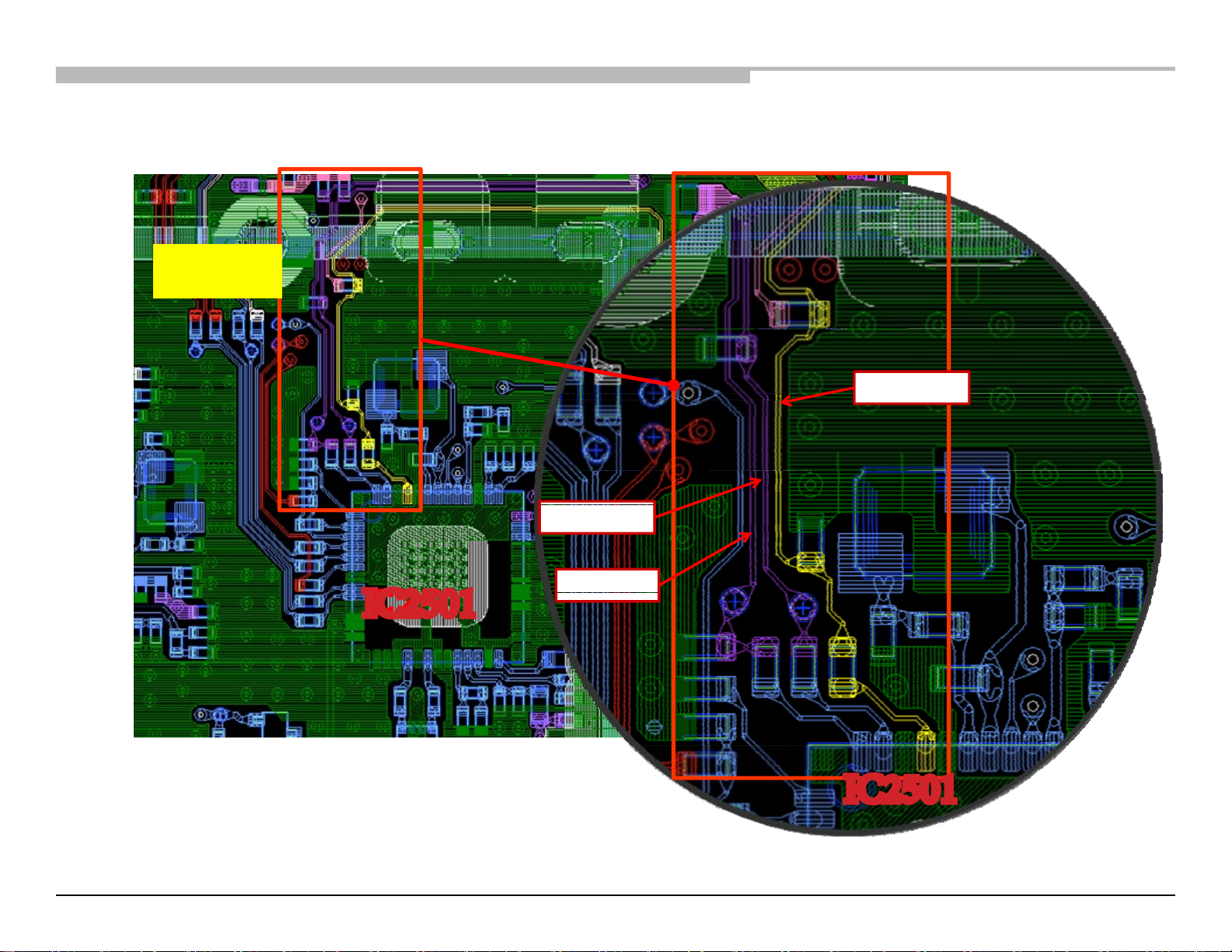
A_RESET
TU SCL
TU_SDA
IC2501
_
IC2501
TUS BOARD
Chassis: RB2G, HE-L
Chassis: RB2G, HE-L 91
IC2501
IC2501
Page 92
RB2G CHASSIS
W700B/ W800B
Troubleshooting
TUS BOARD
Tuner
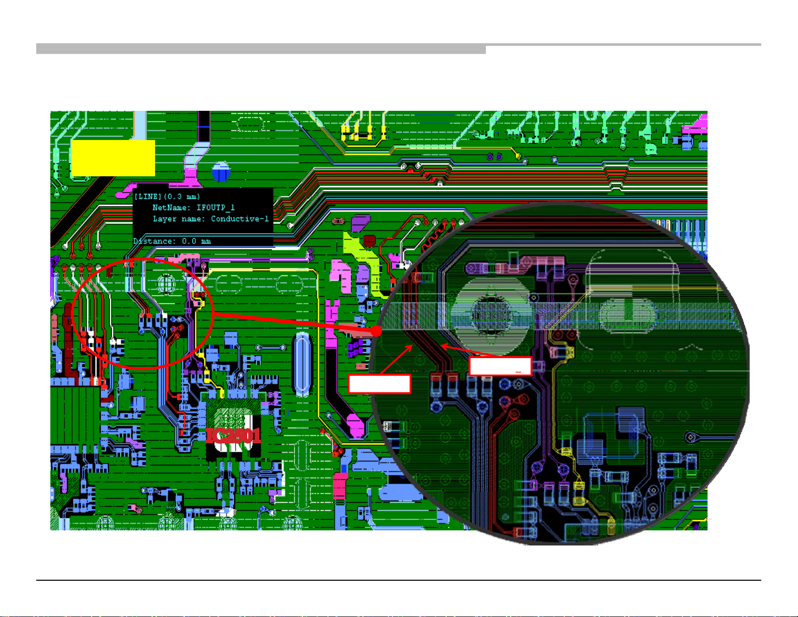
IFOUTN
IFOUTP_1
_
1
IC2501
TUS BOARD
Chassis: RB2G, HE-L
IC2501
Chassis: RB2G, HE-L 92
Page 93
RB2G CHASSIS
W700B/ W800B
Troubleshooting
TUS BOARD
Tuner
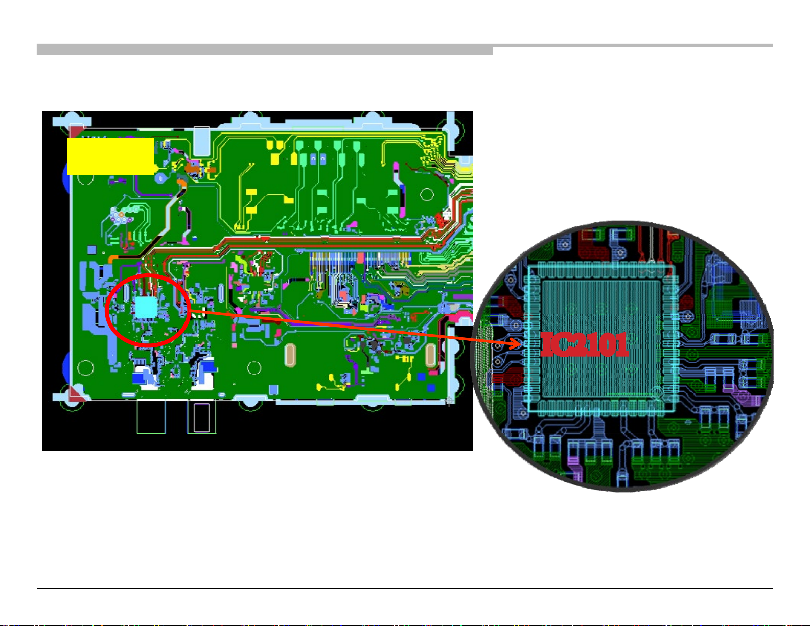
IC2101
TUS BOARD
Chassis: RB2G, HE-L
IC2101
Chassis: RB2G, HE-L 93
Page 94
RB2G CHASSIS
W700B/ W800B
Troubleshooting
TUS BOARD
Tuner
TUS BOARD
Chassis: RB2G, HE-L
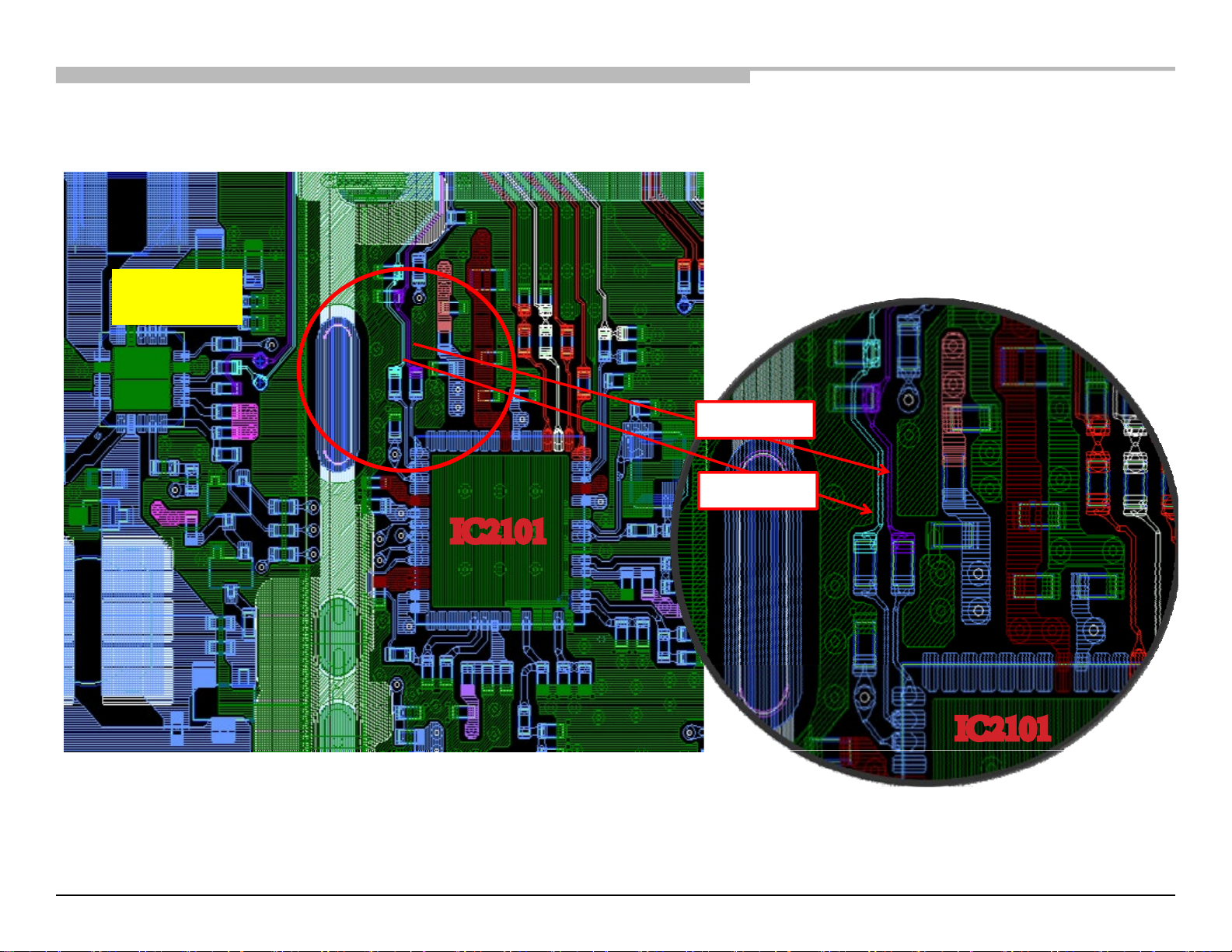
I2CB_SCL
Chassis: RB2G, HE-L 94
IC2101
IC2101
I2CB_SDA
IC2101
IC2101
Page 95
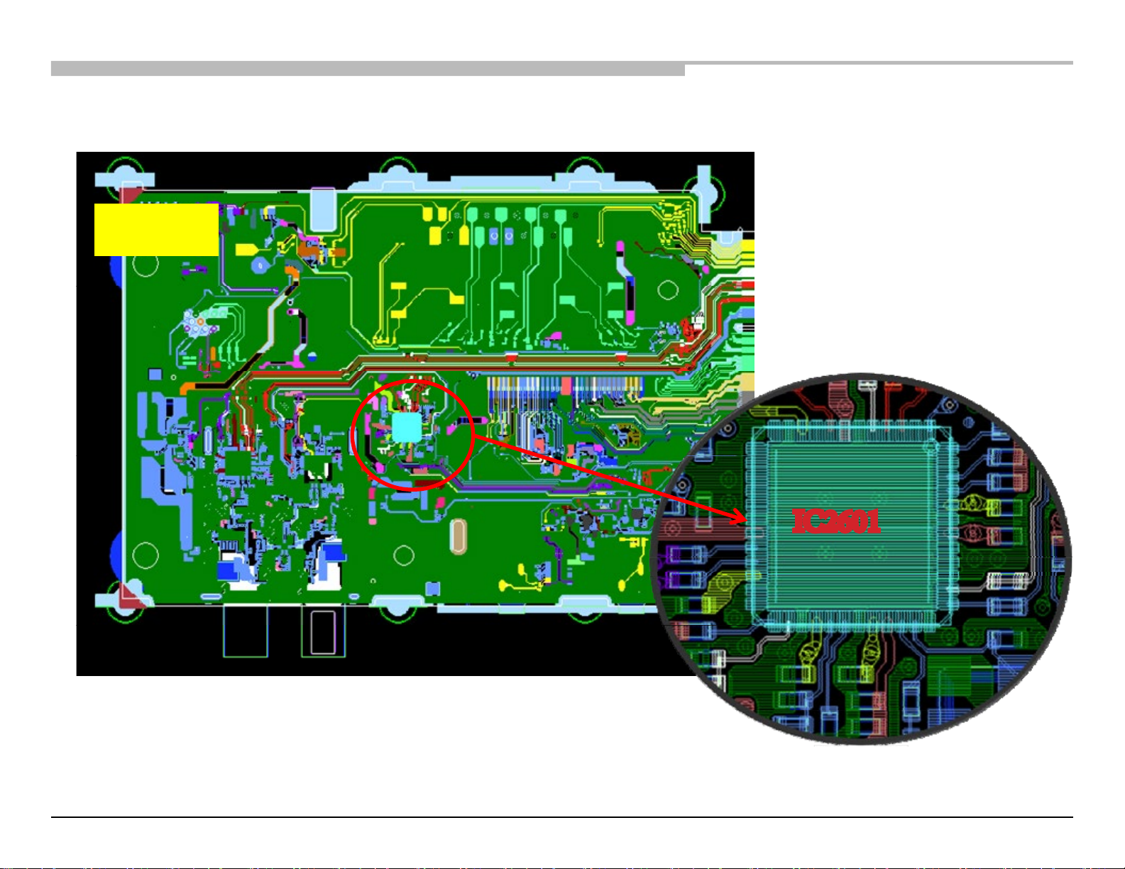
RB2G CHASSIS
W700B/ W800B
Troubleshooting
TUS BOARD
TUS BOARD
Tuner
Chassis: RB2G, HE-L
IC2601
IC2601
Chassis: RB2G, HE-L 95
Page 96
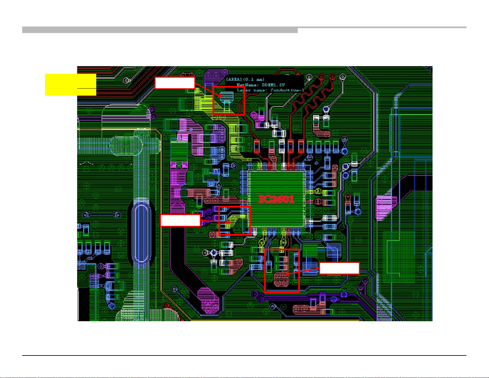
RB2G CHASSIS
W700B/ W800B
Troubleshooting
DDEM1.2V
TUS BOARD
Tuner
IC2601
DDEM1.1V
DDEM3.3V
TUS BOARD
Chassis: RB2G, HE-L
Chassis: RB2G, HE-L 96
IC2601
Page 97
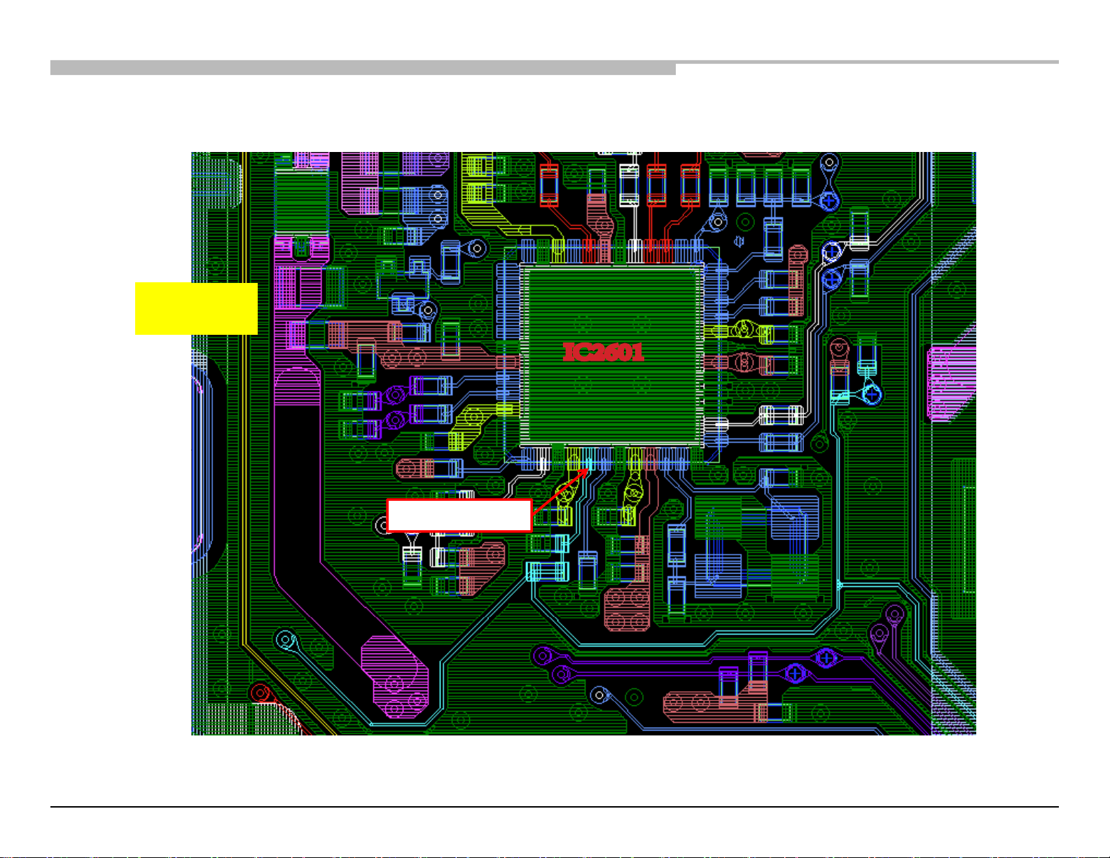
RB2G CHASSIS
W700B/ W800B
Troubleshooting
TUS BOARD
TUS BOARD
Tuner
IC2601
IC2601
Chassis: RB2G, HE-L
DMD_RESET1
Chassis: RB2G, HE-L 97
Page 98
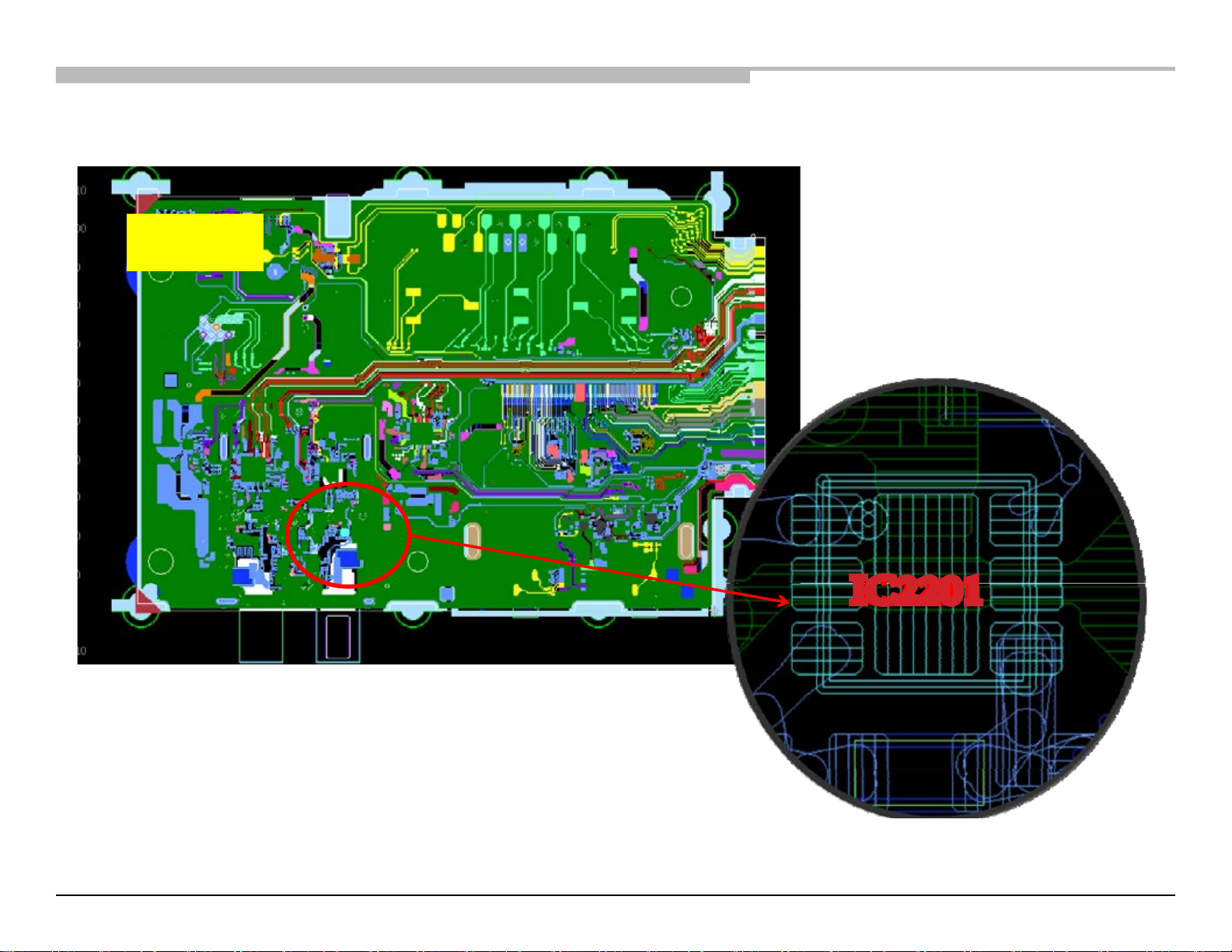
RB2G CHASSIS
W700B/ W800B
Troubleshooting
TUS BOARD
IC2201
TUS BOARD
Tuner
Chassis: RB2G, HE-L
Chassis: RB2G, HE-L 98
IC2201
1
Page 99
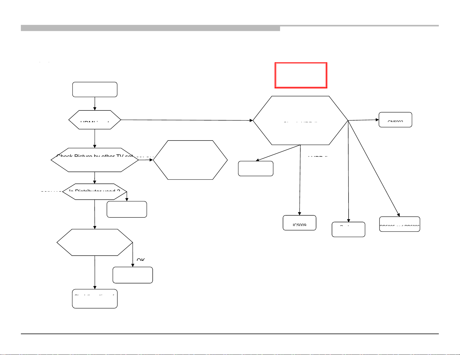
2.5-5 - NO PICTURE: HDMI
RB2G CHASSIS
W700B/ W800B
Troubleshooting
2-5-13. HDMI
2-5. No Picture
No Pict
HDMI i
t
HPD
CN5002
Check Picture by other TV set
HPD li
set OK
both NG
Is Distributor used ?
IC5009
Repl
RB5005
and RB5006
OK
Check th
tti
Chassis: RB2G, HE-L
Target board &
other TV set
ure
Check other
npu
All Inputs
are NG
which is same model
Connect Source
NO
Check Source equipment
by Reference TV set
(For example, RB1)
equipment directly
Other TV
Check IC5009 All power
(Refer to next page)
YES
Reference TV Set
Other Input is OK
Supply pin
Only +5V line
is NG
Replace
R5105
For example,
Only HDMI 4 is
NG
Check the below point at
IC5009 side
・Check +5V line
・Check
line
・Check DDC lines
・Check TMDS lines
+5V line is OK
and
is NG
Replace
ne
All lines
are NG
Only DDC lines
are NG
ace
RB5016
Replace
Only TMDS lines
are NG
Replace
Reference TV set
Chassis: RB2G, HE-L 99
NG
e se
Source equipment
ngs of
Inform the designer
of it
Page 100
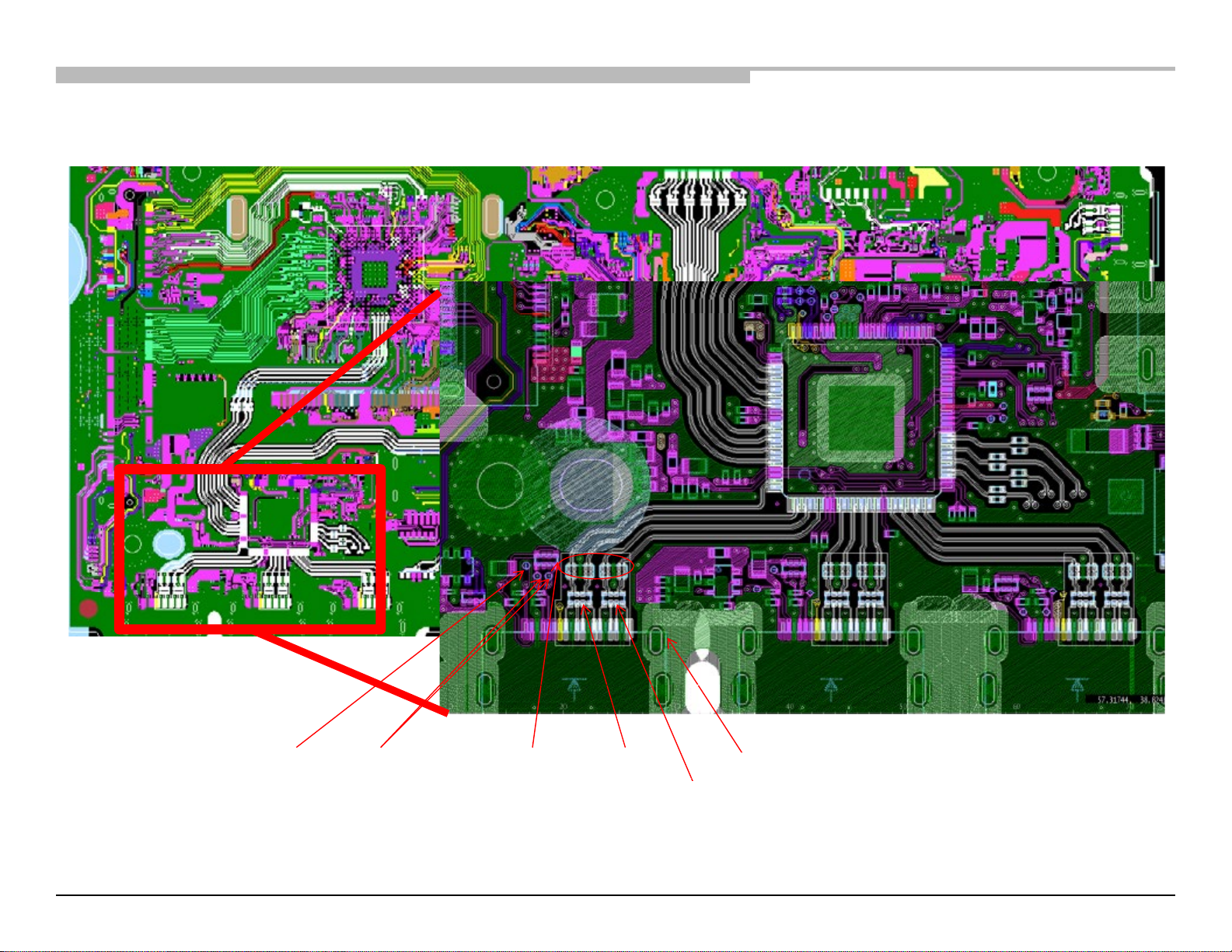
RB2G CHASSIS
W700B/ W800B
Troubleshooting
TMDS
RB5016
RB5005 CN5002HPD DDC
RB5006
BAXLBAXL--A SideA Side
BAX-L BOARD (Side A)
Chassis: RB2G, HE-L
HPD
DDC
RB5016
RB5005
CN5002
RB5006
Chassis: RB2G, HE-L 100
 Loading...