

Page 1

HISTORY INFORMATION FOR THE FOLLOWING MANUAL:
SERVICE MANUAL
MODEL NAME REMOTE COMMANDER DESTINATION
KDL-32FA600
KDL-32FA600
RM-YD035 MX
RM-YD035 LATIN AMERICA
AZ1-K
CHASSIS
LEVEL
CONFIDENTIAL
3
CONFIDENTIAL
ELECTRICAL SERVICE MANUAL
INTERNAL ONLY
ORIGINAL MANUAL ISSUE DATE: 2/2010
REVISION DATE SUBJECT
2/2010 No revisions or updates are applicable at this time.
9-883-847-51
LCD DIGITAL COLOR TV
Page 2

KDL-32FA600
TABLE OF CONTENTS
SECTION TITLE PAGE
Safety-Related Component Warning ..........................................................................................................................................................................3
Safety Check-Out ....................................................................................................................................................................................................... 5
SECTION 1: DIAGRAMS ................................................................................................................................................................................................... 6
1-1. Circuit Boards Location ...................................................................................................................................................................................... 6
1-2. Printed Wiring Boards and Schematic Diagrams Information ............................................................................................................................ 6
1-3. Block Diagrams ................................................................................................................................................................................................. 8
1-4. Schematics and Supporting Information ............................................................................................................................................................9
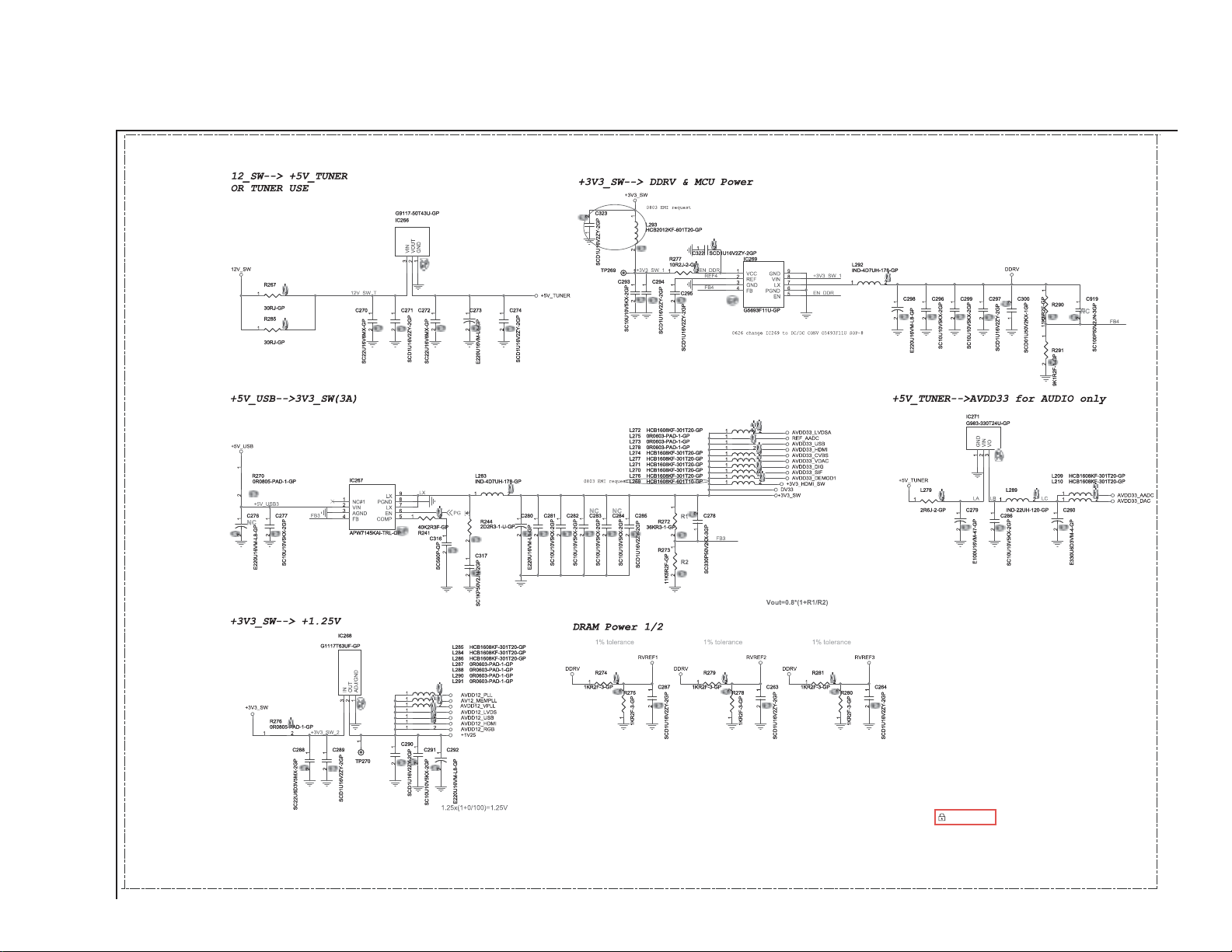
A Board Schematic Diagram (1 of 20) ................................................................................................................................................................ 9
A Board Schematic Diagram (2 of 20) .............................................................................................................................................................. 10
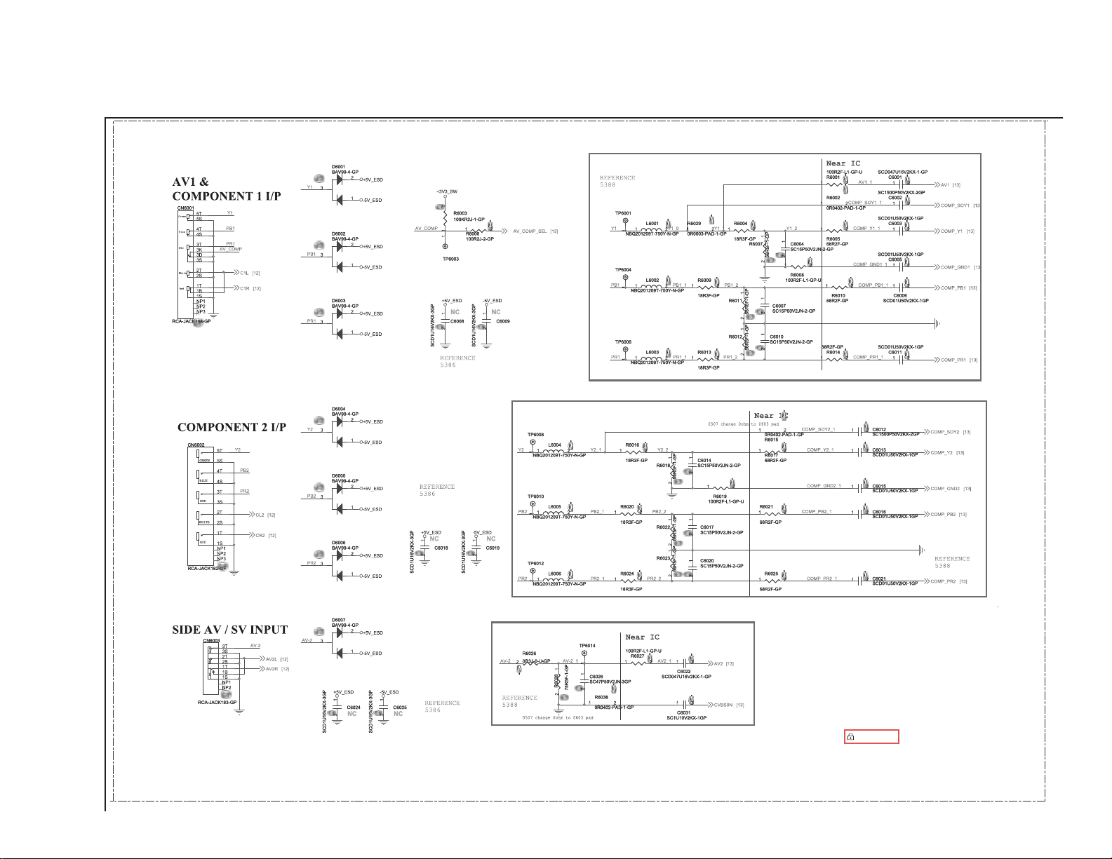
A Board Schematic Diagram (3 of 20) .............................................................................................................................................................. 11
A Board Schematic Diagram (4 of 20) .............................................................................................................................................................. 12
A Board Schematic Diagram (5 of 20) .............................................................................................................................................................. 13
A Board Schematic Diagram (6 of 20) .............................................................................................................................................................. 14
A Board Schematic Diagram (7 of 20) .............................................................................................................................................................. 15
A Board Schematic Diagram (8 of 20) .............................................................................................................................................................. 16
A Board Schematic Diagram (9 of 20) .............................................................................................................................................................. 17
A Board Schematic Diagram (10 of 20) ............................................................................................................................................................ 18
A Board Schematic Diagram (11 of 20) ............................................................................................................................................................ 19
A Board Schematic Diagram (12 of 20) ............................................................................................................................................................ 20
A Board Schematic Diagram (13 of 20) ............................................................................................................................................................ 21
A Board Schematic Diagram (14 of 20) ............................................................................................................................................................ 22
A Board Schematic Diagram (15 of 20) ............................................................................................................................................................ 23
A Board Schematic Diagram (16 of 20) ............................................................................................................................................................ 24
A Board Schematic Diagram (17 of 20) ............................................................................................................................................................ 25
A Board Schematic Diagram (18 of 20) ............................................................................................................................................................ 26
A Board Schematic Diagram (19 of 20) ............................................................................................................................................................ 27
A Board Schematic Diagram (20 of 20) ............................................................................................................................................................ 28
G2HE Board Schematic Diagram ....................................................................................................................................................................31
H2 Board Schematic Diagram .......................................................................................................................................................................... 34
KD Board Schematic Diagram (1 of 2) .............................................................................................................................................................35
KD Board Schematic Diagram (2 of 2) .............................................................................................................................................................36
APPENDIX A: ENCRYPTION KEY COMPONENTS ..................................................................................................................................................... A-1
KDL-32FA600
2
Page 3
SAFETY-RELATED COMPONENT WARNING
KDL-32FA600
There are critical components used in LCD color TVs that are important for safety. These components are identifi ed with shading and
mark on the schematic diagrams and the electrical parts list. It is essential that these critical parts be replaced only with the part number
specifi ed in the electrical parts list to prevent electric shock, fi re, or other hazard.
NOTE: Do not modify the original design without obtaining written permission from the manufacturer or you will void the original parts and
labor guarantee.
!
USE CAUTION WHEN HANDLING THE LCD PANEL
When repairing the LCD panel, be sure you are grounded by using a wrist band.
When installing the LCD panel on a wall, the LCD panel must be secured using the 4 mounting holes on the rear cover.
To avoid damaging the LCD panel:
do not press on the panel or frame edge to avoid the risk of electric shock.
do not scratch or press on the panel with any sharp objects.
do not leave the module in high temperatures or in areas of high humidity for an extended period of time.
do not expose the LCD panel to direct sunlight.
avoid contact with water. It may cause a short circuit within the module.
disconnect the AC adapter when replacing the backlight (CCFL) or inverter circuit.
(High voltage occurs at the inverter circuit at 650Vrms.)
always clean the LCD panel with a soft cloth material.
use care when handling the wires or connectors of the inverter circuit. Damaging the wires may cause a short.
protect the panel from ESD to avoid damaging the electronic circuit (C-MOS).
LEAKAGE CURRENT HOT CHECK CIRCUIT
KDL-32FA600
3
Page 4
The circuit boards used in these models have been processed using
Lead Free Solder. The boards are identified by the LF logo located
close to the board designation e.g. H1 etc [ see example ]. The
servicing of these boards requires special precautions to be taken as
outlined below.
example
It is strongly recommended to use Lead Free Solder material in order to guarantee optimal quality of new solder joints.
Lead Free Solder is available under the following part numbers :
KDL-32FA600
r e b m u n t r a P r e t e m a i D s k r a m e R
9 1 - 5 0 0 - 0 4 6 - 7m m 3 . 0g K 5 2 . 0
0 2 - 5 0 0 - 0 4 6 - 7m m 4 . 0g K 0 5 . 0
1 2 - 5 0 0 - 0 4 6 - 7m m 5 . 0g K 0 5 . 0
2 2 - 5 0 0 - 0 4 6 - 7m m 6 . 0g K 5 2 . 0
3 2 - 5 0 0 - 0 4 6 - 7m m 8 . 0g K 0 0 . 1
4 2 - 5 0 0 - 0 4 6 - 7m m 0 . 1g K 0 0 . 1
5 2 - 5 0 0 - 0 4 6 - 7m m 2 . 1g K 0 0 . 1
6 2 - 5 0 0 - 0 4 6 - 7m m 6 . 1g K 0 0 . 1
Due to the higher melting point of Lead Free Solder the soldering iron tip temperature needs to be set to 370 degrees centigrade.
This requires soldering equipment capable of accurate temperature control coupled with a good heat recovery characteristics.
For more information on the use of Lead Free Solder, please refer to
http://www.sony-training.com
KDL-32FA600
4
Page 5
SAFETY CHECK-OUT
To E
l
KDL-32FA600
After correcting the original service problem, perform the following
safety checks before releasing the set to the customer:
1. Check the area of your repair for unsoldered or poorly soldered
connections. Check the entire board surface for solder splashes and
bridges.
2. Check the interboard wiring to ensure that no wires are “pinched” or
touching high-wattage resistors.
3. Check that all control knobs, shields, covers, ground straps, and
mounting hardware have been replaced. Be absolutely certain that
you have replaced all the insulators.
4. Look for unauthorized replacement parts, particularly transistors,
that were installed during a previous repair. Point them out to the
customer and recommend their replacement.
5. Look for parts which, though functioning, show obvious signs of
deterioration. Point them out to the customer and recommend their
replacement.
6. Check the line cords for cracks and abrasion. Recommend the
replacement of any such line cord to the customer.
7. Check the antenna terminals, metal trim, “metallized” knobs, screws,
and all other exposed metal parts for AC leakage. Check leakage as
described below.
The AC leakage from any exposed metal part to earth ground and
from all exposed metal parts to any exposed metal part having a
return to chassis, must not exceed 0.5 mA (500 microamperes).
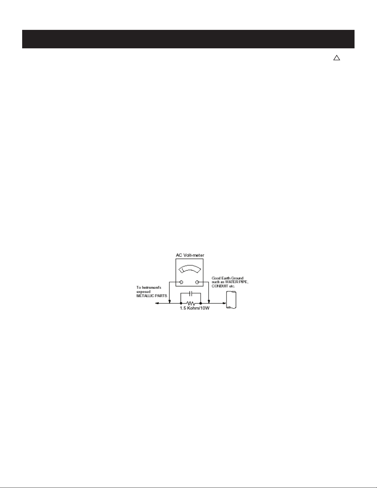
Leakage current can be measured by any one of three methods.
1. A commercial leakage tester, such as the Simpson 229 or RCA
WT-540A. Follow the manufacturers’ instructions to use these
instructions.
2. A battery-operated AC milliampmeter. The Data Precision 245
digital multimeter is suitable for this job.
3. Measuring the voltage drop across a resistor by means of a VOM
or battery-operated AC voltmeter. The “limit” indication is 0.75
V, so analog meters must have an accurate low voltage scale.
The Simpson’s 250 and Sanwa SH-63TRD are examples of
passive VOMs that are suitable. Nearly all battery-operated digital
multimeters that have a 2 VAC range are suitable (see Figure A).
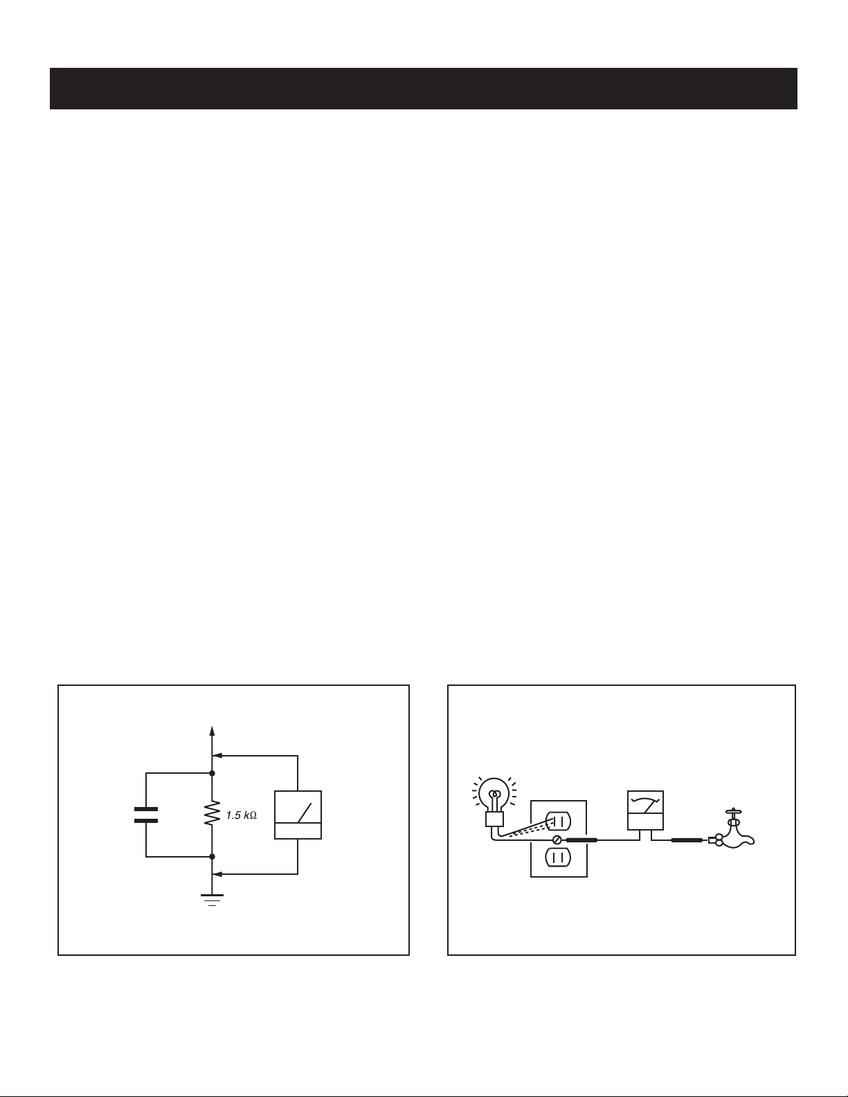
How to Find a Good Earth Ground
A cold-water pipe is a guaranteed earth ground; the cover-plate
retaining screw on most AC outlet boxes is also at earth ground. If the
retaining screw is to be used as your earth ground, verify that it is at
ground by measuring the resistance between it and a cold-water pipe
with an ohmmeter. The reading should be zero ohms.
If a cold-water pipe is not accessible, connect a 60- to 100-watt
trouble- light (not a neon lamp) between the hot side of the receptacle
and the retaining screw. Try both slots, if necessary, to locate the hot
side on the line; the lamp should light at normal brilliance if the screw
is at ground potential (see Figure B).
Leakage Test
0.15 μF
Figure A. Using an AC voltmeter to check AC leakage. Figure B. Checking for earth ground.
xposed Meta
Parts on Set
Earth Ground
AC
Voltmeter
(0.75V)
Trouble Light
AC Outlet Box
Ohmmeter
Cold-water Pipe
KDL-32FA600
5
Page 6
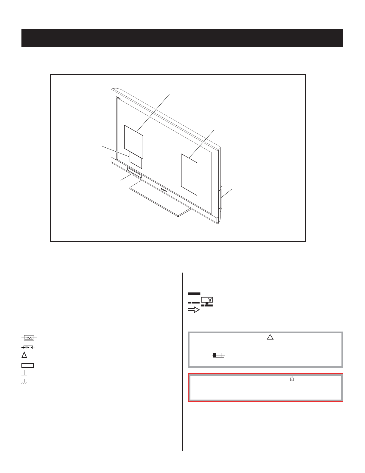
1-1. CIRCUIT BOARDS LOCATION
KD
H2
KDL-32FA600
SECTION 1: DIAGRAMS
A
G2HE
SWITCH UNIT
1-2.
PRINTED WIRING BOARDS AND SCHEMATIC DIAGRAMS INFORMATION
All capacitors are in μF unless otherwise noted. pF : μμF 50WV or
less are not indicated except for electrolytics and tantalums.
All electrolytics are in 50V unless otherwise specifi ed.
All resistors are in ohms. k=1000, M=1000k
Indication of resistance, which does not have one for rating
electrical power, is as follows: Pitch : 5mm
Rating electrical power :
1
/
W in resistance, 1/
4
W and 1/
10
W in chip resistance.
16
1
/
4
: nonfl ammable resistor
: fusible resistor
: internal component
: panel designation and adjustment for repair
All voltages are in V.
S : Measurement impossibility.
: B+line.
: B-line. (Actual measured value may be different).
: signal path. (RF)
Circled numbers are waveform references.
W
The components identifi ed by shading and ! symbol are critical for safety. Replace
only with part number specifi ed.
The symbol indicates a fast operating fuse and is displayed on the component
side of the board. Replace only with fuse of the same rating as marked.
: earth ground
: earth-chassis
All variable and adjustable resistors have characteristic curve B,
unless otherwise noted.
NOTE: The components identifi ed by a red outline and a mark contain confi dential
information. Specifi c instructions must be adhered to whenever these components
are repaired and/or replaced.
See Appendix A: Encryption Key Components in the back of this manual.
Readings are taken with a color-bar signal input.
Readings are taken with a 10M digital multimeter.
Voltages are DC with respect to ground unless otherwise noted.
Voltage variations may be noted due to normal production
tolerances.
KDL-32FA600
6
Page 7
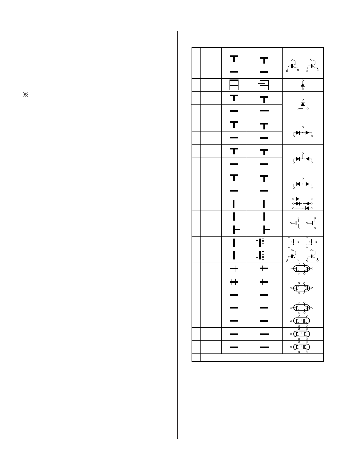
KDL-32FA600
REFERENCE INFORMATION
RESISTOR
: RN METAL FILM
: RC SOLID
: FPRD NONFLAMMABLE CARBON
: FUSE NONFLAMMABLE FUSIBLE
: RW NONFLAMMABLE WIREWOUND
: RS NONFLAMMABLE METAL OXIDE
: RB NONFLAMMABLE CEMENT
: ADJUSTMENT RESISTOR
COIL
: LF-8L MICRO INDUCTOR
CAPACITOR
: TA TANTALUM
: PS STYROL
: PP POLYPROPYLENE
: PT MYLAR
: MPS METALIZED POLYESTER
: MPP METALIZED POLYPROPYLENE
: ALB BIPOLAR
: ALT HIGH TEMPERATURE
: ALR HIGH RIPPLE
Terminal name of semiconductors in silk screen
printed circuit ( )
Device Printed symbol Terminal name
Transistor
1
Transistor
2
3
Diode
4
Diode
Diode
5
Diode
6
Diode
7
8
Diode
Diode
9
Diode
10
Diode
11
Diode
12
Transistor
13
(FET)
Transistor
14
(FET)
Transistor
15
(FET)
Transistor
16
Transistor
17
Transistor
18
Transistor
19
Transistor
20
Transistor
21
Transistor
22
Transistor
23
Discrete semiconductor
–
(Chip semiconductors that are not actually used are included.)
*
Collector
Base
Collector
Base
Cathode
Cathode
Anode
Cathode
Anode
Common
Anode
Common
Anode Cathode
Common
Anode
Common
Anode Anode
Common
Cathode
Common
Cathode
Anode
Anode
Cathode
Drain
Drain
B1 E1
C2
B2 C1E2
B2 E2
C1
B1 C2
E1
B2 E2
C1
B1 C2E1
B2 E2
C1
B1 C2E1
E2
B1 E1
C2
(B2)
E1
B1
C1
(B2)
E1
E2
C2
Emitter
Emitter
Anode
(NC)
(NC)
Cathode
Anode
Cathode
Cathode
Cathode
Anode
Anode
Source
Gate
Source
Gate
Source
Drain
Gate
Emitter
Collector
Base
C1(B2)
E2
C2
B1
C1
Circuit
D
G
D
S
B1
B1
B1
B1
B1
B1
D
G
S
S
D
G
C1
E1
C1
E1
E1
C1
E2
C1
C1
G
S
C2
B2
E2
C2
B2
E2
E2
B2
C2
C2C1(B2)
E2
E2E1(B2)
C2
C2E1(B2)
C2
Ver.1.6
KDL-32FA600
7
Page 8
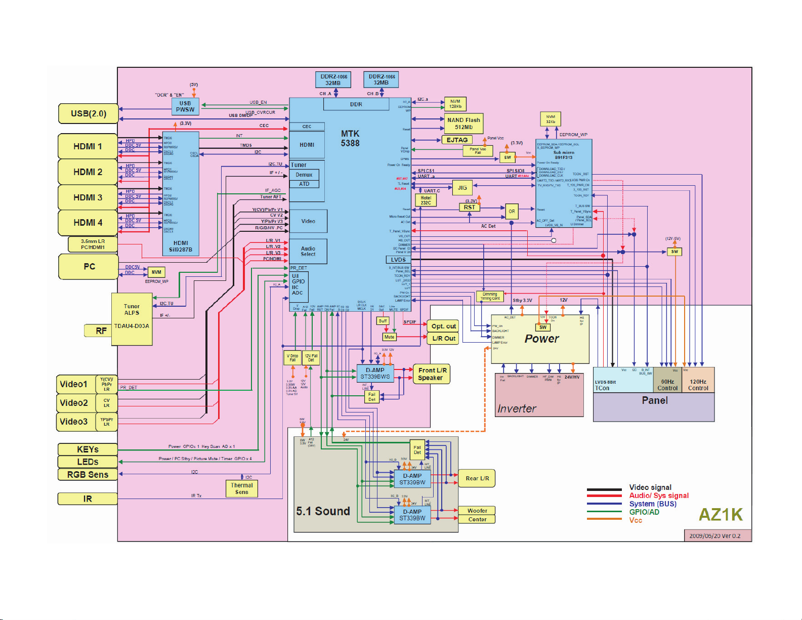
1-3. BLOCK DIAGRAMS
KDL-32FA600
KDL-32FA600
8
Page 9
1-4. SCHEMATICS AND SUPPORTING INFORMATION
A BOARD SCHEMATIC DIAGRAM (1 OF 20)
1 | 2 | 3 | 4 | 5 | 6 | 7 | 8 | 9 |
A
—
B
—
C
—
KDL-32FA600
D
—
E
—
F
—
G
KDL-32FA600
A 1/20
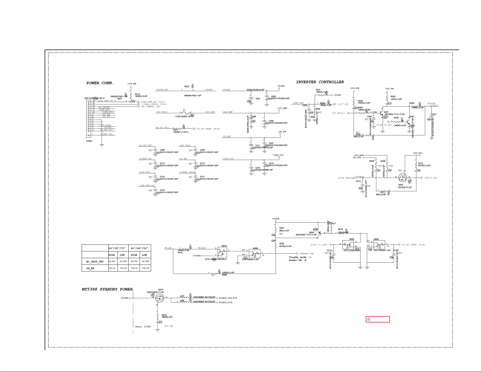
DC CONVERTER I
1-857-593-11 <AZ1K> A-P1
9
Page 10
A BOARD SCHEMATIC DIAGRAM (2 OF 20)
1 | 2 | 3 | 4 | 5 | 6 | 7 | 8 | 9 |
A
—
B
—
C
—
KDL-32FA600
D
—
E
—
F
—
G
KDL-32FA600
A 2/20
DC CONVERTER II
1-857-593-11 <AZ1K> A-P2
10
Page 11
A BOARD SCHEMATIC DIAGRAM (3 OF 20)
1 | 2 | 3 | 4 | 5 | 6 | 7 | 8 | 9 |
A
—
B
—
C
—
KDL-32FA600
D
—
E
—
F
—
G
KDL-32FA600
A 3/2 0
DC CONVERTER III
1-857-593-11 <AZ1K> A-P3
11
Page 12
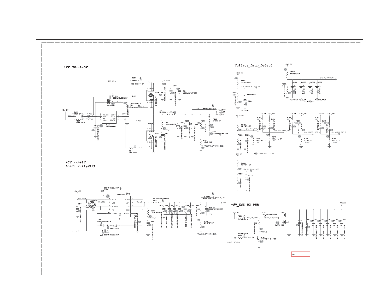
A BOARD SCHEMATIC DIAGRAM (4 OF 20)
1 | 2 | 3 | 4 | 5 | 6 | 7 | 8 | 9 |
A
—
B
—
C
—
KDL-32FA600
D
—
E
—
F
—
G
KDL-32FA600
A 4/2 0
INPUT ANALOG VIDEO
1-857-593-11 <AZ1K> A-P4
12
Page 13

A BOARD SCHEMATIC DIAGRAM (5 OF 20)
1 | 2 | 3 | 4 | 5 | 6 | 7 | 8 | 9 |
A
—
B
—
C
—
KDL-32FA600
D
—
E
—
F
—
G
KDL-32FA600
A 5/20
INPUT D SUB
1-857-593-11 <AZ1K> A-P5
13
Page 14

A BOARD SCHEMATIC DIAGRAM (6 OF 20)
1 | 2 | 3 | 4 | 5 | 6 | 7 | 8 | 9 |
A
—
B
—
C
—
KDL-32FA600
D
—
E
—
F
—
G
KDL-32FA600
A 6/20
INPUT HDMI I
1-857-593-11 <AZ1K> A-P6
14
Page 15

A BOARD SCHEMATIC DIAGRAM (7 OF 20)
1 | 2 | 3 | 4 | 5 | 6 | 7 | 8 | 9 |
A
—
B
—
C
—
KDL-32FA600
D
—
E
—
F
—
G
KDL-32FA600
A 7/20
INPUT HDMI II
1-857-593-11 <AZ1K> A-P7
15
Page 16

A BOARD SCHEMATIC DIAGRAM (8 OF 20)
1 | 2 | 3 | 4 | 5 | 6 | 7 | 8 | 9 |
A
—
B
—
C
—
KDL-32FA600
D
—
E
—
F
—
G
KDL-32FA600
A 8/20
INPUT HDMI SW
1-857-593-11 <AZ1K> A-P8
16
Page 17

A BOARD SCHEMATIC DIAGRAM (9 OF 20)
1 | 2 | 3 | 4 | 5 | 6 | 7 | 8 | 9 |
A
—
B
—
C
—
KDL-32FA600
D
—
E
—
F
—
G
KDL-32FA600
A 9/20
TUNER
1-857-593-11 <AZ1K> A-P9
17
Page 18

A BOARD SCHEMATIC DIAGRAM (10 OF 20)
1 | 2 | 3 | 4 | 5 | 6 | 7 | 8 | 9 |
A
—
B
—
C
—
KDL-32FA600
D
—
E
—
F
—
G
KDL-32FA600
A 10/20
AUDIO IN
1-857-593-11 <AZ1K> A-P10
18
Page 19

A BOARD SCHEMATIC DIAGRAM (11 OF 20)
1 | 2 | 3 | 4 | 5 | 6 | 7 | 8 | 9 |
A
—
B
—
C
—
KDL-32FA600
D
—
E
—
F
—
G
KDL-32FA600
A 11/20
MT5388 INPUT
1-857-593-11 <AZ1K> A-P11
19
Page 20

A BOARD SCHEMATIC DIAGRAM (12 OF 20)
1 | 2 | 3 | 4 | 5 | 6 | 7 | 8 | 9 |
A
—
B
—
C
—
KDL-32FA600
D
—
E
—
F
—
G
KDL-32FA600
A 12/20
MT5388 DDR II
1-857-593-11 <AZ1K> A-P12
20
Page 21

A BOARD SCHEMATIC DIAGRAM (13 OF 20)
1 | 2 | 3 | 4 | 5 | 6 | 7 | 8 | 9 |
A
—
B
—
C
—
KDL-32FA600
D
—
E
—
F
—
G
KDL-32FA600
A 13/20
MT5388 LVDS
1-857-593-11 <AZ1K> A-P13
21
Page 22

A BOARD SCHEMATIC DIAGRAM (14 OF 20)
1 | 2 | 3 | 4 | 5 | 6 | 7 | 8 | 9 |
A
—
B
—
C
—
KDL-32FA600
D
—
E
—
F
—
G
KDL-32FA600
A 14/20
MT5388 PERIPHERAL/FLASH
1-857-593-11 <AZ1K> A-P14
22
Page 23

A BOARD SCHEMATIC DIAGRAM (15 OF 20)
1 | 2 | 3 | 4 | 5 | 6 | 7 | 8 | 9 |
A
—
B
—
C
—
KDL-32FA600
D
—
E
—
F
—
G
KDL-32FA600
A 15/20
MT5388 INPUT
1-857-593-11 <AZ1K> A-P15
23
Page 24

A BOARD SCHEMATIC DIAGRAM (16 OF 20)
1 | 2 | 3 | 4 | 5 | 6 | 7 | 8 | 9 |
A
—
B
—
C
—
KDL-32FA600
D
—
E
—
F
—
G
KDL-32FA600
A 16/20
AUDIO AMP
1-857-593-11 <AZ1K> A-P16
24
Page 25

A BOARD SCHEMATIC DIAGRAM (17 OF 20)
1 | 2 | 3 | 4 | 5 | 6 | 7 | 8 | 9 |
A
—
B
—
C
—
KDL-32FA600
D
—
E
—
F
—
G
KDL-32FA600
A 17/20
AUDIO SPDIF LINEOUT
1-857-593-11 <AZ1K> A-P17
25
Page 26

A BOARD SCHEMATIC DIAGRAM (18 OF 20)
1 | 2 | 3 | 4 | 5 | 6 | 7 | 8 | 9 |
A
—
B
—
C
—
KDL-32FA600
D
—
E
—
F
—
G
KDL-32FA600
A 18/20
IR/USB/KEYPAD
1-857-593-11 <AZ1K> A-P18
26
Page 27

A BOARD SCHEMATIC DIAGRAM (19 OF 20)
1 | 2 | 3 | 4 | 5 | 6 | 7 | 8 | 9 |
A
—
B
—
C
—
KDL-32FA600
D
—
E
—
F
—
G
KDL-32FA600
A 19/20
MCU I
1-857-593-11 <AZ1K> A-P19
27
Page 28

A BOARD SCHEMATIC DIAGRAM (20 OF 20)
1 | 2 | 3 | 4 | 5 | 6 | 7 | 8 | 9 |
A
—
B
—
C
—
KDL-32FA600
D
—
E
—
F
—
G
KDL-32FA600
A 20/20
MCU II
1-857-593-11 <AZ1K> A-P20
28
Page 29

A
[DC CONVERTER I, DC CONVERTER II, DC CONVERTER III, INPUT ANALOG VIDEO, INPUT D SUB, INPUT HDMI I, INPUT HDMI II, INPUT HDMI SW, TUNER, AUDIO IN, MT5388 INPUT, MT5388 DDR II, MT5388
LVDS, MT5388 PERIPHERAL/FLASH, MT5388 INPUT, AUDIO AMP, AUDIO SPDIF LINEOUT, IR/USB/KEYPAD, MCU I, MCU II]
COMPONENT SIDE
1 | 2 | 3 | 4 | 5 | 6 | 7 | 8 | 9 | 10 |
KDL-32FA600
A
—
B
—
C
—
D
—
E
—
F
—
G
—
H
CN6601
R6035
D6453
R6034
CN6451
IC6453IC6454
CN6452
CN902
D6452D6451
C6313C6314
R6461
D810
C829
TP809
CN6003
R6454R6453
R6455
R820
R6460
R6451R6452
R6610
R6611
R6037
R6036
D6456
C827
C830
T
P81
0
D809
R819
C828
C6024
C6025
D901
D902
L902
C6452
C6455
R6456
C6316
D6455
D6602
C232
D6454C6315
C6608
C917
C916
IC302
C304
D6303
R6031
D6302
C6310
R6304
R6457
R6458
TP6601
D6007
R6026
R6028
C6026
RN303
C320
IC301
R6612
R6038
TP6014
R3376
R208
C319
R3338
IC6451
IC6452
R6030
D6301
C6309
R6303
IC6304
TP6602
TP6603
C915
C318
TP302
IC6302
IC6303
IC6601
C234
C233
L231
IC901
C918
CN302
C241
R913
C248
R242
C246
C
2
4
4
C247
C245
R915
R914
R303R302
Q233
Q231
C243
R239
R252
L903
CN6301
R6607
R6606
C6609
R6321
C235
R396
R912
IC6301
CN6302
R6604
IC231
CN901
R6032R6033
D6305D6304
C6311C6312
R6308R6307
R3312
R6605
IC305
L269
D234
C242
R395
R347
X301
TP322
TP324R399
C315 C314R362
TP352
C310
D6307
R3363
R6310
C6303
R6302
R6309
R3351
R6301
TP362
TP
TP358
TP356
TP353
360
R336
R321
R352
R3307
R3309
R339
R351
C231
R251
R317
R316
C344
CN303
C8318
TP363
CN301
L235
C240
R250
R346
R324
R345
R344
R322
R343
R240
CN6001
C345
R3355
Q313
R3366
C238
R243
R385
C239
R3349
C237
C316
C8312
TP321
C317
R241
CN304
R3310
C4317
R6459
Q315
C307
R3347
R3348
R3362
R6311
C335
R6306
C6305
R6305
IC303
TP347
TP345
TP344
TP343
R3325
R335
TP354R3326
R238
R245
R256
Q234
R315
TP326
TP310
R4304
R8318
C8315
R8309
TP368
CN801
R270
R4308
R3320
R4321
TP364
L
306
R8180
TP6003
R244
Q4301
R4360
R4359
R8196
IC4305
C8321
R4309
R4320
R6006
R6003
C8209
R392
R4310
TP305
R8193
R8178
R8181
R4306
R4305
R8194
R388
C8304
R8302
C8303
R8301
R4311
R4319
R4316
TP306
R6185
R8192
R4303
C8210
R4302
C301
C8307
R4324
R4323
C305
D8151
C277
IC267
C312
C313
C8308
R4315
R6186
R4325
R916
R906
R387
R4322
TP8157
Q8154
L283
D8302
D8301
L302
R4165
C276
R4157
T
P
4302
R4158
C311
R325
Q303
R4347
L8157
C281
R4346
C282
CN8153
R6189
R6188
C4314
C283
IC308
C321
R332
R320
C328
C911
C902
R902
CN4303
TP6157
TP6156
TP6155
CN6002
C4315
C4316
IC4304
D4306
C280
C285
C284
R8206
C8189
R3385
IC6152
CN4301
C4313
C4312
R4348
R4312
C908
R907
C8190
R4179
C912
R3384
R911
Q901Q902
R276
R3386
IC268
C914
C289
C288
R3383
R4159
C291
R901
CN8301
C8152
C292
CN6151
TP8155
R8171
R905R910
Q904
R6165
R6163
R6161
R6159
R6156
R6015
R6017
R8304
C8320
C8310
L8156
L901
C910
R909
TP8304
C8175
R8326
C8170
C8176
CN8151
C907
C904
R903
H3
C6164
C6161
C6158
C6157
C6154
C6012
C6013
C6002
R6002
R8162
R4160
R904
C6001
R6001
C6005
R6005
Q903
C6003
R6010
D807
R908
C6006
R6014
C817
C818
D805
TP805
C6011
R6027
R813
R814
L8303
C6031
R8303
TP8154
C6022
C290
L273
C4004
Q400
C4306
C4305
TP270
C4519
C4520
C4475
C4476
L207
C8311
IC8151
TP4043
C822
R4001
IC8301
TP8153
R4332
R4318
R4326
R4314
R6025
C8317C8309
TP807
L8154
TP8302
R8325
C8178
R4317
R512
R8167
R233
TP8152
R508
R4340
R4333
C8174
R4313
C4309
C4308
IC4001
C6015R6021
C6016
C6021
C4307
R510
IC4303
TP369
X4301
R8310
C8327
R8307
R8305
C8326
R8311
R8317R8315
C8329
R8316
R8313
C8328
L8153
R8155
C8165
R504
R506
C816
C4302R4301
R8182
Q8157
R8183
L8155
CN8152
H2
R502
TP4022
RN501
RN507
RN503RN505
IC502
C511
C512
TP4029
R4002
L4003
L4002
L4301
C4304
C4303
R4112
R4113
R801
R802
R810
R812
C801
C802
R8308
R8306
L289
C286
IC271
C8313
C8319
C8302
R4192
R8327
L8151
TP8151
C8151
C206
1-881-683-11
C814
L8301
C8325
L4004
L8152
R8154
D8002
D8001
R8153
R8158
R8151
R8152
L4001
R4111
R809
C813
R811
C815
C201
R8163
R4005
C8204
C260
R817
C825
C279
RN509
R8170R8173
R8164
R4008
R818
C826
R8165
C8186
L4005
C254
Q210
C8214
C250
L236
C8218
RN8151
CN201
Q302
C8217
R6316
C253
C205
C213
C202
R223
C8216
R6318
L4006
R287
R373
R377
D301
R379R378
R232
C223
R212R236
C208
R3324
R8160
C8168
C8169
C8167
R513
R509
C515
R4337
R258
IC232
F1
RN302
C309
R312
C8166
C251
Q209
R308
R307
C252
C249
R214
R288
C308
R8161
C306
R511
R263
TP351
TP342
R342
C324
R3305
C519
SW707
SW704
SW705
R310
C6308
R6313
TM701
C265
R257
R262
C259
C266
C209
R375
R376
R380
R381
R382
R301
C303
R503
R6317
C255
R261
C257
R505
RN502RN506
Q6301
R6315
R6320
R6314
C8323
C258
R4351
C4310
R4344
C211
C207
C212
R6312
L705
C705
R704
R702
R255
R4341
R507
C6307
L706
C704
R705
R703
C535
Q6302
R8321
C273
C272
C4311
R4345
L702
C222
D4304
R952
R950
C210
C216
H4
D904D903
R953R951
C950C951
R281 C264
IC503
R280
H1
C8324
R4203
L234
CN8302
R8322
Q8306
SW703
C713
C709
C701
C710
C711
L707
C274
R3343
R3364
IC310
Q207
R226
C215
CN950
C298
C4157
R4202
L4157
L4158
R4155
R4208
L410
L411
L412
L413
L414
L415
L418
L419
L416
L417
L422
L423
L400
L401
L402
L403
L404
L405
L408
L409
L406
L407
L420
L421
R4195
C333
R4183
IC266
R3341R3345
R4166
C702
C336
C4155
CN4152
C4156
R4161
R4201
R4209
CN4151
SW706
SW701
SW702
C271
C270
R267
R285
R3365
C343
R3353
R3342
Q314
C340
R3356
D302
C341
R204
R201
R3354
R3350
R206
C337
C203
IC311
C330
IC309
C217
C218
R231
R3371
R3346
L292
R4178
R4177
KDL-32FA600
29
Page 30

A
[DC CONVERTER I, DC CONVERTER II, DC CONVERTER III, INPUT ANALOG VIDEO, INPUT D SUB, INPUT HDMI I, INPUT HDMI II, INPUT HDMI SW, TUNER, AUDIO IN, MT5388 INPUT, MT5388 DDR II, MT5388
LVDS, MT5388 PERIPHERAL/FLASH, MT5388 INPUT, AUDIO AMP, AUDIO SPDIF LINEOUT, IR/USB/KEYPAD, MCU I, MCU II]
CONDUCTOR SIDE
1 | 2 | 3 | 4 | 5 | 6 | 7 | 8 | 9 | 10 |
C909
C903
C901
C906
C913
A
—
B
—
C
—
D
—
E
—
C6456
C6454
C6453
C6451
D6001
C6602
C6163
C6605
C6306
C6601
D6004
TP6001
TP355
C6302
R
6
61
C6607
3
TP6008
R6029
L6001
C6304
C6606
R6004
R6008
C6604
C6603
R6609
R6608
L6004
C6301
D6306
R6007
R6016
R6319
C6004
R6018
C6014
R6019
C905
TP367
TP366
TP365
D6005
TP6010
D6002
TP6004
R3308
R3303
TP350
R4197 R334
R4190 R333
R3352
R3379
R3380
TP328
C806
C803
R3377
R
3
2
3
Q316
C804
D802
L6005
R6020
TP323
Q312
R3357
R6022
R313
TP318
R804
C6017
R4189
C325
R314
R3302
TP340
TP337
TP339
TP357
TP359
TP801
R6009
L6002
TP314
R4210
R4211
R3378
TP348
TP361
C6019
C6007
R6011
R394
TP333
R3327
TP320
TP346
D6006
C302
TP334
TP330
TP349
R3369
C805
TP336
R337
R338
R350
Q8305Q8301
TP802
R803
TP317
Q311
TP6012
L6006
C6020
TP335TP312
TP325
TP307
R6024
R6023
TP311
R4194
R4200
Q8302
C8322
C8316
D6156D6157
D801
C6018
TP319
R4336
R8323
C6153
D6153
R4328
R4327
R4334
R6153
R6152
TP6151
C6156
R6157
L6154
Q8303
C
6
R6151
1
R6154
52
D6151D6152
D6154
L6155
Q6153
R4350
R6180
R6184
TP6152
C6160
C6170
R6187
R6181
R6162
TP806
D6601
R6183
R6179
R6171
D6155
R6158
D806
C300
C4516
L712
C533
R712
C297
C299
C534
C296
C919
R290
RN508
R291
IC269
C295
C526
C505
C527
C528
C532
C513
C529
C530
C518
C4487
R713
R264
C322
R260
R284
R282
R283
R266
R8314
C293
TP269
R4191
C323
R4162
R4186
R277
C294
L293
D4301
R4168 R4167
R4199
R4184
R4188
R4339
R4164
R4187
R4196
R4354
R4363
R4193
R4182
R4185
C446
R3373
R4198
C504
C4497
C4472
C4471
C4501
C4521
C4522
C509
C4496
C4488
C4504
C4503
L276
R501
C4455
C4457
C4456
C4452
C4463
L209
L210
C541C531
C501
C287
C4458
C4451
C4454
C4466
TP4024
D4310
C522
C523
C4486
C536
C4453
D4309
C4485
C520
C4465
C4508
R274
D4308
C548
C549
C537
C545
R275
C524
TP502
C547
TP4020
C8206
C8219
R706
R701
C263
R279
C525
C4517
C4518
C514
TP5
01
R4330
C8196C8194
R278
R268
C718
C712
C4462
R254
R265
R4342
R4353
R709
C4459
C4468
R4451
L287
L286
RN504
RN510
C506
C540
R708
C4484
R259
R4343
R4352
C715
L272
R4329
L709
C720
L719
L711
C708
C4483
C4506
C4507
R4331
C4505
C716
R707
L284
R4335
R4003
C4495
C4498
C4499
C721
C719
C516
R8319
L708
C508
C510
C538
C539
C4003
L285
Q8304
R8195
C707
C714
L713
C717
L710
L704
C542
C4509
C4510
C517
TP4301
C544
C543
C546
C521
IC4302
R6182
C4470
L278
Q6152
C823
C824
R6176
R6168
C6162
C6151
TP6153
R816
D808
D6158
D6159
C6166
C819
R6166
L6156
C6169
C6168
R815
Q6151
R6173
R6175
C820
R6170
R4349
TP808
R6178R6177
Q213
R4007
R4181
R4156
R4163
TP6154
R4006
R218
R4338
L274
TP4042
C4469
C4473
L291
C4494
C4493
C4491
C4492
C4515
C4479
C4480
L208
C4514
L2
7
1
C4482
C4481
L288
L290
C
44
77
C4460
C4464
C4512
C4478
C4474
L270
C4500
C4461
C4513
C4511
C4502
C4001
C507
C4467
C4002
C4490
C4489
L275
L277
R3337
Q304
Q305
KDL-32FA600
R3336
C445
F
—
G
—
H
KDL-32FA600
R246
TP329
TP6006
C6009
C6008
R235
R234
D232
R8198
C8200
C8202
C8205
C8207
TP338
TP332
TP341
TP331
TP370
R6013
C6010
R6012
L6003
R4361
C821
D6003
C278
R273
R8199
R272
IC8153
C8197
C8215
C8203
C8198
C8195
C8213
C8199
R8210
R8209
C8201
R4355
R4356
IC4301
R4358
R4357
R4362
C4301
R8211
R8212
R8213
IC8152
R8202
C8193
R8203
R8204
R8330
R8331
R8207
C8156
C8155
C8157
C8154
Q8156
R8166
TP8158
C8184
R8189
R8184
TP8159
Q8158
C8185
R8157
C8162
C8163
C8164
R8201
R8188Q8160
C8187
R8197
TP8160
R8187
R8200
C8153
C8160
C8159
C8158 C8161
1-881-683-11
R8156
R8176
Q8155
R8186
Q8153
C8192
R8205
R8208
C8188
C8212
C8211
C8191
C8183
R8179
TP8156
R8185
R8175
R8174
C8180
C8171
C8179
C8172
C8181
C8173
C8177 C8182
C220
Q206
C219
Q205
R269
R217
R219
Q204
R227
L279
R3375
R3358
R3359
R222
C221
R203
R207
R202
C334
R3360
C204
R3370
C339C338
Q201
C332
R3372
L307
C329
C342
R3361
R3367
R205
R3340
Q202
R3344
C214
R210
R209
C706
L703
R711
R3368
R211
30
Page 31

G2HE BOARD SCHEMATIC DIAGRAM
1 | 2 | 3 | 4 | 5 | 6 | 7 | 8 | 9 | 10 | 11 | 12 | 13 | 14 | 15 | 16 | 17 | 18 | 19 | 20 | 21 |
A
—
B
—
C
—
KDL-32FA600
D
—
E
—
F
—
G
—
H
—
I
—
J
—
K
—
L
—
M
—
'(%
N
0/7%2
—
O
—
P
KDL-32FA600 31
!:+'(%0
Page 32

KDL-32FA600
G2HE
1 | 2 | 3 | 4 | 5 | 6 | 7 | 8 | 9 | 10 | 11 | 12 |
A
—
B
—
C
—
[POWER]
COMPONENT SIDE
D
—
E
—
KDL-32FA600
32
Page 33

KDL-32FA600
G2HE
1 | 2 | 3 | 4 | 5 | 6 | 7 | 8 | 9 | 10 | 11 | 12 |
A
—
B
—
C
—
[POWER]
CONDUCTOR SIDE
D
—
E
—
KDL-32FA600
33
Page 34

H2 BOARD SCHEMATIC DIAGRAM
1 | 2 | 3 | 4 | 5 | 6 | 7 | 8 | 9 | 10
A
—
B
—
C
H2
A
[IR/LED]
COMPONENT SIDE
1 | 2 | 3 |
S32M88 IR Board
U9104
15
S9206-1
48.71S08.011
U9103 D9102
MADE IN TAIWAN
D9103
KDL-32FA600
D9104
—
D
—
E
—
F
—
G
—
H2
IR/LED
1-857-594-11 <AZ1K> H2-P1
H2
[IR/LED]
CONDUCTOR SIDE
1 | 2 | 3 |
4119C
51
R9106
R9105
S32M88 IR Board
6219R
19C31
7019R
S9206-1
8019C
7
0
48.71S08.011
19C
19C05
MADE IN TAIWAN
19C
3
P
L9101
T
213
15
9
0
R91 72
C9122
319R2
2
1
19C91
9R1 C33
9C
9C121
TP1
TP2
9C116
L9 201
D9112 D9113
C9106
D9107
D9108
2119R
1
11
9R
TP7
C9110
C9109
71
TP6
3
1
0
TP5
9C
1
9
1
9
TP4
L
1
0
1
19
9D
C9103
D
2019C
1019C
CN9101
6019D
0119D
C9111
R9110
C9112
R9109
KDL-32FA600
34
Page 35

KD BOARD SCHEMATIC DIAGRAM (1 OF 2)
1 | 2 | 3 | 4 | 5 | 6 | 7 | 8 | 9 | 10 | 11 | 12 |
KDL-32FA600
A
—
B
—
C
—
D
—
E
—
F
—
G
—
H
—
+24V
12
C843
C843
Close CN807
SCD1U50V3KX-GP
SCD1U50V3KX-GP
+3.3V_A
+3.3V_A
LO= Mute
Mute Function
+3.3V_A
100KR2J-1-GP
100KR2J-1-GP
R826
R826
A_SPK_C-
2
100KR2J-1-GP
100KR2J-1-GP
R836
R836
A_SPK_C+
R839
A_SPK_W-
A_SPK_W+
R839
100KR2J-1-GP
100KR2J-1-GP
R846
R846
100KR2J-1-GP
100KR2J-1-GP
AMP_VDD
F801
12
C840
C840
E100U35VM-3-GP
E100U35VM-3-GP
A_VDD_REG
A_VCC_REG
A_VDD_PLL
A_AOMCLK
A_AOBCK
A_AOLRCK
A_SDI
A_SDI
A_SDA_AMP
A_SCL_AMP
A_REST_AMP
A_AMP_INT
12
C891
C891
SCD1U50V3KX-GP
SCD1U50V3KX-GP
A_SPK_C-_2
A_SPK_C+_2
A_SPK_W-_2
Q807
Q807
F801
1 2
FUSE-6D3A24V-GP
FUSE-6D3A24V-GP
E100U35VM-3-GP
E100U35VM-3-GP
15
21
36
11
8
5
24
27
28
29
2
30
33
34
31
3
23
16
32
Q802
Q802
B
2SA1235A-T112-1F-GP
2SA1235A-T112-1F-GP
E
C
C
E
Q804
Q804
2SA1235A-T112-1F-GP
2SA1235A-T112-1F-GP
B
B
C
E
C
E
Q808
Q808
2SA1235A-T112-1F-GP
2SA1235A-T112-1F-GP
B
IC802
IC802
VDD
VDD_DIG
VDD_DIG
VCC
VCC
VCC_REG
VDD_PLL
XTI
BICKI
LRCKI
SA
SDI
SDA
SCL
RESET
TEST_MODE
PWRDN
CONFIG
INT_LINE
STA339BW13TR-GP
STA339BW13TR-GP
A_SPK_WC+-
C837
C837
12
L802
L802
1 2
HCB3216KF-121T40-GP
HCB3216KF-121T40-GP
L809
L809
1 2
HCB3216KF-121T40-GP
HCB3216KF-121T40-GP
C825 SC1U25V5KX-1GPC825 SC1U25V5KX-1GP
C826 SC1U25V5KX-1GPC826 SC1U25V5KX-1GP
C817 SCD1U50V3KX-GPC817 SCD1U50V3KX-GP
L805 FCM1608K-151T06-GPL805 FCM1608K-151T06-GP
12
C884
C884
SDA_AMP
SCL_AMP
GPIO7
MUTE_N A_MUTE_N
AMP_ERR_3 A_VDD_REG_1
R820
R820
1 2
10KR3J-L1-GP
10KR3J-L1-GP
R823
R823
47KR3J-L-GP
47KR3J-L-GP
NC
NC
A_SPK_C-_1
1
C834
C834
SC1U25V3KX-1-GP
SC1U25V3KX-1-GP
A_SPK_C+_1
12
A_SPK_W-_1
12
C838
C838
SC22U6D3V5MX-2GP
SC22U6D3V5MX-2GP
A_SPK_W+_1
12
12
12
C802
C802
C883
C883
SCD1U50V3KX-GP
SCD1U50V3KX-GP
1
2
2
1
R829 0R0603-PAD-1-GPR829 0R0603-PAD-1-GP
1 2
R831 0R0603-PAD-1-GPR831 0R0603-PAD-1-GP
1
AMP_VDD_IC802
2
1
1 2
100KR2J-1-GP
100KR2J-1-GP
1 2
NC
NC
R8180
R8180
AOMCLK
AOBCK
AOLRCK
AOSDATA1
RN801
RN801
SRN100J-5-GP
1
1 2
1 2
1 2
1 2
R830
R830
12
100KR3J-L-GP
100KR3J-L-GP
R843
R843
12
100KR3J-L-GP
100KR3J-L-GP
SRN100J-5-GP
2
0R0402-PAD-1-GP
0R0402-PAD-1-GP
R814 100R3J-4-GPR814 100R3J-4-GP
SCD1U50V3KX-GP
SCD1U50V3KX-GP
R815 100R3J-4-GPR815 100R3J-4-GP
R816 100R3J-4-GPR816 100R3J-4-GP
R818 0R0402-PAD-1-GPR818 0R0402-PAD-1-GP
R819 10KR3J-L1-GPR819 10KR3J-L1-GP
+3.3V_A
12
12
12
12
12
C803
C803
R8181
R8181
1MR5J-1-GP
1MR5J-1-GP
E4700U35VM-GP
E4700U35VM-GP
E4700U35VM-GP
E4700U35VM-GP
2
As close as possible to the pin
1
2
3
4 5
R821
R821
1 2
10KR3J-L1-GP
10KR3J-L1-GP
1
0R0402-PAD-1-GP
0R0402-PAD-1-GP
1 2
0R0402-PAD-1-GP
0R0402-PAD-1-GP
1
0R0402-PAD-1-GP
0R0402-PAD-1-GP
1
47KR3J-L-GP
47KR3J-L-GP
R827
R827
R837
R837
R840
R840
R847
R847
NC
NC
R824
R824
8
7
6
2
2
2SA1235A-T112-1F-GP
2SA1235A-T112-1F-GP
2
12
C839
C839
A_VDD_DIG1
A_VDD_DIG2
12
A_SPK_W+_2
12
C805
C805
SC1U50V6KX-GP
SC1U50V6KX-GP
OUT3A/FFX3A
OUT3B/FFX3B
EAPD/OUT4B
TWARN/ OUT4A
FILTER_PLL
MUTE_N[3]
GPIO7[3]
SDA_AMP[3]
SCL_AMP[3]
1KR3J-L1-GP
1KR3J-L1-GP
R835
R835
SC1U25V3KX-1-GP
SC1U25V3KX-1-GP
AMP_VDD_IC802
C806
C806
12
SCD1U50V3KX-GP
SCD1U50V3KX-GP
OUT1A
OUT1B
OUT2A
OUT2B
GND_PLL
VSS
GND
GND
GND
GND_DIG
GND_DIG
GND_SUB
GND_REG
A_SPK_WC+-_1
12
12
12
C877
C877
C878
C878
SC1U50V6KX-GP
SC1U50V6KX-GP
SCD1U50V3KX-GP
SCD1U50V3KX-GP
A_OUT2_W+
13
A_OUT2_W-
10
A_OUT1_C+
9
A_OUT1_C-
6
18
17
19
20
A_PLL2
R811
R811
25
2
2K2R3J-1-GP
2K2R3J-1-GP
26
A_VSS
4
C821 SCD1U50V3KX-GPC821 SCD1U50V3KX-GP
7
12
37
22
35
1
14
MOVE BYPASS C TO Pin 21 & Pin 36
+3.3V_A+3.3V_A
12
R842
R842
4K7R3J-2-GP
4K7R3J-2-GP
AMP_VDD_DROP_DET
MUTE_N
GPIO7
SDA_AMP
SCL_AMP
R871 0R0402-PAD-1-GPR871 0R0402-PAD-1-GP
1 2
R875 0R0402-PAD-1-GPR875 0R0402-PAD-1-GP
1 2
+3.3V_A
12
R838
R838
4K7R3J-2-GP
4K7R3J-2-GP
C
B
12
E
Q805
Q805
R841
R841
2SC3052-T112-1F-GP
2SC3052-T112-1F-GP
10KR3J-L1-GP
10KR3J-L1-GP
C818 SC680P50V3JN-GPC818 SC680P50V3JN-GP
1
2
C819 SC4700P50V2KX-1GPC819 SC4700P50V2KX-1GP
1
A_PLL
1 2
C829 SCD1U50V3KX-GPC829 SCD1U50V3KX-GP
12
R828
R828
4K7R3J-2-GP
4K7R3J-2-GP
12
C836
C836
SC1U25V3KX-1-GP
SC1U25V3KX-1-GP
12
C820 SC100P50V2JN-3GPC820 SC100P50V2JN-3GP
12
2
1
SDA_1
SCL_1
12
12
C890
C890
C895
C895
NC
NC
NC
NC
SC100P50V3JN-2GP
SC100P50V3JN-2GP
AMP_ERR_3
A_VCC_REG
A_VDD_REG
CN805
CN805
1
2
4
3
5
6
7
8
9
10
11
12
13
14
JWT-CONN14D-S8-GP
JWT-CONN14D-S8-GP
Close CN805
D808
D808
SCD1U50V3KX-GP
SCD1U50V3KX-GP
AK
1PS79SB31-1-GP-U
1PS79SB31-1-GP-U
D809
D809
A
K
1PS79SB31-1-GP-U
1PS79SB31-1-GP-U
R845 0R0402-PAD-1-GPR845 0R0402-PAD-1-GP
MCK
1 2
BCK
R848 0R0402-PAD-1-GPR848 0R0402-PAD-1-GP
1
LRCK
R849 0R0402-PAD-1-GPR849 0R0402-PAD-1-GP
1 2
DA1
R850 0R0402-PAD-1-GPR850 0R0402-PAD-1-GP
1 2
DA2
R851 0R0402-PAD-1-GPR851 0R0402-PAD-1-GP
1
12
12
C845
C845
C902
C902
SCD1U50V3KX-GP
SCD1U50V3KX-GP
SC4D7U10V3KX-GP
SC4D7U10V3KX-GP
AMP_ERR_2 [3]
3
1 2
A_OUT1_C-
12
C835
C835
NC
NC
SC220P50V2JN-3GP
SC220P50V2JN-3GP
A_OUT1_C+
12
C870
C870
NC
NC
SC220P50V2JN-3GP
SC220P50V2JN-3GP
12
12
2
2
+3.3V_1
12
C896
C896
NC
NC
SC100P50V3JN-2GP
SC100P50V3JN-2GP
+3.3V_A +3.3V_A
D801
D801
BAV99-8-GP
BAV99-8-GP
NC
NC
L803 IND-22UH-122-GPL803 IND-22UH-122-GP
12
22R3J-2-GP
22R3J-2-GP
L806 IND-22UH-122-GPL806 IND-22UH-122-GP
A_OUT2_W-
C871
C871
NC
NC
SC220P50V2JN-3GP
SC220P50V2JN-3GP
A_OUT2_W+
C874
C874
NC
NC
SC220P50V2JN-3GP
SC220P50V2JN-3GP
C897
C897
12
NC
NC
SDA_AMPSCL_AMP
1
R806
R806
A_OUT1_C
SCD1U50V3KX-GP
SCD1U50V3KX-GP
12
C816
C816
SC330P50V2KX-3GP
SC330P50V2KX-3GP
1 2
IND-22UH-105-GP
IND-22UH-105-GP
1 2
12
C827
C827
SC330P50V2KX-3GP
SC330P50V2KX-3GP
A_OUT2_W
12
SCD1U50V3KX-GP
SCD1U50V3KX-GP
R822
R822
22R3J-2-GP
22R3J-2-GP
1 2
L808
L808
IND-22UH-105-GP
IND-22UH-105-GP
C898
C898
C900
C900
12
12
NC
NC
NC
NC
SC10P50V2JN-4GP
SC10P50V2JN-4GP
SC10P50V2JN-4GP
SC10P50V2JN-4GP
3
1 2
L807
L807
D802
D802
BAV99-8-GP
BAV99-8-GP
NC
NC
CENTER
2
A_OUT_AC-
1 2
C810
C810
SCD1U50V3KX-GP
SCD1U50V3KX-GP
C814
C814
A_OUT_BC+
1 2
SUB WOFFER
A_OUT2_AW-
1
2
C823
C823
SCD1U50V3KX-GP
SCD1U50V3KX-GP
NC
NC
SC10P50V2JN-4GP
SC10P50V2JN-4GP
1 2
C901
C901
12
A_OUT2_BW+
AOMCLK [3]
AOBCK [3]
AOLRCK [3]
AOSDATA2 [3]
AMP_ERR_2 [3]
12
C886
C886
SC10P50V2JN-4GP
SC10P50V2JN-4GP
C832
C832
AOMCLK
AOBCK
AOLRCK
AOSDATA1
C899
C899
12
NC
NC
SC10P50V2JN-4GP
SC10P50V2JN-4GP
SCD1U50V3KX-GP
SCD1U50V3KX-GP
C804
C804
1 2
6D2R5F-GP
6D2R5F-GP
R807
R807
1 2
12
SCD1U50V3KX-GP
SCD1U50V3KX-GP
C813
C813
1 2
6D2R5F-GP
6D2R5F-GP
R808
R808
2
1
SCD1U50V3KX-GP
SCD1U50V3KX-GP
C822
C822
1
2
6D2R5F-GP
6D2R5F-GP
R817
R817
2
1
SCD1U50V3KX-GP
SCD1U50V3KX-GP
C831
C831
2
1
6D2R5F-GP
6D2R5F-GP
R825
R825
1
2
L815 HCB3216KF-601T20-GPL815 HCB3216KF-601T20-GP
1 2
12
C887
C887
SCD1U50V3KX-GP
SCD1U50V3KX-GP
12
C903
C903
SC4D7U10V3KX-GP
SC4D7U10V3KX-GP
KD 1/2
AUDIO AMP
SCD1U50V3KX-GP
SCD1U50V3KX-GP
C811
C811
+3.3V_A
12
C904
C904
C809
C809
1 2
A_SPK_C-
C812
C812
1 2
SC1KP50V2KX-1GP
SC1KP50V2KX-1GP
C815
C815
1 2
SC1KP50V2KX-1GP
SC1KP50V2KX-1GP
SCD47U50V5KX-1GP
SCD47U50V5KX-1GP
SC1KP50V2KX-1GP
SC1KP50V2KX-1GP
12
C830
C830
SCD47U50V5KX-1GP
SCD47U50V5KX-1GP
12
C905
C905
SC4D7U10V3KX-GP
SC4D7U10V3KX-GP
SC4D7U10V3KX-GP
SC4D7U10V3KX-GP
C824
C824
1 2
C833
C833
1 2
AMP_VDD
SC1KP50V2KX-1GP
SC1KP50V2KX-1GP
SC1KP50V2KX-1GP
SC1KP50V2KX-1GP
12
12
A_SPK_C+
C828
C828
1 2
SC1KP50V2KX-1GP
SC1KP50V2KX-1GP
JWT-CON4-6-GP
JWT-CON4-6-GP
R813
R813
100KR2J-1-GP
100KR2J-1-GP
R832
R832
10KR2F-2-GP
10KR2F-2-GP
NC
NC
A_SPK_W-
A_SPK_W+
CN807
CN807
1
2
3
4
3
2
1
CN802
CN802
JWT-CON3-4-GP
JWT-CON3-4-GP
Show TEXT On PCB
L+
L-
Show TEXT On PCB
W+ for Pin 1
W- for Pin 2
CN803
CN803
2
1
SKT-JACK-349-GP
SKT-JACK-349-GP
12
C844
C844
SCD1U50V3KX-GP
SCD1U50V3KX-GP
AMP_VDD_DROP_DET
12
C842
C842
SCD1U50V3KX-GP
SCD1U50V3KX-GP
+24V
I
—
KDL-32FA600
1-857-617-11 <AZ1K> KD-P1
35
Page 36

KD BOARD SCHEMATIC DIAGRAM (2 OF 2)
1 | 2 | 3 | 4 | 5 | 6 | 7 | 8 | 9 | 10 | 11 | 12 | 13
KDL-32FA600
A
—
B
—
C
—
D
—
E
—
F
—
G
—
H
—
C860 SC1U25V5KX-1GPC860 SC1U25V5KX-1GP
1 2
C863 SC1U25V5KX-1GPC863 SC1U25V5KX-1GP
1 2
+3.3V_A
C853 SCD1U50V3KX-GPC853 SCD1U50V3KX-GP
1
L812 FCM1608K-151T06-GPL812 FCM1608K-151T06-GP
GPIO7[2]
MUTE_N[2]
R866
R866
47KR3J-L-GP
47KR3J-L-GP
12
B_SPK_LS+_1
1
B_SPK_RS-_1
12
B_SPK_RS+_1
12
1 2
AOLRCK[2]
AOSDATA2[2]
2
R870
R870
NC
NC
B_SPK_LS-_1
C872
C872
C876
C876
+3.3V_A
+3.3V_A
SDA_AMP[2]
SCL_AMP[2]
12
C885
C885
SCD1U50V3KX-GP
SCD1U50V3KX-GP
LO= Mute
AMP_ERR_4
Mute Function
+3.3V_A +3.3V_A
B_SPK_LS-
B_SPK_LS+
B_SPK_RS-
B_SPK_RS+
1
10KR3J-L1-GP
10KR3J-L1-GP
100KR2J-1-GP
100KR2J-1-GP
R873
R873
100KR2J-1-GP
100KR2J-1-GP
R880
R880
2
100KR2J-1-GP
100KR2J-1-GP
R887
R887
100KR2J-1-GP
100KR2J-1-GP
R898
R898
AMP_VDD
2
AOMCLK[2]
AOBCK[2]
R859
R859
R860
R860
R861
R861
R862 100R3J-4-GPR862 100R3J-4-GP
R863 0R0402-PAD-1-GPR863 0R0402-PAD-1-GP
R865 10KR3J-L1-GPR865 10KR3J-L1-GP
12
12
SC1U25V3KX-1-GP
SC1U25V3KX-1-GP
12
SC1U25V3KX-1-GP
SC1U25V3KX-1-GP
F802
F802
FUSE-6D3A24V-GP
FUSE-6D3A24V-GP
R833 0R0603-PAD-1-GPR833 0R0603-PAD-1-GP
1 2
R834 0R0603-PAD-1-GPR834 0R0603-PAD-1-GP
1 2
AMP_VDD_IC804
100KR2J-1-GP
100KR2J-1-GP
1
NC
NC
R8179
R8179
RN802
RN802
2
1
10KR3J-L1-GP
10KR3J-L1-GP
1 2
100R3J-4-GP
100R3J-4-GP
1
2
100R3J-4-GP
100R3J-4-GP
1 2
1 2
1 2
R867
R867
1 2
10KR3J-L1-GP
10KR3J-L1-GP
47KR3J-L-GP
47KR3J-L-GP
0R0402-PAD-1-GP
0R0402-PAD-1-GP
1 2
12
R876
R876
100KR3J-L-GP
100KR3J-L-GP
0R0402-PAD-1-GP
0R0402-PAD-1-GP
1
0R0402-PAD-1-GP
0R0402-PAD-1-GP
1 2
12
R891
R891
100KR3J-L-GP
100KR3J-L-GP
0R0402-PAD-1-GP
0R0402-PAD-1-GP
1 2
1 2
1
2
3
4 5
B_VDD_REG
B_VDD_DIG1
B_VDD_DIG2
B_VCC_REG
B_VDD_PLL
As close as possible to the pin
2
SRN100J-5-GP
SRN100J-5-GP
R874
R874
R881
R881
R884
R884
R899
R899
R868
R868
NC
NC
2
8
7
6
12
B_AOMCLK
B_AOBCK
B_AOLRCK
B_SDI
B_SA
B_SDA_AMP
B_SCL_AMP
B_REST_AMP
B_MUTE_N
B_AMP_INT
B_SPK_LS-_2
B_SPK_LS+_2
B_SPK_RS-_2
B_SPK_RS+_2
AMP_VDD_IC804
12
C808
C808
C807
C807
SC1U50V6KX-GP
SC1U50V6KX-GP
SCD1U50V3KX-GP
SCD1U50V3KX-GP
15
21
36
11
8
5
24
27
28
29
2
B_SDI
30
33
34
31
3
23
16
32
12
C892
C892
SCD1U50V3KX-GP
SCD1U50V3KX-GP
Q809
Q809
2SA1235A-T112-1F-GP
2SA1235A-T112-1F-GP
B
E
E
Q810
Q810
2SA1235A-T112-1F-GP
2SA1235A-T112-1F-GP
B
B
Q812
Q812
2SA1235A-T112-1F-GP
2SA1235A-T112-1F-GP
E
E
Q815
Q815
2SA1235A-T112-1F-GP
2SA1235A-T112-1F-GP
B
12
12
C889
C889
C888
C888
SC1U50V6KX-GP
SC1U50V6KX-GP
IC804
IC804
VDD
VDD_DIG
VDD_DIG
VCC
VCC
VCC_REG
VDD_PLL
XTI
BICKI
LRCKI
SA
SDI
SDA
SCL
RESET
TEST_MODE
PWRDN
CONFIG
INT_LINE
STA339BW13TR-GP
STA339BW13TR-GP
C
C
B_SPK_LR
C875
C875
C
C
12
12
SCD1U50V3KX-GP
SCD1U50V3KX-GP
OUT3A/FFX3A
OUT3B/FFX3B
EAPD/OUT4B
TWARN/ OUT4A
FILTER_PLL
GND_PLL
GND_DIG
GND_DIG
GND_SUB
GND_REG
1KR3J-L1-GP
1KR3J-L1-GP
R882
R882
SC1U25V3KX-1-GP
SC1U25V3KX-1-GP
OUT1A
OUT1B
OUT2A
OUT2B
VSS
GND
GND
GND
B_SPK_LR_1
12
R888
R888
B_OUTRS+
13
B_OUTRS-
10
B_OUTLS+
9
B_OUTLS-
6
18
17
19
20
B_PLL2
R857
R857
25
2K2R3J-1-GP
2K2R3J-1-GP
26
4
7
12
37
22
35
1
14
C857 SCD1U50V3KX-GPC857 SCD1U50V3KX-GP
B_VSS B_VCC_REG
MOVE BYPASS C TO Pin 21 & Pin 36
B_VDD_REG_1
C855 SC680P50V3JN-GPC855 SC680P50V3JN-GP
C854 SC4700P50V2KX-1GPC854 SC4700P50V2KX-1GP
12
1 2
2
C856 SC100P50V2JN-3GPC856 SC100P50V2JN-3GP
B_PLL
C865 SCD1U50V3KX-GPC865 SCD1U50V3KX-GP
1 2
+3.3V_A
12
R844
R844
4K7R3J-2-GP
4K7R3J-2-GP
12
C
C873
B
12
10KR3J-L1-GP
10KR3J-L1-GP
C873
SC1U25V3KX-1-GP
SC1U25V3KX-1-GP
E
Q811
Q811
2SC3052-T112-1F-GP
2SC3052-T112-1F-GP
12
1
12
B_VDD_REG
AMP_ERR_4
D810
D810
A
K
1PS79SB31-1-GP-U
1PS79SB31-1-GP-U
D811
D811
AK
1PS79SB31-1-GP-U
1PS79SB31-1-GP-U
B_OUTLS-
12
C879
C879
NC
NC
SC220P50V2JN-3GP
SC220P50V2JN-3GP
B_OUTLS+
12
C880
C880
NC
NC
SC220P50V2JN-3GP
SC220P50V2JN-3GP
B_OUTRS-
12
C881
C881
NC
NC
SC220P50V2JN-3GP
SC220P50V2JN-3GP
B_OUTRS+
12
C882
C882
NC
NC
SC220P50V2JN-3GP
SC220P50V2JN-3GP
AMP_ERR_2 [3]
L810 IND-22UH-122-GPL810 IND-22UH-122-GP
1 2
12
R852
R852
22R3J-2-GP
22R3J-2-GP
B_OUT1
12
C852
C852
SC330P50V2KX-3GP
SC330P50V2KX-3GP
L813 IND-22UH-122-GPL813 IND-22UH-122-GP
1
L801 IND-22UH-122-GPL801 IND-22UH-122-GP
1
12
C862
C862
SC330P50V2KX-3GP
SC330P50V2KX-3GP
B_OUT2
12
R869
R869
22R3J-2-GP
22R3J-2-GP
L814 IND-22UH-122-GPL814 IND-22UH-122-GP
1
REAR L
1 2
C846
C846
SCD1U50V3KX-GP
SCD1U50V3KX-GP
SCD1U50V3KX-GP
SCD1U50V3KX-GP
C851
C851
1 2
2
REAR R
2
1 2
C861
C861
SCD1U50V3KX-GP
SCD1U50V3KX-GP
SCD1U50V3KX-GP
SCD1U50V3KX-GP
C868
C868
1 2
2
B_OUTLS_B-
B_OUTLS_B+
SCD1U50V3KX-GP
SCD1U50V3KX-GP
B_OUTRS_A-
SCD1U50V3KX-GP
SCD1U50V3KX-GP
B_OUTRS_A+
SCD1U50V3KX-GP
SCD1U50V3KX-GP
C841
C841
1 2
6D2R5F-GP
6D2R5F-GP
R853
R853
1 2
SCD1U50V3KX-GP
SCD1U50V3KX-GP
C849
C849
1 2
6D2R5F-GP
6D2R5F-GP
R854
R854
1
C858
C858
1 2
6D2R5F-GP
6D2R5F-GP
R864
R864
1
C867
C867
1 2
6D2R5F-GP
6D2R5F-GP
R872
R872
1
12
C847
C847
2
2
2
SCD47U50V5KX-1GP
SCD47U50V5KX-1GP
12
C866
C866
SCD47U50V5KX-1GP
SCD47U50V5KX-1GP
KD 2/2
AUDIO AMP
B_SPK_LS-
C801
C801
1 2
SC1KP50V2KX-1GP
SC1KP50V2KX-1GP
C850
C850
1 2
SC1KP50V2KX-1GP
SC1KP50V2KX-1GP
B_SPK_LS+
B_SPK_RS-
C859
C859
1 2
SC1KP50V2KX-1GP
SC1KP50V2KX-1GP
C869
C869
1 2
SC1KP50V2KX-1GP
SC1KP50V2KX-1GP
B_SPK_RS+
C848
C848
1 2
SC1KP50V2KX-1GP
SC1KP50V2KX-1GP
Show TEXT On PCB
[Ls+] for Pin 3
[Ls-] for Pin 4
CN801
CN801
4
3
2
1
SKT-JACK-350-GP
SKT-JACK-350-GP
Show TEXT On PCB
[Rs+] for Pin 1
[Rs-] for Pin 2
C864
C864
1 2
SC1KP50V2KX-1GP
SC1KP50V2KX-1GP
I
—
KDL-32FA600
1-857-617-11 <AZ1K> KD-P1
36
Page 37

KDL-32FA600
KD
A
—
B
—
C
—
[AUDIO AMP]
COMPONENT SIDE
1 | 2 | 3 | 4 | 5 | 6 | 7 | 8 | 9 | 10 | 11 |
R854
C849
CN801
C850
C851
C861
C859
C866
R864
C858
R872
C867
C869
C868
CN802
CN803
R817 R825
C822 C831
C815
R808
C811
C870
L806
C823
C824
C830
C833
C832
C846
C801
C847
R853
C841
D
—
E
—
F
—
G
—
H
D801
D802
R871
R875
R807
C809
C814
R838
C896
L815
C845
CN805
C813
C804C810
C904
C905
C835
C887
D808
D809
R832
C842
C895
C890
R828
R842
C903 C886
C902
L803
L807
C871
F801:6.3A/24V
F801
CN807
L808
C839
C874
L810
C879
C880
L813
L801
C881
F802:6.3A/24V
C840
F802
C802
C844
C843
C883
L809L802
C803
R8181
R813
C882
L814
MADE IN TAIWAN
48.71S11.011
S9301-1
S32M88 Audio Board
KDL-32FA600
37
Page 38

KDL-32FA600
KD
A
—
B
—
C
—
D
[AUDIO AMP]
CONDUCTOR SIDE
1 | 2 | 3 | 4 | 5 | 6 | 7 | 8 | 9 | 10 | 11 | 12
Q807
C836
R846
C828
R843
R840
R847
Q805
R839
R837
C838
Q802R827
Q808
R841
R835
C837
C834
R830
R836
R826
C812
Q812
R898
C864
R891
C876
R884
R899
R887
Q815
R844
C873
Q811
D811
D810
R888
R882
C875
Q809
R880
C848
R876
C872
R874
R881
R873
Q810
—
E
—
F
—
G
—
H
—
I
R833
C860
R863
C865
C885
L812
C888
R869
C853
C854
C856
R857
C855
C862
R8179
C808
IC804
RN802
C852
C889
C892
R868
R867
R862
R852
C807
C857
R859
C863
R861
R860
R865
R866
R870
R834
R818
R829
C884
L805
C829
C825
C817
C878
R822
C827 C816
R811
C818
C819
C820
IC802
R8180
C806
RN801
C877
C891
R824
R816
R821
R806
C805
C821
C826
R815
R814
R819
R820
Q804
R823
R831
R845
C897
R848
C900
R849
C898
R850
C899
R851
C901
KDL-32FA600
38
Page 39

APPENDIX A: ENCRYPTION KEY COMPONENTS
Encryption key components developed by Sony Corporation contain confi dential
information, and shall be handled under the non-disclosure obligations provided in the
applicable agreement with Sony Corporation (and/or its subsidiary).
As part of this agreement specifi c instructions must be adhered to whenever a Circuit
Board containing encryption key components is repaired and/or replaced pursuant to the
following:
1) In the service manual the Circuit Board(s) containing encryption key components
shall be identifi ed with a red outline and a
.
2) Only repair boards or components listed in the service manual shall be utilized for
replacement and/or repair.
3) Disassembly, decryption, or reverse-engineering component(s) is strictly prohibited.
KDL-32FA600
4) Any board in which the Servicer replaces an encryption key component must be
placed back into the set it orignally came from and the replaced defective component
MUST BE DESTROYED. Boards cannot be swapped.
5) If a Circuit Board identifi ed with a red outline and a
in the service manual is deemed
to be defective:
a) and if a core charge is imposed and is covered under the product warranty, the
defective un-repaired or modifi ed board MUST BE RETURNED to Sony.
b) and if the core charge is NOT covered under the product warranty, the defective
un-repaired or modifi ed board MUST BE DESTROYED.
5) If a unit is destroyed (such as fi eld scrap), the Circuit Board identifi ed with a
red outline and a
in the service manual MUST BE DESTROYED.
Reproduction in whole or part without written permission is prohibited. All rights reserved
9-883-847-51
KDL-32FA600
is a trademark of Sony Electronics
Sony Corporation
Sony Technology Center
Technical Services
Service Publication Department
English
2010BJ74WEB-1
Printed in USA
© 2010.2
A-1
 Loading...