

Sony KDL-32BX330, KDL-32BX331 Schematic
HISTORY INFORMATION FOR THE FOLLOWING MANUAL:
SERVICE MANUAL
MODEL NAME REMOTE COMMANDER DESTINATION
KDL-32BX330
KDL-32BX330
KDL-32BX331
KDL-32BX331
RM-YD072 US/CND
RM-YD072 MX/LA
RM-YD072 US/CND
RM-YD072 MX/LA
Self Diagnosis
AZ3FZ
CHASSIS
Segment: 2b-1
Supported model
ORIGINAL MANUAL ISSUE DATE: 1/2012
REVISION DATE SUBJECT
1/24/2012 Original Manual Release Date
2/9/2012 Updated Safety Check-Out, Printed Circuit Boards and Schematic Diagrams Information
and Exploded View. Replaced pages 6, 9 and 29.
LCD DIGITAL COLOR TV
9-883-872-52

KDL-32BX330/32BX331
TABLE OF CONTENTS
SECTION TITLE PAGE SECTION TITLE PAGE
Cautions and Warnings ................................................................. 3
Safety-Related Warning
Safety Check-Out
Features and Specications
SECTION 1: DIAGRAMS
1-1. Circuit Boards Location ......................................................... 9
1-2. Printed Circuit Boards
and Schematic Diagrams Information
1-3. Schematics and Supporting Information ............................. 10
A Board Schematic Diagram (1 of 14)
A Board Schematic Diagram (2 of 14)
A Board Schematic Diagram (3 of 14)
A Board Schematic Diagram (4 of 14)
A Board Schematic Diagram (5 of 14)
A Board Schematic Diagram (6 of 14)
A Board Schematic Diagram (7 of 14)
A Board Schematic Diagram (8 of 14)
A Board Schematic Diagram (9 of 14)
A Board Schematic Diagram (10 of 14)
A Board Schematic Diagram (11 of 14)
A Board Schematic Diagram (12 of 14)
A Board Schematic Diagram (13 of 14)
A Board Schematic Diagram (14 of 14)
G1 (Power Supply) Board Schematic Diagram (1 of 2)
G1 (Power Supply) Board Schematic Diagram (2 of 2)
H Board Schematic Diagram
................................................................. 4
.......................................................................... 6
.......................................................... 8
..................................................................... 9
................................... 9
................................. 10
................................. 11
................................. 12
................................. 13
................................. 14
................................. 15
................................. 16
................................. 17
................................. 18
............................... 19
............................... 20
............................... 21
............................... 22
............................... 23
............................................... 28
...... 25
...... 26
SECTION 3: SOFTWARE UPDATE
AND SERVICE ADJUSTMENTS
3-1. Protection Shutdown ........................................................... 32
3-1-1. Standby LED Flash Count .......................................32
3-1-2. Diagnostic Table ...................................................... 32
3-1-3. Accessing the Self Diagnosis History ...................... 32
3-2. Accessing Service Mode ..................................................... 33
3-2-1. Accessing the Self Diagnosis History ...................... 33
3-3. Replacing the Main Board ................................................... 33
3-3-1. Updating the Software .............................................33
3-3-2. Selecting the Model Name ...................................... 34
3-3-3. Adding the Serial Number and
Clearing the Self Diagnosis History
3-4. Replacing the LCD Panel Module ....................................... 35
3-4-1. Clearing the Self Diagnosis History ......................... 35
SECTION 4: ELECTRICAL PARTS LIST
Appendix A: TINA Service Software Manual
.................................. 32
........................ 35
.......................................... 36
................................ A-1
SECTION 2: EXPLODED VIEW
2-1. LCD Panel Module and Rear Cover .................................... 29
2-1-1. Cleaning The LCD Module ...................................... 29
2-2. LCD Panel Module Exploded View ..................................... 30
2-3. Connectors .......................................................................... 31
2-4. Accessories and Packing .................................................... 31
2-5. Miscellaneous ..................................................................... 31
2-6. Optional Accessories ........................................................... 31
2-7. Remote Commander ........................................................... 31
........................................................ 29
KDL-32BX330/32BX331
2
KDL-32BX330/32BX331
CAUTIONS AND WARNINGS
CAUTION
These servicing instructions are for use by qualied service personnel only. To reduce the risk of electric shock, do not
perform any servicing other than that contained in the operating instructions unless you are qualied to do so.
WARNING!!
An isolation transformer should be used during any service to avoid possible shock hazard, in case of live chassis.
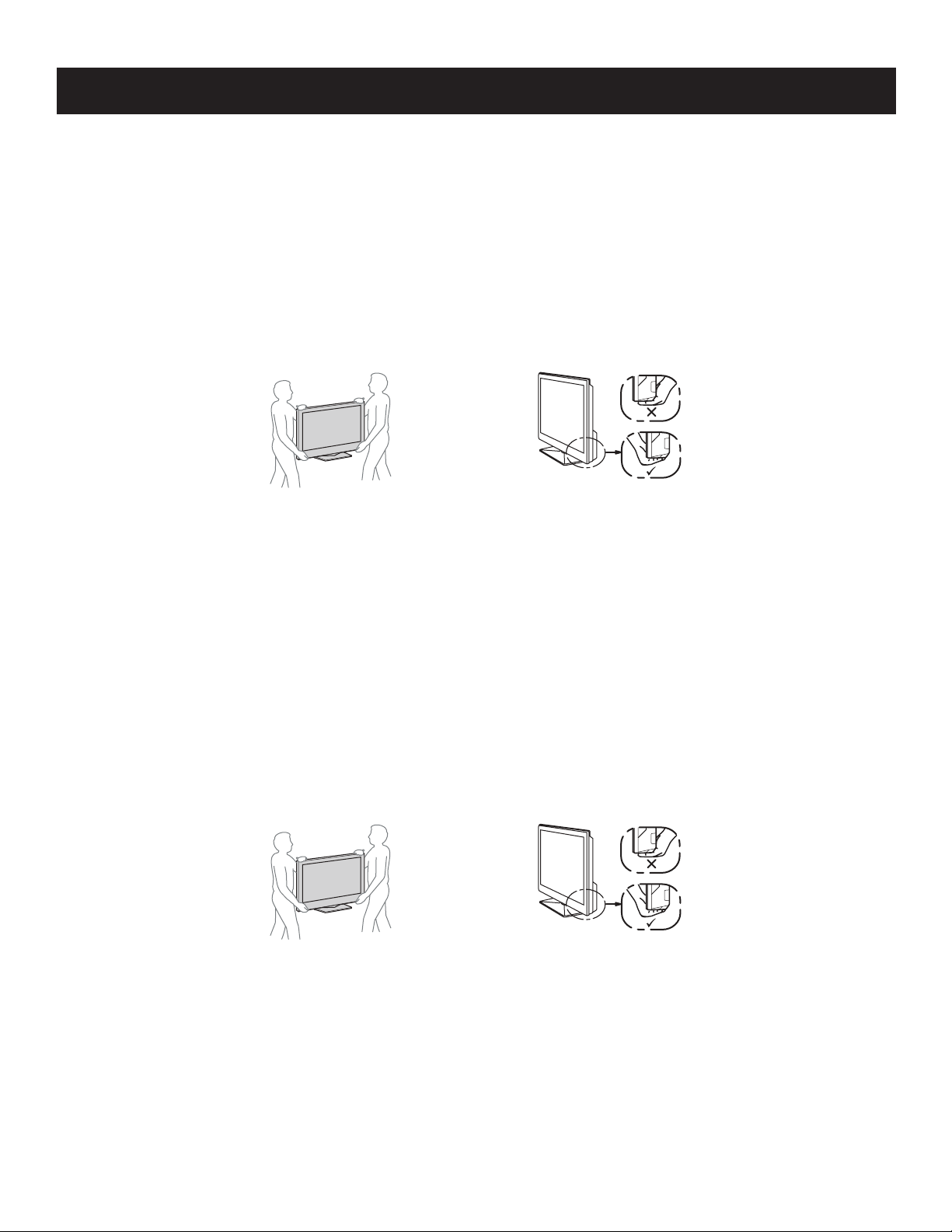
CARRYING THE TV
• Disconnect all cables when carrying the TV.
• Carry the TV with the adequate number of people; larger size TVs require two or more people.
• Correct hand placement while carrying the TV is very important for safety and to avoid damage.
ATTENTION!!
Ces instructions de service sont à l’usage du personnel de service qualié seulement. Pour prévenir le risque de choc
électrique, ne pas faire l’entretien autre que celui contenu dans le Mode d’emploi à moins que vous soyez qualié faire
ainsi.
ALERTE!!
An d’eviter tout risque d’electrocution provenant d’un chássis sous tension, un transformateur d’isolement doit etre utilisé
lors de tout dépannage.
POUR TRANSPORTER LE TÉLÉVISEUR
• Débranchez tous les câbles avant de transporter le téléviseur.
• Transportez le téléviseur avec le nombre adéquat de personnes; téléviseur de grande taille nécessitent deux
personnes ou plus.
• Lors du transport du téléviseur, le bon emplacement des mains est très important pour votre sécurité, ainsi que pour
éviter de causer des dommages.
KDL-32BX330/32BX331
3
KDL-32BX330/32BX331
SAFETY-RELATED WARNING
! SAFETY-RELATED COMPONENT WARNING!!
There are critical components used in LCD color TVs that are important for safety. These components are identied with
shading and ! mark on the schematic diagrams and the electrical parts list. It is essential that these critical parts be
replaced only with the part number specied in the electrical parts list to prevent electric shock, re, or other hazard.
NOTE: Do not modify the original design without obtaining written permission from the manufacturer or you will void the
original parts and labor warranty.
USE CAUTION WHEN HANDLING THE LCD PANEL
When repairing the LCD panel, be sure you are grounded by using a wrist band.
When installing the LCD panel on a wall, the LCD panel must be secured using the 4 mounting holes on the rear
cover.
To avoid damaging the LCD panel:
1) Do not press on the panel or frame edge to avoid the risk of electric shock.
2) Do not scratch or press on the panel with any sharp objects.
3) Do not leave the module in high temperatures or in areas of high humidity for an extended period of
time.
4) Do not expose the LCD panel to direct sunlight.
5) Avoid contact with water. It may cause a short circuit within the module.
6) Disconnect the AC power when replacing the backlight (CCFL) or inverter circuit.
(High voltage occurs at the inverter circuit at 650Vrms.)
7) Always clean the LCD panel with a soft cloth material.
8) Use care when handling the wires or connectors of the inverter circuit. Damaging the wires may cause
a short.
9) Protect the panel from ESD to avoid damaging the electronic circuit (C-MOS).
10) During the repair, DO NOT leave the Power On for more than 1 hour while the TV is face down on a
cloth.
KDL-32BX330/32BX331
4
KDL-32BX330/32BX331
! ATTENTION AUX COMPOSANTS RELATIFS A LA SECURITE!!
Il ya des composants essentiels utilisés dans les téléviseurs LCD couleur qui sont importants pour la sécurité. Ces
composants sont identiés à l’ombrage et ! marque sur les schémas et la liste des pièces électriques. Il est essentiel que
ces parties critiques être remplacé uniquement avec le numéro de pièce gurant dans la liste des pièces électriques pour
éviter les chocs électriques, d’incendie ou autre danger.
NOTE: Ne pas modier la version originale sans obtenir la permission écrite du fabricant ou que vous annulera les pièces
d’origine ainsi que la garantie du travail.
FAITES ATTENTION LORS DE LA MANIPULATION DE L’ÉCRAN ACL
Au moment de réparer l’écran ACL, assurez-vous d’être mis à la terre à l’aide d’un bracelet à cet effet.
Au moment d’installer le panneau ACL sur un mur, il doit être maintenant en place à l’aide des 4 orices de xation
présents au couvercle arrière.
Pour éviter d’endommager l’écran LCD:
1) N’appuyez par sur le bord du panneau ou du cadre an d’éviter le risque de choc électrique.
2) Ne rayez pas ou n’appuyez pas sur le panneau avec des objets pointus.
3) Ne laissez pas le module exposé à des températures élevées ou dans des secteurs à haut niveau
d’humidité pour une période prolongée.
4) N’exposez pas le panneau ACL à l’ensoleillement direct.
5) Évitez le contact avec l’eau, car elle peut causer un court-circuit dans le module.
6) Déconnectez l’alimentation c.a. au moment de remplacer le rétroéclairage ou le circuit inverseur (Un
voltage élevé se produit dans le circuit inverseur à 650Vrms).
7) Nettoyez toujours le panneau ACL avec un chiffon doux.
8) Faites attention lors de la manipulation des ls ou connecteurs du circuit inverseur. Le fait
d’endommager les lms peut causer un court-circuit.
9) Protégez le panneau des décharges électrostatiques an d’éviter d’endommager le circuit électronique
(C-MOS).
10) Pendant la réparation, NE LAISSEZ PAS l’alimentation en fonction pendant plus de 1 heure pendant
que l’écran du téléviseur repose sur un tissu.
KDL-32BX330/32BX331
5
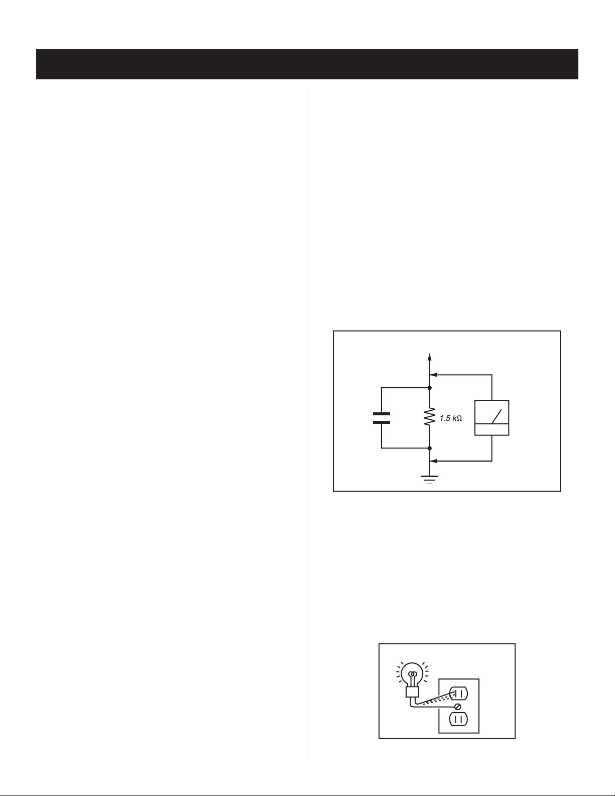
SAFETY CHECK-OUT
To Exposed Metal
Parts on Set
0.15 µF
Earth Ground
AC
Voltmete
r
(0.75V)
Trouble Light
KDL-32BX330/32BX331
After correcting the original service problem, perform the
following safety checks before releasing the set to the
customer:
1) Check the area of your repair for unsoldered
or poorly soldered connections. Check the
entire board surface for solder splashes and
bridges.
2) Check the interboard wiring to ensure that no
wires are “pinched” or touching high-wattage
resistors.
3) Check that all control knobs, shields, covers,
ground straps, and mounting hardware have
been replaced. Be absolutely certain that you
have replaced all the insulators.
4) Look for unauthorized replacement parts,
particularly transistors, that were installed
during a previous repair. Point them out
to the customer and recommend their
replacement.
5) Look for parts which, though functioning,
show obvious signs of deterioration. Point
them out to the customer and recommend
their replacement.
6) Check the line cords for cracks and abrasion.
Recommend the replacement of any such
line cord to the customer.
7) Check the antenna terminals, metal trim,
“metallized” knobs, screws, and all other
exposed metal parts for AC leakage. Check
leakage as described in “Leakage Test”.
LEAKAGE TEST
The AC leakage from any exposed metal part to earth
ground and from all exposed metal parts to any exposed
metal part having a return to chassis, must not exceed
0.5 mA (500 microamperes). Leakage current can be
measured by any one of three methods.
1. A commercial leakage tester. Follow the
manufacturers’ instructions provided with the
tester.
2. A battery-operated AC milliammeter.
3. Measuring the voltage drop across a resistor
by means of a VOM or battery-operated AC
voltmeter. The “limit” indication is 0.75 V, so
analog meters must have an accurate low
voltage scale. Nearly all battery-operated
digital multimeters that have a 2 VAC range
are suitable. (see Figure A)
Figure A. Use an AC voltmeter to check AC leakage.
KDL-32BX330/32BX331
HOW TO FIND A GOOD EARTH GROUND
The cover-plate retaining screw on most AC outlet boxes
is at earth ground. Verify the AC outlet box retaining screw
ground by connecting a 60W to 100W incandescent (not
a neon lamp or uorescent lamp) between the hot side
of the receptacle and the retaining screw. Try both slots,
if necessary, to locate the hot side on the line; the lamp
should light at normal brilliance if the screw is at ground
potential. (see Figure B)
AC Outlet Box
Figure B. Checking for earth ground.
6
KDL-32BX330/32BX331
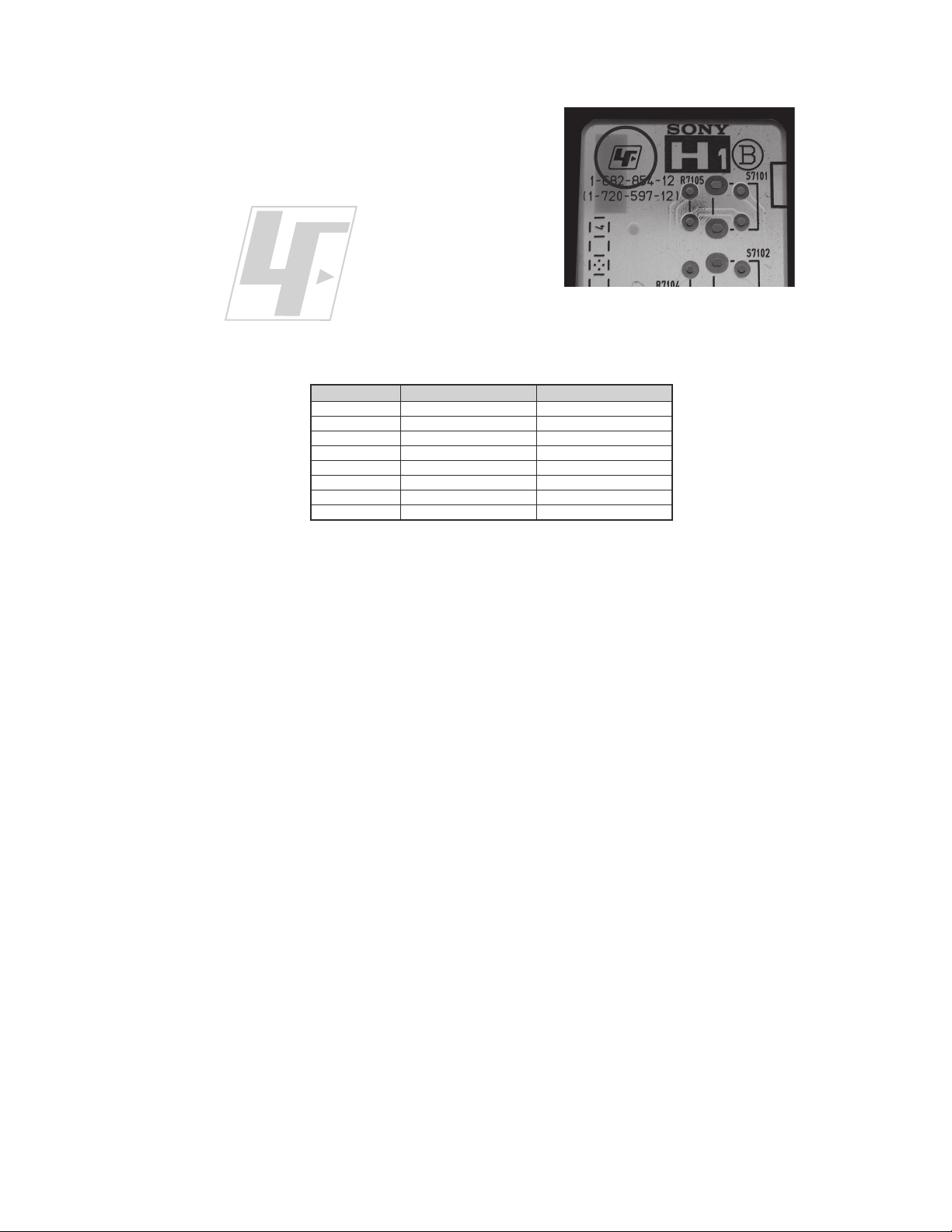
Th
e circuit boards used in these models have been processed using
Lead Free Solder. The boards are identified by the LF logo located
close to the board designation e.g. H1 etc [ see example ]. The
servicing of these boards requires special precautions to be taken as
outlined below.
example
It is strongly recommended to use Lead Free Solder material in order to guarantee optimal quality of new solder joints.
Lead Free Solder is available under the following part numbers :
rebmuntraP retemaiD skrameR
91-500-046-7mm3.0gK52.0
02-500-046-7mm4.0gK05.0
12-500-046-7mm5.0gK05.0
22-500-046-7mm6.0gK52.0
32-500-046-7mm8.0gK00.1
42-500-046-7mm0.1gK00.1
52-500-046-7mm2.1gK00.1
62-500-046-7mm6.1gK00.1
Due to the higher melting point of Lead Free Solder the soldering iron tip temperature needs to be set to 370 degrees celsius.
This requires soldering equipment capable of accurate temperature control coupled with a good heat recovery characteristics.
KDL-32BX330/32BX331
7
KDL-32BX330/32BX331
Model name KDL-32BX330 KDL-32BX331
FEATURES AND SPECIFICATIONS
FEATURES
Impressive clarity
Perfect for the bedroom or ofce, 720p image resolution delivers pristine picture quality wherever you need it. Watch movies, sports and primetime HD
television broadcasts with robust detail that is optimized for 16:9 widescreen panels (1366 x 768) and modest screen sizes.
Four HD inputs
Plug into the action with versatile HD connection options. Four HD inputs include two HDMI® inputs for sources like your HD cable box, home theater
system, Blu-ray Disc™ player or PS3™ system, one HD component input and a PC input (HD-15 pin) which lets you use your HDTV as a computer
monitor.
USB input for your camera and more
Share your vacation photos instantly on the big screen or listen to your favorite music. Simply connect your compatible digital camera, USB-enabled
MP3 player or USB storage device directly to your HDTV’s USB input. It’s a fast and simple way to relive the memories without a hassle.
Against the grain
Dazzle the whole family with ultra-crisp HD clarity and less grain. Digital Noise Reduction enhances detail in whatever you’re watching with meticulous
processing. It even helps clean up video from USB and other PC sources so the picture looks pristine and vivid.
SPECIFICATIONS
System
Television system NTSC: American TV standard
Channel coverageAnalog terrestrial: 2 - 69 / Digital terrestrial: 2 - 69
Panel system LCD (Liquid Crystal Display) Panel
ATSC (8VSB terrestrial): ATSC compliant 8VSB
QAM on cable: ANSI/SCTE 07 2000 (Does not include CableCARD functionality)
Analog Cable: 1 - 135 / Digital Cable: 1 - 135
Input/Output jacks
CABLE/ANTENNA 75-ohm external terminal for RF inputs
COMPONENT IN YP
HDMI IN 1/2 HDMI: Video: 480i, 480p, 720p, 1080i, 1080p, 1080/24p
DIGITAL AU DIO OUT
(OPTICAL)
AUDIO OUT (FIX) Stereo mini jack, 500 mVrms, (Typical)
PC/HDMI IN 1 AUDIO INPUT Stereo mini jack, 500 mVrms, (Typical) / Impedance: 47 kilohms
AUDIO: 500 mVrms (Typical) / Impedance: 47 kilohms
BPR (Component Video): Y: 1.0 Vp-p, 75 ohms unbalanced, sync negative / PB : 0.7 Vp-p, 75 ohms
R : 0.7 Vp-p, 75 ohms / Signal format: 480i, 480p, 720p, 1080i, 1080p
P
AUDIO: 500 mVrms (Typical) / Impedance: 47 kilohms
Audio: Two channel linear PCM 32, 44.1 and 48 kHz, 16, 20 and 24bits, Dolby Digital
PC Input (see page 35)
PCM/Dolby Digital optical signal
See the PC Input Signal Reference Chart for PC and HDMI IN in the Operating Instructions manual.
Power and others
Power requirement120 V AC, 60 Hz
Power consumption
in use
in standbyLess than 0.3 W with 120 V AC
Screen size
(inches measured diagonally)
Speaker/Full range (2) (mm)
Dimensions with stand (mm)
wall-mount hole pattern (mm)
Mass with stand (kg)
Supplied accessories Remote control RM-YD072 (1)/Size AA batter ies (2)/Operating Instructions (1)/Quick Setup Guide
Optional accessoriesConnecting cables / Wall-Mount Bracket: SU-WL500
•Optional accessories availability depends on stock.
•Design and specications are subject to change without notice.
(inches)
(inches)
without stand (mm)
without stand (kg)
(inches)
(lb.)
(lb.)
(1)/Warranty Card (1)/Safety and Regulatory Booklet (1)/Software License (1)/Stand installation
guide (1)/Table-Top Stand (1)/Screw (3)/Attachment Parts (2)
KDL-32BX330/32BX331
evitagen cnys ,decnalabnu smho 57 ,p-pV 1 :OEDIVNI OEDIV
84 W
31.5
(32 class)
30 × 100
1
/5 × 4)
(1
772 × 526 × 207
1
30
/2 × 20 3/4 × 8 1/4
772 × 484 × 82
1
30
/2 × 19 1/8 × 3 1/
200 × 300
6.3
13.9
5.8
12.8
W 8 + W 8 W 6 + W 6 tuptuo rekaepS
evitisop ,smho 57 ,p-pV 7.0 ,BGR golana ,nip-51 bus-DNI CP
GEPJ3PM ,GEPJBSU
)lacitrev( senil 867 × )latnoziroh( stod 883,1 noituloser yalpsiD
4
m in the Operating Instructions manual.)argaid ot refer :htgnel( 6M)mm( ezis wercs tnuom-llaw
8
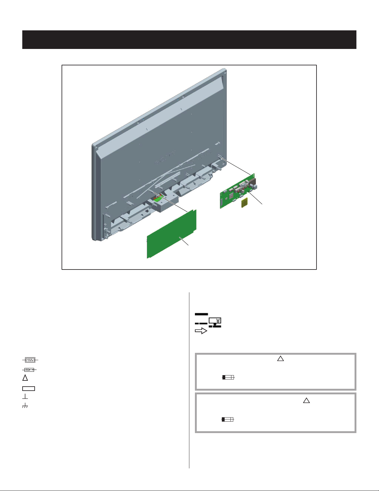
1-1. CIRCUIT BOARDS LOCATION
KDL-32BX330/32BX331
SECTION 1: DIAGRAMS
A Board
Power Supply Board
1-2. PRINTED CIRCUIT BOARDS AND SCHEMATIC DIAGRAMS INFORMATION
All capacitors are in µF unless otherwise noted. pF : µµF 50WV or
less are not indicated except for electrolytics and tantalums.
All electrolytics are in 50V unless otherwise specied.
All resistors are in ohms. kΩ=1000Ω, MΩ=1000kΩ
Indication of resistance, which does not have one for rating
electrical power, is as follows: Pitch : 5mm
Rating electrical power :
1
/
W in resistance, 1/
4
W and 1/
10
W in chip resistance.
16
1
/
4
: nonammable resistor
: fusible resistor
: internal component
: panel designation and adjustment for repair
: earth ground
: earth-chassis
All variable and adjustable resistors have characteristic curve B,
unless otherwise noted.
Readings are taken with a color-bar signal input.
Readings are taken with a 10MΩ digital multimeter.
Voltages are DC with respect to ground unless otherwise noted.
Voltage variations may be noted due to normal production
tolerances.
KDL-32BX330/32BX331
All voltages are in V.
S : Measurement impossibility.
: B+line.
: B-line. (Actual measured value may be different).
: signal path. (RF)
Circled numbers are waveform references.
W
The components identied by shading and ! symbol are critical for safety. Replace
only with part number specied.
The symbol indicates a fast-blow fuse and is displayed on the component
side of the board. Replace only with fuse of the same rating as marked.
Les composants identies per un trame et une marque
securite. Ne les remplacer que par une piece portant le numero specie.
Le symbole indique une fusible a action rapide. Doit etre remplace par une
fusible de meme yaleur, comme maque.
!
sont critiques pour la
9
1-3. SCHEMATICS AND SUPPORTING INFORMATION
A BOARD SCHEMATIC DIAGRAM (1 OF 14)
5
U100A
U100A
ZR39748BGCG
ZR39748BGCG
S0 Memory I/F
D D
C C
S0_DQ15
S0_DQ14
S0_DQ13
S0_DQ12
S0_DQ11
S0_DQ10
S0_DQ9
S0_DQ8
S0_DQ7
S0_DQ6
S0_DQ5
S0_DQ4
S0_DQ3
S0_DQ2
S0_DQ1
S0_DQ0
S0_UDM
S0_LDM
AA15
AA9
AA16
AB9
AB11
AB14
AA10
AB16
AA13
AA8
AB12
AA7
AB7
AA12
AB8
AB13
AB10
AA11
V13
V17
U17
V16
S0 Memory I/F
S0DAT15
S0DAT14
S0DAT13
S0DAT12
S0DAT11
S0DAT10
S0DAT9
S0DAT8
S0DAT7
S0DAT6
S0DAT5
S0DAT4
S0DAT3
S0DAT2
S0DAT1
S0DAT0
S0DQM1
S0DQM0
S0VREF
RDRIVER
RDRIVER50
RTERM
null
null
DRAM POWER DDRV
VCC1_8
L100
B B
L100
120R-100MHZ_0805
120R-100MHZ_0805
C100
C100
22U_6.3V_M
22U_6.3V_M
0805_X5R
0805_X5R
1 2
DDR_VCC1_8
12
C101
C101
0.1U_10V_K
0.1U_10V_K
0402_X7R
0402_X7R
1
TP100TP100
DDR_VCC1_8
12
C103
C103
1000P_50V_K
1000P_50V_K
0402_X7R
0402_X7R
4
S0ADR12
S0ADR11
S0ADR10
S0ADR9
S0ADR8
S0ADR7
S0ADR6
S0ADR5
S0ADR4
S0ADR3
S0ADR2
S0ADR1
S0ADR0
S0BS2
S0BS1
S0BS0
S0DQS1N
S0DQS1P
S0DQS0N
S0DQS0P
S0RASN
S0CASN
S0WEN
S0CLKN
S0CLKP
S0CKE
S0ODT
12
AB1
Y22
AB4
AA1
AA22
AB2
AB22
AA2
AA21
AB3
AB21
AA3
AA20
AA5
AA4
AB5
AB15
AA14
AB17
AA17
AA19
AB20
AB6
AA18
AB18
AA6
AB19
C104
C104
0.1U_10V_K
0.1U_10V_K
0402_X7R
0402_X7R
1 2
S0_ODT
12
C105
C105
0.1U_10V_K
0.1U_10V_K
0402_X7R
0402_X7R
S0_A12
S0_A11
S0_A10
S0_A9
S0_A8
S0_A7
S0_A6
S0_A5
S0_A4
S0_A3
S0_A2
S0_A1
S0_A0
S0_BA2
S0_BA1
S0_BA0
S0_UDQSN
S0_UDQS
S0_LDQSN
S0_LDQS
S0_RASN
S0_CASN
S0_WEN
S0_CKN
S0_CK
S0_CKE
R102
R102
100_F 0603
100_F 0603
Place under U101
12
C106
C106
0.1U_10V_K
0.1U_10V_K
0402_X7R
0402_X7R
Place R102
close to U101
12
C107
C107
0.1U_10V_K
0.1U_10V_K
0402_X7R
0402_X7R
12
3
DDR_VCC1_8
C108
C108
0.1U_10V_K
0.1U_10V_K
0402_X7R
0402_X7R
R100
R100
100_F 0603
100_F 0603
1 2
C109
C109
22U_6 3V_M
22U_6 3V_M
0805_X5R
0805_X5R
1 2
12
R101
R101
100_F
100_F
0603
0603
S0_UDQS
S0_UDQSN
S0_LDQS
S0_LDQSN
S0_UDM
S0_LDM
DDR_VCC1_8
S0_DQ0
S0_DQ1
S0_DQ2
S0_DQ3
S0_DQ4
S0_DQ5
S0_DQ6
S0_DQ7
S0_DQ8
S0_DQ9
S0_DQ10
S0_DQ11
S0_DQ12
S0_DQ13
S0_DQ14
S0_DQ15
2
U101
U101
G8
DQ0
G2
DQ1
H7
DQ2
H3
DQ3
H1
DQ4
H9
DQ5
F1
DQ6
F9
DQ7
C8
DQ8
C2
DQ9
D7
DQ10
D3
DQ11
D1
DQ12
D9
DQ13
B1
DQ14
B9
DQ15
A2
NC_1
E2
NC_2
B7
UDQS
A8
UDQS#
F7
LDQS
E8
LDQS#
B3
UDM
F3
LDM
J2
VREF
K2
CKE
A1
VDD_1
A9
VDDQ_1
C1
VDDQ_2
C3
VDDQ_3
C7
VDDQ_4
C9
VDDQ_5
E1
VDD_2
E9
VDDQ_6
G1
VDDQ_7
G3
VDDQ_8
G7
VDDQ_9
G9
VDDQ_10
J1
VDDL
J9
VDD_3
VDD_4M9VSS_4
R1
VDD_5
SDRAM_BGA-84P_512MB
SDRAM_BGA-84P_512MB
NT5TU32M16DG-BD
NT5TU32M16DG-BD
A10/AP
VSSQ_1
VSSQ_2
VSSQ_3
VSSQ_4
VSSQ_5
VSSQ_6
VSSQ_7
VSSQ_8
VSSQ_9
VSSQ_10
A11
A12
NC_6
NC_4
NC_5
BA0
BA1
NC_3
CK
CK#
CS#
CAS#
ODT
RAS#
WE#
VSS_1
VSS_2
VSS_3
VSSDL
VSS_5
1
M8
A0
M3
A1
M7
A2
N2
A3
N8
A4
N3
A5
N7
A6
P2
A7
P8
A8
P3
A9
M2
P7
R2
R8
R3
R7
L2
L3
L1
J8
K8
L8
L7
K9
K7
K3
A3
A7
B2
B8
D2
D8
E3
E7
F2
F8
H2
H8
J3
J7
N1
P9
S0_A0
S0_A1
S0_A2
S0_A3
S0_A4
S0_A5
S0_A6
S0_A7
S0_A8
S0_A9
S0_A10
S0_A11
S0_A12
S0_BA0
S0_BA1
S0_BA2
S0_CK
S0_CKN
S0_CASN
S0_ODT
S0_RASN
S0_WENS0_CKE
KDL-32BX330/32BX331
DDR_VCC1_8
12
C117
C117
0.1U_10V_K
0.1U_10V_K
0402_X7R
0402_X7R
12
C111
C111
0.1U_10V_K
0.1U_10V_K
0402_X7R
0402_X7R
4
12
C110
C110
1000P_50V_K
1000P_50V_K
0402_X7R
0402_X7R
DDR_VCC1_8
A A
5
12
C118
C118
0.1U_10V_K
0.1U_10V_K
0402_X7R
0402_X7R
12
C112
C112
1000P_50V_K
1000P_50V_K
0402_X7R
0402_X7R
12
C119
C119
0.1U_10V_K
0.1U_10V_K
0402_X7R
0402_X7R
12
C113
C113
0.1U_10V_K
0.1U_10V_K
0402_X7R
0402_X7R
12
C114
C114
1000P_50V_K
1000P_50V_K
0402_X7R
0402_X7R
12
C115
C115
0.1U_10V_K
0.1U_10V_K
0402_X7R
0402_X7R
3
C116
C116
22U_6 3V_M
22U_6 3V_M
0805_X5R
0805_X5R
1 2
TV Product Business Division / R&D Department
TV Product Business Division / R&D Department
TV Product Business Division / R&D Department
CCPBG/ Hon-Hai Precision IND. CO., LTD
CCPBG/ Hon-Hai Precision IND. CO., LTD
CCPBG/ Hon-Hai Precision IND. CO., LTD
Foxconn Technology Group
Foxconn Technology Group
Title
Title
Title
DDR2
DDR2
DDR2
Size Document Number Rev
Size Document Number Rev
Size Document Number Rev
B
B
B
TINA1
TINA1
TINA1
Date: Sheet
Date: Sheet
2
Date: Sheet
Foxconn Technology Group
2 16Friday, June 24, 2011
2 16Friday, June 24, 2011
2 16Friday, June 24, 2011
1
of
of
of
KDL-32BX330/32BX331
9
9
9
10
KDL-32BX330/32BX331
A BOARD SCHEMATIC DIAGRAM (2 OF 14)
5
U100B
U100B
ZR39748BGCG
ZR39748BGCG
D D
EJTAG
EJTAG
UART
UART
I2C
I2C
C C
SPI
SPI
25M
25M
null
null
USB2.0
B B
A A
USB2.0
SIO I/F
SIO I/F
5
TDI
TDO
TMS
TCK
UART1TX
UART1RX
I2C0C
I2C0D
I2C1C
I2C1D
SPI_DO
SPI_DI
SPI_CLK
SPI_SEL0
SPI_SEL1
SPI_HOLD
CLKOUT_25M
CLKIN_25M
USB_DN
USB_DP
USB_REXT
USB_ATEST
D19
D18
C18
D20
F20
E20
F4
F3
A21
A22
C22
B22
B21
C21
Y21
C20
A8
B8
W21
W22
T18
V19
EJTDI
EJTD0
EJTMS
EJTCK
R185
R185
100_F 0402
100_F 0402
1 2
1 2
R184
NC/100_F
NC/100_F
1 2
R190 100_F 0402R190 100_F 0402
R191
1 2
100_F
100_F
D157 EZAEG2A50AX_VR
D157 EZAEG2A50AX_VR
D158 EZAEG2A50AX_VR
D158 EZAEG2A50AX_VR
R182 100_F0402R182 100_F0402
1 2
1 2
R183 100_F0402R183 100_F0402
C151
C151
12P_50V_J
12P_50V_J
0402_NPO
0402_NPO
1 2
VSW_CPR
0402R184
0402
I2C_0_SCL
I2C_0_SDA
I2C_1_SCL
0402R191
0402
I2C_1_SDA
1 2
1 2
null
null
null
null
1 2
R166 100_F0402R166 100_F0402
Y150
Y150
B
12
A
25MHZ_6.3P_15PPM
25MHZ_6.3P_15PPM
SONY_1-814-389-11
SONY_1-814-389-11
R167
R167
6 04K_F
6 04K_F
0402
0402
10U_10V_M
10U_10V_M
0805_X5R
0805_X5R
VCC3_3
RESETN[5,8,11]
VCC_ERR_DET
VSW_CY_DET
D
C
12
C156
C156
R172
R172
1 2
10K_J
10K_J
0402
0402
4
VCC3_3
R150 NC/0_F0402R150 NC/0_F0402
1 2
1 2
R151 NC/0_F0402R151 NC/0_F0402
1 2
R152 NC/0_F0402R152 NC/0_F0402
1 2
R153 NC/0_F0402R153 NC/0_F0402
1 2
R154 NC/47_J0402R154 NC/47_J0402
1
Close to U100
TP151TP151
TP150TP150
1
1 2
R161 4.7K_J0402R161 4.7K_J0402
1 2
R162 4.7K_J0402R162 4.7K_J0402
1 2
R159 4.7K_J0402R159 4.7K_J0402
R160 4.7K_J0402R160 4.7K_J0402
1 2
SPI_WR
SPI_RD
SPI_CLK
SPI_CS_n
Close to U100
Crystal Y1
12
C152
C152
12P_50V_J
12P_50V_J
0402_NPO
0402_NPO
50ppm 0-70C
Add a GROUND guard
to avoid ESD
nullU151
null
USB POWER
4
VIN
GND2FLG#
3
CHANGE TO CURRENT LIMIT TO 0.5A
12
C153
C153
0.1U_10V_K
0.1U_10V_K
0402_X7R
0402_X7R
U151
FP6861S5GTR
FP6861S5GTR
USB_OC_N
4
VCC3_3
5
VOUT
EN
1
12
C157
C157
1206_X5R
1206_X5R
47U_6.3V_M
47U_6.3V_M
USB_PEN_N
3
R158
R158
R157
R156
R156
1 2
12
12
1206_X5R
1206_X5R
R157
1 2
1 2
12
12
VCC3_3
R163
R163
0_J 0603
0_J 0603
1 2
1 2
R171
0_J
0_J
12
C155
C155
0.1U_10V_K
0.1U_10V_K
0402_X7R
0402_X7R
Close to CN151
NC/4.7K_J0402
NC/4.7K_J0402
NC/1K_J0402
NC/1K_J0402
NC/1K_J0402
NC/1K_J0402
12
0603R171
0603
VCC5_1_USBVCC5_0_USB
3
R155 NC/1K_J0402R155 NC/1K_J0402
1 2
12
D150 NC/EZAEG2A50AX_VR nullD150 NC/EZAEG2A50AX_VR null
D151 NC/EZAEG2A50AX_VR nullD151 NC/EZAEG2A50AX_VR null
D152 NC/EZAEG2A50AX_VR nullD152 NC/EZAEG2A50AX_VR null
D153 NC/EZAEG2A50AX_VR nullD153 NC/EZAEG2A50AX_VR null
D154 NC/EZAEG2A50AX_VR nullD154 NC/EZAEG2A50AX_VR null
12
C154
C154
47U_6.3V_M
47U_6.3V_M
1206_X5R
1206_X5R
C158 47U_6.3V_M
C158 47U_6.3V_M
VCC3_3
UART0_RX
UART0_TX
1
2
3
4
5
6
7
8
9
CN150
CN150
SMDFIX2
SMDFIX2
NC/HEADER CONN_9P
NC/HEADER CONN_9P
FOX_HS7209E
FOX_HS7209E
SMDFIX1
SMDFIX1
10 11
For Development Only
Close to CN150
U150
U150
R164
R164
NC/4.7K_J
NC/4.7K_J
0402
0402
12
D155
D155
null
null
SPI_CS_n
SPI_RD
12
R165
R165
4.7K_J
4.7K_J
0402
0402
1 2
VCC5_1_USB
12
D156
D156
null
null
EZAEG2A50AX_VR
EZAEG2A50AX_VR
EZAEG2A50AX_VR
EZAEG2A50AX_VR
1
S#
2
Q
3
W#/VPP
4
VSS
FLASH_SO8W- 8P_32MBIT
FLASH_SO8W- 8P_32MBIT
W25Q32BVSSI G
W25Q32BVSSI G
Near of U100
L151
L151
100R-100MHZ_0805
100R-100MHZ_0805
VCC
HOLD#
8
7
6
C
5
D
2
1 2
1
V-
V-
2
V+
V+
3
4
2
R170
R170
4.7K_J 0402
4.7K_J 0402
SPI_CLK
SPI_WR
56
78
PTH1
PTH3
PTH1
PTH3
VCC
VCC
GND
GND
PTH2PTH4
PTH2PTH4
1
UART0_TX
UART0_RX
USB_OC_N
USB_PEN_N
I2C_0_SCL
I2C_0_SDA
I2C_1_SCL
I2C_1_SDA
VSW_CY_DET
VSW_CPR
VCC3_3
12
C150
C150
0.1U_10V_K
0.1U_10V_K
0402_X7R
0402_X7R
3/28 Change the USB connect or
from 2N-000400D-F KG0 to 2N-0004016-MKG0.
Jack.
CN151
CN151
USB CONN_4P
USB CONN_4P
FOX_UB11121-4GD1-4F
FOX_UB11121-4GD1-4F
TV Product Business Division / R&D Department
TV Product Business Division / R&D Department
TV Product Business Division / R&D Department
CCPBG/ Hon-Hai Precision IND. CO., LTD
CCPBG/ Hon-Hai Precision IND. CO., LTD
CCPBG/ Hon-Hai Precision IND. CO., LTD
Foxconn Technology Group
Foxconn Technology Group
Title
Title
Title
SIO I/F
SIO I/F
SIO I/F
Size Document Number Rev
Size Document Number Rev
Size Document Number Rev
B
B
B
TINA1
TINA1
TINA1
Date: Sheet
Date: Sheet
Date: Sheet
Foxconn Technology Group
UART0_TX [6,11]
UART0_RX [6,11]
USB_OC_N [10]
USB_PEN_N [10]
I2C_0_SCL [11]
I2C_0_SDA [11]
I2C_1_SCL [5,8,9]
I2C_1_SDA [5,8,9]
VSW_CY_DET [6]
VSW_CPR [6]
UART0_TX
UART0_RX
1 2
1 2
3 16Friday, June 24, 2011
3 16Friday, June 24, 2011
3 16Friday, June 24, 2011
1
R168
4.7K_J
4.7K_J
R169
4.7K_J
4.7K_J
of
of
of
VCC3_3
0402R168
0402
0402R169
0402
9
9
9
KDL-32BX330/32BX331
11
KDL-32BX330/32BX331
A BOARD SCHEMATIC DIAGRAM (3 OF 14)
5
CN200
CN200
HDMI CONN_19P
HDMI CONN_19P
CEC
ARC
SCL
SDA
VCC5
HPD
1
2
3
4
5
6
7
8
9
10
11
12
13
14
15
16
17
18
19
20
21
22
23
24
TMDSD2+
DSHLD2
TMDSD2-
TMDSD1+
D D
C C
SONY_1-822-482-11
SONY_1-822-482-11
DSHLD1
TMDSD1-
TMDSD0+
DSHLD0
TMDSD0-
TMDSDC+
DSHLDC
TMDSDC-
DDC_GND
SWITCH
SH ELD1
SH ELD2
SH ELD3
SH ELD4
HDMI0_D2P
HDMI0_D2N
HDMI0_D1P
HDMI0_D1N
HDMI0_D0P
HDMI0_D0N
HDMI0_CLKP
HDMI0_CLKN
HDMI_CEC
HDMI0_ARC
HDMI0_DDC_SCL
HDMI0_DDC_SDA
HDMI0_5V
1 2
R203
1K_J
1K_J
HDMI0_DDC_SCL
HDMI0_DDC_SDA
HPD0
HDMI0_5V
HDMI0_HPDHPD0
0402R203
0402
1 2
1 2
1 2
1 2
HDMI0_5V
4
R200 47K_J 0402R200 47K_J 0402
R201 47K_J 0402R201 47K_J 0402
1 2
12
R218
R218
10K_J
10K_J
0402
0402
D200 NC/EZAEG2A50AX_VR nullD200 NC/EZAEG2A50AX_VR null
D201 NC/EZAEG2A50AX_VR nullD201 NC/EZAEG2A50AX_VR null
D202 NC/EZAEG2A50AX_VR nullD202 NC/EZAEG2A50AX_VR null
D203 EZAEG2A50AX_VR nullD203 EZAEG2A50AX_VR null
12
C200
C200
0.1U_10V_K
0.1U_10V_K
0402_X7R
0402_X7R
1 2
HDMI0_DDC_SCL
HDMI0_DDC_SDA
Close to CN200
IEC958_O
R212
R212
NC_100_F0402
NC_100_F0402
1 2
3
HDMI_CEC
1
R213
R213
NC/100_F
NC/100_F
0402
0402
VCC3_3_STB
1 2
R217
R217
27K_J
27K_J
0402
0402
1 2
HDMI0_5V
C
C
B
B
E
E
2 3
1 2
12
1
D212
D212
RB751V-40
RB751V-40
null
null
Q201
Q201
LMBT3904LT1G
LMBT3904LT1G
R214
R214
NC/33_J
NC/33_J
0402
0402
HDMI_CEC_IN
S
S
G
G
Q200
Q200
NC/2N7002
NC/2N7002
null
null
D
D
3 2
1 2
C203
C203
NC/1U_10V_K
NC/1U_10V_K
0402_X5R
0402_X5R
12
R216
R216
NC/740_F
NC/740_F
0402
0402
HDMI0_ARC
12
R215
R215
NC/100_F
NC/100_F
0402
0402
2
HDMI0_D2P
HDMI0_D2N
HDMI0_D1P
HDMI0_D1N
HDMI0_D0P
HDMI0_D0N
HDMI0_CLKP
HDMI0_CLKN
HDMI1_D2P
HDMI1_D2N
HDMI1_D1P
HDMI1_D1N
HDMI1_D0P
HDMI1_D0N
HDMI1_CLKP
HDMI1_CLKN
U100C
U100C
ZR39748BGCG
ZR39748BGCG
Y2
HDM 0_D2P
Y1
HDM 0_D2N
W2
HDM 0_D1P
W1
HDM 0_D1N
V2
HDM 0_D0P
V1
HDM 0_D0N
U2
HDM 0_CP
U1
HDM 0_CN
T2
HDMI1_D2P
T1
HDMI1_D2N
R2
HDMI1_D1P
R1
HDMI1_D1N
P2
HDMI1_D0P
P1
HDMI1_D0N
N2
HDMI1_CP
N1
HDMI1_CN
M2
HDMI2_D2P
M1
HDMI2_D2N
L2
HDMI2_D1P
L1
HDMI2_D1N
K2
HDMI2_D0P
K1
HDMI2_D0N
J2
HDMI2_CP
J1
HDMI2_CN
1
HDMI I/F
HDMI I/F
null
CN201
CN201
HDMI CONN_19P
HDMI CONN_19P
CEC
ARC
SCL
SDA
VCC5
HPD
1
2
3
4
5
6
7
8
9
10
11
12
13
14
15
16
17
18
19
20
21
22
23
24
TMDSD2+
DSHLD2
B B
A A
SONY_1-822-482-11
SONY_1-822-482-11
TMDSD2-
TMDSD1+
DSHLD1
TMDSD1-
TMDSD0+
DSHLD0
TMDSD0-
TMDSDC+
DSHLDC
TMDSDC-
DDC_GND
SWITCH
SH ELD1
SH ELD2
SH ELD3
SH ELD4
HDMI1_D2P
HDMI1_D2N
HDMI1_D1P
HDMI1_D1N
HDMI1_D0P
HDMI1_D0N
HDMI1_CLKP
HDMI1_CLKN
HDMI_CEC
HDMI1_DDC_SCL
HDMI1_DDC_SDA
HDMI1_5V
HPD1
HDMI1_DDC_SCL
HDMI1_DDC_SDA
HPD1
HDMI1_5V
Close to CN201
1 2
R207
0402R207
0402
1K_J
1K_J
HDMI1_5V
HDMI1_HPD
1 2
1 2
1 2
1 2
12
R219
R219
10K_J
10K_J
0402
0402
All HDMI connectors are mounted as vertical codition
5
R204 47K_J 0402R204 47K_J 0402
R205 47K_J 0402R205 47K_J 0402
1 2
1 2
12
C201
C201
0.1U_10V_K
0.1U_10V_K
0402_X7R
0402_X7R
D204 NC/EZAEG2A50AX_VR nullD204 NC/EZAEG2A50AX_VR null
D205 NC/EZAEG2A50AX_VR nullD205 NC/EZAEG2A50AX_VR null
D206 NC/EZAEG2A50AX_VR nullD206 NC/EZAEG2A50AX_VR null
D207 EZAEG2A50AX_VR nullD207 EZAEG2A50AX_VR null
4
HDMI1_DDC_SCL
HDMI1_DDC_SDA
HDMI0_DDC_SCL
HDMI0_DDC_SDA
HDMI0_5V
HDMI0_HPD
HDMI1_DDC_SCL
HDMI1_DDC_SDA
HDMI1_5V
HDMI1_HPD
HDMI_CEC_IN
IEC958_O
TV Product Business Division / R&D Department
TV Product Business Division / R&D Department
TV Product Business Division / R&D Department
CCPBG/ Hon-Hai Precision IND. CO., LTD
CCPBG/ Hon-Hai Precision IND. CO., LTD
CCPBG/ Hon-Hai Precision IND. CO., LTD
Foxconn Technology Group
Foxconn Technology Group
Title
Title
Title
HDMI I/F
HDMI I/F
HDMI I/F
Size Document Number Rev
Size Document Number Rev
Size Document Number Rev
B
B
B
TINA1
TINA1
TINA1
Date: Sheet
Date: Sheet
3
2
Date: Sheet
Foxconn Technology Group
null
HDMI0_DDC_SCL [11]
HDMI0_DDC_SDA [11]
HDMI0_5V [11]
HDMI0_HPD [11]
HDMI1_DDC_SCL [11]
HDMI1_DDC_SDA [11]
HDMI1_5V [11]
HDMI1_HPD [11]
HDMI_CEC_ N [11]
IEC958_O [8]
4 16Friday, June 24, 2011
4 16Friday, June 24, 2011
4 16Friday, June 24, 2011
of
of
of
1
9
9
9
KDL-32BX330/32BX331
12
 Loading...