

HISTORY
Model Name :
SERVICE MANUAL
Click on Page Number to display detail of changes.
Date Part Number Description of Revisions
Original Manual.
Amendments to the exploded views (P4).
KDL-26/32/37/40P3020 & KDL-26/32/37/40P302H
Version
1.09-927-578-01 2007.10
2.09-927-578-02 2007.11
SERVICE MANUAL
SE2
RM-ED009
Differences Manual
MODEL
COMMANDER DEST
KDL-26P3020
KDL-32P3020
KDL-37P3020
KDL-40P3020
KDL-26P302H
KDL-32P302H
KDL-37P302H
KDL-40P302H
RM-ED009 AEP
RM-ED009 AEP
RM-ED009 AEP
RM-ED009 AEP
RM-ED009 AEP
RM-ED009 AEP
RM-ED009 AEP
RM-ED009 AEP
SE2
MODEL
KDL-26P3020
KDL-32P3020
KDL-37P3020
KDL-40P3020
KDL-26P302H
KDL-32P302H
KDL-37P302H
KDL-40P302H
COMMANDER DEST
CHASSIS
RM-ED009 UK
RM-ED009 UK
RM-ED009 UK
RM-ED009 UK
RM-ED009 UK
RM-ED009 UK
RM-ED009 UK
RM-ED009 UK
Note: This Service Manual shows only the differences from KDL-26/32/37/40P3000 and
KDL-26/32/37/40P300H. Refer to the Service Manual (9-927-574-xx) of
KDL-26/32/37/40P3000 and KDL-26/32/37/40P300H, also for repair.
KDL-26P3020 / KDL-32P3020 / KDL-37P3020 / KDL-40P3020
KDL-26P302H / KDL-32P302H / KDL-37P302H / KDL-40P302H
FLAT PANEL COLOR TV
- 1 -
RM-ED009

TABLE OF CONTENTS
Section Title Page
5. EXPLODED VIEWS
5-3. Rear Cover, Stand & Bezel (26 & 32 Inches) .... 3
5-4. Rear Cover, Stand & Bezel (37 & 40 Inches) .... 4
WARNING !!
AN ISOLATION TRANSFORMER SHOULD BE USED DURING
ANY SERVICE WORK TO AVOID POSSIBLE SHOCK HAZARD
DUE TO LIVE CHASSIS, THE CHASSIS OF THIS RECEIVER IS
DIRECTLY CONNECTED TO THE POWER LINE.
SAFETY-RELATED COMPONENT WARNING !!
SE2
RM-ED009
COMPONENTS IDENTIFIED BY SHADING AND MARKED
THE SCHEMATIC DIAGRAMS, EXPLODED VIEWS AND IN THE
PARTS LIST ARE CRITICAL FOR SAFE OPERATION. REPLACE
THESE COMPONENTS WITH SONY PARTS WHOSE PART
NUMBERS APPEAR AS SHOWN IN THIS MANUAL OR IN
SUPPLEMENTS PUBLISHED BY SONY.
ON
- 2 -
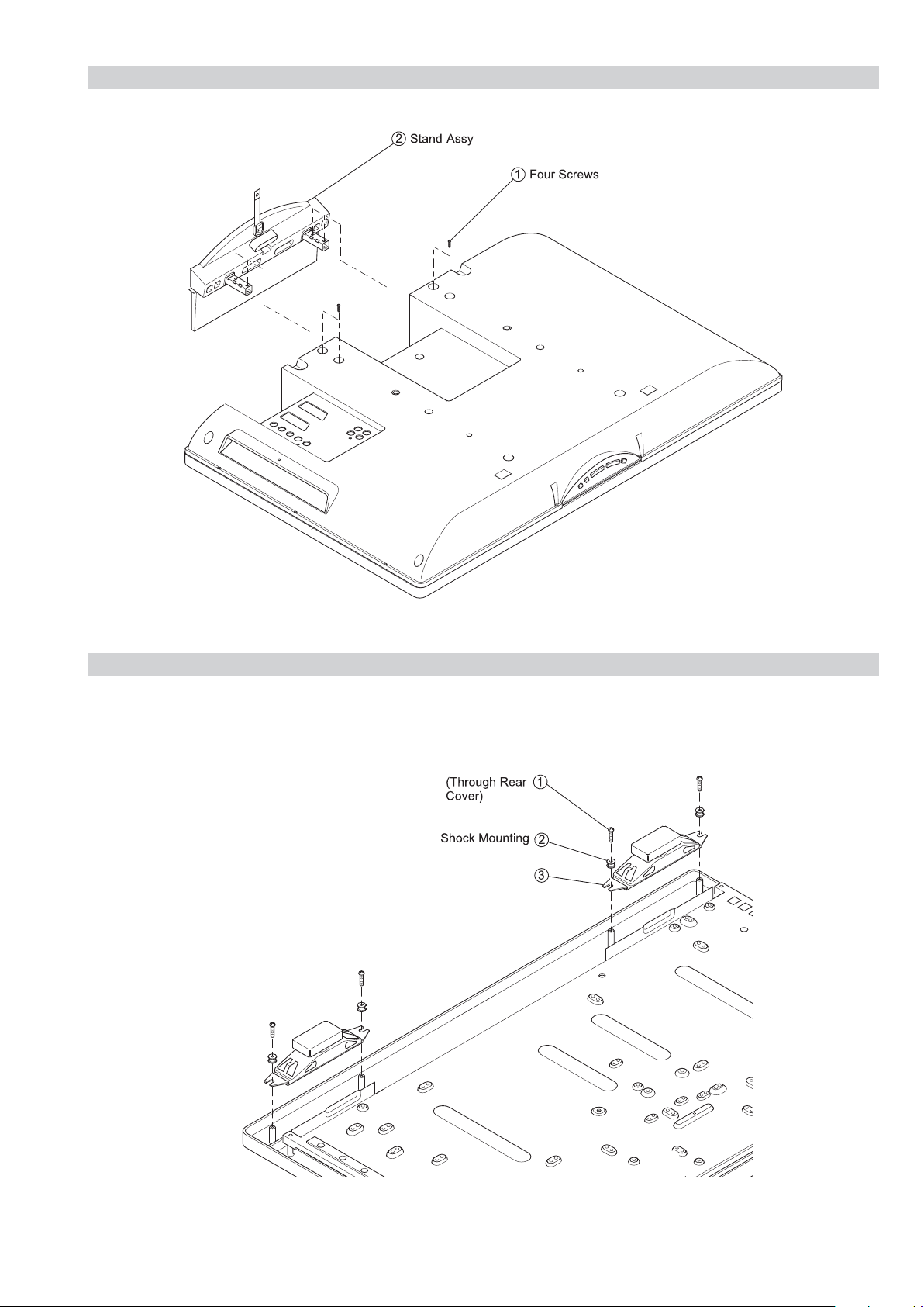
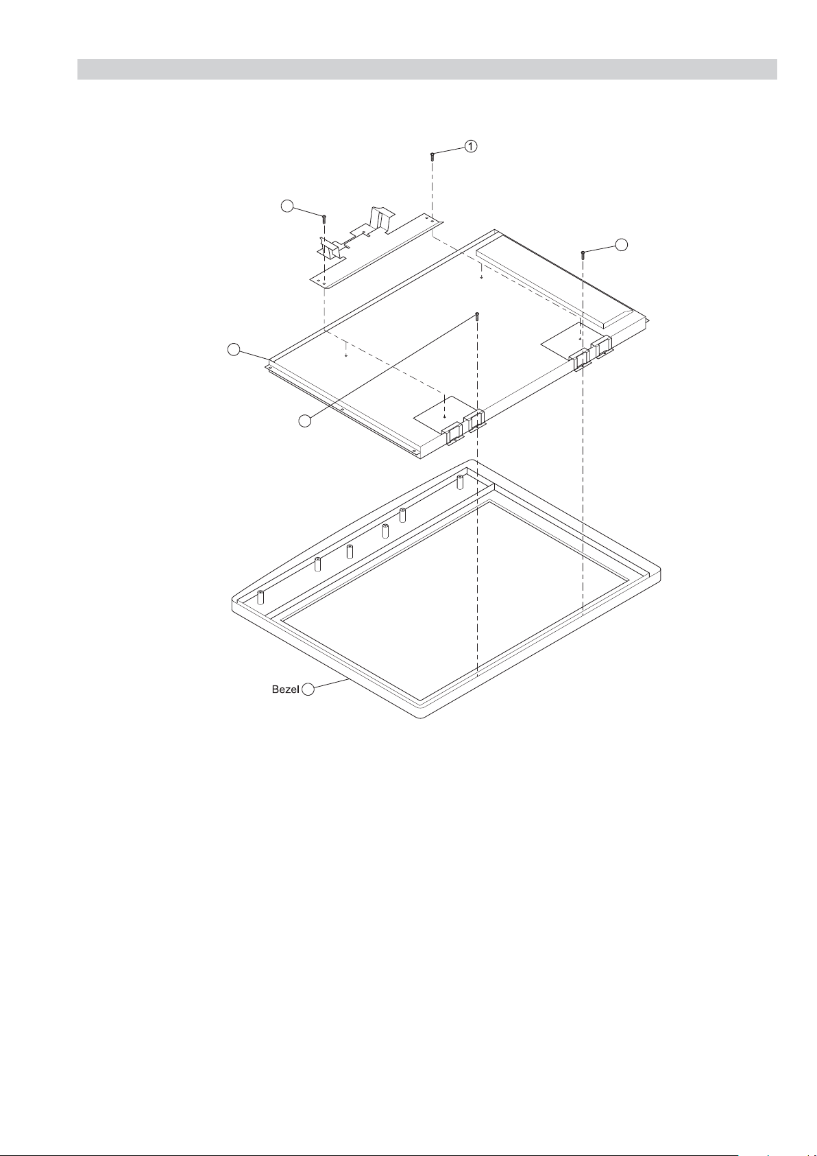
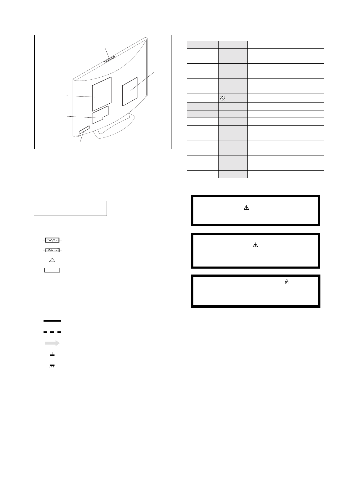
5-3. REAR COVER, STAND & BEZEL (26 & 32 Inches)
21
i
i
i
i
UK MODELS ONLY
i
i
i
i
i
j
o
o
k
l
m
o
m
n
i 2-580-644-01 SCREW, +KTP2 3X8
j 2-580-606-01 SCREW, +PSW M5X8
k 5-580-663-01 SCREW, WOOD 3.8X20
26
l 2-593-320-02 SCREW, COIN (M6X18)
m 2-580-640-01 SCREW, BVTP2 4X16
n 2-580-600-01 SCREW, +PSW M4X8
o 2-580-639-01 SCREW, +BVTP 4X12
REF.NO. PART.NO DESCRIPTION REMARK REF.NO. PART.NO DESCRIPTION REMARK
21 *X-2178-409-2 STAND (M) ASSY 26/32P3020
*X-2188-783-1 STAND (M_WS) ASSY 26/32P302H
26 X-2186-800-1 BEZEL (26P) ASSY 26 inches
X-2186-730-1 BEZEL (32P) ASSY 32 inches
- 3 -
5-4. REAR COVER, STAND & BEZEL (37 & 40 Inches)
31
p
p
p
p
UK MODELS ONLY
p
p
q
p
q
p
p
v
v
r
s
t
v
t
u
p 2-580-644-01 SCREW, +KTP2 3X8
q 2-580-607-01 SCREW, +PSW M5X12
r 5-580-663-01 SCREW, WOOD 3.8X20
36
s 2-593-320-02 SCREW, COIN (M6X18)
t 2-580-640-01 SCREW, BVTP2 4X16
u 2-580-600-01 SCREW, +PSW M4X8
v 2-580-639-01 SCREW, +BVTP 4X12
REF.NO. PART.NO DESCRIPTION REMARK REF.NO. PART.NO DESCRIPTION REMARK
31 *X-2187-520-2 STAND (ML) ASSY 37/40P3020
*X-2188-762-1 STAND (ML) ASSY 37/40P302H
36 X-2186-732-1 BEZEL (37P) ASSY 37 inches
X-2186-809-1 BEZEL (40P) ASSY 40 inches
- 4 -

9-927-578-02
Sony Corporation
Sony UK
Service Promotions Dept.
English
07KP7100-1
Printed in U.K.
© 2007.11

HISTORY
Model Name :
SERVICE MANUAL
Click on Page Number to display detail of changes.
Date Part Number Description of Revisions
Original Manual.
9-927-574-02 2007.11
Amendments to the exploded views (P74-77) and
addition of full size schematic diagrams (Full).
KDL-26/32/37/40P3000 & KDL-26/32/37/40P300H
Version
1.09-927-574-01 2007.10
2.0
SE2
RM-ED009
SERVICE MANUAL
MODEL
KDL-26P3000
KDL-32P3000
KDL-37P3000
KDL-40P3000
KDL-26P300H
KDL-32P300H
KDL-37P300H
KDL-40P300H
COMMANDER DEST
RM-ED009 AEP
RM-ED009 AEP
RM-ED009 AEP
RM-ED009 AEP
RM-ED009 AEP
RM-ED009 AEP
RM-ED009 AEP
RM-ED009 AEP
SE2
MODEL
KDL-26P3000
KDL-32P3000
KDL-37P3000
KDL-40P3000
KDL-26P300H
KDL-32P300H
KDL-37P300H
KDL-40P300H
COMMANDER DEST
CHASSIS
RM-ED009 UK
RM-ED009 UK
RM-ED009 UK
RM-ED009 UK
RM-ED009 UK
RM-ED009 UK
RM-ED009 UK
RM-ED009 UK
KDL-26P3000 / KDL-32P3000 / KDL-37P3000 / KDL-40P3000
KDL-26P300H / KDL-32P300H / KDL-37P300H / KDL-40P300H
FLAT PANEL COLOR TV
- 1 -
RM-ED009

SE2
RM-ED009
TABLE OF CONTENTS
Section Title Page Section Title Page
1. GENERAL ................................................................... 3
Caution ................................................................ 3
Specifications ...................................................... 5
Connectors .......................................................... 6
Self Diagnosis ..................................................... 8
2. DISASSEMBLY
2-1. Rear Cover Removal ........................................... 9
2-2. Stand Removal (26 & 32 inches) ........................ 9
2-3. Stand Removal (37 & 40 inches) ........................ 10
2-4. Loudspeaker Removal ........................................ 10
2-5. B1 Board Removal .............................................. 11
2-6. DS1 Board Removal (40 inches)........................ 11
2-7. GS2 Board Removal (26 & 32 inches)............... 12
2-8. GS3 (37 inches) or GS4 (40 inches)
Board Removal ................................................... 12
2-9. H1PS Board Removal ........................................ 13
2-10. H3PS Board Removal ........................................ 13
2-11. LCD Panel Removal ........................................... 14
3. CIRCUIT ADJUSTMENTS
3-1. Electrical Adjustments ....................................... 15
3-2. TT Mode ............................................................ 17
3-3. TT OSD Labels .................................................. 18
4. DIAGRAMS
4-1. Block Diagram .................................................... 19
4-2. Circuit Board Location ........................................ 20
4-3. Schematic Diagrams and Printed Wiring
Boards ................................................................. 20
B1 Board Schematic Diagram ............................. 21
DS1 Board Schematic Diagram (40 inches) ....... 46
GS2 Board Schematic Diagram
(26 & 32 inches) ................................................. 50
GS3 Board Schematic Diagram (37 inches) ....... 55
GS4 Board Schematic Diagram (40 inches) ....... 60
H1PS Board Schematic Diagram ....................... 65
H3PS Board Schematic Diagram ....................... 65
B1 Printed Wiring Board .................................... 66
H1PS Printed Wiring Board ............................... 66
H3PS Printed Wiring Board ............................... 67
DS1 Printed Wiring Board ................................. 68
GS2 Printed Wiring Board ................................. 69
GS3 Printed Wiring Board ................................. 70
GS4 Printed Wiring Board ................................. 72
5. EXPLODED VIEWS
5-1. Chassis (26 & 32 inches).................................... 74
5-2. Chassis (37 & 40 inches).................................... 75
5-3. Rear Cover, Stand & Bezel (26 & 32 inches) ..... 76
5-4. Rear Cover, Stand & Bezel (37 & 40 inches) ..... 77
6. ELECTRICAL PARTS LIST .................................. 78
WARNING !!
AN ISOLATION TRANSFORMER SHOULD BE USED DURING
ANY SERVICE WORK TO AVOID POSSIBLE SHOCK HAZARD
DUE TO LIVE CHASSIS, THE CHASSIS OF THIS RECEIVER IS
DIRECTLY CONNECTED TO THE POWER LINE.
SAFETY-RELATED COMPONENT WARNING !!
COMPONENTS IDENTIFIED BY SHADING AND MARKED
THE SCHEMATIC DIAGRAMS, EXPLODED VIEWS AND IN THE
PARTS LIST ARE CRITICAL FOR SAFE OPERATION. REPLACE
THESE COMPONENTS WITH SONY PARTS WHOSE PART
NUMBERS APPEAR AS SHOWN IN THIS MANUAL OR IN
SUPPLEMENTS PUBLISHED BY SONY.
ON
- 2 -
SECTION 1 GENERAL
SECTION 1 GENERAL
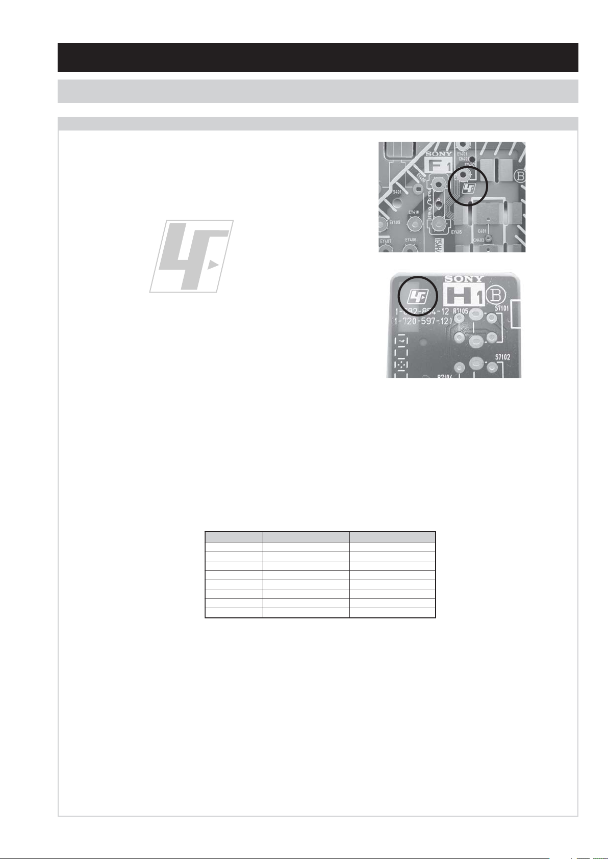
CAUTION
Lead Free Soldered Boards
The circuit boards used in these models have been processed using
Lead Free Solder. The boards are identified by the LF logo located
close to the board designation e.g. F1, H1 etc [ see examples ]. The
servicing of these boards requires special precautions to be taken as
outlined below.
SE2
RM-ED009
example 1
example 2
Lead Free Solder material must be used to comply with environmental requirements of new solder joints. Lead Free Solder is available under
the following part numbers :
rebmuntraP retemaiD skrameR
91-500-046-7mm3.0gK52.0
02-500-046-7mm4.0gK05.0
12-500-046-7mm5.0gK05.0
22-500-046-7mm6.0gK52.0
32-500-046-7mm8.0gK00.1
42-500-046-7mm0.1gK00.1
52-500-046-7mm2.1gK00.1
62-500-046-7mm6.1gK00.1
Due to the higher melting point of Lead Free Solder the soldering iron tip temperature needs to be set to 370 degrees centigrade. This requires
soldering equipment capable of accurate temperature control coupled with a good heat recovery characteristics.
For more information on the use of Lead Free Solder, please refer to http://www.sony-training.com
- 3 -
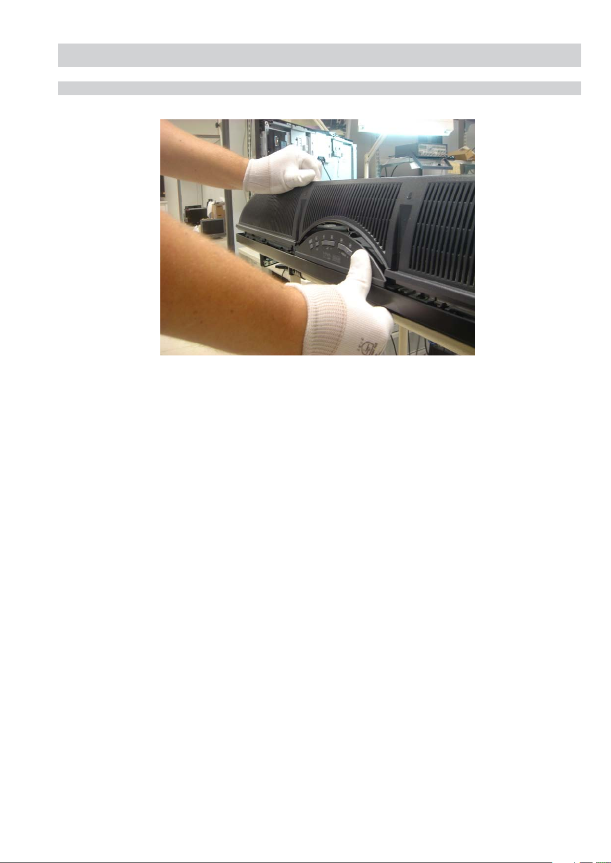
Rear Cover Removal
SE2
RM-ED009
CAUTION
When removing the rear cover it is important to ensure that the top button plate is fixed to the front cabinet and not removed with the rear cover.
This is to avoid breaking the cable connected to the switch button board. It is also important to remember that whilst removing the rear cover it
is kept parallel to the LCD plane.
- 4 -
SPECIFICATIONS
SE2
RM-ED009
ITEM MODEL Television System Stereo System Channel Coverage Color System
Analogue:
E
U
Projected Picture Size
Input/Output Terminals [REAR] General Specifications
1: 21-pin Euro connector
(CENELEC standard)
2: 21-pin Euro connector
(CENELEC standard)
Phono Jacks
HDMI Inputs HDMI Connectors
PC Input 15 Pin D Sub Connector
CAM Slot Conditional Access Module
Input/Output Terminals [SIDE] Remote control system : Infrared control
Headphone jack Stereo mini jack
Audio input Phono jacks
Video input Phono jack
S Video input 4 pin mini DIN
B/G/H, D/K, I, L
Digital:
DVB -T
Analogue:
I
Digital:
DVB -T
LCD(Liquid Crystal Display) Panel
Approx 26 inches (KDL-26XXXXX)
Approx 32 inches (KDL-32XXXXX)
Approx 37 inches (KDL-37XXXXX)
Approx 40 inches (KDL-40XXXXX)
Inputs for Audio and Video signals.
Inputs for RGB.
Outputs of TV Video and Audio
signals.
Inputs for Audio and Video signals.
Inputs for RGB.
Outputs of Video and Audio signals
(Selectable). SmartLink interface.
Output Connectors variable for
Audio Signals.
GERMAN/NICAM
Stereo
NICAM Stereo
Design and specifications are subject to change without notice.
Analogue: VHF : E2-E12
UHF : E21-E69
CATV : S1-S20
HYPER : S21-S41
D/K: R1-R12, R21-R69
L: F2-F10, B-Q, F21-F69
I: UHF B21-B69
Digital: VHF/UHF
Analogue: I: UHF B21-B69
Digital: VHF/UHF
Sound Output
Right and Left speaker
Sub-woofer
Power Requirements 220 - 240V
Power Consumption/
Standby
Dimensions
Weight
Supplied Accessories
Other Features
Power requirements
2 x 10W (RMS)
Approx 90W/0.7W or less (26 inches)
Approx 130W/0.7W or less (32 inches)
Approx 150W/0.6W or less (37 inches)
Approx 165W/0.6W or less (40 inches)
Approx 657x500x214mm
(26 inches with stand)
Approx 657x453x121mm
(26 inches without stand)
Approx 790x577x214mm
(32 inches with stand)
Approx 790x530x119mm
(32 inches without stand)
Approx 906x658x265mm
(37 inches with stand)
Approx 906x611x126mm
(37 inches without stand)
Approx 982x690x265mm
(40 inches with stand)
Approx 982x643x124mm
(40 inches without stand)
Approx 12.0kg (26 inches with stand)
Approx 10.0kg (26 inches without stand)
Approx 15.0kg (32 inches with stand)
Approx 13.0kg (32 inches without stand)
Approx 21.0kg (37 inches with stand)
Approx 18.0kg (37 inches without stand)
Approx 23.5kg (40 inches with stand)
Approx 20.0kg (40 inches without stand)
RM-ED009 Remote Commander (1)
IEC designated R06 battery (2)
Support belt (1) and screws (2)
Intergrated digital Tuner, High Picture Quality,
Bravia Engine, BBE ViVA, 2 HDMI inputs, PC
input.
3V dc
2 batteries IEC designation
R06 (size AA)
Analogue:
PA L , S E C A M
NTSC 3.58/4.43
(VIDEO ONLY)
Digital:
MPEG-2 MP@ML
Analogue:
PA L , S E C A M
NTSC 3.58/4.43
(VIDEO ONLY)
Digital:
MPEG-2 MP@ML
- 5 -
21 Pin Connector (SCART)
How to replace the fuse.
Open the fuse compartment with
a screwdriver blade and replace
the fuse.
FUSE
21
20
19
18
17
16
15
14
13
12
11
10
9
8
7
6
5
4
3
2
1
CONNECTORS
Pin No 1 2 Signal Signal level
1 Audio output B
2
3
4 Ground (audio)
5 Ground (blue)
6 Audio input A
7 Blue input 0.7 +/- 3dB, 75 ohms positive
8 Function select
9 Ground (green)
10 AVlink
11 Green Green signal : 0.7 +/- 3dB, 75 ohms,
12 Open
13 Ground (red)
14 Ground (blanking)
_ _ Red input 0.7 +/- 3dB, 75 ohms, positive
15
_ (S signal Chroma
-
16 Blanking input
17 Ground (video
18 Ground (video
19 Video output 1V +/- 3dB, 75ohms, positive sync 0.3V
Video input 1V +/- 3dB, 75ohms, positive sync 0.3V
20
--
21 Common ground
(right)
Audio input B
(right)
Audio output A
(left)
(left)
(AV control)
-
input)
(Ys signal)
output)
input)
Video input
Y (S signal)
(plug, shield)
RM-ED009
Standard level : 0.5V rms
Output impedence : Less than 1kohm*
Standard level : 0.5V rms
Output impedence : More than 10kohm*
Standard level : 0.5V rms
Output impedence : Less than 1kohm*
Standard level : 0.5V rms
Output impedence : More than 10kohm*
High state (9.5-12V) : Part mode
Low state (0-2V) : TV mode
Input impedence : More than 10K ohms
Input capacitance : Less than 2nF
positive
0.3 +/- 3dB, 75 ohms, positive
High state (1-3V) Low state (0-0.4V)
Input impedence : 75 ohms
(-3+10dB)
(-3+10dB)
1V +/- 3dB, 75ohms, positive sync 0.3V
(-3+10dB)
SE2
UK PLUG WARNING
WARNING (UK Models only)
The flexible mains lead is supplied connected to a B.S. 1363 fused
plug having a fuse of the correct rating for the set. Should the fuse
need to be replaced, use a fuse of the same rating approved by ASTA
to BS 1362, ie one that carries the
IF THE PLUG SUPPLIED WITH THIS APPLIANCE IS NOT SUITABLE FOR THE OUTLET SOCKETS IN YOUR HOME, IT SHOULD
BE CUT OFF AND AN APPROPRIATE PLUG FITTED. THE PLUG
SEVERED FROM THE MAINS LEAD MUST BE DESTROYED AS A
PLUG WITH BARED WIRES IS DANGEROUS IF ENGAGED IN A
LIVE SOCKET.
When an alternative type of plug is used, it should be fitted with the
correct rating fuse, otherwise the circuit should be protected by the
same rating fuse at the distribution board.
ASA
T
mark.
Connected Not Connected (open) * at 20Hz - 20kHz
- 6 -
HDMI Connector
1
SE2
RM-ED009
Pin No Signal Assignment Pin No Signal Assignment
1 TMDS Data2+ 11 TMDS Clock Shield
2 TMDS Data2 Shield 12 TMDS Clock-
3 TMDS Data2- 13 CEC
4 TMDS Data1+ 14 Reserved (N.C. on device)
5 TMDS Data1 Shield 15 SCL
6 TMDS Data1- 16 SDA
7 TMDS Data0+ 17 DDC/CEC Ground
8 TMDS Data0 Shield 18 +5V Power
9 TMDS Data0- 19 Hot Plug Detect
10 TMDS Clock+
15 Pin D Sub Connector (PC)
Pin No Signal Assignment Pin No Signal Assignment
1 Red Out 9 +5V DC
2 Green Out 10 Sync Return (Ground)
3 Blue Out 11 Monitor ID0 in Display
4 Unused 12 DCC Serial Data
5 Ground 13 Horizontal Sync
6 Red Return 14 Vertical Sync
7 Green Return (Ground) 15 DCC Serial Clock
8 Blue Return (Ground)
Rear Connection Panel Side Connection Panel
noitarugifnocniptekcosoediVS
S-Video
socket
niP
oN
1dnuorG-
2dnuorG-
3tupni)langisS(Y,mho57Bd3-/+V1
4tupni)langisS(CBd3-/+V3.0
langiS leveLlangiS
V3.0.cnySevitisop
Bd01+3-
ev
itisop,mho57
.cnyS
- 7 -
SE2
RM-ED009
SE2 SELF DIAGNOSTIC SOFTWARE
The identification of errors within the SE2 chassis is triggered in one of two ways :- 1: Busy or 2: Device failure to respond to IIC. In the event
of one of these situations arising the software will first try to release the bus if busy (Failure to do so will report with a continuous flashing
LED) and then communicate with each device in turn to establish if a device is faulty. If a device is found to be faulty the relevant device number
will be displayed through the LED (Series of flashes which must be counted).
LED Error Code
Number of LED
Flashes
02 Balancer error. In normal mode. Goes into standby.
03 Power supply protection error. In normal mode. Goes into standby.
04 Inverter error. In normal mode. Goes into standby.
05 NVM error. In initialisation state. Adds error to error menu.
06 IIC error. In normal mode. Adds error to error menu.
07 HDMI error. In initialisation state. Adds error to error menu.
08 Digital error. In normal mode. Adds error to error menu.
09 Tuner Error In initialisation state. Adds error to error menu.
10 Sound processor In initialisation state. Adds error to error menu.
13 Real time clock error In initialisation state. Adds error to error menu.
Error Description Checked Action
Error Descriptions
Error Description Meaning/Related Fault
Balancer error. Balancer error/PANEL_DET (PMUX2.0) to low level, between 2.48V and 0.83V.
Power supply protection error. 5V, 3.3V or 1.8V failure/POWER_DET (P3_6) to high level.
Panel error. Inverter failure/PANEL_DET (PMUX2.0) to low level, less than 0.83V.
NVM error. EEPROM cannot be read or written.
IIC error. IIC bus cannot be correctly initialised.
HDMI error. HDCP cannot be set-up correctly.
Digital error. Digital CPU does not respond by DPI communication (Only for digital models).
Tuner Error IF circuit or PLL circuit does not respond to IIC commands.
Sound processor MSP3410G IC does not respond to IIC commands.
Real time clock error RTC IC does not respond to IIC commands (Only for digital models).
- 8 -
2-1. REAR COVER REMOVAL
6
SE2
RM-ED009
SECTION 2 DISASSEMBLY
7
2-2. STAND REMOVAL (26 & 32 inches)
Three Screws
– 9 –
2-3. STAND REMOVAL (37 & 40 inches)
SE2
RM-ED009
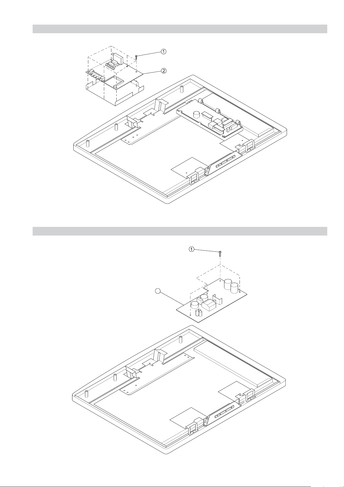
2-4. LOUDSPEAKER REMOVAL
Two Screws
Loudspeaker
– 10 –
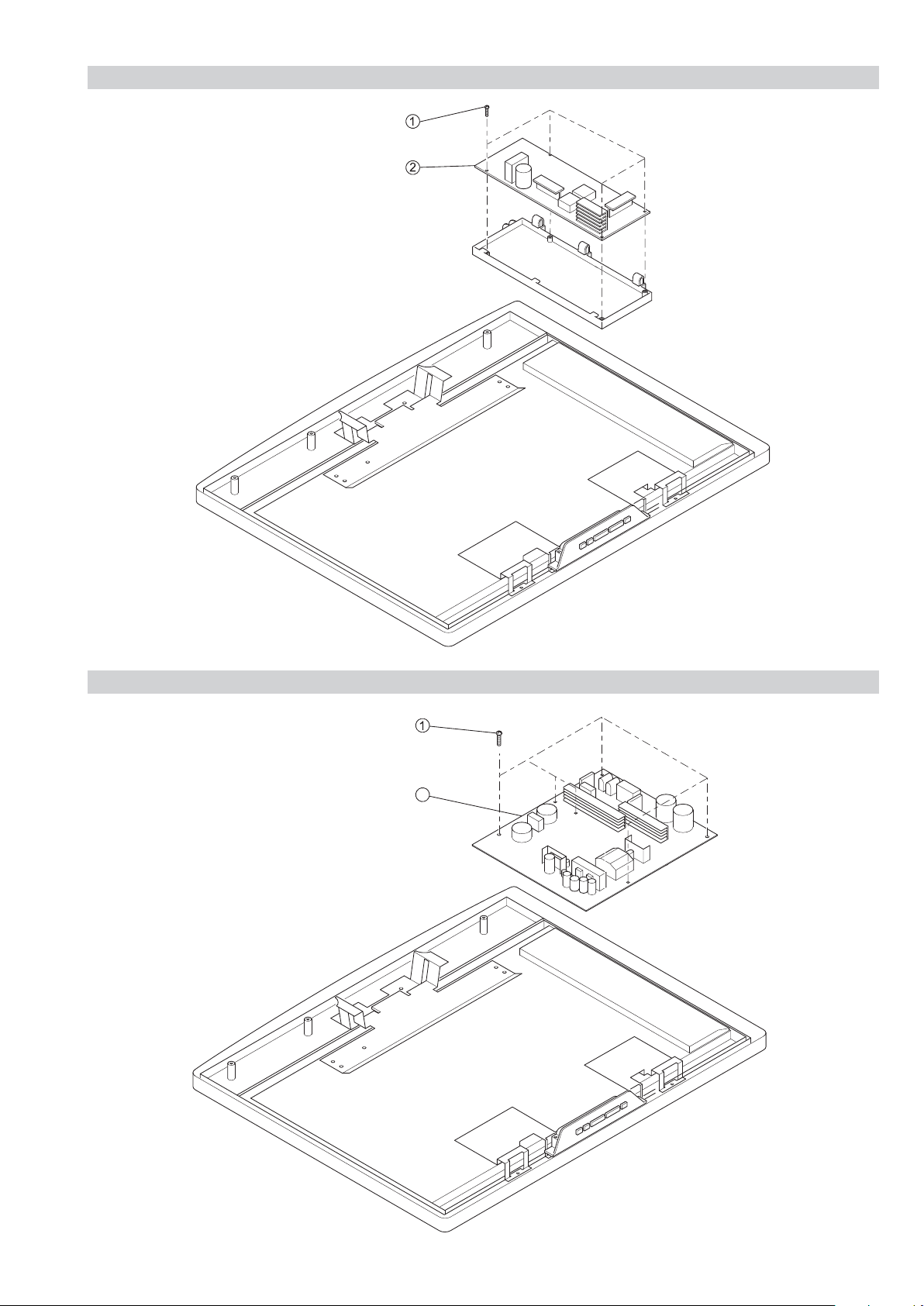
2-5. B1 BOARD REMOVAL
SE2
RM-ED009
Six Screws
B1 Board
2-6. DS1 BOARD REMOVAL (40 inches)
DS1 Board
Four Screws
2
– 11 –
2-7. GS2 BOARD REMOVAL (26 & 32 inches)
Four Screws
GS2 Board
SE2
RM-ED009
2-8. GS3/GS4 BOARD REMOVAL (37/40 inches)
Six Screws
GS3/GS4 Board
2
– 12 –
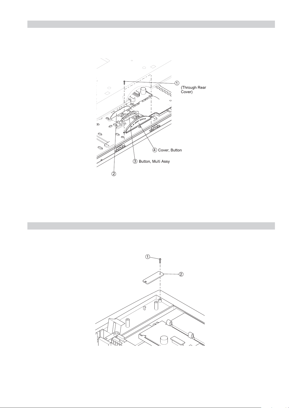
2-9. H1PS BOARD REMOVAL
SE2
RM-ED009
Two Screws
2-10. H3PS BOARD REMOVAL
H1PS Board
One Screw
H3PS Board
– 13 –
2-11. LCD PANEL REMOVAL
SE2
RM-ED009
Two Screws
LCD Panel
Two Screws
5
One Screw
2
3
One Screw
4
6
– 14 –
SECTION 3 CIRCUIT ADJUSTMENTS
3-1. Electrical Adjustments
Service adjustments to this model can be performed using the
supplied remote commander RM-ED009.
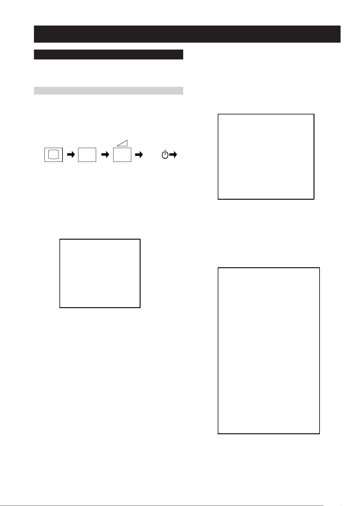
How to enter into the Service Mode
1. Turn on the power to the TV set and enter into the stand-by
mode.
2. Press the following sequence of buttons on the remote
commander.
+
i+
(ON SCREEN (DIGIT 5) (VOLUME +) (TV)
DISPLAY)
5
‘TT—’ will appear in the upper right corner of the screen.
Other status information will also be displayed (See 3-3 page
18).
+
TV
I/
BACKLIGHT
BACKLIGHT
U BACKLIGHT
BL SETUDEN
BL BOTTOM
ECO MODE
APL MAX
DIMMER MIN
APL FACTOR
OSD CONTR MIN
DIMMER
APL MIN
(0, 255)
(0, 10)
(0, 255)
(0, 255)
(0, 1)
(0, 255)
(-128, +127)
(0, 255)
(0, 255)
(0, 255)
(0, 255)
SE2
RM-ED009
235
10
38
92
1
140
-32
0
40
186
103
3. Press ‘MENU’ on the remote commander to obtain the
following menu on the screen.
BACKLIGHT
HDMI
SOUND
IF ADJUST
PANEL T E M P
ERROR MENU
SE2 v0.10
FACTORY DATA: 11111111
SERIAL NUMBER: 4294967295
WORKING TIME: 0:22
4. Move to the corresponding adjustment item using the
up or down arrow buttons on the Remote Commander.
5. Press the right arrow button to enter into the required menu
item.
6. Press the ‘Menu’ button on the Remote Commander to quit
the Service Mode when all adjustments have been completed.
Note :
• After carrying out the service adjustments, to prevent the
customer accessing the ‘Service Menu’ switch the TV set
OFF and then ON again.
HDMI
VAI2
VAI3
Vper MSB
Vper ISB
Hper MSB
HS Width MSB
STM LSB
Ri (MSB)
Ri (LSB)
Aksv_0
Aksv_1
Aksv_2
Aksv_3
Aksv_4
An_0
An_1
An_2
An_3
An_4
An_5
An_6
An_7
Pj
Ainfo
Flags
(0, 255)
(0, 255)
(0, 255)
(0, 255)
(0, 255)
(0, 255)
(0, 255)
(0, 255)
(0, 255)
(0, 255)
(0, 255)
(0, 255)
(0, 255)
(0, 255)
(0, 255)
(0, 255)
(0, 255)
(0, 255)
(0, 255)
(0, 255)
(0, 255)
(0, 255)
(0, 255)
(0, 255)
(0, 255)
0
0
3
31
0
0
176
218
101
0
0
0
0
0
0
0
0
0
0
0
0
0
202
0
6
- 15 -

SE2
RM-ED009
SOUND
Lineout offset
M-N
M-D
M-S
S-M
D-M
N-M
Effect Mode
BBE Mode
BBE Vol main
BBE Vol res
B1
B2
B3
B4
B5
Loudness
MB_STR
MB_LIM
MB_HMC
MB_LP
MB_HP
SUBW_FREQ
NICAM C AD
NICAM Error
Stereo
Status 0000000110
(-80, +40)
(0, 511)
(-128, -1)
(+0, +127)
(+0, +127)
(-128, -1)
(0, 1023)
(+0, +2)
(-0, +127)
(+0, +255)
(+0, +7)
(-96, +96)
(-96, +96)
(-96, +96)
(-96, +96)
(-96, +96)
(+0, +68)
(+0, -127)
(-32, +0)
(+0, +127)
(+5, +30)
(+3, +30)
(+5, +40)
(0, 2047)
(-128, +127)
00000
+8
192
-20
+20
+10
-10
496
+1
+0
+3
+0
+8
+2
-12
-12
+6
+23
+0
+0
+0
+5
+3
+5
2047
+0
PANE L TEM P
TEMPERATURE (0, 125) 33
ERROR MENU
IF ADJUST
Automute
Audio Gain
L Gating
Coincidence
AFT window
AFT Status
AGC TOP (-16, +15)
0111
E02: BALANCER
E03: DC Fail
E04: INVERTER
E05: NVM
E06: IIC
E07: HDMI
E08: DIGITAL
E09: TUNER
E10: SP
E13: RTC
WORKING TIME
0
0
0
0
1
+0
HOURS
MINUTES
(0, 255)
(0, 255)
(0, 255)
(0, 255)
(0, 255)
(0, 255)
(0, 255)
(0, 255)
(0, 255)
(0, 255)
(0, 65535)
(0, 59)
0
0
0
0
0
0
0
0
0
0
0
0
- 16 -
RM-ED009
3-2. TT MODE
TT mode is available by setting the TV for operation in Service Mode [ As shown on Page 15 ] , OSD ‘TT’ appears. The functions described
below are available by selecting the two numbers. To release the ‘Test mode 2’, press 00, 10, 20 ... twice or switch the TV set into Stand-by
mode. In ‘TT Menu’ mode, it is possible to remove the Menu from the screen by pressing the Speaker Off button once. Pressing the Speaker
OFF button a second time will cause the Menu to reappear. The function is kept even when the menu is not displayed on screen !!.
SE2
'TT' mode off
00
Set volume to 35%
03
Set volume to 50%
04
Set volume to 65%
05
Set volume to 80%
06
Ageing mode on
07
Shipping Condition
08
WB adj initial conditions
09
Teletext centered
14
Factory toggle mode (on/off)
19
CBA mode toggle (ON/OFF)
27
ECS mode toggle (ON/OFF)
31
Set BCN channels preset
32
Connect/Disconnect EDID write o general I2C bus
33
HDMI log enable/disable
34
35 Hotel mode toggle
PC Monitor mode toggle
37
38 OTRUM mode
Enable Digital Test
39
41 Re-initialise NVM
Select Dual Sound "A"
43
Select Dual Sound "B"
44
Select Dual Sound "Mono"
45
Select Dual Sound "Stereo"
46
Set NVM as non-virgin
48
Set NVM as virgin
49
Hybrid/ALPS tuner selection
51
Temperature sensor enable/disable
52
Digital/Analog model
53
Watchdog toggle
54
Audio delay toggle
55
Set Bravia Model enable/disable
56
MSP Auto Carrier Mute function enable/disable
57
Chip select toggle
58
Visual I2C toggle
59
Set 15" 4:3 XGA settings
61
Set 20" 4:3 VGA settings
62
Set 20" WXGA settings
63
Set 23" WXGA settings
64
Set 26" WXGA settings
65
Set 32" WXGA settings
66
Set 37" WXGA settings
67
Set 40" WXGA settings
68
71 Auto AGC
AM from baseband (AFRIC dem) or fromRF (MSP
72
dem)
73 HDMI number of inputs (0 to 2)
DDC enable
74
Set centred balance
75
76 Set volume to max
Set volume to min
77
Set balance full left
78
Set balance full right
79
Digital BER display
81
Digital Service menu
82
Digital colour bar output from DENC
83
TS CI path through
84
Digital tuner power down (Only 1 power cycle,default
85
is no power down)
Switch between two digital SW banks
86
87 Local keys test
Digital shipping conditions (Clear tune database)
88
89 LED test
OAD enable/disable toggle
91
TS CI path through with Reed Solomon off
92
Spread spectrum toggle
94
Digital debug output enable/disable
96
Digital 656 output enable/disable
97
Digital auto reset function enable/disable
98
Display error and working time menu
99
- 17 -

3-3. TT OSD Labels
SE2
RM-ED009
(1)
26
ECS
DDC
(13)
-
Key:
1. Panel size configuration. Changed by TT61...TT68.
2. D/A: D is shown when Digital mode is enabled; A is shown when Analogue mode is enabled. Changed by TT53.
3. TT-- command prompt.
4. ECS/---: ECS enabled/disabled (TT31).
5. CBA/--: CBA is shown when the TV set is in CBA mode (This mode is available from Factory mode TT19). Changed by TT27.
6. Norm/Fact: Normal or Factory mode. Changed by TT19.
7. DDC/---: DDC enabled/disabled. Changed by TT74.
8. 0/1/2: 0 or 2 HDMI inputs toggle. Changed by TT73.
9. E/-: E is shown when EDID WP is enabled; - is shown otherwise. Changed by TT33.
10. M/HO/-: M is shown when PC monitor mode is enabled changed by TT37; H is shown when Hotel mode is enabled changed by TT35;
O is shown when OTRUM is enabled changed by TT38; - is shown otherwise.
11. C/-: C (Default value) is shown when MSP Auto Carrier Mute function is enabled; - is shown otherwise. Changed by TT57.
12. M/A: M (Default value) is shown when AM sound is demodulated in MSP; A is shown when AFRIC demodulator is used. Changed by
TT72.
13. N/A: Previously used to indicate Clk enabled.
14. T/-: T is shown when digital test is enabled; - is shown otherwise. Changed by TT39.
15. W/-: W is shown when watchdog is enabled; - is shown otherwise. Changed by TT54.
16. C/-: C is shown when chip select is enabled; - is shown instead. This mode is only available in factory mode. Changed by TT58.
17. V/-: V is shown when visual I2C is enabled; - is shown otherwise. Changed by TT59.
18. D/-: D is shown when audio delay is enabled; - is shown otherwise. Changed by TT55.
19. K/-: K is shown when spread spectrum is enabled; - is shown otherwise. Changed by TT94.
20. B/-: B is shown for BRAVIA models; -is shown otherwise. This mode is only available in factory mode. Changed by TT56.
21. S/-: S is shown if temperature sensor is enabled; - is shown otherwise. Changed by TT52.
22. L/-: L is shown when HDMI is enabled; - is shown otherwise. Changed by TT34.
23. X/-: X is shown when teletext is centered (Default value); - is shown otherwise. Changed by TT14.
24. H/A: H is shown when Hybrid tuner is selected; A is shown if ALPS tuner is selected. Changed by TT51.
(4)
CBA
(7)
2
T
(8)
(14)
E
W
"
(5)
(9)
(15)
D
B
S
C
(2)
(20)
(21)
(16)
H
V
(10)
(17)
C
D
(11)
(18)
TT - No r m
(12)
M
K
(19)
L
X
(22)
(23)
H
(3)
(6)
(24)
- 18 -
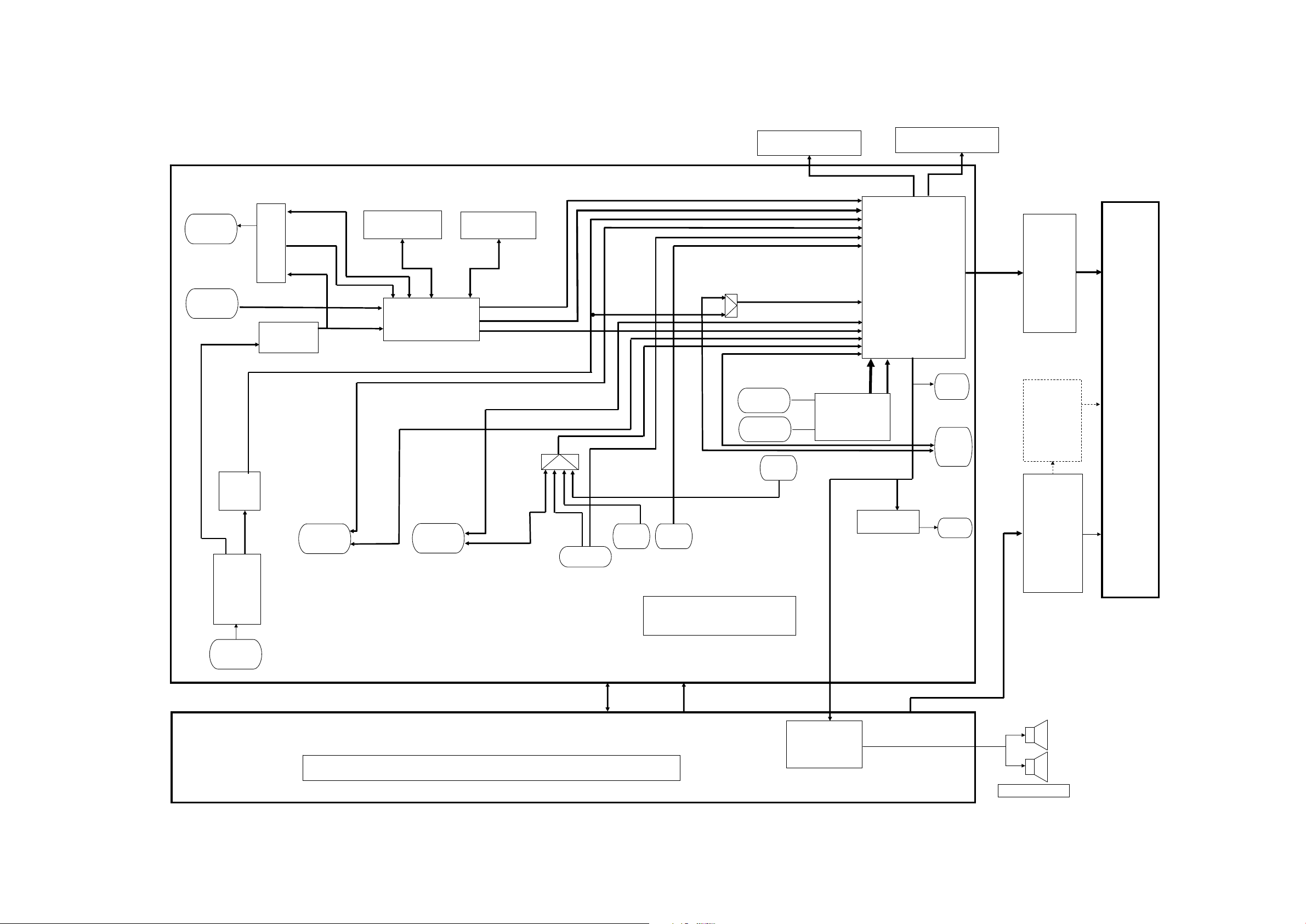
4-1. BLOCK DIAGRAM
SE2
RM-ED009
PCMCIA
JIG MS
IF IC
B
U
F
F
E
R
S
COFDM
Decoder
NAND
VIDEO PROCESSOR
DDR
HDMI1
HDMI2
H3PS
AUDIO
HDMI
SIRCS, LED
HDMI decoder
H1PS
SWITCH-BUTTONS
VIDEO PROCESSOR
AUDIO
OUT
Video
Audio
side in
T-CON
DS1
BALANCER
(only for 40"
panel)
P
A
N
N
E
L
TUNER
RF
SCART1
SCART2
COMP
AUDIO
GS2, GS3, GS4 POWER SUPPLY BOARD
PC
PC
B1
SIGNAL BOARD
SPEAKERS
AMPLIFIER
HP AMPLIFIER
HP
INVERTER
SPEAKERS
- 19 -
4-2. CIRCUIT BOARD LOCATION
5-2. CIRCUIT BOARD LOCATION
SE2
RM-ED009
Reference Information
H1PS
C
C
N
VM
CVM Board
H
GS2/GS3/GS4
D1
4-3. SCHEMATIC DIAGRAMS AND
5-3. SCHEMATIC DIAGRAMS AND
PRINTED WIRING BOARDS
PRINTED WIRING BOARDS
Note :
• All capacitors are in µF unless otherwise noted.
• pF : µµF 50WV or less are not indicated except for
electrolytic types.
• Indication of resistance, which does not have one for
rating electrical power, is as follows.
Pitch : 5mm
Electrical power rating : 1/4W
• Chip resistors are 1/10W
• All resistors are in ohms.
k = 1000 ohms, M = 1000,000 ohms
• : nonflammable resistor.
• : fusible resistor.
• : internal component.
• : panel designation or adjustment for repair.
• All variable and adjustable resistors have
characteristic curve B, unless otherwise noted.
• All voltages are in Volts.
• Readings are taken with a 10Mohm digital mutimeter.
• Readings are taken with a color bar input signal.
• Voltage variations may be noted due to normal production
tolerences.
•: B + bus.
A
DS1
A Board
H3PS
D
D2
S1 Board
A
B1
J
A1
A2
RESISTOR RN
RC
FPRD
FUSE
RS
RB
RW
COIL LF-8L
CAPACITOR TA
PS
PP
PT
MPS
MPP
ALB
ALT
ALR
Note :
The components identified by shading
and marked are critical for safety.
Replace only with the part numbers
specified in the parts list.
Note :
Les composants identifiés par une trame et
par une marque sont d'une importance
critique pour la sécurité. Ne les remplacer
que par des pièces de numéro spécifié.
specified.
Note :
The components identified by mark
confidential information.
Strictly follow the instructions whenever the
components are repaired and/or replaced.
: METAL FILM
: SOLID
: NON FLAMMABLE CARBON
: NON FLAMMABLE FUSIBLE
: NON FLAMMABLE METAL OXIDE
: NON FLAMMABLE CEMENT
: NON FLAMMABLE WIREWOUND
: ADJUSTMENT RESISTOR
: MICRO INDUCTOR
: TANTALUM
: STYROL
: POLYPROPYLENE
: MYLAR
: METALIZED POLYESTER
: METALIZED POLYPROPYLENE
: BIPOLAR
: HIGH TEMPERATURE
: HIGH RIPPLE
contain
• : B - bus.
• : RF signal path.
• : earth - ground.
• : earth - chassis.
Note: Schematic diagrams are for reference only. Please refer to the electrical parts list for
the correct value and part number of components.
- 20 -
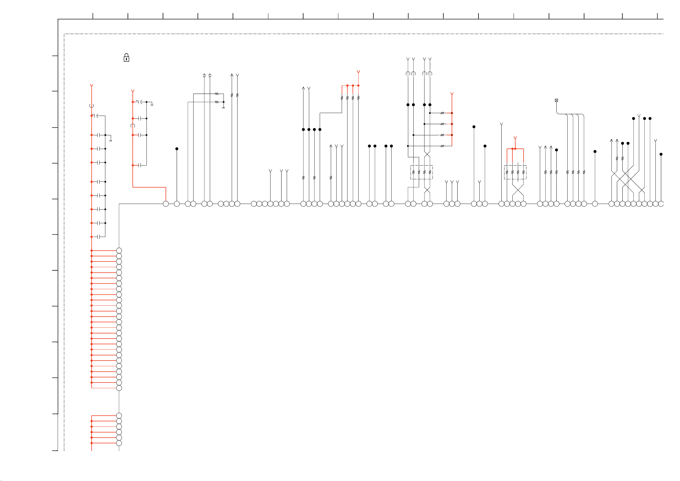
10
1
11
1
2
4
5
6
8
9
3
7
ABCD EF GH JIKLMN
O
B1.SE2
SCL_DIGITAL
SDA_DIGITAL
SDA_EMMA
B1
FE_+1V5
3.3V_MAIN
C7100
0uH
XX
FB7100
C7101
4.7
GND_1
C7104
0.1
C7105
0.1
C7106
0.1
C7107
0.1
C7108
0.1
C7109
0.1
C7110
THESE CAPACITORS TO BE PLACED UNDERNEATH BGA
0.1
0uH
FB7102
U16
VDD1
U15
VDD1
U14
VDD1
U10
VDD1
U9
VDD1
U8
VDD1
U7
VDD1
T5
VDD1
R5
VDD1
P17
VDD1
P5
VDD1
N5
VDD1
M5
VDD1
L17
VDD1
L5
VDD1
K17
VDD1
K5
VDD1
J17
VDD1
J5
VDD1
H17
VDD1
H5
VDD1
E16
VDD1
E15
VDD1
E14
VDD1
E7
VDD1
E6
VDD1
C7117
XX
GND_1
C7119
XX
C7120
XX
C7121
XX
THIS CAPACITOR TO BE
1A/13
JL7100
SIGN15015
PLACED UNDERNEATH BGA
R17
P21
R20
P21
R17
VDD3_USB
USBCLKI / PPORT105
SIGN15007
R21
R20
R21
USB_DP1
USB_DN1
FE_USB_DN
FE_USB_DP
R7100
10k
R7101
10k
T20
T21
T20
T21
USB_DP0
USB_DN0
FE_USB_PON
FE_NUSB_OVR
XX
XX
R7103
R7102
GND_1
U18
U19
U20
U21
AA3
Y4
U18
U19
U20
U21
USB_OCI1 / PPORT108
USB_OCI0 / PPORT106
USB_PPON1 / PPORT109
USB_PPON0 / PPORT107
Y4
AA3
MSDATA3 / PPORT127
FE_MS_BS
FE_MS_CLK
FE_MS_DAT[0]
W4
W3
V5
Y3
AA2
V5
Y3
W4
W3
AA2
MSBS / PPORT130
MSDIR / PPORT128
MSDATA2 / PPORT126
MSDATA1 / PPORT132
MSCLK / PPORT129
MSDIO/DATA0 / PPORT131
FE_TXD0B
FE_RXD0B
R7107 47
R7108 47
R7110 47
R7109 47
JL7105
JL7102
JL7103
JL7104
FE_TXD1B
FE_RXD1B
FE_M_SYNC
SIGN14963
SIGN14971
R7104100
R7105XX
R7106100
Y15
V15
AA1
W15
AA5
AA6
B5
C5
M19
L20
B5
C5
V15
Y15
AA1
W15
AA5
AA6
TXD1B
RXD1B
L20
M19
DCD1B / PPORT55
CTS0B / CAP/COMP1 / PPORT111
RTS0B / CAP/COMP2 / PPORT112
TXD0B / CAP/COMP0 / PPORT110
RXD0B / CAP/COMP3 / PPORT137
RTS1B_B / STP0_STRT / PPORT10
CTS1B_B / STP0_ERRB / PPORT11
3.3V_MAIN
CI2_RSTB
CI2_VS1B
CI2_IREQB
TP7100
TP7101
W19
AA19
N18
N18
W19
AA19
RI1B / PPORT54
TXD2B / PPORT14
RXD2B / PPORT13
VDO_VHSB /
VDO_VVSB /
nCI2_TSEN
TP7103
TP7102
L21
L21
TXD3B / PPORT53
RXD3B / PPORT52
SCL_EMMA
FB7105 0uH
FB7104 0uH
TP7104
TP7105
100
RB7100
Y8
AA8
Y8
AA8
SDA1
FB7106 0uH
TP7106
2143658
Y7
Y7
SCL1
SDA0
0uH
FB7107
TP7107
7
AA7
AA7
SCL0
3.3V_MAIN
R7111
4.7k
R7112
4.7k
R7113
XX
R7114
XX
FE_FTV_CONFIG2
FE_FTV_CONFIG0
FE_FTV_CONFIG1
P19
R18
N20
P19
R18
N20
SDIN / PPORT44
SDOUT / PPORT45
SCKINOUT / PPORT46
TP7112
CI2_CD1B
SIGN14979
SIGN14994
FE_MS_INS
V18
P18
W18
P18
V18
W18
IR_IN_1 / PPORT47
IR_IN_0 / PPORT51
TV_DEM_SEL
TP7115
RB7101 10 k
T19
T19
IR_OUT / PPORT48
SMRST0 / PPORT39
FE_ABCK,FE_ADO,FE_ALRCK,FE_AMCK
3.3V_MAIN
FE_NCI1_OVR
FE_NCI_EN
FE_CI1_PWR_EN
JL7106
R7115 47
R7116 47
V9
T18
N21
P20
R19
P20
T18
R19
N21
OFF0 / DCD0B / PPORT41
CMDVCC0 / RI0B / PPORT40
SMCLK0 / DTR0B / PPORT42
SMDAT0 / DSR0B / PPORT43
W7
Y6
V9W7Y6
AO1_DAT / PPORT125
AO1_BCK / PPORT124
AO1_LRCK / PPORT123
FE_ADO
FE_ALRCK
R7118 47
R7117 XX
R7119 47
V8
W6
Y5
V8
Y5
W6
AO0_DAT
AO0_LRCK
AO1_MCK / PPORT122
FE_ABCK
FE_AMCK
R7122 47
R7120 47
AA4
W5
W5
AA4
AO0_BCK
AO0_MCK
P
JL7107
SIGN14984
V6
V6
ATX
JL7109
FE_NDEMOD_RESET
FE_USB_PON
TP7119
JL7108
FE_NDEMOD_RESET
47
47
R7127
R7126
D20
F19
F18
E21
E19
F19
F18
E21
D20
E19
PAR / PPORT56
IRDYB / PPORT58
TRDYB / PPORT59
FRAMEB / PPORT57
IC7100
Q
DIG_OSD_STATUS
TP7120
JL7110
FE_JIG_MODE
JL71
H21
E20
M18
N19
E18
E20
H21
IDSEL / PPORT61
STOPB / PPORT60
E18
N19
M18
REQB0 / PPORT63
PERRB / PPORT65
GNTB0 / PPORT64
DEVSELB / PPORT62
12
E13
VDD2
E12
VDD2
E11
VDD2
E10
VDD2
E9
VDD2
E8
E8 E9 E10 E11 E12 E13 E6 E7 E14 E15 E16 H5 H17 J5 J17 K5 K17 L5 L17 M5 N5 P 5 P17 R5 T5 U7 U8 U9 U10 U14 U15 U16
VDD2
~ B1 Board Schematic Diagram [ Main Microcontroller, HDMI/AV Side/PC Input, Audio Processor, Scarts ] Page 1A/13 ~
- 21 -
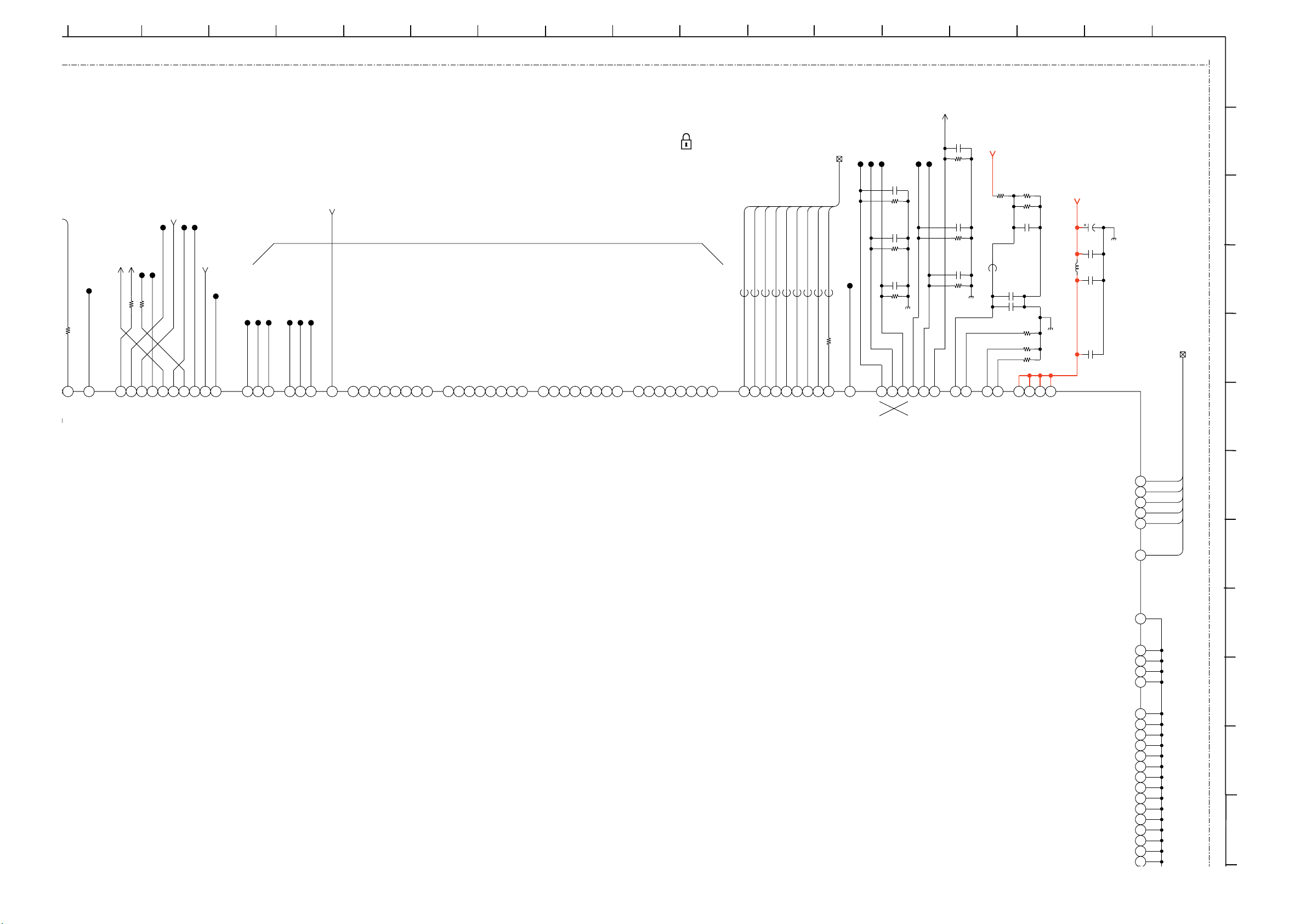
R7122 47
FE
AMCK
_
JL7107
SIGN14984
W5
W5
AO0_MCK
QRST UVWXY AA
Z
DDCCBBP
EE
FF
1
FE_CVBS
NOTE SYMBOL
IS WRONG
Y12
VAC
Y12
C7132
R7141
200
C7133
R7142
200
C7134
R7143
200
GND_1
W13
W13
VACVBS
10p
XX
XX
Y11
Y11
VREF1
VREF0
FE_+1V5
NOTE RESISTORS R7153..R7158 ARE 0.5% TOLERANCE
R7145
0uH
FB7117
Y13
Y13
R7144
330
W11
W11
RSET1
RSET0
0.1
C7136
0.1
C7137
680
C7135
R7147
R7148
470
R7149
XX
V14
V14
AVDDV
XX
R7146
4.7
THESE CAPACITORS
TO BE PLACED
UNDERNEATH BGA
0
GND_1
W14
Y14
Y14
W14
AVDDV
AVDDV
AA14
AA14
AVDDV
10uH
L7100
3.3V_MAIN
C7142
10
C7143
0.1
C7144
0.1
C7145
0.1
NMI/EDINT
GND_1
THIS CAPACITOR TO BE
PLACED UNDERNEATH BGA
FE_JTCK
JTCK
JTDI
JTDO
JTMS
JTRST
AA9
FE_JTDI
W8
FE_JTDO
W9
FE_JTMS
Y9
FE_JTRST
AA10
FE_NMI_EDINT
V10
2
3
4
FE_JTCK,FE_JTDI,FE_JTDO,FE_JTMS,FE_JTRST,FE_NMI_EDINT
5
6
7
8
B1
FE_NUSB_OVR
DIG_OSD_STATUS
TP7120
JL7110
JL7109
RESERVED FOR HI_RES GRAPHICS
FE_NDEMOD_RESET
FE_USB_PON
TP7119
JL7108
FE_NDEMOD_RESET
47
47
R7127
R7126
V6
D20
F19
F18
E21
E19
V6
F19
D20
H21
F18
E21
E19
H21
E20
E20
FE_JIG_MODE
JL7111
M18
N19
N19
M18
TP7121
TP7122
E18
B17
C17
E18
D17
B17
C17
D17
TP7125
A19
D21
M20
K21
A17
C18
B21
A21
C18
D21
K21
M20
B21
A17
A21
B18
B20
A20
A18
G20
G19
G18
F21
D18
C21
C20
C19
K18
J21
J20
J19
H20
H19
H18
G21
J18
F20
D19
B19
L19
L18
J21
J20
B20
B18
A20
A19
A18
F21
C21
C20
G20
G19
G18
C19
D18
J19
K18
H19
H20
J18
H18
F20
G21
D19
K20
L19
L18
B19
K20
TP7126
TP7124
TP7123
1B/13
VDO[7]
VDO[6]
VDO[5]
VDO[4]
VDO[3]
VDO[2]
VDO[1]
0uH
0uH
0uH
0uH
FB7108
FB7109
K19
V21
K19
V21
V20
V20
FB7111
FB7110
W21
W20
W21
W20
0uH
0uH
FB7112
FB7113
Y21
Y20
Y21
Y20
0uH
FB7114
AA21
AA21
ATX
PAR / PPORT56
FRAMEB / PPORT57
IDSEL / PPORT61
IRDYB / PPORT58
STOPB / PPORT60
TRDYB / PPORT59
REQB0 / PPORT63
DEVSELB / PPORT62
PERRB / PPORT65
GNTB0 / PPORT64
VDOE_VCK_IN / AD1 / PPORT70
VDOE_VVSB_IN / AD2 / PPORT71
VDOE_A5 / AD9 / PPORT78
VDOE_A7 / AD11 / PPORT80
VDOE_A6 / AD10 / PPORT79
VDOE_FLD / AD0 / PPORT69
VDOE_VCK / SERRB / PPORT66
VDOE_VHSB_IN / AD3 / PPORT72
VDOE_VVSB_OUT / INTAB / PPORT67
VDOE_VHSB_OUT / PCICLK / PPORT68
VDOE_A4 / AD8 / PPORT77
VDOE_A3 / AD7 / PPORT76
VDOE_A2 / AD6 / PPORT75
VDOE_A1 / AD5 / PPORT74
VDOE_A0 / AD4 / PPORT73
VDOE_R7 / AD19 / PPORT88
VDOE_R6 / AD18 / PPORT87
VDOE_R5 / AD17 / PPORT86
VDOE_R4 / AD16 / PPORT85
VDOE_R3 / AD15 / PPORT84
VDOE_R2 / AD14 / PPORT83
VDOE_R1 / AD13 / PPORT82
VDOE_R0 / AD12 / PPORT81
VDOE_G7 / AD27 / PPORT96
VDOE_G6 / AD26 / PPORT95
VDOE_G5 / AD25 / PPORT94
VDOE_G4 / AD24 / PPORT93
VDOE_G3 / AD23 / PPORT92
VDOE_G2 / AD22 / PPORT91
VDOE_G1 / AD21 / PPORT90
VDOE_G0 / AD20 / PPORT89
VDOE_B7 / CBE3 / PPORT104
VDOE_B3 / AD31 / PPORT100
VDOE_B6 / CBE2 / PPORT103
VDOE_B5 / CBE1 / PPORT102
VDOE_B4 / CBE0 / PPORT101
VDO0_D7 / PPORT23
VDO0_D6 / PPORT22
VDO0_D5 / PPORT21
VDO0_D4 / PPORT20
VDO0_D3 / PPORT19
VDOE_B1 / AD29 / PPORT98
VDOE_B0 / AD28 / PPORT97
VDOE_B2 / AD30 / PPORT99
VDO0_D2 / PPORT18
VDCLK,VDO[0-7]
JL7120
JL7119
SIGN14954
VDO[0]
VDCLK
CI2_CD2B
TP7127
0uH
0uH
FB7116
FB7115
0
R7133
Y19
AA20
V19
V19
Y19
AA20
VDO0_D1 / PPORT17
VDO0_D0 / PPORT16
VDO0_FLD / PPORT12
VDO0_VCK / PPORT15
TP7128
C7129
R7136
200
C7130
R7137
200
C7131
R7138
200
V11
V12
V11
VAR
Y
V12
XX
XX
XX
GND_1
W12
W12
VAG
U
JL7121
VAB
V
AA12
AA12
JL7122
AA13
AA13
VAY
IC7100
TEST / GND
AGNDV
AGNDV
AGNDV
AGNDV
W10
V13
U13
U12
U11
9
10
GND
GND
GND
GND
GND
GND
GND
GND
GND
GND
GND
GND
GND
GND
GND
N13
N12
N11
N10
N9
M13
M12
M11
M10
M9
L13
L12
L11
L10
L9
L9 L 10 L1 1 L1 2 L13 M9 M10 M11 M12 M13 N9 N1 0 N11 N12 N13 U11 U12 U13 V13 W10 V 10 AA10 Y9 W9 W8 AA9
3
11
12
~ B1 Board Schematic Diagram [ Main Microcontroller, HDMI/AV Side/PC Input, Audio Processor, Scarts ] Page 1B/13 ~
- 22 -
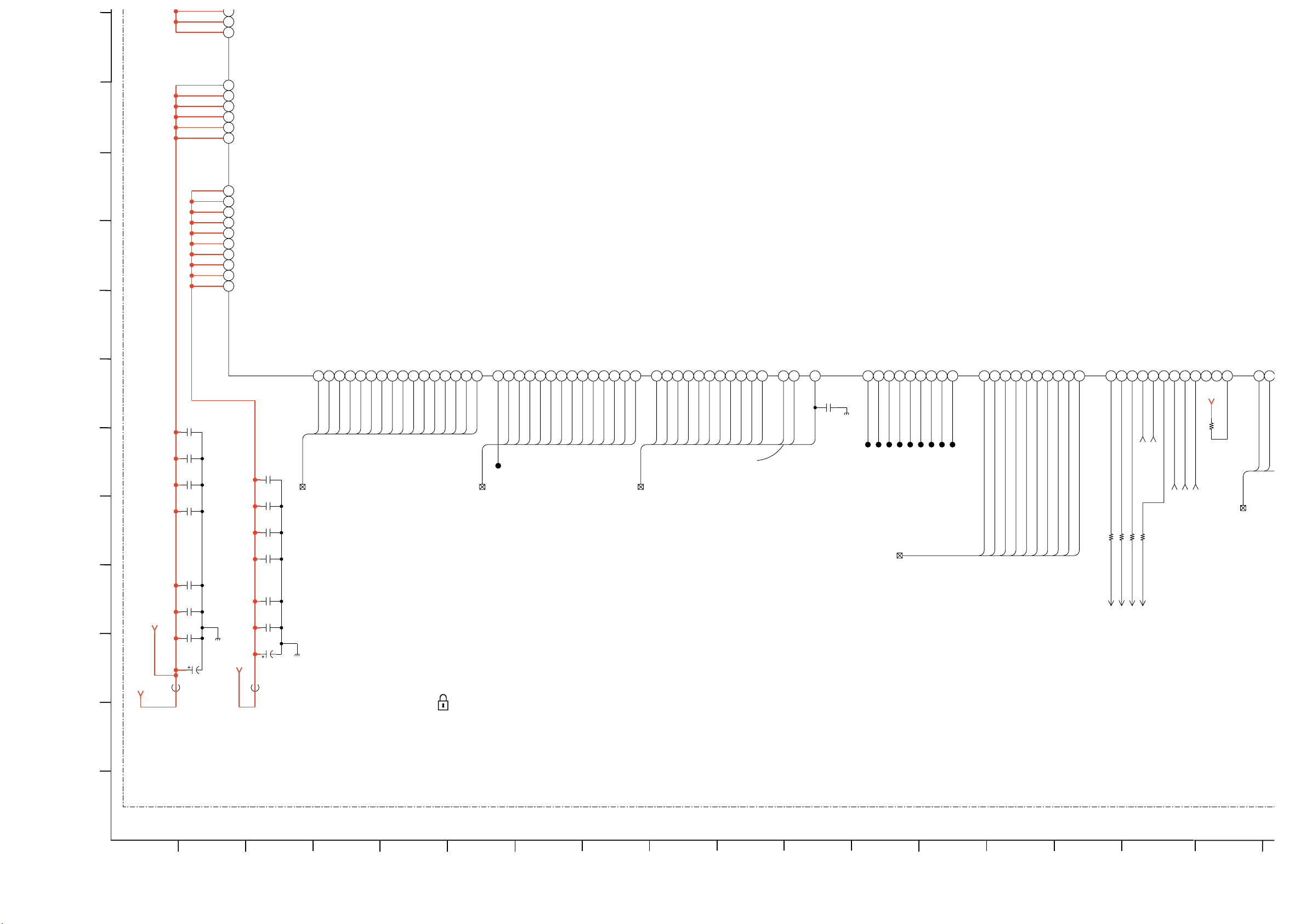
11
_
VDD1
E
FE CI TSCLK
12
E7
VDD1
E6
VDD1
E13
VDD2
E12
VDD2
E11
VDD2
E10
VDD2
E9
VDD2
E8
VDD2
IC7100
13
14
15
16
17
18
19
20
U17
VDD3
U6
VDD3
U5
VDD3
T17
VDD3
G17
VDD3
G5
VDD3
F17
VDD3
F5
VDD3
E17
VDD3
E5
E5 E17 F5 F17 G5 G17 T17 U5 U6 U17 E8 E9 E10 E11 E12 E13 E6 E7 E
VDD3
0.1
C7111
0.1
C7112
0.1
C7113
0.1
C7114
THESE CAPACITORS TO BE PLACED UNDERNEATH BGA
0.1
C7115
FE_+2V5_DDR
FE_+2V5
0.1
C7116
4.7
C7102
FB7101
C7103
XX
0uH
GND_1
C7122
0.1
C7123
0.1
C7124
0.1
C7125
0.1
THESE CAPACITORS TO BE PLACED UNDERNEATH BGA
C7126
0.1
C7127
0.1
C7118
10
3.3V_MAIN
FB7103
0uH
FE_DQ[0-15]
GND_1
DQ15
DQ14
B16
A16
A16
B16
A15
FE_DQ[15]
FE_DQ[14]
FE_DQ[13]
DQ13
DQ12
B15
A15
B15
FE_DQ[12]
DQ11
DQ10
B14
A14
A13
A14
B14
A13
FE_DQ[10]
FE_DQ[9]
FE_DQ[11]
DQ9
DQ8
B13
B13
FE_DQ[8]
FE_DQ[7]
DQ7
D13
D13
C13
FE_DQ[6]
DQ6
C13
D14
D14
FE_DQ[5]
DQ5
DQ4
C14
C14
FE_DQ[4]
FE_DQ[3]
DQ3
D15
D15
FE_DQ[2]
DQ2
DQ1
C15
D16
C15
D16
FE_DQ[1]
B1
DQ0
C16
D12
C16
D12
FE_DQ[0]
SIGN15011
JL7101
FE_DADD[0-12]
1C/13
DADD13
DADD12A9DADD11B9DADD10D8DADD9A8DADD8B8DADD7A7DADD6B7DADD5A6DADD4B6DADD3D6DADD2C6DADD1D7DADD0C7DBA1C8DBA0D9UDQM
C7
A9B9D8
FE_DADD[12]
FE_DADD[11]
FE_DADD[10]
A8B8A7B7A6B6D6C6D7
FE_DADD[3]
FE_DADD[2]
FE_DADD[6]
FE_DADD[7]
FE_DADD[5]
FE_DADD[4]
FE_DADD[9]
FE_DADD[8]
FE_DADD[1]
C8
FE_DADD[0]
FE_DBA1
_DVREF,FE_DWEB
D9
FE_DBA0
A11
A12
A11
A12
FE_DQS1
FE_DQM1
UDQS
LDQM
C11
C11
FE_DQM0
LDQS
C9
C12
C12
FE_DQS0
FE_DCSB
DCSBC9DRASB
DCASB
C10
D10
D10
C10
D11
FE_DRASB
FE_DCASB
FE_DWEB
DWEB
DCKE
DCLK
DCLKB
DVREF
B10
B11
A10
B11
FE_DCLKB
B12
B12
FE_DVREF
D11
B10
A10
FE_DCLK
FE_DCKE
DIFFERENTIAL PAIR
OF CLOCK SIGNALS
FE_M_CKOUT,FE_M_DATA[0-7],FE_M_VAL
GND_1
0.1
C7128
THIS CAPACITOR TO BE
PLACED UNDERNEATH BGA
VDI_D7 / PPORT121
VDI_D6 / PPORT120
VDI_D5 / PPORT119
VDI_D4 / PPORT118
VDI_D3 / PPORT117
VDI_D2 / PPORT116
Y17
V17
AA17
AA17
AA16
TP7113
TP7111
AA16
Y16
Y16
TP7114
Y17
W17
TP7109
TP7108
W17
V17
TP7110
VDI_D1 / PPORT115
VDI_D0 / PPORT114
VDI_VCK / PPORT113
AA15
A1B2A2B3A3
A1
FE_M_DATA[7]
W16
W16
V16
TP7116
TP7117
V16
AA15
TP7118
/ RTS1B
/ CTS1B
STP0_DAT7 / PPORT8
STP0_DAT6 / PPORT7
STP0_DAT5 / PPORT6
STP0_DAT4 / PPORT5
STP0_DAT3 / PPORT4
STP0_DAT2 / PPORT3
STP0_DAT1 / PPORT2
STP0_DAT0 / PPORT1
C4
B4
A4A5D5
B2
A2
B3
A3
C4
B4
A4
FE_M_DATA[3]
FE_M_DATA[6]
FE_M_DATA[5]
FE_M_DATA[2]
FE_M_DATA[0]
FE_M_DATA[1]
FE_M_DATA[4]
STP0_EN / PPORT9
STP0_CLK / PPORT0
REGB / PPORT34
F4N4P2
A5
D5
F4
N4
FE_M_VAL
FE_M_CKOUT
R7121 47
R7123 47
FE_REGB
FE_IOWRB
IOWRB / PPORT31
IORDB / PPORT30
INPACKB / PPORT33
GPIO_VS1B / PPORT28
GPIO_RESET / PPORT32
GPIO_IREQB / PPORT24
G2R2G1K3V1C1Y1
P2
G2
R2
G1
K3
V1
FE_CI1_VS1B
FE_CI1_INPACKB
FE_CI1_IREQB
R7124 47
R7125 47
FE_IORDB
FE_CI1_RSTB
GPIO_CD1B / PPORT26
GPIO_CD2B / PPORT35
PCE1B(CE2B_2) / PPORT36
PCE0B(CE2B_1) / PPORT27
IOSI16B / PPORT25
P3
C1
Y1
P3
E4
B1
B1
E4
3.3V_MAIN
10k
R7128
FE_CI_TSSYNC
FE_CI1_CD1B
FE_CI1_CD2B
FE_CI_TSCLK,FE_CI_TSSYNC,FE_CI_TSVAL
EN / PPORT37
STP1_STRT / PPORT38
STP1
F2
F2
FE_CI_TSVAL
21
22
COMPONENTS MARKED AS XX REFER TO PARTS LIST, WILL ONLY BE LISTED IF FITTED
ABCDEF GH JIKLMN
FE_DBA0,FE_DBA1,FE_DCASB,FE_DCKE,FE_DCLK,FE_DCLKB,FE_DCSB,FE_DQM0,FE_DQM1,FE_DQS0,FE_DQS1,FE_DRASB,FE
O
~ B1 Board Schematic Diagram [ Main Microcontroller, HDMI/AV Side/PC Input, Audio Processor, Scarts ] Page 1C/13 ~
- 23 -
P
Q
 Loading...