

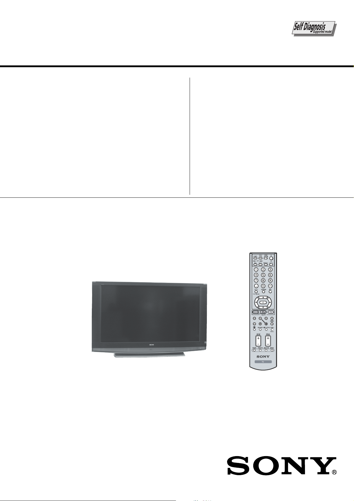
Sony KDF 55WF655K, KDF 60WF655K Service Manual

HISTORY
When clicking an item, it’s detail is displayed.
Model Name: KDF-55WF655K/60WF655K
SERVICE MANUAL
Part No. : 9-872-748-01
Date SUPP./CORR. Description of SUP/COR
2005.3 – NEW –
Change of
main text
SERVICE MANUAL
LA-3
CHASSIS
MODEL COMMANDER DEST. CHASSIS NO.
–––––– –––––––––––– ––––– –––––––––––
KDF-55WF655K
KDF-60WF655K
RM- KD001
RM- KD001
Korea
Korea
MODEL COMMANDER DEST. CHASSIS NO.
–––––– –––––––––––– ––––– –––––––––––
KDF-55WF655K
RM-KD001
LCD PROJECTION TV
Specifications
KDF-55WF655K/60WF655K
RM-KD001 RM-KD001
Power Requirements 220V AC, 60Hz
Power Consumption (W)
In Use (Max) 250W
In Standby Under 20W Less than 1w
Inputs/Outputs HDMI IN
Video - 1080i, 720p, 480p, 480i
Audio - Two channel linear PCM
32, 44.1 and 48 kHz, 16, 20, and
24 bit
Video (IN)
4 total (1 on front panel)
1Vp-p, 75ohms unbalanced, sync
negative
S Video (IN)
4 total (1 on front panel)
Y: 1Vp-p, 75ohms unbalanced,
sync negative
C: 0.286Vp-p (Burst signal),
75ohms
Audio (IN)
7 total (1 on front panel)
500 mVrms (100% modulation)
Impedance:47 kilo ohms
Audio (VAR/FIX) Out
1 total
500 mVrms at the maximum vol
ume setting (Variable)
500 mVrms (Fixed)
Impedance (Output):2 kilo ohm
Note: Audio Out jacks are opera
ble only when the TV’s speaker
is set to Off.
Control S (IN)
1 total
Minijack
Control S (OUT)
1 total
Minijack
Component Video Input
, PR)
2 (Y, P
B
Y : 1.0 Vp-p, 75 ohms unbalanced, sync negative
: 0.7 Vp-p, 75 ohms;
P
B
: 0.7 Vp-p, 75 ohms
P
R
RF Inputs
2 total
Digital Audio Optical Output
(PCM/Dolby Digital)
1 total
Optical Rectangular (1)
Speaker Output (W)
L/R 5W x 2
Woofer 20W
Dimensions (W x H x D)
mm 1,456 x 943 x 491 mm 1,574 x 1,005 x 518 mm
in 57
Mass
kg 46 kg 50.5 kg
lbs 101 lbs 7 oz 111 lbs 5 oz
TruSurround, SRS and the (z)® symbol are trademarks
of SRS Labs, Inc.
TruSurround technology is incorporated under license
from SRS Labs, Inc.
BBE and BBE Symbol are trademarks of BBE Sound,
Inc. and are licensed by BBE Sound, Inc. under U.S.
Patent No. 4,638,258 and 4,482,866.
Manufactured under license from
Dolby Laboratories Licensing
Corporation. Dolby and the double-D
symbol are trademarks of Dolby
Laboratories Licensing Corporation.
KDF-55WF655K KDF-60WF655K
3/8
1/4
x 37
3/8
x 19
in 62 x 39
5/8
x 20
1/2
This TV incorporates High-Definition
Multimedia Interface (HDMI™)
technology. HDMI, the HDMI logo
and High-Definition Multimedia
Interface are trademarks or registered
trademarks of HDMI Licensing LLC.
WEGA, Steady Sound, Digital Reality Creation,
CineMotion, Memory Stick, Memory Stick Duo,
Memory Stick PRO, Memory Stick PRO Duo,
MagicGate, MID and Twin View are trademarks of Sony
Corporation.
in
Design and specifi cations are subject to change without notice.
– 2 –

Television system
(Digital signal with Atsc compliant 8USB is only supported)
American TV standard, NTSC
ATSC compliant 8VSB, ATSC (8VSB terrestrial)
Channel coverage
Terrestrial 2-69/ Cable TV: 1-125 (analog)
Terrestrial: 2-69/ Cable TV: 1-135 (digital)
Screen Size (measured diagonally)
55 inches (KDF-55WF655 Only)
60 inches (KDF-60WF655 Only)
Antenna
75-ohm external antenna terminal for VHF/UHF
Projection System
3 LCD Panels, 1 lens projection system
LCD Panel
0.87 inch TFT LCD panel Approx. 3.28 million dots
(1,042,168 pixels)
KDF-55WF655K/60WF655K
RM-KD001 RM-KD001
Projection Lens
High Performance, large diameter hybrid lens F2.4
Lamp
UHP lamp, 120W, XL-2300
Supplied Accessories
Remote Commander RM-KD001
Two Size AA (R6) Batteries
– 3 –

WARNING!!
AN ISOLATION TRANSFORMER SHOULD BE USED DURING
ANY SERVICE TO AVOID POSSIBLE SHOCK HAZARD, BECAUSE OF LIVE CHASSIS.
THE CHASSIS OF THIS RECElVER IS DIRECTLY CONNECTED
TO THE AC POWER LINE.
SAFETY-RELATED COMPONENT WARNING!!
COMPONENTS IDENTIFIED BY SHADING AND MARK ! ON THE
SCHEMATIC DIAGRAMS, EXPLODED VIEWS AND IN THE
PAR TS LIST ARE CRITICAL TO SAFE OPERATION. REPLACE
THESECOMPONENTS WITH SONY PARTS WHOSE PART NUMBERS APPEAR AS SHOWN IN THIS MANUAL OR IN SUPPLEMENTS PUBLISHED BY SONY. CIRCUIT ADJUSTMENTS THAT
ARE CRITICAL TO SAFEOPERATION ARE IDENTIFIED IN THIS
MANUAL. FOLLOW THESE PROCEDURES WHENEVER CRITICAL COMPONENTS ARE REPLACED OR IMPROPER OPERATION IS SUSPECTED.
KDF-55WF655K/60WF655K
RM-KD001 RM-KD001
– 4 –

KDF-55WF655K/60WF655K
RM-KD001 RM-KD001
Section Title Page
–––––– –––– ––––
1. SELF DIAGNOSIS FUNCTION ................................... 6
2. DISASSEMBLY
2-1. REAR COVER.......................................................... 11
2-2. OU BRACKET ......................................................... 11
2-3. CHASSIS ASSEMBLY AND FAN........................... 12
2-4. SERVICE POSITION ............................................... 12
2-5. POWER SUPPLY BLOCK(LAMP DRIVE UNIT),
OPTICS UNIT BLOCK, T BOARD......................... 13
2-6. RF ANTENNA SWITCH AND P BOARD .............. 13
2-7. U AND H4 BOARDS ............................................... 14
2-8. F BOARD AND G1 BOARD ................................... 14
2-9. A BOARD AND KD BOARD .................................. 15
2-10. Q BOX ASSEMBLY AND B BOARD ..................... 15
2-11. G2 BOARD ............................................................... 16
2-12. WOOFER .................................................................. 16
2-13. D.C. FAN................................................................... 17
2-14. FRONT COVER ASSEMBLY ................................. 17
2-15. HM BOARD AND H2 BOARD ............................... 18
2-16. H1 BOARD ............................................................... 18
2-17. SCREEN MIRROR BLOCK ASSEMBLY .............. 19
2-18. MIRROR COVER ASSEMBLY, H3 BOARD
AND SPEAKER ....................................................... 19
3. WIRE DRESSING ........................................................... 20
4. CIRCUIT ADJUSTMENTS
4-1. SETTING THE SERVICE ADJUSTMENT MODE 24
4-2. SERVICE ADJUSTMENT MODE MEMORY ........ 24
4-3. MEMORY WRITE CONFIRMATION METHOD .. 25
4-4. REMOTE ADJUSTMENT BUTTONS
AND INDICATORS ................................................. 25
4-5. H/V CENTER CONFIRMATION AND
ADJUSTMENT ......................................................... 26
4-6. SERVICE DATA ....................................................... 27
4-7. ID MAP TABLE........................................................ 27
Section Title Page
–––––– –––– ––––
5. DIAGRAMS
5-1. CIRCUIT BOARDS LOCATION ................................. 27
5-2. SCHEMATIC DIAGRAMS AND
PRINTED WIRINGS INFORMATION ........................ 27
5-3. BLOCK DIAGRAM ................................................. 28
5-4. SCHEMATIC DIAGRAMS .......................................... 29
(1) Schematic Diagram of A (1/3) Board ................ 29
(2) Schematic Diagram of A (2/3) Board ............... 30
(3) Schematic Diagram of A (3/3) Board ............... 31
(4) Schematic Diagram of F Board ........................ 32
(5) Schematic Diagram of G1 (1/2) Board ............. 33
(6) Schematic Diagram of G1 (2/2) Board ............. 34
(7) Schematic Diagram of G2 (1/2) Board ............. 35
(8) Schematic Diagram of G2 (2/2) Board ............. 36
(9) Schematic Diagram of H1, H2 Boards ............. 37
(10) Schematic Diagram of H3, H4, HM Boards ..... 38
(11) Schematic Diagram of KD Board ..................... 39
(12) Schematic Diagram of P, T Boards ................... 40
(13) Schematic Diagram of U Board ....................... 41
5-5. PRINTED WIRING BOARDS...................................... 42
• A Board (Component Side) ................................... 42
• A Board (Conductor Side) .................................... 43
• F Board ................................................................. 44
• G1 Board (Component Side) ................................ 45
• G1 Board (Conductor Side) .................................. 46
• G2 Board (Component Side) ................................ 47
• G2 Board (Conductor Side) .................................. 48
• H1, H2, H3 Boards ............................................... 49
• H4, HM Boards ..................................................... 50
• KD Board .............................................................. 51
• P, T, U Boards ....................................................... 52
5-6. SMICONDUCTORS ..................................................... 53
6. EXPLODED VIEWS
6-1. SCREEN MIRROR BLOCK, COVERS .................. 54
6-2. BOTTOM BLOCK ................................................... 55
6-3. MAIN BRACKET-1 ................................................. 56
6-4. MAIN BRACKET-2 ................................................. 57
6-5. OPTICS UNIT BLOCK ............................................ 58
7. ELECTRICAL PARTS LIST ........................................ 59
• A Board ............................................................................... 59
• F Board ............................................................................... 65
• G1 Board ............................................................................. 66
• G2 Board ............................................................................. 69
• HM Board ........................................................................... 72
• H1 Board ............................................................................. 73
• H2 Board ............................................................................. 73
• H3 Board ............................................................................. 74
• H4 Board ............................................................................. 74
• KD Board ............................................................................ 74
• P Board ................................................................................ 77
• T Board ............................................................................... 80
• U Board ............................................................................... 80
APPENDIX ........................................................................... 1
– 5 –

KDF-55WF655K/60WF655K
SECTION 1
RM-KD001 RM-KD001
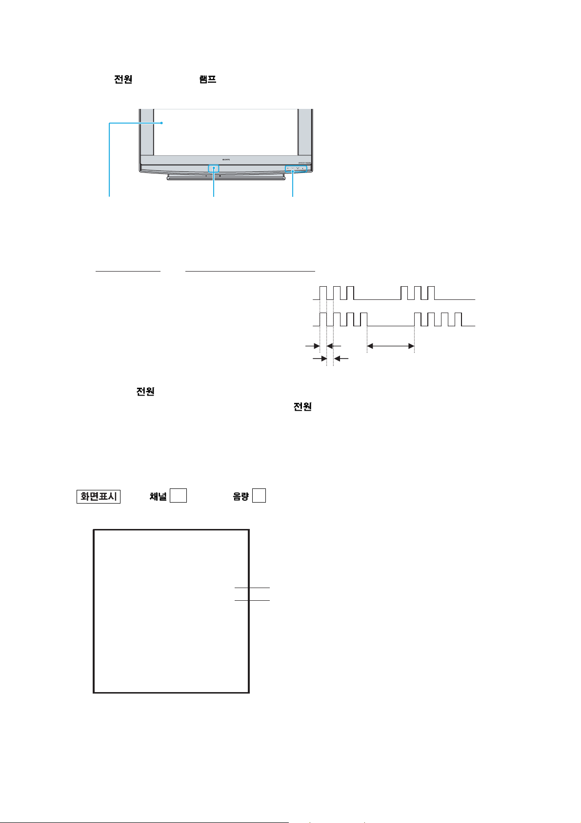
SELF DIAGNOSIS FUNCTION
The units in this manual contain a self-diagnostic function. If an error occurs, the /STANDBY or LED will automatically begin
to flash.
The number of times the LED fl ashes translates to a probable source of the problem. A defi nition of the /STANDBY or LED
flash indicators is listed in the instruction manual for the user’s knowledge and reference. If an error symptom is diffi cult to reproduced
use the Remote
Commander to display the record that is stored at the internal NVM to specify the cause of the failure.
Diagnostic Test Indicators
When an error occurs, the /STANDBY or LED will fl ash a set number of times to indicate the possible cause of the problem.
If there is more than one error, the LED will identify the fi rst of the problem areas. If the errors occur simultaneously, the one that
corresponds to the fewest flashes is identifi ed fi rst.
Results for all of the following diagnostic items are displayed on screen. No error has occurred if the screen displays a “0”.
Diagnostic Item Number of times
Description /STANDBY or LED Probable Cause Detected Symptoms
lamp flashes
Lamp cover error 3 times
Fan error 4 times - Fan connector is not seated securely - No picture/No sound
Temp error 4 times - IIC-E line connector is not seated properly - No picture/No sound
Lamp driver error 5 times - Lamp driver defect - No picture/No sound
Low B error 6 times -No “DD 6V “ output (G1 board) - No picture/No sound
Audio error 7 times
D-OVP error 8 times
ATSC-OVP error 10 times
Lamp error
-LED is ON. - Lamp is dead - No picture/No sound
- Lamp cover is not fastened securely
- Fan1-4 Power is not supplied.(G2 board)
- Fan caught wires or harnesses
- Internal temperature is too high
(WE:H3 board, WF/XS:H4 board)
- Short-circuit of Audio power supply line
(KD board, G1 board)
- Blowout of a fuse
(PS4702,PS4703,PS4704 on KD board)
- IC failure
(IC4703,IC4708,IC4710 on KD board)
- Overvoltage of +3.3V or +2.5V
(A board, B board)
-No “DTL MODULE 5V “ output
(G1 board, G2 board)
- No picture/No sound
- No picture/No sound
- No picture/No sound
- No picture/No sound
– 6 –
Display of /STANDBY or LED Flash Count
LAMP TIMER POWER/STANDBY
KDF-55WF655K/60WF655K
RM-KD001 RM-KD001
POWER
PRO
STD/DUO
Screen
Proj ection l amp
Indicators
-Oneflash is notusedfor self-diagnosis.
-Example
Diagnosis
Number of times LED Flash
Lamp cover 3 times
Fan 4 times
LED ON : 0.3sec
LED OFF : 0.3sec
LED OFF
3.0sec
Releasing the /STANDBY LED Flash
Unplug the power cord from the outlet to temporarily stop the /STANDBY lamp from flashing.
Self-Diagnosis Screen Display
For failures that are diffi cult to reproduce, or accompany occasional power off and/or picture mute, the Self-Diagnosis screen display is
useful to specify the cause.
To Bring Up Screen Test
In standby mode, press the buttons on the Remote Commander sequentially, in rapid succession, as shown below:
1.
Self-Diagnostic Screen Display
t 5 t - t Power ON
SELFCHECK
1:LAMP ERR 0
3:
LAMP COVER 0
FAN-E/TEMP-E 1
4:
5:LAMP DRIVER
0
"1" is displayed when a failure is detected one or more times
"0" is displayed when no failure has been detected
6:LowB-ERR 0
7:Audio-Prot
1
8:D-OVP 0
10 : ATSC_OVP 0
101 : WDT 0
Since the diagnostic results displayed on the screen are not automatically cleared, always check the self-diagnostic screen during repairs.
When you have completed the repairs, clear the result display to “0”.
Note: The self-diagnostic function will not be able to detect any subsequent faults after completion of the repairs unless the result
display is cleared to “0”.
– 7 –

KDF-55WF655K/60WF655K
RM-KD001 RM-KD001
Clearing the Result Display
To clear the result display to “0”, press the buttons on the Remote Commander sequentially when the diagnostic screen is displayed, as
shown below:
1. If the screen is already displayed, proceed to step 3. If not, Power off (Set to Standby model).
2. Press
3. Press
Clearing the Self-Diagnostic Screen
The self diagnosis screen display is cleared by turning off the set using the Remote Commander or the power switch.
Self-Diagnostic Circuit
Self-Diagnosis Function Operation
3 : Lamp cover The rib at the back of the lamp cover closes the SW on the T board to ground pin 3 of
4 : Fan Fan rotation is detected by “FAN-PROT” and the DE-micro (pin 92 of IC6902) turns off the
4 : Temp When the temperature sensor on the H3 board (WE models) or H4 board (WF/XS models)
5 : Lamp driver When the “LAMP-PROT” (pin 95) is low, the lamp is not turned on. If the “LAMP-HV-
6 : Low B error When no “DD 6V “ is detected, pin 129 of TV-micro is low and it turns off the main power.
7 : Audio When DC voltage is detected at the speaker or woofer outputs, pin 128 of TV-micro is low
8 : D-OVP When overvoltage of “+3.3V” or “+2.5V” is detected, pin 126 of TV-micro is low and it
10 : ATSC-OVP When no “Digital Module 5V” is detected, pin 127 of TV-micro is low and it turns off the
LAMP : Lamp When the “LAMP-PROT” (pin 95) is low, the lamp is not turned on. If the “LAMP-HV-
t 5 t – t 1 ON
8 t ENTER
CN8001.
It is monitored by the DE-micro (pin 94 of IC6902) and turns off the lamp when it is opened.
lamp when it is “high”.
detects high temperature, or IIC-E line connector (CN6022:G2 board, CN44:H3board/
H4board) is not seated securely, the DE-micro turns off the lamp.
DET”(pin 96) is low at the same time, it is classified as no high voltage of the lamp driver.
and it turns off the main power.
turns off the main power.
main power.
DET” (pin96) is high at the same time, it is classified as no lamp or a dead lamp.
– 8 –

Self-Diagnosis Block Diagram
H4 board
IC41
Temp
4:Temp
sensor
KD board
Audio
amp
A board
+3.3V
7:Audio
8:D-OVP
+2.5V
G1 board
DD6V
6:LowB
error
DTL5
IC6902
Display Engine u-com
IIC-E
LAMP-COVER
LAMP-PROT
LAMP-HV-DET
CN6029
23
CN6020
C26
CN6029
23
CN6006
G2 board
FAN PROT
IIC-WE
92
94
95
96
CN6017
4:Fan
11
14
13
14
A8
A14
B14
16
CN6000
2
5
8
CN6022
8
CN6019
12:ATSC
CN6023
515
FAN1-PRT
FAN2-PRT
FAN3-PRT
FAN4-PRT
3:Lamp cover
5:Lamp
driver
OVP
KDF-55WF655K/60WF655K
RM-KD001 RM-KD001
Fan1
Fan2
Fan3
Fan4
T board
S8001
SW
Lamp driver
HV-DET
B
IC3801 WE u-com
IIC-WE
IIC-TV
IC3604 TV u-com
IIC-TV
SP_DC_PROT
128
126
D_OVP
LB_ERROR
129
127
ATSC_OVP
Digital Box
DTL MDL5V
Lamp
– 9 –

KDF-55WF655K/60WF655K
RM-KD001 RM-KD001
Reading Lamp and Panel time
Use the following to determine the lamp and panel time of a set.
Screen Display Method
In standby mode, press the buttons on the Remote Commander sequentially, in rapid succession, as shown below:
+
1. Press
2. To enter the DE-micro service menu, press
3. To display the Lamp time, press
5
2
ex am ple
PANEL NVM OK 9 OPTION_E
0 LAMP 0 Diff
Lam pTM 14 Lam pCT 71
The screen displays:
“T
otal lamp time is 14 hours” and “T
9 times.
otal lamp ON/OFF cycle is 71 times”
3 times.
1
Power ON
To reset the lamp time press
WRI-EXE(Character color is Red) is momemtarily displayed and LampTM is
reset to “0”.
4. To display the Panel time, press
3
1
7 times
.
ex am ple
PANEL NVM OK 9 OPT ION_E
7 SH SFT1 10 Diff 1
PanelTM 14h
The screen displays:
“T
NOTE: You cannot reset the Panel time with the Service menu.
otal Panel time is 14 hours”
Exiting Service Mode
After completing the changes exit service mode by turning off the set using the Remote Commander or the power switch.
– 10 –

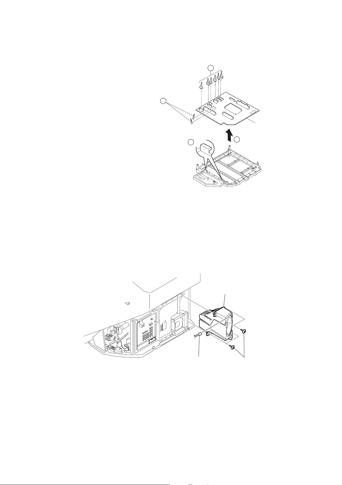
2-1. REAR COVER
KDF-55WF655K/60WF655K
RM-KD001 RM-KD001
SECTION 2
DISASSEMBLY
Rear cover
2-2. OU BRACKET
4
6 OU bracket
1
Thirteen screws
(+BVTP 4x16)
1 Screw
(+BVTP 4x16)
2 Two screws
(+BVTP 4x16)
5 Three
fasten tags
– 11 –
3 Two screws
(+BVTP 4x16)
2-3. CHASSIS ASSEMBLY AND FAN
4 Chassis assembly
3
2 Side stay (R)
6 Fan bracket (chassis)
with DC fan
1 Screw
(+BVTP 4x16)
KDF-55WF655K/60WF655K
RM-KD001 RM-KD001
5 Three screws
(+PTPWH 4x16)
2-4. SERVICE POSITION
Chassis assembly
Pull back on claw, then gently pull out chassis assembly
1
– 12 –

KDF-55WF655K/60WF655K
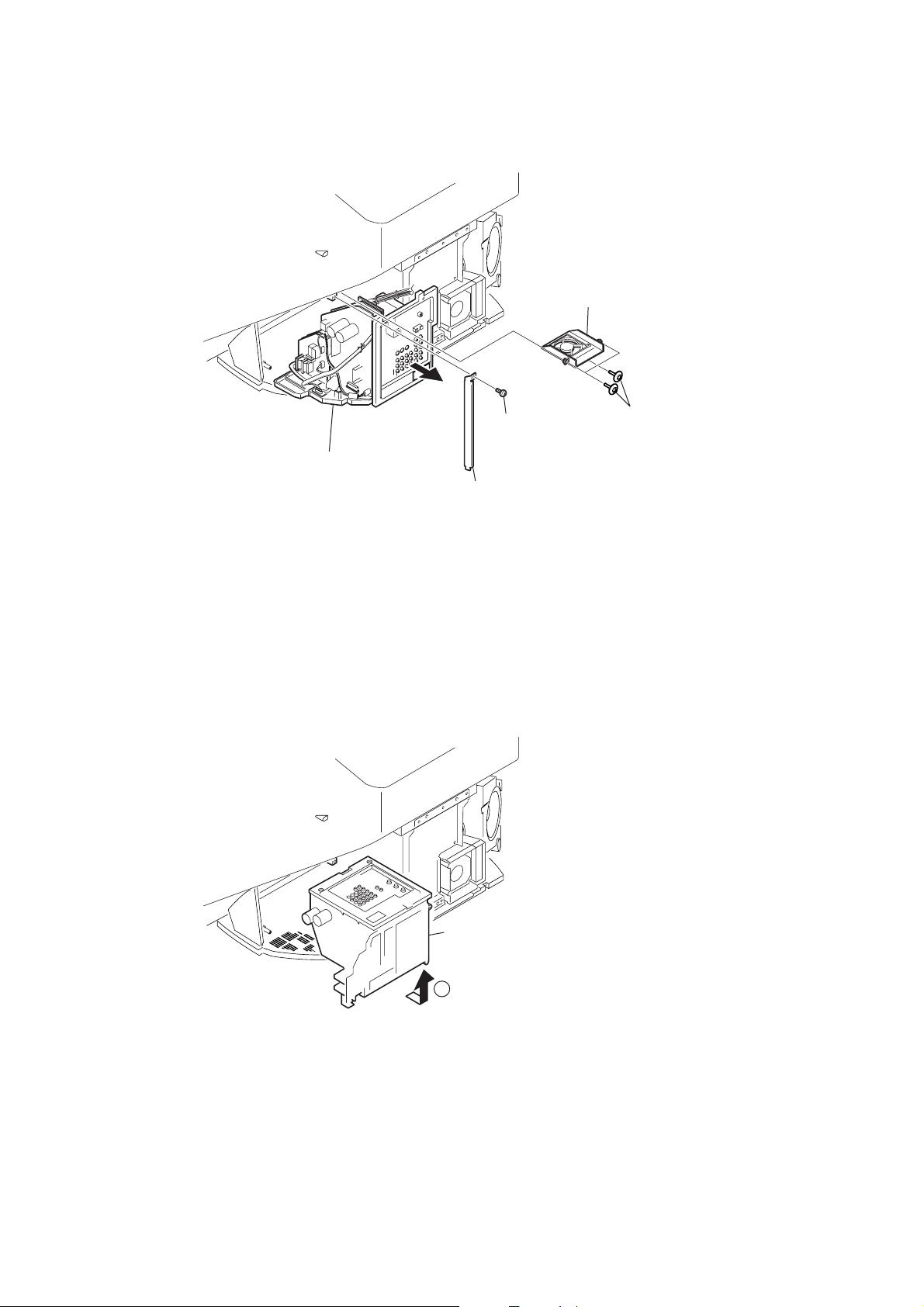
2-5. POWER SUPPLY BLOCK (LAMP DRIVE UNIT), OPTICS UNIT BLOCK, T BOARD
CAUTION: When removing the Power Supply Block be careful not to move the Optics Unit Block
RM-KD001 RM-KD001
qa T board
CAUTION: When removing the Power Supply Block
be careful not to move
the Optics Unit Block
1 Remove the duct fan bracket with DC fan
3 Two screws (+PWH 4x16)
4 Unhook the
antenna cable
7 Power
supply
block
2 Disconnect two connectors
(to detach the cables from the
Optics Unit Block Assembly)
6
5 Four screws
(+BVTP 3x12)
2
5
6 Optics unit block assembly
(with power supply block)
0 Screw
(+BVTP 3x12)
9 Duct fan bracket 2
8
7 Two screws
(+BVTP 4x16)
3 Duct fan bracket
with DC fan
1 Screw
(+BVTP 4x16)
4 Loosen two screws
2-6. RF ANTENNA SWITCH AND P BOARD REMOVAL
Disconnect one connector
and the ground wire
Two screws
7
6
(+BVTP 3x12)
P board
4
U bracket
5
RF antenna switch
Two hexagonal nuts
1
Screw (+PSWM 3x8)
2
Six Screws (+BVTP
3
3x12)
– 13 –

2-7. U AND H4 BOARDS
9
4
G1 board
5
Gently pull back on the three clips
on the pin connection slots
while slowly lifting the G1 Board.
Disconnect two connectors
(CN1601 and CN1602)
and one ground wire (CN1607)
Remove one screw
(+BVTP 3X12 TYPE2)
Disconnect two connectors
(CN1908 and CN1909)
and two ground wires
(CN1902 and CN1903)
Disconnect two connectors (CN1603 & CN1604)
8
Unfasten three Circuit Board Supports
Remove wires from purse locks
2
Disconnect the Power cord
from CN1900 connector.
7
3
1
6
Pull F Bracket out
and up to remove
Claw
KDF-55WF655K/60WF655K
RM-KD001 RM-KD001
One screw
(+BVTP 3X12)
2-8. F BOARD AND G1 BOARD
Gently pull back on tab to
release U board
2
3
Gently pull back on tabs
to release H4 board
1
U board
– 14 –

2-9. A BOARD AND KD BOARD
Disconnect three connectors
(CN4701, CN4705, and CN4702)
KDF-55WF655K/60WF655K
RM-KD001 RM-KD001
5
Disconnect three connectors
3
(CN8003, CN8004, and CN8008)
and coax cable from tuner
Unfasten two Circuit Board Supports
Gently pull back
4
2
on the three clips
on the Pin Connection slots
while slowly lifting the A board
A board
Remove cables
1
from purse locks
2-10. Q BOX ASSEMBLY AND B BOARD
KD board
Gently pull back
6
on the two clips
on the Pin Connection slots
while slowly lifting the KD board
Disconnect six connectors
Unplug two coax cables
connected to the antenna switch
Remove four screws
(+BVTP 3X12)
6
Remove two screws
8
(+BVTP
7
3X12 TYPE2)
Remove cables from purse locks
5
Q Box Assembly
Remove two connectors
9
2
(CN3501 and CN3502)
1
Remove cables from purse
B board
Remove two screws
3
(3X12), + BVWHTP
Gently pull back
4
on the two clips
on the Pin Connection slots
while slowly lifting the B board
– 15 –
2-11. G2 BOARD
KDF-55WF655K/60WF655K
RM-KD001 RM-KD001
Disconnect 6 connectors
(CN6000, CN6024,
CN6028, CN6021,
CN6023, and CN6022)
Disconnect 2 ground wires
(CN6013 and CN6015)
Gently pull back on the two clips
while slowly lifting the G2 Board.
2
1
G2 board
3
3
2-12. WOOFER
3 Woofer block assembly
1 Connector
2 Four screws
(+PTPWH 4x16)
– 16 –
2-13. D.C. FAN
KDF-55WF655K/60WF655K
2
Three screws
(+BVTP 3x12)
1
Disconnect two connectors
3
D.C. Fan
Optics Unit block assembly
RM-KD001 RM-KD001
2-14. FRONT COVER ASSEMBLY
Three screws
(+BVTP 3X12 TYPE2)
Gently pull the
Front cover assembly forward.
Note the area of the 3 magnets
holding the cover
1 Two ornamental screws
Cable Cover
2
3
One screw
(+BVTP 3X12)
2-14-2. REPLACING THE LAMP
For detailed instructions on replacing the lamp, see
Page 16 of the Operating Instructions manual.
– 17 –

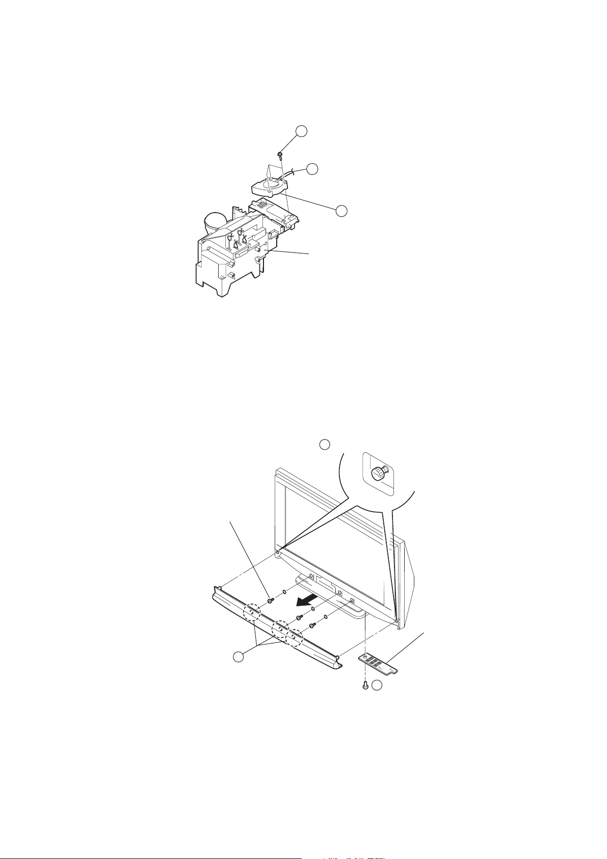
2-15. HM BOARD AND H2 BOARD
1
Two screws
(+BVTP 3X12 TYPE2)
Two screws
(+BVTP 3X12 TYPE2)
Pull back on the clip
while lifting the HM board up
HM board
Disconnect one connector
(CN7301)
One screw
(+BVTP 3x12)
Disconnect one connector
(CN4502)
2
3
5
6
Disconnect USB cable
4
6
H2 board
KDF-55WF655K/60WF655K
RM-KD001 RM-KD001
2-16. H1 BOARD REMOVAL
Disconnect one connector
Screen mirror block assembly
3
H1 board
H1 board
H1 button
H1 bracket
– 18 –
Gently pull back on the bottom tab
4
of the H1 bracket then slide out the H1 board
One screw
2
(+BVTP 4x16)
1
Using tweezers gently detach the
H1 Bracket Cap
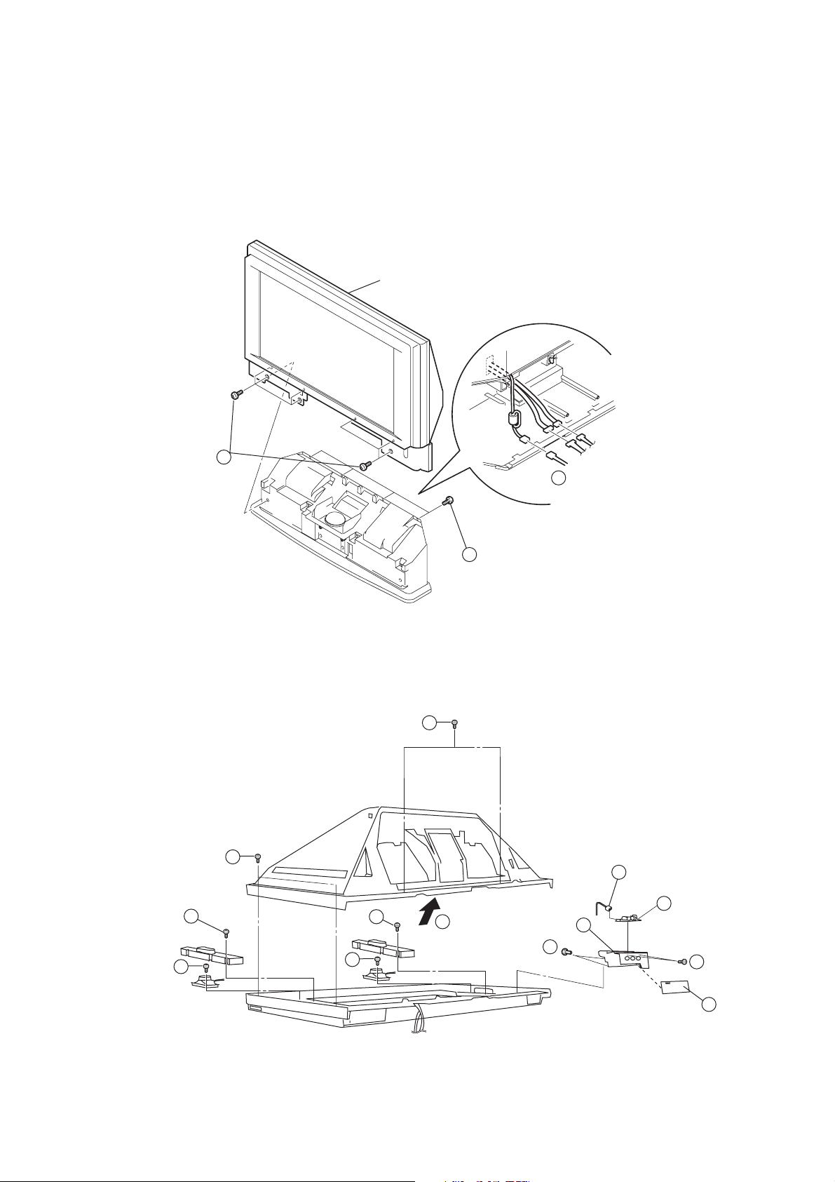
KDF-55WF655K/60WF655K
RM-KD001 RM-KD001
2-17. SCREEN MIRROR BLOCK ASSEMBLY
Caution:
When repairing anything inside the Screen Mirror Block Assembly be sure to clean the mirror and Diffusion Plate
to remove any dust particles.
Note: Be sure to remove the screws that secure
the reinfocement plates (R)/(L).
Screen mirror block assembly
Seven screws
(+BVTP 4x16)
3
2
Four screws
(+BVTP 4x16)
2-18. MIRROR COVER ASSEMBLY, H3 BOARD AND SPEAKER
Four screws
2
(+BVTP 4X16)
Sixteen screws
(+BVTP
4X16)
1
1
Disconnect three connectors
11
Disconnect one connector
Eight screws
(+BVTP
4X16)
Four screws
(+BVTP 4X16)
10
4
5
4
5
3
Lift bracket out
Two screws
(+BVTP 4x16)
7
6
Lift H3 board up,
then pull back to remove
from bracket
9
Two screws
(+BVTP 4x16)
8
Remove H3
Bracket door
– 19 –

[F] EMI Shield wire around
2nd post
KDF-55WF655K/60WF655K
RM-KD001 RM-KD001
SECTION 3
WIRE DRESSING
Make sure purse lock is
completely seated to [G1]
Tie btwn 1st & 2nd posts
Blk/Wht to the right
Use Coated Lead Pin to keep
wires from migrating into
Primary Ckt
Make sure Coated Lead
Pin does not touch
[G1] heat sink
USB cable must stay to right
side of [B]
[KD] wires are secured to free
purse lock, not ATSC Box
Make sure 8 pin connector is
fully seated
– 20 –
LVDS Cables dresses behind
purse lock
KDF-55WF655K/60WF655K
RM-KD001 RM-KD001
Emi Tape added to Sub Tuner
cable
Detail of front side ATSC Box
Detail of front side [G1] All wires through purse lock
Detail of front side ATSC Box [C1] LVDS dressing
Top connector wires must be to
the left of lower wires
Detail of USB around ATSC
Box Area
Bend GND tab after wire is
installed
USB Cable must not touch
metal grill for EMI issue
– 21 –
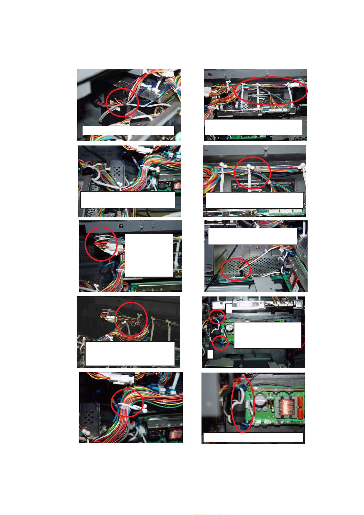
Tape must avoid OP Block Label
KDF-55WF655K/60WF655K
RM-KD001 RM-KD001
Sensor wire should be in left
three purse locks
Purse Lock must be to the right of
the cable tie position
Front side
harnesses
dressed
through bottom
block purse lock
Front side harnesses dressed
behind the 1st [C1] purse lock &
secured with free purse lock
Loop sensor wire at the 2nd purse
lock position
Clip position move to avoid wire
touching Emi Shield
2
Dress Drvr harness
through bottom coated
lead pin then the top
1
Left Side Coated Lead Pins details
– 22 –
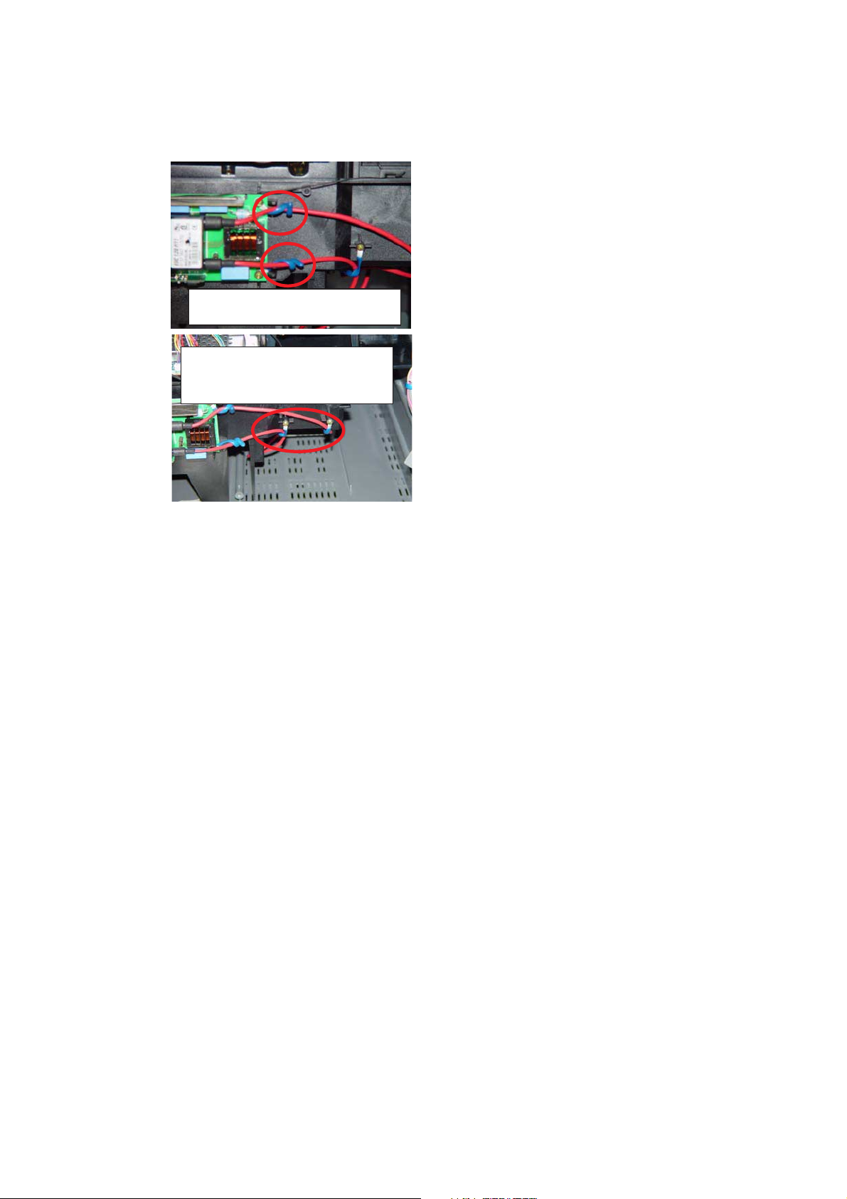
Right Side Coated Lead Pins
details
Twist Coated Lead inward to
avoid contact with fan assembly
after installation
KDF-55WF655K/60WF655K
RM-KD001 RM-KD001
– 23 –

SECTION 4
CIRCUIT ADJUSTMENTS
4-1. SETTING THE SERVICE ADJUSTMENT
MODE
To adjust various set features, use the Remote Commander to put the
set into service mode to display the service menus.
1. TV must be in standby mode. (Power off).
2. Press the following buttons on the Remote Commander within a
second of each other:
The first service menu (TV) displays.
3. To display the service menu that contains the category you want
to adjust, press on the Remote Commander.
(Refer to Service Menus)
Service Menu
t 5 t + t 1 .
Category
Ircnmetne
ste sp
TV
VERSION
CXA2209Q
AP
DLBY
BUSSW
CXA2103
CXA2163
2DCOMB
Q BOX
QM
QT
KDF-55WF655K/60WF655K
RM-KD001 RM-KD001
SERVICE MENUS
(CATEGORIES ONLY)
WEM 2
(WEGA ENGINE)
DCP-INT
DCP-OSD
DCP-BLK
DCP-ADJ1
DCP-ADJ2
DCP-USER
DCP-AVP
MID-1-9
PANEL
(DISPLAY ENGINE)
OP
A7001R
A7001G
A7001B
GB_RGB
FAN_CNT1
FAN_CNT2
TEMP
PANEL NVM OK 1 5D089T9PN
41RLVL_
Item #
H
4590
Data value
D
i ff1
Adjustment
item
Sample Panel (Display Engine) Service Menu
4-2. SERVICE ADJUSTMENT MODE MEMORY
The screen displays the • rst category in the selected service menu.
4. To change the category, press 2 or 5 on the Remote Com-
mander.
Note: Pressing 2 or 5 only changes the categories within the
service menu displayed. To change a category on one of the other
service menus, press the
menu is displayed.
5. To change the adjustment item, press 1 or 4 on the Remote
Commander.
6. To change the data value, press 3 or 6 on the Remote Com-
mander.
Note: To go back to the last saved data value, press - then
on the Remote Commander to read the memory.
7. To write into memory, press
Remote Commander.
8. To exit service mode, turn the power off.
button until the correct service
then on the
TELETEXT
MSP SIZE
MSPMD
MSPSEL
MSPFNC
MSP3714G
CCPS (1-11)
DELAY (1-2)
OSD
CC M
CC S
CC T
ID
OPB GA
OP GA
OP US
SNNR
SNSS
DRCVR
USER-NR
LPFC
CCPM-1 (1-12)
OVSN
OP
OSD_E
OPTION_E
S_MAS_M
S_MAS_S
J_L004
D9809_1
D9809PIC
D9809TPN
D9809CUR
D9809TG1
D9809 OSD
D9809HPF
D9809CSC
D9809CGA
D9809HUE
IMG_SHFT
PROT_CNT
– 24 –

KDF-55WF655K/60WF655K
RM-KD001 RM-KD001
4-3. MEMORY WRITE CONFIRMATION METHOD
1. After completing all adjustments turn the set off with the Remote Commander and WAIT for the fans to turn off before proceeding to the
next step.
Note: It may take up to two minutes for the fans to stop.
Caution: To avoid over heating the lamp, do not unplug the set until the fans have stopped.
2. After the fans have stopped, unplug the set from the AC outlet, then plug the set back in the AC outlet.
3. To verify the changes repeat steps 2 through 5 from sections 2-1. Setting the Service Adjustment Mode and 2-2. Service Adjustment Mode
Memory.
4. To exit service mode, turn the power off.
Note: To restore the User Controls and Channel Memory settings to the preset factory conditions, put the set into service mode (step
2 from 2-1. Setting the Service Adjustment Mode), then press 8 then
display the initial setup screen.
4-4. REMOTE ADJUSTMENT BUTTONS AND INDICATORS
Write into
memory
Adjustment
item up
1
on the Remote Commander. The set will restart and
1
3
Data value up
Category up
Adjustment
item down
Restore User Control
and Channel Memory
2
4
8
(+)
6 Data value down
5 Category down
Display Service Menue
RM-KD001
– 25 –

KDF-55WF655K/60WF655K
RM-KD001 RM-KD001
4-5. H/V CENTER CONFIRMATION AND ADJUSTMENTS
Please check the picture horizontal/vertical center after the replacement of the Optics Unit Block Assembly or any part of the Top assembly.
1. Check the H/V center with 480i monoscope signal in “Full” mode.
2. If the center is shifted, adjust using the following service items:
NOTE: Please record the steps shifted as MDHP and MDVP .
MID-X1 9 MDHP (for H center)
10 MDVP (for H center)
MDVP
MDHP
3. Change the WIDE mode to “Normal” and change the register data as follows:
MID-X1 9 MDHP + MDHP
(Don’t change the MDVP data)
4. Display the Twin Picture with the “split” button of the remote commander and change the registers data as follows:
MID-X1 9 MDHP + MDHP
10 MDVP +
5. Press “Favorites” button and change the registers data as follows:
MID-X1 9 MDHP +
10 MDVP +
MDVP
MDHP
MDVP
6. OSD horizontal position must be adjusted as follows:
If above sum exceeds 255, set 1 to “16 RP1H” and set the “sum-256” to “17 RP1L”.
Since the registers are different from other cases, be careful to follow complete instructions, and write the data before changing the
display/ wide mode .
4-6. SERVICE DATA
Please refer to the appendix for details.
– 26 –
SECTION 5
(
)
DIAGRAMS
5-1. CIRCUIT BOARDS LOCATION
T
Q Box
H2
Assembly
H1
G1
G2
H4
F
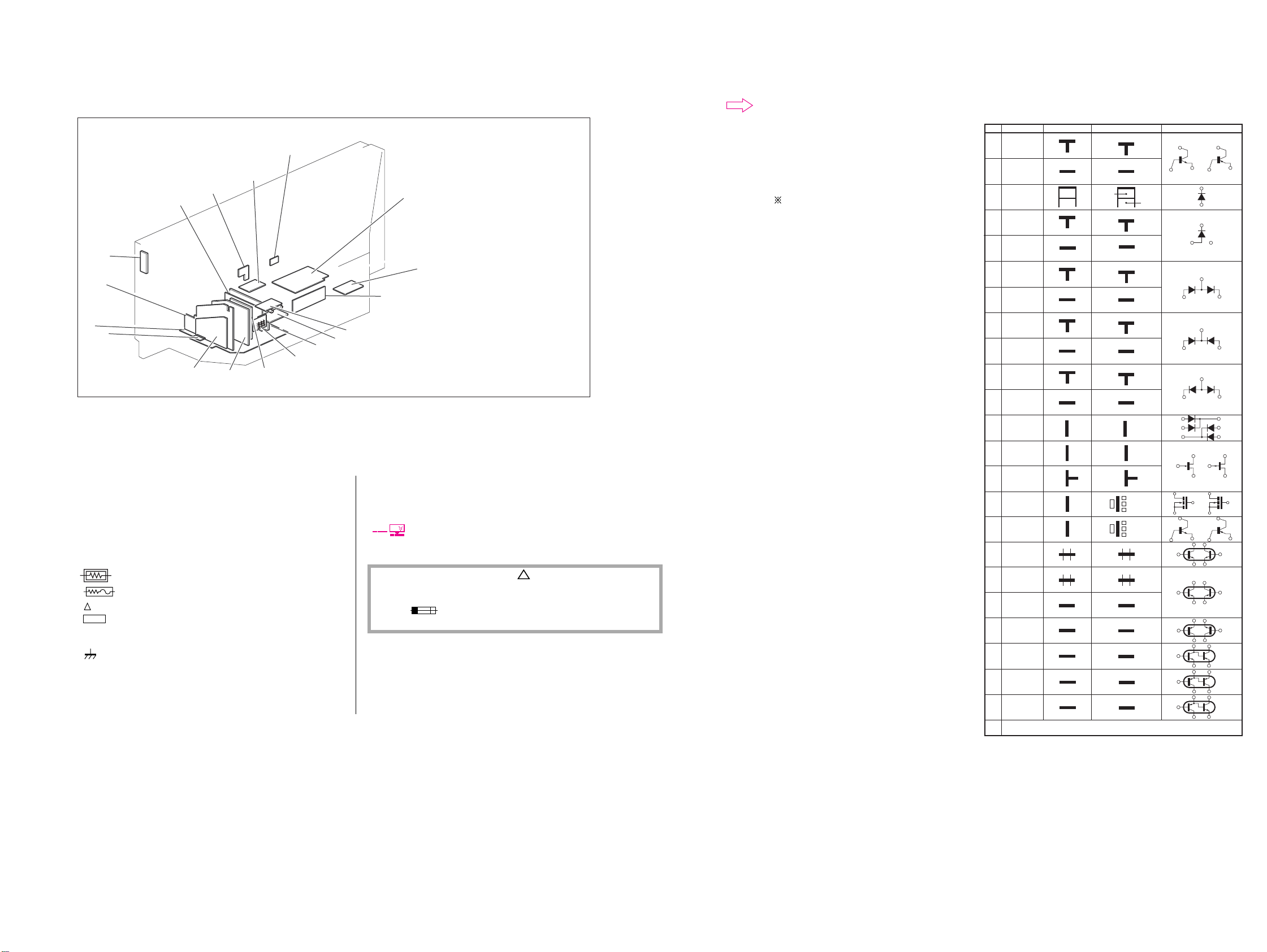
5-2. SCHEMATIC DIAGRAMS AND PRINTED WIRINGS INFORMATION
Note:
• The parts marked “#” on schematic diagrams are not mounted.
• All capacitors are in µF unless otherwise noted. pF : µµF 50WV or
less are not indicated except for electrolytics and tantalums.
• All electrolytics are in 50V unless otherwise specifi ed.
• All resistors are in ohms. kΩ=1000Ω, MΩ=1000kΩ
Indication of resistance, which does not have one for rating
electrical power, is as follows: Pitch : 5mm
• 1/ 4 W in resistance, 1/10 W and 1/16 W in chip resistance.
•
: nonflammable resistor.
•
•
•
: fusible resistor.
: internal component.
: panel designation and adjustment for repair.
• All variable and adjustable resistors have characteristic curve B, unless otherwise noted.
•
: earth-chassis.
• Readings are taken with a PAL color-bar signal input.
• Readings are taken with a 10MΩ digital multimeter.
•Voltages are dc with respect to ground unless otherwise noted.
Rating electrical power :
HM
C (Part of Optics Unit Block Assembly
Cannot be ordered separately)
H3
Power supply
bloc k
RF antenna switch
P
B
U
A
KD
1
/ 4 W
•Voltage variations may be noted due to normal production tolerances.
• All voltages are in V.
: Measurement impossibillity.
S
• Circled numbers are waveform references.
• A : B+line.
• : B-line (Actual measured value may be different).
The components identifi ed by shading and
only with part number specifi ed.
The symbol indicates a fast operating fuse and is displayed on the component
side of the board. Replace only with fuse of the same rating as marked.
!
symbol are critical for safety . Replace
•
: signal path.(RF)
Reference information
RESISTOR : RN METAL FILM
: RC SOLID
: FPRD NONFLAMMABLE CARBON
: FUSE NONFLAMMABLE FUSIBLE
: RW NONFLAMMABLE WIREWOUND
: RS NONFLAMMABLE METAL OXIDE
: RB NONFLAMMABLE CEMENT
ADJUSTMENT RESISTOR
:
COIL : LF-8L MICRO INDUCTOR
CAPACITOR : TA TANTALUM
: PS STYROL
: PP POLYPROPYLENE
: PT MYLAR
: MPS METALIZED POLYESTER
: MPP METALIZED POLYPROPYLENE
: ALB BIPOLAR
: ALT HIGH TEMPERATURE
: ALR HIGH RIPPLE
KDF-55WF655K/60WF655K
RM-KD001 RM-KD001
Terminal name of semiconductors in silk screen
printed circuit ( )
Device Printed symbol Terminal name
Transistor
1
Transistor
2
3
Diode
4
Diode
Diode
5
Diode
6
Diode
7
8
Diode
Diode
9
Diode
0
Diode
qa
Diode
qs
Transistor
qd
(FET)
Transistor
qf
(FET)
Transistor
qg
(FET)
Transistor
qh
Transistor
qj
Transistor
qk
Transistor
ql
Transistor
w;
Transistor
wa
Transistor
ws
Transistor
wd
Discrete semiconductot
–
Chip semiconductors that are not actually used are included.
*
Collector
Base
Collector
Base
Cathode
Cathode
Anode
Cathode
Anode
Common
Anode
Common
Anode Cathode
Common
Anode
Common
Anode Anode
Common
Cathode
Common
Cathode
Anode
Anode
Cathode
Drain
Drain
B1 E1C2
B2 C1
E2
B2 E2C1
B1 C2
E1
B2 E2
C1
B1 C2
E1
B2 E2
C1
B1 C2
E1
E2
B1 E1
C2
(B2)
E1
B1
C1
(B2)
E1
E2
C2
Emitter
Emitter
Anode
(NC)
(NC)
Cathode
Anode
Cathode
Cathode
Cathode
Anode
Anode
Source
Gate
Source
Gate
Source
Drain
Gate
Emitter
Collector
Base
C1(B2)
E2
C2
B1
C1
Circuit
D
G
D
S
B1
B1
B1
B1
B1
B1
D
G
S
S
D
G
C1
E1
C1
E1
E1
C1
E2
C1
C1
G
S
C2
B2
E2
C2
B2
E2
E2
B2
C2
C2C1(B2)
E2
E2E1(B2)
C2
C2E1(B2)
C2
Ver.1.5
– 27 –
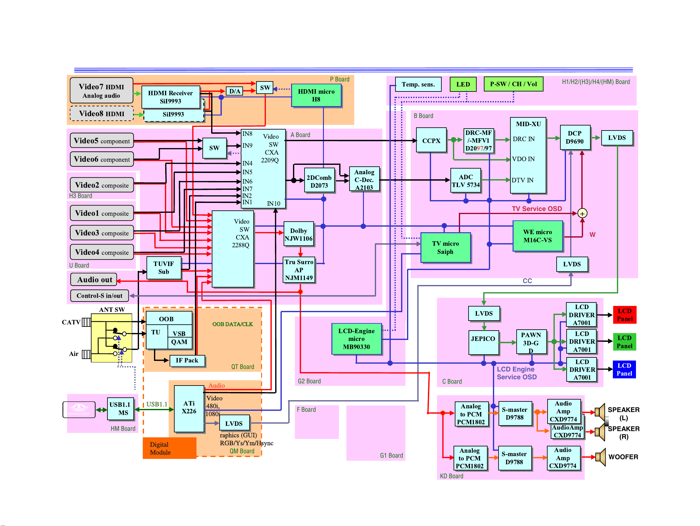
5-3. BLOCK DIAGRAM
KDF-55WF655K/60WF655K
RM-KD001 RM-KD001
$
H3 Board
"
#
U Board
/
&'(
&'(
)))"
)))"
&'(
&'(
)))"
)))"
%
%
+
!
%
!
*(
*(
A Board
,*
8
-7% 1
( ((
-7 #)
$
$
1"
P Board
,0!
1"
B Board
,,
.4*3! 22!
&,0
+0
1)+)
,
. "#
*(
*(
35
35
GUI Graphics / Analog CC
0% + , +
0
TV Service OSD
%4 *(
%4 *(
,0
,0
H1/H2/(H3)/H4/(HM) Board
,
))1
.
.
+
WE
Service OSD
.
.
,/(0 +/
,
(
Memory Stick
- %
!
h
HM Board
USB1.1
Digital
Module
" #$%
QT Board
Audio
Video
480i, 480p, 720p,
1080i
.
raphics (GUI)
RGB/Ys/Ym/Hsync
QM Board
G2 Board
F Board
.,04
.,04
*(
*(
)1""1
)1""1
G1 Board
C Board
, $1
, $1
KD Board
.
74,
/ ,
/ ,
.
%-
"06
LCD Engine
Service OSD
0*2/(
)$$
0*2/(
)$$
&4&
&4&
&4&
*3
,)#
*3
,)#
*3
,)#
.,
11
.,
11
.,
11
.,
.,
.,
SPEAKER
(L)
SPEAKER
(R)
WOOFER
– 28 –
5-4. SCHEMATIC DIAGRAMS
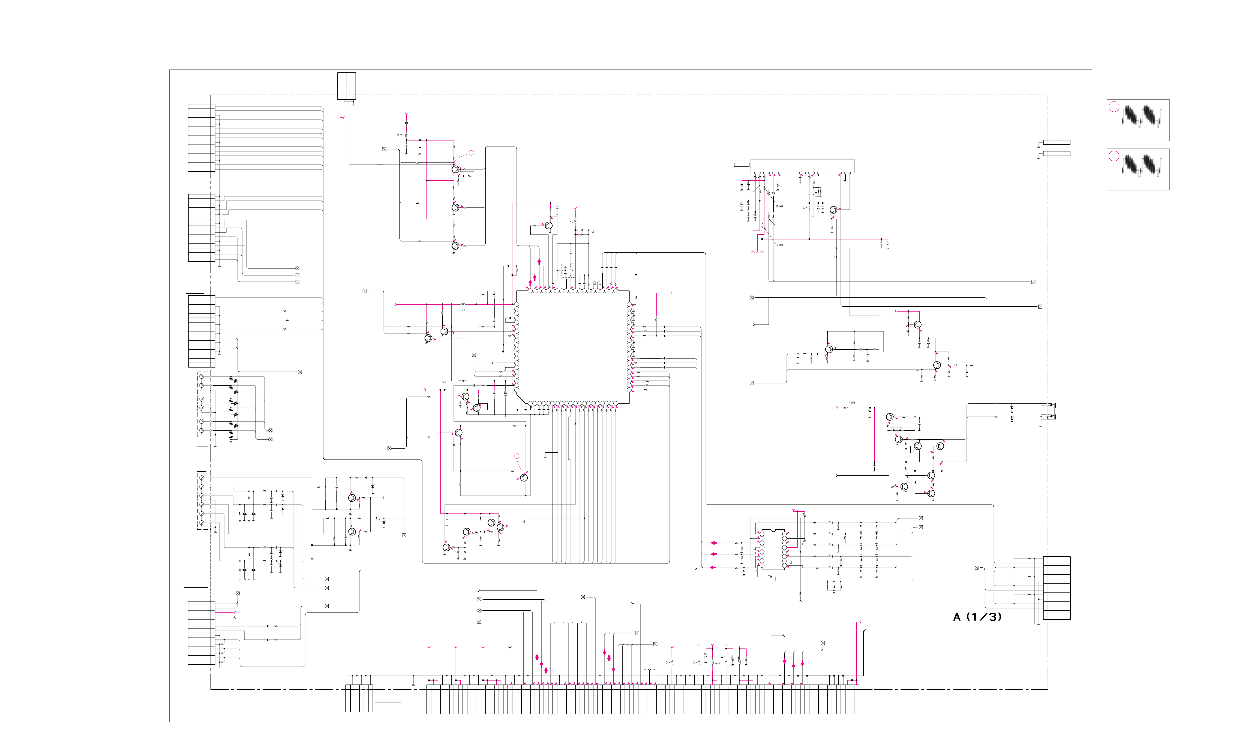
(1) Schematic Diagram of A (1/3) Board
1 | 2 | 3 | 4 | 5 | 6 | 7 | 8 | 9 | 10 | 11 | 12 | 13 | 14 | 15 | 16 | 17 | 18 | 19 | 20 | 21 | 22 | 23
TO U:CN9401
CN8002
B-TO-B
B-TO-B
15P
TO U:CN9402
CN8001
15P
Y1
C1
GND
Y3
GND
C3
S3
Y4
GND
C4
S4
V1-S2
GND
V3-S2
V4-S2
GND
V1
GND
V3
GND
V4
GND
L1
L3
L4
GND
R1
GND
R3
R4
1
2
3
4
5
6
7
8
9
10
11
12
13
14
15
1
2
3
4
5
6
7
8
9
10
11
12
13
14
15
A
—
B
—
C
—
D
—
E
—
CN8003
B16B-XADSS-N-A
F
—
G
—
H
—
I
—
TO H3:CN43
J8002
6P
V2-SW
V2-S2
E
V2-C
E
V2-Y
E
V2-V
E
V2-L
V2-R
E
VIDEO 56
SIGNAL
1
2
3
4
5
6
7
8
9
10
E
11
12
13
14
15
16
L1
R1
L2
R2
VD8013
VD8017
VD8014
VD8018
VD8015 R8190
VD8016
VD8024
J
VIDEO 56
AUDIO
—
K
R1
R2
—
J8004
6P
L
—
M
TO P:CN9504
—
N
—
O
CN8004
B14B-XADSS-N-A
SCLK
SDAT
9V
HDMI-RESET
A-GND
R
L
GND
PR
GND
PB
GND
Y
GND
IIC-TV
SCL
1
SDA
2
3
4
5
6
7
8
9
10
11
12
13
14
R8033
75
1/10W
:RN-CP
—
P
R8005
470k
1/10W
:CHIP
R8004
470k
1/10W
:CHIP
L4
R4
L2
R2
HDMI-RESET
PR
PB
Y
KDF-55WF655K/60WF655K
RM-KD001 RM-KD001
V
CN8009
i
d
4P
e
9
G
G
WHT
o
V
N
N
D
D
:S-MICRO
O
u
t
2
3
1
4
Y1
C1
Y3
C3
S3
Y4
C4
S4
S2-1
S2-3
S2-4
V1
V3
V4
L1
L3
R1
R3
V1LR
(P3)
V3LR
(P3)
V4LR
(P3)
(P3)
S2
R8007
0 1/10W :1608
R8008
0 1/10W :1608
R8006
0 1/10W :1608
VD8023
R8029
1/10W
:RN-CP
R8030
1/10W
:RN-CP
Y6
Y5
PB6
PB5
PR6
PR5
VD8011
VD8006
75
75
R8016
1k
1/10W
:CHIP
R8015
1k
1/10W
:CHIP
C8087
0.001
B:1608
R8014
1k
1/10W
:CHIP
R8013
1k
1/10W
:CHIP
C8090
1
10V
B:1608
C8018 R8018
1
10V
B:1608
C8021
1
10V
B:1608
B:1608
B:1608
C8086
0.001
C8089
0.001
V6V
V5V
C8084
1
10V
B:1608
C8085
1
10V
B:1608
D8008
UDZSTE-1710B
C8088
1
10V
B:1608
UDZSTE-1710B
C8091
0.001
B:1608
D8011
UDZSTE-1710B
1k
1/10W
:CHIP
R8017
1k
1/10W
:CHIP
UDZSTE-1710B
D8010
D8009
R
R7
L7
VD8019
VD8020
VD8021
VD8022
R8010
470k
1/10W
:CHIP
VD8012
R8009
470k
1/10W
:CHIP
VD8007
+9V
S2-2
C2
Y2
V2
V2LR
R8019
0
1/10W
:1608
L
R8020
0
1/10W
:1608
R
R8021
470k
1/10W
:CHIP
V5LR
V6LR
V7LR(HDMI)
+9V
Q8033
MSD601-RT1
MUTE
C8083
0.0047
B:1608
R8022
470k
1/10W
:CHIP
C8082
0.0047
B:1608
(P3)
(P3)
SUB-CV/YC-OUT
R8023
1/10W
:CHIP
0.0
R8024
1k
1/10W
:CHIP
0.0
1k 1/10W :CHIP
Q8034
MSD601-RT1
MUTE
(P3)
1
2
D
D
N
N
G
G
MAINCOMP
(P2)
TUNERV
C8081
10
1k
16V
:AL-CP
D8006
R8027
1/10W
:CHIP
7
.
0
0.7
3
D
N
G
UDZSTE-1710B
5
D
N
G
C8080
10
16V
:AL-CP
6
CN8006
B TO B
D
N
TO G2:CN6033
G
PROTECT
D8007
UDZSTE-1710B
PROTECT
6P
1k
R8026
10k
1/10W
:CHIP
R8028
R8025
10k
1/10W
:CHIP
4
D
N
G
+5V
SUB_Y/CV
SUB_C
L-MUTE
+9V
FB8003
BK1608HS601
C8007
Y
PB
PR
0
(P3)
R8035
68
1/10W
:CHIP
R8031
0
1/10W
:1608
STCV
MTCV(DBOX)
100 1/10W :CHIP
0.1
16V
F:1608
R8034
82
1/10W
:CHIP
R8036
100
1/10W
:CHIP
R8040
680
1/10W
:CHIP
Q8009
MSB709-RT1
BUFF
+9V
R8039
100 1/10W :CHIP
R8037
MSD601-RT1
+3.3V
2SA1226-T1-E3E4
2SA1226-T1-E3E4
R8047
1/10W
:CHIP
2.9
2.3
Q8032
2
2
3
3
C
B
V
V
3
3
.
.
3
3
+
+
R8049
1/10W
:1608
Q8015
BUFF
Q8017
BUFF
680
L8016
Q8011
MSD601-RT1
C8066
0.1
16V
B:1608
2
3
A
V
3
.
3
+
0
R8053
1k
1/10W
:CHIP
R8052
0
1/10W
:CHIP
R8051
1k
1/10W
:CHIP
R8050
0
1/10W
:CHIP
Q8022
2SA1226-T1-E3E4
BUFF
3.3
C8004
8p
3.9
C8065
8p
Q8031
MSB709-RT1
R8048
100k
2.3
1/10W
:CHIP
0.0
C8003
0.1
16V
B:1608
1
1
1
3
3
3
B
C
A
D
D
D
N
N
N
G
G
G
R8055
470
1/10W
:CHIP
R8054
150
1/10W
:CHIP
2.1
R8275
1/10W
:CHIP
3.0
3.0
L8015
Q8008
MSB709-RT1
BUFF
2.8
3.3
R8060
2.2k
1/10W
:CHIP
R8056
2.2k
1/10W
:CHIP
0.0
+2.5V
0
3
C
V
5
.
2
+
2
R8066
100
1/10W
:RN-CP
1.3
0.3
R8276
2.2k
C8107
1/10W
10p
:CHIP
CH:1608
33
2.3
R8064
100
1/10W
:RN-CP
2.3
R8063
100
1/10W
:RN-CP
C8064
0.1
16V
B:1608
IIC-TV
C8005
4.7
F:CHIP
1.8k
1/10W
:CHIP
2.7
1.5
Q8013
MSD601-RT1
3.3
R8057
1.8k
1/10W
:CHIP
R8074 R8077
56k
1/10W
:RN-CP
R8069
10k
1/10W
:CHIP
8.4
R8059
1k
1/10W
:CHIP
R8058
10k
1/10W
:CHIP
MTCV(DBOX)
TUNERLR
0
0
9
9
3
3
2
2
B
A
C
B
D
D
D
N
N
N
V
G
G
G
5
.
2
+
Y
PB
PR
C8099
B:1608
C8010
470
16V
:AL-CP
0.1
16V
B:1608
R8072
68k
1/10W
:CHIP
R8081
100 1/10W :CHIP
R8080
100 1/10W :CHIP
COMP-SW
R8079
SCL
22 1/10W :CHIP
R8078
SDA
22 1/10W :CHIP
R8071
100
1/10W
:CHIP
R8070R8061
1k
1/10W
:CHIP
C8008
0.1
16V
2.1
B:1608
Q8012
MSB709-RT1
Q8028
220
MSB709-RT1
1/10W
:CHIP
8.7
1.2
R8075C8067
1.2
4.7k
0.1
1/10W
16V
:CHIP
B:1608
R8073
1M
1/10W
:CHIP
(P3)
MSLR
(P3)
TUCONT
DD 6V DD OVP
9
8
8
8
7
2
2
A
C
D
N
V
G
6
D
D
7
2
2
2
2
B
A
C
B
D
N
V
V
V
G
6
6
6
D
D
D
D
D
D
0.1
16V
B:1608
R8076
1/10W
:CHIP
C8012C8009
0.1
16V
1k
F:CHIP
7
2
A
D
N
G
2.8
2.7
2.3
4.4
4.3
2.2
C8011
:AL-CP
C8013
4.7
R8269
1/10W
:CHIP
1.8
61
62
63
64
65
66
67
68
69
70
71
72
73
74
75
76
77
78
79
80
470
16V
R8083
100
1/10W
:CHIP
R8068
1k
1/10W
:CHIP
1
100
1.8
Q8026
MSD601-RT1
0
.
0
6
6
2
2
C
B
D
P
N
V
G
O
D
D
R8043
100
1/10W
1.0
:CHIP
Q8010
MSB709-RT1
SYNC-BUF
Y
B
R
P
P
R8084
68k
PB
1/10W
:CHIP
PR
3
3
.
.
2
2
1
T
1
1
U
T
T
O
U
U
R
O
O
C
B
Y
C
VCC_OUT
SEL_HOUT2
SEL_VOUT2
SYNC_IN2
SEL_OUT2
Y_PH2
CV/YOUT2
C/CBOUT2
CROUT2
GND_OUT
CVOUT3
YOUT3
COUT3
DC_OUT
ADR
SCL
SDA
VCC_IN
IN1_CV
NC
6
2
A
D
N
G
/
/
V
C
C
V
N
V
C
I
C
_
_
_
2
D
3
N
N
N
I
G
I
1 2 3 4 5 6 7 8 9
9
.
2
C8068 C8069
0.1
16V
B:1608
B:1608
C8109
47p
CH:1608
2.5
Q8024
MSB709-RT1
R8082
10k
1/10W
:CHIP
)
X
O
B
R
D
L
(
R
T
M
V
1
U
T
T
D
R
1
U
T
T
D
1
1
9
.
.
.
4
4
3
5
5
5
4
2
2
2
2
C
B
A
C
D
R
L
N
-
-
V
G
S
S
U
M
M
T
T
D
R8044 C8019
1k
1/10W
:CHIP
3
.
1
0.1
16V
4
2
B
R
U
T
T
D
Y
C8070
B:1608
B:1608
1.7
X8001
C8063
1
8
0
3
.
.
.
10V
2
1
2
B:1608
1
1
1
1
T
H
T
N
U
P
U
I
O
_
O
_
V
Y
_
C
_
L
N
L
E
Y
E
S
S
S
V
Y
C
S
C
_
_
_
_
3
3
4
4
N
N
N
N
I
I
I
I
9
3
.
.
2
1
P
P
I
I
H
H
C
C
:
:
W
W
0
0
1
1
/
/
0.1
1
1
16V
0
0
0
0
1
1
6
5
8
8
0
0
8
8
R
R
2
2
V
S
)
X
O
B
D
(
L
T
M
C
C
N
N
Y
Y
S
S
H
H
-
M
S
L
1
U
T
T
D
0
0
1
1
.
.
.
.
4
0
0
4
4
3
3
3
2
2
2
2
A
C
B
A
S
H
L
-
U
D
S
N
T
N
H
I
G
A
T
B
M
D
U
S
+5V
0.1
16V
C8045
L8002
0.1
16V
B:1608
C8062
B:1608
4M
1
T
U
O
H
_
L
E
S
Y
_
4
N
I
P
I
H
C
:
W
0
1
/
1
0
0
1
7
8
0
8
R
2
Y
T
F
A
M
C8101
0.1
470
16V
16V
C8046 C8048 C8049 C8050
:AL-CP
0.1
16V
B:1608
C8051
0.01
25V
B:1608
C8061
1
10V
R8095
B:1608
10k
1/10W
:CHIP
8
.
2
F
L
H
H
F
F
F
A
F
I
T
I
D
X
D
_
/
_
D
K
C
N
L
C
C
G
V
_
T
X
E
IC8001
CXA-2209Q
VIDEO SW
2
C
S
S
_
_
_
4
5
4
N
N
N
I
I
I
10 11 12 13 14 15 16 17 18 19 20
1
3
9
.
.
.
0
2
1
P
P
I
I
H
H
C
C
:
:
W
#
0
P
1
I
/
9
H
1
8
C
0
:
8
0
R
0
1
W
0
1
/
8
1
8
0
8
k
R
1
1
9
0
8
R
2
2
2
S
C
IIC-TV
C
T
G
F
A
A
S
0
9
4
.
.
.
0
1
1
2
2
2
2
2
2
C
B
A
T
T
T
F
T
F
A
A
A
-
-
C
B
N
G
U
I
A
S
A
M
W
P
P
E
S
_
_
R
_
V
H
I
0
1
N
I
V
2
C
Y
C
S
_
_
_
_
5
5
5
5
N
N
N
N
I
I
I
I
9
3
9
3
.
.
.
.
1
2
1
2
P
P
P
P
I
I
I
I
H
H
H
H
C
C
C
C
:
:
:
:
W
W
W
W
0
0
0
0
1
1
1
1
/
/
/
/
1
1
1
1
0
0
0
0
0
0
0
0
1
1
1
1
2
4
3
6
9
9
9
9
0
0
0
0
8
8
8
8
R
R
R
R
1
2
1
1
1
S
V
Y
C
A
D
S
O
P
P
N
A
A
O
S
S
M
-
-
F
O
I
2
0
0
3
.
.
.
.
0
0
0
4
1
1
1
0
2
2
2
2
C
B
A
C
V
T
T
P
P
A
O
A
A
D
N
S
S
S
O
-
-
M
O
I
F
CN8041
1P
1
FB8004 FB8005 FB8006
0
1/10W
:2012
V
V
0
9
3
100
16V
V
V
5
3
+
3
+
5.2
0.0
4.3
4.3
0.0
5.2
R8282 C8097
47
1/10W
:CHIP
8
8
C
B
V
D
5
N
+
G
V
9
+
1
2
3
4
5
6
7
8
8
A
D
N
G
0
1/10W
:2012
L
C
V
S
5
L
C
S
)
X
O
B
D
(
V
C
T
M
IC8002
TL52055DR
YUV SW
IN1B
SW1
OUT1
E
OUT2
OUT3
SW3
IN3A
100
16V
:AL-CP
2
.
4
7
C
E
T
U
M
P
.
H
FB8012 FB8013
BK2125HS601 BK2125HS601
A
D
S
S
A
0
3
4
.
.
.
4
0
4
R8130
0
1/10W
:1608
L8004
:LHLZ06
R8128
22
1/10W
:CHIP
R8127
22
1/10W
:CHIP
L8008
:LHLZ06
A
D
S
S-HSYNC
C8056
100p
CH:1608
M-HSYNC
5.1
6
IN1A
1
5
E
1
5.2
4
IN2B
1
3
VCC
1
0.0
2
SW2
1
5.1
1
IN2A
1
0
E
1
9
IN3B
5.2
SUB-VIDEO
F
W
R
1
.
4
6
6
7
6
7
B
A
A
C
B
W
D
D
-
W
O
U
N
N
S
E
A
G
G
-
D
P
I
.
V
H
_
B
U
S
:AL-CP
8
.
3
C
G
A
F
R
C8014
10
16V
FB8007
C8022
B:1608
L8006
:LHLZ06
R8137
1/10W
:CHIP
+9V
R8131
100
1/10W
:CHIP
COMP-SW
(P2)
D
F
T
T
N
V
I
F
U
G
9
V
A
O
33k
10V
R8277
1/10W
:CHIP
R8278
1/10W
:CHIP
R8279
1/10W
:CHIP
R8280
1/10W
:CHIP
:RN-CP
R8264
1/10W
1
47
47
47
47
R8281
1/10W
:CHIP
220
C8033
0.0022
B:1608
0.7
47
AUDIO OUT
R8140
22k
1/10W
:CHIP
R8143
2.2k
1/10W
:CHIP
STBY5V
(P3)
2PD601AR
TP8001
SIRCS
C8092
:AL-CP
C8093
:AL-CP
C8094
:AL-CP
C8096
:AL-CP
100
16V
:AL-CP
:RN-CP
Q8023
3.3
R8142
1/10W
:CHIP
100
16V
100
16V
C8095
100
16V
R8144
1/10W
3.0
R8141
150k
1/10W
:CHIP
INV
10k
100
16V
270
4
R8139
2
.
.
7
5
1/10W
0
:CHIP
1/10W
:2012
0.01
25V
C8032
100
16V
:AL-CP
Q8029
2PB709AR
INVERTER
C8054
4.7k
F:1608
R8138
10k
1/10W
:CHIP
C8108
470
16V
:AL-CP
T
U
M
O
E
E
-
T
T
T
E
U
E
U
D
O
D
M
3.9
3.8
V
C
T
S
R
L
T
S
R8151
150k
C8053
1/10W
0.047
:CHIP
16V
3.2
B:1608
R8150
1M
1/10W
:CHIP
L8001
:GLF2012
C8044
100
16V
:AL-CP
R8147
270
1/10W
:RN-CP
R8256 R8257
220
1/10W
:RN-CP
R8146
270
1/10W
:RN-CP
R8260 R8261
1/10W
:RN-CP
R8145
270
1/10W
:RN-CP
R8265
220
1/10W
:RN-CP
:RN-CP
220
:RN-CP
+1.8V
C8041
0.0022
B:1608
R8152
1.5k
1/10W
:CHIP
C8055
330p
B:1608
Q8001
MSB709-RT1
SW
R8153
2.2k
1/10W
:CHIP
Q8003
MSD601-RT1
BUFF
C8043
0.1
25V
F:1608
R8156
220k
1/10W
:CHIP
R8254 R8255
220
220
1/10W
1/10W
:RN-CP
:RN-CP
R8149
270
1/10W
1/10W
:RN-CP
:RN-CP
R8258 R8259
220
1/10W
R8148
1/10W
:RN-CP
270
R8262 R8263
220
1/10W
:RN-CP
:RN-CP
:RN-CP
220
1/10W
(P2)
DD GND
(P2)
220
1/10W
1/10W
220
220
C8042
:AL-CP
+5V
RD3.9SB2-TI
4.6
4.5
MSD601-RT1
0.5
R8155
100k
1/10W
:CHIP
Y6
PB6
PR6
100
16V
D8023
Q8002
R8162
220
1/10W
:CHIP
3.9
Q8030
2PB709AR
INVERTER
R8168
4.7k
1/10W
:CHIP
R8161
220k 1/10W :CHIP
4.5
D8003
DAN202K
0.0
47k 1/10W :CHIP
R8159
220k
1/10W
:CHIP
R8158
10k
1/10W
:CHIP
0.0
INV
Y5
PB5
PR5
C8052
:CHIP
0.1
25V
3.3
C8002
B:1608
R8165
MSB709-RT1
Q8006
MSD601-RT1
R8163
100k
1/10W
:CHIP
0.5
Q8027
2PD601AR
C8058
10V
F:1608
R8167
10k
1/10W
:CHIP
0.1
16V
Q8004
SW
5.0
BUFF
0.0
0.0
V6V
V5V
C8047
:AL-CP
1
MSB709-RT1
47
10V
R8173
10k
1/10W
:CHIP
Q8007
R8172
100k
1/10W
:CHIP
0.0
R8171
1/10W
:CHIP
3.3
0.5
SW
10k
Q8005
MSD601-RT1
IIC-TV
TUNERLR
)
X
O
B
D
(
V
C
T
M
R8179
150k
1/10W
:CHIP
C8057
R8182
0.047
2.2k
16V
1/10W
B:1608
:CHIP
3.3
R8178
1M
1/10W
:CHIP
0.0
R8176
0
1/10W
:1608
S OUT
C8059
220p
:CHIP
R8191
100
D8002
1/10W
UDZSTE-1710B
S OUT
S IN
S IN
:CHIP
100
D8001
1/10W
UDZSTE-1710B
:CHIP
SW
R8041
75
1/10W
:RN-CP
HS
DBOXLR
(P3)
PR
VS
R8042
75
1/10W
:RN-CP
PB
R
R8046
75
Y
L
:RN-CP
1/10W
TERMINAL BLOCK
L
8
.
3
5
5
5
4
4
4
3
3
C
B
A
C
B
H
C
R
D
D
H
D
E
C
N
N
V
G
L
G
R
E
S
E
R
3
A
C
B
A
K
W
L
T
S
D
B
T
_
N
_
A
C
G
T
_
P
X
O
A
E
T
1
2
2
2
C
D
N
G
1
1
C
B
A
B
A
CN8005
V
V
V
D
D
N
N
G
G
96P
8
8
8
.
.
.
:B TO B
1
1
1
+
+
+
TO G2: CN6020
TUNER
9-965-972-01<LA3>A P1 OF 3
0
1/10W
:2012
TU8001
BTF-FA421
SUB TU
C8016
100
C8015
16V
0.0022
B:1608
:AL-CP
C8031
0.0022
R8126
B:1608
2.2k
1/10W
C8030
:CHIP
47
:AL-CP
C8037
C8036
0.0022
:AL-CP
B:1608
0.1
16V
B:1608
S
V
3
V
L
/
_
2
0
L
1
_
N
0
I
1
N
I
V
S
C
_
_
6
6
N
N
I
I
1
3
.
.
0
2
P
P
I
I
H
H
C
C
:
:
W
#
0
1
/
8
1
9
0
8
0
R
0
1
7
9
0
8
R
3
3
S
V
L
C
S
R
P
4
.
4
0
0
2
2
B
A
V
T
D
N
L
G
C
S
2.2
2.2
16V
16V
F:CHIP
F:CHIP
R
S
B
P
H
P
P
I
H
C
:
1
0
W
1
0
8
1
R
/
1
R8103
8
8
3
3
.
.
.
.
0
2
2
1/10W
0
2
2
1
:CHIP
4142434445464748495051525354555657585960
R
B
H
C
C
/
_
_
1
0
0
L
1
1
_
IN10_Y
N
N
0
I
I
1
N
I
IN9_SW
IN9_L3
IN9_L2
IN9_L1
IN9_CR
IN9_CB
IN9_Y
IN8_SW
IN8_L3
IN8_L2
IN8_L1
IN8_CR
IN8_CB
IN8_Y
IN7_S2
IN7_C
IN7_Y
IN7_CV
IN7_S
2
C
Y
S
_
_
_
6
6
6
N
N
N
I
I
I
1
9
9
3
.
.
.
.
0
1
1
2
P
P
P
I
I
I
H
H
H
C
C
C
:
:
:
W
W
#
0
0
1
1
/
/
2
1
1
0
1
8
0
0
R
0
0
1
1
0
9
0
9
1
0
8
8
R
R
3
2
3
3
S
Y
C
SUB_BLK
Y
C8100
4.7
F:CHIP
100
40
2.0
39
38
37
36
35
2.3
34
2.3
33
2.1
32
31
30
29
28
2.3
27
2.3
26
2.1
25
0.1
24
2.3
23
1.9
22
1.9
21
2.3
R8115
100
1/10W
:CHIP
R8117
2.2M
1/10W
:CHIP
R8110
100 1/10W :CHIP
R8109
100
R8108
100
R8107
100 1/10W :CHIP
R8106
100 1/10W :CHIP
R8105
100 1/10W :CHIP
R8114
#
:CHIP
R8113
100 1/10W :CHIP
100 1/10W :CHIP
100 1/10W :CHIP
R8111
100
+5V
C8071
2.2 16V F:CHIP
2.2 16V F:CHIP
C8073
4.7 F:CHIP
C8074
2.2 16V F:CHIP
C8075
2.2 16V F:CHIP
C8076
2.2 16V F:1608
S2-4
C4
R8112
Y4
R8104
V4
S4
PR
C8072
PB
Y
PR
PB
Y
Y
PB
PR
TUNERV
MTCV(DBOX)
TUCONT
R8121
0
1/10W
:1608
R8120
0
1/10W
:1608
R8119
0
1/10W
:1608
4.3
R8123
1k
1/10W
:CHIP
R8122
1k
1/10W
:CHIP
R8124
1k
1/10W
:CHIP
(P2)
MAINCOMP
V
5
SUBCOMP
Y
D
R
P
B
P
Y
0
0
1
.
.
.
3
3
2
9
9
9
1
1
1
C
B
A
B
R
Y
P
P
-
-
N
N
N
I
I
I
A
A
A
M
M
M
D
B
H
V
P
7
6
2
6
.
.
.
.
2
2
0
2
8
8
8
7
1
C
R
P
B
U
S
7
1
1
1
1
B
A
C
B
Y
H
V
B
-
-
-
P
B
B
B
U
U
U
B
S
S
S
U
S
(P2)
T
E
S
E
E
T
R
U
-
S
M
C
I
-
M
R
R
D
I
A
H
S
V
6
0
6
0
.
.
.
.
4
0
0
0
6
7
6
6
1
1
1
1
A
C
B
A
K
S
T
E
L
C
S
T
B
R
R
U
_
I
-
M
B
S
I
-
U
M
R
S
D
A
H
V
Y
B
T
S
0
.
2
5
5
5
4
1
C
F
P
A
D
S
4
1
1
1
1
B
A
C
B
F
P
D
D
V
N
N
5
L
G
G
Y
C
B
S
T
S
V
3
3
+
L8018L8019
C8077
470
16V
:AL-CP
4
3
3
3
2
1
1
A
C
D
D
N
N
G
G
2
1
1
1
1
B
A
C
B
V
D
3
D
D
N
3
N
N
G
+
G
G
V
V
9
+
L8017
L8011
2
1
1
1
1
1
A
C
B
V
9
V
D
+
9
N
+
G
V
1
5
1
+
+
C8078
0
1
470
0
8
16V
L
C8098
470
16V
:AL-CP
1
0
0
1
1
1
A
C
B
D
D
V
N
N
1
G
G
1
+
:AL-CP
0
9
9
9
1
C
B
A
A
D
V
D
D
N
5
N
N
G
+
G
G
GND
CN8039
#
1
GND
(P3)
CONTROL S OUT
J8001
CONTROL S IN
CN8008
TO D BOX
14P
GND(PR)
1
H
2
PR
3
V
4
GND(PB)
5
GND(R)
6
PB
7
R
8
GND(Y)
9
GND(L)
10
Y
11
L
12
NC
13
NC
14
L8003
:FLR50
C8006
10
25V
:CHIP
R8032
1/10W
:1608
L
R
VAR/FIXLR
A BOARD WAVEFORMS
1
1.21 Vp-p (H)
1
2.13 Vp-p (H)
– 29 –
 Loading...