

Page 1
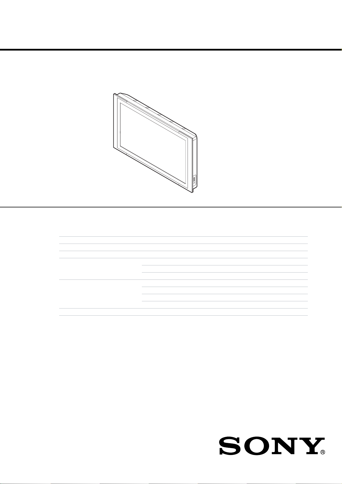
KDE-W50A10
SERVICE MANUAL
Korea Model
XS2 CHASSIS
Panel System
Display resolution
Antenna
Television System
Channel Coverage
Power Requirements
SPECIFICATIONS
Plasma Display panel
KDE-W50A10
75-ohm external terminal for VHF/UHF
NTSC
ATSC (8VSB terrestrial)
QAM on cable
Terrestrial (analog)
Cable TV (analog)
Terrestrial (digital)
Cable TV (digital)
220V, 60 Hz
1365 pixels (horizontal) × 768 pixels (vertical)
American TV Standard
ATSC compliant 8VSB
ITU-T J.83 Annex B compliant 64/256 QAM
2-69
1-125
2-69
1-135
Plasma TV
Page 2

Inputs/Outputs
HDMI IN
Video (IN)
S Video (IN)
Audio (IN)
Component Video Input
CONTROL S (IN)
CONTROL S (OUT)
Digital Audio Optical Output
(PCM/Dolby Digital)
Variable/Fixed Audio (OUT)
Sub woofer (OUT)
Screen Size (measured diagonally)
Speaker Output
CENTER SPEAKER IN
Dimensions (W × H × D)
Mass
Power Consumption
Supplied Accessories
Video
Audio
1080i, 720p, 480p, 480i
Two channel linear PCM 32, 44.1 and 48 kHz,
16, 20 and 24 bits
3 total (1 on left side panel)
3 total (1 on left side panel)
1 Vp-p, 75 ohms unbalanced, sync negative
Y: 1 Vp-p, 75 ohms unbalanced, sync negative
C: 0.286 Vp-p (Burst signal), 75 ohms
5 total (1 on left side panel)
500 mVrms (100% modulation)
Impedance: 47 kilohms
B
, PR)
2 (Y, P
1
1
1
1
1
KDE-W50A10
Y: 1.0 Vp-p, 75 ohms unbalanced, sync negative;
B
: 0.7 Vp-p, 75 ohms
P
R
: 0.7 Vp-p, 75 ohms
P
Mini jack
Mini jack
Optical rectangular (1)
More than 408 mVrms at the maximum volume
setting (Variable)
More than 408 mVrms (Fixed)
Impedance (output): 2 kilohms
Phono jack
50 inches
25 W × 2 + 50 W woofer
Max. 180 W (6 Ω), 1 kHz, Sensitivity 30 Vp-p
×
789×89 mm
KDE-W50A10
KDE-W50A10
In Use
In Standby
Remote Control (1)
1336
54.0 kg
KDE-W50A10: 430 W
0.5 W
RM-KA002
AA (R6) Batteries (2)
AC power cord (1)
AC plug holder (1)
75-ohm coaxial RF cable (1)
AC cord clamp (1)
Cleaning Cloth (1)
Operating Instructions (1)
Quick Setup Guide (1)
Warranty Card (1)
Design and specifications are subject to change without notice.
KDE-W50A10 (K) 2
Page 3

SAFETY CHECK-OUT
After correcting the original service problem, perform the
following safety checks before releasing the set to the customer:
1. Check the area of your repair for unsoldered or poorly-soldered connections. Check the entire board surface for solder
splashes and bridges.
2. Check the interboard wiring to ensure that no wires are
“pinched” or contact high-wattage resistors.
3. Check that all control knobs, shields, covers, ground straps,
and mounting hardware have been replaced. Be absolutely certain that you have replaced all the insulators.
4. Look for unauthorized replacement parts, particularly transistors, that were installed during a previous repair. Point them
out to the customer and recommend their replacement.
5. Look for parts which, though functioning, show obvious signs
of deterioration. Point them out to the customer and recommend their replacement.
6. Check the line cords for cracks and abrasion. Recommend the
replacement of any such line cord to the customer.
7. Check the antenna terminals, metal trim, “metallized” knobs,
screws, and all other exposed metal parts for AC Leakage.
Check leakage as described right.
LEAKAGE TEST
The AC leakage from any exposed metal part to earth ground and
from all exposed metal parts to any exposed metal part having a
return to chassis, must not exceed 0.5 mA (500 microamperes).
Leakage current can be measured by any one of three methods.
1. A commercial leakage tester , such as the Simpson 229 or RCA
WT -540A. Follow the manufacturers’ instructions to use these
instruments.
2. A battery-operated AC milliammeter. The Data Precision 245
digital multimeter is suitable for this job.
3. Measuring the voltage drop across a resistor by means of a
VOM or battery-operated AC voltmeter. The “limit” indication is 0.75 V, so analog meters must have an accurate lowvoltage scale. The Simpson 250 and Sanwa SH-63Trd are examples of a passive VOMs that are suitable. Nearly all battery
operated digital multimeters that have a 2 V AC range are suitable. (See Fig. A)
WARNING!!
SAFETY-RELATED COMPONENT WARNING!!
COMPONENTS IDENTIFIED BY SHADING AND MARK !
ON THE SCHEMATIC DIAGRAMS, EXPLODED VIEWS
AND IN THE PARTS LIST ARE CRITICAL FOR SAFE
OPERATION. REPLACE THESE COMPONENTS WITH
SONY PARTS WHOSE PART NUMBERS APPEAR AS
SHOWN IN THIS MANUAL OR IN SUPPLEMENTS PUBLISHED BY SONY. CIRCUIT ADJUSTMENTS THAT ARE
CRITICAL FOR SAFE OPERATION ARE IDENTIFIED IN
THIS MANUAL. FOLLOW THESE PROCEDURES WHENEVER CRITICAL COMPONENTS ARE REPLACED OR
IMPROPER OPERATION IS SUSPECTED.
AVERTISSEMENT!!
ATTENTION AUX COMPOSANTS RELATIFS À LA
SÉCURITÉ!!
LES COMPOSANTS IDENTIFIÉS PAR UNE TRAME ET
UNE MARQUE ! SONT CRITIQUES POUR LA
SÉCURITÉ. NE LES REMPLACER QUE PAR UNE
PIÈCE PORTANT LE NUMÉRO SPECIFIÉ. LES
RÉGLAGES DE CIRCUIT DONT L’IMPORTANCE EST
CRITIQUE POUR LA SÉCURITÉ DU
FONCTIONNEMENT SONT IDENTIFIÉS DANS LE
PRÉSENT MANUEL. SUIVRE CES PROCÉDURES
LORS DE CHAQUE REMPLACEMENT DE
COMPOSANTS CRITIQUES, OU LORSQU’UN MAUVAIS
FONCTIONNEMENT EST SUSPECTÉ.
To Exposed Metal
Parts on Set
0.15 µF
1.5 k
Ω
Earth Ground
AC
Voltmeter
(0.75 V)
Fig. A. Using an AC voltmeter to check AC leakage.
KDE-W50A10 (K) 3
Page 4

TABLE OF CONTENTS
1. DISASSEMBLY ............................................ 1-1
1-1. SERVICE POSITION ........................................ 1-1
1-1-1. PANELS AND CAP REMOVAL ................. 1-1
1-1-2. WOOFER BLOCK REMOVAL ................... 1-1
1-1-3. REAR COVER ASSY REMOVAL .............. 1-1
1-2. STAND, WOOFER BLOCK ASSY REMOVAL
............................................................................ 1-2
1-3. REAR COVER REMOVAL .............................. 1-2
1-4. TERMINAL BOARD AND POT COVER ASSY
REMOVAL ........................................................ 1-3
1-5. QM AND QT BOARDS REMOVAL ............... 1-3
1-6. DE3, DIC3, J1NU, J2NU AND M1U
BOARDS REMOVAL ....................................... 1-4
1-7. A1U, A2NU AND P BOARDS REMOVAL .... 1-4
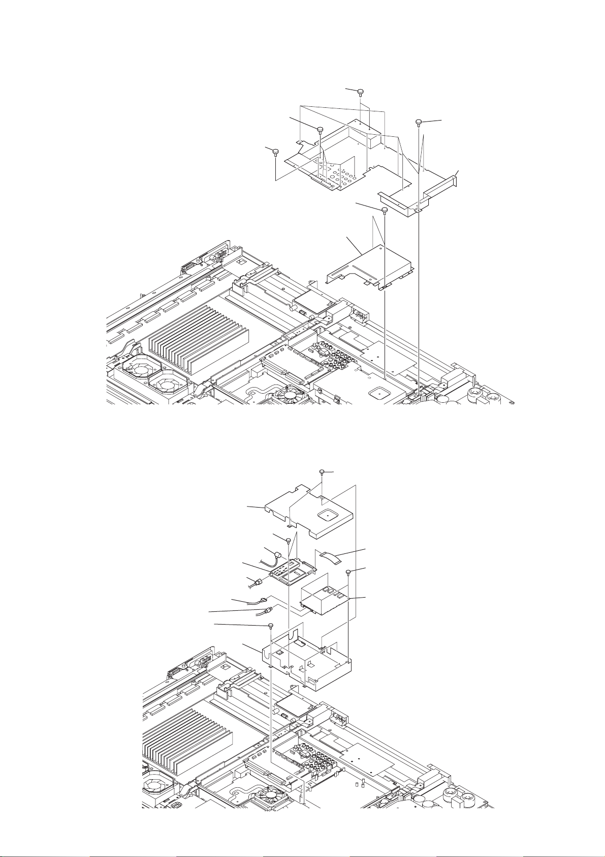
1-8. G1 AND G2N BOARDS REMOVAL .............. 1-5
1-9. F AND K BOARDS REMOVAL ...................... 1-5
1-10. H1U BOARD REMOVAL ................................ 1-6
1-11. H2 AND QH BOARDS REMOVAL ................ 1-6
1-12. PLASMA DISPLAY PANEL
ASSY REMOVAL ............................................. 1-7
1-13. H3 AND H4 BOARDS REMOVAL ................. 1-8
1-14. H5 BOARD REMOVAL ................................... 1-8
2. TROUBLESHOOTING.................................. 2-1
4-2. FRAME DIAGRAMS ........................................ 4-13
4-3. CIRCUIT BOARDS LOCATION ..................... 4-14
4-4. SCHEMATIC DIAGRAMS AND
PRINTED WIRING BOARDS........................ 4-14
(1) Schematic Diagrams of A1U Board.............. 4-15
(2) Schematic Diagrams of A2NU Board........... 4-19
(3) Schematic Diagram of F Board ..................... 4-22
(4) Schematic Diagrams of G1 Board................. 4-23
(5) Schematic Diagrams of G2N Board.............. 4-26
(6) Schematic Diagram of H1U and H2 Boards
........................................................................ 4-29
(7) Schematic Diagram of H3 and H4 Boards
........................................................................ 4-30
(8) Schematic Diagram of H5 Board .................. 4-31
(9) Schematic Diagram of QH Board.................. 4-32
4-5. SEMICONDUCTORS ....................................... 4-33
5. EXPLODED VIEWS...................................... 5-1
5-1. REAR COVER ASSY AND STAND ............... 5-2
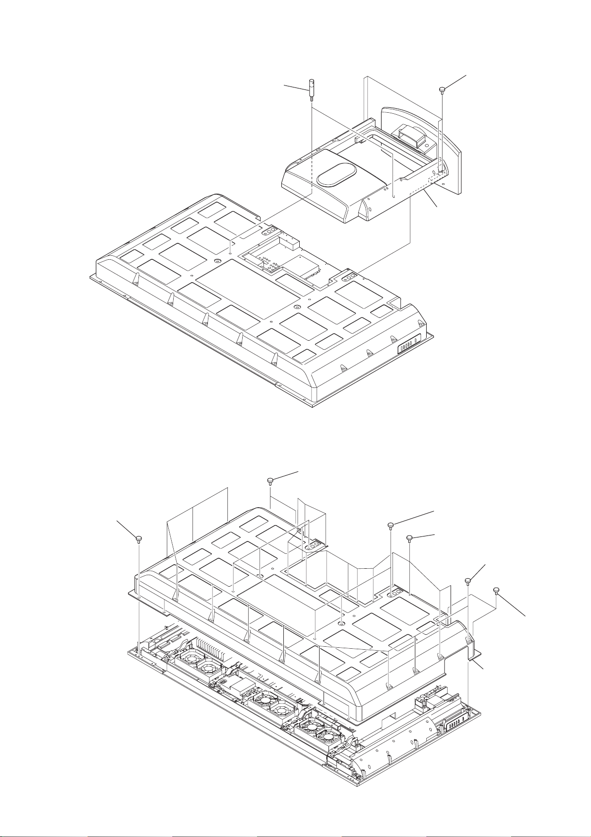
5-2. CHASSIS-1 ........................................................ 5-3
5-3. CHASSIS-2 ........................................................ 5-4
5-4. CHASSIS-3 ........................................................ 5-5
5-5. CHASSIS-4 ........................................................ 5-6
5-6. PACKING MATERIALS .................................. 5-7
3. ADJUSTMENTS ........................................... 3-1
3-1. SERVICE MODE............................................... 3-1
3-2. SERVICE MODE LIST ..................................... 3-1
4. DIAGRAMS................................................... 4-1
4-1. BLOCK DIAGRAMS ........................................ 4-1
(1) A1U AND H2 BOARDS............................... 4-1
(2) A2NU (1/2) AND J1NU BOARDS............... 4-2
(3) A2NU (2/2), H4 AND J2NU BOARDS........ 4-3
(4) DE3 BOARD ................................................. 4-4
(5) DIC3 BOARD................................................ 4-5
(6) F AND G1 BOARDS..................................... 4-6
(7) G2N BOARD................................................. 4-7
(8) K BOARD...................................................... 4-8
(9) H1U, H3, H5 AND M1U BOARDS ............. 4-9
(10) P BOARD....................................................... 4-10
(11) QH AND QM BOARDS ............................... 4-11
(12) QT BOARD ................................................... 4-12
6. ELECTRICAL PARTS LIST ........................ 6-1
KDE-W50A10 (K) 4
Page 5
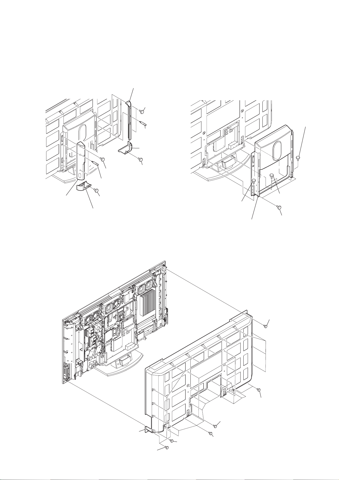
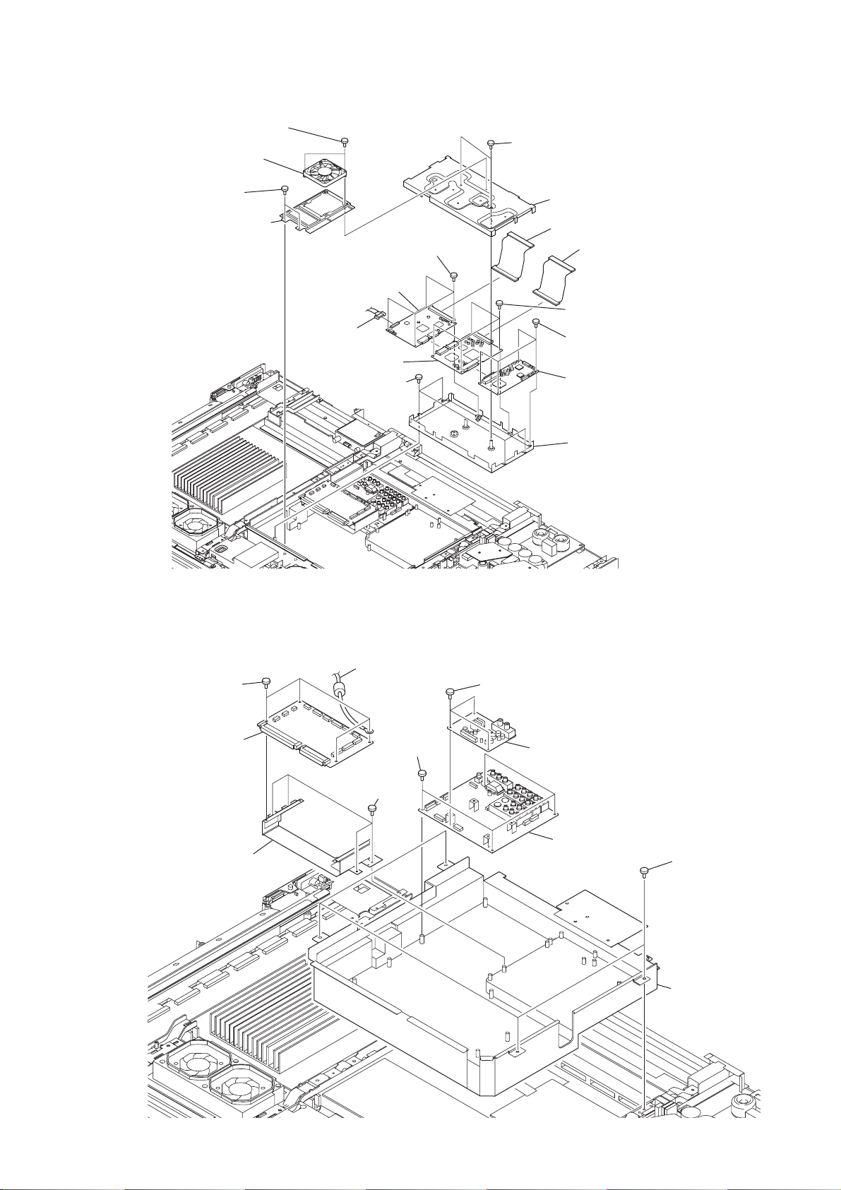
1-1. SERVICE POSITION
1-1-1. PANELS AND CAP REMOVAL
8 Ornament panel (L)
SECTION 1
DISASSEMBLY
1-1-2. WOOFER BLOCK REMOVAL
7 Two screws
(+PSW 4x8)
1 Screw
(+PSW 4x10)
6 Screw
(HOOK, M5)
0 Bottom cap (L)
9 Screw
(+BVTP 4x10)
3 Ornament panel (R)
2 Two screws
(+PSW 4x8)
1 Screw
(HOOK, M5)
4 Screw
(+BVTP 4x10)
5 Bottom cap (R)
1-1-3. REAR COVER ASSY REMOVAL
1 Screw
(+PSW 4x10)
4 Woofer block
3 Two screws
(BUTTON HEAD 6x40)
2 Two screws
(+PSW 4x10)
3 Four screws
(+PSW 4x6)
5 Rear cover assy
3 Two screws
(+PSW 4x6)
4 Twelve screws
(+BVTP 4x16)
3 Two screws
(+PSW 4x6)
1 Six screws
(+PSW 5x10)
2 Fourteen screws
(+PSW 3x6)
KDE-W50A10 (K) 1-1
Page 6
1-2. STAND AND WOOFER BLOCK ASSY REMOVAL
1 Two screws
(HOOK, (M5))
2 Four screws
(+PSW (M5))
3 Stand and woofer block assy
1-3. REAR COVER ASSY REMOVAL
4 Four screws
(+PSW 4x6)
3 Two screws
(+PSW 4x6)
1 Six screws
(+PSW 5x10)
2 Fourteen screws
(+PSW 3x6)
5 Twelve screws
(+BVTP 4x16)
3 Two screws
(+PSW 4x6)
6 Rear cover assy
KDE-W50A10 (K) 1-2
Page 7
1-4. TERMINAL BOARD AND POT COVER ASSY REMOVAL
1 Two screws
(+BVTP 4x16)
3 Five screws
(+BVTP 3x12)
4 Screw
(+PSW 3x8)
6 Two screws
(+PSW 3x6)
7 Pot cover assy (50W)
2 Seven screws
(+PSW 3x6)
5 Terminal board
1-5. QM AND QT BOARDS REMOVAL
2 Top STSC shield
6 Two screws
(+PSW 3x6)
4 RF cable
7 QT board
5 Coaxial cable with F-PLUG
8 Lead wire
connector (LVDS)
9 Cable,USB
qs Four screws
(+PSW 3x5)
qd Bottom ATSC shield
1 Two screws
(+PSW 3x6)
3 Connecter assy (FFC40P)
0 Four screws
(+PSW 3x6)
qa QM board
KDE-W50A10 (K) 1-3
Page 8
1-6. DE3, DIC3, J1NU, J2NU AND M1U BOARDS REMOVAL
1 Two screws
(+PSW 4x20)
2 DC fan
5 Two screws
(+PSW 3x6)
3 Two screws
(+PSW 3x6)
4 Fan bracket (DM)
qa M1U board
9 Lead wire
connector (LVDS)
qd DIC3 board
qh Four screws
(+PSW 3x6)
0 Four screws
(+PSW 3x5)
6 Top DM shield
7 J2NU board
8 J1NU board
qs Four screws
(+PSW 3x5)
qf Four screws
(+PSW 3x5)
qg DE3 board
qj Main DM shield
1-7. A1U, A2NU AND P BOARDS REMOVAL
6 Harness with
5 Four screws
(+PSW 3x6)
7 A2NU board
9 A2NU Bracket
connector (LVDS)
3 Four screws
(+PSW 3x6)
8 Four screws
(+PSW 3x6)
1 Three screws
(+PSW 3x6)
2 P board
4 A1U board
0 Four screws
(+PSW 3x6)
qa Center bracket
KDE-W50A10 (K) 1-4
Page 9
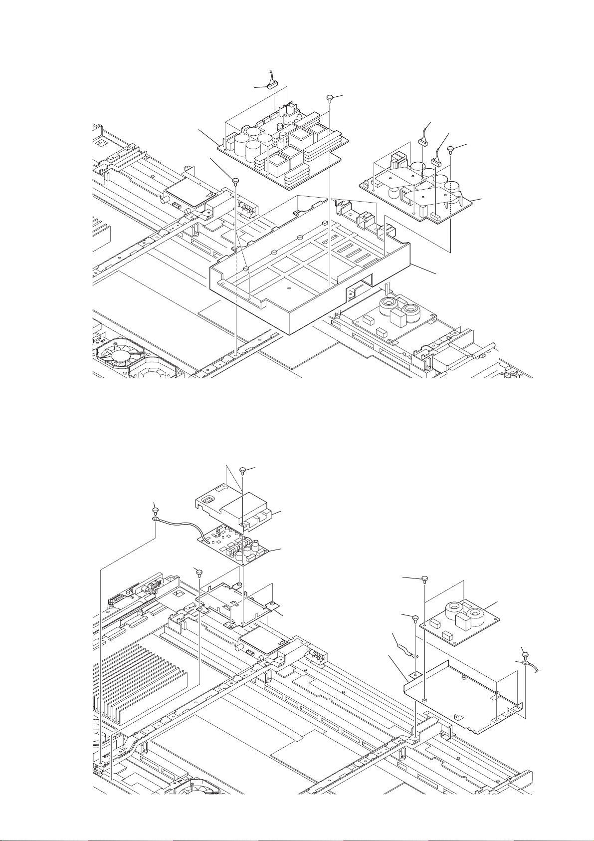
1-8. G1 AND G2N BOARDS REMOVAL
5 Connector assy (ZH6P)
7 G2N board
8 Four screws
(+PSW 4x8)
6 Four screws
(+BVTP 3x12)
1 Connector assy (VT2P)
2 Connector assy (VH5P)
3 Four screws
(+BVTP 3x12)
4 G1 board
9 G bracket assy
1-9. F AND K BOARDS REMOVAL
8 Screw
(+PSW 3x6)
0 Four screws
(+PSW 4x16)
6 Two screws
(+PSW 3x6)
7 Upper K shield
9 K board
qa Bottom K shield
1 Two screws
(+PSW 3x6)
3 Three screws
(+PSW 3x6)
Coaching clip
5 F bracket
2 F board
4 Screw
(+PSW 4x8)
Earth lead
KDE-W50A10 (K) 1-5
Page 10

1-10. H1U BOARD REMOVAL
3 Two screws
(+BVTP 3x12)
1 Two screws
(+BVTP 3x12)
2 Control panel assy
4 H1U board
1-11. H2 AND QH BOARDS REMOVAL
2 Screw
(+PSW 3x10)
1 Four screws
(+BVTP 3x12)
3 QH board
6 Screw
(+BVTP 3x12)
7 Screw
(+PSW 3x10)
4 Two screws
(+BVTP 3x12)
5 H2 board
Coaching clip
6 Screw
(+BVTP 3x12)
8 Connector panel assy
7 Screw
(+PSW 3x10)
KDE-W50A10 (K) 1-6
Page 11

1-12. PLASMA DISPLAY PANEL ASSY REMOVAL
1 Four screws
(+PSW 3x6)
7 Two screws
(+PSW 4x8)
8 Bracket fan
w; Twelve screws
(+PSW 4x8)
wa Plasma display panel assy
qh Four screws
(+P 4x16)
qj Spaker(L)
qk Four screws
(+BVTP 4x16)
ql Side plate
2 Dc fan assy
4 DC fan assy
3 Two screws
(+PSW 3x6)
5 Four screws
(+PSW 3x6)
6 DC fan assy
9 Two screws
(+BVTP 4x16)
0 Two screws
(+PSW 3x6)
qa Bottom plate
qf Four screws
(+BVTP 4x16)
qg Side plate
qs Four screws
(+P 4x16)
qd Speaker(R)
KDE-W50A10 (K) 1-7
Page 12

1-13. H3 AND H4 BOARDS REMOVAL
1 H4 board
2 H3 board
1-14. H5 BOARD REMOVAL
4 Front frame
3 Two screws
(+BVTP 4x16)
1 Two screws
(+BVTP 4x16)
2 Corner bracket
5 Screw
(+BVTP 3x12)
6 H5 board
KDE-W50A10 (K) 1-8E
Page 13

AC IN
Standby converter ON
STBY5V output
SECTION 2
TROUBLESHOOTING
POWER ON SEQUENCE for 50V
AC Relay
CN6901 pin3 “H”
G1 board
AC Relay
RY6001 ON
PFC converter
VC converter ON
32V/26V/11V/6.5V/
Thru5V out
PFC out
more than
SW 9V
out
Panel ON
CN6004_pin10 ìHî?
Yes
ON
350V ?
Yes
Yes
No
No
No
Standby mode
No Picture
VCC5V DC/DC
Converter ON
VS converter
ON
VS out
more than
150V ?
Yes
VD converter
ON
Picture appear
No
No Picture
No Picture
Standby LED
(Red) Light or
Blinking ?
Yes
Standby LED
(Red) Blinking ?
No
Power LED
(Green)
Light ?
Yes
PDP module
Priming ?
No
PDP fail
No
Yes
Panel_TEMP
Yes
F6001(AC Fuse)
Open ?
on F board
Yes
VD6001/6002 or
C6002/6004 short?
Q6206/6207/6219
2 times
Blinking?
over
No
Yes Yes
Please check VA/VS converters
Feedback circuit
CN6004 pin3
(AC_RLY) Low ?
G2 board
around micro fail
on M board
Power Supply Trouble shouting
No
R6102 Open?
on G1 board
Yes
IC6101
(Stby IC) Fail
3 times
Blinking ?
+B_OVP
VS or VA OVP
NoNo
Yes Yes
4 times
Blinking ?
FAN error
Check each FAN
RY6001
(AC Relay)
ON ?
PFC circuit fail
No
Yes Yes Yes Yes Yes
Standby Rectifier Diode
Check Secondary circuit
of Standby5V line.
6 times
Blinking ?
Low B error
TV micro P.S
No
Check each DC/DC
Check A2NU or
A2FU DD converter
Standby 5V line
converter out
OK?
Check
7 times
Blinking ?
Audio Prot
Check Audio
Amplifier
Check Signal
Processes circuit
NoNoNoNo No
9 times
Blinking ?
Panel error
Check PDP
Look at VA/VS Converter
trouble shooting. after page
11 times
Blinking ?
Convt_error
P.S fail
KDE-W50A10 (K) 2-1
Page 14
PFC converter fail
on G1 board
(Vout<350V)
PFC converter trouble shooting
PFC out
CN6017 pin5
Vout<10V?
At 120V input
Yes
Please check F6001
R6005/6006/6007
Q6206/6207/6219
No No
PFC out
CN6017 pin5
200V<Vout<350V ?
Yes
Re Adjust for RV6201
Check RV6201,IC6202
No
IC6202 pin15
12V ?
Yes
IC6202 pin16
pulse waveform
appear?
Yes
Check R6233
Q6203/6205
No
Check IC6202
CN6017 pin2
More than 15V?
Yes
When turn ON
IC6203 pin14
“H”?
Yes
PFC OVP operate
Check R6249
~RV6201
No
No
Standby
Floating 18V fail
Check IC6201
VC converter fail
on G2 board
R6302 Open?
Q6301,Q6302
Fail *1
*
1 If Q6301 and Q6302 fail
Must be change D6306 and D6307
Pin12
No
3V
Shut Down
When turn on
IC6301 pin3
saw waveform appear?
When turn on
IC6301 pin20
pulse waveform appear?
IC6301 pin12
more than 3V ?
IC6301 OCP operate
VC Secondary side
short circuit.
No
YesYes
Yes
No
Yes
VC converter trouble shooting
Yes
NoNo
KDE-W50A10 (K) 2-2
Check Standby
Power Supply
Check R6301,
IC6301 pin15
more than 15V ?
Yes
IC6301 pin1
more than 1.4V ?
IC6301 or
PH6401,IC6405 fail.
NoNo
Yes
CN6017 pin2
more than 15V?
IC6301
Fail
R6316
Page 15

VA converter fail
on G2 board
VD converter trouble shooting (NPD)
R6503 Open?
Q6503,Q6504
Fail *1
*1 If Q6503 and Q6504 fail
Must be change D6506 and D6507
Pin12
No
3V
Shut Down
When turn on
IC6501 pin3
saw waveform appear ?
YesYes
When turn on
IC6501 pin20
pulse waveform appear ?
Yes
IC6501 pin12
more than 3V ?
Yes
IC6501 OCP operate
VA Secondary side
short circuit
No
more than 15V ?
more than 1.4V ?
No
PH6601,IC6601 fail
IC6501 pin15
Yes
IC6501 pin1
Yes
IC6501 or
NoNo
C6315
more than 15V?
Yes
Q6918&Q6909
C “H”?
No
PFC out
more than 350V ?
Yes
VCC5V
OK ?
No
Check IC6408,
Q6406
NoNo
Yes
No
Yes
VC converter
or Vccline fail
Check R6502
Check
PH6905,Q6502
Check PFC or
re Adjustment
PFC Voltage
Check
around Q6926,
IC6905
VS converter fail
on G2 board
R6703 Open?
Q6705,Q6706
Fail
*1 If Q6705 and Q6706 fail
Must be change D6707 and D6708
No
When turn on
IC6701 3pin
saw waveform appear?
YesYes
When turn on
IC6701 20pin
pulse waveform appear?
Yes
IC6701 12pin
more than 3V ?
Yes
IC6701 OCP operate
VS Secondary side
short circuit
VS converter trouble shooting
No
more than 15V ?
more than 1.4V ?
No
PH6801,IC6801 fail.
IC6701 15pin
Yes
IC6701 1pin
Yes
IC6701 or
NoNo
more than 350V ?
C6315
more than 15V?
Q6909 C
“H” ?
PFC out
VCC5V
OK ?
NoNo
Yes
Yes
No
No
Yes
Yes
No
VC converter
or Vcc line fail
Check R6702
Check
PH6903,Q6702
Check PFC or
re Adjustment
PFC Voltage
Check
near Q6926,
IC6905
Check IC6408,
Q6406
KDE-W50A10 (K) 2-3
Page 16

No Picture
A1U Trouble shooting (Video)
Panel is
priming?
YES
No picture for all
inputs?
NO
Twin view is
O.K?
YES
Sub Picture is
O.K
YES
5 pin of CN306
has video signal?
YES
M1U/DIC3/DE3
trouble
NO
YES
NO
NO
NO
Not A1U trouble
Check no picture
input
M1U/DIC3/DE3
trouble
20 pin of CN001
has video signal
for sub picture?
YES
NO
RF
V1, 2, 3
V4, 5
V6
Check DM Block
Check input path
Check IC404,
Q410 ~ Q412
Check P Board
Check circuit
around IC303
No Sound
Red flashing
7 times ?
YES
Connector for K board is O.K?
To A2, DE3, G2N
YES
Power source for K board is
O.K?
AU25V on CN2062
5V, SUB11V on CN2600
YES
K or DE3 trouble
A1U Trouble shooting (Audio)
NO
NO
NO
Check
connector
Power module
might have
trouble
No sound for
all inputs?
NO
Audio is
O.K?
YES
SPDIF signal is O.K?
(check CN2002 6 pin of
A2N
YES
K trouble
NO
YES
NO
Check input path
from each input to
IC507
TP503, 504
have audio
signal?
YES
Check circuit
around IC552
NO
Check circuit
around IC507
KDE-W50A10 (K) 2-4
Page 17

No Picture
A2NU Tr oubl e Shooting
NO
NO
M1U trouble
Red flashing
6 times
?
YES
JL2016 and
JL2017 level are
High?
YES
JL2002 outputs
5V?
YES
NO
NO
PS2001 is opened or
IC 2001 is broken.
Otherwise check
JL2019 is 11V or not.
Green flashing
Continuously
(90 sec)
?
YES
JL2001 outputs
10.2V?
YES
JL2011 outputs 3.3V?
JL2003 outputs 2.5V?
YES
Not A2NU trouble
NO
NO
NO
Not A2NU trouble
JL2019 outputs
10.2V?
YES
Q2008 is broken
JL2018 outputs
6.5V?
PS2001 is opened or
IC 2001 is broken
NO
NO
Power module
might have trouble
No Set Power
Power LED is
Green?
Green LED is
flashing?
Check connection
M1U to DIC3.
Check connection
DIC3 to DE3.
Check connection
M1U to DM
YES
YES
M1U Tr oub le Shooting -1
NO
NO
STBY5V(CN7004,
A1,A2, B1) is 5V?
YES
Check connection A2NU
Check Power module and
A2NU
YES
CN7004(120pinBtoB)
B33, A34 are High?
NO
NO
Replace M1U
KDE-W50A10 (K) 2-5
Page 18

M1U Tr oub le Shooting -2
These symptom might be related M1U board as below.
-Strange Menu OSD or Lack of upper side in Media Viewer mode
-Check connector CN7650 (LVDS Connector to QM)
-Check connector CN7552 and CN7553(B to B connector to DIC3)
-IC7650 (LVDS Receiver) might be broken or not operate correctly
-No Sub Picture
-IC7701 (CCPX) or path to IC7701 might be broken or not operate
correctly
-Closed Caption Decode error in good signal condition
-IC7002 (TV Micro) or path to IC7701 might be broken or not
operate correctly
DIC3 Power Trouble Shooting -1
Symptom
No Video and Audio
No Menu OSD
But video signal is coming DIC3 board
Power provided to DIC3
board correctly?
YES
Power generated inside
DIC3 board correctly?
NO
YES
YES
I2C signal from M1U is
O.K? (CN4003, 41/42pin)
NO
Remove CN4003.
M1U outputs I2C signal
correctly?
YES
DIC3 outputs I2C
signal? (JL4000 : SDA,
JL4001 : SCL)
YES
DIC3 outputs H/V sync and CLK?
CLK (CN4204 A4) :
FHP 40MHz ,NPD 80MHz
Hsync (DE3, R5159) : 33.75KHz
Vsync (DE3, R4254) : 60Hz
NO
NO
Replace DIC3
Check other moduleReplace DIC3
KDE-W50A10 (K) 2-6
Page 19
DIC3 Power T roubl e Shooting -2
Symptom
Some input source or picture mode has
no picture. Menu OSD and Audio are
O.K
Direct Mode OFF/ON
makes picture appear?
YES
No Picture or
Abnormal Picture
NO
Changing DRC mode
NO
makes picture appear?
YES
Replace DIC3
DE3 T rouble s hoot for NPD(50”)
Check other module
TV Micro
Service
Mode is OK?
Yes
DE Service
45 TEST
0 TESTON
0→1 OK?
Yes
CN5101 or
IC5302 or
DIC3
CHECK
No
No
Power
Supply for
Panel is OK?
Yes
3.3V and
1.8V is OK?
Yes
IC3501
(VORTEX)
Circuit CHECK
No
No
IC5207 or IC5210
or SUB6.5V or
SET_ON_DE
CHECK
CN5203
PANEL_ON
is High
Level?
Yes
NPD PANEL or
Power Supply for
PANEL
CHECK
No
IC5202
(DE Micro)
Circuit CHECK
KDE-W50A10 (K) 2-7
Page 20

P Symptom & A ction
Replace [P] board when those symptom has occurred as below.
-No Picture / No Sound
PS9500 might be open.
IC9505 might be broken.
-No Sound
IC9504 might be broken or not operate correctly.
-Shaking Picture
Possible Claims about connectivity
-Aspect Ratio
-Greenish Picture / Pinkish Picture
-Snow Picture
-No Picture / No Sound
-No Sound
→
Those case are not [P] boar d broken.Those claims is the cause of combination
between TV and Source Device (DVD etc.).
K Tro u b le Shooting -1
•Symptom 1:No or irregular sounds from the L/R channel (but not from the Woofer Channel).
(To do) Check the input signals to and output signals from the IC2604.
(Your results) There are IIS input signals to the IC, but no PWM or irregular output signals
from the IC.
(Cause) The IC2604 itself might have been sub-standard, or broken.
•Symptom 2: No or irregular sounds from the Woofer channel (but not from the L/R channel)
(To do) Check the input signals to and output signals from the IC2607.
(Your results) There are IIS input signals to the IC, but no PWM or irregular output signals from
the IC.
(Cause) The IC2607 itself might have been sub-standard, or broken.
•Symptom 3: No sounds from either Lch, Rch, or Wch (Only one of three).
(To do) Check the IC2605 (Lch), IC2606 (Rch) and IC2608 (Wch).
(Your results) There are IIS input signals to one of the each, but no PWM or irregular output
signals from one of the each.
(Cause) One of the IC2605 (Lch), IC2606 (Rch) or IC2608 (Wch) might have been sub-standard,
or broken
KDE-W50A10 (K) 2-8
Page 21

K Tro u b le Shooting -2
Symptom 4: No sounds from L, R, and Wch at all
(To do) Check the AMP_RST port of the IC2605 (Lch), IC2606 (Rch) and IC2608 (Wch).
(Your results) The AMP_RST port is utputting “L”.
(Cause) Microcontroller port (AMP_RST) error or IC2602 and/or IC 2614 might have been
sub-standard or broken
(To do) Check the M_RST port of the LC89056 (IC2600) and CXD9788R (IC2604, IC2607)
(Your results) The M_RST port is outputting “L”
(Cause) Microcontroller port (M_RST) error or IC2609 might have been sub-standard or
broken
(To do) Check the input and output voltage of the IC6103<3.3V> an d IC6101<12V>
(Your results) There are voltages supplied to the IC6103<3.3V> or IC6101<12V> but no
output voltage from ei ther/both ICs
(Cause) Regulators (IC6103<3.3V> or IC6101<12V>) might have been sub-standard or
broken.
(To do) Check the input signals to or output signals from the CXD9835TN (IC2603)
(Your results) There are input IIS signals to the IC, but no output signals from the IC
(Cause) IC2603 might have been sub-standard or broken
(To do) Check the input signals to or output signals from the LC89056 (IC2600)
(Your results) There are input SPDIF signals to the IC, but no output signals from the IC
(Cause) IC2600 might have been sub-standard or broken.
K Tro u b le Shooting -3
•Symptom 5: Different sounds or irregular sound from L,R, or W ch
(Check) Check the input signals to or output signals from the CXD9835TN (IC2603)
(Result) There are input IIS signals present, but no or irregular output signals from the IC
(Cause) IC2603 might have been sub-standard or broken
•Symptom 6: Interrupted or noisy sounds from the L, R, or/and W ch
(Check) Check the error port (JL 2616) of the LC89056 (IC2600)
(Result) Outputting “H”
(Cause) SPDIF error .
SPDIF transmitter might have been sub-standard or broken
or LC89056 (IC2600) might have been sub-standard or broken
KDE-W50A10 (K) 2-9
Page 22

Trouble shooting
related with Digital Module
Connection failure
• Set no power
– CN7300 connection or cable damage.
• No DTV and No Memorystick. But NTSC is OK.
– CN7309 connection or cable damage. (DA4, AX1X, LA3, Plasma)
No DTV. But Memorystick and NTSC is OK.
– 40Pin FFC connection or cable damage.
• No DTV and No NTSC. But Memorystick is OK.
– RF cable (F-F) or ANT-SW 5pin wire connection or cable damage.
• No NTSC. But DTV and Memorystick is OK.
– CN7901 is connection or cable damage.
• No menu OSD. But Memorystick mode is OK.
– CN7304 connection or cable damage. (LA3, SXRD, Plasma)
• Memorystick is not detected by insertion.
– USB connection or cable damage.
• Only no Digital cable video/audio. ATSC is OK.
– RF cable (P-P) or 80Pin FFC connection or cable damage.
KDE-W50A10 (K) 2-10
Page 23

Key Component/Circuit failure
)
• ATi chip failure
– Reboot (intermittent video)
– Distorted graphics (block noise error on Menu or Memorystick)
• Power supply failure (QM or Set power)
– No power (cannot see heart beat LED from jig CN. But can see one of QT
LED.)
• NTSC demodulator failure.
– No Audio. Distorted audio. No NTSC video.
• Tuner (Insi de of Front End) failure.
– No NTSC, No ATSC, No D-Cable.
• Digital demodulator failure.
– No DTV (ANT, Cable)
– May not boot the system.
• i.LINK(80/40pin BtoB CN or i.CES(BGA chip on QI or QFP IC) failure.
– No i.LINK (D-VHS, DV
KDE-W50A10 (K) 2-11E
Page 24
SECTION 3
ADJUSTMENTS
3-1. SERVICE MODE
1. How to Enter Service Mode
1) Turn on the main power switch to place this set in standby
mode. (The LED will light red.)
2) Press the buttons on the commander as follows to enter
service mode.
5
(VOLUME +)(DIGIT 5)(DISPLAY) (POWER)
2. Press the JUMP key on the commander three times.
3. How to Adjust
“ 29 MAIN_WB”
Category name.
(Can be changed with the 2 and 5 keys on the commander.)
5 GAINR 512
Data Can be changed with the 3 and
6 keys on the commander.
Item Name Can be changed with the 1 and
Item No. 4 keys on the commander.
4. After the adjustment is completed, save the data using the
MUTE and ENTER keys.
Enter the
“Service mode”
3-2. SERVICE MODE LIST
CATEGORY
MAIN_WB
ITEM
NO.
5
6
7
Name
GAINR
GAING
GAINB
DATA
512
512
512
KDE-W50A10 (K) 3-1E
Page 25
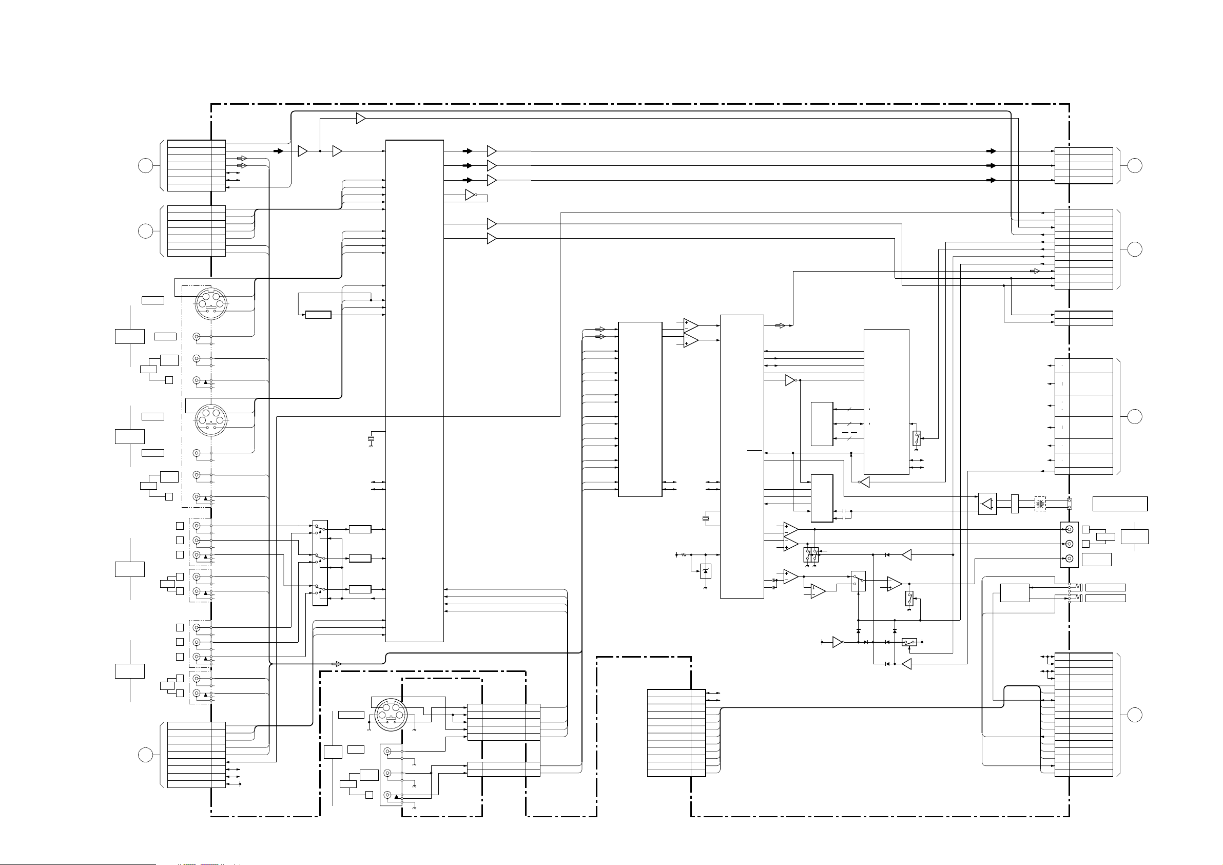
4-1. BLOCK DIAGRAMS
3P
2P
3P
J310
J309
J300
J302
J304
R2
L2
V2
SW2
R1
L1
V1
SW1
43
21
43
21
R
R
HD/DVD IN
4
P
R
B
P
Y
R
L
AUDIO
AUDIO
L
R
Y
P
B
R
P
5
HD/DVD IN
S VIDEO
VIDEO IN
3
VIDEO
VIDEO
S VIDEO
1
VIDEO IN
CN005
1
2
4
6
8
9
10
AFTM
TU1V
TU1R
TU1L
SCLK
SDAT
AGC MUTE
CN006
A2
A4
A6
B1
B2
B4
B6
Pr
Pb
Y
H
V
R
L
SCL
SDA
R
L
Q317 Q315
ATSC R
ATSC L
V3_L
V3_R
V1_R
V1_L
IC404
CN002
13
11
9
7
6
4
3
2
1
Y
PB
PR
L
R
RESET
SDA
SCL
9V
SDA
SCL
SW9V
IN1_CV
IN1O_Y
IN10_CB
IN10_CR
IN10_L1/H
IN10_L2/V
IN6_CV
IN6_Y
IN6_C
IN6_S
IN5_CV
IN5_Y
IN5_C
IN5_S
EXT_CLK/XTAL
SCL
SDA
IN9_CR
IN9_CB
IN9_Y
DC_OUT
IN8_Y
IN8_CB
IN8_CR
79
40
41
42
43
44
19
18
17
16
11
12
13
51
SYNC SEP
Q302-304
X302
4MHz
SDA
SCL
76
77
COMP1_L
COMP1_R
COMP2_R
COMP2_L
8
9
14
11
1
16
6
5
3
35
34
33
74
26
27
28
HDMI_L
HDMI_R
VIDEO SW
IC303
CV/YOUT1
C/CBOUT1
CROUT1
SEL_OUT1
SYNC_IN1
CV/YOUT2
C/CBOUT2
Q316
58
59
Q314
60
Q313
67
Q320
68
Q321
34
1
2
6P
J1101
L
R
V
J1102
VIDEO
L
R
AUDIO
VIDEO2
INPUT
S VIDEO
CN1102 CN004
2
4
6
8
10
V2_SW
V2 S2
V2 C
V2 Y
V2 V
4
2
CN1104
V2 L
V2 R
1
2
4
6
8
10
12
IN4_CV
IN4_Y
IN4_C
IN4_S
7
8
9
6
H2
IN8_L
IN8_R
IN10_L
IN10_R
IN2_L
IN2_R
IN1_L
IN1_R
IN4_L
IN4_R
IN5_L
IN5_R
IN6_L
IN6_R
IN7_L
IN7_R
LOUT1
ROUT1
SCL
SDA
22
23
28
29
4
5
1
2
10
11
13
14
16
17
L
R
ATSC_L
ATSC_R
V3_L
V3_R
V1_L
V1_R
COMP1_L
COMP1_R
COMP2_L
COMP2_R
HDMI_L
HDMI_R
V2_L
V2_R
IC507
AUDIO SW
SCL
SDA
31
32
3
2
6
5
1
7
39
37
56
57
SC1_IN_L
SC1_IN_R
SPDIF
_OUT
I2S_DEL_IN
I2S_DEL_OUT
I2S_DEL_CS
DVSUP
AUDIO_CLOCK
_OUT
IC526
AUDIO PROCESSOR
Q318
IC512
8
9
10
11
74
24
SRAM
IC524
I2C DAIN1
I2C_WS
I2C_CL
IC521
ADC
4
5
7
11
12
10
9
IC504
5
6
2
3
37
36
7
1
Q503Q504
34 2
3
33
IC502
7
5
6
IC501
IC501
1
6
7
3
2
1
1
IC510
17
A0-A16
IO0-I07
8
WE/OE
2
CN306
5
1
3
MAIN_Y/CV
MAIN_C/CB
MAIN_CR
CN001
1
2
4
6
7
8
9
11
15
18
19
HDMI RST
AFT MAIN
TU_H_MAIN
AGC_ATT
AD_RST
AD_MUTE
LINE MUTE
SP MUTE
SPDIF
SUB_C
SUB_Y
CN010
1
2
5
7
9
12
15
18
24
25
27
28
30
STBY5V
SW9V
D5V
A5V
3.3V
11V
AC_RLY
L
R
SUBWOOFER
AUDIO
J307
DELAY IC
B
TO
A2NU(1/2)BOARD
CN8209
CN8205
A2NU(2/2) BOARD
TO
C
D
TO
A2NU(1/2)BOARD
CN8206
59
13
8
7
11
A16
A0
IO0
IO7
RST
MUTE
6
RESET
DIGITAL
_CONTROL_OUT_0
IC522
IC523
13
2
5
IC500
MATREX
T501
STBY5V
SW9V
D5V
A5V
3.3V
SUB11V
Q502
STBY5V
Q515
Q514
Q512
Q508
5
1821
78
Q306-Q312
IN-OUT
CTRL
CN011
3
4
7
8
9
13
14
15
17
19
21
22
23
25
27
28
29
I2C_SCL
I2C_SCL
I2C_SDA
I2C_SDA
B_INT
USBDPLS
SIRCS
USBDMNS
USBCONNECT
JIG_VBUS
JIG_UDP
UARTRXDP
JIG_UDM
PAN_UDM
PAN_UDP
USER_TXD
PAN_VBUS
SCL
SDA
CN304
1
2
3
5
6
7
8
9
10
11
12
13
CLK_S
DAT_S
B_INT
TVM_UDP
TVM_UDM
TVM_VBUS
IFP_UDP
IFP_UDM
IFP_VBUS
PAN_UDP
PAN_UDM
PAN_VBUS
SDA
SCL
CONTROL S IN
CONTROL S OUT
J303
3
2
SDA
SCL
SDA
SCL
7218.432MHz
X501
71
XTAL_OUT
XTAL_IN
CN9504
P BOARD
TO
A
Q305
AUDIO R
AUDIO L
VIDEO
Y
B-Y
R-Y
AUDIO L
AUDIO R
AUDIO L/R
AUDIO L/R
AUDIO L/R
V2 L
V2 R
AUDIO PROCESSOR,INPUT TERMINAL)
R-Y
B-Y
Y
J305
CENTER SPEAKER IN
180W(6 )MAX
J301
CN8207
A2NU(2/2)BOARD
TO
E
Q510
1
2
14
55
56
12SUB_Y
SUB_C
CN301
AGC1
AFT1
11
(VAR/FIX)
AUDI0 IN
OUT(VAR)
U2_TX
MAIN_LOG
MAIN_LOG
U2_TX
IISM_OUT
IISM_IN
BIT_CLK
LR_CLK
FCLK
SCL
SDA
SCL
SDA
Q509
POL
CENT
Q505
D5V
(VIDEO SW,AUDIO SW,
A1U
SC1_OUT_L
SC1_OUT_R
SC2_OUT_L
SC2_OUT_R
SW9V
IC514
AHVSUP
1
3
2
19
20
SUB_Y/CB/Y
SUB_C/CB
Y
CB
CR
HS
VS
V3_SSW
V3_C
V3_Y
V3_V
V1_SSW
V1_C
V1 V
V1_V
7
BUFFER
BUFFER
BUFFER
Q410
Q411
Q412
12
2
Y
PB
PR
PR
PB
Y
(MONO)
V2_C
V2_Y
V2_V
V2_SSW
V2_SSW
V2_C
V2_Y
V2_V
(MONO)
AUDIO
R
L
L
R
AUDIO
(MONO)
V1_V
V1_SSW
V1_C
V1_Y
V3_Y
V3_C
V3_SSW
V3_V
CR
CB
Y
HS
VS
AGC1
AFT1
TO
QT BOARD
CN7901
CN7309
QM BOARD
TO
39
N
O
(1) A1U AND H2 BOARDS
SECTION 4
DIAGRAMS
KDE-W50A10 (K) 4-1
Page 26
(2) A2NU (1/2) AND J1NU BOARDS
B
TO
A1U BOARD
CN306
H
TO
G2N BOARD
CN6004
G
TO
G2N BOARD
CN6008
F
TO
G2N BOARD
CN6009
CN8209
MAIN-Y/CV
MAIN-CR
MAIN-C/CB
CN2005
AC_RLY
P_SW
STBY5V
+B_OVP
PS_PROT
POW_CTL
PANEL_ON
FAN_ERR
FAN_DRV
THRMO_G
CN2001
SUB6.5V
SUB11V
CN2004
ATSC5V
SW9V
Q2015-2018
Y
1
R-Y
3
5
3
4
6
7
8
9
10
11
12
13
3
4
8
10
3
5
6
B-Y
STBY5V
ATSC5V
SW9V
BUFFER
TO 2/2
5
SUB6.5V
SUB11V
7
6
TO 2/2
TO 2/2
8
TO 2/2
Q2008
Q2009
Q2001
Q2002
TO 2/2
9
IC2001
DC-DC CONV.
OUT2
OUT1
7
DTC2
19
STB
IC2002
DC-DC CONV.
OUT1
19
OUT2
STB
IC2004
1
9V
REG
TO 2/2
3
TO 2/2
2
IFT_BINT
11
1
SET_ON
TO 2/2
TO 2/2
Q2004
Q2003
9
11
Q2014
Q2006
11
9
3
ATSC9V
ATSC11V
D2011
2.5V
D2016
D2013
D2014
A2NU(1/2)
(POWER SUPPLY)
B-Y
Y
R-Y
SCL_1
SDA_1
SW2.5V
SW3.3V
SW5V
SUB6.5V
STBY5V
SW9V
11V
CN8203
A1,A7
I_MAIN_C
I_MAIN_CV
A3
I_MAIN_R
A5
I_MAIN_G
A9
I_USBCONNECT
A14
I_USBDMNS
A15
A17
I_USBDPLS
A19
I_UAETTXD1
A21
I_UARTRXD1
B2
B5
SET_ON
B6
B7
B8
B20
I_UARTTXDP
B22
I_UARTRXDP
A24
B24
SW2.5V
A25
B25
A27
B27
SW3.3V
A28
B28
A30
B30
A33
B33
SUB6.5V
A34
B34
A31
SYSTEM RST SYSTEM RST
B_INT
SCL_1
D_OVP
SDA_1
SW5V
A1,A7
A3
A5
A9
A14
A15
A17
A19
A21
B2
B5
B6
B7
B8
B20
B22
A24
B24
A25
B25
A27
B27
A28
B28
A30
B30
A33
B33
A34
B34
A31
CN8403CN8404
J1NU
CN8206
1
STBY5V
2
5
SW9V
7
9
D5V
12
15
A5V
18
24
3.3V
25
27
11V
28
30
AC_RLY
D
TO
A1U BOARD
CN010
A1,A7
A3
A5
A9
I_USBCONNECT
A14
A15
A17
A19
A21
B2
B5
B6
B7
B8
B20
B22
A24
B24
A25
B25
A27
B27
A28
B28
A30
B30
A33
B33
A34
B34
A31
I_MAIN_C
I_MAIN_CV
I_MAIN_R
I_MAIN_G
I_USBDMNS
I_USBDPLS
I_UAETTXD1
I_UARTRXD1
B_INT
SET_ON
SCL_1
D_OVP
SDA_1
I_UARTTXDP
I_UARTRXDP
SW2.5V
SW3.3V
SW5V
SUB6.5V
I
TO
DIC3 BOARD
CN4000
KDE-W50A10 (K) 4-2
Page 27

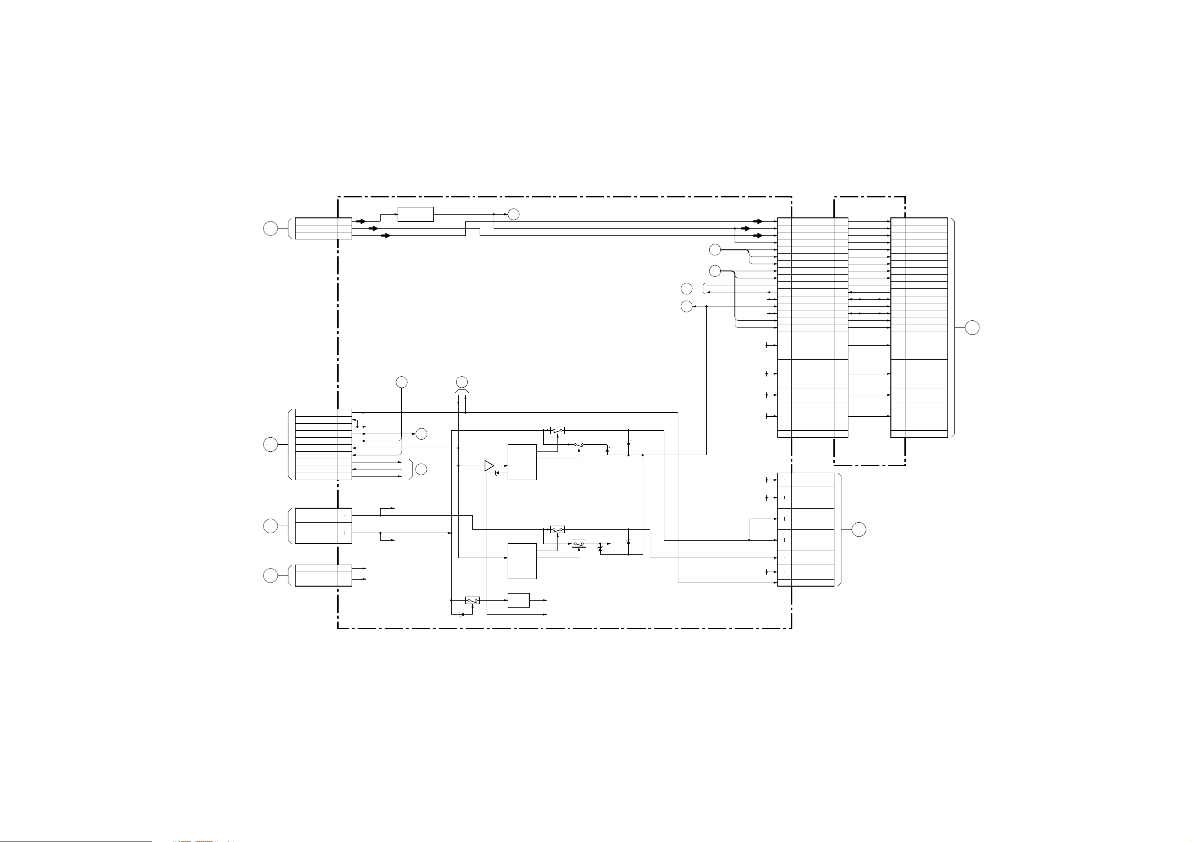
(3) A2NU (2/2), H4 AND J2NU BOARDS
M
TO
QM BOARD
CN7300
C
TO
A1U BOARD
CN001
J
TO
K BOARD
CN2600
E
TO
A1U BOARD
CN011
K
TO
DE3 BOARD
CN5203
Y
TO
QT BOARD
CN7902
CN8208
RXD
TXD
RESET
5V
9V
CN8205
HDMI RST
AFT MAIN
TU-H-MAIN
AGC ATT
AD RST
AD MUTE
LINE MUTE
SP MUTE
WOOFER MUTE
SPDIF
SUC C
SUB Y
CN2002
SW5V
SUB11V
SPDIF-
CN8207
I2C SCL
I2C SDA
B INT
AC DET(NC)
USBDPLS
SIRCS
USBDMNS
USBCONNECT
JIG VBUS
UART TRXD1
JIG UDP
UART TRXDP
JIG UDM
UART TXD1
PAN UDM
UART TXDP
PAN UDP
USER TXD
PAN VBUS
USESR RXD
CN8201
SUB6.5V
SYS RESET
THERMO G
FAN ERROR
FAN DRV
PANEL ON
PS PROT
LOGO
D OVP
PAN UDP
SET-ON DE
PAN UDM
PAN VBUS
CN8210
A1,A2
B1
A3.A4
B8
B9
A10
B10
A11
B11
A12
B12
A13
B13
A14
B14
A15
A16
B15,B16
B17,B18
A19
A21
A23
B25
B26
B27
B28
B29
A30
B30
B31
B32
B33
A34
B34
A35
B36
A37
B37
B38
B39
B40
A41
B41
B42
B44
A45
B45
A46
B46
A47
A48
A49
A50
B50
CN8401
STBY5V
D5V
+B OVP
AFT_MAIN
FMONO
AGC_ATT
I_SAP
O_SAP
AFT_SUB
FAN_POW_SW
TU_H_MAIN
FAN_SPEED
TU_H_SUB
FAN_EROR
AD_RST
AD_MUTE
ATSC5V
SW3.3V
CVY_MAIN
SUB_Y
SUB_C
ATSC_RXD
ATSC_TXD
ATSC_RST
HDMI_RST
LINE_MUTE
SP_MUTE
WOOFER_MUTE
ANT_S
ANT_M
POW_CLT
AC_RLY
SET_ON
D_OVP
SIRCS
SYSTEM_RST
JIG_UDM
JIG_UDP
USER_RXD
USER_TXD
VBUS
I2C_SDA
12C_SCL
B_INT
I2C_SW
ROM_SDA
ROM_SCL
DDC_WE
IFP_BINT
SDA_1
SCL_1
DE_RST
AC_DET
L
TO
M1U BOARD
CN7004
MS1
MS2
5V
9V
CN8402CN8204
A1,A2
B1
A3,A4
B8
B9
A10
B10
A11
B11
A12
B12
A13
B13
A14
B14
A15
A16
B15,B16
B17,B18
A19
A21
A23
B25
B26
B27
B28
B29
A30
B30
B31
B32
B33
A34
B34
A35
B36
A37
B37
B38
B39
B40
A41
B41
B42
B44
A45
B45
A46
B46
A47
A48
A49
A50
B50
J2NU
1
2
3
5
ATSC5V
9
ATSC9V
10
1
2
4
6
5
8
9
11
13
15
18
20
1
3
6
3
7
9
10
13
14
15
17
19
20
21
22
23
24
25
26
27
28
29
30
3
6
7
8
9
10
11
12
13
14
15
16
17
18
2ATSC A9V
AUDIOL/R
D5V
11V
I2C-SCL
I2C-SDA
6.5V
ATSC A9V
Q2005
A5V
STBY5V
3
2
TO1/2
TO1/2
6
TO1/2
5
CN2003
1
TO1/2
THRU5V
LOGO
TO1/2
FAN DRIVE
111
CN1501
1
22
TO1/2
6
D1501,1503,1505
D1507,1509,1511
D1513
Q1501-15073
TO1/2
SET_ON
Q2010
TO1/2
8
11
9
TO1/2
7
IFT_BINT
ATSC5V
ANTM
ANTS
Q2012
STBY5V
ATSC5V
SW3.3V
ISC SDA
I2C-SCL
Q2013
D5V
SDA-1
SCL-1
5V
9V
A1,A2
STBY5V
B1
A3,A4
D5V
B6 B6 B6
+B OVP
B8
AFT_MAIN
B9
FMONO(NC)
A10
AGC_ATT
I_SAP(NC)
B10
A11
O_SAP(NC)
AFT_SUB(NC)
B11
FAN_POW_SW(NC)
A12
TU_H_MAIN(NC)
B12
FAN_SPEED(NC)
A13
TU_H_SUB
B13
FAN_EROR
A14
AD_RST
B14
AD_MUTE(NC)
A15
ATSC5V
A16
B15,B16
SW3.3V
B17,B18
A19
CVY_MAIN
A21
SUB_Y
A23
SUB_C
B25
ATSC_RXD
B26
ATSC_TXD
B27
ATSC_RST
HDMI_RST
B28
B29
LINE_MUTE
A30
SP_MUTE
B30
WOOFER_MUTE
B31
ANT_S
B32
ANT_M
B33
POW_CLT
A34
AC_RLY
B34
SET_ON
A35
D_OVP
B36
SIRCS
A37
SYSTEM_RST
B37
JIG_UDM
B38
JIG_UDP
B39
USER_RXD
B40
USER_TXD
A41
VBUS
B41
I2C_SDA
B42
12C_SCL
B44
B_INT
A45
I2C_SW(NC)
B45
ROM_SDA(NC)
A46
ROM_SCL(NC)
B46
DDC_WE(NC)
A47
IFP_BINT
A48
SDA_1
A49
SCL_1
A50
DE_RST
B50
AC_DET
CN8211
1
3
4
5
H4
A2NU(2/2)
KDE-W50A10 (K) 4-3
Page 28
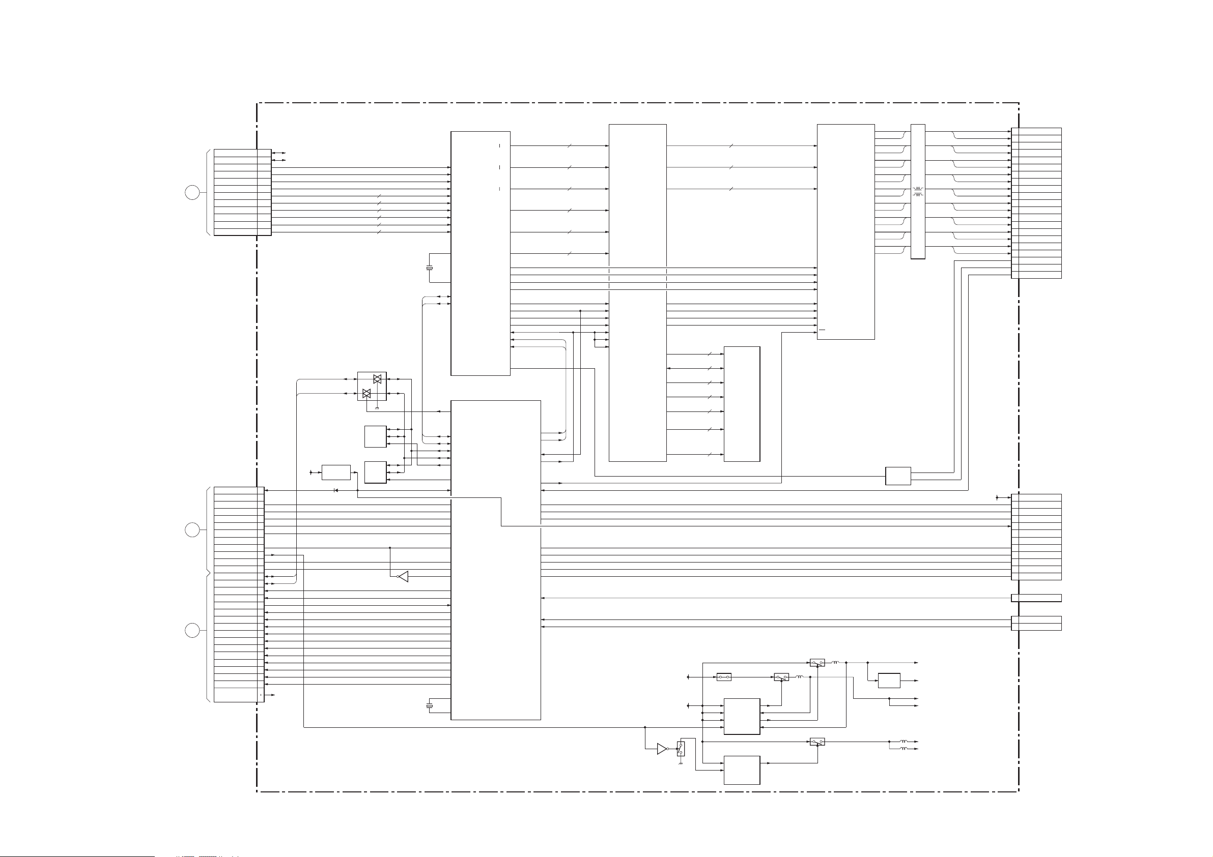
(4) DE3 BOARD
Q
TO
DIC3 BOARD
CN4202
T
TO
A2NU(2/2)BOARD
CN8201
K
TO
K BOARD
CN2603
CN5101
SCL_1
SDA_1
IFPFLDOUT
IFPHS
IFPVS
IFPCK
IFPR1OUT 0-9
IFPG1OUT 0-9
IFPB1OUT 0-9
IFPR2OUT 0-9
IFPG2OUT 0-9
IFPB2OUT 0-9
CN5203
SYS_RESET
THERMO_G/3.3V
FAN_ERROR
FAN_DRY 10
PANEL_ON/DAT_D 11
PS_PROT/CLK_D 12
LOGO 13
D_OVP(NC) 14
PAN_UDP 15
SET_ON_DE 16
PAN_UDM 17
PAN_VBUS 18
DAT_D 23
CLK_D 24
CH_M/S_SW 25
CH_IIC_SW 26
SP_PROT 27
A_MUTE 28
OF_LAG 29
3.3V_SW 30
CH_WP 31
CH_RST 32
M_RST 33
SCLATCH 34
AMP_RST 35
SCLATCH2 36
SCDT 37
SCSHIFT 38
SUB_6.5V
A3
C3
D3
A4
7
8
9
EXT_SDA
EXT_SCL
3
SUB6.5V
6
DE3
IFP_SCL
IFP_SDA
3.3V
IC6001
PSEUDO OUTLINE CORR.
RED
GRN
BLUE
RED
GRN
BLUE
HS
VS
DE
CLK
TRST
PLLS
CLK
EXT_SCL
IFFIELD
IFHSYNC
IFVSYNC
CLK
IFQE 20-29
IFQE 10-19
IFQE 0-9
IFQO 20-29
IFQO 10-19
IFQO 0-9
IC5201
SYSTEM
RESET
D5216
IC5204
BILATERAL
ANALOG SW
2EXT_SDA
5
3
IC5203
NVM
IC5906
NVM
SDA2
SCL2
WP
SDA2
SCL2
WP
10
10
10
10
10
10
7
1
6
5
6
7
5
6
7
Q5205
X5302
33MHz
X5201
6MHz
SDA1
SCL1
SDA1
SCL1
91
65
64
67
66
99
90
92
69
93
95
70
74
73
71
80
82
81
102
101
46
51
100
103
10
19
20
107
108
IC5302
DISPLAY ENGINE
IFFIELD
IFHSYNC
IFVSYNC
CLK
IFQE 20-29
IFQE 10-19
IFQE 0-9
IFQO 20-29
IFQO 10-19
IFQO 0-9
CLKC
XCLKC
BCSDA
ICSCL
SYSTEM CONTROL
BUS_SW0
SDA1
SCL1
SDA2
SCL2
NVM_WP1
5
DITHER
FAN_ERR
FAN
PANELON
ERR2
LOGO
USB_DVP
USB_DVM
USB_VBUS
HCDHX
CH_M/S_SW
CH_IIC_SW
SP PROT
AUDIO MUTE
8
OF_FLAGX
6
K3.3V_SW
CH_HVM_OP
CH_RST
AUDIO RESET PRO
9
SCLATCH
AUDIO RESET AMP
SCLATCH2
SOT1
SCK1
XI
XO
OVRED0
OVRED9
OVGRN0
OVGRN9
OVBLU0
OVBLU9
ONSDATA
ONLE
ONPLE
ONSCK
OVHS
OVVS
OVBLKDE
OVCLK
CLK
ICBLK
ICFREE
INPSS
IC5202
D_DEV_RST
IC FREE
IC BLK
INT_V
D_DEV_RST
PANEL_PD
P_ALARM
SIN0
SDT0
SCK0
BINT
P60
P61
MD0
MD2
WFR_DET
TEMP2
TEMP3
OVRED1
OVGRN1
OVBLU1
OVRED2
OVGRN2
OVBLU2
ONSDATA
ONLE
ONPLE
ONSCK
OVHS
OVVS
OVBLKDE
OVCLK
IC_BLK
ICFREE
61
60
25
50
55
83
11
12
17
104
21
22
89
87
53
40
41
10
10
10
10
10
10
(DISPLAY ENGINE,FPD TRANSMITTER)
ORED
OGRN
OBLU
OHS
OVS
ODE
OCLK
ODAA 0-11
ODA
BDDQA 0-31
ODBAA 0-1
ODBA BA
ODDMA 0-3
ODDQSA 0-3
ODDQS DQS
ODCKEA
ODCKNA
ODCKPA
ODRASNA
ODWENA
ODCASNA
ODCSNA
SUB6.5V
6.5V
Q5909
Q5908
OKRED1
OKGRN1
OKBLU1
A
12
DQODDQ
32
2
DMODDM
4
4
3
4
PS5901
SWITCHING REG.
18
VCC
12
PVCC
1
SEL1
19
STB
SWITCHING REG.
1
VCC
7
CTL/SS
10
10
10
IC5903
DDR SDRAM
IC5904
IC5905
OUT
3
1,2,79,80,
PANEL_PD
Q5901
IC5408
FPD LINK TRANSMITTER
3-10,
81,84
R
93-96,
99,100
G
77,78,
85-92
B
63
B21
69
G25
70
G24
64
B20
54
HSYNC
55
VSYNC
56
DE
11
CLKIN
22
RD
Q5902
Q5907
OH
AOP
A1H
A1P
A2H
A2P
CLK1H
CLK1P
A3H
A3P
A4H
A4P
A5H
A5P
A6H
A6P
A7H
A7P
50
49
47
46
45
44
42
41
39
38
37
36
34
33
32
31
29
28
7
IC5901
1.25V
REG
IC5402
RC
RI-
RS+
L5404-5405
L5407-5413
FILTER
1
2
2.5V_2
1.25VT
3.3V
3.3V_2
1.8V
1.8V_2
PS-
PS+
AO-
AO+
A1-
A1+
A2-
A2+
CK-
CK+
A3-
A3+
A4-
A4+
A5-
A5+
A6-
A6+
A7-
A7+
3.3V
CN5406
4
RA-
5
RA+
6
RB-
7RB+
8RC-
9RC+
11 RCLK-
12 RCLK+
13 RD-
14 RD+
15 RE-
16 RE+
18 RF-
19 RF+
RG-
20
21
RG+
22 RH-
23 RH+
PS-
26
PS+
27
ALARML29
CN5201
3.3V1
SIN
3
SDT
4
SCK
5
RESET6
SCL(NC)7
SDA(NC)8
BINT9
PS010
PS111
MD012
MD213
CN5212
WFR_DET1
CN5207
1
THERMO_2
3 THERMO_3
TO
PANEL
UNIT
TO
JIG
TO
WOOFER
TO
SENSOR
KDE-W50A10 (K) 4-4
Page 29

(5) DIC3 BOARD
I
TO
J1NU BOARD
CN8403
Q
TO
M1U BOARD
CN7552
S
TO
M1U BOARD
CN7553
CN4000 Q4306,4317
CN4002
CN4003
A1
B2
A3
B3
B4
A5
B5
B6
A7
B7
B8
A9
A11
A12
A14
A15
B15
A17
B17
A18
B18
A19
B20
A21
B21
B22
A31
B10,B11
B12
A13
B14
A24-B25
A27-B28
A30,B30
A33-B34
2
3
4
7
8
9
10
13-16
19-22
25-28
31-34
37
38
39
40
43-46
-
49-50
1,2
5-8
11-14
17-20
23-26
29-32
35-38
41
42
43
45
46
47
48
49
I_BINT
MSDIO
MSCK
I2CMSCL1
D_OVP
I2CMSDA1
M_YS
MSBS
USBCONNECT
USBDMNS
I_BOOTMODE
USBDPLS
I_HDMI_ERR
MSDIR
O_HDMI_RESET
UARTTXD1
UARTTXD2
UARTRXD1
MSPI
UARTRXD2
1
SW2.5V
SW3.3V
SW5V
I_BINT
SW3.3V
1
24
IC4609
3.3V
IC4615
34
6
CCPIN_A(CCPYIN_A0-A7)
CCPIN_A(CCPCIN_A0-A7)
I_GXAIN0_A-I_GXAIN7_A
I_GXGIN0_A-I_GXGIN7_A
I_GXBIN0_A-I_GXBIN7_A
I_GXRIN0_A-I_GXRIN7_A
Q4009,4012
SW3.3V
IC4002
I2C_SDA
I2C_SCL
I2C_MSCL1
I2C_MSDA1
I_MAIN_C
B_INT
I_MAIN_CV
O_MSDIO(NC)
I_MSLK(NC)
I_MAIN_R
SET_ON
CLK_W
I_MAIN_B
D_OVP
DAT_W
I_MAIN_G
I_MAIN_YS(NC)
O_MSBS(NC)
I_USBCONNECT
I_USBDMNS
BOOT_MODE
I_USBDPLS
HDMI_ERR(NC)
O_MSDIR(NC)
HDMI_RESET(NC)
I_UARTTXD1(NC)
I_UARTTXDP
I_UARTRXD1(NC)
O_MSPI(NC)
I_UARTRXDP
SYSTEM_RESETX
D_1.8V(NC)
D_1.2V(NC)
D_1.25V(NC)
A_1.8V(NC)
SW_2.5V
SW_3.3V
SW_5V
SUB_6.5V
O_IFPVSOUT
O_IGXHSOUT
O_IGXCKOUT
I_GXYCCKIN
I_GXYCHSIN
I_GXYCVSIN
O_PCCOSOUT
I_GXYIN 0-7
I_GXCIN 0-7
I_GXCKIN
I_GXHSIN
I_GXVSIN
O_PCCLPOUT
I_GXAIN 0-5
I_GXAIN 6,7
I_GXGIN 0-7
I_GXBIN 0-7
I_GXRIN 0-7
CLK_M
DAT_M
M/S_SW
OSDV_M
PC_HPOL
PC_VPOL
OSDH_M
CCPM_MUTE
Q4305,4316
Q4304,4314
Q4303,4313
Q4302,4312
IC4000
1,2
1.2V
7
ENA
IC4001
1,2
1.8V
7
ENA
1.8V
MSDIO
399
MSCK 49
MSBS 290
USBCONNECT 495
USBMNS 42
USBDPLS 168
Q4016
173
43
16
16
6
3
4
Q4006,
Q4007
501
175
594
593
500
141
260
247
463
359
474
243
122
459
371
8
8
8
8
497
396
276
490
161
SW3.3V
UARTRXD2
UARTRXD1
UARTTXD2
UARTTXD1
MSPI
MSDIR
I_HDMI_ERR 393
O_HDMI_RESET 489
I_BOOTMODE 158
S4600
IC4614
1
2
7
1
I2C_SCL SCL
I2C_SDA SDA
14,15
REG
13
14,15
REG
13
REG
IC4610(1/2)
MSDIO
MSCK
MSBS
USBCONNECT
USBMNS
USBDPLS
MSPO
40
GPIO_INT0
UARTRXD2
UARTRXD1
UARTTXD2
50
UARTTXD1
MSPI
MSDIR
GPIO_INT1
GPIO8
GPIO15
EXTGXHSOUT
EXTGXCKOUT
CCPCKIN_A
CCPHSIN_A
CCPVSIN_A
PCCOSOUT
I_GXYIN0-A
-
I_GXYIN7-A
I_GXCIN0-A
-
I_GXCIN7-A
EXTGXCKIN
EXTGXHSIN
EXTGXVSIN
PCCLPOUT
I2CSSCL2
I2CSSDA2
GPIO14
35
GPIO4
GPIO5
GIPO2
VIDEO BUFFER
11
IN2A
8
IN1A
3
SDAI2C_SDA
4
VIDEO BUFFER
13
IN3A
11
IN2A
8
IN1A
3
4
SCLI2C_SCL
Q4000
Q4001IC4301
3,14,16
FP
GPIO7
DRCHSIN
DRCVSIN
CCPYIN_B0
IC4302
OUT2A
OUT2B
OUT1A
OUT1B
IC4303
OUT3A
OUT3B
OUT2A
OUT2B
OUT1A
OUT1B
IC4305
OP AMP
INC+
OUTA
OUTC
IC4803
1.25V
REG
278
252
563
4
21
20
25
24
17
16
21
20
25
24
14
5
7
16
2
6
IC4304
SDRAM
Q4310
Q4309
Q4300,4307
FL4300
L.P.F
Q4301,4308
FL4301
L.P.FINA+
3.3V
2.5V
DQ 0-15
ADDR 0-11
DQM,BA0,BA1
3
XCS,XCAS,XWE
XRAS,CKE,SOCLK
3
3
16
12
1.8V
167
199
196
262
106
197
15
AIN5
13
AIN4
20
AD4 SEL
11
AIN3
AIN2
9
AIN1
69
AOUT2
67
AOUT1
66
FIFOCLK_IN
70
DTOCLK_IN
HDD
VDD
CK2CQ
FIM0
OSDV
46
OSDH
IC4300
OCPX
-
-
7
90
4
28
44
MAIN_D2IN
(M_D2C 2-9)
8
MAIN_D2IN
(M_D2Y 2-9)
8
(M_D2H)
(M_D2V)
(M_D2CLK)
Q4200
1MAIN_CCPYUV
(1MY 2-9)
1MAIN_CCPYUV
(1MC 2-9)
1MAIN_CCPYUV
(1M_CLK/HS/VS)
(1M_CLK/HS/VS)
IC4503
SDRAM
IC4504
SDRAM
IC4004
2
4
1
D2C
D2Y
D9Y RD8
HTIM
VTIM
CLK
XRST
OSDY
IC4202POWER
ON
RESET
3.3V
(1MY 2-9)
8
(1MC 2-9)
8
3
D0_0-31
32
A0_0-10
10
CK0,CS0,WE0
CAS0,RAS0
B0_0_1
D1_0-31
32
A1_0-10
10
CK1,CS1,WE1
CAS1,RAS1
B1_0_1
IC4200
LVDS RECEIVER
RA1
RA8D9C
RD1
--
21
RD0
14
RD6
RCLK-
RCLK+
31
CLKOUT
3
PD
8
8
3
IC4505
DRC MFV1
DIYD0
DIYD7
DICD0
--
DICD7
3
2
2
3
2
2
49
RA-
50
RA+
51
RB-
52
RB+
56
57
59
RD-
60
RD+
DB02
DB09
DR02
DR09
DY212
DY219
DY202
DY209
XRST
CLKI SSCLK
DRCIN
(DRCC1IN 0-7)
-
DRCIN
(DRCC2IN 0-7)
-
DRCIN
(DRCY1IN 0-7)
-
DRCIN
(DRCY2IN 0-7)
-
IC4502
297
4
PLL CLK GEN. PLL CLK GEN.
132
7
SSCLK
PLL CLK GEN.
7
129
2
124
IC4506
SSON
IC4507
SSON
XINCKBI
XIN
10
11
13
14
1
2
4
5
7
8
CN4200
IC4604
3
8
8
13
MRXIN0-
MRXIN0+
MRXIN1-
MRXIN1+
MRXIN2-
MRXIN2+
MRXCLK-
MRXCLK+
MRXIN3-
MRXIN3+
8
8
8
8
7
9
IC4801
ROM
A0-A20
DQ15,A-1
IC4508
CLKD
CLKB
DQ0
-
DQ7
S1
S1
XIN
79.99MHz
P
TO
PD BOARD
CN9502
13
12
4
X4500
D0-D7
8
A0-A21
22
WE,OE,CE
IC4610(2/2)
FP
IC4600
4
X4600
79.99MHz
8
24
IC4608
IC4611
-
IC4613
VOLTAGE
DETECTOR
6.5V 5V 2.5V
PLL CLK GEN.
CLKC
S1
S0
XIN
CLKB
IC4603
PLL CLK GEN.
SSON
XIN
IC4601
SYSTEM RESET
3
CK
RESET
RTC
1
7
1
VS
IC4602
2
47
TALCLKIN GPIO10
GPIO6
587
GPIO_INT3
36
279
388
GPIO0
GPIO3
GPIO6
GPIO11
GPIO12
386
488
I2CMSCLK1
372
IFPFLDOUT
IFPHSOUT
IFPVSOUT
IFPCKOUT
ARM_TDO
ARM_TCK
ARM_TRST
ARM_TDI
ARM_TMS
142
140
13
569
340
543
632
105
227
IFPMSK1OUT
277
13
12
387
GPIO9
9
3
7
4
1
PNLCLKINSSCLK
345
8
RESETX
48
STANDBYX
I2CMSDA1
1
6
IC4614
IFPR1OUT 0-9
IFPG1OUT 0-9
IFPB1OUT 0-9
IFPR2OUT 0-9
IFPG2OUT 0-9
IFPB2OUT 0-9
10
10
10
10
10
10
CN4202
A1
B1
A3
IFPMSK1OUT
B3
C3
D3
A4
B25
IFPR1OUT 0-9
C28
C21
IFPG1OUT 0-9
A25
C16
IFPB1OUT 0-9
B21
A13
IFPR2OUT 0-9
B16
A9
IFPG2OUT 0-9
C12
B4
IFPB2OUT 0-9
D7
CN4600
6
5
4
3
2
CLK_W
DAT_W
IFPFLDOUT
IFPHS
IFPVS
IFPCK
TDO
TCK
TRST
TDI
TMS
1
IC4800
IC4802
DDR MEMORY
32
12
9
ROM_WE/OE/CS1
MCLK1
MCLK1B
MCLK0
MCLK0B
AJ10GPIO
MCSB0
MRASB
MCASB
MMEB
MMD0-63
MMA0-11
MMBA0-MMBA1
2
MDQS0-MDQS7
8
MDQM0-MDQM7
8
204
81
205
82
494
201
317
78
614
DIC3
(LVDS RECEIVER,FP,CCPX,DRC MF)
R
TO
DE3 BOARD
CN5101
KDE-W50A10 (K) 4-5
Page 30

(6) F AND G1 BOARDS
TO
AC INLET
AC IN
CN6001
AC(N)
AC(L)
1
2
F
F6001
L6002-6005
CN6018
2
1
AC(N)
AC(L)
CN6014
2
1
RY6001
Q6915
STBY5V
RY6002
Q6903
RLY5V
PH6904
Q6201,6202
PROTECT
D6100
IC6202
DRIVE
6
CAOUT
8
AC OFF
TH6101
D6106
D6201,
6225 6226
Q6217
16
OUT
15
VCC
9
VREF
3
13
SS
11
VFB
RV6201
D6103
D6208,
Q6209
2
VCC
5
START UP
D6205
RECT
L6201,L6203
Q6203,Q6205
PFC DRIVE
Q6212
Q6213
D6218
LATCH
IC6101
DRIVER
DRAIN
DRAIN
FB
D6216
7
8
4
Q6210
SS
3
OUT
Q6208
IC6204
VREF
D6104
PH6101
D6217
Q6206,6207,6219
PFC SW
IC6201
12V REG
1
VCC
2
CTL
Q6214
OVP
Q6210
LVP
Q6204
SS
T6101
2
1
8
6
4
3
11
10
IC6203
PROTECT
12
13
3
2
5
6
10
9
D6105
Q6215
Q6216
LATCH
14
1
7
8
STBY5V
Q6218
PH6905
RLY5V
STBY5V
CN6017
1
PFC_DET
3
PRI_VCC1
5
PFC_OUT
PRI_GND
2
CN6901
RLY_5V
31RLY_ON
P_SW(-)
5
STBY5V
6
W
TO
G2F BOARD
CN6010
X
TO
G2F BOARD
CN6301
IC6102
VREF
(POWER SUPPLY)G1
KDE-W50A10 (K) 4-6
Page 31

(7) G2N BOARD
W
TO
G1 BOARD
CN6017
X
TO
G1 BOARD
CN6901
CN6010
PFC DET
PRI VCC
PFC OUT
CN6301
RLY 5V
RLY ON
P-SW(-)
STBY 5V 6
T6301
IC6301
DRIVER
15
VC1
Q6418,6419
SUB11V
Q6902
Q6910
Q6502
SW
15
2
F/B
Q6414-6417
4
1
VSENSE
VC1
2
F/B
D6310
STBY5V
CTRL
IC6907D6901
IC6501
DRIVER
1
2
5
1
3
5
D6301
AC-RLY
Q6501
VG(H)
VG(L)
3
1
VG(H)
VS
VG(L)
OCP
VS
OCP
VCC5V
TH6901
23
22
20
16
23
22
20
16
Q6301
CONVERTER
Q6302
CONVERTER
D6308
PH6401
ISOLATER
4
3
STBY5V
PH6902
ISOLATER
1
2
Q6901
PH6905
ISOLATER
4
3
Q6503
CONVERTER
Q6504
CONVERTER
PH6601
ISOLATER
PH6903
ISOLATER
1
2
DC-DC CONV.
4
SUB11V
3
1
2
T6501
3
6
SUB11V
IC6601
VREF
SUB11V
IC6408
PIT
2
4
6
7
OUT2 U
OUT2 D
SBY 2
15
12
10
PIT
17
19
10
Q6918
14
10
13
11
16
15
9
IC6905
Q6919
D6601
RV6601
VD_ADJ
D6406
D6408
D6407,D6417
D6403
Q6405
D6402
D6405
D6404
VCC
5V
Q6903
1
14
Q6906
13
IC6906
VREF
VCC5V
Q6600
Q6601
D6409
Q6406
6
7
9
8
10
11
D6914
D6401
1
Q6915
IC6903 OVP,LVP
7
1
6
4
2
5
Q6909
IC6409
FAN
DRIVE
Q6925,6926
VS
Q6924
Q6923
VS
9
8
11
10
IC6601
VREF
D6912
SUB11V
3
4
14
13
1
Q6413
Q6922
Q6905
Q6913
IC6401
9V REG
IC6403
FAN
DRIVE
IC6402
5V
REG
D6921
3
4
IC6404
D6812
Q6911
Q6407
Q6408
4
13
VCC5V
CN6008
8-10
SUB11V
3.4
SUB6.5V
CN6022
1
FAN ERROR
2
CN6006
1.4
7.10
FAN ERR
2
FAN ERR
5
FAN ERR
8
FAN ERR
11
CN6021
1.4
7
FAN ERR
2,5
FAN ERR
8
CN6009
SUB18V
1
THRU5V
3
5.6
CN6005
1.2 AUDIO25V
CN6004
1
3
AC RLY
4
P-SW(-)
6
STBY5V
7
8
PS PROT
9
REC ON
10
PANEL_ON
11
FAN_ERR
12 FANDRIVE
13
THERMO
TH6403
CN6013
6VD
7
9
10
CN6020
1,2 5V
FAN
FAN
FAN
FAN
SW9V
TU32V
OVP
VD
VS
VS
G
TO
A2NU BOARD
CN2001
TO
FAN
TO
FAN
TO
FAN
F
TO
A2NU BOARD
CN2004
V
TO
K BOARD
CN2602
H
TO
A2NU BOARD
CN2005
TO
PANEL
UNIT
TO
PANEL
UNIT
Q6702
SW2
Q6700
1
15
2
IC6701
DRIVER
VSENSE
VC1
F/B
VG(H)
VS
VG(L)
OCP
VC2
T6701
PIT
3
23
22
20
16
17
D6702
Q6703
Q6704
Q6705
CONVERTER
Q6706
CONVERTER
PH6801
ISOLATER
6
T6702
PIT
3
6
SUB11V
IC6801
VREF
D6801
14
11
14
11
RV6801
VS_ADJ
Q6802
VS
D6802
Q6912
Q6801
G2N
(POWER)
KDE-W50A10 (K) 4-7
Page 32

(8) K BOARD
U
TO
DE3 BOARD
CN5203
CN2603
DAT_D
SLK_D
CH_M/S_SW
CH_IIC_SW
SP_PRT
A_MUTE
OF_FLAG
3.3V_SW
CH_WP
CH_RST
M_RST
SCLTCH
AMP_RST
SCLTCH2
SCDT
SCSHIFT
3
4
5
6
7
8
9
10
11
12
13
14
15
16
17
18
OF_FLAG
SCDT
SSCHIFT
IC2611
4
1
18
5
3
2
SP_PRT
A_MUTE
IC2612
7
NP7
Q2610,Q2611
VCCDET
CONT.SIG.GEN.
XMODE(I)
22
XIN(I)
IC2610
EEPROM
VCC
CH RESET
3.3V
IC2602
RESET
DELAY
IC2600
DATA(O)
LRCK(O)
BLK(O)
ERROR(O)
SDA
SCL
5
6
1
AUDIO L/R
1648
15
14
Q2602
34
DATA(O)
LRCK(O)
BCK(O)
IC2603
DIGITAL AUDIO PROCESSOR
12
I2C_SDA
27
I2CM_S
13
I2C_SCL
9
A_MUTE
SP_PRT
MCLKI
14
SDIN1
38
LRCLK
1
SCLKIN
IC2609
1
75
IC2601(2/2)
2
3
1
3.3V
AUDIO L/R
SDOUT2
SDOUT1
3
4
5
IC2614
2
1
IC2607
12S PWM
32
SCDT
SCSHIFT
OF_FLAG
30
AUDIO L/R
SCDT
SCSHIFT
OF_FLAG
6
X2601
49.152MHz
4
31
DATA OUTL1
19
SOFMUTE
36
XFSIN
21
SCDT
22
SCSHIFT
24
OVFFLAGR
25
OVFFLAGL
23
SCLATCH
29
LRCK
30
BCK
27
INIT
IC2604
12S PWM
31
27
INIT OUTL2
30
BCK
29
LRCK
23
SCLATCH
21
SCDT
22
SCSHIFT
24
OVFFLAGR
25
OVFFLAGL
19
SOFMUTE
36
XFSIN
48
XFSOIN
OUTL2
OUTL1DATA
OUTR1
OUTR2
11
9
AUDIO R
11
9
AUDIO L
6
4
IC2608
PWM WOOFFER DRIVE
2
PWN_BP
17
PWN_AP OUT_A
4
RST
IC2606
PWM AUDIO LCH DRIVE
2
PWN_BP
17
PWN_AP
4
RST
IC2605
PWM AUDIO RCH DRIVE
2
17
PWN_AP OUT_A
4
RST
IC2601(1/2)
10
8
9
OUT_B
DREG
SD
OUT_B
OUT_A
DREG
SD
OUT_BPWN_BP
DREG
SD
5
30
25
8
13
30
25
8
13
30
25
8
13
12
13
AURIO R
AURIO R
W+
L+
L-
R+
R-
Q2608,Q2609
DC
DETECT
Q2605,Q2607
DC
DETECT
Q2604,Q2606
DC
DETECT
1
2
3
4
5
6
CN2601
W+
W-
L+
L-
R+
R-
WOOFFERW-
L
R
J
TO
A2NU(2/2) BOARD
CN2002
CN2600
SPDIF-
SUB11V
5V
AUDIO L/R
6
3
1
X2600
24.576MHz
13
3
2
IC6103
+3.3V REG
CKOUT(O)
DION(I)
13
IC6102
+1.8V REG
Q6101
Q6102
+3.3V
45
+1.8V
K
(AUDIO PROCESSOR,AUDIO DRIVE)
Q2603
D6101
+12V
IC6101
+12V REG
CN2602
1
AUDIO_VCC
2
V
TO
G2N BOARD
CN6005
KDE-W50A10 (K) 4-8
Page 33

(9) H1U, H3, H5 AND M1U BOARDS
T
TO
QM BOARD
CN7304
L
TO
J2NU BOARD
CN8401
CN7650
GRA -
GRA +
GRB -
GRB +
GRC -
GRC +
GRCLK -
GRCLK +
GRD -
GRD +
GRE -
GRE +
CN7005
SUB Y
SUB C
CN7004
REC ATT
D SAP
AD MUTE
CVY MAIN
SUB Y
SUB C
SP MUTE
AC RLY
D OVP
SYSTEM RST
V BUS
IFP BINT
I2CMSDA1(NC)
I2CMSCL1(NC)
DE RST
+B OVP
AFT MAIN
FMONO
I SAP
AFT SUB
TU H MAIN
TU H SUB
AD RST
ATSC RXD
ATSC TXD
ATSC RST
HDMI RST
LINE MUTE
WOOFER MUTE
ANT S
ANT M
POW CTL
SET ON
SIRCS
JIG UDM
JIG UDP
USER RXD
USER TXD
I2C SDA
I2C SLK
B INT
AC DET
STBY 5V
D5
SW3.3V
SW9V
STBY 3.3V
STBY 2.5V
DIC A 1.8V
DIC D 1.8V
CN7001
UVCC
XTRST
XRSTIN
CINIT
DPEAK
ICD 0-3
ICS 0-2
ICLK
1
2
4
5
7
8
10
11
13
14
16
17
A10
A11
A15
A19
A21
A23
A30
A34
A35
A37
A41
A47
A48
A49
A50
B6
B8
B9
B10
B11
B12
B13
B14
B25
B26
B27
B28
B29
B30
B31
B32
B33
B34
B36
B37
B38
B39
B40
B41
I2C SDA-X
B42
I2C SCL-X
B44
B50
A1,A2
STBY5V
B1
A3,A4
SW5V
B3,B4
ATSC5V
A16ATSC 5V
B15,B16
SW3.3V
B17,B18
SW9V
A52
A56
STBY2.5V
A57
DIC A1.8V
A58
DIC D1.8V
A59
ADC 3.3V
A60ADC 3.3V
STBY3.3V
1
2
3
4
5
6-9
10-12
14
M1U
IC7650
MAIN DIN
49
50
51
52
54
55
56
57
59
60
61
62
Q7026,7027,7036
Q7005,7008,7007,7038
Q7018
STBY3.3V
ICD 0-3
ICD 0-2
RA-
RA+
RB-
RB+
RC-
RC+
RCLK-
RCLK+
RD-
RD+
RE-
RE+
PD
Q7028,7029,7037
Q7009
Q7006
Q7710,7714
D7006
4
3
17-22
24-25
26-29
32,33-35
36,45
38-43
7,8
10-15
46,47,31
3
Q7003
Q7604
Q7012
Q7015,2017
Q7025
NC
D7004
D7011
GR 0-7
8
GG 0-7
8
GB 0-7
8
GA 0-7
8
GVS,GHS,GSK
3
45
125
O SAP
146
O AD MUTE
DATA SLICER MAIN
30
DATA SLICER SUB
76
O AC RLY
126
I DOVP
47
O PTE RESET
136
I VSD DET
52
O PF BINT
49
O DERST
127
I ATSC OVP
39
I AFTMAIN
53
O FMONO
121
I SAP
40
I AFTSUB
89
I MAIN H1H
90
I SUB H1H
50
O AD RST/O MS RST
111
I RXD ATSC
112
I TXD ATSC
142
O ATSC RST
141
O HDMI RST
55
O ANT S
54
O ANT M
79
POW CTL
86
I SIRCS
159
UDM
160
UDP
130
I USER RXD
131
O USER TXD
44
I BINTN
143
O SP MUTE
147
O LMUTE2
145
O SPWFR MUTE
83
I-DPEAK
67-70
ICD 0-3
64-66
ICS 0-2
22
ICLK
(MAIN DIN,MPU)
IC7002
SYSTEM UC
MASTER WAIT
I POWER LED
O PICCFF LED
O TIMER LED
O POWER LED
LAMP ERR LED
O ISTBY LED
BUS SW-RST
I IFP BUSY
I CCD MV
I CCD MH
D R0
D R2
D G0
D G2
D B0
D B7
YMOUT
YSOUT
DOT CLK
VSYNC
OSDHSYNC
I CODSV
SUB HSYNC
KEY WAKE
I KEY1
PCSTBY LED
O STBY LED
IO SDAT
IO SCLK
IO SDAT
IO SCLK
O_NVMPR
TRSTX
MD2
SI0
SD0
SCK0
O BUS SW
I RESET
85
88
101
87
171
172
175
176
1
99
3
91
37
104
149
146
119
120
117
153
118
110
108
109
107
106
61
73
80
81
82
48
75
Q7019
5
6
7
IC7003
RESET
Q7022,7024
IC7004
DAT
CLK
WP
54
PSD R5-R7
3
OSD G5-G7
3
OSD B5-B7
3
OSD YM
OSD YS
DOT CLK I
Q7708,7713
Q7704,7709,7715
AMP
X7950
79-99MHZ
XTAL
Q7011,7013
BUS LINE SW
NVM
STBY3.3V
STBY3.3V
Q7002
IGPX1-R0
IGPX1-R7
IGPX1-G0
IGPX1-G7
IGPX1-B0
IGPX1-B7
IGPX1-A0
IGPX1-A7
IGPX1VS/HS/CK
RST
IGPX0-R5
IGPX0-R7
IGPX0-G5
IGPX0-G7
IGPX0-B5
IGPX0-B7
IGPX0-A6
IGPX0-A7
OEX CK
OEX VS
OEX HS
13
AIN4
15
AIN5
OSD V
OSD H
PEF CLKIN
IC7551
MPU
IEX HS
IEX VS
IEX CK
OGPX_HS/VS/CK
IC7701
CCPX
AOUT2
DT0CLKIN
AOUT1
FIF0CLKIN
IC7005
11
10
9
8
1
2
3
4
Q7020
OGPX_R0-R7
8
OGPX_G0-G7
8
OGPX_B0-B7
8
OGPX_A6,A7
2
MASTER WAIT
IFP BUSY
CCDV M
CCDH M
OGPX_A0-A5
6
OGPX_HS/VS/CK
3
1SC2-1 9 OPC BE0-7
1SY2-1 9 OPC GE0-7
1S-CLK/HS/VS OPC CK/HS/VS
Q7700
69
Q7702
FL7700
70
Q7701
67
Q7703
FL7701
66
I2C SCL X
I2C SDA X
SDAT
SCLK
STBY5V STBY3.3V
IC7702
14
15
5
6
IC7001
3.3V
REG
IC7000
2.5V
REG
16
7
8
8
3
IC7700
1.8V
REG
I2C SCLX
I2C SDAX
IC7552
4
I2C SDAS
I2C SLKS
STBY3.3V
1
2
SW5V
STBY5V
DIC A1.8V
DIC D1.8V
CN7553
O GXRIN0
29-32
O GXRIN7
35-38
5-8
O GXGIN0
11-14
O GXGIN7
17-20
O GXBIN0
23-26
O GXBIN7
1 2
O GXAIN6,7
41
O I2CSSCL2
42
O I2CS SDA2
43
M/S SW
44
IFP BUSY
45
OSDV M
48
OSDH M
CN7552
2
I IFPVSOUT
3
I IGXHSOUT
4
I IGXCKOUT
O GXAIN0
43-46
O GXAINS
49,50
O GXCKIN
37
O GXHSIN
O GXVSIN
39
13-16
O GXYIN0
19-22
O GXYIN7
25-28
O GXCIN0
31-34
O GXCIN7
7
O GXYCKIN
O GXYCHSIN
O GXYCVSIN
9
CN7003
4
KEY1
6
P ON
SW5V/THRU
9
STBY5V
10
SIRCS
11
PCSTBY LED
12
PICOFF LED
13
TIMER LED
14
STBY LED
15
POWER LED
16
19 LAMP ERR LED
21
ILINK LED
26
SCL
25
SDA
CN7002
1
STBY3.3V
2
RESET
3
MD2
4
BUSY3
6
SI0
SO0
7
CLK K0
8
S
TO
DIC3 BOARD
CN4003
Q
TO
DIC3 BOARD
CN4002
CN1051
4
6
CN1200
1
1
2
2
3
3
5
5
6
6
7
7
8
8
9
9
D1205
S1056
POWER
S1051
S1055
H1U
Q1201
Q1204
Q1205
D1207
D1206
D1204D1203
Q1203
Q1206
CN1201
H3
STBY5V
1
SIRCS
2
CN1601
1 SIRCS
2
IC1601
H5
KDE-W50A10 (K) 4-9
Page 34

(10) P BOARD
HDMI
AUDIO
HDMI
PC
J9503
L
R
CN9500
D2+
D2-
D1+
D1-
D0+
D0-
CLK+
CLK-
DDC CLK
DDC DAT
DDC +5V
HPD
+5V
IC9514
LPF
Q9511
1
7
IC9503
3.3V
DD CONV.
IC9521
5V
REG
L
R
Q9502
12
14
15
11
4
2
5
1
9
10
IC9506
SW
B
A
+3.3V
13
3
IC9522
5
RESET
+3.3V
4
L
R
4
6
2
AUDIO DAC
2
SCK
3
LRCK
1
SDAT
4
MCLK
IC9517
SUB MICRO
IO-SCL-TV
IO-SDA-TV
REESET-N
IC9500
BUFFER
FSEL
IC9502
O-FCSW
O-ASW2
O-ASW1
12
11
13
16
8
L
5
R
14
22
21
20
36
35
33
32
31
25
11
5
IC9505
FL9501
Q9516
MUTE
FL9504-9506
IC9504
EDID NVM
SCL
SDA
WP
6
5
7
Q9517
IC9509
LEVEL
SHIFT
1
3
4
6
7
9
10
12
15
16
18
19
HDMI RECEIVER
97
RX2+
96
RX2-
92
RX1+
91
RX1-
87
RX0+
86
RX0-
84
RXC+
83
RXC-
76
DSCL
77
DSDA
Q9514
ANGY
ANBPB
ANRPR
SCK
WS
SDO
MCLKOUT
CSCL
CSDA
RESET
12
15
7
32
31
30
26
V
74
75
72
71
X9501
10MHz
Y
PB
PR
27,2834
37
38
24
43
19
41
34
8
9
IO-SCL1
IO-SDA1
O-RESET1-N
I-FMT1
O-HPGMUTE2
I-HPGDET1-N
OSC2
OSC1
+3.3V
3
2
6
5
Q9503,9506
11
13
1
2
3
4
6
7
9
1
2
3
4
5
6
7
8
CN9504
RESET
SCLK
SDAT
CN9505
DEBUG1
DEBUG2
VCC 3.3V
RESET
9V
R
L
PR
PB
Y
P87
P86
P85
NMI
A
TO
A1U BOARD
CN002
P(HDMI)
KDE-W50A10 (K) 4-10
Page 35

(11) QH AND QM BOARDS
MEMORY
STICK
CN7204
BS
DATA0
INS
SCLK
VDD
2
4
6
8
9
QH
IC7202
MS USB
Q7202
Q7201
X7201
48MHz
19
43
31
42
52
53
29
30
BS0
DATA0
SCLK0
SCLK
XIN
XOUT
ON1
LED
VM
VP
SDA
SCL
WP
RESET
46
45
39 6
27 7
IC7201
3.3V
LDO
540
457
IC7203
EEPROM
SDA
SCL
WP
IC7204
RESET
(MEMORY STICK)
CN7201
2
3
TEST
CONNECTOR
VCC/VBUS
D-
D+
CN7303
TXDB
RXDB
3.3VIN
CN7311
11
2
3
1
2
4
FL7300
IC7330
PWR CTL
D3.3V
IC7335
4
IC7325
DDR SDRAM
49
VREF
IC7323
DDR SDRAM
49
VREF
IC7324
DDR SDRAM
49
VREF
IC7322
DDR SDRAM
49
VREF
USB
5
4
26.1621MHz
1
2
IC7326
EEPORM
SCL
SDA
XWC
IC7321
GFX PLL
SCL
SDA
HSO
VSO
CLK
I2CA_SCL
I2CA_SDA
D0-D7
D24-D31
A0-A14
/WE,/CAS,CKE
/RAS,/CSO
D8-D23
D0-D7
D24-D31
A0-A14
/WE,/CAS,CKE
/RAS,/CSO
D8-D23
MEM_VREF
D5V
X7300
IC7315
42
1
Q7308
D3.3V
IC7336
1
4
2
6 547
5
7
3
2
11
14
12
16
15
5
16
15
5
16
15
5
16
15
5
526
555
556
515
516
386
376
475
563
461
553
504
533
486
44
IC7300
USBPA
USBNA
USBOVRUR
XTALIN
XTALOUT
PCICLK
CLKOUT0
PDB
TDB
IDE_INTRQ
IDE_DMARQ
VCOX_INA
DQB
AB
DQA
AA
VREF
DAC4
DAC6
DAC5
GPIOB0
GPIOB1
GPIOA7
/FRDY
FSTB
RESET#
SMCCLK
SMDATAA
NRSSCLKAA
SMCLKA
RESETOUT
ACRESET#
ACXTAL_OUT
SMDATAS
VCXO_INB
TDATA0
TCLKA
TVLDA
TSTRTA
VDDP
VDDR3
ACSYNC
AVDD 1/2
A2VDD 1/2
XMVDD
PMIVDD
VDDDI
APVDD
VDDC18
PCIVREF
A2VDDQ
VDDR1
TDA
RDA
536
564
535
452
454
518 MCK 4
492
311 DVDVSYNC 33
177 DVOGA0
156
363 19
550
464
554
468
187
514
388
368
397
389
522 SPDIFA
524
479,480 DAC_A2.5V_PRI
534
450,476
459
267,441
131,257
393
406
407
Q7301-7303
2
DVOGA1
DVOGA2350
DVOGA3159
AD0-15
ICS0-5
/RD,/WE
BE0-1,ALE0-1
6
IC7318,7319
FLASH MEMORY
/WP I/O
/CE
D7306
Q7300
DAC_DL8V
MUTE
IC7305
RESET
16
6
AD0-7
/RD,/WE,BE0-1
ALE0
9
IC7312
REG
DAC_A2.5V_SEC506,507
PLL_XM1.8V15
PLL_PM1.8V
PLL_AP1.8V
VDD_IO1.8V
DAC_REF1.8V447
D2.5V
D1.5V
IC7327
ADC
8
AOUTL
MCLK
1DATA489
SDATA
3LRCK460
LRCK
2/AUD-DEMPH2370
SCLK/DEM
3
1
BUS LINE(AD0-AD15)
BUS LINE(/CS0-5)
BUS LINE
(BE0-1,/WE,/RB,CLK,ALE0-1)
8
5
BUS SEL1
BUS SEL0
D3.3V
IC7314
1.8V LDO
IC7313
1.8V LDO
IC7312
1.8V LDO
IC7311
1.8V LDO
IC7310
1.8V LDO
IC7309
1.5V REGVDDC
AOUTR
Q7304
DVOGA0-3
IC7331
F.F
/RD 5
/CE
D3.3V
D2.5V
5
GA1,3,5,7
AD8-15
/CS1-5
IC7320
SERIAL EEPROM
2/WE
/S
Q
D
Q7305
B2-B9
GA0-GA7
G2-G5
1
6
O
8
5
IC7306
42
IC7307
8
8
4
AD8-15
8
/CS2-5
ALE1
4
IC7316
BUS SW
3
5
6
13
10
S1 S0
SYNC PWM CONTROL
5
HDRV
3
LDRV
1
FB
24
SYNC PWM CONTROL
5
HDRV
3
LDRV
1
FB
IC7332
LVDS TRANSMITTOR
VCC
VCC
TE+
TE-
TD+
TD-
TCLK+
TCLK-
TC+
TC-
TB+
TB-
TA+
TA-
/CS0
7
CLK
9
2
2
34DVDHSYNC310
13/RESET_SYSTEM
/PDWN
24
IC7301
IC7302
18
19
20
21
22
23
24
25
28
29
30
31
I2CA_SDA
I2CA_SCL
AD0-AD7
BE1
BE0
/RD
1
CN7309
3
7
11
2
4
12
8
CN7304
1
2
4
5
7
8
10
11
13
14
16
17
CN7306
18,20
22,24
26,28
8
30,32
6
8
1210HRW
3
4
142HIRQ#
16
34
36
38
40
1
CN7307
4
7,8103.3V
CN7300
9,10 +9V
5 +5V
3
2
1
PR_OUT
PB_OUT
Y_OUT
HS_OUT
VS_OUT
AUDIO_LOUT
AUDIO_ROUT
TE+
TE-
TD+
TD-
TCLK+
TLCK-
TC+
TC-
TB+
TB-
TA+
TA-
HD0
HD7
HA1
HA0
CS0
RESET_FE
RESET2099
HACK
FE_SDATA
FE_SCLK
FE_VAL
FE_SYNC
FE_SDA
FE_SCL
9V2
5V
2.5V
BOX_RST_IN
TV_TXD
TV_RXD
O
TO
A1U BOARD
CN006
T
TO
M1U BOARD
CN7650
Z
TO
QT BOARD
CN7306
P
TO
QT BOARD
CN7902
M
TO
A2NU BOARD
CN8208
(AVOUT,POWER,USB,LVDS)
QM
KDE-W50A10 (K) 4-11
Page 36

(12) QT BOARD
Z
TO
QM BOARD
CN7306
CN7900
FE_SDA
FE_SEL
RESET_FE
RESET_2099
HA1
HA0
CS0
HRW
HIRQ#
HACK
HD0
HD7
FE_SDATA
FE_SCLK
FE_VAL
FE_SYNC
10
12
14
16
18
32
34
36
38
40
1
2
3
4
6
8
FE_SDA
FE_SCL
/RESET_FE
HD0-HD7
8
D7901
Q7902 MPEG_ERR
Q7906
D7902
+3.3V
D7900
2.5V
+9V
IC7905
IC7901
DC_DC
CONVERTER
POD INTERFACE CONTROL
7
RESET#
11
HA1
12
HA0_I2CA0
15
HIR0#
16
HACK
HD
27
TOD
28
TOCLK
29
TOVAL
30
TOSTRT
5
CLK
TICLK
4
VALID
TIVAL
96
DATA
TIDO
CLK
MPEG_CLK
VALID
MPEG_ENABLE
DATA
MPEG_D7/
FE_SCL
FE_SDA
/RESET_FE
D3.3V
DEM_SL
DEM_SDA
RESET
FDC_LOCK
FAT_LOCK
D1.2V_DEM1.2V REG
A32V_TU
IC7900
HRW_SCL
HCS_SDA
TU7901
TUNER
HD
MDI
MCLKI
MIVAL
MCLKO
MISTRT
MOVAL
MOSTRT
WAIT#
RST
IREQ#
WE#
IOWR#
IORD#
VS1#
OE#
ADOE
A
D
CD#
CE1#
VCCSW
A4_CTX
A5_ITX
A6_ETX
A7_QTX
A8_CRX
A9_DRX
VCCSEL
IF_OUT
SAP_IND_I
ST_IND_I
MODE_O
F_MONO_O
POD_CRX
POD_DRX
AGC_IN
AGC_OUT
TU_SDA
TU_SDA0
TU_SCL
TU_SCL0
AGC_SW
HD0-HD7
8
MDI0-MDI7
95
94
82
93
81
80
68
69
67
61
59
60
70
62
66
6
18
44
CSO#
45
+9V
+5V
+3.3V
40
41
16
19
39
34
33
32
31
28
27
24
26
Q7901
15
14
12
Q7900
HRW
HRW#
HCS#
CD#
CE1#
VCCSW
A4_CTX
A5_ITX
A6_ETX
A7_QTX
A8_CRX
A9_DRX
FDC_CRX
FDC_DRX
4
5
2
14
13
71
58
33
40
41
42
43
46
47
34
8
A0-A3,A10-A11
D0-D7
IC7904
PLD
A
CD2#
CD1#
CE1_OUT#
BVCC5#
VCCSEL
Q7904
IC7902
3
1
13
9,10,11
8
A4-A9
6
14
46
47
IC7903
15
38
POWER I/F SW
27
BVCC5#
26
BVCC3#
NTSC_STEREO_DEMODULATOR
VIF
SAP_IND
ST_IND
MODE
Q7903
F_MONO
RF AGC
AVCC
BVCC
TU7900
LOUT
ROUT
AFCONT
+5V
12
Q7905
+9V
+5V
+3.3V
+2.5V
CN7103
5,7,9
66,68
71,73
75
27,30
32,34
46,48
50,52
MCLKI
33
MIVAL
35
MCLKO
51
MISTRT
55
MOVAL
14
11
MOSTRT
WAIT#
21
RESET
23
47
IREQ#
49 WE#
IOWR#
57
59
IORD#
62 VS1#
63
64 CE2#
13,15
17,19
22,24
26,29
56,58
60,65
6,8
10,70
72,74
76,78
3
77
41-45
VPP-2
36-40
CN7904
1,2 VCC
5
CN7901
2
6
4
AFT_M
1
9
8
10
AGC M
CN7902
2
4
10
MDO0
MDO7
MDI0
MDI7
OE#
A0
A11
D0
D7
CD2#
CD1#
CE1#67
VCC
VPP
TU1VDET OUT2
TU1L
TU1R
SDA
SCL
9V
5V
3.3V
2.5V
N
TO
A1U(1/2)BOARD
CN005
A2NU(2/2)BOARD
Y
CN8210
P
TO
QM BOARD
CN7307
TO
(TUNER,POD INTERFACE CONTROL)
QT
KDE-W50A10 (K) 4-12
Page 37

SIRCS
S
S
GND2
GND
SIRCS
S
SUB6.5VGND
CHM/S SWPO
GND2
OGTC
C
GND
OR
GND
U
C-
O
G
GNDPSPROTGND
3.3VSWS
OGO
CHRST
GND
GND
STS
GND
US
SCDT
S
GND
SCS
GND3
GND
GND
GND2
GND
SUB6.5V616
SUB6.5V919
SUB6.5V323
SYSRESET626
OR33
V3333
93
93
OGO
UDP646
SETO
949
US3535
GND6565
GND66
GND3636
CHM/S SW
UTE979
CHWP6868
SCLTCH39
39
SCDT1010
SCS
040
GND100100
313
343
03103
04104
545
575
646
07107
878
949
979
020
50
50
0110
818
52529V9
8282SC
323RESETS
5353GND
GND
3113LGND
GND
5VGND
4114
8585GND2.5VGND
56
56
7117
828CRCR
8888C/C
59
59
89
89
3030SS
6060S
0120
C
9
3
5
6
8
8
9
0
S
C
5
5
3
5
55
6
5
58
9
60
6
63
5
9
66
GND
GND
8
3.3
69
30
3
33
3
5
36
3
8
39
0
80
V
(N)
V
V
V
V
V
V
V
V
T
V
K
T
T
V
V
V
V
V
T
V
V
V
T
Y
(5P)
Y
V
V
Y
T
K
V
V
V
V
V
W
Y
T
V
V
V
V
V
S
S
T
Y
T
P
V
V
E
V
E
V
V
V
V
V
T
T
L
E
V
T
G
K
V
V
L
V
T
S
K
T
V
S
K
T
S
X
V
T
V
V
V
V
V
T
T
P
Y
W
Y
T
T
T
T
V
V
V
#
V
V
V
S
L
K
Y
A
L
A
X
K
L
V
K
A
T
A
Y
X
T
T
T
T
T
4-2. FRAME DIAGRAMS
K
CN2600
15.0V
2
GND
SUB11V
3
4GND
5
SPDIF+/NC
6
SPDIF-
7GND
7P
CN2601
1W+
2W3
L+
4L-AMP_RS
5R+
6R-
6P
GND
Speaker R
1R+
2R-
Speaker L Woofer
1L+
2L-
Woofer Connector
1W+
2W-
WFR_DET
3
4GND
CN2603
GND
DAT_D 3
SLK_D
CH_M/S_SW 5
CH_IIC_SW 6
SP_PROT 7
A_MUTE
OF_FLAG
3.3V_SW 10
CH_WP 11
CH_RST
M_RST 13
SCLTCH 14
SCLTCH2
SCDT
SCSHIFT
GND 19
GND
20P
CN2602
AUDIO_VCC
AUDIO_VCC 2
GND
GND
5P
W+
WFR_DET 3
GND
NC 3
Panel
CN301
NC
1
2GND
3
GND
4GND
5GND
6VD
7
VD
8NC
9VS
10 VS
CN302
15V
25V
3GND
4GND
CN101
G2N
CN6020
5V
1
25V
GND
3
4GND
CN6024
1 FAN
2 FAN_ERR 2
1 FAN
2 FAN_ERR
3GND
CN6021
1 FAN
2 FAN_ERR
3GND
5 FAN_ERR
6GND
7 FAN
8 FAN_ERR
9GND
CN6006
1 FAN
2 FAN_ERR
3GND
4 FAN
5 FAN_ERR
6GND
7 FAN
FAN_ERR8
9GND
FAN
10
12 GND
CN6301
1 RLY_5V
2GND
3 RLY_ON
4GND
5 P_SW(-)
6 STBY5
CN6010
1 PFC_DET
2PRI_VCC1
3PRI_GND
4NC
CN6005
AUDIO_25V 1
AUDIO_25V 2
NC
AUDIO_GND
CN6013
NC 1
GND
GND
GND 4
GND 5
NC 8
CN6023
GND 1
CN6004
TU32V 1
GND 2
AC RLY 3
P_SW(-) 4
GND
STBY5
OVP 7
PS PRO
REC_ON 9
PANEL_ON 10
FAN_ERR 11
FANDRIVE 12
THERMO_G 13
CN6008
GNDW-111 FAN_ERR
GND
SUB 6.5
SUB 6.5
GND
GND
GND 7
SUB 11
SUB 11V9
SUB 11
CN6009
SUB 18
GND 2
THRU 5V 3
GND
SW 9
SW 9
GND 75 PFC_OUT
G1
CN6017
1 PFC_DET
2PRI_VCC1
3PRI_GND
4NC
5 PFC_OUT
CN6901
1 RLY_5V
2GND
3 RLY_ON
4GND
5 P_SW(-)
6 STBY5
CN6014
1AC(L)
2AC
F
CN6018
1AC(L)
2AC(N)
CN6001
CN6051
CN6052
AC(N) 1
AC(L)
H3
CN1200
VPI
THR
SW_5V
1
TBY5V2 TIMERLED
STBY5
N
1GND
N
2
DATD TIMERLED
LK
4
HIICSW PON
PPR
T
TE TC+ PANELON T
AM
8
FFLA
9
HW
12
MR
T PI
LT
H TIMERLED TD+ PAN
AMPR
15
LT
H
16
17
HIFT
18
20
CN1201
1
STBY5
2
SIRCS
3
E
H5
2
E
4 GND
PI
FFLED
5
SHOUGA_LED
6
TSUSHIN_LED
TBYLED KEY1 TB-
7
STBY_LED
WERLE D
8
POWER_LED
9
REC_LED
ND
10
E
CN1601
1
STBY5
2
SIRCS
3
E
H3 Connector
THRU5V
1
TBY
V2
3
4
FFLED KEY1
5
6
TBYLED PON
7SIRCS 3
P
WERLE D
8
9
ND
10
H1
1
4
VD
VDCN6022
VS 9
VS 10
E1
E
5GND
1
2
4
LVDS
1
2
3
4
5
6
7
8
9
10
11
12
13
14
15
16
17
18
19
20
21
22
23
24
25
26
27
28
29
30
31
3
5
33GND
6
7
5
6
8
2
3
4
5
6
8
10
1
4
5
6
2
1
DE3
CN5203
GND
1
N
GND
2
3
SUB6.5
4
SUB6.5
B.V
5
SUB6.5
6
SUB6.5
7
SYSTEM_RESE
THERM
8
THERMO_G/3.3V
FANERR
9
FAN_ERROR
FANDR
10
FAN_DRV
PANEL
N
11
PANEL_ON/DAT_D
PSPROT
12
PS_PROT/CLK_D
L
13
LOGO
VP
D
14
D_OVP
PAN
15
PAN_UDP
NDE
16
SET_ON_DE
DM
PAN
17
PAN_UDM
PANVB
18
PAN_VBUS
19
GND
N
20
GND
21
GND
22
GND
DATD
23
DAT_D
LK
24
CLK_D
25
CH_M/S_SW
HII
W
26
CH_IIC_SW
PPR
T
27
T
SP_PRO
AM
28
A_MUTE
FFLA
29
OF_FLAG
.VW
30
3.3V_SW
31
CH_WP
HR
32
CH_RST
MR
T
33
M_RST
34
SCLTCH
AMPR
T
35
AMP_RS
LT
H
36
SCLTCH2
37
SCDT
HIFT 4
38
SCSHIFT
N
39
GND
40
GND
40P
CN5406
1
GND(NC)
2
GND
3
GND
4
RARA+
5
6
RB-
7
RB+
8
RC-
9
RC+
10
GND
11
RCLKRCLK+
12
13
RD-
14
RD+
RE-
15
RE+
16
17
GND
18
RF-
19
RF+
RG-
20
RG+
21
22
RHRH+
23
GND
24
25
MSE
PS-
26
PS+
27
GND
28
ALARML
29
GND
30
GND
31
31P
CN5201
1
3.3V
2
GND
3
SIN
SOT
4
5
SC
RESE
6
SCL
7
SDA
8
9
BINT
P60
10
11AUDIO_GND 4
P61
MID0
12
MID2
13
CN5202
NON_PANEL_MOD
1
5V/3.3
2
SIRCS/BIN
3
GND
4
1.8V
5
CN5402
MAX_PLS1/SCL_JIG
1
MAX_PLS2/SDA_JI
2
DITHER/BINT
3
POWER
4
5
PNL_MUTE
6
GND
MAS
7
STATUS
84 FAN
CN5213
DEW_Det
1
NC
2
3
GND
CN5212
1
WFR_DET
2
GND
FAN 1
FAN
3
2
FAN_ERR
GND
1
FAN 2
FAN
3
FAN_ERR
2
GND
1
FAN 3
FAN
3
FAN_ERR
2
GND
1
FAN 4
FAN
3
FAN_ERR
2
GND
1
FAN 5
FAN
3
FAN_ERR
2
GND
1
FAN 6
FAN
3
2FAN_ERR
GND
1
AC INLET
AC(N)1
2AC(L)
GND
GND
GND
Sensor
Sensor
FAN 7
IFPFLDOUT
IFPMSK1OU
IFPB2OUT0
IFPB2OUT1
IFPB2OUT2
IFPB2OUT3
IFPB2OUT4
IFPB2OUT5
IFPB2OUT6
IFPB2OUT7
IFPB2OUT8
IFPB2OUT9
IFPG2OUT0
IFPG2OUT1
IFPG2OUT2
IFPG2OUT3
IFPG2OUT4
IFPG2OUT5
IFPG2OUT6
IFPG2OUT7
IFPG2OUT8
IFPG2OUT9
IFPR2OUT0
IFPR2OUT1
IFPR2OUT2
IFPR2OUT3
IFPR2OUT4
IFPR2OUT5
IFPR2OUT6
IFPR2OUT7
IFPR2OUT8
IFPR2OUT9
IFPB1OUT0
IFPB1OUT1
IFPB1OUT2
IFPB1OUT3
IFPB1OUT4
IFPB1OUT5
IFPB1OUT6
IFPB1OUT7
IFPB1OUT8
IFPB1OUT9
IFPG1OUT0
IFPG1OUT1
IFPG1OUT2
IFPG1OUT3
IFPG1OUT4
IFPG1OUT5
IFPG1OUT6
IFPG1OUT7
IFPG1OUT8
IFPG1OUT9
IFPR1OUT0
IFPR1OUT1
IFPR1OUT2
IFPR1OUT3
IFPR1OUT4
IFPR1OUT5
IFPR1OUT6
IFPR1OUT7
IFPR1OUT8
IFPR1OUT9
THERMO_2
THERMO_3
FAN_ERR
CN5101
SDA_1
CN5207
SCL_1
IFPHS
IFPV
IFPC
GND
GND
GND
GND
GND
GND
GND
GND
GND
GND
GND
GND
GND
GND
GND
GND
GND
GND
GND
GND
GND
GND
GND
GND
GND
GND
GND
GND
GND
GND
GND
GND
GND
GND
GND
GND
GND
GND
GND
GND
GND
GND
GND
GND
GND
GND
GND
GND
GND
GND
GND
GND
GND
GND112
GND
FAN
GND
1
A1
1
B1
C1
D1
2
A2
B2
C2
2
D2
A3
B3
C3
D3
4
A4
4
B4
C4
D4
A5
B5
C5
D5
A6
B6
C6
D6
7
A7
7
B7
7
C7
D7
A8
B8
C8
D8
A9
B9
C9
D9
A10
B10
7
C10
D10
11 11
A11
41 41
B11
71 71
C11
101
D11
12 12
A12
42 42
B12
72 72
C12
1
D12
1
A13
4
B13
7
C13
1
D13
14 14
A14
44 44
B14
74 74
C14
1
D14
1
A15
4
B15
7
C15
1
D15
1
A16
4
B16
7
C16
1
D16
17 17
A17
47 47
B17
77 77
C17
1
D17
1
A18
4
B18
7
C18
1
D18
1
A19
4
B19
7
C19
1
D19
2
A20
B20
C20
11
D20
21 21
A21
1
B21
C21
111 111
D21
22 22
A22
B22
C22
11
D22
2
A23
B23
C23
11
D23
24 24
A24
4
B24
4
C24
11
D24
2
A25
B25
C25
11
D25
2
A26
B26
C26
11
D26
27 27
A27
7
B27
7
C27
11
D27
2
A28
B28
C28
11
D28
2
A29
B29
C29
11
D29
A30
B30
C30
12
D30
3
4
1
2
1
2
3
2
1
DIC3
B to B
CN4202
1
CLK_W
A1
1
B1
DAT_W
1
GND
C1
1
GND
D1
2
A2
GND
2
B2
GND
2
C2
GND
2
D2
GND
A3
IFPFLDOUT
B3
IFPMSK1OU
IFPHS
C3
IFPV
D3
4
IFPC
A4
4
IFPB2OUT0
B4
4
C4
IFPB2OUT1
4
D4
IFPB2OUT2
A5
GND
GND
B5
GND
C5
D5
GND
IFPB2OUT3
A6
B6
IFPB2OUT4
C6
IFPB2OUT5
GND
D6
7
IFPB2OUT6
A7
7
B7
IFPB2OUT7
7
C7
IFPB2OUT8
7
D7
IFPB2OUT9
GND
A8
GND
B8
GND
C8
GND
D8
IFPG2OUT0
A9
B9
IFPG2OUT1
C9
IFPG2OUT2
D9
IFPG2OUT3
A10
IFPG2OUT4
B10
IFPG2OUT5
7
C10
IFPG2OUT6
D10
GND
GND
A11
GND
B11
C11
GND
101
GND
D11
IFPG2OUT7
A12
B12
IFPG2OUT8
C12
IFPG2OUT9
1
GND
D12
IFPR2OUT0
A13
B13
IFPR2OUT1
7
C13
IFPR2OUT2
D13
IFPR2OUT3
GND
A14
GND
B14
GND
C14
GND
D14
1
IFPR2OUT4
A15
B15
IFPR2OUT5
C15
IFPR2OUT6
1
D15
IFPR2OUT7
1
A16
IFPR2OUT8
B16
IFPR2OUT9
7
IFPB1OUT0
C16
1
GND
D16
GND
A17
GND
B17
GND
C17
GND
D17
1
IFPB1OUT1
A18
4
B18
IFPB1OUT2
C18
IFPB1OUT3
1
GND
D18
1
IFPB1OUT4
A19
B19
IFPB1OUT5
C19
IFPB1OUT6
1
D19
IFPB1OUT7
GND
A20
GND
B20
GND
C20
D20
GND
IFPB1OUT8
A21
1
B21
IFPB1OUT9
1
C21
IFPG1OUT0
D21
IFPG1OUT1
A22
IFPG1OUT2
B22
IFPG1OUT3
C22
IFPG1OUT4
11
GND
D22
GND
A23
B23
GND
GND
C23
D23
GND
IFPG1OUT5
A24
4 PR
B24
IFPG1OUT6
4
C24
IFPG1OUT7
D24
IFPG1OUT8
2
A25
IFPG1OUT9
B25
IFPR1OUT0
C25
IFPR1OUT1
11
D25
IFPR1OUT2
2
GND
A26
GND
B26
GND
C26
11
D26
GND
IFPR1OUT3
A27
7
B27
IFPR1OUT4
7 Y
C27
IFPR1OUT5
D27
IFPR1OUT6
A28
IFPR1OUT7
B28
IFPR1OUT8
C28
IFPR1OUT9
11
D28
GND
2
A29
GND
B29
GND
GND
C29
11
D29
GND
GND
A30
B30
GND
C30
GND
D30
GND
120P
CN4201
MRXIN0-
2
MRXIN0+
3
DRAIN
4
MRXIN1-
5
MRXIN1+
6
DRAIN
7
MRXIN2-
8
MRXIN2+
9
DRAIN
10
MRXCLK-
11
MRXCLK+
12
DRAIN
13
MRXIN3-
14
MRXIN3+
14P
CN4200
1
MRXIN0-
2
MRXIN0+
3
DRAIN
4
MRXIN1-
5
MRXIN1+
6
DRAIN
7
MRXIN2-
8
MRXIN2+
9
DRAIN
10
MRXCLK-
11
MRXCLK+
12
DRAIN
13
MRXIN3-
14
MRXIN3+
14P
CN4600
1
GND
2
TMS
3
TDI
4
TRST
5
TCK
6
TDO
6P
H1 Connector
ND1
12
TBY5V1
2
3
4
5
6
7
CN1001
ND1 P
1
E
TBY5V1 TE+
2
STBY5
3
KEY-WAK
KEY1
4
KEY1
E
5
PON
P-ON
P-SW(-)67
CN4002
GND
1
2
O_IFPVSOU
O_IGXHSOUT
3
O_IGXCKOUT
4
GND
5
GND
6
I_GXYCCKIN
7
I_GXYCHSIN
8
I_GXYCVSIN
9
O_PCCOSOUT
10
GND
11
GND
12
I_GXYIN0
13
I_GXYIN1
14
I_GXYIN2
15
I_GXYIN3
16
GND
17
GND
18
I_GXYIN4
19
I_GXYIN5
20
I_GXYIN6
21
I_GXYIN7
22
GND
23
GND
24
I_GXCIN0
25
I_GXCIN1
26
I_GXCIN2
27
I_GXCIN3
28
GND
29
GND
30
I_GXCIN4
31
I_GXCIN5
32
I_GXCIN6
33
I_GXCIN7
34
GND
35
GND
36
I_GXCKIN
37
I_GXHSIN
38
I_GXVSIN
39
O_PCCLPOUT
40
GND
41
GND
42
I_GXAIN0
43
I_GXAIN1
44
I_GXAIN2
45
I_GXAIN3
46
GND
47
GND
48
I_GXAIN4
49
I_GXAIN5
50
50P
CN4003
I_GXAIN6
1
2
I_GXAIN7
GND
3
GND
4
I_GXGIN0
5
I_GXGIN1
6
I_GXGIN2
7
I_GXGIN3
8
GND
9
GND
10
I_GXGIN4
11
I_GXGIN5
12
I_GXGIN6
13
I_GXGIN7
14
GND
15
GND
16
I_GXBIN0
17
I_GXBIN1
18
I_GXBIN2
19
I_GXBIN3
20
GND
21
GND
22
I_GXBIN4
23
I_GXBIN5
24
I_GXBIN6
25
I_GXBIN7
26
GND
27
GND
28
I_GXRIN0
29
I_GXRIN1
30
I_GXRIN2
31
I_GXRIN3
32
GND
33
GND
34
I_GXRIN4
35
I_GXRIN5
36
I_GXRIN6
37
I_GXRIN7
38
GND
39
GND
40 GND
CLK_M
41
DAT_M
42
M/S_S
43
IFP_BUS
44
OSDV_M
45
PC_HPOL
46
PC_VPOL
47
OSDH_M
48
CCPS_MUTE
49
GND
50
50P
CN4000
1 R2
A1
I_MAIN_C
41
B1
GND
2
GND
A2
42
B_INT
B2
I_MAIN_CV
A3
4
O_MSDIO
B3
4
GND
A4
44
K
O_MSC
B4
I_MAIN_R
A5
4
SET_ON
B5
A6
GND
4
B6
CLK_W
7
I_MAIN_B
A7 A7
47
D_OVP
B7
GND
A8
4
DAT_W
B8
I_MAIN_G
A9
4
GND
B9
1
GND
A10
D_1.8V
B10
11
A11
I_MAIN_Y
1
D_1.8V
B11
12 Y2
O_MSBS
A12
2
D_1.2V
B12
1
D_1.25V
A13
GND
B13
14
A14
I_USBCONNECT
SYSTEM_RESET
O_A_IFPHSOUT
O_A_IFPVMOU
80P
4
B14
A_1.8V
1
I_USBDMNS
A15
BOOT_MODE
B15
1
GND
A16
GND
B16
17 R2
I_USBDPLS
A17
7
HDMI_ERR
B17
1
O_MSDIR
A18
HDMI_RESET
B18
1
I_UARTTXD1
A19
GND
B19
2
GND
A20
I_UARTTXDP
B20
21
I_UARTRXD1
A21
1
O_MSPI
B21
22
A22
2
I_UARTRXDP
B22
2
A23
GND
GND
B23
24
SW_2.5V
A24
4
SW_2.5V
B24
2
SW_2.5V
A25
SW_2.5V
B25
2
GND
A26
GND
B26
27
SW_3.3V
A27
7
SW_3.3V
B27
2
SW_3.3V
A28
SW_3.3V
B28
2
GND
A29
GND
B29
SW_5V
A30
7
SW_5V
B30
1
A31
71
NC
B31
2
GND
A32
72
GND
B32
SUB_6.5V
A33
7
SUB_6.5V
B33
4
SUB_6.5V
A34
74
SUB_6.5V
B34
O_IFPAGOUT
A35
7
B35
GND
A36
7
GND
B36
7
O_IFPABOU
A37
77
O_A_IFPVSOU
B37
GND
A38
7
GND
B38
A39
O_IFPAROUT
7
B39
4
A40
GND
B40
M1U
CN7003
ND1 TA-
1
GND
TBY
V1 TA+
2
STBY_5
3
KEY_WAK
4
KEY1
56GND
P_ON
P_SW
7
NC
8
THRU5V
910THRU_5V
TBY5V2 TCLK- L
STBY_5
IR
SIRCS
11
12
PCSTBY_LED
FFLED TD
PICOFF_LED13
TIMER_LED
14
TBYLED
15
STBY_LED
WERLE D TE-
POWER_LED
16
REC_LED
17
GND
18
LAMP_ERR_LED
19
NC
20
ILINK_LED
21
ILLUM_LED
22
GND
23
GND
24
SDA3025
SCL
26
GND
27
NC
28
NC
29
KEY2
CN7552
1
GND
2
I_IFPVSOU
I_IGXHSOUT
3
I_IGXCKOUT
4
GND
5
GND
6
7
O_GXYCCKIN
O_GXYCHSIN
8
O_GXYCVSIN
9
I_PCCOSOUT
10
GND
11
GND
12
O_GXYIN0
13
14
O_GXYIN1
O_GXYIN2
15
O_GXYIN3
16
17
GND
GND
18
19
O_GXYIN4
20
O_GXYIN5
O_GXYIN6
21
22
O_GXYIN7
GND
23
24
GND
O_GXCIN0
25
26
O_GXCIN1
O_GXCIN2
27
28
O_GXCIN3
GND
29
30
GND
O_GXCIN4
31
32
O_GXCIN5
33
O_GXCIN6
O_GXCIN7
34
GND
GND3536
37
O_GXCKIN
38
O_GXHSIN
3940O_GXVSIN
I_PCCLPOUT
41
GND
GND
42
43
O_GXAIN0
O_GXAIN1
44
45
O_GXAIN2
O_GXAIN3
46
47
GND
GND
48
49
O_GXAIN4
O_GXAIN5
50
CN7553
O_GXAIN61
O_GXAIN7
GND23
GND
O_GXGIN045
O_GXGIN1
O_GXGIN267
O_GXGIN3
GND89
GND
10
O_GXGIN4
11
O_GXGIN5
12
O_GXGIN6
13
O_GXGIN7
GND1415
GND
16
O_GXBIN0
17
O_GXBIN1
18
O_GXBIN2
19
O_GXBIN3
GND2021
GND
22
O_GXBIN4
23
O_GXBIN5
24
O_GXBIN6
25
O_GXBIN7
GND2627
GND
28
29
O_GXRIN0
O_GXRIN1
30
O_GXRIN2
31
O_GXRIN3
GND3233
GND
34
O_GXRIN4
35
O_GXRIN5
36
O_GXRIN6
37
O_GXRIN7
GND3839
40
O_I2CSSCL2
41
O_I2CSSDA2
42
M/S_S
43
44
IFP_BUS
45
OSDV_M
PC_HPOL
PC_VPOL4647
OSDH_M
48
CCPS_MUTE
49
50
GND
CN7001
UVCC
1
XTRS
2
T
XASTIN
3
CINIT 1
4
BREA
5
ICD3
6
ICD2
7
ICD1
8
ICD0
9
10
ICS2
11
ICS1
12 ICS0
13 GND
14 ICL K
J1NU
AFT_MAIN
AGC_ATT
AFT_SUB
FAN_POW_SW
TU_H_MAIN
FAN_SPEED
TU_H_SUB
FAN_EROR
AD_MUTE
CVY_MAIN
ATSC_RXD
ATSC_TXD
ATSC_RST
HDMI_RST
LINE_MUTE
SP_MUTE
WOOFER_MUTE
POW_CTL
SYSTEM_RS
JIG_UDM
USER_RXD
USER_TXD
ROM_SDA
ROM_SCL
DDC_WE
I2CMSDA1
I2CMSCL1
STBY_3.3
STBY_2.5
DIC_A_1.8V
DIC_D_1.8V
ADC_3.3V
STBY3.3
A2NU
CN2002 CN8201
SW _5V
1
GND
2
CN7650 3
1
GRA-
2
GRA+
N
3
GND
4
GRB-
TB+ THERM
GRB+
5
GND
6
T
GRC-
7
8
GRC+
9
GND
10
GRCLK-
T
LK+ D
11
GRCLK+
12
GND
13
GRD-
14
GRD+
15
GND
16
GRE-
GRE+
17
CN7004
STBY5
A1
STBY5
B1
STBY5
A2
GND
B2
D5
A3
D5
B3
D5
A4
D5
B4
GND
A5
NC
B5
GND
A6
P
+B_OV
B6
GND
A7
NC
B7
GND
A8
B8
GND
A9
FMONO
B9
A10
I_SA
B10
O_SAP
A11
B11
A12
B12
A13
B13
A14
AD_RST
B14
A15
SW3.3V
B15
ATSC5V
A16
SW3.3V
B16
GND
A17
SW3.3V
B17
GND
A18
SW3.3V
B18
A19
GND
B19
GND
A20
GND
B20
SUB_
A21
GND
B21
GND
A22
GND
B22
SUB_C
A23
GND
B23
GND
A24
GND
B24
GND
A25
B25
GND
A26
B26
GND
A27
B27
GND
A28
B28
GND
A29
B29
A30
B30
GND
A31
ANT_S
B31
J2NU
GND
A32
ANT_M
B32
NC
A33
B33 B33
AC_RLY
SET_ON
B34
D_OVP
A35
GND
B35
GND
A36
SIRCS
B36
A37
B37
GND
A38
JIG_UDP
B38
GND
A39
B39
GND
A40
B40
VBUS
A41
I2C_SDA
B41
GND
A42
I2C_SCL
B42
GND
A43
NC
B43
GND
A44
B_INT
B44
I2C_SW
A45
B45
A46
B46
IFP_BIN
A47
NC
B47
A48
NC
B48
A49
NC
B49
DE_RST
A50
AC_DET
B50
A51
B51
SW_9V
A52
B52
A53
B53
A54
B54
A55
B55
A56
GND
B56
A57
GND
B57
A58
GND
B58
A59
GND
B59
A60
GND
B60
CN7002
RESE
2
MD2
3
BUSY 3
4
E
5
SI0
6
SO0
7
SCLK0
8
SUB_11V
GND
4
SPDIF+
5
SPDIF-
6
GND
7
LVDS
CN8204
STBY5
A1
STBY5
B1
STBY5
A2
GND
B2
D5
A3
D5
B3
D5
A4
D5
B4
GND
A5
NC
B5
GND
A6
+B_OVP
B6
GND
A7
NC
B7
GND
A8
AFT_MAIN
B8
GND
A9
FMONO
B9
AGC_ATT
A10
I_SA
B10
O_SAP
A11
AFT_SUB
B11
FAN_POW_SW
A12
TU_H_MAIN
B12
FAN_SPEED
A13
TU_H_SUB
B13
FAN_EROR
A14
AD_RST
B14
AD_MUTE
A15
SW3.3V
B15
ATSC5V
A16
SW3.3V
B16
GND
A17
SW3.3V
B17
GND
A18
SW3.3V
B18
CVY_MAIN
A19
GND
B19
GND
A20
GND
B20
SUB_
A21
GND
B21
GND
A22
GND
B22
SUB_C
A23
GND
B23
GND
A24
GND
B24
GND
A25
ATSC_RXD
B25
GND
A26
ATSC_TXD
B26
GND
A27
ATSC_RST
B27
GND
A28
HDMI_RST
B28
GND
A29
LINE_MUTE
B29
SP_MUTE
A30
WOOFER_MUTE
B30
GND
A31
ANT_S
B31
GND
A32
ANT_M
B32
NC
A33
POW_CTL
AC_RLY
A34A34
SET_ON
B34
D_OVP
A35
GND
B35
GND
A36
SIRCS
B36
SYSTEM_RS
A37
JIG_UDM
B37
GND
A38
JIG_UDP
B38
GND
A39
USER_RXD
B39
GND
A40
USER_TXD
B40
VBUS
A41
I2C_SDA
B41
GND
A42
B42
GND
A43
NC
B43
GND
A44
B_INT
B44
I2C_SW
A45
ROM_SDA
B45
ROM_SCL
A46
DDC_WE
B46
IFP_BIN
A47
NC
B47
SDA_1
A48
NC
B48
SCL_1
A49
NC
B49
DE_RST
A50
AC_DET
B50
NC
A51
NC
B51
SW9V
A52
NC
B52
NC
A53
NC
B53
NC
A54
NC
B54
NC
A55
NC
B55
NC
A56
NC
B56
NC
A57
NC
B57
NC
A58
NC
B58
NC
A59
NC
B59
NC
A60
NC
B60
CN8203
A1
I_MAIN_C
B1
GND
GND
A2
B2
B_INT
I_MAIN_CV
A3
B3
O_MSDIO
GND
A4
O_MSC
B4
K
I_MAIN_R
A5
B5
SET_ON
GND
A6
SCL_1
B6
I_MAIN_B
D_OVP
B7
A8
GND
B8
SDA_1
A9
I_MAIN_G
B9
GND
GND
A10
D_1.8V
B10
I_MAIN_Y
A11
D_1.8V
B11
A12
O_MSBS
B12
D_1.2V
D_1.25V
A13
GND
B13
A14
I_USBCONNECT
B14
A_1.8V
I_USBDMNS
A15
BOOT_MODE
B15
GND
A16
GND
B16
I_USBDPLS
A17
HDMI_ERR
B17
O_MSDIR
A18
HDMI_RESET
B18
I_UARTTXD1
A19
GND
B19
GND
A20
I_UARTTXDP
B20
I_UARTRXD1
A21
B21
O_MSPI
GND
A22GND
I_UARTRXDP
B22
GND
A23
GND
B23
SW_2.5V
A24
SW_2.5V
B24
SW_2.5V
A25
SW_2.5V
B25
GND
A26
GND
B26
SW_3.3V
A27
SW_3.3V
B27
A28
SW_3.3V
SW_3.3V
B28
A29
GND
B29
GND
SW_5V
A30
SW_5V
B30
A31
SYSTEM_RS
B31
NC
GND 12
A32
GNDB32
A33
SUB_6.5V
B33
SUB_6.5V
SUB_6.5V
A34
SUB_6.5V
B34
A35
O_IFPAGOUT
B35
O_A_IFPHSOUT
A36
GND
GND
B36
O_IFPABOU
A37
B37
O_A_IFPVSOU
GND
A38
GND
B38
O_IFPAROUT
A39
O_A_IFPVMOU
B39
GND
A40
B40
GNDGND
QM
N
1
GND
GND
2
SUB_6.5V
3
B.V TD+
SUB_6.5V
4
B.V TD
5
SUB_6.5V
B.V
66GND
SUB_6.5V
YREET T
SYS_RESE
THERMO_G 8 GND
8
FANERR
9
FAN_ERROR
FANDR
FAN_DRV
10
PANEL_ON
11
T
PS_PRO
12
LOGO
13
VP TB-
D_OVP
14
PANUDP
PAN_UDP
15
ET
NDE TA+
SET_ON_DE
16
DM TA-
PAN_UDM
17
PANVB
18
PAN_VBUS
N
19
GND
20
GND
CN8208 HSDI_1_VAL
1
RXD
TXD
2
Reset
3
GND
4
Q5V
5
GND
6
7
GND
8
GND
9
Q9V
Q9V
10
CN8206
STBY_5
1
STBY_5
2
3
GND 3
GND
4
SW_9V
5
SW_9V
6
SW_9V SW_9V
7
8
GND
9
D5V
10
GND
11
D5V
D5V
12
13
GND
GND 14
15
V
A5
A5V
16
17
A5V
18
A5V
GND
19
20
GND
21
GND
22
GND GND
23
GND
24
3.3V
25
3.3V
26
NC
27
11V
28
11V
29
GND
30
AC_RLY
31
GND
NC 32
33
GND
GND
34
35
GND
36NC
GND
37
38
GND
39
GND
NC
40
CN8207
GND
1
GND
2
3
I2C_SCL
4
I2C_SCL
GND
5
GND
6
7
I2C_SDA
8
I2C_SDA
9
B_INT
AC_DET AC_DET
10
GND
11
12
GND
13
USBDPLS
SIRCS
14 SIRCS
USBDMNS
15
16
NC
USBCONNECT
17
18
GND
19
JIG_VBUS
UARTRXD1
20
JIG_UDP
21
UARTRXDP
22
JIG_UDM
23
UARTTXD1
24
PAN_UDM
25
26
UARTTXDP
PAN_UDP
27
USER_TXD
28
PAN_VBUS 29
USER_RXD
30
CN8205
HDMI_RST 1 HDMI_RST
AFT_MAIN
2
GND
3
4
TU_H_MAIN
GND
AGC_ATT
6
AD_RST
7
8
AD_MUTE
9
LINE_MUTE 9V R
10
NC
SP_MUTE
11
GND
12
GND
14
15
SPDIF GND
16
17GND
SUB_C
18
19
GND
20
SUB_
CN8209 CN306
V
MAIN_Y/C
1
2
GND
3
MAIN_CR
4
GND
BY/CV
5
MAIN_C/CB
GND
6
N
1
GND
VL 2
2
ATSC_A9
CN2003
1
MIX5
LOGO
2
GND
3
CN8211
1
MS1
2
GND
3
MS2
4
5V
59V
CN2004
SUB18V 1
GND
2
ATSC5V
3
GND
4
SW9V
5
SW9V
6
7GND
CN2001
1
GND
2
GND
3
SUB6.5
4
SUB6.5
5
GND
6
GND
7
GND
8
SUB11V
9
SUB11V
SUB11V
10
CN2005
1
TU32V
2
GND
3
AC_RLY
4
P_SW
5
GND
STBY5
6
+B_OVP
7
PS_PROT
POW_CTL
9THRU_5V
PANEL_ON
10
11
FAN_ERR
FAN_DRV
13
THERMO_G
CN7300
1TV_RXD
TV_TXD
2
3BOX_RST_IN
4
5
+5
7 GND
9
+9
10 +9
CN7302
1
GND
2
H_IN
OSDB_OUT
3
4
VS_IN
5
GND
6
GND
OSDG_OUT
7
YM_OUT
8
GND
9
GND
10
OSDR_OUT
11
YS_OUT HSDI_1_ERR
12
13
14
A1U
CN010
STBY_5
1
STBY_5
2
GND
GND
4
5
SW_9V
SW_9V
6
7
GND
8
9
D5V
GND10
11
D5V
12
D5V
13
GND
GND
14
15
A5V
A5V
16
A5V
17
A5V
18
19
GND
20
GND
21
GND GND_PR
22
23
GND
3.3V24
25
3.3V
26
NC
27
11V
28
11V
29
GND
30
AC_RLY
31
GND
32
MAIN_CR
33
GND
34
GND
35
GND
MAIN_C/CB
36
GND
37
38
GND
39
GND
40
MAIN_Y/C
CN011
1
GND
2
GND
3
I2C_SCL
4
I2C_SCL
5
GND
6
GND
7
I2C_SDA
I2C_SDA
8 +3.3
B_INT
9
10
11
GND
12 +5
GND
USBDPLS
13
14
USBDMNS
15
NC
16
USBCONNECT
17
GND
18
19
JIG_VBUS
20
UARTRXD1
21
JIG_UDP
22
UARTRXDP
23
JIG_UDMI2C_SCL
24
UARTTXD1
25
PAN_UDM
26
UARTTXDP
27
PAN_UDP
28
USER_TXD
29
PAN_VBUS
30
USER_RXD
CN001
1
2
AFT_MAIN
3
GND
TU_H_MAIN
4
5
GND
6
AGC_ATT
7
AD_RST
AD_MUTE
8
9
LINE_MUTE
10
NC
11
SP_MUTE
12
GND
13
WOOFER_MUTE
14
GND 11
15
SPDIF
16
GNDGND
17
GND
18
SUB_C
19
GND
20
SUB_
B
1
MAIN_C/CB
2
GND
3
MAIN_CR
4
GND
5
MAIN_Y/C
6
GND
CN004
W2
1
S_SW2
22
2
S2_2
3
GND
2
4
C2
5
GND 5
Y2
6
Y2
7
GND
V2
8
V2
9
GND
L2
10
11
GND
R2
12
CN006
A1 1
GND(Pr)
H
Pr
A2
V
B2
GND(Pb)
A3
GND(R )
B3
Pb
A4
R
B4
GND(Y)
A5
GND(L)
B5
A6
L
B6
1
CLK_S
DAT_S
2
3
B_INT
GND
4
TVM_UDP
5
TVM_UDM
6
7
TVM_VBUS
8
IFP_UDP
IFP_UDM
9
IFP_VBU
10
11
PAN_UDP
PAN_UDM
12
13
PAN_VBUS
14
GND
FFC
CN002
9V
12
LK RESET
SCL5 23
DAT
SDA
34
RESE
4
AGND 1
5
R R
6
R
78
L
GND
8
PR
9
N
10
GND
PB
PB
N
12 13
GND
Y
13 14
14
GND
CN005
1
AFTM
2
TU1V
3
GND
4
TU1R
5
GND
6
TU1L
GND
7
8CN8210
SCLK
9
SDAT
10
AGC Mute
H2
CN1102
1
E
W2
2
V2-SW
3
E
22
4
V2-S2
5
E
2
6
V2-C
7
E
8
V2-Y
9
E
V2
10
V2-V
CN1104
1E
L2
V2-L
2
E
3
4
V2-R
H4 Conector
1
THRU_5V
2
LOGO
3E
H4
CN15018
1
2LOGO
3
E
ANT_Switch
1
2
3
4
5
RF Cable
GND GND
RF Cable
GND
CN7308
HSDI_2_CLKA1
B1 HSDI_2_D0
HSDI_2_SYNC
A2
HSDI_2_VAL
B2
HSDI_2_ERR
A3
AUD_EMPH
B3
SPARE
A4
HSDI_1_D0
B4
A5
B5
A6
HSDI_1_CLK
B6
HSDI_1_SYNC
A7
RESET_ICE
B7
RESETARM
A8
SPARE
B8
SPARE
A9
SPARE
B9
I2S_WS_IN
A10
I2S_SD_IN
B10
I2S_SCK_IN
A11
SPARE
B11
SPARE
A12
SPARE
B12
SPARE
A13
DV656_D0
B13
DV656_D1
A14
DV656_D2
B14
DV656_D3
A15
B15
DV656_D4
DV656_D5
A16
B16
DV656_D6
A17
DV656_D7
GND
B17
DV656_CLK
A18
SPARE
B18
SPARE
A19
SPARE
B19
SPARE
A20
SPARE
B20
CN7309
HS_OUT
2
PR_OUT
3
VS_OUT
4
GND_PB
5
GND_R
6
PB_OUT
7
AUDIO_ROUT
8
GND_Y
9
GND_L
10
11
Y_OUT
AUDIO_LOUT
12
CN7306
FE_SD
1
2
FE_SCL
3
RESET_FE
4
RESET_2099
5
GND
HA1
6
7
GND
8
HA0
GND
CS0
10
GND
11
HRW
12
GND
13
HIRQ#
14
GND
15
HACK
16
1718GND
HD0
GND
19
HD1
20
GND
21
HD2
22
GND
23
HD3
24
25
GND
26
HD4
27
GND
HD5
28
29
GND
30
HD6
31
GND
32
HD7
GND
33
34
FE_SDAT
35
GND
FE_SCL
36
37
GND
FE_VA
38
39
GND
40
FE_SYNC
CN7310
1
5
6
7
9
10
11
12
15
QT
CN7901
1
AFT_M
2
TU1V
3
GND
4
TU1R
GND
6
TU1L
7
GND
8
SCL
9
SDA
10
AGC_M
FFC
CN7900
1
FE_SD
2
FE_SCL
RESET_FE
3
4
RESET_2099
5
GND
6
HA1
7
GND
8
HA0
9
GND
10
CS0
11
GND
12
HRW
13
GND
14
HIRQ#
15
16
HACK
17
GND
18
HD0
GND
19
HD1
20
GND
21
HD222
23
GND
24
HD3
25
GND
26
HD4
27
GND
28
HD5
29
GND
30
HD6
31
GND
32
HD7
33
GND
34
FE_SDAT
GND
35
FE_SCL
36
37
GND
38
FE_VA
39
GND
FE_SYNC
40
CN7902
N
1
V
2
9V
N
GND
3
V
5V
5
GND
6
GND
.
V
3.3V
7
V
3.3V
8
N
9
GND
2.
V
10
2.5V
TU7901
GND
CN7304
TE+
TE+
1
TE-
2
TE-
GND 3
TD+
4
TD-
5
N
6GND
LK+
TCLK+
77
LK-
813TCLK-
GND 9
T
+
TC+ 10
TC-
11
GND 12
TB+
TB+
14
TB-
15
GND
16
TA+
17
TA-
CN7305
A1
+5
B1
+5
PCI_INTA#
A2
PCI_INTB#SPARE
B2
PCI_INTC#
A3
B3
A4
PCI_CLKOUT1
B4
A5
PCI_CLKOUT3
B5
PCI_CLKOUT2
A6
PCI_GNT2#
B6
PCI_RESET3
A7
PCI_REO2#
B7
+3.3
A8
PCI_REO0#
B8
PCI_GNT1#
A9
+3.3
B9
PCI_GNT0#
A10
PCI_AD31
B10
PCI_REO1#
A11
PCI_AD29
B11
PCI_AD30A12
PCI_AD27
B12
A13
PCI_AD28
PCI_AD25
B13
PCI_AD26
A14
PCI_C/BE3#
B14
PCI_AD24
A15
PCI_AD23
B15
PCI_IDSE
A16
PCI_AD20
B16
PCI_AD22
A17
PCI_AD19
B17
PCI_AD21
A18
+3.3
B18
PCI_AD18
A19
PCI_AD17
B19
PCI_AD16B1
A20
PCI_C/BE2#
B20
PCI_FRAME#
A21
PCI_IRDY#
B21
PCI_TRDY#
A22
PCI_DEVSEL
B22
PCI_STOP#
A23
PCI_PERR#
B23
PCI_PAR
A24
PCI_SERR#
B24
PCI_AD15
A25
+3.5
B25
+3.5
A26
PCI_C/BE1#
B26
PCI_AD13
A27
PCI_AD14
B27
PCI_AD11
A28
PCI_AD12
B28
PCI_AD9
A29
PCI_AD10
B29
PCI_C/BE0#
A30
PCI_AD8
B30
PCI_AD6CN304
A31
PCI_AD79
B31
PCI_AD4
A32
PCI_AD5
B32
PCI_AD2
A33
PCI_AD3
B33
PCI_AD0
A34
PCI_AD1
B34
A35
+3.3
B35
A36
B36
A37
+5
B37
GND
A38
B38
+2.5v GND
A39
+2.5v
B39
+2.5v
A40
+2.5v
B40
CN7311
VBUS
1
2
D-
3
D+
4
GND
5
SHIELD
6
SHIELD
7
SHIELD
CN7312
CN7307
GND
2
GND
3
5V
4
N
GND
5
N
GND
6
3.3V
7
3.3V
.
V
3.3V
8
N
GND
9
2.5V
10
CN7903
GND
1
GND
2
CD2#
3
IOIS16#
4
5
MDO2
D2
6
MDO1
7
D1
8
MDO0
9
D0
10
MOSTRT
11
GND
12
A0
13
14
MOVAL
A1
15
REG#
16
17
A2
18
INPACK#
19
A3
20
GND
21
WAIT#
22
A4_CTX
23
RESE
24
A5_IT
25
VS2#
26
A6_ET
27
MDI7
28
GND
A7_QTXGND
29
30
MDI6
31
A12
32
MDI5
33
MCLKI
34MDI4
MIVA
35
36
VPP-2
VPP-2
37
VPP-2
38
VPP-1
39
VPP-1
40
VCC
41
VCC
42
VCC
43
44
VCC
VCC
45
MDI3
46
IREQ#
47
48
MDI2
49
WE#
MDI1
50
51
MCLK0
52
MDI0
53
GND
A13
54
55
MISTR
56
A8_CRX
57
IOWR#
A9_DRX
58
59GND
IORD#
60
A11
61
GND
VS1#4
62
OE#
63
CE2#
64
65
A10
66
MDO7
67
CE1#
68
MDO6
69
GND
D7
70
71
MDO5
72
D6
73
MDO4
74
D5
75
MDO3
76
D4
77
CD1#
78
D3
GND 79
80GND
80P
CN7904
VCC 1
VCC 2
3
GND
GND 4
VPP 5
5P
LVDS
QH
CN7207
5V
1
2
SC
SDA
3
WP
4
RSTN
5
6
1-785-125-21(6P)
CN7201
1
USB
2
35D+
4
VCC
D-
GND
SHIELD
1-573-768-21
CN7204
DATA1 3
DATA0 4
DATA2 5
DATA3 7
1-817-653-11
GND 1
BS 2
INS 6
SCLK 8
VDD 9
GND 10
P
CN9504
V
9V
1
2
RESE
LK
3
SCLK
DAT
4
SDAT
5
A GND
6
L
7
L
8
GND
PR
9
PR
N
10
GNDWOOFER_MUTE13
PB
11
PB
N
12
Y
13
14
GND
14P
CN9505
DEBUQ1 1
DEBUQ2 2
P87 3
P86 4
P85 5
NMI 6
VCC 3.3V 7
8
RESE
GND 9
9P
KDE-W50A10 (K) 4-13
Page 38

4-3. CIRCUIT BOARDS LOCATION
G
D
S
B1 E1
C2
B2 C1
E2
2
3
4
5
6
7
8
9
0
!¡
!™
!¢
!§
!¶
!•
–
1
G
D
S
B2 E2
C1
B1 C2
E1
B2 E2
C1
B1 C2
E1
B2 E2
C1
B1 C2
E1
!ª
B1 E1
E2
C1(B2)
C2
@º
B1
E2
C1
C2
@™
@£
(B2)
E1
(B2)
E1
E2
B1
C2
C1
@¡
B1
E1
C2
B2
C1
E2
G
S
S
D
G
D
B1
E1
C2
B2
C1
E2
B1
E2
C2C1(B2)
E2
B1
C1
C2E1(B2)
C2
B1
C1
E2E1(B2)
C2
B1
C1
E2
B2
E1
C2
Ver.1.6
Transistor
(FET)
Transistor
Transistor
Transistor
Transistor
Transistor
Transistor
Transistor
Transistor
Transistor
Discrete semiconductot
(Chip semiconductors that are not actually used are included.)
Diode
Diode
Diode
Diode
Diode
Diode
Diode
Diode
Diode
Diode
Source
Source
Anode
Anode
(NC)
(NC)
Cathode
Anode
Cathode
Common
Cathode
Cathode
Common
Cathode
Cathode
Common
Common
Common
Common
Cathode
Anode
Base
Emitter
Collector
Base
Emitter
Collector
Drain
Gate
Gate
Drain
Device Printed symbol Terminal name
Circuit
Terminal name of semiconductors in silk screen
printed circuit ( )
Anode
Anode
Anode Cathode
Anode Anode
Cathode
!£
Transistor
(FET)
Transistor
(FET)
!∞
Emitter
Collector
Base
Transistor
Source
Gate
Drain
Cathode
Anode
Anode
Cathode
Anode
Anode
*
J2NU Board
A2NU Board
QH Board
H2 Board
P Board
A1U Board
H4 Board
K Board
QT Board
H3 Board
M1U Board
DIC3 Board
DE3 Board
J1NU Board
H5 Board
QM Board
G2N Board
G1 Board
F Board
H1U Board
4-4. SCHEMATIC DIAGRAMS AND PRINTED WIRING BOARDS
Note:
• All capacitors are in µF unless otherwise noted. (pF: µµF)
Capacitors without voltage indication are all 50 V.
• Indication of resistance, which does not have one for rating electrical
power, is as follows.
Pitch: 5 mm
Rating electrical power 1/4 W (CHIP : 1/10 W)
• All resistors are in ohms.
• : nonflammable resistor.
• : fusible resistor.
• : internal component.
• : panel designation, and adjustment for repair.
• All variable and adjustable resistors have characteristic curve B, unless
otherwise noted.
• : earth-ground.
• : earth-chassis.
• When replacing the part in below table, be sure to perform the related
adjustment.
• All voltages are in V.
• Readings are taken with a 10 M digital multimeter.
• Readings are taken with a color-bar signal input.
• Voltage variations may be noted due to normal production tolerances.
•
•
• Circled numbers are waveform references.
•
•
• : Signal path.
Note: The components identified by shading and
Note: Les composants identifiés par un tramé et
: Names and values of parts depend on models.
*
: Can not be measured.
*
:B + bus.
:B – bus.
mark ! are critical for safety. Replace only
with part number specified.
une marque ! sont critiques pour la
sécurité. Ne les remplacer que par une pièce
portant le numéro spécifié.
KDE-W50A10 (K) 4-14
Page 39

(1) Schematic Diagrams of A1U Board
1
2
A
B
J304
3P
JL316
J302
J310
3P
J300
2P
J309
SW1
34
12
SW2
34
12
CN306
MAIN_C/CB
GND
MAIN_CR
GND
MAIN_Y/CV
GND
CN301
3P
SUB_Y
SUB_C
GND
V1
L1
R1
V2
L2
R2
R
R
JL319
JL320
JL321
JL323
JL326
JL327
JL329
JL314
1
2
3
4
5
6
1
2
3
JL317
JL318
JL322
JL324
JL325
JL328
JL301
R419
150
1/10W
:1608
R420
150
1/10W
:1608
R421
150
1/10W
:1608
R418
220k
1/10W
:1608
R417
220k
1/10W
:1608
R414
150
1/10W
:1608
R415
150
1/10W
:1608
R416
150
1/10W
:1608
R413
220k
1/10W
:1608
R412
220k
1/10W
:1608
JL309
JL308
JL302
JL313
JL312
JL311
JL310
JL307
JL306
JL305
JL304
JL303
JL053
JL051
C
D
E
F
G
H
I
J
HD/DVD IN
4
HD/DVD IN
5
VIDEO IN
3
VIDEO IN
1
PR
PB
Y
L
AUDIO
R
PR
PB
Y
L
AUDIO
R
S VIDEO
VIDEO
L
AUDIO
R
S VIDEO
VIDEO
L
AUDIO
R
TO
A2NU(2/2)BOARD
CN8209
A1U(1/3)
(INPUTTERMINAL,VIDEO SW)
R431
150
1/10W
:1608
VD407
R432
150
1/10W
:1608
VD403
R433
150
1/10W
:1608
VD404
C407
10
16V
:AL-CP
UDZSTE-1710B
C406
10
16V
:AL-CP
UDZSTE-1710B
R428
150
1/10W
:1608
VD408
R429
150
1/10W
:1608
VD405
R430
150
1/10W
:1608
VD406
C405
10
16V
:AL-CP
UDZSTE-1710B
C404 R438
10
16V
:AL-CP
D407
UDZSTE-1710B
R362
R384
150
150
1/10W
1/10W
:1608
:1608
R342
R363
150
150
1/10W
1/10W
:1608
:1608
D303
UDZSTE-1710B
R366 R367
150
150
1/10W
1/10W
:1608
:1608
R368
220k
1/10W
:1608
R369
220k
1/10W
:1608
R375 R378
150
150
1/10W
1/10W
:1608
:1608
R379
R388
150
150
1/10W
1/10W
:1608
:1608
D304
UDZSTE-1710B
R329
R343
150
150
1/10W
1/10W
:1608
:1608
R303
220k
1/10W
:1608
R358
220k
1/10W
:1608
R001
0
R002
0
R003JL052
47
VD413
VD409
VD410
R441
0
:1608
D410
R440
0
:1608
D409
VD414
VD411
VD412
R439
0
:1608
D408
0
:1608
C315
4.7
35V
:AL-CP
C324
0.47
:3216
1k 1/10W :1608
R385
C325
:AL-CP
:AL-CP
:AL-CP
:AL-CP
C342
0.47
:3216
1k 1/10W :1608
R386
:AL-CP
C344
10
16V
:AL-CP
C308
10
16V
:AL-CP
UDZSTE-1710B
UDZSTE-1710B
4.7
35V
UDZSTE-1710B
C336
10
16V
UDZSTE-1710B
C337
10
16V
UDZSTE-1710B
C338
4.7
35V
UDZSTE-1710B
UDZSTE-1710B
UDZSTE-1710B
C343
4.7
35V
UDZSTE-1710B
UDZSTE-1710B
B-Y
R-Y
Y/CV
D318
D314
D313
D312
D311
L
R
L
R
D320
D319
D317
D316
D315
43
VD415
VD416
VD417
COMP1_LR
TO(2/3)
VD421
VD422
VD423
COMP2_LR
TO(2/3)
R364
0
:1608
R365
0
:1608
SSW
R352
0
:1608
R351
0
:1608
R350
0
:1608
R349
0
:1608
R328
0
:1608
SSW
R347
0
:1608
R357
0
:1608
R359
0
:1608
R005
0
R006
0
R004
0
98765
CN002
14P
SCL
9V
R486
R460
2.2M
2.2M
1/10W
:1608
IN8_SW
IN8_L2
IN8_L3
IC303
CXA2209Q
(90HEX)
CVOUT3
CROUT2
GND_OUT
A5V
Q321
C330
1 16V B:2012
R311
100 1/10W :1608
IN8_L1
YOUT3
R360
0
:1608
123
SCL
C331
C332
1 16V B:2012
R313
R314
100 1/10W :1608
IN8_CB
IN8_CR
DC_OUT
COUT3
TO(2/3)(3/3)
VD418
VD419
VD420
VD424
VD425
VD426
C433
10
16V
:AL-CP
C430
10
16V
:AL-CP
C438
10
16V
:AL-CP
C431
10
16V
:AL-CP
C432
10
16V
:AL-CP
C437
10
16V
:AL-CP
SW9V
FB401
0
:AL-CP
C434
0.1
16V
B:CHIP
C401
100
16V
:2012
L401
100µH
:CHIP
C436
0.1
16V
B:1608
IC404
M52055FP
VIDEO-SW
910111213141516
3B
GND
2A
CONT2
VCC GND
2B
GND
1A
CONT3
OUT3
OUT2
OUT1
CONT1
R437
100
1/10W
:1608
3A
1 2 3 4 5 6 7 8
1B
C402
0.1
16V
B:1608
R424
22
1/10W
CR
CB
Y
CR
CB
Y
:1608
R425
22
1/10W
:1608
R426
22
1/10W
:1608
R427
22
1/10W
:1608
R422
22
1/10W
:1608
R423
22
1/10W
:1608
C435
10
16V
:AL-CP
R446
1k
1/10W
:1608
SW9V
SW9V
SW9V
1k
1/10W
:1608
R447R448
1k
1/10W
:1608
R452
100
1/10W
:1608
1/10W
:1608
R451
100
1/10W
:1608
R450
100
1/10W
:1608
2SA1576A-T106-QR
BUFFER
TO(3/3) HDMI_RST
R459
R456
56
470
1/10W
:2012
:1608
Q412
2SA1576A-T106-QR
BUFFER
R458
56
R455
1/10W
1.5k
:1608
Q411
2SA1576A-T106-QR
BUFFER
R457
R454
56
1.5k
1/10W
1/10W
:1608
:1608
Q410
A5V
R461
R381
0
Y
C
Y
CB
CR
V
V3_IN
L
HS
VS
R
V3_LR
TO(2/3)
Y
Y1CB/CR
TO(2/3)
C
V
V1_IN
L
R
V1_LR
TO(2/3)
Y/CV
B-Y
R-Y
:1608
R382
0
:1608
R383
0
:1608
R370
TP302
330
TP303
1/10W
TP304
:1608
R335
10 1/10W :1608
R336
10 1/10W :1608
R337
10 1/10W :1608
Q313
2SA1576A-T106-QR
C310
2.2 16V C:2012
C311
1 16V B:2012
C312
1 16V B:2012
C313
1 16V B:2012
C314
2.2 16V C:2012
TO(3/3)
TP301
Y/CV
2SA1576A-T106-QR
C358
A5V
0.1
L308
16V
10µH
B:1608
:CHIP
C357
47
6.3V
:AL-CP
Q316
2SA1576A-T106-QR
R377
330
1/10W
:1608
R373
330
1/10W
:1608
R371
100
1/10W
:1608
Q314
R376
:1608
R372
0
:1608
0
B:CHIP
B-Y
R-Y
C302
1
6.3V
R380
100
1/10W
:1608
R374
100
1/10W
:1608
A5V
R462
100 1/10W :1608
R463
100 1/10W :1608
R464
100 1/10W :1608
R465
100 1/10W :1608
R466
100 1/10W :1608
R468
10k 1/10W :1608
C366
0.01 25V B:1608
C365
1 6.3V B:CHIP
C363
0.1
16V
B:1608
R490
0
C359
:1608
1
6.3V
B
R492
1k
1/10W
R491
100
1/10W
Q318
2SA1576A-T106-QR
R469
1M
1/10W
:1608
TP305
A5V
2.2M
1/10W
:1608
IN10_CB
4142434445464748495051525354555657585960
IN10_CR
IN10_L1/H
IN10_L2/V
IN10_L3
IN10_SW
IREF
H_PH
V_PH
VCC_DIFF
EXT_CLK/XTAL
X302
4MHz
GND_DIFF
C364
SEL_HOUT1
0.1
16V
SEL_VOUT1
B:1608
SYNC_IN1
SEL_OUT1
Y_PH1
CV/YOUT1
C/CBOUT1
CROUT1
C369
120
6.3V
:AL-CP
C367
C368
0.1
0.1
16V
16V
B:1608
B:1608
L309
100µH
:CHIP
L313
2SA1576A-T106-QR
10µH
C387
C346
0.1
100
16V
R472
330
1/10W
:1608
R389
330
1/10W
:1608
IN10_Y
IN9_SW
SEL_HOUT2
VCC_OUT
616263
C370
0.1
16V
B:1608
1/10W
:1608
Q320
R338
10
1/10W
:1608
IN9_L3
SEL_VOUT2
R471
1M
R473
100
1/10W
:1608
SW9V
C327
C328
C329
1 16V B:2012
1 16V B:2012
2.2 16V C:2012
R401
R403
R493
100 1/10W :1608
100 1/10W :1608
100 1/10W :1608
1/10W
:1608
IN9_Y
IN9_CB
IN9_CR
IN9_L1
IN9_L2
VIDEO SW
SEL_OUT2
SYNC_IN2
C/CBOUT2
CV/YOUT2
Y_PH2
6465666768697071727374757677787980
C371
0.1
16V
B:1608
R304
100
1/10W
:1608
2SA1576A-T106-QR
R339
10
1/10W
:1608
10
TO
P BOARD
CN9504
RESET
SDA
AGND
GND
L
R
45678
JL346 JL347
##
R
L
R344 R345
75
1/10W
:1608
SDA
2SD2226K
C334
C335
C333
2.2 16V C:2012
0.1 16V B:1608
0.1 16V B:1608
0.1 16V B:1608
100 1/10W :1608
212223
2425262728293031323334353637383940
IN7_S
IN7_Y
IN7_C
IN8_Y
IN7_S2
IN7_CV
IN6_S2
IN6_C
IN6_Y
IN6_CV
IN6_S
IN5_S2
IN5_C
IN5_Y
IN5_CV
IN5_S
IN4_S2
IN4_C
IN4_Y
IN4_CV
IN4_S
IN3_C
IN3_Y
IN3_CV
GND_IN
IN2_CV
IN1_CV
SDA
SCL
VCC_IN
ADR
R315
47 1/10W :CHIP
SCL
R316
47 1/10W :CHIP
SDA
NC
C380
1
16V
B:2012
100 16V :AL-CP
100µH :CHIP
L310
VIDEO
GND
GND
PB
PR
Y
9
1011121314
JL348 JL349 JL350
## #
R346
75
75
1/10W
1/10W
:1608
:1608
C301
0.1
16V
B:1608
2PB709AR-115
Q301
SW
100 1/10W :1608
R475
0.1 16V B:1608
1 2 3 4 5 6 7 8 9 10 11 12 13 14 15 16 17 18 19 20
R348
100
1/10W
1608
C383
C382
0.1
16V
B:1608
TP308
GND
JL351
Q302
BUFFER
R305
100k
1/10W
:1608
C303
0.1
16V
B:1608
100 1/10W :1608
100 1/10W :1608
100 1/10W :1608
100 1/10W :1608
100 1/10W :1608
100 1/10W :1608
100 1/10W :1608
100 1/10W :1608
100 1/10W :1608
100 1/10W :1608
100 1/10W :1608
0.1 16V B:1608
0.1 16V B:1608
C386
11
#
HDMI_LR TO(2/3)
1/10W
:1608
R306
1k
1/10W
:1608
R307
10k
1/10W
:1608
V2_LR
R332
C
R331
Y
R330
V
SSW
R325
R326
R327
R341
R324
R323
R322
R321
C339
C340
C341
*0.1
16V
B:1608
R479
0
:1608
2PB709AR-115
SYNC SEP.
R309
:RN-CP1/10W56k
R308
10k
C304
0.1
16V
B:1608
R310
1M
1/10W
:1608
C
Y
V
C
Y
V
SSW
Q303
R333
220
1/10W
:1608
2SD2226K
SYNC SEP.
R312
4.7k
R334
1/10W
:1608
1k
1/10W
:1608
V3_IN
V1_IN
TO(2/3)
V2_IN
TO(3/3) HSYNC
12
Q304
VIDEO
2PB709AR-115
R356
2.2k
R015
2.2k
Q315
R355
1k
1/10W
:RN-CP
R340
10k
1/10W
:1608
SW9V
R354
1k
1/10W
:1608
L307
0
1/10W
:2012
Q317
2PD601AR-115
R353
100
1/10W
:1608
13
14
15
VIDEO
TU1V
SUB_Y/CB/Y
SUB_C/CB
SUB_V_OUT TO(3/3)
TO(2/3)
12C-1
TO(2/3)(3/3)
B-SS12275<UC.>-A1U-P1
KDE-W50A10 (K) 4-15
Page 40

1
2
43
98765
10
11
12
13
14
15
A
B
C
D
E
F
G
H
I
J
IN
CONTROL S
OUT
CENTER SP IN
J303
3P
J301
3P
+
C
-
J305
CN304
14PIN
:ZR
GND
PAN_VBUS
PAN_UDM
PAN_UDP
IFP_VBUS
IFP_UDM
IFP_UDP
TVM_VBUS
TVM_UDM
TVM_UDP
GND
B_INT
DAT_S
CLK_S
14
0.3
13
0
12
3.4
11
0.3
10
0
9
3.8
8
0
7
0
6
0
5
4
0
3
3.0
2
4.0
1
D323
HN1D03FU-TE85R
R576
R574
R572
R569
R566
VD339
VD340
VD338
VD336
VD337
VD335
VD333
VD334
VD332
JL003
B_INT
JL004
JL334
JL335
R301
0
:1608
R302
1k
1/10W
:1608
R586
6.8k 1/10W :1608
R583
6.8k 1/10W :1608
R582
6.8k 1/10W :1608
R579
6.8k 1/10W :1608
R578
6.8k 1/10W :1608
VD514
JL337
JL338
6.8k 1/10W :1608
6.8k 1/10W :1608
6.8k 1/10W :1608
6.8k 1/10W :1608
6.8k 1/10W :1608
TP003
JL002
SDA
SCL
JL001
TO(3/3) STBY5V
SIRCS
UDZSTE-1710B
JL336
UDZSTE-1710B
STBY5V
MAIN_LOG
U2_TX
R584
4.7M
1/10W
:1608
VD513
IFP_VBUS
TVM_VBUS
TVM_UDM
TVM_UDP
I2C_1
(AUDIO SW)A1U(2/3)
1/10W
:1608
D302
D301
R562
4.7M
1/10W
:1608
IFP_UDM
IFP_UDP
R409
100
ZTA0012C
1
3
PAN_UDP
PAN_UDM
PAN_VBUS
C345
10
16V
:AL-CP
R410
100
1/10W
:1608
T501
VD515
4
5
6
VD512
Q308
2PB709AR-115
R411
2.2k
1/10W
:1608
R435
220k
1/10W
:1608
R436
100k
1/10W
:1608
R397
R396
220k
47k
1/10W
1/10W
:1608
:1608
Q312
2PB709AR-115
SW
R398
100
1/10W
:1608
C551
220p
R577
150
R013
150
R014
150
R571
150
:AL-CP
:AL-CP
B:1608
STBY5V
R442
47k
1/10W
:1608
M1MA142WTK
C352
10
16V
R505
1/10W
:1608
C553
10
16V
R443
100k
1/10W
B:1608
:1608
D322
Q310
2SD2226K
INV.
Q309
2SD2226K
Q306
2PB709AR-115
SW
R501 R502
10k
10k
1/10W
1/10W
:1608
:1608
R503
22k
1/10W
:1608
R504
22k
22k
1/10W
:1608
R506
22k
1/10W
:1608
C326
0.22
10V
R395
1/10W
:1608
Q311
2SD2226K
INV.
R444
100k
1/10W
:1608
Q307
2SD2226K
INV.
R509
100 1/10W :1608
R513
10k
1/10W
:1608
R514
10k
1/10W
:1608
10k
R449
10k
1/10W
:1608
8.8
0
4.4
4.5
4.5
4.4
4.4
2.3
R524
4.7k 1/10W :1608
R453
100k
1/10W
:1608
R510
10k
1/10W
:1608
12345678
R016
3.3k
C554
10
16V
:AL-CP
8.8
4.4
4.5
4.5
4.5
4.4
9 10 11 12 13 14 15 16
Y/CB/CR
TO(1/3)
C555
0.01
25V
B:1608
R511
47k
1/10W
:1608
R512
47k
1/10W
:1608
IC500
NJM2123V
OP AMP
SW9V
C556 C557
10
16V
:AL-CP
FB507
CN005
10P
CENT/POL
TO(3/3)
POL
0.01
25V
B:1608
CENT
TO(3/3)
AGC1
FB506
10
AGC Mute
AUDIO L/R
MTU_LR
AUDIO L/R
L
SDA
SCL
JL355
4.1
3.904.1
9
GND
SCLK
SDAT
TU1L
TO
QT(1/2)BOARD
CN7901
GND
R
4.1
45678
TU1R
#
V1_LR
R
L
CN004
12P
to H2 Board
S_SW2
1
S2-2
2
GND
3
C2
4
GND
5
Y2
6
GND
7
V2
8
GND
9
L2
10
GND
11
R2
12
CN011
30P
GND
1
GND
2
I2C_SCL
3
I2C_SCL
4
GND
5
GND
6
I2C_SDA
7
I2C_SDA
8
B_INT
9
AC_DET
10
GND
11
GND
12
USBDPLS
13
SIRCS
14
USBDMNS
15
NC
16
USBCONNECT
17
GND
18
JIG_VBUS
19
UARTRXDI
20
JIG_UDP
21
UARTRXDP
22
JIG_UDM
23
UARTTXDI
24
PAN_UDM
25
UARTTXDP
26
PAN_UDP
27
USER_TXD
28
PAN_VBUS
29
USER_RXD
30
TO
H2 BOARD
CN1102
TO
H2 BOARD
CN1104
TO
A2NU(2/2)BOARD
CN8207
TO(1/3) V2IN
SSW
C
Y
V
TO(1/3)
COMP1_LR
LR
R528
4.7k
R529
4.7k
NC
4.7k 1/10W :1608
4.7k 1/10W :1608
NC
4.7k 1/10W :1608
1 2 3 4 5 6 7 8 9 10
4.7k 1/10W :1608
I2C_1
TO(1/3)(3/3)
IFP_UDP
IFP_UDM
IFP_VBUS
TP001
R559
4.7k
1/10W
:1608
1/10W
:1608
1/10W
:1608
R563
R564
R656
R567
MAIN_LOG
B_INT
SIRCS
U2_TX
R076
0
1/10W
:1608
SW9V
C572
0.1
16V
B:1608
TO(1/3)(3/3)
SW9V
RL
TO(1/3)
HDMI_LR
RL
C548
10
16V
:AL-CP
R588
4.7k
1/10W
:1608
R587
R581
MTU_LR
C514
SW9V
SW9V
L514
C538
0.1
16V
B:1608
D501
UDZSTE-1710B
ATSC_L
ATSC_R
Y
R392
75
1/10W
:RN-CP
JL361
JL362
ATSC_L
4.2
0
4.2
A5
B5
A6
B6
L
Y
GND(L)
GND(Y)RGND(R)
QM(4/4)BOARD
TP501
ATSC_R
1.9
CN7309
10µH
:CHIP
C537
100
16V
:AL-CP
TO(1/3)
TU IN
VIDEO
TO(3/3)
AFT1
JL352JL353JL354
FB504FB505
1.3
3.8
123
GND
AFTM
TU1V
CN006
12P
10
16V
:AL-CP
L
R
R570
C515
220k
10
1/10W
16V
:1608
:AL-CP
R568
220k
1/10W
:1608
AUDIO R
R575
4.7k
1/10W
:1608
C512
C513
10
10
16V
16V
:AL-CP
:AL-CP
UDZSTE-1710B
R549 R550
220k
CB
JL358
JL359
75 1/10W :RN-CP
75 1/10W :RN-CP
R394
R393
JL363
0
2.3
0
1.9
B3A4B4
V
Pb
GND(Pb)PrGND(Pr)
TO
220k
1/10W
:1608
A2B2A3
1/10W
:1608
JL360
D502
HSCRVS
JL356
JL357
0.5
B1
H
R573
4.7k
1/10W
:1608
2.3
A1
AUDIO L
R595
4.7k
1/10W
:1608
R597
4.7k
1/10W
:1608
R523
4.7k
1/10W
0.1
16V
B:1608
R522
4.7k
1/10W
C505C506
0.1
16V
B:1608
4.7k
4.7k
1/10W
1/10W
:1608
:1608
19
20
NC
IN6_R
IN7_L
IN7_R
AGND
21222324252627282930
IN8_L
IN8_R
AUDIO SW1
NC
IN9_L
IN9_R
LVCC
IN10_L
IN10_R
LGND
R580
1/10W
:CHIP
47
SDA
SCL
313233
SCL
SDA
ROUT2
R585
1/10W
:CHIP
CXA2188Q
(94HEX)
ADR
34353637383940
47
C549
10
16V
:AL-CP
RL
R590 R591
4.7k
1/10W
:1608
R589
4.7k
1/10W
:1608
NC
IN6_L
IC507
MUTE
LOUT2
TP504
4.7k
1/10W
:1608
1415161718
IN5_L
IN5_R
BIAS
ROUT1
M_R
PAN_UDM
PAN_UDP
PAN_VBUS
TO(1/3)
COMP2_LR
R596
4.7k
1/10W
:1608
111213
NC
IN4_R
AVCC
IN3_R
IN3_L
IN2_R
IN2_L
IN1_R
IN1_L
LOUT1
NC
C559
10
16V
:AL-CP
TP503
M_L
AUDIO L/R
TVM_VBUS
TVM_UDP
TVM_UDM
JL339
JL340
JL341
JL342
JL343
L
JL344
R
JL345
SW9V
C573
L516
100
10µH
16V
:CHIP
:AL-CP
TP502
TO(1/3)
V3_LR
TO(1/3)
C578
*
0.1
16V
B:1608
C579
*
0.1
16V
B:1608
R
L
MAIN_LR
TO(3/3)
JL061
SCL
JL062
SDA
JL060
JL065
R074
:16080
R086
1.8k
1/10W
:1608
JL055
R087
1.8k
1/10W
:1608
JL056
R090
560
1/10W
:1608
JL063
R088
0
:1608
B-SS12275<UC.>-A1U-P2
KDE-W50A10 (K) 4-16
Page 41

A
B
C
D
E
F
G
H
I
1
SUB WOOFER
AUDIO
OUT
10
R020
100
AUDIO R
C659
0.1
16V
B:CHIP
AUDIO L
R024
100
Q513
2PD601AR-115
ACTIVE FILTER
R646
2.2k
1/10W
:1608
R544
470k
1/10W
:1608
R548
1k
1/10W
:1608
0.7
0
R547
Q503
2.2k
1/10W
2SD2226K
:1608
MUTE
0
0.7
R649
1k
Q504
1/10W
:1608
MUTE
M1MA152WA
Q509
IO3
17181920212223242526272829303132
D506
C536 C587
MMDL914T1
C586
120
120
RECT
100
6.3V
6.3V
R651
22k
1/10W
:1608
Q505
2SA1576A-T106-QR
MUTE-SW
D505
MUTE
R614
0
0
C545
0.1
16V
B:1608
0
2.7
C546
0.1
16V
B:1608
VSS I/O4
R674
4.7k
1/10W
C585
22
16V
C584
10
16V
Q508
2SA1576A-T106-QR
MUTE SW
D607
MMDL914T1
R654
27k
1/10W
R652
:CHIP
100
:1608
R553
47k
1/10W
:1608
D508
MMDL914T1
MUTE-SW
L
RR
SP_MUTE
RESET
MUTE
D5V
R556
18k
1/10W
:1608
D5V
11
2PB709AR-115
BUFFER
R402
4.7k
1/10W
:1608
JL315
D608
MMDL914
Q305
B:1608
C658
33
25V
C319
1
16V
R404
1/10W
1/10W
:1608
10k
R687
47k
R406
150k
1/10W
:1608
R405
10k
1/10W
R686
100
1/10W
:1608
LINE_MUTE
JR001
1M1M1M
C306
0.047
16V
B:1608
R407
1M
1/10W
CH:1608
:1608
Q512
2PD601AR-115
MUTE
R688
4.7k
1/10W
:1608
JR003
JR002
12
C316
0.1
16V
B:1608
R408
2.2k
1/10W
:1608
C307
220p
D609
MMDL914
D509
MMDL914T1
Q515
MUN2213
MUTE SW
C318
47
16V
:AL-CP
HSYNC
TO(1/3)
D510
MMDL914T1
R618
2SA1576A-T106-QR
1k
MUTE SW
R617
47k
Q514
L306
10µH
:CHIP
STBY5V
3.3V
13
3.3V
STBY5V
14
TO(1/3) HDMI_RST
TO(2/3) AFT1
M_HSYNC
TO(2/3) AGC1
SPDIF
SUB_V_OUT
TO(1/3)
STBY5V
SW9V
3.3V
A1U(3/3)
L501
1µH
C558
R672
47
1/10W
:1608
SDT
LRCK
BCL
ACL
1/10W
:1608
R604
1M
1/10W
:1608
C502
1.5p
CK:2012
R592
47
47
FB502
0UH
FB501
0UH
43
C604
47
16V
:AL-CP
C605
0.22
16V
B:1608
C606
0.001
25V
CH:1608
C501
1.5p CK:2012
X501
18.432MHz
R679
OuH
R662
100
1/10W
:1608
C503
0.01
25V
B:1608
100 1/10W :1608
I2C_1
TO(1/3)(3/3)
IC512
TC7SZU04FU
NOT LOGIC
C541
10
16V
:AL-CP
C544
10
16V
:AL-CP
AUDIO L
AUDIO R
C508
0.22
16V
B:1608
C507
10
:AL-CP
NC
NC
IF_GND
IF_GND
65
AVSUP
66
AVSUP
67
IF_IN1
68
IF_COMMON_IN
69
IF_IN2
70
TEST
71
XTAL_IN
72
XTAL_OUT
73
TP
74
AUDIO_CLOCK_OUT
75
NC
76
SPDIF_OUT
77
DIGITAL_CONTROL_OUT_1
78
DIGITAL_CONTROL_OUT_0
79
ADR_SEL
80
STANDBY Q
R605
SCL
SDA
100 1/10W :1608
SC5_IN_R
SC5_IN_L
REF_VOLTAGE
I2S_DA_OUT
I2S_WS
I2S_CL
SCL
SDA
R673
47
1/10W
:1608
R671
47
1/10W
:1608
R603
47
1/10W
:1608
:1608
I2S_DA_IN1
R613
0
NC
1 2 3 4 5 6 7 8 9 10 11 12 13 14 15 16 17 18 19 20 21 22 23 24
R606
ASGND2
ASGND1
SC3_IN_R
SC2_IN_L
SC2_IN_R
SC1_IN_L
SC1_IN_R
IC522
MSP4440K-QA-B2
AUDIO PROCESSOR
I2S_DEL_IN
I2S_DEL_OUT
I2S_DEL_CL
DVSUP
DVSUP
DVSUP
D_GND
R609
220
C611
1/10W
47
:1608
16V
:AL-CP
R615
R610
R612
L502
1µH
47 1/10W :1608
220 1/10W :1608
D5V
R616
0
:1608
+3.3V
IIS3_IN
IIS2_IN
XTST
17
RST
18
GND
19
OVDDH
20
A15
21
FWR
22
A13
23
A8
24
GND
25
VDDL
26
A9
27
A11
28
FRD
29
A10
30
A16
31
A14
32
OVDDH
GND
33 34 35 36 37 38 39 40 41 42 43 44 45 46 47 48
C552
0.1
16V
B:1608
RB503
100*4
:CHIP
A15
A13
A8
A9
A11
A10
A16
A14
A12
R601
100
1/10W
:1608
RB501
100*4
:CHIP
RB502
100*4
:CHIP
1/10W
:1608
C542
0.1
R608
100 1/10W :1608
VD301
C539
B:1608
R607
100
VD302
0.1
16V
16V
B:1608
D5V
VD303
SW9V
C614
0.1
16V
B:1608
C613
10
:AL-CP
NC
A_GND
ASGND4
SC4_IN_L
SC4_IN_R
SC3_IN_L
REF_VOLTAGE
SUBWOOFER_OUT
I2S_DA_IN2
RESET
I2S_CL3
I2S_WS3
D_GND
D_GND
NC
C612
R621
0.22
16V
47k
B:1608
1/10W
:1608
C649
R619 R622
0.01
0
25V
:16080:1608
B:1608
BIT_CLK
VDDH
GND
FCLK
IIS1_IN
IISM_IN
XSM
IC523
CXD9826R
DELAY IC
VDDH
A3
A4A5A6
A7
A12
C540
0.1
16V
B:1608
A4A5A6
A7
R682
47 1/10W :1608
R683
47 1/10W :1608
R684
68 1/10W :1608
R685
68 1/10W :1608
414243444546474849505152535455565758596061626364
A_GND
CAPL_M
SC3_OUT_L
SC3_OUT_R
AHVSUP
CAPL_A
SC1_OUT_L
SC1_OUT_R
VREFGND1
SC2_OUT_L
SC2_OUT_R
SUR_L
SUR_R
SP_OUT_C
SP_OUT_L
SP_OUT_R
VREFGND2
DACA_L
DACA_R
I2S_DA_IN3
I2S_DA_IN4
C615
0.01
25V
B:1608
NJM4558V-TE2
R623
47
1/10W
:1608
R625
100
1/10W
:1608
MUTE
LR_CLK
S_ADD0
GND
A3
RB504
100*4
:CHIP
C562
L505
1µH
:AL-CP
:AL-CP
40
39
38
37
36
35
34
33
32
31
30
29
28
27
26
25
R624
100
1/10W
:1608
IC501
BUFFER
SDA
SCL
R626
1/10W
:1608
SDA
SCL
S_ADD1
BIT_CLK_OUT
IIS3_OUT
IIS2_OUT
IIS1_OUT
IISM_OUT
I06
I07
A0A1A2
IO6
IO7
A0A1A2
47
16V
R680
2.2k
1/10W
:1608
3
IC514
TL431CLP
C518
100
C516
16V
10
:AL-CP
C517
10
:AL-CP
D601
D602
R639 R641
4.7k
1/10W
:CHIP
C609
0.22
16V
C607
0.1
16V
R565
C601
22k
10
1/10W
16V
:CHIP
R593
C602
22k
10
1/10W
16V
:CHIP
100
12345678910111213141516
GND
OVDDH
64
63
62
61
60
59
VDDL
58
GND
57
F_SW
56
IO0
55
IO1
54
IO2
53
IO3
52
IO4
51
IO5
50
OVDDH
49
GND
RB505
100*4
:CHIP
IO5
IO4
R681
1k
1/10W
:1608
1
2
TP505
C519
0.01
25V
B:1608
MM3Z8V2ST1
MM3Z8V2ST1
TP507
R640
4.7k
1/10W
:CHIP
1 2 3 4
R515
10k
1/10W
:CHIP
D5V
R527
47
1/10W
:1608
R628
10k
1/10W
:1608
RB506
100*4
:CHIP
C650
0.01
25V
B:1608
C521
16V
:BP-CP
C522
16V
:BP-CP
C523
16V
:AL-CP
C608
220p
5678
C618
220p
C651
0.1
16V
B:1608
C543
0.1
16V
B:1608
IO0
IO1
IO2
IO3
10
10
10
MAIN_LR
TO(2/3)
R630
5.6k
1/10W
:1608
R631
5.6k
1/10W
:1608
1/10W
:1608
R632
6.8k
1/10W
:1608
R533
10k
1/10W
:1608
Q501
2PD601AR-115
BIAS
C610
10k
0.1
1/10W
25V
:CHIP
R598 R599
4.7k
4.7k
1/10W
1/10W
:CHIP
:CHIP
C603
0.1
25V
R594
10k
1/10W
:CHIP
FB503
0UH
C525
16V
:AL-CP
C524
0.1
16V
B:1608
AUDIO L/R
M_R
M_L
R018
4.7k
AUDIO L
L503
10µH
:CHIP
C528
47
16V
:AL-CP
L
R536
R535
4.7k
4.7
1/10W
:1608
SW9V
R538
0
:1608
C527
NJM4558V-TE2
0.1
22
16V
AUDIO-BUFFER
B:1608
R637 R638
10k
1/10W
:1608
IC502
TC4W53FU(TE12R)
MULTIPLEX
R647
10k
1/10W
:CHIP
A13
1k
WE
CS2
A13
IC524
K6X1008C2D-BF70
A7
A12
A14
A14
A12
A7
IC510
5 6 7 8
15k
1/10W
:1608
C617
0.1
16V
A8
A9
A8
A9
A6A5A4A3A2
C526
R534
1K
1/10W
16V
:1608
:AL-CP
R642
4.7k
1/10W
:CHIP
A15
R537
10
1/10W
:1608
A15
VCC
NC
A16
1 2 3 4 5 6 7 8 9 10 11 12 13 14 15 16
A16
2
TO(1/3)(2/3) SW9V
TO(2/3)
CENT/POL
C654
16V
:AL-CP
J307
3P
RCA
SUB
L
R
L
R
C653
2.2
50V
22
JL330
#
JL331
#
JL332
#
POL
CENT
C656
0.1
16V
B:1608
JL333
B:1608
#
C648
C657
0.1
16V
TO(1/3) A5V
C547
16V
1
B:2012
16V
1
B:2012
IC521
AK5357
POWER ADC
12345678
SPDIF
A5V
L504
10µH
:CHIP
R664
10k
1/10W
:1608
R694
R666
10k
10k
1/10W
1/10W
:1608
:1608
BCL
R667
1/10W
ACL
47
:1608
R668
1/10W
LRCK
47
:1608
R669
1/10W
SDT
47
:1608
9 10 11 12 13 14 15 16
R670
1/10W
47
:1608
TP506
123
NC
IN
GND
VCC
OUT
4 5
C561 R558
0.1
16V
B:1608
D5V
TP002
R017
4.7k
AUDIO R
R021
4.7k
R022
4.7k
R541
10k
1/10W
:1608
C529
16V
:AL-CP
1234
C583
220p
1 2 3 4
A11
A11OEA10
1M SRAM
A3
A4A5A6
C619
220p
R019
3.3k
4.9
5 6 7 8
R542
10k
1/10W
:1608
10
C530
0.1
16V
B:1608
5678
A10
A2
98765
5 6 7 8
R023
3.3k
C621
220p
C531
220p
B:1608
0.7
7.2
0.7
4.9
B:1608
R540
470k
Q502
2SD2226K
MUTE SW
R689
1/10W
:1608
R659
10k
1/10W
:1608
IO7
CS1
I/O8
A0
A1
A0
A1
C620
MJM4558V-TE2
1234
C622
C533
0.1
C535
16V
B:1608
8.3
7.2
C588
1
IC504
NJM4558V-TE2
AUDIO-BUFFER
1234
C534
#
C589
1
C532
220p
R539
1k
1/10W
:1608
1/10W
:1608
470
4.7
Q510
MUN2213
MUTE-SW
IO5
IO6
I/O7
I/O6
I/O2
I/O1
IO0
IO1
10
IC526
BUFFER
10
SW9V
#
R545
470k
1/10W
:1608
2SD2226K
R543
2.2k
MUN2213
MSP_RESET
IO4
I/O5I/O3
IO2
SUB_C/CB
SUB_Y/CB/Y
D5V
A5V
15
JL054
JL070
JL071
JL072
JL073
JL066
JL058
JL059
JL057
JL075
CN001
20P
HDMI_RST
1
AFT_MAIN
2
GND
3
TU_H_MAIN
4
GND
5
AGC_ATT
6
AD_RST
7
AD_MUTE
8
LINE_MUTE
9
NC
10
SP_MUTE
11
GND
12
WOOFER_MUTE
13
GND
14
SPDIF
15
GND
16
GND
17
SUB_C
18
GND
19
SUB_Y
20
TO
A2NU(2/2)BOARD
CN8205
CN010
40P
1
STBY_5V
2
STBY_5V
3
GND
4
GND
5
SW_9W
6
SW_9W
7
SW_9W
8
GND
9
D5V
10
GND
11
D5V
12
D5V
13
GND
14
GND
15
A5V
16
A5V
17
A5V
18
A5V
19
GND
20
GND
21
GND
22
GND
23
GND
24
3.3V
25
3.3V
26
NC
27
11V
28
11V
29
GND
30
AC_RLY
31
GND
32
MAIN_CR
33
GND
34
GND
35
GND
36
MAIN_C/CB
GND
37
GND
38
GND
39
40
MAIN_Y/CV
TO
A2NU(1/2)BOARD
CN8206
(AUDIO PROCESSOR)
B-SS12275<UC.>-A1U-P3
J
KDE-W50A10 (K) 4-17
Page 42

A1U
[AUDIO SW, AUDIO PROCESSOR, VIDEO SW, INPUT TERMINAL]
— A1U BOARD —
A
B
123
123
A
B
C
D
• A1U BOARD SEMICONDUCTOR LOCATION
IC
Component
()
IC303 A-1
IC404 A-3
IC500 C-2
IC501 D-2
IC502 D-2
IC504 D-2
IC507 C-1
Conductor
()
Side
Side
IC510 D-2
IC512 D-2
IC514 C-2
IC521 C-1
IC522 D-2
IC523 C-3
IC524 C-3
IC526 D-2
TRANSISTOR
Component
()
Q301 B-1 2
Q302 B-1 2
Q303 B-1 2
Q304 B-1 2
Q305 B-1 2
Q306 D-1 2
Q307 D-1 2
Conductor
()
Side
Side
Q308 D-1 2
Q309 D-1 2
Q310 D-1 2
*
Q311 D-1 2
Q312 D-1 2
Q313 B-1 2
Q314 B-1 2
Q315 B-1 2
Q316 B-1 2
Q317 B-1 2
Q318 B-3 2
Q320 B-1 2
Q321 B-1 2
Q324 B-3 2
Q410 A-1 2
Q411 A-1 2
Q412 A-1 2
Q501 D-2 2
Q502 D-2 2
Q503 D-1 2
C
D
Q504 D-1 2
Q505 D-2 2
Q508 D-2 2
Q509 C-2 2
Q510 D-3 2
Q512 D-3 2
Q513 D-2 2
Q514 D-1 2
Q515 D-1 2
DIODE
Component
()
D301 D-1 3
D302 D-1 3
D303 B-2 3
D304 B-2 3
D311 C-2 3
D312 C-3 3
D313 B-2 3
Conductor
()
Side
Side
D314 B-2 3
D315 B-2 3
D316 C-2 3
*
D317 C-3 3
D318 B-2 3
D319 B-2 3
D320 B-2 3
D322 D-1 9
D323 D-1 D407 C-3 3
<CONDUCTOR SIDE><COMPONENT SIDE>
D408 C-3 3
D409 C-3 3
D410 C-3 3
D501 C-3 3
D502 C-3 3
D505 D-2 qa
D506 C-2 3
D508 D-2 3
D509 D-3 3
D510 D-1 3
D601 C-2 3
D602 C-2 3
D607 D-2 3
D608 D-1 3
D609 D-3 3
: Refer to Terminal name of semiconductors in silk screen printed circuit (see page 4-14)
*
KDE-W50A10 (K) 4-18
Page 43

(2) Schematic Diagrams of A2NU Board
1
2
A
B
43
Q2003
10.3
10.3
1234
FDS4435A
SW
G
S3S2S1
5678
D4 D3 D2 D1
PS2001
3.15A
C2001
100
16V
L2001
10uH
C2003
10
25V
B
3225
C2005
10
25V
3225
R2013
0
CHIP
B
98765
L2003
10uH
C2021
10
25V
D2003
B
3225
EC31QS03L-TE12L
10
11
D2007
PTZ-TE25-13A
R2047
3.3k
1/10W
RN-CP
D2011
MM3Z13VT1
D2017
MMDL914T1
JL2001
12
13
14
15
C
D
E
F
G
H
I
TO
G2N(1/2)BOARD
CN6004
TO
G2N(1/2)BOARD
CN6008
TO
G2N(1/2)BOARD
CN6009
CN2005
13P
TU32V
AC_RLY
STBY5V
+B_OVP
PS_PROT
POW_CTL
PANEL_ON
FAN_ERR
FAN_DRV
THERMO_G
CN2001
10P
SUB6.5V
SUB6.5V
SUB11V
SUB11V
SUB11V
CN2004
7P
SUB18V
ATSC5V
GND
P_SW
GND
GND
GND
GND
GND
GND
GND
GND
SW9V
SW9V
GND
+11V
PQ09DZ1U
9V REG
Q2008
IRFR5305TR
11V SW
S
R2075
47k
1/10W
RN-CP
6.5V
D2026
MM3Z6V2ST1
R2076
22k
1/10W
RN-CP
5%
Q2009
2SC4081T106R
11V CTRL
R2102
3.3k
1/10W
RN-CP
D2027
UDZSTE-177.5B
R2078
2.2k
1/10W
RN-CP
5%
R2077
C2104
47k
1/10W
RN-CP
1
2
JL2016
3
4.7
4
4.7
5
6
4.8
7
0
8
JL2017
3.1
9
4.7
10
3.2
11
0
12
2.4
13
1.5
1
2
3
6.1
4
5
6
7
8
10.3
9
10
JL2020
JL2021
R2001
0
CHIP
FL004
EMI
JL2019
PANEL_ON
THERMO_G
G
AC_RLY
STBY5V
+B_OVP
PS_PROT
POW_CTL
FAN_ERR
FAN_DRV
JL2018
16V
11V
1
TO(2/2)
TO(2/2)
IN
VC
12345
R2125
R2081
0
0
C2056
CHIP
CHIP
10
16V
+6.5V
C2055
0.1
16V
1608
B
+11V
1
2
3
4.9
4
5
8.9
6
7
ATSC5V
SW9V
TO(2/2)
+9V
A2NU(1/2)
(POWER SUPPLY)
IC2004
OUTNCGND
ATSC11V
C2054
100
16V
POW_CTL
TO(2/2)
6.5V
JL2004
JL2005
ATSC11V
ATSC_A9V
STBY5V
PS2002
3.15A
C2002
R2002
1/10W
RN-CP
100
16V
47k
R2003
47k
1/10W
RN-CP
TO(2/2)
R2004
47k
1/10W
RN-CP
Q2001
2SC4081T106R
POW. CTRL
L2002
10uH
C2004
10
25V
B
3225
+11V
C2006
10
25V
3225
B
R2007
470k
1/10W
RN-CP
R2011
D2001
RB521S-30-TE61
C2011
1
10V
B
2012
R2005
0
CHIP
C2007
10
25V
B
3225
R2009
470k
1/10W
RN-CP
R2012
D2002
RB521S-30-TE61
C2012
1
10V
B
2012
R2006
0
CHIP
C2008
10
25V
B
3225
RN-CP1/10W
C2014
50V
R2014
10k
1.8k
RN-CP1/10W
CHIP
1000p
B
R2015
1/10W
RN-CP
0
C2016
150p
50V
1608
1608
C2015
470p
50V
CH
1608
4700pC2013
1608B50V
47k
R2016
47k
1/10W
RN-CP
CH
R2018
1/10W
R2019
27k
1/10W
RN-CP
R2020
3.9k
1/10W
RN-CP
680
R2017
RN-CP
1/10W
Q2002
2SC4081T106R
POW. CTRL
R2026
R2021
10k
1/10W
1/10W
RN-CP
RN-CP
5.6
10.3
2.6
RN-CP
RN-CP
150k
150k
R2103
R2022
1/16W
1/16W
R2023
3.3k
1/10W
RN-CP
2.2k
RN-CP
R2028
R2024
47k
1/10W
1/10W
RN-CP
RN-CP
3.4
6.0
R2025
10k
1/10W
RN-CP
C2019
1
25V
B
3216
C2017
R2029
10k
10k
100p
50V
1/10W
RN-CP
CH
1608
Q2004
FDS4435A
SW
G
S3S2S1
D4 D3 D2 D1
1234
Q2014
FDS4435A
SW
G
S3S2S1
D4 D3 D2 D1
1234
R2027
15k
1/10W
RN-CP
C2020
1
25V
B
3216
C2018
R2030
10k
10k
100p
50V
1/10W
RN-CP
CH
1608
Q2006
FDS4435A
SW
G
S3S2S1
D4 D3 D2 D1
1234
5678
5678
5678
IC2001
BD9851EFV
DC-DC CONV.
12345
GND
SEL1
10.3
10.3
5.1
2.7
1.0
1.5
1.2
1.2
1.2
1.6
5.6
C2101
C2102
R2122
6.0
1.0
1.6
1.0
1.0
1.5
1.5
6.0
3.4
100p
100p
10
3.56.0
5%
STB
RT
VCC
CT
NON2
VREF
1617181920
INV2
INV1
6789
FB1
FB2
DTC2
SCP
DTC1
PVCC2
PVCC1
OUT2
10
12345
6789
10
OUT1PGND
L2004
10uH
C2022
D2004
3225
EC31QS03L-TE12L
L2005
10uH
C2023
D2005
3216
EC31QS03L-TE12L
IC2002
BD9851EFV
DC-DC CONV.
GND
SEL1
STB
RT
VCC
CT
VREF
NON2
INV1
INV2
FB1
FB2
DTC2
SCP
DTC1
PVCC2
PVCC1
OUT2
OUT1PGND
L2006
10uH
C2024
D2006
3216
EC31QS03L-TE12L
1112131415
10.3
10
25V
B
10
10V
B
1617181920
1112131415
2.6
10
10V
B
3.7
10.3
2.5
0
0
0
0
10.3
4.7
6.0
2.5
1.0
1.6
0
1.7
6.0
C2025
25V
3216
C2026
25V
3216
1
B
1
B
C2027
1
25V
B
3216
C2028
25V
3216
1
B
R2031
10k
1/10W
RN-CP
C2029
0.1
16V
B
1608
PTZ-TE25-6.2A
PTZ-TE25-3.9B
C2030
0.1
16V
B
1608
PTZ-TE25-3.9B
C2031
0.47
10V
B
1608
D2008
D2009
C2032
0.47
10V
B
1608
D2010
+3.3V
R2033
15k
1/10W
RN-CP
R2034
68k
1/10W
RN-CP
R2035
10k
1/10W
RN-CP
R2036
18k
1/10W
RN-CP
R2037
100k
1/10W
RN-CP
R2038
47k
1/10W
RN-CP
C2033
100p
1608
R2039
3.3k
1/10W
RN-CP
R2048
1/10W
RN-CP
R2049
1/10W
RN-CP
C2034
100p
1608
R2040
3.3k
1/10W
RN-CP
R2050
1/10W
RN-CP
50V
CH
1k
1k
50V
CH
1k
C2035
470p
50V
CH
1608
RB521S-30-TE61
R2041
470k
1/10W
RN-CP
R2042
C2036
0
1
10V
B
2012
D2013
MM3Z6V2ST1
D2024
MMDL914T1
D2014
MM3Z4V3ST1
D2025
MMDL914T1
C2037
470p
50V
R2046
CH
1608
R2043
470k
1/10W
RN-CP
RB521S-30-TE61
C2038
1
10V
B
2012
D2016
MM3Z6V2ST1
D2023
MMDL914T1
D2012
1/10W
D2015
R2045
22k
1/10W
RN-CP
22k
RN-CP
L2007
L2008
L2009
10uH
10uH
10uH
L2010
C2041
100
16V
C2042
100
16V
C2043
100
16V
A5V
10uH
C2044
100
16V
C2105
0.1
16V
1608
B
D5V
JL2002
TO(2/2)
D_DVP
JL2011
JL2003
+11V
2.5V
TO(2/2)
SW9V
TO(2/2)
STBY5V
TO(2/2)
SW9V
TO(2/2)
D5V
TO(2/2)
A5V
3.3V
TO(2/2)
11V
TO(2/2)
AC_RLY
FL003
EMI
FL002
EMI
FL001
EMI
CN8206
40P
4.7
1
STBY_5V
2
STBY_5V
3
GND
4
GND
8.9
5
SW_9V
6
SW_9V
7
SW_9V
8
GND
5.1
9
10.3
D5V
GND
10
D5V
11
D5V
12
GND
13
GND
14
5.1
A5V
15
A5V
16
A5V
17
A5V
18
GND
19
GND
20
GND
21
GND
22
GND
23
3.5
24
3.3V
25
3.3V
26
NC
27
11V
28
11V
29
GND
0
30
AC_RLY
31
GND
32
NC
33
GND
34
GND
35
GND
36
NC
37
GND
38
GND
39
GND
40
NC
TO
A1U(3/3)BOARD
CN010
G
G
G
J
B-SS12275<UC.>-A2NU-P1
KDE-W50A10 (K) 4-19
Page 44

A
D
B_INT
987654321
AC_DET
2.9
A1U(2/3)BOARD
TO
GND
GND
USBDPLS
10
SIRCS
3.4
USBDMNS
0
CN011
NC
GND
JIG_VBUS
USBCONNECT
0
UARTRXD1
0
JIG_UDP
3.2
JIG_UDM
UARTRXDP
UARTTXD1
0
PAN_UDM
0
11
PAN_UDP
UARTTXDP
USER_TXD
3.2
USER_RXD
PAN_VBUS
302928272625242322212019181716151413121110
0
CN8205
20P
AFT_MAIN
HDMI_RST
3.3
12
TO A1U(3/3)BOARD CN001
GND
GND
AD_RST
AGC_ATT
TU_H_MAIN
AD_MUTE
0
NC
LINE_MUTE
987654321
1.9
SP_MUTE
0.3
GND
WOOFER_MUTE
13
GND
GND
GND
GND
SPDIF
2.5
2.9
SUB_C
SUB_Y
2019181716151413121110
14
1
2
43
98765
TO J1NU BOARD CN8404
GND
O_IFPAROUT
A39
B38
CN8207
GND
GND
O_A_IFPVMOUT
B40
A40
B39
30P
GND
GND
GND
GND
I2C_SCL
I2C_SCL
3.9
I2C_SDA
3.9
I2C_SDA
CN8203
80P
BLK
I_MAIN_C
GND
2.9
O_MSCK
SET_ON
I_MAIN_R
B5B4A6
A5
2.9
SCL_1
GND
I_MAIN_B
D_1.8V
GND
GND
I_MAIN_G
B9A9B8A8B7A7B6
B10
A10
1.9
D_1.8V
I_MAIN_YS
B11
A11
O_MSBS
A12
D_1.2V
B12
GND
D_1.25V
B13
A13
I_USBCONNECT
A14
A_1.8V
B14
BOOT_MODE
I_USBDMNS
B15
A15
0
GND
GND
HIDI_ERR
O_MSDIR
HIDI_RESET
I_UAETTXD1
I_USBDPLS
A19
B18
A18
B17
A17
B16
A16
3.4
3.4
GND
0.4
O_MSPI
B21
I_UARTRXDP
B22
A22
GND
GND
SW_2.5V
A23
A24
B23
GND
GND
I_UARTTXDP
I_UARTRXD1
A21
B20
A20
B19
SW_2.5V
B24
2.6
SW_2.5V
A25
SW_2.5V
GND
A26
B25
GND
SW_3.3V
SW_3.3V
SW_3.3V
SW_3.3V
A27
B26
B28
A28
B27
3.5
NC
GND
SW_5V
GND
A29
GND
GND
SW_5V
SYSTEM_RST
B32
B31
A31
A32
B30
A30
B29
3.3
SUB_6.5V
SUB_6.5V
B33
A33
6.1
SUB_6.5V
SUB_6.5V
B34
A34
O_IFPAGOUT
A35
GND
GND
O_A_IFPHSOUT
B35
B36
A36
GND
O_IFPABOUT
O_A_IFPVSOUT
A37
B37
A38
B_INT
O_MSDIO
GND
GND
I_MAIN_CV
A4B3A3B2A2B1A1
1.9
GND
SDA_1
D_OVP
15
B
C
D
E
F
G
H
TO
K BOARD
CN2600
CN2002
7P
WHT
SUB_11V
SW_5V
GND
GND
SPDIF+
SPDIF-
GND
ATSC5V
TO(1/2)
FL006
G
EMI
3.3V
D5V
6.5V
SYSTEM_RST
IIC
I2C_SCL
I2C_SDA
B_INT
AC_DET
USBDPLS
USB_DIC
USBDMNS
SIRCS
USBCONNECT
USB_M
JIG_VBUS
UARTRXD1
UART1
JIG_UDP
UARTRXDP
JIG_UDM
UARTTXD1
PAN_UDM
USB_DE
UARTTXDP
PAN_UDP
PAN_VBUS
USER_TXD
USER_RXD
AFT1
HDMI_RST
M_HSYNC
SP_MUTE
LINE_MUTE
AGC1
AD_RST
AD_MUTE
+6.5VD5V+3.3V
R2082
10k
1/10W
RN-CP
Q2010
2SD601A-R-TX
SET_ON
R2120
12k
1/10W
RN-CP
R2090
12k
1/10W
RN-CP
D2021
DAN202K-T-146
R2121
3.3k
1/10W
RN-CP
5%
5%
R2085
12k
1/10W
RN-CP
R2084
33k
1/10W
RN-CP
R2086
22k
1/10W
RN-CP
C2103
10V
2012
JL2010
1
B
SET_ON_DE
R-Y/B-Y
Y-CV
ATSC5V
IIC
TO(1/2)
POW_CTL
AC_RLY
SET_ON
D_OVP
USB_M
SIRCS
JIG_UDM
JIG_UDP
USER_RXD
USER_TXD
JIG_VBUS
I2C_SDA
I2C_SCL
B_INT
IIC_1
IFP_BINT
SDA_1
SCL_1
SYS_RESET
AC_DET
SW9V
VIDEO_SUB
SUB_Y
SUB_C
ATSC
ATSC_TXD
ATSC_RXD
ATSC_RST
MUTE
HDMI_RST
SP_MUTE
LINE_MUTE
ANT
ANT_S
WOOFER_MUTE
ANT_M
WOOFER_MUTE
MUTE
SPDIF
ANT_M
ANT_S
SUB_C
SUB_Y
FAN_ERR
FAN_DRV2
ATSC5V
2SD601A-R-TX
R2093
10k
1/10W
RN-CP
R2094
10k
1/10W
RN-CP
Q2012
0
VIDEO_SUB
TO(1/2)
R2092
2.2k
1/10W
RN-CP
4.2
0
D2020
DAN202K-T-146
SYS_RESET
TO(1/2)
PAN_UDP
SET_ON_DE
PAN_UDM
PAN_VBUS
ATSC
R2091
2.2k
1/10W
RN-CP
4.2
2SD601A-R-TX
TO(1/2)
R2074
0
CHIP
6.5V
THERMO_G
FAN_ERR1
FAN_DRV1
PANEL_ON
PS_PROT
LOGO
D_OVP
L2013
100uH
Q2013
A5V
STBY5V
LOGO
FAN_ERR1
R2072
0
CHIP
ATSC_RXD
ATSC_TXD
ATSC_RST
ATSC5V
TO(1/2)
ATSC11V
MAIN_Y/CV
R-Y/B-Y
VIDEO_MAIN
TO(1/2)
ATSC_A9V
C2061
100
16V
D2019
RB521S-30FTE61
FAN_DRV1
FAN_DRV
TO(1/2)
Y/CV2.0
MAIN_CR
MAIN_C/CB
C2059
0.1
16V
B
1608
FB2002
0uH
C2062
0.1
25V
F
1608
D2018
MA113-(TX)
C2060
100
16V
L2012
100uH
FB2001
CN8201
20P
GND
1
2
GND
6.1
SUB_6.5V
3
SUB_6.5V
4
SUB_6.5V
5
SUB_6.5V
6
SYS_RESET
7
THERMO_G
8
1.3
FAN_ERROR
9
10
FAN_DRV
0
11
PANEL_ON
12
PS_PROT
3.2
13
LOGO
14
D_OVP
3.3
15
PAN_UDP
16
SET_ON_DE
0
17
PAN_UDM
18
PAN_VBUS
GND
19
GND
20
CN8208
10P
0
RXD
1
2
TXD
3.1
3
Reset
GND
4
4.9
Q5V
5
GND
6
GND
7
GND
8
10.3
Q9V
9
Q9V
10
CN8209
6P
MAIN_Y/CV
1
2
GND
2.9
3
MAIN_CR
4
GND
2.9
5
MAIN_C/CB
GND
6
CN8210
2P
GND
1
ATSC_A9V
2
9.0
0uH
CN8211
5P
4.2
MS1
1
GND
2
4.2
MS2
3
5V
4
9V
5
9.0
CN2003
3P
WHT
4.4
MIX5V
1
2.9
2
LOGO
GND
3
TO
DE3 BOARD
CN5203
TO
QM(1/4)BOARD
CN7300
TO
A1U(1/3)BOAR
CN306
TO
QT(1/2)BOARD
CN7902
( 1 - 2 )
TO
ANT SW
TO
H4 BOARD
CN1501
UARTRXDP
FAN_DRV2
FAN_ERR
TO(1/2)
FL005
TO(1/2)
AD_RST
G
EMI
2.5V
AD_MUTE
3.3V
D_OVP
SDA_1
MAIN_Y/CV
C2100
0.1
16V
1608
B
JL2006
JL2007
C2065
0.1
16V
B
1608
R2111
330
1/10W
RN-CP
1.9
R2112
0
1.2
CHIP
Q2015
2SA1576A-T106-QR
D5V
JL2008
JL2009
USBCONNECT
USB_DIC
Y/CV
R2116
R2115
0
10
1/10W
CHIP
RN-CP
5.0
2.0
Q2016
2SC4178-F13F14-T1
R2118
330
1/10W
RN-CP
R2114
10
1/10W
RN-CP
D5V
SPDIF
D5V
USBDMNS
TO(1/2)
+B_OVP
USBDPLS
UART1
R2104
XX
R2119
1.2
10
Q2017
1/10W
RN-CP
2SA1576A-T106-QR
R2108
XX
R2107
1.2
10
Q2018
1/10W
RN-CP
2SA1576A-T106-QR
AFT1
R2105
330
1/10W
RN-CP
UARTTXD1
R2109
1/10W
RN-CP
AGC1
UARTRXD1
UARTTXDP
Y/CV
1.9
R2106
0
CHIP
330
1.9
R2110
68
1/10W
RN-CP
M_HSYNC
Y-CV
IFP_BINT
MAIN_CR
SET_ON
R-Y
SCL_1
IIC_1
MAIN_C/CB
B-Y
VIDEO_MAIN
Y/CV
A5V
2SD601A-R-TX
R2097
100
1/10W
RN-CP
R2098
330
1/10W
RN-CP
Q2005
R2101
L2015
10uH
C2066
100
16V
R2099
0
CHIP
XX
TO(1/2)
5.1
D5V
1
2
TO(1/2)
10.3
11V
3
4
5
1.8
6
7
R2069
100
1/10W
RN-CP
I
A2NU(2/2)
(RELAY BOARD)
B-SS12275<UC.>-A2NU-P2
4.7
STBY5V
STBY5V
STBY5V
0
5.1
GND
B5B4A6
A5
A4B3A3B2A2B1A1
NC
D5
D5
D5
D5
GND
GND
+B_OVP
B9A9B8A8B7A7B6
A12
B11
A11
B10
A10
VC
GND
GND
GND
AFT_MAIN
FMONO
AGC_ATT
I_SAP
O_SAP
AFT_SUB
FAN_POW_SW
A13
B12
FAN_SPEED
TU_H_MAIN
A14
B13
TU_H_SUB
FAN_EROR
2.6
B14
AD_RST
A15
AD_MUTE
B15
SW3.3V
A16
ATSC5V
B16
SW3.3V
1.9
A20
B19
A19
B18
A18
B17
A17
GND
GND
GND
GND
SW3.3V
SW3.3V
CVY_MAIN
2.8
1.3
B22
A23
A24
B23
A22
B21
A21
B20
GND
SUB_Y
GND
GND
GND
GND
GND
SUB_C
A27
B26
A26
A25
B25
B24
GND
GND
GND
ATSC_RXD
GND
ATSC_TXD
A28
B27
GND
ATSC_RST
B28
HDMI_RST
A29
GND
A30
B29
SP_MUTE
LINE_MUTE
B31
A31
B30
GND
ANT_S
WOOFER_MUTE
A32
GND
B32
ANT_M
A33
NC
B33
POW_CLT
A34
AC_RLY
0.2
B34
SET_ON
A35
D_OVP
3.2
B35
A37
B37
A38
B36
SIRCS
GND
JIG_UDM
SYSTEM_RST
B38
JIG_UDP
A36
GND
GND
A39
GND
A40
B39
GND
USER_RXD
A41
B40
VBUS
USER_TXD
0
B41
A42
GND
I2C_SDA
B42
12C_SCL
2.5
2.5
3.2
B48
A48
B46
B45
A45
B43
A43
NC
GND
A46
A44
B44
GND
B_INT
DDC_WE
I2C_SW
ROM_SDA
ROM_SCL
A47
B47
NC
IFP_BINT
SDA_1
A49
NC
SCL_1
A52
B51
A51
B50
A50
B49
NC
NC
NC
SW9V
AC_DET
DE_RST
B54
B53
B52
A54
A53
NC
NC
NC
NC
NC
B57
B56
B55
A58
A57
A56
A55
NC
NC
NC
NC
NC
NC
NC
B60
B59
B58
A60
A59
NC
NC
NC
NC
NC
CN8204
120P
BLK
TO J2NU BOARD CN8402
J
KDE-W50A10 (K) 4-20
Page 45

A2NU
CN8203 CN8204
C2005
C2006
C2007
C2008
C2009
C2010
C2011
C2012
C2013
C2014
C2015
C2016
C2017
C2018
C2019
C2020
C2025
C2026
C2027
C2028
C2029
C2030
C2031
C2032
C2033
C2034
C2035
C2036
C2037
C2038
C2039
C2040
C2053
C2059
C2062
C2063
C2065
C2066
C2100
C2101
C2102
C2105
CN2001
CN2002
CN2003
CN2004
CN2005
CN8201
CN8205CN8206 CN8207
CN8208
CN8209
CN8210
CN8211
CP2001
CP2002
CP2003
CP2004
CP2005
D2001
D2002
D2003 D2004
D2005 D2006
D2012
D2015
D2018
D2019
D2022 FB2001FB2002
FL001
FL002
FL003
FL004
FL005
FL006
IC2001
IC2002
IC2003
L2015
Q2001
Q2002
Q2003
Q2004
Q2006
Q2012
Q2013
Q2014
Q2015
Q2016
Q2017
Q2018
R2001
R2002
R2003
R2004
R2005
R2006
R2007
R2008
R2009
R2010
R2011
R2012
R2013
R2014
R2015R2016
R2017
R2018
R2019R2020
R2021
R2022
R2023
R2024
R2025
R2026
R2027
R2028
R2029
R2030
R2031
R2032
R2033R2034
R2035
R2036R2037
R2038
R2039
R2040
R2041R2042
R2043R2044
R2045
R2046
R2069
R2070
R2071
R2091
R2092
R2093
R2094
R2095
R2096
R2103
R2104
R2105
R2106
R2107R2108
R2109R2110
R2111R2112
R2113
R2114
R2115
R2116
R2117
R2118
R2119
R2122
1 2 34
A
B
[POWER SUPPLY, RELAY BOARD]
— A2NU BOARD —
1 2 34
A
C2061
L2013
R2073
C2060
L2012
C2103
R2072
D2020
R2090
R2089
C2058
R2074
Q2007
Q2011
R2087
R2085
R2120
D2021
R2083
R2086
Q2010
R2082
R2121
R2088
R2084
D2025
R2049
R2050
D2023
L2005
D2014
D2016
L2006
D2009D2010
C2023C2024
C2004
L2008
L2002
L2009
C2042C2043
C2002
PS2002
C2041
L2004
D2008
C2022
L2007
D2024
D2013
R2048
D2017
R2047
D2011
L2010
L2003
C2003
C2044
D2007
C2021
C2057
R2077
R2080
R2078
L2001
C2104
Q2009
D2027
R2123
C2001
PS2001
R2075R2076
C2054
Q2008
C2056
R2124
R2079
C2055
IC2004
R2125
R2081
D2026
R2102
B
L2014
PG001
R2101
C2064
R2100
R2098
Q2005
R2097
R2099
• A2NU BOARD SEMICONDUCTOR LOCATION
IC
Component
()
IC2001 A-2
IC2002 A-3
IC2003 B-2
IC2004 B-4
()
Side
Conductor
Side
TRANSISTOR
Component
()
Q2001 A-2 2
Q2002 A-2 2
Q2003 A-1 Q2004 A-2 Q2005 B-3 2
Q2006 B-3 Q2007 A-1 2
Q2008 A-4 Q2009 A-4 2
: Refer to Terminal name of semiconductors in silk screen printed circuit (see page 4-14)
*
Conductor
()
Side
Side
Q2010 A-2 2
Q2011 A-1 2
Q2012 B-4 2
Q2013 B-4 2
Q2014 A-3 Q2015 A-4 2
Q2016 B-3 2
Q2017 A-2 2
Q2018 A-2 2
()
D2001 A-2 3
D2002 B-3 3
D2003 A-1 3
D2004 A-2 3
D2005 A-3 3
D2006 B-3 3
D2007 A-4 3
*
DIODE
Component
Side
Conductor
()
Side
*
D2008 A-3 3
D2009 A-2 3
D2010 B-2 3
D2011 A-3 3
D2012 A-2 3
D2013 A-3 3
D2014 A-2 3
D2015 A-3 3
D2016 B-2 3
D2017 A-3 3
D2018 B-4 3
D2019 B-4 3
D2020 A-1 9
D2021 A-1 9
D2022 A-4 3
D2023 B-2 3
D2024 A-3 3
D2025 A-2 3
D2026 B-4 3
D2027 A-4 3
<CONDUCTOR SIDE><COMPONENT SIDE>
KDE-W50A10 (K) 4-21
Page 46

(3) Schematic Diagram of F Board
1
2
A
43
98765
C
D
B
E
AC INLET
CN6001
2P
CN6051
CN6052
AC(L)
AC(N)
1
4
32
L6004
8mH
F6001
10A
FH6002
250V
2
1
CAM002CAM001
E
1
E
1
JL6003
JL6004
FH6001
R6002
1M
1/2W
RN
R6001
8.2M
1W
RN
VD6001
C6002
1
275V
PT
1
C6004
0.22
250V
L6002
PT
32
C6005
470p
250V
B
(AC LINE NOISE FILTER)
F
4
C6006
470p
250V
4
32
1
L6005
8mH
CN6018
JL6001
4
1
23
L6003
B
VD6002
JL6002
B-SS12324<UC.>-F..
2P
AC(L)
1
AC(N)
2
TO
G1(1/2)BOARD
CN6014
F
[AC LINE NOISE FILTER]
— F BOARD —
A6003
A
CN6018
C6014
CN6051CN6052CN6053 CN6054
A6002
R6001
CN6001
B
A6001
12
C6015
C6020C6021
C6013
L6003
L6005
A
VD6002
C6017C6018C6019
C6004
C6005C6006
R6002
VD6001
C6016
C6002
F6001FH6001 FH6002
L6002
L6004
B
12
R6062
R6061
R6060
R6059
R6058
R6057
R6056
R6055
R6054
R6053
R6052
R6051
<COMPONENT SIDE>
<CONDUCTOR SIDE>
KDE-W50A10 (K) 4-22
Page 47

(4) Schematic Diagrams of G1 Board
1
2
43
98765
10
11
12
13
14
15
A
B
C
D
E
F
G
H
R6003
0
CHIP
D6021
MMDL914T1
CN6014
2P
TO
F BOARD
CN6018
AC(L)
AC(N)
1
2
I
J
JL6005
JL6006
AC<L>
AC<N>
JL6011
JL6012
TO(2/2)
Q6201
2SK1590-T1B
SS RESET
S
D6201
RM11A
MMDL914T1
C6203
4700p
2kV
E
C6204
4700p
2kV
E
ERA22-08KFLB
D6204
UDZSTE-177.5B
D6203
2012
B
50V
MM3Z7V5T1
0.047
C6202
D6202
D6225
RN-CP
1/10W
1M
R6202
D6205
D15XB60
~~
R6205
330k
RN
1/4W
R6204
220k
1/4W
RN
R6206
RN-CP
1/16W
150k
R6203
L6201
58uH
C6008
1
275V
PT
C6209
4700p
2kV
E
C6210
4700p
2kV
D6208
E
RM11A
D6226
ERA22-08KFLB
GND_3
R6210
330k
1/4W
R6214
RN
330k
1/4W
330k
1/4W
RN
RN
2012
B
50V
0.022
C6205
R6207
1/10W
RN-CP
2012
B
0.1 50V
C6206
R6209
330k
1/4W
R6208
220k
1/4W
100k
RN
RN
RN-CP
1/10W
18k
R6211
R6213
330k
1/4W
RN
R6212
220k
1/4W
RN
D6206
MMDL914T1
2012
B
16V
0.47
C6208
R6217
1k
1/10W
RN-CP
R6216
2.2k
1/10W
RN-CP
R6911
0
CHIP
C6213
100p
50V
CH
1608
R6219
1M
1/10W
RN-CP
D6209
MM3Z7V5T1
R6218
15k
1/10W
RN-CP
R6125
47k
1/10W
RN-CP
Q6202
DTC114EUA-T106
SS RESET
D6207
BAT54HT1
L6202
100uH
C6214
450V
2.2
C6212
450V
MPS
R6222
1/10W
RN-CP
C6215
1000p
1
R6220
5.6k
1/10W
RN-CP
22k
50V
1608
B
12
11
10
9
8
7
R6229
10
R6225
1/4W
10
1/4W
D6212
MA113-(TX)
R6226
D6213
22
MA113-(TX)
1/10W
RN-CP
R6224
0.05
5W
RB
R6223
0.05
5W
RB
C6219
100
2SD1621S-TD-E
25V
Q6203
2SB1121-S-TD
PFC DRIVE2
D6210
BAT54HT1
D6211
C6222
C6217
BAT54HT1
220
470p
25V
50V
B
1608
12345678
0
0.2
4.0
0
0
0
2.5
1.6
Q6204
2SC4081T106R
SS
2.4
R6228
0
22k
1/10W
RN-CP
R6227
2.2k
1/10W
RN-CP
C6216
0.01
50V
C6218
B
470p
250V
2012
B
1
2
3
5
6
Q6206
SPA20N60C3E8152
PFC SW
D6214
MM3Z15VT1
4.6
R6231
22
1/10W
RN-CP1/10W
RN-CP
10k
R6232
D6220
MM3Z15VT1
Q6205
PFC DRIVE1
R6234
1/4W
FPRD
C6220
0.022
50V
B
2012
5.8
11.6
3.7
3.5
7.4
3.0
11.5
7.5
IC6202
UC3854BN
DEIVE
R6230
10k
1/10W
RN-CP
C6223
0.1
50V
C6221
1000p
B
50V
2012
B
1608
L6203
58uH
D6216
1
2
3
5
6
Q6207
SPA20N60C3E8152
PFC SW
D6215
MM3Z15VT1
D6221
C6228
10
50V
0
R6249
100k
1/10W
RN-CP
R6247
100k
1/10W
RN-CP
R6114
100k
1/10W
RN-CP
R6116
100k
1/10W
RN-CP
R6118
100k
1/10W
RN-CP
1/10W
R6242
RN-CP
4.7k
R6241
22k
1/10W
RN-CP
C6227
0.1
50V
B
2012
R6238
4.7k
1/10W
RN-CP
R6244
6.8k
1/10W
RN-CP
1k
RV6201
R6243
10k
1/10W
RN-CP
RM11A
SPA20N60C3E8152
R6298
22
1/10W
MM3Z15VT1
RN-CP
S
R6297
10
1/4W
D6222
MA113-(TX)
R6299
10k
1/10W
RN-CP
R6250
100k
1/10W
RN-CP
0
Q6208
2SA1576A-T106-QR
R6252
22k
1/10W
RN-CP
R6248
100k
1/10W
RN-CP
R6113
100k
1/10W
RN-CP
R6115
100k
1/10W
RN-CP
R6117
100k
1/10W
RN-CP
R6246
8.2k
1/10W
RN-CP
R6245
1.5k
1/10W
RN-CP
2012
1608
RN-CP
B
CH
50V
1/10W
25V
0.047
15k
1000p
C6230
R6251
C6229
Q6219
PFC SW
D6223
4.6
MM3Z15VT1
+12V
2012
CH
50V
1500p
C6233
D6224
12
11
10
9
8
7
4.6
S
R6240
10k
1/10W
RN-CP
MM3Z15VT1
TH6201
C6226
0.022
50V
B
2012
R6237
10
1/4W
R6233
10
1/4W
47
R6236
22k
1/10W
RN-CP
10111213141516
9
R6239
220k
1/10W
RN-CP
C6225
0.01
50V
B
2012
P_SW<->
234
1
RY6001
17.5
Q6915
2SD2114KT146
RELAY DRIVE
C6241
0.01
50V
B
2012
C6234
0.022
50V
B
2012
R6257
1k
1/10W
RN-CP
R6256
10k
1/10W
RN-CP
2SC4081T106R
R6902
4.7k
1/10W
0
RN-CP
C6901
R6901
0.01
15k
1/10W
RN-CP
R6254
C6236
22
470p
2W
1kV
RS
SL
D6217
SF20L60U-4015
SL
1kV
470p
C6232
S
SL
C6238
1kV
270
470p
450V
C6231
2
RS
2W
1
22
R6253
R6264
100k
1/10W
RN-CP
R6262
100k
1/10W
RN-CP
R6120
100k
1/10W
RN-CP
C6239
R6260
1000p
10k
50V
1/10W
B
RN-CP
1608
R6258
47k
1/10W
R6266
RN-CP
1/10W
RN-CP
IC6203
BA10324AF-E2
PROTECT
10.3
2.3
3.0
VCC
11.8
7.0
6543217
7.5
0
Q6210
2SC4081T106R
OVP
R6259
10k
1/10W
RN-CP
C6240
0.01
25V
B
1608
Q6209
SS RESET
25V
B
1608
C6237
470p
1kV
SL
PRI_GND
D6219
MA3J142E0LSO
R6263
100k
1/10W
RN-CP
R6119
100k
1/10W
RN-CP
R6121
100k
1/10W
RN-CP
Q6211
2SC4081T106R
LVP
150k
C6243
1000p
50V
B
1608
R6265
22k
1/10W
RN-CP
C6244
0.01
25V
B
1608
R6261
100
1/10W
RN-CP
RLY_5V
C6242
270
450V
C6248
47
25V
R6271
47k
1/10W
RN-CP
R6123
R6122
100k
1/10W
1/10W
RN-CP
RN-CP
R6267
10k
1/10W
RN-CP
C6245
0.01
50V
B
2012
R6269
0
1/10W
RN-CP
2.5
R6268
0
1k
4.2
1011121314
10.8
R6270
89
1k
1/10W
0
RN-CP
C6246
0.01
50V
B
2012
Q6212
2SC4081T106R
LATCH
C6247
4.7
50V
54321
100k
1k
RN-CP
RLY_ON
JL6008
JL6010
C6256
270
450V
JL6007
JL6009
IC6201
PQ12DZ5UJ00H
12V REG
GNDNCOUT
CTL
5.5
12.0
DTC114EUA-T106
JL6016
R6124
100k
1/10W
RN-CP
R6275
4.7k
1/10W
RN-CP
1/10W
R6272
10k
1/10W
RN-CP
C6249
R6273
4.7
1k
50V
1/10W
RN-CP
R6278
220k
1/10W
RN-CP
VCC
R6276
1/10W
RN-CP
JL6017
1/10W
R6274
RY6002
MMDL914T1
18.1
47k
Q6214
OVP
R6285
1/10W
RN-CP
R6281
10k
1/10W
RN-CP
Q6213
D6218
MMDL914T1
1/10W
RN-CP
4.7k
R6277
C6250
0.01
25V
1608
D6900
10k
RN-CP
10
B
R6005
3.3
10W
RB
R6006
3.3
10W
RB
R6007
2.2
5W
RF
3
4
2
1
JL6013
C6252
0.01
R6287
25V
10k
B
1/10W
RN-CP
1608
Q6216
2SA1576A-T106-QR
LATCH
0
R6286
47k
1/10W
RN-CP
Q6215
0
2SC4081T106R
LATCH
C6251
1
50V
R6280
4.7k
1/10W
RN-CP
2SA1576A-T106-QR
R6288
R6279
4.7k
1/10W
1/10W
RN-CP
RN-CP
R6284
2.2k
1/10W
RN-CP
R6283
220
1/10W
RN-CP
3
1
2
R6282
4.7k
MM1431ATT
1/10W
RN-CP
C6253
10k
IC6204
CTRL
CN6017
5P
5
PFC_OUT
3
0.6
Q6903
STBY5V
JL6018
JL6019
JL6020
JL6021
1
2
3
4
5
6
PRI_GND
2
PRI_VCC1
1
PFC_DET
CN6901
RLY_5V
GND
RLY_ON
GND
P_SW(-)
STBY5V
6P
JL6014
PRI_VCC1
JL6015
PFC_DET
4.9
STBY5V
0
PH6904
PC123Y22JOOF
R6292
10
1/4W
Q6218
2SB1122-ST-TD-E
R6291
10k
1/10W
RN-CP
18.1
R6289
1/10W
RN-CP
10k
0
Q6217
2SA1576A-T106-QR
PROT
17.9
R6290
47k
1/10W
RN-CP
C6254
0.01
100
25V
35V
B
1608
SW
R6293
22k
1/10W
RN-CP
PC123Y22JOOF
0.2
0
R6294
10k
1/10W
RN-CP
PH6905
PRI_GND TO(2/2)
RLY5V
G1(1/2)
(POWER SUPPLY)
0
R6910
470
C6905
1/10W
0.01
RN-CP
25V
B
1608
DTC114EUA-T106
RELAY STOP
PRI_VCC TO(2/2)
R6905
1k
1/10W
1.0
RN-CP
RLY_5V
RLY_ON
P_SW<->
STBY5V
RLY_ON
0
TO
G2N(1/2)BOARD
CN6010
TO
G2N(1/2)BOARD
CN6301
B-SS12275<UC.>-G1.-P1
KDE-W50A10 (K) 4-23
Page 48

C
D
A
B
1
TO(1/2) AC<L>
TO(1/2) AC<N>
2
C6102
4700p
2kV
E
D2SB60A-F04
D6100
C6101
4700p
2kV
E
~
~
C6104
4700p
2kV
C6103
4700p
2kV
43
E
C6106
22
450V
C6105
47p
2kV
SL
R6102
1/4W
FPRD
C6107
2200p
500V
STR-A6169
CONVERTER
1234
0
C6117
R6101
2.2
1W
RS
TH6101
E
1
120.5120.5
IC6101
22.5
4.7
50V
R6103
100k
1W
RS
ERA22-08KFLB
132.5
M1FL20U-4063
5678
1.2
D6101
MM3Z5V6ST1
C6119
C6118
1000p
2.2
50V
50V
1608
TO(1/2)
PRI_VCC
TO(1/2)
PRI_GND
D6102
D6106
D6103
10ERB20-TB3
B
D6104
10ERB20-TB3
C6116
100
50V
C6108
1608
R6104
0
CHIP
R6105
0.1
16V
B
1/4W
10
R6106
1/4W
10
1
2
3
4
6
8
1.2
PC123Y22JOOF
T6101
PH6101
C6111
470p
250V
C6121
C6120
1000p
1000p
50V
50V
B
B
1608
1608
16
15
D6105
C6113
1k
R6108
470
1/10W
RN-CP
470
16V
10ERB20-TB3
12
11
10
9
R6107
1/10W
5.0
RN-CP
3.4
B
IC6102
MM1431ATT
STBY5V
3
2
R6109
33k
1/10W
RN-CP
L6101
100uH
R6112
10k
1/10W
RN-CP
R6111
CHIP
C6114
1
R6110
10k
1/10W
RN-CP
0.1
16V
1608
C6115
0
B
JL6053
STBY5V TO(1/2)
100
10V
98765
10
11
12
13
14
15
E
F
G
H
G1(2/2)
(STBY5V SUPPLY)
B-SS12275<UC.>-G1.-P2
I
J
KDE-W50A10 (K) 4-24
Page 49

G1
[POWER SUPPLY, STBY5V SUPPLY]
— G1 BOARD —
1 2 3 45
A6202
R6208
L6203
L6201
C6214
C6255
C6259
R6209
R6213
R6205
C6212
C6258
R6210
R6214
R6206
C
L6202
C6210
6
2
C6248
0
9
D6205
D6226
D6219
C6256
C6251
A6001
C6211
C6253
R6292
IC6201
D6100
Q6215
D6208
Q6217
C6203
TH6101
C6103
R6291
C6008
1
0
R6102
C6009
C6116
D6104
R6105
R6106
D6103
D6225
2
6
C
R6103
C6204
D6201
C6106
C6101
C6102
C6104
R6005
CN6014
R6223
R6224
R6253
A
IC6202
IC6205
RV6201
R6284
R6278
R6233
R6126
R6237
C6228
C6219
CN6017
B
C
C6218
IC6204
C6247
C6249
R6227 R6228
D6204
D6203
D6202
C6216
C6221
R6202
C6202
R6911
Q6204
R6238
IC6203
C6222
R6267
C6250
R6230
R6234
2
6
H
T
Q6208
C6226
R6295
A
6
0
0
2
D6221
R6240
7
0
2
C6231
6
Q
D6215
R6225
C6232
D6224
R6299
9
1
2
6
Q
D6223
R6297
6
0
2
6
Q
R6229
1
0
D
6
2
1
7
C6238
R6232
D6214
D6220
C6236
D6216
C6237
R6254
R6204
C6242
R6212
PH6904
T6101
C6107
D6102
R6006
C6105
PH6905
R6007
CN6901
C6115
IC6101
C6118
C6117
R6101
C6111
C6007
A6201
C6113
D6105
PH6101
L6101
C6112
IC6102
Q6903
RY6002
RY6001
• G1 BOARD SEMICONDUCTOR LOCATION
IC
Component
()
IC6101 B-5
IC6102 A-5
IC6201 A-4
IC6202 A-1
IC6203 B-1
IC6204 B-1
IC6205 B-1
Conductor
()
Side
Side
TRANSISTOR
Component
()
Q6201 A-1 qf
Q6202 B-1 1
Q6203 B-2 2
Q6204 A-1 2
Q6205 B-1 2
Q6206 B-2 Q6207 A-2 Q6208 A-2 2
Q6209 B-1 1
Q6210 B-1 1
Q6211 B-1 1
: Refer to Terminal name of semiconductors in silk screen printed circuit (see page 4-14)
*
Conductor
()
Side
Side
Q6212 B-1 1
Q6213 B-1 1
Q6214 C-4 1
Q6215 A-4 2
Q6216 C-4 1
Q6217 A-4 2
Q6218 C-4 2
Q6219 B-2 Q6903 C-5 2
Q6915 A-5 1
DIODE
Component
()
*
D6021 A-5 3
D6100 C-4 D6101 B-5 3
D6102 B-5 D6103 A-5 D6104 A-5 D6105 A-5 D6106 B-5 3
D6201 B-4 D6202 C-1 3
D6203 B-1 3
Side
D6204 B-1 3
D6205 B-4 D6206 B-1 3
D6207 B-1 D6208 C-4 D6209 C-1 3
D6210 C-1 3
D6211 C-1 3
D6212 C-2 3
D6213 B-2 3
D6214 B-2 3
D6215 A-2 3
D6216 B-2 -
Conductor
()
Side
D6217 B-2 -
*
D6218 B-1 3
D6219 A-4 9
D6220 B-2 3
D6221 A-2 3
D6222 B-2 3
D6223 B-2 3
D6224 B-2 3
D6225 B-4 D6226 B-4 D6900 A-5 3
<COMPONENT SIDE>
1 2 3 45
R6262 R6263 R6264
R6119R6120R6121R6122R6123R6124
R6247 R6248 R6249
R6113R6114R6115R6116R6117R6118
A
C6224
R6235
Q6201
C6205
R6296
R6203
D6206
Q6213
R6280
R6125
Q6202
C6257
R6282
R6283
R6261
R6272
R6277
Q6212
R6274 R6275
R6279
R6268
R6269R6270
R6273
C6245C6246
R6266
C6243
R6258
R6260
C6234
Q6211
R6288
C6241
C6239
Q6210
R6265
R6259
C6244
B
R6127
R6257
C6206
R6207
R6211
C6208
D6207
R6220
R6222
C6215
C6213
R6219
D6209
D6211
C6217
C6223
R6221
R6218
C6225
R6251
C6230
C6233
C6220
D6210
C6229
R6244
C6227
C
D6218
R6246
R6245
R6242
R6241
R6239
R6243
R6236
R6256
C6240
Q6205
Q6209
R6252
R6217
Q6203
R6216
R6231
D6213
R6298
D6222
R6250
R6226
D6212
C6235
R6255
R6215
C6207
R6271
R6281
R6276
R6290
R6289
C6254
Q6214
C6252
R6287
R6285
R6286
Q6216
Q6218
C6109C6110
R6294
D6106
C6122
R6293
C6119
C6902
C6123
D6101
R6104
R6910
R6905
C6108
R6107
R6108
R6109 R6110
C6120 C6121
D6021
R6003
R6902
Q6915
C6901
R6901
D6900
C6905
C6114
R6111
R6112
<CONDUCTOR SIDE>
KDE-W50A10 (K) 4-25
Page 50

(5) Schematic Diagrams of G2N Board
1
2
43
98765
10
11
12
13
14
15
A
B
C
D
E
F
G
H
Q6405
D6406
D10SC4M
FB6401
1.1uH
R6404
1k
1/10W
RN-CP
1
L6400
100uH
FB6402
1.1uH
36.9
R6405
10
1/4W
R6409
10k
1/10W
RN-CP
R6408
10k
1/10W
RN-CP
D6407
D10SC4M
C6406
0.047
50V
B
2012
2SD774-T-34
32V REG
D6408
D10SC4M
C6407
2200
C6408
2200
16V
C6405
1000
35V
R6406
4.7
1/10W
RN-CP
R6413
0
CHIP
R6412
15k
1/10W
R6407
RN-CP
1k
1/10W
RN-CP
C6409
4.7
100V
33.5
MTZJ-36A
16V
D6409
C6410
2200
C6443
1000
35V
R6411
4.7k
1/10W
RN-CP
33.1
32V
CN6004
TU32V
R6434
1/10W
RN-CP
10.5
C6432
10k
25V
3225
10.4
10.2
R6469
1/10W
10k
RN-CP
10
B
STBY5V
IC6403
PQ20RX11J00H
FAN DRAIVE
7.2
R6436
4.7k
1/10W
RN-CP
IC6409
PQ20RX11J00H
FAN DRIVE
7.2
IRF7335D1-TR
1
2
2.5
3
2.5
4
5
6
7
AU25V
MMDL914T1
R6437
2.2k
1/10W
RN-CP
Q6406
SW
54321
D6411
54321
R6439
5.6k
1/10W
RN-CP
R6438
1.8k
1/10W
RN-CP
IC6404
NJM2125F
R6470
0
CHIP
R6471
3.3k
1/10W
RN-CP
R6472
2.2k
1/10W
RN-CP
14
13
12
11
10
9
8
5.1
C6448
470
25V
C6435
470
25V
C6445
SUB6.5V
VCC5V
L6405
10uH
C6434
270
10V
R6455
1/10W
RN-CP
2.2
0.47
16V
B
2012
10.4
C6439
0.47
16V
B
2012
10k
123
R6473
8.2k
1/10W
RN-CP
R6457
10k
1/10W
RN-CP
2.3
45
4.6
Q6413
DTC114EUAFT106
SW
PANEL_ON
+5V
18V
C6453
L6401
2200
4.7uH
16V
16V
L6402
4.7uH
R6414
1/10W
RN-CP
TO(2/2)
11V
47k
AU_25V
C6414
1000
AU_GND
16V
L6403
100uH
C6413
1000
10V
SUB18V
SUB6.5V
6.5V
SUB_11V
IC6401
PQ09RD21
9V REG
4321
IC6402
PQ05RD11
5V REG
SUB6.5V THRU5V
OI
VC
G
R6423
1/10W
RN-CP
SW9V
10k
C6427
470
10V
SUB11V
C6426
220
16V
SW_9V
THRU_5V
C6433
47
25V
THRU5V
1/10W
RN-CP
16V
B
OVP
C6447
47
25V
C6431
10
25V
B
3216
3225
R6428
15
1/10W
RN-CP
C6452
10
25V
B
3225
R6956
1/10W
RN-CP
R6911
1/10W
RN-CP
R6453
1k
10k
CHIP
R6452
CHIP
PS6401
3.15A
TO(1/2)
0
0
VCEGO
D6901
UDZSTE-1711B
L6404
4.7uH
C6412
82
16V
D6902
MMDL914T1
JL6070
R6839
5.6k
1/10W
RN-CP
TH6901
VCC_5V
IC6907
NJM2125F(TE2)
TEMP.OP AMP
1
2
34
C6939
R6840
0.1
10k
16V
1/10W
B
RN-CP
1608
C6940
0.01
25V
B
1608
50V
C6417
47p
CH
1608
C6420
50V
2012
B
0.1
R6419
1/10W
47k
RN-CP
1/10W
R6418
4.7k
RN-CP
C6419
0.01
25V
B
1608
C6418
0.01
25V
B
C6422
3300p
1608
1608
R6420
2.7k
1/10W
RN-CP
R6415
10k
1/10W
RN-CP
50V
C6421
2012
B
VCC5V
1
16V
B
5
D6923
MMDL914T1
C6942
0.47
10V
B
1608
C6941
1
10V
B
1608
SN105233DBTR
INV1
1
FB1
2
SOFTSTART1
3
NC
4
CT
5
NC
6
GND
7
REF 0.85
8
9
STBY1
STBY2
10
F_T
11
NC
12
SOFTSTART2
13
FB2
14
INV2
15
R6421
3.9k
1/10W
RN-CP
R6422
330
1/10W
RN-CP
R6844
10k
1/10W
RN-CP
IC6408
CONVERTER
LH1
OUT1_U
LL1
OUT1_D
OUTGND1
TRIP1
VCC
TRIP2
VREF5
VLSD
OUTGND2
OUT2_D
LL2
OUT2_U
LH2
R6424
47k
1/10W
RN-CP
C6423
6800p
25V
B
1608
R6841
10k
1/10W
RN-CP
R6842
1/10W
RN-CP
15k
30
29
28
27
C6428
26
0.1
50V
B
25
2012
24
23
R6426
R6425
CHIP
47k
C6429
4.7
0
C6430
0.1
50V
B
2012
22
21
20
19
18
17
16
G2N(1/2)
32V
AC_RLY
P_SW<->
STBY5V
OVP
JL6013
PS_PROT
TO(2/2)
PANEL_ON
TO(2/2)
JL6012
AU_25V
AU_GND
R6445
Q6407
DTC114EUAFT106
PTZ-TE25-6.2A
R6441
0
CHIP
10k
1/10W
RN-CP
5.2
Q6408
FAN ERR DET
JL6042
TO(2/2)
6.5V
SUB_11V
18V
THRU_5V
SW_9V
R6443
0
CHIP
D6412
R6442
0
CHIP
0.3
0
DTC114EUAFT106
FAN ERR DET
R6458
10k
1/10W
RN-CP
R6444
0
CHIP
(POWER SUPPLY)
JL6020
JL6015
JL6038
JL6040
JL6041
JL6019
JL6014 JL6018
JL6080
R6481
15k
1/10W
RN-CP
D6421
MMDL914T1
R6482
15k
1/10W
RN-CP
OVP
JL6011
JL6022
JL6039
JL6025
JL6021
7.1
D6416
MMDL914T1
D6415
MMDL914T1
D6414
MMDL914T1
D6413
MMDL914T1
D6423
MMDL914T1
JL6055
JL6056
JL6057
JL6058
JL6059
JL6037
JL6017
TH6403
25.8
1/10W
R6450
RN-CP
15k
1/10W
R6449
15k
RN-CP
R6448
1/10W
RN-CP
15k
R6447
15k
1/10W
RN-CP
D6420
MMDL914T1
D6422
MMDL914T1
R6483
18k
1/10W
RN-CP
R6484
15k
6.2
10.2
TO(2/2)
VCC_5V
13P
33.1
TU32V
1
GND
2
4.7
AC RLY
3
4.3
P_SW(-)
4
GND
5
4.0
STBY5V
6
0
OVP
7
3.0
PS PROT
8
2.3
REC_ON
9
3.1
PANEL_ON
10
0
FAN_ERR
11
2.2
FANDRIVE
12
1.3
THERMO_G
13
CN6005
5P
1
AUDIO_25V
2
AUDIO_25V
NC
3
AUDIO_GND
4
AUDIO_GND
5
JL6032
JL6031
JL6030
JL6029
JL6028
JL6027
CN6006
12P
FAN
1
0
FAN_ERR
2
GND
3
FAN
4
0
FAN_ERR
5
GND
6
FAN
7
0
FAN_ERR
8
9
GND
FAN
10
0
FAN_ERR
11
GND
12
JL6026
CN6021
9P
7.1
FAN
1
0
FAN_ERR
2
GND
3
FAN
4
0
FAN_ERR
5
GND
6
FAN
7
0
FAN_ERR
8
GND
9
CN6022
3P
7.1
FAN
1
0
FAN_ERR
2
GND
3
CN6008
10P
GND
1
GND
2
SUB 6.5V
3
SUB 6.5V
4
GND
5
GND
6
GND
7
8
SUB 11V
9
SUB 11V
SUB 11V
10
CN6009
7P
18.4
SUB 18V
1
GND
2
5.0
THRU 5V
3
GND
4
8.9
SW 9V
5
SW 9V
6
GND
7
CN6020
4P
5.1
5V
1
5V
2
GND
3
GND
4
TO
A2NU(1/2)BOARD
CN2005
TO
K BOARD
CN2602
TO
FAN
TO
FAN
TO
FAN
TO
A2NU(1/2)BOARD
CN2001
TO
A2NU(1/2)BOARD
CN2004
TO
PANEL
UNIT
D6402
D6405
MA113-(TX)
10ERB20-TB3
C6404
10
100V
C6402
47
50V
R6401
D6404
0.47
10ERB20-TB3
1/4W
FPRD
D6401
D10SC4M
R6908
10k
1/10W
RN-CP
C6401
10.4
9.3
R6402
1/10W
RN-CP
D6403
D3S6M-F
C6403
1000
25V
D6417
D10SC4MR
C6436
2200
2200
16V
16V
1k
3
2
IC6405
MM1431ATT
VC
R6909
1k
1/10W
RN-CP
AC_RLY
Q6902
LATCH
SI2301DS-T1
100k
5%
Q6418
2SC4081T106R
R6491
47k
1/10W
RN-CP
5%
Q6419
S
1
2
4
6
7
8
R6492
1/10W
RN-CP
T6301
16
15
14
13
12
11
10
9
3.4
0
PH6401
PC123Y22JOOF
1k
5%
R6302
0.1
1/2W
TO(2/2)
R6301
10
1/4W
220uH
L6301
PRI_VCC1
RLY_ON
P_SW<->
STBY5V
R6903
C6301
0.47
450V
R6303
1/10W
RN-CP
0
RF
R6306
470k
1/4W
RN
R6305
470k
1/4W
RN
PT
IC6301
CXD9841M
R6321
XX
RLY5V
C6309
1000p
1608
DRIVE
2.7
VSENSE
VD
24
1
3.9
F/B
2
2.4
CT
3
NC
4
2.6
RT
5
257.7
GND
VG(H)
23
6
247.0
GND
VS
22
7
255.9
GND
VB
21
8
GND
9
GND
10
GND
11
0
PROT
12
NC
13
2.6
SS
14
20.1
VC1
15
OCP
16
50V
B
R6308
1k
1/10W
RN-CP
R6309
100
1/10W
RN-CP
4.7
VG(L)
P-GND
10.50
NC
VC2
M1FS4-4063
20
19
18
17
D6311
D6313
HRU0103ATRF
C6310
0.22
2012
UF4005PKG23
MM3Z15VT1
PRI_VCC2
TO(2/2)
R6311
22
1/4W
FPRD
D6306
UMZ16NT106
25V
B
D6305
D6307
UMZ16NT106
D6303
D6310
MMDL914T1
C6311
0.01
25V
1608
D6304
MM3Z15VT1
R6312
22
1/4W
FPRD
R6313
150
1/10W
B
RN-CP
R6304
10
1/4W
2SK2842-LB142
C6313
47
25V
35V
2SC4081T106R
Q6301
CONVERTER
257.0
R6314
10k
1/10W
RN-CP
2SK2842-LB142
CONVERTER
R6315
10k
1/10W
RN-CP
4.7
R6320
CHIP
100
C6315
Q6910
LATCH
6.8k
C6305
47
35V
THRU_5V
C6302
0.01
1608
C6307
C6304
25V
50V
4.7
50V
B
C6306
1000p
10
50V
CH
1608
D6302
MM3Z15VT1
C6308
0.1
50V
B
2012
D6314
M1FS4-4063
R6307
18k
1/10W
RN-CP
Q6302
0
10ERB20-TB3
D6308
S
S
374.1
247.0
RLY_ON
R6906
1/10W
RN-CP
C6317
10k
C6903
C6316
220p
220p
1kV
0.01
25V
1608
1kV
SL
SL
C6904
0.01
1608
2.7
R6907
1/10W
B
RN-CP
C6318
0.027
1kV
PP
R6318
0.22
2W
RS
R6316
10
1/2W
25V
B
2SA1576A-T106-QR
0
10k
2.6
STBY5V
DTA144EUA-T106
Q6415
2SC4081T106R
R6489
47k
1/10W
RN-CP
5%
50V
Q6416
STBY5V
R6490
1/10W
RN-CP
Q6417
DTC144EUA-T106
R6493
1/10W
RN-CP
47k
5%
PS_PROT
D6425
R6494
MMDL914T1
47k
1/10W
RN-CP
5%
Q6414
2SA1576A-T106-QR
PANEL_ON
R6488
68k
1/10W
RN-CP
0.5%
C6465
10
C6464
47
25V
PFC_OUT
CN6010
5P
PFC_OUT
PRI_GND
PRI_VCC1
PFC_DET
TO
G1 BOARD
CN6017
CN6301
6P
RLY_5V
RLY_ON
P_SW(-)
STBY5V
TO
G1 BOARD
CN6901
JL6061JL6060
5
3
2
1
1
GND
2
3
GND
4
5
6
PFC_OUT
JL6063JL6062
PRI_GND
JL6064
PRI_VCC1
JL6065
PFC_DET
TO(2/2)
D6301
MMDL914T1
PRI_GND
4.9
JL6066
2.7
JL6067
4.3
JL6068
4.9
JL6069
I
J
B-SS12275<UC.>-G2N-P1
KDE-W50A10 (K) 4-26
Page 51

A
1.2
0
10.4
10.2
3.2
0
0.2
0
3.5
0
0
0
9.7
8.6
1.0
0
0
2.5
0
5.0 5.1
69.6
00
4.5
SUB11V
VCC5V
+200V
+200V
VCC5V
+200V
+70V
+70V
188.8
0
4.5
0
4.9
10.9
6.7
4.9
10.4
3.1
0
2.9
8.7
0
2.9
0.6
0
0
10.4
5.1
5.1
0
5.1
5.1
0
10.3
10.3
0
0
10.3
10.3
10.4
0
0
10.2
5.1
69.6
189.0
10.3
10.4
0
4.9
6.2
4.9
10.7
9.7
0
0
4.3
4.9
4.3
4.9
10.2
2.4
0
5.1
5.0
4.6
273.4
294.3
374.1
4.6
273.4
287.7
0.2
2.2
8.6
9.7
0
1.0
4.7
269.1
374.1
10.5
0
4.7
278.1
269.3
279.3
0
20.2
2.6
2.6
0
3.9
1.8
2.6
0.2
6
5
2
16
9
13
3
4
7
8
10
11
12
14
15
T6702
6
5
2
16
9
13
3
4
7
8
10
11
12
14
15
T6701
7510
4
3
9
12
13
1
6
15
14
11
16
8
T6501
PC123Y22JOOF
PH6902
PC123Y22JOOF
PH6601
PC123Y22JOOF
PH6905
ISOLATOR
ISOLATOR
PC123Y22JOOF
PH6801
PC123Y22JOOF
PH6903
ISOLATOR
ISOLATOR
G2N(2/2)
(POWER SUPPLY)
SW
TO(1/2)
TO(1/2)
UNIT
PANEL
TO
B-SS12275<UC.>-G2N-P2
CONVERTER
DRIVE
5V SW
5V CTRL
VREF
TO(1/2)
VREF
OVP
PFC DET
SW
PROT./CTRL
VREF
SW
SW
TO(1/2)
5V SW
5V CTRL
5V SW
TO(1/2)
SW
OVP
VREF
TO(1/2)
CONVERTER
CONVERTER
TO(1/2)
TO(1/2)
TO(1/2)
DRIVE
TO(1/2)
TO(1/2)
VS-ADJ
VD-ADJ
R6719
0
CHIP
R6524
0
CHIP
D6711
M1FS4-4063
D6511
M1FS4-4063
D6714
M1FS4-4063
D6514
M1FS4-4063
D6812
MMDL914T1
R6846
18k
RN-CP
1/10W
100
C6811
16V
VD
VG(H)
VS
VB
VG(L)
NC
P-GND
VC2
OCP
VC1
SS
NC
PROT
GND
GND
GND
GND
GND
GND
RT
NC
CT
F/B
VSENSE
IC6701
CXD9841M
16
15
17
18
11
12
13
14
20
19
10
9
8
7
6
5
4
3
2
1
23
22
21
24
VD
VG(H)
VS
VB
VG(L)
NC
P-GND
VC2
OCP
VC1
SS
NC
PROT
GND
GND
GND
GND
GND
GND
RT
NC
CT
F/B
VSENSE
IC6501
CXD9841M
1615
1718
11 12 13 14
20 19
10
9
87654321
23 22 2124
D6713
HRU0103ATRF
C6713
B
0.22
25V
2012
C6512
B
0.22
25V
2012
D6513
HRU0103ATRF
D6806
MMDL914T1
R6803
1.5
RB
10W
R6802
1.5
RB
10W
TP6901
1
TP6903
1
TP6902
1
RN-CP
1/16W
R6933
150k
R6901
150k
RN-CP
1/10W
R6905
150k
RN-CP
1/10W
R6932
150k
RN-CP
1/10W
R6988
150k
RN-CP
1/10W
R6987
150k
RN-CP
1/10W
R6986
150k
RN-CP
1/10W
R6985
15k
RN-CP
1/10W
FPRD
R6714
22
1/4W
FPRD
R6713
22
1/4W
FPRD
R6514
22
1/4W
FPRD
R6513
22
1/4W
Q6706
SPA20N60C3E8152
S
Q6705
SPA20N60C3E8152
S
D6708
UMZ16NT106
D6707
UMZ16NT106
D6507
UMZ16NT106
D6506
UMZ16NT106
R6726
1/10W
RN-CP
150k
R6731
1/10W
RN-CP
150k
R6723
1/10W
RN-CP
150k
R6727
1/10W
RN-CP
150k
R6732
1/10W
RN-CP
150k
R6724
1/10W
RN-CP
150k
R6728
1/10W
RN-CP
150k
R6733
1/10W
RN-CP
150k
R6725
1/10W
RN-CP
150k
R6729
1/10W
RN-CP
150k
R6730
1/10W
RN-CP
150k
R6734
1/10W
RN-CP
150k
JL6083
JL6082
JL6081
JL6079
JL6078
C6820
B
0.1
50V
2012
C6608
B
0.1
50V
2012
R6968
100k
RN-CP
1/10W
R6608
100k
RN-CP
1/10W
R6972
68k
RN-CP
1/10W
R6971
68k
RN-CP
1/10W
100k
R6711
RN-CP
1/10W
R6710
15k
RN-CP
1/10W
R6512
100
RN-CP
1/10W
JL6046
JL6077
JL6076JL6075
JL6074
JL6073
JL6072
JL6071
R6804
22
RB
20W
C6805
1200
250V
C6801
1200
250V
C6803
1200
250V
R6712
120
RN-CP
1/10W
C6938
470
16V
L6701
100uH
CN6023
D6922
MMDL914T1
C6704
22
50V
C6505
10
50V
R6838
10k
RN-CP
1/10W
R6612
22k
RS
2W
C6908
4.7
50V
C6905
10
50V
R6813
100k
RS
1W
R6812
100k
RS
1W
R6817
220k
RN-CP
1/10W
R6610
47k
RN-CP
1/10W
R6816
1k
RN-CP
1/10W
R6605
1k
RN-CP
1/10W
R6814
10
RN-CP
1/10W
R6611
10
RN-CP
1/10W
C6933
B
0.1
50V
2012
C6901
B
0.1
50V
2012
C6605
B
4700p
50V
1608
C6902
B
1000p
50V
1608
IC6905
BA10339F-E2
6
5
4
3
2
1
78
9
10
11
12
13
14
IC6903
BA10339F-E2
6
5
4
3
2
1
78
9
10
11
12
13
14
D6602
MM3Z7V5T1
D6805
MMDL914T1
D6501
MMDL914T1
D6920
MMDL914T1
D6903
MMDL914T1
D6904
MMDL914T1
D6603
MMDL914T1
D6906
MMDL914T1
D6700
MMDL914T1
D6702
MM3Z15VT1
D6504
MM3Z15VT1
D6503
MM3Z15VT1
D6802
MM3Z15VT1
D6502
MM3Z15VT1
D6703
MM3Z15VT1
D6701
MM3Z15VT1
R6821
1k
RN-CP
1/10W
70V
11V
11V
PRI_GND
PRI_VCC2
PFC_OUT
PFC_DET
VCC_5V
PANEL_ON
VCC_5V
PS_PROT
VCEGO
OVP
C6716
47
25V
C6711
10
50V
C6706
47
35V
C6602
470
100V
C6603
3900
100V
C6601
470
100V
C6515
47
25V
C6510
10
50V
C6506
47
35V
C6721
0.039
PP
1kV
C6720
0.039
PP
1kV
C6719
SL
470p
1kV
C6718
SL
470p
1kV
C6712
B
0.1
50V
2012
C6714
B
0.22
25V
2012
C6708
B
0.01
25V
1608
C6709
CH
1000p
50V
1608
C6707
B
0.01
25V
1608
C6703
B
1000p
50V
1608
C6701
2.2
PT
450V
C6702
B
1000p
50V
1608
C6606
B
1000p
50V
1608
C6607
B
0.1
50V
2012
C6604
B
220p
500V
C6518
0.039
PP
1kV
C6517
SL
220p
1kV
C6516
SL
220p
1kV
C6935
B
1000p
50V
1608
C6937
B
0.01
25V
1608
C6931
B
0.01
25V
1608
C6932
B
1000p
50V
1608
C6936
B
0.01
25V
1608
C6934
B
1000p
50V
1608
C6929
B
0.1
16V
1608
C6921
B
1000p
50V
1608
C6930
B
0.1
16V
1608
C6513
B
0.22
25V
2012
C6511
B
0.1
50V
2012
C6918
B
0.01
25V
1608
C6911
B
0.01
25V
1608
C6508
CH
1000p
50V
1608
C6507
B
0.01
25V
1608
C6907
B
1
10V
1608
C6906
B
0.01
25V
1608
C6504
B
0.01
25V
1608
C6501
1
PT
450V
C6502
B
1000p
50V
1608
C6503
B
1000p
50V
1608
C6809
B
220p
500V
C6810
B
4700p
50V
2012
C6807
B
1000p
50V
1608
C6808
B
0.1
50V
2012
R6947
15k
RN-CP
1/10W
R6946
10k
RN-CP
1/10W
R6945
10k
RN-CP
1/10W
R6944
10k
RN-CP
1/10W
R6941
10k
RN-CP
1/10W
R6936
10k
RN-CP
1/10W
R6706
5.6k
RN-CP
1/10W
R6940
10k
RN-CP
1/10W
R6935
10k
RN-CP
1/10W
R6705
100
RN-CP
1/10W
R6939
4.7k
RN-CP
1/10W
R6704
10k
RN-CP
1/10W
R6709
470k
RN
1/4W
R6938
10k
RN-CP
1/10W
R6708
470k
RN
1/4W
R6937
10k
RN-CP
1/10W
R6934
10k
RN-CP
1/10W
R6701
22k
RN-CP
1/10W
R6998
150k
RN-CP
1/10W
R6921
10k
RN-CP
1/10W
R6999
120k
RN-CP
1/10W
R6918
100k
RN-CP
1/10W
R6992
10k
RN-CP
1/10W
R6915
3.3k
RN-CP
1/10W
R6606
10k
RN-CP
1/10W
R6997
150k
RN-CP
1/10W
R6914
10k
RN-CP
1/10W
R6996
10k
RN-CP
1/10W
R6991
4.7k
RN-CP
1/10W
R6920
1k
RN-CP
1/10W
R6995
10k
RN-CP
1/10W
R6994
10k
RN-CP
1/10W
R6607
10k
RN-CP
1/10W
R6917
100k
RN-CP
1/10W
R6919
22k
RN-CP
1/10W
R6609
220k
RN-CP
1/10W
R6993
10k
RN-CP
1/10W
R6916
3.3k
RN-CP
1/10W
R6522
1k
RN-CP
1/10W
R6601
1k
RN-CP
1/10W
R6989
10k
RN-CP
1/10W
R6978
470k
RN-CP
1/10W
R6820
330k
RN-CP
1/10W
R6913
10k
RN-CP
1/10W
R6910
100
RN-CP
1/10W
R6912
47k
RN-CP
1/10W
R6990
10k
RN-CP
1/10W
R6979
470k
RN-CP
1/10W
R6902
10k
RN-CP
1/10W
R6518
470k
RN
1/4W
R6517
470k
RN
1/4W
R6976
150k
RN-CP
1/10W
R6516
10k
RN-CP
1/10W
R6819
330k
RN-CP
1/10W
R6975
150k
RN-CP
1/10W
R6515
10k
RN-CP
1/10W
R6818
10k
RN-CP
1/10W
R6974
47k
RN-CP
1/10W
R6815
330k
RN-CP
1/10W
R6973
4.7k
RN-CP
1/10W
R6520
470k
RN
1/4W
R6519
470k
RN
1/4W
R6509
100
RN-CP
1/10W
R6510
15k
RN-CP
1/10W
R6970
10k
RN-CP
1/10W
R6969
10k
RN-CP
1/10W
R6966
1k
RN-CP
1/10W
R6967
1k
RN-CP
1/10W
R6501
22k
RN-CP
1/10W
R6506
470k
RN
1/4W
R6720
1k
RN-CP
1/10W
R6505
4.7k
RN-CP
1/10W
R6957
1k
RN-CP
1/10W
R6955
10k
RN-CP
1/10W
R6716
10k
RN-CP
1/10W
R6951
1k
RN-CP
1/10W
R6715
10k
RN-CP
1/10W
R6801
1k
RN-CP
1/10W
R6507
470k
RN
1/4W
Q6915
DTA114EUAFT106
IC6906
MM1431ATT
2
1
3
VS
VS
NC
VD
VD
GND
GND
GND
GND
NC
CN6013
10P
10
9
8
7
6
5
4
3
2
1
RV6801
330k
0.1W
RV6601
220k
0.1W
R6718
0.1
RB
2W
R6703
0.1
RF
1W
R6702
10
1/4W
R6604
3.3
RB
10W
R6603
0.22
RB
5W
R6521
0.1
RB
2W
R6503
0.1
RF
1/2W
R6502
10
1/4W
Q6926
DTC114EUAFT106
Q6925
2SD2114KT146
Q6924
2SD2114KT146
Q6923
DTA114EUAFT106
Q6922
2SA1576A-T106-QR
Q6919
DTC114EUAFT106
Q6918
DTA114EUAFT106
Q6913
DTC114EUAFT106
Q6912
DTC114EUAFT106
Q6911
DTA114EUAFT106
Q6909
DTA114EUAFT106
Q6906
DTA114EUAFT106
Q6905
DTA114EUAFT106
Q6903
DTA114EUAFT106
Q6901
2SC4081T106R
Q6802
DTC114EUAFT106
Q6801
IRFS644BYDTU
S
Q6704
2SB1121-S-TD
Q6703
2SB1121-S-TD
Q6702
DTC114EUAFT106
Q6601
DTC114EUAFT106
Q6600
IRLI3215-LF33
S
Q6504
2SK2842-LB142
S
Q6503
2SK2842-LB142
S
Q6502
DTC114EUAFT106
L6800
3.3uH
L6501
100uH
IC6902
MM1431ATT
2
1
3
IC6801
MM1431ATT
2
1
3
IC6601
MM1431ATT
2
1
3
D6921
MA3J142D0LSO
D6914
MA3J142D0LSO
D6912
MA3J142D0LSO
D6908
MA113-(TX)
D6907
MA113-(TX)
D6804
D8LD40-F1
D6801
D8LD40-F1
D6706
MA113-(TX)
D6705
MA113-(TX)
D6704
UF4005PKG23
D6601
D8LC20U-4012
D6505
UF4005PKG23
B
10
11
12
13
14
43
98765
1
2
15
C
D
E
F
G
H
I
J
KDE-W50A10 (K) 4-27
Page 52

C6302
C6306
C6308
C6309
C6310
C6311
C6406
C6415
C6416
C6423
C6424
C6425
C6428
C6429
C6439
C6454
C6456
C6457
C6460
C6507
C6508
C6511
C6512
C6519
C6703
C6707
C6709
C6712
C6713
C6717
C6807
C6901
C6902
C6907
C6932
D6301
D6303
D6304
D6310
D6402
D6410
D6411
D6412
D6501
D6503
D6703
D6706
D6802
D6906
PS6401
Q6901
R6307
R6308
R6309
R6314
R6315
R6320
R6402
R6404
R6406
R6407
R6408
R6409
R6411
R6412
R6413
R6414
R6416
R6421
R6422
R6424
R6425
R6426
R6427
R6428
R6434
R6436
R6437
R6438
R6439
R6441
R6442
R6443
R6444
R6445
R6447
R6448
R6449
R6450
R6452
R6453
R6458
R6468
R6469
R6470
R6471
R6472
R6486
R6487
R6508
R6509
R6510
R6515
R6516
R6523
R6524
R6601
R6602
R6605
R6607
R6611
R6701
R6704
R6705
R6707
R6710
R6711
R6715
R6716
R6717
R6719
R6720
R6721
R6723
R6724
R6725
R6726
R6727
R6728
R6729
R6730
R6731 R6732
R6733
R6734
R6801
R6814
R6815
R6816
R6817
R6818
R6819
R6820
R6840
R6901 R6905
R6912
R6913
R6914
R6915
R6916
R6917
R6918
R6932
R6933
R6957
R6966
R6967
R6971
R6972
R6974
R6975
R6976
R6980
R6986
R6987
R6988
R6994
R6995
R6997
R6998
R6999
1 2 3 45
A
B
C
D
E
G2N
[POWER SUPPLY]
— G2N BOARD —
1 2 3 45
C6820
PH6801
C6719
Q6705 Q6706
R6709
R6703
C6716
C6718
D6707
R6713
D6708
C6706
R6712
D6702
C6714
D6704
D6714
R6714
R6517
R6702
D6705
R6722
Q6704
R6708
C6301
CN6010
R6518
R6519
R6520
C6012
R6735
IC6701
R6507
PH6903
D6700
C6711
D6711
R6718
C6721
C6720
R6506
C6517
C6516
R6706
C6702
Q6702
C6708
Q6703
D6712
T6701T6702
D6701
D6713
R6502
C6506
R6512
Q6701
C6704
A
B
C
R6503
L6301
A6903
D
C6705
A6005
C6701
L6701
L6501
C6501
R6302
E
R6310
R6306
R6305
A6004
D6302
D6514
D6505
R6319
C6505
C6513
R6513
R6303
C6316
D6806
R6845
C6515
C6317
D6313
R6321
IC6501
Q6503 Q6504
Q6301 Q6302
D6306
R6511
C6510
D6506
D6507
D6307
D6311
D6312
IC6301
C6811
R6312
C6307
D6502
R6318
R6311
R6322
R6504
C6502
Q6502
D6504
D6511
R6514
R6526
C6810
R6821
R6505
C6504
D6512
IC6801
R6522
C6304
R6501
R6525
C6318
D6305
Q6501
C6503
D6513
C6313
D6314
R6521
C6518
R6313
C6305
RV6801
R6316
PH6902
C6011
D6308
R6301
C6809
PH6905
PH6601
C6911
T6501
T6301
C6010
C6315
R6304
C6608
Q6913
R6934
TP6903
C6605
R6610
IC6601
PH6401
A6008
R6608
RV6601
C6604
IC6405
C6602
R6606
R6609
D6404
D6801
D6804
R6803
R6401
C6402
C6601
R6802
A6006
C6801
D6405
C6603
A6007
FB6401
D6408
FB6402
D6401
D6406
D6601
D6417
R6410
D6407
L6800
C6404
R6962
C6410
D6403
Q6917
Q6916
CN6005
R6959
R6603
R6951
C6443
C6436
C6921
D6913
C6453
C6407
C6408
TP6902
C6920
Q6919
Q6905
L6401
Q6918
L6403
R6612
R6604
R6969
C6401
L6402
Q6909
D6914
C6938
D6912
R6955
C6412
R6423
C6444
C6405
R6451
Q6912
C6918
R6415
C6933
C6803
IC6903
D6920
D6922
C6422
R6405
C6805
C6934
C6418
R6420
C6430
C6432
C6452
L6404
IC6401
C6936
R6991
Q6601
R6970
R6993
C6421
IC6408
Q6406
D6603
R6419
C6433
C6403
C6607
C6935
C6937
C6930
R6985
C6931
R6992
IC6902
C6420
C6431
C6414
A6003
C6606
R6996
R6989R6990
C6426
CN6023
D6602
C6908
R6838
R6837
R6968
R6973
D6921
Q6922
R6920
C6929
C6417
C6419
A6009
L6400
Q6911
Q6906
R6418
R6417
A6002
D6409
R6846
R6921
R6456
R6457
Q6405
D6903
D6904
C6438
IC6403
D6812
R6944 R6945
Q6903
C6434
R6454
C6445
C6435
C6409
Q6600
R6961
IC6905
L6405
IC6404
TH6403
C6905
R6939
R6940
IC6906
IC6409
R6455
A6001
CN6009
A6904
TP6901
R6804
R6812R6813
TH6901
R6960
R6941
L6406
R6473
IC6402
C6459
R6947
R6946
R6440
R6843
D6908
R6919
C6906
R6956
R6904
C6447
C6463
R6979
D6902
D6901
C6448
Q6413
C6413
C6427
R6839
Q6801
Q6915
Q6925
R6911
TH6902
C6941
IC6907
D6907
R6978
R6936
R6908
C6903
R6907
Q6910
A6906
R6903
A6905
C6942
R6842
C6940
C6939
Q6923
R6935
R6910
R6902
C6442
D6923
R6844
Q6802
D6805
Q6902
C6904
R6906
D6420
Q6407
R6459
Q6408
D6416
D6415
A6907
R6937
Q6926
R6481
D6421
R6482
R6483
D6414
D6413
R6847
R6841
C6808
Q6924
R6958
D6423
R6484
R6446
A6902
TH6903
R6938
R6909
D6424
D6422
C6455
R6485
C6458
CN6013
CN6020
C6461
A6901
CN6004
CN6024
CN6022
CN6021
CN6006
CN6008
CN6301
• G2N BOARD SEMICONDUCTOR LOCATION
IC6301 E-2
IC6401 E-4
IC6402 E-5
IC6403 E-5
IC6404 D-5
IC6405 E-3
IC6408 C-5
IC6409 D-5
IC6501 C-2
IC6601 C-3
IC6701 A-1
IC6801 A-2
: Refer to Terminal name of semiconductors in silk screen printed circuit (see page 4-14)
*
Component
()
Side
IC
Conductor
()
Side
IC6902 C-5
IC6903 C-4
IC6905 C-5
IC6906 C-5
IC6907 B-5
TRANSISTOR
Component
()
Side
Q6301 E-2 Q6302 D-2 Q6405 E-5 Q6406 D-5 Q6407 D-5 2
Conductor
()
Side
<COMPONENT SIDE>
Q6408 D-5 2
Q6413 D-5 2
Q6501 C-2 qd
Q6502 C-2 2
Q6503 D-2 Q6504 C-2 Q6600 B-5 Q6601 B-5 2
Q6701 A-1 13
*
Q6702 A-2 2
Q6703 B-1 Q6704 B-1 Q6705 B-1 Q6706 A-1 Q6801 B-5 -
Q6802 B-5 2
Q6901 C-4 1
Q6902 C-5 2
Q6903 C-5 2
Q6905 C-4 2
Q6906 C-5 2
Q6909 C-4 2
Q6910 C-5 2
Q6911 C-5 2
Q6912 C-4 Q6913 C-3 2
Q6915 C-5 2
Q6916 C-4 2
Q6917 C-4 2
Q6918 C-4 2
Q6919 C-4 2
Q6922 C-5 2
Q6923 C-5 2
Q6924 C-5 2
Q6925 C-5 2
Q6926 C-5 2
DIODE
Component
()
D6301 E-3 3
D6302 E-2 3
D6303 E-4 3
D6304 E-4 3
Conductor
()
Side
Side
D6305 E-2 D6306 E-2 qa
D6307 D-2 qa
D6308 E-2 D6310 E-3 3
D6311 E-2 3
D6312 E-2 3
D6313 E-2 3
D6314 E-2 3
D6401 E-4 -
*
D6402 E-3 3
D6403 E-4 D6404 E-3 D6405 E-4 D6406 E-4 -
D6407 D-4 D6408 D-4 D6409 E-5 D6410 C-2 3
D6411 D-1 3
D6412 C-1 3
D6413 D-5 3
D6414 D-5 3
D6415 D-5 3
D6416 D-5 3
D6417 C-4 D6420 D-5 3
D6421 D-5 3
D6422 D-5 3
D6423 D-5 3
D6424 D-5 3
D6501 C-4 3
D6502 C-2 3
D6503 C-4 3
D6504 C-2 3
D6505 C-2 D6506 C-2 qa
D6507 D-2 qa
D6511 C-2 3
D6512 C-2 3
D6513 C-2 3
D6514 C-2 3
D6601 C-4 D6602 B-5 3
D6603 B-5 3
<CONDUCTOR SIDE>
D6700 A-1 3
D6701 A-2 3
D6702 A-1 3
D6703 A-5 3
D6704 A-1 D6705 A-1 3
D6706 B-5 3
D6707 A-1 qa
D6708 B-1 qa
D6711 A-1 3
D6712 A-1 3
D6713 A-2 3
D6714 A-1 3
D6801 A-3 D6802 B-1 3
D6804 B-3 D6805 B-5 3
D6806 A-2 3
D6812 C-5 3
D6901 C-5 3
D6902 C-5 3
D6903 C-5 3
D6904 C-5 3
D6906 C-1 3
D6907 C-5 3
D6908 C-5 3
D6912 C-4 qa
D6913 C-4 3
D6914 C-4 qa
D6920 C-4 3
D6921 C-5 qa
D6922 C-4 3
D6923 B-5 3
KDE-W50A10 (K) 4-28
Page 53

(6) Schematic Diagram of H1U and H2 Boards
C1051
C1052
CN1051
R1051
R1052
R1053
R1054
C1101
C1102
C1103
C1104
C1105
C1106
CN1101CN1102 CN1104
CN1105
CP1101
D1105 D1106D1107
D1109
J1101 J1102J1103
R1101
R1102
R1103
R1104
R1105
R1106
R1107
R1108
R1109
R1110
R1111
R1114
R1115
R1116
VD1101
VD1102
VD1103
VD1104
VD1105
1
A
B
C
D
E
2
765
43
( 1 - 8 )
INPUT
VIDEO 2
AUDIO
VIDEO
S2 VIDEO
R
L
B-SS12324<UC.>-H2.
(INPUT TERMINAL)
H2
( 9 - 12 )
TO
A1U(2/3)BOARD
CN004
CN004
A1U(2/3)BOARD
TO
C1106
10
C1105
10
C1102
0.47
J1102
V
R
L
150
R1116
RN-CP
1/10W
150
R1115
RN-CP
1/10W
0
R1114
CHIP
VD1103
VD1102
VD1101
R1106
330k
CHIP
1/10W
R1105
330k
CHIP
1/10W
R1104
75
RN-CP
1/10W
150
R1103
RN-CP
1/10W
150
R1101
RN-CP
1/10W
J1101
6P
2
1
43
D1107
MM3Z10VT1
D1106
MM3Z10VT1
D1105
MM3Z10VT1
V2-R
E
V2-L
E
CN1104
4P
4
3
2
1
V2-V
E
V2-Y
E
V2-C
E
V2-S2
E
V2-SW
E
CN1102
10P
10
9
8
7
6
5
4
3
2
1
C1104
10
16V
C1103
10
16V
B
0.47
10V
1608
C1101
1
2
A
CN1051
B
TO
M1U(5/5)BOARD
CN7003
( 1 - 7 )
7P
STBY5V
KEY-WAKE
KEY1
P-ON
P-SW(-)
1
E
2
3
4
5
E
6
7
H1U
C1051
0.01
50V
F
1608
S1051
R1051
470
1/10W
RN-CP
(KEY)
S1052
CH+ CH-
C
D
R1052
680
1/10W
RN-CP
S1053
C1052
0.01
50V
F
1608
43
R1053
1k
1/10W
RN-CP
S1054
VOL+VOL-
R1054
2.2k
1/10W
RN-CP
S1055
INPUT
S1056
POWER
B-SS12324<UC.>-H1U
765
E
H1U
— H1U BOARD —
[KEY INPUT]
S1056
S1054
S1053
S1052
<COMPONENT SIDE>
<CONDUCTOR SIDE>
S1051
H2
[INPUT TERMINAL]
— H2 BOARD —
• H2 BOARD SEMICONDUCTOR LOCATION
S1055
Ref.
D1105-D1107,
D1109
: Refer to Terminal name of semiconductors in
*
silk screen printed circuit (see page 4-14)
*
3
<COMPONENT SIDE>
<CONDUCTOR SIDE>
KDE-W50A10 (K) 4-29
Page 54

(7) Schematic Diagram of H3 and H4 Boards
C1200
C1202
C1203
D1200
D1201
D1202
Q1200
Q1202
Q1205
Q1207
R1200
R1201
R1204
R1206
R1208
R1209
R1211
R1213
R1215
R1216
R1217
R1218
R1219
R1220
A001
C1501
CN1501
CN1502
D1501
D1502
D1503D1505D1507D1509D1511D1513
D1504D1506
D1508D1510
D1512
D1514
Q1501
Q1502
Q1503
Q1504
Q1505
Q1506
Q1507
R1501
R1502
R1503
R1504
R1511
R1512
R1513
1
A
B
C
D
E
F
2
765
43
THRU5V
LED SW
LED SW
LED SW
LED SW
LED SW
LED SW
LED SW
(LOGO LED)
H4
B-SS12275<UC.>-H4.
CN2003
A2NU(2/2)BOARD
TO
E
LOGO
THRU_5V
CN1501
3P
3
2
1
D1513
NSPW500BS-A0
D1503
NSPW500BS-A0
D1505
NSPW500BS-A0
D1507
NSPW500BS-A0
D1509
NSPW500BS-A0
D1511
NSPW500BS-A0
D1501
NSPW500BS-A0
R1512
100
CHIP
1/10W
Q1505
DTC114EUA-T106
R1511
100
CHIP
1/10W
Q1506
DTC114EUA-T106
R1513
100
CHIP
1/10W
Q1507
DTC114EUA-T106
JL1503
JL1502
JL1501
R1504
100
CHIP
1/10W
R1503
100
CHIP
1/10W
R1502
100
CHIP
1/10W
R1501
100
CHIP
1/10W
Q1504
DTC114EUA-T106
Q1503
DTC114EUA-T106
Q1502
DTC114EUA-T106
Q1501
DTC114EUA-T106
1
2
43
765
A
CN1200
10P
SW_5V
STBY5V
SIRCS
SHOUGA_LED
TSUSHIN_LED
STBY_LED
POWER_LED
REC_LED
B
TO
M1U(5/5)BOARD
CN7003
( 9 - 18 )
C
CN1201
3P
TO
H5 BOARD
CN1601
STBY5V
SIRCS
D
E
SW5V
1
JL1200
2
3
E
E
E
JL1201
4
5
6
7
8
9
10
1
2
3
R1200
10k
1/10W
CHIP
STBY5V
RD2.2SB-T1
C1200
0.1
25V
F
1608
D1202
RD2.2SB-T1
D1200
RD2.2SB-T1
R1219
0
D1201
SELU1E50CM
D1204
MUTE
R1204
0
CHIP
R1203
1/10W
RN-CP
Q1201
DTA114EUA-T106
LED DRIVE
R1207
0
CHIP
470
Q1204
DTC114EUA-T106
TSUSHIN
D1203
SLR-56DC3F
Q1203
DTC114EUA-T106
LED SW
R1213
150
1/10W
CHIP
DTA114EUA-T106
R1210
180
1/10W
CHIP
R1212
180
1/10W
CHIP
Q1205
LED DRIVE
R1217
CHIP
L-53SRD-H
R
G
R1216
10k
1/10W
CHIP
DTC114EUA-T106
0
STBY
D1206
C1201
0.1
25V
F
1608
R1214
10k
1/10W
CHIP
D1205
SMLU12D16W
R1218
100
1/10W
CHIP
C1203
0.1
25V
F
1608
Q1207
Q1206
DTC114EUA-T106
LED SW
F
H3
— H3 BOARD —
[INDICATING LAMP]
CP1201
A001 A002 A003 A004
CN1203
R1203
Q1203
CN1204
D1203D1204 D1205D1206
R1212
Q1206
Q1201
R1205
R1202
Q1204
R1207
<COMPONENT SIDE>
<CONDUCTOR SIDE>
R1210
CP1202
R1214
C1201
(INDICATING LAMP)
H3
CN1200
CN1205
B-SS12324<UC.>-H3.
CN1201
• H3 BOARD SEMICONDUCTOR LOCATION
Ref.
Q1200, Q1201,
Q1203, Q1205,
Q1206
D1200-D1202
D1203-D1206
: Refer to Terminal name of semiconductors in
*
silk screen printed circuit (see page 4-14)
*
2
3
-
H4
[LOGO LED]
— H4 BOARD —
<COMPONENT SIDE>
<CONDUCTOR SIDE>
• H4 BOARD SEMICONDUCTOR LOCATION
Ref.
Q1501-Q1507
D1501, D1503,
D1505, D1507,
D1509, D1511,
D1513
: Refer to Terminal name of semiconductors in
*
silk screen printed circuit (see page 4-14)
*
2
-
KDE-W50A10 (K) 4-30
Page 55

(8) Schematic Diagram of H5 Board
CN1601
1
2
43
765
C
D
A
B
E
TO
H3 BOARD
CN1201
CN1601
3P
STBY5V
SIRCS
IC1601
GP1UM26SRK
IR RECEIVER
C1602
C1601
47
6.3V
0.1
25V
1608
F
GND
OUT
VCC
B-SS12324<UC.>-H5.
R1601
47
STBY5V
1
JL1601
2
E
3
1/10W
CHIP
(IR RECEIVER)
H5
H5
[IR RECEIVER]
— H5 BOARD —
IC1601
C1602
C1603
<COMPONENT SIDE>
<CONDUCTOR SIDE>
R1601
C1601
KDE-W50A10 (K) 4-31
Page 56

(9) Schematic Diagram of QH Board
1
2
43
8765
QH
[MS-USB]
A
B
C
D
E
F
G
H
TO
QM(4/4)BOARD
CN7311
MEMORY
STICK
CN7201
ZHR5P
SHIELD
CN7204
GND
BS
DATA1
DATA0
DATA2
INS
DATA3
SCLK
VDD
GND
VCC
GND
D-
D+
R7201
0
1/16W
:CHIP
1
2
3
4
5
R7207
0
1/10
:1608
C7204
6p CH:CHIP
L7201
C7203
5p
CH:CHIP
123
JL7203
1
2
3
4
5
6
7
8
9
10
JL7204
C7205
C7207
0.1
0.01
16V
25V
B:CHIP
B:CHIP
JL7201
C7206
0.01
25V
B:CHIP
2.2µH
X7201
48MHz
+3.3V
IC7204
BT4729GTR
RESET
VCCNC
SUB
R7226 R7227 R7228
:CHIP0:CHIP0:CHIP
0
4 5
VOUTGND
R7202
R7209
R7211
R7215
UDZSTE-173.9B
C7225
0.1
16V
B:CHIP
1k 1/10W :CHIP
D7202
D7203
MMDL914T1
D3.3V
VOUT
4 5
NC
JL7206
JL7207
R7210
33
1/10W
:CHIP
49
50
INS0
51
GND
52
XIN
53
XOUT
54
GND
55
GND
56
INS1
57
RESET
58
59
TXD
60
RXD
61
READY
62
WR
63
RD
64
GND
1 2 3 4 5 6 7 8 9 10 11 12 13 14 15 16
C7212
1
10V
B:CHIP
FB7201
BK1608TS601
VM
VDD
VDD
C7213
0.01
25V
B:CHIP
R7214
1.5k
R7212
1/10W
33
:CHIP
1/10W
:CHIP
VP
GND
SCLK
DATA0
IC7202
90C36LC1B-LF
MS-USB
ONLINE
IC7203
M24128-BWMN6T
EEP ROM
1234
5 6 7 8
100 1/10W :CHIP
R7224
100 1/10W :CHIP
R7225
R7213
10k
:1608
SCL
SDA
VDD
GND
DATA3
DATA2
R7216 R7217
1k
1/10W
:CHIP
+3.3V
33343536373839404142434445464748
SCLK1
DATA1
SCLK0
LED
ON1
ON0
WP
VDD
GND
EN1
EN0
BS1
BS0
1k
1/10W
:CHIP
32
31
30
29
28
27
26
25
24
23
22
21
20
19
18
17
R7221
1k
1/10W
:CHIP
R7223
1/10W
+3.3V
100
R7206
1/10W
:CHIP
R7204
100
1/10W
:CHIP
C7209
1
10V
B:CHIP
R7203
22k
1/10W
:CHIP
1M
+5V
123
VIN
VSS
CE
IC7201
XC6204B332MR
3.3V LDO
R7205
220
1/10W
+3.3V
C7218 C7219 C7220 C7221
0.1
0.1
16V
16V
B:CHIP
0
B:CHIP
MS_BUS
MS_DATA0
MS_INS
MS_SCLK
C7208 C7210
0.1
0.01
16V
25V
B:CHIP
B:CHIP
C7211
4.7
6.3V
B:CHIP
R7231
2.2k
:CHIP
R7232
0
:CHIP
R7229
1k
:CHIP
Q7202
2SD601A
FB7202
BK1608TS601
2SB709A-QRS-TX
R7218
4.7k
1/10W
:CHIP
Q7201
R7219
460
1/10W
:CHIP
JL7208
JL7209
R7236
:CHIP
Bk1608HS601
Bk1608HS601
Bk1608HS601
PROT
JL7218
C7217
C7216
0.01
10V
25V
B:CHIP
B:CHIP
D7210
RED LED
R7235
:CHIP
D7212
UDZSTE-173.9B
PROT
1
1
5V
2
SDA
3
SCL
4
WP
5
RSTN
6
GND
0
B:CHIP
JL7210
JL7211
JL7212
JL7213
JL7214
JL7215
JL7216
C7224
0.1
16V
B:CHIP
0.1
16V
B:CHIP
C7215
FB7203
BK1608TS601
0.1
16V
L-1503CB/1ID
R7222
150
1/10W
:CHIP
0.1
16V
B:CHIP
QH
(MS-USB)
B-SS12275<UC.>-QH.
CN7207
6P
— QH BOARD —
1 2
A
<COMPONENT SIDE>
1 2
A
<CONDUCTOR SIDE>
• QH BOARD SEMICONDUCTOR LOCATION
IC
Component
()
IC7201 B-1
IC7202 B-1
IC7203 B-1
IC7204 B-1
Conductor
()
Side
Side
TRANSISTOR
Component
()
Q7201 B-1 2
Q7202 B-1 2
I
Component
()
D7202 B-1 3
D7203 B-1 3
D7210 A-1 D7212 B-1 3
J
: Refer to Terminal name of
*
semiconductors in silk screen
Conductor
()
Side
DIODE
Conductor
()
Side
Side
Side
*
*
printed circuit (see page 4-14)
KDE-W50A10 (K) 4-32
Page 57

1
1: Vin
2: Vout
3: COM
4: Oadj
5: ON/OFF
2
3
4
5
TOP VIEW
1
1
2
3
5
1
2
3
4
1 BOTTOM VIEW
A
S1
G1
S2
G2
D1
D1
D2
D2
D
D
G
S
D
S
G
5
6
4
1
3
2
4
5
6
2
1
3
S
G
D
G
D
S
S1
G1
D2
D1
G2
S2
4-5. SEMICONDUCTORS
IC
AK5357VT-E2
CD4052BNSR
CY22392ZXC-363
CY22392ZXC-364
FMS6418AM16X
M52055FP
MAX1809EEE+TG068
MAX4018EEE-TG068
NJM2123V(TE2)
SN74CBTLV3253PWR
TPS54350PWPR
UC3854BN
1
TOP VIEW
16Pin SOP
BA033FP-E2
BD4729GTR
NJM2125F(TE2)
NJM2870F18(TE2)
PST3629NR
R3112N421A-TR-FA
RN5VD21AA-TL-FA
RN5VD42AA-TL-FA
RN5VD53AA-TL
SN74CBTLV1G125DCKR
SN74LVC1G08DCKR
SN74LVC1G125DCKR
SN74LVC1G32DCKR
TAR5S33(TE85R)
TC7SA08FU(TE85R)
TC7SZ08FU(TE85R)
TC7SZU04FU(TE85R)
XC6204B332MR
XC6209B182MR
1
5Pin CHIP
BA10324AF-E2
CD74HC4053M-96
K4H561638F-UCCCT00
SN74LV08APWR
SN74LV4066APWR
TPS2051ADR
XRA10324AF
1
TOP VIEW
14Pin SOP
BA10339F-E2
BR24C02F-WE2
BR24L02F-WE2
BR24L32F-WE2
CS4335-KSZR
CY25104ZXC-1
CY25104ZXC-2
DS90LV018ATMX
IRU3037CS
M24128-BWMN6T(A)
M24C32-WMN6T(B)
M24C64-WMN6T(B)
M25P10-AVMN6T
MM1096AFF
NJM4558E(TE2)
NJM4558V-TE2
SN74AHC2G14HDCU3
SN74AHC2G66HDCU3
SN74LVC2G66DCUR
TC4W53FU
TC4W53FU(TE12R)
1
TOP VIEW
8Pin SOP
BD9851EFV-E2
1
TOP VIEW
20Pin SOP
CXA2188Q-T4
1
TOP VIEW
40Pin QFP
CXA2209Q-T6
1
TOP VIEW
80Pin QFP
CXD9774M
1
TOP VIEW
36Pin SOP
CXD9788AR
HD64F3694FXV-DA4
LC89056W-E
1
TOP VIEW
48Pin QFP
CXD9816GG
A
1 BOTTOM VIEW
388Pin PGA
CXD9826R
THC63LVD103
THC63LVD104A
90C36LC1B-LF
1
TOP VIEW
64Pin QFP
CXD9827GP
A
1 BOTTOM VIEW
256Pin PGA
CXD9835TNDBTR
1
TOP VIEW
38Pin SOP
DS90C387VJDX
SII9993CTG100
1
TOP VIEW
100Pin QFP
HYB25D256160CE-5
MT46V16M16P-5BTR
1
TOP VIEW
66Pin SOP
IC62C1024AL-70QG
IS62C1024L-70QLT
K6X1008C2D-BF70T
1
TOP VIEW
32Pin SOP
IS42S32200B-6TL
IS42S32200B-6TL-TR
MT48LC2M32B2P-6-Y14W
1
TOP VIEW
86Pin SOP
K9F2808U0C-PCB0T
K9F2808U0C-PIB0T
MBM29DL32TF70TN-KE1-WE1
TC58DVM72A1TG00
TC74VCX162374(EL,F
1
TOP VIEW
48Pin SOP
MB90F334APMC-GE1
1
TOP VIEW
120Pin QFP
MM1431ATT
3
2
1
MSP4440K-QA-B2
4164
65
80
1
TOP VIEW
40
25
24
MT48LC4M16A2P-75-Y14W-G
1
TOP VIEW
54Pin SOP
NJM2387DL2-TE1
PQ070XZ01ZPH
1: Vin
1
2: Vc
2
3: Vo
3
4
5
4: adj
5: GND
NJU7223DL1-25
UPC2905T-E1
2
2
1
3
PQ05RD11
PQ09DZ1U
PQ09RD21
1
2
3
4
PQ12DZ5UJ00H
PQ1CZ41H2ZPH
PQ20RX11J00H
2
1
4
3
5
PST3627UL
PST575IMT-T1
1
4Pin CHIP
S-80828CNNB-B8NT2G
4
1
3
2
SN105233DBTR
TPS2205IDBR
1
TOP VIEW
30Pin SOP
SN74LVC2GU04DCKR
TK11819MTL
SN74LVC2G34DCKR
1
6Pin CHIP
STR-A6169
8Pin DIP
TL431CPK-E2
XC6209F122PR
215H31AGA12G
571Pin PGA
TRANSISTOR
DTA113ZUA-T106
DTA114EUAFT106
DTA114EUA-T106
DTA114TUA-T106
DTA143EK
DTA143EKA-T146
DTA144EUA-T106
DTC114EUA-T106
DTC143EUA-T106
DTC143TUA-T106
DTC144EKA
DTC144EKA-T146
DTC144EUA-T106
DTC144WKA-T146
MSB1218A-RT1
MSB709-RT1
MSD1819A-RT1
MSD601-RT1
MUN2211T1
MUN2212T1
MUN2213T1
UN2211
UN2213
UN2213-TX
2PA1576R-115
2PC4081R-115
2SA1037AK-T146-QR
2SA1037AK-T146-R
2SA1162-G
2SA1226-E4
2SA1226-T1E3E4
2SA1576A-T106-QR
2SB1690KT146
2SB624-BV5
2SB624-T1BV5
2SB709A-QRS-TX
2SB709A-R-TX
2SC1623-L5L6
2SC2412K-T-146-QR
2SC2712-YG
2SC2712-YG-TE85L
2SC3624A-T1L15L16
2SC3775
2SC4081-R
2SC4081T106R
2SC4178-F13F14-T1
2SC4178-F14
2SD2114K
2SD2114KT146
2SD2216J-QR(TX).SO
2SD596-DV5
2SD596-T1DV5
2SD601A-Q
2SD601A-QRS-TX
2SD601A-R-TX
2SD601A-S
C
B
E
DTC114EKA-T146
DTC114EU
DTC114EUAFT106
DTC114TUA-T106
OUT
IN
GND
FDS4435A
D
D
S
S
S
G
FDS6986S
IRF7313-TR
IRFR5305TR
IRFS644BYDTU
G
D
S
IRLI3215-LF33
RT1N141C-TP-1
SI2301BDS-T1
SI2301DS-T1
2SK1590-T1B
SPA20N60C3E8152
D
D
SSM6N15FU(TE85R)
KDE-W50A10 (K) 4-33
Page 58

2SB1121-ST
CATHODE
ANODE
CATHODE
ANODE
CATHODE
ANODE
CATHODE
ANODE
CATHODE MARK
CATHODE
ANODE
1 ANODE (RED)
2 CATHODE
3 ANODE (GRN)
1
2
3
2SB1121-S-TD
2SB1122-S
2SB1122-ST-TD-E
2SD1621-S
2SD1621S-TD-E
2SK2036(TE85L)
B
C
E
2SD774-34
2SD774-T-34
E
C
B
2SK2842(LBS2SONY)
D
G
S
DIODE
BAS316-115
HZU10BTRF
MM3Z10VT1
MM3Z13VT1
MM3Z15VT1
MM3Z3V9T1
MM3Z4V3ST1
MM3Z6V2ST1
MM3Z7V5T1
MTZJ-T-77-36A
RD2.2SB-T1
02DZ3.9-Z(TPH3)
1
1
BAT54HT1
DTZ10B
HRU0103ATRF
MA111-TX
MA113-(TX)
MMDL914T1
UDZSTE-1710B
UDZSTE-1711B
UDZSTE-173.9B
UDZSTE-175.1B
UDZSTE-175.6B
UDZSTE-177.5B
UDZSTE-178.2B
UDZ-TE-17-3.9B
UDZ-TE-17-6.2B
UDZ-TE-17-7.5B
UDZ-TE-17-8.2B
1SS355TE-17
ANODE
DAN202K
DAN202K-T-146
M1MA152WK-T1
2
2
DAN202U
DAN202UT106
1PS184-115
CATHODE
1
1
D10SC4M
D8LC40
D8LC40F
EC21QS03L-TE12L
P6SMBJ30A-5
PTZ-TE25-13A
M1FS4-4063
MA8027-H-TX
MA8027-L
SEC1901C
SML-210MT-T86
SML-210VTT86
PTZ-TE25-3.9B
PTZ-TE25-6.2A
RB083L-20TE25
ANODE
1
2
3
1
2
3
D10SC4MR
CATHODE
EC31QS03L-TE12L
M1FL20U-4063
2
RB520S-40TE61
RB521S-30FTE61
RB521S-30-TE61
1
2
3
1
2
2
3
1SS388(TPL3)
ANODE
D15XB60
M1MA152WA-T1
UMZ16NT106
2
2
RM11C
1
1
3
CATHODE
SELU1E50CM
3
SMLU12D16W
D2SB60A-F04
CATHODE
+
~
~
–
+
~
~
_
ERA22-08KFLB
UF4005PKG23
10ERB20-TB3
CATHODE
ANODE
SF20L60U-4015
D3S6M-F
RM11A
CATHODE
ANODE
HN1D03FU-TE85L
HN1D03FU-TE85R
L-1503CB/1ID-F01
6
ANODE
D5LC20U
MARKING SIDE VIEW
3
3
D5LC20U-4012
ANODE
CATHODE
MA3J142D0LSO
MA3J142E0LSO
1
1
5
4
2
3
6
5
4
2
3
ANODE
CATHODE
L-53SRD-H-F01
3
D8LC20U-4012
2
1
2
(~)
(
)
+
3
(~)
or
1
2
(~)
1
(
)
–
3
2
3
3
(~)
MBRS140T3
1
3
2
1
NSPW500BS-A0
3
2
3
2
DA221
DA221-TL
2
1
3
2
1
D8LD40-F1
1
1
2
3
1
1PS181-115
1
2
3
2
1
3
2
1
3
KDE-W50A10 (K) 4-34E
Page 59

SECTION 5
EXPLODED VIEWS
NOTE: • Items with no part number and no description are
not stocked because they are seldom required for
The components identified ! marked are
critical for safety.
Replace only with the part number specified.
Les composants identifiés par la marque !
sont critiques pour la sécurité.
Ne les remplacer que par une pièce portant
le numéro spécifié.
roution service.
• The construction parts of an assembled part are
indicated with a collation number in the remark
colum.
• Items marked " * " are not stocked since they are
seldom required for routine service. Some delay
should be anticipated when ordering these items.
KDE-W50A10 (K) 5-1
Page 60

5-1. REAR COVER ASSY AND STAND
#3#3
4
#2
4
#2
4
4
#2
#1
1
2
REF. No. PART No. DESCRIPTIONRE MARK
1 2-188-937-01 BLIND LID
2 X-2024-835-2 REAR COVER (50) ASSY
3 2-598-679-01 LABEL, MODEL NAME
4 2-190-715-01 SCREW +PSW 4X6
3
REF. No. PART No. DESCRIPTIONRE MARK
#1 7-682-947-09 SCREW +PSW 3X6
#2 7-685-663-79 SCREW +BVTP 4X16, TYPE2, IT-3
#3 7-682-973-19 SCREW +PSW 5X10
KDE-W50A10 (K) 5-2
Page 61

5-2. CHASSIS-1
#4
71
72
#4
#4
68
#9
#4
66
#4
64
#4
#14
77
51
76
79
80
75
63
57
#4
58
75
73
79
70
75
#1
67
74
75
65
62
82
69
83
#4
#4
#4
84
61
55
#4
78
54
59
#13
52
53
#4
85
#13
REF. No. PART No. DESCRIPTIONRE MARK REF. No. PART No. DESCRIPTIONRE MARK
56
#4
81
#1
60
#4 #1
#13
#2
#5
51 * A-1061-620-A G2N COMPL
52 * A-1061-618-A G1 COMPL
53 * 1-910-003-99 CONNECTOR ASSY (VT2P)
54 * 1-829-590-11 CABLE, USB
55 1-910-008-68 CONNECTOR ASSY (FFC40P)
56 * 1-910-016-69 CONNECTOR ASSY (VH5P)
57 * 4-091-096-02 GASKET (D)
58 * 1-829-361-11 RF CABLE
59 * 1-910-004-01 CONNECTOR ASSY (ZH6P)
60 2-176-107-01 CN COVER
61 4-087-363-01 COVER, CONNECTOR
62 * A-1074-834-B P COMPL
63 1-829-929-11 COAXIAL CABLE WITH F-PLUG
64 1-830-376-11 HARNESS WITH CONNECTOR (LVDS)
65 * A-1118-130-A A1U COMPL
66 * A-1061-615-A A2NU COMPL
67 3-669-145-02 SCREW
68 1-787-333-11 FAN, DC
69 * 3-952-863-01 SPACER, CIRCUIT BOARD
70 * A-1123-498-A DE3 COMPL
71 * A-1123-499-A DIC3 COMPL
72 * A-1123-496-A M1U COMPL
73 8-597-906-00 ANTENNA SWITCHE RFD-SA801
74 3-682-691-00 NUT, WASHER HEXAGON
75 * 3-919-255-01 HOLDER, PC BOARD
76 2-187-364-01 EDGE HOLDER
77 3-383-699-01 CLAMP (EDGE)
78 1-830-419-11 LEAD WIRE WITH CONNECTOR(LVDS)
79 * 4-098-147-11 CLAMP
80 4-623-699-01 SCREW (3X5)
81 X-2055-761-1 COVER 50 (W) ASSY, POT
82 * A-1079-149-A J1NU MOUNT
83 * A-1079-150-A J2NU MOUNT
84 4-382-854-41 SCREW (M3X8), PSW (+)
85 * A-1119-499-A ATSC BLOCK ASSY 55, 57
#1 7-682-947-09 SCREW +PSW 3X6
#2 7-685-663-79 SCREW +BVTP 4X16, TYPE2, IT-3
#4 7-682-947-01 SCREW +PSW 3X6
#5 7-682-949-09 SCREW +PSW 3X10
#9 7-682-666-09 SCREW +PSW 4X20
#13 7-685-648-79 SCREW +BVTP 3X12, TYPE2, IT-3
#14 7-682-961-01 SCREW +PSW 4X8
KDE-W50A10 (K) 5-3
Page 62

5-3. CHASSIS-2
#12
#12
118
112
112
#11
116
#6
#4
116
#12
111
112
117
#11
110
118
118
#4
111
#6
116
111
#11
117
#6
116
110
#4
111
116
111
116
110
110
111
108
#11
115
109
107
#4
#4
113
#4
101
115
113
106
#4
#1
106
#2
#13
105
#14
#4
120
114
#14
102
104
103
REF. No. PART No. DESCRIPTIONRE MARK REF. No. PART No. DESCRIPTIONRE MARK
101 1-825-946-23 LOUDSPEAKER (R)
102 1-818-701-11 AC INLET (WITH NOISE FILTER)
103 2-990-241-02 HOLDER (A), PLUG
104 * A-1101-358-A F MOUNT
105 2-149-641-01 SP CONNECTOR HOLDER
#5
119
#14
#4
#4
116*4-098-147-11 CLAMP
117*4-098-147-21 CLAMP
118 1-763-659-11 FAN, DC
119 4-087-332-21 TAPE, SHIELD
120 * 3-919-255-01 HOLDER, PC BOARD
106 * 4-662-796-01 CLIP, COACHING
107 * A-1088-595-A K COMPL
108 * 4-888-798-00 BUSHING, RUBBER
109 1-825-946-13 LOUDSPEAKER (L)
110 2-177-175-01 CUSHION FAN(A)
111 2-177-176-01 CUSHION FAN(B)
112 1-787-333-11 D. C FAN
113*4-091-688-11 HOLDER, EDGE
114*1-477-718-11 SENSOR, TEMPERATURE
115 4-302-404-03 SCREW,W ASHER HEAD (+P4X16)
#1 7-682-947-09 SCREW +PSW 3X6
#2 7-685-663-79 SCREW +BVTP 4X16, TYPE2, IT-3
#4 7-682-947-01 SCREW +PSW 3X6
#5 7-682-949-09 SCREW +PSW 3X10
#6 7-685-660-79 SCREW +BVTP 4X10, TYPE2, IT-3
#11 7-682-965-01 SCREW +PSW 4X16
#12 7-685-665-71 SCREW +BVTP 4X25, TYPE2, IT-3
#13 7-685-648-79 SCREW +BVTP 3X12, TYPE2, IT-3
#14 7-682-961-01 SCREW +PSW 4X8
KDE-W50A10 (K) 5-4
Page 63

5-4. CHASSIS-3
154
151
155
#13
152
#13
153
#10
159
#15
#15
160
#15
#14
#8
#8
#14
#15
#15
158
#10
#15
156
#7
#15
#15
#15
#15
#13
#15
#15
#15
#15
157
#13
#7
#13
161
#8
#14
#15
#14
#15
#14
#8
162
#14
#8
For the PLASMA DISPLAY PANEL refer
to “THE PAR TS INFORMATION” in the
PANEL MODULE SERVICE MANUAL
REF. No. PART No. DESCRIPTIONRE MARK REF. No. PART No. DESCRIPTIONRE MARK
151 2-149-607-41 CONTROL P ANEL COVER
152 2-149-614-01 MULTI BUTTON
153 * A-1118-133-A H1U MOUNT
154 2-149-615-02 POWER BUTTON
155 * 4-098-112-01 SPRING, COMPRESSION
156 * A-1118-101-A H2 MOUNT
157 * A-1065-916-A QH COMPL
158 X-2023-006-5 CONNECTOR PANEL ASSY (XS)
159 REFER TO P ANEL MODULE S. M
PLASMA DISPLAY PANEL
160 1-910-007-82 CONNECTOR ASSY (FI-W31S)
161 * 4-662-796-01 CLIP, COACHING
162 * 3-919-255-01 HOLDER, PC BOARD
#7 7-682-949-01 SCREW +PSW 3X10
#8 7-682-973-11 SCREW +PSW 5X10
#10 7-685-663-71 SCREW +BVTP 4X16, TYPE2, IT-3
#13 7-685-648-79 SCREW +BVTP 3X12, TYPE2, IT-3
#14 7-682-961-01 SCREW +PSW 4X8
#15 7-682-962-01 SCREW +PSW 4X10
#14
#14
#8
KDE-W50A10 (K) 5-5
Page 64

5-5. CHASSIS-4
#13
210
211
#10
212
#13
#10
209
#10
202
#13
#13
203
213
204
#10
205
#10
201
#13
#10
215
208
#10
214
213
#10
206
207
206
207
REF. No. PART No. DESCRIPTIONRE MARK REF. No. PART No. DESCRIPTIONRE MARK
201 X-2055-764-1 SPEAKER GRILL (W50L) ASSY
202 * A-1118-136-A H5 MOUNT
203 * A-1118-134-A H3 MOUNT
204 * A-1118-135-A H4 MOUNT
205 X-2055-763-1 PANEL BOTTOM(W50)ASSY
206 X-2059-347-1 GASKET FG(50V) ASSY
207 X-2059-346-1 GASKET FG(50H) ASSY
208 A-1116-019-A OPTICAL FIL TER GLASS ASSY
209 X-2024-678-4 LIGHT GUIDE (BZ) ASSY
210 2-109-305-03 BEZEL(50)
211 2-176-091-03 PANEL TOP(50)
212 X-2023-745-5 SPEAKER GRILL(50XSR) ASSY
213 X-2022-927-3 FRONT FRAME (50V) ASSY
214 X-2022-925-4 FRONT FRAME (50T) ASSY
215 X-2022-926-3 FRONT FRAME (50B) ASSY
#10 7-685-663-71 SCREW +BVTP 4X16, TYPE2, IT-3
#13 7-685-648-79 SCREW +BVTP 3X12, TYPE2, IT-3
KDE-W50A10 (K) 5-6
Page 65

5-6. PACKING MATERIALS
257
258
251
262
265
267
252 254 255
256
259
266
253
260
258
261
261
263
264
263
REF. No. PART No. DESCRIPTIONRE MARK
251 2-990-242-01 HOLDER (B), PLUG
252 2-598-695-11 GUIDE, QUICK SETUP
253 * 2-190-807-02 CUSHION, FRONT
254 X-2025-305-1 ASSY, CLEANING CLOTH
255 2-598-696-11 MANUAL, INSTRUCTION
256 1-479-409-11 REMOTE COMMANDER (RM-KA002)
257 * 4-100-241-02 BOX, ACCESSORY
258 * 2-148-444-02 CUSHION, UPPER
259 * 2-103-514-01 BOARD, TOP
260 * 2-595-909-01 INDIVIDUAL CARTON
REF. No. PART No. DESCRIPTIONRE MARK
261 * 2-597-705-01 CUSHION, LOWER
262 2-188-888-01 REUSE LOCKING CLAMP
263 * 4-030-895-01 JOINT
264 * 2-103-513-01 TRAY
265 ! 1-827-117-11 POWER-SUPPLY CORD
266 * 2-189-611-01 BAG, PROTECTION
267 * 1-829-670-11 COAXIAL, CABLE WITH F-PLUG
KDE-W50A10 (K) 5-7E
Page 66

SECTION 6
ELECTRICAL PARTS LIST
NOTE:
The components identified ! marked are
critical for safety.
Replace only with the part number specified.
Les composants identifiés par la marque !
sont critiques pour la sécurité.
Ne les remplacer que par une pièce portant
le numéro spécifié.
When indicating parts by reference number,
please include the board name.
• All variable and adjustable resistors have characteristic
curve B, unless otherwise noted.
• Items marked " * " are not stocked since they are seldom
required for routine service. Some delay should be
anticipated when ordering these items.
RESISTORS
• All resistors are in ohms
•F : nonflammable
KDE-W50A10 (K) 6-1
Page 67

No. # Board Type !/* Ref. No. Part No. Description Remarks-1 Remarks-2
1G1CAPACITOR ! C6008 1-165-531-11 MYLAR 1UF 10 275V
2G1CAPACITOR C6101 1-115-350-51 CERAMIC 0.0047UF 2KV
3G1CAPACITOR C6102 1-115-350-51 CERAMIC 0.0047UF 2KV
4G1CAPACITOR C6103 1-115-350-51 CERAMIC 0.0047UF 2KV
5G1CAPACITOR C6104 1-115-350-51 CERAMIC 0.0047UF 2KV
6G1CAPACITOR C6105 1-107-974-11 CERAMIC 47PF 5.00% 2KV
7G1CAPACITOR ! C6106 1-107-680-91 ELECT 22UF 20.00% 450V
8G1CAPACITOR C6107 1-164-646-11 CERAMIC 2200PF 10.00% 500V
9G1CAPACITOR C6108 1-107-826-11 CERAMIC CHIP 0.1UF 10.00% 16V
10 G1 CAPACITOR ! C6111 1-119-886-51 CERAMIC 470PF 10.00% 250V
11 G1 CAPACITOR C6113 1-165-729-31 ELECT 470UF 20% 16V
12 G1 CAPACITOR C6114 1-107-826-11 CERAMIC CHIP 0.1UF 10.00% 16V
13 G1 CAPACITOR C6115 1-128-526-11 ELECT 100UF 20% 25V
14 G1 CAPACITOR C6116 1-107-910-11 ELECT 100UF 20% 50V
15 G1 CAPACITOR C6117 1-107-905-11 ELECT 4.7UF 20% 50V
16 G1 CAPACITOR C6118 1-107-903-11 ELECT 2.2UF 20% 50V
17 G1 CAPACITOR C6119 1-162-964-11 CERAMIC CHIP 0.001UF 10.00% 50V
18 G1 CAPACITOR C6120 1-162-964-11 CERAMIC CHIP 0.001UF 10.00% 50V
19 G1 CAPACITOR C6121 1-162-964-11 CERAMIC CHIP 0.001UF 10.00% 50V
20 G1 CAPACITOR C6202 1-104-760-11 CERAMIC CHIP 0.047UF 10.00% 50V
21 G1 CAPACITOR C6203 1-115-350-51 CERAMIC 0.0047UF 2KV
22 G1 CAPACITOR C6204 1-115-350-51 CERAMIC 0.0047UF 2KV
23 G1 CAPACITOR C6205 1-163-037-11 CERAMIC CHIP 0.022UF 10.00% 50V
24 G1 CAPACITOR C6206 1-115-339-11 CERAMIC CHIP 0.1UF 10.00% 50V
25 G1 CAPACITOR C6208 1-107-823-11 CERAMIC CHIP 0.47UF 10.00% 16V
26 G1 CAPACITOR C6209 1-115-350-51 CERAMIC 0.0047UF 2KV
27 G1 CAPACITOR C6210 1-115-350-51 CERAMIC 0.0047UF 2KV
28 G1 CAPACITOR C6212 1-112-024-21 MYLAR 1UF 10% 450V
29 G1 CAPACITOR C6213 1-162-927-11 CERAMIC CHIP 100PF 5.00% 50V
30 G1 CAPACITOR C6215 1-162-964-11 CERAMIC CHIP 0.001UF 10.00% 50V
31 G1 CAPACITOR C6216 1-163-021-91 CERAMIC CHIP 0.01UF 10.00% 50V
32 G1 CAPACITOR C6217 1-162-962-11 CERAMIC CHIP 470PF 10.00% 50V
33 G1 CAPACITOR ! C6218 1-119-886-51 CERAMIC 470PF 10.00% 250V
34 G1 CAPACITOR C6219 1-128-526-11 ELECT 100UF 20% 25V
35 G1 CAPACITOR C6220 1-163-037-11 CERAMIC CHIP 0.022UF 10.00% 50V
36 G1 CAPACITOR C6221 1-162-964-11 CERAMIC CHIP 0.001UF 10.00% 50V
37 G1 CAPACITOR C6222 1-107-889-11 ELECT 220UF 20% 25V
38 G1 CAPACITOR C6223 1-115-339-11 CERAMIC CHIP 0.1UF 10.00% 50V
39 G1 CAPACITOR C6225 1-163-021-91 CERAMIC CHIP 0.01UF 10.00% 50V
40 G1 CAPACITOR C6226 1-163-037-11 CERAMIC CHIP 0.022UF 10.00% 50V
41 G1 CAPACITOR C6227 1-115-339-11 CERAMIC CHIP 0.1UF 10.00% 50V
42 G1 CAPACITOR C6228 1-107-906-11 ELECT 10UF 20% 50V
43 G1 CAPACITOR C6229 1-115-416-11 CERAMIC CHIP 0.001UF 5.00% 25V
44 G1 CAPACITOR C6230 1-104-760-11 CERAMIC CHIP 0.047UF 10.00% 50V
45 G1 CAPACITOR C6231 1-100-613-81 CERAMIC 470PF 5% 1KV
46 G1 CAPACITOR C6232 1-100-613-81 CERAMIC 470PF 5% 1KV
47 G1 CAPACITOR C6233 1-163-145-00 CERAMIC CHIP 0.0015UF 5.00% 50V
48 G1 CAPACITOR C6234 1-163-037-11 CERAMIC CHIP 0.022UF 10.00% 50V
49 G1 CAPACITOR C6235 1-163-021-91 CERAMIC CHIP 0.01UF 10.00% 50V
50 G1 CAPACITOR C6236 1-100-613-81 CERAMIC 470PF 5% 1KV
51 G1 CAPACITOR C6237 1-100-613-81 CERAMIC 470PF 5% 1KV
52 G1 CAPACITOR C6238 1-112-312-11 ELECT(BLOCK) 270UF 20% 450V
53 G1 CAPACITOR C6239 1-162-964-11 CERAMIC CHIP 0.001UF 10.00% 50V
54 G1 CAPACITOR C6240 1-162-970-11 CERAMIC CHIP 0.01UF 10.00% 25V
55 G1 CAPACITOR C6241 1-163-021-91 CERAMIC CHIP 0.01UF 10.00% 50V
56 G1 CAPACITOR C6242 1-112-312-11 ELECT(BLOCK) 270UF 20% 450V
57 G1 CAPACITOR C6243 1-162-964-11 CERAMIC CHIP 0.001UF 10.00% 50V
58 G1 CAPACITOR C6244 1-162-970-11 CERAMIC CHIP 0.01UF 10.00% 25V
59 G1 CAPACITOR C6245 1-163-021-91 CERAMIC CHIP 0.01UF 10.00% 50V
60 G1 CAPACITOR C6246 1-163-021-91 CERAMIC CHIP 0.01UF 10.00% 50V
61 G1 CAPACITOR C6247 1-107-905-11 ELECT 4.7UF 20% 50V
62 G1 CAPACITOR C6248 1-107-888-11 ELECT 47UF 20% 25V
63 G1 CAPACITOR C6249 1-107-905-11 ELECT 4.7UF 20% 50V
64 G1 CAPACITOR C6250 1-162-970-11 CERAMIC CHIP 0.01UF 10.00% 25V
65 G1 CAPACITOR C6251 1-107-902-11 ELECT 1UF 20% 50V
66 G1 CAPACITOR C6252 1-162-970-11 CERAMIC CHIP 0.01UF 10.00% 25V
67 G1 CAPACITOR C6253 1-107-910-11 ELECT 100UF 20% 50V
68 G1 CAPACITOR C6254 1-162-970-11 CERAMIC CHIP 0.01UF 10.00% 25V
69 G1 CAPACITOR C6255 1-112-312-11 ELECT(BLOCK) 270UF 20% 450V
70 G1 CAPACITOR C6256 1-112-312-11 ELECT(BLOCK) 270UF 20% 450V
71 G1 CAPACITOR C6258 1-112-188-11 MYLAR 1.5UF 5% 450V
72 G1 CAPACITOR C6259 1-112-188-11 MYLAR 1.5UF 5% 450V
73 G1 CAPACITOR C6901 1-162-970-11 CERAMIC CHIP 0.01UF 10.00% 25V
74 G1 CAPACITOR C6905 1-162-970-11 CERAMIC CHIP 0.01UF 10.00% 25V
KDE-W50A10 (K) 6-2
Page 68

No. # Board Type !/* Ref. No. Part No. Description Remarks-1 Remarks-2
75 G1 CONNECTOR * CN6014 1-580-843-11 PIN, CONNECTOR (POWER)
76 G1 CONNECTOR CN6901 1-573-806-91 PIN, CONNECTOR 6P
77 G1 DIODE D6021 8-719-081-97 DIODE MMDL914T1
78 G1 DIODE ! D6100 8-719-077-76 DIODE D2SB60A-F04
79 G1 DIODE D6101 8-719-036-94 DIODE RD5.6SB-T1
80 G1 DIODE D6102 6-500-849-01 DIODE ERA22-08KFLB
81 G1 DIODE D6103 6-500-567-31 DIODE 10ERB20-TB3
82 G1 DIODE D6104 6-500-567-31 DIODE 10ERB20-TB3
83 G1 DIODE D6105 6-500-567-31 DIODE 10ERB20-TB3
84 G1 DIODE D6106 8-719-080-75 DIODE M1FL20U-4063
85 G1 DIODE D6201 8-719-304-63 DIODE RM11C
86 G1 DIODE D6202 6-500-254-01 DIODE MM3Z7V5T1
87 G1 DIODE D6203 8-719-081-97 DIODE MMDL914T1
88 G1 DIODE D6204 8-719-056-84 DIODE UDZ-TE-17-7.5B
89 G1 DIODE D6205 8-719-054-89 DIODE D15XB60
90 G1 DIODE D6206 8-719-081-97 DIODE MMDL914T1
91 G1 DIODE D6207 6-500-137-01 DIODE BAT54HT1
92 G1 DIODE D6208 8-719-304-63 DIODE RM11C
93 G1 DIODE D6209 6-500-254-01 DIODE MM3Z7V5T1
94 G1 DIODE D6210 6-500-137-01 DIODE BAT54HT1
95 G1 DIODE D6211 6-500-137-01 DIODE BAT54HT1
96 G1 DIODE D6212 8-719-041-97 DIODE MA113-(TX)
97 G1 DIODE D6213 8-719-041-97 DIODE MA113-(TX)
98 G1 DIODE D6214 8-719-082-03 DIODE MM3Z15VT1
99 G1 DIODE D6215 8-719-082-03 DIODE MM3Z15VT1
100 G1 DIODE D6216 8-719-304-63 DIODE RM11C
101 G1 DIODE D6217 6-500-407-01 DIODE SF20L60U-4015
102 G1 DIODE D6218 8-719-081-97 DIODE MMDL914T1
103 G1 DIODE D6219 8-719-059-51 DIODE MA3J142E0LSO
104 G1 DIODE D6220 8-719-082-03 DIODE MM3Z15VT1
105 G1 DIODE D6221 8-719-082-03 DIODE MM3Z15VT1
106 G1 DIODE D6222 8-719-041-97 DIODE MA113-(TX)
107 G1 DIODE D6223 8-719-082-03 DIODE MM3Z15VT1
108 G1 DIODE D6224 8-719-082-03 DIODE MM3Z15VT1
109 G1 DIODE D6225 6-500-849-01 DIODE ERA22-08KFLB
110G1DIODE D6226 6-500-849-01 DIODE ERA22-08KFLB
111G1DIODE D6900 8-719-081-97 DIODE MMDL914T1
112G1IC IC6101 6-600-279-01 IC STR-A6169
113G1IC IC6102 8-759-682-42 IC MM1431ATT
114G1IC IC6201 6-704-924-01 IC PQ12DZ5UJ00H
115G1IC IC6202 6-703-132-01 IC UC3854BN
116G1IC IC6203 8-759-058-50 IC XRA10324AF
117G1IC IC6204 8-759-682-42 IC MM1431ATT
118G1COIL L6101 1-412-537-31 INDUCTOR 100UH
119G1COIL L6201 1-456-854-11 INDUCTOR 58UH
120 G1 COIL L6202 1-456-855-11 INDUCTOR 100UH
121 G1 COIL L6203 1-456-854-11 INDUCTOR 58UH
122 G1
123 G1
124 G1
125 G1 TRANSISTOR Q6201 8-729-040-89 TRANSISTOR 2SK1590-T1B
126 G1 TRANSISTOR Q6202 8-729-907-00 TRANSISTOR DTC114EU
127 G1 TRANSISTOR Q6203 8-729-820-86 TRANSISTOR 2SB1121-ST
128 G1 TRANSISTOR Q6204 8-729-905-35 TRANSISTOR 2SC4081-R
129 G1 TRANSISTOR Q6205 8-729-807-17 TRANSISTOR 2SD1621-S
130 G1 TRANSISTOR Q6206 6-550-372-01 TRANSISTOR SPA20N60C3E8152
131 G1 TRANSISTOR Q6207 6-550-372-01 TRANSISTOR SPA20N60C3E8152
132 G1 TRANSISTOR Q6208 8-729-026-53 TRANSISTOR 2SA1576A-T106-QR
133 G1 TRANSISTOR Q6209 8-729-905-35 TRANSISTOR 2SC4081-R
134 G1 TRANSISTOR Q6210 8-729-905-35 TRANSISTOR 2SC4081-R
135 G1 TRANSISTOR Q6211 8-729-905-35 TRANSISTOR 2SC4081-R
136 G1 TRANSISTOR Q6212 8-729-905-35 TRANSISTOR 2SC4081-R
137 G1 TRANSISTOR Q6213 8-729-026-53 TRANSISTOR 2SA1576A-T106-QR
138 G1 TRANSISTOR Q6214 8-729-907-00 TRANSISTOR DTC114EU
139 G1 TRANSISTOR Q6215 8-729-905-35 TRANSISTOR 2SC4081-R
140 G1 TRANSISTOR Q6216 8-729-026-53 TRANSISTOR 2SA1576A-T106-QR
141 G1 TRANSISTOR Q6217 8-729-026-53 TRANSISTOR 2SA1576A-T106-QR
142 G1 TRANSISTOR Q6218 8-729-804-41 TRANSISTOR 2SB1122-S
143 G1 TRANSISTOR Q6219 6-550-372-01 TRANSISTOR SPA20N60C3E8152
144 G1 TRANSISTOR Q6903 8-729-907-00 TRANSISTOR DTC114EU
145 G1 TRANSISTOR Q6915 8-729-023-22 TRANSISTOR 2SD2114K
146 G1 RESISTOR R6003 1-216-864-11 SHORT CHIP 0
147 G1 RESISTOR R6005 1-202-962-11 CEMENTED 3.3 5% 10W
148 G1 RESISTOR R6006 1-202-962-11 CEMENTED 3.3 5% 10W
PHOTO COUPLER
PHOTO COUPLER
PHOTO COUPLER
! PH6101 6-600-187-01 PHOTO COUPLER PC123Y22JOOF
! PH6904 6-600-187-01 PHOTO COUPLER PC123Y22JOOF
! PH6905 6-600-187-01 PHOTO COUPLER PC123Y22JOOF
KDE-W50A10 (K) 6-3
Page 69

No. # Board Type !/* Ref. No. Part No. Description Remarks-1 Remarks-2
149 G1 RESISTOR R6007 1-217-781-31 FUSIBLE 2.2 5% 5W
150 G1 RESISTOR R6101 1-216-353-00 METAL OXIDE 2.2 5% 1W
151 G1 RESISTOR R6102 1-249-381-11 CARBON 1 5% 1/4W
152 G1 RESISTOR R6103 1-243-725-71 METAL OXIDE 100K 5% 1W
153 G1 RESISTOR R6104 1-216-864-11 SHORT CHIP 0
154 G1 RESISTOR R6105 1-249-393-11 CARBON 10 5% 1/4W
155 G1 RESISTOR R6106 1-249-393-11 CARBON 10 5% 1/4W
156 G1 RESISTOR R6107 1-216-821-11 METAL CHIP 1K 5% 1/10W
157 G1 RESISTOR R6108 1-216-817-11 METAL CHIP 470 5% 1/10W
158 G1 RESISTOR R6109 1-216-839-11 METAL CHIP 33K 5% 1/10W
159 G1 RESISTOR R6110 1-218-871-11 METAL CHIP 10K 0.5% 1/10W
160 G1 RESISTOR R6111 1-216-864-11 SHORT CHIP 0
161 G1 RESISTOR R6112 1-218-871-11 METAL CHIP 10K 0.5% 1/10W
162 G1 RESISTOR R6113 1-208-830-11 METAL CHIP 100K 0.5% 1/10W
163 G1 RESISTOR R6114 1-208-830-11 METAL CHIP 100K 0.5% 1/10W
164 G1 RESISTOR R6115 1-208-830-11 METAL CHIP 100K 0.5% 1/10W
165 G1 RESISTOR R6116 1-208-830-11 METAL CHIP 100K 0.5% 1/10W
166 G1 RESISTOR R6117 1-208-830-11 METAL CHIP 100K 0.5% 1/10W
167 G1 RESISTOR R6118 1-208-830-11 METAL CHIP 100K 0.5% 1/10W
168 G1 RESISTOR R6119 1-208-830-11 METAL CHIP 100K 0.5% 1/10W
169 G1 RESISTOR R6120 1-208-830-11 METAL CHIP 100K 0.5% 1/10W
170 G1 RESISTOR R6121 1-208-830-11 METAL CHIP 100K 0.5% 1/10W
171 G1 RESISTOR R6122 1-208-830-11 METAL CHIP 100K 0.5% 1/10W
172 G1 RESISTOR R6123 1-208-830-11 METAL CHIP 100K 0.5% 1/10W
173 G1 RESISTOR R6124 1-208-830-11 METAL CHIP 100K 0.5% 1/10W
174 G1 RESISTOR R6125 1-216-841-11 METAL CHIP 47K 5% 1/10W
175 G1 RESISTOR R6202 1-216-857-11 METAL CHIP 1M 5% 1/10W
176 G1 RESISTOR R6203 1-218-899-11 METAL CHIP 150K 0.5% 1/16W
177 G1 RESISTOR R6204 1-245-470-21 METAL 220K 1% 1/4W
178 G1 RESISTOR R6205 1-245-474-21 METAL 330K 1% 1/4W
179 G1 RESISTOR R6206 1-245-474-21 METAL 330K 1% 1/4W
180 G1 RESISTOR R6207 1-218-895-11 METAL CHIP 100K 0.5% 1/10W
181 G1 RESISTOR R6208 1-245-470-21 METAL 220K 1% 1/4W
182 G1 RESISTOR R6209 1-245-474-21 METAL 330K 1% 1/4W
183 G1 RESISTOR R6210 1-245-474-21 METAL 330K 1% 1/4W
184 G1 RESISTOR R6211 1-218-877-11 METAL CHIP 18K 0.5% 1/10W
185 G1 RESISTOR R6212 1-245-470-21 METAL 220K 1% 1/4W
186 G1 RESISTOR R6213 1-245-474-21 METAL 330K 1% 1/4W
187 G1 RESISTOR R6214 1-245-474-21 METAL 330K 1% 1/4W
188 G1 RESISTOR R6215 1-216-121-11 RES-CHIP 1M 5% 1/10W
189 G1 RESISTOR R6216 1-216-825-11 METAL CHIP 2.2K 5% 1/10W
190 G1 RESISTOR R6217 1-218-847-11 METAL CHIP 1K 0.5% 1/10W
191 G1 RESISTOR R6218 1-218-875-11 METAL CHIP 15K 0.5% 1/10W
192 G1 RESISTOR R6219 1-216-857-11 METAL CHIP 1M 5% 1/10W
193 G1 RESISTOR R6220 1-216-830-11 METAL CHIP 5.6K 5% 1/10W
194 G1 RESISTOR R6222 1-216-837-11 METAL CHIP 22K 5% 1/10W
195 G1 RESISTOR R6223 1-243-665-11 METAL 0.05 5% 5W
196 G1 RESISTOR R6224 1-243-665-11 METAL 0.05 5% 5W
197 G1 RESISTOR R6225 1-249-393-11 CARBON 10 5% 1/4W
198 G1 RESISTOR R6226 1-216-801-11 METAL CHIP 22 5% 1/10W
199 G1 RESISTOR R6227 1-216-825-11 METAL CHIP 2.2K 5% 1/10W
200 G1 RESISTOR R6228 1-216-837-11 METAL CHIP 22K 5% 1/10W
201 G1 RESISTOR R6229 1-249-393-11 CARBON 10 5% 1/4W
202 G1 RESISTOR R6230 1-216-833-11 METAL CHIP 10K 5% 1/10W
203 G1 RESISTOR R6231 1-216-801-11 METAL CHIP 22 5% 1/10W
204 G1 RESISTOR R6232 1-216-833-11 METAL CHIP 10K 5% 1/10W
205 G1 RESISTOR R6233 1-249-393-11 CARBON 10 5% 1/4W
206 G1 RESISTOR R6234 1-249-401-11 CARBON 47 5% 1/4W
207 G1 RESISTOR R6236 1-216-837-11 METAL CHIP 22K 5% 1/10W
208 G1 RESISTOR R6237 1-249-393-11 CARBON 10 5% 1/4W
209 G1 RESISTOR R6238 1-216-829-11 METAL CHIP 4.7K 5% 1/10W
210 G1 RESISTOR R6239 1-216-849-11 METAL CHIP 220K 5% 1/10W
211 G1 RESISTOR R6240 1-216-833-11 METAL CHIP 10K 5% 1/10W
212 G1 RESISTOR R6241 1-216-837-11 METAL CHIP 22K 5% 1/10W
213 G1 RESISTOR R6242 1-216-829-11 METAL CHIP 4.7K 5% 1/10W
214 G1 RESISTOR R6243 1-216-833-11 METAL CHIP 10K 5% 1/10W
215 G1 RESISTOR R6244 1-218-867-11 METAL CHIP 6.8K 0.5% 1/10W
216 G1 RESISTOR R6245 1-218-851-11 METAL CHIP 1.5K 0.5% 1/10W
217 G1 RESISTOR R6246 1-218-869-11 METAL CHIP 8.2K 0.5% 1/10W
218 G1 RESISTOR R6247 1-208-830-11 METAL CHIP 100K 0.5% 1/10W
219 G1 RESISTOR R6248 1-208-830-11 METAL CHIP 100K 0.5% 1/10W
220 G1 RESISTOR R6249 1-208-830-11 METAL CHIP 100K 0.5% 1/10W
221 G1 RESISTOR R6250 1-216-845-11 METAL CHIP 100K 5% 1/10W
222 G1 RESISTOR R6251 1-216-835-11 METAL CHIP 15K 5% 1/10W
KDE-W50A10 (K) 6-4
Page 70

No. # Board Type !/* Ref. No. Part No. Description Remarks-1 Remarks-2
223 G1 RESISTOR R6252 1-216-837-11 METAL CHIP 22K 5% 1/10W
224 G1 RESISTOR R6253 1-215-882-00 METAL OXIDE 22 5% 2W
225 G1 RESISTOR R6254 1-215-882-00 METAL OXIDE 22 5% 2W
226 G1 RESISTOR R6255 1-216-121-11 RES-CHIP 1M 5% 1/10W
227 G1 RESISTOR R6256 1-216-833-11 METAL CHIP 10K 5% 1/10W
228 G1 RESISTOR R6257 1-216-821-11 METAL CHIP 1K 5% 1/10W
229 G1 RESISTOR R6258 1-216-841-11 METAL CHIP 47K 5% 1/10W
230 G1 RESISTOR R6259 1-216-833-11 METAL CHIP 10K 5% 1/10W
231 G1 RESISTOR R6260 1-216-833-11 METAL CHIP 10K 5% 1/10W
232 G1 RESISTOR R6261 1-216-809-11 METAL CHIP 100 5% 1/10W
233 G1 RESISTOR R6262 1-208-830-11 METAL CHIP 100K 0.5% 1/10W
234 G1 RESISTOR R6263 1-208-830-11 METAL CHIP 100K 0.5% 1/10W
235 G1 RESISTOR R6264 1-208-830-11 METAL CHIP 100K 0.5% 1/10W
236 G1 RESISTOR R6265 1-216-837-11 METAL CHIP 22K 5% 1/10W
237 G1 RESISTOR R6266 1-216-847-11 METAL CHIP 150K 5% 1/10W
238 G1 RESISTOR R6267 1-216-833-11 METAL CHIP 10K 5% 1/10W
239 G1 RESISTOR R6268 1-216-821-11 METAL CHIP 1K 5% 1/10W
240 G1 RESISTOR R6269 1-216-821-11 METAL CHIP 1K 5% 1/10W
241 G1 RESISTOR R6270 1-216-821-11 METAL CHIP 1K 5% 1/10W
242 G1 RESISTOR R6271 1-216-841-11 METAL CHIP 47K 5% 1/10W
243 G1 RESISTOR R6272 1-216-833-11 METAL CHIP 10K 5% 1/10W
244 G1 RESISTOR R6273 1-216-821-11 METAL CHIP 1K 5% 1/10W
245 G1 RESISTOR R6274 1-216-829-11 METAL CHIP 4.7K 5% 1/10W
246 G1 RESISTOR R6275 1-216-829-11 METAL CHIP 4.7K 5% 1/10W
247 G1 RESISTOR R6276 1-216-841-11 METAL CHIP 47K 5% 1/10W
248 G1 RESISTOR R6277 1-216-797-11 METAL CHIP 10 5% 1/10W
249 G1 RESISTOR R6278 1-216-849-11 METAL CHIP 220K 5% 1/10W
250 G1 RESISTOR R6279 1-216-829-11 METAL CHIP 4.7K 5% 1/10W
251 G1 RESISTOR R6280 1-216-829-11 METAL CHIP 4.7K 5% 1/10W
252 G1 RESISTOR R6281 1-216-833-11 METAL CHIP 10K 5% 1/10W
253 G1 RESISTOR R6282 1-218-863-11 METAL CHIP 4.7K 0.5% 1/10W
254 G1 RESISTOR R6283 1-218-831-11 METAL CHIP 220 0.5% 1/10W
255 G1 RESISTOR R6284 1-218-851-11 METAL CHIP 1.5K 0.5% 1/10W
256 G1 RESISTOR R6285 1-216-833-11 METAL CHIP 10K 5% 1/10W
257 G1 RESISTOR R6286 1-216-841-11 METAL CHIP 47K 5% 1/10W
258 G1 RESISTOR R6287 1-216-833-11 METAL CHIP 10K 5% 1/10W
259 G1 RESISTOR R6288 1-216-833-11 METAL CHIP 10K 5% 1/10W
260 G1 RESISTOR R6289 1-216-833-11 METAL CHIP 10K 5% 1/10W
261 G1 RESISTOR R6290 1-216-841-11 METAL CHIP 47K 5% 1/10W
262 G1 RESISTOR R6291 1-216-833-11 METAL CHIP 10K 5% 1/10W
263 G1 RESISTOR R6292 1-249-393-11 CARBON 10 5% 1/4W
264 G1 RESISTOR R6293 1-216-837-11 METAL CHIP 22K 5% 1/10W
265 G1 RESISTOR R6294 1-216-833-11 METAL CHIP 10K 5% 1/10W
266 G1 RESISTOR R6297 1-249-393-11 CARBON 10 5% 1/4W
267 G1 RESISTOR R6298 1-216-801-11 METAL CHIP 22 5% 1/10W
268 G1 RESISTOR R6299 1-216-833-11 METAL CHIP 10K 5% 1/10W
269 G1 RESISTOR R6901 1-216-835-11 METAL CHIP 15K 5% 1/10W
270 G1 RESISTOR R6902 1-216-829-11 METAL CHIP 4.7K 5% 1/10W
271 G1 RESISTOR R6905 1-216-821-11 METAL CHIP 1K 5% 1/10W
272 G1 RESISTOR R6910 1-216-817-11 METAL CHIP 470 5% 1/10W
273 G1 RESISTOR R6911 1-216-864-11 SHORT CHIP 0
274 G1
275 G1 RELAY ! RY6001 1-755-543-11 POWER RELAY
276 G1 RELAY ! RY6002 1-755-543-11 POWER RELAY
277 G1 TRANSFORMER ! T6101 1-443-313-11 TRANSFORMER, CONVERTER (SBT)
278 G1 THERMISTOR TH6101 1-803-586-11 THERMISTOR, NTC
279 G1 THERMISTOR TH6201 1-809-789-71 THERMISTOR, POSITIVE
280 G2N CAPACITOR C6301 1-137-639-21 MYLAR 0.47UF 10% 450V
281 G2N CAPACITOR C6302 1-162-970-11 CERAMIC CHIP 0.01UF 10.00% 25V
282 G2N CAPACITOR C6304 1-107-905-11 ELECT 4.7UF 20% 50V
283 G2N CAPACITOR C6305 1-107-909-11 ELECT 47UF 20% 50V
284 G2N CAPACITOR C6306 1-100-831-91 CERAMIC CHIP 0.001UF 2% 50V
285 G2N CAPACITOR C6307 1-107-906-11 ELECT 10UF 20% 50V
286 G2N CAPACITOR C6308 1-115-339-11 CERAMIC CHIP 0.1UF 10.00% 50V
287 G2N CAPACITOR C6309 1-162-964-11 CERAMIC CHIP 0.001UF 10.00% 50V
288 G2N CAPACITOR C6310 1-115-340-11 CERAMIC CHIP 0.22UF 10.00% 25V
289 G2N CAPACITOR C6311 1-162-970-11 CERAMIC CHIP 0.01UF 10.00% 25V
290 G2N CAPACITOR C6313 1-107-888-11 ELECT 47UF 20% 25V
291 G2N CAPACITOR C6315 1-107-910-11 ELECT 100UF 20% 50V
292 G2N CAPACITOR C6316 1-107-824-11 CERAMIC 220PF 5.00% 1KV
293 G2N CAPACITOR C6317 1-107-824-11 CERAMIC 220PF 5.00% 1KV
294 G2N CAPACITOR C6318 1-100-919-11 FILM 0.027UF 3% 1KV
295 G2N CAPACITOR C6401 1-128-951-31 ELECT 2200UF 20% 16V
296 G2N CAPACITOR C6402 1-107-909-11 ELECT 47UF 20% 50V
VARIABLE RESISTOR
RV6201 1-225-626-91 RES, VAR, ADJ, CERMET 1K
KDE-W50A10 (K) 6-5
Page 71

No. # Board Type !/* Ref. No. Part No. Description Remarks-1 Remarks-2
297 G2N CAPACITOR C6403 1-107-914-11 ELECT 1000UF 20% 50V
298 G2N CAPACITOR C6404 1-107-929-11 ELECT 10UF 20% 100V
299 G2N CAPACITOR C6405 1-128-959-31 ELECT 1000UF 20% 35V
300 G2N CAPACITOR C6406 1-104-760-11 CERAMIC CHIP 0.047UF 10.00% 50V
301 G2N CAPACITOR C6407 1-128-951-31 ELECT 2200UF 20% 16V
302 G2N CAPACITOR C6408 1-128-951-31 ELECT 2200UF 20% 16V
303 G2N CAPACITOR C6409 1-107-928-11 ELECT 4.7UF 20% 100V
304 G2N CAPACITOR C6410 1-128-951-31 ELECT 2200UF 20% 16V
305 G2N CAPACIT OR C6412 1-100-118-21 ELECT CHIP 82UF 20% 16V
306 G2N CAPACITOR C6413 1-107-877-11 ELECT 1000UF 20% 10V
307 G2N CAPACITOR C6414 1-107-884-11 ELECT 1000UF 20% 16V
308 G2N CAPACITOR C6417 1-162-923-11 CERAMIC CHIP 47PF 5.00% 50V
309 G2N CAPACITOR C6418 1-162-970-11 CERAMIC CHIP 0.01UF 10.00% 25V
310 G2N CAPACITOR C6419 1-162-970-11 CERAMIC CHIP 0.01UF 10.00% 25V
311 G2N CAPACITOR C6420 1-115-339-11 CERAMIC CHIP 0.1UF 10.00% 50V
312 G2N CAPACITOR C6421 1-127-573-11 CERAMIC CHIP 1UF 10% 16V
313 G2N CAPACITOR C6422 1-162-967-11 CERAMIC CHIP 0.0033UF 10.00% 50V
314 G2N CAPACITOR C6423 1-162-969-11 CERAMIC CHIP 0.0068UF 10.00% 25V
315 G2N CAPACITOR C6426 1-104-653-11 ELECT 220UF 20% 16V
316 G2N CAPACITOR C6427 1-104-652-11 ELECT 470UF 20% 10V
317 G2N CAPACITOR C6428 1-115-339-11 CERAMIC CHIP 0.1UF 10.00% 50V
318 G2N CAPACITOR C6429 1-127-820-11 CERAMIC CHIP 4.7UF 10% 16V
319 G2N CAPACITOR C6430 1-115-339-11 CERAMIC CHIP 0.1UF 10.00% 50V
320 G2N CAPACITOR C6431 1-135-960-91 CERAMIC CHIP 10UF 10% 25V
321 G2N CAPACITOR C6432 1-135-960-91 CERAMIC CHIP 10UF 10% 25V
322 G2N CAPACITOR C6433 1-107-888-11 ELECT 47UF 20% 25V
323 G2N CAPACITOR C6434 1-100-398-21 ELECT 270UF 20% 10V
324 G2N CAPACITOR C6435 1-128-528-11 ELECT 470UF 20% 25V
325 G2N CAPACITOR C6436 1-128-951-31 ELECT 2200UF 20% 16V
326 G2N CAPACITOR C6439 1-107-823-11 CERAMIC CHIP 0.47UF 10.00% 16V
327 G2N CAPACITOR C6443 1-128-959-31 ELECT 1000UF 20% 35V
328 G2N CAPACITOR C6445 1-107-823-11 CERAMIC CHIP 0.47UF 10.00% 16V
329 G2N CAPACITOR C6447 1-107-888-11 ELECT 47UF 20% 25V
330 G2N CAPACITOR C6448 1-128-528-11 ELECT 470UF 20% 25V
331 G2N CAPACITOR C6452 1-135-960-91 CERAMIC CHIP 10UF 10% 25V
332 G2N CAPACITOR C6453 1-128-951-31 ELECT 2200UF 20% 16V
333 G2N CAPACITOR C6464 1-107-888-11 ELECT 47UF 20% 25V
334 G2N CAPACITOR C6465 1-107-906-11 ELECT 10UF 20% 50V
335 G2N CAPACITOR C6501 1-117-227-11 MYLAR 1UF 10% 450V
336 G2N CAPACITOR C6502 1-162-964-11 CERAMIC CHIP 0.001UF 10.00% 50V
337 G2N CAPACITOR C6503 1-162-964-11 CERAMIC CHIP 0.001UF 10.00% 50V
338 G2N CAPACITOR C6504 1-162-970-11 CERAMIC CHIP 0.01UF 10.00% 25V
339 G2N CAPACITOR C6505 1-107-906-11 ELECT 10UF 20% 50V
340 G2N CAPACITOR C6506 1-107-909-11 ELECT 47UF 20% 50V
341 G2N CAPACITOR C6507 1-162-970-11 CERAMIC CHIP 0.01UF 10.00% 25V
342 G2N CAPACITOR C6508 1-100-831-91 CERAMIC CHIP 0.001UF 2% 50V
343 G2N CAPACITOR C6510 1-107-906-11 ELECT 10UF 20% 50V
344 G2N CAPACITOR C6511 1-115-339-11 CERAMIC CHIP 0.1UF 10.00% 50V
345 G2N CAPACITOR C6512 1-115-340-11 CERAMIC CHIP 0.22UF 10.00% 25V
346 G2N CAPACITOR C6513 1-115-340-11 CERAMIC CHIP 0.22UF 10.00% 25V
347 G2N CAPACITOR C6515 1-107-888-11 ELECT 47UF 20% 25V
348 G2N CAPACITOR C6516 1-107-824-11 CERAMIC 220PF 5.00% 1KV
349 G2N CAPACITOR C6517 1-107-824-11 CERAMIC 220PF 5.00% 1KV
350 G2N CAPACITOR C6518 1-100-400-11 FILM 39000PF 3% 1KV
351 G2N CAPACITOR C6601 1-165-774-31 ELECT 470UF 20% 100V
352 G2N CAPACITOR C6602 1-165-774-31 ELECT 470UF 20% 100V
353 G2N CAPACITOR C6603 1-100-727-21 ELECT(BLOCK) 3900UF 20% 100V
354 G2N CAPACITOR C6604 1-102-244-00 CERAMIC 220PF 10.00% 500V
355 G2N CAPACITOR C6605 1-162-968-11 CERAMIC CHIP 0.0047UF 10.00% 50V
356 G2N CAPACITOR C6606 1-162-964-11 CERAMIC CHIP 0.001UF 10.00% 50V
357 G2N CAPACITOR C6607 1-115-339-11 CERAMIC CHIP 0.1UF 10.00% 50V
358 G2N CAPACITOR C6608 1-115-339-11 CERAMIC CHIP 0.1UF 10.00% 50V
359 G2N CAPACITOR C6701 1-117-228-71 MYLAR 2.2UF 10.00% 450V
360 G2N CAPACITOR C6702 1-162-964-11 CERAMIC CHIP 0.001UF 10.00% 50V
361 G2N CAPACITOR C6703 1-162-964-11 CERAMIC CHIP 0.001UF 10.00% 50V
362 G2N CAPACITOR C6704 1-107-907-11 ELECT 22UF 20% 50V
363 G2N CAPACITOR C6706 1-107-909-11 ELECT 47UF 20% 50V
364 G2N CAPACITOR C6707 1-162-970-11 CERAMIC CHIP 0.01UF 10.00% 25V
365 G2N CAPACITOR C6708 1-162-970-11 CERAMIC CHIP 0.01UF 10.00% 25V
366 G2N CAPACITOR C6709 1-100-831-91 CERAMIC CHIP 0.001UF 2% 50V
367 G2N CAPACITOR C6711 1-107-906-11 ELECT 10UF 20% 50V
368 G2N CAPACITOR C6712 1-115-339-11 CERAMIC CHIP 0.1UF 10.00% 50V
369 G2N CAPACITOR C6713 1-115-340-11 CERAMIC CHIP 0.22UF 10.00% 25V
370 G2N CAPACITOR C6714 1-115-340-11 CERAMIC CHIP 0.22UF 10.00% 25V
KDE-W50A10 (K) 6-6
Page 72

No. # Board Type !/* Ref. No. Part No. Description Remarks-1 Remarks-2
371 G2N CAPACITOR C6716 1-107-888-11 ELECT 47UF 20% 25V
372 G2N CAPACITOR C6718 1-100-613-81 CERAMIC 470PF 5% 1KV
373 G2N CAPACITOR C6719 1-100-613-81 CERAMIC 470PF 5% 1KV
374 G2N CAPACITOR C6720 1-100-400-11 FILM 39000PF 3% 1KV
375 G2N CAPACITOR C6721 1-100-400-11 FILM 39000PF 3% 1KV
376 G2N CAPACITOR C6801 1-112-023-11 ELECT(BLOCK) 1200UF 20% 250V
377 G2N CAPACITOR C6803 1-112-023-11 ELECT(BLOCK) 1200UF 20% 250V
378 G2N CAPACITOR C6805 1-112-023-11 ELECT(BLOCK) 1200UF 20% 250V
379 G2N CAPACITOR C6807 1-162-964-11 CERAMIC CHIP 0.001UF 10.00% 50V
380 G2N CAPACITOR C6808 1-115-339-11 CERAMIC CHIP 0.1UF 10.00% 50V
381 G2N CAPACITOR C6809 1-102-244-00 CERAMIC 220PF 10.00% 500V
382 G2N CAPACITOR C6810 1-163-017-00 CERAMIC CHIP 0.0047UF 10.00% 50V
383 G2N CAPACITOR C6811 1-107-882-91 ELECT 100UF 20% 16V
384 G2N CAPACITOR C6820 1-115-339-11 CERAMIC CHIP 0.1UF 10.00% 50V
385 G2N CAPACITOR C6901 1-115-339-11 CERAMIC CHIP 0.1UF 10.00% 50V
386 G2N CAPACITOR C6902 1-162-964-11 CERAMIC CHIP 0.001UF 10.00% 50V
387 G2N CAPACITOR C6903 1-162-970-11 CERAMIC CHIP 0.01UF 10.00% 25V
388 G2N CAPACITOR C6904 1-162-970-11 CERAMIC CHIP 0.01UF 10.00% 25V
389 G2N CAPACITOR C6905 1-107-906-11 ELECT 10UF 20% 50V
390 G2N CAPACITOR C6906 1-162-970-11 CERAMIC CHIP 0.01UF 10.00% 25V
391 G2N CAPACITOR C6907 1-165-908-11 CERAMIC CHIP 1UF 10% 10V
392 G2N CAPACITOR C6908 1-107-905-11 ELECT 4.7UF 20% 50V
393 G2N CAPACITOR C6911 1-162-970-11 CERAMIC CHIP 0.01UF 10.00% 25V
394 G2N CAPACITOR C6918 1-162-970-11 CERAMIC CHIP 0.01UF 10.00% 25V
395 G2N CAPACITOR C6921 1-162-964-11 CERAMIC CHIP 0.001UF 10.00% 50V
396 G2N CAPACITOR C6929 1-107-826-11 CERAMIC CHIP 0.1UF 10.00% 16V
397 G2N CAPACITOR C6930 1-107-826-11 CERAMIC CHIP 0.1UF 10.00% 16V
398 G2N CAPACITOR C6931 1-162-970-11 CERAMIC CHIP 0.01UF 10.00% 25V
399 G2N CAPACITOR C6932 1-162-964-11 CERAMIC CHIP 0.001UF 10.00% 50V
400 G2N CAPACITOR C6933 1-115-339-11 CERAMIC CHIP 0.1UF 10.00% 50V
401 G2N CAPACITOR C6934 1-162-964-11 CERAMIC CHIP 0.001UF 10.00% 50V
402 G2N CAPACITOR C6935 1-162-964-11 CERAMIC CHIP 0.001UF 10.00% 50V
403 G2N CAPACITOR C6936 1-162-970-11 CERAMIC CHIP 0.01UF 10.00% 25V
404 G2N CAPACITOR C6937 1-162-970-11 CERAMIC CHIP 0.01UF 10.00% 25V
405 G2N CAPACITOR C6938 1-128-528-11 ELECT 470UF 20% 25V
406 G2N CAPACITOR C6939 1-107-826-11 CERAMIC CHIP 0.1UF 10.00% 16V
407 G2N CAPACITOR C6940 1-162-970-11 CERAMIC CHIP 0.01UF 10.00% 25V
408 G2N CAPACITOR C6941 1-165-908-11 CERAMIC CHIP 1UF 10% 10V
409 G2N CAPACITOR C6942 1-125-891-11 CERAMIC CHIP 0.47UF 10.00% 10V
410 G2N CONNECTOR CN6004 1-817-097-91 PIN, CONNECTOR (1.5MM)(SMD)13P
411 G2N CONNECTOR * CN6005 1-766-175-11 PIN, CONNECTOR (PC BOARD) 5P
412 G2N CONNECTOR CN6006 1-766-383-91 PIN, CONNECTOR 12P
413 G2N CONNECTOR * CN6008 1-770-468-21 PIN, CONNECTOR (PC BOARD) 10P
414 G2N CONNECTOR CN6009 1-785-728-21 PIN (PC BOARD), CONNECTOR 7P
415 G2N CONNECTOR CN6013 1-779-092-11 PIN, CONNECTOR (PC BOARD) 10P
416 G2N CONNECTOR * CN6020 1-580-838-11 PIN, CONNECTOR (PC BOARD) 4P
417 G2N CONNECTOR CN6021 1-766-376-91 PIN, CONNECTOR 9P
418 G2N CONNECTOR CN6022 1-691-550-91 PIN, CONNECTOR 3P
419 G2N CONNECTOR CN6301 1-573-806-91 PIN, CONNECTOR 6P
420 G2N DIODE D6301 8-719-081-97 DIODE MMDL914T1
421 G2N DIODE D6302 8-719-082-03 DIODE MM3Z15VT1
422 G2N DIODE D6303 8-719-082-03 DIODE MM3Z15VT1
423 G2N DIODE D6304 8-719-082-03 DIODE MM3Z15VT1
424 G2N DIODE D6305 8-719-979-64 DIODE UF4005/23
425 G2N DIODE D6306 6-501-043-01 DIODE UMZ16NT106
426 G2N DIODE D6307 6-501-043-01 DIODE UMZ16NT106
427 G2N DIODE D6308 6-500-567-31 DIODE 10ERB20-TB3
428 G2N DIODE D6310 8-719-081-97 DIODE MMDL914T1
429 G2N DIODE D6311 8-719-080-69 DIODE M1FS4-4063
430 G2N DIODE D6313 6-500-137-01 DIODE BAT54HT1
431 G2N DIODE D6314 8-719-080-69 DIODE M1FS4-4063
432 G2N DIODE D6401 8-719-510-12 DIODE D10SC4M
433 G2N DIODE D6402 8-719-041-97 DIODE MA113-(TX)
434 G2N DIODE D6403 8-719-027-22 DIODE D3S6M-F
435 G2N DIODE D6404 6-500-567-31 DIODE 10ERB20-TB3
436 G2N DIODE D6405 6-500-567-31 DIODE 10ERB20-TB3
437 G2N DIODE D6406 8-719-510-12 DIODE D10SC4M
438 G2N DIODE D6407 8-719-510-12 DIODE D10SC4M
439 G2N DIODE D6408 8-719-510-12 DIODE D10SC4M
440 G2N DIODE D6409 8-719-983-37 DIODE MTZJ-T-77-36A
441 G2N DIODE D6411 8-719-081-97 DIODE MMDL914T1
442 G2N DIODE D6412 8-719-073-69 DIODE PTZ-TE25-6.2A
443 G2N DIODE D6413 8-719-081-97 DIODE MMDL914T1
444 G2N DIODE D6414 8-719-081-97 DIODE MMDL914T1
KDE-W50A10 (K) 6-7
Page 73

No. # Board Type !/* Ref. No. Part No. Description Remarks-1 Remarks-2
445 G2N DIODE D6415 8-719-081-97 DIODE MMDL914T1
446 G2N DIODE D6416 8-719-081-97 DIODE MMDL914T1
447 G2N DIODE D6417 8-719-510-13 DIODE D10SC4MR
448 G2N DIODE D6420 8-719-081-97 DIODE MMDL914T1
449 G2N DIODE D6421 8-719-081-97 DIODE MMDL914T1
450 G2N DIODE D6422 8-719-081-97 DIODE MMDL914T1
451 G2N DIODE D6423 8-719-081-97 DIODE MMDL914T1
452 G2N DIODE D6425 8-719-081-97 DIODE MMDL914T1
453 G2N DIODE D6501 8-719-081-97 DIODE MMDL914T1
454 G2N DIODE D6502 8-719-082-03 DIODE MM3Z15VT1
455 G2N DIODE D6503 8-719-082-03 DIODE MM3Z15VT1
456 G2N DIODE D6504 8-719-082-03 DIODE MM3Z15VT1
457 G2N DIODE D6505 8-719-979-64 DIODE UF4005/23
458 G2N DIODE D6506 6-501-043-01 DIODE UMZ16NT106
459 G2N DIODE D6507 6-501-043-01 DIODE UMZ16NT106
460 G2N DIODE D6511 8-719-080-69 DIODE M1FS4-4063
461 G2N DIODE D6513 6-500-137-01 DIODE BAT54HT1
462 G2N DIODE D6514 8-719-080-69 DIODE M1FS4-4063
463 G2N DIODE D6601 8-719-054-51 DIODE D8LC20U-4012
464 G2N DIODE D6602 6-500-254-01 DIODE MM3Z7V5T1
465 G2N DIODE D6603 8-719-081-97 DIODE MMDL914T1
466 G2N DIODE D6700 8-719-081-97 DIODE MMDL914T1
467 G2N DIODE D6701 8-719-082-03 DIODE MM3Z15VT1
468 G2N DIODE D6702 8-719-082-03 DIODE MM3Z15VT1
469 G2N DIODE D6703 8-719-082-03 DIODE MM3Z15VT1
470 G2N DIODE D6704 8-719-979-64 DIODE UF4005/23
471 G2N DIODE D6705 8-719-041-97 DIODE MA113-(TX)
472 G2N DIODE D6706 8-719-041-97 DIODE MA113-(TX)
473 G2N DIODE D6707 6-501-043-01 DIODE UMZ16NT106
474 G2N DIODE D6708 6-501-043-01 DIODE UMZ16NT106
475 G2N DIODE D6711 8-719-080-69 DIODE M1FS4-4063
476 G2N DIODE D6713 6-500-137-01 DIODE BAT54HT1
477 G2N DIODE D6714 8-719-080-69 DIODE M1FS4-4063
478 G2N DIODE D6801 6-500-439-01 DIODE D8LD40-F1
479 G2N DIODE D6802 8-719-082-03 DIODE MM3Z15VT1
480 G2N DIODE D6804 6-500-439-01 DIODE D8LD40-F1
481 G2N DIODE D6805 8-719-081-97 DIODE MMDL914T1
482 G2N DIODE D6806 8-719-081-97 DIODE MMDL914T1
483 G2N DIODE D6812 8-719-081-97 DIODE MMDL914T1
484 G2N DIODE D6901 8-719-083-61 DIODE UDZSTE-1711B
485 G2N DIODE D6902 8-719-081-97 DIODE MMDL914T1
486 G2N DIODE D6903 8-719-081-97 DIODE MMDL914T1
487 G2N DIODE D6904 8-719-081-97 DIODE MMDL914T1
488 G2N DIODE D6906 8-719-081-97 DIODE MMDL914T1
489 G2N DIODE D6907 8-719-041-97 DIODE MA113-(TX)
490 G2N DIODE D6908 8-719-041-97 DIODE MA113-(TX)
491 G2N DIODE D6912 8-719-059-50 DIODE MA3J142D0LSO
492 G2N DIODE D6914 8-719-059-50 DIODE MA3J142D0LSO
493 G2N DIODE D6920 8-719-081-97 DIODE MMDL914T1
494 G2N DIODE D6921 8-719-059-50 DIODE MA3J142D0LSO
495 G2N DIODE D6922 8-719-081-97 DIODE MMDL914T1
496 G2N DIODE D6923 8-719-081-97 DIODE MMDL914T1
497 G2N FERRITE BEAD FB6401 1-410-397-21 FERRITE 1.1UH
498 G2N FERRITE BEAD FB6402 1-410-397-21 FERRITE 1.1UH
499 G2N IC IC6301 6-706-852-01 IC CXD9841M
500 G2N IC IC6401 8-759-653-07 IC PQ09RD21J00H
501 G2N IC IC6402 8-759-471-81 IC PQ05RD11J00H
502 G2N IC IC6403 6-704-967-01 IC PQ20RX11J00H
503 G2N IC IC6404 8-759-581-11 IC NJM2125F(TE2)
504 G2N IC IC6405 8-759-682-42 IC MM1431ATT
505 G2N IC IC6408 6-703-249-01 IC SN105233DBTR
506 G2N IC IC6409 6-704-967-01 IC PQ20RX11J00H
507 G2N IC IC6501 6-706-852-01 IC CXD9841M
508 G2N IC IC6601 8-759-682-42 IC MM1431ATT
509 G2N IC IC6701 6-706-852-01 IC CXD9841M
510 G2N IC IC6801 8-759-682-42 IC MM1431ATT
511 G2N IC IC6902 8-759-682-42 IC MM1431ATT
512 G2N IC * IC6903 8-759-575-27 IC BA10339F-E2
513 G2N IC * IC6905 8-759-575-27 IC BA10339F-E2
514 G2N IC IC6906 8-759-682-42 IC MM1431ATT
515 G2N IC IC6907 8-759-581-11 IC NJM2125F(TE2)
516 G2N COIL L6301 1-406-667-11 INDUCTOR 220UH
517 G2N COIL L6400 1-412-537-31 INDUCTOR 100UH
518 G2N COIL L6401 1-406-657-11 INDUCTOR 4.7UH
KDE-W50A10 (K) 6-8
Page 74

No. # Board Type !/* Ref. No. Part No. Description Remarks-1 Remarks-2
519 G2N COIL L6402 1-406-657-11 INDUCTOR 4.7UH
520 G2N COIL L6403 1-412-537-31 INDUCTOR 100UH
521 G2N COIL L6404 1-406-657-11 INDUCTOR 4.7UH
522 G2N COIL L6405 1-456-787-21 INDUCTOR 10UH
523 G2N COIL L6501 1-406-665-11 INDUCTOR 100UH
524 G2N COIL L6701 1-406-977-21 INDUCTOR 100UH
525 G2N COIL L6800 1-406-656-21 INDUCTOR 3.3UH
526 G2N
527 G2N
528 G2N
529 G2N
530 G2N
531 G2N
532 G2N TRANSISTOR Q6301 6-550-526-11 TRANSISTOR 2SK2842(LBS2SONY)
533 G2N TRANSISTOR Q6302 6-550-526-11 TRANSISTOR 2SK2842(LBS2SONY)
534 G2N TRANSISTOR Q6405 8-729-140-96 TRANSISTOR 2SD774-34
535 G2N TRANSISTOR Q6406 6-550-222-01 TRANSISTOR IRF7335D1-TR
536 G2N TRANSISTOR Q6407 8-729-907-00 TRANSISTOR DTC114EU
537 G2N TRANSISTOR Q6408 8-729-907-00 TRANSISTOR DTC114EU
538 G2N TRANSISTOR Q6413 8-729-907-00 TRANSISTOR DTC114EU
539 G2N TRANSISTOR Q6414 8-729-026-53 TRANSISTOR 2SA1576A-T106-QR
540 G2N TRANSISTOR Q6415 8-729-905-35 TRANSISTOR 2SC4081-R
541 G2N TRANSISTOR Q6416 8-729-028-91 TRANSISTOR DTA144EUA-T106
542 G2N TRANSISTOR Q6417 8-729-029-14 TRANSISTOR DTC144EUA-T106
543 G2N TRANSISTOR Q6418 8-729-905-35 TRANSISTOR 2SC4081-R
544 G2N TRANSISTOR Q6419 8-729-046-75 TRANSISTOR SI2301DS-T1
545 G2N TRANSISTOR Q6502 8-729-907-00 TRANSISTOR DTC114EU
546 G2N TRANSISTOR Q6503 6-550-526-11 TRANSISTOR 2SK2842(LBS2SONY)
547 G2N TRANSISTOR Q6504 6-550-526-11 TRANSISTOR 2SK2842(LBS2SONY)
548 G2N TRANSISTOR Q6600 6-550-118-01 TRANSISTOR IRLI3215-LF33
549 G2N TRANSISTOR Q6601 8-729-907-00 TRANSISTOR DTC114EU
550 G2N TRANSISTOR Q6702 8-729-907-00 TRANSISTOR DTC114EU
551 G2N TRANSISTOR Q6703 8-729-820-86 TRANSISTOR 2SB1121-ST
552 G2N TRANSISTOR Q6704 8-729-820-86 TRANSISTOR 2SB1121-ST
553 G2N TRANSISTOR Q6705 6-550-372-01 TRANSISTOR SPA20N60C3E8152
554 G2N TRANSISTOR Q6706 6-550-372-01 TRANSISTOR SPA20N60C3E8152
555 G2N TRANSISTOR Q6801 6-550-715-01 TRANSISTOR IRFS644BYDTU
556 G2N TRANSISTOR Q6802 8-729-907-00 TRANSISTOR DTC114EU
557 G2N TRANSISTOR Q6901 8-729-905-35 TRANSISTOR 2SC4081-R
558 G2N TRANSISTOR Q6902 8-729-026-53 TRANSISTOR 2SA1576A-T106-QR
559 G2N TRANSISTOR Q6903 8-729-028-73 TRANSISTOR DTA114EUA-T106
560 G2N TRANSISTOR Q6905 8-729-028-73 TRANSISTOR DTA114EUA-T106
561 G2N TRANSISTOR Q6906 8-729-028-73 TRANSISTOR DTA114EUA-T106
562 G2N TRANSISTOR Q6909 8-729-028-73 TRANSISTOR DTA114EUA-T106
563 G2N TRANSISTOR Q6910 8-729-905-35 TRANSISTOR 2SC4081-R
564 G2N TRANSISTOR Q6911 8-729-028-73 TRANSISTOR DTA114EUA-T106
565 G2N TRANSISTOR Q6912 8-729-907-00 TRANSISTOR DTC114EU
566 G2N TRANSISTOR Q6913 8-729-907-00 TRANSISTOR DTC114EU
567 G2N TRANSISTOR Q6915 8-729-028-73 TRANSISTOR DTA114EUA-T106
568 G2N TRANSISTOR Q6918 8-729-028-73 TRANSISTOR DTA114EUA-T106
569 G2N TRANSISTOR Q6919 8-729-907-00 TRANSISTOR DTC114EU
570 G2N TRANSISTOR Q6922 8-729-026-53 TRANSISTOR 2SA1576A-T106-QR
571 G2N TRANSISTOR Q6923 8-729-028-73 TRANSISTOR DTA114EUA-T106
572 G2N TRANSISTOR Q6924 8-729-023-22 TRANSISTOR 2SD2114K
573 G2N TRANSISTOR Q6925 8-729-023-22 TRANSISTOR 2SD2114K
574 G2N TRANSISTOR Q6926 8-729-907-00 TRANSISTOR DTC114EU
575 G2N RESISTOR R6301 1-249-393-11 CARBON 10 5% 1/4W
576 G2N RESISTOR R6302 1-202-933-61 FUSIBLE 0.1 10% 1/2W
577 G2N RESISTOR R6303 1-218-867-11 METAL CHIP 6.8K 0.5% 1/10W
578 G2N RESISTOR R6304 1-249-393-11 CARBON 10 5% 1/4W
579 G2N RESISTOR R6305 1-245-478-21 METAL 470K 1% 1/4W
580 G2N RESISTOR R6306 1-245-478-21 METAL 470K 1% 1/4W
581 G2N RESISTOR R6307 1-218-877-11 METAL CHIP 18K 0.5% 1/10W
582 G2N RESISTOR R6308 1-216-821-11 METAL CHIP 1K 5% 1/10W
583 G2N RESISTOR R6309 1-218-823-11 METAL CHIP 100 0.5% 1/10W
584 G2N RESISTOR R6311 1-249-397-11 CARBON 22 5% 1/4W
585 G2N RESISTOR R6312 1-249-397-11 CARBON 22 5% 1/4W
586 G2N RESISTOR R6313 1-218-827-11 METAL CHIP 150 0.5% 1/10W
587 G2N RESISTOR R6314 1-216-833-11 METAL CHIP 10K 5% 1/10W
588 G2N RESISTOR R6315 1-216-833-11 METAL CHIP 10K 5% 1/10W
589 G2N RESISTOR R6316 1-260-304-51 CARBON 10 5% 1/2W
590 G2N RESISTOR R6318 1-216-361-00 METAL OXIDE 0.22 5% 2W
591 G2N RESISTOR R6320 1-216-864-11 SHORT CHIP 0
592 G2N RESISTOR R6401 1-249-377-11 CARBON 0.47 5% 1/4W
PHOTO COUPLER
PHOTO COUPLER
PHOTO COUPLER
PHOTO COUPLER
PHOTO COUPLER
PHOTO COUPLER
! PH6401 6-600-187-01 PHOTO COUPLER PC123Y22JOOF
! PH6601 6-600-187-01 PHOTO COUPLER PC123Y22JOOF
! PH6801 6-600-187-01 PHOTO COUPLER PC123Y22JOOF
! PH6902 6-600-187-01 PHOTO COUPLER PC123Y22JOOF
! PH6903 6-600-187-01 PHOTO COUPLER PC123Y22JOOF
! PH6905 6-600-187-01 PHOTO COUPLER PC123Y22JOOF
KDE-W50A10 (K) 6-9
Page 75

No. # Board Type !/* Ref. No. Part No. Description Remarks-1 Remarks-2
593 G2N RESISTOR R6402 1-216-821-11 METAL CHIP 1K 5% 1/10W
594 G2N RESISTOR R6404 1-216-821-11 METAL CHIP 1K 5% 1/10W
595 G2N RESISTOR R6405 1-249-393-11 CARBON 10 5% 1/4W
596 G2N RESISTOR R6406 1-216-793-11 METAL CHIP 4.7 5% 1/10W
597 G2N RESISTOR R6407 1-216-821-11 METAL CHIP 1K 5% 1/10W
598 G2N RESISTOR R6408 1-216-833-11 METAL CHIP 10K 5% 1/10W
599 G2N RESISTOR R6409 1-216-833-11 METAL CHIP 10K 5% 1/10W
600 G2N RESISTOR R6411 1-218-863-11 METAL CHIP 4.7K 0.5% 1/10W
601 G2N RESISTOR R6412 1-218-875-11 METAL CHIP 15K 0.5% 1/10W
602 G2N RESISTOR R6413 1-216-864-11 SHORT CHIP 0
603 G2N RESISTOR R6414 1-216-841-11 METAL CHIP 47K 5% 1/10W
604 G2N RESISTOR R6415 1-218-871-11 METAL CHIP 10K 0.5% 1/10W
605 G2N RESISTOR R6418 1-216-829-11 METAL CHIP 4.7K 5% 1/10W
606 G2N RESISTOR R6419 1-216-841-11 METAL CHIP 47K 5% 1/10W
607 G2N RESISTOR R6420 1-218-857-11 METAL CHIP 2.7K 0.5% 1/10W
608 G2N RESISTOR R6421 1-218-861-11 METAL CHIP 3.9K 0.5% 1/10W
609 G2N RESISTOR R6422 1-218-835-11 METAL CHIP 330 0.5% 1/10W
610 G2N RESISTOR R6423 1-216-833-11 METAL CHIP 10K 5% 1/10W
611 G2N RESISTOR R6424 1-218-887-11 METAL CHIP 47K 0.5% 1/10W
612 G2N RESISTOR R6425 1-216-864-11 SHORT CHIP 0
613 G2N RESISTOR R6426 1-218-887-11 METAL CHIP 47K 0.5% 1/10W
614 G2N RESISTOR R6428 1-216-799-11 METAL CHIP 15 5% 1/10W
615 G2N RESISTOR R6434 1-216-833-11 METAL CHIP 10K 5% 1/10W
616 G2N RESISTOR R6436 1-216-829-11 METAL CHIP 4.7K 5% 1/10W
617 G2N RESISTOR R6437 1-216-825-11 METAL CHIP 2.2K 5% 1/10W
618 G2N RESISTOR R6438 1-218-853-11 METAL CHIP 1.8K 0.5% 1/10W
619 G2N RESISTOR R6439 1-218-865-11 METAL CHIP 5.6K 0.5% 1/10W
620 G2N RESISTOR R6441 1-216-295-91 SHORT CHIP 0
621 G2N RESISTOR R6442 1-216-295-91 SHORT CHIP 0
622 G2N RESISTOR R6445 1-218-871-11 METAL CHIP 10K 0.5% 1/10W
623 G2N RESISTOR R6447 1-216-835-11 METAL CHIP 15K 5% 1/10W
624 G2N RESISTOR R6448 1-216-835-11 METAL CHIP 15K 5% 1/10W
625 G2N RESISTOR R6449 1-216-835-11 METAL CHIP 15K 5% 1/10W
626 G2N RESISTOR R6450 1-216-835-11 METAL CHIP 15K 5% 1/10W
627 G2N RESISTOR R6452 1-216-295-91 SHORT CHIP 0
628 G2N RESISTOR R6453 1-216-295-91 SHORT CHIP 0
629 G2N RESISTOR R6455 1-216-833-11 METAL CHIP 10K 5% 1/10W
630 G2N RESISTOR R6457 1-218-871-11 METAL CHIP 10K 0.5% 1/10W
631 G2N RESISTOR R6458 1-218-871-11 METAL CHIP 10K 0.5% 1/10W
632 G2N RESISTOR R6469 1-216-833-11 METAL CHIP 10K 5% 1/10W
633 G2N RESISTOR R6470 1-216-864-11 SHORT CHIP 0
634 G2N RESISTOR R6471 1-218-859-11 METAL CHIP 3.3K 0.5% 1/10W
635 G2N RESISTOR R6472 1-218-855-11 METAL CHIP 2.2K 0.5% 1/10W
636 G2N RESISTOR R6473 1-218-869-11 METAL CHIP 8.2K 0.5% 1/10W
637 G2N RESISTOR R6481 1-216-835-11 METAL CHIP 15K 5% 1/10W
638 G2N RESISTOR R6482 1-216-835-11 METAL CHIP 15K 5% 1/10W
639 G2N RESISTOR R6483 1-216-836-11 METAL CHIP 18K 5% 1/10W
640 G2N RESISTOR R6484 1-216-835-11 METAL CHIP 15K 5% 1/10W
641 G2N RESISTOR R6488 1-218-891-11 METAL CHIP 68K 0.5% 1/10W
642 G2N RESISTOR R6489 1-216-841-11 METAL CHIP 47K 5% 1/10W
643 G2N RESISTOR R6490 1-216-841-11 METAL CHIP 47K 5% 1/10W
644 G2N RESISTOR R6491 1-216-841-11 METAL CHIP 47K 5% 1/10W
645 G2N RESISTOR R6492 1-216-821-11 METAL CHIP 1K 5% 1/10W
646 G2N RESISTOR R6493 1-216-845-11 METAL CHIP 100K 5% 1/10W
647 G2N RESISTOR R6494 1-216-841-11 METAL CHIP 47K 5% 1/10W
648 G2N RESISTOR R6501 1-216-837-11 METAL CHIP 22K 5% 1/10W
649 G2N RESISTOR R6502 1-249-393-11 CARBON 10 5% 1/4W
650 G2N RESISTOR R6503 1-202-933-61 FUSIBLE 0.1 10% 1/2W
651 G2N RESISTOR R6504 1-216-833-11 METAL CHIP 10K 5% 1/10W
652 G2N RESISTOR R6505 1-218-863-11 METAL CHIP 4.7K 0.5% 1/10W
653 G2N RESISTOR R6506 1-245-478-21 METAL 470K 1% 1/4W
654 G2N RESISTOR R6507 1-245-478-21 METAL 470K 1% 1/4W
655 G2N RESISTOR R6509 1-218-823-11 METAL CHIP 100 0.5% 1/10W
656 G2N RESISTOR R6510 1-218-875-11 METAL CHIP 15K 0.5% 1/10W
657 G2N RESISTOR R6512 1-218-823-11 METAL CHIP 100 0.5% 1/10W
658 G2N RESISTOR R6513 1-249-397-11 CARBON 22 5% 1/4W
659 G2N RESISTOR R6514 1-249-397-11 CARBON 22 5% 1/4W
660 G2N RESISTOR R6515 1-216-833-11 METAL CHIP 10K 5% 1/10W
661 G2N RESISTOR R6516 1-216-833-11 METAL CHIP 10K 5% 1/10W
662 G2N RESISTOR R6517 1-245-478-21 METAL 470K 1% 1/4W
663 G2N RESISTOR R6518 1-245-478-21 METAL 470K 1% 1/4W
664 G2N RESISTOR R6519 1-245-478-21 METAL 470K 1% 1/4W
665 G2N RESISTOR R6520 1-245-478-21 METAL 470K 1% 1/4W
666 G2N RESISTOR R6521 1-219-984-51 METAL 0.1 2% 2W
KDE-W50A10 (K) 6-10
Page 76

No. # Board Type !/* Ref. No. Part No. Description Remarks-1 Remarks-2
667 G2N RESISTOR R6522 1-216-821-11 METAL CHIP 1K 5% 1/10W
668 G2N RESISTOR R6523 1-216-121-11 RES-CHIP 1M 5% 1/10W
669 G2N RESISTOR R6524 1-216-864-11 SHORT CHIP 0
670 G2N RESISTOR R6601 1-216-821-11 METAL CHIP 1K 5% 1/10W
671 G2N RESISTOR R6602 1-216-864-11 SHORT CHIP 0
672 G2N RESISTOR R6603 1-217-156-00 METAL 0.22 10% 5W
673 G2N RESISTOR R6604 1-202-962-11 CEMENTED 3.3 5% 10W
674 G2N RESISTOR R6605 1-216-821-11 METAL CHIP 1K 5% 1/10W
675 G2N RESISTOR R6606 1-216-833-11 METAL CHIP 10K 5% 1/10W
676 G2N RESISTOR R6607 1-218-871-11 METAL CHIP 10K 0.5% 1/10W
677 G2N RESISTOR R6608 1-208-830-11 METAL CHIP 100K 0.5% 1/10W
678 G2N RESISTOR R6609 1-218-760-11 METAL CHIP 220K 0.5% 1/10W
679 G2N RESISTOR R6610 1-216-841-11 METAL CHIP 47K 5% 1/10W
680 G2N RESISTOR R6611 1-216-797-11 METAL CHIP 10 5% 1/10W
681 G2N RESISTOR R6612 1-215-900-11 METAL OXIDE 22K 5% 2W
682 G2N RESISTOR R6701 1-216-837-11 METAL CHIP 22K 5% 1/10W
683 G2N RESISTOR R6702 1-249-393-11 CARBON 10 5% 1/4W
684 G2N RESISTOR R6703 1-220-886-11 FUSIBLE 0.1 10% 1W
685 G2N RESISTOR R6704 1-216-833-11 METAL CHIP 10K 5% 1/10W
686 G2N RESISTOR R6705 1-218-823-11 METAL CHIP 100 0.5% 1/10W
687 G2N RESISTOR R6706 1-218-865-11 METAL CHIP 5.6K 0.5% 1/10W
688 G2N RESISTOR R6708 1-245-478-21 METAL 470K 1% 1/4W
689 G2N RESISTOR R6709 1-245-478-21 METAL 470K 1% 1/4W
690 G2N RESISTOR R6710 1-218-875-11 METAL CHIP 15K 0.5% 1/10W
691 G2N RESISTOR R6711 1-218-895-11 METAL CHIP 100K 0.5% 1/10W
692 G2N RESISTOR R6712 1-218-825-11 METAL CHIP 120 0.5% 1/10W
693 G2N RESISTOR R6713 1-249-397-11 CARBON 22 5% 1/4W
694 G2N RESISTOR R6714 1-249-397-11 CARBON 22 5% 1/4W
695 G2N RESISTOR R6715 1-216-833-11 METAL CHIP 10K 5% 1/10W
696 G2N RESISTOR R6716 1-216-833-11 METAL CHIP 10K 5% 1/10W
697 G2N RESISTOR R6717 1-216-121-11 RES-CHIP 1M 5% 1/10W
698 G2N RESISTOR R6718 1-219-984-51 METAL 0.1 2% 2W
699 G2N RESISTOR R6719 1-216-864-11 SHORT CHIP 0
700 G2N RESISTOR R6720 1-216-821-11 METAL CHIP 1K 5% 1/10W
701 G2N RESISTOR R6723 1-208-834-11 METAL CHIP 150K 0.5% 1/10W
702 G2N RESISTOR R6724 1-208-834-11 METAL CHIP 150K 0.5% 1/10W
703 G2N RESISTOR R6725 1-208-834-11 METAL CHIP 150K 0.5% 1/10W
704 G2N RESISTOR R6726 1-208-834-11 METAL CHIP 150K 0.5% 1/10W
705 G2N RESISTOR R6727 1-208-834-11 METAL CHIP 150K 0.5% 1/10W
706 G2N RESISTOR R6728 1-208-834-11 METAL CHIP 150K 0.5% 1/10W
707 G2N RESISTOR R6729 1-208-834-11 METAL CHIP 150K 0.5% 1/10W
708 G2N RESISTOR R6730 1-208-834-11 METAL CHIP 150K 0.5% 1/10W
709 G2N RESISTOR R6731 1-208-834-11 METAL CHIP 150K 0.5% 1/10W
710 G2N RESISTOR R6732 1-208-834-11 METAL CHIP 150K 0.5% 1/10W
711 G2N RESISTOR R6733 1-208-834-11 METAL CHIP 150K 0.5% 1/10W
712 G2N RESISTOR R6734 1-208-834-11 METAL CHIP 150K 0.5% 1/10W
713 G2N RESISTOR R6801 1-216-821-11 METAL CHIP 1K 5% 1/10W
714 G2N RESISTOR R6802 1-220-820-31 CEMENTED 1.5 5% 10W
715 G2N RESISTOR R6803 1-220-820-31 CEMENTED 1.5 5% 10W
716 G2N RESISTOR R6804 1-245-703-11 METAL 22 10% 20W
717 G2N RESISTOR R6812 1-243-725-71 METAL OXIDE 100K 5% 1W
718 G2N RESISTOR R6813 1-243-725-71 METAL OXIDE 100K 5% 1W
719 G2N RESISTOR R6814 1-216-797-11 METAL CHIP 10 5% 1/10W
720 G2N RESISTOR R6815 1-208-842-11 METAL CHIP 330K 0.5% 1/10W
721 G2N RESISTOR R6816 1-216-821-11 METAL CHIP 1K 5% 1/10W
722 G2N RESISTOR R6817 1-216-849-11 METAL CHIP 220K 5% 1/10W
723 G2N RESISTOR R6818 1-218-871-11 METAL CHIP 10K 0.5% 1/10W
724 G2N RESISTOR R6819 1-208-842-11 METAL CHIP 330K 0.5% 1/10W
725 G2N RESISTOR R6820 1-208-842-11 METAL CHIP 330K 0.5% 1/10W
726 G2N RESISTOR R6821 1-216-821-11 METAL CHIP 1K 5% 1/10W
727 G2N RESISTOR R6838 1-216-833-11 METAL CHIP 10K 5% 1/10W
728 G2N RESISTOR R6839 1-218-865-11 METAL CHIP 5.6K 0.5% 1/10W
729 G2N RESISTOR R6840 1-218-871-11 METAL CHIP 10K 0.5% 1/10W
730 G2N RESISTOR R6841 1-218-871-11 METAL CHIP 10K 0.5% 1/10W
731 G2N RESISTOR R6842 1-218-875-11 METAL CHIP 15K 0.5% 1/10W
732 G2N RESISTOR R6844 1-216-833-11 METAL CHIP 10K 5% 1/10W
733 G2N RESISTOR R6846 1-216-836-11 METAL CHIP 18K 5% 1/10W
734 G2N RESISTOR R6901 1-208-834-11 METAL CHIP 150K 0.5% 1/10W
735 G2N RESISTOR R6902 1-216-833-11 METAL CHIP 10K 5% 1/10W
736 G2N RESISTOR R6903 1-216-864-11 SHORT CHIP 0
737 G2N RESISTOR R6905 1-208-834-11 METAL CHIP 150K 0.5% 1/10W
738 G2N RESISTOR R6906 1-216-833-11 METAL CHIP 10K 5% 1/10W
739 G2N RESISTOR R6907 1-216-833-11 METAL CHIP 10K 5% 1/10W
740 G2N RESISTOR R6908 1-216-833-11 METAL CHIP 10K 5% 1/10W
KDE-W50A10 (K) 6-11
Page 77

No. # Board Type !/* Ref. No. Part No. Description Remarks-1 Remarks-2
741 G2N RESISTOR R6909 1-216-821-11 METAL CHIP 1K 5% 1/10W
742 G2N RESISTOR R6910 1-216-809-11 METAL CHIP 100 5% 1/10W
743 G2N RESISTOR R6911 1-216-833-11 METAL CHIP 10K 5% 1/10W
744 G2N RESISTOR R6912 1-216-841-11 METAL CHIP 47K 5% 1/10W
745 G2N RESISTOR R6913 1-216-833-11 METAL CHIP 10K 5% 1/10W
746 G2N RESISTOR R6914 1-216-833-11 METAL CHIP 10K 5% 1/10W
747 G2N RESISTOR R6915 1-216-827-11 METAL CHIP 3.3K 5% 1/10W
748 G2N RESISTOR R6916 1-216-827-11 METAL CHIP 3.3K 5% 1/10W
749 G2N RESISTOR R6917 1-208-830-11 METAL CHIP 100K 0.5% 1/10W
750 G2N RESISTOR R6918 1-208-830-11 METAL CHIP 100K 0.5% 1/10W
751 G2N RESISTOR R6919 1-218-879-11 METAL CHIP 22K 0.5% 1/10W
752 G2N RESISTOR R6920 1-216-821-11 METAL CHIP 1K 5% 1/10W
753 G2N RESISTOR R6921 1-216-833-11 METAL CHIP 10K 5% 1/10W
754 G2N RESISTOR R6932 1-208-834-11 METAL CHIP 150K 0.5% 1/10W
755 G2N RESISTOR R6933 1-218-899-11 METAL CHIP 150K 0.5% 1/16W
756 G2N RESISTOR R6934 1-216-833-11 METAL CHIP 10K 5% 1/10W
757 G2N RESISTOR R6935 1-216-833-11 METAL CHIP 10K 5% 1/10W
758 G2N RESISTOR R6936 1-216-833-11 METAL CHIP 10K 5% 1/10W
759 G2N RESISTOR R6937 1-216-833-11 METAL CHIP 10K 5% 1/10W
760 G2N RESISTOR R6938 1-216-833-11 METAL CHIP 10K 5% 1/10W
761 G2N RESISTOR R6939 1-216-829-11 METAL CHIP 4.7K 5% 1/10W
762 G2N RESISTOR R6940 1-216-833-11 METAL CHIP 10K 5% 1/10W
763 G2N RESISTOR R6941 1-216-833-11 METAL CHIP 10K 5% 1/10W
764 G2N RESISTOR R6944 1-218-871-11 METAL CHIP 10K 0.5% 1/10W
765 G2N RESISTOR R6945 1-218-871-11 METAL CHIP 10K 0.5% 1/10W
766 G2N RESISTOR R6946 1-218-871-11 METAL CHIP 10K 0.5% 1/10W
767 G2N RESISTOR R6947 1-218-875-11 METAL CHIP 15K 0.5% 1/10W
768 G2N RESISTOR R6951 1-216-821-11 METAL CHIP 1K 5% 1/10W
769 G2N RESISTOR R6955 1-216-833-11 METAL CHIP 10K 5% 1/10W
770 G2N RESISTOR R6956 1-216-821-11 METAL CHIP 1K 5% 1/10W
771 G2N RESISTOR R6957 1-216-821-11 METAL CHIP 1K 5% 1/10W
772 G2N RESISTOR R6966 1-216-821-11 METAL CHIP 1K 5% 1/10W
773 G2N RESISTOR R6967 1-216-821-11 METAL CHIP 1K 5% 1/10W
774 G2N RESISTOR R6968 1-218-895-11 METAL CHIP 100K 0.5% 1/10W
775 G2N RESISTOR R6969 1-216-833-11 METAL CHIP 10K 5% 1/10W
776 G2N RESISTOR R6970 1-218-871-11 METAL CHIP 10K 0.5% 1/10W
777 G2N RESISTOR R6971 1-208-826-11 METAL CHIP 68K 0.5% 1/10W
778 G2N RESISTOR R6972 1-208-826-11 METAL CHIP 68K 0.5% 1/10W
779 G2N RESISTOR R6973 1-216-829-11 METAL CHIP 4.7K 5% 1/10W
780 G2N RESISTOR R6974 1-208-822-11 METAL CHIP 47K 0.5% 1/10W
781 G2N RESISTOR R6975 1-208-834-11 METAL CHIP 150K 0.5% 1/10W
782 G2N RESISTOR R6976 1-208-834-11 METAL CHIP 150K 0.5% 1/10W
783 G2N RESISTOR R6978 1-218-911-11 METAL CHIP 470K 0.5% 1/10W
784 G2N RESISTOR R6979 1-218-911-11 METAL CHIP 470K 0.5% 1/10W
785 G2N RESISTOR R6985 1-218-875-11 METAL CHIP 15K 0.5% 1/10W
786 G2N RESISTOR R6986 1-208-834-11 METAL CHIP 150K 0.5% 1/10W
787 G2N RESISTOR R6987 1-208-834-11 METAL CHIP 150K 0.5% 1/10W
788 G2N RESISTOR R6988 1-208-834-11 METAL CHIP 150K 0.5% 1/10W
789 G2N RESISTOR R6989 1-218-871-11 METAL CHIP 10K 0.5% 1/10W
790 G2N RESISTOR R6990 1-218-871-11 METAL CHIP 10K 0.5% 1/10W
791 G2N RESISTOR R6991 1-216-829-11 METAL CHIP 4.7K 5% 1/10W
792 G2N RESISTOR R6992 1-216-833-11 METAL CHIP 10K 5% 1/10W
793 G2N RESISTOR R6993 1-216-833-11 METAL CHIP 10K 5% 1/10W
794 G2N RESISTOR R6994 1-216-833-11 METAL CHIP 10K 5% 1/10W
795 G2N RESISTOR R6995 1-216-833-11 METAL CHIP 10K 5% 1/10W
796 G2N RESISTOR R6996 1-218-871-11 METAL CHIP 10K 0.5% 1/10W
797 G2N RESISTOR R6997 1-208-834-11 METAL CHIP 150K 0.5% 1/10W
798 G2N RESISTOR R6998 1-208-834-11 METAL CHIP 150K 0.5% 1/10W
799 G2N RESISTOR R6999 1-208-832-11 METAL CHIP 120K 0.5% 1/10W
800 G2N
801 G2N
802 G2N TRANSFORMER ! T6301 1-443-450-11 DC-DC CONVERTER TRANSFORMER
803 G2N TRANSFORMER ! T6501 1-443-449-21 CONVERTER TRANSFORMER (PIT)
804 G2N TRANSFORMER ! T6701 1-443-448-21 CONVERTER TRANSFORMER (PIT)
805 G2N TRANSFORMER ! T6702 1-443-448-21 CONVERTER TRANSFORMER (PIT)
806 G2N THERMISTOR TH6403 1-804-045-11 THERMISTOR
807 G2N THERMISTOR TH6901 1-804-045-11 THERMISTOR
808 QH CAPACITOR C7203 1-162-910-11 CERAMIC CHIP 5PF 0.25PF 50V
809 QH CAPACITOR C7204 1-162-911-11 CERAMIC CHIP 6PF 0.50PF 50V
810 QH CAPACITOR C7205 1-162-970-11 CERAMIC CHIP 0.01UF 10.00% 25V
811 QH CAPACITOR C7206 1-162-970-11 CERAMIC CHIP 0.01UF 10.00% 25V
812 QH CAPACITOR C7207 1-107-826-11 CERAMIC CHIP 0.1UF 10.00% 16V
813 QH CAPACITOR C7208 1-162-970-11 CERAMIC CHIP 0.01UF 10.00% 25V
814 QH CAPACITOR C7209 1-165-908-11 CERAMIC CHIP 1UF 10% 10V
VARIABLE RESISTOR
VARIABLE RESISTOR
RV6601 1-241-768-11 RES, ADJ, CARBON 220K
RV6801 1-223-387-21 RES, ADJ, CARBON 330K
KDE-W50A10 (K) 6-12
Page 78

No. # Board Type !/* Ref. No. Part No. Description Remarks-1 Remarks-2
815 QH CAPACITOR C7210 1-107-826-11 CERAMIC CHIP 0.1UF 10.00% 16V
816 QH CAPACITOR C7211 1-127-760-11 CERAMIC CHIP 4.7UF 10% 6.3V
817 QH CAPACITOR C7212 1-165-908-11 CERAMIC CHIP 1UF 10% 10V
818 QH CAPACITOR C7213 1-162-970-11 CERAMIC CHIP 0.01UF 10.00% 25V
819 QH CAPACITOR C7215 1-107-826-11 CERAMIC CHIP 0.1UF 10.00% 16V
820 QH CAPACITOR C7216 1-162-970-11 CERAMIC CHIP 0.01UF 10.00% 25V
821 QH CAPACITOR C7217 1-165-908-11 CERAMIC CHIP 1UF 10% 10V
822 QH CAPACITOR C7218 1-107-826-11 CERAMIC CHIP 0.1UF 10.00% 16V
823 QH CAPACITOR C7219 1-107-826-11 CERAMIC CHIP 0.1UF 10.00% 16V
824 QH CAPACITOR C7220 1-107-826-11 CERAMIC CHIP 0.1UF 10.00% 16V
825 QH CAPACITOR C7221 1-107-826-11 CERAMIC CHIP 0.1UF 10.00% 16V
826 QH CAPACITOR C7224 1-107-826-11 CERAMIC CHIP 0.1UF 10.00% 16V
827 QH CAPACITOR C7225 1-107-826-11 CERAMIC CHIP 0.1UF 10.00% 16V
828 QH CONNECTOR * CN7201 1-573-768-21 PIN, CONNECTOR (1.5MM) (SMD)5P
829 QH CONNECTOR CN7204 1-817-653-11 MEMORY STICK CONNECTOR
830 QH CONNECTOR * CN7207 1-785-125-21 CONNECTOR 6P
831 QH DIODE D7202 8-719-083-58 DIODE UDZSTE-173.9B
832 QH DIODE D7203 8-719-081-97 DIODE MMDL914T1
833 QH DIODE D7210 6-500-182-01 DIODE L-1503CB/1ID-F01
834 QH DIODE D7212 8-719-083-58 DIODE UDZSTE-173.9B
835 QH FERRITE BEAD FB7201 1-414-921-11 FERRITE 0UH
836 QH FERRITE BEAD FB7202 1-414-921-11 FERRITE 0UH
837 QH FERRITE BEAD FB7203 1-414-921-11 FERRITE 0UH
838 QH IC IC7201 6-703-076-01 IC XC6204B332MR
839 QH IC IC7202 6-704-548-01 IC 90C36LC1B-LF
840 QH IC IC7203 6-704-067-01 IC M24128-BWMN6T(A)
841 QH IC IC7204 6-801-402-01 IC BD4729GTR
842 QH COIL L7201 1-414-394-11 INDUCTOR 2.2UH
843 QH TRANSISTOR Q7201 8-729-424-02 TRANSISTOR 2SB709A-QRS-TX
844 QH TRANSISTOR Q7202 8-729-422-27 TRANSISTOR 2SD601A-Q
845 QH RESISTOR R7201 1-216-864-11 SHORT CHIP 0
846 QH RESISTOR R7202 1-414-228-11 FERRITE 0UH
847 QH RESISTOR R7203 1-216-837-11 METAL CHIP 22K 5% 1/10W
848 QH RESISTOR R7204 1-216-809-11 METAL CHIP 100 5% 1/10W
849 QH RESISTOR R7205 1-216-813-11 METAL CHIP 220 5% 1/10W
850 QH RESISTOR R7206 1-216-857-11 METAL CHIP 1M 5% 1/10W
851 QH RESISTOR R7207 1-216-864-11 SHORT CHIP 0
852 QH RESISTOR R7209 1-414-228-11 FERRITE 0UH
853 QH RESISTOR R7210 1-216-803-11 METAL CHIP 33 5% 1/10W
854 QH RESISTOR R7211 1-216-821-11 METAL CHIP 1K 5% 1/10W
855 QH RESISTOR R7212 1-216-803-11 METAL CHIP 33 5% 1/10W
856 QH RESISTOR R7213 1-216-833-11 METAL CHIP 10K 5% 1/10W
857 QH RESISTOR R7214 1-216-823-11 METAL CHIP 1.5K 5% 1/10W
858 QH RESISTOR R7215 1-414-228-11 FERRITE 0UH
859 QH RESISTOR R7216 1-216-821-11 METAL CHIP 1K 5% 1/10W
860 QH RESISTOR R7217 1-216-821-11 METAL CHIP 1K 5% 1/10W
861 QH RESISTOR R7218 1-216-829-11 METAL CHIP 4.7K 5% 1/10W
862 QH RESISTOR R7219 1-216-817-11 METAL CHIP 470 5% 1/10W
863 QH RESISTOR R7221 1-216-821-11 METAL CHIP 1K 5% 1/10W
864 QH RESISTOR R7222 1-216-811-11 METAL CHIP 150 5% 1/10W
865 QH RESISTOR R7223 1-216-809-11 METAL CHIP 100 5% 1/10W
866 QH RESISTOR R7224 1-216-809-11 METAL CHIP 100 5% 1/10W
867 QH RESISTOR R7225 1-216-809-11 METAL CHIP 100 5% 1/10W
868 QH RESISTOR R7226 1-216-864-11 SHORT CHIP 0
869 QH RESISTOR R7227 1-216-864-11 SHORT CHIP 0
870 QH RESISTOR R7228 1-216-864-11 SHORT CHIP 0
871 QH RESISTOR R7229 1-216-821-11 METAL CHIP 1K 5% 1/10W
872 QH RESISTOR R7231 1-216-825-11 METAL CHIP 2.2K 5% 1/10W
873 QH RESISTOR R7232 1-216-864-11 SHORT CHIP 0
874 QH RESISTOR R7235 1-216-864-11 SHORT CHIP 0
875 QH RESISTOR R7236 1-216-864-11 SHORT CHIP 0
876 QH CRYSTAL X7201 1-760-965-21 VIBRATOR, CRYSTAL
877 F CAPACITOR ! C6002 1-165-531-11 MYLAR 1UF 10 275V
878 F CAPACITOR ! C6005 1-119-886-51 CERAMIC 470PF 10.00% 250V
879 F CAPACITOR ! C6006 1-119-886-51 CERAMIC 470PF 10.00% 250V
880 F CONNECTOR !* CN6001 1-580-843-11 PIN, CONNECTOR (POWER)
881 F CONNECTOR !* CN6018 1-580-843-11 PIN, CONNECTOR (POWER)
882 F CONNECTOR CN6051 1-695-915-11 TAB (CONTACT)
883 F CONNECTOR CN6052 1-695-915-11 TAB (CONTACT)
884 F FUSE ! F6001 1-576-764-11 FUSE 10A 250V
885 F FUSE HOLDER FH6001 1-576-766-11 FUSE HOLDER 14A 250V
886 F FUSE HOLDER FH6002 1-576-766-11 FUSE HOLDER 14A 250V
887 F COIL ! L6002 1-456-856-21 LINE FILTER COIL
888 F RESISTOR ! R6001 1-247-289-00 METAL 8.2M 5% 1W
KDE-W50A10 (K) 6-13
Page 79

No. # Board Type !/* Ref. No. Part No. Description Remarks-1 Remarks-2
889 F RESISTOR R6002 1-219-759-11 METAL 1M 5% 1/2W
890 F VARISTOR ! VD6001 1-805-483-21 VARISTOR
891 F VARISTOR ! VD6002 1-805-483-21 VARISTOR
892 H3 CAPACITOR C1200 1-164-156-11 CERAMIC CHIP 0.1UF 25V
893 H3 CAPACITOR C1201 1-164-156-11 CERAMIC CHIP 0.1UF 25V
894 H3 CAPACITOR C1203 1-164-156-11 CERAMIC CHIP 0.1UF 25V
895 H3 CONNECTOR CN1200 1-770-627-21 PIN, CONNECTOR 10P
896 H3 CONNECTOR CN1201 1-580-056-91 PIN, CONNECTOR 3P
897 H3 DIODE D1200 8-719-085-31 DIODE MM3Z2V4T1
898 H3 DIODE D1201 8-719-085-31 DIODE MM3Z2V4T1
899 H3 DIODE D1202 8-719-085-31 DIODE MM3Z2V4T1
900 H3 DIODE D1203 8-719-081-23 DIODE L-53SRD-H-F01
901 H3 DIODE D1204 6-500-425-01 DIODE SELU1E50CM
902 H3 DIODE D1205 6-500-487-01 DIODE SMLU12D16W
903 H3 DIODE D1206 8-719-081-23 DIODE L-53SRD-H-F01
904 H3 TRANSISTOR Q1201 8-729-028-73 TRANSISTOR DTA114EUA-T106
905 H3 TRANSISTOR Q1203 8-729-907-00 TRANSISTOR DTC114EU
906 H3 TRANSISTOR Q1204 8-729-907-00 TRANSISTOR DTC114EU
907 H3 TRANSISTOR Q1205 8-729-028-73 TRANSISTOR DTA114EUA-T106
908 H3 TRANSISTOR Q1206 8-729-907-00 TRANSISTOR DTC114EU
909 H3 TRANSISTOR Q1207 8-729-907-00 TRANSISTOR DTC114EU
910 H3 RESISTOR R1200 1-216-833-11 METAL CHIP 10K 5% 1/10W
911 H3 RESISTOR R1203 1-216-817-11 METAL CHIP 470 5% 1/10W
912 H3 RESISTOR R1204 1-216-864-11 SHORT CHIP 0
913 H3 RESISTOR R1207 1-216-864-11 SHORT CHIP 0
914 H3 RESISTOR R1210 1-216-812-11 METAL CHIP 180 5% 1/10W
915 H3 RESISTOR R1212 1-216-812-11 METAL CHIP 180 5% 1/10W
916 H3 RESISTOR R1213 1-216-811-11 METAL CHIP 150 5% 1/10W
917 H3 RESISTOR R1214 1-216-833-11 METAL CHIP 10K 5% 1/10W
918 H3 RESISTOR R1216 1-216-833-11 METAL CHIP 10K 5% 1/10W
919 H3 RESISTOR R1217 1-216-864-11 SHORT CHIP 0
920 H3 RESISTOR R1218 1-216-809-11 METAL CHIP 100 5% 1/10W
921 H3 RESISTOR R1219 1-216-864-11 SHORT CHIP 0
922 H4 CONNECTOR CN1501 1-580-056-91 PIN, CONNECTOR 3P
923 H4 DIODE D1501 6-501-198-01 DIODE NSPW500BS-A0-M
924 H4 DIODE D1505 6-501-198-01 DIODE NSPW500BS-A0-M
925 H4 DIODE D1509 6-501-198-01 DIODE NSPW500BS-A0-M
926 H4 DIODE D1513 6-501-198-01 DIODE NSPW500BS-A0-M
927 H4 TRANSISTOR Q1501 8-729-907-00 TRANSISTOR DTC114EU
928 H4 TRANSISTOR Q1503 8-729-907-00 TRANSISTOR DTC114EU
929 H4 TRANSISTOR Q1505 8-729-907-00 TRANSISTOR DTC114EU
930 H4 TRANSISTOR Q1507 8-729-907-00 TRANSISTOR DTC114EU
931 H4 RESISTOR R1501 1-211-989-11 METAL CHIP 68 0.5% 1/10W
932 H4 RESISTOR R1503 1-211-989-11 METAL CHIP 68 0.5% 1/10W
933 H4 RESISTOR R1511 1-211-989-11 METAL CHIP 68 0.5% 1/10W
934 H4 RESISTOR R1513 1-211-989-11 METAL CHIP 68 0.5% 1/10W
935 H5 CAPACITOR C1601 1-126-205-11 ELECT CHIP 47UF 20.00% 6.3V
936 H5 CAPACITOR C1602 1-164-156-11 CERAMIC CHIP 0.1UF 25V
937 H5 CONNECTOR CN1601 1-691-550-91 PIN, CONNECTOR 3P
938 H5 IC IC1601 6-600-389-01 IC GP1UM26SRK1F
939 H5 RESISTOR R1601 1-216-805-11 METAL CHIP 47 5% 1/10W
940 H1U CAPACITOR C1051 1-162-974-11 CERAMIC CHIP 0.01UF 50V
941 H1U CAPACITOR C1052 1-162-974-11 CERAMIC CHIP 0.01UF 50V
942 H1U CONNECTOR CN1051 1-580-756-91 PIN, CONNECTOR 7P
943 H1U RESISTOR R1051 1-218-684-11 METAL CHIP 470 0.5% 1/10W
944 H1U RESISTOR R1052 1-218-688-11 METAL CHIP 680 0.5% 1/10W
945 H1U RESISTOR R1053 1-218-692-11 METAL CHIP 1K 0.5% 1/10W
946 H1U RESISTOR R1054 1-218-700-11 METAL CHIP 2.2K 0.5% 1/10W
947 H1U SWITCH S1051 1-572-595-11 SWITCH, TACTIL (REFLOW TYPE)
948 H1U SWITCH S1052 1-572-595-11 SWITCH, TACTIL (REFLOW TYPE)
949 H1U SWITCH S1053 1-572-595-11 SWITCH, TACTIL (REFLOW TYPE)
950 H1U SWITCH S1054 1-572-595-11 SWITCH, TACTIL (REFLOW TYPE)
951 H1U SWITCH S1055 1-572-595-11 SWITCH, TACTIL (REFLOW TYPE)
952 H1U SWITCH S1056 1-692-539-11 SWITCH, KEYBOARD
953 H2 CAPACITOR C1101 1-125-891-11 CERAMIC CHIP 0.47UF 10.00% 10V
954 H2 CAPACITOR C1102 1-125-891-11 CERAMIC CHIP 0.47UF 10.00% 10V
955 H2 CAPACITOR C1103 1-124-779-00 ELECT CHIP 10UF 20.00% 16V
956 H2 CAPACITOR C1104 1-124-779-00 ELECT CHIP 10UF 20.00% 16V
957 H2 CAPACITOR C1105 1-124-779-00 ELECT CHIP 10UF 20.00% 16V
958 H2 CAPACITOR C1106 1-124-779-00 ELECT CHIP 10UF 20.00% 16V
959 H2 CAPACITOR C1107 1-162-965-11 CERAMIC CHIP 0.0015UF 10.00% 50V
960 H2 CAPACITOR C1108 1-162-965-11 CERAMIC CHIP 0.0015UF 10.00% 50V
961 H2 CONNECTOR CN1102 1-766-382-91 PIN, CONNECTOR 10P
962 H2 CONNECTOR CN1104 1-573-290-91 PIN, CONNECTOR 4P
KDE-W50A10 (K) 6-14
Page 80

No. # Board Type !/* Ref. No. Part No. Description Remarks-1 Remarks-2
963 H2 CONNECTOR CN1106 1-695-915-11 TAB (CONTACT)
964 H2 DIODE D1105 8-719-977-28 DIODE DTZ10B
965 H2 DIODE D1106 8-719-977-28 DIODE DTZ10B
966 H2 DIODE D1107 8-719-977-28 DIODE DTZ10B
967 H2 JACK J1101 1-784-646-11 TERMINAL, S
968 H2 JACK J1102 1-580-443-11 JACK, PIN 3P
969 H2 RESISTOR R1101 1-216-811-11 METAL CHIP 150 5% 1/10W
970 H2 RESISTOR R1103 1-216-811-11 METAL CHIP 150 5% 1/10W
971 H2 RESISTOR R1104 1-218-665-11 METAL CHIP 75 0.5% 1/10W
972 H2 RESISTOR R1105 1-216-851-11 METAL CHIP 330K 5% 1/10W
973 H2 RESISTOR R1106 1-216-851-11 METAL CHIP 330K 5% 1/10W
974 H2 RESISTOR R1114 1-216-864-11 SHORT CHIP 0
975 H2 RESISTOR R1115 1-216-811-11 METAL CHIP 150 5% 1/10W
976 H2 RESISTOR R1116 1-216-811-11 METAL CHIP 150 5% 1/10W
977 H2 VARISTOR VD1101 1-803-974-21 VARISTOR, CHIP (1608)
978 H2 VARISTOR VD1102 1-803-974-21 VARISTOR, CHIP (1608)
979 H2 VARISTOR VD1103 1-803-974-21 VARISTOR, CHIP (1608)
980 A2NU CAPACITOR C2001 1-117-681-11 ELECT CHIP 100UF 20.00% 16V
981 A2NU CAPACITOR C2002 1-117-681-11 ELECT CHIP 100UF 20.00% 16V
982 A2NU CAPACITOR C2003 1-135-960-91 CERAMIC CHIP 10UF 10% 25V
983 A2NU CAPACITOR C2004 1-135-960-91 CERAMIC CHIP 10UF 10% 25V
984 A2NU CAPACITOR C2005 1-135-960-91 CERAMIC CHIP 10UF 10% 25V
985 A2NU CAPACITOR C2006 1-135-960-91 CERAMIC CHIP 10UF 10% 25V
986 A2NU CAPACITOR C2007 1-135-960-91 CERAMIC CHIP 10UF 10% 25V
987 A2NU CAPACITOR C2008 1-135-960-91 CERAMIC CHIP 10UF 10% 25V
988 A2NU CAPACITOR C2011 1-109-982-11 CERAMIC CHIP 1UF 10.00% 10V
989 A2NU CAPACITOR C2012 1-109-982-11 CERAMIC CHIP 1UF 10.00% 10V
990 A2NU CAPACITOR C2013 1-162-968-11 CERAMIC CHIP 0.0047UF 10.00% 50V
991 A2NU CAPACITOR C2014 1-162-964-11 CERAMIC CHIP 0.001UF 10.00% 50V
992 A2NU CAPACITOR C2015 1-164-315-11 CERAMIC CHIP 470PF 5.00% 50V
993 A2NU CAPACITOR C2016 1-164-217-11 CERAMIC CHIP 150PF 5.00% 50V
994 A2NU CAPACITOR C2017 1-162-927-11 CERAMIC CHIP 100PF 5.00% 50V
995 A2NU CAPACITOR C2018 1-162-927-11 CERAMIC CHIP 100PF 5.00% 50V
996 A2NU CAPACITOR C2019 1-125-827-91 CERAMIC CHIP 1UF 10.00% 25V
997 A2NU CAPACITOR C2020 1-125-827-91 CERAMIC CHIP 1UF 10.00% 25V
998 A2NU CAPACITOR C2021 1-135-960-91 CERAMIC CHIP 10UF 10% 25V
999 A2NU CAPACITOR C2022 1-135-960-91 CERAMIC CHIP 10UF 10% 25V
1000 A2NU CAPACITOR C2023 1-165-875-11 CERAMIC CHIP 10UF 10% 10V
1001 A2NU CAPACITOR C2024 1-165-875-11 CERAMIC CHIP 10UF 10% 10V
1002 A2NU CAPACITOR C2025 1-125-827-91 CERAMIC CHIP 1UF 10.00% 25V
1003 A2NU CAPACITOR C2026 1-125-827-91 CERAMIC CHIP 1UF 10.00% 25V
1004 A2NU CAPACITOR C2027 1-125-827-91 CERAMIC CHIP 1UF 10.00% 25V
1005 A2NU CAPACITOR C2028 1-125-827-91 CERAMIC CHIP 1UF 10.00% 25V
1006 A2NU CAPACITOR C2029 1-107-826-11 CERAMIC CHIP 0.1UF 10.00% 16V
1007 A2NU CAPACITOR C2030 1-107-826-11 CERAMIC CHIP 0.1UF 10.00% 16V
1008 A2NU CAPACITOR C2031 1-125-891-11 CERAMIC CHIP 0.47UF 10.00% 10V
1009 A2NU CAPACITOR C2032 1-125-891-11 CERAMIC CHIP 0.47UF 10.00% 10V
1010 A2NU CAPACITOR C2033 1-162-927-11 CERAMIC CHIP 100PF 5.00% 50V
1011 A2NU CAPACITOR C2034 1-162-927-11 CERAMIC CHIP 100PF 5.00% 50V
1012 A2NU CAPACITOR C2035 1-164-315-11 CERAMIC CHIP 470PF 5.00% 50V
1013 A2NU CAPACITOR C2036 1-109-982-11 CERAMIC CHIP 1UF 10.00% 10V
1014 A2NU CAPACITOR C2037 1-164-315-11 CERAMIC CHIP 470PF 5.00% 50V
1015 A2NU CAPACITOR C2038 1-109-982-11 CERAMIC CHIP 1UF 10.00% 10V
1016 A2NU CAPACITOR C2041 1-117-681-11 ELECT CHIP 100UF 20.00% 16V
1017 A2NU CAPACITOR C2042 1-117-681-11 ELECT CHIP 100UF 20.00% 16V
1018 A2NU CAPACITOR C2043 1-117-681-11 ELECT CHIP 100UF 20.00% 16V
1019 A2NU CAPACITOR C2044 1-117-681-11 ELECT CHIP 100UF 20.00% 16V
1020 A2NU CAPACITOR C2054 1-117-681-11 ELECT CHIP 100UF 20.00% 16V
1021 A2NU CAPACITOR C2055 1-107-826-11 CERAMIC CHIP 0.1UF 10.00% 16V
1022 A2NU CAPACITOR C2056 1-124-779-00 ELECT CHIP 10UF 20.00% 16V
1023 A2NU CAPACITOR C2059 1-107-826-11 CERAMIC CHIP 0.1UF 10.00% 16V
1024 A2NU CAPACITOR C2060 1-117-681-11 ELECT CHIP 100UF 20.00% 16V
1025 A2NU CAPACITOR C2061 1-117-681-11 ELECT CHIP 100UF 20.00% 16V
1026 A2NU CAPACITOR C2062 1-164-156-11 CERAMIC CHIP 0.1UF 25V
1027 A2NU CAPACITOR C2065 1-107-826-11 CERAMIC CHIP 0.1UF 10.00% 16V
1028 A2NU CAPACITOR C2066 1-117-681-11 ELECT CHIP 100UF 20.00% 16V
1029 A2NU CAPACITOR C2100 1-107-826-11 CERAMIC CHIP 0.1UF 10.00% 16V
1030 A2NU CAPACITOR C2103 1-109-982-11 CERAMIC CHIP 1UF 10.00% 10V
1031 A2NU CAPACITOR C2104 1-127-573-11 CERAMIC CHIP 1UF 10% 16V
1032 A2NU CAPACITOR C2105 1-107-826-11 CERAMIC CHIP 0.1UF 10.00% 16V
1033 A2NU CONNECTOR CN2001 1-774-729-21 PIN, CONNECTOR (PC BOARD) 10P
1034 A2NU CONNECTOR CN2002 1-580-756-21 PIN, CONNECTOR (SMD) 7P
1035 A2NU CONNECTOR CN2003 1-580-056-21 PIN, CONNECTOR (SMD) 3P
1036 A2NU CONNECTOR CN2004 1-774-297-21 PIN, CONNECTOR (PC BOARD) 7P
KDE-W50A10 (K) 6-15
Page 81

No. # Board Type !/* Ref. No. Part No. Description Remarks-1 Remarks-2
1037 A2NU CONNECTOR CN2005 1-817-194-21 PIN, CONNECTOR (SMD) 13P
1038 A2NU CONNECTOR CN8208 1-815-468-11 PIN, CONNECTOR (PC BOARD)
1039 A2NU CONNECTOR CN8209 1-770-161-21 PIN, CONNECTOR (PC BOARD) 6P
1040 A2NU CONNECTOR * CN8210 1-580-055-21 PIN, CONNECTOR (SMD) 2P
1041 A2NU CONNECTOR * CN8211 1-569-775-21 PIN, CONNECTOR (SMD) 5P
1042 A2NU PIN(45), WIRE * CP2001 4-042-408-02 PIN(45), WIRE
1043 A2NU WIRE PIN * CP2002 4-042-408-02 PIN(45), WIRE
1044 A2NU WIRE PIN * CP2003 4-042-408-02 PIN(45), WIRE
1045 A2NU WIRE PIN * CP2004 4-042-408-02 PIN(45), WIRE
1046 A2NU WIRE PIN * CP2005 4-042-408-02 PIN(45), WIRE
1047 A2NU DIODE D2001 8-719-071-34 DIODE RB521S-30-TE61
1048 A2NU DIODE D2002 8-719-071-34 DIODE RB521S-30-TE61
1049 A2NU DIODE D2003 8-719-078-04 DIODE EC31QS03L-TE12L
1050 A2NU DIODE D2004 8-719-078-04 DIODE EC31QS03L-TE12L
1051 A2NU DIODE D2005 8-719-078-04 DIODE EC31QS03L-TE12L
1052 A2NU DIODE D2006 8-719-078-04 DIODE EC31QS03L-TE12L
1053 A2NU DIODE D2007 8-719-068-71 DIODE PTZ-TE25-13A
1054 A2NU DIODE D2008 8-719-073-69 DIODE PTZ-TE25-6.2A
1055 A2NU DIODE D2009 6-500-294-01 DIODE PTZ-TE25-3.9B
1056 A2NU DIODE D2010 6-500-294-01 DIODE PTZ-TE25-3.9B
1057 A2NU DIODE D2011 8-719-081-99 DIODE MM3Z13VT1
1058 A2NU DIODE D2012 8-719-071-34 DIODE RB521S-30-TE61
1059 A2NU DIODE D2013 8-719-056-82 DIODE UDZ-TE-17-6.2B
1060 A2NU DIODE D2014 6-500-020-01 DIODE MM3Z4V3ST1
1061 A2NU DIODE D2015 8-719-071-34 DIODE RB521S-30-TE61
1062 A2NU DIODE D2016 8-719-056-82 DIODE UDZ-TE-17-6.2B
1063 A2NU DIODE D2017 8-719-081-97 DIODE MMDL914T1
1064 A2NU DIODE D2018 8-719-041-97 DIODE MA113-(TX)
1065 A2NU DIODE D2019 6-500-540-01 DIODE RB521S-30FTE61
1066 A2NU DIODE D2020 8-719-050-38 DIODE M1MA152WK-T1
1067 A2NU DIODE D2021 8-719-050-38 DIODE M1MA152WK-T1
1068 A2NU DIODE D2023 8-719-081-97 DIODE MMDL914T1
1069 A2NU DIODE D2024 8-719-081-97 DIODE MMDL914T1
1070 A2NU DIODE D2025 8-719-081-97 DIODE MMDL914T1
1071 A2NU DIODE D2026 8-719-056-82 DIODE UDZ-TE-17-6.2B
1072 A2NU DIODE D2027 8-719-056-84 DIODE UDZ-TE-17-7.5B
1073 A2NU FERRITE BEAD FB2001 1-469-324-21 FERRITE 0UH
1074 A2NU FERRITE BEAD FB2002 1-469-324-21 FERRITE 0UH
1075 A2NU FILTER FL001 1-234-494-21 FILTER, EMI REMOVAL (SMD)
1076 A2NU FILTER FL002 1-234-494-21 FILTER, EMI REMOVAL (SMD)
1077 A2NU FILTER FL003 1-234-494-21 FILTER, EMI REMOVAL (SMD)
1078 A2NU FILTER FL004 1-234-494-21 FILTER, EMI REMOVAL (SMD)
1079 A2NU FILTER FL005 1-234-494-21 FILTER, EMI REMOVAL (SMD)
1080 A2NU FILTER FL006 1-234-494-21 FILTER, EMI REMOVAL (SMD)
1081 A2NU IC IC2001 6-706-884-01 IC BD9851EFV-E2
1082 A2NU IC IC2002 6-706-884-01 IC BD9851EFV-E2
1083 A2NU IC IC2004 8-759-668-14 IC PQ09DZ1UJ00H
1084 A2NU COIL L2001 1-457-041-21 INDUCTOR 10UH
1085 A2NU COIL L2002 1-457-041-21 INDUCTOR 10UH
1086 A2NU COIL L2003 1-424-918-21 INDUCTOR 10UH
1087 A2NU COIL L2004 1-424-918-21 INDUCTOR 10UH
1088 A2NU COIL L2005 1-424-918-21 INDUCTOR 10UH
1089 A2NU COIL L2006 1-424-918-21 INDUCTOR 10UH
1090 A2NU COIL L2007 1-424-918-21 INDUCTOR 10UH
1091 A2NU COIL L2008 1-424-918-21 INDUCTOR 10UH
1092 A2NU COIL L2009 1-424-918-21 INDUCTOR 10UH
1093 A2NU COIL L2010 1-424-918-21 INDUCTOR 10UH
1094 A2NU COIL L2012 1-457-040-21 INDUCTOR 100UH
1095 A2NU COIL L2013 1-457-040-21 INDUCTOR 100UH
1096 A2NU COIL L2015 1-412-058-11 INDUCTOR 10UH
1097 A2NU IC LINK ! PS2001 1-576-736-41 IC LINK 3.15A 24V
1098 A2NU IC LINK ! PS2002 1-576-736-41 IC LINK 3.15A 24V
1099 A2NU TRANSISTOR Q2001 6-550-585-01 TRANSISTOR 2PC4081R-115
1100 A2NU TRANSISTOR Q2002 6-550-585-01 TRANSISTOR 2PC4081R-115
1101 A2NU TRANSISTOR Q2003 6-550-652-01 TRANSISTOR FDS4435A
1102 A2NU TRANSISTOR Q2004 6-550-652-01 TRANSISTOR FDS4435A
1103 A2NU TRANSISTOR Q2005 8-729-422-29 TRANSISTOR 2SD601A-S
1104 A2NU TRANSISTOR Q2006 6-550-652-01 TRANSISTOR FDS4435A
1105 A2NU TRANSISTOR Q2008 6-550-380-01 TRANSISTOR IRFR5305TR
1106 A2NU TRANSISTOR Q2009 6-550-585-01 TRANSISTOR 2PC4081R-115
1107 A2NU TRANSISTOR Q2010 8-729-422-29 TRANSISTOR 2SD601A-S
1108 A2NU TRANSISTOR Q2012 8-729-422-29 TRANSISTOR 2SD601A-S
1109 A2NU TRANSISTOR Q2013 8-729-422-29 TRANSISTOR 2SD601A-S
1110 A2NU TRANSISTOR Q2014 6-550-652-01 TRANSISTOR FDS4435A
KDE-W50A10 (K) 6-16
Page 82

No. # Board Type !/* Ref. No. Part No. Description Remarks-1 Remarks-2
1111 A2NU TRANSISTOR Q2015 6-550-586-01 TRANSISTOR 2PA1576R-115
1112 A2NU TRANSISTOR Q2016 8-729-117-73 TRANSISTOR 2SC4178-F14
1113 A2NU TRANSISTOR Q2017 6-550-586-01 TRANSISTOR 2PA1576R-115
1114 A2NU TRANSISTOR Q2018 6-550-586-01 TRANSISTOR 2PA1576R-115
1115 A2NU RESISTOR R2001 1-216-864-11 SHORT CHIP 0
1116 A2NU RESISTOR R2002 1-216-841-11 METAL CHIP 47K 5% 1/10W
1117 A2NU RESISTOR R2003 1-216-841-11 METAL CHIP 47K 5% 1/10W
1118 A2NU RESISTOR R2004 1-216-841-11 METAL CHIP 47K 5% 1/10W
1119 A2NU RESISTOR R2005 1-216-864-11 SHORT CHIP 0
1120 A2NU RESISTOR R2006 1-216-864-11 SHORT CHIP 0
1121 A2NU RESISTOR R2007 1-216-853-11 METAL CHIP 470K 5% 1/10W
1122 A2NU RESISTOR R2009 1-216-853-11 METAL CHIP 470K 5% 1/10W
1123 A2NU RESISTOR R2011 1-216-824-11 METAL CHIP 1.8K 5% 1/10W
1124 A2NU RESISTOR R2012 1-216-833-11 METAL CHIP 10K 5% 1/10W
1125 A2NU RESISTOR R2013 1-216-864-11 SHORT CHIP 0
1126 A2NU RESISTOR R2014 1-216-864-11 SHORT CHIP 0
1127 A2NU RESISTOR R2015 1-216-841-11 METAL CHIP 47K 5% 1/10W
1128 A2NU RESISTOR R2016 1-216-841-11 METAL CHIP 47K 5% 1/10W
1129 A2NU RESISTOR R2017 1-216-819-11 METAL CHIP 680 5% 1/10W
1130 A2NU RESISTOR R2018 1-216-825-11 METAL CHIP 2.2K 5% 1/10W
1131 A2NU RESISTOR R2019 1-218-881-11 METAL CHIP 27K 0.5% 1/10W
1132 A2NU RESISTOR R2020 1-218-861-11 METAL CHIP 3.9K 0.5% 1/10W
1133 A2NU RESISTOR R2021 1-218-871-11 METAL CHIP 10K 0.5% 1/10W
1134 A2NU RESISTOR R2022 1-218-899-11 METAL CHIP 150K 0.5% 1/16W
1135 A2NU RESISTOR R2023 1-218-859-11 METAL CHIP 3.3K 0.5% 1/10W
1136 A2NU RESISTOR R2024 1-218-887-11 METAL CHIP 47K 0.5% 1/10W
1137 A2NU RESISTOR R2025 1-218-871-11 METAL CHIP 10K 0.5% 1/10W
1138 A2NU RESISTOR R2026 1-218-871-11 METAL CHIP 10K 0.5% 1/10W
1139 A2NU RESISTOR R2027 1-218-875-11 METAL CHIP 15K 0.5% 1/10W
1140 A2NU RESISTOR R2028 1-218-871-11 METAL CHIP 10K 0.5% 1/10W
1141 A2NU RESISTOR R2029 1-218-871-11 METAL CHIP 10K 0.5% 1/10W
1142 A2NU RESISTOR R2030 1-218-871-11 METAL CHIP 10K 0.5% 1/10W
1143 A2NU RESISTOR R2031 1-216-833-11 METAL CHIP 10K 5% 1/10W
1144 A2NU RESISTOR R2033 1-218-875-11 METAL CHIP 15K 0.5% 1/10W
1145 A2NU RESISTOR R2034 1-218-891-11 METAL CHIP 68K 0.5% 1/10W
1146 A2NU RESISTOR R2035 1-218-871-11 METAL CHIP 10K 0.5% 1/10W
1147 A2NU RESISTOR R2036 1-218-877-11 METAL CHIP 18K 0.5% 1/10W
1148 A2NU RESISTOR R2037 1-218-895-11 METAL CHIP 100K 0.5% 1/10W
1149 A2NU RESISTOR R2038 1-218-887-11 METAL CHIP 47K 0.5% 1/10W
1150 A2NU RESISTOR R2039 1-216-827-11 METAL CHIP 3.3K 5% 1/10W
1151 A2NU RESISTOR R2040 1-216-827-11 METAL CHIP 3.3K 5% 1/10W
1152 A2NU RESISTOR R2041 1-216-853-11 METAL CHIP 470K 5% 1/10W
1153 A2NU RESISTOR R2042 1-216-864-11 SHORT CHIP 0
1154 A2NU RESISTOR R2043 1-216-853-11 METAL CHIP 470K 5% 1/10W
1155 A2NU RESISTOR R2045 1-216-837-11 METAL CHIP 22K 5% 1/10W
1156 A2NU RESISTOR R2046 1-216-837-11 METAL CHIP 22K 5% 1/10W
1157 A2NU RESISTOR R2047 1-216-827-11 METAL CHIP 3.3K 5% 1/10W
1158 A2NU RESISTOR R2048 1-216-821-11 METAL CHIP 1K 5% 1/10W
1159 A2NU RESISTOR R2049 1-216-821-11 METAL CHIP 1K 5% 1/10W
1160 A2NU RESISTOR R2050 1-216-821-11 METAL CHIP 1K 5% 1/10W
1161 A2NU RESISTOR R2069 1-216-809-11 METAL CHIP 100 5% 1/10W
1162 A2NU RESISTOR R2072 1-216-864-11 SHORT CHIP 0
1163 A2NU RESISTOR R2074 1-216-864-11 SHORT CHIP 0
1164 A2NU RESISTOR R2075 1-216-841-11 METAL CHIP 47K 5% 1/10W
1165 A2NU RESISTOR R2076 1-216-837-11 METAL CHIP 22K 5% 1/10W
1166 A2NU RESISTOR R2077 1-216-841-11 METAL CHIP 47K 5% 1/10W
1167 A2NU RESISTOR R2078 1-216-825-11 METAL CHIP 2.2K 5% 1/10W
1168 A2NU RESISTOR R2081 1-216-864-11 SHORT CHIP 0
1169 A2NU RESISTOR R2082 1-216-833-11 METAL CHIP 10K 5% 1/10W
1170 A2NU RESISTOR R2084 1-216-839-11 METAL CHIP 33K 5% 1/10W
1171 A2NU RESISTOR R2085 1-216-834-11 METAL CHIP 12K 5% 1/10W
1172 A2NU RESISTOR R2086 1-216-837-11 METAL CHIP 22K 5% 1/10W
1173 A2NU RESISTOR R2090 1-216-834-11 METAL CHIP 12K 5% 1/10W
1174 A2NU RESISTOR R2091 1-216-825-11 METAL CHIP 2.2K 5% 1/10W
1175 A2NU RESISTOR R2092 1-216-825-11 METAL CHIP 2.2K 5% 1/10W
1176 A2NU RESISTOR R2093 1-216-833-11 METAL CHIP 10K 5% 1/10W
1177 A2NU RESISTOR R2094 1-216-833-11 METAL CHIP 10K 5% 1/10W
1178 A2NU RESISTOR R2097 1-216-809-11 METAL CHIP 100 5% 1/10W
1179 A2NU RESISTOR R2098 1-216-815-11 METAL CHIP 330 5% 1/10W
1180 A2NU RESISTOR R2099 1-216-864-11 SHORT CHIP 0
1181 A2NU RESISTOR R2102 1-218-859-11 METAL CHIP 3.3K 0.5% 1/10W
1182 A2NU RESISTOR R2103 1-218-899-11 METAL CHIP 150K 0.5% 1/16W
1183 A2NU RESISTOR R2105 1-216-815-11 METAL CHIP 330 5% 1/10W
1184 A2NU RESISTOR R2106 1-216-864-11 SHORT CHIP 0
KDE-W50A10 (K) 6-17
Page 83

No. # Board Type !/* Ref. No. Part No. Description Remarks-1 Remarks-2
1185 A2NU RESISTOR R2107 1-216-797-11 METAL CHIP 10 5% 1/10W
1186 A2NU RESISTOR R2109 1-216-815-11 METAL CHIP 330 5% 1/10W
1187 A2NU RESISTOR R2110 1-216-807-11 METAL CHIP 68 5% 1/10W
1188 A2NU RESISTOR R2111 1-216-815-11 METAL CHIP 330 5% 1/10W
1189 A2NU RESISTOR R2112 1-216-803-11 METAL CHIP 33 5% 1/10W
1190 A2NU RESISTOR R2114 1-216-809-11 METAL CHIP 100 5% 1/10W
1191 A2NU RESISTOR R2115 1-216-809-11 METAL CHIP 100 5% 1/10W
1192 A2NU RESISTOR R2116 1-216-864-11 SHORT CHIP 0
1193 A2NU RESISTOR R2118 1-216-815-11 METAL CHIP 330 5% 1/10W
1194 A2NU RESISTOR R2119 1-216-797-11 METAL CHIP 10 5% 1/10W
1195 A2NU RESISTOR R2120 1-216-834-11 METAL CHIP 12K 5% 1/10W
1196 A2NU RESISTOR R2121 1-216-827-11 METAL CHIP 3.3K 5% 1/10W
1197 A2NU RESISTOR R2125 1-216-864-11 SHORT CHIP 0
1198 A1U CAPACITOR C301 1-107-826-11 CERAMIC CHIP 0.1UF 10.00% 16V
1199 A1U CAPACITOR C302 1-125-837-91 CERAMIC CHIP 1UF 10% 6.3V
1200 A1U CAP ACITOR C303 1-107-826-11 CERAMIC CHIP 0.1UF 10.00% 16V
1201 A1U CAP ACITOR C304 1-107-826-11 CERAMIC CHIP 0.1UF 10.00% 16V
1202 A1U CAP ACITOR C306 1-165-176-11 CERAMIC CHIP 0.047UF 10.00% 16V
1203 A1U CAP ACITOR C307 1-164-230-11 CERAMIC CHIP 220PF 5.00% 50V
1204 A1U CAP ACITOR C308 1-124-779-00 ELECT CHIP 10UF 20.00% 16V
1205 A1U CAPACITOR C310 1-100-743-91 CERAMIC CHIP 2.2UF 20% 16V
1206 A1U CAPACITOR C311 1-127-573-11 CERAMIC CHIP 1UF 10% 16V
1207 A1U CAPACITOR C312 1-127-573-11 CERAMIC CHIP 1UF 10% 16V
1208 A1U CAPACITOR C313 1-127-573-11 CERAMIC CHIP 1UF 10% 16V
1209 A1U CAPACITOR C314 1-100-743-91 CERAMIC CHIP 2.2UF 20% 16V
1210 A1U CAP ACITOR C315 1-126-603-11 ELECT CHIP 4.7UF 20.00% 35V
1211 A1U CAPACITOR C316 1-107-826-11 CERAMIC CHIP 0.1UF 10.00% 16V
1212 A1U CAP ACITOR C318 1-104-607-11 ELECT CHIP 47UF 20% 16V
1213 A1U CAPACITOR C319 1-127-573-11 CERAMIC CHIP 1UF 10% 16V
1214 A1U CAP ACITOR C320 1-162-965-11 CERAMIC CHIP 0.0015UF 10.00% 50V
1215 A1U CAP ACITOR C321 1-162-965-11 CERAMIC CHIP 0.0015UF 10.00% 50V
1216 A1U CAP ACITOR C322 1-162-965-11 CERAMIC CHIP 0.0015UF 10.00% 50V
1217 A1U CAP ACITOR C323 1-162-965-11 CERAMIC CHIP 0.0015UF 10.00% 50V
1218 A1U CAPACITOR C324 1-137-980-91 CERAMIC CHIP 0.47UF 10% 50V
1219 A1U CAP ACITOR C325 1-126-603-11 ELECT CHIP 4.7UF 20.00% 35V
1220 A1U CAP ACITOR C326 1-115-467-11 CERAMIC CHIP 0.22UF 10.00% 10V
1221 A1U CAPACITOR C327 1-127-573-11 CERAMIC CHIP 1UF 10% 16V
1222 A1U CAPACITOR C328 1-127-573-11 CERAMIC CHIP 1UF 10% 16V
1223 A1U CAPACITOR C329 1-100-743-91 CERAMIC CHIP 2.2UF 20% 16V
1224 A1U CAPACITOR C330 1-127-573-11 CERAMIC CHIP 1UF 10% 16V
1225 A1U CAPACITOR C331 1-127-573-11 CERAMIC CHIP 1UF 10% 16V
1226 A1U CAPACITOR C332 1-100-743-91 CERAMIC CHIP 2.2UF 20% 16V
1227 A1U CAP ACITOR C333 1-107-826-11 CERAMIC CHIP 0.1UF 10.00% 16V
1228 A1U CAP ACITOR C334 1-107-826-11 CERAMIC CHIP 0.1UF 10.00% 16V
1229 A1U CAP ACITOR C335 1-107-826-11 CERAMIC CHIP 0.1UF 10.00% 16V
1230 A1U CAP ACITOR C336 1-124-779-00 ELECT CHIP 10UF 20.00% 16V
1231 A1U CAP ACITOR C337 1-124-779-00 ELECT CHIP 10UF 20.00% 16V
1232 A1U CAP ACITOR C338 1-126-603-11 ELECT CHIP 4.7UF 20.00% 35V
1233 A1U CAP ACITOR C339 1-107-826-11 CERAMIC CHIP 0.1UF 10.00% 16V
1234 A1U CAP ACITOR C340 1-107-826-11 CERAMIC CHIP 0.1UF 10.00% 16V
1235 A1U CAP ACITOR C341 1-107-826-11 CERAMIC CHIP 0.1UF 10.00% 16V
1236 A1U CAPACITOR C342 1-137-980-91 CERAMIC CHIP 0.47UF 10% 50V
1237 A1U CAP ACITOR C343 1-126-603-11 ELECT CHIP 4.7UF 20.00% 35V
1238 A1U CAP ACITOR C344 1-124-779-00 ELECT CHIP 10UF 20.00% 16V
1239 A1U CAP ACITOR C345 1-124-779-00 ELECT CHIP 10UF 20.00% 16V
1240 A1U CAP ACITOR C346 1-117-681-11 ELECT CHIP 100UF 20.00% 16V
1241 A1U CAP ACITOR C352 1-124-779-00 ELECT CHIP 10UF 20.00% 16V
1242 A1U CAP ACITOR C357 1-126-205-11 ELECT CHIP 47UF 20.00% 6.3V
1243 A1U CAP ACITOR C358 1-107-826-11 CERAMIC CHIP 0.1UF 10.00% 16V
1244 A1U CAPACITOR C359 1-125-837-91 CERAMIC CHIP 1UF 10% 6.3V
1245 A1U CAP ACITOR C363 1-107-826-11 CERAMIC CHIP 0.1UF 10.00% 16V
1246 A1U CAP ACITOR C364 1-107-826-11 CERAMIC CHIP 0.1UF 10.00% 16V
1247 A1U CAPACITOR C365 1-125-837-91 CERAMIC CHIP 1UF 10% 6.3V
1248 A1U CAP ACITOR C366 1-162-970-11 CERAMIC CHIP 0.01UF 10.00% 25V
1249 A1U CAP ACITOR C367 1-107-826-11 CERAMIC CHIP 0.1UF 10.00% 16V
1250 A1U CAP ACITOR C368 1-107-826-11 CERAMIC CHIP 0.1UF 10.00% 16V
1251 A1U CAP ACITOR C369 1-165-874-21 ELECT CHIP 120UF 20% 6.3V
1252 A1U CAP ACITOR C370 1-107-826-11 CERAMIC CHIP 0.1UF 10.00% 16V
1253 A1U CAP ACITOR C371 1-107-826-11 CERAMIC CHIP 0.1UF 10.00% 16V
1254 A1U CAPACITOR C380 1-127-573-11 CERAMIC CHIP 1UF 10% 16V
1255 A1U CAP ACITOR C382 1-107-826-11 CERAMIC CHIP 0.1UF 10.00% 16V
1256 A1U CAP ACITOR C383 1-117-681-11 ELECT CHIP 100UF 20.00% 16V
1257 A1U CAP ACITOR C386 1-107-826-11 CERAMIC CHIP 0.1UF 10.00% 16V
1258 A1U CAP ACITOR C387 1-107-826-11 CERAMIC CHIP 0.1UF 10.00% 16V
KDE-W50A10 (K) 6-18
Page 84

No. # Board Type !/* Ref. No. Part No. Description Remarks-1 Remarks-2
1259 A1U CAP ACITOR C390 1-162-966-11 CERAMIC CHIP 0.0022UF 10.00% 50V
1260 A1U CAP ACITOR C391 1-162-966-11 CERAMIC CHIP 0.0022UF 10.00% 50V
1261 A1U CAP ACITOR C401 1-117-681-11 ELECT CHIP 100UF 20.00% 16V
1262 A1U CAP ACITOR C402 1-107-826-11 CERAMIC CHIP 0.1UF 10.00% 16V
1263 A1U CAP ACITOR C404 1-124-779-00 ELECT CHIP 10UF 20.00% 16V
1264 A1U CAP ACITOR C405 1-124-779-00 ELECT CHIP 10UF 20.00% 16V
1265 A1U CAP ACITOR C406 1-124-779-00 ELECT CHIP 10UF 20.00% 16V
1266 A1U CAP ACITOR C407 1-124-779-00 ELECT CHIP 10UF 20.00% 16V
1267 A1U CAP ACITOR C416 1-162-965-11 CERAMIC CHIP 0.0015UF 10.00% 50V
1268 A1U CAP ACITOR C417 1-162-965-11 CERAMIC CHIP 0.0015UF 10.00% 50V
1269 A1U CAP ACITOR C418 1-162-965-11 CERAMIC CHIP 0.0015UF 10.00% 50V
1270 A1U CAP ACITOR C419 1-162-965-11 CERAMIC CHIP 0.0015UF 10.00% 50V
1271 A1U CAP ACITOR C430 1-124-779-00 ELECT CHIP 10UF 20.00% 16V
1272 A1U CAP ACITOR C431 1-124-779-00 ELECT CHIP 10UF 20.00% 16V
1273 A1U CAP ACITOR C432 1-124-779-00 ELECT CHIP 10UF 20.00% 16V
1274 A1U CAP ACITOR C433 1-124-779-00 ELECT CHIP 10UF 20.00% 16V
1275 A1U CAP ACITOR C434 1-107-826-11 CERAMIC CHIP 0.1UF 10.00% 16V
1276 A1U CAP ACITOR C435 1-124-779-00 ELECT CHIP 10UF 20.00% 16V
1277 A1U CAP ACITOR C436 1-107-826-11 CERAMIC CHIP 0.1UF 10.00% 16V
1278 A1U CAP ACITOR C437 1-124-779-00 ELECT CHIP 10UF 20.00% 16V
1279 A1U CAP ACITOR C438 1-124-779-00 ELECT CHIP 10UF 20.00% 16V
1280 A1U CAP ACITOR C501 1-163-084-00 CERAMIC CHIP 1.5PF 0.25PF 50V
1281 A1U CAP ACITOR C502 1-163-084-00 CERAMIC CHIP 1.5PF 0.25PF 50V
1282 A1U CAP ACITOR C503 1-162-970-11 CERAMIC CHIP 0.01UF 10.00% 25V
1283 A1U CAP ACITOR C505 1-107-826-11 CERAMIC CHIP 0.1UF 10.00% 16V
1284 A1U CAP ACITOR C506 1-107-826-11 CERAMIC CHIP 0.1UF 10.00% 16V
1285 A1U CAP ACITOR C507 1-124-779-00 ELECT CHIP 10UF 20.00% 16V
1286 A1U CAPACITOR C508 1-127-715-91 CERAMIC CHIP 0.22UF 10% 16V
1287 A1U CAP ACITOR C512 1-124-779-00 ELECT CHIP 10UF 20.00% 16V
1288 A1U CAP ACITOR C513 1-124-779-00 ELECT CHIP 10UF 20.00% 16V
1289 A1U CAP ACITOR C514 1-124-779-00 ELECT CHIP 10UF 20.00% 16V
1290 A1U CAP ACITOR C515 1-124-779-00 ELECT CHIP 10UF 20.00% 16V
1291 A1U CAP ACITOR C516 1-124-779-00 ELECT CHIP 10UF 20.00% 16V
1292 A1U CAP ACITOR C517 1-124-779-00 ELECT CHIP 10UF 20.00% 16V
1293 A1U CAP ACITOR C518 1-117-681-11 ELECT CHIP 100UF 20.00% 16V
1294 A1U CAP ACITOR C519 1-162-970-11 CERAMIC CHIP 0.01UF 10.00% 25V
1295 A1U CAP ACITOR C521 1-128-357-11 ELECT CHIP 10UF 20.00% 16V
1296 A1U CAP ACITOR C522 1-128-357-11 ELECT CHIP 10UF 20.00% 16V
1297 A1U CAP ACITOR C523 1-124-779-00 ELECT CHIP 10UF 20.00% 16V
1298 A1U CAP ACITOR C524 1-107-826-11 CERAMIC CHIP 0.1UF 10.00% 16V
1299 A1U CAP ACITOR C525 1-124-779-00 ELECT CHIP 10UF 20.00% 16V
1300 A1U CAP ACITOR C526 1-126-395-11 ELECT CHIP 22UF 20.00% 16V
1301 A1U CAP ACITOR C527 1-107-826-11 CERAMIC CHIP 0.1UF 10.00% 16V
1302 A1U CAP ACITOR C528 1-126-204-11 ELECT CHIP 47UF 20.00% 16V
1303 A1U CAP ACITOR C529 1-124-779-00 ELECT CHIP 10UF 20.00% 16V
1304 A1U CAP ACITOR C530 1-107-826-11 CERAMIC CHIP 0.1UF 10.00% 16V
1305 A1U CAP ACITOR C531 1-162-960-11 CERAMIC CHIP 220PF 10.00% 50V
1306 A1U CAP ACITOR C532 1-162-960-11 CERAMIC CHIP 220PF 10.00% 50V
1307 A1U CAP ACITOR C533 1-107-826-11 CERAMIC CHIP 0.1UF 10.00% 16V
1308 A1U CAP ACITOR C536 1-165-874-21 ELECT CHIP 120UF 20% 6.3V
1309 A1U CAP ACITOR C537 1-117-681-11 ELECT CHIP 100UF 20.00% 16V
1310 A1U CAP ACITOR C538 1-107-826-11 CERAMIC CHIP 0.1UF 10.00% 16V
1311 A1U CAPACITOR C539 1-107-826-11 CERAMIC CHIP 0.1UF 10.00% 16V
1312 A1U CAP ACITOR C540 1-107-826-11 CERAMIC CHIP 0.1UF 10.00% 16V
1313 A1U CAP ACITOR C541 1-124-779-00 ELECT CHIP 10UF 20.00% 16V
1314 A1U CAP ACITOR C542 1-107-826-11 CERAMIC CHIP 0.1UF 10.00% 16V
1315 A1U CAP ACITOR C543 1-107-826-11 CERAMIC CHIP 0.1UF 10.00% 16V
1316 A1U CAP ACITOR C544 1-124-779-00 ELECT CHIP 10UF 20.00% 16V
1317 A1U CAP ACITOR C545 1-107-826-11 CERAMIC CHIP 0.1UF 10.00% 16V
1318 A1U CAP ACITOR C546 1-107-826-11 CERAMIC CHIP 0.1UF 10.00% 16V
1319 A1U CAPACITOR C547 1-127-573-11 CERAMIC CHIP 1UF 10% 16V
1320 A1U CAP ACITOR C548 1-124-779-00 ELECT CHIP 10UF 20.00% 16V
1321 A1U CAP ACITOR C549 1-124-779-00 ELECT CHIP 10UF 20.00% 16V
1322 A1U CAP ACITOR C551 1-162-960-11 CERAMIC CHIP 220PF 10.00% 50V
1323 A1U CAP ACITOR C552 1-107-826-11 CERAMIC CHIP 0.1UF 10.00% 16V
1324 A1U CAP ACITOR C553 1-124-779-00 ELECT CHIP 10UF 20.00% 16V
1325 A1U CAP ACITOR C554 1-124-779-00 ELECT CHIP 10UF 20.00% 16V
1326 A1U CAP ACITOR C555 1-162-970-11 CERAMIC CHIP 0.01UF 10.00% 25V
1327 A1U CAP ACITOR C556 1-124-779-00 ELECT CHIP 10UF 20.00% 16V
1328 A1U CAP ACITOR C557 1-162-970-11 CERAMIC CHIP 0.01UF 10.00% 25V
1329 A1U CAP ACITOR C559 1-124-779-00 ELECT CHIP 10UF 20.00% 16V
1330 A1U CAP ACITOR C561 1-107-826-11 CERAMIC CHIP 0.1UF 10.00% 16V
1331 A1U CAP ACITOR C562 1-126-204-11 ELECT CHIP 47UF 20.00% 16V
1332 A1U CAP ACITOR C572 1-107-826-11 CERAMIC CHIP 0.1UF 10.00% 16V
KDE-W50A10 (K) 6-19
Page 85

No. # Board Type !/* Ref. No. Part No. Description Remarks-1 Remarks-2
1333 A1U CAP ACITOR C573 1-117-681-11 ELECT CHIP 100UF 20.00% 16V
1334 A1U CAP ACITOR C578 1-107-826-11 CERAMIC CHIP 0.1UF 10.00% 16V
1335 A1U CAP ACITOR C579 1-107-826-11 CERAMIC CHIP 0.1UF 10.00% 16V
1336 A1U CAP ACITOR C583 1-162-960-11 CERAMIC CHIP 220PF 10.00% 50V
1337 A1U CAP ACITOR C584 1-124-779-00 ELECT CHIP 10UF 20.00% 16V
1338 A1U CAP ACITOR C585 1-137-764-21 ELECT CHIP 22UF 20% 16V
1339 A1U CAP ACITOR C586 1-117-681-11 ELECT CHIP 100UF 20.00% 16V
1340 A1U CAP ACITOR C587 1-165-874-21 ELECT CHIP 120UF 20% 6.3V
1341 A1U CAPACITOR C588 1-125-837-91 CERAMIC CHIP 1UF 10% 6.3V
1342 A1U CAPACITOR C589 1-125-837-91 CERAMIC CHIP 1UF 10% 6.3V
1343 A1U CAP ACITOR C601 1-128-357-11 ELECT CHIP 10UF 20.00% 16V
1344 A1U CAP ACITOR C602 1-128-357-11 ELECT CHIP 10UF 20.00% 16V
1345 A1U CAP ACITOR C603 1-100-566-91 CERAMIC CHIP 0.1UF 10.00% 25V
1346 A1U CAP ACITOR C604 1-126-204-11 ELECT CHIP 47UF 20.00% 16V
1347 A1U CAPACITOR C605 1-127-715-91 CERAMIC CHIP 0.22UF 10% 16V
1348 A1U CAP ACITOR C606 1-115-416-11 CERAMIC CHIP 0.001UF 5.00% 25V
1349 A1U CAP ACITOR C607 1-107-826-11 CERAMIC CHIP 0.1UF 10.00% 16V
1350 A1U CAP ACITOR C608 1-162-960-11 CERAMIC CHIP 220PF 10.00% 50V
1351 A1U CAPACITOR C609 1-127-715-91 CERAMIC CHIP 0.22UF 10% 16V
1352 A1U CAP ACITOR C610 1-100-566-91 CERAMIC CHIP 0.1UF 10.00% 25V
1353 A1U CAP ACITOR C611 1-126-204-11 ELECT CHIP 47UF 20.00% 16V
1354 A1U CAPACITOR C612 1-127-715-91 CERAMIC CHIP 0.22UF 10% 16V
1355 A1U CAP ACITOR C613 1-124-779-00 ELECT CHIP 10UF 20.00% 16V
1356 A1U CAP ACITOR C614 1-107-826-11 CERAMIC CHIP 0.1UF 10.00% 16V
1357 A1U CAP ACITOR C615 1-162-970-11 CERAMIC CHIP 0.01UF 10.00% 25V
1358 A1U CAP ACITOR C617 1-107-826-11 CERAMIC CHIP 0.1UF 10.00% 16V
1359 A1U CAP ACITOR C618 1-162-960-11 CERAMIC CHIP 220PF 10.00% 50V
1360 A1U CAP ACITOR C619 1-162-960-11 CERAMIC CHIP 220PF 10.00% 50V
1361 A1U CAP ACITOR C620 1-124-779-00 ELECT CHIP 10UF 20.00% 16V
1362 A1U CAP ACITOR C621 1-162-960-11 CERAMIC CHIP 220PF 10.00% 50V
1363 A1U CAP ACITOR C622 1-124-779-00 ELECT CHIP 10UF 20.00% 16V
1364 A1U CAPACITOR C648 1-127-573-11 CERAMIC CHIP 1UF 10% 16V
1365 A1U CAP ACITOR C649 1-162-970-11 CERAMIC CHIP 0.01UF 10.00% 25V
1366 A1U CAP ACITOR C650 1-162-970-11 CERAMIC CHIP 0.01UF 10.00% 25V
1367 A1U CAP ACITOR C651 1-107-826-11 CERAMIC CHIP 0.1UF 10.00% 16V
1368 A1U CAP ACITOR C653 1-126-601-11 ELECT CHIP 2.2UF 20.00% 50V
1369 A1U CAP ACITOR C654 1-126-395-11 ELECT CHIP 22UF 20.00% 16V
1370 A1U CAP ACITOR C656 1-107-826-11 CERAMIC CHIP 0.1UF 10.00% 16V
1371 A1U CAP ACITOR C657 1-107-826-11 CERAMIC CHIP 0.1UF 10.00% 16V
1372 A1U CAP ACITOR C658 1-126-397-11 ELECT CHIP 33UF 20.00% 25V
1373 A1U CAP ACITOR C659 1-107-826-11 CERAMIC CHIP 0.1UF 10.00% 16V
1374 A1U CONNECTOR CN002 1-764-087-21 PIN, CONNECTOR (PC BOARD) 14P
1375 A1U CONNECTOR CN005 1-766-382-21 PIN, CONNECTOR (1.5MM)(SMD)10P
1376 A1U CONNECTOR * CN006 1-785-531-11 PIN, CONNECTOR (PC BOARD) 12P
1377 A1U CONNECTOR CN301 1-580-056-21 PIN, CONNECTOR (SMD) 3P
1378 A1U CONNECTOR CN304 1-774-771-11 CONNECTOR, FFC/FPC 14P
1379 A1U CONNECTOR CN306 1-770-161-21 PIN, CONNECTOR (PC BOARD) 6P
1380 A1U DIODE D301 8-719-977-28 DIODE DTZ10B
1381 A1U DIODE D302 8-719-977-28 DIODE DTZ10B
1382 A1U DIODE D303 8-719-977-28 DIODE DTZ10B
1383 A1U DIODE D304 8-719-977-28 DIODE DTZ10B
1384 A1U DIODE D311 8-719-977-28 DIODE DTZ10B
1385 A1U DIODE D312 8-719-977-28 DIODE DTZ10B
1386 A1U DIODE D313 8-719-977-28 DIODE DTZ10B
1387 A1U DIODE D314 8-719-977-28 DIODE DTZ10B
1388 A1U DIODE D315 8-719-977-28 DIODE DTZ10B
1389 A1U DIODE D316 8-719-977-28 DIODE DTZ10B
1390 A1U DIODE D317 8-719-977-28 DIODE DTZ10B
1391 A1U DIODE D318 8-719-977-28 DIODE DTZ10B
1392 A1U DIODE D319 8-719-977-28 DIODE DTZ10B
1393 A1U DIODE D320 8-719-977-28 DIODE DTZ10B
1394 A1U DIODE D322 8-719-082-05 DIODE M1MA142WKT1
1395 A1U DIODE D323 8-719-024-77 DIODE HN1D03FU-TE85L
1396 A1U DIODE D407 8-719-977-28 DIODE DTZ10B
1397 A1U DIODE D408 8-719-977-28 DIODE DTZ10B
1398 A1U DIODE D409 8-719-977-28 DIODE DTZ10B
1399 A1U DIODE D410 8-719-977-28 DIODE DTZ10B
1400 A1U DIODE D501 8-719-977-28 DIODE DTZ10B
1401 A1U DIODE D502 8-719-977-28 DIODE DTZ10B
1402 A1U DIODE D505 8-719-050-37 DIODE M1MA152WA-T1
1403 A1U DIODE D506 8-719-988-61 DIODE 1SS355TE-17
1404 A1U DIODE D508 8-719-988-61 DIODE 1SS355TE-17
1405 A1U DIODE D509 8-719-988-61 DIODE 1SS355TE-17
1406 A1U DIODE D510 8-719-988-61 DIODE 1SS355TE-17
KDE-W50A10 (K) 6-20
Page 86

No. # Board Type !/* Ref. No. Part No. Description Remarks-1 Remarks-2
1407 A1U DIODE D601 6-500-027-01 DIODE MM3Z8V2ST1
1408 A1U DIODE D602 6-500-027-01 DIODE MM3Z8V2ST1
1409 A1U DIODE D607 8-719-988-61 DIODE 1SS355TE-17
1410 A1U DIODE D608 8-719-988-61 DIODE 1SS355TE-17
1411 A1U DIODE D609 8-719-988-61 DIODE 1SS355TE-17
1412 A1U FERRITE BEAD FB401 1-216-295-91 SHORT CHIP 0
1413 A1U FERRITE BEAD FB501 1-414-921-11 FERRITE 0UH
1414 A1U FERRITE BEAD FB502 1-414-921-11 FERRITE 0UH
1415 A1U FERRITE BEAD FB503 1-414-921-11 FERRITE 0UH
1416 A1U FERRITE BEAD FB504 1-414-760-21 FERRITE 0UH
1417 A1U FERRITE BEAD FB505 1-414-760-21 FERRITE 0UH
1418 A1U FERRITE BEAD FB506 1-414-760-21 FERRITE 0UH
1419 A1U FERRITE BEAD FB507 1-414-760-21 FERRITE 0UH
1420 A1U IC IC303 8-753-204-12 IC CXA2209Q-T6
1421 A1U IC IC404 8-759-548-56 IC M52055FP
1422 A1U IC IC500 8-759-661-88 IC NJM2123V(TE2)
1423 A1U IC IC501 8-759-278-58 IC NJM4558V-TE2
1424 A1U IC IC502 8-759-082-61 IC TC4W53FU
1425 A1U IC IC504 8-759-278-58 IC NJM4558V-TE2
1426 A1U IC IC507 8-752-107-98 IC CXA2188Q-T4
1427 A1U IC IC510 8-759-278-58 IC NJM4558V-TE2
1428 A1U IC IC512 8-759-592-45 IC TC7SZU04FU(TE85R)
1429 A1U IC IC514 8-759-183-53 IC TL431CPK-E2
1430 A1U IC IC521 6-706-903-01 IC AK5357VT-E2
1431 A1U IC IC522 6-706-897-01 IC MSP4440K-QA-B2
1432 A1U IC IC523 6-706-536-01 IC CXD9826R
1433 A1U IC IC524 6-705-030-01 IC IC62C1024AL-70QG
1434 A1U IC IC526 8-759-278-58 IC NJM4558V-TE2
1435 A1U JACK J300 1-818-957-11 PIN JACK BLOCK 2P
1436 A1U JACK J301 1-507-792-31 JACK
1437 A1U JACK J302 1-818-957-11 PIN JACK BLOCK 2P
1438 A1U JACK J303 1-507-792-31 JACK
1439 A1U JACK J304 1-818-931-11 PIN JACK BLOCK 3P
1440 A1U JACK J305 1-537-712-21 PUSH TERMINAL
1441 A1U JACK J307 1-817-098-11 PIN JACK BLOCK 3P
1442 A1U JACK J309 1-780-051-11 TERMINAL BLOCK, (S)
1443 A1U JACK J310 1-818-931-11 PIN JACK BLOCK 3P
1444 A1U RESISTOR JR001 1-216-857-11 METAL CHIP 1M 5% 1/10W
1445 A1U RESISTOR JR002 1-216-857-11 METAL CHIP 1M 5% 1/10W
1446 A1U RESISTOR JR003 1-216-857-11 METAL CHIP 1M 5% 1/10W
1447 A1U COIL L306 1-412-058-11 INDUCTOR 10UH
1448 A1U COIL L307 1-216-295-91 SHORT CHIP 0
1449 A1U COIL L308 1-412-058-11 INDUCTOR 10UH
1450 A1U COIL L309 1-412-064-11 INDUCTOR 100UH
1451 A1U COIL L310 1-412-064-11 INDUCTOR 100UH
1452 A1U COIL L313 1-412-058-11 INDUCTOR 10UH
1453 A1U COIL L401 1-412-064-11 INDUCTOR 100UH
1454 A1U COIL L501 1-469-549-21 INDUCTOR 1UH
1455 A1U COIL L502 1-469-549-21 INDUCTOR 1UH
1456 A1U COIL L503 1-412-058-11 INDUCTOR 10UH
1457 A1U COIL L504 1-412-058-11 INDUCTOR 10UH
1458 A1U COIL L505 1-469-549-21 INDUCTOR 1UH
1459 A1U COIL L514 1-412-058-11 INDUCTOR 10UH
1460 A1U COIL L516 1-412-058-11 INDUCTOR 10UH
1461 A1U TRANSISTOR Q301 8-729-422-33 TRANSISTOR 2SD601A-Q-TX
1462 A1U TRANSISTOR Q302 8-729-216-22 TRANSISTOR 2SA1162-G
1463 A1U TRANSISTOR Q303 8-729-216-22 TRANSISTOR 2SA1162-G
1464 A1U TRANSISTOR Q304 8-729-422-33 TRANSISTOR 2SD601A-Q-TX
1465 A1U TRANSISTOR Q305 8-729-216-22 TRANSISTOR 2SA1162-G
1466 A1U TRANSISTOR Q306 8-729-216-22 TRANSISTOR 2SA1162-G
1467 A1U TRANSISTOR Q307 8-729-422-33 TRANSISTOR 2SD601A-Q-TX
1468 A1U TRANSISTOR Q308 8-729-216-22 TRANSISTOR 2SA1162-G
1469 A1U TRANSISTOR Q309 8-729-422-33 TRANSISTOR 2SD601A-Q-TX
1470 A1U TRANSISTOR Q310 8-729-422-33 TRANSISTOR 2SD601A-Q-TX
1471 A1U TRANSISTOR Q311 8-729-422-33 TRANSISTOR 2SD601A-Q-TX
1472 A1U TRANSISTOR Q312 8-729-216-22 TRANSISTOR 2SA1162-G
1473 A1U TRANSISTOR Q313 6-550-586-01 TRANSISTOR 2PA1576R-115
1474 A1U TRANSISTOR Q314 6-550-586-01 TRANSISTOR 2PA1576R-115
1475 A1U TRANSISTOR Q315 8-729-216-22 TRANSISTOR 2SA1162-G
1476 A1U TRANSISTOR Q316 6-550-586-01 TRANSISTOR 2PA1576R-115
1477 A1U TRANSISTOR Q317 8-729-422-33 TRANSISTOR 2SD601A-Q-TX
1478 A1U TRANSISTOR Q318 6-550-586-01 TRANSISTOR 2PA1576R-115
1479 A1U TRANSISTOR Q320 6-550-586-01 TRANSISTOR 2PA1576R-115
1480 A1U TRANSISTOR Q321 6-550-586-01 TRANSISTOR 2PA1576R-115
KDE-W50A10 (K) 6-21
Page 87

No. # Board Type !/* Ref. No. Part No. Description Remarks-1 Remarks-2
1481 A1U TRANSISTOR Q410 6-550-586-01 TRANSISTOR 2PA1576R-115
1482 A1U TRANSISTOR Q411 6-550-586-01 TRANSISTOR 2PA1576R-115
1483 A1U TRANSISTOR Q412 6-550-586-01 TRANSISTOR 2PA1576R-115
1484 A1U TRANSISTOR Q501 8-729-422-33 TRANSISTOR 2SD601A-Q-TX
1485 A1U TRANSISTOR Q502 8-729-422-33 TRANSISTOR 2SD601A-Q-TX
1486 A1U TRANSISTOR Q503 8-729-422-33 TRANSISTOR 2SD601A-Q-TX
1487 A1U TRANSISTOR Q504 8-729-422-33 TRANSISTOR 2SD601A-Q-TX
1488 A1U TRANSISTOR Q505 6-550-586-01 TRANSISTOR 2PA1576R-115
1489 A1U TRANSISTOR Q508 6-550-586-01 TRANSISTOR 2PA1576R-115
1490 A1U TRANSISTOR Q509 8-729-421-19 TRANSISTOR UN2213
1491 A1U TRANSISTOR Q510 8-729-421-19 TRANSISTOR UN2213
1492 A1U TRANSISTOR Q512 8-729-422-33 TRANSISTOR 2SD601A-Q-TX
1493 A1U TRANSISTOR Q513 8-729-422-33 TRANSISTOR 2SD601A-Q-TX
1494 A1U TRANSISTOR Q514 6-550-586-01 TRANSISTOR 2PA1576R-115
1495 A1U TRANSISTOR Q515 8-729-421-19 TRANSISTOR UN2213
1496 A1U RESISTOR R001 1-216-864-11 SHORT CHIP 0
1497 A1U RESISTOR R002 1-216-864-11 SHORT CHIP 0
1498 A1U RESISTOR R003 1-216-805-11 METAL CHIP 47 5% 1/10W
1499 A1U RESISTOR R004 1-216-864-11 SHORT CHIP 0
1500 A1U RESISTOR R005 1-216-864-11 SHORT CHIP 0
1501 A1U RESISTOR R006 1-216-864-11 SHORT CHIP 0
1502 A1U RESISTOR R013 1-218-827-11 METAL CHIP 150 0.5% 1/10W
1503 A1U RESISTOR R014 1-218-827-11 METAL CHIP 150 0.5% 1/10W
1504 A1U RESISTOR R015 1-218-855-11 METAL CHIP 2.2K 0.5% 1/10W
1505 A1U RESISTOR R016 1-216-827-11 METAL CHIP 3.3K 5% 1/10W
1506 A1U RESISTOR R017 1-216-829-11 METAL CHIP 4.7K 5% 1/10W
1507 A1U RESISTOR R018 1-216-829-11 METAL CHIP 4.7K 5% 1/10W
1508 A1U RESISTOR R019 1-216-827-11 METAL CHIP 3.3K 5% 1/10W
1509 A1U RESISTOR R020 1-216-809-11 METAL CHIP 100 5% 1/10W
1510 A1U RESISTOR R021 1-216-829-11 METAL CHIP 4.7K 5% 1/10W
1511 A1U RESISTOR R022 1-216-829-11 METAL CHIP 4.7K 5% 1/10W
1512 A1U RESISTOR R023 1-216-827-11 METAL CHIP 3.3K 5% 1/10W
1513 A1U RESISTOR R024 1-216-809-11 METAL CHIP 100 5% 1/10W
1514 A1U RESISTOR R074 1-216-864-11 SHORT CHIP 0
1515 A1U RESISTOR R076 1-216-864-11 SHORT CHIP 0
1516 A1U RESISTOR R086 1-216-824-11 METAL CHIP 1.8K 5% 1/10W
1517 A1U RESISTOR R087 1-216-824-11 METAL CHIP 1.8K 5% 1/10W
1518 A1U RESISTOR R088 1-216-864-11 SHORT CHIP 0
1519 A1U RESISTOR R090 1-216-818-11 METAL CHIP 560 5% 1/10W
1520 A1U RESISTOR R301 1-216-864-11 SHORT CHIP 0
1521 A1U RESISTOR R302 1-216-821-11 METAL CHIP 1K 5% 1/10W
1522 A1U RESISTOR R303 1-216-849-11 METAL CHIP 220K 5% 1/10W
1523 A1U RESISTOR R304 1-216-809-11 METAL CHIP 100 5% 1/10W
1524 A1U RESISTOR R305 1-216-845-11 METAL CHIP 100K 5% 1/10W
1525 A1U RESISTOR R306 1-216-821-11 METAL CHIP 1K 5% 1/10W
1526 A1U RESISTOR R307 1-216-833-11 METAL CHIP 10K 5% 1/10W
1527 A1U RESISTOR R308 1-216-833-11 METAL CHIP 10K 5% 1/10W
1528 A1U RESISTOR R309 1-218-734-11 METAL CHIP 56K 0.5% 1/10W
1529 A1U RESISTOR R310 1-216-857-11 METAL CHIP 1M 5% 1/10W
1530 A1U RESISTOR R311 1-216-809-11 METAL CHIP 100 5% 1/10W
1531 A1U RESISTOR R312 1-216-829-11 METAL CHIP 4.7K 5% 1/10W
1532 A1U RESISTOR R313 1-216-809-11 METAL CHIP 100 5% 1/10W
1533 A1U RESISTOR R314 1-216-809-11 METAL CHIP 100 5% 1/10W
1534 A1U RESISTOR R315 1-216-805-11 METAL CHIP 47 5% 1/10W
1535 A1U RESISTOR R316 1-216-805-11 METAL CHIP 47 5% 1/10W
1536 A1U RESISTOR R321 1-216-809-11 METAL CHIP 100 5% 1/10W
1537 A1U RESISTOR R322 1-216-809-11 METAL CHIP 100 5% 1/10W
1538 A1U RESISTOR R323 1-216-809-11 METAL CHIP 100 5% 1/10W
1539 A1U RESISTOR R324 1-216-809-11 METAL CHIP 100 5% 1/10W
1540 A1U RESISTOR R325 1-216-809-11 METAL CHIP 100 5% 1/10W
1541 A1U RESISTOR R326 1-216-809-11 METAL CHIP 100 5% 1/10W
1542 A1U RESISTOR R327 1-216-809-11 METAL CHIP 100 5% 1/10W
1543 A1U RESISTOR R328 1-216-864-11 SHORT CHIP 0
1544 A1U RESISTOR R329 1-216-811-11 METAL CHIP 150 5% 1/10W
1545 A1U RESISTOR R330 1-216-809-11 METAL CHIP 100 5% 1/10W
1546 A1U RESISTOR R331 1-216-809-11 METAL CHIP 100 5% 1/10W
1547 A1U RESISTOR R332 1-216-809-11 METAL CHIP 100 5% 1/10W
1548 A1U RESISTOR R333 1-216-813-11 METAL CHIP 220 5% 1/10W
1549 A1U RESISTOR R334 1-216-821-11 METAL CHIP 1K 5% 1/10W
1550 A1U RESISTOR R335 1-216-797-11 METAL CHIP 10 5% 1/10W
1551 A1U RESISTOR R336 1-216-797-11 METAL CHIP 10 5% 1/10W
1552 A1U RESISTOR R337 1-216-797-11 METAL CHIP 10 5% 1/10W
1553 A1U RESISTOR R338 1-216-797-11 METAL CHIP 10 5% 1/10W
1554 A1U RESISTOR R339 1-216-797-11 METAL CHIP 10 5% 1/10W
KDE-W50A10 (K) 6-22
Page 88

No. # Board Type !/* Ref. No. Part No. Description Remarks-1 Remarks-2
1555 A1U RESISTOR R340 1-216-833-11 METAL CHIP 10K 5% 1/10W
1556 A1U RESISTOR R341 1-216-809-11 METAL CHIP 100 5% 1/10W
1557 A1U RESISTOR R342 1-216-811-11 METAL CHIP 150 5% 1/10W
1558 A1U RESISTOR R343 1-216-811-11 METAL CHIP 150 5% 1/10W
1559 A1U RESISTOR R344 1-218-285-11 METAL CHIP 75 5% 1/10W
1560 A1U RESISTOR R345 1-218-285-11 METAL CHIP 75 5% 1/10W
1561 A1U RESISTOR R346 1-218-285-11 METAL CHIP 75 5% 1/10W
1562 A1U RESISTOR R347 1-216-864-11 SHORT CHIP 0
1563 A1U RESISTOR R348 1-216-809-11 METAL CHIP 100 5% 1/10W
1564 A1U RESISTOR R349 1-216-864-11 SHORT CHIP 0
1565 A1U RESISTOR R350 1-216-864-11 SHORT CHIP 0
1566 A1U RESISTOR R351 1-216-864-11 SHORT CHIP 0
1567 A1U RESISTOR R352 1-216-864-11 SHORT CHIP 0
1568 A1U RESISTOR R353 1-216-809-11 METAL CHIP 100 5% 1/10W
1569 A1U RESISTOR R354 1-216-821-11 METAL CHIP 1K 5% 1/10W
1570 A1U RESISTOR R355 1-218-692-11 METAL CHIP 1K 0.5% 1/10W
1571 A1U RESISTOR R356 1-218-855-11 METAL CHIP 2.2K 0.5% 1/10W
1572 A1U RESISTOR R357 1-216-864-11 SHORT CHIP 0
1573 A1U RESISTOR R358 1-216-849-11 METAL CHIP 220K 5% 1/10W
1574 A1U RESISTOR R359 1-216-864-11 SHORT CHIP 0
1575 A1U RESISTOR R360 1-216-864-11 SHORT CHIP 0
1576 A1U RESISTOR R362 1-216-811-11 METAL CHIP 150 5% 1/10W
1577 A1U RESISTOR R363 1-216-811-11 METAL CHIP 150 5% 1/10W
1578 A1U RESISTOR R364 1-216-864-11 SHORT CHIP 0
1579 A1U RESISTOR R365 1-216-864-11 SHORT CHIP 0
1580 A1U RESISTOR R366 1-216-811-11 METAL CHIP 150 5% 1/10W
1581 A1U RESISTOR R367 1-216-811-11 METAL CHIP 150 5% 1/10W
1582 A1U RESISTOR R368 1-216-849-11 METAL CHIP 220K 5% 1/10W
1583 A1U RESISTOR R369 1-216-849-11 METAL CHIP 220K 5% 1/10W
1584 A1U RESISTOR R370 1-216-815-11 METAL CHIP 330 5% 1/10W
1585 A1U RESISTOR R371 1-216-809-11 METAL CHIP 100 5% 1/10W
1586 A1U RESISTOR R372 1-216-864-11 SHORT CHIP 0
1587 A1U RESISTOR R373 1-216-815-11 METAL CHIP 330 5% 1/10W
1588 A1U RESISTOR R374 1-216-809-11 METAL CHIP 100 5% 1/10W
1589 A1U RESISTOR R375 1-216-811-11 METAL CHIP 150 5% 1/10W
1590 A1U RESISTOR R376 1-216-864-11 SHORT CHIP 0
1591 A1U RESISTOR R377 1-216-815-11 METAL CHIP 330 5% 1/10W
1592 A1U RESISTOR R378 1-216-811-11 METAL CHIP 150 5% 1/10W
1593 A1U RESISTOR R379 1-216-811-11 METAL CHIP 150 5% 1/10W
1594 A1U RESISTOR R380 1-216-809-11 METAL CHIP 100 5% 1/10W
1595 A1U RESISTOR R381 1-216-864-11 SHORT CHIP 0
1596 A1U RESISTOR R382 1-216-864-11 SHORT CHIP 0
1597 A1U RESISTOR R383 1-216-864-11 SHORT CHIP 0
1598 A1U RESISTOR R384 1-216-811-11 METAL CHIP 150 5% 1/10W
1599 A1U RESISTOR R385 1-216-821-11 METAL CHIP 1K 5% 1/10W
1600 A1U RESISTOR R386 1-216-821-11 METAL CHIP 1K 5% 1/10W
1601 A1U RESISTOR R388 1-216-811-11 METAL CHIP 150 5% 1/10W
1602 A1U RESISTOR R389 1-216-815-11 METAL CHIP 330 5% 1/10W
1603 A1U RESISTOR R392 1-218-665-11 METAL CHIP 75 0.5% 1/10W
1604 A1U RESISTOR R393 1-218-665-11 METAL CHIP 75 0.5% 1/10W
1605 A1U RESISTOR R394 1-218-665-11 METAL CHIP 75 0.5% 1/10W
1606 A1U RESISTOR R395 1-216-833-11 METAL CHIP 10K 5% 1/10W
1607 A1U RESISTOR R396 1-216-841-11 METAL CHIP 47K 5% 1/10W
1608 A1U RESISTOR R397 1-216-849-11 METAL CHIP 220K 5% 1/10W
1609 A1U RESISTOR R398 1-216-809-11 METAL CHIP 100 5% 1/10W
1610 A1U RESISTOR R401 1-216-809-11 METAL CHIP 100 5% 1/10W
1611 A1U RESISTOR R402 1-216-829-11 METAL CHIP 4.7K 5% 1/10W
1612 A1U RESISTOR R403 1-216-809-11 METAL CHIP 100 5% 1/10W
1613 A1U RESISTOR R404 1-216-833-11 METAL CHIP 10K 5% 1/10W
1614 A1U RESISTOR R405 1-216-833-11 METAL CHIP 10K 5% 1/10W
1615 A1U RESISTOR R406 1-216-847-11 METAL CHIP 150K 5% 1/10W
1616 A1U RESISTOR R407 1-216-857-11 METAL CHIP 1M 5% 1/10W
1617 A1U RESISTOR R408 1-216-825-11 METAL CHIP 2.2K 5% 1/10W
1618 A1U RESISTOR R409 1-216-809-11 METAL CHIP 100 5% 1/10W
1619 A1U RESISTOR R410 1-216-809-11 METAL CHIP 100 5% 1/10W
1620 A1U RESISTOR R411 1-216-825-11 METAL CHIP 2.2K 5% 1/10W
1621 A1U RESISTOR R412 1-216-849-11 METAL CHIP 220K 5% 1/10W
1622 A1U RESISTOR R413 1-216-849-11 METAL CHIP 220K 5% 1/10W
1623 A1U RESISTOR R414 1-216-811-11 METAL CHIP 150 5% 1/10W
1624 A1U RESISTOR R415 1-216-811-11 METAL CHIP 150 5% 1/10W
1625 A1U RESISTOR R416 1-216-811-11 METAL CHIP 150 5% 1/10W
1626 A1U RESISTOR R417 1-216-849-11 METAL CHIP 220K 5% 1/10W
1627 A1U RESISTOR R418 1-216-849-11 METAL CHIP 220K 5% 1/10W
1628 A1U RESISTOR R419 1-216-811-11 METAL CHIP 150 5% 1/10W
KDE-W50A10 (K) 6-23
Page 89

No. # Board Type !/* Ref. No. Part No. Description Remarks-1 Remarks-2
1629 A1U RESISTOR R420 1-216-811-11 METAL CHIP 150 5% 1/10W
1630 A1U RESISTOR R421 1-216-811-11 METAL CHIP 150 5% 1/10W
1631 A1U RESISTOR R422 1-216-801-11 METAL CHIP 22 5% 1/10W
1632 A1U RESISTOR R423 1-216-801-11 METAL CHIP 22 5% 1/10W
1633 A1U RESISTOR R424 1-216-801-11 METAL CHIP 22 5% 1/10W
1634 A1U RESISTOR R425 1-216-801-11 METAL CHIP 22 5% 1/10W
1635 A1U RESISTOR R426 1-216-801-11 METAL CHIP 22 5% 1/10W
1636 A1U RESISTOR R427 1-216-801-11 METAL CHIP 22 5% 1/10W
1637 A1U RESISTOR R428 1-216-811-11 METAL CHIP 150 5% 1/10W
1638 A1U RESISTOR R429 1-216-811-11 METAL CHIP 150 5% 1/10W
1639 A1U RESISTOR R430 1-216-811-11 METAL CHIP 150 5% 1/10W
1640 A1U RESISTOR R431 1-216-811-11 METAL CHIP 150 5% 1/10W
1641 A1U RESISTOR R432 1-216-811-11 METAL CHIP 150 5% 1/10W
1642 A1U RESISTOR R433 1-216-811-11 METAL CHIP 150 5% 1/10W
1643 A1U RESISTOR R435 1-216-849-11 METAL CHIP 220K 5% 1/10W
1644 A1U RESISTOR R436 1-216-845-11 METAL CHIP 100K 5% 1/10W
1645 A1U RESISTOR R437 1-216-809-11 METAL CHIP 100 5% 1/10W
1646 A1U RESISTOR R438 1-216-864-11 SHORT CHIP 0
1647 A1U RESISTOR R439 1-216-864-11 SHORT CHIP 0
1648 A1U RESISTOR R440 1-216-864-11 SHORT CHIP 0
1649 A1U RESISTOR R441 1-216-864-11 SHORT CHIP 0
1650 A1U RESISTOR R442 1-216-841-11 METAL CHIP 47K 5% 1/10W
1651 A1U RESISTOR R443 1-216-845-11 METAL CHIP 100K 5% 1/10W
1652 A1U RESISTOR R444 1-216-845-11 METAL CHIP 100K 5% 1/10W
1653 A1U RESISTOR R446 1-216-821-11 METAL CHIP 1K 5% 1/10W
1654 A1U RESISTOR R447 1-216-821-11 METAL CHIP 1K 5% 1/10W
1655 A1U RESISTOR R448 1-216-821-11 METAL CHIP 1K 5% 1/10W
1656 A1U RESISTOR R449 1-216-833-11 METAL CHIP 10K 5% 1/10W
1657 A1U RESISTOR R450 1-216-809-11 METAL CHIP 100 5% 1/10W
1658 A1U RESISTOR R451 1-216-809-11 METAL CHIP 100 5% 1/10W
1659 A1U RESISTOR R452 1-216-809-11 METAL CHIP 100 5% 1/10W
1660 A1U RESISTOR R453 1-216-845-11 METAL CHIP 100K 5% 1/10W
1661 A1U RESISTOR R454 1-216-823-11 METAL CHIP 1.5K 5% 1/10W
1662 A1U RESISTOR R455 1-216-823-11 METAL CHIP 1.5K 5% 1/10W
1663 A1U RESISTOR R456 1-216-041-00 RES-CHIP 470 5% 1/10W
1664 A1U RESISTOR R457 1-216-806-11 METAL CHIP 56 5% 1/10W
1665 A1U RESISTOR R458 1-216-806-11 METAL CHIP 56 5% 1/10W
1666 A1U RESISTOR R459 1-216-806-11 METAL CHIP 56 5% 1/10W
1667 A1U RESISTOR R460 1-216-861-11 METAL CHIP 2.2M 5% 1/10W
1668 A1U RESISTOR R461 1-216-861-11 METAL CHIP 2.2M 5% 1/10W
1669 A1U RESISTOR R462 1-216-809-11 METAL CHIP 100 5% 1/10W
1670 A1U RESISTOR R463 1-216-809-11 METAL CHIP 100 5% 1/10W
1671 A1U RESISTOR R464 1-216-809-11 METAL CHIP 100 5% 1/10W
1672 A1U RESISTOR R465 1-216-809-11 METAL CHIP 100 5% 1/10W
1673 A1U RESISTOR R466 1-216-809-11 METAL CHIP 100 5% 1/10W
1674 A1U RESISTOR R468 1-216-833-11 METAL CHIP 10K 5% 1/10W
1675 A1U RESISTOR R469 1-216-857-11 METAL CHIP 1M 5% 1/10W
1676 A1U RESISTOR R471 1-216-857-11 METAL CHIP 1M 5% 1/10W
1677 A1U RESISTOR R472 1-216-815-11 METAL CHIP 330 5% 1/10W
1678 A1U RESISTOR R473 1-216-809-11 METAL CHIP 100 5% 1/10W
1679 A1U RESISTOR R475 1-216-809-11 METAL CHIP 100 5% 1/10W
1680 A1U RESISTOR R479 1-216-864-11 SHORT CHIP 0
1681 A1U RESISTOR R486 1-216-861-11 METAL CHIP 2.2M 5% 1/10W
1682 A1U RESISTOR R490 1-216-864-11 SHORT CHIP 0
1683 A1U RESISTOR R491 1-216-809-11 METAL CHIP 100 5% 1/10W
1684 A1U RESISTOR R492 1-216-821-11 METAL CHIP 1K 5% 1/10W
1685 A1U RESISTOR R493 1-216-809-11 METAL CHIP 100 5% 1/10W
1686 A1U RESISTOR R501 1-216-833-11 METAL CHIP 10K 5% 1/10W
1687 A1U RESISTOR R502 1-216-833-11 METAL CHIP 10K 5% 1/10W
1688 A1U RESISTOR R503 1-216-837-11 METAL CHIP 22K 5% 1/10W
1689 A1U RESISTOR R504 1-216-837-11 METAL CHIP 22K 5% 1/10W
1690 A1U RESISTOR R505 1-216-837-11 METAL CHIP 22K 5% 1/10W
1691 A1U RESISTOR R506 1-216-837-11 METAL CHIP 22K 5% 1/10W
1692 A1U RESISTOR R509 1-216-809-11 METAL CHIP 100 5% 1/10W
1693 A1U RESISTOR R510 1-216-833-11 METAL CHIP 10K 5% 1/10W
1694 A1U RESISTOR R511 1-216-841-11 METAL CHIP 47K 5% 1/10W
1695 A1U RESISTOR R512 1-216-841-11 METAL CHIP 47K 5% 1/10W
1696 A1U RESISTOR R513 1-216-833-11 METAL CHIP 10K 5% 1/10W
1697 A1U RESISTOR R514 1-216-833-11 METAL CHIP 10K 5% 1/10W
1698 A1U RESISTOR R515 1-216-833-11 METAL CHIP 10K 5% 1/10W
1699 A1U RESISTOR R522 1-216-829-11 METAL CHIP 4.7K 5% 1/10W
1700 A1U RESISTOR R523 1-216-829-11 METAL CHIP 4.7K 5% 1/10W
1701 A1U RESISTOR R524 1-216-829-11 METAL CHIP 4.7K 5% 1/10W
1702 A1U RESISTOR R527 1-216-805-11 METAL CHIP 47 5% 1/10W
KDE-W50A10 (K) 6-24
Page 90

No. # Board Type !/* Ref. No. Part No. Description Remarks-1 Remarks-2
1703 A1U RESISTOR R528 1-216-829-11 METAL CHIP 4.7K 5% 1/10W
1704 A1U RESISTOR R529 1-216-829-11 METAL CHIP 4.7K 5% 1/10W
1705 A1U RESISTOR R533 1-216-833-11 METAL CHIP 10K 5% 1/10W
1706 A1U RESISTOR R534 1-216-821-11 METAL CHIP 1K 5% 1/10W
1707 A1U RESISTOR R535 1-216-829-11 METAL CHIP 4.7K 5% 1/10W
1708 A1U RESISTOR R536 1-216-829-11 METAL CHIP 4.7K 5% 1/10W
1709 A1U RESISTOR R537 1-216-821-11 METAL CHIP 1K 5% 1/10W
1710 A1U RESISTOR R538 1-216-864-11 SHORT CHIP 0
1711 A1U RESISTOR R539 1-216-821-11 METAL CHIP 1K 5% 1/10W
1712 A1U RESISTOR R540 1-216-853-11 METAL CHIP 470K 5% 1/10W
1713 A1U RESISTOR R541 1-216-833-11 METAL CHIP 10K 5% 1/10W
1714 A1U RESISTOR R542 1-216-833-11 METAL CHIP 10K 5% 1/10W
1715 A1U RESISTOR R543 1-216-825-11 METAL CHIP 2.2K 5% 1/10W
1716 A1U RESISTOR R544 1-216-853-11 METAL CHIP 470K 5% 1/10W
1717 A1U RESISTOR R545 1-216-853-11 METAL CHIP 470K 5% 1/10W
1718 A1U RESISTOR R547 1-216-825-11 METAL CHIP 2.2K 5% 1/10W
1719 A1U RESISTOR R548 1-216-821-11 METAL CHIP 1K 5% 1/10W
1720 A1U RESISTOR R549 1-216-849-11 METAL CHIP 220K 5% 1/10W
1721 A1U RESISTOR R550 1-216-849-11 METAL CHIP 220K 5% 1/10W
1722 A1U RESISTOR R553 1-216-841-11 METAL CHIP 47K 5% 1/10W
1723 A1U RESISTOR R556 1-216-836-11 METAL CHIP 18K 5% 1/10W
1724 A1U RESISTOR R558 1-216-805-11 METAL CHIP 47 5% 1/10W
1725 A1U RESISTOR R559 1-216-829-11 METAL CHIP 4.7K 5% 1/10W
1726 A1U RESISTOR R562 1-220-397-11 METAL CHIP 4.7M 5% 1/10W
1727 A1U RESISTOR R563 1-216-829-11 METAL CHIP 4.7K 5% 1/10W
1728 A1U RESISTOR R564 1-216-829-11 METAL CHIP 4.7K 5% 1/10W
1729 A1U RESISTOR R565 1-216-837-11 METAL CHIP 22K 5% 1/10W
1730 A1U RESISTOR R566 1-218-867-11 METAL CHIP 6.8K 0.5% 1/10W
1731 A1U RESISTOR R567 1-216-829-11 METAL CHIP 4.7K 5% 1/10W
1732 A1U RESISTOR R568 1-216-849-11 METAL CHIP 220K 5% 1/10W
1733 A1U RESISTOR R569 1-218-867-11 METAL CHIP 6.8K 0.5% 1/10W
1734 A1U RESISTOR R570 1-216-849-11 METAL CHIP 220K 5% 1/10W
1735 A1U RESISTOR R571 1-218-827-11 METAL CHIP 150 0.5% 1/10W
1736 A1U RESISTOR R572 1-218-867-11 METAL CHIP 6.8K 0.5% 1/10W
1737 A1U RESISTOR R573 1-216-829-11 METAL CHIP 4.7K 5% 1/10W
1738 A1U RESISTOR R574 1-218-867-11 METAL CHIP 6.8K 0.5% 1/10W
1739 A1U RESISTOR R575 1-216-829-11 METAL CHIP 4.7K 5% 1/10W
1740 A1U RESISTOR R576 1-218-867-11 METAL CHIP 6.8K 0.5% 1/10W
1741 A1U RESISTOR R577 1-218-827-11 METAL CHIP 150 0.5% 1/10W
1742 A1U RESISTOR R578 1-218-867-11 METAL CHIP 6.8K 0.5% 1/10W
1743 A1U RESISTOR R579 1-218-867-11 METAL CHIP 6.8K 0.5% 1/10W
1744 A1U RESISTOR R580 1-216-805-11 METAL CHIP 47 5% 1/10W
1745 A1U RESISTOR R581 1-216-829-11 METAL CHIP 4.7K 5% 1/10W
1746 A1U RESISTOR R582 1-218-867-11 METAL CHIP 6.8K 0.5% 1/10W
1747 A1U RESISTOR R583 1-218-867-11 METAL CHIP 6.8K 0.5% 1/10W
1748 A1U RESISTOR R584 1-220-397-11 METAL CHIP 4.7M 5% 1/10W
1749 A1U RESISTOR R585 1-216-805-11 METAL CHIP 47 5% 1/10W
1750 A1U RESISTOR R586 1-218-867-11 METAL CHIP 6.8K 0.5% 1/10W
1751 A1U RESISTOR R587 1-216-829-11 METAL CHIP 4.7K 5% 1/10W
1752 A1U RESISTOR R588 1-216-829-11 METAL CHIP 4.7K 5% 1/10W
1753 A1U RESISTOR R589 1-216-829-11 METAL CHIP 4.7K 5% 1/10W
1754 A1U RESISTOR R590 1-216-829-11 METAL CHIP 4.7K 5% 1/10W
1755 A1U RESISTOR R591 1-216-829-11 METAL CHIP 4.7K 5% 1/10W
1756 A1U RESISTOR R592 1-216-805-11 METAL CHIP 47 5% 1/10W
1757 A1U RESISTOR R593 1-216-837-11 METAL CHIP 22K 5% 1/10W
1758 A1U RESISTOR R594 1-216-833-11 METAL CHIP 10K 5% 1/10W
1759 A1U RESISTOR R595 1-216-829-11 METAL CHIP 4.7K 5% 1/10W
1760 A1U RESISTOR R596 1-216-829-11 METAL CHIP 4.7K 5% 1/10W
1761 A1U RESISTOR R597 1-216-829-11 METAL CHIP 4.7K 5% 1/10W
1762 A1U RESISTOR R598 1-216-829-11 METAL CHIP 4.7K 5% 1/10W
1763 A1U RESISTOR R599 1-216-829-11 METAL CHIP 4.7K 5% 1/10W
1764 A1U RESISTOR R601 1-216-809-11 METAL CHIP 100 5% 1/10W
1765 A1U RESISTOR R603 1-216-805-11 METAL CHIP 47 5% 1/10W
1766 A1U RESISTOR R604 1-216-857-11 METAL CHIP 1M 5% 1/10W
1767 A1U RESISTOR R605 1-216-809-11 METAL CHIP 100 5% 1/10W
1768 A1U RESISTOR R606 1-216-809-11 METAL CHIP 100 5% 1/10W
1769 A1U RESISTOR R607 1-216-809-11 METAL CHIP 100 5% 1/10W
1770 A1U RESISTOR R608 1-216-809-11 METAL CHIP 100 5% 1/10W
1771 A1U RESISTOR R609 1-216-813-11 METAL CHIP 220 5% 1/10W
1772 A1U RESISTOR R610 1-216-805-11 METAL CHIP 47 5% 1/10W
1773 A1U RESISTOR R612 1-216-813-11 METAL CHIP 220 5% 1/10W
1774 A1U RESISTOR R613 1-216-864-11 SHORT CHIP 0
1775 A1U RESISTOR R614 1-216-864-11 SHORT CHIP 0
1776 A1U RESISTOR R615 1-414-760-21 FERRITE 0UH
KDE-W50A10 (K) 6-25
Page 91

No. # Board Type !/* Ref. No. Part No. Description Remarks-1 Remarks-2
1777 A1U RESISTOR R616 1-216-864-11 SHORT CHIP 0
1778 A1U RESISTOR R617 1-216-841-11 METAL CHIP 47K 5% 1/10W
1779 A1U RESISTOR R618 1-216-821-11 METAL CHIP 1K 5% 1/10W
1780 A1U RESISTOR R619 1-216-864-11 SHORT CHIP 0
1781 A1U RESISTOR R621 1-216-841-11 METAL CHIP 47K 5% 1/10W
1782 A1U RESISTOR R622 1-216-864-11 SHORT CHIP 0
1783 A1U RESISTOR R623 1-216-805-11 METAL CHIP 47 5% 1/10W
1784 A1U RESISTOR R624 1-216-809-11 METAL CHIP 100 5% 1/10W
1785 A1U RESISTOR R625 1-216-809-11 METAL CHIP 100 5% 1/10W
1786 A1U RESISTOR R626 1-216-809-11 METAL CHIP 100 5% 1/10W
1787 A1U RESISTOR R628 1-216-833-11 METAL CHIP 10K 5% 1/10W
1788 A1U RESISTOR R630 1-216-830-11 METAL CHIP 5.6K 5% 1/10W
1789 A1U RESISTOR R631 1-216-830-11 METAL CHIP 5.6K 5% 1/10W
1790 A1U RESISTOR R632 1-218-867-11 METAL CHIP 6.8K 0.5% 1/10W
1791 A1U RESISTOR R637 1-216-833-11 METAL CHIP 10K 5% 1/10W
1792 A1U RESISTOR R638 1-216-835-11 METAL CHIP 15K 5% 1/10W
1793 A1U RESISTOR R639 1-216-829-11 METAL CHIP 4.7K 5% 1/10W
1794 A1U RESISTOR R640 1-216-829-11 METAL CHIP 4.7K 5% 1/10W
1795 A1U RESISTOR R641 1-216-833-11 METAL CHIP 10K 5% 1/10W
1796 A1U RESISTOR R642 1-216-829-11 METAL CHIP 4.7K 5% 1/10W
1797 A1U RESISTOR R646 1-216-825-11 METAL CHIP 2.2K 5% 1/10W
1798 A1U RESISTOR R647 1-216-833-11 METAL CHIP 10K 5% 1/10W
1799 A1U RESISTOR R649 1-216-821-11 METAL CHIP 1K 5% 1/10W
1800 A1U RESISTOR R651 1-216-837-11 METAL CHIP 22K 5% 1/10W
1801 A1U RESISTOR R652 1-216-809-11 METAL CHIP 100 5% 1/10W
1802 A1U RESISTOR R654 1-216-838-11 METAL CHIP 27K 5% 1/10W
1803 A1U RESISTOR R656 1-216-829-11 METAL CHIP 4.7K 5% 1/10W
1804 A1U RESISTOR R659 1-216-833-11 METAL CHIP 10K 5% 1/10W
1805 A1U RESISTOR R662 1-216-809-11 METAL CHIP 100 5% 1/10W
1806 A1U RESISTOR R664 1-216-833-11 METAL CHIP 10K 5% 1/10W
1807 A1U RESISTOR R666 1-216-833-11 METAL CHIP 10K 5% 1/10W
1808 A1U RESISTOR R667 1-216-805-11 METAL CHIP 47 5% 1/10W
1809 A1U RESISTOR R668 1-216-805-11 METAL CHIP 47 5% 1/10W
1810 A1U RESISTOR R669 1-216-805-11 METAL CHIP 47 5% 1/10W
1811 A1U RESISTOR R670 1-216-805-11 METAL CHIP 47 5% 1/10W
1812 A1U RESISTOR R671 1-216-805-11 METAL CHIP 47 5% 1/10W
1813 A1U RESISTOR R672 1-216-805-11 METAL CHIP 47 5% 1/10W
1814 A1U RESISTOR R673 1-216-805-11 METAL CHIP 47 5% 1/10W
1815 A1U RESISTOR R674 1-216-829-11 METAL CHIP 4.7K 5% 1/10W
1816 A1U RESISTOR R679 1-414-760-21 FERRITE 0UH
1817 A1U RESISTOR R680 1-216-825-11 METAL CHIP 2.2K 5% 1/10W
1818 A1U RESISTOR R681 1-216-821-11 METAL CHIP 1K 5% 1/10W
1819 A1U RESISTOR R682 1-216-805-11 METAL CHIP 47 5% 1/10W
1820 A1U RESISTOR R683 1-216-805-11 METAL CHIP 47 5% 1/10W
1821 A1U RESISTOR R684 1-216-807-11 METAL CHIP 68 5% 1/10W
1822 A1U RESISTOR R685 1-216-807-11 METAL CHIP 68 5% 1/10W
1823 A1U RESISTOR R686 1-216-809-11 METAL CHIP 100 5% 1/10W
1824 A1U RESISTOR R687 1-216-841-11 METAL CHIP 47K 5% 1/10W
1825 A1U RESISTOR R688 1-216-829-11 METAL CHIP 4.7K 5% 1/10W
1826 A1U RESISTOR R689 1-216-817-11 METAL CHIP 470 5% 1/10W
1827 A1U RESISTOR R694 1-216-833-11 METAL CHIP 10K 5% 1/10W
1828 A1U NETWORK RB501 1-234-372-21 RES, NETWORK 100 (1005X4)
1829 A1U NETWORK RB502 1-234-372-21 RES, NETWORK 100 (1005X4)
1830 A1U NETWORK RB503 1-234-372-21 RES, NETWORK 100 (1005X4)
1831 A1U NETWORK RB504 1-234-372-21 RES, NETWORK 100 (1005X4)
1832 A1U NETWORK RB505 1-234-372-21 RES, NETWORK 100 (1005X4)
1833 A1U NETWORK RB506 1-234-372-21 RES, NETWORK 100 (1005X4)
1834 A1U TRANSFORMER T501 1-437-982-11 SOUND INPUT TRANSFORMER
1835 A1U CHIP CHCKER TP001 1-535-877-22 CHIP , CHECKER
1836 A1U CHIP CHCKER TP002 1-535-877-22 CHIP , CHECKER
1837 A1U CHIP CHCKER TP003 1-535-877-22 CHIP , CHECKER
1838 A1U CHIP CHCKER TP301 1-535-757-11 CHIP , CHECKER
1839 A1U CHIP CHCKER TP302 1-535-757-11 CHIP , CHECKER
1840 A1U CHIP CHCKER TP303 1-535-757-11 CHIP , CHECKER
1841 A1U CHIP CHCKER TP304 1-535-757-11 CHIP , CHECKER
1842 A1U CHIP CHCKER TP305 1-535-757-11 CHIP , CHECKER
1843 A1U CHIP CHCKER TP308 1-535-757-11 CHIP , CHECKER
1844 A1U CHIP CHCKER TP501 1-535-757-11 CHIP , CHECKER
1845 A1U CHIP CHCKER TP502 1-535-757-11 CHIP , CHECKER
1846 A1U CHIP CHCKER TP503 1-535-757-11 CHIP , CHECKER
1847 A1U CHIP CHCKER TP504 1-535-757-11 CHIP , CHECKER
1848 A1U CHIP CHCKER TP505 1-535-757-11 CHIP , CHECKER
1849 A1U CHIP CHCKER TP506 1-535-757-11 CHIP , CHECKER
1850 A1U CHIP CHCKER TP507 1-535-757-11 CHIP , CHECKER
KDE-W50A10 (K) 6-26
Page 92

No. # Board Type !/* Ref. No. Part No. Description Remarks-1 Remarks-2
1851 A1U VARISTOR VD301 1-803-974-21 VARISTOR, CHIP (1608)
1852 A1U VARISTOR VD302 1-803-974-21 VARISTOR, CHIP (1608)
1853 A1U VARISTOR VD303 1-803-974-21 VARISTOR, CHIP (1608)
1854 A1U VARISTOR VD332 1-803-974-21 VARISTOR, CHIP (1608)
1855 A1U VARISTOR VD333 1-803-974-21 VARISTOR, CHIP (1608)
1856 A1U VARISTOR VD334 1-803-974-21 VARISTOR, CHIP (1608)
1857 A1U VARISTOR VD335 1-803-974-21 VARISTOR, CHIP (1608)
1858 A1U VARISTOR VD336 1-803-974-21 VARISTOR, CHIP (1608)
1859 A1U VARISTOR VD337 1-803-974-21 VARISTOR, CHIP (1608)
1860 A1U VARISTOR VD338 1-803-974-21 VARISTOR, CHIP (1608)
1861 A1U VARISTOR VD339 1-803-974-21 VARISTOR, CHIP (1608)
1862 A1U VARISTOR VD340 1-803-974-21 VARISTOR, CHIP (1608)
1863 A1U VARISTOR VD403 1-803-974-21 VARISTOR, CHIP (1608)
1864 A1U VARISTOR VD404 1-803-974-21 VARISTOR, CHIP (1608)
1865 A1U VARISTOR VD405 1-803-974-21 VARISTOR, CHIP (1608)
1866 A1U VARISTOR VD406 1-803-974-21 VARISTOR, CHIP (1608)
1867 A1U VARISTOR VD407 1-803-974-21 VARISTOR, CHIP (1608)
1868 A1U VARISTOR VD408 1-803-974-21 VARISTOR, CHIP (1608)
1869 A1U VARISTOR VD409 1-803-974-21 VARISTOR, CHIP (1608)
1870 A1U VARISTOR VD410 1-803-974-21 VARISTOR, CHIP (1608)
1871 A1U VARISTOR VD411 1-803-974-21 VARISTOR, CHIP (1608)
1872 A1U VARISTOR VD412 1-803-974-21 VARISTOR, CHIP (1608)
1873 A1U VARISTOR VD413 1-803-974-21 VARISTOR, CHIP (1608)
1874 A1U VARISTOR VD414 1-803-974-21 VARISTOR, CHIP (1608)
1875 A1U VARISTOR VD415 1-803-974-21 VARISTOR, CHIP (1608)
1876 A1U VARISTOR VD416 1-803-974-21 VARISTOR, CHIP (1608)
1877 A1U VARISTOR VD417 1-803-974-21 VARISTOR, CHIP (1608)
1878 A1U VARISTOR VD418 1-803-974-21 VARISTOR, CHIP (1608)
1879 A1U VARISTOR VD419 1-803-974-21 VARISTOR, CHIP (1608)
1880 A1U VARISTOR VD420 1-803-974-21 VARISTOR, CHIP (1608)
1881 A1U VARISTOR VD421 1-803-974-21 VARISTOR, CHIP (1608)
1882 A1U VARISTOR VD422 1-803-974-21 VARISTOR, CHIP (1608)
1883 A1U VARISTOR VD423 1-803-974-21 VARISTOR, CHIP (1608)
1884 A1U VARISTOR VD424 1-803-974-21 VARISTOR, CHIP (1608)
1885 A1U VARISTOR VD425 1-803-974-21 VARISTOR, CHIP (1608)
1886 A1U VARISTOR VD426 1-803-974-21 VARISTOR, CHIP (1608)
1887 A1U VARISTOR VD512 1-803-974-21 VARISTOR, CHIP (1608)
1888 A1U VARISTOR VD513 1-803-974-21 VARISTOR, CHIP (1608)
1889 A1U VARISTOR VD514 1-803-974-21 VARISTOR, CHIP (1608)
1890 A1U VARISTOR VD515 1-803-974-21 VARISTOR, CHIP (1608)
1891 A1U CRYSTAL X302 1-781-922-21 VIBRATOR, CERAMIC
1892 A1U CRYSTAL X501 1-795-980-21 VIBRATOR, CRYSTAL
KDE-W50A10 (K) 6-27E
Page 93

9-878-330-01
Sony EMCS Corporation
Ichinomiya TEC
English
2005DL08-Data
Made in Japan
2005. 4
KDE-W50A10 (K) 93
 Loading...