

Sony ILX523A Datasheet
2700 pixel CCD Linear Sensor (B/W)
Description
The ILX523A is a reduction type CCD linear sensor
designed for facsimile, scanner and OCR use. This
sensor reads A3 size documents at a density of 200
DPI (Dot Per Inch).
In addition, this can be directly driven at 5V logic
and operate on single 12V power supply for easy
use.
ILX523A
22 pin DIP (Cer-DIP)
Features
• Number of effective pixels: 2700 pixels
• Pixel size: 11µm ×11µm (11µm pitch)
• Ultra low lag/High Sensitivity
• Built-in Feed through suppression circuit
• Built-in Sample-and-hold circuit
• Maximum data rate: 5MHz
• Single 12V power supply
Absolute Maximum Ratings
• Supply voltage VDD 15 V
• Operating temperature –10 to +60 °C
• Storage temperature –30 to +80 °C
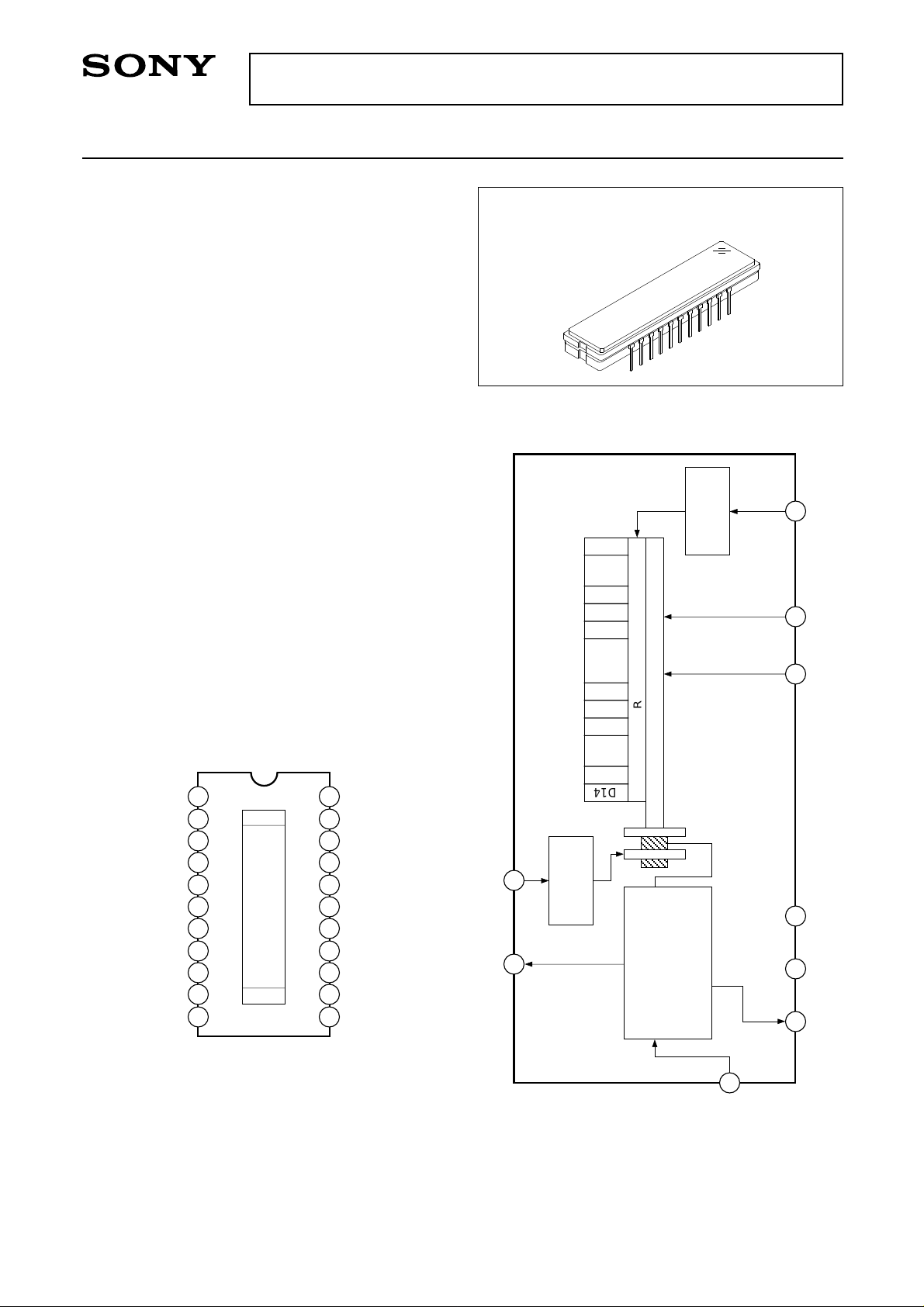
Pin Configuration (Top View)
VOUT
V
SS
NC
φS/H
NC
NC
NC
NC
φ1
NC
φROG
10
11
1
2
3
4
5
6
7
8
9
1
2700
22
21
20
19
18
17
16
15
14
13
12
NC
NC
V
DD
T1
φRS
NC
NC
NC
φ2
NC
NC
Block Diagram
18
φRST1
Timing
19
D39
D34
S2700
S2699
S2
S1
D33
D15
D14
Generator
Timing
Generator
Read Out gate
CCD Analog Shift Register
• Output Amplifier
• Sample-and-Hold Circuit
• Feed Through Level
Clamp Circuit
11
9
14
20
2
1
VDD
GNDVOUT φROGφ1φ2
4
φS/H
Sony reserves the right to change products and specifications without prior notice. This information does not convey any license by
any implication or otherwise under any patents or other right. Application circuits shown, if any, are typical examples illustrating the
operation of the devices. Sony cannot assume responsibility for any problems arising out of the use of these circuits.
– 1 –
E97442A78

Pin Description
Pin No. Symbol Description Pin No. Symbol Description
ILX523A
1
2
3
4
5
6
7
8
9
10
11
VOUT
GND
NC
φS/H
NC
NC
NC
NC
φ1
NC
φROG
Signal output
GND
NC
Sample-and-Hold pulse
NC
NC
NC
NC
Transfer pulse 1
NC
Read out gate pulse
12
13
14
15
16
17
18
19
20
21
22
NC
NC
φ2
NC
NC
NC
φRS
T1
VDD
NC
NC
Note) Connect Pin 4 to GND when not using internal sample-and-hold circuit.
Recommended Pin Voltage
Item
VDD
Min.
11.4
Typ.
12.0
Max.
12.6
Unit
V
NC
NC
Transfer pulse 2
NC
NC
NC
Reset gate pulse
Test pin (Open)
12V power supply
NC
NC
Clock Characteristics
Item
Input capacitance of φ1
Input capacitance of φ2
Input capacitance of φROG
Input capacitance of φRS
Input capacitance of φS/H
Data Rate
Symbol
Cφ1
Cφ2
CφROG
CφRS
CφS/H
—
Min.
—
—
—
—
—
—
Typ.
300
300
10
10
10
1.0
Max.
—
—
—
—
—
5.0
Unit
pF
pF
pF
pF
pF
MHz
– 2 –

Electrooptical Characteristics
(Ta = 25°C, VDD = 12V, data rate = 1MHz, mode without S/H (Pin 4 = GND),
light source = 3200K, IR cut filter CM-500S (t = 1.0mm) used)
Item Symbol Min. Typ. Max. Unit Remarks
ILX523A
Sensitivity
Sencitivity nonuniformity
Saturation output voltage
Dark voltage average
Dark signal nonuniformity
Image Lag
Dynamic range
Saturation exposure
Supply current
Total transfer efficiency
Output impedance
Offset level
Notes)
1. For the sensitivity test, light is applied with a uniform intensity of illumination.
2. PRNU is defined as indicated below. Ray incidence conditions are the same as for Note 1.
The output signal amplitude for test is 1V.
PRNU = × 100 [%]
(VMAX – VMIN)/2
VAVE
R1
PRNU
VSAT
VDRK
DSNU
IL
DR
SE
IVDD
TTE
ZO
VOS
66.5
—
2.0
—
—
—
—
—
—
92.0
—
—
95
2.0
2.5
2.0
7.0
0.02
1250
0.02
15.0
98.0
300
7.4
123.5
10.0
—
8.0
14.0
—
—
—
25.0
—
—
—
V/(lx · s)
%
V
mV
mV
%
—
lx · s
mA
%
Ω
V
Note 1
Note 2
—
Note 3
Note 3
Note 4
Note 5
Note 6
—
—
—
Note 7
The maximum output of all the valid pixels is set to VMAX, the minimum output to VMIN and the average
output to VAVE.
3. Optical signal accumulated time stands at 10ms.
4. Output signal amplitude VOUT = 500mV.
5. Dynamic range is defined as follows.
DR =
When the optical signal accumulated time is shorter, the dynamic range gets wider because the optical
signal accumulated time is in proportion to the dark voltage.
6. Saturation exposure is defined as follows.
SE =
7. VOS is defined as indicated below.
VSAT
VDRK
VSAT
R1
VOUT
D30 D31D29 D33 S1D32
VOS
A
GND
– 3 –

ILX523A
2739
D39
D38
D37
D36
D35
D34
S2700
S2699
S2698
S2697
S4
S3
S2
S1
D33
D32
D31
D15
D14
D13
D12
D11
Dummy signal (6 pixels)
(2700 pixels)
Effective picture elements signal
(18 pixels)
Optical black
1-line output period (2739 pixels)
Note) 2750 or more clock pulses (φ1, φ2, φRS) are required.
234561 21
φROG
0
5
0
5
φ1
0
φ2
5
φRS
5
Clock Timing Diagram (without internal sample-and-hold circuit)
– 4 –
D6
D5
D4
D3
D2
D1
Dummy signal (33 pixels)
0
OUT
V
 Loading...