


5150-pixel CCD Linear Sensor (B/W)
For the availability of this product, please contact the sales office.
Description
The ILX510 is a reduction type CCD linear sensor
developed for high resolution copiers. This sensor
reads A3-size documents at a density of 400 DPI,
and A4-size documents at a density of 600 DPI at
high speed.
Features
• Number of effective pixels: 5150 pixels
• Pixel size: 7 µm×7 µm (7 µm pitch)
• Signal output phase of two-output
simultaneous-output
(alternate-output is available)
• Ultra high sensitivity/Ultra low lag
• Max Data Rate: 40 MHz
• Single 12 V power supply
• Input Clock Pulse: CMOS 5V drive
• Package: 22 pin cer-DIP (400 mil)
Block Diagram
ILX510
20 pin DIP (Cer-DIP)
Absolute Maximum Ratings
• Supply voltage VDD 15 V
• Operating temperature –10 to +60 °C
• Storage temperature –30 to +80 °C
Pin Configuration (TOP VIEW)
22
21
20
19
18
17
16
15
14
13
GND
GND
V
OUT-EVEN
VDD
φRS-EVEN
φLH-EVEN
NC
NC
φ2-EVEN
φ1-EVEN
φROG
NC
1
VGG
2
V
OUT-ODD
3
VDD
4
φRS-ODD
5
φLH-ODD
6
NC
7
GND
8
φ2-ODD
9
φ1-ODD
10
VDD
11 12
1
5150
φRS-EVEN φLH-EVEN φ2-EVEN φ1-EVEN
GND VDD
fROG pulse
D94
1314171821 19
CCD analog shift register
Output amplifer
20
OUT-EVEN
V
Read out gate
22
GND
D75
S5150
S5149
S2
S1
D74
D26
D25
Read out gate
CCD analog shift register
2
VGG
generator
Output amplifer
3
VOUT-ODD
φROG
DD
V
10 11 12
φ1-ODD
φ2-ODD
GND
φLH-ODD φRS-ODD
4 5 6 8 9
VDD
Sony reserves the right to change products and specifications without prior notice. This information does not convey any license by
any implication or otherwise under any patents or other right. Application circuits shown, if any, are typical examples illustrating the
operation of the devices. Sony cannot assume responsibility for any problems arising out of the use of these circuits.
—1—
E94106-TE

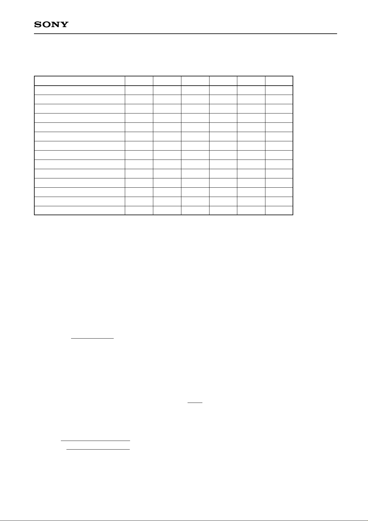
Pin Description
Pin No Symbol Description Pin No Symbol Description
1NCNC 12φROG Readout gate clock pulse input
2VGG Output circuit gate bias 13 φ1-EVEN Clock pulse input (even pixel)
3VOUT-ODD Signal out (odd pixel) 14 φ2-EVEN Clock pulse input (even pixel)
4VDD 12 V power supply 15 NC NC
5 φRS-ODD Clock pulse input (odd pixel) 16 NC NC
6 φLH-ODD Clock pulse input (odd pixel) 17 φLH-EVEN Clock pulse input (even pixel)
7NCNC 18φRS-EVEN Clock pulse input (even pixel)
8 GND GND 19 VDD 12 V power supply
9 φ2-ODD Clock pulse input (odd pixel) 20 VOUT-EVEN Signal out (even pixel)
10 φ1-ODD Clock pulse input (odd pixel) 21 GND GND
11 VDD 12 V power supply 22 GND GND
Recommended Supply Voltage
Item Min. Typ. Max. Unit
VDD 11.4 12 12.6 V
ILX510
Clock Characteristics
Item Symbol Min. Typ. Max. Unit
Input capacity of φ1∗, f2
Input capacity of φLH
Input capacity of φRS
∗
∗
∗
Cφ1, Cφ2 — 400 — pF
CφLH —10—pF
CφRS —10—pF
Input capacity of φROG CφROG —10—pF
∗
It indicates that φ1-ODD, φ1-EVEN as φ1, φ2-ODD, φ2-EVEN as φ2, φLH-ODD, φLH-EVEN as φLH, φRS-ODD, φRS-EVEN
as φRS.
Clock Frequency
Item Symbol Min. Typ. Max. Unit
φ1, φ2, φLH, φRS fφ1, fφ2,fφLH,fφRS — 1 20 MHz
Data rate fφR — 2 40 MHz
Input Clock Pulse Voltage Condition
Item Min. Typ. Max. Unit
φ1, φ2, φLH, φRS, φROG pulse voltage
High level 4.75 5.0 5.25 V
Low level — 0 0.1 V
—2—
Electrooptical Characteristics (Note 1)
(Ta = 25 °C, VDD = 12 V, Data rate fφR=2 MHz, Simultaneous output, Input clock =5 Vp-p
Light source = 3200 K, IR cut filter CM-500S (t = 1.0 mm)
Item Symbol Min. Typ. Max. Unit Remarks
Sensitivity 1 R1 9 12 15 V/(lx•s) Note2
Sensitivity 2 R2 — 27.4 — V/(lx•s) Note3
Sensitivity nonuniformity PRNU — 4 10 % Note4
Saturation output voltage VSAT 1.0 1.5 — V Note5
Saturation exposure SE 0.067 0.125 — lx•s Note6
Register imbalance RI — 2 7 % Note7
Dark voltage average VDRK — 0.3 2.0 mV Note8
Dark signal nonuniformity DSNU — 0.6 3.0 mV Note9
Image lag IL — 0.02 — % Note10
Supply current IVDD —3060mA—
Total transfer efficiency TTE 92 98 — % —
Output impedance ZO — 150 — Ω —
Offset level VOS — 6.5 — V Note11
Dynamic range DR 500 5000 — — Note12
ILX510
Note
1) In accordance with the given electrooptical characteristics, the even black level is defined as the average
value of D6, D8 to D24. The odd black level is defined as the average value of D5, D7 to D23.
2) For the sensitivity test light is applied with a uniform intensity of illumination.
3) W lamp (2854 K).
4) PRNU is defined as indicated below. Ray incidence conditions are the same as for Note 2.
VOUT=500 mV (Typ.)
PRNU =
Where the 5150 pixels are divided into blocks of 103, even and odd pixels, respectively. The maximum
output of each block is set to VMAX, the minimum output to VMIN and the average output to VAVE.
5) Use below the minimum value of the saturation output voltage.
6) Saturation exposure is defined as follows.
(VMAX – VMIN)/2
VAVE
×100 (%)
SE =
VSAT
R1
7) RI is defined as indicated below. VOUT=500 mV (Typ.)
VODD-AVE – VEVEN-AVE
RI =
Where average of odd pixels output is set to VODD-AVE, even pixels to VEVEN-AVE.
VODD-AVE + VEVEN-AVE
(
2
×100 (%)
)
—3—
ILX510
8) Optical signal accumulated time τ int stands at 10 ms.
9) The difference between the maximum and average values of the dark output voltage is calculated for even
and odd respectivery. The larger value is defined as the dark signal nonuniformity.
Optical signal accumulated time t int stands at 10 ms.
10) VOUT = 500 mV (Typ.)
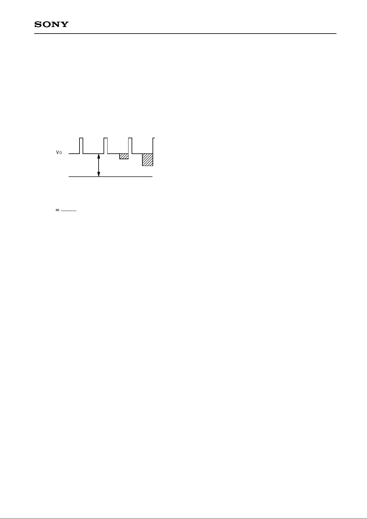
11) Vos is defined as indicated bellow.
VOUT
VOS
GND
12) Dynamic range is defined as follows.
VSAT
DR =
VDRK
When the optical signal accumulated time is shorter, the dynamic range gets wider because the optical
signal accumulated time is in proportion to the dark voltage.
—4—

ILX510
2622
D93
D83
D81
D79
D77
D75
S5149
S5147
S5145
S3
S1
D73
D71
D69
D94
D84
D82
D80
D78
D76
S5150
S5148
S5146
S4
S2
D74
D72
D70
1-line output period (5244 pixels)
D27
D25
D23
5
φROG
3
2
1
5
0
φLH-ODD
φLH-EVEN
5
φ2-ODD
0
EVEN
φ1-ODD
φ1-
0
φ2-EVEN
5
φRS-ODD
0
φRS-EVEN
D5
D3
D1
VOUT-ODD
Clock Timing Chart 1 (simultaneous output)
D28
D26
D24
D6
D4
D2
VOUT-EVEN
Optical black (48 pixels)
Dummy signal (74 pixels)
Note) The transfer pulses (φ1, φ2, φLH) must have more than 2622 cycles.
—5—
 Loading...