

Sony ICX205AK Datasheet
Description
The ICX205AK is a diagonal 8mm (Type 1/2)
interline CCD solid-state image sensor with a square
pixel array and 1.45M effective pixels. Progressive
scan allows all pixels' signals to be output
independently within approximately 1/7.5 second.
Also, the adoption of high frame rate readout mode
supports 30 frames per second. This chip features
an electronic shutter with variable charge-storage
time which makes it possible to realize full-frame still
image without a mechanical shutter. High resolution
and high color reproductivity are achieved through
the use of R, G, B primary color mosaic filters.
Further, high sensitivity and low dark current are
achieved through the adoption of HAD (HoleAccumulation Diode) sensors.
This chip is suitable for applications such as
electronic still cameras, PC input cameras, etc.
Features
• Progressive scan allows individual readout of the
image signals from all pixels.
• High horizontal and vertical resolution (both approx.
800TV-lines) still image without a mechanical shutter.
• Supports high frame rate readout mode
(effective 256 lines output, 30 frame/s)
• Square pixel
• Horizontal drive frequency: 14.318MHz
• No voltage adjustments
(reset gate and substrate bias are not adjusted.)
• R, G, B primary color mosaic filters on chip
• High resolution, high color reproductivity,
high sensitivity, low dark current
• Low smear, excellent antiblooming characteristics
• Continuous variable-speed shutter
Device Structure
• Interline CCD image sensor
• Image size: Diagonal 8mm (Type 1/2)
• Total number of pixels: 1434 (H) × 1050 (V) approx. 1.50M pixels
• Number of effective pixels: 1392 (H) × 1040 (V) approx. 1.45M pixels
• Number of active pixels: 1360 (H) × 1024 (V) approx. 1.40M pixels (7.959mm diagonal)
• Chip size: 7.60mm (H) × 6.20mm (V)
• Unit cell size: 4.65µm (H) × 4.65µm (V)
• Optical black: Horizontal (H) direction: Front 2 pixels, rear 40 pixels
Vertical (V) direction: Front 8 pixels, rear 2 pixels
• Number of dummy bits: Horizontal 20
Vertical 3
• Substrate material: Silicon
Diagonal 8mm (Type 1/2) Progressive Scan CCD Image Sensor with Square Pixel for Color Cameras
– 1 –
E98118B99
Sony reserves the right to change products and specifications without prior notice. This information does not convey any license by
any implication or otherwise under any patents or other right. Application circuits shown, if any, are typical examples illustrating the
operation of the devices. Sony cannot assume responsibility for any problems arising out of the use of these circuits.
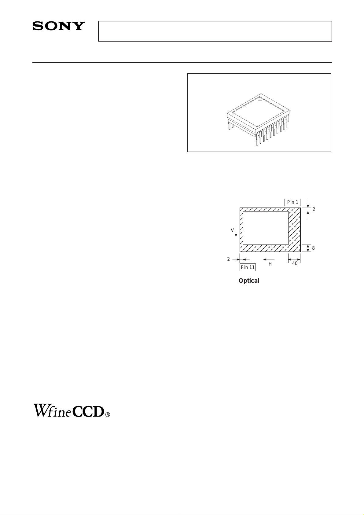
ICX205AK
20 pin DIP (Cer-DIP)
∗
Wfine CCD is a registered trademark of Sony Corporation.
Represents a CCD adopting progressive scan, primary color filter and square pixel.
A
A
A
Pin 1
V
2
40
2
8
Pin 11
H
Optical black position
(Top View)
AAA
AAA
AAA
– 2 –
ICX205AK
Pin No. Symbol Description Pin No. Symbol Description
1
2
3
4
5
6
7
8
9
10
Vφ1
Vφ2A
Vφ2B
Vφ3
NC
NC
GND
NC
GND
VOUT
Vertical register transfer clock
Vertical register transfer clock
Vertical register transfer clock
Vertical register transfer clock
GND
GND
Signal output
11
12
13
14
15
16
17
18
19
20
VDD
GND
φSUB
NC
CSUB
NC
VL
φRG
Hφ1
Hφ2
Supply voltage
GND
Substrate clock
Substrate bias
∗1
Protective transistor bias
Reset gate clock
Horizontal register transfer clock
Horizontal register transfer clock
Pin Description
Note) : Photo sensor
G
R
G
R
G
B
B
G
B
G
Note)
B
B
G
B
G
G
R
G
R
G
Horizontal register
R GG
R
2
3
4
5
6
7
8
9
10
11
12
13
14 15
16
17
18
19
20
1
Vertical register
V
OUT
GND
NC
GND
NC
NC
Vφ
3
Vφ
2B
Vφ
2A
Vφ
1
V
DD
GND
φSUB
NC
C
SUB
NC
V
L
φRG
Hφ
1
Hφ
2
...
...
...
...
Block Diagram and Pin Configuration
(Top View)
∗1
DC bias is generated within the CCD, so that this pin should be grounded externally through a capacitance
of 0.1µF.
– 3 –
ICX205AK
Against φSUB
Against GND
Against VL
Between input
clock pins
Storage temperature
Operating temperature
Absolute Maximum Ratings
–40 to +10
–50 to +15
–50 to +0.3
–40 to +0.3
–25 to
–0.3 to +18
–10 to +18
–10 to +15
–0.3 to +28
–0.3 to +15
to +15
–16 to +16
–16 to +16
–30 to +80
–10 to +60
V
V
V
V
V
V
V
V
V
V
V
V
V
°C
°C
VDD, VOUT, φRG – φSUB
Vφ2A, Vφ2B – φSUB
Vφ1, Vφ3, VL – φSUB
Hφ1, Hφ2, GND – φSUB
CSUB – φSUB
VDD, VOUT, φRG, CSUB – GND
Vφ1, Vφ2A, Vφ2B, Vφ3 – GND
Hφ1, Hφ2 – GND
Vφ2A, Vφ2B – VL
Vφ1, Vφ3, Hφ1, Hφ2, GND – VL
Voltage difference between vertical clock input pins
Hφ1 – Hφ2
Hφ1, Hφ2 – Vφ3
Item Ratings Unit Remarks
∗1
+24V (Max.) when clock width < 10µs, clock duty factor < 0.1%.
+16V (Max.) is guaranteed for turning on or off power supply.
∗1
– 4 –
ICX205AK
Clock Voltage Conditions
Item
Readout clock voltage
VVT
VVH02A
VVH1, VVH2A,
VVH2B, VVH3
VVL1, VVL2A,
VVL2B, VVL3
Vφ1, Vφ2A,
Vφ2B, Vφ3
| VVL1 – VVL3 |
VVHH
VVHL
VVLH
VVLL
VφH
VHL
VφRG
VRGLH – VRGLL
VRGL – VRGLm
VφSUB
14.55
–0.05
–0.2
–8.4
7.6
4.75
–0.05
3.0
22.15
15.0
0
0
–8.0
8.0
5.0
0
3.3
23.0
15.45
0.05
0.05
–7.6
8.4
0.1
0.9
1.3
1.0
0.9
5.25
0.05
5.5
0.4
0.5
23.85
V
V
V
V
V
V
V
V
V
V
V
V
V
V
V
V
1
2
2
2
2
2
2
2
2
2
3
3
4
4
4
5
VVH = VVH02A
VVL = (VVL1 + VVL3)/2
High-level coupling
High-level coupling
Low-level coupling
Low-level coupling
Low-level coupling
Low-level coupling
Horizontal transfer
clock voltage
Reset gate clock
voltage
Substrate clock voltage
Vertical transfer clock
voltage
Symbol Min. Typ. Max. Unit
Waveform
diagram
Remarks
Bias Conditions
Item
Supply voltage
Protective transistor bias
Substrate clock
Reset gate clock
VDD
VL
φSUB
φRG
14.55
15.0
∗1
∗2
∗2
15.45 V
Symbol Min. Typ. Max. Unit Remarks
DC Characteristics
Item
Supply current
IDD
5.5
mA
Symbol Min. Typ. Max. Unit Remarks
∗1
VL setting is the VVL voltage of the vertical transfer clock waveform, or the same power supply as the VL
power supply for the V driver should be used.
∗2
Do not apply a DC bias to the substrate clock and reset gate clock pins, because a DC bias is generated
within the CCD.
– 5 –
ICX205AK
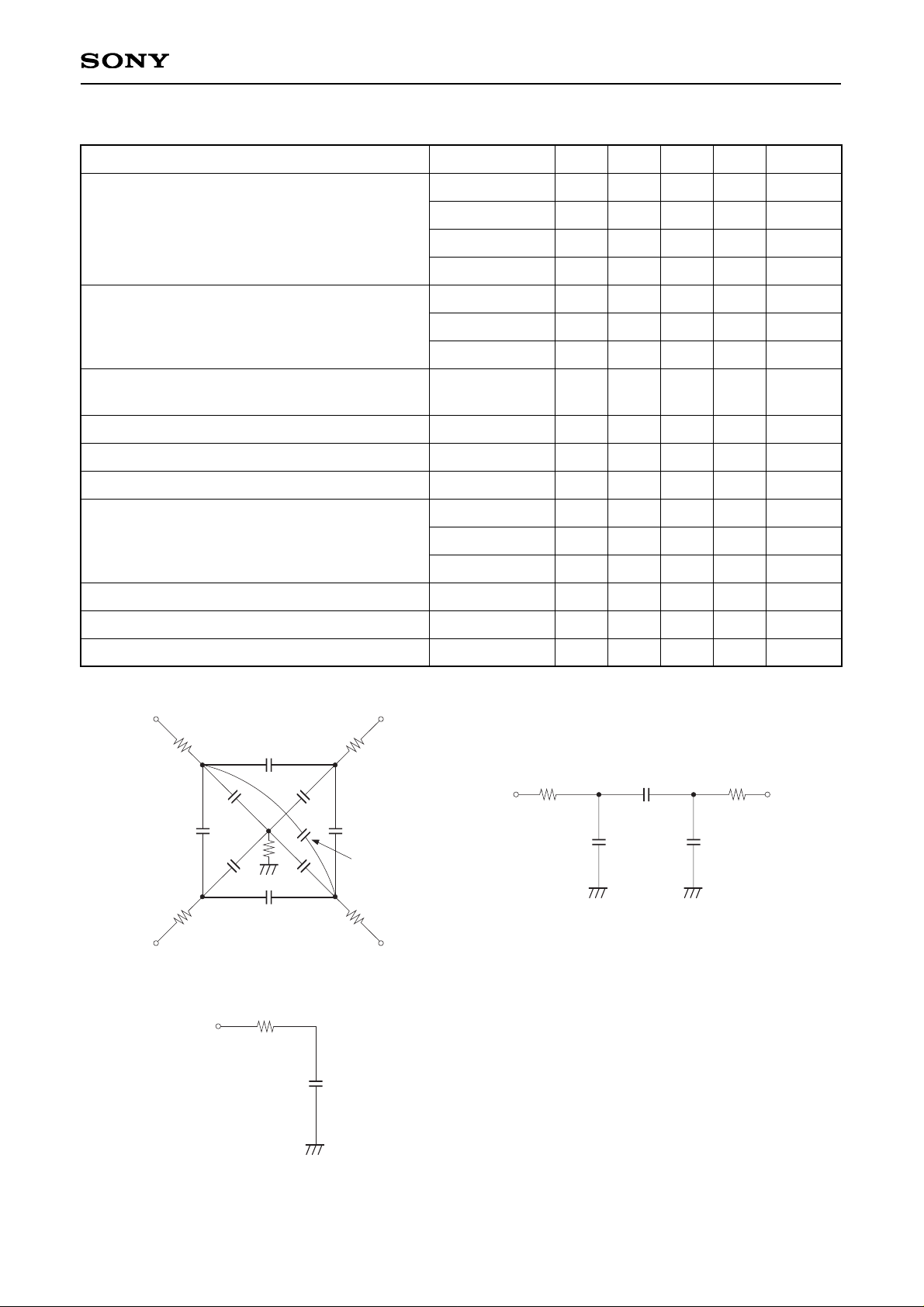
Clock Equivalent Circuit Constant
Item
Capacitance between vertical transfer clock and
GND
CφV1
CφV2A
CφV2B
CφV3
CφV12A, CφV2B1
CφV2A3, CφV32B
CφV13
CφH1, CφH2
CφHH
CφRG
CφSUB
R1
R2A, R3
R2B
RGND
RφH
RφRG
2200
1800
6800
3300
1200
1200
2200
47
100
8
680
36
56
43
30
15
20
pF
pF
pF
pF
pF
pF
pF
pF
pF
pF
pF
Ω
Ω
Ω
Ω
Ω
Ω
Capacitance between vertical transfer clocks
Capacitance between horizontal transfer clock
and GND
Capacitance between horizontal transfer clocks
Capacitance between reset gate clock and GND
Capacitance between substrate clock and GND
Vertical transfer clock series resistor
Vertical transfer clock ground resistor
Horizontal transfer clock series resistor
Reset gate clock series resistor
Symbol Min.
Typ.
Max. Unit Remarks
RφH RφH
Hφ2
Hφ1
CφH1 CφH2
CφHH
Vφ1
CφV12A
Vφ2A
Vφ2B Vφ3
CφV32B
CφV2A3CφV2B1
CφV13
CφV1 CφV2A
CφV2B
CφV3
RGND
R2B
R1
R3
R2A
Vertical transfer clock equivalent circuit Horizontal transfer clock equivalent circuit
RφRG
RGφ
Cφ
RG
Reset gate clock equivalent circuit
– 6 –
ICX205AK
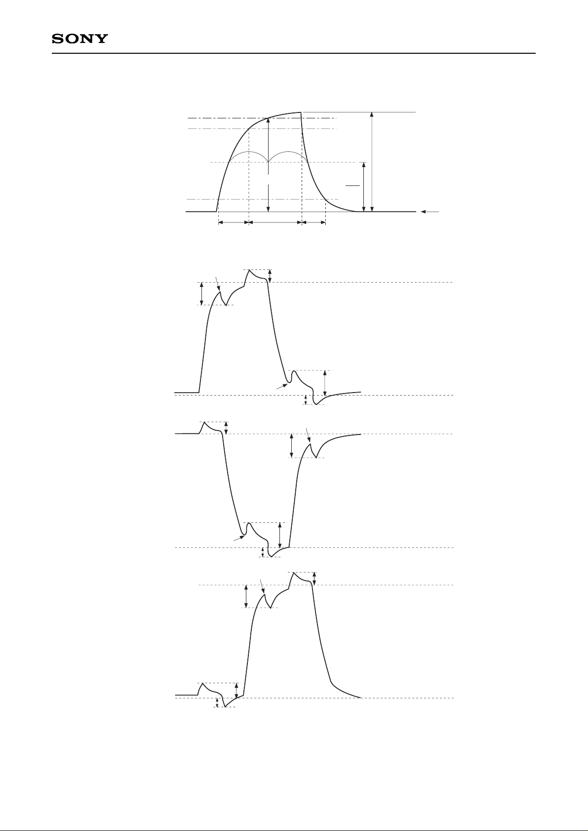
Drive Clock Waveform Conditions
(1) Readout clock waveform
(2) Vertical transfer clock waveform
II II
100%
90%
10%
0%
VVT
tr twh tf
φM
0V
φM
2
Vφ1
Vφ3
Vφ2A, Vφ2B
VVH1
VVHH VVH
VVHL
VVLH
VVL1
VVL01
VVL
VVLL
VVH3
VVHH VVH
VVHL
VVLH
VVL03
VVL
VVLL
VφV1 = VVH1 – VVL01
VφV2A = VVH02A – VVL2A
VφV2B = VVH02B – VVL2B
VφV3 = VVH3 – VVL03
VVH = VVH02A
VVL = (VVL01 + VVL03) / 2
VVL3 = VVL03
VVLH
VVL2A, VVL2B
VVLL
VVL
VVH
VVHH
VVH02A, VVH02B
VVH2A, VVH2B
VVHL
VT
Note) Readout clock is used by composing vertical transfer clocks Vφ2A and Vφ2B.
– 7 –
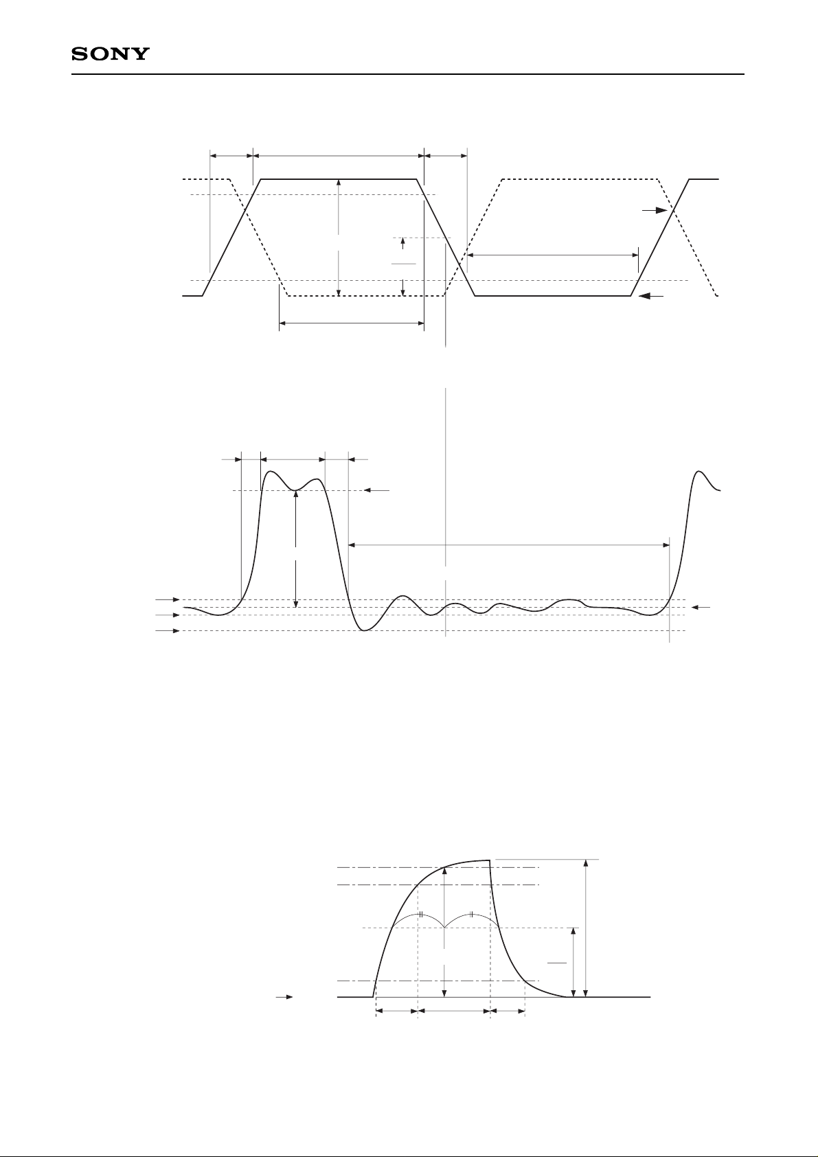
ICX205AK
twh tftr
90%
10%
V
HL
twl
Hφ1
two
Hφ2
VRGL
VRGLL
VRGLH
twl
V
RGH
RG waveform
VRGLm
tr
VφH
2
twh tf
V
CR
Point A
(3) Horizontal transfer clock waveform
(4) Reset gate clock waveform
VφH
VφRG
Cross-point voltage for the Hφ1 rising side of the horizontal transfer clocks Hφ1 and Hφ2 waveforms is VCR.
The overlap period for twh and twl of horizontal transfer clocks Hφ1 and Hφ2 is two.
VRGLH is the maximum value and VRGLL is the minimum value of the coupling waveform during the period from
Point A in the above diagram until the rising edge of RG.
In addition, VRGL is the average value of VRGLH and VRGLL.
VRGL = (VRGLH + VRGLL)/2
Assuming VRGH is the minimum value during the interval twh, then:
VφRG = VRGH – VRGL.
Negative overshoot level during the falling edge of RG is VRGLm.
(5) Substrate clock waveform
90%
100%
10%
0%
V
SUB
(A bias generated within the CCD)
tr twh tf
φM
φM
2
VφSUB
 Loading...