

Sony ICX080AK Datasheet
– 1 –
ICX080AK
E95518D99
Diagonal 6mm (Type 1/3) CCD Image Sensor for NTSC Color Video Cameras
Description
The ICX080AK is an interline CCD solid-state
image sensor suitable for NTSC color video
cameras. This chip conforms to DV standard SD
mode, and has the optimal number of pixels for
MPEG2 Main level. While achieving a horizontal
resolution of 450 TV lines, the area has been
expanded 33% in both vertical and horizontal
directions, making the chip suitable for electronic
vibration stabilizer and electronic panning/tilting. In
addition, complete 16:9 wide aspect ratio images
are provided with a high picture quality without
requiring vertical interpolation.
High sensitivity and low dark current are achieved
through the adoption of Ye, Cy, Mg and G
complementary color mosaic filters and HAD (HoleAccumulation Diode) sensors.
This chip features a field period readout system
and an electronic shutter with variable chargestorage time.
The package is a 16-pin DIP (Plastic), and both
top and bottom surface reference can be assured at
the same time.
Features
• Supports electronic vibration stabilizer and electronic panning/tilting
(33%/one side)
• Supports electronic zoom
• Supports DV standard SD mode and MPEG2 Main level (13.5MHz)
• Supports 16:9 wide aspect ratio (for both 18MHz and 5fsc)
• Supply voltage: 12V
• Horizontal register and reset gate: 2.7 to 3.6V drive
• No voltage adjustment (Reset gate and substrate bias are not adjusted.)
• High resolution, high sensitivity, low dark current and low smear
• Excellent antiblooming characteristics
• Continuous variable-speed shutter (1/60 to 1/10000s)
• Supports short exit pupil distance (Recommended range: –20 to –100mm)
• Ye, Cy, Mg and G complementary color mosaic filters on chip
• 16-pin high precision plastic package (both top and bottom surface reference possible)
Device Structure
• Interline CCD image sensor
• Image size: Diagonal 6mm (Type 1/3)
• Total number of pixels: 1016 (H) x 674 (V) approx. 680K pixels
• Total number of effective pixels: 962 (H) x 654 (V) approx. 630K pixels
• Number of effective pixels: 4:3 NTSC: 711 (H) x 485 (V) approx. 340K pixels
16:9 18MHz: 948 (H) x 485 (V) approx. 460K pixels
16:9 5fsc: 942 (H) x 485 (V) approx. 460K pixels
• Chip size: 5.90mm (H) x 4.92mm (V)
• Unit cell size: 5.05µm (H) x 5.55µm (V)
• Optical black: Horizontal (H) direction: Front 4 pixels, rear 50 pixels
Vertical (V) direction: Front 12 pixels, rear 8 pixels
• Number of dummy bits: Horizontal 28
Vertical 1 (even fields only)
• Substrate material: Silicon
Sony reserves the right to change products and specifications without prior notice. This information does not convey any license by
any implication or otherwise under any patents or other right. Application circuits shown, if any, are typical examples illustrating the
operation of the devices. Sony cannot assume responsibility for any problems arising out of the use of these circuits.
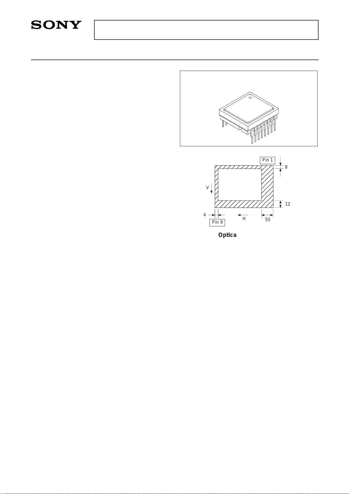
16 pin DIP (Plastic)
A
A
Pin 1
V
4
50
8
12
Pin 9
H
Optical black position
(Top View)
AAAA
AAAA
– 2 –
ICX080AK
Against φSUB
Against GND
Against VL
Between input clock
pins
Storage temperature
Operating temperature
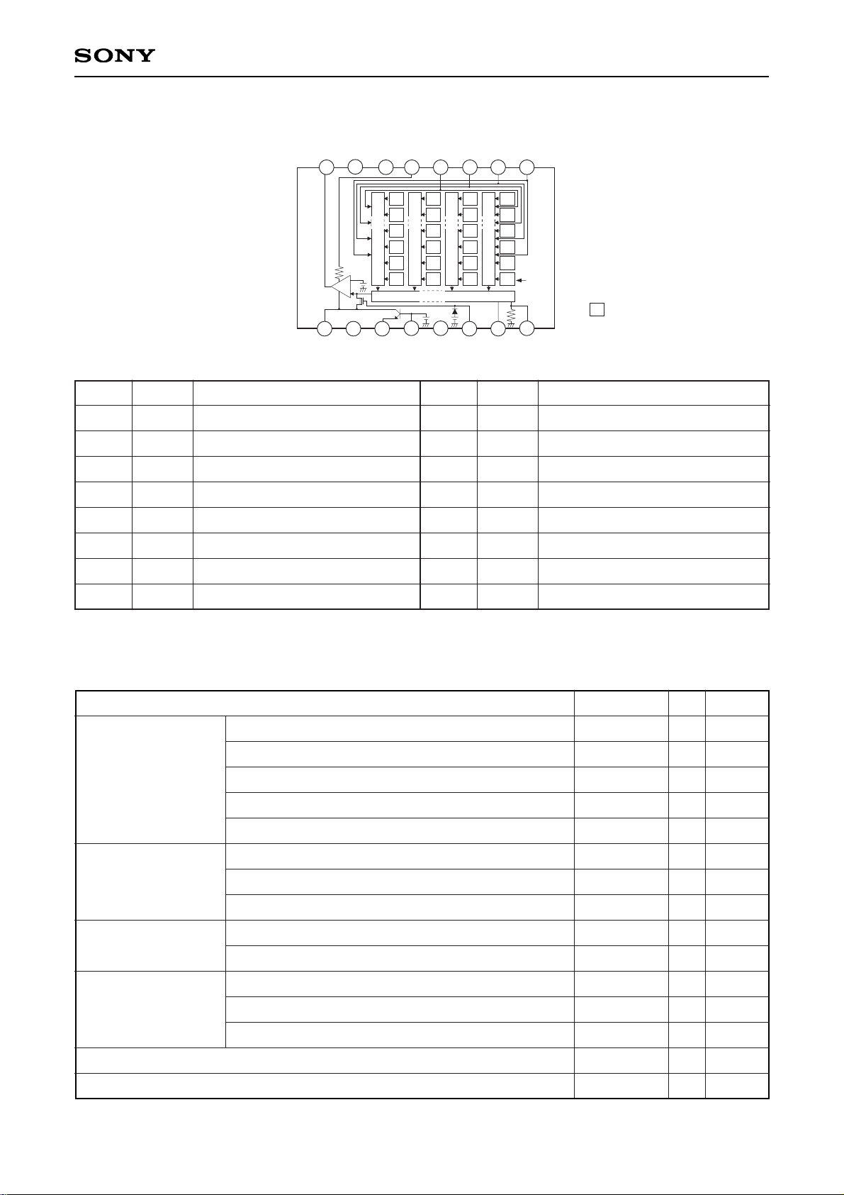
Block Diagram and Pin Configuration
(Top View)
Note) : Photo sensor
V
OUT
GND
GND
GND
Vφ
1
Vφ
2
Vφ
3
Vφ
4
V
DD
GND
φSUB
C
SUB
V
L
φRG
Hφ
1
Hφ
2
Ye
G
Ye
Mg
Ye
G
Cy
Mg
Cy
G
Cy
Mg
Ye
G
Ye
Mg
Ye
G
Cy
Mg
Cy
G
Cy
Mg
Horizontal Register
Note)
Vertical Register
1
2
3
4
5
6
7
8
9
10
11
12
13
14 15
16
Pin No.
1
2
3
4
5
6
7
8
Vφ4
Vφ3
Vφ2
Vφ1
GND
GND
GND
VOUT
Vertical register transfer clock
Vertical register transfer clock
Vertical register transfer clock
Vertical register transfer clock
GND
GND
GND
Signal output
9
10
11
12
13
14
15
16
VDD
GND
φSUB
CSUB
VL
φRG
Hφ1
Hφ2
Supply voltage
GND
Substrate clock
Substrate bias
∗1
Protective transistor bias
Reset gate clock
Horizontal register transfer clock
Horizontal register transfer clock
Symbol Description
Pin Description
Absolute Maximum Ratings
–40 to +10
–50 to +15
–50 to +0.3
–40 to +0.3
–25 to
–0.3 to +18
–10 to +18
–10 to +5
–0.3 to +28
–0.3 to +15
to +15
–5 to +5
–13 to +13
–30 to +80
–10 to +60
V
V
V
V
V
V
V
V
V
V
V
V
V
°C
°C
VDD, VOUT, φRG – φSUB
Vφ1, Vφ3 – φSUB
Vφ2, Vφ4, VL – φSUB
Hφ1, Hφ2, GND – φSUB
CSUB – φSUB
VDD, VOUT, φRG, CSUB – GND
Vφ1, Vφ2, Vφ3, Vφ4 – GND
Hφ1, Hφ2 – GND
Vφ1, Vφ3 – VL
Vφ2, Vφ4, Hφ1, Hφ2, GND – VL
Voltage difference between vertical clock input pins
Hφ1 – Hφ2
Hφ1, Hφ2 – Vφ4
Item Ratings Unit Remarks
∗2
+24V (Max.) when clock width < 10µs, clock duty factor < 0.1%.
∗1
DC bias is generated within the CCD, so that this pin should be grounded externally through a capacitance
of 0.1µF.
∗2
Pin No. Symbol Description
– 3 –
ICX080AK
Clock Voltage Conditions
Item
Readout clock voltage
VVT
VVH1, VVH2
VVH3, VVH4
VVL1, VVL2,
VVL3, VVL4
VφV
VVH3 – VVH
VVH4 – VVH
VVHH
VVHL
VVLH
VVLL
VφH
VHL
VCR
VφRG
VRGLH – VRGLL
VRGL – VRGLm
VφSUB
11.64
–0.05
–0.2
–6.85
5.95
–0.25
–0.25
2.7
–0.05
0.5
2.7
17.3
12.0
0
0
–6.5
6.5
3.3
0
1.65
3.3
18.5
12.36
0.05
0.05
–6.15
6.9
0.1
0.1
0.5
0.5
0.5
0.5
3.6
0.05
3.6
0.4
0.5
19.3
V
V
V
V
V
V
V
V
V
V
V
V
V
V
V
V
V
V
1
2
2
2
2
2
2
2
2
2
2
3
3
3
4
4
4
5
VVH = (VVH1 + VVH2)/2
VVL = (VVL3 + VVL4)/2
VφV = VVHn – VVLn (n = 1 to 4)
High-level coupling
High-level coupling
Low-level coupling
Low-level coupling
Cross-point voltage
Low-level coupling
Low-level coupling
Horizontal transfer
clock voltage
Reset gate clock
voltage
Substrate clock voltage
Vertical transfer clock
voltage
Symbol Min. Typ. Max. Unit
Waveform
diagram
Remarks
Bias Conditions
Item
Supply voltage
Protective transistor bias
Substrate clock
Reset gate clock
VDD
VL
φSUB
φRG
11.64
12.0
∗1
∗2
∗2
12.36
V
Symbol Min. Typ. Max. Unit Remarks
DC Characteristics
Item
Supply current IDD 6.0 mA
Symbol Min. Typ. Max. Unit Remarks
∗1
VL setting is the VVL voltage of the vertical transfer clock waveform, or the same power supply as the VL
power supply for the V driver should be used.
∗2
Do not apply a DC bias to the substrate clock and reset gate clock pins, because a DC bias is generated
within the CCD.
– 4 –
ICX080AK
Clock Equivalent Circuit Constant
Item
Capacitance between vertical transfer clock and
GND
CφV1, CφV3
CφV2, CφV4
CφV12, CφV34
CφV23, CφV41
CφV13
CφV24
CφH1, CφH2
CφHH
CφRG
CφSUB
R1, R2, R3, R4
RGND
RφH
RH2
1000
560
470
390
180
100
62
62
12
270
82
15
3
30
pF
pF
pF
pF
pF
pF
pF
pF
pF
pF
Ω
Ω
Ω
kΩ
Capacitance between vertical transfer clocks
Capacitance between horizontal transfer clock and GND
Capacitance between horizontal transfer clocks
Capacitance between reset gate clock and GND
Capacitance between substrate clock and GND
Vertical transfer clock series resistor
Vertical transfer clock ground resistor
Horizontal transfer clock series resistor
Horizontal transfer clock ground resistor
Symbol Min. Typ. Max. Unit Remarks
RφH RφH
Hφ2Hφ1
CφH1 CφH2
CφHH
Vφ1
CφV12
Vφ2
Vφ4 Vφ3
CφV34
CφV23CφV41
CφV13
CφV24
CφV1 CφV2
CφV4 CφV3
RGND
R4
R1
R3
R2
Vertical transfer clock equivalent circuit Horizontal transfer clock equivalent circuit
RH2
– 5 –
ICX080AK
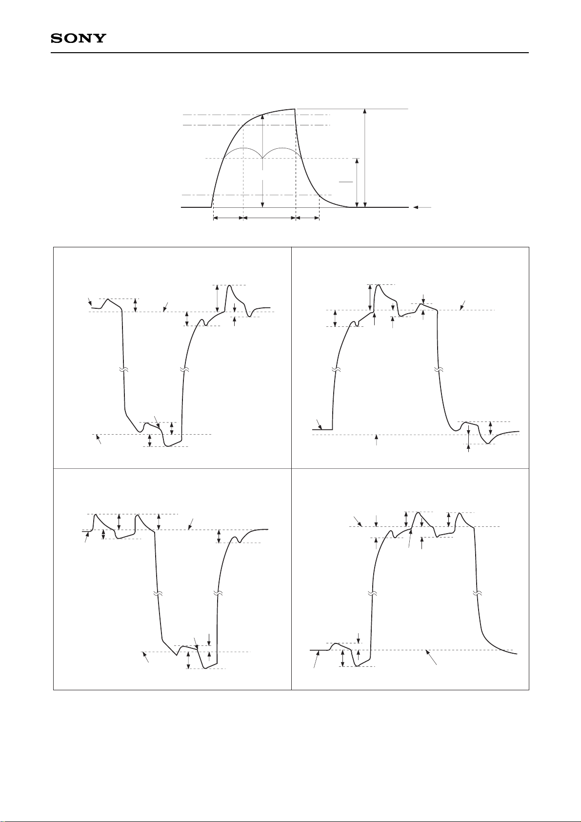
Drive Clock Waveform Conditions
(1) Readout clock waveform
(2) Vertical transfer clock waveform
II II
100%
90%
10%
0%
VVT
tr twh tf
φM
0V
φM
2
Vφ1 Vφ3
Vφ2 Vφ4
VVHH
VVH
VVHL
VVHH
VVHL
VVH1
VVL1
VVLH
VVLL
VVL
VVHH
VVH3
VVHL
VVH
VVHH
VVHL
VVL3
VVL
VVLL
VVLH
VVHH VVHH
VVH
VVHL
VVHL
VVH2
VVLH
VVL2
VVLL
VVL
VVHH VVHH
VVHL
VVH4
VVHL
VVH
VVL
VVLH
VVLL
VVL4
VVH = (VVH1 + VVH2)/2
VVL = (VVL3 + VVL4)/2
VφV = VVHn – VVLn (n = 1 to 4)
– 6 –
ICX080AK
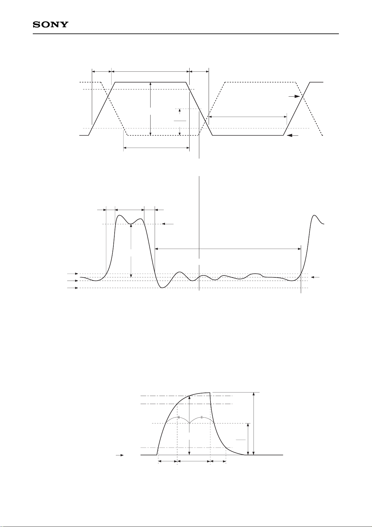
twh tftr
90%
10%
V
HL
twl
Hφ1
two
Hφ2
VRGL
VRGLL
VRGLH
twl
V
RGH
RG waveform
VRGLm
tr twh tf
V
CR
Point A
(3) Horizontal transfer clock waveform
Cross-point voltage for the Hφ1 rising side of the horizontal transfer clocks Hφ1 and Hφ2 waveforms is VCR.
The overlap period for twh and twl of horizontal transfer clocks Hφ1 and Hφ2 is two.
(4) Reset gate clock waveform
VφH
VφH
2
VφRG
VRGLH is the maximum value and VRGLL is the minimum value of the coupling waveform during the period from
Point A in the above diagram until the rising edge of RG. In addition, VRGL is the average value of VRGLH and
VRGLL.
VRGL = (VRGLH + VRGLL) /2
Assuming VRGH is the minimum value during the interval twh, then:
VφRG = VRGH – VRGL.
Negative overshoot level during the falling edge of RG is VRGLm.
(5) Substrate clock waveform
90%
100%
10%
0%
V
SUB
tr twh tf
φM
φM
2
(A bias generated within the CCD)
VφSUB
 Loading...