

Sony ICX076AK Datasheet
Description
The ICX076AK is an interline CCD solid-state
image sensor suitable for NTSC color video
cameras. This device possesses a number of pixels
that is compatible with SIF, and offers excellent cost
performance due to the adoption of an ultra-small
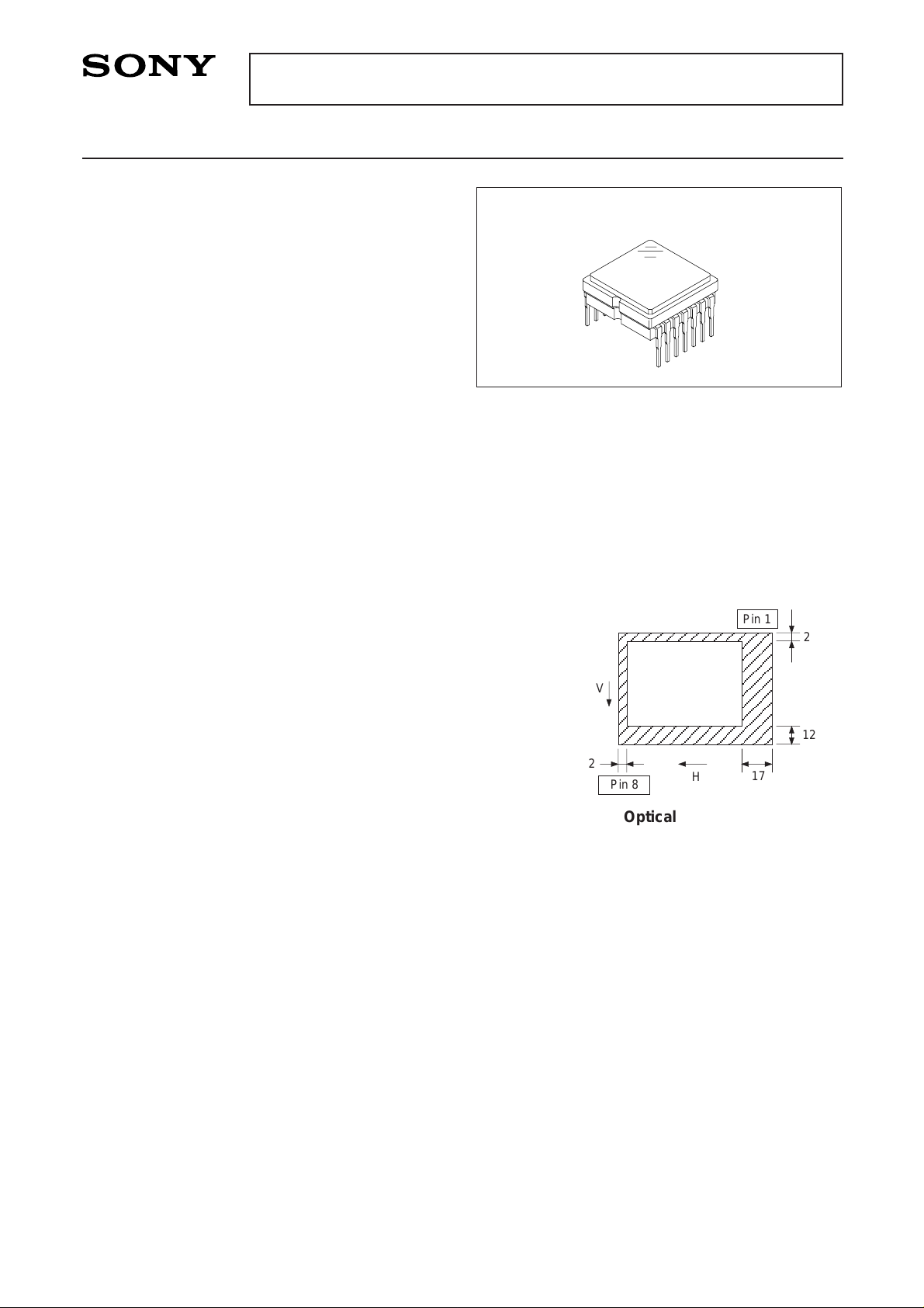
image size and a 10 mm-square 14-pin plastic
package. High sensitivity and low dark current are
achieved through the use of Ye, Cy, Mg, and G
complementary color mosaic filters and through the
adoption of HAD (Hole-Accumulation Diode) sensors.
This chip features a field period readout system
and an electronic shutter with variable chargestorage time.
Features
• High sensitivity and low dark current
• Low smear
• Excellent antiblooming characteristics
• Ye, Cy, Mg, and G complementary color mosaic filters on chip
• Horizontal register: 5V drive (drive frequency: 6.75MHz)
• Reset gate: 5V drive (no adjustment of bias)
Device Structure
• Image size: Diagonal 3.6mm (Type 1/5)
• Number of effective pixels: 362 (H) × 492 (V) approx. 180K pixels
• Total number of pixels: 381 (H) × 506 (V) approx. 190K pixels
• Interline CCD image sensor
• Chip size: 3.75mm (H) × 3.30mm (V)
• Unit cell size: 8.10µm (H) × 4.45µm (V)
• Optical black: Horizontal (H) direction: Front 2 pixels, rear 17 pixels
Vertical (V) direction: Front 12 pixels, rear 2 pixels
• Number of dummy bits: Horizontal 14
Vertical 1 (even fields only)
• Substrate material: Silicon
– 1 –
ICX076AK
E95506D99
Diagonal 3.6mm (Type 1/5) CCD Image Sensor for NTSC Color Video Cameras
Sony reserves the right to change products and specifications without prior notice. This information does not convey any license by
any implication or otherwise under any patents or other right. Application circuits shown, if any, are typical examples illustrating the
operation of the devices. Sony cannot assume responsibility for any problems arising out of the use of these circuits.
A
A
A
Optical black position
(Top View)
14 pin DIP (Plastic)
V
2
Pin 8
AAA
AAA
AAA
H
Pin 1
2
12
17
– 2 –
ICX076AK
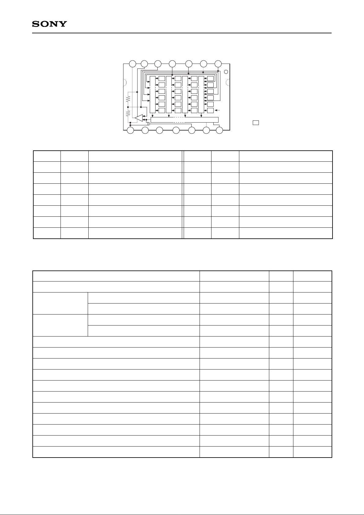
Symbol Description Pin No. Symbol Description
1
2
3
4
5
6
7
Vφ4
Vφ3
Vφ2
Vφ1
CGG
GND
VOUT
Vertical register transfer clock
Vertical register transfer clock
Vertical register transfer clock
Vertical register transfer clock
Output amplifier gate
∗1
GND
Signal output
8
9
10
11
12
13
14
VDD
GND
SUB
VL
RG
Hφ1
Hφ2
Supply voltage
GND
Substrate (overflow drain)
Protective transistor bias
Reset gate clock
Horizontal register transfer clock
Horizontal register transfer clock
: Photo sensor
Note)
V
OUT
GND
SUB
GND
Vφ
1
Vφ
4
Vφ
3
Vφ
2
V
DD
RG
Hφ
1
Hφ
2
Vertical register
Horizontal register
Note)
C
GG
V
L
2
3
4
5
6
7
8
9
10
11
12
13
14
1
Cy
G
Cy
G
Cy
Mg
Ye
Mg
Ye
Mg
Ye
G
Cy
G
Cy
G
Cy
Mg
Ye
Mg
Ye
Mg
Ye
G
Block Diagram and Pin Configuration
(Top View)
Item
–0.3 to +55
–0.3 to +18
–55 to +12
–15 to +20
to +12
to +15
to +17
–17 to +17
–10 to +15
–55 to +10
–65 to +0.3
–0.3 to +27.5
–0.3 to +22.5
–0.3 to +17.5
–30 to +80
–10 to +60
V
V
V
V
V
V
V
V
V
V
V
V
V
V
°C
°C
∗2
∗3
Ratings Unit Remarks
Absolute Maximum Ratings
∗2
+27V (Max.) when clock width < 10µs, clock duty factor < 0.1%.
∗3
When CGG or GND (Pin 6) are grounded.
–0.3 to + 17.5V when CGG and GND (Pin 6) are to be disconnected.
Substrate voltage SUB – GND
Supply voltage
Clock input
voltage
Voltage difference between vertical clock input pins
Voltage difference between horizontal clock input pins
Hφ1, Hφ2 – Vφ4
Hφ1, Hφ2 – GND
Hφ1, Hφ2 – SUB
VL – SUB
Vφ1, Vφ3, VDD, VOUT – VL
RG – GND
Vφ2, Vφ4, CGG, Hφ1, Hφ2, GND – VL
Storage temperature
Operating temperature
VDD, VOUT, CGG – GND
VDD, VOUT, CGG – SUB
V
φ
1, Vφ2, Vφ3, V
φ4–
GND
V
φ
1, Vφ2, Vφ3, V
φ4–
SUB
Pin Description
∗1
DC bias is applied within the CCD, so that this pin should be grounded externally through a capacitance of
1µF or more.
Pin No.
– 3 –
ICX076AK
Item
VDD
VSUB
VL
14.25
5.0
Indicated
voltage – 0.1
15.0
Indicated
voltage
15.75
12.75
Indicated
voltage + 0.1
V
V
V
∗1
Symbol Min. Typ. Max. Unit Remarks
Bias Conditions
∗2
Supply voltage
Substrate voltage adjustment range
Substrate voltage adjustment precision
Protective transistor bias
∗1
Indications of substrate voltage (VSUB) setting value
The setting value of the substrate voltage is indicated on the back of image sensor by a special code.
Adjust the substrate voltage (VSUB) to the indicated voltage.
VSUB code – one character indication
↑
VSUB code
Code and optimal setting correspond to each other as follows.
DC Characteristics
–
VSUB code
5.0
=
5.25
0
5.5
1
5.75
2
6.0
3
6.25
4
6.5
6
6.75
7
7.0
8
7.25
9
7.5
A
7.75
C
8.0
d
8.25
E
VSUB code
8.5
f
8.75
G
9.0h9.25
J
9.5
K
9.75
L
10.0
m
10.25
N
10.5
P
10.75
R
11.0
S
11.25
U
11.5
V
11.75
W
VSUB code
12.0X12.25Y12.5Z12.75
<Example> “L” → VSUB = 10.0V
∗2
VL setting is the VVL voltage of the vertical transfer clock waveform, or the same power supply as the VL
power supply for the V driver should be used.
∗3
1) Current to each pin when 16V is applied to VDD, VOUT, RG, CGG, GND (Pin 6), and SUB pins, while pins
that are not tested are grounded.
2) Current to each pin when 20V is applied sequentially to Vφ1, Vφ2, Vφ3, and Vφ4 pins, while pins that are
not tested are grounded. However, 20V is applied to SUB pin.
3) Current to each pin when 15V is applied sequentially to Hφ1 and Hφ2 pins, while pins that are not tested
are grounded. However, 15V is applied to SUB pin.
4) Current to VL pin when 25V is applied to Vφ1, Vφ 3, VDD, and VOUT pins or when, 15V is applied to Vφ2,
Vφ4, Hφ1, and Hφ2 pins, while VL pin is grounded. However, GND and SUB pins are left open.
5) Current to GND pin when 20V is applied to the RG pin and the GND pin is grounded.
∗4
Current to SUB pin when 55V is applied to SUB pin, while all pins that are not tested are grounded.
Item
Supply current
Input current
Input current
IDD
IIN1
IIN2
3 5
1
10
mA
µA
µA
∗3
∗4
Symbol Min. Typ. Max. Unit Remarks
Optimal setting
Optimal setting
Optimal setting
– 4 –
ICX076AK
Item
Readout clock voltage
VVT
VVH1, VVH2
VVH3, VVH4
VVL1, VVL2,
VVL3, VVL4
VφV
VVH3 – VVH
VVH4 – VVH
VVHH
VVHL
VVLH
VVLL
VφH
VHL
VφRG
VRGLH– VRGLL
VRGH
VφSUB
14.25
–0.05
–0.2
–8.5
7.3
–0.25
–0.25
4.75
–0.05
4.5
VDD + 0.3
21.25
15.0
0
0
–8.0
8.0
5.0
0
5.0
VDD + 0.6
22.5
15.75
0.05
0.05
–7.5
8.55
0.1
0.1
0.3
0.3
0.3
0.3
5.25
0.05
5.5
0.8
VDD + 0.9
23.75
V
V
V
V
V
V
V
V
V
V
V
V
V
V
V
V
V
1
2
2
2
2
2
2
2
2
2
2
3
3
4
4
4
5
VVH = (VVH1 + VVH2)/2
VVL = (VVL3 + VVL4)/2
VφV = VVHn – VVLn
(n = 1 to 4)
High-level coupling
High-level coupling
Low-level coupling
Low-level coupling
Input through 0.01µF
capacitance
Low-level coupling
Horizontal transfer
clock voltage
Reset gate clock
voltage
Substrate clock voltage
Vertical transfer clock
voltage
Symbol Min.
Typ. Max.
Unit
Waveform
diagram
Remarks
Clock Voltage Conditions
– 5 –
ICX076AK
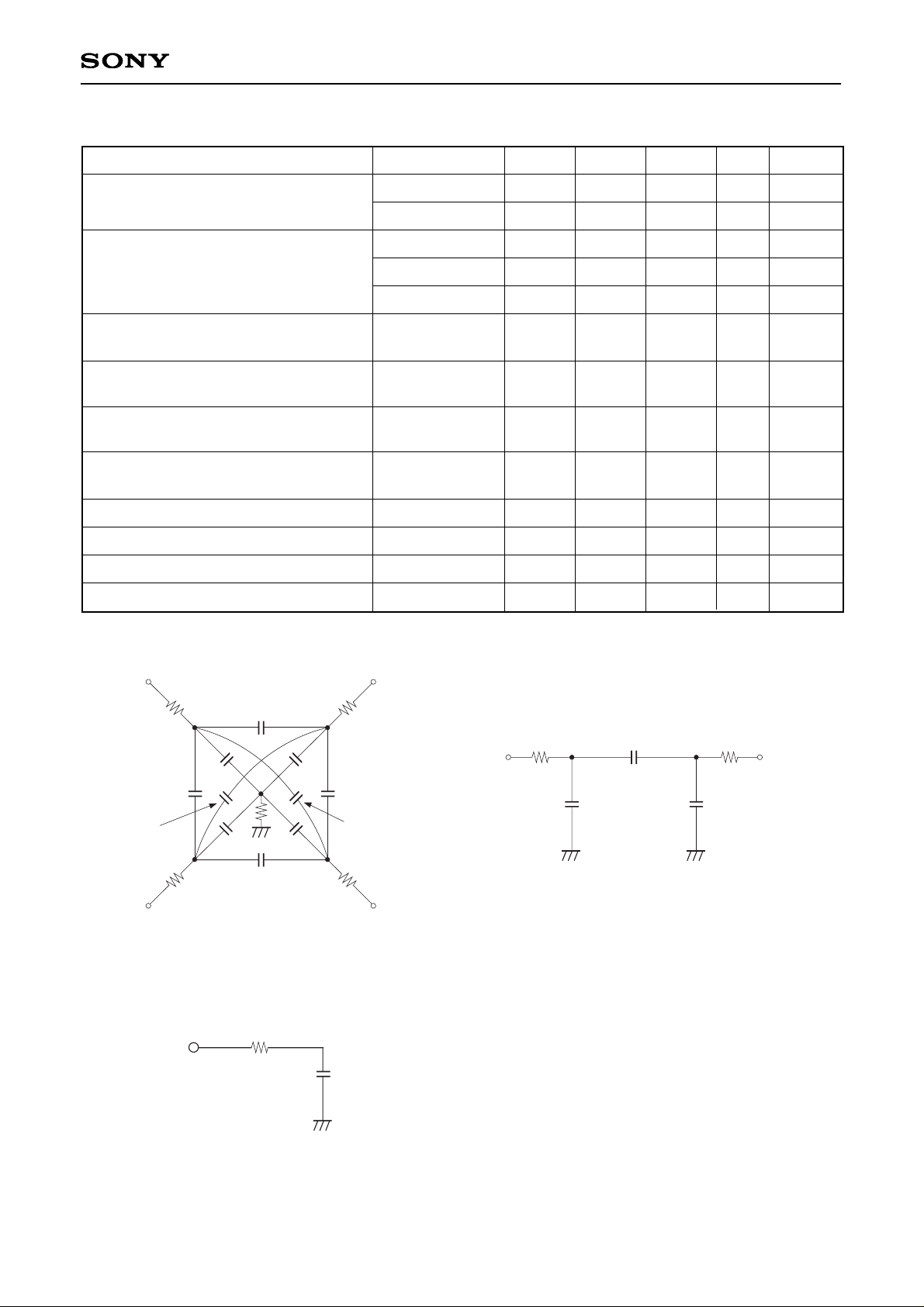
Clock Equivalent Circuit Constant
Item
Capacitance between vertical transfer
clock and GND
CφV1, CφV3
CφV2, CφV4
CφV12, CφV34
CφV23, CφV41
CφV13, CφV24
CφH1, CφH2
CφHH
CφRG
CφSUB
R1, R2, R3, R4
RGND
RφH
RφRG
520
390
220
150
39
24
18
3
170
100
15
30
39
pF
pF
pF
pF
pF
pF
pF
pF
pF
Ω
Ω
Ω
Ω
Capacitance between vertical transfer
clocks
Capacitance between horizontal
transfer clock and GND
Capacitance between horizontal
transfer clocks
Capacitance between reset gate clock
and GND
Capacitance between substrate clock
and GND
Vertical transfer clock series resistor
Vertical transfer clock ground resistor
Horizontal transfer clock series resistor
Reset gate clock series resistor
Symbol
Min. Typ. Max. Unit Remarks
RφH RφH
Hφ2Hφ1
CφH1 CφH2
CφHH
Vφ1
CφV12
Vφ2
Vφ4 Vφ3
CφV34
CφV23
CφV41
CφV13
CφV24
CφV1 CφV2
CφV4 CφV3
RGND
R4
R1
R3
R2
Vertical transfer clock equivalent circuit Horizontal transfer clock equivalent circuit
Reset gate clock equivalent circuit
CφRG
RGφ
Rφ
RG
– 6 –
ICX076AK
Drive Clock Waveform Conditions
(1) Readout clock waveform
(2) Vertical transfer clock waveform
II II
100%
90%
10%
0%
VVT
tr twh tf
φM
0V
φM
2
Vφ1 Vφ3
Vφ2 Vφ4
VVHH
VVH
VVHL
VVHH
VVHL
VVH1
VVL1
VVLH
VVLL
VVL
VVHH
VVH3
VVHL
VVH
VVHH
VVHL
VVL3
VVL
VVLL
VVLH
VVHH VVHH
VVH
VVHL
VVHL
VVH2
VVLH
VVL2
VVLL
VVL
VVHH VVHH
VVHL
VVH4
VVHL
VVH
VVL
VVLH
VVLL
VVL4
VVH = (VVH1 + VVH2)/2
VVL = (VVL3 + VVL4)/2
VφV = VVHn – VVLn (n = 1 to 4)
 Loading...