

Sony ICX074AL Datasheet
Description
The ICX074AL is an interline CCD solid-state
image sensor suitable for EIA black-and-white video
cameras. Progressive scan allows all pixels signals
to be output independently within approximately
1/60 second. This chip features an electronic shutter
with variable charge-storage time which makes it
possible to realize full-frame still image without
mechanical shutter. Individual pixels in a square
matrix make this device suitable for image input and
processing applications.
High sensitivity and low dark current are achieved
through the adoption of HAD (Hole-Accumulation
Diode) sensors.
Features
• Progressive scan allows individual readout of the
image signals from all pixels.
• High vertical resolution (480TV-lines) still picture
without mechanical shutter.
• Square pixel unit cell
• VGA format-compatible
• High resolution, high sensitivity, low dark current
• Continuous variable-speed shutter
• Low smear
• Excellent antiblooming characteristics
• Reset gate: 5V drive (bias: no adjustment)
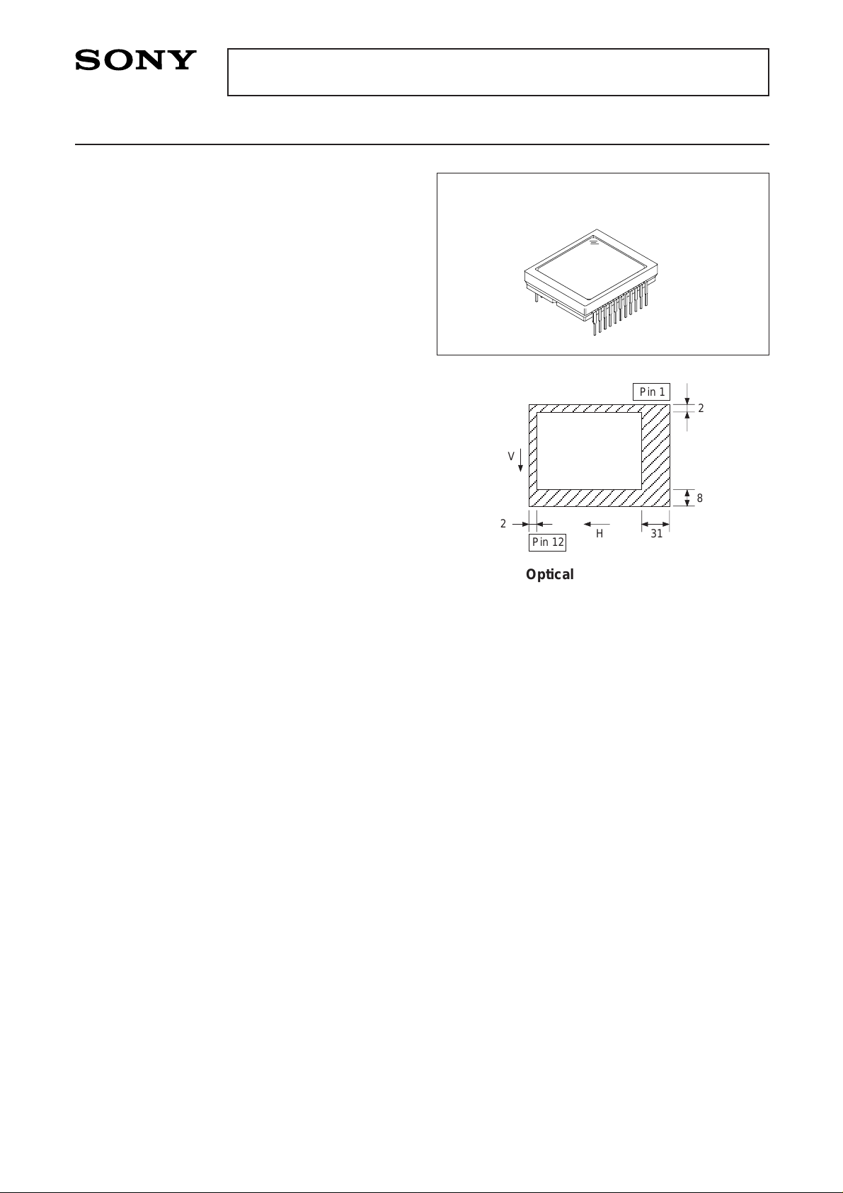
Device Structure
• Image size: Diagonal 8mm (Type 1/2)
• Number of effective pixels: 659 (H) × 494 (V) approx. 330K pixels
• Total number of pixels: 692 (H) × 504 (V) approx. 350K pixels
• Interline CCD image sensor
• Chip size: 8.10mm (H) × 6.33mm (V)
• Unit cell size: 9.9µm (H) × 9.9µm (V)
• Optical black: Horizontal (H) direction: Front 2pixels, rear 31pixels
Vertical (V) direction: Front 8pixels, rear 2pixels
• Number of dummy bits: Horizontal 16
Vertical 5
• Substrate material: Silicon
– 1 –
ICX074AL
E94478H99
Diagonal 8mm (Type 1/2) Progressive Scan CCD Image Sensor with Square Pixel for EIA B/W Video Cameras
Sony reserves the right to change products and specifications without prior notice. This information does not convey any license by
any implication or otherwise under any patents or other right. Application circuits shown, if any, are typical examples illustrating the
operation of the devices. Sony cannot assume responsibility for any problems arising out of the use of these circuits.
22 pin DIP (Cer-DIP)
A
A
A
Pin 1
V
2
31
2
8
Pin 12
H
Optical black position
(Top View)
AAA
AAA
AAA
– 2 –
ICX074AL
Horizontal Register 1
Horizontal Register 2
1
2
3
4
5
6
7
8
9
10
11
12
13
14
Note)
Note) : Photo sensor
V
OUT2
GND
C
GG2
C
GG1
VHOLDφ
Vφ
1
Vφ
2
HIGφ
1
V
DD
VOGφ
SUB
V
L
RG
POGφ
Hφ
1
Hφ
2
Vertical Register
15
16
17
18
19
20
21
22
HHGφ
1
HHGφ
2
HIG
2
V
OUT1
Vφ
3
HIS
Block Diagram and Pin Configuration
(Top View)
Pin
No.
Symbol Description
Description
Pin
No.
Symbol
Pin Description
∗1
DC bias is applied within the CCD, so that this pin should be grounded externally through a capacitance of
1µF or more.
∗2
Regarding the test pins: apply the same voltage as the supply voltage to HIS, and ground HIGφ1, HIG2, and
POGφ.
Test pin
∗2
Test pin
∗2
Vertical register transfer clock
Vertical register transfer clock
Vertical register transfer clock
Vertical register final
stage accumulation clock
GND
Output amplifier 1 gate
∗1
decoupling capacitor
Signal output 1
Output amplifier 2 gate
∗1
decoupling capacitor
Signal output 2
1
2
3
4
5
6
7
8
9
10
11
HIGφ1
HIS
Vφ3
Vφ2
Vφ1
VHOLD
φ
GND
CGG1
VOUT1
CGG2
VOUT2
12
13
14
15
16
17
18
19
20
21
22
VDD
RG
VL
SUB
Hφ1
Hφ2
HHGφ1
HHGφ2
HIG2
POGφ
VOGφ
Supply voltage
Reset gate clock
Protective transistor bias
Substrate (overflow drain)
Horizontal register transfer clock
Horizontal register transfer clock
Inter-horizontal register
transfer clock
Inter-horizontal register
transfer clock
Test pin
∗2
Test pin
∗2
Vertical register final stage
transfer clock
– 3 –
ICX074AL
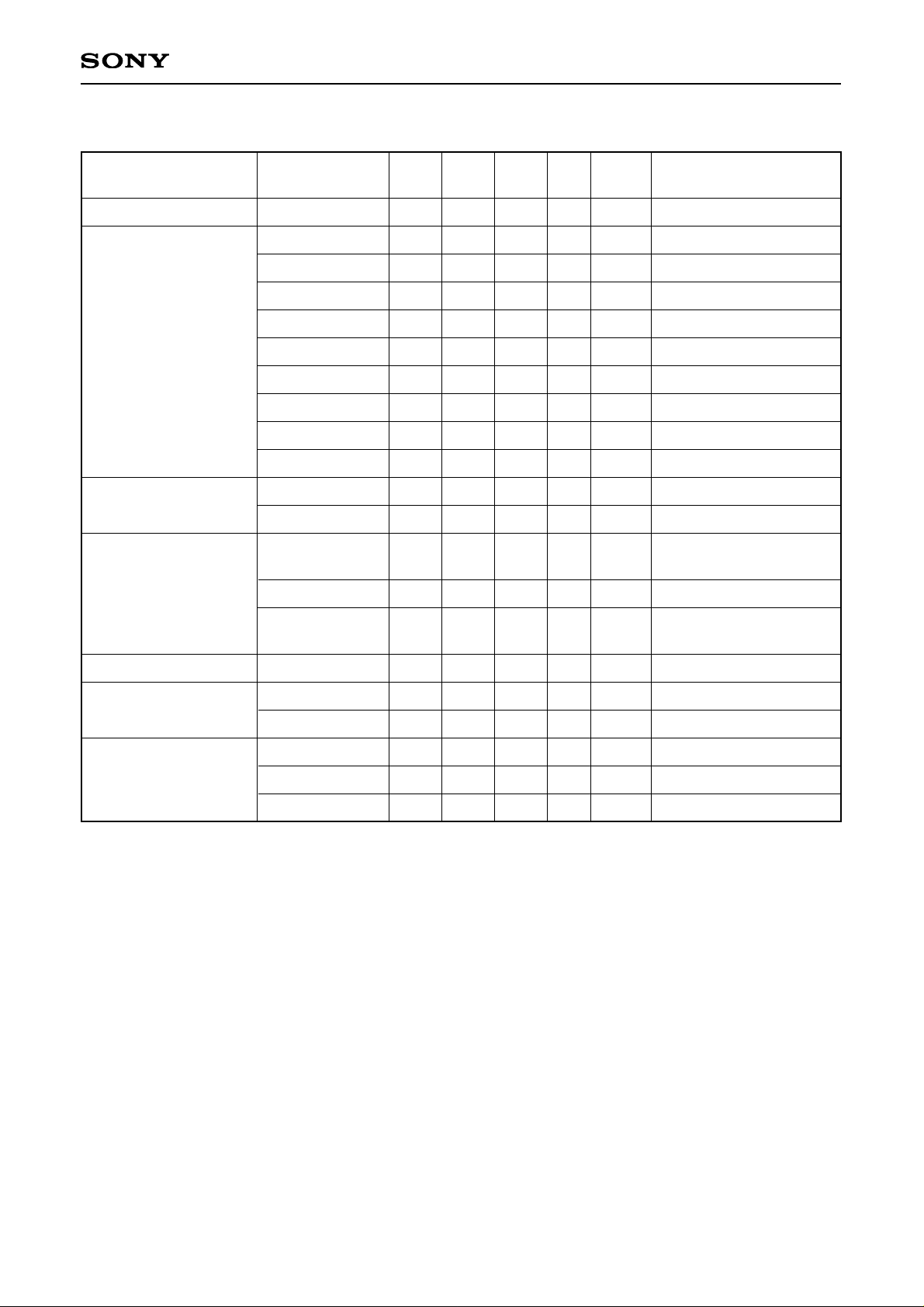
Item
–0.3 to +55
–0.3 to +18
–55 to +10
–15 to +20
to +10
to +15
to +17
–17 to +17
–10 to +15
–55 to +10
–65 to +0.3
–0.3 to +27.5
–0.3 to +22.5
–0.3 to +17.5
–30 to +80
–10 to +60
V
V
V
V
V
V
V
V
V
V
V
V
V
V
°C
°C
∗1
Ratings Unit Remarks
Absolute Maximum Ratings
∗1
+27V (Max.) when clock width < 10µs, clock duty factor < 0.1%.
Substrate voltage SUB – GND
VDD, VOUT1, VOUT2, HIS, CGG1, CGG2 – GND
Supply voltage
VDD, VOUT1, VOUT2, HIS, CGG1, CGG2 – SUB
Vφ1, Vφ2, Vφ3, VHOLDφ, VOGφ – GND
Clock input voltage
Vφ1, Vφ2, Vφ3, VHOLDφ, VOGφ – SUB
Voltage difference between vertical clock input pins
Voltage difference between horizontal clock input pins
Hφ1, Hφ2 – VOGφ
Hφ1, Hφ2 – GND
Hφ1, Hφ2 – SUB
VL – SUB
Vφ2, Vφ3, VDD, VOUT1, VOUT2, HIS, HIGφ1, HIG2, POGφ – VL
RG – GND
Vφ1, CGG1, CGG2, Hφ1, Hφ2, HHGφ1, HHGφ2, VOGφ, VHOLDφ – VL
Storage temperature
Operating temperature
– 4 –
ICX074AL
∗1
Indications of substrate voltage (VSUB) setting value
The setting value of the substrate voltage is indicated on the back of image sensor by a special code.
Adjust the substrate voltage (VSUB) to the indicated voltage.
VSUB code — two characters indication
↑ ↑
Integer portion Decimal portion
The integer portion of the code and the actual value correspond to each other as follows.
Item
VDD
VSUB
VL
14.55
9.0
Indicated
voltage –0.1
15.45
18.5
Indicated
voltage +0.1
15.0
Indicated
voltage
∗2
V
V
V
∗1
Symbol Min. Typ. Max. Unit Remarks
Bias Conditions
DC Characteristics
Value
9 10 11 12 13 14 15 16 17
18
9 A C d E f G h
J
K
<Example> "A5" → VSUB = 10.5V.
∗2
VL setting is the VVL voltage of the vertical transfer clock waveform, or the same power supply as the VL
power supply for the V driver should be used.
∗3
(1)Current to each pin when 18V is applied to VDD, VOUT1, VOUT2, HIS, RG, CGG1, CGG2, GND and SUB
pins, while pins that are not tested are grounded.
(2)Current to each pin when 20V is applied sequentially to Vφ1, Vφ2 and Vφ3 pins, while pins that are not
tested are grounded. However, 20V is applied to SUB pin.
(3)Current to each pin when 15V is applied sequentially to RG, Hφ1 and Hφ2 pins, while pins that are not
tested are grounded. However, 15V is applied to SUB pin.
(4)Current to VL pin when 25V is applied to Vφ2, Vφ3, POGφ, HIGφ1, HIG2, VDD, VOUT1 and VOUT2 pins or
when, 15V is applied to Vφ1, VHOLDφ, VOGφ, CGG1, CGG2, Hφ1, Hφ2, HHGφ1 and HHGφ2 pins, while VL
pin is grounded. However, GND and SUB pins are left open.
(5)Current to GND pin when 20V is applied to the RG pin and the GND pin is grounded.
∗4
Current to SUB pin when 55V is applied to SUB pin, while all pins that are not tested are grounded.
Supply voltage
Substrate voltage
adjustment range
Substrate voltage
adjustment precision
Protective transistor bias
Item
Supply current
Input current
Input current
IDD
IIN1
IIN2
10
1
10
mA
µA
µA
∗3
∗4
Symbol Min. Typ. Max. Unit Remarks
Integer portion of code
– 5 –
ICX074AL
Item
VVT
VVH02
VVH1, VVH2, VVH3
VVL1, VVL2, VVL3
VφV
I VVL1– VVL3 I
VVHH
VVHL
VVLH
VVLL
VφH
VHL
VφRG
V
RGLH –
V
RGLL
VRGH
VφSUB
VVHOLDH, VVOGH
VVHOLDL, VVOGL
VHHG1H, VHHG2H
VHHG1L, VHHG2L
VHHG1M, VHHG2M
14.55
–0.05
–0.2
–8.0
6.8
4.75
–0.05
4.5
VDD
+0.4
21.5
–0.05
–8.0
4.75
–8.0
–0.05
15.0
0
0
–7.5
7.5
5.0
0
5.0
VDD
+0.6
22.5
0
–7.5
5.0
–7.5
0
15.45
0.05
0.05
–7.0
8.05
0.1
0.5
0.5
0.5
0.5
5.75
0.05
5.5
0.8
VDD
+0.8
23.5
0.05
–7.0
5.25
–7.0
0.05
V
V
V
V
V
V
V
V
V
V
V
V
V
V
V
V
V
V
V
V
V
1
2
2
2
2
2
2
2
2
2
3
3
4
4
4
5
6
6
7
7
7
VVH = VVH02
VVL = (VVL01 + VVL03)/2
VφV = VVHn – VVLn (n = 1 to 3)
High-level coupling
High-level coupling
Low-level coupling
Low-level coupling
Input through 0.01µF
capacitance
Low-level coupling
Readout clock voltage
Vertical transfer clock
voltage
Horizontal transfer
clock voltage
Reset gate clock
voltage
Substrate clock voltage
Vertical final stage
accumulation clock voltage
transfer clock voltage
Inter-horizontal register
transfer clock voltage
Symbol Min. Typ. Max. Unit
Waveform
diagram
Remarks
Clock Voltage Conditions
– 6 –
ICX074AL
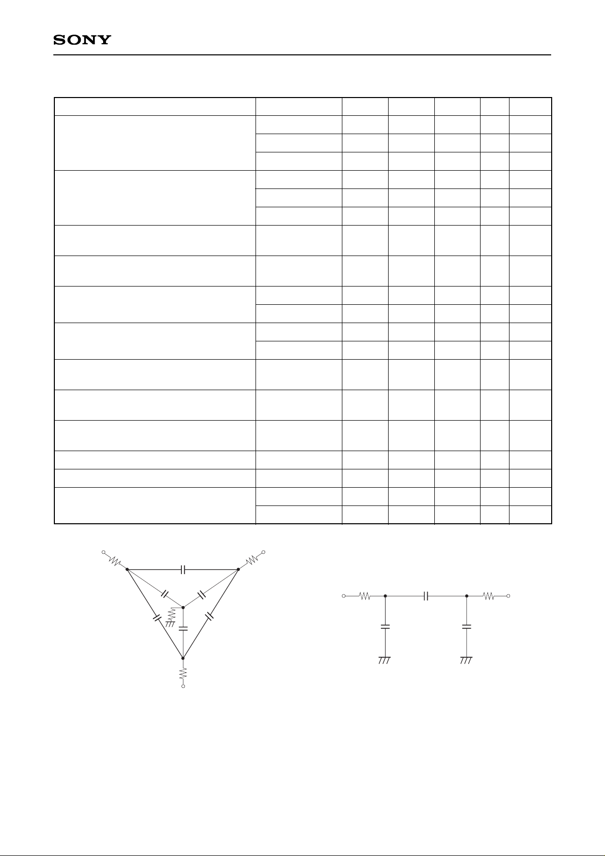
Clock Equivalent Circuit Constant
Item
CφV1
CφV2
CφV3
CφV12
CφV23
CφV31
CφVHOLD
CφVOG
CφHHG1
CφHHG2
CφH1
CφH2
CφHH
CφRG
CφSUB
R1, R2, R3
RGND
RφH1
RφH2
3300
4700
4700
1000
22
100
19
12
23
19
60
69
40
9
400
10
15
24
30
pF
pF
pF
pF
pF
pF
pF
pF
pF
pF
pF
pF
pF
pF
pF
Ω
Ω
Ω
Ω
Capacitance between vertical transfer
clock and GND
Capacitance between vertical transfer
clocks
Capacitance between vertical final stage
accumulation clock and GND
Capacitance between vertical final stage
transfer clock and GND
Capacitance between inter-horizontal
register transfer clock and GND
Capacitance between horizontal transfer
clock and GND
Capacitance between horizontal transfer
clocks
Capacitance between reset gate clock and
GND
Capacitance between substrate clock and
GND
Vertical transfer clock series resistor
Vertical transfer clock ground resistor
Horizontal transfer clock series resistor
Symbol Min. Typ. Max. Unit
Remarks
RφH1
RφH2
Hφ2
CφH1 CφH2
CφHH
Vertical transfer clock equivalent circuit
Horizontal transfer clock equivalent circuit
Hφ1
Vφ1
CφV12
Vφ2
Vφ3
CφV2
RGND
R3
R1
R2
CφV1
Cφv31
Cφv23
CφV3
– 7 –
ICX074AL
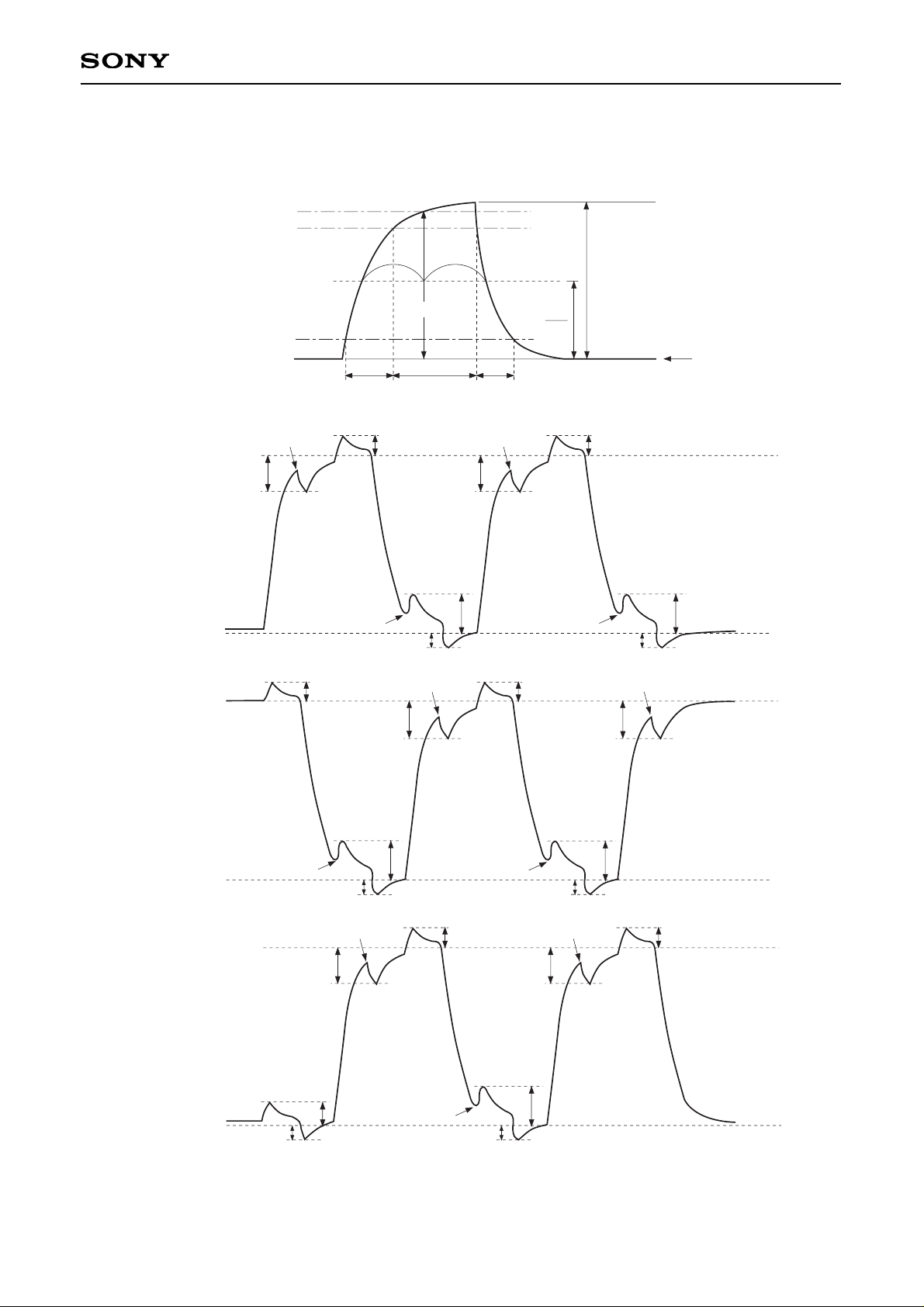
Drive Clock Waveform Conditions
(1) Readout clock waveform
(2) Vertical transfer clock waveform
II II
100%
90%
10%
0%
VVT
tr twh tf
φM
0V
φM
2
Vφ1
VVH1
VVH1
VVHH VVHH VVH
VVHL VVHL
VVLH
VVLH
VVL1
VVL1
VVL01
VVL
VVLL VVLL
Vφ3
VVH3 VVH3
VVHH VVHH VVH
VVHL VVHL
VVLH
VVLH
VVL3
VVL03
VVL
VVLLVVLL
VφV1 = VVH1 – VVL01
VφV2 = VVH02 – VVL2
VφV3 = VVH3 – VVL03
VVH = VVH02
VVL = (VVL01 + VVL03) /2
Vφ2
VVLH
VVL2
VVLL
VVLH
VVL2
VVL
VVLL
VVH
VVHH
VVH02
VVHH
VVH2
VVHL
VVH2
VVHL
 Loading...