

Sony ICX059CL Datasheet
Description
The ICX059CL is an interline CCD solid-state image
sensor suitable for CCIR black-and-white video cameras.
Compared with the current product ICX059AL,
sensitivity is improved drastcally through the adoption
of Super HAD CCD technology.
This chip features a field period readout system and
an electronic shutter with variable charge-storage time.
Features
• High sensitivity (+4dB at F8, +3dB at F1.2 compared with ICX059AL)
• High resolution, low smear and low dark current
• Excellent antiblooming characteristics
• Continuous variable-speed shutter
• Horizontal register: 5V drive
• Reset gate: 5V drive
Device Structure
• Interline CCD image sensor
• Image size: Diagonal 6mm (Type 1/3)
• Number of effective pixels: 752 (H) × 582 (V) approx. 440K pixels
• Number of total pixels: 795 (H) × 596 (V) approx. 470K pixels
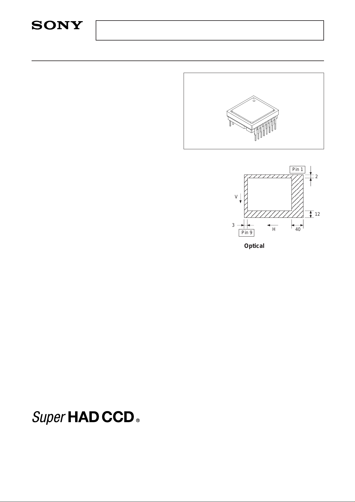
• Chip size: 6.00mm (H) × 4.96mm (V)
• Unit cell size: 6.50µm (H) × 6.25µm (V)
• Optical black: Horizontal (H) direction: Front 3 pixels, rear 40 pixels
Vertical (V) direction: Front 12 pixels, rear 2 pixels
• Number of dummy bits: Horizontal 22
Vertical 1 (even field only)
• Substrate material: Silicon
– 1 –
ICX059CL
E97X22A99
Diagonal 6mm (Type 1/3) CCD Image Sensor for CCIR Black-and-White Video Camera
Sony reserves the right to change products and specifications without prior notice. This information does not convey any license by
any implication or otherwise under any patents or other right. Application circuits shown, if any, are typical examples illustrating the
operation of the devices. Sony cannot assume responsibility for any problems arising out of the use of these circuits.
A
A
A
Pin 1
V
3
40
2
12
Pin 9
H
Optical black position
(Top View)
16 pin DIP (Plastic)
∗
Super HAD CCD is a registered trademark of Sony Corporation. Super HAD CCD is a CCD that drastically improves sensitivity by introducing newly
developed semiconductor technology by Sony Corporation into Sony's high-performance HAD (Hole-Accumulation Diode) sensor.
AAA
AAA
AAA
– 2 –
ICX059CL
Substrate voltage SUB – GND
Supply voltage
Vertical clock input voltage
Voltage difference between vertical clock input pins
Voltage difference between horizontal clock input pins
Hφ1, Hφ2 – Vφ4
Hφ1, Hφ2, LHφ1, RG, VGG – GND
Hφ1, Hφ2, LHφ1, RG, VGG – SUB
VL – SUB
Vφ1, Vφ2, Vφ3, Vφ4, VDD, VOUT – VL
RG – VL
VGG, VSS, Hφ1, Hφ2, LHφ1 – VL
Storage temperature
Operating temperature
Block Diagram and Pin Configuration
(Top View)
1
2
3
4
5
6
7
8
9
10
11
12
13
14 15
16
Note)
Note) : Photo sensor
V
OUT
V
SS
V
GG
GND
Vφ
1
Vφ
2
Vφ
3
Vφ
4
V
DD
GND
SUB
V
L
RG
LHφ
1
Hφ
1
Hφ
2
Horizontal register
Vertical register
Pin No.
1
2
3
4
5
6
7
8
Vφ4
Vφ3
Vφ2
Vφ1
GND
VGG
VSS
VOUT
Vertical register transfer clock
Vertical register transfer clock
Vertical register transfer clock
Vertical register transfer clock
GND
Output amplifier gate bias
Output amplifier source
Signal output
9
10
11
12
13
14
15
16
VDD
GND
SUB
VL
RG
LHφ1
Hφ1
Hφ2
Output amplifier drain supply
GND
Substrate (Overflow drain)
Protective transistor bias
Reset gate clock
Horizontal register final stage transfer clock
Horizontal register transfer clock
Horizontal register transfer clock
Symbol
Description
Pin No.
Description
Pin Description
Absolute Maximum Ratings
–0.3 to +55
–0.3 to +18
–55 to +10
–15 to +20
to +10
to +15
to +17
–17 to +17
–10 to +15
–55 to +10
–65 to +0.3
–0.3 to +30
–0.3 to +24
–0.3 to +20
–30 to +80
–10 to +60
V
V
V
V
V
V
V
V
V
V
V
V
V
V
°C
°C
∗1
VDD, VOUT, VSS – GND
VDD, VOUT, VSS – SUB
Vφ1, Vφ2, Vφ3, Vφ4 – GND
Vφ1, Vφ2, Vφ3, Vφ4 – SUB
Item Ratings Unit Remarks
∗1
+27V (Max.) when clock width < 10µs, clock duty factor < 0.1%.
Symbol
– 3 –
ICX059CL
Bias Conditions
Item
Output amplifier drain voltage
Output amplifier gate voltage
Output amplifier source
Substrate voltage adjustment range
Fluctuation range after substrate voltage adjustment
Reset gate clock voltage adjustment range
Fluctuation range after reset gate clock voltage
adjustment
Protective transistor bias
VDD
VGG
VSS
VSUB
∆VSUB
VRGL
∆VRGL
VL
14.55
3.8
9.0
–3
1.0
–3
15.0
4.2
15.45
4.65
18.5
+3
4.0
+3
V
V
V
%
V
%
±5%
∗1
∗1, ∗6
Symbol Min. Typ. Max. Unit Remarks
DC Characteristics
Item
Output amplifier drain current
Input current
Input current
IDD
IIN1
IIN2
5
1
10
mA
µA
µA
∗3
∗4
Symbol Min. Typ. Max. Unit Remarks
Grounded with
820Ω resistor
∗2
∗1
Indications of substrate voltage (VSUB) · reset gate clock voltage (VRGL) setting value.
The setting values of substrate voltage and reset gate clock voltage are indicated on the back of the image
sensor by a special code. Adjust substrate voltage (VSUB) and reset gate clock voltage (VRGL) to the
indicated voltage. Fluctuation range after adjustment is ±3%.
VSUB code one character indication
VRGL code one character indication ↑ ↑
VRGL code VSUB code
Code and optimal setting correspond to each other as follows.
1
VRGL code
Optimal setting 1.0 1.5 2.0 2.5 3.0 3.5 4.0
2
3
4 5
6
7
VSUB code
Optimal setting
9.0 9.5
10.0 10.5 11.0 11.5 12.012.5 13.0 13.5 14.0 14.5 15.015.5 16.0 16.5 17.0 17.5 18.0 18.5
E f G
h J K L
m
N P
Q
R
S
T
U V W X
Y
Z
<Example> “5L” → VRGL = 3.0V
VSUB = 12.0V
∗2
VL setting is the VVL voltage of the vertical transfer clock waveform.
∗3
1) Current to each pin when 18V is applied to VDD, VOUT, Vss and SUB pins, while pins that are not tested
are grounded.
2) Current to each pin when 20V is applied sequentially to Vφ1, Vφ2, Vφ3 and Vφ4 pins, while pins that are
not tested are grounded. However, 20V is applied to SUB pin.
3) Current to each pin when 15V is applied sequentially to RG, LHφ1, Hφ1, Hφ2 and VGG pins, while pins
that are not tested are grounded. However, 15V is applied to SUB pin.
4) Current to VL pin when 30V is applied to Vφ1, Vφ2, Vφ3, Vφ4, VDD and VOUT pins or when, 24V is applied
to RG pin or when, 20V is applied to VGG, Vss, Hφ1, Hφ2 and LHφ1 pins, while VL pin is grounded.
However, GND and SUB pins are left open.
∗4
Current to SUB pin when 55V is applied to SUB pin, while pins that are not tested are grounded.
– 4 –
ICX059CL
Clock Voltage Conditions
Item
Readout clock voltage
VVT
VVH1, VVH2
VVH3, VVH4
VVL1, VVL2,
VVL3, VVL4
VφV
| VVH1 – VVH2 |
VVH3 – VVH
VVH4 – VVH
VVHH
VVHL
VVLH
VVLL
VφH,VφLH
VHL,VLHL
VφRG
VRGLH – VRGLL
VφSUB
14.55
–0.05
–0.2
–9.0
7.8
–0.25
–0.25
4.75
–0.05
4.5
22.5
15.0
0
0
–8.5
8.5
5.0
0
5.0
23.5
15.45
0.05
0.05
–8.0
9.05
0.1
0.1
0.1
0.5
0.5
0.5
0.5
5.25
0.05
5.5
0.8
24.5
V
V
V
V
V
V
V
V
V
V
V
V
V
V
V
V
V
1
2
2
2
2
2
2
2
2
2
2
2
3
3
4
4
5
VVH = (VVH1 + VVH2)/2
VVL = (VVL3 + VVL4)/2
VφV = VVHn – VVLn (n = 1 to 4)
High-level coupling
High-level coupling
Low-level coupling
Low-level coupling
∗5
∗5
∗6
Low-level coupling
Horizontal transfer
clock voltage
Reset gate clock
voltage
Substrate clock voltage
Vertical transfer clock
voltage
Symbol Min.
Typ. Max.
Unit
Waveform
diagram
Remarks
∗5
The horizontal final stage transfer clock input pin LHφ1 is connected to the horizontal transfer clock input
pin Hφ1.
∗6
The reset gate clock voltage need not be adjusted when reset gate clock is driven when the specifications
are as given below. In this case, the reset gate clock voltage setting indicated on the back of the image
sensor has not significance.
Item
Symbol
VRGL
VφRG
Min.
Typ.
Max.
Unit
Waveform
diagram
–0.2
8.5
0
9.0
0.2
9.5
V
V
4
4
Remarks
Reset gate clock
voltage
– 5 –
ICX059CL
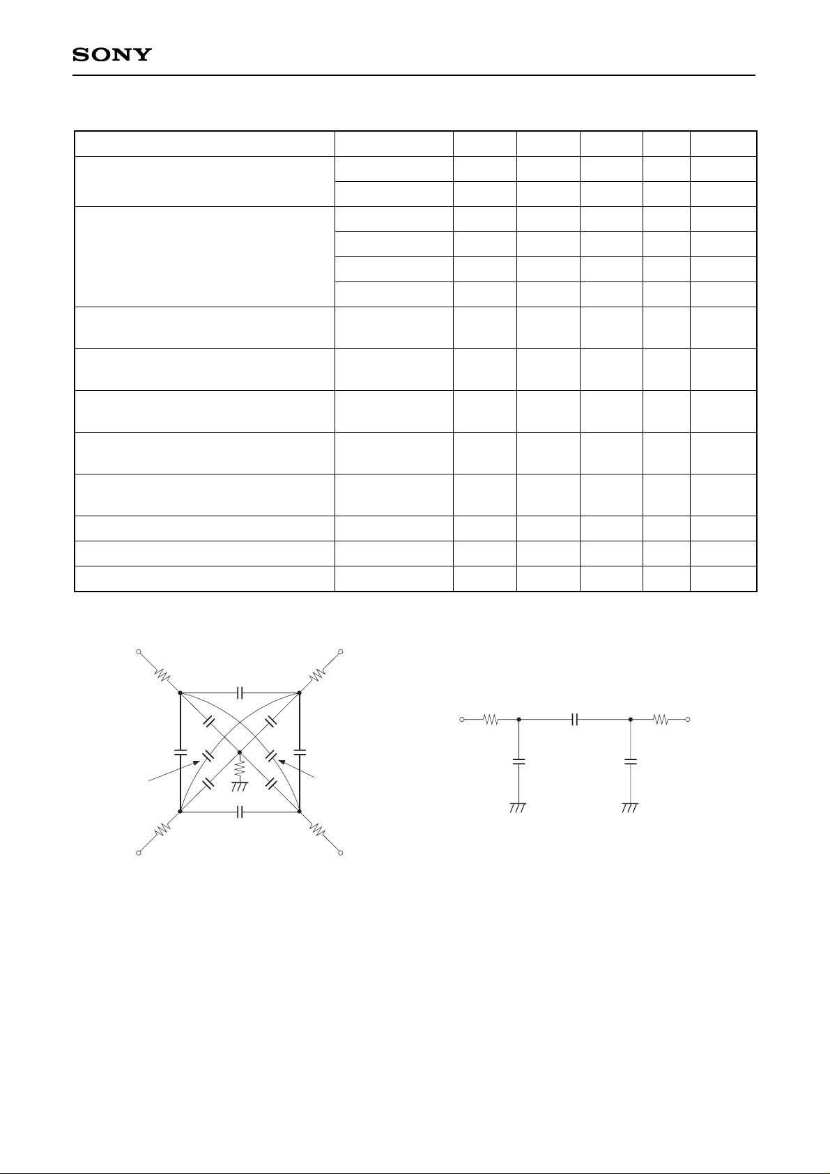
Clock Equivalent Circuit Constant
Item
Capacitance between vertical transfer
clock and GND
CφV1, CφV3
CφV2, CφV4
CφV12, CφV34
CφV23, CφV41
CφV13
CφV24
CφH1, CφH2
CφHH
CφLH
CφRG
CφSUB
R1, R2, R3, R4
RGND
RφH
1000
560
470
390
180
100
47
51
8
8
270
80
15
15
pF
pF
pF
pF
pF
pF
pF
pF
pF
pF
pF
Ω
Ω
Ω
Capacitance between vertical transfer
clocks
Capacitance between horizontal
transfer clock and GND
Capacitance between horizontal
transfer clocks
Capacitance between horizontal final
stage transfer clock and GND
Capacitance between reset gate clock
and GND
Capacitance between substrate clock
and GND
Vertical transfer clock series resistor
Vertical transfer clock ground resistor
Horizontal transfer clock series resistor
Symbol Min. Typ. Max. Unit Remarks
RφH RφH
Hφ2
Hφ1
CφH1
CφH2
CφHH
Vφ1
CφV12
Vφ2
Vφ4 Vφ3
CφV34
CφV23
CφV41
CφV13
CφV24
CφV1 CφV2
CφV4 CφV3
RGND
R4
R1
R3
R2
Vertical transfer clock equivalent circuit Horizontal transfer clock equivalent circuit
– 6 –
ICX059CL
VVH = (VVH1 + VVH2)/2
VVL = (VVL3 + VVL4)/2
VφV = VVHn – VVLn (n = 1 to 4)
Vφ1 Vφ3
Vφ2 Vφ4
VVHH
VVH
VVHL
VVHH
VVHL
VVH1
VVL1
VVLH
VVLL
VVL
VVHH
VVH3
VVHL
VVH
VVHH
VVHL
VVL3
VVL
VVLL
VVLH
VVHH VVHH
VVH
VVHL
VVHL
VVH2
VVLH
VVL2
VVLL
VVL
VVHH VVHH
VVHL
VVH4
VVHL
VVH
VVL
VVLH
VVLL
VVL4
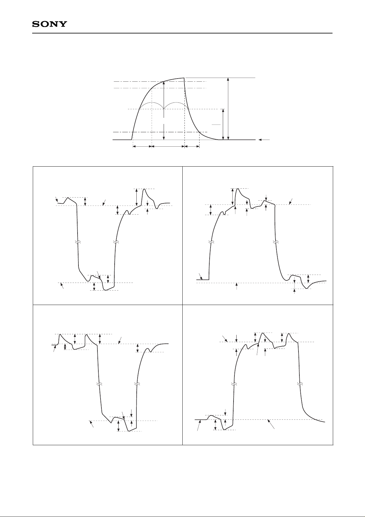
Drive Clock Waveform Conditions
(1) Readout clock waveform
(2) Vertical transfer clock waveform
II II
100%
90%
10%
0%
VVT
tr twh tf
φM
0V
φM
2
 Loading...