

Sony ICX039DNA Datasheet
– 1 –
ICX039DNA
E95Y14C99
Diagonal 8mm (Type 1/2) CCD Image Sensor for PAL Color Video Cameras
Description
The ICX039DNA is an interline CCD solid-state
image sensor suitable for PAL color video cameras
with a diagonal 8mm (Type 1/2) system. Smear,
sensitivity, D-range, S/N and other characteristics
have been greatly improved compared with the
ICX039BNA. High sensitivity and low dark current
are achieved through the adoption of Ye, Cy, Mg and
G complementary color mosaic filters and HAD
(Hole-Accumulation Diode) sensors.
This chip features a field period readout system and
an electronic shutter with variable charge-storage
time.
This chip is compatible with and can replace the
ICX039BNA.
Features
• Low smear (–20dB compared with the ICX039BNA)
• High sensitivity (+3.0dB compared with the ICX039BNA)
• High D range (+2.5dB compared with the ICX039BNA)
• High S/N
• High resolution and low dark current
• Excellent antiblooming characteristics
• Ye, Cy, Mg, and G complementary color mosaic filters on chip
• Continuous variable-speed shutter
• Substrate bias: Adjustment free (external adjustment also possible with 6 to 14V)
• Reset gate pulse: 5Vp-p adjustment free (drive also possible with 0 to 9V)
• Horizontal register: 5V drive
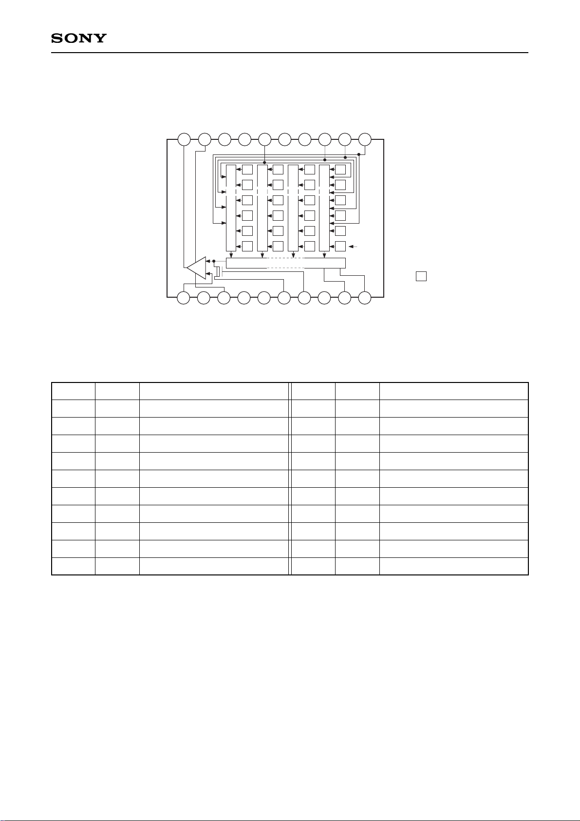
Device Structure
• Interline CCD image sensor
• Image size: Diagonal 8mm (Type 1/2)
• Number of effective pixels: 752 (H) x 582 (V) approx. 440K pixels
• Total number of pixels: 795 (H) x 596 (V) approx. 470K pixels
• Chip size: 7.95mm (H) x 6.45mm (V)
• Unit cell size: 8.6µm (H) x 8.3µm (V)
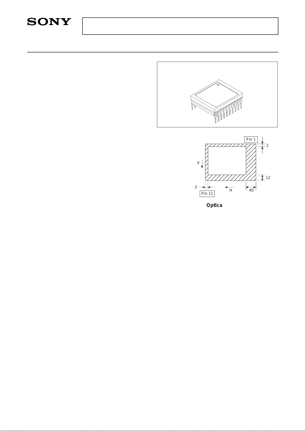
• Optical black: Horizontal (H) direction : Front 3 pixels, rear 40 pixels
Vertical (V) direction : Front 12 pixels, rear 2 pixels
• Number of dummy bits: Horizontal 22
Vertical 1 (even fields only)
• Substrate material: Silicon
Sony reserves the right to change products and specifications without prior notice. This information does not convey any license by
any implication or otherwise under any patents or other right. Application circuits shown, if any, are typical examples illustrating the
operation of the devices. Sony cannot assume responsibility for any problems arising out of the use of these circuits.
20 pin DIP (Cer-DIP)
A
A
A
Pin 1
V
3
40
2
12
Pin 11
H
Optical black position
(Top View)
AAA
AAA
AAA
– 2 –
ICX039DNA
Pin No. Symbol Description Pin No. Symbol Description
1
2
3
4
5
6
7
8
9
10
Vφ4
Vφ3
Vφ2
φSUB
GND
Vφ1
VL
GND
VDD
VOUT
Vertical register transfer clock
Vertical register transfer clock
Vertical register transfer clock
Substrate clock
GND
Vertical register transfer clock
Protective transistor bias
GND
Output circuit supply voltage
Signal output
11
12
13
14
15
16
17
18
19
20
VGG
VDSUB
VSS
GND
GND
RD
φRG
NC
Hφ1
Hφ2
Output circuit gate bias
Substrate bias circuit supply voltage
Output circuit source
GND
GND
Reset drain bias
Reset gate clock
Horizontal register transfer clock
Horizontal register transfer clock
1
2
3
4
5
6
7
8
9
10
11
12
13
14 15
16
Note)
Note) : Photo sensor
GND
V
L
Vφ
1
GND
φ
SUB
Vφ
2
Vφ
3
Vφ
4
V
GG
V
DSUB
V
SS
GND
GND
RD
φ
RG
NC
Horizontal Register
17
18
19
20
V
DD
V
OUT
Hφ
1
Hφ
2
Cy
Mg
Cy
G
Cy
Mg
Ye
G
Ye
Mg
Ye
G
Cy
Mg
Cy
G
Cy
Mg
Ye
G
Ye
Mg
Ye
G
Vertical Register
Block Diagram and Pin Configuration
(Top View)
Pin Description
– 3 –
ICX039DNA
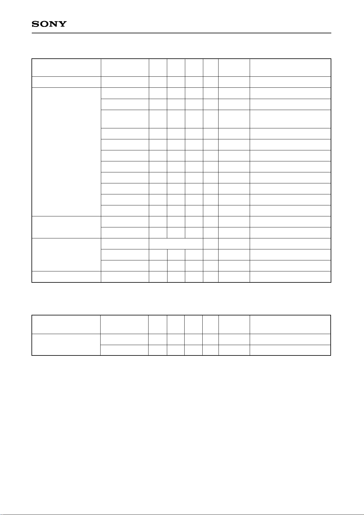
Item
–0.3 to +50
–0.3 to +18
–55 to +10
–15 to +20
to +10
to +15
to +17
–17 to +17
–10 to +15
–55 to +10
–65 to +0.3
–0.3 to +30
–30 to +80
–10 to +60
V
V
V
V
V
V
V
V
V
V
V
V
°C
°C
∗
1
Ratings Unit Remarks
Absolute Maximum Ratings
∗
1 +27V (Max.) when clock width < 10µs, clock duty factor < 0.1%.
Substrate clock φSUB – GND
VDD, VRD, VDSUB, VOUT, VSS – GND
Supply voltage
VDD, VRD, VDSUB, VOUT, VSS – φSUB
Vφ1, Vφ2, Vφ3, Vφ4 – GND
Clock input voltage
Vφ1, Vφ2, Vφ3, Vφ4 – φSUB
Voltage difference between vertical clock input pins
Voltage difference between horizontal clock input pins
Hφ1, Hφ2 – Vφ4
φRG, VGG – GND
φRG, VGG – φSUB
VL – φSUB
Pins other than GND and φSUB – VL
Storage temperature
Operating temperature
– 4 –
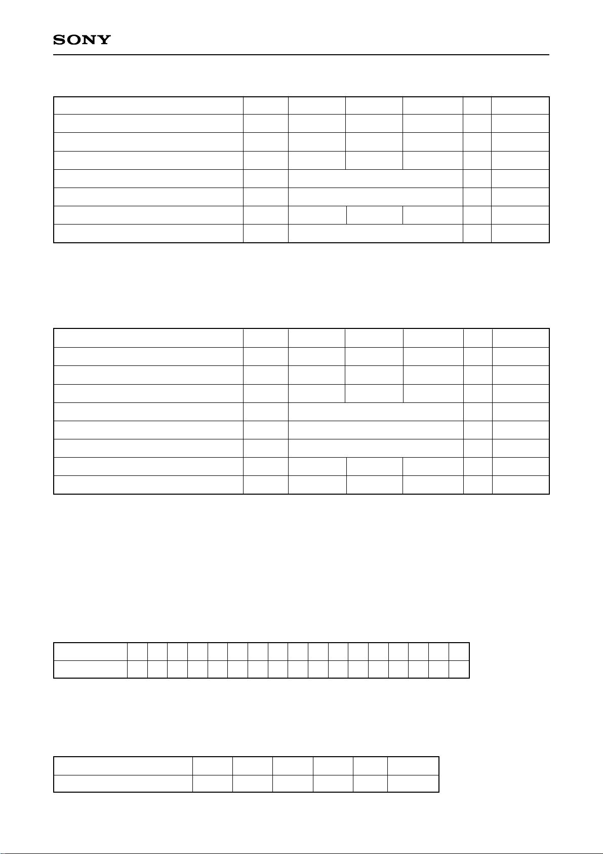
ICX039DNA
Item
VDD
VRD
VGG
VSS
VL
VDSUB
VSUB
∆VSUB
14.55
14.55
1.75
6.0
–3
15.0
15.0
2.0
∗
3
∗
4
15.45
15.45
2.25
14.0
+3
V
V
V
V
%
VRD = VDD
∗
5
∗
5
Symbol Min. Typ. Max. Unit Remarks
Bias Conditions 2 [when used in substrate bias external adjustment mode]
Output circuit supply voltage
Reset drain voltage
Output circuit gate voltage
Output circuit source
Protective transistor bias
Substrate bias circuit supply voltage
Substrate voltage adjustment range
Substrate voltage adjustment precision
∗
3 VL setting is the VVL voltage of the vertical transfer clock waveform, or the same supply voltage as the VL
power supply for the V driver should be used. (When CXD1267AN is used.)
∗
4 Connect to GND or leave open.
∗
5 The setting value of the substrate voltage (VSUB) is indicated on the back of the image sensor by a special
code. When adjusting the substrate voltage externally, adjust the substrate voltage to the indicated
voltage. The adjustment precision is ±3%. However, this setting value has not significance when used in
substrate bias internal generation mode.
VSUB code — one character indication
Code and optimal setting correspond to each other as follows.
DC Characteristics
Item
Output circuit supply current IDD 5.0 10.0 mA
Symbol Min. Typ. Max. Unit Remarks
VSUB code
Optimal setting 6.0 6.5 7.0 7.5 8.0 8.5 9.0 9.5
10.0 10.5 11.0 11.512.0 12.5 13.0 13.5 14.0
E f G h J K L m N P Q R S T U V W
<Example> "L" → VSUB = 9.0V
Item
VDD
VRD
VGG
VSS
VL
VDSUB
φSUB
14.55
14.55
1.75
14.55
15.0
15.0
2.0
∗
1
15.0
∗
2
15.45
15.45
2.25
15.45
V
V
V
V
VRD = VDD
Symbol Min. Typ. Max. Unit Remarks
Bias Conditions 1 [when used in substrate bias internal generation mode]
Output circuit supply voltage
Reset drain voltage
Output circuit gate voltage
Output circuit source
Protective transistor bias
Substrate bias circuit supply voltage
Substrate clock
Grounded with 390Ω resistor
∗
1 VL setting is the VVL voltage of the vertical transfer clock waveform, or the same supply voltage as the VL
power supply for the V driver should be used. (When CXD1267AN is used.)
∗
2 Do not apply a DC bias to the substrate clock pin, because a DC bias is generated within the CCD.
Grounded with 390Ω resistor
– 5 –
ICX039DNA
Item
Readout clock voltage
VVT
VVH1, VVH2
VVH3, VVH4
VVL1, VVL2,
VVL3, VVL4
VφV
| VVH1 – VVH2 |
VVH3 – VVH
VVH4 – VVH
VVHH
VVHL
VVLH
VVLL
VφH
VHL
VRGL
VφRG
VRGLH – VRGLL
VφSUB
14.55
–0.05
–0.2
–9.6
8.3
–0.25
–0.25
4.75
–0.05
4.5
23.0
15.0
0
0
–9.0
9.0
5.0
0
∗
1
5.0
24.0
15.45
0.05
0.05
–8.5
9.65
0.1
0.1
0.1
0.5
0.5
0.5
0.5
5.25
0.05
5.5
0.8
25.0
V
V
V
V
Vp-p
V
V
V
V
V
V
V
Vp-p
V
V
Vp-p
V
Vp-p
1
2
2
2
2
2
2
2
2
2
2
2
3
3
4
4
4
5
VVH = (VVH1 + VVH2)/2
VVL = (VVL3 + VVL4)/2
VφV = VVHn – VVLn (n = 1 to 4)
High-level coupling
High-level coupling
Low-level coupling
Low-level coupling
Low-level coupling
Horizontal transfer
clock voltage
Reset gate clock
voltage∗1
Substrate clock voltage
Vertical transfer clock
voltage
Symbol Min. Typ. Max. Unit
Waveform
diagram
Remarks
Item Symbol Min. Typ. Max. Unit
Waveform
diagram
Remarks
∗
1 Input the reset gate clock without applying a DC bias. In addition, the reset gate clock can also be driven
with the following specifications.
Reset gate clock
voltage
VRGL
VφRG
–0.2
8.509.0
0.2
9.5VVp-p
4
4
Clock Voltage Conditions
– 6 –
ICX039DNA
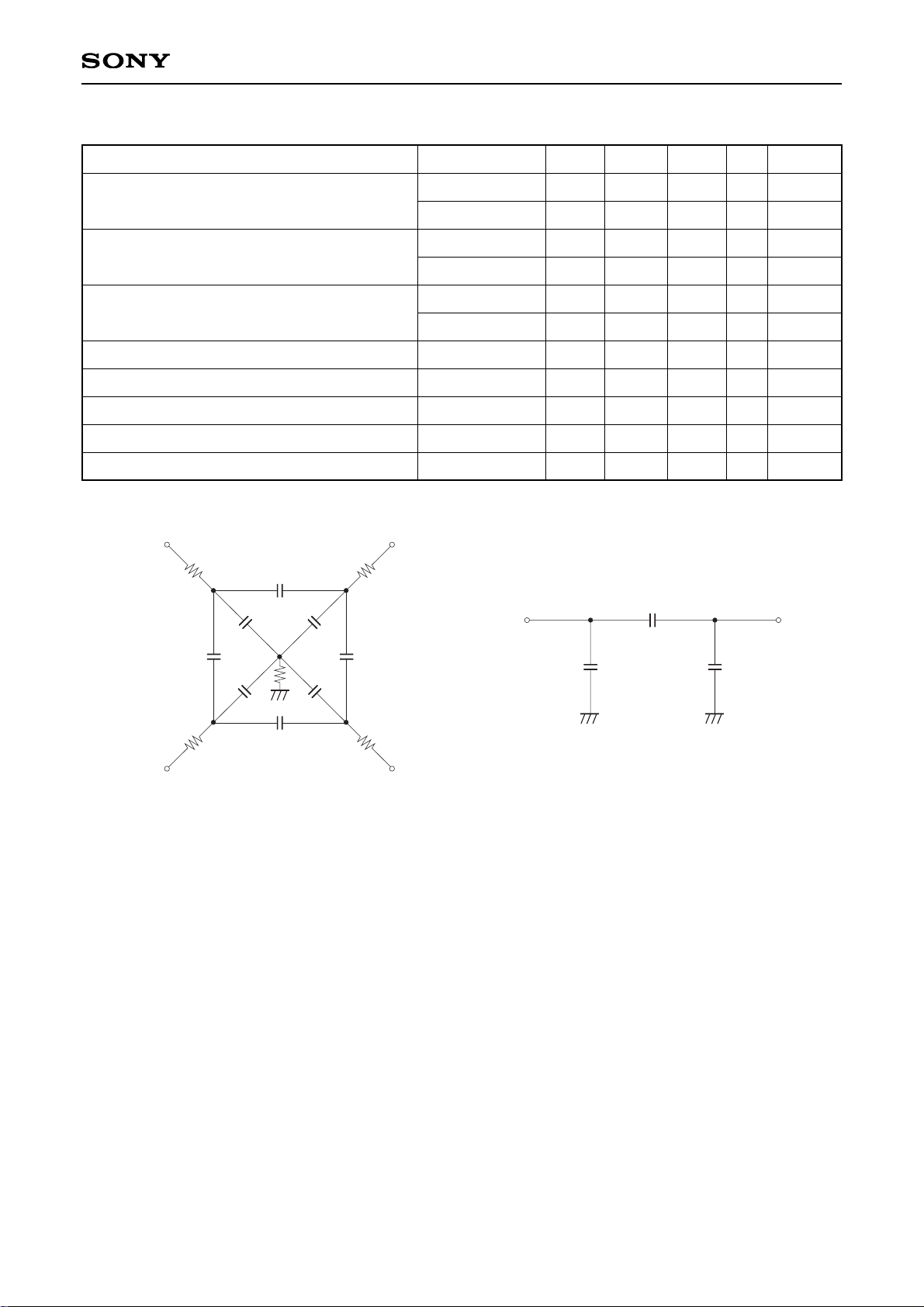
Clock Equivalent Circuit Constant
Item
Capacitance between vertical transfer clock
and GND
CφV1, CφV3
CφV2, CφV4
CφV12, CφV34
CφV23, CφV41
CφH1
CφH2
CφHH
CφRG
CφSUB
R1, R2, R3, R4
RGND
1800
2200
450
270
64
62
47
8
400
68
15
pF
pF
pF
pF
pF
pF
pF
pF
pF
Ω
Ω
Capacitance between vertical transfer clocks
Capacitance between horizontal transfer clock
and GND
Capacitance between horizontal transfer clocks
Capacitance between reset gate clock and GND
Capacitance between substrate clock and GND
Vertical transfer clock series resistor
Vertical transfer clock ground resistor
Symbol Min. Typ. Max. Unit Remarks
Hφ2Hφ1
CφH1 CφH2
CφHH
Vφ1
CφV12
Vφ2
Vφ4 Vφ3
CφV34
CφV23CφV41
CφV1 CφV2
CφV4 CφV3
RGND
R4
R1
R3
R2
Vertical transfer clock equivalent circuit Horizontal transfer clock equivalent circuit
– 7 –
ICX039DNA
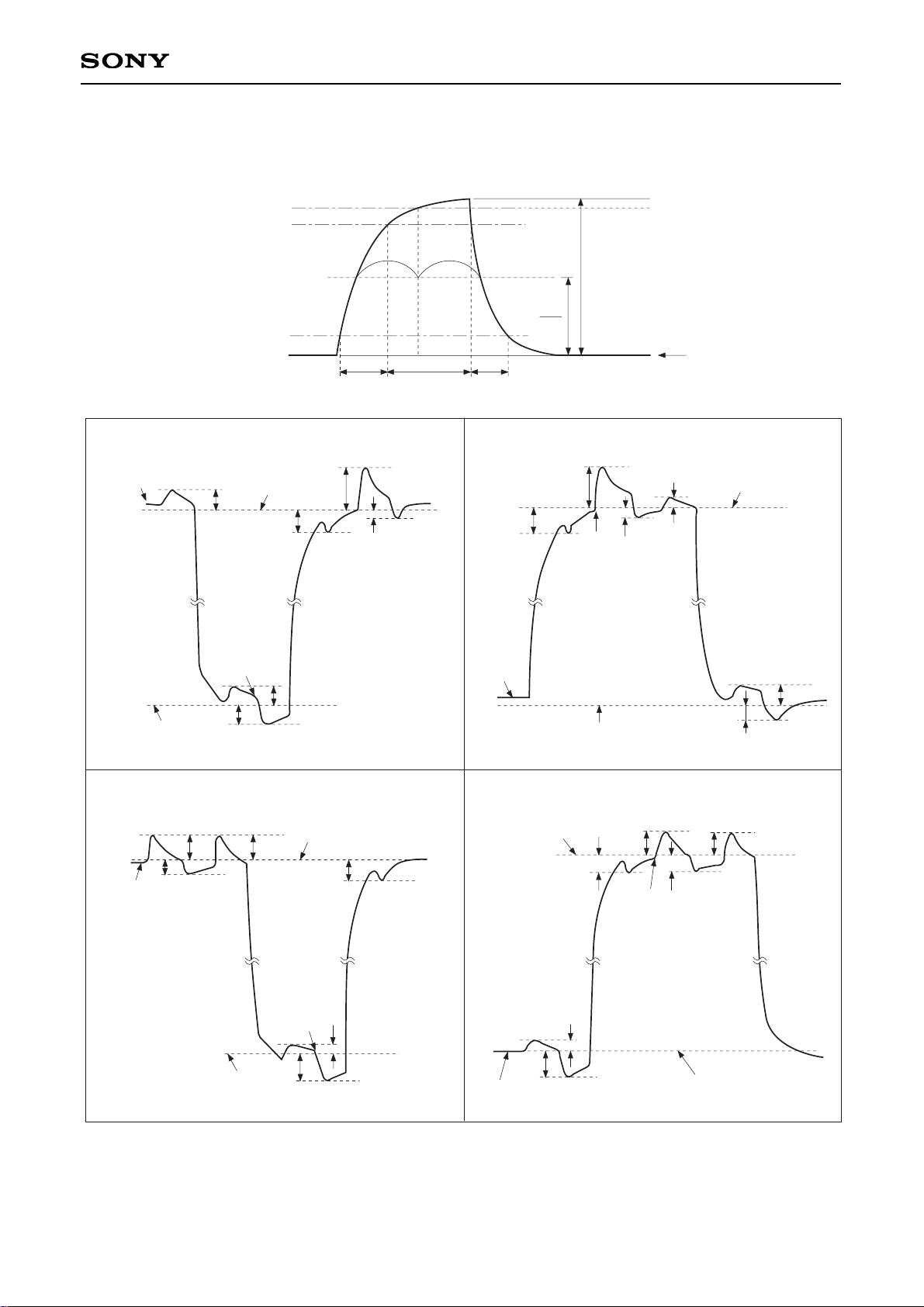
Drive Clock Waveform Conditions
(1) Readout clock waveform
(2) Vertical transfer clock waveform
II II
100%
90%
10%
0%
VVT
tr twh tf
φM
0V
φM
2
Vφ1 Vφ3
Vφ2 Vφ4
VVHH
VVH
VVHL
VVHH
VVHL
VVH1
VVL1
VVLH
VVLL
VVL
VVHH
VVH3
VVHL
VVH
VVHH
VVHL
VVL3
VVL
VVLL
VVLH
VVHH VVHH
VVH
VVHL
VVHL
VVH2
VVLH
VVL2
VVLL
VVL
VVHH VVHH
VVHL
VVH4
VVHL
VVH
VVL
VVLH
VVLL
VVL4
VVH = (VVH1 + VVH2)/2
VVL = (VVL3 + VVL4)/2
VφV = VVHn – VVLn (n = 1 to 4)
 Loading...