

Page 1
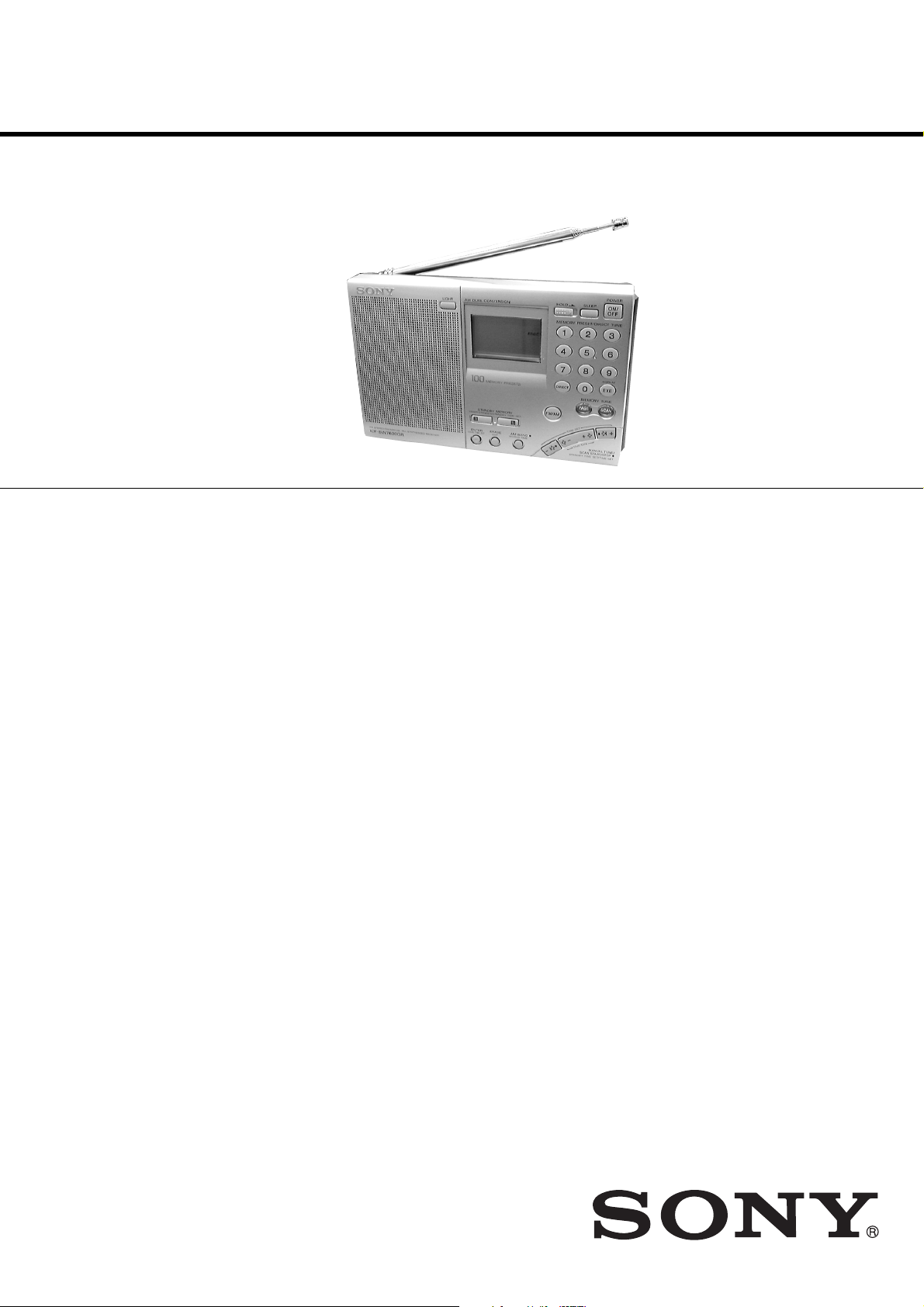
ICF-SW7600GR
SERVICE MANUAL
Ver 1.0 2001. 03
SPECIFICATIONS
Circuit system FM: Super heterodyne
Frequency range FM: 76–108 MHz
Output LINE OUT jack (stereo minijack) × 1
Speaker Approx. 77 mm diameter, 8 Ω × 1
Maximum output 380 mW (at 10 % harmonic distortion)
Power requirements DC 6 V, four R6 (size AA) batteries
External power source DC IN 6V (except Chinese)
Dimensions Approx. 190 × 118.8 × 35.3 mm incl. projecting parts
Mass Approx. 536 g
Supplied accessories
Carrying case (1)
Compact antenna AN-71 (1)
Wave Handbook (1)
AM: Dual conversion super heterodyne
SW: 1 621– 29 999 kHz
MW: 530–1 620 kHz
LW: 150–529 kHz
Recording output level approx. 245 mV, output
impedance less than 10 kΩ
i (headphones) jack (stereo minijack) × 1 16 Ω
(w/h/d)
Approx. 608 g (incl. four R6 (size AA) batteries)
US Model
Canadian Model
AEP Model
Chinese Model
E Model
Tourist Model
9-873-099-11
2001C1600-1
© 2001.3
Design and specifications are subject to change without notice.
FM STEREO/SW/MW/LW
PLL SYNTHESIZED RECEIVER
Sony Corporation
Audio Entertainment Group
General Engineering Dept.
Page 2

ICF-SW7600GR
TABLE OF CONTENTS
1. GENERAL ···································································3
2. DISASSEMBLY
2-1. Cabinet (Rear) ································································· 6
3. ELECTRICAL ADJUSTMENTS ······························6
4. DIAGRAMS
4-1. Block Diagram ······························································· 9
4-2. Printed Wiring Board
– Main Board (Conductor Side) –································ 10
4-3. Printed Wiring Board
– Main Board (Component Side) – ······························ 11
4-4. Schematic Diagram – Main Board (1/2) – ··················· 12
4-5. Schematic Diagram – Main Board (2/2) – ··················· 13
4-6. Printed Wiring Board – KEY Board – ························· 14
4-7. Schematic Diagram – KEY Board – ···························· 15
4-8. IC Pin Function Description ········································ 16
5. EXPLODED VIEWS
5-1. Cabinet Section ···························································· 17
5-2. Chassis Section ···························································· 18
6. ELECTRICAL PARTS LIST ··································· 19
SAFETY-RELATED COMPONENT WARNING!!
COMPONENTS IDENTIFIED BY MARK 0 OR DOTTED LINE WITH
MARK 0 ON THE SCHEMATIC DIAGRAMS AND IN THE PARTS
LIST ARE CRITICAL TO SAFE OPERATION. REPLACE THESE
COMPONENTS WITH SONY PARTS WHOSE PART NUMBERS
APPEAR AS SHOWN IN THIS MANUAL OR IN SUPPLEMENTS
PUBLISHED BY SONY.
2
ATTENTION AU COMPOSANT AYANT RAPPORT
À LA SÉCURITÉ!
LES COMPOSANTS IDENTIFÉS PAR UNE MARQUE 0 SUR LES
DIAGRAMMES SCHÉMATIQUES ET LA LISTE DES PIÈCES SONT
CRITIQUES POUR LA SÉCURITÉ DE FONCTIONNEMENT. NE
REMPLACER CES COMPOSANTS QUE PAR DES PIÈSES SONY
DONT LES NUMÉROS SONT DONNÉS DANS CE MANUEL OU
DANS LES SUPPÉMENTS PUBLIÉS PAR SONY.
Page 3
SECTION 1
GENERAL
ICF-SW7600GR
This section is extracted from
instruction manual.
Front
1 AM EXT ANT (AM
external antenna) jack (35)
2 ATT (attenuator) control
(21)
3 ATT (attenuator) ON/
OFF switch (21)
4 LINE OUT (recording
output) jack (33)
5 2 (headphones) jack (17,
33)
You can enjoy FM stereo
broadcasting by
connecting the optional
stereo headphones to the
unit . When using
headphones, sound from
the speaker will be
muted.
6 DC IN 6V !
(external power input)
jack (10)
7 LIGHT button
When the display is
difficult to see, press this
button to light up the
display for approximately
10 seconds. Pressing the
button again while the
light is on will turn off the
light. Performing button
operations while the light
is on will extend the
lighting time.
8 Display (7)
9 Controls (6)
0 Speaker
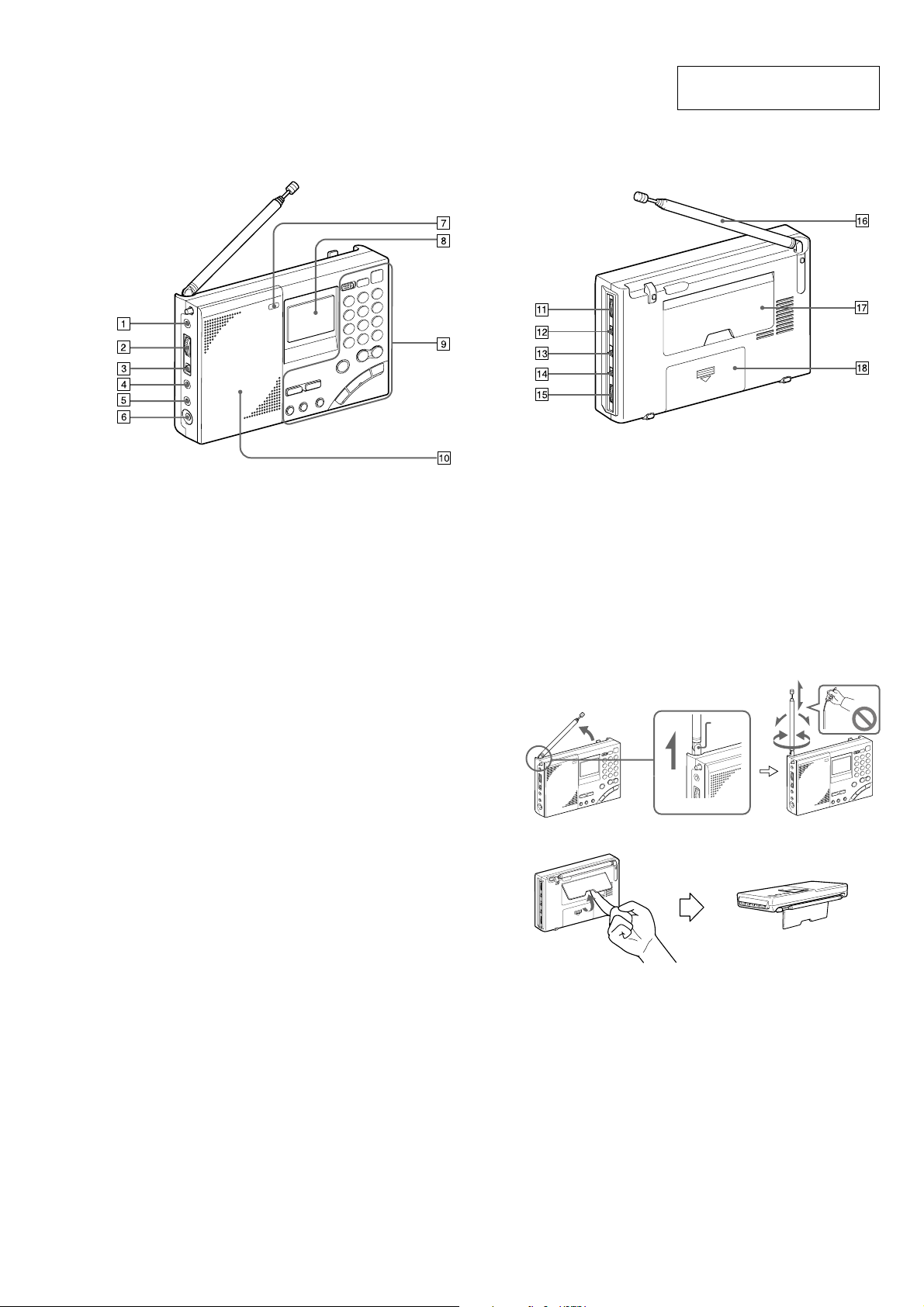
Rear
qa SSB FINE TUNE control (26)
qs LSB/USB selector (26, 27)
qd AM MODE selector (26, 27)
qf TONE selector (33)
qg VOLUME control
qh Telescopic antenna
Always pull out the base of the antenna before use.
Furthermore, do not use unnecessary force when storing the
antenna. At this time, be sure to push in the base as well.
Base
Pull out
qj Stand
qk Battery compartment
3
Page 4
ICF-SW7600GR
Controls
1 SLEEP button (31)
2 HOLD switch (32)
3 DIRECT button (15, 16)
4 FM/AM button (16, 18, 20)
5 STANDBY MEMORY,
TIMER STANDBY/
STANDBY TIME SET
buttons (28, 30)
6 ENTER, LOCAL TIME
SET button (11, 22, 28)
7 ERASE, DST (Daylight
Saving Time) button (11,
13, 30)
8 AM BAND, WORLD
TIME button (13, 18, 20)
9 POWER ON/OFF button
0 Number buttons (15, 16,
22, 23, 24)
qa DISPLAY, EXE button
(13, 15, 16)
Press to switch to clock
display while operating
the radio. Press again to
return to the previous
display. If you do not
press the button, the
display will return to the
previous condition in
about 10 seconds.
qs SCAN button (24)
qd PAGE button (22, 24)
qf MANUAL TUNE/SCAN
START/STOP, STANDBY
TIME SET/TIME SET
buttons (11, 13, 18, 20, 28)
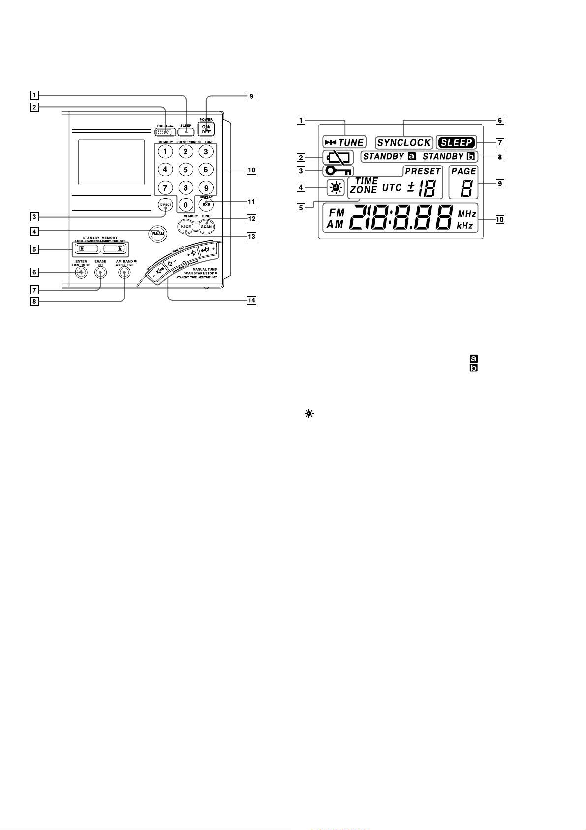
Display
1 TUNE indicator (16, 18)
Appears when a station
is tuned in.
2 Battery indicator (9)
3 HOLD indicator (32)
Appears when HOLD is
in effect. All buttons will
be inoperative.
4
(Daylight Saving
Time) indicator (12)
Appears when the time
display is adjusted to the
Daylight Saving Time.
5 Preset number/time
difference display (11, 22,
23)
6 SYNCLOCK
(synchronous detection
lock) indicator (27)
Appears when
synchronous detection is
in effect.
7 SLEEP indicator (31)
Appears when the sleep
timer is in effect.
8 STANDBY
STANDBY
(28, 29, 30)
Light up when the
standby timer is set.
9 PAGE number display
Appears constantly when
the radio is on.
0 Time/frequency display
,
indicators
4
Page 5
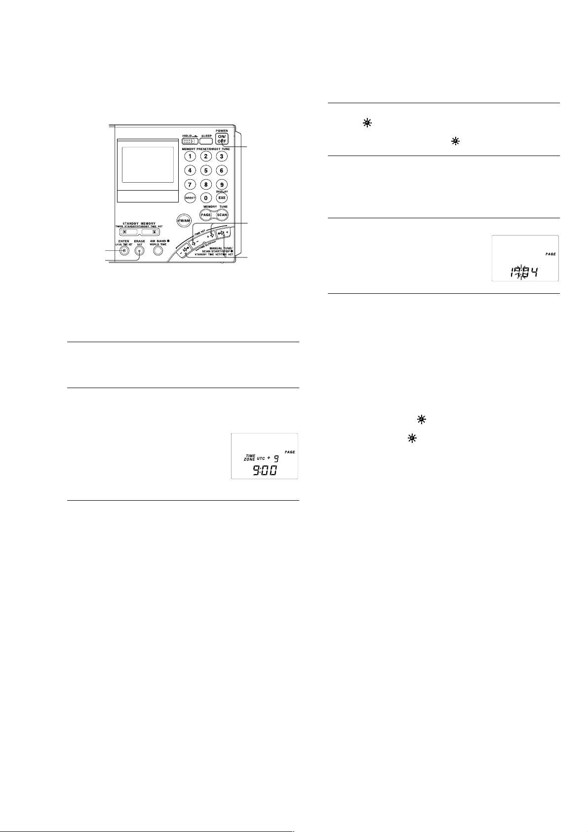
Setting the Current Time
“0:00” flashes in the display when installing the batteries for the first time
or when the unit has been reset. Set the clock to the current time.
1
2
2, 4, 5
3
This unit can display local time, which is the time for your time zone, as
well as world time, which is the time for any other area in the world.
For the calculation of the time in other areas of the world, the time
difference* between the local time and the UTC (Universal Time
Coordinated) is used (see page 14, “Time difference with UTC for each
area”). To find out the correct time, set the correct time and time
difference of the area you are in.
* This unit uses time zones to pinpoint specific areas.
1
If the radio is turned on, press POWER ON/OFF to
turn it off.
Note
You cannot set the clock when the radio is turned on.
2
Hold down LOCAL TIME SET and press K – or + k
to choose the time difference between your local time
and the UTC.
TIME ZONE indicator will appear. Each time you press K – or
+
k, the time difference (UTC + or –) and
the “hour” of the clock will increase or
decrease accordingly.
Two short beeps will be heard when
adjusting the time difference to ±0.
When you release LOCAL TIME SET, the
TIME ZONE indicator will disappear and the time difference with
UTC will be determined.
4
ICF-SW7600GR
3
To set the daylight saving time, press DST to display
the
indicator.
If daylight saving time is not used in your area, daylight saving
time is not currently in effect, or
to Step 4.
4
Hold down LOCAL TIME SET and press –?K or k?
to set the local time.
Each time you press –?K or k?+, the current time will decrease or
increase by a minute. To change the digits rapidly, hold down –?K
or k?+.
Two short beeps will be heard when adjusting the time to “0:00”.
5
Release LOCAL TIME SET.
“ : ” starts flashing and the clock starts
running.
To switch to clock display while the radio is turned on
Press EXE. The display returns to the previous condition
automatically after about 10 seconds or when EXE is pressed
again. The time display period is extended when the WORLD
TIME button is pressed during clock display, or when K – or
+
k is pressed during world time display. During clock display,
radio operations such as changing frequencies are not possible.
The clock will not be displayed during auto scan (page 20) or
memory scan (page 24).
For areas adopting the daylight saving time (summer time)
Press DST to display the
summer time period. When the summer time period has ended,
press DST to clear the
adjusted automatically.
Tips
• The clock is displayed in the 24 hour system.
• Press LOCAL TIME SET to stop the flashing of “0:00”.
• To adjust the time to the second, release LOCAL TIME SET at the time
of the tone.
indicator if you are now in the
indicator. The time display will be
is already displayed, proceed
+
5
Page 6
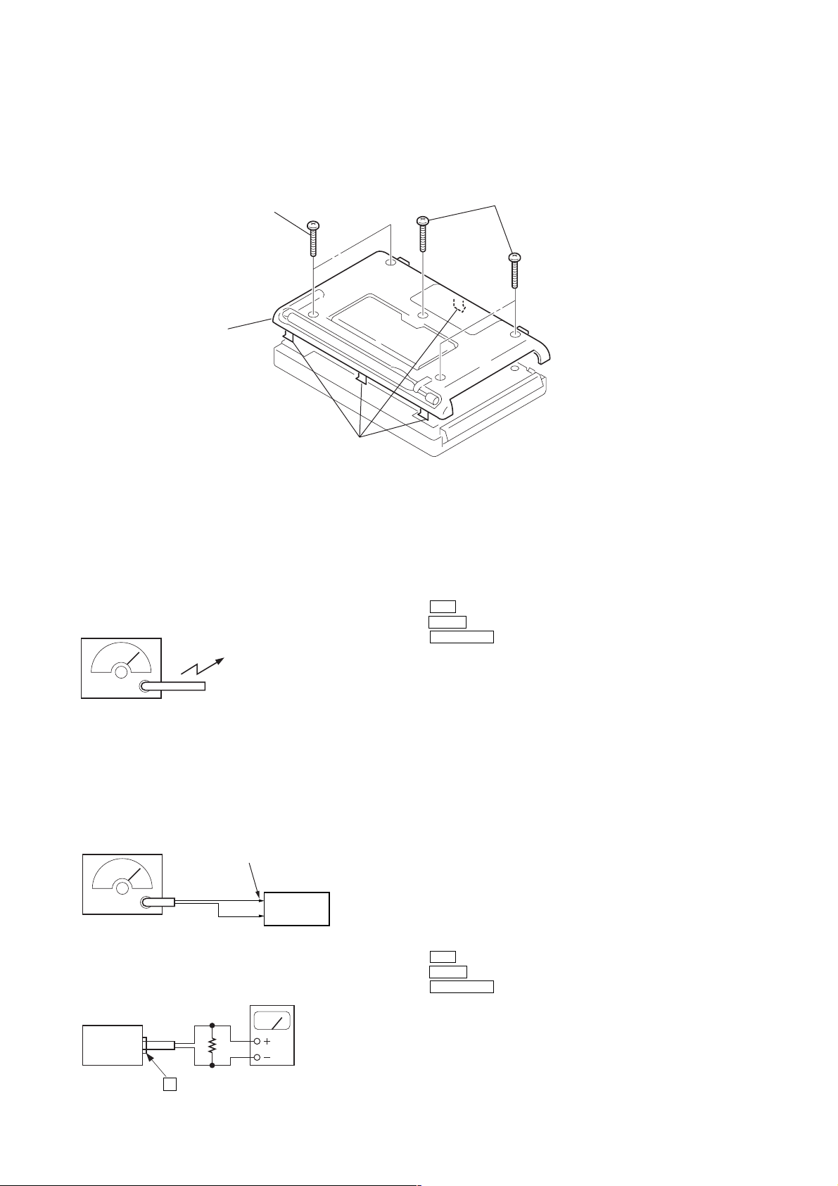
ICF-SW7600GR
r
)
SECTION 2
DISASSEMBLY
Note : Follow the disassembly procedure in the numerical order given.
2-1. CABINET (REAR)
4 Cabinet (rear)
• AM Section
AM RF signal
generator
30% amplitude
modulation by
400Hz signal
output level: as low as possible
• FM Section
FM RF signal
generator
2 Two screws (+BTP 3 × 25)
3 Four claws
ELECTRICAL ADJUSTMENTS
Put the lead-wire
antenna close to
the set.
FM RF IN
1 Three screws (+BTP 3 × 25
SECTION 3
(1) AM / FM VCO Check and Adjustment
Setting:
ATT switch : OFF
TONE switch : MUSIC
AM MODE switch : NORM
Procedure:
1. Connect digital voltmeter to the TP VT.
2. Tune the set to AM 150kHz.
3. Confirm that the reading on the digital voltmeter becomes in
more than 2.2V.
4. Tune the set to AM 29999kHz.
5. Confirm that the reading on the digital voltmeter becomes in
less than 13V.
6. Tune the set to FM 108.00MHz.
7. Confirm that the reading on the digital voltmeter becomes in
less than 13V.
8. IF the value is more than 13V, adjust T202 so that the reading
on the digital voltmeter becomes in 12.5V.
Adjustment Location: MAIN board (See page 8)
22.5kHz frequency
deviation by 400Hz signal
output level: as low as possible
set
6
level mete
16 Ω
i
headphones jack (J202)
set
(2) 1st IF Adjustment
Setting :
ATT switch : OFF
TONE switch : MUSIC
AM MODE switch : NORM
Procedure:
1. Set the frequencies of the AM RF signal generator and the
frequency display of the set to AM 150kHz.
2. Adjust T104 and T105 so that the reading on level meter
becomes in maximum.
Adjustment Location: MAIN board (See page 8)
Page 7
ICF-SW7600GR
r
(3) 2nd Local Adjustment
Setting:
ATT switch : OFF
TONE switch : MUSIC
AM MODE switch : NORM
Procedure:
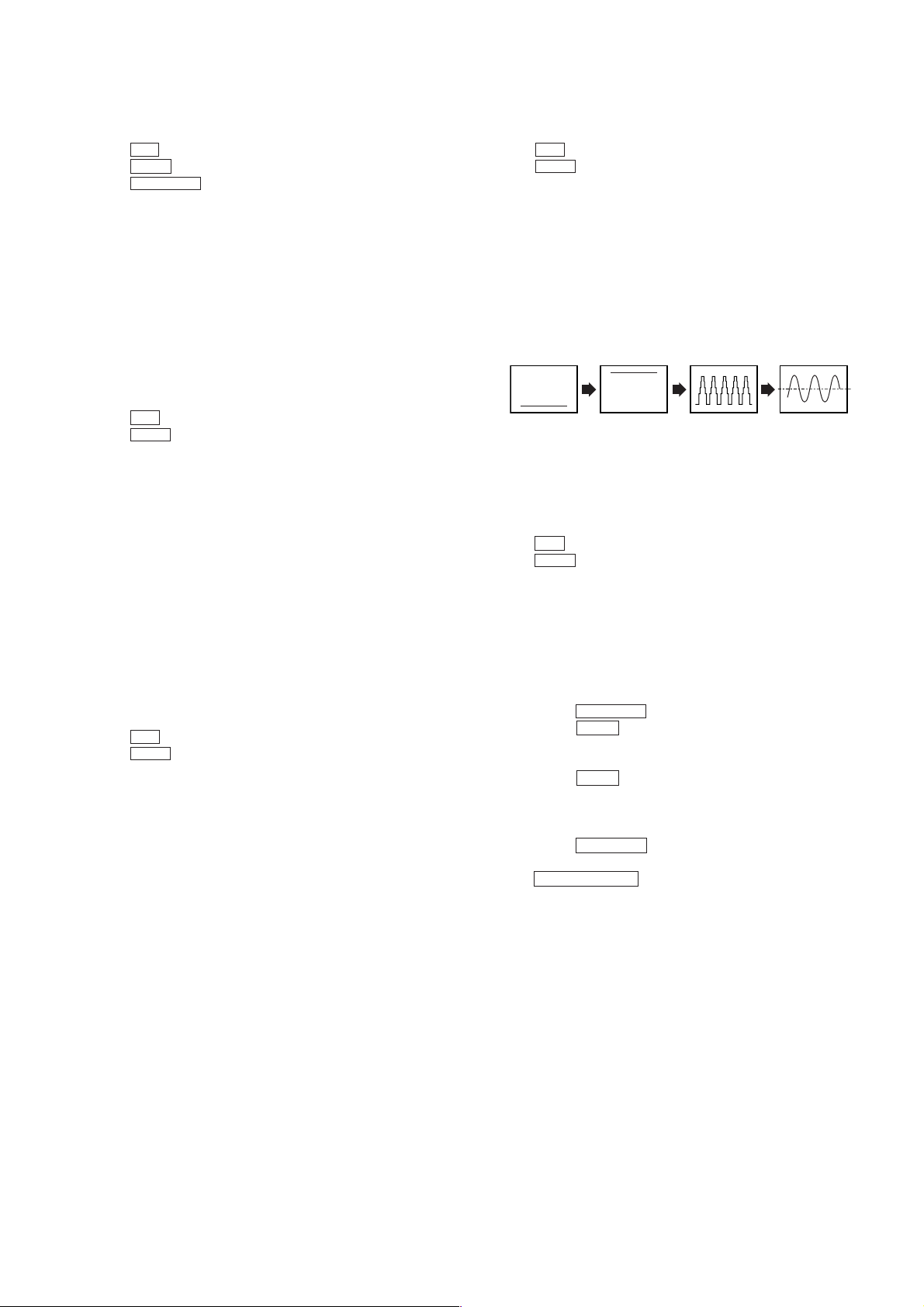
1. Connect frequency counter to the TP OSC2 through the high
input impedance amplifier.
2. Tune the set to AM 150kHz.
3. Adjust CT202 so that the reading on the frequency counter
becomes in 55.39000MHz±30Hz.(55.38997 to 55.39003MHz)
Adjustment Location: MAIN board (See page 8)
(4) FM Tracking Adjustment
Setting:
ATT switch : OFF
TONE switch : MUSIC
Procedure:
1. Set the frequency of the FM RF signal generator and the
frequency display of the set to FM 108.00MHz.
2. Adjust CT101 and CT102 so that the reading on level meter
becomes in maximum.
3. Set the frequency of the FM RF and the frequency display of
the set to FM 76.00MHz.
4. Adjust T101 and T102 so that the reading on level meter
becomes in maximum.
5. Repeat the above steps 1 to 4 several times.
Adjustment Location: MAIN board (See page 8)
(5) 76kHz (MPX) Adjustment
Setting:
ATT switch : OFF
TONE switch : MUSIC
Procedure:
1. Insert Headphones plug into headphones jack (J202) (for VCO
operation).
2. Connect a capacitor (10µF) between IC202 pin1 and GND.
3. Connect frequency counter to the TP 76K (VCO) through the
high input impedance amplifier.
4. Tune the set to FM 108.00MHz.
5. Adjust RV203 so that the reading on the frequency counter
becomes in 76kHz±300Hz.
6. Remove the headphones plug.
(6) Just Tune Adjustment
Setting :
ATT switch : OFF
TONE switch : MUSIC
(FM RF signal generator)
Frequency : 93.025MHz
Moduration : 22.5kHz
Output level : 54dB
Procedure:
1. Connect an oscilloscope to the TP SD.
2. Tune the set to FM 93.00MHz.
3. Adjust R V202 so that the wa veform on the oscilloscope satisfy
as shown the figure.
Cente
NG
Adjustment Location: MAIN board (See page 8)
(7) SSB 0 Beat Adjustment
Setting :
ATT switch : OFF
TONE switch : MUSIC
(AM RF signal generator)
Frequency : AM 150kHz
Moduration : None
Output level : 44dB
Procedure:
1. Connect an oscilloscope to the TP DET.
2. Tune the set to AM 150kHz.
3. Set the AM MODE switch to SYNC.
4. Set the SYNC switch to USB.
5. Adjust CT201 so that the waveform on the oscilloscope is
minimized.
6. Set the SYNC switch to LSB.
7. Adjust CT201 so that the waveform on the oscilloscope is
minimized.
8. Repeat the above steps 4 to 7 several times.
9. Set the AM MODE switch to SSB.
10. Confirm that the beat sound is changed by turning the
SSB FINE TUNE control.
Adjustment Location: MAIN board (See page 8)
NG
NG
OK
Adjustment Location: MAIN board (See page 8)
7
Page 8
ICF-SW7600GR
E
1
C
Adjustment Location :
[MAIN BOARD] — Component Side —
1st IF
Adjustment
T104 T105
T101 T102
FM TRACKING
Adjustment
(76MHz)
FM TRACKING
Adjustment
(108MHz)
CT101 CT102
CT202
2nd LOCAL
Adjustment
T202
FM
VCO
Adjustment
RV202
JUST TUN
Adjustment
RV203
76kHz
(MPX)
Adjustment
IC201
CT201
SSB
0 BEAT
Adjustment
[MAIN BOARD] — Conductor Side —
2C 2E
RV202
RV203
C231
5
1
B
C
E
RV204
VOLUME
C272
1
45
B
E
B
C
E
1E
1C
2B
1B
2C
2E
2C
2B
E
1C
1B
8
KA
K
2B
2C
E
1C
1B
CT201
C267
CF201
CF203
C209
C
18
C253
Adjustment
E
15
CF204
CF205
1
IC203
DET
SSB
0 BEAT
IC201
76K (VCO)
Adjustment
MPX
T202
C
B
C260
C259
Adjustment
CT102
E
A
JUST
TUNE
SD
T102
G
S
T101
C135
A
CT101
D
K
B
A
C
E
E
C
B
CT202
K
C262
C261
K
AAK
E
C
B
OSC2
2nd
LOCAL
AM/FM VCO
Adjustment
Adjustment
16
X201
30
C221
916
VT
S
T103
A
G
D
B
C
G
S
E
K
C152
CN201
2
18
D
T107
C
1
17
8
Page 9

4-1. BLOCK DIAGRAM
ICF-SW7600GR
SECTION 4
DIAGRAMS
J101
AM EXT ANT
(EXCEPT CH)
S101
ATT
OFF
ON
RV101
ATT
ANT101
(TELESCOPIC)
ROD B
BAR B
TO Q112-116
REG
Q120
ATT
Q106
ATT
ANT102
(FERRITE-ROD)
FM TRACKING FM TRACKING
T101
CT101
FM ANT
Q112,113
ATT
BPF
Q105
ATT
Q101
MUTING
CONTROL
Q114,115
AGC
AGC
VT
MUTING
Q107
SW
RF AMP
Q116
LW/MW
RF AMP
Q104
FM
RF AMP
+
Q108,121
AGC
AGC
T102
FM RF
VT
CT102
Q109,110
AM MIX
Q119
1ST OSC
AMP
Q118
1ST OSC
VT
T104
AM MIX2
1ST IF
XF101
55.845MHz
Q117
AM VCO
AMP
T105
AM IFT1
VCOL
Q111
1ST
IF AMP
AM REG
Q206
FM VCO
BUFFER
VCOH
Q205
BAND
SWITCH
20
19
15
T202
FM VCO
FEOUT FMIFOUT
FMRF
AMIN
BAND
FMOSC
22 23
CF202
10.7MHz
16 13
CF201
455kHz
AMOSC-I
X201
AM OSC2
55.390MHz
VT
Q207
AM/FM
SWITCH
AM REG
IC201
FM/AM FRONT-END
IF,DET
FMIFIN
14 5
AMIFIN
AMOSC-O
CF204
3.64MHz
CT202
CERALOCK
Q203
MUTING
24 7 6 8 27
REG
2ND LOCAL
CF203
10.7MHz
11 9
CF205
DISCRI
10.7MHz
SYNC/SSB
CT201
SSB
0 BEAT
MUTING
Q202
SWITCH
RV201
SSB
FINE TUNE
SWITCH
AM REG
FMLIMIN
DISCRI
VCO
(EXCEPT
EA)
Q202
AM MODE
– SSB SYNC NORM –
DET
METER
SD-OUT
SD-CTRL/AGC
U/L
Q201
SWITCH
S201
30
2
26
1
29
ENV/PSN
Q201
SWITCH
METER
AGC
Q208
SWITCH
SD
RV202
JUST
TUNE
S202
SYNC
LSB
USB
Q101
MUTING
CONTROL
Q209
FM
HIGH CUT
Q210
SWITCH
FM REG
MUTING
Q210
AM
HIGH CUT
AM REG
MUTING
Q211
MUTING
S301 - 323
S325 - 328
BATT
HOLD
FREE
KEY
MATRIX
VDD
8
2
2
2
S329
HOLD .
IC301
EEPROM
SDA
SCK
IC305
3.0V REG
IC303
3.5V DET
IC304
3.1V DET
X301
75kHz
LCD1
LIQUID CRYSTAL DISPLAY
Q301
LED DRIVE
Q303,306
PLL LPF
Q304
FM VCO
AMP
D301(BACK LIGHT)
Q302
CURRENT REG
B+ SWITCH
Q305
AM/FM
IC202
PLL FM MPX
J201
LINE OUT
SP201
(SPEAKER)
(HEADPHONES)
• Abbreviation
CH: Chinese model
EA: Saudi Arabia model
EXCEPT CH
J203
DC IN 6V
J202
IC203
Q222,225
B+ SWITCH
SWITCH
Q214
LINE AMP
Q213
LINE AMP
OUT2
OUT1
VCC
Q223
7
10
9
• Signal Path
: FM
Q224
B+ SWITCH
BATT
DRY BATTERY
SIZE"AA"
(IEC DESIGNATION R6)
4PCS,6V
: MW/LW
: SW
IN
VCO
DC/DC
CONVERTER
AM/FM
B+ SWITCH
AM/FM
B+ SWITCH
STOP
Q216
Q220
Q221
L
R
10
8
CONTROL
REG
Q212
STEREO
NEWS
MUSIC
BEEP
RV204
VOLUMEw
MUTING
IC204
+3V REG
S203
TONE
72
Q215
MUTING
PRE/POWER AMP
IN2 L
1
16
IN1 R
NF2
4
NF1
13
14
VOL
1 9
4
RV203
76k(MPX)
MUTING
BEEP
SD
METER
VT
+13V
VCOL
VCOH
REG
AM B
ROD B
BAR B
Q217
AM/FM
B+ SWITCH
Q218
AM/FM
B+ SWITCH
Q219
AM/FM
B+ SWITCH
FM REG
AM REG
+13V
XIN
XOUT
KS0-6
KR0-3
HOLD
SI/SO
SCK
VDD
VDET
CE
IC302
LCD0-14
COM0-3
LIGHT
MUTING
BEEP
METER
VCOL
VCOH
AM/FM
BAR/ROD
POWER
35
ı
49
31
ı
34
1
2
52
53
SD
54
19
EO
20
21
16
17
15
DIGITAL TUNING SYSTEM CONTROL
25
24
9
ı
3
13
ı
10
14
5
6
56
55
233
511
501
99
Page 10

ICF-SW7600GR
4-2. PRINTED WIRING BOARD – MAIN BOARD (CONDUCTOR SIDE) –
A
B
C
D
E
F
G
H
I
MAIN BOARD
EXCEPT EA
RV201
SSB FINE
TUNE
S202
SYNC
USB
LSB
E
C
B
S201
AM MODE
SSB
SYNC
NORM
10
B
S203
TONE
MUSIC
NEWS
B
E
12
E
C
IC202
VOLUMEw
RV203
76K(VCO)
C231
C
RV204
(CONDUCTOR SIDE)
2E
2C
1B
2B
1C
1E
1E
1C
2B
1B
2C
2E
RV202
C272
B
E
C
1E
1C
2B
1B
2C
2E
2C
2B
1C
1B
8
TP
B
E
56
1
TP
DET
1
IC204
45
KA
2B
2C
E
1C
1B
AK
T203
34567891011121314
CT201
E
C267
B
E
CF204
15
CF205
1
CF201
CF203
C209
C
18
IC203
C253
T203
CF202
C
IC201
ANT101
FM/SW
TELESCOPIC
ANT102
MW/LW
FERRITE-ROD
ANTENNA
C128
2E
2B
1C
C121
G
2C
1B
1E
2C
1B
1E
T106
XF101
T105
G
S
D
A
C
C260
T202
B
C259
CT102
E
A
TP
OSC2
K
K
T102
K
B
A
E
CT202
C262
C
C261
G
D
S
CT101
C
E
E
B
C
B
16
X201
TP
SD
30
C221
916
T104
T101
A
K
A
C135
K
S
G
D
S
D
B
E
K
TP
VT
A
C
C152
S
T107
CN201
2
18
G
17
T103
1
A
G
D
C150
B
K
K
A
B
E
2E
2B
1C
EB
C
C
E
A
A
K
K
C157
S
D
C
E
C
C
E
B
B
2C
2E
1B
2B
1E
1C
ANTENNA
UNPLUGGED
PLUGGED
CH
ORG
GRN
BLK
PNK
G
S
C146
C
E
C
B
A
(SPEAKER)
E
C
B
2B
2C
1C
B
E
B
E
E
1B
C
D
C
E
B
E
C
B
C
E
B
B
E
K
C
E
B
E
C
B
C
A
K
B
B
C
E
E
C245
C274
CH
RV101
ATT
K
A
S101
ATT
ON
OFF
C
J101
AM EXT ANT
J201
LINE OUT
J202
A
TO
KEY BOARD
SP201
SPEAKER
8Ω
DRY BATTERY
SIZE "AA"
(IEC DESIGNATION R6)
4PCS. 6V
A
K
K
A
K
CH
A
J203
DC IN 6V
11
1-679-368-
(11)
• Semiconductor Location
Ref. No. Location
D101 D-8
D102 D-7
D103 E-12
D104 E-14
D105 D-10
D106 C-10
D107 D-10
D108 D-10
D109 E-9
Ref. No. Location
D110 E-13
D111 E-8
D201 D-7
D202 I-3
D203 H-3
D204 H-14
D205 H-13
D206 F-6
D207 I-14
Ref. No. Location Ref. No. Location Ref. No. Location Ref. No. Location
IC201 D-5
IC202 F-2
IC203 F-5
IC204 G-3
Q101 E-8
Q104 D-7
Q105 D-12
Q106 D-13
Q107 E-11
Q108 C-10
Q109 C-9
Q110 D-9
Q111 C-7
Q112 D-13
Q113 D-13
Q114 D-12
Q115 D-12
Q116 C-13
Q117 E-10
Q118 D-10
Q119 D-9
Q120 D-12
Q121 C-11
Q201 C-3
Q202 C-3
Q203 E-4
Q204 D-2
Q205 C-5
Q206 E-7
Q207 E-7
Q208 E-6
Q209 E-3
Q210 F-3
Q211 F-3
Q212 F-2
Ref. No. Location Ref. No. Location
Q213 F-13
Q214 F-13
Q215 H-2
Q216 H-3
Q222 F-12
Q223 F-11
Q224 F-12
Q225 F-12
Q217 F-10
Q218 F-10
Q219 F-11
Q220 F-11
Q221 F-11
1010
Note on Printed Wiring Boards:
• X : parts extracted from the component side.
a
•
: Through hole.
• : Pattern from the side which enables seeing.
(The other layers' patterns are not indicated.)
Caution:
Pattern face side: Parts on the pattern face side seen from
(Conductor Side) the pattern face are indicated.
Parts face side: Parts on the parts face side seen from
(Component Side) the parts face are indicated.
• Abbreviation
CH : Chinese model.
EA : Saudi Arabia model.
Page 11

4-3. PRINTED WIRING BOARD – MAIN BOARD (COMPONENT SIDE) –
A
MAIN BOARD
(COMPONENT SIDE)
B
C
D
ICF-SW7600GR
E
F
G
H
US
B
TO
KEY BOARD
I
1-679-368-
11
(11)
15 16
17 18 19 20 21 22 23 24 25 26 27 28
Note on Printed Wiring Boards:
• X : parts extracted from the component side.
a
•
• : Pattern from the side which enables seeing.
(The other layers' patterns are not indicated.)
Caution:
Pattern face side: Parts on the pattern face side seen from
(Conductor Side) the pattern face are indicated.
Parts face side: Parts on the par ts face side seen from
(Component Side) the parts face are indicated.
: Through hole.
1111
Page 12

ICF-SW7600GR
4-4. SCHEMATIC DIAGRAM – MAIN BOARD (1/2) –
Note on Schematic Diagram:
• All capacitors are in µF unless otherwise noted. pF: µµF
50 WV or less are not indicated except for electrolytics
and tantalums.
• All resistors are in Ω and 1/
specified.
• C : panel designation.
• A : B+ Line.
• H : adjustment for repair.
• Voltages and waveforms are dc with respect to ground
under no-signal (detuned) conditions.
4
W or less unless otherwise
• Voltages are taken with a VOM (Input impedance 10 MΩ).
Voltage variations may be noted due to normal production tolerances.
• Voltage variations may be noted due to normal production tolerances.
• Signal path.
F : FM
L : MW/LW
h : SW
• Abbreviation
CH : Chinese model
1212
Page 13

ICF-SW7600GR
4-5. SCHEMATIC DIAGRAM – MAIN BOARD (2/2) –
IC B/D
• Refer to page 16 for IC Block Diagrams.
1
IC B/D
Note on Schematic Diagram:
• All capacitors are in µF unless otherwise noted. pF: µµF
50 WV or less are not indicated except for electrolytics
and tantalums.
• All resistors are in Ω and 1/
specified.
¢
•
• C : panel designation.
• A : B+ Line.
• H : adjustment for repair.
• Voltages and waveforms are dc with respect to ground
• Voltages are taken with a VOM (Input impedance 10 MΩ).
• Voltage variations may be noted due to normal produc-
• Signal path.
• Abbreviation
: internal component.
under no-signal (detuned) conditions.
Voltage variations may be noted due to normal production tolerances.
tion tolerances.
F : FM
L : MW/LW
h : SW
CH : Chinese model
EA : Saudi Arabia model
4
W or less unless otherwise
2
IC B/D
IC B/D
• WAVEFORMS
1
IC201 wd
18.1 ns
2
Q216 Collector
550 ns
100 mVp-p
4.4 Vp-p
1313
Page 14

ICF-SW7600GR
4-6. PRINTED WIRING BOARD – KEY BOARD –
KEY BOARD
A
POWER
B
C
D
E
S318
F
S304
S303
S307
S311
S315
EXE
S326
SCAN
(CONDUCTOR SIDE)
IC304
C
BE
S312
LIGHT
D301
(BACK LIGHT)
A
MAIN BOARD
TO
S308
SLEEP
S302
S322
S306
S310
S314
S320
PAGE
2
5
8
0
3
6
9
HOLD.
ON
S321
S329
S301
S305
S309
S313
DIRECT
OFF
1
4
7
CN301
1
2
EB
S316
FM/AM
S317
EB
C
D
C
G
S327
AM BAND
K
A
C
EB
G
SSD
S323 S319
b
STANDBY MEMORY
S325
ERASE
a
IC303
2
3
S328
ENTER
17
18
3
1
IC305
4
5
A
K
1
2
1
4
4
3
KEY BOARD
(COMPONENT SIDE)
58
IC301
A
C333
14
K
LCD1
LIQUID CRYSTAL
DISPLAY PANEL
CN382
X301
42
43
29
28
IC302
56
A
A
AK
K
K
15
141
C331
US
12
• Semiconductor
Location
Ref. No. Location
D301 B-6
D302 F-10
D303 F-10
D304 F-10
D305 E-6
D306 E-9
D308 E-4
IC301 E-9
IC302 D-10
IC303 E-5
IC304 F-6
IC305 E-6
Q301 B-6
Q302 E-4
Q303 E-4
Q304 D-4
Q305 D-4
Q306 E-3
11
(11)
1-679-367-
(11)
11
1-679-367-
34567891011121314
B
TO
MAIN BOARD
Note on Printed Wiring Boards:
• X : parts extracted from the component side.
a
•
• : Pattern from the side which enables seeing.
(The other layers' patterns are not indicated.)
Caution:
Pattern face side: Parts on the pattern face side seen from
(Conductor Side) the pattern face are indicated.
Parts face side: Parts on the par ts face side seen from
(Component Side) the parts face are indicated.
: Through hole.
1414
Page 15

ICF-SW7600GR
4-7. SCHEMATIC DIAGRAM – KEY BOARD –
• Refer to page 16 for IC Pin Function.
1
• WAVEFORM
1
IC302 wf
13.3 µs
1.8 Vp-p
1515
Note on Schematic Diagram:
• All capacitors are in µF unless otherwise noted. pF: µµF
50 WV or less are not indicated except for electrolytics
and tantalums.
• All resistors are in Ω and 1/
specified.
• C : panel designation.
• A : B+ Line.
• H : adjustment for repair.
• Voltages and waveforms are dc with respect to ground
under no-signal (detuned) conditions.
4
W or less unless otherwise
• Voltages are taken with a VOM (Input impedance 10 MΩ).
Voltage variations may be noted due to normal production tolerances.
• Voltage variations may be noted due to normal production tolerances.
• Abbreviation
CH : Chinese model
Page 16

ICF-SW7600GR
• IC BLOCK DIAGRAMS
IC201 CXA1376AS
IC202 LA3335M
R
DECODER
STEREO
SWITCH
1
IN
L
910
PHASE
COMPALATE
234
FILTER
8
SYNC
DET
FF 1/2FF 90º
M/ST
VCC
LAMP
TRIGGER
FF 0º
V.C.O VCO STOP
VCO
STLED
7
IC203 CXA1522P
IN1
REG
VOL
NF1
GND1
16 15 14 13 12 11 10 9
PRE+POWER 1
P-GND1
4-8. IC PIN FUNCTION DESCRIPTION
• IC302 µPD17073GB-564-1A7 (DIGITAL TUNING SYSTEM CONTROL)
Pin No.
1
2
3
4
5
6
7
8
9
10
11
12
13
14
IC204 LA5003M
15
16
IN
GND
6
NC
7
8
NC
NC
6
5
17
18
19
TRIGGER
CIRCUIT
REFERENCE
REGULATOR
ERROR
AMP
20
21
22
23
24
25
2
5
NC
1
OUT
GND
3
NC
4
C
26
27
28
29
30
31 - 34
35 - 49
50
51
52
OUT1
VCC
53
54
55
56
Pin Name
LIGHT
MUTING
KS6
KS5
KS4
KS3
KS2
KS1
KS0
KR3
KR2
KR1
KR0
HOLD
POWER
AM/FM
BAR/ROD
GND
EO
VCOL
VCOH
REG PLL
VDD
XOUT
XIN
REG OSC
REG LCD0
CAP LCD0
CAP LCD1
REG LCD1
COM0 - 3
LCD0 - 14
CE
VDET
BEEP
SD
METER
SCK
SI/SO
I/O
O
Light control signal output
O
Muting signal output
O
Key source signal output
O
Key source signal output
O
Key source signal output
O
Key source signal output
O
Key source signal output
O
Key source signal output
O
Key source signal output
I
Key return signal input
I
Key return signal input
I
Key return signal input
I
Key return signal input
I
Key input protect switch signal input
O
Radio power control signal output
O
AM/FM select signal output
O
Bar/Rod antenna select signal output
–
Ground
O
Error signal output
I
AM VCO (local oscillation) frequency input
I
FM VCO (local oscillation) frequency input
O
Output of PLL voltage regulator
–
Power supply (+3V)
O
Pin for connecting crystal resonator for system clock
I
Pin for connecting crystal resonator for system clock
O
Output of voltage regulator for oscillation circuit
O
LCD drive voltage output
–
Pin for capacitor connection for LCD drive voltage
–
Pin for capacitor connection for LCD drive voltage
O
LCD drive voltage output
O
LCD common signal output
O
LCD segment signal output
I
Chip select enable input
I
Low voltage detect signal input
O
BEEP signal output
I
Signal detector signal input
I
Reception level signal input
O
Serial clock output for EEPROM
I/O
Serial data input or output for EEPROM
Description
VOLREG
PRE+POWER 2
1 2 3 4 5 6 7 8
NC
IN2
NC
NF2
GND2
OUT
P-GND2
RIPPLE
1616
Page 17

SECTION 5
EXPLODED VIEWS
ICF-SW7600GR
NOTE:
• -XX, -X mean standardized parts, so they may
have some differences from the original one.
• Items marked “*” are not stocked since they
are seldom required for routine service. Some
delay should be anticipated when ordering these
items.
5-1. CABINET SECTION
7
2
5
4
5
6
3
• The mechanical parts with no reference number
in the exploded views are not supplied.
• Hardware (# mark) list and accessories and
packing materials are given in the last of this
parts list.
12
10
• Abbreviation
CH : Chinese model
CND : Canadian model
EA : Saudi Arabia model
ANT101
13
15
15
14
15
16
8
9
17
18
11
1
Ref. No. Part No. Description Remarks Ref. No. Part No. Description Remarks
1 X-3380-592-1 CABINET (FRONT) ASSY (EXCEPT CND)
1 X-3380-593-1 CABINET (FRONT) ASSY (CND)
2 3-881-938-00 STRAP, HAND
3 7-624-104-04 STOP RING 2.0, TYPE -E
4 3-227-386-01 BUTTON (PAGE)
5 3-227-387-01 SHEET (BUTTON), ADHESIVE
6 3-227-385-01 BUTTON (SCAN)
7 3-227-384-01 BUTTON (10 KEY)
8 3-227-388-01 BUTTON (LIGHT)
9 3-227-405-01 KNOB (HOLD)
11 3-893-852-01 CUSHION (BATTERY CASE LID)
12 3-918-696-01 SCREW (M3X6 LOCK ACE)
13 3-227-402-01 STAND
14 3-227-403-01 TERMINAL (+/-), BATTERY
15 7-685-152-19 SCREW +BTP 3X25 TYPE2 N-S
16 3-893-846-01 FOOT, RUBBER
17 3-227-400-01 CABINET (REAR) (EXCEPT CH)
17 3-227-400-11 CABINET (REAR) (CH)
18 3-227-404-01 LID, BATTERY CASE
ANT101 1-501-712-11 ANTENNA, TELESCOPIC
10 3-227-401-01 PLATE (ANT), CONTACT
17
Page 18

ICF-SW7600GR
5-2. CHASSIS SECTION
56
55
SP201
59
52
LCD1
60
61
51
ANT102
57
54
58
53
Ref. No. Part No. Description Remarks Ref. No. Part No. Description Remarks
* 51 A-4440-289-A KEY BOARD, COMPLETE
52 4-910-502-01 CUSHION, ANTENNA
53 3-227-395-01 PANEL (SIDE) (EXCEPT EA)
53 3-227-395-11 PANEL (SIDE) (EA)
54 1-757-510-11 WIRE (FLAT TYPE) (18 CORE)
* 55 A-4440-288-A MAIN BOARD, COMPLETE (EXCEPT CH,EA)
* 55 A-4440-290-A MAIN BOARD, COMPLETE (EA)
* 55 A-4440-291-A MAIN BOARD, COMPLETE (CH)
56 3-227-397-01 TERMINAL (-), BATTERY
57 3-227-396-01 TERMINAL (+), BATTERY
58 3-227-392-01 CHASSIS
* 59 3-227-389-01 HOLDER (LCD)
* 60 1-694-751-11 CONDUCTIVE BOARD, CONNECTION
* 61 3-227-390-01 CASE (LCD)
ANT102 1-402-479-21 ANTENNA, FERRITE-ROD (LW/MW)
LCD1 1-804-194-11 DISPLAY PANEL, LIQUID CRYSTAL
SP201 1-529-942-11 SPEAKER (7.7cm)
18
Page 19

ICF-SW7600GR
SECTION 6
ELECTRICAL PARTS LIST
NOTE:
• Due to standardization, replacements in the
parts list may be different from the parts
specified in the diagrams or the components
used on the set.
• -XX, -X mean standardized parts, so they may
have some difference from the original one.
• Items marked “*” are not stocked since they
are seldom required for routine service. Some
delay should be anticipated when ordering these
items.
• CAPACITORS:
uF: µF
• RESISTORS
All resistors are in ohms.
METAL: metal-film resistor
METAL OXIDE: Metal Oxide-film resistor
F: nonflammable
Ref. No. Part No. Description Remarks Ref. No. Part No. Description Remarks
* A-4440-289-A KEY BOARD, COMPLETE
********************
* 1-694-751-11 CONDUCTIVE BOARD, CONNECTION
* 3-227-389-01 HOLDER (LCD)
* 3-227-390-01 CASE (LCD)
< CAPACITOR >
C301 1-164-315-11 CERAMIC CHIP 470PF 5.00% 50V
C302 1-162-927-11 CERAMIC CHIP 100PF 5% 50V
C303 1-162-927-11 CERAMIC CHIP 100PF 5% 50V
C304 1-162-927-11 CERAMIC CHIP 100PF 5% 50V
C305 1-162-927-11 CERAMIC CHIP 100PF 5% 50V
C306 1-162-927-11 CERAMIC CHIP 100PF 5% 50V
C307 1-162-964-11 CERAMIC CHIP 0.001uF 10% 50V
C308 1-162-927-11 CERAMIC CHIP 100PF 5% 50V
C309 1-162-927-11 CERAMIC CHIP 100PF 5% 50V
C310 1-162-927-11 CERAMIC CHIP 100PF 5% 50V
C311 1-162-927-11 CERAMIC CHIP 100PF 5% 50V
C312 1-115-156-11 CERAMIC CHIP 1uF 10V
C313 1-164-156-11 CERAMIC CHIP 0.1uF 25V
C314 1-115-156-11 CERAMIC CHIP 1uF 10V
C315 1-162-970-11 CERAMIC CHIP 0.01uF 10% 25V
C316 1-162-964-11 CERAMIC CHIP 0.001uF 10% 50V
C317 1-164-156-11 CERAMIC CHIP 0.1uF 25V
C318 1-162-925-11 CERAMIC CHIP 68PF 5.00% 50V
C319 1-162-917-11 CERAMIC CHIP 15PF 5% 50V
C320 1-164-156-11 CERAMIC CHIP 0.1uF 25V
• COILS
uH: µH
• SEMICONDUCTORS
In each case, u: µ, for example:
uA...: µA... , uPA... , µPA... ,
uPB... , µPB... , uPC... , µPC... ,
uPD..., µPD...
• Abbreviation
CH : Chinese model
CND : Canadian model
EA : Saudi Arabia model
JE : Tourist model
SP : Singapore model
* CN301 1-691-077-21 HOUSING, CONNECTOR 18P
When indicating parts by reference number,
please include the board name.
The components identified by mark 0 or
dotted line with mark 0 are critical for safety.
Replace only with part number specified.
Les composants identifiés par une marque
0 sont critiques pour la sécurité.
Ne les remplacer que par une pièce portant
le numéro spécifié.
C336 1-162-970-11 CERAMIC CHIP 0.01uF 10% 25V
C338 1-115-156-11 CERAMIC CHIP 1uF 10V
C339 1-162-964-11 CERAMIC CHIP 0.001uF 10% 50V
C341 1-162-970-11 CERAMIC CHIP 0.01uF 10% 25V
C342 1-162-970-11 CERAMIC CHIP 0.01uF 10% 25V
C343 1-162-964-11 CERAMIC CHIP 0.001uF 10% 50V
< CONNECTOR >
< DIODE >
D301 8-719-980-90 DIODE SLP-381F-51-AB
D302 8-719-988-61 DIODE 1SS355TE-17
D303 8-719-988-61 DIODE 1SS355TE-17
D304 8-719-988-61 DIODE 1SS355TE-17
D305 8-719-988-61 DIODE 1SS355TE-17
D306 8-719-941-04 DIODE SB007-03CP
D308 8-719-977-40 DIODE DTZ13B
< IC >
IC301 8-759-679-18 IC S-24C02BFJ-TB
IC302 6-800-111-01 IC uPD17073GB-564-1A7
IC303 8-759-549-49 IC S-80835ANNP-EDZ-T2
IC304 8-759-676-76 IC R3111Q311A-TR
IC305 8-759-492-58 IC RN5RL30AA-TL
< LIQUID CRYSTAL DISPLAY >
KEY
C321 1-164-156-11 CERAMIC CHIP 0.1uF 25V
C322 1-115-156-11 CERAMIC CHIP 1uF 10V
C323 1-162-970-11 CERAMIC CHIP 0.01uF 10% 25V
C324 1-164-156-11 CERAMIC CHIP 0.1uF 25V
C325 1-162-970-11 CERAMIC CHIP 0.01uF 10% 25V
C326 1-115-416-11 CERAMIC CHIP 0.001uF 5.00% 25V
C327 1-162-970-11 CERAMIC CHIP 0.01uF 10% 25V
C328 1-162-970-11 CERAMIC CHIP 0.01uF 10% 25V
C329 1-162-970-11 CERAMIC CHIP 0.01uF 10% 25V
C330 1-164-315-11 CERAMIC CHIP 470PF 5.00% 50V
C331 1-136-177-00 FILM 1uF 5.00% 50V
C332 1-162-964-11 CERAMIC CHIP 0.001uF 10% 50V
C333 1-126-166-11 ELECT 2200uF 5.5V
C334 1-162-970-11 CERAMIC CHIP 0.01uF 10% 25V
C335 1-115-156-11 CERAMIC CHIP 1uF 10V
LCD1 1-804-194-11 DISPLAY PANEL, LIQUID CRYSTAL
< TRANSISTOR >
Q301 8-729-028-97 TRANSISTOR DTC114TUA-T106
Q302 8-729-220-93 TRANSISTOR 2SK209-G
Q303 8-729-220-93 TRANSISTOR 2SK209-G
Q304 8-729-423-52 TRANSISTOR 2SC3931-C
Q305 8-729-028-92 TRANSISTOR DTA144TUA-T106
Q306 8-729-402-32 TRANSISTOR 2SD1819A-R
< RESISTOR >
R301 1-216-797-11 METAL CHIP 10 5% 1/16W
R302 1-216-845-11 METAL CHIP 100K 5% 1/16W
R303 1-216-845-11 METAL CHIP 100K 5% 1/16W
R304 1-216-845-11 METAL CHIP 100K 5% 1/16W
19
Page 20

ICF-SW7600GR
KEY
Ref. No. Part No. Description Remarks Ref. No. Part No. Description Remarks
R305 1-216-813-11 METAL CHIP 220 5% 1/16W
R306 1-216-821-11 METAL CHIP 1K 5% 1/16W
R307 1-216-821-11 METAL CHIP 1K 5% 1/16W
R308 1-216-821-11 METAL CHIP 1K 5% 1/16W
R309 1-216-821-11 METAL CHIP 1K 5% 1/16W
R310 1-216-829-11 METAL CHIP 4.7K 5% 1/16W
R311 1-216-845-11 METAL CHIP 100K 5% 1/16W
R312 1-216-845-11 METAL CHIP 100K 5% 1/16W
R313 1-216-845-11 METAL CHIP 100K 5% 1/16W
R314 1-216-845-11 METAL CHIP 100K 5% 1/16W
R315 1-216-845-11 METAL CHIP 100K 5% 1/16W
R316 1-216-845-11 METAL CHIP 100K 5% 1/16W
R317 1-216-845-11 METAL CHIP 100K 5% 1/16W
R318 1-216-845-11 METAL CHIP 100K 5% 1/16W
R319 1-216-845-11 METAL CHIP 100K 5% 1/16W
R320 1-216-845-11 METAL CHIP 100K 5% 1/16W
R321 1-216-845-11 METAL CHIP 100K 5% 1/16W
R322 1-216-845-11 METAL CHIP 100K 5% 1/16W
R323 1-216-845-11 METAL CHIP 100K 5% 1/16W
R324 1-216-845-11 METAL CHIP 100K 5% 1/16W
R325 1-216-845-11 METAL CHIP 100K 5% 1/16W
R326 1-216-845-11 METAL CHIP 100K 5% 1/16W
R327 1-216-845-11 METAL CHIP 100K 5% 1/16W
R328 1-216-845-11 METAL CHIP 100K 5% 1/16W
R329 1-216-845-11 METAL CHIP 100K 5% 1/16W
R330 1-216-829-11 METAL CHIP 4.7K 5% 1/16W
R331 1-216-805-11 METAL CHIP 47 5% 1/16W
R332 1-216-833-11 METAL CHIP 10K 5% 1/16W
R333 1-216-821-11 METAL CHIP 1K 5% 1/16W
R334 1-216-829-11 METAL CHIP 4.7K 5% 1/16W
R335 1-216-833-11 METAL CHIP 10K 5% 1/16W
R336 1-216-797-11 METAL CHIP 10 5% 1/16W
R337 1-216-813-11 METAL CHIP 220 5% 1/16W
R338 1-216-843-11 METAL CHIP 68K 5% 1/16W
R339 1-216-845-11 METAL CHIP 100K 5% 1/16W
R340 1-216-857-11 METAL CHIP 1M 5% 1/16W
R341 1-216-857-11 METAL CHIP 1M 5% 1/16W
R342 1-216-821-11 METAL CHIP 1K 5% 1/16W
R343 1-216-821-11 METAL CHIP 1K 5% 1/16W
R344 1-216-821-11 METAL CHIP 1K 5% 1/16W
R345 1-216-833-11 METAL CHIP 10K 5% 1/16W
R346 1-216-797-11 METAL CHIP 10 5% 1/16W
R347 1-216-833-11 METAL CHIP 10K 5% 1/16W
R348 1-216-847-11 METAL CHIP 150K 5% 1/16W
R349 1-216-847-11 METAL CHIP 150K 5% 1/16W
R350 1-216-821-11 METAL CHIP 1K 5% 1/16W
R351 1-216-821-11 METAL CHIP 1K 5% 1/16W
R352 1-216-821-11 METAL CHIP 1K 5% 1/16W
R353 1-216-821-11 METAL CHIP 1K 5% 1/16W
R354 1-216-829-11 METAL CHIP 4.7K 5% 1/16W
R355 1-216-821-11 METAL CHIP 1K 5% 1/16W
R356 1-216-821-11 METAL CHIP 1K 5% 1/16W
R357 1-216-821-11 METAL CHIP 1K 5% 1/16W
R358 1-216-821-11 METAL CHIP 1K 5% 1/16W
R359 1-216-821-11 METAL CHIP 1K 5% 1/16W
R360 1-216-821-11 METAL CHIP 1K 5% 1/16W
R362 1-216-821-11 METAL CHIP 1K 5% 1/16W
R363 1-216-821-11 METAL CHIP 1K 5% 1/16W
R364 1-216-857-11 METAL CHIP 1M 5% 1/16W
R365 1-216-829-11 METAL CHIP 4.7K 5% 1/16W
R366 1-216-829-11 METAL CHIP 4.7K 5% 1/16W
R367 1-216-829-11 METAL CHIP 4.7K 5% 1/16W
R368 1-216-829-11 METAL CHIP 4.7K 5% 1/16W
R369 1-216-829-11 METAL CHIP 4.7K 5% 1/16W
R370 1-216-829-11 METAL CHIP 4.7K 5% 1/16W
R371 1-216-829-11 METAL CHIP 4.7K 5% 1/16W
R372 1-216-829-11 METAL CHIP 4.7K 5% 1/16W
R373 1-216-829-11 METAL CHIP 4.7K 5% 1/16W
R374 1-216-809-11 METAL CHIP 100 5% 1/16W
R375 1-216-864-11 SHORT 0
R376 1-216-829-11 METAL CHIP 4.7K 5% 1/16W
R377 1-216-829-11 METAL CHIP 4.7K 5% 1/16W
R378 1-216-829-11 METAL CHIP 4.7K 5% 1/16W
R379 1-216-821-11 METAL CHIP 1K 5% 1/16W
R380 1-216-821-11 METAL CHIP 1K 5% 1/16W
< SWITCH >
S301 1-762-196-21 SWITCH, TACT (1)
S302 1-762-196-21 SWITCH, TACT (2)
S303 1-762-196-21 SWITCH, TACT (3)
S304 1-762-196-21 SWITCH, TACT (POWER)
S305 1-762-196-21 SWITCH, TACT (4)
S306 1-762-196-21 SWITCH, TACT (5)
S307 1-762-196-21 SWITCH, TACT (6)
S308 1-762-196-21 SWITCH, TACT (SLEEP)
S309 1-762-196-21 SWITCH, TACT (7)
S310 1-762-196-21 SWITCH, TACT (8)
S311 1-762-196-21 SWITCH, TACT (9)
S312 1-762-196-21 SWITCH, TACT (LIGHT)
S313 1-762-196-21 SWITCH, TACT (DIRECT)
S314 1-762-196-21 SWITCH, TACT (0)
S315 1-762-196-21 SWITCH, TACT (EXE)
S316 1-762-196-21 SWITCH, TACT (FM/AM)
S317 1-762-196-21 SWITCH, TACT (
S318 1-762-196-21 SWITCH, TACT (g])
S319 1-762-196-21 SWITCH, TACT (a)
S320 1-762-196-21 SWITCH, TACT (PAGE)
S321 1-571-760-11 SWITCH, KEY BOARD (G)
S322 1-571-760-11 SWITCH, KEY BOARD (g)
S323 1-762-196-21 SWITCH, TACT (b)
S325 1-762-196-21 SWITCH, TACT (ERASE)
S326 1-762-196-21 SWITCH, TACT (SCAN)
S327 1-762-196-21 SWITCH, TACT (AM BAND)
S328 1-762-196-21 SWITCH, TACT (ENTER)
S329 1-553-977-00 SWITCH, SLIDE (HOLD .)
< VIBRATOR >
X301 1-767-517-11 VIBRATOR, CRYSTAL (75kHz)
************************************************************
]
G)
R361 1-216-821-11 METAL CHIP 1K 5% 1/16W
20
Page 21

ICF-SW7600GR
MAIN
Ref. No. Part No. Description Remarks Ref. No. Part No. Description Remarks
* A-4440-288-A MAIN BOARD, COMPLETE (EXCEPT CH, EA)
* A-4440-290-A MAIN BOARD, COMPLETE (EA)
* A-4440-291-A MAIN BOARD, COMPLETE (CH)
*********************
< CAPACITOR >
C101 1-162-970-11 CERAMIC CHIP 0.01uF 10% 25V
C102 1-162-908-11 CERAMIC CHIP 3PF 0.25PF 50V
C103 1-115-416-11 CERAMIC CHIP 0.001uF 5.00% 25V
C107 1-162-970-11 CERAMIC CHIP 0.01uF 10% 25V
C108 1-115-416-11 CERAMIC CHIP 0.001uF 5.00% 25V
C109 1-162-970-11 CERAMIC CHIP 0.01uF 10% 25V
C110 1-162-970-11 CERAMIC CHIP 0.01uF 10% 25V
C111 1-164-230-11 CERAMIC CHIP 220PF 5.00% 50V
C112 1-162-970-11 CERAMIC CHIP 0.01uF 10% 25V
C113 1-162-970-11 CERAMIC CHIP 0.01uF 10% 25V
C114 1-162-970-11 CERAMIC CHIP 0.01uF 10% 25V
C115 1-162-970-11 CERAMIC CHIP 0.01uF 10% 25V
C116 1-162-907-11 CERAMIC CHIP 2PF 0.25PF 50V
C117 1-162-908-11 CERAMIC CHIP 3PF 0.25PF 50V
C118 1-164-739-11 CERAMIC CHIP 560PF 5.00% 50V
C119 1-162-926-11 CERAMIC CHIP 82PF 5% 50V
C120 1-162-970-11 CERAMIC CHIP 0.01uF 10% 25V
C121 1-124-589-11 ELECT 47uF 20% 16V
C122 1-162-970-11 CERAMIC CHIP 0.01uF 10% 25V
C123 1-162-915-11 CERAMIC CHIP 10PF 0.5PF 50V
C124 1-162-905-11 CERAMIC CHIP 1PF 0.25PF 50V
C125 1-162-926-11 CERAMIC CHIP 82PF 5% 50V
C126 1-164-156-11 CERAMIC CHIP 0.1uF 25V
C127 1-164-156-11 CERAMIC CHIP 0.1uF 25V
C128 1-124-589-11 ELECT 47uF 20% 16V
C129 1-164-156-11 CERAMIC CHIP 0.1uF 25V
C130 1-162-914-11 CERAMIC CHIP 9PF 0.50PF 50V
C131 1-162-970-11 CERAMIC CHIP 0.01uF 10% 25V
C132 1-162-970-11 CERAMIC CHIP 0.01uF 10% 25V
C133 1-162-970-11 CERAMIC CHIP 0.01uF 10% 25V
C134 1-162-970-11 CERAMIC CHIP 0.01uF 10% 25V
C135 1-124-589-11 ELECT 47uF 20% 16V
C136 1-162-916-11 CERAMIC CHIP 12PF 5% 50V
C137 1-162-915-11 CERAMIC CHIP 10PF 0.5PF 50V
C138 1-162-970-11 CERAMIC CHIP 0.01uF 10% 25V
C139 1-162-917-11 CERAMIC CHIP 15PF 5% 50V
C140 1-162-970-11 CERAMIC CHIP 0.01uF 10% 25V
C141 1-162-970-11 CERAMIC CHIP 0.01uF 10% 25V
C142 1-162-970-11 CERAMIC CHIP 0.01uF 10% 25V
C143 1-165-176-11 CERAMIC CHIP 0.047uF 10.00% 16V
C144 1-164-156-11 CERAMIC CHIP 0.1uF 25V
C145 1-162-959-11 CERAMIC CHIP 330PF 5% 50V
C146 1-124-589-11 ELECT 47uF 20% 16V
C147 1-162-970-11 CERAMIC CHIP 0.01uF 10% 25V
C148 1-162-970-11 CERAMIC CHIP 0.01uF 10% 25V
C149 1-162-905-11 CERAMIC CHIP 1PF 0.25PF 50V
C150 1-124-589-11 ELECT 47uF 20% 16V
C151 1-162-970-11 CERAMIC CHIP 0.01uF 10% 25V
C152 1-161-021-11 CERAMIC 0.047uF 10% 25V
C153 1-162-905-11 CERAMIC CHIP 1PF 0.25PF 50V
C154 1-162-970-11 CERAMIC CHIP 0.01uF 10% 25V
C155 1-162-913-11 CERAMIC CHIP 8PF 0.50PF 50V
C156 1-162-921-11 CERAMIC CHIP 33PF 5% 50V
C157 1-124-589-11 ELECT 47uF 20% 16V
C159 1-164-156-11 CERAMIC CHIP 0.1uF 25V
C160 1-162-970-11 CERAMIC CHIP 0.01uF 10% 25V
C200 1-162-964-11 CERAMIC CHIP 0.001uF 10% 50V
C201 1-162-970-11 CERAMIC CHIP 0.01uF 10% 25V
C202 1-162-970-11 CERAMIC CHIP 0.01uF 10% 25V
C203 1-115-156-11 CERAMIC CHIP 1uF 10V
C204 1-162-970-11 CERAMIC CHIP 0.01uF 10% 25V
C205 1-104-915-11 TANTALUM CHIP 2.2uF 20% 10V
C206 1-115-156-11 CERAMIC CHIP 1uF 10V
C207 1-162-970-11 CERAMIC CHIP 0.01uF 10% 25V
C208 1-115-156-11 CERAMIC CHIP 1uF 10V
C209 1-124-261-00 ELECT 10uF 20% 50V
C210 1-115-156-11 CERAMIC CHIP 1uF 10V
C211 1-162-970-11 CERAMIC CHIP 0.01uF 10% 25V
C212 1-162-970-11 CERAMIC CHIP 0.01uF 10% 25V
C213 1-115-156-11 CERAMIC CHIP 1uF 10V
C214 1-104-752-11 TANTAL. CHIP 33uF 20.00% 4V
C215 1-162-917-11 CERAMIC CHIP 15PF 5% 50V
C216 1-162-907-11 CERAMIC CHIP 2PF 0.25PF 50V
C217 1-115-416-11 CERAMIC CHIP 0.001uF 5.00% 25V
C218 1-162-915-11 CERAMIC CHIP 10PF 0.5PF 50V
C219 1-115-416-11 CERAMIC CHIP 0.001uF 5.00% 25V
C220 1-115-156-11 CERAMIC CHIP 1uF 10V
C221 1-124-584-00 ELECT 100uF 20% 10V
C222 1-162-970-11 CERAMIC CHIP 0.01uF 10% 25V
C223 1-162-966-11 CERAMIC CHIP 0.0022uF 10% 50V
C224 1-162-970-11 CERAMIC CHIP 0.01uF 10% 25V
C225 1-162-970-11 CERAMIC CHIP 0.01uF 10% 25V
C226 1-164-739-11 CERAMIC CHIP 560PF 5.00% 50V
C227 1-115-156-11 CERAMIC CHIP 1uF 10V
C228 1-162-970-11 CERAMIC CHIP 0.01uF 10% 25V
C229 1-164-245-11 CERAMIC CHIP 0.015uF 10.00% 25V
C230 1-115-156-11 CERAMIC CHIP 1uF 10V
C231 1-124-261-00 ELECT 10uF 20% 50V
C232 1-162-970-11 CERAMIC CHIP 0.01uF 10% 25V
C233 1-115-156-11 CERAMIC CHIP 1uF 10V
C234 1-164-156-11 CERAMIC CHIP 0.1uF 25V
C235 1-115-412-11 CERAMIC CHIP 680PF 5.00% 25V
C236 1-115-156-11 CERAMIC CHIP 1uF 10V
C237 1-164-245-11 CERAMIC CHIP 0.015uF 10.00% 25V
C238 1-164-245-11 CERAMIC CHIP 0.015uF 10.00% 25V
C239 1-115-156-11 CERAMIC CHIP 1uF 10V
C240 1-115-156-11 CERAMIC CHIP 1uF 10V
C241 1-164-677-11 CERAMIC CHIP 0.033uF 10.00% 16V
C242 1-164-677-11 CERAMIC CHIP 0.033uF 10.00% 16V
C245 1-124-261-00 ELECT 10uF 20% 50V
C246 1-162-970-11 CERAMIC CHIP 0.01uF 10% 25V
C247 1-164-156-11 CERAMIC CHIP 0.1uF 25V
C248 1-115-156-11 CERAMIC CHIP 1uF 10V
C249 1-164-156-11 CERAMIC CHIP 0.1uF 25V
C250 1-115-156-11 CERAMIC CHIP 1uF 10V
C251 1-115-156-11 CERAMIC CHIP 1uF 10V
C252 1-115-156-11 CERAMIC CHIP 1uF 10V
C253 1-124-261-00 ELECT 10uF 20% 50V
C254 1-135-210-11 TANTALUM CHIP 4.7uF 20% 10V
C255 1-135-210-11 TANTALUM CHIP 4.7uF 20% 10V
21
Page 22

ICF-SW7600GR
MAIN
Ref. No. Part No. Description Remarks Ref. No. Part No. Description Remarks
C256 1-115-156-11 CERAMIC CHIP 1uF 10V
C257 1-115-156-11 CERAMIC CHIP 1uF 10V
C258 1-115-156-11 CERAMIC CHIP 1uF 10V
C259 1-126-935-11 ELECT 470uF 20.00% 10V
C260 1-124-261-00 ELECT 10uF 20% 50V
C261 1-124-635-00 ELECT 220uF 20.00% 6.3V
C262 1-124-589-11 ELECT 47uF 20% 16V
C263 1-165-112-11 CERAMIC CHIP 0.33uF 16V
C264 1-165-112-11 CERAMIC CHIP 0.33uF 16V
C265 1-162-910-11 CERAMIC CHIP 5PF 0.25PF 50V
C266 1-164-156-11 CERAMIC CHIP 0.1uF 25V
C267 1-124-261-00 ELECT 10uF 20% 50V
C268 1-115-156-11 CERAMIC CHIP 1uF 10V
C269 1-126-935-11 ELECT 470uF 20.00% 10V
C270 1-162-970-11 CERAMIC CHIP 0.01uF 10% 25V
C271 1-162-970-11 CERAMIC CHIP 0.01uF 10% 25V
C272 1-124-589-11 ELECT 47uF 20% 16V
C273 1-162-970-11 CERAMIC CHIP 0.01uF 10% 25V
C274 1-124-261-00 ELECT 10uF 20% 50V
C277 1-162-964-11 CERAMIC CHIP 0.001uF 10% 50V
D107 8-719-421-40 DIODE MA77
D108 8-719-421-40 DIODE MA77
D109 8-719-002-81 DIODE 1T363
D110 8-719-988-61 DIODE 1SS355TE-17
D111 8-719-988-61 DIODE 1SS355TE-17
D201 8-719-002-81 DIODE 1T363
D202 8-719-988-61 DIODE 1SS355TE-17
D203 8-719-977-40 DIODE DTZ13B
D204 8-719-988-61 DIODE 1SS355TE-17
D205 8-719-975-40 DIODE RB411D
D206 8-719-941-04 DIODE SB007-03CP
D207 8-719-977-40 DIODE DTZ13B
< IC >
IC201 8-752-064-31 IC CXA1376AS
IC202 6-700-363-01 IC LA3335M-TE-L
IC203 8-752-059-51 IC CXA1522P
IC204 6-700-364-01 IC LA5003M-TE-L
< JACK >
C279 1-162-964-11 CERAMIC CHIP 0.001uF 10% 50V
C280 1-115-156-11 CERAMIC CHIP 1uF 10V
C281 1-115-156-11 CERAMIC CHIP 1uF 10V
C282 1-162-959-11 CERAMIC CHIP 330PF 5% 50V
C283 1-162-965-11 CERAMIC CHIP 0.0015uF 10% 50V
C284 1-162-964-11 CERAMIC CHIP 0.001uF 10% 50V
C285 1-162-964-11 CERAMIC CHIP 0.001uF 10% 50V
C286 1-162-964-11 CERAMIC CHIP 0.001uF 10% 50V
C287 1-162-970-11 CERAMIC CHIP 0.01uF 10% 25V
C289 1-162-970-11 CERAMIC CHIP 0.01uF 10% 25V
C290 1-162-904-11 CERAMIC CHIP 0.5PF 0.25PF 50V
C291 1-162-964-11 CERAMIC CHIP 0.001uF 10% 50V
C292 1-162-964-11 CERAMIC CHIP 0.001uF 10% 50V
C293 1-162-964-11 CERAMIC CHIP 0.001uF 10% 50V
< FILTER >
CF201 1-577-030-11 FILTER, CERAMIC (455kHz)
CF202 1-577-574-11 FILTER, CERAMIC (10.7MHz)
CF203 1-577-574-11 FILTER, CERAMIC (10.7MHz)
CF204 1-760-478-11 VIBRATOR, CERAMIC (3.64MHz)
CF205 1-567-163-11 FILTER, CERAMIC (10.7MHz)
< CONNECTOR >
CN201 1-691-050-21 HOUSING, CONNECTOR 18P
< TRIMMER >
CT101 1-141-304-21 CAP, TRIMMER 10PF
CT102 1-141-304-21 CAP, TRIMMER 10PF
CT201 1-141-442-91 CAP, CERAMIC TRIMMER 20PF
CT202 1-141-304-21 CAP, TRIMMER 10PF
< DIODE >
D101 8-719-002-81 DIODE 1T363
D102 8-719-002-81 DIODE 1T363
D103 8-719-421-40 DIODE MA77
D104 8-719-800-76 DIODE 1SS226
D105 8-719-421-40 DIODE MA77
D106 8-719-421-40 DIODE MA77
J101 1-569-187-11 JACK (AM EXT ANT) (EXCEPT CH)
J201 1-573-670-11 JACK 1P (LINE OUT)
J202 1-566-891-11 JACK (HEADPHONE)
J203 1-580-681-21 JACK,DC(POLARITY UNIFIED TYPE) (DC IN 6V)
(EXCEPT CH)
< COIL >
L101 1-412-963-11 INDUCTOR 100uH
L102 1-412-939-11 INDUCTOR 1uH
L103 1-412-938-11 INDUCTOR 0.82uH
L104 1-412-938-11 INDUCTOR 0.82uH
L105 1-412-945-11 INDUCTOR 3.3uH
L106 1-412-953-11 INDUCTOR 15uH
L107 1-410-658-31 INDUCTOR CHIP 220uH
L108 1-412-950-11 INDUCTOR 8.2uH
L109 1-412-938-11 INDUCTOR 0.82uH
L110 1-412-939-11 INDUCTOR 1uH
L111 1-412-938-11 INDUCTOR 0.82uH
L112 1-412-933-11 INDUCTOR 0.33uH
L113 1-412-935-11 INDUCTOR 0.47uH
L114 1-412-947-11 INDUCTOR 4.7uH
L115 1-412-939-11 INDUCTOR 1uH
L200 1-412-963-11 INDUCTOR 100uH
L201 1-412-949-21 INDUCTOR 6.8uH
L202 1-412-951-11 INDUCTOR 10uH
L203 1-412-935-11 INDUCTOR 0.47uH
L204 1-412-935-11 INDUCTOR 0.47uH
L205 1-412-963-11 INDUCTOR 100uH
L206 1-412-961-11 INDUCTOR 68uH
< TRANSISTOR >
Q101 8-729-402-32 TRANSISTOR 2SD1819A-R
Q104 8-729-123-86 TRANSISTOR 2SK238-K16
Q105 8-729-423-52 TRANSISTOR 2SC3931-C
Q106 8-729-402-32 TRANSISTOR 2SD1819A-R
Q107 8-729-116-64 TRANSISTOR 2SK508-K51
Q108 8-729-402-32 TRANSISTOR 2SD1819A-R
Q109 8-729-116-64 TRANSISTOR 2SK508-K51
22
Page 23

ICF-SW7600GR
MAIN
Ref. No. Part No. Description Remarks Ref. No. Part No. Description Remarks
Q110 8-729-116-64 TRANSISTOR 2SK508-K51
Q111 8-729-208-47 TRANSISTOR 2SK210-GR
Q112 8-729-423-52 TRANSISTOR 2SC3931-C
Q113 8-729-402-32 TRANSISTOR 2SD1819A-R
Q114 8-729-423-52 TRANSISTOR 2SC3931-C
Q115 8-729-402-32 TRANSISTOR 2SD1819A-R
Q116 8-729-123-86 TRANSISTOR 2SK238-K16
Q117 8-729-423-52 TRANSISTOR 2SC3931-C
Q118 8-729-208-47 TRANSISTOR 2SK210-GR
Q119 8-729-423-52 TRANSISTOR 2SC3931-C
Q120 8-729-423-52 TRANSISTOR 2SC3931-C
Q121 8-729-402-32 TRANSISTOR 2SD1819A-R
Q201 8-729-403-24 TRANSISTOR XN4210
Q202 8-729-403-24 TRANSISTOR XN4210
Q203 8-729-028-92 TRANSISTOR DTA144TUA-T106
Q204 8-729-029-15 TRANSISTOR DTC144TUA-T106
Q205 8-729-029-15 TRANSISTOR DTC144TUA-T106
Q206 8-729-423-52 TRANSISTOR 2SC3931-C
Q207 8-729-028-74 TRANSISTOR DTA114TUA-T106
Q208 8-729-029-15 TRANSISTOR DTC144TUA-T106
Q209 8-729-402-32 TRANSISTOR 2SD1819A-R
Q210 8-729-403-24 TRANSISTOR XN4210
Q211 8-729-402-13 TRANSISTOR XN1501
Q212 8-729-028-92 TRANSISTOR DTA144TUA-T106
Q213 8-729-402-32 TRANSISTOR 2SD1819A-R
Q214 8-729-402-32 TRANSISTOR 2SD1819A-R
Q215 8-729-028-74 TRANSISTOR DTA114TUA-T106
Q216 8-729-402-13 TRANSISTOR XN1501
Q217 8-729-028-74 TRANSISTOR DTA114TUA-T106
Q218 8-729-402-16 TRANSISTOR XN4608
Q219 8-729-402-16 TRANSISTOR XN4608
Q220 8-729-028-74 TRANSISTOR DTA114TUA-T106
Q221 8-729-402-16 TRANSISTOR XN4608
Q222 8-729-402-13 TRANSISTOR XN1501
Q223 8-729-029-15 TRANSISTOR DTC144TUA-T106
Q224 8-729-800-71 TRANSISTOR 2SB815B7-TB
Q225 8-729-800-71 TRANSISTOR 2SB815B7-TB
< RESISTOR >
R101 1-216-821-11 METAL CHIP 1K 5% 1/16W
R103 1-216-845-11 METAL CHIP 100K 5% 1/16W
R108 1-216-805-11 METAL CHIP 47 5% 1/16W
R109 1-216-845-11 METAL CHIP 100K 5% 1/16W
R110 1-216-817-11 METAL CHIP 470 5% 1/16W
R111 1-216-837-11 METAL CHIP 22K 5% 1/16W
R112 1-216-857-11 METAL CHIP 1M 5% 1/16W
R113 1-216-845-11 METAL CHIP 100K 5% 1/16W
R114 1-216-811-11 METAL CHIP 150 5% 1/16W
R115 1-216-833-11 METAL CHIP 10K 5% 1/16W
R116 1-216-821-11 METAL CHIP 1K 5% 1/16W
R117 1-216-853-11 METAL CHIP 470K 5% 1/16W
R118 1-216-809-11 METAL CHIP 100 5% 1/16W
R119 1-216-825-11 METAL CHIP 2.2K 5% 1/16W
R120 1-216-805-11 METAL CHIP 47 5% 1/16W
R121 1-216-821-11 METAL CHIP 1K 5% 1/16W
R122 1-216-847-11 METAL CHIP 150K 5% 1/16W
R123 1-216-841-11 METAL CHIP 47K 5% 1/16W
R124 1-216-832-11 METAL CHIP 8.2K 5% 1/16W
R125 1-216-825-11 METAL CHIP 2.2K 5% 1/16W
R126 1-216-825-11 METAL CHIP 2.2K 5% 1/16W
R127 1-216-825-11 METAL CHIP 2.2K 5% 1/16W
R128 1-216-809-11 METAL CHIP 100 5% 1/16W
R129 1-216-809-11 METAL CHIP 100 5% 1/16W
R130 1-216-805-11 METAL CHIP 47 5% 1/16W
R133 1-216-809-11 METAL CHIP 100 5% 1/16W
R134 1-216-815-11 METAL CHIP 330 5% 1/16W
R135 1-216-805-11 METAL CHIP 47 5% 1/16W
R137 1-216-832-11 METAL CHIP 8.2K 5% 1/16W
R139 1-216-857-11 METAL CHIP 1M 5% 1/16W
R140 1-216-845-11 METAL CHIP 100K 5% 1/16W
R141 1-216-841-11 METAL CHIP 47K 5% 1/16W
R142 1-216-847-11 METAL CHIP 150K 5% 1/16W
R143 1-216-825-11 METAL CHIP 2.2K 5% 1/16W
R144 1-216-805-11 METAL CHIP 47 5% 1/16W
R145 1-216-797-11 METAL CHIP 10 5% 1/16W
R146 1-216-817-11 METAL CHIP 470 5% 1/16W
R147 1-216-841-11 METAL CHIP 47K 5% 1/16W
R148 1-216-797-11 METAL CHIP 10 5% 1/16W
R149 1-216-803-11 METAL CHIP 33 5% 1/16W
R150 1-216-797-11 METAL CHIP 10 5% 1/16W
R151 1-216-803-11 METAL CHIP 33 5% 1/16W
R152 1-216-839-11 METAL CHIP 33K 5% 1/16W
R153 1-216-841-11 METAL CHIP 47K 5% 1/16W
R155 1-216-797-11 METAL CHIP 10 5% 1/16W
R156 1-216-853-11 METAL CHIP 470K 5% 1/16W
R157 1-216-845-11 METAL CHIP 100K 5% 1/16W
R159 1-216-821-11 METAL CHIP 1K 5% 1/16W
R160 1-216-825-11 METAL CHIP 2.2K 5% 1/16W
R161 1-216-809-11 METAL CHIP 100 5% 1/16W
R162 1-216-864-11 SHORT 0
R201 1-216-851-11 METAL CHIP 330K 5% 1/16W
R202 1-216-837-11 METAL CHIP 22K 5% 1/16W
R203 1-216-836-11 METAL CHIP 18K 5% 1/16W
R204 1-216-839-11 METAL CHIP 33K 5% 1/16W
R205 1-216-809-11 METAL CHIP 100 5% 1/16W
R206 1-216-817-11 METAL CHIP 470 5% 1/16W
R207 1-216-845-11 METAL CHIP 100K 5% 1/16W
R208 1-216-845-11 METAL CHIP 100K 5% 1/16W
R209 1-216-841-11 METAL CHIP 47K 5% 1/16W
R210 1-216-825-11 METAL CHIP 2.2K 5% 1/16W
R211 1-216-823-11 METAL CHIP 1.5K 5% 1/16W
R212 1-216-827-11 METAL CHIP 3.3K 5% 1/16W
R213 1-216-825-11 METAL CHIP 2.2K 5% 1/16W
R214 1-216-823-11 METAL CHIP 1.5K 5% 1/16W
R215 1-216-833-11 METAL CHIP 10K 5% 1/16W
R217 1-216-809-11 METAL CHIP 100 5% 1/16W
R218 1-216-837-11 METAL CHIP 22K 5% 1/16W
R219 1-216-845-11 METAL CHIP 100K 5% 1/16W
R220 1-216-845-11 METAL CHIP 100K 5% 1/16W
R221 1-216-797-11 METAL CHIP 10 5% 1/16W
R222 1-216-839-11 METAL CHIP 33K 5% 1/16W
R223 1-216-809-11 METAL CHIP 100 5% 1/16W
R224 1-216-829-11 METAL CHIP 4.7K 5% 1/16W
R225 1-216-833-11 METAL CHIP 10K 5% 1/16W
R226 1-216-840-11 METAL CHIP 39K 5% 1/16W
23
Page 24

ICF-SW7600GR
MAIN
Ref. No. Part No. Description Remarks Ref. No. Part No. Description Remarks
R227 1-216-841-11 METAL CHIP 47K 5% 1/16W
R228 1-216-809-11 METAL CHIP 100 5% 1/16W
R229 1-216-855-11 METAL CHIP 680K 5% 1/16W
R230 1-216-841-11 METAL CHIP 47K 5% 1/16W
R231 1-216-833-11 METAL CHIP 10K 5% 1/16W
R232 1-216-805-11 METAL CHIP 47 5% 1/16W
R233 1-216-855-11 METAL CHIP 680K 5% 1/16W
R234 1-216-841-11 METAL CHIP 47K 5% 1/16W
R235 1-216-833-11 METAL CHIP 10K 5% 1/16W
R236 1-216-805-11 METAL CHIP 47 5% 1/16W
R237 1-216-837-11 METAL CHIP 22K 5% 1/16W
R238 1-216-825-11 METAL CHIP 2.2K 5% 1/16W
R239 1-216-821-11 METAL CHIP 1K 5% 1/16W
R240 1-216-825-11 METAL CHIP 2.2K 5% 1/16W
R241 1-216-833-11 METAL CHIP 10K 5% 1/16W
R242 1-216-833-11 METAL CHIP 10K 5% 1/16W
R243 1-216-805-11 METAL CHIP 47 5% 1/16W
R244 1-216-805-11 METAL CHIP 47 5% 1/16W
R245 1-216-809-11 METAL CHIP 100 5% 1/16W
R246 1-216-809-11 METAL CHIP 100 5% 1/16W
R248 1-216-821-11 METAL CHIP 1K 5% 1/16W
R249 1-216-845-11 METAL CHIP 100K 5% 1/16W
R250 1-216-845-11 METAL CHIP 100K 5% 1/16W
R251 1-216-845-11 METAL CHIP 100K 5% 1/16W
R252 1-216-805-11 METAL CHIP 47 5% 1/16W
R253 1-216-829-11 METAL CHIP 4.7K 5% 1/16W
R254 1-216-841-11 METAL CHIP 47K 5% 1/16W
R255 1-216-829-11 METAL CHIP 4.7K 5% 1/16W
R256 1-216-841-11 METAL CHIP 47K 5% 1/16W
R257 1-216-829-11 METAL CHIP 4.7K 5% 1/16W
R258 1-216-841-11 METAL CHIP 47K 5% 1/16W
R260 1-216-825-11 METAL CHIP 2.2K 5% 1/16W
R261 1-216-829-11 METAL CHIP 4.7K 5% 1/16W
R262 1-216-841-11 METAL CHIP 47K 5% 1/16W
R263 1-216-825-11 METAL CHIP 2.2K 5% 1/16W
R264 1-216-809-11 METAL CHIP 100 5% 1/16W
R265 1-216-809-11 METAL CHIP 100 5% 1/16W
R266 1-216-809-11 METAL CHIP 100 5% 1/16W
R267 1-216-845-11 METAL CHIP 100K 5% 1/16W
R268 1-216-845-11 METAL CHIP 100K 5% 1/16W
R269 1-216-845-11 METAL CHIP 100K 5% 1/16W
R273 1-216-825-11 METAL CHIP 2.2K 5% 1/16W
R275 1-216-833-11 METAL CHIP 10K 5% 1/16W
R276 1-216-841-11 METAL CHIP 47K 5% 1/16W
R277 1-216-836-11 METAL CHIP 18K 5% 1/16W
R278 1-216-864-11 SHORT 0
R281 1-216-864-11 SHORT 0
< VARIABLE RESISTOR >
S101 1-571-850-81 SWITCH, SLIDE (ATT)
S201 1-786-100-11 SWITCH, SLIDE (AM MODE)
S202 1-571-850-81 SWITCH, SLIDE (SYNC)
S203 1-571-850-81 SWITCH, SLIDE (TONE)
T101 1-460-037-11 COIL (WITH CORE)
T102 1-460-038-11 COIL (WITH CORE)
T103 1-426-357-11 TRANSFORMER, RF
T104 1-404-780-21 TRANSFORMER, IF
T105 1-426-158-00 COIL (RF)
T106 1-435-847-11 TRANSFORMER, HIGH-FREQUENCY
T107 1-416-825-11 COIL (OSC)
T202 1-460-039-11 COIL (WITH CORE)
T203 1-435-410-11 TRANSFORMER, DC-DC CONVERTER
X201 1-795-253-21 VIBRATOR, CRYSTAL (55.390MHz)
XF101 1-795-254-11 FILTER, CRYSTAL (55.545MHz)
************************************************************
54 1-757-510-11 WIRE (FLAT TYPE) (18 CORE)
* 60 1-694-751-11 CONDUCTIVE BOARD, CONNECTION
ANT101 1-501-712-11 ANTENNA, TELESCOPIC
ANT102 1-402-479-21 ANTENNA, FERRITE-ROD (LW/MW)
LCD1 1-804-194-11 DISPLAY PANEL, LIQUID CRYSTAL
SP201 1-529-942-11 SPEAKER (7.7cm)
0 1-476-122-12 ADAPTOR, AC (AC-E601) (JE)
0 1-476-127-11 ADAPTOR, AC (AC-114) (SP)
0 1-506-443-00 ADAPTOR, PLUG (JE)
0 1-569-007-11 ADAPTOR, CONVERSION 2P (JE)
3-227-586-01 MANUAL, INSTRUCTION
(JAPANISE/ENGLISH/ARABIC/KOREAN/CHINESE)(CH,JE,EA)
3-227-586-11 MANUAL, INSTRUCTION
(ENGLISH/FRENCH/GERMAN/SPANISH/ITALIAN/PORTUGUESE)
3-227-586-21 MANUAL, INSTRUCTION
3-229-205-01 CASE, CARRYING
3-893-802-14 BOOK, GUIDE, WAVE (US,CND,AEP,CH,E,JE,SP)
3-912-863-05 GUIDE, SHORT WAVE (EA)
8-953-130-90 HEADPHONE MDR-E805LP (JE)
* A-3638-036-A ANTENNA, WIRE (SW)
X-3329-657-1 ATTACHMENT(JE)
< SWITCH >
< TRANSFORMER >
< VIBRATOR >
MISCELLANEOUS
*************
ACCESSORIES & PACKING MATERIALS
*******************************
(US,CND,AEP,E,SP)
(ENGLISH/DUTCH/SWEDISH/RUSSIAN/FINNISH)(AEP)
RV101 1-227-317-11 RES, VAR, CARBON 20K (ATT)
RV201 1-227-388-11 RES, VAR, CARBON 50K (SSB FINE TUNE)
(EXCEPT CH, EA)
RV202 1-241-767-21 RES, ADJ, CARBON 100K
RV203 1-241-765-11 RES, ADJ, CARBON 22K
RV204 1-227-174-11 RES, VAR CARBON 50K (VOLUMEw)
24
The components identified by
mark 0 or dotted line with mark
0 are critical for safety.
Replace only with part number
specified.
Les composants identifiés par
une marque 0 sont critiques
pour la sécurité.
Ne les remplacer que par une
pièce portant le numéro spécifié.
Page 25

MEMO
ICF-SW7600GR
25
Page 26

ICF-SW7600GR
REVISION HISTORY
Clicking the version allows you to jump to the revised page.
Also, clicking the version at the upper right on the revised page allows you to jump to the next revised
page.
Ver. Date Description of Revision
1.0 2001.03 New
 Loading...