

Sony ICFC-1200 Service manual
ICF-C1200
SERVICE MANUAL
Ver 1.0 2001.03
SPECIFICATIONS
US Model
AEP Model
E Model
Tourist Model
9-873-106-11
2001C0200-1
© 2001.3
FM STEREO/AM PLL
SYNTHESIZED RADIO
Sony Corporation
Audio Entertainment Group
General Engineering Dept.
ICF-C1200
TABLE OF CONTENTS
Specifications ........................................................................... 1
1. GENERAL ...................................................................... 2
2. DISASSEMBLY
2-1. Main Board ................................................................. 3
3. ELECTRICAL ADJUSTMENTS
3-1. Tuner Section .............................................................. 4
4. DIAGRAMS
4-1. Explanation of IC Terminals ....................................... 6
4-2. Block Diagram ............................................................ 7
4-3. Printed Wiring Boards
– Main Section (1/2) (Side A) – .................................. 8
4-4. Printed Wiring Boards
– Main Section (2/2) (Side B) – .................................. 9
4-5. Schematic Diagram ................................................... 10
5. EXPLODED VIEWS
5-1. Main Section ............................................................. 13
6. ELECTRICAL PARTS LIST................................... 14
Notes on chip component replacement
• Never reuse a disconnected chip component.
• Notice that the minus side of a tantalum capacitor may be
damaged by heat.
r
UNLEADED SOLDER
Boards requiring use of unleaded solder are printed with the
lead-free mark (LF) indicating the solder contains no lead.
(Caution: Some printed circuit boards may not come printed
with the lead free mark due to their particular size.)
: LEAD FREE MARK
Unleaded solder has the following characteristics.
• Unleaded solder melts at a temperature about 40°C higher
than ordinary solder.
Ordinary soldering irons can be used but the iron tip has to
be applied to the solder joint for a slightly longer time.
Soldering irons using a temperature regulator should be set
to about 350°C.
Caution: The printed pattern (copper foil) may peel away if
the heated tip is applied for too long, so be careful!
• Strong viscosity
Unleaded solder is more viscous (sticky, less prone to
flow) than ordinary solder so use caution not to let solder
bridges occur such as on IC pins, etc.
• Usable with ordinary solder
It is best to use only unleaded solder but unleaded solder
may also be added to ordinary solder.
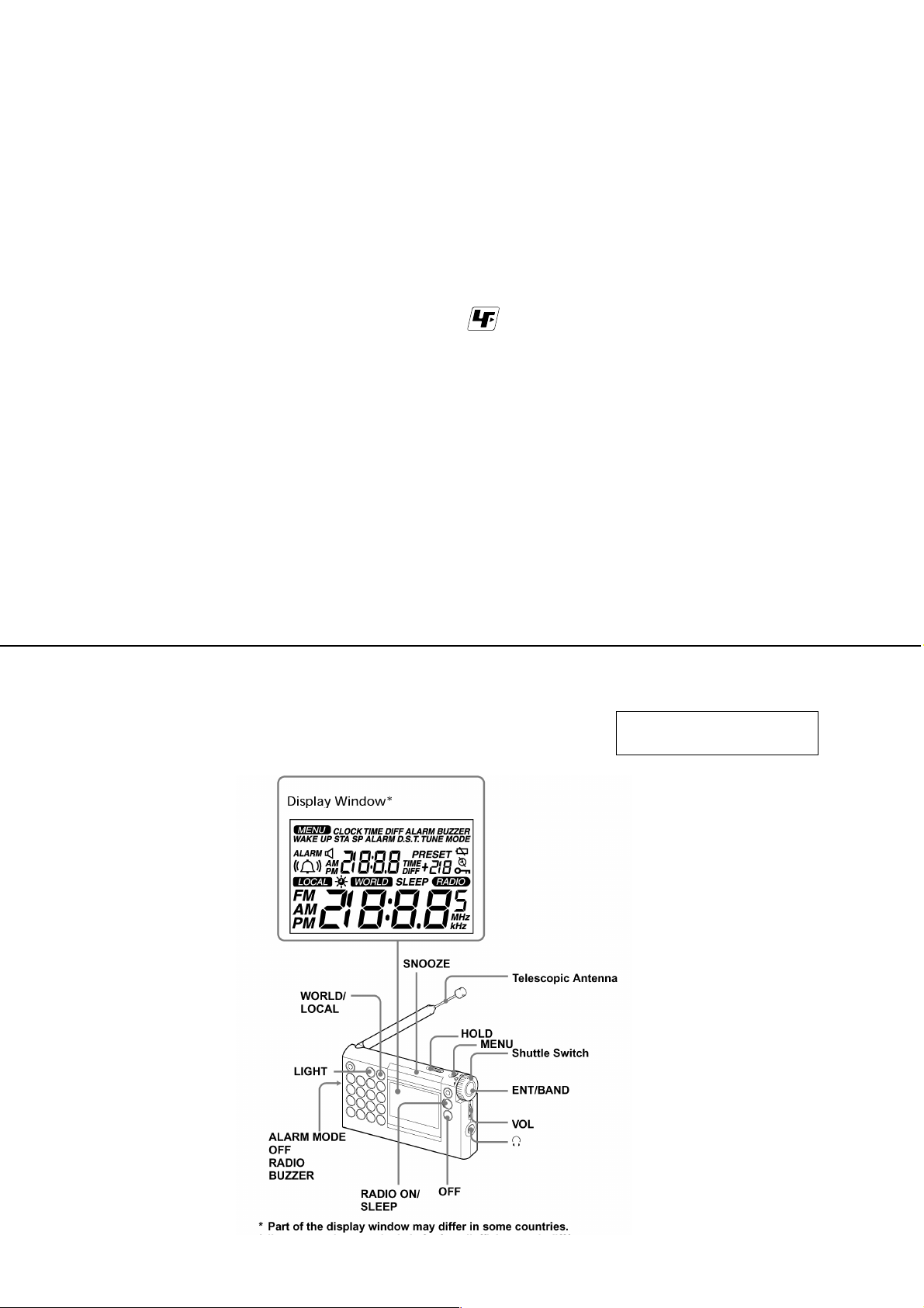
LOCATION AND FUNCTION OF CONTROLS
SECTION 1
GENERAL
This section is extracted from
instruction manual.
2
SECTION 2
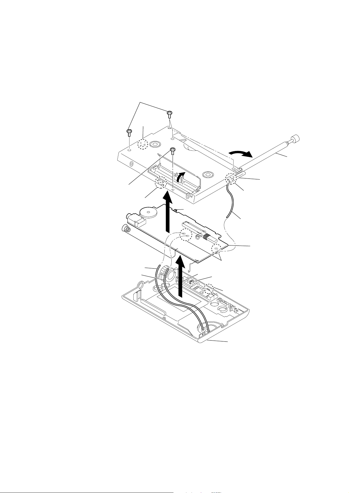
DISASSEMBLY
Note : Follow the disassembly procedure in the numerical order given.
2-1. MAIN BOARD
2
Screws (1.4X6 tapping)
5
Claw
3
4
Screws (1.4)
5
Claw
S301
• Caution during assembly
Align the hold switch(S301)
to the knob(HOLD).
6
ICF-C1200
1
ANT101
5
Red
Cabinet (rear) ASSY
Claw
Brown
Black
8
7
Remove solder
(three places)
Knob (HOLD)
5
Claw
Cabinet (front) ASSY
Main board
3
ICF-C1200
e
c
r
B
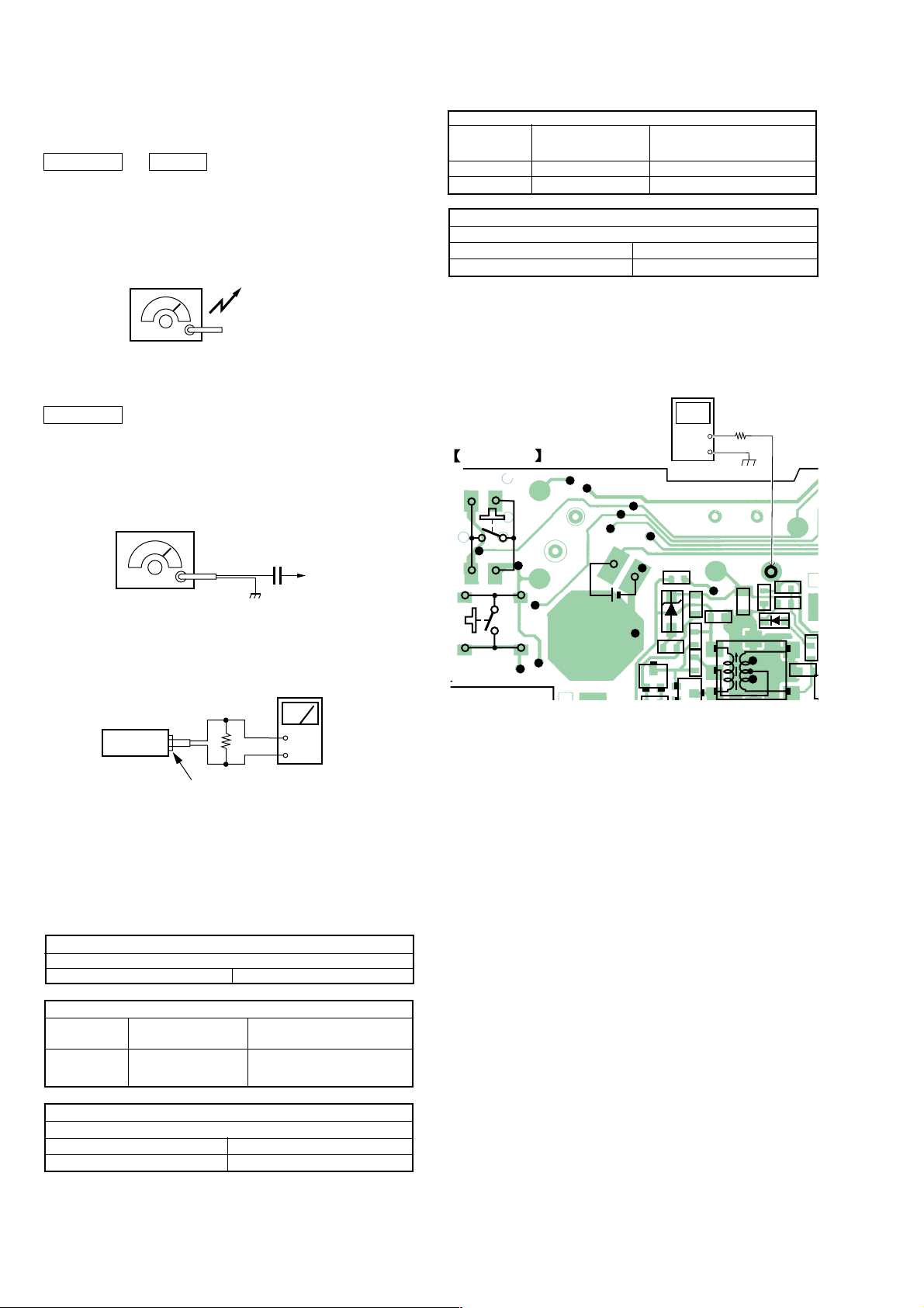
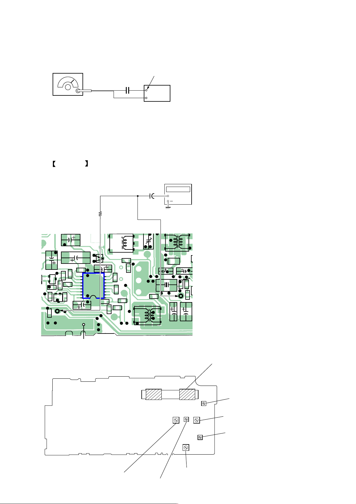
3-1.TUNER SECTION
AM Section
BAND button : AM
Volume : MIN
0dB=1µV
AM RF signal
generator
SECTION 3
ELECTRICAL ADJUSTMENTS
Adjust part Frequency display
Confirmation 87.5MHz 3.0 to 4.0V
Confirmation 108MHz 9.5 to 10.5V
Put the lead-wir
antenna close to
the set.
Frequency Coverage Adjustment
FM FREQUENCY COVERAGE CONFIRMATION
reading on digital
voltmeter
FM TRACKING ADJUSTMENT
Adjust for a maximum reading on level meter.
L103 87.5MHz
CT102 108MHz
30% amplitude modulation by 400Hz
signal.
Output level : as low as possible
FM Section
BAND button : FM
Volume : MIN
FM RF signal
generator
22.5kHz frequency deviation by
400Hz signal.
Output level : as low as possible
set
0.01 uF
32
Ω
J201 (phones)
level mete
+
–
telescopi
antenna
terminal
Connect Location :
MAIN BOARD (SIDE A)
S308
BAT401
PAS
Q402
BCE
Digital
voltmeter
R405
D403
R403
+
–
C407
R402
C406
CB
100K
C412
Ω
C404
T401
TP
(VT)
R314
C301
R315
TP
(VT)
D402
R401
C405
302
Adjustment Location : Main board (See page 5)
• Repeat the procedures in each adjustment several times, and the
frequency coverage and tracking adjustments should be finally
done by the trimmer capacitors.
Adjust for a maximum reading on level meter.
AM FREQUENCY COVERAGE ADJUSTMENT
AM IF ADJUSTMENT
T101 1485kHz <1480kHz>
Adjust part Frequency display
L105 531kHz <530kHz>
AM TRACKING ADJUSTMENT
Adjust for a maximum reading on level meter.
L 102 585kHz <580kHz>
< > : US model
reading on digital
voltmeter.
Adjustment value: 2.7V
Standaed value: 2.5 to 2.9V
CT101 1,485kHz <1,480kHz>
4
1-
C113
C108
CF101
L104
L101
C212
C202
C118
T101
C201
C207
C205
C103
C211
C214
C213
C206
C204
C410
R113
R129
R112
R202
R205
R201
R203
BCE
Q201
BCE
Q202
C210
C215
C208
C203
C209
C120
C122
D108
CT102
IC201
1
5
8
16
12
9
D109
TP
(3V)
TP
(76K)
VCO Adjustment
c
t
Procedure :
ICF-C1200
FM RF signal
generator
telescopi
antenna
terminal
µ
0.01 F
set
Carrier frequency : 98MHz
Modulation : No modulation
Output level : 1.38mV (–55dB)
1. Connect the frequency counter to TP (76k) and TP (3V) as shown
the figure below.
2. Turn the set to 98MHz.
3. Adjust RV101 for 76kHz reading frequency counter.
Standard value:75.5kHz to 76.5kHz.
MAIN BOARD (SIDE A)
frequency
counter
µ
F
1
+
33k
Ω
TP(3V)
+
TP1 (76k)
Adjustment Location:
[MAIN BOARD] (SIDE A)
L103: FM Tracking Adjustment
CT102: FM Tracking Adjustment
L102: AM Tracking Adjustment
CT101: AM Tracking Adjustment
L105: AM Frequvency Coverage Adjustmen
RV101: VCO Adjustment
T101: AM IF Adjustment
5
ICF-C1200
SECTION 4
DIAGRAMS
4-1. EXPLANATION OF IC TERMINALS
• IC301 TC9328AF-SR7491
(System control, LCD driver)
Pin No. Pin name I/O Description
1-4 COM1-4 O LCD common output.
5-26 S1-S22 O LCD segment output.
27 HOLD SW I HOLD switch input. ON:L OFF:H
28-30 KR1-3 I Key return input.
31 VDD — Power supply terminal.
32-34 KR1-3 O Key souce output.
35 POWER O Power ON control signal output. ON:L OFF:H
36 BEEP O Beep signal output.
37 MUTE O Mute signal output.
38 WAKE UP O Alarm output at volume control min. ON:L OFF:H
39 LCD I LCD check test mode setting input.
40 BAND O Band select signal output. AM:H FM:L
41 TEST — Not used (Fixed at "L").
42 HOLD — Not used (Fixed at "L").
43 INTR1 I 1.9V voltage detection terminal. Radio OFF :L
44 INTR2 I 1.1V voltage detection terminal. All OFF :L
45 — Not used (OPEN).
46 — Not used (OPEN).
47 GND — Ground terminal.
48 FM IN I FM local oscillator signal input.
49 AM IN I AM local oscillator signal input.
50 VDD — Power supply terminal.
51 D01 — Not used (OPEN).
52 D02 O Tuning voltage control output.
53 VREG — Regulator output for phase compalator.
54 — Not used (OPEN).
55 AL SW1 I ALARM switch input (OFF).
56 AL SW2 I ALARM switch input (RADIO).
57 AL SW3 I ALARM switch input (BUZZER).
58 VDET I 2.1V voltage detection input.
59 ID I Destination select input.
60 ID I Destination select input.
61 — Not used (OPEN).
62 SP BEEP O Beep signal output.
63 LIGHT O LCD back light ON/OFF output.
64 ST/MO O Stereo/Mono select output.
65-69 — Not used (OPEN).
70 RESET I Reset signal input.
71 XOUT O Oscillator output (75kHz).
72 XIN I Oscillator input (75kHz).
73 GND — Ground terminal.
74 VDB — Capacitor terminal.
75 C1 — Capacitor terminal.
76 C2 — Capacitor terminal.
77 VEE — Voltage pull-up terminal.
78 C3 — Capacitor terminal.
79 C4 — Capacitor terminal.
80 VLCD — Voltage pull-up terminal.
6
 Loading...