

Page 1
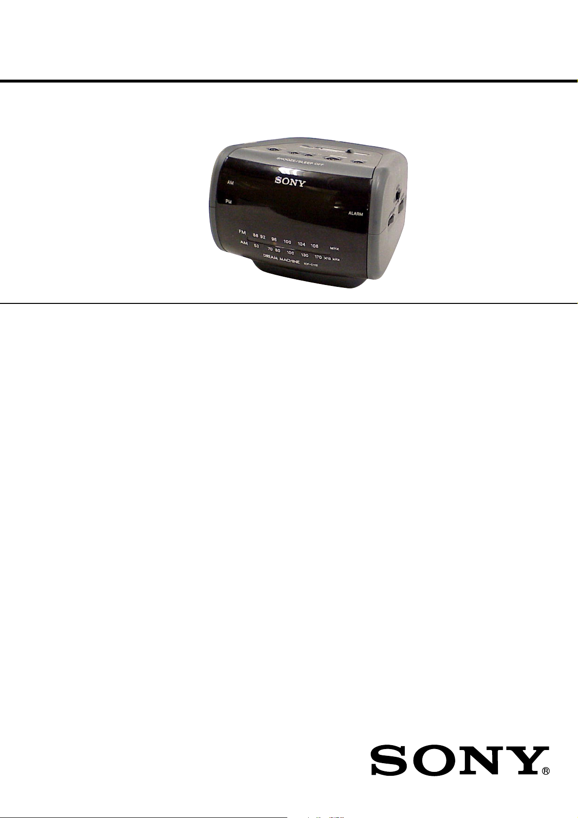
ICF-C112
SERVICE MANUAL
Ver 1.0 2003. 03
SPECIFICATIONS
Time display:
12-hour system
Frequency range:
FM: 87.5 - 108 MHz
AM: 530 - 1710 kHz
Speaker:
Approx. 6.6 cm (2 5/8 inches) dia., 8 ohm
Power output:
120 mW (at 10% harmonic distortion)
Power requirements:
120 V AC, 60 Hz
For the power backup function: 9 V DC, one 6F22 battery
Battery life:
Approx. 14 hours, using Sony 006P (6F22) battery
Dimensions:
Approx. 135 × 100 × 130 mm (w/h/d)
3/8 × 4 × 5 1/8 inches) incl. projecting parts and controls
(5
Mass:
Approx. 570 g (1 lb 4 oz) not incl. battery
Design and specifications are subject to change without notice.
E Model
9-877-123-01
2003C0400-1
© 2003. 03
FM/AM CLOCK RADIO
Sony Corporation
Personal Audio Company
Published by Sony Engineering Corporation
1
Page 2

ICF-C112
Notes on Chip Component Replacement
• Never reuse a disconnected chip component.
• Notice that the minus side of a tantalum capacitor may be dam-
aged by heat.
TABLE OF CONTENTS
1. SERVICING NOTES
1-1. Cord Dressing (Power Cord)............................................... 3
1-2. Pointer Alignment ............................................................... 3
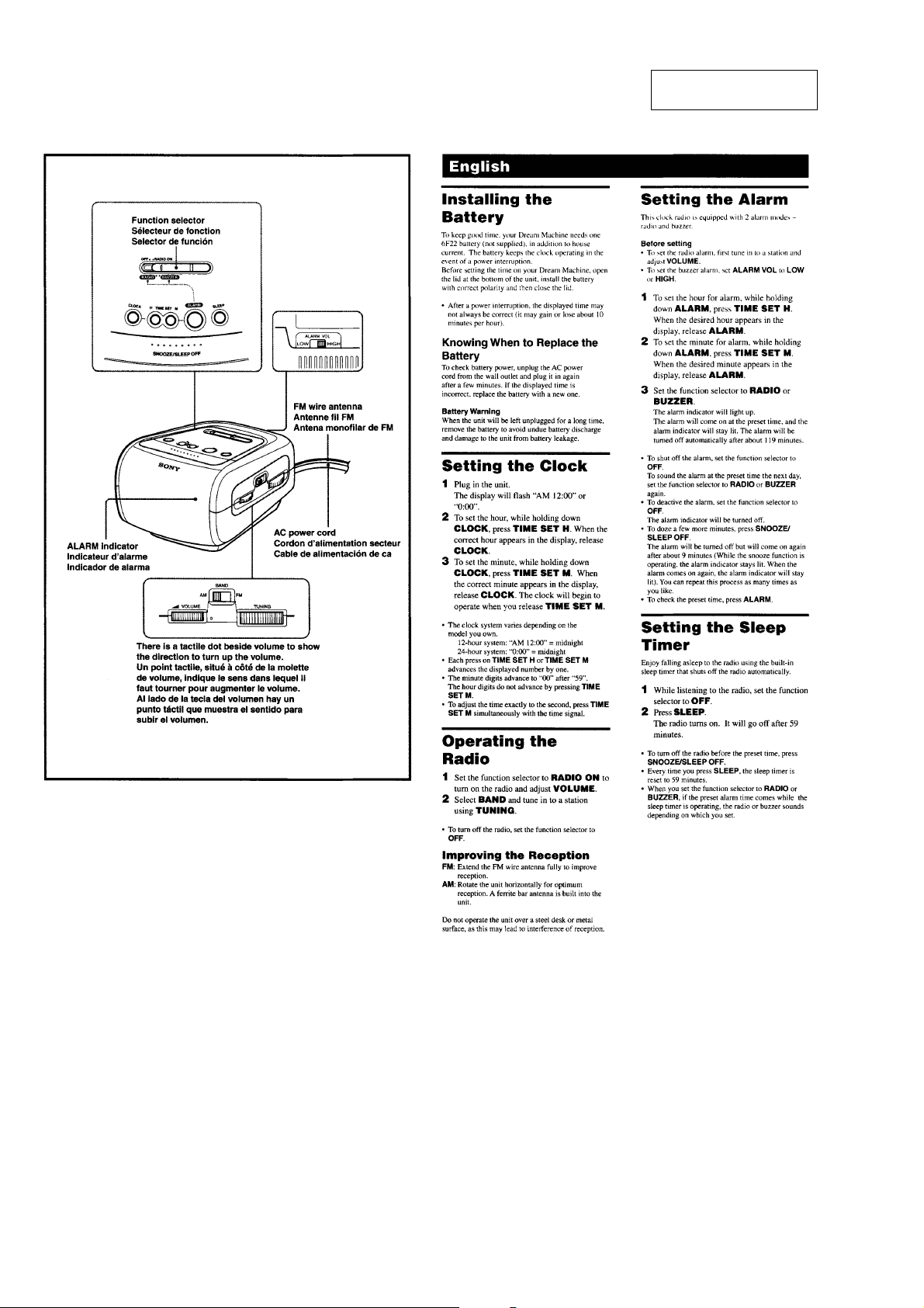
2. GENERAL
Installing the Battery ............................................................... 4
Setting the Clock ..................................................................... 4
Operating the Radio................................................................. 4
Setting the Alarm..................................................................... 4
Setting the Sleep Timer ........................................................... 4
3. DISASSEMBLY
3-1. Panel (Front)........................................................................5
3-2. Cabinet (Upper) Single Assy...............................................6
3-3. Main Board Section ............................................................ 6
3-4. Main Board, LED101, Switch Board .................................. 7
4. ELECTRICAL ADJUSTMENTS................................... 8
5. DIAGRAMS
5-1. Block Diagram .................................................................. 11
5-2. Printed Wiring Boards ....................................................... 12
5-3. Schematic Diagram ........................................................... 13
5-4. IC Block Diagrams............................................................ 14
6. EXPLODED VIEWS
6-1. Cabinet (Upper) Section.................................................... 15
6-2. Main Board Section .......................................................... 16
7. ELECTRICAL PARTS LIST ........................................ 17
SAFETY-RELATED COMPONENT W ARNING!!
COMPONENTS IDENTIFIED BY MARK 0 OR DOTTED LINE
WITH MARK 0 ON THE SCHEMATIC DIAGRAMS AND IN
THE PARTS LIST ARE CRITICAL TO SAFE OPERATION.
REPLACE THESE COMPONENTS WITH SONY P ARTS WHOSE
PART NUMBERS APPEAR AS SHOWN IN THIS MANUAL OR
IN SUPPLEMENTS PUBLISHED BY SONY.
2
Page 3
1-1. CORD DRESSING
d
(POWER CORD)
1) Set the power cord as shown in the figure.
2) Mount the chassis with power cord retainer
board and screws (P 3 × 10).
Note: Tighten completely the screws (P 3 × 10).
ICF-C112
SECTION 1
SERVICING NOTES
screw P 3x10
power cord retainer boar
power cord
1-2. POINTER ALIGNMENT
1
pointer
6
P 3x10
2
knob (tuning)
chassis
5
MAIN board
4
3
3
Page 4
ICF-C112
SECTION 2
GENERAL
This section is extracted
from instruction manual.
4
Page 5
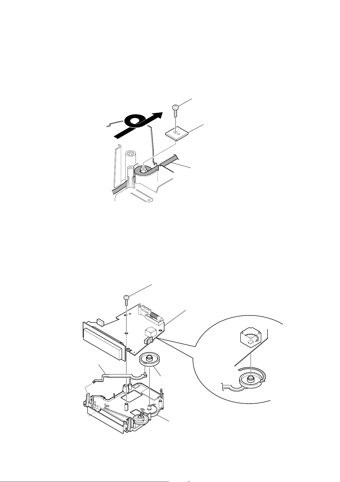
SECTION 3
DISASSEMBLY
Note : This set can be disassemble according to the following sequence.
SET
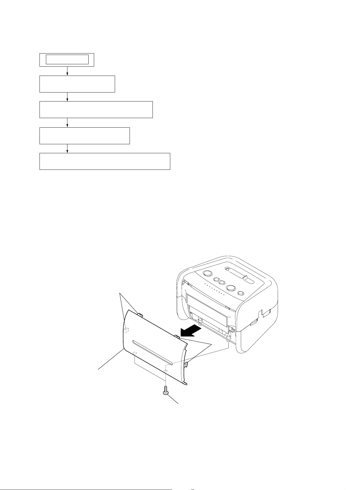
3-1. PANEL (FRONT)
(Page 5)
3-2. CABINET (UPPER) SINGLE ASSY
(Page 6)
3-3. MAIN BOARD SECTION
(Page 6)
3-4. MAIN BOARD, LED101, SWITCH BOARD
(Page 7)
ICF-C112
Note : Follow the disassembly procedure in the numerical order given.
3-1. P ANEL (FRONT)
claws
2
3
panel (front)
claws
1
P 2.6x8
5
Page 6
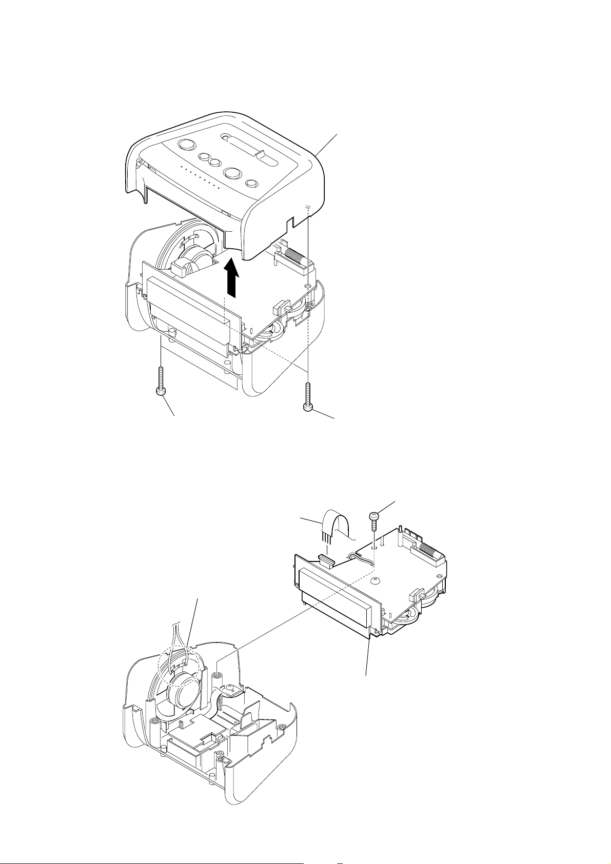
ICF-C112
y
3-2. CABINET (UPPER) SINGLE ASSY
3
cabinet (upper) single ass
4
3-3. MAIN BOARD SECTION
2
P 3x30
1
Removal the solders.
2
CN1
1
P 3x30
3
P 3x10
4
MAIN board section
6
Page 7

3-4. MAIN BOARD, LED101, SWITCH BOARD
d
7
Removal the solders.
5
4
P 3x10
claw
6
MAIN board
2
SWITCH boar
ICF-C112
8
LED101
claw
1
3
Removal the solders.
P 3x10
7
Page 8

ICF-C112
)
SECTION 4
ELECTRICAL ADJUSTMENTS
FM SECTION 0 dB = 1 µV
Setting:
BAND switch: FM
VOLUME control: MIN
FM RF signal
generator
0.01
400Hz, 30% FM modulation
frequency deviation
Output level: as low as possible
±
22.5kHz
AM SECTION
Setting:
BAND switch: AM
VOLUME control: MIN
AM RF signal
generator
400Hz, 30%
AM modulation
Output level: as low as possible
FM lead wire
antenna terminal
µ
F
set
Put the lead-wire
antenna close to
the set.
FM FREQUENCY COVERAGE ADJUSTMENT
Adjust for a maximum reading on level meter.
L2 CT6
86.5 MHz 109.5 MHz
FM TRACKING ADJUSTMENT
Adjust for a maximum reading on level meter.
L1 CT5
86.5 MHz 109.5 MHz
AM IF ADJUSTMENT
Adjust for a maximum reading on level meter.
T1
455 kHz
AM FREQUENCY COVERAGE ADJUSTMENT
Adjust for a maximum reading on level meter.
L3 CT4
515 kHz 1,750 kHz
AM TRACKING ADJUSTMENT
Adjust for a maximum reading on level meter.
L4 CT3
600 kHz 1,400 kHz
Adjustment Location: See page 9.
• Connecting Level Meter (FM and AM)
level meter
(range: 0.5–5 V ac
Ω
16
set
speaker terminal
Repeat the procedures in each adjustment several times, and the
frequency coverage and tracking adjustments should be finally done
by the trimmer capacitors.
8
Page 9

Adjustment Location:
G
LEAD WIRE
ANTENNA
(SPEAKER)
FM
SP1
SP1
ICF-C112
T1
AM IF
ADJ
L4
L2
L1
CT5
CT6
CT3
CT4
L3
RV1
T1
+
+
L4, CT3
AM
TRACKING
ADJ
TRACKIN
CV1
TUNING
S1
BAND
FM
AM
L3, CT4
AM FREQUENCY
COVERAGE ADJ
L1, CT5
FM
ADJ
L2, CT6
FM FREQUENCY
COVERAGE ADJ
9
Page 10

ICF-C112
THIS NOTE IS COMMON FOR PRINTED WIRING
BOARDS AND SCHEMATIC DIAGRAMS.
Common Note on Schematic Diagram:
• All capacitors are in µF unless otherwise noted. pF: µµF
50 WV or less are not indicated except for electrolytics
and tantalums.
• All resistors are in Ω and 1/
specified.
f
•
• C : panel designation.
Note: The components identified by mark 0 or dotted line
• A : B+ Line.
• H : adjustment for repair.
•Total current is measured with no-signal.
• Power voltage is dc 9V and fed with regulated dc power
•Voltage is dc with respect to ground under no-signal
•Voltages are taken with a VOM (Input impedance 10 MΩ).
• Signal path.
: internal component.
with mark 0 are critical for safety .
Replace only with part number specified.
supply from battery terminal.
(detuned) condition.
no mark : FM
(): AM
Voltage variations may be noted due to normal production tolerances.
F : FM
f : AM
4
W or less unless otherwise
SECTION 5
DIAGRAMS
Common Note on Printed Wiring Boards:
• X : parts extracted from the component side.
• Y : parts extracted from the conductor side.
f
•
• : Pattern from the side which enables seeing.
: internal component.
10
Page 11

5-1. BLOCK DIAGRAM
ICF-C112
FM
LEAD WIRE
ANTENNA
CT3,L4
AM
TRACKING
FREQUENCY
CT5,L1
FM
TRACKING
CT6,L2
FM
FREQUENCY
COVERAGE
FERRITE-ROD
CT4,L3
AM
COVERAGE
AM
ANTENNA
• Signal path
: FM
: AM
L1
L2
L4
L3
TUNING
LED DISPLAY
CV1-3 CT5
CV1-4 CT6
CV1-1 CT3
CV1-2 CT4
CV1
LED101
(12H)
16
BAND SW
FM ANT
13
FM RF
10 15
FM FRONT-ENDAM FRONT-END
FM OSC
8
AM ANT
11
AM OSC
6
+B
14
1-13
15,16
17
1
|
13
S1
BAND
FM
AM
MIX OUT
REG
9
VREG
OSC 1/25 or 1/30
DISPLAY
DECODER/
DRIVER
CF3
FM DISCRI
3
DISCRI
FM
DISCRIMINATOR
ALARM
DISP
19
S103
ALARM
FM
IF IN
18
AM
IF IN
17
FM/AM
FRONT-END
IF AMP,DET
IC101
ALARM CLOCK
S105
TIME SET
M
D114
IC1
CF2
T1
CF1
T1
AM IF
DISPLAY
CONTROL
SLEEP
INPUT
23 21 22 24
S108
SLEEP
FM IF
AM IF
ALARM TIME CTR
INPUT
CONTROL
MIN SET
DET OUT
S104
CLOCK
24 25
HOUR SET
S106
TIME SET
H
+B
RV1
w VOLUME
27
OUTPUT
CONTROL
SNOOZE INPUT
AF IN
AF POWER
AMP
Q302
RIPPLE
FILTER
SLEEP OUT
ALARM
ALARM OFF
S111
SNOOZE/SLEEP OFF
+B
5
VOL
S100
ALARM
VOL
HIGH
LOW
VDD
OUT
Q1
AF OUT
15
17
16
18
(Function Selector)
VREG
28
NF
4
+B
S101-1 S101-2
S101
BUZZER
RADIO
RADIO ON
ALARM
OFF
SWITCH
Q301
D302
D301 D111
D304
D112
SP1
(SPEAKER)
DRY BATTERY
"006P" 9V
(IEC DESIGNATION 6F22)
KEEP THE CORRECT
TIME DURING POWER
STOPPAGE
< BACK UP >
T301
POWER
TRANSFORMER
~
AC IN
11 11
Page 12

ICF-C112
5-2. PRINTED WIRING BOARDS • Refer to page 10 for Common Note on Printed Wiring Boards.
A
B
C
D
E
F
G
H
1
234567891011121314
MAIN BOARD
• Semiconductor
Location
L4
AM
FERRITE-ROD
ANTENNA
D1
D2
R14
C15
L1
C33
FM RF
C1
CV1 TUNING
CT3
CV1-1
BAND
RV1
VOLUME
CT4
S1
S1
FM
AM
JC1
Q1
B C E
RV1
CV1-3
C6
C32
C31
JW2
C9
R10
R5
I
CV1-2
CV1-4
AM OSC
D111
C118
C2
C3
CT5
CT6
R2
L3
S108
SLEEP
R4
R6
C12
R135
R137
C119
D112
BPF1
R8
L2
FM OSC
C5
C4
C17
R9
R11
JW104
15 28
14 1
C34
R136
CF3
R108
R3
C109
R109
R110
CF2
C18
R15
15 16
C14
IC1
C23
C24
C16
C27
130
JW5
S103
ALARM
IC101
R111
R112
R116
CF1
JW1
BUZZER RADIO RADIO ON OFF
C21
C28
R133
C116
C115
C104
C105
R117
R115
R114
R113
LED101 LED DISPLAY (12H)
T1
S101 (Function Selector)
ALARM
C22
C29
C26
TIME SET
M
S105
JW102
JW103
JC103
SNOOZE/
SLEEP OFF
C35
JW4
S111
C25
R13
-2
-1
RED
WHT
D114
S106
31
JC105
JW101
JW3
JW6
H
C304
JW7
RED
B C E
Q302
S104
CLOCK
D302
C301
D304
RED
WHT
CN1
D301
C302
Q301
BCE
R305
C306
C303
R303
117
R101
LEAD WIRE
GRY
BLK
RED
JW300
JW301
FM
ANTENNA
BATTERY
SNAP
DRY BATTERY
"006P" 9V
(IEC DESIGNATION 6F22)
KEEP THE CORRECT
TIME DURING POWER
STOPPAGE
<BACK UP>
SWITCH BOARD
LOW HIGH
SP1
(SPEAKER)
RED
14
1-686-755- (11)
S100
ALARM
VOL
RED
1
3
1-686-757- (11)
11
11
TRANSFORMER BOARD
14
RED
T301
POWER TRANSFORMER
Ref. No. Location
D1 B-8
D2 B-8
D111 I-3
D112 I-3
D114 G-7
D301 H-9
D302 I-8
D304 D-9
IC1 D-5
IC101 H-5
LED101 I-6
Q1 H-2
Q301 D-8
Q302 E-8
1-686-756-
11
(11)
~ AC IN
J
1212
Page 13

5-3. SCHEMATIC DIAGRAM • Refer to page 10 for Common Note on Schematic Diagram and page 14 for IC Block Diagrams.
ICF-C112
LED101
JW7
L4
BPF1
D2D1
S1
JW1
C18
C1
IC1
IC B/D
R14 R15
T1
CT3
L1
CV1-1
CF2CF1
CT5
C3
C2
R8
C21 C22
L2
C14
R3
C4
C5
C33
C15
C23
C35
C6
Q1
JW5
C12
R4
JC1
R6
C31
C32
C9
IC101
JC105
R101
JC103
R108
R109
R110
R111
R112
IC B/D
S101
JW6
JW4
R11
JW103
JW102
C109
JW104
D114
S105 S106
S108 S111
S104S103
R133
C116
C115
C105
R117
C104
R136
R113
R114
R115
R116
R135 R137
C118 C119
D111 D112
CF3
L3
RV1
CT4
CV1-2CV1-4CV1-3
R5R10
C34
R2
CT6
JW2
R9
C17
C16
C26
C24
C25
C27
C29 C28
S100
SP1
JW3
R13
C306
Q302
R305
D304
Q301
JW101
C303
R303
C304
C302
D302
C301
D301
T301
CN1
JW301
JW300
13 13
Page 14

ICF-C112
5-4. IC BLOCK DIAGRAMS
IC1 CXA1019S
GND
GND
AF OUT+BRIPPLE
FILTER
AF IN
DET OUT
23 22 21 202425 19 18 17 1629 28 27 2630
AFC (J)AGC
AFC (W)AGC
IF GND
LED
NC
FM IF IN
AM IF IN
BAND SW
AM IF DET AGC
AF POWER AMP AM FE FM IF
FM
DISCRIMINATOR
FM FE
2 345 6 7 8 9
1
GND
GND
DISCRI
NF
VOL
AM OSC
AFC
FM OSC
REG
10
TUNING
METER
FM RF
11
AM ANT
15141312
NC
FE GND
FM ANT
MIX OUT
IC101 LM8560N
12/24 HR
SELECT
28 27 26 25 24 23 22 21 20 19 18 17 16 15
CR/INPUT
OSC
50/60 Hz
SELECT
50/60 Hz
INPUT
SLEEP
INPUT
SNOOZE
INPUT
D
HOUR SET
MIN SET
D DD D D
VSS
ALARM
DISP
ALARM
OFF
SLEEP OUT
ALARM OUT
VDD
CTR
STAND
BY DET
BLANK &
PF.
DET
GATE
50/60Hz
1/25 or 1/30
2Hz
1/2
1Hz
SEC
FLASH
CTR
GATE
1 2 3 4 5 6 7 8 9 10 11 12 13 14
S
,
S HR B
,
AM & 10
HR AG & DE
PM & 10
ALARM
MIN CTR
COMPARATOR SLEEP CTR
TIME
MIN CTR
HR B & G
S HR C & HR B
,
10
ALARM
HR CTR
HR CTR
OUTPUT DECODER/DRIVER
HR A & F
HR C & D
RESET
CONTROL
F.SAMPLE
TIME
S MIN A & F
,
10
INPUT
CONTROL
S MIN B & G
,
,
10
DISPLAY
CONTROL
S.SAMPLE
S MIN E
& MIN E
,
10
S MIN C & D
10
PWR UP
OUTPUT
CONTROL
CONTROL
MIN C & D
MIN B & G
MIN A & F
SLEEP
SEC,TIME,ALARM
COLON OUTPUT
1414
Page 15

NOTE:
• The mechanical parts with no reference
number in the exploded views are not supplied.
• Items marked “*” are not stocked since
they are seldom required for routine service.
Some delay should be anticipated
when ordering these items.
6-1. CABINET (UPPER) SECTION
SECTION 6
EXPLODED VIEWS
• Color Indication of Appearance Parts
Example :
KNOB, BALANCE (WHITE) ... (RED)
R
Parts Color Cabinet’s Color
• Accessories are given in the last of this parts
list.
R
ICF-C112
The components identified by
mark 0 or dotted line with mark
0 are critical for safety.
Replace only with part number
specified.
3
2
1
4
#2
#1
#2
Ref. No. Part No. Description Remark
13-369-135-21 LID, BATTERY CASE
2 X-3383-416-1 CABINET (UPPER) SINGLE ASSY
(BLACK)...(BLACK)
2 X-3383-417-1 CABINET (UPPER) SINGLE ASSY
(WHITE)...(WHITE)
Ref. No. Part No. Description Remark
3 3-246-791-01 KNOB (FUNCTION) (BLACK)...(BLACK)
3 3-246-791-11 KNOB (FUNCTION) (WHITE)...(WHITE)
4 3-246-788-01 PANEL (FRONT)
#1 7-685-134-19 SCREW +P 2.6X8 TYPE2 NON-SLIT
#2 7-685-153-19 SCREW +P 3X30 TYPE2 NON-SLIT
15
Page 16

ICF-C112
)
6-2. MAIN BOARD SECTION
#3
#3
L4
56
SP1
62
55
57
not supplied
61
58
#3
LED101
#3
60
#3
not supplied
(POWER CORD RETAINER board)
54
59
59
not supplied
(SWITCH board
51
52
T301
53
The components identified by
mark 0 or dotted line with mark
0 are critical for safety.
Replace only with part number
specified.
Ref. No. Part No. Description Remark Ref. No. Part No. Description Remark
51 3-919-268-01 KNOB (VOL) (BLACK)...(BLACK)
51 3-919-268-11 KNOB (VOL) (WHITE)...(WHITE)
52 3-246-784-01 CABINET (LOWER) (BLACK)...(BLACK)
52 3-246-784-11 CABINET (LOWER) (WHITE)...(WHITE)
53 3-246-344-11 FOOT, RUBBER
0 54 1-769-339-22 CORD, POWER
* 55 A-3347-218-A MAIN BOARD, COMPLETE (BLACK)
* 55 A-3663-993-A MAIN BOARD, COMPLETE (WHITE)
56 3-226-590-01 HOLDER (ANTENNA)
57 1-535-804-71 SNAP, BATTERY
58 1-754-135-11 ANTENNA (WIRE)
59 3-553-567-00 CUSHION
60 3-246-786-01 KNOB (TUNING) (BLACK)...(BLACK)
60 3-246-786-11 KNOB (TUNING) (WHITE)...(WHITE)
61 3-246-787-01 POINTER
62 A-3347-348-A TRANSFORMER BOARD, COMPLETE
L4 1-419-532-41 COIL, FERRITE-ROD ANTENNA (AM)
LED101 6-500-504-01 LED COG509T0A1
SP1 1-529-456-13 SPEAKER (6.6cm)
0 T301 1-433-573-21 TRANSFORMER, POWER
#3 7-685-647-79 SCREW +P 3X10 TYPE2 NON-SLIT
16
Page 17

ICF-C112
SECTION 7
ELECTRICAL PARTS LIST
NOTE:
• Due to standardization, replacements in
the parts list may be different from the
parts specified in the diagrams or the
components used on the set.
• RESISTORS
All resistors are in ohms.
METAL:Metal-film resistor.
METAL OXIDE: Metal oxide-film resistor.
F:nonflammable
Ref. No. Part No. Description Remark Ref. No. Part No. Description Remark
* A-3347-218-A MAIN BOARD, COMPLETE (BLACK)
* A-3663-993-A MAIN BOARD, COMPLETE (WHITE)
*********************
1-535-804-71 SNAP, BATTERY
1-754-135-11 ANTENNA (WIRE)
3-226-590-01 HOLDER (ANTENNA)
7-685-647-79 SCREW +P 3X10 TYPE2 NON-SLIT
• Items marked “*” are not stocked since
they are seldom required for routine service.
Some delay should be anticipated
when ordering these items.
• SEMICONDUCTORS
In each case, u : µ, for example:
uA.. : µA.. uPA.. : µPA..
uPB.. : µPB.. uPC.. : µPC.. uPD.. : µPD..
• CAPACITORS
uF : µF
• COILS
uH : µH
C118 1-162-970-11 CERAMIC CHIP 0.01uF 10% 25V
C119 1-162-970-11 CERAMIC CHIP 0.01uF 10% 25V
C301 1-162-970-11 CERAMIC CHIP 0.01uF 10% 25V
C302 1-162-970-11 CERAMIC CHIP 0.01uF 10% 25V
C303 1-126-935-11 ELECT 470uF 20% 10V
C304 1-126-934-11 ELECT 220uF 20% 16V
C306 1-126-934-11 ELECT 220uF 20% 10V
The components identified by
mark 0 or dotted line with mark
0 are critical for safety.
Replace only with part number
specified.
When indicating parts by reference
number, please include the board.
MAIN
< BPF >
BPF1 1-236-022-11 FILTER, BAND PASS
< CAPACITOR >
C1 1-162-907-11 CERAMIC CHIP 2PF 0.25PF 50V
C2 1-162-915-11 CERAMIC CHIP 10PF 0.5PF 50V
C3 1-162-915-11 CERAMIC CHIP 10PF 0.5PF 50V
C4 1-162-997-11 CERAMIC CHIP 10PF 0.5PF 50V
C5 1-162-918-11 CERAMIC CHIP 18PF 5% 50V
C6 1-162-934-11 CERAMIC CHIP 3PF 0.25PF 50V
C9 1-162-927-11 CERAMIC CHIP 100PF 5% 50V
C12 1-162-970-11 CERAMIC CHIP 0.01uF 10% 25V
C14 1-107-826-11 CERAMIC CHIP 0.1uF 10% 16V
C15 1-126-947-11 ELECT 47uF 20% 10V
C16 1-162-970-11 CERAMIC CHIP 0.01uF 10% 25V
C17 1-126-960-11 ELECT 1uF 20% 50V
C18 1-162-970-11 CERAMIC CHIP 0.01uF 10% 25V
C21 1-126-963-11 ELECT 4.7uF 20% 50V
C22 1-126-964-11 ELECT 10uF 20% 50V
C23 1-164-227-11 CERAMIC CHIP 0.022uF 10% 25V
C24 1-107-826-11 CERAMIC CHIP 0.1uF 10% 16V
C25 1-126-964-11 ELECT 10uF 20% 50V
C26 1-126-935-11 ELECT 470uF 20% 10V
C27 1-115-156-11 CERAMIC CHIP 1uF 10V
C28 1-115-156-11 CERAMIC CHIP 1uF 10V
C29 1-104-665-11 ELECT 100uF 20% 10V
C31 1-107-826-11 CERAMIC CHIP 0.1uF 10% 16V
C32 1-162-927-11 CERAMIC CHIP 100PF 5% 50V
C33 1-162-964-11 CERAMIC CHIP 0.001uF 10% 50V
C34 1-162-927-11 CERAMIC CHIP 100PF 5% 50V
C35 1-162-964-11 CERAMIC CHIP 0.001uF 10% 50V
C104 1-162-968-11 CERAMIC CHIP 0.0047uF 10% 50V
C105 1-162-966-11 CERAMIC CHIP 0.0022uF 10% 50V
C109 1-165-176-11 CERAMIC CHIP 0.047uF 10% 16V
C115 1-162-970-11 CERAMIC CHIP 0.01uF 10% 25V
C116 1-162-970-11 CERAMIC CHIP 0.01uF 10% 25V
< FILTER >
CF1 1-781-790-11 FILTER, AM CERAMIC
CF2 1-781-861-71 FILTER, CERAMIC (COMBINATION)
CF3 1-781-861-71 FILTER, CERAMIC (COMBINATION)
< CONNECTOR >
* CN1 1-568-270-11 SOCKET, CONNECTOR 4P
< VARIABLE CAPACITOR >
CT3-6 1-141-620-11 CAP, VAR
CV1 1-141-620-11 CAP, VAR (TUNING)
< DIODE >
D1 8-719-911-19 DIODE 1SS119-25
D2 8-719-911-19 DIODE 1SS119-25
D111 8-719-911-19 DIODE 1SS119-25
D112 8-719-911-19 DIODE 1SS119-25
D114 8-719-911-19 DIODE 1SS119-25
D301 8-719-052-88 DIODE 1N4002
D302 8-719-911-19 DIODE 1SS119-25
D304 8-719-911-19 DIODE 1SS119-25
< IC >
IC1 8-752-037-02 IC CXA1019S
IC101 8-759-821-46 IC LM8560N
< JUMPER RESISTOR >
JC1 1-216-864-11 METAL CHIP 0 5% 1/10W
JC103 1-216-864-11 METAL CHIP 0 5% 1/10W
JC105 1-216-864-11 METAL CHIP 0 5% 1/10W
< COIL >
* L1 1-422-320-11 COIL, AIR-CORE
L2 1-422-131-00 COIL, FM OSCILLATION
L3 1-419-533-21 COIL, OSCILLATION (AM)
L4 1-419-532-41 COIL, FERRITE-ROD ANTENNA (AM)
17
Page 18

ICF-C112
MAIN TRANSFORMERSWITCH
Ref. No. Part No. Description Remark Ref. No. Part No. Description Remark
< DIODE >
LED101 6-500-504-01 LED COG509T0A1
< TRANSISTOR >
Q1 8-729-026-52 TRANSISTOR 2SA1576A-T106-R
Q301 8-729-026-52 TRANSISTOR 2SA1576A-T106-R
Q302 8-729-011-92 TRANSISTOR 2SC2001TP-K1K2
< RESISTOR >
S100 1-692-181-21 SWITCH, SLIDE (ALARM VOL) (BLACK)
S100 1-692-181-51 SWITCH, SLIDE (ALARM VOL) (WHITE)
*************************************************************
A-3347-348-A TRANSFORMER BOARD, COMPLETE
SWITCH BOARD
*************
< SWITCH >
******************************
R2 1-216-829-11 METAL CHIP 4.7K 5% 1/10W
R3 1-216-801-11 METAL CHIP 22 5% 1/10W
R4 1-216-845-11 METAL CHIP 100K 5% 1/10W
R5 1-216-833-11 METAL CHIP 10K 5% 1/10W
R6 1-216-841-11 METAL CHIP 47K 5% 1/10W
R8 1-216-821-11 METAL CHIP 1K 5% 1/10W
R9 1-216-805-11 METAL CHIP 47 5% 1/10W
R10 1-216-837-11 METAL CHIP 22K 5% 1/10W
R11 1-216-829-11 METAL CHIP 4.7K 5% 1/10W
R13 1-216-833-11 METAL CHIP 10K 5% 1/10W
R14 1-216-825-11 METAL CHIP 2.2K 5% 1/10W
R15 1-216-817-11 METAL CHIP 470 5% 1/10W
R101 1-216-805-11 METAL CHIP 47 5% 1/10W
R108 1-216-845-11 METAL CHIP 100K 5% 1/10W
R109 1-216-845-11 METAL CHIP 100K 5% 1/10W
R110 1-216-845-11 METAL CHIP 100K 5% 1/10W
R111 1-216-845-11 METAL CHIP 100K 5% 1/10W
R112 1-216-845-11 METAL CHIP 100K 5% 1/10W
R113 1-216-845-11 METAL CHIP 100K 5% 1/10W
R114 1-216-845-11 METAL CHIP 100K 5% 1/10W
R115 1-216-845-11 METAL CHIP 100K 5% 1/10W
R116 1-216-845-11 METAL CHIP 100K 5% 1/10W
R117 1-216-849-11 METAL CHIP 220K 5% 1/10W
R133 1-216-845-11 METAL CHIP 100K 5% 1/10W
R135 1-249-389-11 CARBON 4.7 5% 1/4W
0 1-769-339-22 CORD, POWER
< TRANSFORMER >
0 T301 1-433-573-21 TRANSFORMER, POWER
*************************************************************
MISCELLANEOUS
***************
SP1 1-529-456-13 SPEAKER (6.6cm)
*************************************************************
ACCESSORIES
************
3-247-335-11 MANUAL, INSTRUCTION (ENGLISH,FRENCH,
SPANISH)
R136 1-216-801-11 METAL CHIP 22 5% 1/10W
R137 1-249-389-11 CARBON 4.7 5% 1/4W
R303 1-247-807-31 CARBON 100 5% 1/4W
R305 1-216-821-11 METAL CHIP 1K 5% 1/10W
< VARIABLE RESISTOR >
RV1 1-228-790-00 RES, VAR, CARBON 50K (VOLUME)
< SWITCH >
S1 1-692-181-21 SWITCH, SLIDE (BAND) (BLACK)
S1 1-692-181-51 SWITCH, SLIDE (BAND) (WHITE)
S101 1-771-904-11 SWITCH, SLIDE (Function Selector)
S103 1-771-550-11 SWITCH, TACTILE (ALARM)
S104 1-771-550-11 SWITCH, TACTILE (CLOCK)
S105 1-771-550-11 SWITCH, TACTILE (TIME SET M)
S106 1-771-550-11 SWITCH, TACTILE (TIME SET H)
S108 1-771-550-11 SWITCH, TACTILE (SLEEP)
S111 1-554-937-11 SWITCH, TACTILE (SNOOZE/SLEEP OFF)
< TRANSFORMER >
T1 1-435-399-21 TRANSFORMER, IF
*************************************************************
18
The components identified by
mark 0 or dotted line with mark
0 are critical for safety.
Replace only with part number
specified.
Page 19

MEMO
ICF-C112
19
Page 20

ICF-C112
REVISION HISTOR Y
Clicking the version allows you to jump to the revised page.
Also, clicking the version at the upper right on the revised page allows you to jump to the next revised
page.
Ver. Date Description of Revision
1.0 2003. 03 New
20
 Loading...