

Page 1
ICD-B16/B26
SERVICE MANUAL
Ver 1.0 2004.03
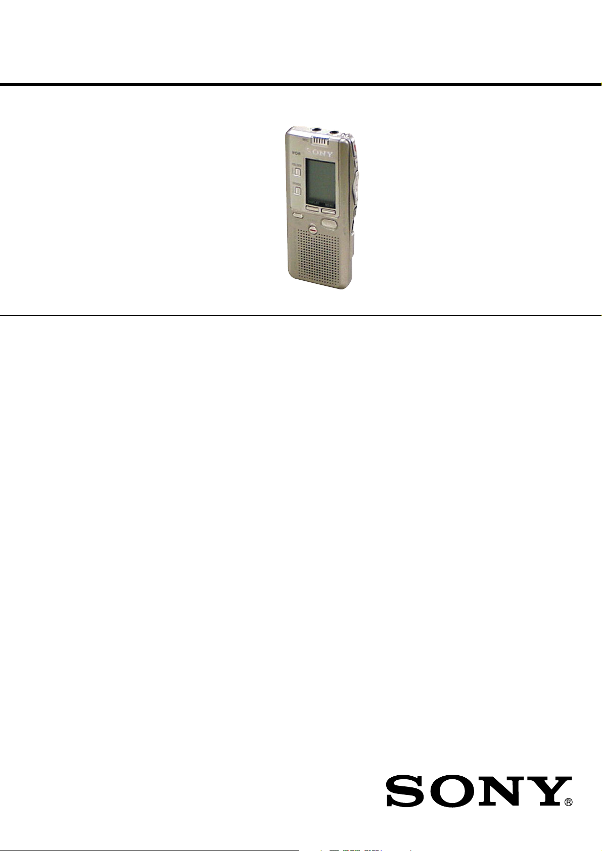
Photo: ICD-B26
SPECIFICATIONS
Recording media Built-in flash memory, Monaural recording
Recording time ICD-B16:
SP: 5 hours
LP: 8 hours 15 minutes
ICD-B26:
SP: 10 hours
LP: 16 hours 25 minutes
Frequency range 160 Hz - 3,300 Hz
Speaker approx. 3.2 cm (1 5/16 in.) dia.
Power output 250 mW
Input/Output • Earphone jack (minijack) for 8 - 300 ohms
ear receiver/headphones
• Microphone jack (minijack, monaural)
Plug in power
Minimum input level 0.6 mV
3 kilohms or lower impedance microphone
Power requirements Tw o LR03 (size AAA) alkaline batter ies: 3 V DC
Dimensions (w/h/d) (not incl. projecting parts and controls)
44.5 × 105.3 × 14.0 mm (1 13/16 × 4 1/4 × 9/16 in.)
Mass (incl. batteries) 69 g (2.5 oz)
Supplied accessories LR03 (size AAA) alkaline batteries (2) (For the
US only)
US Model
ICD-B26
AEP Model
Tourist Model
ICD-B16/B26
9-877-648-01
2004C04-1
© 2004.03
Design and specifications are subject to change without notice.
IC RECORDER
Sony Corporation
Personal Audio Company
Published by Sony Engineering Corporation
1
Page 2

ICD-B16/B26
Notes on Chip Component Replacement
• Never reuse a disconnected chip component.
• Notice that the minus side of a tantalum capacitor may be dam-
aged by heat.
UNLEADED SOLDER
•
Boards requiring use of unleaded solder are printed with the leadfree mark (LF) indicating the solder contains no lead.
(Caution: Some printed circuit boards may not come printed with
the lead free mark due to their particular size.)
: LEAD FREE MARK
Unleaded solder has the following characteristics.
• Unleaded solder melts at a temperature about 40°C higher than
ordinary solder.
Ordinary soldering irons can be used but the iron tip has to be
applied to the solder joint for a slightly longer time.
Soldering irons using a temperature regulator should be set to
about 350°C.
Caution: The printed pattern (copper foil) may peel away if
the heated tip is applied for too long, so be careful!
• Strong viscosity
Unleaded solder is more viscous (sticky, less prone to flow)
than ordinary solder so use caution not to let solder bridges
occur such as on IC pins, etc.
• Usable with ordinary solder
It is best to use only unleaded solder but unleaded solder may
also be added to ordinary solder.
TABLE OF CONTENTS
1. SERVICE NOTE ................................................................3
2. GENERAL
Index to Parts and Controls ..................................................... 4
3. DISASSEMBLY
3-1. Case (Upper) Assy .............................................................. 5
3-2. F-SW Board, P-SW Board .................................................. 6
3-3. Main Board ......................................................................... 6
4. DIAGRAMS
4-1. IC Pin Description............................................................... 7
4-2. Block Diagram .................................................................... 9
4-3. Printed Wiring Board – Main Section – ............................ 11
4-4. Printed Wiring Board – F-SW Section – ........................... 12
4-5. Printed Wiring Board – P-SW Section – ........................... 13
4-6. Schematic Diagram – Main Section –............................... 14
4-7. IC Block Diagrams............................................................ 15
5. EXPLODED VIEWS
5-1. Case Section ...................................................................... 16
5-2. Main Board Section .......................................................... 17
6. ELECTRICAL PARTS LIST ........................................ 18
2
Page 3
SECTION 1
C
SERVICE NOTE
1-1. CAUTIONS OF FLASH MEMORY (IC701)
EXCHANGE
[Precaution when the flash memory (IC701) is replaced]
When the flash memory (IC701) is replaced, be sure to perform the
BAD BLOCK check* and writing of the model code. If they are not
completed, the unit will not operate normally.
* BAD BLOCK check is to check the flash ROM memory
area (the BAD BLOCK area) where data cannot be
guaranteed. The resultant information of this check is stored
in the TOC-AREA so that the BAD BLOCK area should
not be used.
[BAD BLOCK Check Procedure]
1. When the power is turned on after the flash memory (IC701) is
replaced, the BAD BLOCK check starts automatically and the
OPR (D701) lights in orange.
2. In about 30 seconds after start of the check, the OPR (D701)
changes the color to green indicating that the check is
completed.
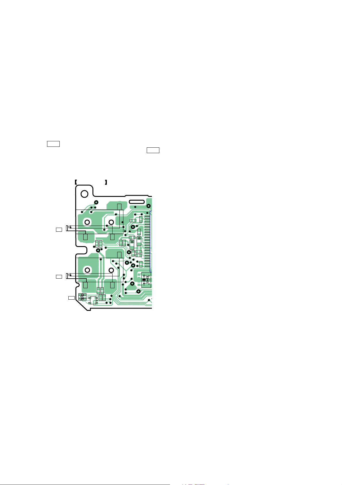
ICD-B16/B26
J101
MIC
(PLUG IN POWER)
J102
EAR
MAIN BOARD (SIDE A)
TP101
FB101
FB102
TP106
D701
OPR
RED(REC)
GRN
(PLAY)
Q701
CCB
FB104
—2
R727
E
—1
B
FB103
R726
R102
TP110
TP102
R103
TP708
R135
R104
TP702
C103
C101
TP107
C106
C105
TP701
TP501
C129
C104
C128
C120
X101
30
31
50
51
3
Page 4
ICD-B16/B26
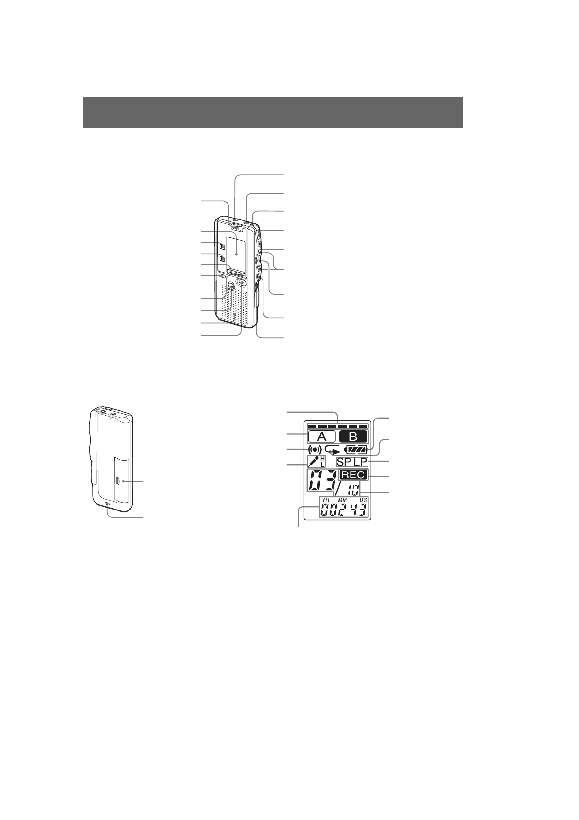
Index to Parts and Controls
Main unit
(built-in microphone)
MIC
SECTION 2
GENERAL
MIC jack
(PLUG IN POWER)
EAR (earphone) jack
OPR (operation) indicator
This section is extracted
from instruction manual.
Rear
Display window
FOLDER
DIVIDE
DISPLAY
MIC SENS
(microphone sensitivity)
MENU
ERASE
Speaker
STOP
Battery
compartment
Hook for handstrap
(not supplied)
Display window
Remaining memory indicator
Folder indication
Alarm indicator
Microphone sensitivity
indication
Counter /Remaining time indication /Recording date
indication /Current time indication (15:30, etc.) /Menu
indication (ALARM, BEEP, etc.) /Messages (ERASE, HOLD,
etc.)
zREC (record) /STOP
X PAUSE
– .REVIEW/
>+CUE
NxPLAY/STOP•
EXECUTE
HOLD
VOL (volume)
Remaining battery
indicator
Repeat play indicator
Recording mode
indication
REC (recording)
indicator
Selected message
number/Mode
indication of the
menu (ON, OFF, etc.)
4
Page 5
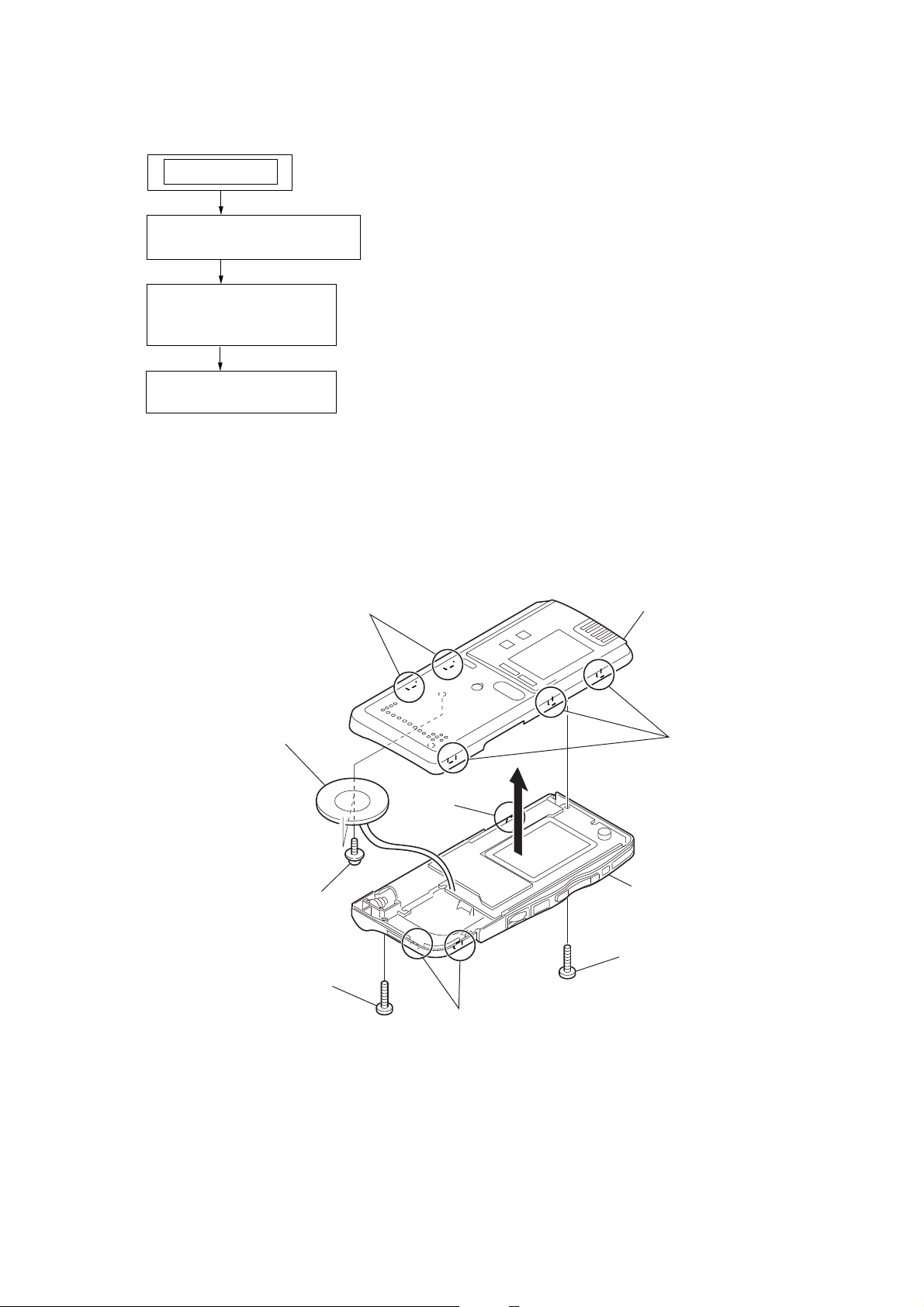
SECTION 3
y
DISASSEMBLY
Note : This set can be disassemble according to the following sequence.
SET
3-1. CASE (UPPER) ASSY
(Page 5)
3-2. F-SW BOARD,
P-SW BOARD
(Page 6)
3-3. MAIN BOARD
(Page 6)
Note : Follow the disassembly procedure in the numerical order given.
ICD-B16/B26
3-1. CASE (UPPER) ASSY
9
speaker (SP101)
8
two
(1.7
2
(B 1.7x7)
screws
x
2.5)
screw
3
two claws
6
claw
4
two claws
7
0
case (upper) ass
5
three claws
case block assy
1
screw
(B 1.7x10)
5
Page 6
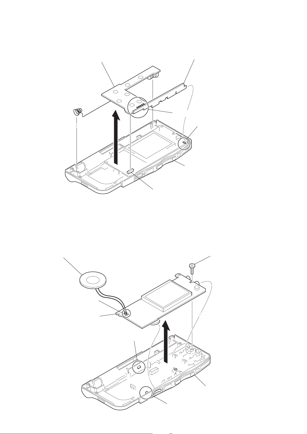
ICD-B16/B26
3-2. F-SW BOARD, P-SW BOARD
6
F-SW board
5
P-SW board
3-3. MAIN BOARD
speaker (SP101)
2
3
2
CN701
4
Removal the five solders.
1
Removal the solder.
case block assy
3
(1.7x4)
screw
1
Removal the two solders.
7
MAIN board
4
claw
5
6
case (lower) assy
claw
6
Page 7
ICD-B16/B26
SECTION 4
DIAGRAMS
4-1. IC PIN DESCRIPTION
• IC703 µPD780308GC-A71-8EU (MEMORY CONTROL, SYSTEM CONTROL)
Pin No. Pin Name I/O Pin Description
1 – 3 KEY0 – KEY2 I Key signal input
4 XHOLD I Hold switch signal input
5 AMPPOW O Power down control signal output to the power amplifier IC (IC103)
6AVREFON I A/D reference voltage input
7 XFMCE O Chip enable signal output to the flash memory IC (IC701)
8 VDD0 — Power supply pin (+3.3 V)
9AVREF — A/D reference voltage
10 XFMWE O Write enable signal output to the flash memory IC (IC701)
11 XFMALE O ALE signal output to the flash memory IC (IC701)
12 VSS1 — Ground pin
13 XFMR/B I Ready/Busy signal input from the flash memory IC (IC701)
14 XFMCLE O CLE signal output to the flash memory IC (IC701)
15, 16 NC O Not used. (Open)
17 XFMRE O Read enable signal output to the flash memory IC (IC701)
18 XFMSE O SE signal output to the flash memory IC (IC701)
19 XFMWP O WP signal output to the flash memory IC (IC701)
20 CLKOUT O Not used in this set. (Open)
21 BEEP O Beep signal output (2.4 kHz)
22 LIGHT O LCD back light control output Not used in this set. (Open)
23 to 26 COM0 to COM3 O LCD common signal output
27 BIAS O Connect to VDD. (LCD bias)
28 to 30 VLC0 to VLC2 — LCD drive power supply pin
31 VSS0 — Ground pin
32 to 61 S0 to S29 O LCD segment signal output
62 NC I Not used. (Open)
63 NC O Not used. (Open)
64 XTEST I Test pin
65 DSPPOW O Digital signal processor registor control I/F enable signal output
66 LEDREC O OPR (REC) LED (D701: red) ON/OFF signal output
67 LEDPB O OPR (PLAY) LED (D701: green) ON/OFF signal output
68 RTCCE O Real time clock chip enable signal output
69 XDSPIFRQ O I/F request signal output to the DSP IC (IC101)
70 DSPIFRW O I/F data read/write signal output to the DSP IC (IC101)
71 XDSPRST O Reset signal output to the A/D, D/A converter, DSP IC (IC101)
72 SI0 I I/F data signal input to the DSP IC (IC101)
73 SO0 O I/F data signal output to the DSP IC (IC101)
74 SCK0 O I/F signal clock output to the DSP IC (IC101)
75 RTCDI I Real time clock data signal input
76 RTCDO O Real time clock data and digital signal processor registor control data output
77 RTCCLK O Real time clock I/F data and digital signal processor registor control clock output
78 IC — Connect to ground.
79 X2 O System clock output (5 MHz)
80 X1 I System clock input (5 MHz)
81 VDD1 — Power supply pin
82 XT1 — Sub clock input (32.768 kHz)
83 XT2 — Not used in this set. (Open)
84 XRESET I Reset signal input
85 NC — Not used. (Open)
7
Page 8

ICD-B16/B26
Pin No. Pin Name I/O Pin Description
86 WAKEUP I WAKE UP signal input
87 RTCINT I Real time clock (2 Hz) signal input
88 FLMPOW O Flash memory power ON/OFF signal output
89 DSPIFACK I I/F acknowledge signal input to the DSP IC (IC101)
90 LMUTE O Line mute ON/OFF signal output
91 to 98 FMI01 to FMI07 I/O Data bus signal input/output
99 AVSS — Ground pin
100 BATT I Power supply voltage detection signal input
8
Page 9

4-2. BLOCK DIAGRAM
A/D,D/A CONVERTER
DSP IC101
ICD-B16/B26
MIC101
MIC
J101
MIC
(PLUG IN POWER)
KEY MATRIX
S706-708,713
S710-712,714
S704,705,709,715
Signal path
: PB
: REC
+3.3V
(VCCB)
VCC
29
I
32
•
41
I
44
IC701
FLASH MEMORY
I/O1
I
I/O8
KEY-IN
DETECT
Q703-705
R/B
CLE
ALE
WE
WP
IC103
POWER AMP
LOUT0
XOUT
X101
3.98MHz
VDD
52
X701
5MHz
XIN
34
4
3
2
7
6
1
SI
SO
SCLK
CE
INTB
32KOUT
VCCA +3.3V
(VCC A)
VCC
+3.3V
(VCC B)
I/O
LCD701
LIQUID
CRYSTAL
DISPLAY
PANEL
LED
DRIVER
Q701
REAL TIME CLOCK
TIMER
COUNTER
CONTROL
INTERRUPT
CONTROL
IC704
IC702
1
RESET
+3.3V
(VCC C)
OSCIN
OSC
OSCOUT
D701
OPR
(GRN)(PLAY)
(RED)(REC)
32.768kHz
9
8
VDD
RV101
VOL
X702
+3.3V
(VCC C)
Q101
MUTE
+3.3V
(VCC A)
+3.3V
(VCC B)
+3.3V
(VCC C)
-IN
4
+IN
3
2
BYPASS
SHUTDOWN
IC502
+3.3V REG
5 2
VOUT VIN
SHUTDOWN
3
IC503
+3.3V REG
5 2
VOUT VIN
CE
3
IC504
+3.3V REG
5 2
VOUT VIN
CE
3
BUFFER
Q502
1
VDD
6
IC505,Q501
DC-DC
CONVERTER
(3.7V)
IC506
VOLTAGE
DETECTOR
VO2
VO1
8
5
MIP
47
MIN
46
EGPI011
EGPI014
EGPI013
EGPI015
BGPI02
EGPI014
69
70
DSPIFACK
XDSPIFRQ
RSTN
71
DSPIFRW
XDSPRST
AMPPOW
LMUTE
BEEP
RTCDO
RTCDI
RTCCLK
RTCCE
RTCINT
XT1
DSPPOW
FLMPOW
XRESET
COM0
I
COM3
S0
I
S29
LEDPB
LEDREC
90
21
5
76
75
77
68
87
82
65
88
84
X1
80
79
X2
23
I
26
32
I
61
67
66
23
26 51
25 27 58 24 54
72
73
74
89
SI0
SD0
SCK0
FMI00
91
I
I
98
FMI07
7
RE
8
9
CE
16
17
18
19
SL701
(TEST)
Q702
S703
HOLD
OFF ON
13
17
7
14
11
10
19
64
86
63
62
1
2
3
4
XFMR/B
XFMRE
XFMCE
XFMCLE
XFMALE
XFMWE
XFMWP
XTEST
WAKEUP
MGHIGH
MGTEST
KEY0
KEY1
KEY2
XHOLD
MEMORY
CONTROL,
SYSTEM
CONTROL
IC703
SP101
SPEAKER
J102
EAR
DRY BATTERY
SIZE "AAA"
(IEC DESIGNATION LR03)
2PCS,3V
99
Page 10

ICD-B16/B26
THIS NOTE IS COMMON FOR PRINTED WIRING
BOARDS AND SCHEMATIC DIAGRAMS.
(In addition to this, the necessary note is
printed in each block.)
Common Note on Schematic Diagrams:
• All capacitors are in µF unless otherwise noted. pF: µµF
50 WV or less are not indicated except for electrolytics
and tantalums.
• All resistors are in Ω and 1/
specified.
f
•
• C : panel designation.
• A : B+ Line.
•Power voltage is dc 3V and fed with regulated dc power
•Voltage and waveforms are dc with respect to ground
•Voltages are taken with a VOM (Input impedance 10 MΩ).
•Waveforms are taken with a oscilloscope.
• Circled numbers refer to waveforms.
• Signal path.
: internal component.
supply from battery terminal.
under no-signal (detuned) conditions.
no mark : PB
(): REC
Voltage variations may be noted due to normal production tolerances.
Voltage variations may be noted due to normal production tolerances.
E : PB
a : REC
4
W or less unless otherwise
• Waveforms
0.5V/div 0.1µsec/div
1
3.98MHz
IC101 ta (XOUT)
1.0V/div 10µsec/div
2
32.768kHz
IC704 1 (32KOUT)
0.5V/div 10µsec/div
3
32.768kHz
IC704 8 (OSCOUT)
1.0V/div 0.2µsec/div
4
5MHz
IC703 ul (X2)
1.0Vp-p
2.2Vp-p
1.2Vp-p
3.2Vp-p
Common Note on Printed Wiring Boards:
• X : par ts extracted from the component side.
• Y : par ts extracted from the conductor side.
f
•
•
• : Pattern from the side which enables seeing.
Caution:
Pattern face side: Parts on the pattern face side seen from
(SIDE B) the pattern face are indicated.
Parts face side: Parts on the parts face side seen from
(SIDE A) the parts face are indicated.
• Lead Layouts
Lead layout of conventional IC
: internal component.
z
: Through hole.
1010
Page 11

ICD-B16/B26
4-3. PRINTED WIRING BOARD — MAIN SECTION — • Refer to page 10 for Common Note on Printed Wiring Boards.
1
23456789101112
MAIN BOARD (SIDE A)
A
C127 R134 R129 R128
IC101
C126
R121
R123
R124
R130
1
100
81
80
R757
R122
TP706
R132
R125 R131
R709
TP745
IC503
TP746
B
C
D
E
J101
MIC
(PLUG IN POWER)
J102
EAR
D701
OPR
RED(REC)
GRN
(PLAY)
TP101
TP106
Q701
CCB
TP501
30
31
R135
C128
TP102
C129
R104
C103
TP107
TP702
C106
C101
C105
TP701
C104
C120
X101
50
51
R116
C107
R102
FB101
FB102
FB104
FB103
–2
R727
R726
E
–1
B
R103
TP110
TP708
R133
R126
TP505
C510
54
1
2
TP503
TP507
R105C109
TP703
R127
3
R115
: Uses unleaded solder.
C703
C116
G
D
S
Q101
R708
C502
R110
R111
C115
R112
TP105
C110
R113
C707
IC502
4
5
TP508
C114
R114
C708
C714
TP504
3
2
1
TP506
TP108
RV101
VOL
• Semiconductor
TP705
C509
C505
–1
–2
TP104
TP502
TP109
TP707
TP704
Location
Ref. No. Location
D501 H-10
D701 E-2
D702 J-10
IC101 C-6
IC103 H-3
IC502 C-9
IC503 C-8
IC504 J-11
IC505 H-11
IC506 H-11
IC701 H-8
IC702 H-4
IC703 H-5
IC704 J-10
Q101 E-8
Q501 H-10
Q502 H-10
Q701 E-2
Q702 G-8
Q703 G-9
Q704 G-8
Q705 G-10
21
1-688-185-
(21)
F
G
H
J
MAIN BOARD (SIDE B)
R715
R719
R761
R707
R714
C715
R755
R733
R729
Q704
R725
Q703
EB
C710
B
C
SL701
E
X702
B C E
Q702
25
IC701
48
R724
C704
C
R741
R703
R723
R731R732
R701
R702
C711
R730
Q705
R734
24
1
6
IC704
10
R736
C
C712
E
B
C728
R758
C508
R506
R502
R503
D501
5
1
R508
R760
R756
C507
–1
610
CN701
15
R501 R504 R505
E
B
B
CCE
–2
Q502
Q501
S
D
G
L501
C504
D702
21
IC506
3
4
3
2
1
5
21
435
IC504
1-688-185-
R507
IC505
RED
RED
A
F-SW BOARD
CN501
(Page 12)
(SPEAKER)
21
(21)
SP101
X701
R706
C730
R710
C131
C123
R119
R120
C132
41
R117
IC103
C124
C125
C121
58
C702
MIC101
MIC
I
R101
3
12
C701
R705
R704
1 34
C119
R711
R712
R713
IC702
100
1
25
26
C705
IC703
C706
76
75
51
50
11 11
Page 12

ICD-B16/B26
4-4. PRINTED WIRING BOARD — F-SW SECTION — • Refer to page 10 for Common Note on Printed Wiring Boards.
1
23456789
F-SW BOARD (SIDE A)
A
B
C
A
MAIN
BOARD
CN701
(Page 11)
10 6
TP742
CN501
51
TP748
TP749
TP747
TP744
R743
TP741
R753
TP743
R744
R747
R745
R742
D
: Uses unleaded solder.
E
F
G
H
F-SW BOARD (SIDE B)
MIC SENS
S709
z ERASE
S708
STOP
S715
S707
DISPLAY
S704
MENU
S706
INDEX
R746
DRY BATTERY
SIZE "AAA"
IEC DESIGNATION
LR03
(
2PCS,3V
FOLDER
)
S705
1-688-236-
21
(21)
I
21
W703
W704
W702
W701
W706
1-688-236-
(21)
J
P-SW BOARD
B
(Page 13)
1212
Page 13

ICD-B16/B26
4-5. PRINTED WIRING BOARD — P-SW SECTION — • Refer to page 10 for Common Note on Printed Wiring Boards.
1
234567891011 12 13 14
A
P-SW BOARD
B
C
D
(SIDE A)
TP755
W713
W714
W712
B
TP754
W711
F-SW BOARD
(Page 12)
W716
TP753
TP751
R752
TP752
R748
(SELECT )
: Uses unleaded solder.
R751R749
R750
1-688-237-
21
(21)
E
F
G
P-SW BOARD
(SIDE B)
S703 HOLD .
0FF ON
S714
.
S710
B • x
PUSH
PLAY/STOP
(ENTER)
S712
>
B
S713 X PAUSE
S711 z REC/STOP
1-688-237-
21
(21)
13 13
Page 14

ICD-B16/B26
4-6. SCHEMATIC DIAGRAM — MAIN SECTION — • Refer to page 10 for Common Note on Schematic Diagrams and Waveforms.
• Refer to page 15 for IC Block Diagrams.
IC B/D
MIC101
C127
R132
R133
R130
R131
R134
C128
R103
C101
R102
R101
R104
C103 C104
TP108
C105
C106
C114
TP109
C110
R105
RV101
R704
C701
R705
C109
C131
C119 C120
IC702
TP102
R135
C129
C702
IC101
X101
3.98
R114 R113
C730
R116
R110
Q101
C116 R115
R111
C115
R112
R709
C126C107
R708 IC704
R725
TP101
TP110
FB101
J101
FB102
IC701
R129
R128
R127
R126
R121
R122
R123
R124
R125
X702
C707
D702
C708
TP107
R120C123
IC103
C132
R119
TP503
C124
C125
TP106
TP508
TP501
TP104
TP504
C505
SP101
J102
D501
C509
R508
R507
TP502
L501
Q501
R506
IC506
C508R505
IC505
TP105
FB103
R117C121
FB104
R502
R503
R504
Q502
C507R501
TP506TP505TP507
IC504IC503IC502
C504C510C502
R702 R703
R701
R729
Q702
R730
R731
Q703 Q704
R732
R733
C715
Q705
R756
C714
R760
TP746
TP703
R706
TP704
R707
TP706
R757
TP707
C703
C704
IC703
R758R736R734
TP708
C728C712C711
R710
R711
R712
R713
TP705
X701
C705
C706
R724
R723
IC B/D
R715
R719
R714
R755
TP702
TP701
TP745
R761
R741
Q701
D701
LCD701
W716
TP751
R750 R749 R748 R752 R751
S711 S712 S714 S713
CN701
R727R726
SL701
CN501
TP747
TP744
TP749
TP748
TP741
TP743
TP742
S710
R746 R747 R743R753 R744 R745 R742
S705 S704 S715 S709 S708 S707 S706
S703
TP755
TP752
TP753
TP754
W711
W712
W714
W713
W706
W701
W702
W704
W703
1414
Page 15

4-7. IC BLOCK DIAGRAMS
IC103 MM3111XWEL
ICD-B16/B26
SHUTDOWN
BYPASS
32KOUT
1
BIAS
2
3
+IN
-IN
4
IC704 RS5C348A-E2
1
32 kHz
OUTPUT
CONTROL
8
VO2
7
GND
VDD
6
5
VO1
COMPARATOR
W
COMPARATOR
D
ALARM W REGISTER
(WEEK, MIN, HOUR)
ALARM D REGISTER
(MIN, HOUR)
VDD
VDD
10
SCLK
VSS
TIMER COUNTER
SEC, MIN, HOUR, WEEK,
DAY, MONTH, YEAR
2
ADDRESS
SO
3
4
SI
5
I/O
CONTROL
REGISTER
SHIFT
REGISTER
ADDRESS
DECODER
INTERRUPT
VOLTAGE
CONTROL
DETECT
DIV
DIVIDER
CORRECTION
OSC
DETECT
OSC
9
8
7
6
OSCIN
OSCOUT
CE
INTR
15
Page 16

ICD-B16/B26
NOTE:
• The mechanical parts with no reference
number in the exploded views are not supplied.
• Items marked “*” are not stocked since
they are seldom required for routine service.
Some delay should be anticipated
when ordering these items.
5-1. CASE SECTION
SECTION 5
EXPLODED VIEWS
• Color Indication of Appearance Parts
Example :
KNOB, BALANCE (WHITE) ... (RED)
R
Parts Color Cabinet’s Color
• Accessories are given in the last of this
parts list.
R
8
SP101
2
7
5
not
supplied
1
6
3
4
Ref. No. Part No. Description Remark
1 X-3384-837-1 CASE (LOWER) ASSY (B16)
1 X-3384-839-1 CASE (LOWER) ASSY (B26)
2 3-318-203-62 SCREW (B1.7X4), TAPPING
3 3-334-565-01 SCREW (B1.7X10), TAPPING
4 3-318-203-81 SCREW (B1.7X7), TAPPING
5 3-250-363-02 CUSHION (BATT LID)
16
Ref. No. Part No. Description Remark
6 3-250-344-41 LID, BATTERY CASE (B16)
6 3-250-344-51 LID, BATTERY CASE (B26)
7 4-973-264-02 SCREW (1.7X2.5)
8 X-3384-838-1 CASE (UPPER) ASSY (B26)
8 X-3384-840-1 CASE (UPPER) ASSY (B16)
SP101 1-825-127-22 SPEAKER (3.2cm)
Page 17

5-2. MAIN BOARD SECTION
ICD-B16/B26
55
57
56
58
59
52
54
LCD701
MIC101
53
60
51
Ref. No. Part No. Description Remark Ref. No. Part No. Description Remark
* 51 A-4547-151-A MAIN BOARD, COMPLETE (B16)
* 51 A-4547-158-A MAIN BOARD, COMPLETE (B26)
52 3-250-351-01 LARGE (LCD), RETAINER
53 1-694-773-41 CONDUCTIVE BOARD, CONNECTION
54 3-250-352-01 HOLDER (LCD)
* 55 A-4547-155-A P-SW BOARD, COMPLETE
56 3-250-362-01 TERMINAL (–), BATTERY
* 57 A-4547-153-A F-SW BOARD, COMPLETE
58 3-250-331-01 TERMINAL (+), BATTERY
59 3-250-332-01 CAP (TERMINAL)
60 3-250-350-01 CUSHION, MICROPHONE
LCD701 1-805-527-11 DISPLAY PANEL, LIQUID CRYSTAL
MIC101 1-476-484-21 MICROPHONE UNIT, ELECTRET CAP (MIC)
17
Page 18

ICD-B16/B26
F-SW MAIN
SECTION 6
ELECTRICAL PARTS LIST
NOTE:
• Due to standardization, replacements in
the parts list may be different from the
parts specified in the diagrams or the
components used on the set.
• -XX and -X mean standardized parts, so
they may have some difference from the
original one.
• RESISTORS
All resistors are in ohms.
METAL:Metal-film resistor.
METAL OXIDE: Metal oxide-film resistor.
F:nonflammable
Ref. No. Part No. Description Remark Ref. No. Part No. Description Remark
* A-4547-153-A F-SW BOARD, COMPLETE
*********************
< RESISTOR >
R742 1-218-961-11 RES-CHIP 4.7K 5% 1/16W
R743 1-218-965-11 RES-CHIP 10K 5% 1/16W
R744 1-218-990-11 SHORT CHIP 0
R745 1-218-957-11 RES-CHIP 2.2K 5% 1/16W
R746 1-218-990-11 SHORT CHIP 0
R747 1-218-957-11 RES-CHIP 2.2K 5% 1/16W
R753 1-218-961-11 RES-CHIP 4.7K 5% 1/16W
< SWITCH >
S704 1-771-844-21 SWITCH, TACTILE (SMD) (MENU)
S705 1-771-844-21 SWITCH, TACTILE (SMD) (FOLDER)
S706 1-771-844-21 SWITCH, TACTILE (SMD) (INDEX)
S707 1-771-844-21 SWITCH, TACTILE (SMD) (DISPLAY)
S708 1-771-844-21 SWITCH, TACTILE (SMD) (STOP)
S709 1-771-844-21 SWITCH, TACTILE (SMD) (z/ERASE)
S715 1-771-844-21 SWITCH, TACTILE (SMD) (MIC SENS)
*************************************************************
* A-4547-151-A MAIN BOARD, COMPLETE (B16)
* A-4547-158-A MAIN BOARD, COMPLETE (B26)
*********************
• Items marked “*” are not stocked since
they are seldom required for routine service.
Some delay should be anticipated
when ordering these items.
• SEMICONDUCTORS
In each case, u : µ, for example:
uA.. : µA.. uPA.. : µPA..
uPB.. : µPB.. uPC.. : µPC.. uPD.. : µPD..
• CAPACITORS
uF : µF
• COILS
uH : µH
C124 1-117-863-11 CERAMIC CHIP 0.47uF 10% 6.3V
C125 1-125-837-91 CERAMIC CHIP 1uF 10% 6.3V
C126 1-125-777-11 CERAMIC CHIP 0.1uF 10% 10V
C127 1-125-777-11 CERAMIC CHIP 0.1uF 10% 10V
C128 1-125-777-11 CERAMIC CHIP 0.1uF 10% 10V
C129 1-125-777-11 CERAMIC CHIP 0.1uF 10% 10V
C131 1-117-919-11 TANTAL. CHIP 10uF 20% 6.3V
C132 1-164-931-11 CERAMIC CHIP 100PF 10% 50V
C502 1-117-919-11 TANTAL. CHIP 10uF 20% 6.3V
C504 1-117-919-11 TANTAL. CHIP 10uF 20% 6.3V
C505 1-117-368-91 TANTAL. CHIP 150uF 20% 10V
C507 1-125-777-11 CERAMIC CHIP 0.1uF 10% 10V
C508 1-125-777-11 CERAMIC CHIP 0.1uF 10% 10V
C509 1-117-368-91 TANTAL. CHIP 150uF 20% 10V
C510 1-117-919-11 TANTAL. CHIP 10uF 20% 6.3V
C701 1-125-777-11 CERAMIC CHIP 0.1uF 10% 10V
C702 1-110-569-11 TANTAL. CHIP 47uF 20% 6.3V
C703 1-119-750-11 TANTAL. CHIP 22uF 20% 6.3V
C704 1-125-777-11 CERAMIC CHIP 0.1uF 10% 10V
C705 1-164-862-11 CERAMIC CHIP 33PF 5% 50V
C706 1-164-862-11 CERAMIC CHIP 33PF 5% 50V
C707 1-128-964-91 TANTAL. CHIP 100uF 20% 6.3V
C708 1-125-777-11 CERAMIC CHIP 0.1uF 10% 10V
C711 1-125-777-11 CERAMIC CHIP 0.1uF 10% 10V
C712 1-125-777-11 CERAMIC CHIP 0.1uF 10% 10V
When indicating parts by reference
number, please include the board.
•Abbreviation
JE : Tourist model
1-694-773-41 CONDUCTIVE BOARD, CONNECTION
3-250-351-01 LARGE (LCD), RETAINER
3-250-352-01 HOLDER (LCD)
< CAPACITOR >
C101 1-164-943-11 CERAMIC CHIP 0.01uF 10% 16V
C103 1-117-919-11 TANTAL. CHIP 10uF 20% 6.3V
C104 1-117-919-11 TANTAL. CHIP 10uF 20% 6.3V
C105 1-125-777-11 CERAMIC CHIP 0.1uF 10% 10V
C106 1-125-777-11 CERAMIC CHIP 0.1uF 10% 10V
C107 1-125-777-11 CERAMIC CHIP 0.1uF 10% 10V
C109 1-125-777-11 CERAMIC CHIP 0.1uF 10% 10V
C110 1-164-943-11 CERAMIC CHIP 0.01uF 10% 16V
C114 1-125-777-11 CERAMIC CHIP 0.1uF 10% 10V
C115 1-125-777-11 CERAMIC CHIP 0.1uF 10% 10V
C116 1-125-777-11 CERAMIC CHIP 0.1uF 10% 10V
C119 1-119-750-11 TANTAL. CHIP 22uF 20% 6.3V
C120 1-164-937-11 CERAMIC CHIP 0.001uF 10% 50V
C121 1-117-919-11 TANTAL. CHIP 10uF 20% 6.3V
C123 1-125-777-11 CERAMIC CHIP 0.1uF 10% 10V
18
C714 1-117-919-11 TANTAL. CHIP 10uF 20% 6.3V
C715 1-125-777-11 CERAMIC CHIP 0.1uF 10% 10V
C728 1-125-777-11 CERAMIC CHIP 0.1uF 10% 10V
C730 1-125-777-11 CERAMIC CHIP 0.1uF 10% 10V
< CONNECTOR >
CN701 1-816-624-21 CONNECTOR, BOARD TO BOARD 10P
< DIODE >
D501 8-719-066-16 DIODE RB491D-T146
D701 8-719-073-33 LED CL-165HR/YG-D-T (OPR)
D702 8-719-016-74 DIODE 1SS352
< FERRITE BEAD >
FB101 1-469-084-21 INDUCTOR, FERRITE BEAD
FB102 1-469-084-21 INDUCTOR, FERRITE BEAD
FB103 1-469-084-21 INDUCTOR, FERRITE BEAD
FB104 1-469-084-21 INDUCTOR, FERRITE BEAD
Page 19

ICD-B16/B26
MAIN
Ref. No. Part No. Description Remark Ref. No. Part No. Description Remark
< IC >
IC101 6-704-144-01 IC D36521A11AQC
IC103 6-705-850-01 IC MM3111XWLE
IC502 8-759-657-74 IC XC62HR3302MR
IC503 8-759-657-74 IC XC62HR3302MR
IC504 8-759-657-74 IC XC62HR3302MR
IC505 8-759-825-96 IC XC6368A371MR
IC506 8-759-694-89 IC XC61CN1002MR
IC701 6-705-077-01 IC K9F5608U0C-PCB0T00 (B26)
IC701 6-705-336-01 IC K9F2808U0C-PCB0T (B16)
IC702 8-759-333-42 IC XC61AN3002MR
IC703 6-804-049-01 IC uPD780308GC-A71-8EU
IC704 8-759-560-17 IC RS5C348A-E2-FB
< JACK >
J101 1-784-848-41 JACK (MIC (PLUG IN POWER))
J201 1-784-848-41 JACK (EAR)
< COIL >
R126 1-218-961-11 RES-CHIP 4.7K 5% 1/16W
R127 1-218-961-11 RES-CHIP 4.7K 5% 1/16W
R128 1-218-961-11 RES-CHIP 4.7K 5% 1/16W
R129 1-218-961-11 RES-CHIP 4.7K 5% 1/16W
R130 1-218-961-11 RES-CHIP 4.7K 5% 1/16W
R131 1-218-961-11 RES-CHIP 4.7K 5% 1/16W
R132 1-218-961-11 RES-CHIP 4.7K 5% 1/16W
R133 1-218-961-11 RES-CHIP 4.7K 5% 1/16W
R134 1-218-961-11 RES-CHIP 4.7K 5% 1/16W
R135 1-218-990-11 SHORT CHIP 0
R501 1-218-985-11 RES-CHIP 470K 5% 1/16W
R502 1-218-989-11 RES-CHIP 1M 5% 1/16W
R503 1-218-981-11 RES-CHIP 220K 5% 1/16W
R504 1-218-985-11 RES-CHIP 470K 5% 1/16W
R505 1-218-977-11 RES-CHIP 100K 5% 1/16W
R506 1-218-973-11 RES-CHIP 47K 5% 1/16W
R507 1-208-935-11 METAL CHIP 100K 0.5% 1/16W
R508 1-208-935-11 METAL CHIP 100K 0.5% 1/16W
R701 1-218-985-11 RES-CHIP 470K 5% 1/16W
R702 1-218-985-11 RES-CHIP 470K 5% 1/16W
L501 1-419-978-21 COIL, CHOKE 47uH
< LIQUID CRYSTAL DISPLAY >
LCD701 1-805-527-11 DISPLAY PANEL, LIQUID CRYSTAL
< TRANSISTOR >
Q101 8-729-048-04 FET 3LN01S-TL
Q501 8-729-053-03 FET XP151A12A2MR
Q502 8-729-427-74 TRANSISTOR XP4601
Q701 8-729-426-25 TRANSISTOR XP1212
Q702 8-729-037-74 TRANSISTOR UN9213J-(TX).SO
Q703 8-729-420-24 TRANSISTOR 2SB1218A-QRS
Q704 8-729-420-24 TRANSISTOR 2SB1218A-QRS
Q705 8-729-420-24 TRANSISTOR 2SB1218A-QRS
< RESISTOR >
R101 1-218-990-11 SHORT CHIP 0
R102 1-218-953-11 RES-CHIP 1K 5% 1/16W
R103 1-218-953-11 RES-CHIP 1K 5% 1/16W
R104 1-218-945-11 RES-CHIP 220 5% 1/16W
R105 1-218-957-11 RES-CHIP 2.2K 5% 1/16W
R110 1-218-977-11 RES-CHIP 100K 5% 1/16W
R111 1-218-977-11 RES-CHIP 100K 5% 1/16W
R112 1-218-965-11 RES-CHIP 10K 5% 1/16W
R113 1-218-957-11 RES-CHIP 2.2K 5% 1/16W
R114 1-218-957-11 RES-CHIP 2.2K 5% 1/16W
R115 1-218-969-11 RES-CHIP 22K 5% 1/16W
R116 1-218-977-11 RES-CHIP 100K 5% 1/16W
R117 1-218-941-81 RES-CHIP 100 5% 1/16W
R119 1-218-981-11 RES-CHIP 220K 5% 1/16W
(B26)
R120 1-218-969-11 RES-CHIP 22K 5% 1/16W
R121 1-218-961-11 RES-CHIP 4.7K 5% 1/16W
R122 1-218-961-11 RES-CHIP 4.7K 5% 1/16W
R123 1-218-961-11 RES-CHIP 4.7K 5% 1/16W
R124 1-218-961-11 RES-CHIP 4.7K 5% 1/16W
R125 1-218-961-11 RES-CHIP 4.7K 5% 1/16W
R703 1-218-965-11 RES-CHIP 10K 5% 1/16W
R704 1-218-977-11 RES-CHIP 100K 5% 1/16W
R705 1-218-953-11 RES-CHIP 1K 5% 1/16W
R706 1-218-953-11 RES-CHIP 1K 5% 1/16W
R707 1-218-953-11 RES-CHIP 1K 5% 1/16W
R708 1-218-985-11 RES-CHIP 470K 5% 1/16W
R709 1-218-977-11 RES-CHIP 100K 5% 1/16W
R710 1-218-987-11 RES-CHIP 680K 5% 1/16W
R711 1-218-981-11 RES-CHIP 220K 5% 1/16W
R712 1-218-981-11 RES-CHIP 220K 5% 1/16W
R713 1-218-981-11 RES-CHIP 220K 5% 1/16W
R714 1-218-990-11 SHORT CHIP 0
R715 1-218-990-11 SHORT CHIP 0
R719 1-218-990-11 SHORT CHIP 0
R723 1-218-953-11 RES-CHIP 1K 5% 1/16W
R724 1-218-953-11 RES-CHIP 1K 5% 1/16W
R725 1-218-953-11 RES-CHIP 1K 5% 1/16W
R726 1-218-949-11 RES-CHIP 470 5% 1/16W
R727 1-218-957-11 RES-CHIP 2.2K 5% 1/16W
R729 1-218-977-11 RES-CHIP 100K 5% 1/16W
R730 1-218-989-11 RES-CHIP 1M 5% 1/16W
R731 1-218-986-11 RES-CHIP 560K 5% 1/16W
R732 1-218-989-11 RES-CHIP 1M 5% 1/16W
R733 1-218-986-11 RES-CHIP 560K 5% 1/16W
R734 1-218-965-11 RES-CHIP 10K 5% 1/16W
R736 1-218-965-11 RES-CHIP 10K 5% 1/16W
R741 1-218-987-11 RES-CHIP 680K 5% 1/16W
R755 1-218-990-11 SHORT CHIP 0
R756 1-218-989-11 RES-CHIP 1M 5% 1/16W
R757 1-218-953-11 RES-CHIP 1K 5% 1/16W
R758 1-218-965-11 RES-CHIP 10K 5% 1/16W
R760 1-218-986-11 RES-CHIP 560K 5% 1/16W
R761 1-218-990-11 SHORT CHIP 0
< VARIABLE RESISTOR >
RV101 1-227-136-21 RES, VAR, CARBON 30KX2 (VOL)
19
Page 20

ICD-B16/B26
MAIN P-SW
Ref. No. Part No. Description Remark
< VIBRATOR >
X101 1-795-627-21 VIBRATOR, CERAMIC (CHIP TYPE) (4.02MHz)
X101 1-795-932-21 OSCILLATOR, CERAMIC (CHIP TYPE) (4.02MHz)
X701 1-795-628-21 VIBRATOR, CERAMIC (CHIP TYPE) (5MHz)
X702 1-767-994-23 VIBRATOR, CRYSTAL (32.768kHz)
*************************************************************
* A-4547-155-A P-SW BOARD, COMPLETE
*********************
< RESISTOR >
R748 1-218-957-11 RES-CHIP 2.2K 5% 1/16W
R749 1-218-961-11 RES-CHIP 4.7K 5% 1/16W
R750 1-218-965-11 RES-CHIP 10K 5% 1/16W
R751 1-218-965-11 RES-CHIP 10K 5% 1/16W
R752 1-218-990-11 SHORT CHIP 0
< SWITCH >
S703 1-572-922-11 SWITCH, SLIDE (HOLD)
S710 1-771-844-21 SWITCH, TACTILE (SMD) (B • x PLAY/STOP
S711 1-771-844-21 SWITCH, TACTILE (SMD) (z REC/STOP)
S712 1-771-844-21 SWITCH, TACTILE (SMD) (> (SELECT +))
S713 1-771-844-21 SWITCH, TACTILE (SMD) (X PAUSE)
S714 1-771-844-21 SWITCH, TACTILE (SMD) (. (SELECT –))
*************************************************************
(B26)
(B16)
(ENTER))
MISCELLANEOUS
***************
MIC101 1-476-484-21 MICROPHONE UNIT, ELECTRET CAP (MIC)
SP101 1-825-127-22 SPEAKER (3.2cm)
*************************************************************
ACCESSORIES
************
3-264-832-11 MANUAL, INSTRUCTION (ENGLISH)
3-264-832-21 MANUAL, INSTRUCTION (FRENCH) (AEP)
3-264-832-31 MANUAL, INSTRUCTION (SPANISH) (AEP,JE)
3-264-832-41 MANUAL, INSTRUCTION (DUTCH) (AEP)
3-264-832-51 MANUAL, INSTRUCTION (SWEDISH) (AEP)
3-264-832-61 MANUAL, INSTRUCTION (PORTUGUESE) (AEP)
3-264-832-71 MANUAL, INSTRUCTION (GERMAN) (AEP)
3-264-832-81 MANUAL, INSTRUCTION (ITALIAN) (AEP)
3-264-832-91 MANUAL, INSTRUCTION (RUSSIAN) (AEP)
3-265-266-11 MANUAL, INSTRUCTION
3-265-266-21 MANUAL, INSTRUCTION
3-265-266-31 MANUAL, INSTRUCTION (KOREAN) (JE)
(TRADITIONAL CHINESE) (JE)
(SIMPLIFIED CHINESE) (JE)
20
Page 21

MEMO
ICD-B16/B26
21
Page 22

ICD-B16/B26
REVISION HISTORY
Clicking the version allows you to jump to the revised page.
Also, clicking the version at the upper on the revised page allows you to jump to the next revised page.
Ver. Date Description of Revision
1.0 2004.03 New
22
 Loading...