

Page 1
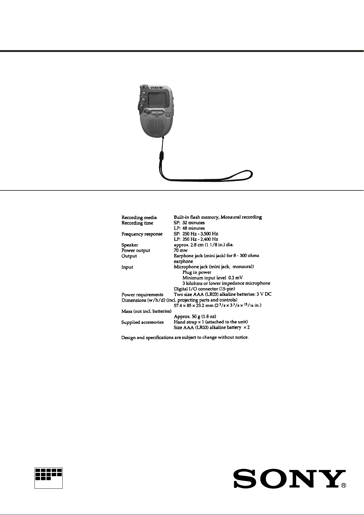
ICD-80
SERVICE MANUAL
Ver 1.0 1998. 07
SPECIFICATIONS
US Model
MICROFILM
IC RECORDER
Page 2

SECTION 1
SERVICING NOTES
TABLE OF CONTENTS
1. SERVICING NOTES............................................... 2
2. GENERAL ................................................................... 3
3. DISASSEMBLY ......................................................... 4
4. DIAGRAMS
4-1. Block Diagram ................................................................ 5
4-2. Schematic Diagram ......................................................... 8
4-3. Printed Wiring Board ...................................................... 11
4-4. IC Pin Function Description ........................................... 16
5. EXPLODED VIEW................................................... 19
6. ELECTRICAL PARTS LIST ............................... 20
CAUTION ON REPLACING FLASH MEMORY
The BAD-BLOCK check* must be executed, when the flash
memory in this set was replaced.
The set will not operate normally, unless this check is finished.
* T he BAD-BLOCK check detects an area (bad-block) in the flash
memory where data validity cannot be guaranteed, and saves
this information in the TOC-AREA so that a bad-block is not
used.
BAD-BLOCK Check Procedure:
1. Apply 3.0 V from re gulated power supply to the battery terminals.
(The battery lid open/close detection switch S701 may be kept
off)
2. Red LED and green LED light up.
3. As “Push St & Er” is displayed on the LCD, press the STOP
(S703) button and the ERASE (S702) button simultaneously.
(BAD-BLOCK check will start)
4. “Bad Check” is displayed on the LCD. (Check will last for
about 90 sec, and keep applying regulated power supply during checking)
5. Backlight turns on (B AD-BLOCK check finished successfully)
(*)
Red and green LEDs turn off. “Good OK!” is displayed on
the LCD.
(*): In case of NG, “Bad Memory” is displayed on the LCD.
6. Press the RESET (S501) button.
Note:
• In case of NG, check the System Control IC, Memory IC, and
their peripheral circuits. (Particularly, check carefully the soldering of the flash memory)
• After finishing the BAD-BLOCK check, assemble the set, load
the battery, and confirm if the set operates normally.
Flexible Circuit Board Repairing
• Keep the temperature of the soldering iron around 270 ˚C dur-
ing repairing.
• Do not touch the soldering iron on the same conductor of the
circuit board (within 3 times).
• Be careful not to apply force on the conductor when soldering
or unsoldering.
Notes on chip component replacement
• Never reuse a disconnected chip component.
• Notice that the minus side of a tantalum capacitor may be dam-
aged by heat.
– 2 –
Page 3
SECTION 2
GENERAL
This section is extracted from
instruction manual.
– 3 –
Page 4
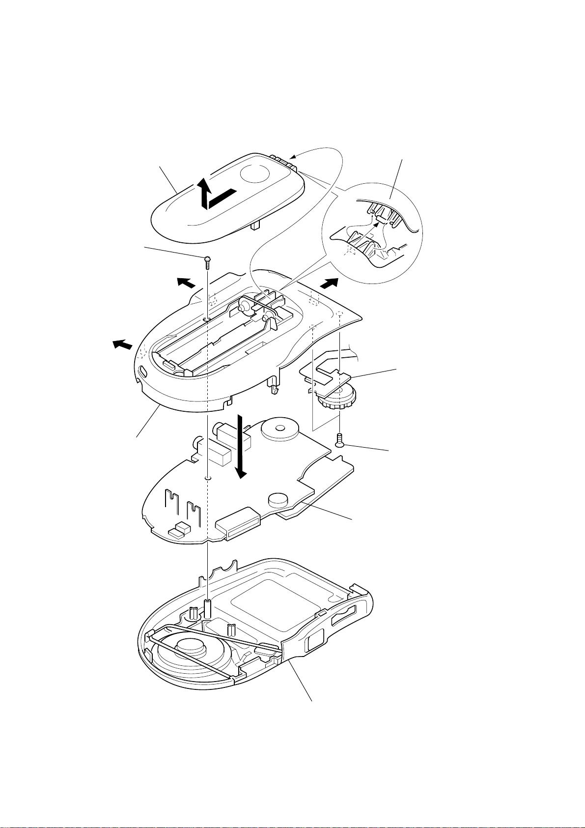
SECTION 3
d
DISASSEMBLY
Note: Follow the disassembly procedure in the numerical order given.
BATTERY CASE LID, MAIN BOARD
1
battery case lid
A
2
tapping screw
(B1.7)
Pull the battery case lid towar
direction A, remove it.
7
case block assy
4
MAIN board
6
switch unit
5
two screws
(M1.7
×
2.5)
– 4 –
3
upper lid block assy
Page 5
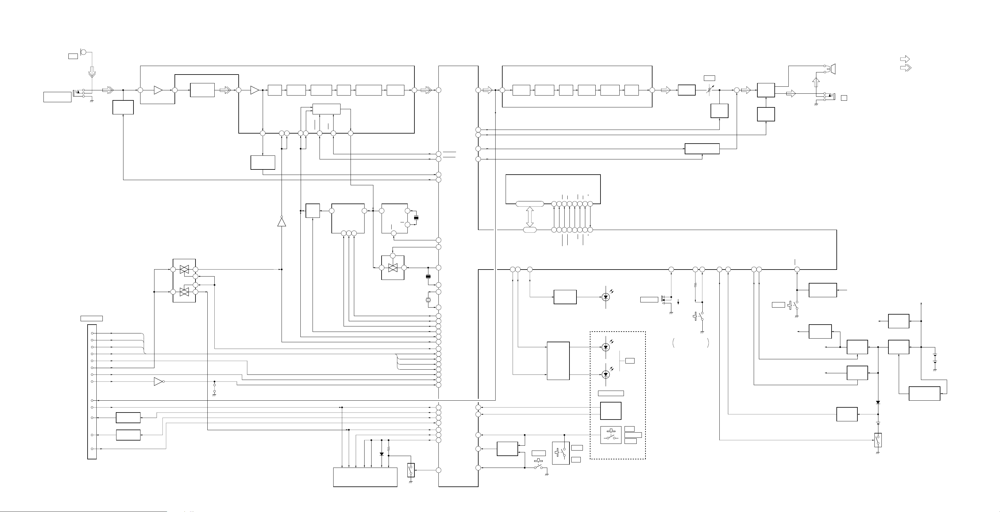
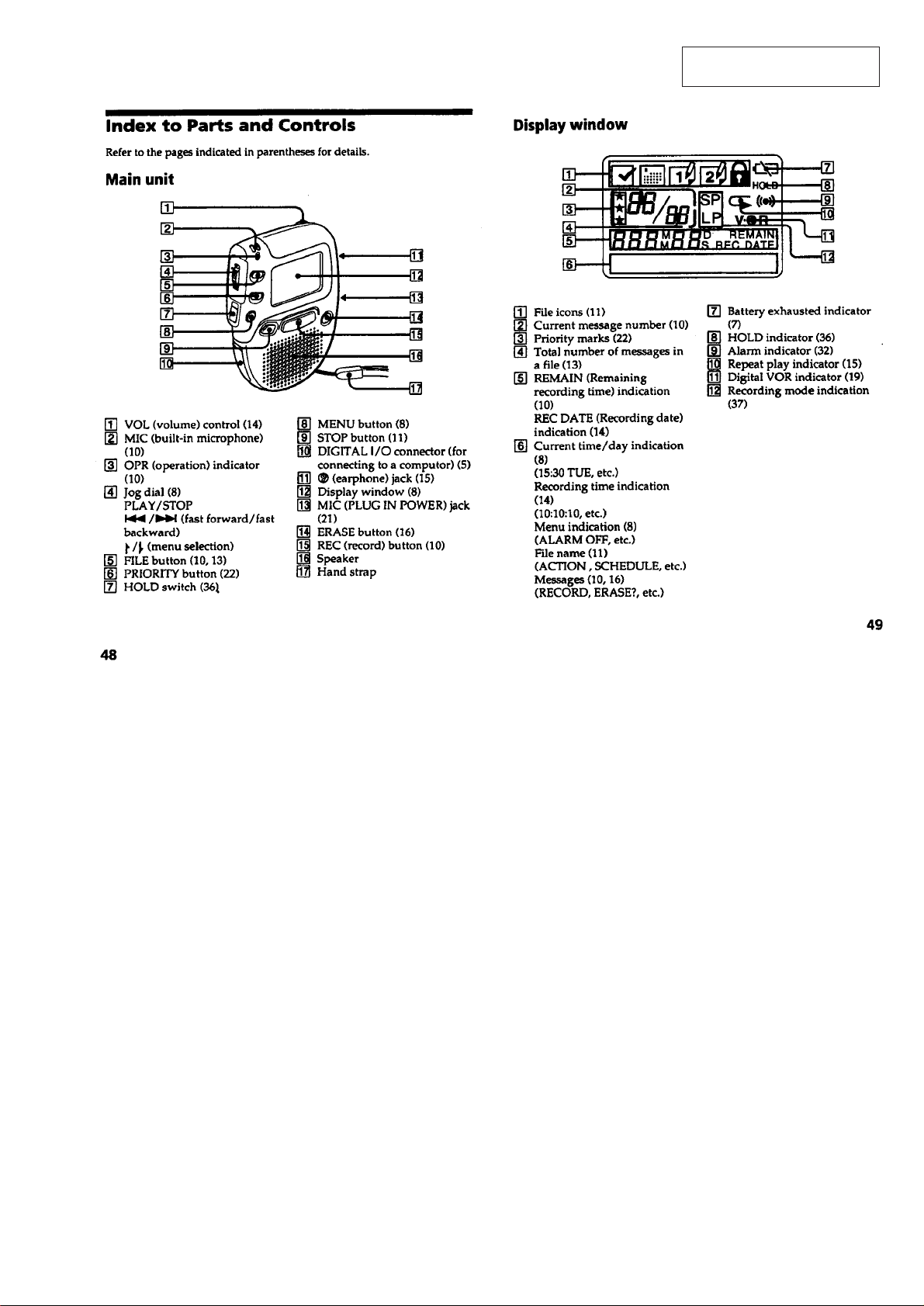
4-1. BLOCK DIAGRAM
MIC101
MIC
J101
MIC
PLUG IN POWER
MIC SENSE
SWITCH
Q103
SECTION 4
DIAGRAMS
ADPCM
IC101 (1/2)
AIN1 GSX1
12 13
AGC CIRCUIT
D101, D102,
IC103, Q104
ICD-80
• SIGNAL PATH
SYSTEM CONTROLLER
IC701
AIN2
14
L.P.F.
GSX2
15
BCLKA28BCLKB
27
A/D
CONVETER
XSYNC25RSYNC
26
DECIMETER
TIMING
GENERATOR
RESET
1
PDN
21
B.P.F.
MCK
24
COMPRESSOR
DECODER
ADPCM
IS
5
PIA IS69POA IR
68
12PO MUTE
51PO PAMP
ADPCM
IC101 (2/2)
IR
4
ADPCM
DECODER
EXPANDER
L.P.F.
INTER-
POLATOR
D/A
CONVETER
L.P.F.
VFRO
: PLAY
SP101
RV101
VOL
16
TONE
CONTROL
LINE
MUTING
Q105
+
POWER
AMP
IC105
STANDBY
SWITCH
Q106
(SPEAKER)
J102
@
(EARPHONE)
: REC
DATA0 (COM0)
DATA1 (COM1)
DATA2 (COM2)
DATA3 (COM3)
DATA4 (REQUEST)
DATA5 (SCLK)
DATA6 (C/D)
DATA7 (TEST)
STATUS4 (SDATAO)
STATUS5 (SDATAI)
STATUS6 (OPT)
STATUS7 (ACK)
GND (WAV LINK)
CN703
DIGITAL I/O
1
2
3
4
5
6
7
8
9
10
11
12
13
DATA0
DATA1
DATA2
DATA3
LEVEL SHIFT
Q704 (1/2)
LEVEL SHIFT
Q704 (2/2)
Q705
CLOCK SWITCH
IC705
6 5
1 2
– 5 –
PO BEEP
PO PMUT
PI POTA
PI POTB
KEY A/D
PI WAKE
PI ERS
53
1
FLASH MEMORY
IC702
ALE
I/O0 – I/O7
18 – 21, 24 – 27
84 – 91
PO0 – PO7
PO LIGH
POL REC
POL PLY
30
27
26
80
81
63
KEY
78
8
WAKE-UP
Q701 – 703
S702
ERASE
CLE
2
3
93
94
POR ALE
POR CLE
BACK LIGHT
LED DRIVE
Q503
LED DRIVE
Q551
WEREWP
42
95496
POR WE
SE
40
98
SE
POR RE
S703
STOP
S705
REC
5
43
99
6
WP
CE
R/B
41
7
POR CE
PIR R/B
SWITCH UNIT
= – + +
(PUSH: PLAY/STOP)
(BACK LIGHT)
(PLAY: GREEN)
(REC: RED)
ROTARY
ENCODER
D503
S704
9 HOLD
OPR
FILE
PRIORITY
MENU
– 6 –
X702
6.912MHz
X703
3 POA PDN
4
POA RES
PI VOR
10
5 PO MIC
PO LPC
58
PO SPC
57
OSCO
24
OSCI
23
XO
21
XI
20
POS LE
46
44
POS DAT
45
POS CLK
PO XSDW
65
XSYNC
76
POA CLK
67
PO WLOK
33
PI COM0
39
40 PI COM1
PI COM2
41
PI COM3
42
77
PI REQ
PI C/D
50
PI TEST
48
POD DAT
72
PO OPT
32
PO ACK
31
PI WLNK
38
POD SCK
70
POD STB
71
PO LCDV
60
PO LCDR
52
VOR
DETECTOR
IC104
1
VDD
VDD2
CLOCK GENERATOR
IC704
OUT
4
2 1
D701
XT
XT
INH
1
4
CLOCK SWITCH
IC703
VREF
VLCD
REFERENCE
2
6
X701
32.768kHz
DATA0
DATA1
DATA2
DATA3
VOLTAGE
SWITCH
Q706
10.368MHz
1296 DIVIDER
DATA
LATCH
IC107
IC102
3
7
BP701
IC106
OUT
13
CLK
9
DATA
DATA
10
11
SCK
LCD MODULE
IN
CE
STB
GAIN DOWN MUTING
PI HOLD
9
OFF
ON
S701
BATTERY LID
OPEN/CLOSE DETECT
Q107
PO BOP79PI OPEN
56
PO BACK
14
PI DET3
11
PO BOT
13
PO REGU
15
S501
RESET
MIC CIRCUIT B+
RST
82
RESET SIGNAL
GENERATOR
IC502
REGULATOR
Q101, 102
+3.3V
BACK UP B+
VOLTAGE
DETECTOR
– 7 –
BACK UP B+
REGULATOR
IC503
+3.3V
IC501
B+
SWITCH
Q501
+2.1V
LED B+
D501
BT501
BACK UP
CONTROL
SWITCH
Q552
+2.1V
REGULATOR
IC551
DC/DC
CONVERTER
IC504
POWER AMP
(IC105) B+
DC/DC CONVERTER
CONTROL
IC505, Q502
DRY BATTERY
SIZE “AAA”
(IEC DESIGNATION R03)
2PCS. 3V
Page 6

• Waveforms
– MAIN Board –
1 IC701 @¡ (XO)
1 V/DIV, 10 µs/DIV
32.768 kHz
2 IC701 @¢ (OSCO)
1 V/DIV, 50 ns/DIV
2.5 Vp-p
2.8 Vp-p
10.368 MHz
3 IC704 6 (Rec LP mode)
1 V/DIV, 50 ns/DIV
6.912 MHz
4 IC504 4 (LX) (Stop)
1 V/DIV, 500 µs/DIV
4 Vp-p
3.8 Vp-p
10
µ
s
– 13 –
Page 7

• IC Block Diagrams
– MAIN Board –
IC101 MSM7560LGS-KDR1
X2X1VDDAGDG
232120
22
AIN1
GSX1
AIN2
GSX2
–
12
+
13
–
14
+
15
RC
L.P.F.
CONVERTER
A/D
910
DECIMETER
B.P.F.
O
COMPRESSOR
I
I
O
ADPCM
DECODER
S/P
XSYNC
26
IS
5
27
BCLKA
11
24
19
18
17
16
1
8
REFERENCE
VOLTAGE
TIMING
GENERATOR
-1
–
+
RC
L.P.F.
CONVERTER
SG
PDN
MCK
RES
LPS
AOUT+
AOUT–
PWI
VFRO
IC104 NJM2072M
D/A
INTER-
POLATOR
L.P.F.
O
I
I
O
ADPCM
O
EXPANDER
I
O
I
DECODER
S/P
S/P
S/P
S/P
S/P
28
25
7
6
2
3
4
PCMSO
PCMSI
BCLKB
PCMRI
PCMRO
IR
RSYNC
INPUT
GAIN CONT
AMP OUT
GND
1
2
3
4 5
VCC
8
OUTPUT2
7
OUTPUT1
6
RECOVERY
TIME CAP
– 14 –
Page 8

IC106 SM5158AM-E2
XIN
1
2
XOUT
DATA
10
CLK
9
LE
11
8
FIN
IC107 TC7W74FU
CLR
PR
VCC
8
1
CK
6
7
RSQ
QDC
3
2
Q
D
5
4
Q
GND
16 BIT R COUNTER
16 BIT LATCH
17 BIT SHIFT REGISTER
16 BIT LATCH
16 BIT N COUNTER
IC704 XC2141C21AMR
INH
XT
VSS
FR
13
LOCK
DETECTOR
PHASE
DETECTOR
1
2
3
CHARGE
PUMP
BUFFER
XT
6
VDD
5
Q0
4
LD
7
DOA
12
DOP
5
16
OR
OV
15
FV
3
– 15 –
Page 9

4-4. IC PIN FUNCTION DESCRIPTION
• MAIN BOARD IC701 MN102L25DSD (SYSTEM CONTROLLER)
Pin No. Pin Name I/O
1 PO PMUT O
2 PO LPCI O
3 POA PDN O
4 POA RES O
5 PO MIC O
6 POR CE O
7 PIR R/B I
8 PI ERS I
9 PI HOLD I
10 PI VOR I
11 PI DET3 I
12 PO MUTE O
13 PO BOT O
14 PO BACK O
15
16 PO DDC O
17 VDD —
18 SYSCLK O
19 VSS —
20 XI I
21 XO O
22 VDD —
23 OSCI I
24 OSCO O
25 MODE I
26 POL REC O
27 POL PLY O
28 — O
29 — O
30 PO LIGH O
31 PO ACK O
32 PO OPT O
33 PO WLOK O
34 VDD —
35 — O
36 — O
37 — O
38 PI WLNK I
39 PI COM0 I
40 PI COM1 I
41 PI COM2 I
42 PI COM3 I
PO REGU O
Function
Gain down muting on/off control signal output to the power amplifier (IC105) “H”: muting on
Not used (open)
Power down control signal output to the MSM7560LGS (IC101) “L”: power down
Reset signal output to the MSM7560LGS (IC101) “L”: reset
Microphone sensitivity selection signal output for the microphone input “L”: low, “H”: high
Chip enable signal output to the flash memory (IC702)
Ready/busy monitor input from the flash memory (IC702)
ERASE switch (S702) input terminal When the key pressing “L”
9 HOLD switch (S704) input terminal “L”: hold on, “H”: hold off
Detect whether audio signal is entered or not input from the VOR detection circuit (IC104)
“L”: signal is entered, “H”: no signal entered
Power supply voltage detection input of the back-up power supply
Line muting on/off control signal output terminal “H”: line muting on
Power on/off section signal output of the back-up power supply “H”: power on
Connection control signal output of the back-up power supply
Power supply voltage detection input of the +3.3V and mic circuit power supply
“H”: power on
Power on/off control signal output of the DC/DC converter “H”: power on
Not used (open)
Power supply terminal (+3.4V)
Not used (open)
Ground terminal
Sub system clock input terminal (32.768 kHz)
Sub system clock output terminal (32.768 kHz)
Power supply terminal (+3.4V)
Main system clock input terminal (10.368 MHz)
Main system clock output terminal (10.368 MHz)
Setting terminal for the CPU operational mode (fixed at “H” in this set)
LED drive signal output of the OPR REC indicator (red) “H”: LED on (recording mode)
LED drive signal output of the OPR PLAY indicator (green) “H”: LED on (play mode)
Not used (open)
Not used (open)
LED drive signal output of the LCD back light “H”: LED on
Acknowledge signal output to the equipment connected to digital I/O connector (CN703)
OPT control signal output to the equipment connected to digital I/O connector (CN703)
Output of enable control signal when loading serial data from the equipment connected to digital I/O
connector (CN703) “H” active
Power supply terminal (+3.4V)
Not used (open)
Not used (open)
Not used (open)
For detecting the connection of the equipment connected to digital I/O connector (CN703)
“L”: connection (link), “H”: no connection
Link data (0) input from the equipment connected to digital I/O connector (CN703)
Link data (1) input from the equipment connected to digital I/O connector (CN703)
Link data (2) input from the equipment connected to digital I/O connector (CN703)
Link data (3) input from the equipment connected to digital I/O connector (CN703)
– 16 –
Page 10

Pin No. Pin Name I/O
43 VSS —
44 POS DAT O
45 POS CLK O
46 POS LE O
47 PI CHK0 I
48 PI TEST I
49 PI TCLK I
Function
Ground terminal
Serial data output to the 1296 divider (IC106)
Serial data transfer clock signal output to the 1296 divider (IC106)
Serial data latch pulse output to the 1296 divider (IC106)
Not used (fixed at “L”)
Setting terminal for the test mode “L”: test mode
Not used (open)
50 PI C/D I
51 PO PAMP O
52 PO LCDR O
53 PO BEEP O
54 VDD —
55 PO CHK1 O
56 PO BOP O
57 PO SPC O
58 PO LPC O
59 PO KEYV O
60 PO LCDV O
61 VSS —
62 BATT A/D I
63 KEY A/D I
64 — O
65 PO XSDW O
66 VDD (VPP) —
67 POA CLK O
68 PIA IS I
69 POA IR O
70 POD SCK O
71 POD STB O
72 POD DAT O
73 PULL UP I
74 PULL UP I
75 NMI I
76 XSYNC I
Command/data judging signal input from the equipment connected to digital I/O connector (CN703)
Standby on/off control signal output to the power amplifier (IC105) “L”: standby
LCD drive reference voltage control signal output to the LCD module
Beep sound drive signal output terminal
Power supply terminal (+3.4V)
Not used (open)
Battery lid open/close detection control signal output terminal
“L”: detection disabled, “H”: detection enabled
Master clock switching signal output in recording mode (LP/SP) (SP mode: 10.368 MHz)
In SP mode, “H” is output to the clock switch (IC703) to switch over the clock
Master clock switching signal output in recording mode (LP/SP) (LP mode: 6.912 MHz)
In LP mode, “L” is output to the clock generator (IC704) to switch over the clock
Key power control signal output terminal
LCD drive power control signal output to the LCD module
Ground terminal
Dry battery voltage detection signal input terminal (A/D input)
Key input terminal (A/D input) S703, 705 (STOP, REC), switch unit (FILE, PRIORITY, MENU)
keys input
Not used (open)
Clear control signal output to the data latch (IC107)
Power supply terminal (+3.4V)
Serial clock signal output to the MSM7560LGS (IC101) (Clock signal is output during serial data
transfer)
Recording serial data input from the MSM7560LGS (IC101)
Playback serial data output to the MSM7560LGS (IC101)
Serial data transfer clock signal output to the LCD module
Strobe signal output to the LCD module
Serial data output to the LCD module
Not used (fixed at “H”)
Not used (fixed at “H”)
Non-maskable interrupt input terminal
Input of signal detecting that serial transfer to the MSM7560LGS (IC101) started
77 PI REQ I
78 PI WAKE I
79 PI OPEN I
80 PI POTA I
81 PI POTB I
82 RST I
83 VDD —
Communication request signal input from the equipment connected to digital I/O connector (CN703)
Key interruption processing start signal input terminal
Battery lid open/close detection switch (S701) input terminal “L”: battery lid is closed
Rotary encoder dial pulse input of the jog dial (= – + +)
Rotary encoder dial pulse input of the jog dial (= – + +)
System reset signal input from the reset signal generator (IC502) “L”: reset
For several hundreds msec. after the power supply rises, “L” is input, then it changes to “H”
Power supply terminal (+3.4V)
– 17 –
Page 11

Pin No. Pin Name I/O
84 PO0 I/O
85 PO1 I/O
86 PO2 I/O
87 PO3 I/O
88 PO4 I/O
89 PO5 I/O
90 PO6 I/O
91 PO7 I/O
92 VSS —
93 POR CLE O
94 POR ALE O
95 POR WE O
96 POR RE O
97 — O
98 SE O
99 WP O
100 P17 O
Function
Two-way data bus with the flash memory (IC702)
Ground terminal
CLE control signal output to the flash memory (IC702)
ALE control signal output to the flash memory (IC702)
Write enable signal output to the flash memory (IC702)
Read enable signal output to the flash memory (IC702)
Not used (open)
SE control signal output to the flash memory (IC702)
WP control signal output to the flash memory (IC702)
Not used (open)
– 18 –
Page 12

SECTION 5
EXPLODED VIEW
NOTE:
• -XX and -X mean standardized parts, so they
may have some difference from the original
one.
• Color Indication of Appearance Parts
Example:
KNOB, BALANCE (WHITE) . . . (RED)
↑↑
Parts Color Cabinet's Color
21
3
• Items marked “*” are not stocked since they
are seldom required for routine service. Some
delay should be anticipated when ordering
these items.
• The mechanical parts with no reference number in the exploded views are not supplied.
• Accessories and packing materials are given
in the last of the electrical parts list.
20
SP101
15
2
ND701
6
D503
19
17
W502
4
1
W501
Ref. No. Part No. Description Remark
1 A-3293-987-A MAIN BOARD, COMPLETE
2 4-995-845-01 SPRING (SPEAKER)
3 X-4950-256-1 LID ASSY, UPPER
4 4-997-709-01 SHEET (P)
5 4-995-841-11 CAP (PC)
7
MIC101
5
9
8
10
12
11
Ref. No. Part No. Description Remark
15 4-998-440-01 SPACER (WINDOW)
17 4-998-824-01 SHEET (W)
19 4-998-748-01 SPRING (A)
20 3-951-345-01 CUSHION, PANEL
21 4-212-078-01 CUSHION (FPM)
6 3-375-114-21 SCREW (M1.7X2.5)
7 1-475-434-11 SWITCH UNIT (WITH JOG DIAL)
8 4-995-839-31 CASE
9 3-318-203-95 SCREW (B1.7), TAPPING
10 4-995-842-01 TERMINAL (+. –), BATTERY
11 4-995-840-11 LID, BATTERY CASE
12 4-212-287-01 STRAP, HAND
D503 1-517-711-11 LIGHT, LED BACK
MIC101 1-542-334-11 MICROPHONE, ELECTRET CONDENSER (MIC)
ND701 1-801-928-11 INDICATOR MODULE
SP101 1-505-854-11 SPEAKER (2.8cm)
W501 4-995-843-01 TERMINAL (+), BATTERY
W502 4-995-844-01 TERMINAL (–), BATTERY
– 19 –
Page 13

MAIN
SECTION 6
ELECTRICAL PARTS LIST
NOTE:
• Due to standardization, replacements in the
parts list may be different from the parts specified in the diagrams or the components used
on the set.
• -XX and -X mean standardized parts, so they
may have some difference from the original
one.
• RESISTORS
All resistors are in ohms.
METAL: Metal-film resistor.
METAL OXIDE: Metal oxide-film resistor.
F: nonflammable
Ref. No. Part No. Description Remark Ref. No. Part No. Description Remark
A-3293-987-A MAIN BOARD, COMPLETE
*********************
4-997-709-01 SHEET (P)
4-998-748-01 SPRING (A)
4-998-824-01 SHEET (W)
< BATTERY >
BT501 1-528-834-11 BATTERY, POLYACENE SECONDARY
< CAPACITOR >
C101 1-104-847-11 TANTALUM CHIP 22uF 20% 4V
C102 1-115-156-11 CERAMIC CHIP 1uF 10V
C103 1-162-964-11 CERAMIC CHIP 0.001uF 10% 50V
C104 1-163-077-00 CERAMIC CHIP 0.1uF 10% 25V
C105 1-164-360-11 CERAMIC CHIP 0.1uF 16V
C106 1-164-360-11 CERAMIC CHIP 0.1uF 16V
C107 1-135-149-21 TANTALUM CHIP 2.2uF 20% 10V
C108 1-164-360-11 CERAMIC CHIP 0.1uF 16V
C109 1-164-360-11 CERAMIC CHIP 0.1uF 16V
C110 1-104-847-11 TANTALUM CHIP 22uF 20% 4V
C111 1-164-360-11 CERAMIC CHIP 0.1uF 16V
C112 1-113-619-11 CERAMIC CHIP 0.47uF 10V
C113 1-164-360-11 CERAMIC CHIP 0.1uF 16V
C114 1-162-964-11 CERAMIC CHIP 0.001uF 10% 50V
C115 1-162-964-11 CERAMIC CHIP 0.001uF 10% 50V
C116 1-104-847-11 TANTALUM CHIP 22uF 20% 4V
C117 1-164-360-11 CERAMIC CHIP 0.1uF 16V
C118 1-164-360-11 CERAMIC CHIP 0.1uF 16V
C119 1-164-360-11 CERAMIC CHIP 0.1uF 16V
C120 1-162-964-11 CERAMIC CHIP 0.001uF 10% 50V
• Items marked “*” are not stocked since they
are seldom required for routine service.
Some delay should be anticipated when ordering these items.
• SEMICONDUCTORS
In each case, u: µ, for example:
uA. . : µA. . uPA. . : µPA. .
uPB. . : µPB. . uPC. . : µPC. .
uPD. . : µPD. .
• CAPACITORS
uF: µF
• COILS
uH: µH
C136 1-164-360-11 CERAMIC CHIP 0.1uF 16V
C138 1-162-970-11 CERAMIC CHIP 0.01uF 10% 25V
C139 1-162-970-11 CERAMIC CHIP 0.01uF 10% 25V
C140 1-162-970-11 CERAMIC CHIP 0.01uF 10% 25V
C141 1-162-970-11 CERAMIC CHIP 0.01uF 10% 25V
C502 1-110-569-11 TANTALUM CHIP 47uF 20% 6.3V
C503 1-162-974-11 CERAMIC CHIP 0.01uF 50V
C504 1-162-974-11 CERAMIC CHIP 0.01uF 50V
C505 1-162-974-11 CERAMIC CHIP 0.01uF 50V
C506 1-113-996-11 TANTALUM CHIP 220uF 20% 4V
C508 1-110-569-11 TANTALUM CHIP 47uF 20% 6.3V
C509 1-110-569-11 TANTALUM CHIP 47uF 20% 6.3V
C510 1-117-379-21 CERAMIC CHIP 10uF 10V
C511 1-164-360-11 CERAMIC CHIP 0.1uF 16V
C513 1-164-505-11 CERAMIC CHIP 2.2uF 16V
C701 1-162-944-11 CERAMIC CHIP 18PF 5% 50V
C702 1-162-944-11 CERAMIC CHIP 18PF 5% 50V
C703 1-164-360-11 CERAMIC CHIP 0.1uF 16V
C704 1-164-360-11 CERAMIC CHIP 0.1uF 16V
C705 1-162-974-11 CERAMIC CHIP 0.01uF 50V
C707 1-107-826-11 CERAMIC CHIP 0.1uF 10% 16V
C709 1-164-360-11 CERAMIC CHIP 0.1uF 16V
C710 1-107-826-11 CERAMIC CHIP 0.1uF 10% 16V
C711 1-164-360-11 CERAMIC CHIP 0.1uF 16V
C712 1-162-964-11 CERAMIC CHIP 0.001uF 10% 50V
C713 1-162-964-11 CERAMIC CHIP 0.001uF 10% 50V
C714 1-164-360-11 CERAMIC CHIP 0.1uF 16V
C715 1-164-360-11 CERAMIC CHIP 0.1uF 16V
< CONPOSITION CIRCUIT BLOCK >
When indicating parts by reference
number, please include the board.
C121 1-135-181-21 TANTALUM CHIP 4.7uF 20% 6.3V
C122 1-162-964-11 CERAMIC CHIP 0.001uF 10% 50V
C123 1-164-373-11 CERAMIC CHIP 0.033uF 25V
C124 1-164-360-11 CERAMIC CHIP 0.1uF 16V
C125 1-162-974-11 CERAMIC CHIP 0.01uF 50V
C127 1-135-145-11 TANTALUM CHIP 0.47uF 10% 35V
C128 1-162-964-11 CERAMIC CHIP 0.001uF 10% 50V
C129 1-117-379-21 CERAMIC CHIP 10uF 10V
C130 1-162-974-11 CERAMIC CHIP 0.01uF 50V
C131 1-104-847-11 TANTALUM CHIP 22uF 20% 4V
C133 1-164-360-11 CERAMIC CHIP 0.1uF 16V
C134 1-164-360-11 CERAMIC CHIP 0.1uF 16V
C135 1-104-847-11 TANTALUM CHIP 22uF 20% 4V
CB701 1-125-769-11 CERAMIC CHIP 0.1uF 50V
< CONNECTOR >
* CN701 1-779-997-21 CONNECTOR, FPC (ZIF) 11P
CN702 1-779-996-21 CONNECTOR, FPC (ZIF) 17P
CN703 1-779-995-11 CONNECTOR, V RINK (DIGITAL I/O)
< DIODE >
D101 8-719-059-52 DIODE MA143-TX
D102 8-719-059-52 DIODE MA143-TX
D501 8-719-049-09 DIODE 1SS367-T3SONY
D502 8-719-067-42 DIODE MA2H735-(TX).SO
– 20 –
Page 14

MAIN
Ref. No. Part No. Description Remark
D701 8-719-421-27 DIODE MA728
< FERRITE BEAD >
FB101 1-414-235-11 INDUCTOR CHIP 0uH
FB102 1-414-235-11 INDUCTOR CHIP 0uH
FB103 1-414-235-11 INDUCTOR CHIP 0uH
FB104 1-414-235-11 INDUCTOR CHIP 0uH
FB105 1-414-235-11 INDUCTOR CHIP 0uH
FB106 1-414-235-11 INDUCTOR CHIP 0uH
FB107 1-414-921-11 INDUCTOR CHIP 0uH
FB501 1-414-921-11 INDUCTOR CHIP 0uH
FB502 1-414-921-11 INDUCTOR CHIP 0uH
FB701 1-414-595-11 INDUCTOR CHIP 0uH
< IC >
IC101 8-759-487-81 IC MSM7560LGS-KDR1
IC102 8-759-031-84 IC SC7S04F
IC103 8-759-358-47 IC NJM2115V (TE2)
IC104 8-759-701-51 IC NJM2072M
IC105 8-759-347-33 IC NJM2113V-TE2
IC106 8-759-486-46 IC SM5158AM-E2
IC107 8-759-083-94 IC TC7W74FU
IC501 8-759-486-55 IC NJM2370U33-TE2
IC502 8-759-562-65 IC XC61AN2802MR
IC503 8-759-562-66 IC XC61AN3102MR
IC504 8-759-486-48 IC XC6372C351PR
IC505 8-759-545-54 IC XC61AN1702MR
IC551 8-759-497-27 IC XC62AP2102MR
IC701 8-759-544-06 IC MN102L25DSD
IC702 8-759-496-86 IC KM29V64000T-T
IC703 8-759-082-60 IC TC7S66FU
IC704 8-759-486-57 IC XC2141C21AMR
IC705 8-759-488-29 IC TC7W66FU (TE12L)
Ref. No. Part No. Description Remark
Q701 8-729-037-74 TRANSISTOR UN9213J-(TX).SO
Q702 8-729-420-24 TRANSISTOR 2SB1218A-QRS
Q703 8-729-037-63 TRANSISTOR UN9115J-(TX).SO
Q704 8-729-426-25 TRANSISTOR XP1212
Q705 8-729-037-72 TRANSISTOR UN9211J-(TX).SO
Q706 8-729-037-72 TRANSISTOR UN9211J-(TX).SO
< RESISTOR >
R101 1-216-829-11 METAL CHIP 4.7K 5% 1/16W
R102 1-216-829-11 METAL CHIP 4.7K 5% 1/16W
R103 1-216-815-11 METAL CHIP 330 5% 1/16W
R104 1-216-839-11 METAL CHIP 33K 5% 1/16W
R105 1-216-833-11 METAL CHIP 10K 5% 1/16W
R106 1-216-829-11 METAL CHIP 4.7K 5% 1/16W
R107 1-216-821-11 METAL CHIP 1K 5% 1/16W
R108 1-216-821-11 METAL CHIP 1K 5% 1/16W
R109 1-216-833-11 METAL CHIP 10K 5% 1/16W
R110 1-216-844-11 METAL CHIP 82K 5% 1/16W
R111 1-216-833-11 METAL CHIP 10K 5% 1/16W
R112 1-216-833-11 METAL CHIP 10K 5% 1/16W
R113 1-216-837-11 METAL CHIP 22K 5% 1/16W
R114 1-216-845-11 METAL CHIP 100K 5% 1/16W
R115 1-216-833-11 METAL CHIP 10K 5% 1/16W
R116 1-216-853-11 METAL CHIP 470K 5% 1/16W
R117 1-216-824-11 METAL CHIP 1.8K 5% 1/16W
R118 1-216-805-11 METAL CHIP 47 5% 1/16W
R119 1-216-825-11 METAL CHIP 2.2K 5% 1/16W
R120 1-216-837-11 METAL CHIP 22K 5% 1/16W
R121 1-216-837-11 METAL CHIP 22K 5% 1/16W
R122 1-216-841-11 METAL CHIP 47K 5% 1/16W
R123 1-216-821-11 METAL CHIP 1K 5% 1/16W
R124 1-216-833-11 METAL CHIP 10K 5% 1/16W
R125 1-216-833-11 METAL CHIP 10K 5% 1/16W
< JACK >
J101 1-568-027-11 JACK, SMALL TYPE (@ (EARPHONE))
J102 1-568-027-11 JACK, SMALL TYPE (MIC, PLUG IN POWER)
< COIL >
L503 1-414-865-11 INDUCTOR 47uH
< MICROPHONE >
MIC101 1-542-334-11 MICROPHONE, ELECTRET CONDENSER (MIC)
< TRANSISTOR >
Q101 8-729-429-44 TRANSISTOR XP1501
Q102 8-729-037-63 TRANSISTOR UN9115J-(TX).SO
Q103 8-729-037-72 TRANSISTOR UN9211J-(TX).SO
Q104 8-729-120-28 TRANSISTOR 2SC1623-L5L6
Q105 8-729-039-57 TRANSISTOR DTC363EKT146
Q106 8-729-037-72 TRANSISTOR UN9211J-(TX).SO
Q107 8-729-037-76 TRANSISTOR UN9215J-(TX).SO
Q501 8-729-402-16 TRANSISTOR XN4608
Q502 8-729-046-70 TRANSISTOR XP4654-(TX).SO
Q503 8-729-230-63 TRANSISTOR 2SC4116-YG
Q551 8-729-426-25 TRANSISTOR XP1212
Q552 8-729-028-28 FET 2SK2036(TE85L)
R126 1-216-833-11 METAL CHIP 10K 5% 1/16W
R127 1-216-845-11 METAL CHIP 100K 5% 1/16W
R128 1-216-817-11 METAL CHIP 470 5% 1/16W
R129 1-216-833-11 METAL CHIP 10K 5% 1/16W
R130 1-216-827-11 METAL CHIP 3.3K 5% 1/16W
R131 1-218-296-11 RES,CHIP 75K 5% 1/16W
R132 1-216-799-11 METAL CHIP 15 5% 1/16W
R134 1-216-825-11 METAL CHIP 2.2K 5% 1/16W
R135 1-216-821-11 METAL CHIP 1K 5% 1/16W
R136 1-216-821-11 METAL CHIP 1K 5% 1/16W
R137 1-216-824-11 METAL CHIP 1.8K 5% 1/16W
R138 1-216-824-11 METAL CHIP 1.8K 5% 1/16W
R139 1-216-824-11 METAL CHIP 1.8K 5% 1/16W
R140 1-216-824-11 METAL CHIP 1.8K 5% 1/16W
R141 1-216-824-11 METAL CHIP 1.8K 5% 1/16W
R501 1-216-845-11 METAL CHIP 100K 5% 1/16W
R502 1-216-853-11 METAL CHIP 470K 5% 1/16W
R503 1-216-845-11 METAL CHIP 100K 5% 1/16W
R504 1-216-845-11 METAL CHIP 100K 5% 1/16W
R505 1-216-833-11 METAL CHIP 10K 5% 1/16W
R506 1-216-821-11 METAL CHIP 1K 5% 1/16W
R507 1-216-789-11 METAL CHIP 2.2 5% 1/16W
R508 1-216-809-11 METAL CHIP 100 5% 1/16W
R509 1-216-841-11 METAL CHIP 47K 5% 1/16W
R510 1-216-845-11 METAL CHIP 100K 5% 1/16W
– 21 –
Page 15

ICD-80
MAIN
Ref. No. Part No. Description Remark
R511 1-216-821-11 METAL CHIP 1K 5% 1/16W
R512 1-216-833-11 METAL CHIP 10K 5% 1/16W
R513 1-216-845-11 METAL CHIP 100K 5% 1/16W
R514 1-216-853-11 METAL CHIP 470K 5% 1/16W
R515 1-216-853-11 METAL CHIP 470K 5% 1/16W
R516 1-216-849-11 METAL CHIP 220K 5% 1/16W
R517 1-216-845-11 METAL CHIP 100K 5% 1/16W
R701 1-216-850-11 METAL CHIP 270K 5% 1/16W
R703 1-216-839-11 METAL CHIP 33K 5% 1/16W
R704 1-216-839-11 METAL CHIP 33K 5% 1/16W
R705 1-216-850-11 METAL CHIP 270K 5% 1/16W
R708 1-216-855-11 METAL CHIP 680K 5% 1/16W
R709 1-216-845-11 METAL CHIP 100K 5% 1/16W
R710 1-216-809-11 METAL CHIP 100 5% 1/16W
R711 1-216-821-11 METAL CHIP 1K 5% 1/16W
R712 1-216-857-11 METAL CHIP 1M 5% 1/16W
R713 1-216-854-11 METAL CHIP 560K 5% 1/16W
R714 1-216-853-11 METAL CHIP 470K 5% 1/16W
R715 1-218-885-11 RES,CHIP 39K 0.5% 1/16W
R716 1-218-911-11 RES,CHIP 470K 0.5% 1/16W
R717 1-216-855-11 METAL CHIP 680K 5% 1/16W
R718 1-216-855-11 METAL CHIP 680K 5% 1/16W
R719 1-216-855-11 METAL CHIP 680K 5% 1/16W
R720 1-218-863-11 RES,CHIP 4.7K 0.5% 1/16W
R721 1-218-871-11 RES,CHIP 10K 0.5% 1/16W
R722 1-218-875-11 RES,CHIP 15K 0.5% 1/16W
R723 1-218-879-11 RES,CHIP 22K 0.5% 1/16W
R724 1-218-887-11 RES,CHIP 47K 0.5% 1/16W
R725 1-216-821-11 METAL CHIP 1K 5% 1/16W
R726 1-216-821-11 METAL CHIP 1K 5% 1/16W
R727 1-216-821-11 METAL CHIP 1K 5% 1/16W
R728 1-216-821-11 METAL CHIP 1K 5% 1/16W
R729 1-216-833-11 METAL CHIP 10K 5% 1/16W
R730 1-216-809-11 METAL CHIP 100 5% 1/16W
R731 1-216-809-11 METAL CHIP 100 5% 1/16W
Ref. No. Part No. Description Remark
< VARIABLE RESISTOR >
RV101 1-225-500-11 RES, VAR, CARBON 10K/10K (VOL)
< SWITCH >
S501 1-692-481-11 SWITCH, KEY BOARD (RESET)
S701 1-692-863-21 SWITCH, PUSH (1 KEY)
(BATTRY LID OPEN/CLOSE DETECT)
S702 1-771-274-11 SWITCH, TACTILE (ERASE)
S703 1-771-274-11 SWITCH, TACTILE (STOP)
S704 1-572-922-11 SWITCH, SLIDE (9 HOLD)
S705 1-771-274-11 SWITCH, TACTILE (REC)
< BATTERY TERMINAL >
W501 4-995-843-01 TERMINAL (+), BATTERY
W502 4-995-844-01 TERMINAL (–), BATTERY
< VIBRATOR >
X701 1-760-928-21 VIBRATOR, CRYSTAL (32.768kHz)
X702 1-767-759-11 VIBRATOR, CERAMIC (6.912MHz)
X703 1-767-683-11 VIBRATOR, CERAMIC (10.368MHz)
************************************************************
MISCELLANEOUS
***************
7 1-475-434-21 SWITCH UNIT (WITH JOG DIAL)
D503 1-517-711-11 LIGHT, LED BACK
ND701 1-801-928-11 INDICATOR MODULE
SP101 1-505-854-11 SPEAKER (2.8cm)
************************************************************
ACCESSORIES & PACKING MATERIALS
********************************
3-864-397-11 MANUAL, INSTRUCTION (ENGLISH)
R732 1-216-809-11 METAL CHIP 100 5% 1/16W
R733 1-216-809-11 METAL CHIP 100 5% 1/16W
R734 1-216-833-11 METAL CHIP 10K 5% 1/16W
R735 1-216-833-11 METAL CHIP 10K 5% 1/16W
R736 1-218-895-11 RES,CHIP 100K 0.5% 1/16W
R737 1-218-895-11 RES,CHIP 100K 0.5% 1/16W
R740 1-216-833-11 METAL CHIP 10K 5% 1/16W
R741 1-216-831-11 METAL CHIP 6.8K 5% 1/16W
R744 1-216-845-11 METAL CHIP 100K 5% 1/16W
R745 1-216-845-11 METAL CHIP 100K 5% 1/16W
R746 1-216-845-11 METAL CHIP 100K 5% 1/16W
R747 1-216-846-11 METAL CHIP 120K 5% 1/16W
R748 1-216-831-11 METAL CHIP 6.8K 5% 1/16W
R749 1-216-831-11 METAL CHIP 6.8K 5% 1/16W
R799 1-216-817-11 METAL CHIP 470 5% 1/16W
< CONPOSITION CIRCUIT BLOCK >
RB701 1-233-967-11 RES, NETWORK (CHIP TYPE) 10K
RB702 1-233-969-11 RES, NETWORK (CHIP TYPE) 22K
RB703 1-233-969-11 RES, NETWORK (CHIP TYPE) 22K
RB704 1-233-967-11 RES, NETWORK (CHIP TYPE) 10K
Sony Corporation
9-924-947-11
Personal A&V Products Company
– 22 –
Printed in Singapore © 1998. 7
98G057018-1
Published by Quarity Engineering Dept.
(Shibaura)
 Loading...