Sony ICD-55 Service manual
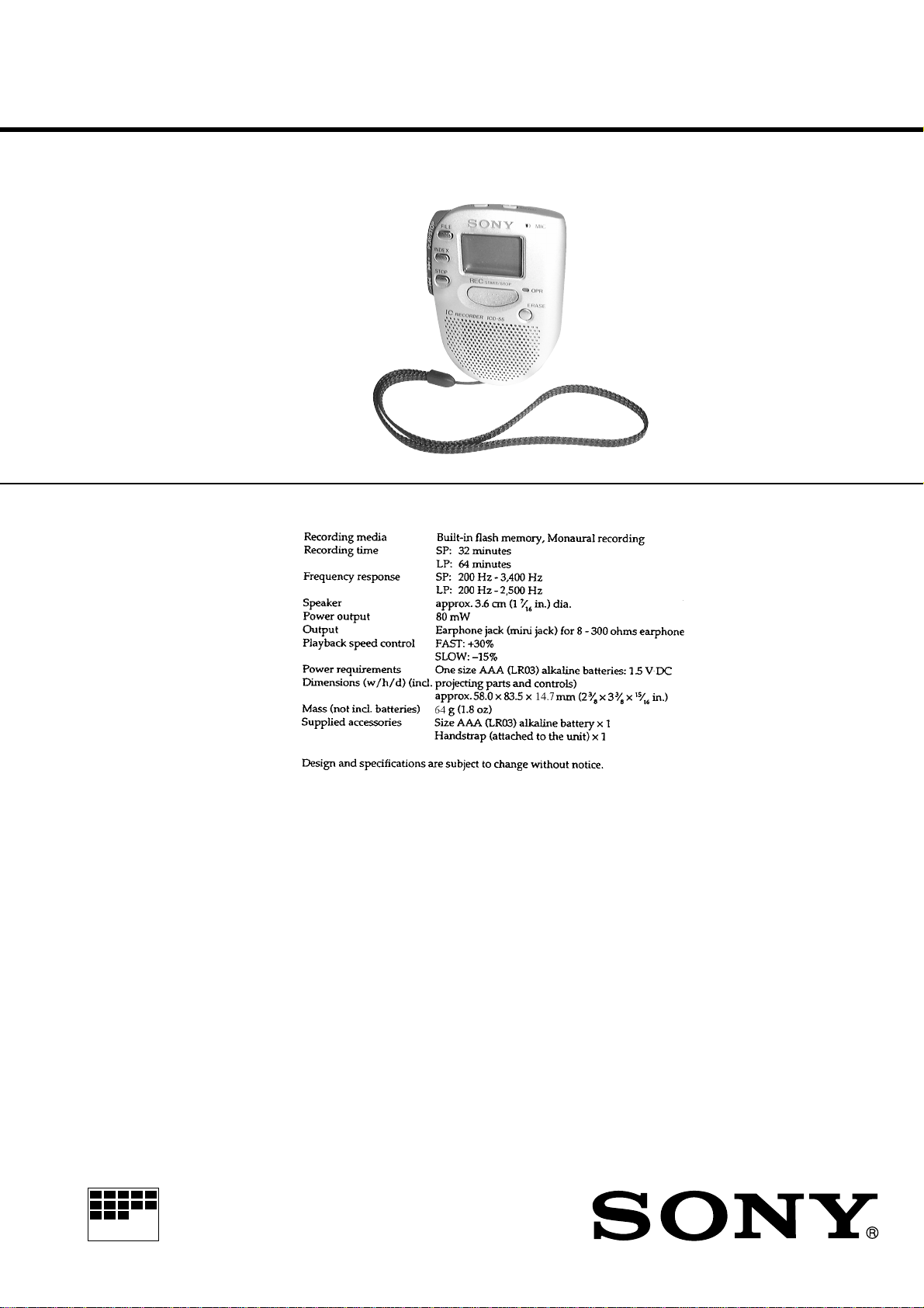
ICD-55
SERVICE MANUAL
Ver 1.2 2000. 05
With SUPPLEMENT-1
(9-926-902-83)
SPECIFICATIONS
US Model
Canadian Model
AEP Model
E Model
Tourist Model
MICROFILM
IC RECORDER

SECTION 1
SERVICING NOTES
TABLE OF CONTENTS
1. SERVICING NOTES............................................... 2
2. GENERAL ................................................................... 3
3. DISASSEMBLY ......................................................... 4
4. DIAGRAMS
4-1. Block Diagram ................................................................ 7
4-2. Printed Wiring Board ...................................................... 9
4-3. Schematic Diagram ......................................................... 11
4-4. IC Pin Function Description ........................................... 17
5. EXPLODED VIEW................................................... 19
6. ELECTRICAL PARTS LIST ............................... 20
CAUTION ON REPLACING FLASH MEMORY
The BAD-BLOCK check* must be executed, when the flash
memory in this set was replaced.
The set will not operation normally, unless this check is finished.
* The BAD-BLOCK check detects an area (bad-block) in the flash
memory where data validity cannot be guaranteed, and saves this
information in the TOC-AREA so that a bad-block is not used.
BAD-BLOCK check Procedure:
1. Apply 1.5V from re gulated po wer supply to the battery terminals.
2. Once the po wer is supplied, the check starts and then proceeds
for approx. 20 seconds. (Be sure to keep applying the power
during the check)
3. When the check completes, the result is shown as bellows.
OK:Only the LCD back light LED (D503) turns on.
NG:Red LED blinks or turns on or green LED turns on in the
OPR LED (D504).
4. In case of OK, press the
Note:
• In case of NG, check system control IC (IC701), flash memory IC and
the peripheral circuit. (Particularly , check carefully the soldering of the
flash memory)
• After finishing the BAD-BLOCK check, assemble the set, load the dry
battery, and confirm if the set operates normally.
[STOP] button.
Notes on chip component replacement
• Never reuse a disconnected chip component.
• Notice that the minus side of a tantalum capacitor may be dam-
aged by heat.
Flexible Circuit Board Repairing
• Keep the temperature of the soldering iron around 270 ˚C dur-
ing repairing.
• Do not touch the soldering iron on the same conductor of the
circuit board. (within 3 times)
• Be careful not to apply force on the conductor when soldering
or unsoldering.
– 2 –
SECTION 2
GENERAL
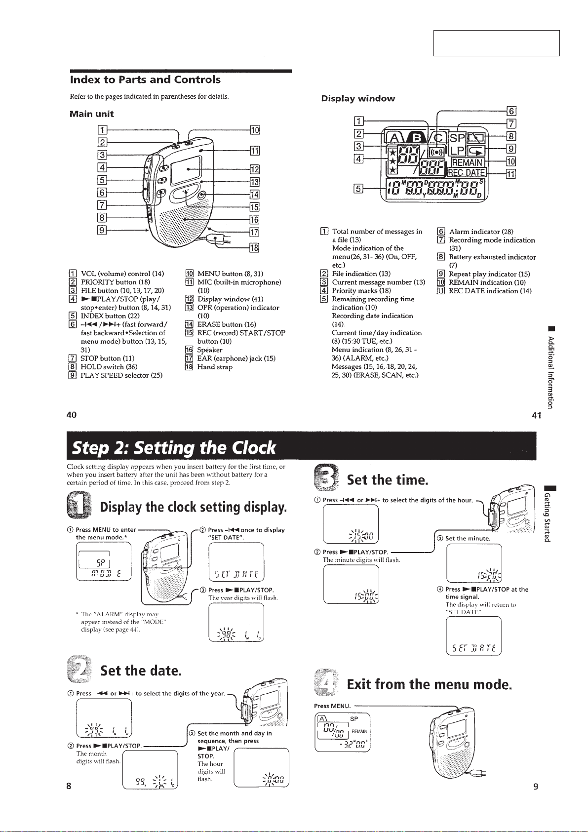
This section is extracted from
instruction manual.
– 3 –
SECTION 3
DISASSEMBLY
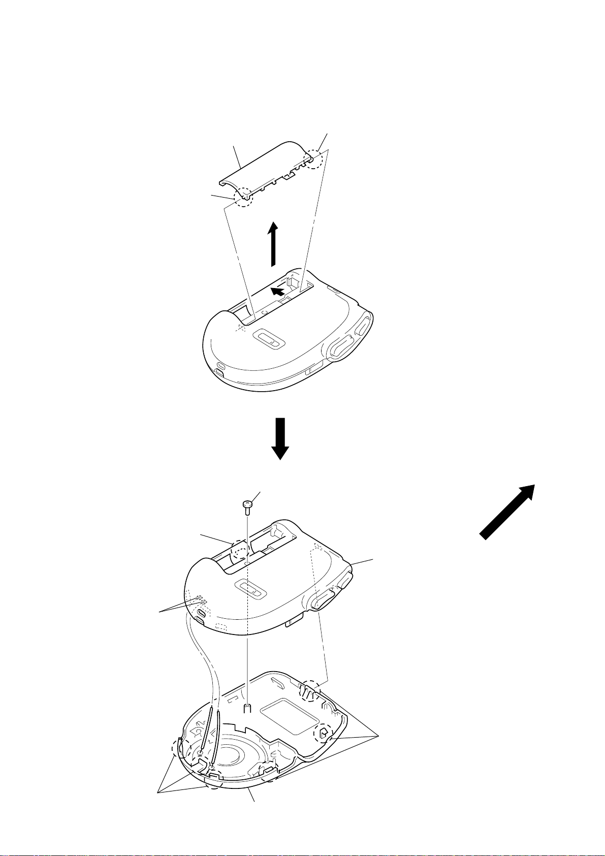
Note: Follow the disassembly procedure in the numerical order given.
LID, BATTERY CASE
3
lid, battery case
2
boss
1
2
boss
CASE (FRONT)/(REAR) SECTION
2
claw
3
Remove the two solders
speaker lead (SP101).
1
screw (1.7 × 4.5)
5
case (rear) section
2
three claws
2
three claws
4
case (front) section
– 4 –
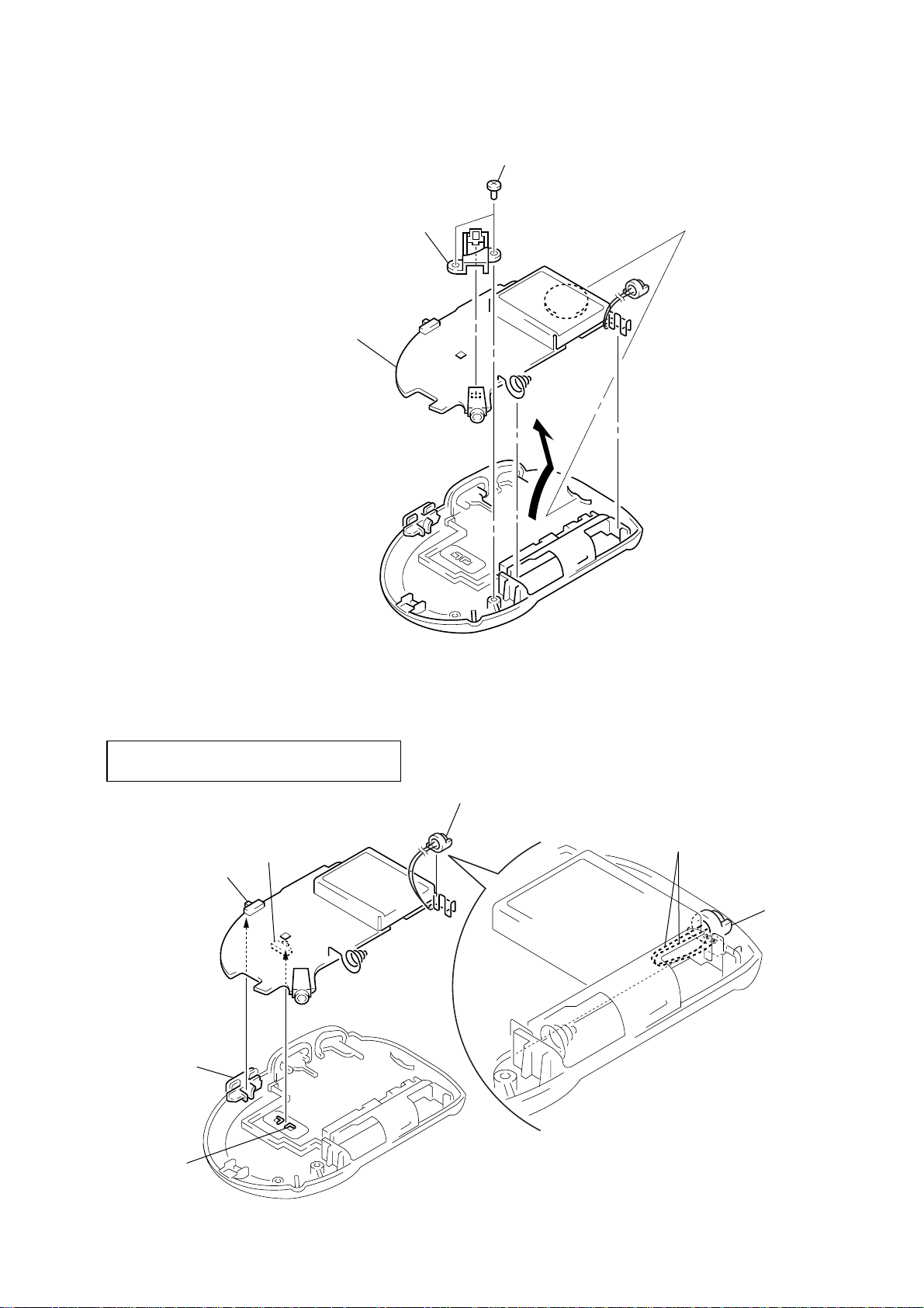
MAIN BOARD
r
3
Remove the MAIN board to
direction of the arrow.
2
bracket
(jack)
1
two screws
(M1.7
×
4)
INSTALLATION “MAIN BOARD”, “MICROPHONE, ELECTRIC CONDENSER” (MIC101)
On installation MAIN board adjust the S711, S712
and knob (HOLD, MODE).
S712
S711
knob (HOLD)
knob (MODE)
microphone, electric condenser
(MIC101)
two leads
Install two leads the electric condenser microphone
(MIC101) in the figure.
microphone,
electric condense
(MIC101)
– 5 –
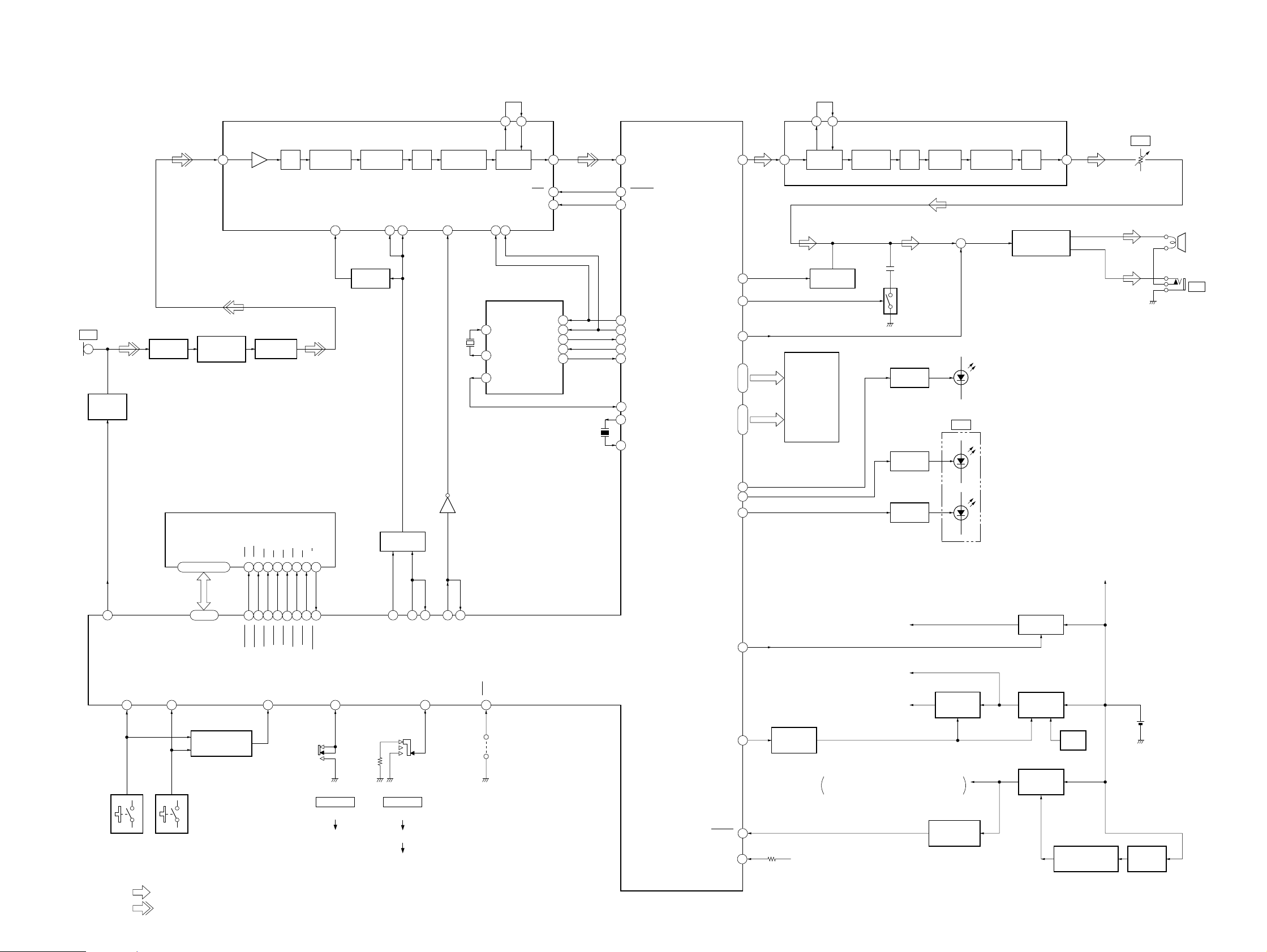
4-1. BLOCK DIAGRAM
ICD-55
SECTION 4
DIAGRAMS
MIC101
MIC
MIC SENSE
SWITCH
Q103
MIC AMP
IC103 (1/2)
AGC CIRCUIT
D101, 102,
Q104
I/O0 – I/O7
18 – 21, 24 – 27
ADPCM
IC101 (1/2)
AIN2
6
FLASH MEMORY
IC702
CLE
BUFFER
IC103 (2/2)
ALE
WEREWP
42
L.P.F.
SE
40195743
A/D
CONVERTER
MCK
22 29
CE
R/B
41
DECIMATION
FILTER
DIVIDER
IC104
RSYNC
XSYNC
30 31
GATE SWITCH
IC705
B.P.F.
COMPRESSOR
BCLK
X701
32.768kHz
IC706
28 27
PCMSO
ADPCM
ENCODER
EXCK
DIN
19 20
REAL TIME CLOCK
OSCIN
9
OSCOUT
8
32KOUT
1
PCMSI
IC703
IS
26 25 872
14
PDN
DEN
21
4
SI
2
SCLK
SO
3
7
CE
6
INTR
X702
5MHz
71
65
76
77
75
70
87
82
79
80
DSPIS
XPDRST
XDSPDEN
RTCDO
RTCCLK
RTCDI
RTCCE
RTCINT
XT1
X2
X1
SYSTEM CONTROLLER
IC701
DSPIR
LMUTE
LPMODE
BEEP
LIGHT
LEDPB
LEDREC
73
5
89
21
32 – 61
S0 – S29
23 – 26
COM0 – COM3
22
67
66
24 23
PCMRO
IR
ADPCM
DECODER
LINE MUTING
Q105
ND701
LIQUID CRYSTAL
DISPLAY
IC101 (2/2)
PCMRI
EXPANDER
TONE CONTROL
SWITCH
Q150
ADPCM
INTER-
L.P.F. L.P.F.
POLATOR
D/A
CONVERTER
+
LED DRIVE
Q505
LED DRIVE
Q506 (1/2)
LED DRIVE
Q506 (2/2)
D504
OPR
D503
(LCD BACK LIGHT)
(PLAY)
GRN
(REC)
RED
VFRO
POWER AMP
IC102, Q108, 109
BATT B+
RV101
VOL
SP101
(SPEAKER)
J101
EAR
6
MICSEL
KEY0
1
S701 – S705 S706 – S710
• SIGNAL PATH
: PLAY
05
: REC
FMIO0 – FMIO7
KEY1
2
91 – 98
WAKE UP CONTROL
SWITCH
Q701 – 703
14211310417
XFMWE
XFMALE
XFMCLE
WAKEUP
86
20
XFMSE
XFMRE
XFMCE
XFMWP
13
XFMBSY
C HOLD
HOLD
S711
OFF
XHOLD
4
15
16
SYNCMSK
S712
PLAY SPEED
FAST
NORMAL
SLOW
85
SYNCIN
SYNCOUT
SPDSW
3
74
XBCK
MSKCLK
1.5V
(POWER AMP (IC102) B+)
68
AMPPO
3.5V
(LED B+)
TEST
64
TP701
(TEST)
XSPOWER
XRESET
BATT
69
84
100
POWER
SWITCHING
Q508
BATT B+
MEMORY (IC702), REAL TIME CLOCK (IC703) B+
3.3V
(ADPCM (IC101) B+)
SYSTEM CONTROLLER (IC701), FLASH
3.3V
18
– 7 – – 8 –
+3.3V
REGULATOR
IC503
RESET SIGNAL
GENERATOR
IC505
B+ SWITCH
Q106, 107
DC/DC
CONVERTER
IC502
DC/DC
CONVERTER
IC501
OSC
Q502
DC/DC CONVERTER
CONTROL
Q507
DRY BATTERY
SIZE “AAA”
(IEC DESIGNATION R03)
1P. 1.5V
VOLTAGE
DETECT
IC504
 Loading...