

Page 1
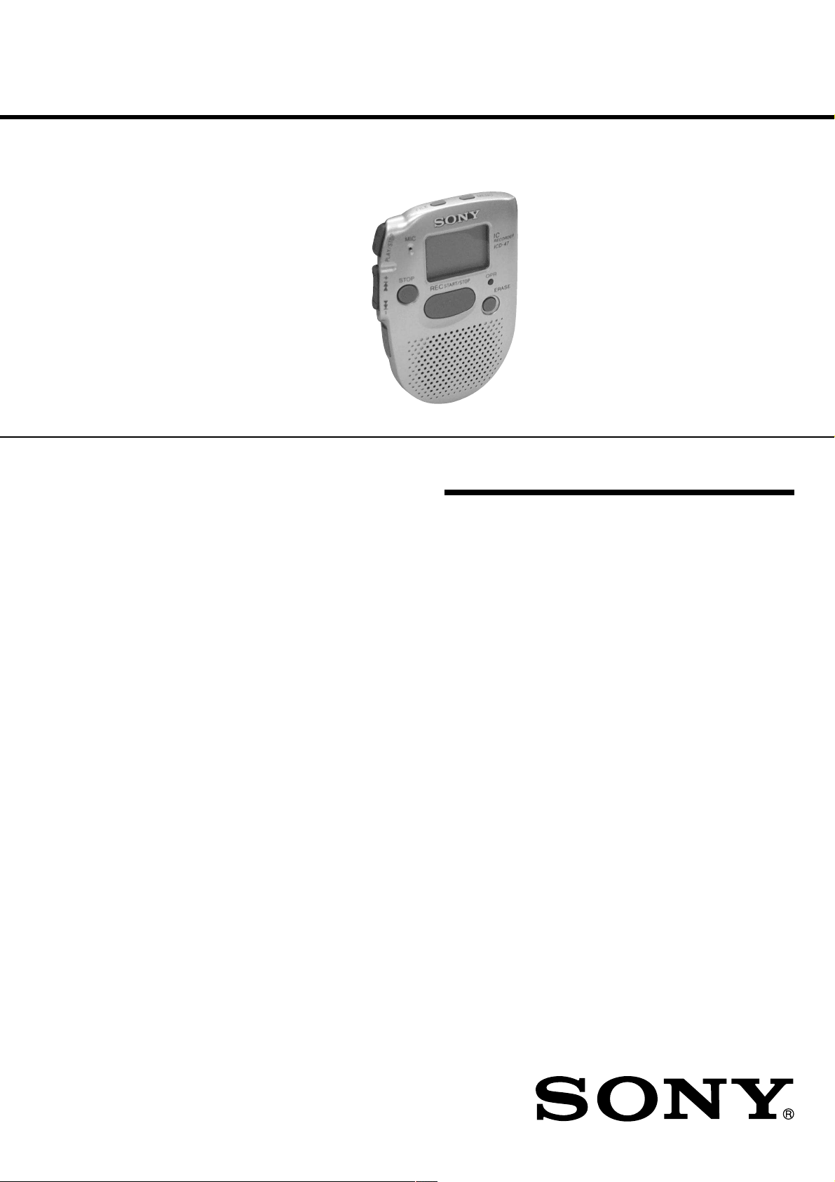
ICD-47
SERVICE MANUAL
Ver 1.0 2001.04
SPECIFICATIONS
Recording media Built-in flash memory, Monaural recording
Recording time 90 minutes
Frequency response 280 Hz - 2 800 Hz
Speaker approx. 3.6 cm (1
Power output 80 mW
Output Earphone jack (mini jack) for 8 - 300 Ω earphone
Playback speed control FAST: +50%
SLOW: –25%
Power requirements One LR03 (size AAA) alkaline battery: 1.5 V DC
Dimensions (w/h/d) (not incl. projecting parts and controls)
58.0 × 83.5 × 14.2 mm (2
Mass (incl. battery) 56 g (1.98 oz)
Design and specifications are subject to change without notice.
7
⁄16 in.) dia.
3
3
9
⁄
8
× 3
⁄
8
×
⁄16 in.)
US Model
Canadian Model
AEP Model
UK Model
E Model
Features
• 90 minutes recording time
This unit is useful for recording messages or appointments.
• Organizing message files
You can choose among 3 different files to record and store your
messages.
You can easily move messages from one file to another (see page 18).
Up to 99 messages can be recorded in each file.
• Alarm function
You can start playing back a desired message with an alarm on a desired
date and time (see page 21). You can use this function to remind you of
the time of the meeting, etc.
• Playback speed control
• Adding a recording to previously recorded message
9-873-119-11 Sony Corporation
2001D0500-1 Personal Audio Company
C 2001.4 Shinagawa Tec Service Manual Production Group
You can play back messages rapidly (+50%) or slowly (–25%) (see page
19). This is useful when playing back a long recording. The sound pitch
will be automatically adjusted when you change the playback speed.
You can add a recording to the message being played back to count as
one message (see page 20).
IC RECORDER
Page 2

ICD-47
SECTION 1
SERVICING NOTES
TABLE OF CONTENTS
1. SERVICING NOTES............................................... 2
2. GENERAL ................................................................... 3
3. DISASSEMBLY
Disassembly Flow ........................................................... 4
Lid, Battery Case ............................................................ 4
“Case (Front) Section”, “Case (Rear) Section” ............. 4
MAIN Board ................................................................... 5
Installation “MAIN Board”,
“Microphone, Electric Condenser” (MIC101) ............... 5
4. TEST MODE .............................................................. 6
5. DIAGRAMS
5-1. Block Diagram ................................................................ 7
5-2. Printed Wiring Board ...................................................... 8
5-3. Schematic Diagram ......................................................... 9
5-4. IC Pin Function Description ........................................... 12
6. EXPLODED VIEW................................................... 15
7. ELECTRICAL PARTS LIST ............................... 16
CAUTION ON REPLACING FLASH MEMORY
The BAD-BLOCK check* must be executed, when the flash
memory (IC702) in this set was replaced.
The set will not operation normally, unless this check is finished.
* The BAD-BLOCK check detects an area (bad-block) in the flash
memory where data validity cannot be guaranteed, and saves this
information in the TOC-AREA so that a bad-block is not used.
BAD-BLOCK check Procedure:
1. Apply 1.5 V from re gulated power supply to the battery terminals.
2. Once the po wer is supplied, the check starts and then proceeds
for approx. 45 seconds. (Be sure to keep applying the power
and pin yj or TP13 (green)/Pin yh or TP14 (red) signal “H”
during the check)
* Green/red LED of
it cannot be seen visually. Check the signal of pin yh , yj or
TP13, 14.
3. When the check completes, the result is shown as follows.
OK:Pin yh or TP14 signal “L” (Pin yj or TP13 Signal “H”)
NG:Pin yj or TP13 signal “H” (Pin yh or TP14 signal “L”)
4. In case of OK, press the
Note:
• In case of NG, check system controller IC (IC701), flash memory IC
(IC702) and the peripheral circuit. (Particularly , check carefully the soldering of the flash memory)
• After finishing the BAD-BLOCK check, assemble the set, load the dry
battery, and confirm if the set operates normally.
[OPR] indicator don't light up, therefore
[STOP] button.
Notes on chip component replacement
• Never reuse a disconnected chip component.
• Notice that the minus side of a tantalum capacitor may be damaged by heat.
Flexible Circuit Board Repairing
• Keep the temperature of the soldering iron around 270 ˚C during repairing.
• Do not touch the soldering iron on the same conductor of the
circuit board. (within 3 times)
• Be careful not to apply force on the conductor when soldering
or unsoldering.
2
Page 3
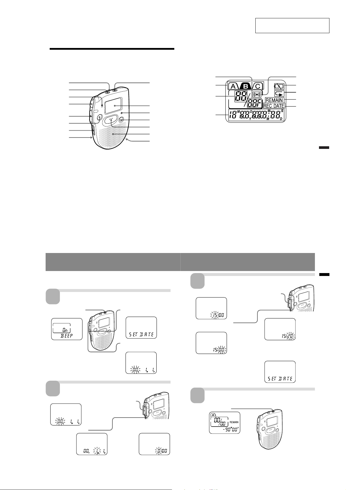
Index to Parts and Controls
Refer to the pages indicated in parentheses for details.
Main unit
1
2
3
4
5
6
7
8
1 VOL (volume) control (14)
2 FILE button (10, 13, 18)
3 MIC (built-in microphone)
(10)
4 NxPLAY/STOP (play/
stop•enter) button (8, 14, 15)
5 –./>+ (fast forward/
fast backward•selection of
menu mode) button (13, 15)
6 STOP button (11)
7 HOLD switch (25)
8 PLAY SPEED selector (19)
9 MENU button (8, 21, 34)
0 Display window (33)
qa OPR (operation) indicator
(10, 14)
qs ERASE button (16)
qd REC (record) START/STOP
button (10)
qf Speaker
qg EAR (earphone) jack (15)
SECTION 2
GENERAL
9
q;
qa
qs
qd
qf
qg
Display window
2
3
4
1 Total number of messages in
a file (13)
Mode indication of the
menu(21, 26 - 28) (On, OFF,
etc.)
2 File indication (10, 13)
3 Current message number (10,
13)
4 Remaining recording time
indication (10)
Recording date indication
(14)
Current time/day indication
(8)
Menu indication (8, 21, 26 28, 34) (ALARM, etc.)
Messages (ERASE, SCAN,
etc.)
ICD-47
This section is extracted from
instruction manual.
51
6
7
8
9
5 Alarm indicator (23)
6 Battery exhausted indicator
(7)
7 Repeat play indicator (15)
8 REMAIN indication (10)
9 REC DATE indication (14)
Additional Information
32
Step 2: Setting the Clock
Clock setting display appears when you insert battery for the first time, or
when you insert battery after the unit has been without battery for a
certain period of time. In this case, proceed from Step 2.
Display the clock setting display.
1
1 Press MENU to enter
the menu mode.*
* The “ALARM” display may
appear instead of the “BEEP”
display (see page 34).
Set the date.
2
1 Press –. or >+ to select the digits of the year.
2 Press –. once to display
“SET DATE”.
3 Press NxPLAY/STOP.
The year digits will flash.
Set the time.
3
1 Press –. or >+ to select the digits of the hour.
3 Set the minute.
2 Press NxPLAY/STOP.
The minute digits will flash.
4 Press NxPLAY/STOP at the
time signal.
The display will return to
“SET DATE”.
Exit from the menu mode.
4
Press MENU.
33
Getting Started
2 Press NxPLAY/STOP.
The month
digits will flash.
8
3 Set the month and day in
sequence, then press
NxPLAY/STOP.
The hour
digits will
flash.
9
3
Page 4
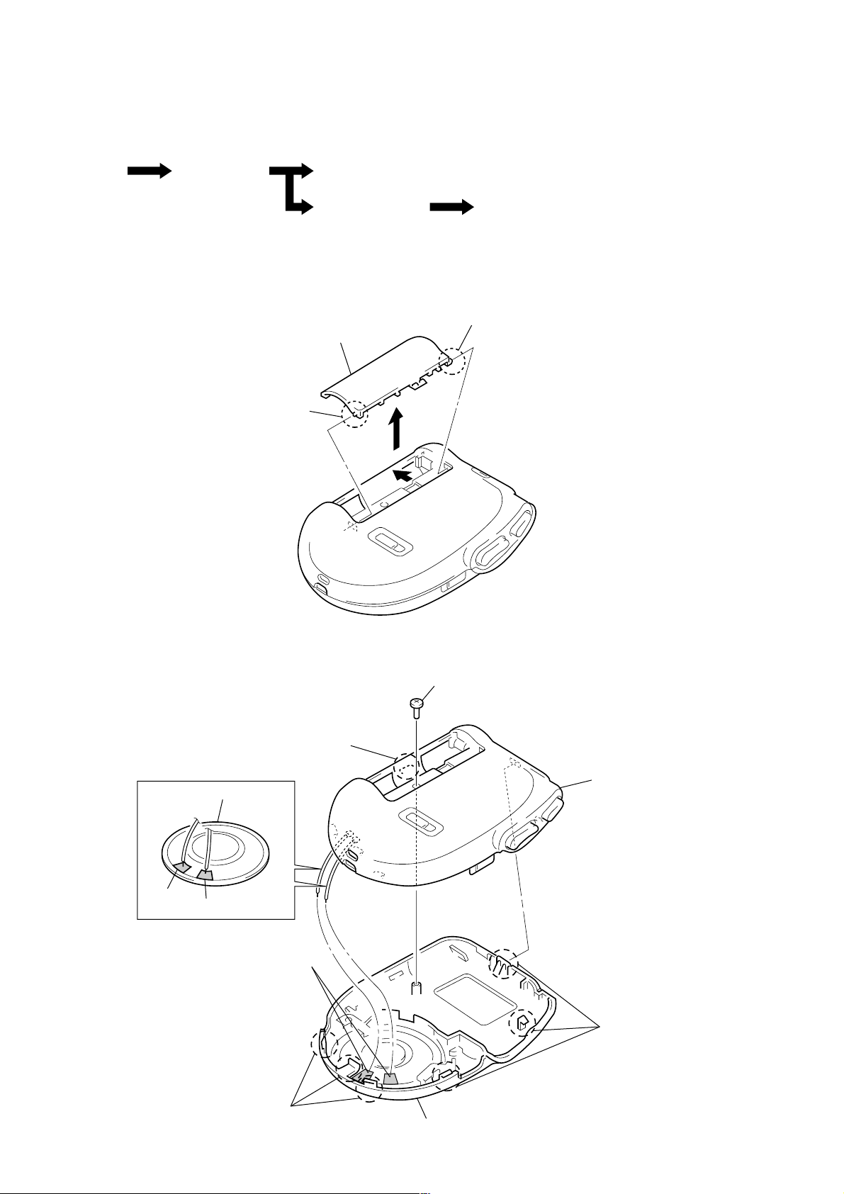
ICD-47
)
• This set can be disassembled in the order shown below.
DISASSEMBLY FLOW
SECTION 3
DISASSEMBLY
Set
Note: Follow the disassembly procedure in the numerical order given.
Lid, Battery Case
Case (Front) Section
Case (Rear) Section Main Board
Installation “Main Board”, “Microphone, Electric Condenser” (MIC101
LID, BATTERY CASE
3 lid, battery case
2 boss
2 boss
1
“CASE (FRONT) SECTION”, “CASE (REAR) SECTION”
2 claw
speaker (SP101)
#
3
3 Remove the two solders
speaker lead (SP101).
1 screw
5 case (rear) section
2 three claws
2 three claws
4 case (front) section
4
Page 5
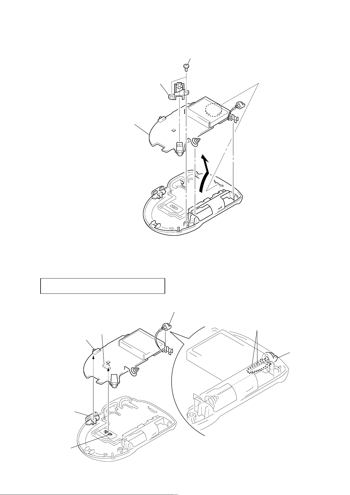
MAIN BOARD
r
ICD-47
1 two screws
(M1.7 × 4)
2 bracket
(jack)
3 Remove the MAIN board to
direction of the arrow.
INSTALLATION “MAIN BOARD”, “MICROPHONE, ELECTRIC CONDENSER” (MIC101)
Note: On installation MAIN board adjust the S711, S712
and knob (HOLD, MODE).
microphone, electric condenser
(MIC101)
S712
S711
knob (HOLD)
Install two leads the electric condenser microphone
(MIC101) in the figure.
two leads
microphone,
electric condense
(MIC101)
knob (MODE)
5
Page 6
ICD-47
SECTION 4
TEST MODE
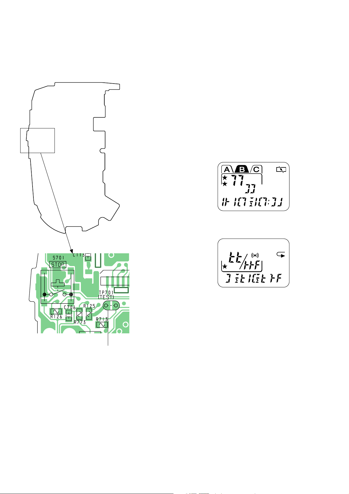
[Setting Method of Test mode]
Short TP701 (TEST) on the MAIN board with a solder bridge (connect pin yf of IC701 to the ground). Then, turn on the power.
– MAIN BOARD (Side A) –
1. Audio test
• A howling occurs with “5P DSP LOOP” displayed on the LCD,
if the [REC START/STOP] key is pressed.
• The mute turns on, if [ +] key is pressed.
• The mute turns off, if [-- ] key is pressed.
• The microphone sensitivity becomes high, if the [HOLD] switch
turned off.
• The microphone sensitivity becomes lo w, if the [HOLD] switch
turned on.
2. Sleep/Wake up test
• Pressing the [ ] key causes the set to enter sleep state.
• Pressing another key causes the set to release sleep state.
3. LCD check
• LCD light up all, if the [STOP] key is pressed.
• Even segment of LCD light up as shown below, if the [FILE]
key is pressed.
LCD display
Nx
>
.
REC DATE
M
D
M
Y
M
S
D
Short : Test mode
Open : Normal mode
[Releasing Method of Test Mode]
Turn of f the power . Then, open the solder bridge on TP701 (TEST)
on the MAIN board.
TP701
)(
• Odd segment of LCD light up as shown below, if the [ERASE]
key is pressed.
LCD display
SP
LP
REMAIN
4. Beep sound check
• A beep (2.4 kHz) is kept sounding, if the
• A beep stop sounding, if another key is pressed.
5. Power supply check
• The battery is on the O.K. level when the [OPR] LED lights in
green only, or it is off.
• The battery is on the mark lighting level when the [OPR] LED
lights in green and blinks in red repeatedly.
• The battery is on the inactive le v el when the [OPR] LED blinks
in red only.
[MENU] key is pressed.
[Operation of Setting on Test Mode]
When the test mode is set, the LCD displays “TEST” and [OPR]
LED lights in green.
Note: The [OPR] LED turn off, if a key operated.
6
Page 7

5-1. BLOCK DIAGRAM
ICD-47
SECTION 5
DIAGRAMS
MIC101
MIC
ADPCM
IC101 (1/2)
TI–
18 13 40
MIC SENSE
SWITCH
Q103
MIC AMP
IC103
L. P. F
AGC
IC107
H. P. F
A/D
CONVERTER
FLASH MEMORY
(32BIT)
IC702
TRANSMIT
SHIFT
REGISTER
SEQUENCE
AND
CONTROL
BCLKR
MCLK
BCLKT
FSR
FST
DT
9
11
12
7
14
X701
32.768kHz
DIGITAL SIGNAL
PROCESSOR
IC104 (1/2)
SDI
SCLK
42
SLDA
43
REAL TIME CLOCK
9
OSCIN
8
SOCOUT
1 6
32KOUT INTR
37
IC703
MDISD0
SCK
SSN
IOPD0
IOPD1
DAV
RDY
RSTB
SI
SO
SCLK
CE
16
18
19
29
28
36
2
RESET
SWITCH
Q111
4
3
2
7
DIGITAL SIGNAL
SYSTEM CONTROLLER
IC701
72 73 72 41 8 2
DSPSI
74
DSPSCK
DSPSSN
16
85
DSPFRM
DSPSTP
65
DSPDAV
89
DSPRDY
88
DSPRST
71 21
76
RTCDO
75
RTCDI
77
RTCCLK
70
RTCCE
87
RTCINT
82
XT1
DSPSO
LMUTE
BEEP
LEDPB
LEDREC
5
32 – 6123 – 26
S0 – S29COM0 – COM3
67
66
CRYSTAL
DISPLAY
PROCESSOR
IC104 (2/2)
DSPSI SDO
XTALA
32
ND701
LIQUID
LED DRIVE
Q506 (1/2)
LED DRIVE
Q506 (2/2)
ADPCM
IC101 (2/2)
DR
LINE MUTING
Q105
D504
OPR
RECEIVE
REGISTER
GRN
(PLAY)
RED
(REC)
SHIFT
D/A
CONVERTER
+
L. P. F
POWER AMP
IC102, Q108, 109
RO–
RV101
VOL
J101
v
(SPEAKER)
• SIGNAL PATH
: PLAY
: REC
SP101
S701
S702
S703
S704
S705
MICSEL
STOP
REC
START/STOP
PLAY/STOP
Nx
(EXECUTE)
– .
> +
(SELECT)
S701 – 705 S707 – 709
I/O0 – I/O7
18 – 21, 24 – 27
91 – 98
FMIO0 – FMIO7
KEY0
1 2 86 4 3 64
KEY1
RE
WE
ALE
CLE
XFMRE
XFMWE
XFMALE
XFMCLE
WAKE UP CONTROL
SWITCH
Q701 – 703
MENU
S707
FILE
S708
ERASE
S709
WP
GND
XFMSE
XFMWP
R/B
CE
414354042432
1371920171011146
XFMCE
XFMBSY
WAKEUP
S711
OFF
HOLD
XHOLD
SPDSW
S712
PLAY SPEED> HOLD
FAST
NORMAL
SLOW
X702
5MHz
XTEST
(TEST)
TP701
X2
79
X1
80
15
DSPMCK Q0CLKIN
AMPPOW
PLLCRL
APOWER
XSPOWER
XRESET
BATT
100
3 6
68
22
63
69
84
DIVIDER
IC106
CE
4
POWER
SWITCHING
Q508
BATT B+
1.5V
(POWER AMP (IC102) B+)
ADPCM (IC101), DSP (IC104),
SYSTEM CONTROLLER (IC701), FLASH
MEMORY (IC702), REAL TIME CLOCK (IC703) B+
3.3V
DIVEDER (IC106), LED B+
3.3V
MIC AMP (IC103),
AGC (IC107) B+
3.3V
REGULATOR
REGULATOR
RESET SIGNAL
GENERATOR
IC505
+3.3V
IC503
+3.3V
IC506
B+ SWITCH
Q106, 107
DC/DC
CONVERTER
IC502, Q502
DC/DC
CONVERTER
IC501
BATT B+
DC/DC CONVERTER
CONTROL
Q507
DRY BATTERY
(IEC DESIGNATION R03)
VOLTAGE
DETECT
IC504
SIZE "AAA"
1PC. 1.5V
77
Page 8

ICD-47
• Semiconductor
Location
Ref. No. Location
D501 E-2
D502 D-2
D504 C-4
D701 E-3
IC101 B-4
IC102 F-3
IC103 C-9
IC104 B-3
IC106 C-3
IC107 B-2
IC501 F-2
IC502 E-2
IC503 E-2
IC504 D-3
IC505 F-3
IC506 D-2
IC701 D-8
IC702 F-8
IC703 E-4
5-2. PRINTED WIRING BOARD
12345678910
A
B
C
Q103 B-9
Q105 F-2
Q106 F-2
Q107 F-9
Q108 F-3
Q109 G-2
Q111 B-8
Q502 D-2
Q506 D-4
Q507 D-3
Q508 F-9
Q701 F-2
Q702 F-2
Q703 F-2
D
G
E
F
v
Note on Printed Wiring Board:
• X : parts extracted from the component side.
• Y : parts extracted from the conductor side.
f
•
• : Pattern from the side which enables seeing.
(The other layers' patterns are not indicated.)
Caution:
Pattern face side: Parts on the pattern face side seen from
(Side B) the pattern face are indicated.
Parts face side: Parts on the parts face side seen from
(Side A) the parts face are indicated.
• Main board is four layer printed board.
: internal component.
However , the patterns of layers 2 and 3 ha ve not been included
in this diagrams.
88
Page 9

5-3. SCHEMATIC DIAGRAM • See pag e 10 for IC Block Diagrams. • See page 11 for Waveforms.
ICD-47
MIC101
INVA_IN
INVB_IN
VIN
V
6.3
47
C508
470k
R515
C126
IC102
NJM2076
NON
VDD
BASE_B
POWER AMP
2SB1073
B+ SWITCH
NC
TP54TP55
TP52
BASE_A
A_OUT
VSS
B_OUT
Q106
S
VOUT
NC
VIN
FB504
10
10
NC CEVOUT
2
VSS
51
C
C507
FB503
C504
47
6.3V
C503
47
6.3V
R101
2.2k
TP58
MIC
UN9213J
TP59
6.3V
22
100p
102
C
C101
R751
10k
R706
100k
Q701,702
WAKE UP
CONTROL
SWITCH
Q701
R772
470k
TP24
0.5%
C706
0.1
S701
STOP
TP20
S3
S2
S1
S0
S4
C104
0.033
C120
0.1
P103
P101
P100
P34
FMIO0
FMIO1
FMIO2
FMIO3
Q702
2SB1218A
4.7k
0.5%
REC
START/STOP
S5
MIC AMP
IC103
LMV751M5X
S702
S6
R102
330
V+
R707
10k
0.5%
S703
S703S702
PLAY/STOP
(EXECUTE)
S9
S8
S7
S10
TP57
V-
VSS
CEL
AEL
WE
WP
NC
NC
NC
NC
NC
NC
NC
NC
NC
NC
NC
NC
I/O0
I/O1
I/O2
I/O3 I/O4
VSS VCC
K9F3208WOA-TCBOT
FLASH MEMORY
R708
470k
0.5%
R775R774R773
15k
0.5%
S13
S12
S11
LIQUID CRYSTAL DISPLAY
R143
47k
C114
10
16V
C136
100p
R144
47k
VCC
CE
RE
B
R/
GND
NC
NC
NC
NC
NC
NC
NC
NC
NC
NC
NC
NC
I/O7
I/O6
I/O5
IC702
R771
33k
TP22
0.5%1M
R776
22k
TP27TP26TP25
0.5%
S704
S704 S705
(SELECT)
S16
S15
S14
ND701
R115
1M
R146
22k
0.047
TP106
TP21
TP8
705
S
S18
S17
VCCDET
S23
R158R145
3.3k10k
C155
0.22
FMIO7
FMIO6
FMIO5
FMIO4
2SB1218A
WAKE UP
CONTROL
SWITCH
AGC
IC107
AN6123MS
TP105
C144C113
R116
10k
0.10.047
47k
R154
R153
47k
R151
HOLD OFF
TP33
COM2
COM1
10k
R108
10k
HOLD
S711
T)
S
(TE
701
TP
711
0.1
C
COM3
W701
C143
Q103
UN9211J
MIC
SENSE
SWITCH
P17
P32
P102
P35
33k 0.5%
R777
Q703
R779
4.7k
TP30
0.5%
S26
S25
S24
0.1
C142
0.01
C751
0.1
R752
100k
C752
47
6.3V
1k
711
R
R781
10k
TP31
0.5%
S709S708
ERASEFILEMENU
S29
S28
S27
COM0
MCLK
PDI
BCLKT
BCLKR
DR
DT
FSR
FST
VDDVSS
PO+MU/A
PO-
TG
PITI-
RO-TI+
VAG
VAGREF
IC101
MC145481
ADPCM
10k
R770
R782R713R712
220k680k680k
S712
TP35
708
C
0.01
PLAY SPEED
FAST
NORMAL
TP36
784
R
220k
SLOW
TP7
A2
A3
A4
P17
P100
P101
P102
P103
SSN
P32
P34
P35
COM0
COM1
COM2
C761
0.1
RDY
R152
47k
R156
47k
C149
0.1
R124
10k
4700p
R125
C121
33
C705
KEY0
KEY1
SPDSW
XHOLD
LMUTE
MICSEL
XFMCE
VDD0
AVREF
XFMWE
XFMALE
VSS1
XFMBSY
XFMCLE
DSPMCK
DSPSSN
XFMRE
NC
XFMWP
XFMSE
BEEP
PLLCRL
COM0
COM1
COM2
COM3
VDD
RDY
SLDB
OSCBYP
INTB
IOPA7
IOPA6
IOPA5
IOPA4
IOPA3
IOPA2
1
FMIO7
S
TT
S
A
V
B
A
3
M
O
IAS
C
B
220k
701
R
IN GND DET
C139
R709
1M
R710
470k
0.5%
R778
470k
TP6
0.5%
0.1
S707
707
C
+-
S21
S20
S22
S19
R157
3.3k
R161C157
1M0.1
A4
A3
A2
A1
I
A
S
S
V
S
S
V
FMIO5
FMIO6
7
6
IO
IO
M
M
F
F
0
1
C
C
L
L
V
V
702
220k
R
S
O
D
LK
S
D
S
C
LD
V
S
S
S
DIGITAL
SIGNAL
PROCESSOR
IC104
1609J--VA11H-DB
I
D
1
0
S
A
A
O
D
P
P
D
D
IO
V
MDISDO
M
IO
DI
DO
IO1
FMIO2
FMIO0
FMIO3
FM
FMIO4
5
3
4
2
1
IO
IO
IO
IO
IO
M
M
M
M
F
F
FM
F
F
S0
C2
L
2
1
0
S
V
S
S
S
V
703
S1
S3
S0
S2
R
220k
V
B
D
T
A
D
S
D
V
R
K
N
O
C
S
D
T
S
S
SSN
SCK
RDY
DAV
0
V
EF
A
IO
R
D
V
P
FM
A
S
D
SYSTEM CONTROLLER
IC701
µPD780308GC-A31
-8EU
4
3
5
S
S
S
S6
S5
S4
Q111
UN9214J
RESET
SWITCH
P
A
P
D
V
VD
VSSA
XTALA
XTALB
VSS
IOPD0
IOPD1
RWN
IOPD3
TMS
TCK
VDD
S
I
S
D
V
T
R761
470k
FRM
T
Y
P
M
ET
D
IN
XT2
S
EU
FR
C
E
PR
T
R
AK
S
SP
R
X
D
D
W
1
0
1
8
7
6
S
S1
S
S9
S
S
S12
S9
S11
S8
S10
S7
1
T
X
2
1
S
C146
R765R762
10k470k
1
D
D
V
3
1
S
S13
22p
FRM
STOP
REAL TIME CLOCK
X702
5MHz
2
1
X
X
4
15
1
S
S
S15
S14
RST
DAVA1
C147
0.1
IC
RTCDO
LK
C
TC
R
RTCDI
DSPSCK
DSPIO
DSPSI
DSPRST
RTCCE
XSPOWER
AMPPOW
LEDPB
LEDREC
DSPSTP
XTEST
APOWER
NC
S29
S28
S27
S26
S25
S24
S23
S22
S21
S20
S19
8
6
1
17
S
S
S1
S17
S16
S18
DIVIDER
IC106
XC25BS5001MR
Q1
Q0
VDD
VSS
CLKIN
CE
C154
0.1
R165
100k
Q105
DTC363EKT146
LINE MUTING
C127
0.1
IC703
RS5C348A
VDD
32K
OUT
OSC
SCLK
IN
SO
OSC VSS CE
OUT
SI
VSSCEINTR
X701
k
32.768 Hz
TP12
C702
68
6.3V
SCK
DI
DO
RST
TP13
TP14
STOP
S29
S28
S27
S26
S25
S24
S23
S22
S21
S20
S19
R140
4.7k
C129
0.1
R155
10k
C160
0.033
10V
52
.1
10
0
1SS3
153
701
C
C
D701
TP46
R783
100k
-1 -2
GRN RED
R509
100k
R510
1k
C505
0.1
OUT
10V
10
510
C
(REC)(PLAY)
-1 -2
L903
10µH
C128
47
6.3V
R137
47k
R517
100
IC506
XC62G3312MR
+3.3V
REGULATOR
SWITCHING
3LN01S
R512R553
2.2k680
TP4TP3
IN
IC505
XC61AN3002MR
RESET SIGNAL
GENERATOR
R551
470k
POWER
Q508
D504
CL155UR
OPR
2SA11821k
DRIVER
C133
1
Q508
XP1212
LED DRIVE
Q109R126
REGULATOR
XC62G3312MR
Q506
+3.3V
IC503
VOUT
VSS CE
S
GND
R134
100
B+ SWITCH
C506
2SK2036
R505
470k
LX
0p
100
Q107
R502
1.5k
-1
R133
470k
TP47
Q507
XP4601
DC/DC
CONVERTER
CONTROL
OUT
D502
RB551V
DC/DC
CONVERTER
IC501
XC6372C331PR
-2
C134
XC61AN0802
VOLTAGE
DETECT
CONVERTER
XC6372D351PR
Q502
CPH3209
DC/DC
CONVERTER
IC504
DC/DC
22
4V
IN
IC502
Q108
2SA1182
DRIVER
-1 -2
RV101
10k/10k0.047
VOL
TP41
R508 C511
470k 0.1
GND
NCVOUT CE
VSS LX
C130
0.1
C131
0.47
C132 R132
0.47 1
TP9
R506
1M
W101
W102
(SPEAKER)
DRY BATTERY
SIZE"AAA"
IEC DESIGNATION
R03
1PC.1.5V
SP101
J101
)(
TP51
R131
TP49
1
FB131
FB132
TP10
R136
22
C135
22
4V
R507
220k
R716
1k
L502
P01
T
W501
C550
10
W502
TP02
L501
47µH
D501
RB551V
Note on Schematic Diagram:
• All capacitors are in µF unless otherwise noted. pF: µµF
50 WV or less are not indicated except for electrolytics
and tantalums.
• All resistors are in Ω and 1/
specified.
4
W or less unless otherwise
• % : indicates tolerance.
f
•
: internal component.
• C : panel designation.
• A : B+ Line.
• Po wer voltage is dc 1.5 V and fed with regulated dc pow er
supply from battery terminal.
• Voltages and waveforms are dc with respect to ground
under no-signal conditions.
no mark : PLAY
( ) : REC
: Impossible to measure
∗
• V oltages are taken with a VOM (Input impedance 10 MΩ).
Voltage variations may be noted due to normal production tolerances.
99
• Waveforms are taken with a oscilloscope.
Voltage variations may be noted due to normal production tolerances.
• Circled numbers refer to waveforms.
• Signal path.
F : PLA Y
L : REC
Page 10

ICD-47
• IC Block Diagrams
IC101 MC145481SDR2
VAG REF
1
RO–
PO–
PO+
VDD
FSR
BCLKR
PDI
2
PI
3
4
5
6
7
DR
8
9
10
L. P. F.
CUT OFF
FREQUENCY: 3.4 kHz
–
+
–1
RECEIVE SHIFT
REGISTER
VDD
VSS
H. P. F.
CUT OFF
FREQUENCY: 200 Hz
SHARED
DAC
0.886 V
REF
DAC ADC
SEQUENCE
AND
CONTROL
1
L. P. F.
CUT OFF
FREQUENCY: 3.4 kHz
TRANSMIT SHIFT
REGISTER
IC501 XC6372C331PR
IC503, 506 XC62GR3312MR
IC502 XC6372D351PR
VSS
1
VIN
SLOW
VDD
START
REFERENCE
VOLTAGE
CHIP
ENABLE
PHASE
COMPARATOR
–
+
VLX
LIMITER
PWM/PFM
CONTROL
OSC 100kHz
BUFFER
VAG
20
1
NC
2
+
TI+
19
–
TI–
18
TG
17
MU/A
16
VSS
15
FST
14
DT
13
BCLKT
12
MCLK
11
VOUT
CE
3
VSS
5
LX
4
2 5
CURRENT
LIMIT
+
–
CE
OUTPUT
3
CONTROL
REFERENCE
VOLTAGE
VOUT
NC
4
IC703 RS5C348A-E2
IC102 NJM2076M (TE2)
INVA IN
NON INVB IN
VDD
BASE B
1
2
3
4
POWER
AMP
POWER
AMP
IC107 AN6123MS-TXL
DET
5
GM
GND
4
DET
32KOUT
1
IC106 XC25BS5001MR
11 BIT PLL
BASE A
8
A OUT
7
VSS
6
5
B OUT
IN
3
Q1
VDD
CLKIN
1
1
2
2
3
(×N)
1
4
Q0
6
VSS
5
CE
4
SCLK
VSS
2
SO
3
4
SI
5
32 kHz
OUTPUT
CONTROL
I/O
CONTROL
COMPARATOR
COMPARATOR
ADDRESS
REGISTER
SHIFT
REGISTER
ALARM W REGISTER
ADDRESS
DECODER
INTERRUPT
CONTROL
VOLTAGE
DETECT
(WEEK, MIN, HOUR)
ALARM D REGISTER
W
D
TIMER COUNTER
SEC, MIN, HOUR, WEEK,
DAY, MONTH, YEAR
(MIN, HOUR)
DIV
DIVIDER
CORRECTION
OSC
DETECT
OSC
VDD
10
9
8
7
6
VDD
OSCIN
OSCOUT
CE
/INTR
1
VCC
2
DET
1010
Page 11

• Waveforms
ICD-47
1 IC101 7 (FSR), qf (FST)
IC104 rd (SLDA)
1 V/DIV , 50 µs/DIV
150 µs
2 IC101 9 (BCLKR), qa (MCLK),
qs (BCLKT), IC104 rs (SCLK)
1 V/DIV, 200 ns/DIV
3.4 Vp-p
3.4 Vp-p
5 IC701 ul (X2)
2 V/DIV, 100 ns/DIV
3.6 Vp-p
200 ns
6 IC701 is (XT1), IC703 1 (32KOUT)
1 V/DIV, 10 µs/DIV
2.5Vp-p
9 IC501 4 (LX)
1 V/DIV, 5 µs/DIV
4.3 Vp-p
9.9 µs
0 IC502 4 (LX)
2 V/DIV, 5 µs/DIV
3.6 Vp-p
565 ns
3 IC104 es (XTALA), IC106 6 (Q0)
1 V/DIV, 100 ns/DIV
4.6 Vp-p
282 ns
4 IC106 3 (CLKIN), IC701 qg (DSPMCK)
1 V/DIV , 20 µs/DIV
3.4 Vp-p
30.6 µs
7 IC701 ij (RTCINT), IC703 6 (INTR)
2 V/DIV, 200 ms/DIV
4.3 Vp-p
500 ms
8 IC703 8 (OSCOUT)
200 mV/DIV, 10 µs/DIV
1.1 Vp-p
11.2 µs
qa Q502 (Base)
200 mV/DIV, 5 µs/DIV
0.9 Vp-p
11.1 µs
qs Q502 (Collector)
1 V/DIV, 5 µs/DIV
4.6 Vp-p
73.5 µs
30.6 µs
3.6 µs
11
Page 12

ICD-47
5-4. IC PIN FUNCTION DESCRIPTION
• IC104 1609J--VA11H-DB (DIGITAL SIGNAL PROCESSOR)
Pin No. Pin Name I/O Description
1VDD—
2 RDY O
3 SLDB I/O
4 OSCBYP I
5 INTB I
6 to 11 IOPA7 to IOPA2 I/O
12 VSS —
13 VDD —
14, 15 IOPA1, IOPA0 I/O
16 MDISDO O
17 MDISDI I
18 SCK I
19 SSN I
20 TDO O
21 TDI I
22 VSS —
23 VDD —
24 TCK I
25 TMS I
26 IOPD3 I/O
27 RWN O
28 IOPD1 I
29 IOPD0 O
30 VSS —
31 XTALB I/O
32 XTALA I
33 VSSA —
34 VDDA —
35 VPP —
36 DAV O
37 RSTB I
38 VDD —
39 VSS —
40 SDI I
41 SDO O
42 SCLK O
43 SLDA O
44 VSS —
Power supply terminal (+3.3V)
Interrupt output terminal of ready/busy detection signal to the system controller (IC701)
“L”: ready, “H”: busy
Not used (open)
Not used (fixed at “H”)
Not used (open)
Not used (open)
Ground terminal
Power supply terminal (+3.3V)
Not used (open)
Recording serial data output to the system controller (IC701) “H” active
Playback serial data input from the system controller (IC701) “H” active
Serial clock signal input from the system controller (IC701) “H” active
Transmission status input from the system controller (IC701) “L” active
Not used (open)
Not used (open)
Ground terminal
Power supply terminal (+3.3V)
Not used (open)
Not used (open)
Not used (open)
Not used (open)
Stop signal input from the system controller (IC701) “L” active
Interrupt output terminal of frame signal to the system controller (IC701) “H” active
Ground terminal
Not used (fixed at “L”)
PLL clock signal (4.096 MHz) input from the divider (IC106) “H” active
Ground terminal
Power supply terminal (+3.3V)
Not used (open)
Available data output to the system controller (IC701) “H” active
Reset signal and power down detection signal input from the system controller (IC701)
“L”: reset or power down
Power supply terminal (+3.3V)
Ground terminal
Recording serial data input from the ADPCM (IC101)
Playback serial data output to the ADPCM (IC101)
Serial clock signal output to the ADPCM (IC101)
Serial data output to the ADPCM (IC101)
Ground terminal
12
Page 13

• IC701 µPD780308GC-A31-8EU (SYSTEM CONTROLLER)
Pin No. Pin Name I/O Description
1 KEY0 I
2 KEY1 I
3 SPDSW I
4 XHOLD I
5 LMUTE O
6 MICSEL O
7 XFMCE O
8 VDD0 —
9 AVREF I
10 XFMWE O
11 XFMALE O
12 VSS1 —
13 XFMBSY I
14 XFMCLE O
15 DSPMCK O
16 DSPSSN O
17 XFMRE O
18 NC —
19 XFMWP O
20 XFMSE O
21 BEEP O
22 PLLCRL O
23 to 26 COM0 to COM3 O
27 BIAS O
28 to 30 VLC0 to VLC2 I
31 VSS0 —
32 to 61 S0 to S29 O
62 NC —
63 APOWER O
64 XTEST I
65 DSPSTP O
66 LEDREC O
67 LEDPB O
68 AMPPOW O
69 XSPOWER O
70 RTCCE O
71 DSPRST O
Key input terminal (A/D input) S701 to S705 (STOP, REC START/STOP, Nx PLAY/STOP
(EXECUTE), – . (SELECT), > + (SELECT) ) keys input
Key input terminal (A/D input) S707 to S709 (MENU, FILE, ERASE) keys input
PLAY SPEED select switch (S712) input terminal (A/D input)
“L”: SLOW, “M”: FAST, “H”: NORMAL
HOLD switch (S711) input terminal “L”: HOLD ON, “H”: HOLD OFF
Line muting control signal output terminal “H”: line muting on
Microphone sensitivity select signal output terminal
“L”: mic sensitivity low, “H”: mic sensitivity high
Chip enable signal output to the flash memory (IC702) “L” active
Power supply terminal (+3.3V)
Reference voltage input terminal (for A/D converter)
Write enable signal output to the flash memory (IC702) “L” active
Address latch enable signal output to the flash memory (IC702) “L” active
Ground terminal
Ready/busy detection signal input from the flash memory (IC702) “L” active
Command latch enable signal output to the flash memory (IC702) “L” active
Sampling frequency sync signal output to the digital signal processor (IC104) “H” active
Transmission status output to the digital signal processor (IC104) “L” active
Read enable signal output to the flash memory (IC702) “L” active
Not used (open)
Write protect signal output to the flash memory (IC702) “L” active
Spare space enable signal output to the flash memory (IC702) “L” active
Beep sound drive signal output terminal (2.4 kHz) “H” active
Serial data transfer clock signal output to the divider (IC106)
Power on/off control signal output for the ADPCM (IC101), digital signal processor (IC104),
divider (IC106) and LED power supply “H”: power on
Common drive signal output to the liquid crystal display (ND701) “H” active
Power supply output terminal for the liquid crystal display (ND701) “H” active
Power supply input terminal for the liquid crystal display (ND701) “H” active
Ground terminal
Segment drive signal output to the liquid crystal display (ND701) “H” active
Not used (open)
Power on/off control signal output for the mic amplifier (IC103) and AGC (IC107)
“H”: power on (rec mode)
Setting terminal for the test mode “L”: test mode (Normally: fixed at “H”)
Stop signal output to the digital signal processor (IC104) “L” active
LED drive signal output of the REC indicator (D504 red) “H”: LED on (rec mode)
LED drive signal output of the PLAY indicator (D504 green) “H”: LED on (play mode)
Power on/off control signal output to the power amplifier (IC102)
“H”: power on (play mode)
Power on/off control signal output for analog power supply to the DC/DC converter circuit
“L”: power on
Chip enable signal output to the real time clock (IC703) “H” active
Reset signal and power down detection signal output to the digital signal processor (IC104)
“H”: reset or power down
ICD-47
13
Page 14

ICD-47
Pin No. Pin Name I/O Description
72 DSPSI I
73 DSPSO O
74 DSPSCK O
75 RTCDI I
76 RTCDO O
77 RTCCLK O
78 IC —
79 X2 O
80 X1 I
81 VDD1 —
82 XT1 I
83 XT2 O
84 XRESET I
85 DSPFRM I
86 WAKEUP I
87 RTCINT I
88 DSPRDY I
89 DSPDAV I
90 AVREF O
91 to 98 FMIO0 to FMIO7 I/O
99 AVSS —
100 BATT I
Recording serial data input from the digital signal processor (IC104) “H” active
Playback serial data output to the digital signal processor (IC104) “H” active
Serial clock signal output to the digital signal processor (IC104) “H” active
Serial data input from the real time clock (IC703) “H” active
Serial data output to the real time clock (IC703) “H” active
Serial data transfer clock signal output to the real time clock (IC703) “H” active
Internal connection terminal (connected to ground)
Main system clock output terminal (5 MHz)
Main system clock input terminal (5 MHz)
Power supply terminal (+3.3V)
Sub system clock input terminal (32.768 kHz)
Sub system clock output terminal (32.768 kHz) Not used (open)
System reset signal input from the reset signal generator (IC505) “L”: reset
For several hundreds msec. after the power supply rises, “L” is input, then it changes to “H”
Interrupt input terminal of frame signal from the digital signal processor (IC104) “H” active
Key interruption processing start signal input terminal “H” active
Interrupt input from the real time clock (IC703) (2 Hz) “H” active
Interrupt input terminal of ready/busy detection signal from the digital signal processor (IC104)
“L”: ready, “H”: busy
Available data input from the digital signal processor (IC104) “H” active
Reference voltage output terminal (for A/D converter) “H” active
Two-way data bus with the flash memory (IC702) (bit 0 to bit 7) “H” active
Ground terminal (for A/D converter)
Dry battery voltage detection signal input terminal (A/D input)
14
Page 15

SECTION 6
EXPLODED VIEW
ICD-47
NOTE:
• -XX and -X mean standardized parts, so they
may have some difference from the original
one.
• Color Indication of Appearance Parts
Example:
KNOB, BALANCE (WHITE) . . . (RED)
↑↑
Parts Color Cabinet's Color
12
19
19
SP101
4
11
8
7
6
• Items marked “*” are not stocked since they
are seldom required for routine service. Some
delay should be anticipated when ordering
these items.
• The mechanical parts with no reference number in the exploded views are not supplied.
• Accessories and packing materials are given
in the last of the electrical parts list.
15
13
20
10
9
14
W701
16
not supplied
ND701
18
22
MIC101
17
W501
19
5
3
Ref. No. Part No. Description Remark
1 4-214-309-71 LID, BATTERY CASE
2 3-375-114-81 SCREW
3 3-912-036-71 KNOB (MODE)
4 4-218-420-11 CUSHION, RUBBER
5 4-214-308-91 CASE (REAR)
6 4-214-295-41 KNOB (HOLD)
7 4-214-293-21 BUTTON (SEARCH) (> +. – .)
8 4-214-312-21 BUTTON (PLAY) (Nx)
9 3-375-114-41 SCREW
10 4-216-129-01 BRACKET (SPEAKER B)
11 4-214-300-01 BRACKET (SPEAKER)
12 X-3380-570-2 CASE (FRONT) SUB ASSY
13 4-214-297-11 BRACKET (JACK)
14 3-375-114-01 SCREW
2
1
W502
not supplied
Ref. No. Part No. Description Remark
* 15 A-3021-462-A MAIN BOARD, COMPLETE
16 4-214-299-11 BRACKET (LCD)
17 4-216-159-01 HOLDER, MICROPHONE
18 4-218-124-01 SHEET (C), ADHESIVE
19 4-218-419-01 CUSHION (A)
20 4-217-198-01 SHEET (SPEAKER)
22 3-047-466-01 RETAINER, LCD
MIC101 1-542-373-11 MICROPHONE, ELECTRIC CONDENSER (MIC)
ND701 1-803-342-11 PANEL, LIQUID CRYSTAL DISPLAY
SP101 1-504-691-12 SPEAKER (3.6cm)
W501 4-214-301-01 TERMINAL (+), BATTERY
W502 4-214-302-01 TERMINAL (–), BATTERY
W701 1-694-478-11 CONDUCTIVE BOARD, CONNECTION
15
Page 16

ICD-47
MAIN
SECTION 7
ELECTRICAL PARTS LIST
NOTE:
• Due to standardization, replacements in the
parts list may be different from the parts specified in the diagrams or the components used
on the set.
• -XX and -X mean standardized parts, so they
may have some difference from the original
one.
• RESISTORS
All resistors are in ohms.
METAL: Metal-film resistor.
METAL OXIDE: Metal oxide-film resistor.
F: nonflammable
Ref. No. Part No. Description Remark Ref. No. Part No. Description Remark
* A-3021-462-A MAIN BOARD, COMPLETE
*********************
3-047-466-01 RETAINER, LCD
4-214-299-11 BRACKET (LCD)
4-216-159-01 HOLDER, MICROPHONE
4-218-124-01 SHEET (C), ADHESIVE
< CAPACITOR >
C101 1-162-927-11 CERAMIC CHIP 100PF 5% 50V
C102 1-119-750-11 TANTALUM CHIP 22uF 20% 6.3V
C104 1-164-677-11 CERAMIC CHIP 0.033uF 10% 16V
C113 1-165-176-11 CERAMIC CHIP 0.047uF 10% 16V
C114 1-104-913-11 TANTALUM CHIP 10uF 20% 16V
C120 1-164-360-11 CERAMIC CHIP 0.1uF 16V
C121 1-162-968-11 CERAMIC CHIP 0.0047uF 10% 50V
C126 1-165-176-11 CERAMIC CHIP 0.047uF 10% 16V
C127 1-164-360-11 CERAMIC CHIP 0.1uF 16V
C128 1-110-569-11 TANTALUM CHIP 47uF 20% 6.3V
C129 1-107-826-11 CERAMIC CHIP 0.1uF 10% 16V
C130 1-164-360-11 CERAMIC CHIP 0.1uF 16V
C131 1-107-823-11 CERAMIC CHIP 0.47uF 10% 16V
C132 1-107-823-11 CERAMIC CHIP 0.47uF 10% 16V
C133 1-115-156-11 CERAMIC CHIP 1uF 10V
C134 1-104-847-11 TANTALUM CHIP 22uF 20% 4V
C135 1-104-847-11 TANTALUM CHIP 22uF 20% 4V
C136 1-162-927-11 CERAMIC CHIP 100PF 5% 50V
C139 1-165-176-11 CERAMIC CHIP 0.047uF 10% 16V
C142 1-162-974-11 CERAMIC CHIP 0.01uF 50V
• Items marked “*” are not stocked since they
are seldom required for routine service.
Some delay should be anticipated when ordering these items.
• SEMICONDUCTORS
In each case, u: µ, for example:
uA. . : µA. . uPA. . : µPA. .
uPB. . : µPB. . uPC. . : µPC. .
uPD. . : µPD. .
• CAPACITORS
uF: µF
• COILS
uH: µH
C508 1-110-569-11 TANTALUM CHIP 47uF 20% 6.3V
C510 1-104-851-11 TANTALUM CHIP 10uF 20% 10V
C511 1-164-360-11 CERAMIC CHIP 0.1uF 16V
C512 1-125-817-11 CERAMIC CHIP 10uF 10% 6.3V
C550 1-125-817-11 CERAMIC CHIP 10uF 10% 6.3V
C701 1-164-360-11 CERAMIC CHIP 0.1uF 16V
C702 1-127-889-11 TANTALUM CHIP 68uF 20% 6.3V
C705 1-115-156-11 CERAMIC CHIP 1uF 10V
C706 1-164-360-11 CERAMIC CHIP 0.1uF 16V
C707 1-164-360-11 CERAMIC CHIP 0.1uF 16V
C708 1-162-974-11 CERAMIC CHIP 0.01uF 50V
C711 1-164-360-11 CERAMIC CHIP 0.1uF 16V
C751 1-164-360-11 CERAMIC CHIP 0.1uF 16V
C752 1-110-569-11 TANTALUM CHIP 47uF 20% 6.3V
C761 1-164-360-11 CERAMIC CHIP 0.1uF 16V
D501 8-719-073-35 DIODE RB551V-30TE-17
D502 8-719-073-35 DIODE RB551V-30TE-17
D504 8-719-027-84 LED CL-155UR/G-D (OPR)
D701 8-719-016-74 DIODE 1SS352
FB131 1-414-235-22 FERRITE BEAD INDUCTOR CHIP
FB132 1-414-235-22 FERRITE BEAD INDUCTOR CHIP
FB503 1-414-235-22 FERRITE BEAD INDUCTOR CHIP
FB504 1-414-235-22 FERRITE BEAD INDUCTOR CHIP
When indicating parts by reference
number, please include the board.
< DIODE >
< FERRITE BEAD >
< IC >
C143 1-164-360-11 CERAMIC CHIP 0.1uF 16V
C144 1-107-826-11 CERAMIC CHIP 0.1uF 10% 16V
C146 1-162-919-11 CERAMIC CHIP 22PF 5% 50V
C147 1-164-360-11 CERAMIC CHIP 0.1uF 16V
C149 1-164-360-11 CERAMIC CHIP 0.1uF 16V
C153 1-104-851-11 TANTALUM CHIP 10uF 20% 10V
C154 1-107-826-11 CERAMIC CHIP 0.1uF 10% 16V
C155 1-115-467-11 CERAMIC CHIP 0.22uF 10% 10V
C157 1-164-360-11 CERAMIC CHIP 0.1uF 16V
C160 1-164-677-11 CERAMIC CHIP 0.033uF 10% 16V
C503 1-110-569-11 TANTALUM CHIP 47uF 20% 6.3V
C504 1-110-569-11 TANTALUM CHIP 47uF 20% 6.3V
C505 1-164-360-11 CERAMIC CHIP 0.1uF 16V
C506 1-162-964-11 CERAMIC CHIP 0.001uF 10% 50V
C507 1-125-817-11 CERAMIC CHIP 10uF 10% 6.3V
16
IC101 8-759-673-92 IC MC145481SDR2
IC102 8-759-289-74 IC NJM2076M (TE2)
IC103 8-759-677-71 IC LMV751M5X
IC104 8-759-672-66 IC 1609J - - VAH11T-DB
IC106 8-759-672-67 IC XC25BS5001MR
IC107 8-759-586-57 IC AN6123MS-TXL
IC501 8-759-486-47 IC XC6372C331PR
IC502 8-759-438-70 IC XC6372D351PR
IC503 8-759-653-54 IC XC62GR3312MR
IC504 8-759-186-89 IC XC61AN0802MR
IC505 8-759-333-42 IC XC61AN3002MR
IC506 8-759-653-54 IC XC62GR3312MR
IC701 8-759-672-33 IC uPD780308GC-A31-8EU
IC702 8-759-668-55 IC K9F3208WOA-TCBOT
IC703 8-759-560-17 IC RS5C348A-E2
Page 17

ICD-47
MAIN
Ref. No. Part No. Description Remark
< JACK >
J101 1-785-506-11 JACK (EAR)
< COIL >
L501 1-414-865-11 INDUCTOR 47uH
L502 1-414-865-11 INDUCTOR 47uH
L903 1-412-006-31 INDUCTOR CHIP 10uH
< MICROPHONE >
MIC101 1-542-373-11 MICROPHONE, ELECTRIC CONDENSER (MIC)
< LIQUID CRYSTAL DISPLAY >
ND701 1-803-342-11 PANEL, LIQUID CRYSTAL DISPLAY
< TRANSISTOR >
Q103 8-729-037-72 TRANSISTOR UN9211J- (TX).SO
Q105 8-729-039-57 TRANSISTOR DTC363EKT146
Q106 8-729-422-87 TRANSISTOR 2SB1073-QR-TX
Q107 8-729-028-28 FET 2SK2036 (TE85L)
Q108 8-729-038-80 TRANSISTOR 2SA1182-Y (TE85R)
Q109 8-729-038-80 TRANSISTOR 2SA1182-Y (TE85R)
Q111 8-729-037-75 TRANSISTOR UN9214J- (TX).SO
Q502 8-729-047-75 TRANSISTOR CPH3209-TL
Q506 8-729-426-25 TRANSISTOR XP1212
Q507 8-729-427-74 TRANSISTOR XP4601
Q508 8-729-048-04 FET 3LN01S-TL
Q701 8-729-037-74 TRANSISTOR UN9213J- (TX).SO
Q702 8-729-420-24 TRANSISTOR 2SB1218A-QRS
Q703 8-729-420-24 TRANSISTOR 2SB1218A-QRS
< RESISTOR >
R101 1-216-825-11 METAL CHIP 2.2K 5% 1/16W
R102 1-216-815-11 METAL CHIP 330 5% 1/16W
R108 1-216-833-11 RES, CHIP 10K 5% 1/16W
R115 1-216-857-11 METAL CHIP 1M 5% 1/16W
R116 1-216-833-11 RES, CHIP 10K 5% 1/16W
R124 1-216-833-11 RES, CHIP 10K 5% 1/16W
R125 1-216-803-11 METAL CHIP 33 5% 1/16W
R126 1-216-821-11 METAL CHIP 1K 5% 1/16W
R131 1-218-446-11 METAL CHIP 1 5% 1/16W
R132 1-218-446-11 METAL CHIP 1 5% 1/16W
R133 1-216-853-11 METAL CHIP 470K 5% 1/16W
R134 1-216-809-11 METAL CHIP 100 5% 1/16W
R136 1-216-801-11 METAL CHIP 22 5% 1/16W
R137 1-216-841-11 METAL CHIP 47K 5% 1/16W
R140 1-216-829-11 RES, CHIP 4.7K 5% 1/16W
Ref. No. Part No. Description Remark
R157 1-216-827-11 METAL CHIP 3.3K 5% 1/16W
R158 1-216-827-11 METAL CHIP 3.3K 5% 1/16W
R161 1-216-857-11 METAL CHIP 1M 5% 1/16W
R165 1-216-845-11 METAL CHIP 100K 5% 1/16W
R502 1-216-823-11 METAL CHIP 1.5K 5% 1/16W
R505 1-216-853-11 METAL CHIP 470K 5% 1/16W
R506 1-216-857-11 METAL CHIP 1M 5% 1/16W
R507 1-216-849-11 METAL CHIP 220K 5% 1/16W
R508 1-216-853-11 METAL CHIP 470K 5% 1/16W
R509 1-216-845-11 METAL CHIP 100K 5% 1/16W
R510 1-216-821-11 METAL CHIP 1K 5% 1/16W
R512 1-216-825-11 METAL CHIP 2.2K 5% 1/16W
R515 1-216-853-11 METAL CHIP 470K 5% 1/16W
R517 1-216-809-11 METAL CHIP 100 5% 1/16W
R551 1-216-853-11 METAL CHIP 470K 5% 1/16W
R553 1-216-819-11 METAL CHIP 680 5% 1/16W
R701 1-216-849-11 METAL CHIP 220K 5% 1/16W
R702 1-216-849-11 METAL CHIP 220K 5% 1/16W
R703 1-216-849-11 METAL CHIP 220K 5% 1/16W
R706 1-216-845-11 METAL CHIP 100K 5% 1/16W
R707 1-216-857-11 METAL CHIP 1M 5% 1/16W
R708 1-218-911-11 METAL CHIP 470K 0.5% 1/16W
R709 1-216-857-11 METAL CHIP 1M 5% 1/16W
R710 1-218-911-11 METAL CHIP 470K 0.5% 1/16W
R711 1-216-821-11 METAL CHIP 1K 5% 1/16W
R712 1-216-855-11 METAL CHIP 680K 5% 1/16W
R713 1-216-855-11 METAL CHIP 680K 5% 1/16W
R716 1-216-821-11 METAL CHIP 1K 5% 1/16W
R751 1-216-833-11 RES, CHIP 10K 5% 1/16W
R752 1-216-845-11 METAL CHIP 100K 5% 1/16W
R761 1-216-853-11 METAL CHIP 470K 5% 1/16W
R762 1-216-853-11 METAL CHIP 470K 5% 1/16W
R765 1-216-833-11 RES, CHIP 10K 5% 1/16W
R770 1-216-833-11 RES, CHIP 10K 5% 1/16W
R771 1-218-883-11 METAL CHIP 33K 0.5% 1/16W
R772 1-218-911-11 METAL CHIP 470K 0.5% 1/16W
R773 1-218-863-11 METAL CHIP 4.7K 0.5% 1/16W
R774 1-218-871-11 METAL CHIP 10K 0.5% 1/16W
R775 1-218-875-11 METAL CHIP 15K 0.5% 1/16W
R776 1-218-879-11 METAL CHIP 22K 0.5% 1/16W
R777 1-218-883-11 METAL CHIP 33K 0.5% 1/16W
R778 1-218-911-11 METAL CHIP 470K 0.5% 1/16W
R779 1-218-863-11 METAL CHIP 4.7K 0.5% 1/16W
R781 1-218-871-11 METAL CHIP 10K 0.5% 1/16W
R782 1-216-849-11 METAL CHIP 220K 5% 1/16W
R783 1-216-845-11 METAL CHIP 100K 5% 1/16W
R784 1-216-849-11 METAL CHIP 220K 5% 1/16W
R143 1-216-841-11 METAL CHIP 47K 5% 1/16W
R144 1-216-841-11 METAL CHIP 47K 5% 1/16W
R145 1-216-833-11 RES, CHIP 10K 5% 1/16W
R146 1-216-837-11 METAL CHIP 22K 5% 1/16W
R151 1-216-833-11 RES, CHIP 10K 5% 1/16W
R152 1-216-841-11 METAL CHIP 47K 5% 1/16W
R153 1-216-841-11 METAL CHIP 47K 5% 1/16W
R154 1-216-841-11 METAL CHIP 47K 5% 1/16W
R155 1-216-833-11 RES, CHIP 10K 5% 1/16W
R156 1-216-841-11 METAL CHIP 47K 5% 1/16W
< VARIABLE RESISTOR >
RV101 1-225-500-11 RES, VAR, CARBON 10K/10K (VOL)
< SWITCH >
S701 1-771-274-11 SWITCH, TACTILE (STOP)
S702 1-771-274-11 SWITCH, TACTILE (REC START/STOP)
S703 1-771-585-11 SWITCH, TACTILE
(Nx PLAY/STOP (EXECUTE))
S704 1-692-088-11 SWITCH, TACTILE (- . m (SELECT))
S705 1-771-585-11 SWITCH, TACTILE (> M + (SELECT))
17
Page 18

ICD-47
MAIN
Ref. No. Part No. Description Remark
S707 1-692-088-11 SWITCH, TACTILE (MENU)
S708 1-692-088-11 SWITCH, TACTILE (FILE)
S709 1-771-274-11 SWITCH, TACTILE (ERASE)
S711 1-771-586-11 SWITCH, SLIDE (> HOLD)
S712 1-771-587-11 SWITCH, SLIDE (PLAY SPEED)
< TERMINAL >
W501 4-214-301-01 TERMINAL (+), BATTERY
W502 4-214-302-01 TERMINAL (-), BATTERY
< CONNECTION CONDUCTIVE BOARD >
W701 1-694-478-11 CONDUCTIVE BOARD, CONNECTION
< VIBRATOR >
X701 1-767-994-22 VIBRATOR, CRYSTAL (32.768kHz)
X702 1-767-144-21 VIBRATOR, CERAMIC (5MHz)
**************************************************************
MISCELLANEOUS
**************
SP101 1-504-691-12 SPEAKER (3.6cm)
************************************************************
Ref. No. Part No. Description Remark
ACCESSORIES & PACKING MATERIALS
*******************************
3-231-374-11 MANUAL, INSTRUCTION (ENGLISH)
3-231-374-21 MANUAL, INSTRUCTION (FRENCH)
3-231-374-31 MANUAL, INSTRUCTION (SPANISH) (AEP, E)
3-231-374-41 MANUAL, INSTRUCTION
(GERMAN, PORTUGUESE) (AEP)
3-231-374-51 MANUAL, INSTRUCTION
(DUTCH, SWEDISH, ITALIAN) (AEP)
3-231-374-61 MANUAL, INSTRUCTION
(KOREAN, SIMPLIFIED CHINESE) (E)
(Canadian, AEP)
18
Page 19

MEMO
ICD-47
19
Page 20

ICD-47
REVISION HISTORY
Clicking the version allows you to jump to the revised page.
Also, clicking the version at the upper right on the revised page allows you to jump to the next revised
page.
Ver. Date Description of Revision
1.0 2001.04 New
 Loading...