

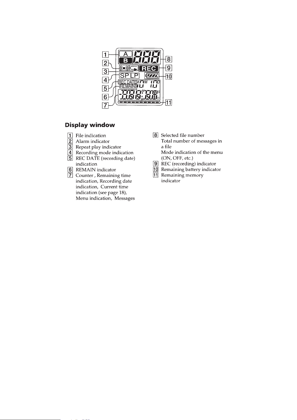
Sony ICD-00 Service Manual
ICD-R100
SERVICE MANUAL
Ver 1.0 1999.03
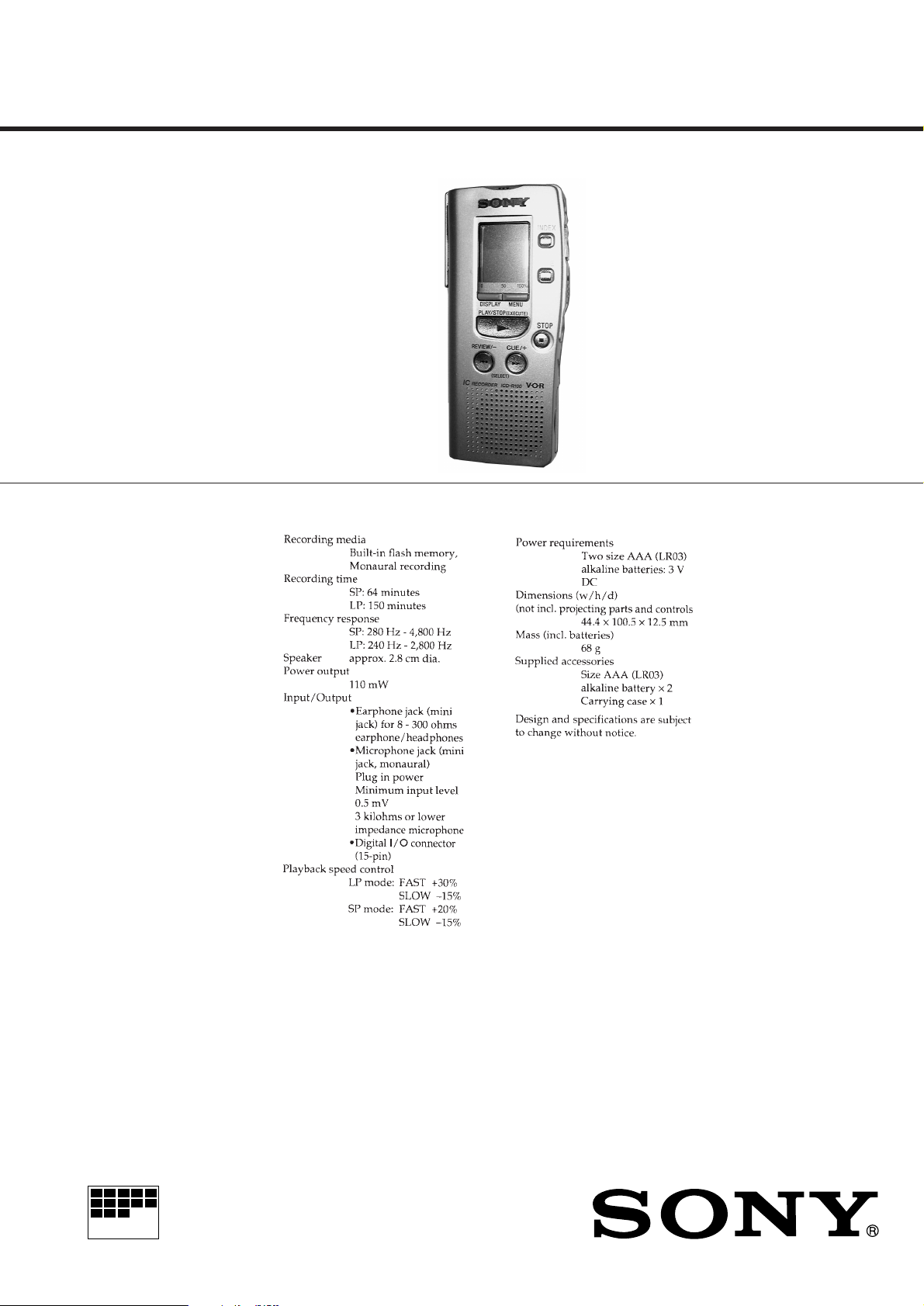
SPECIFICATIONS
Tourist Model
MICROFILM
IC RECORDER
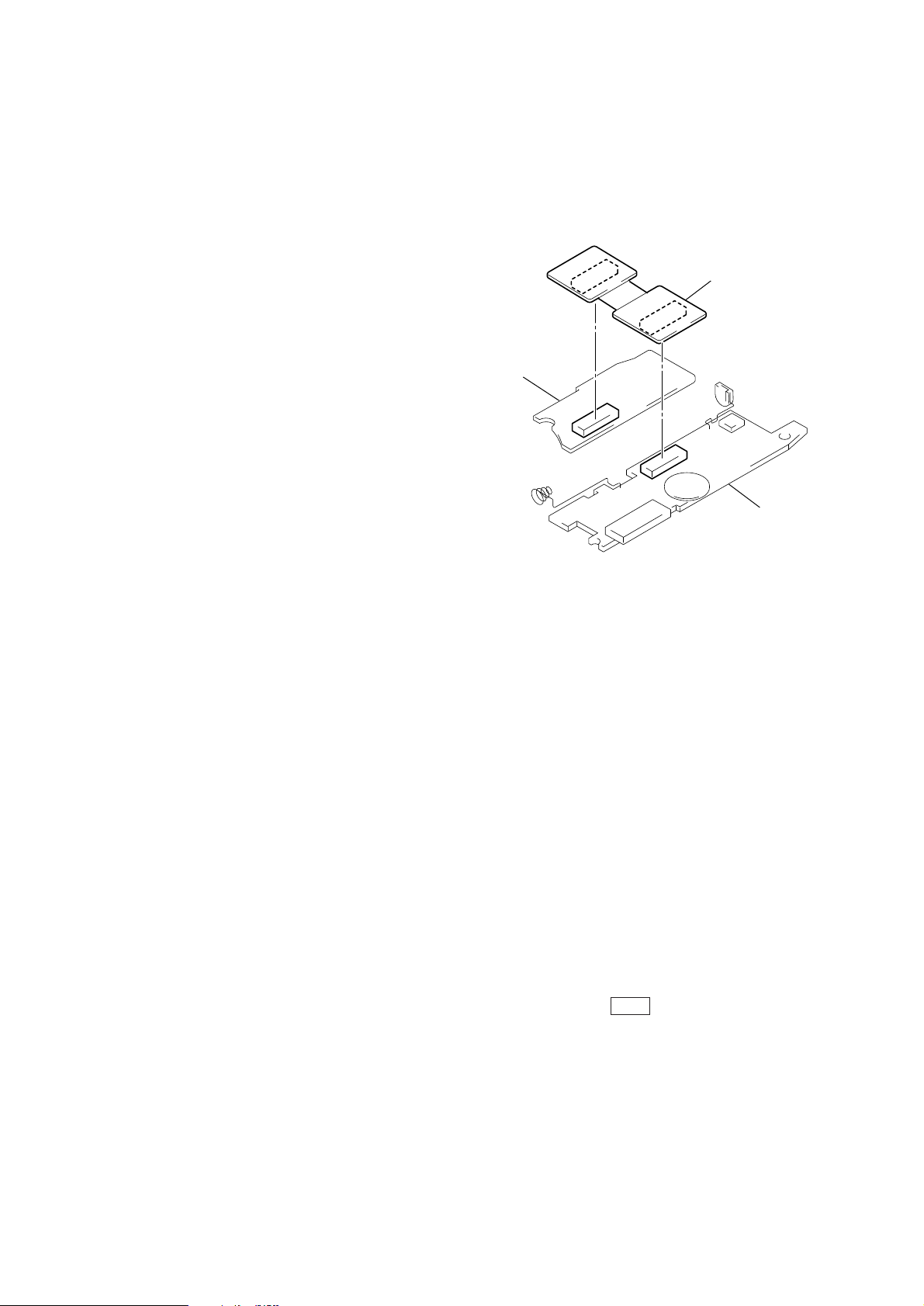
TABLE OF CONTENTS
d
Specifications ........................................................................... 1
1. SERVICING NOTE....................................................... 2
2. GENERAL ....................................................................... 3
SECTION 1
SERVICING NOTE
Using the special connector jig (J-2503-101-A) to connect the main
board and digital board will prove convenient when servicing the
unit with power applied.
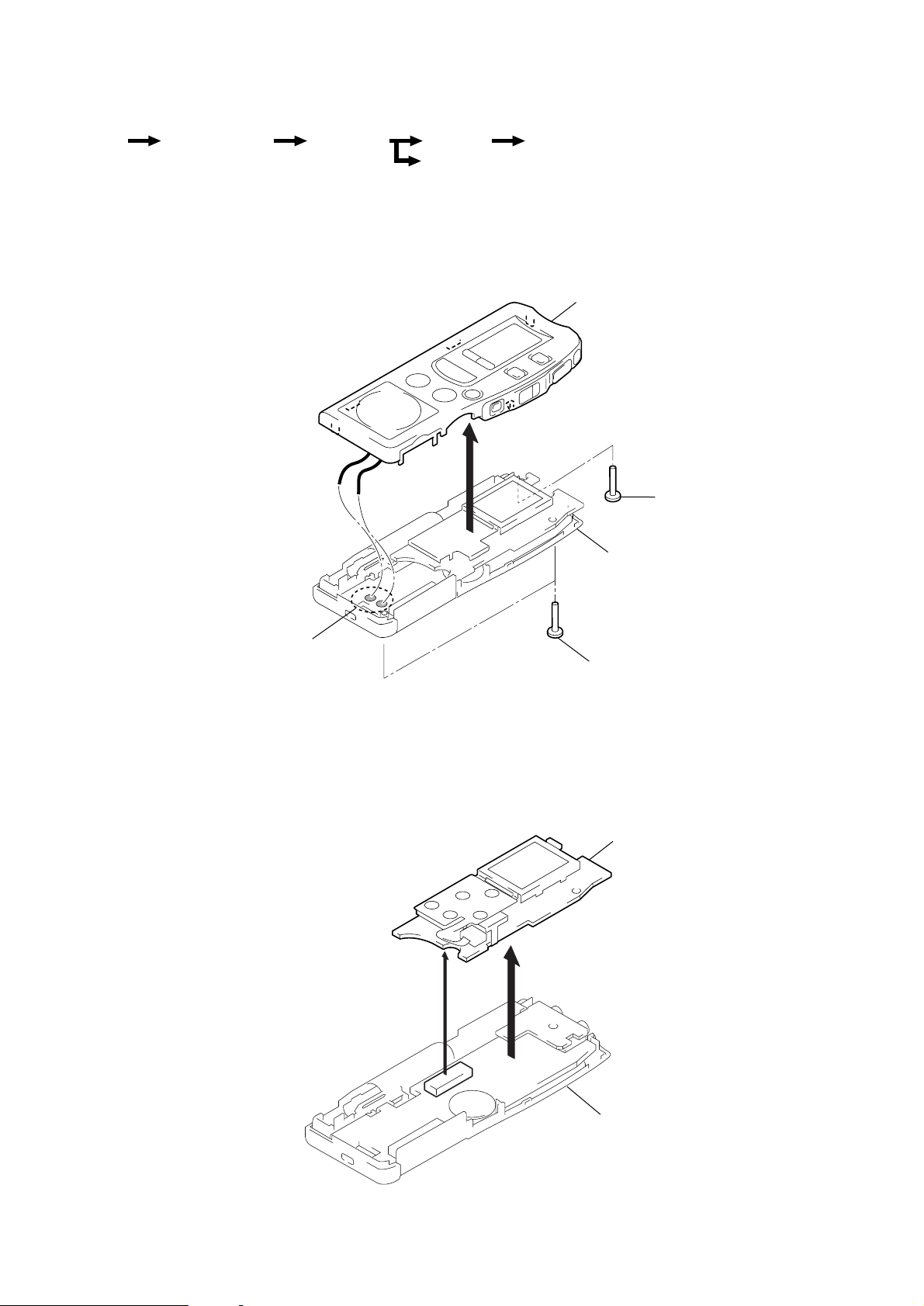
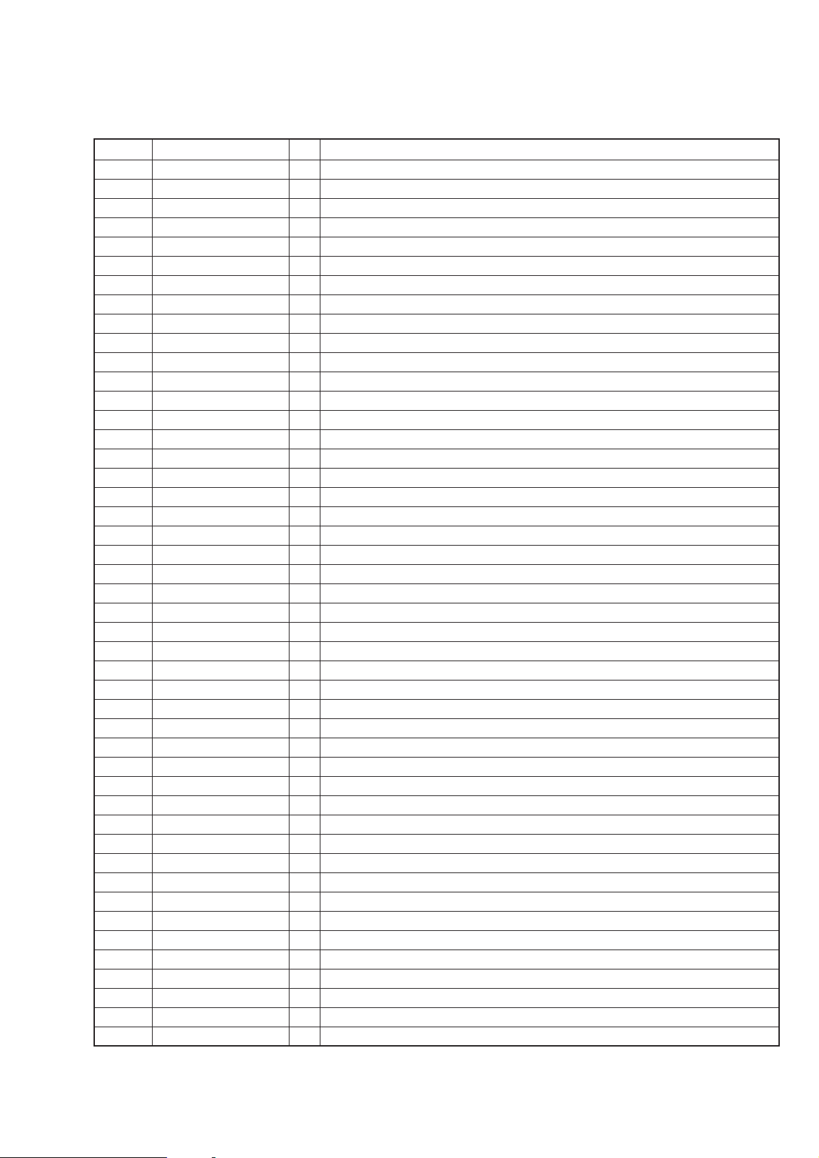
3. DISASSEMBLY
3-1. Lid ASSY, Upper ........................................................ 5
3-2. Digital Board .............................................................. 5
3-3. Switch Unit ................................................................. 6
3-4. Jack Board .................................................................. 6
3-5. Main Board ................................................................. 6
4. DIAGRAMS
4-1. Explanation of IC Terminals....................................... 7
4-2. Block Diagrams .......................................................... 9
4-3. Printed Wiring Boards (Main Section) ......................11
4-4. Schematic Diagram (Main Section) ......................... 13
4-5. Printed Wiring Boards (Digital Section) .................. 17
4-6. Schematic Diagram (Digital Section)....................... 18
5. EXPLODED VIEW...................................................... 23
6. ELECTRICAL PARTS LIST....................................24
Flexible Circuit Board Repairing
• Keep the temperature of the soldering iron around 270°C during
repairing.
• Do not touch the soldering iron on the same conductor of the
circuit board (within 3 times).
• Be careful not to apply force on the conductor when soldering or
unsoldering.
Notes on chip component replacement
• Never reuse a disconnected chip component.
• Notice that the minus side of a tantalum capacitor may be damaged by heat.
Jig (J-2503-010-A)
Digital board
Main boar
Note : Do not apply excessive amounts of flux during replace-
ment of electronic components since this may cause electrical shorts due to moisture.
Wipe off flux after electronic components exchange.
CAUTION ON REPLACING FLASH MEMORY
The BAD-BLOCK check* must be executed, when the flash
memory (IC701) in this set was replaced.
The set will not operation normally, unless this check is finished.
* The BAD-BLOCK check detects an area (bad-block) in the flash
memory where data validity cannot be guaranteed, and saves
this information in the TOC-AREA so that a bad-block is not
used.
BAD-BLOCK check procedure :
1. Apply 3V from regulated power supply to the battery
terminals.
2. Once the power is supplied, the check starts and then
proceeds for approx. 3 minutes. (Be sure to keep applying
the power during the check)
3. When the check completes, the result is shown as bellows.
OK: Only the LCD back light LED (D503, 504) turns on.
NG: Red LED blinks or turns on or green LED turns on in
the OPR LED (D502),
4. In case of OK, press the STOP button.
Note :
• In case of NG, check system control IC (IC704), flash memory
IC (IC701) and the peripheral circuit. (Particularly, check carefully the soldering of the flash memory)
• After finishing the BAD-BLOCK check, assemble the set, load
the dry battery, and confirm if the set operates normally.
– 2 –
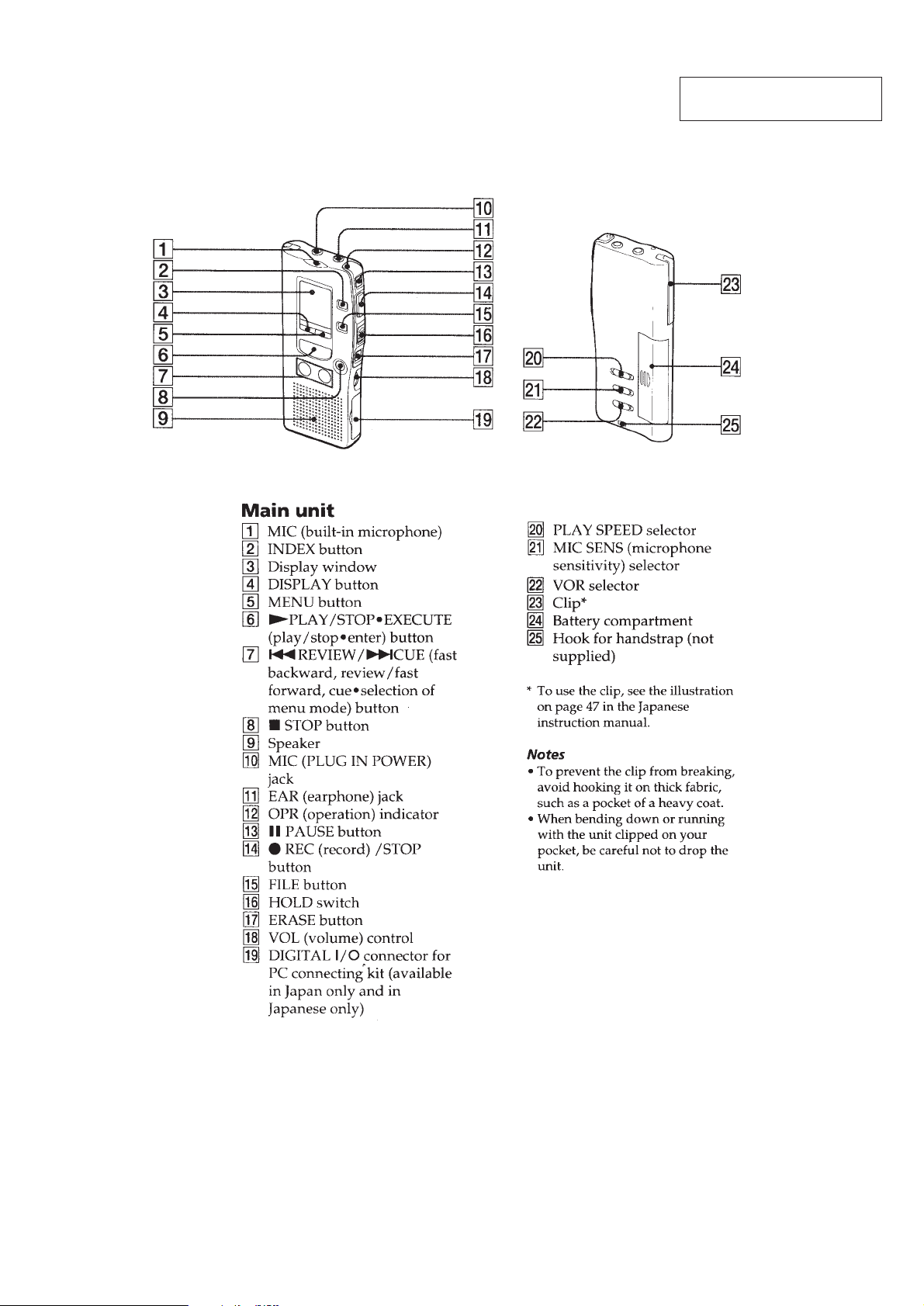
LOCATION AND FUNCTION OF CONTROLS
SECTION 2
GENERAL
This section is extracted from
instruction manual.
– 3 –
– 4 –
SECTION 3
)
DISASSEMBLY
r
The equipment can be removed using the following procedure.
Set
Note : Follow the disassembly procedure in the numerical order given.
3-1. LID ASSY, UPPER
Lid ASSY, Upper
Digital board Jack board Main board
Switch unit
4
Lid ASSY, Upper
1
Screw (B1.7X10
3
Remover solder
3-2. DIGITAL BOARD
2
Case
2
Screws (B1.7X9)
Note : Not using a screw (10mm) of step
1 for this place.
Digital board
Remove the
1
connector
(CN703)
– 5 –
Case
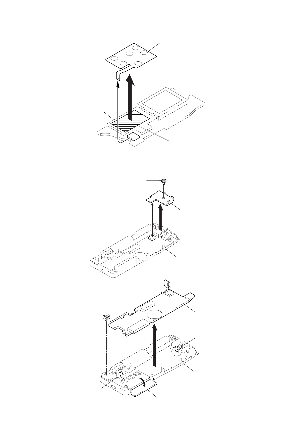
d
d
3-3. SWITCH UNIT
3-4. JACK BOARD
Digital board
1
1
Screw (B1.7X4)
Switch unit
2
Double sided adhesive tape
Note : The switch unit is secured with double-sided
tape.
When removed the switch unit, change it for
a new component.
3-5. MAIN BOARD
2
Remove the
connector
(CN102)
4
3
Jack boar
Case
Main boar
2
Claw
3
1
Case
Claw
Cap (PC)
– 6 –
SECTION 4
DIAGRAMS
4-1. EXPLANATION OF IC TERMINALS
IC704 µPD780308GC-113-8EU (SYSTEM CONTROL)
Pin No. Pin name I/O Description
1 KEY0 I Key input
2 KEY1 I Key input
3 SPDSW I Playback speed switch input.
4 XHOLD I Hold switch input.
5 HPMUTE O Earphone mute output.
6 PCLE O PC link permission signal output.
7 XFMCE O CE output for flash memory.
8 VDDO – Power supply terminal.
9 AVREF I A/D reference voltage input.
10 XFMWE O Write enable signal output for flash memory.
11 XFMALE O ALE signal output.
12 VSS1 – Ground.
13 XFMR/B I Flash memory Ready/Busy signal input.
14 XFMCLE O CLE signal output for flash memory.
15 SYNCOUT O SYNC signal output.
16 SYNCMSK O SYNC output control signal output.
17 XFMRE O Flash memory read enable signal output.
18 MSKCLK I SYNC output control clock input.
19 XFMWP O Flash memory WP signal output.
20 XFMSE O Flash memory SE signal output.
21 BEEP O BEEP signal output (2.4kHz).
22 LIGHT O LCD back lignt control output.
23 – 26 COMO 0–3 O LCD common signal output.
27 BIAS – Connect to VCC (LCD BIAS).
28 – 30 VLC 0 – 2 – LCD drive power supply.
31 VSS0 – Ground.
32 – 61 S0 – S29 O LCD segment signal output.
62 XVORSW I VOR switch input.
63 XVORIN I VOR signal input.
64 XTEST I Test terminal.
65 XDSPDEN O DSP registor control I/F enable signal output.
66 LEDREC O REC LED (red) ON/OFF output.
67 LEDPB O PLAY LED (green) ON/OFF output.
68 AMPPOW O Power down control output for IC108.
69 SPOWER O IC101 and analog power supply control output.
70 RTCCE O Real time colck CE signal output.
71 XPDRST O Reset signal output for IC101.
72 DSPIS I Serial data input from IC101.
73 DSPIR O Playback serial data output for IC101.
74 XBLCK O DSP bit clock signal output.
75 RTCDI I Real time colck data input.
76 RTCDO O RTC data and DSP registor contrl data output.
77 RTCCLK O RTC I/F data and DSP registor control clock output.
78 IC – Ground.
79 X2 O System clock output (5MHz).
80 X1 I System clock input (5MHz).
– 7 –
Pin No. Pin name I/O Description
81 VDD1 – Power supply terminal.
82 XT1 I Sub clock input.
83 XT2 I Sub clock turn over input.
84 XRESET I Reset signal input.
85 PCLINK I PC link connection detect input.
86 WAKEUP I WAKE UP signal input.
87 RTCINT I Real time clock (2Hz) signal input.
88 FLMPOW O Flash memory and IC707 power ON/OFF.
89 LPMODE O LPF switch control output.
90 LMUTE O Line mute ON/OFF signal output.
91 – 98 FMIO 0 – 7 I/O Data bus.
99 AVSS – A/D converter ground.
100 BATT I Power supply voltage detect input.
– 8 –
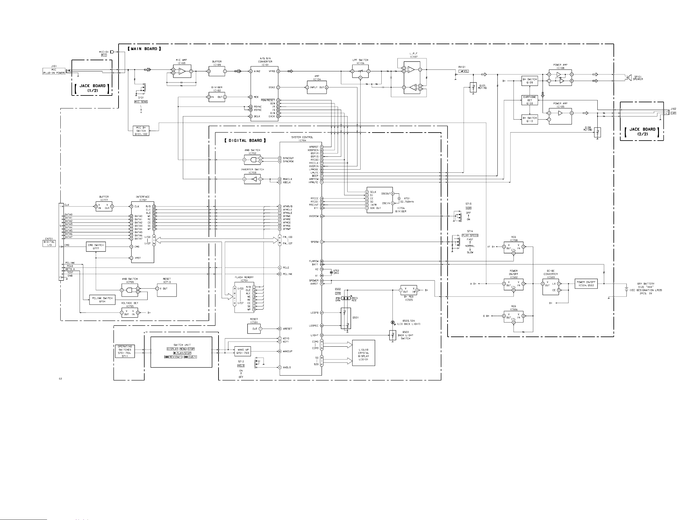
4-2. BLOCK DIAGRAMS
ICD-R100
– 9 – – 10 –
• Signal path.
F : PLAY
L : REC
ICD-R100
r
Semiconductor
Location
Ref. No. Location
D501 F-5
IC101 C-6
IC102 C-5
IC103 B-2
IC104 C-2
IC105 D-2
IC106 C-6
IC107 D-6
IC108 G-2
IC109 B-6
IC502 G-5
IC503 E-5
IC504 B-5
IC506 H-5
IC705 F-6
IC707 E-2
IC708 E-2
IC709 D-3
IC710 C-2
IC777 D-6
Q101 G-5
Q102 H-5
Q103 B-3
Q105 F-2
Q108 B-5
Q109 F-2
Q110 D-2
Q502 B-3
Q704 D-3
Q777 D-2
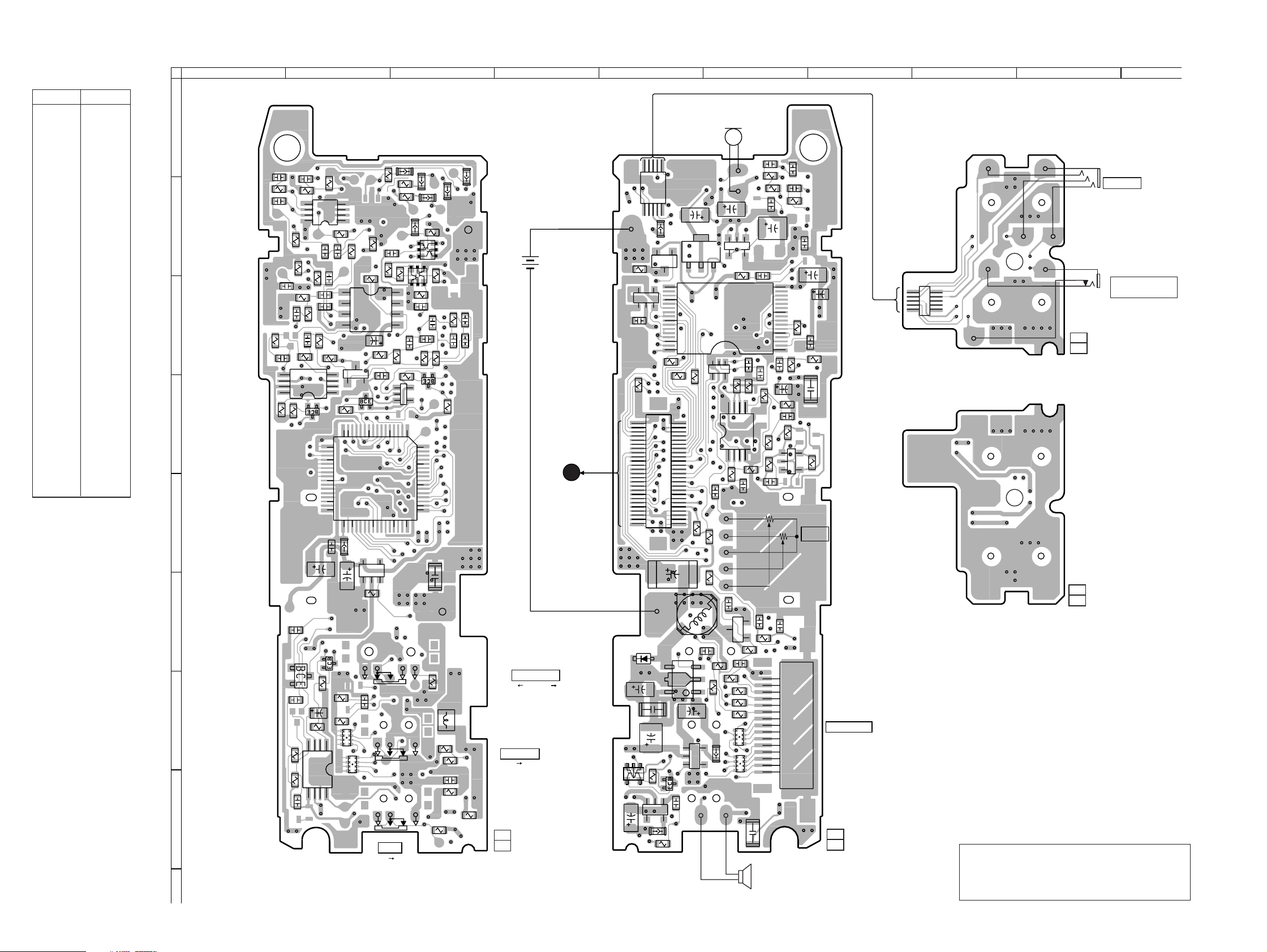
4-3. PRINTED WIRING BOARDS (MAIN SECTION)
1 2 3 4 5 6 7 8 910
A
[MAIN BOARD]
(SIDE A)
FB102
B
C
C162
D
E
F
G
H
C148
R110
C108
R139
5
8
C112
R132
R137
02
R164
R121
C125
C131
Q105
C155
R153
R154
C161
C105
R134
5
8
R142
R118
C156
R138
IC105
Q110
R152
4
IC108
5
IC103
R167
C157
R131
17
20
25
30
32
C718
C149
R163
R751
C717
1
8
C126
C127
4
R151
R758
R756
R135
C116
1
IC710
4
1
1
R765
16
33
C722
Q109
RB704
RB705
4
1
C109
C128
35
R111
R133
TP112
IC104
3
Q777
FB701
5
IC708
1
C723
R122
C725
2
10
IC707
40
R732
S714
R102
R157
R166
4
3
S101
OFF ON
C114
R509
1
3
5
45
S713
VOR
R156
R510
8
5
R749
IC709
48
FB104
R143
1
50
FB106
FB105
C139
C140
R144
5
Q704
4
1-673-293-
Q502
R504
R506
C506
64
60
55
49
R105
R724
R140
Q103
C144
R146
R727
R104
FB107
C143
C508
R145
R750
L503
C102
R103
C142
C145
R514
FB101
(IEC DESIGNATION LR03)
SLOW NORMAL FAST
MIC SENS
11
(11)
DRY BATTERY
SIZE "AAA"
2PCS, 3V
S714
PLAY SPEED
S101
L H
[MAIN BOARD]
(SIDE B)
A
DIGITAL BOARD
CN705
Q101
C510
26
30
35
40
45
50
C513
R515
C110
C512
15
FB103
54
IC102
123
R113
R764
CN703
D501
C505
R107
IC506
45
610
IC504
IC503
4
5
3
17
20
25
30
32
15
10
L501
123
CN102
12
R116
C509
C502
Q102
FB503
R725
C137
Q108
GDS
IC106
R117
25
20
5
1
IC502
1
2
3
C716
45
C130
R511
C710
3
2
1
IC101
R171
R726
R743
5
4
MIC101
MIC
C101
45
IC109
R120
123
8
1
R512
R155
C719
IC705
R755
R752
FB501
R136
IC107
C129
2
3
1
RB702
RB701
C104
R106
C158
123
C133
5
4
R147
R754
R108
R733
C724
15
10
R160
R753
R141
R763
5
1
SPEAKER
C160
C118
16
C152
C141
C134
R149
R762
R148
1
2
34
IC777
C730
C153
1-673-293-
C151
SP101
C147
10
5
1
C107
R161
R150
C146
C154
C103
R109
C111
R112
5
RV101
∑VOL
CN701
C124
C106
C136
R761
R162
CN701
DIGITAL I/O
11
(11)
CN101
5
1
[JACK BOARD] (SIDE A)
J102
EAR
6
(PLUG-IN POWER)
10
1-673-294-
11
(11)
[JACK BOARD] (SIDE B)
1-673-294-
Note:
• X : parts extracted from the component side.
®
•
: Through hole.
• b : Pattern from the side which enables seeing.
(The other layers' patterns are not indicated.)
Caution:
Pattern face side: Parts on the pattern face side seen from the
(Side B) pattern face are indicated.
Parts face side: Parts on the parts face side seen from the
(Side A) parts face are indicated.
11
(11)
J101
MIC
– 11 – – 12 –
4-4. SCHEMATIC DIAGRAM (MAIN SECTION)
p
r
Refer to page 21 for IC Block Diagrams.
r
Wavef orms
1
ICD-R100
4.1 Vp-p
91.4 kHz
IC503 4
VOLT/DIV : 1 V AC
TIME/DIV : 2 µsec
2
3.5 Vp-p
REC 11 kHz
PLAY 13 kHz
IC102 3
VOLT/DIV : 1 V AC
TIME/DIV : 20 µsec
3
1.7 Vp-
14kHz
IC102 4
Note:
• All capacitors are in µF unless otherwise noted. pF: µµF
50 WV or less are not indicated except for electrolytics
and tantalums.
• All resistors are in Ω and 1/
specified.
• U : B+ Line.
• Power voltage is dc 3V and fed with regulated dc power
supply from battery terminal.
• Voltages and waveforms are dc with respect to ground
under no-signal conditions.
no mark : REC
( ) : PLAY
• Voltages and current are taken with a VOM (Input impedance 10 MΩ).
Voltage variations may be noted due to normal production tolerances.
• Waveforms are taken with a oscilloscope.
Voltage variations may be noted due to normal production tolerances.
• Circled numbers refer to waveforms.
• Signal path.
F : PLAY
L : REC
VOLT/DIV : 5 V AC
TIME/DIV : 20 µsec
4
W or less unless otherwise
– 13 – – 14 – – 16 –– 15 –
ICD-R100
p
p
4-5. PRINTED WIRING BOARDS (DIGITAL SECTION)
1 2 3 4 5 6
[DIGITAL BOARD] (SIDE A)
5
R505
FB702
R766
R507
1
2
Q503
IC505
R508
CN702
15
25
1510152024
R737
R744
D701
R701
R728
R719
SWITCH UNIT
DISPLAY MENU STOP
”PLAY/STOP
=REVIEW/– +CUE/+
A
R711
R712
D503
R715
D504
LCD BACK LIGHT
B
LCD101
LIQUID CRYSTAL DISPLAY
C
D
R702
IC701
E
25 30 35 40 45 48
IC703
13
R713
2
3
1
4
2
F
45
IC702
Q703
R714
G
02
Q501
R722
BP701
R747
C709
1
3
1
5
10
20
30
C715
34
CN704
1-673-292-
D502
OPR
D502
S702
R721
6
R513
S703
R731
R729
R503
R720
11
(11)
S711
P PAUSE
S703
INDEX
S702
FILE
S712
HOLD
ON
OFF
ERASE
[DIGITAL BOARD] (SIDE B)
S711
S701
IC501
S712
R734
S704
S704
JC701
R730
rREC/STOP
C504
R501
R502
C727
51
55
60
C501
65
70
75
JC702
R739
S701
76 80 85 90
X702
IC706
5
X701
6
C708
C701
1
10
C704
C702
1-673-292-
C726
R740
R741
Q701
IC704
C711
R742
R738
15
95
FB703
CN705
25
20
10
5
1
C712
26
30
35
40
45
50
Q702
100
R703
R704
263035404550
R723
C721
20
10
25
15
5
1
R745
A
11
(11)
r
Semiconductor
Location
Ref. No. Location
D502 A-3
D503 B-1
D504 B-2
D701 E-2
IC501 C-4
IC505 A-2
IC701 E-2
IC702 F-1
IC703 F-2
IC704 C-5
IC706 E-5
Q501 A-2
Q503 A-2
Q701 F-5
Q702 F-6
Q703 F-1
MAIN BOARD
CN703
Note on Printed Wiring Boards:
Note:
• X : parts extracted from the component side.
¢
•
•
• b : Pattern from the side which enables seeing.
(The other layers' patterns are not indicated.)
Caution:
Pattern face side: Parts on the pattern face side seen from the
(Side B) pattern face are indicated.
Parts face side: Parts on the parts face side seen from the
(Side A) parts face are indicated.
: internal component.
®
: Through hole.
4-6. SCHEMATIC DIAGRAM (DIGITAL SECTION)
r
Refer to page 22 for IC Block Diagrams.
r
Wavef orms
1
IC704 &ª
2
IC706 8
1.3 Vp-
5 MHz
VOLT/DIV : 0.5 V AC
TIME/DIV : 50 nsec
438 mVp-
32.768 kHz
VOLT/DIV : 0.1 V AC
TIME/DIV : 10 µsec
4
REC 11 kHz
PLAY 13 kHz
IC704 !§
5
32.768 kHz
IC704 *™
3
3.5 Vp-p
REC 11 kHz
PLAY 13 kHz
IC704 !∞
Note:
• All capacitors are in µF unless otherwise noted. pF: µµF
50 WV or less are not indicated except for electrolytics
and tantalums.
• All resistors are in Ω and 1/
specified.
¢
•
• U : B+ Line.
• Power voltage is dc 3V and fed with regulated dc power
• Voltages and waveforms are dc with respect to ground
• Voltages and current are taken with a V OM (Input imped-
• Waveforms are taken with a oscilloscope.
• Circled numbers refer to waveforms.
: internal component.
supply from battery terminal.
under no-signal conditions.
no mark : REC
( ) : PLAY
ance 10 MΩ).
Voltage variations may be noted due to normal production tolerances.
Voltage variations may be noted due to normal production tolerances.
VOLT/DIV : 1 V AC
TIME/DIV : 20 µsec
4
W or less unless otherwise
3.5 Vp-p
VOLT/DIV : 1 V AC
TIME/DIV : 20 µsec
0.8 Vp-p
VOLT/DIV : 0.2 V AC
TIME/DIV : 10 µsec
– 19 – – 20 –– 17 – – 18 –
 Loading...