

Page 1

HT-RT3
SA-WRT3
SERVICE MANUAL
Ver. 1.5 2017.09
• All the units included in the HT-RT3 (SA-WR T3,
SS-RT3/SRT3, remote control) are required to
confi rm the operation of SA-WRT3. Check in
advance that you have all the units.
Note:
Be sure to keep your PC used for service and
checking of this unit always updated with the
latest version of your anti-virus software.
In case a virus affected unit was found during
service, contact your Service Headquarters.
COMPONENT MODEL NAME
HT-RT3
Bar Speaker (Speaker System) SS-RT3
Surround Speaker (Speaker System) SS-SRT3
Subwoofer (Active Subwoofer) SA-WRT3
• The service manual for SS-RT3/SRT3 has been issued separately.
Please refer to the service manual for information.
US Model
Canadian Model
AEP Model
UK Model
E Model
Australian Model
SPECIFICATIONS
Amplifi er section
US models:
POWER OUTPUT AND TOTAL
HARMONIC DISTORTION:
(FTC)
Front L + Front R:
With 2.5 ohms loads, both channels
driven, from 200 Hz – 20,000 Hz;
rated
RMS
POWER OUTPUT (reference):
Front L/Front R/Surround L/
Surround R:
65 W (per channel at 2.5 ohms,
1 kHz)
Center:
170 W (at 4 ohms, 1 kHz)
Subwoofer:
170 W (at 4 ohms, 1 kHz)
Except US models:
POWER OUTPUT (rated)
Front L + Front R:
35 W + 35 W (at 2.5 ohms, 1 kHz,
1% THD)
POWER OUTPUT (reference)
Front L/Front R/Surround L/
Surround R:
65 W (per channel at 2.5 ohms,
1 kHz)
Center:
170 W (at 4 ohms, 1 kHz)
Subwoofer:
170 W (at 4 ohms, 1 kHz)
Inputs
USB
ANALOG IN
TV IN (OPTICAL)
Output
HDMI OUT (ARC)
30 watts per channel minimum
power, with no more than
UFOELK - 2/21/2018 5:23 PM
1% total harmonic distortion from
250 milliwatts to rated output.
HDMI section
Connector
Type A (19pin)
USB section
(USB) port
Type A
BLUETOOTH section
Communication system
BLUETOOTH Specifi cation
version 4.2
Output
BLUETOOTH Specifi cation
Power Class 1
Maximum communication range
Line of sight approx. 25 m (82 ft)
Frequency band
2.4 GHz band (2.4000 GHz –
2.4835 GHz)
Modulation method
FHSS (Freq Hopping Spread
Spectrum)
Compatible BLUETOOTH profi les
A2DP 1.2 (Advanced Audio
Distribution Profi le)
AVRCP 1.6 (Audio Video Remote
Control Profi le)
Supported Codecs
SBC4), AAC
Transmission range (A2DP)
20 Hz – 20,000 Hz (Sampling
frequency 32 kHz, 44.1 kHz,
48 kHz)
1)
The actual range will vary depending
on factors such as obstacles between
devices, magnetic fi elds around a
microwave oven, static electricity,
cordless phone, reception sensitivity,
antenna’s performance, operating
system, software application, etc.
3)
5)
2)
3)
4)
5)
Speaker section
Speaker system
Subwoofer system, Bass refl ex
Speaker
160 mm (6
General
1)
Power requirements
LA9 models only:
110 V - 240 V AC, 50/60 Hz
US, CND models only:
120 V AC, 60 Hz
EA models only:
127 V – 240 V AC, 50/60 Hz
2)
Except LA9, US, CND, EA
models:
220 V – 240 V AC, 50/60 Hz
Power consumption
On: 85 W
Standby: 0.5 W or less (Power
(When “CTRL” in “HDMI>” and
Standby: 2.8 W or less
BLUETOOTH standard profi les
indicate the purpose of BLUETOOTH
communication between devices.
Codec: Audio signal compression and
conversion format
Subband Codec
Advanced Audio Coding
3
/8 in) cone type
saving mode)
“BTSTB” in “BT >” are set to
“OFF”)
6)
HOME THEATRE SYSTEM
(When “CTRL” in “HDMI>”
or “BTSTB” in “BT >” is set to
“ON”)
Dimensions (w/h/d) (approx.)
190 mm × 392 mm × 315 mm
1
/2 in × 15 1/2 in × 12 1/2 in)
(7
Mass (approx.)
7.8 kg (17 Ib 4 oz)
6)
The system will automatically enter
Power saving mode when there is
no HDMI connection and no BLUETOOTH pairing history, regardless
of the settings you have made for
“CTRL” in “HDMI>” and “BTSTB”
in “BT >”.
Supplied accessories
Remote control (1)
R03 (size AAA) batteries (2)
High Speed HDMI cable (1) (E12, LA9,
AR, AUS, SP, EA)
Optical digital cable (1) (US, CND,
AEP, UK)
AC plug adaptor (1) (LA9)
Design and specifi cations are subject to
change without notice.
HT-RT3
SA-WRT3
9-890-680-06
2017I33-1
2017.09
©
ACTIVE SUBWOOFER
Sony Video & Sound Products Inc.
Page 2

HT-RT3
Ver. 1.1
Copyrights and Trademarks
• This system incorporates Dolby* Digital.
* Manufactured under license from Dolby Laboratories.
Dolby and the double-D symbol are trademarks of Dolby Laboratories.
• The BLUETOOTH
Bluetooth SIG, Inc. and any use of such marks by Sony Corporation is under
license. Other trademarks and trade names are those of their respective owners.
• This system incorporates High-Defi nition Multimedia Interface (HDMI™)
technology.
The terms HDMI and HDMI High-Defi nition Multimedia Interface, and the
HDMI Logo are trademarks or registered trademarks of HDMI Licensing LLC
in the United States and other countries.
• The N-Mark is a trademark or registered trademark of NFC Forum, Inc. in the
United States and in other countries.
• Android™ is a trademark of Google Inc.
• Google Play™ is a trademark of Google Inc.
• MPEG Layer-3 audio coding technology and patents licensed from Fraunhofer
IIS and Thomson.
• Windows Media is either a registered trademark or trademark of Microsoft
Corporation in the United States and/or other countries.
• This product is protected by certain intellectual property rights of Microsoft
Corporation. Use or distribution of such technology outside of this product is
prohibited without a license from Microsoft or an authorized Microsoft subsidiary.
• “BRAVIA” is a trademark of Sony Corporation.
• “ClearAudio+” is a trademark of Sony Corporation.
• “PlayStation” is a registered trademark of Sony Computer Entertainment Inc.
• Apple, the Apple logo, iPhone, iPod, iPod touch, and Retina are trademarks of
Apple Inc., registered in the U.S. and other countries. App Store is a service
mark of Apple Inc.
“Made for iPod,” and “Made for iPhone” mean that an electronic
accessory has been designed to connect specifi cally to iPod or iPhone, respectively,
and has been certifi ed by the developer to meet Apple performance standards. Apple
is not responsible for the operation of this device or its compliance with safety and
regulatory standards. Please note that the use of this accessory with iPod or iPhone
may affect wireless performance.
®
word mark and logos are registered trademarks owned by
Compatible iPod/iPhone models
The compatible iPod/iPhone models are as follows. Update your iPod/iPhone with
the latest software before using with the system. BLUETOOTH technology works
with:
- iPhone 6s Plus/iPhone 6s/iPhone 6 Plus/iPhone 6/iPhone 5s/iPhone 5c/iPhone 5
- iPod touch (6th generation)/iPod touch (5th generation)
• THIS PRODUCT IS LICENSED UNDER THE MPEG-4 VISUAL PATENT
PORTFOLIO LICENSE FOR THE PERSONAL AND NON-COMMERCIAL
USE OF A CONSUMER FOR
(i) ENCODING VIDEO IN COMPLIANCE WITH THE MPEG-4 VISUAL
STANDARD (“MPEG-4 VIDEO”)
AND/OR
(ii) DECODING MPEG-4 VIDEO THAT WAS ENCODED BY A CONSUMER
ENGAGED IN A PERSONAL AND NON-COMMERCIAL ACTIVITY AND/
OR WAS OBTAINED FROM A VIDEO PROVIDER LICENSED TO PROVIDE MPEG-4 VIDEO.
NO LICENSE IS GRANTED OR SHALL BE IMPLIED FOR ANY OTHER USE.
ADDITIONAL INFORMATION INCLUDING THAT RELATING TO PROMOTIONAL, INTERNAL AND COMMERCIAL USES AND LICENSING MAY BE
OBTAINED FROM MPEG LA, L.L.C.
HTTP://WWW.MPEGLA.COM
• All other trademarks are trademarks of their respective owners.
• Other system and product names are generally trademarks or registered trademarks of the manufacturers. ™ and ® marks are not indicated in this document.
• Abbreviation
AR : Argentina model
AUS : Australian model
CND : Canadian model
E12 : 220-240 V AC area in E model
EA : Saudi Arabia model
LA9 : Latin-American model
SP : Singapore model
2
Page 3
NOTES ON CHIP COMPONENT REPLACEMENT
• Never reuse a disconnected chip component.
• Notice that the minus side of a tantalum capacitor may be damaged by heat.
SAFETY CHECK-OUT
After correcting the original service problem, perform the following safety check before releasing the set to the customer:
Check the antenna terminals, metal trim, “metallized” knobs,
screws, and all other exposed metal parts for AC leakage.
Check leakage as described below.
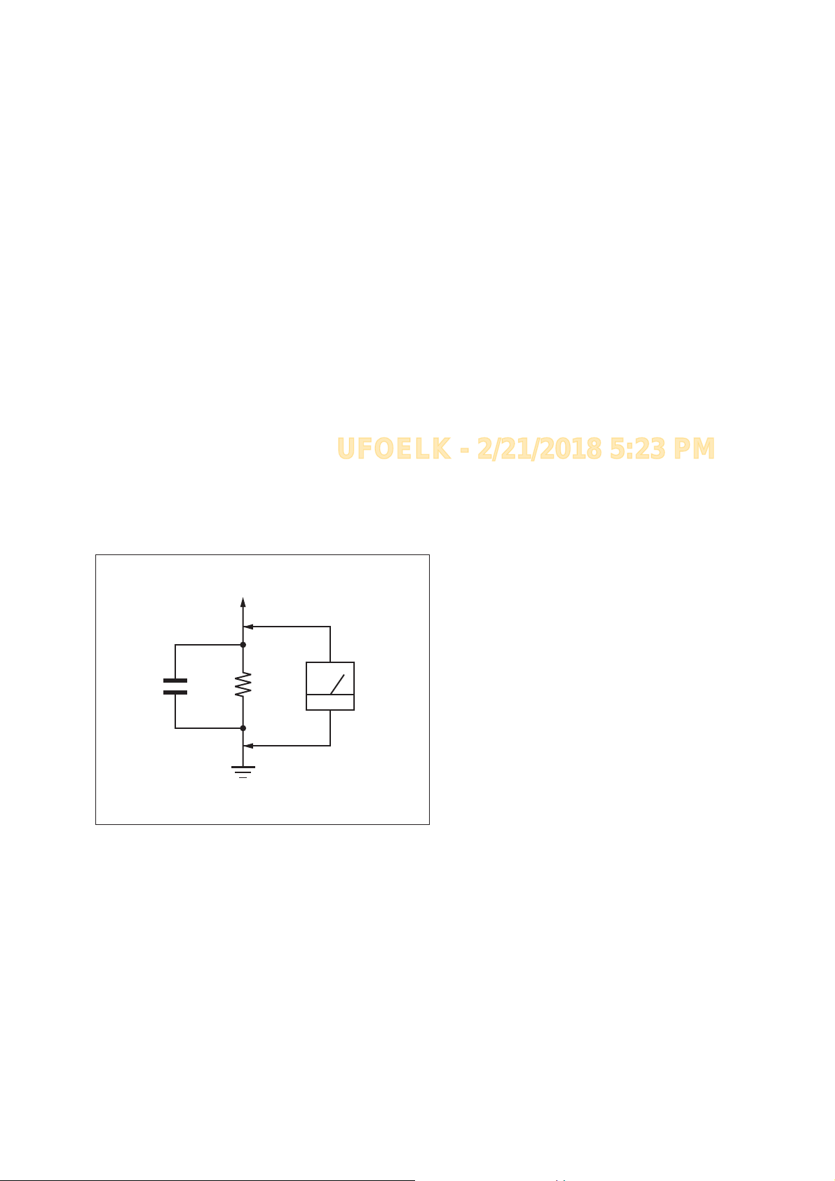
LEAKAGE TEST
The AC leakage from any exposed metal part to earth ground and
from all exposed metal parts to any exposed metal part having a
return to chassis, must not exceed 0.5 mA (500 microamperes).
Leakage current can be measured by any one of three methods.
1. A commercial leakage tester, such as the Simpson 229 or RCA
WT-540A. Follow the manufacturers’ instructions to use these
instruments.
2. A battery-operated AC milliammeter. The Data Precision 245
digital multimeter is suitable for this job.
3. Measuring the voltage drop across a resistor by means of a
VOM or battery-operated AC voltmeter . The “limit” indication
UFOELK - 2/21/2018 5:23 PM
is 0.75 V, so analog meters must have an accurate low-voltage
scale. The Simpson 250 and Sanwa SH-63Trd are examples
of a passive VOM that is suitable. Nearly all battery operated
digital multimeters that have a 2V AC range are suitable. (See
Fig. A)
HT-RT3
To Exposed Metal
Parts on Set
AC
1.5 kΩ0.15 μF
Earth Ground
voltmeter
(0.75 V)
Fig. A. Using an AC voltmeter to check AC leakage.
SAFETY-RELATED COMPONENT WARNING!
COMPONENTS IDENTIFIED BY MARK 0 OR DOTTED LINE
WITH MARK 0 ON THE SCHEMATIC DIAGRAMS AND IN
THE PARTS LIST ARE CRITICAL TO SAFE OPERATION.
REPLACE THESE COMPONENTS WITH SONY PARTS
WHOSE PART NUMBERS APPEAR AS SHOWN IN THIS
MANUAL OR IN SUPPLEMENTS PUBLISHED BY SONY.
ATTENTION AU COMPOSANT AYANT RAPPORT
À LA SÉCURITÉ!
LES COMPOSANTS IDENTIFIÉS PAR UNE MARQUE 0 SUR
LES DIAGRAMMES SCHÉMATIQUES ET LA LISTE DES
PIÈCES SONT CRITIQUES POUR LA SÉCURITÉ DE FONCTIONNEMENT. NE REMPLACER CES COMPOSANTS QUE
PAR DES PIÈCES SONY DONT LES NUMÉROS SONT DONNÉS DANS CE MANUEL OU DANS LES SUPPLÉMENTS
PUBLIÉS PAR SONY.
3
Page 4

HT-RT3
TABLE OF CONTENTS
1. SERVICING NOTES ............................................. 5
2. DISASSEMBLY
2-1. Disassembly Flow ........................................................... 8
2-2. Front Panel Section ......................................................... 9
2-3. Loudspeaker 16cm .......................................................... 10
2-4. Chassis Section ............................................................... 11
2-5. BLUETOOTH Module ................................................... 11
2-6. SPEAKER CHUKEI PC BOAR Board .......................... 12
2-7. MAIN Board, CONNECTOR Board,Switching
Regulator ........................................................................ 13
3. TEST MODE ............................................................ 14
4. TROUBLESHOOTING ........................................... 15
5. DIAGRAMS
5-1. Block Diagram - MAIN CONTROL Section - ............... 19
5-2. Block Diagram - AUDIO Section - ................................. 20
5-3. Block Diagram - POWER SUPPLY Section - ................ 21
5-4. Printed Wiring Boards - MAIN Board - ......................... 23
5-5. Printed Wiring Boards - OLED CHUKEI PC
BOAR Board - ................................................................ 24
5-6. Schematic Diagram - OLED CHUKEI PC
BOAR Board - ................................................................ 24
5-7. Printed Wiring Board - TOUCH Board - ........................ 25
5-8. Schematic Diagram - TOUCH Board - ........................... 25
5-9. Printed Wiring Board - SPEAKER CHUKEI PC
BOAR Board - ................................................................ 26
5-10. Schematic Diagram - SPEAKER CHUKEI PC
BOAR Board - ................................................................ 26
5-11. Printed Wiring Board - CONNECTOR Board - ............. 27
5-12. Schematic Diagram - CONNECTOR Board - ................ 27
5-13. Printed Wiring Board - USB Board - .............................. 27
6. EXPLODED VIEWS
6-1. Overall Section ............................................................... 30
6-2. Chassis Section ............................................................... 31
6-3. MAIN Board Section ...................................................... 32
7. ELECTRICAL PARTS LIST .............................. 33
Accessories are listed in the last part of the electrical parts list.
4
Page 5
SECTION 1
SERVICING NOTES
HT-RT3
Ver. 1.3
UNLEADED SOLDER
Boards requiring use of unleaded solder are printed with the leadfree mark (LF) indicating the solder contains no lead.
(Caution: Some printed circuit boards may not come printed with
the lead free mark due to their particular size)
: LEAD FREE MARK
Unleaded solder has the following characteristics.
• Unleaded solder melts at a temperature about 40 °C higher
than ordinary solder.
Ordinary soldering irons can be used but the iron tip has to be
applied to the solder joint for a slightly longer time.
Soldering irons using a temperature regulator should be set to
about 350 °C.
Caution: The printed pattern (copper foil) may peel away if
the heated tip is applied for too long, so be careful!
• Strong viscosity
Unleaded solder is more viscous (sticky, less prone to fl ow)
than ordinary solder so use caution not to let solder bridges
occur such as on IC pins, etc.
• Usable with ordinary solder
It is best to use only unleaded solder but unleaded solder may
also be added to ordinary solder.
ADVANCE PREPARATION WHEN CONFIRMING OPERATION
All the units included in the HT-RT3 (SA-WRT3, SS-RT3/SRT3,
remote control) are required to confi rm the operation of SA-WRT3.
Check in advance that you have all the units.
NOTE OF REPLACING THE IC1000 AND IC1002
ON THE MAIN BOARD AND THE COMPLETE MAIN
BOARD
When IC1000 and IC1002 on the MAIN board and the complete
MAIN board are replaced, it is necessary to spread the compound
between the MAIN board and the heat sink.
Spread the compound (THERMAL COMPOUND (G747)) referring to the fi gure below.
– MAIN Board (Component Side) –
NOTE OF PERFORMING THE OPERATION CHECK IN
THE STATE THAT HEAT SINK WAS REMOVED
When performing the operation check in the state that this unit was
disassembled, it is possible to perform the operation check in the
state that heat sink was removed. But don’t perform the operation
check in the long time, and perform the operation check in the
volume state as low as possible.
IF “PRTCT” APPEARS IN THE FRONT PANEL DISPLAY OF THE SUBWOOFER
t Press 1 to turn off the system. After
UFOELK - 2/21/2018 5:23 PM
the display turns off, disconnect the
AC power cord (mains lead) then
check that nothing is blocking the
ventilation holes of the Subwoofer.
thermal compound (G747)
IC1000
thermal compound (G747)
IC1002
NOTE OF REPLACING BLUETOOTH MODULE OR
RC-S730 (WW)
When the BLUETOOTH MODULE or RC-S730 (WW) is replaced, the MAC address for BLUETOOTH MODULE has been
changed. Please execute COLD RESET (refer to page 14) before
pairing with a Bluetooth device / NFC.
5
Page 6

HT-RT3
CAPACITOR ELECTRICAL DISCHARGE PROCESSING
When checking the board, for the electric shock prevention, connect the resistors to both ends of respective capacitor (C201 and
C207) to discharge the capacitor (C201 and C207).
- REGULATOR, SWITCHING 3L405W-2 Board
(EXCEPT E12) (Conductor Side) -
- REGULATOR, SWITCHING 3L405W-3 Board
(E12) (Conductor Side) -
C207
800 :/2 W
800 :/2 W
• Parts position
1. REGULATOR, SWITCHING 3L405W-2 board (Except
E12) (page 6)
2. REGULATOR, SWITCHING 3L405W-3 board (E12)
(page 6)
3. MAIN board (page 7)
1. REGULATOR, SWITCHING 3L405W-2 board (Except
E12)
– REGULATOR, SWITCHING 3L405W-2 Board
(EXCEPT E12) (Component Side) –
C402 T201
L401 C461 C215 C204
L101
TH101 RC201
C101
NR101
L102 C103
C102
C201
BOND FIXATION OF ELECTRIC PARTS
When REGULATOR, SWITCHING 3L405W-2 board (Except
E12), REGULATOR, SWITCHING 3L405W-3 board (E12) or
MAIN board is replaced, it is necessary to fi x parts to the boards
by using a specifi ed bond without fail.
• Object boards
1. REGULATOR, SWITCHING 3L405W-2 board (Except
E12)
2. REGULATOR, SWITCHING 3L405W-3 board (E12)
3. MAIN board
• Use bond
Part No. Description
7-600-020-70 ADHESIVE (SC608Z2) 180ML
C207 C211 T201R208C201
The portion which applies bond:
*
2. REGULATOR, SWITCHING 3L405W-3 board (E12)
– REGULATOR, SWITCHING 3L405W-3 Board
(E12) (Component Side) –
C402 T201 C101 C102
C215C461L401
L101
NR101
C103C204
RC201TH101
L102
C201 C207 C211 T201R208
The portion which applies bond:
*
6
Page 7

HT-RT3
Ver. 1.1
3. MAIN board
– MAIN Board (Component Side) –
CN3400
C1008
C1043
The portion which applies bond:
*
C1009
C1040
MODEL IDENTIFICATION
Distinguish by Part No. on the rear side of a main unit.
– Rear View –
MODEL NUMBER LABEL
MADE IN MALAYSIA
Destination Code
Part No.
UFOELK - 2/21/2018 5:23 PM
Model Part No.
US, CND
AEP
UK
AUS
E12
EA
SP
LA9
AR
• Abbreviation
AR : Argentina model
AUS : Australian model
CND : Canadian model
E12 : 220-240 V AC area in E model
EA : Saudi Arabia model
LA9 : Latin-American model
SP : Singapore model
4-586-817-0[]
4-586-817-1[]
4-586-817-2[]
4-586-817-3[]
4-586-817-4[]
4-586-817-5[]
4-586-817-6[]
4-586-817-7[]
4-586-817-8[]
7
Page 8

HT-RT3
DISASSEMBLY
• This set can be disassembled in the order shown below.
2-1. DISASSEMBLY FLOW
SET
2-2. FRONT PANEL SECTION
(Page 9)
2-3. LOUDSPEAKER 16CM
(Page 10)
2-4. CHASSIS SECTION
(Page 11)
SECTION 2
2-5. BLUETOOTH MODULE
(Page 11)
2-6. SPEAKER CHUKEI PC BOAR BOARD
(Page 12)
2-7. MAIN BOARD,
CONNECTOR BOARD,
SWITCHING REGULATOR
(Page 13)
• JIG
When disassembling the unit, use the following jig (for speaker
removal).
Part No. Description
J-2501-238-A JIG FOR SPEAKER REMOVAL
8
Page 9

Note: Follow the disassembly procedure in the numerical order given.
2-2. FRONT PANEL SECTION
1 Insert a jig in two notches of bottom of the unit,
and lift the front panel section a little.
2 Insert the jig into a space and
raise front panel section.
Note 2: When using a jig,
please work so as not
to injure front panel
section and cabinet.
3 All bosses are removed
while moving jig in the
direction of the arrow,
and front panel section
is removed.
HT-RT3
2 Insert the jig into a space and
raise front panel section.
Note 2: When using a jig,
please work so as
not to injure front panel
section and cabinet.
total eight bosses
– Bottom view –
Ɣ*OXHVHWWLQJ
a
Fill in 2/3 of the bosses hole (step A to H) on the
h
cabinet with new glue. Ensure the front panel section
is fully inserted to cabinet.
glue
bosses hole
Glue type: Ethylene Vinyl Acetate Emulsion Adhesives
7 wire (flat type) (20 core) (CN5009)
3 All bosses are removed
while moving jig in the
direction of the arrow,
and front panel section
is removed.
Note 1: Please spread a sheet under a
unit not to injure cabinet.
UFOELK - 2/21/2018 5:23 PM
4
a
b
h
c
g
d
6 CN3000 (5P)
5 Remove the front panel section
in the direction of the arrow.
8 front panel section
Note 3: When installing the front panel section,
remove the used glue and use a new
glue to fix the front panel section.
f
e
– Front view –
9
Page 10

HT-RT3
2-3. LOUDSPEAKER 16CM
,nVtDOODtion GireFtion Ior tKe OoXGVSeDNer
FP
loudspeaker 16cm
terminal position
:ire VettinJ
terminal (narrow side)
3 terminal
(narrow side)
terminal (wide side)
loudspeaker 16cm
front side
5 CN1001 (4P)
1 six screws ((1) (4 x 20), +BV TAPPING)
3 terminal
(wide side)
2 Remove the loudspeaker 16cm
in the direction of the arrow.
4 loudspeaker 16cm
– Front view –
10
Page 11
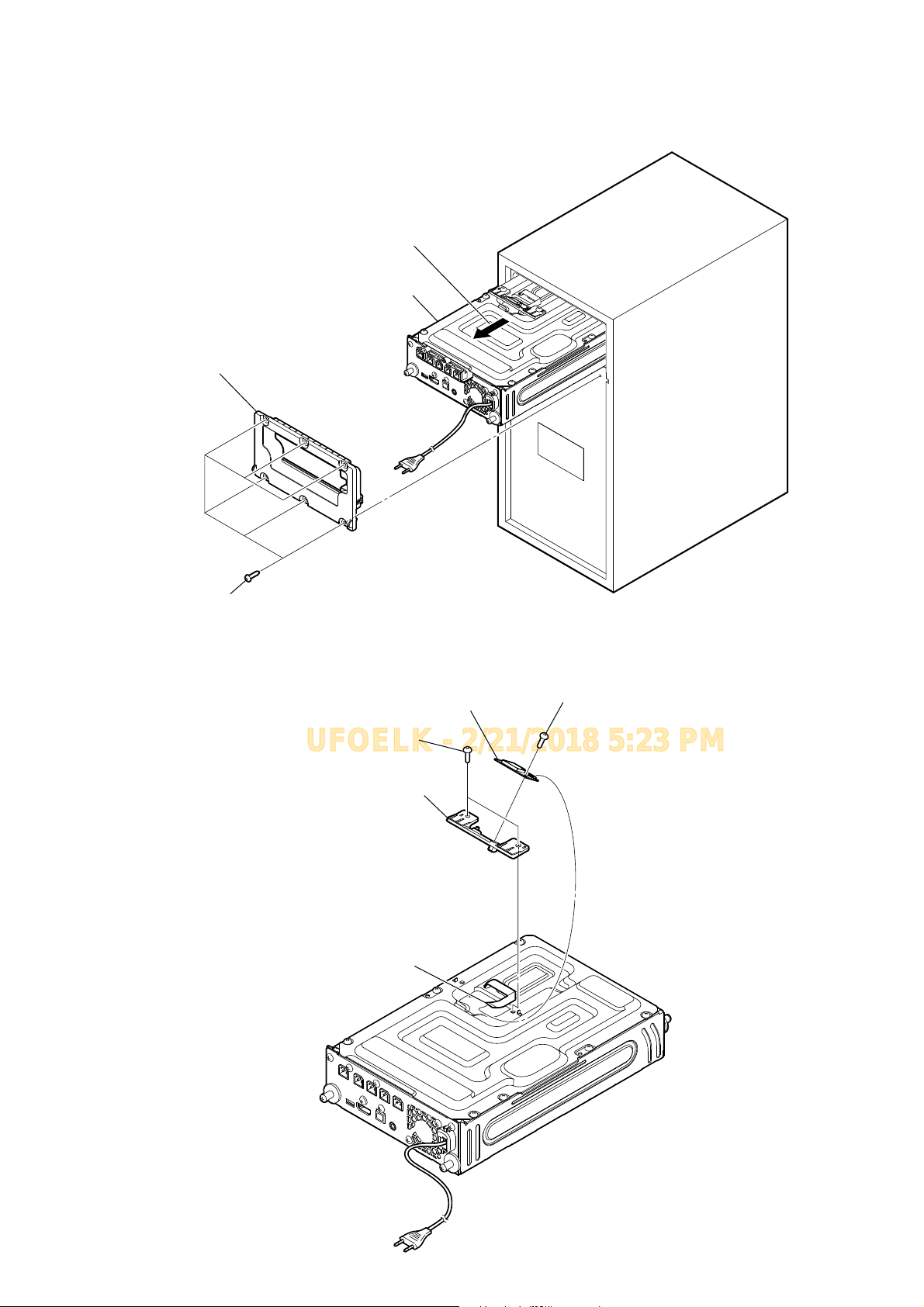
2-4. CHASSIS SECTION
3 Draw out chassis section in
the arrow direction.
2 panel, rear (EL-SW)
HT-RT3
4 chassis section
1 six screws (+BV TAPPING SCREW TYPE-1 3.5)
2-5. BLUETOOTH MODULE
4 two screws (+BVTP 3 x 8)
UFOELK - 2/21/2018 5:23 PM
1 wire (flat type) (18 core)
3 BLUETOOTH module
5 holder, BT
– Rear view –
2 one screw (+BVTP 3 x 8)
– Rear view –
11
Page 12

HT-RT3
2-6. SPEAKER CHUKEI PC BOAR BOARD
1
seven screws (+BVTP 3 x 8)
7
one screw (+BVTP 3 x 8)
8
SPEAKER CHUKEI PC
BOAR board
6
two screws
(+BV3 (3-CR))
4
chassis, top (EL-SW)
2
Remove chassis,
top (EL-SW) in the
direction of arrow.
5
CN1002 (12P)
:LUHVHWWLQJ
3 Draw out wire (flat type) (18 core) from
chassis, top (EL-SW).
rear side
wire (flat type) (18 core)
top side
–5HDUYLHZ–
12
Page 13

2-7. MAIN BOARD, CONNECTOR BOARD, SWITCHING REGULATOR
7 heat sink (EL-SW)
Note: When installing the heat sink (EL-SW), spread the compound referring to
6 four screws
(+BVTP 3 x 8)
8 four screws
(+BVTP 3 x 8)
"NOTE OF REPLACING THE IC1000 AND IC1002 ON THE MAIN BOARD
AND THE COMPLETE MAIN BOARD " on page 5.
0 one screw
(+BV3 (3-CR))
1 wire (flat type) (20 core) (CN2006)
qg REGULATOR, SWITCHING 3L405W-2 (EXCEPT E12) /
REGULATOR, SWITCHING 3L405W-3 (E12)
HT-RT3
Ver. 1.1
9 MAIN board
5 one screw (+B 3 x 5)
3 CN3200 (2P)
4 one screw (+BV3 (3-CR))
qa CONNECTOR
board
2 CN101 (9P)
A
qs CN1 (2P)
qd four screws
(+BVTP 3 x 8)
A
– Rear view –
qf Remove REGULATOR,
SWITCHING 3L405W-2 (EXCEPT E12) /
REGULATOR, SWITCHING 3L405W-3 (E12)
from holder, PC board.
UFOELK - 2/21/2018 5:23 PM
• Abbreviation
E12 : 220-240 V AC area in E model
13
Page 14

HT-RT3
SECTION 3
TEST MODE
COLD RESET
The cold reset clears certain data in this system without initialize
Personal Information and some operation data.
Execute this mode when returning the unit to the customers.
Procedure:
1. Touch the [1] touch key on the main unit to turn the power on.
2. Touch the [VOL -] touch key, [INPUT] touch key and [1]
touch key on the main unit simultaneously for fi ve seconds.
3. The message “RESET” appears on the screen display panel.
PANEL TEST
Procedure:
1. Touch the [1] touch key on the main unit to turn the power on.
2. Press button in order of the [u] → [DIMMER] → [m] → [M]
on the remote commander.
(Make the interval when each button is pressed within two sec-
onds).
3. All segments in screen display panel are lighted up and then is
dimmed after a second.
4. In the state of step 3, touch the [INPUT] touch key on the main
unit and “K 0” is displayed on the screen display panel.
5. In the state of step 4, press the [2+] button on the remote
commander. Each time the [2+] button is pressed, the display
changes from model name → destination → MTK version →
BT version → SW version (not available for HT-RT3 model)
in this order, and returns to the model name display.
6. In the state of step 5, press the [2-] button on the remote commander and all segments in screen display panel are lighted up
and then is dimmed after a second.
Releasing method:
To release from this mode, touch the [1] touch key on the main
unit or press the [1] button on the remote commander.
SOFTWARE VERSION CHECK
The software version is displayed.
Procedure:
1. Touch the [1] touch key on the main unit to turn the power on.
2. Press the [MENU] button on the remote commander and the
message “LVL >” is displayed on the screen display panel.
3. Press the [m] button on the remote commander until the message “SYS >” appears.
4. Press the [ENTER] button on the remote commander and the
message “ASTBY” appears.
5. Press the [m] button on the remote commander and the message “VER” appears.
6. Press the [ENTER] button on the remote commander and the
software version “X.XXX” appears.
AMP TEST
Check the software version before execute this mode.
Procedure:
1. Touch the [1] touch key on the main unit to turn the power on.
2. Press button in order of the [u] → [DIMMER] → [2-] →
[M] on the remote commander.
The messsage “MSURE” is displayed on the screen display
panel.
3. In the state of step 2, press [DIMMER] button on the remote
commander.
The message will appear in order of the “THRU”→ “F2S” →
“F2CW” → “FULL” on the screen display panel.
4. In the state of step 3, press [%] button on the remote commander.
The message will appear in order of the “V.N” → “V .MSM” on
the screen display panel.
5. In the state of step 4, press [CLEARAUDIO+] button on the
remote commander.
The message will appear in order of the “VAON” → “V AOFF”
on the screen display panel.
6. In the state of step 5, press [VOICE] button on the remote commander to adjust the volume gain.
It can be adjusted between -3.0 to +3.0 (increase everytime 0.1
step).
Eg: When gain +1.0 dB by pressing the [VOICE] button, the
message “G +1.0” will appear on the screen display panel.
7. In the state of step 6, press [NIGHT] button on the remote
commander to adjust the volume gain.
It can be adjusted between +3.0 to -3.0 (decrease everytime 0.1
step).
Eg: When gain -1.0 dB by pressing the [NIGHT] button, the
message “G -1.0” will appear on the screen display panel.
Releasing method:
For software version 1.031:
To release from this mode, touch the [
unit or press the [1] button on the remote commander. The message “RESET” appears on the screen display panel.
For software version other than 1.031:
Touch the [1] touch key on the main unit or press the [1] button
on the remote commander to exit this mode. Touch again the [1]
touch key on the main unit or press again the [1] button on the
remote commander and the message “RESET” appears on the
screen display panel.
DEMO MODE
The demo mode can be performed.
(This mode is used by shop front)
Procedure:
1. Touch the [1] touch key on the main unit to turn the power on.
2. Touch the [INPUT] touch key and [VOL−] touch key on the
main unit simultaneously for fi ve seconds.
Or press the button on the remote commander as following
order (each buttons press within 5 seconds).
[BACK] → [ENTER] → [INPUT] → [%] → [INPUT] →
[%]
3. The message “DEMO1” is displayed on the screen display
panel, and enter the demo mode, then changed to the setting of
initial value for demo mode.
Releasing method:
Perform the “COLD RESET”.
Note: The demo mode does not release by unplug the AC cord.
USB UPDATE TEST MODE
To update micontroller software through USB.
Procedure:
1. Plug in USB device in power on condition.
2. Touch the [
main unit simultaneously for fi ve seconds.
3. The message “UPDT” appears and then “UD 0” appears on
the screen display panel.
4. If the updating progress succeeds, the message “UD100” appears and back to normal display.
5. If the updating progress fails, the message “U.ERR” appears.
] touch key and [ ] touch key on the
1
] touch key on the main
1
14
Page 15

SECTION 4
TROUBLESHOOTING
1. “PRTCT” is displayed on OLED display after turning the power on
Note: Please remove USB (removable device) before troubleshooting.
“PRTCT” is displayed on the OLED
display after turning the power ON.
Yes
HT-RT3
"PRTCT" is displayed after
removing Bar speaker (FRONT L,
FRONT R, CENTER speakers)
and Surround speaker (SUR L,
SUR R speakers) and turning the
power ON.
"PRTCT" is displayed after plugging
Bar speaker (FRONT L, FRONT R,
CENTER speakers) and turning the
power ON.
"PRTCT" is displayed after plugging
Surround speaker (SUR L, SUR R
speakers) and turning the power
ON.
Replace MAIN board IC1000 and
IC1002 and check "PRTCT" is
displayed.
UFOELK - 2/21/2018 5:23 PM
Yes
Check and replace the loudspeaker
in subwoofer.
No
Yes
Check and replace the loudspeaker
in Bar speaker.
No
Yes
Check and replace the loudspeaker
in Surround speaker.
No
Yes
Replace complete MAIN board.
2. The video of HDMI is not displayed during USB mode
Check MAIN board IC3200
pin 4 is 5V.
Yes
Replace complete MAIN
board.
Check MAIN board IC3200
pin 1 is 3.3V.
Yes
Check MAIN board IC3200
pin 5 is 7.4V ~ 8V.
Yes
Replace IC3200 on MAIN
board.
NoNo
Refer to "Power is not turned
on" on page 17.
No
Replace MAIN board diode
(D3200).
15
Page 16

HT-RT3
Ver. 1.4
3. The sound is not outputted
Check the Subwoofer, Bar speaker
(FRONT L, FRONT R, CENTER
speakers) and Surround speaker
(SUR L, SUR R speakers) are
functionable.
Yes
Check that the signal is inputted to
MAIN board IC1001:
pin 24 (FRONT L, FRONT R speakers)
pin 25 (SUR L, SUR R speakers)
pin 27 (CENTER speaker, Subwoofer)
Yes
Check that the signal is outputted from
MAIN board IC1001:
pin 38, 39 (CENTER speaker)
pin 41 (FRONT L speaker)
pin 43 (FRONT R speaker)
pin 45 (SUR R speaker)
pin 47 (SUR L speaker)
pin 48, 49 (Subwoofer)
No
Replace the speaker which is not
functionable.
No
Replace complete MAIN board.
No
Replace MAIN board IC1001.
Yes
Check that the signal is outputted from
MAIN board IC1000:
pin 27, 28, 32 (CENTER speaker)
pin 35 (FRONT L speaker)
pin 39, 40 (FRONT R speaker)
Yes
Check that the signal is outputted from
MAIN board IC1002:
pin 27, 28, 32 (Subwoofer)
pin 35 (SUR R speaker)
pin 39, 40 (SUR L speaker)
No
Replace MAIN board IC1000.
No
Replace MAIN board IC1002.
16
Page 17

4. Power is not turned on
Power is not turned on.
Yes
HT-RT3
Ver. 1.4
The voltage of the following is 20V/32V
SWITCHING REGULATOR:
Connector (CN101) pin 2 to 4 and 8.
Yes
Check MAIN board IC3205 pin 1 is 12V.
Yes
Check MAIN board connector (CN2006)
pin 14 is 12V.
Yes
Replace complete MAIN board.
No
Replace the SWITCHING REGULATOR.
No
Replace IC3201 on MAIN board.
No
Replace transistor (Q3208) on MAIN board.
UFOELK - 2/21/2018 5:23 PM
17
Page 18

HT-RT3
Ver. 1.3
5. USB cannot be detected
USB cannot be detected.
Yes
Check IC3000 pin 1 is 5.1V.
Yes
Check coil (L3000) pin 1 and
pin 3 are shorted to ground.
Yes
Replace complete MAIN
board.
No
Replace connector
(CN7000) on USB board.
6. Display panel is not functioned
No Display.
Yes
No
Check that there is no
abnormality on USB board
connector (CN7000).
Check voltage of C5008 on
OLED CHUKEI PC BOAR
board is around 12V.
No
Turn OFF the set and
disconnect the WIRE
(FLAT TYPE) from OLED
CHUKEI PC BOAR board.
Check IC3000 pin 4 is 3.3V.
Check IC3000 pin 5 is 5.1V.
Replace IC3000 on MAIN
board.
Check resistance of C5008
Yes
on OLED CHUKEI PC
BOAR board is > MΩ.
Yes
YesYes
No
No
Refer to "Power is not turned
on" on page 17.
No
Replace complete MAIN
board.
Replace C5008 on OLED
CHUKEI PC BOAR board.
Replace Q3208 and L3207
on MAIN board.
Yes
Turn the power ON and
confirm the Display function.
18
Page 19

5-1. BLOCK DIAGRAM - MAIN CONTROL Section -
1)&02'8/(
5&6::
%/8(7227+02'8/(
8$57B5;
%7B%227
087(
8$57B7;
63',)B287
%7B,17
79,1
237,&$/
$1$/2*,1
237,&$/
5(&(,9(5
/
5
&1
-
237,1
UFOELK - 2/21/2018 5:23 PM
$8',2$'&
,&
9,1/
14
'287
9,15
6&./
/5&.
%&. 8
1)&BL$3B76B6&/
1)&BL$3B6'$
1)&B,54
1)&B5)'(7
%7B5;'
%7B%227
%7B087(
%7B7;'
%7B63',)B,1
18
%7B,17
23763',),1
111
$'&B'2
07.B,6B287B0&.118
07.B,6B287B/5&.
07.B,6287B%&.
'$7$B&B6:
07.B,6B287B&+B6/65
'$7$B/B5
6<67(0352&(6625
,&
;7$/
;7$/
$5&B63',)B,1
6)B'2
6)B',
6)B&.
6)B&6
5'5'
5$5$
%$
%$
5&/.
5:(B
&$6B
5$6B
'40
'40
7;3
7;1
7;3
7;1
7;3
7;1
7;&3
7;&1
+'0,B6&/
+'0,B6'$
+3'
$9''B
&(&
HT-RT3
SECTION 5
DIAGRAMS
4
;
0+]
$5&B63',)
6(5,$/)/$6+
,&
'2
32:(5
6833/<
4
',
5
&/.
&6
1
'4'4
$$
%$
%$
&/.
:(
&$6
18
5$6
15
/'40
8'40
6'5$0
,&
816:9
806:9 9,1 9287
5 4
88
84
$5&%8))(5
,&
1
95(*
,&
&217
1
$<
<
$
&1
$5&
'$7$
'$7$
'$7$
'$7$
'$7$
'$7$
&/2&.
&/2&.
6&/
6'$
+273/8*'(7
932:(5
&(&
14
1
4
+'0,287
15
$5&ź
18
HT-RT3
3&217B0$,1B6<67(0
86%B'3
86%B'0
11
'$7$B/B5
'$7$B6/B65
'$7$B&B6:
07.B,6B287B%&.
07.B,6B287B/5&.
07.B,6B287B0&.
&1
'
'
6LJQDOSDWK
>001B
AUDIO SECTION
(Page 20)
$8',2',*,7$/
$8',2$1$/2*
9,'(2
86%
%/8(7227+
1919
Page 20

HT-RT3
Ver. 1.2
5-2. BLOCK DIAGRAM - AUDIO Section -
>001B
MAIN CONTROL SECTION
(Page 19)
DATA L R
DATA SL SR
DATA C SW
MTK I2S OUT MCK
MTK I2S OUT LRCK
MTK I2S OUT BCK
STREAM PROCESSOR
SDIN1
24
25
SDIN2
SDIN427
MCLK11
LRCK22
SCLK23
IC1001
PWM P 7 47
PWM P 4 45
PWM P 8 49
PWM M 8 48
PWM P 3 43
PWM P 2
PWM M 1 38
PWM P 1 39
DIGITAL POWER AMP
IC1002
INPUT A5
INPUT B OUT B
6
OUT A
OUT A 40
L1001
39
35
SL -
SR +
+
SUR L
–
+
SUR R
ONLY FOR SS-SRT3
SPEAKERS
–
INPUT C14
INPUT D15
DIGITAL POWER AMP
IC1000
INPUT A5
RESET
4
OUT C
OUT D 27
OUT D
OUT A
OUT A
L1002
32
28
L1003
39
40
SW+
SW+
SWSW-
CN1001
3
+
-
4
1
2
LOUDSPEAKER
-
TB6000
FR +
+
FRONT R
–
41
INPUT B OUT B6
INPUT C14
INPUT D15
RESET
4
OUT C
OUT D 27
OUT D
35
L1004
32
28
FL +
CTR +
CTR -
+
FRONT L
–
+
CENTER
TB6001
ONLY FOR SS-RT3
SPEAKERS
–
101
OLED CS
Q2001
37
VALID
BUS BUFFER
IC2007
7
G2
5
A2
40
OLED TAS CLK
Y2 3
SDA20SCL21MUTE19PDN18RESET
16
31
113
104
112
TAS SDA
TAS XPND
TAS XMUTE
TAS XRST
SYSTEM PROCESSOR
IC2003 (MAIN board Suffix-12)
IC2009 (MAIN board Suffix-13)
X2001
27MHz
4
XTAL0
3
XTAL1
6LJQDOSDWK
: AUDIO (DIGITAL)
: AUDIO (ANALOG)
HT-RT3
2020
Page 21

5-3. BLOCK DIAGRAM - POWER SUPPLY Section -
REMOTE CONTROL
RECEIVER
IC5001
2 SIRCSOUT
HT-RT3
Ver. 1.2
SYSTEM PROCESSOR
IC2003 (MAIN board Suffix-12)
IC2009 (MAIN board Suffix-13)
29
MTK RESET
28
RESET
IC2001
4
OUT
VDD
UNSW3.3V
2
SWITCHING
Q2003,Q2004
+ 3.3V
JL4004
VOL+
JL4003
VOL-
JL4002
PAIRING
JL4001
INPUT
JL4005
1
NFC MODULE
(RC-S730 (WW))
CLK
DATA
IRQ
RFDET
MFI
IC2006
SCL 6
SDA
2
VOLTAGE DETECTOR
IC4002
UNSW3.3V
D5000
(BT LED)
UFOELK - 2/21/2018 5:23 PM
OLED
2
VDD
CAP SENSE CONTROLLER
IC4001
CS7/GPO3/SH
11
CS0/PS0
1
CS1/PS1
2
CS4/GPO0
8
CS5/GPO1
9
CS6/GPO2
10
CN5002
4
6
3
5
OLED CLK
2
OUT
4
I2C SDA
6 Y1
15
14
16
BUS BUFFER
IC2007
G1 1
A1 2
NFC IRQ
33
NFC RFDET
38
NFC iAP TS SCLI2C SCL
100
NFC iAP SDA
99
TS INTHI/BUZ
32
OLED DC
83
OLED RESET
98
OLED DOUT
41
OLED CS
101
OLED TAS CLK
40
PCONT BT
AMP PROTECT
FAN CTRL
AC CUT
PCONT MAIN SYSTEM
102
116
115
BT 3.3V
34
D 3.3V
CORE1.2V
VSUS OUT
39
+3.3V REG.
Q3209,Q3210
+3.3V REG.
Q3203,Q3204
+1.2V REG.
IC3204
1 6
1
3
DIGITAL POWER AMP
16
17
DIGITAL POWER AMP
16
17
STREAM PROCESSOR
VO
EN
4
USB VSUS
IC3000
FLT
IC1000
FALUT
OTW
IC1002
FALUT
OTW
IC1001
15
FAN MOTOR
DRIVE
Q3211
VCC
IN
EN/EN
EMO1
+5.1V/ +3.3V REG.
UNSW3.3V
5
4
SW5.1V
GVDD 12V
OLED 12V
A 5V
HDMI 5V
DC FAN
FAN 7V
IC3205
3
SW1
VIN1
SW2
+12V REG.
Q3212,Q3213
+12V REG.
Q3207,Q3208
+5V REG.
IC3207
VOUT
CE
+5V REG.
IC3200
VOUT
CONT
+7V REG.
IC3202
VO
FB
EN
VIN2
EN1
VDD
1
VIN
1
VDD
5
14
12 EN2
3 4
4 5
4
2
1
16
5
4
OUT
DC/DC
CONVERTER
IC3201
AC CUT
IC2008
VDD
2
SUB 32V
PVDD 32V
PCONT MAIN SYSTEM
REGULATOR, SWITCHING
3L405W-2 (EXCEPT E12) /
REGULAR, SWITCHING
3L405W-3 (E12)
(AC IN)
8
UNSW12V
HT-RT3
2121
Page 22

HT-RT3
Ver. 1.1
THIS NOTE IS COMMON FOR PRINTED WIRING BOARDS AND SCHEMATIC DIAGRAMS.
(In addition to this, the necessary note is printed in each block.)
For Printed Wiring Boards.
Note:
• X : Parts extracted from the component side.
• Y : Parts extracted from the conductor side.
• f : Internal component.
• : Pattern from the side which enables seeing.
(The other layers’ patterns are not indicated.)
Caution:
Pattern face side:
(Conductor Side)
Parts face side:
(Component Side)
• MAIN board is multi-layer printed board. However, the
patterns of intermediate layers have not been included in
diagrams.
• Indication of transistor.
C
Q
B
E
• Abbreviation
AR : Argentina model
AUS : Australian model
CND : Canadian model
E12 : 220-240 V AC area in E model
EA : Saudi Arabia model
LA9 : Latin-American model
SP : Singapore model
Note 1: When the complete MAIN board is replaced,
refer to “NOTE OF REPLACING THE IC1000
AND IC1002 ON THE MAIN BOARD AND
THE COMPLETE MAIN BOARD” on page 5.
Parts on the pattern face side seen
from the pattern face are indicated.
Parts on the parts face side seen from
the parts face are indicated.
These are omitted.
For Schematic Diagrams.
Note:
• All capacitors are in μF unless otherwise noted. (p: pF)
50 V or less are not indicated except for electrolytics and
tantalums.
• All resistors are in Ω and 1/4 W or less unless otherwise
specifi ed.
• f : Internal component.
• 2 : Nonfl ammable resistor.
• 5 : Fusible resistor.
• C : Panel designation.
Note: The components identifi ed by mark 0 or
dotted line with mark 0 are critical for safety.
Replace only with part number specifi ed.
Note: Les composants identifi és par une marque
0 sont critiques pour la sécurité.
Ne les remplacer que par une piéce portant
le numéro spécifi é.
• A : B+ Line.
• Voltages and waveforms are dc with respect to ground
under no-signal conditions.
no mark : POWER ON
• Voltages are taken with VOM (Input impedance 10 M).
Voltage variations may be noted due to normal production
tolerances.
• Waveforms are taken with a oscilloscope.
Voltage variations may be noted due to normal production
tolerances.
• Circled numbers refer to waveforms.
• Signal path.
F : AUDIO (DIGITAL)
J : AUDIO (ANALOG)
E : VIDEO
L : USB
a : Bluetooth
• Circuit Boards Location
REGULATOR, SWITCHING 3L405W-2 (Except E12) /
REGULATOR, SWITCHING 3L405W-3 (E12)
OLED CHUKEI PC BOAR board
TOUCH board
USB board
BLUETOOTH module
RC-S730 (WW)
SPEAKER CHUKEI PC BOAR board
MAIN board
CONNE C T O R board
Note 2: When the complete MAIN board is replaced,
spread the bond referring to“BOND FIXATION
OF ELECTRIC PARTS” on page 6.
• Abbreviation
AR : Argentina model
AUS : Australian model
CND : Canadian model
E12 : 220-240 V AC area in E model
EA : Saudi Arabia model
LA9 : Latin-American model
SP : Singapore model
HT-RT3
2222
Page 23

5-4. PRINTED WIRING BOARD - MAIN Board - • See page 22 for Circuit Boards Location. • : Uses unleaded solder.
HT-RT3
Ver. 1.2
1
MAIN BOARD
A
(COMPONENT SIDE)
B
(CHASSIS)
LOUDSPEAKER
C
D
E
F
-
-
+
>001P
USB BOARD
CN7001
(Page 27)
(CHASSIS)
2 3 4 5 6 7 8 9 10 11 12 13 14 15 16
REGULATOR, SWITCHING
3L405W-2 (EXCEPT E12) /
REGULAR, SWITCHING
3L405W-3 (E12)
CN1000
1
JL1000
5
CN1001
6
C1058
C1084
6
1
CN3000
5
7
C3006
JL2154
C1057
C1027
1
C1012
C1085
JL1023
JL1022
C1048
JL2158
C1040
C1063
C1047
C1042
C1043
C1041
C1062
C1067
L3000
C2084
C2086
20
19
C2099
C2088
C2124
CN2006
2
1
20
19
4
JL1020
JL2148
C2083
JL1015
C2101
RB2001
~ AC IN
DC FAN
3
CN3200
R2016
R2208
C2116
R2220
(CHASSIS)
R2153
JL2040
C3272
C3249
C1099
C3248
JL2041
R2211
R2060
R2210
C2029
C2030
JL2042
X2001
R2036
R2058
R2062
JL2039
C3256
C2066
C2065
1
54
1
R1014
R1039
R1013
R1030
IC1001
R1003
R1038
C3271
C3203
R3202
R3207
R3205
1
22
JL1013
JL1010
IC1000
JL1005
C1001
C1050
R1004
JL1009
C1004
C1005
44
JL1008
23
C1002
JL1004
C1003
C1006
C1007
R1005
R1006
R1007
JL1012
JL1006
L1003
JL1007
L1004
C1064
C1065
C1066
JL1025
C1023
C1024
JL1028
C1025
C1026
R1012
JL1003
C1019
C1020
C1018
JC1001
R1002
R1001
JC1002
R1011
1
R1024
C1028
C1049
56
R1000
C1021
C1053
C1013
C1061
C1000
R1025
CL1000
C2091
R1010
R1009
C1017
R1037
R1036
17
18
JL1027
JL1026
C1008
C1009
JL1030
JL1024
R3204
R3203
JL1029
L3200
R3214
1
C3235
C3234
JL1033
CN1002
JL1031
13
JL1032
1
IC3201
8
C3201
C3200
C2023
C3222
45
R3215
9
1
C3220
L3202
JL3200
R3231
R2222
R2161
R2217 R2023
C2105
R3287
C3238
R3233
R2218
1
IC3205
8
R2201
R2219
C3239
C3274
R3229
C3242
C3240
L3204
C3266
16
17
L3205
C3243
JL3201
9
R3244
Q2003
Q2004
C3241
IC2008
C2117
3
2
R2017
C2028
C2027
R2205
1
Q2000
R2022
D2000
R2021
4
C3212
L3203
R3232
C3273
1
2
4
3
IC2001
C2025
R2160
C1044
JL1018
JL1014
IC1002
C1059
C1029
L1000
R1015
R1016
R1033
C1051
C1014
28
R1029
JL1035
R1026
C1036
C1060
C1039
JL1036
C1037
JC1003
JL1034
JC1000
29
R1019
1
CN2002
2
BLUETOOTH MODULE
22
1
R1040
JL1002
10
L1002
JL1016
L1001
R2140
R2141
C2102
R2150
C1055
R1032
JL1019
R1027
JL1011
C1033
R1028
JL2152
R1031
JL1021
C1056
JL1017
C1046
C1045
C1031
R2149
C1030
C1032
JL1001
23
44
2
R2026
4
Q3211
R2073
C2085
R2024
R2146
R2066
RB2002
R3247
R3288
R3286
R3248
R2070
R2061
R2065
R2212
C2075
C2074
128
1
IC2003 (Suffix-12)
IC2009 (Suffix-13)
32
33
(CHASSIS)
C3255
R2072
FB2001
R2074
129
RB2003
IC2005
C3277
R2055
RB2004
R2088
IC3202
R2120
JL2161
JL2160
RB2005
R3284
R2118
1
4
JL2162
21
22
6
SERVICE USE
CN2009
5
ANALOG IN
TV IN
OPTICAL
HDMI OUT
$RC ź
FOR
1-980-405-
12, 13
(12, 13)
Q2005
R2214
R2213
R3022
JL3004
IC2006
J3400
1
R3234
2
CN3400
FB3400
3
C3230
C3400
20
1
L3001
L3002
C3015
R3021
R2114
R3017
4
5
1
4
9
8
5
C2103
R3018
1
8
R2117
C3013
CN3001
19
23
R3023
R3020
4
R3019
C3012
1
R2216
C2104
R2116
R3271
R3413
D3205
C3254
8
9
L3206
Q3204
Q3203
5
R3228
R3277
R3226
R2068
R2071
R2121
R2080
R2069
R2119
R2215
R2067
97
96
R3015
R3016
RB2007
RB2009
65
64
R2145
RB2006
R2148
IC3001
RB2008
28
27
UFOELK - 2/21/2018 5:23 PM
MAIN BOARD
G
(CONDUCTOR SIDE)
H
I
J
K
CL2100
C3010
R3010
R3006
CL2102
CL3401
CL3402
C3009
CL2101
>002P
CONNECTOR BOARD
CN5008
(Page 27)
C3403
R3402
R3404
R3408
C3404
R3405
R3403
C3412
C3415
C3414
C3413
CL3403
R3012
R3013
R3014
R3011
D3200
L2004
R3407
C3405
C3409
C3411
C3268
C3406
C3410
1
IC3401
78
R3406
R2083
IC3200
C3211
C3214
R3296
R2129
C3270
R2128
R3418
31452
FB3201
4
14
C2096
CN2006
2
1
>003P
SPEAKER CHUKEI
PC BOAR BOARD
CN6000
(Page 26)
C3269
3
2
IC3207
1
R3206
D3206
C3210
C2095
R3417
R3254
C3204
C2094
R2082
C3208
R2084
C2093
CL3400
C2067
C2068
C2054
C2053
C2052
C2051
C2048
C2047
C2092
C2041
R2085
C2055
R2079
C2069
R2143
C2072
C2070
D2001
R2193
C2003
R2092
R2081
C2056
C2007
R2157
C2050
R2094
R2142
C2049
R2144
C2073
C2100
C2020
C2062
C2061
C2060
C2059
C2058
C2057
C2046
C2040
C2045
L2001
C2043
C2039
R2063
C2076
C2031
C2077
R2039
C2042
C2005
R2054
C2064
R2040
C2009
R2033
C2121
CL3001
C2063
C2033
C2006
C2004
C2022
C2038
R2127
R2064
C2002
C2037
C2008
C2021
C2019
CL3002
R3295
CL1014
R3257
C3227
L2002
C3228
546
7
L2003
IC3204
231
R2126
R2035
R2028
C2107
C3233
R3235
C3231
R3236
C2098
L2000
R2034
R2041
C2118
R2043
R2042
R2048
R2049
CL2143
R2000
C2010
CL2144
R2002
CL2140
1
IC2000
4
Q3210
C3275
CL2145
R2001
C3276
Q3209
R3280
R2004
8
5
R3278
R3242
C2097
R3279
CL2141
C2024
R2015
CL2142
R3269
CL2128
R2202
R2169
R2167
R2014
CL2127
C2109
R2199
IC2007
CL2146
1
4
CL2125
CL2123
CL2122
R2172
C2108
8
5
CL2126
R2168
CL2124
CL1021
Q2001
R2170
R2171
R2164
R2173
R2194
R2165
CL1022
CL1015
CL1017
CL1016
CL1018
CL1019
CL1037
C1098
CN1002
13
Q3208
Q3213
R3250
R3290
R3289
R3251
Q3212
Q3207
C1097
R1008
C1016
C1015
C1022
C1052
CL1005
C1010 C1011
CL2134
CL2137
CL2139
CL2135
CL2138
R3291
CL1007
CL2133
C3264
CL1008
L3207
R1018
CL2132
C1054
C3278
R1017
R2209
CL2131
CL2129
CL1006
L3208
CL2130
CL2136
R3272
R3252
C1038
CL1001
CL1002
CL1020
C1035
C1034
C3005
IC3000
R3004
C3002
4
CL1004
31
CL1010
CL1011
CL1013
CL2121
2
CL2111
CL2117
CL2118
5
C3000
CL2120
R3001
R2139
CL2115
CL1012
CL2109
R2138
CL2107
CL2103
CL2110
CL2104
R2221
CL1023
CL2105
CL2114
CL1003
CL2106
CL2108
CL2119
CL1009
CL3003
CL3000
1-980-405-
12, 13
(12, 13)
HT-RT3
Note 1: When the complete MAIN board is replaced, refer to “NOTE OF REPLACING THE IC1000
AND IC1002 ON THE MAIN BOARD AND THE COMPLETE MAIN BOARD” on page 5.
2323
Note 2: When the complete MAIN board is replaced, spread the bond referring to“BOND FIXA TION
OF ELECTRIC PARTS” on page 6.
Page 24

HT-RT3
5-5. PRINTED WIRING BOARD - OLED CHUKEI PC BOAR Board -
• See page 22 for Circuit Boards Location. • : Uses unleaded solder.
1
2 3 4 56
OLED CHUKEI PC BOAR BOARD
A
(COMPONENT SIDE)
R5001
C5000
4
7
>004P
CN4001
(Page 25)
8
CN5003
1
6
B
C
TOUCH BOARD
3
R5000
2
1
IC5001
R5007
ELEMENT, ORGANIC
C5008
2
111
12 13
CN5002
EL INDICATOR
C5001
10
C5011 C5007
R5004
C5020
R5009
R5002
R5005
R5003
C5010
C5014
R5008
C5018
D5000
CN5004
1
21
CONNECTOR BOARD
>005P
(Page 27)
1-980-596-
D
OLED CHUKEI PC BOAR BOARD
(CONDUCTOR SIDE)
E
F
CL5025
1-980-596-
CN5009
R5006
20
22
CN5005
6
C5015
1
NFC MODULE
(RC-S730 (WW))
11
(11)
11
(11)
5-6. SCHEMATIC DIAGRAM - OLED CHUKEI PC BOAR Board -
1
A
8
7
B
C
NFC MODULE
(RC-S730 (WW))
D
E
2 3 4 5 6 7 8 910
CL5025
R5008
22
D5000
CL-194S-HB8SP-SD-T
R5000
47
CN5003
6P
CN5004
20P
1
UNSW3.3V
2
TS_CLK
3
TS_INT
4
TS_DATA
5
BT_LED
6
GND
UNSW3.3V
20
19
NFC_CLK
18
GND
NFC_DATA
17
16
NFC_IRQ
NFC_RFDET
15
VCC12V
14
OLED_RST
13
12
OLED_CSB
OLED_DC
11
10
OLED_DOUT
9
UNSW3.3V
8
OLED_CLK
GND
7
TS_INT
6
GND
5
TS_CLK
4
GND
3
TS_DATA
2
SIRCS
1
>001S
TOUCH BOARD
CN4001
(Page 25)
>002S
CONNECTOR
BOARD
CN5009
(Page 27)
NFC_GND
OLED CHUKEI PC BOAR BOARD
CN5005
6P
1UNSW3.3V
2NFC_CLK
3
4NFC_DATA
5NFC_IRQ
6NFC_RFDET
C5020
220P
1KR5009
0
R5005
0
R5004
0
R5003
0R5006
0
R5002
C5015
100P
R5001
47
C5000
C5010
1
C5014
1
C5018
100P
IC5001
RS-470
IC5001
RECEIVER
3
4
VCC
3 GND1
1
GND2 1
OUT 2
3
F
CN5002
11P
11O-LED_GND
VCC12V
10
9
VCC12V
G
ELEMENT,
ORGANIC
EL INDICATOR
O-LED_IREF
O-LED_RESET
O-LED_DOUT
UNSW3.3V
O-LED_CSB
O-LED_DC
O-LED_CLK
8
7
6
5
4
3
2
1O-LED_IXS
R5007
39K
C5007
C5011
0.1
0.1
10C5008 0.1C5001
H
HT-RT3
2424
Page 25

5-7. PRINTED WIRING BOARD - TOUCH Board - • See page 22 for Circuit Boards Location. • : Uses unleaded solder.
HT-RT3
1
2 3 4 5 6 7 8910 11 12 13 14 15 16 17
TOUCH BOARD TOUCH BOARD
A
(COMPONENT SIDE)
R4013
R4014
JL4005
1
JL4001
INPUT
JL4002
PAIRING
JL4003
VOL-
JL4004
VOL+
11
1-980-707-
(11)
R4001
UFOELK - 2/21/2018 5:23 PM
R4003
IC4002
B
>004P
OLED CHUKEI PC
BOAR BOARD
CN5003
(Page 24)
R4002
3
C4005
C4004
4
7
1
CN4001
6
8
IC4001
R4008
R4009
R4010
2
12
9
8
13
1
17
16
C4003
5
C4002
4
1
C4001
C4000
R4005
R4007
R4000
C
D
5-8. SCHEMATIC DIAGRAM - TOUCH Board - • See page 29 for IC Block Diagrams. • See page 29 for IC Pin Function Descriptions.
1
2 3 4 5 6 7 8 9 10 11 12 13
(CONDUCTOR SIDE)
1-980-707-
11
(11)
A
TOUCH BOARD
B
VOLTAGE DETECTOR
1
GND
2
VDD
22
IC4002
PST8429UL
IC4002
R4015
0
OUT
3.1
4
0.3
3
CD
C4004
0.0047
C4005
0.0047
CN4001
6P
22R4000
22R4001
22R4002
0R4003
6 UNSW3.3V
5TS_CLK
4TS_INT
3TS_DATA
2 BT_LED
1GND
>001S
OLED CHUKEI
PC BOAR BOARD
CN5003
(Page 24)
C4000
0.0022
C4001
C
C4002
D
E
C4003
0.1
1
R4010
560
0.1
3.4
5
VDDIO
3.4
6
VDD
7
VSS
CAP SENSE CONTROLLER
0
8
CS4/GPO0
0 0 01.3
R4008
560
R4005
560
1
2
3
4
VCC
CMOD
CS1/PS1
IC4001
CY8CMBR3108
IC4001
CS5/GPO1
CS6/GPO210CS7/GPO3/SH
9
11
12
R4009
560
R4007
560
000.31.9
CS0/PS0
HI/BUZ
I2C_SCL
I2C_SDA
CS2/GUARD
R4011
0
CS3
R4014
5.6K
C4007
10P
3.4
R4013
3.4
16
3.4
15
3.4
14
13
HT-RT3
F
JL4003 JL4002 JL4001JL4004
INPUTPAIRINGVOL-VOL+
JL4005
1
G
2525
Page 26

HT-RT3
5-9. PRINTED WIRING BOARD - SPEAKER CHUKEI PC BOAR Board -
• See page 22 for Circuit Boards Location. • : Uses unleaded solder.
1
2 3 4 56
SPEAKER CHUKEI PC BOAR BOARD
A
(COMPONENT SIDE)
ONLY FOR
SS-SRT3
B
C
D
IN
OUT
C6000
C6003
C6001C6002
C6026 C6027
R6001
IN
OUT
C6015
C6018
C6016C6017
C6028 C6029
R6002
C6014
TB6000
E
SPEAKERS
IN
OUT
C6012
C6030 C6031
C6019
R6003
C6010C6011
C6009
ONLY FOR
SS-RT3
FRONT RFRONT LSUR RSUR L
IN
OUT
C6008
C6032 C6033
C6013
CN6000
R6004
C6006C6007
C6005
C6004
CENTER
IN
OUT
TB6001
C6023
C6020
C6021
C6022
C6024
C6025
JL6000
113
(CHASSIS)
5-10. SCHEMATIC DIAGRAM - SPEAKER CHUKEI PC BOAR Board -
1
2 3 4 5 6 7 8 109
JL6000
A
SPEAKER CHUKEI PC BOAR BOARD
C6023
C6022
0.01
C6002
0.01
C6017
0.01
C6012
0.01
C6024
0.047
C6026
0.047
C6028
0.047
C6030
0.047
B
C
D
MAIN BOARD
CN1002
E
SL +
SR +
SR -
CTR +
CTR +
CTR -
CTR -
SL -
FL+
FR+
FR-
CN6000
13P
13
12
11
10
9
FL-
8
7
6
5
4
3
1
C6014
1000
C6019
1000
C6013
1000
0.001
C6003
0.001
C6018
0.001
C6011
0.001
C6025
0.047
C6027
0.047
C6029
0.047
C6031
0.047
C6020
0.001
C6000
0.001
C6015
0.001
C6010
0.001
C6021
0.01
C6001
0.01
C6016
0.01
C6009
0.01
R6001
100K
R6002
100K
R6003
100K
CL6001
CL6000
TB6001
TB6000
+
-
CENTER
ONLY FOR SS-RT3
SPEAKERS
+
BLU
SUR L
-
+
GRY
SUR R
-
+
WHT
FRONT L
-
+
RED
FRONT R
-
ONLY FOR SS-SRT3
ONLY FOR SS-RT3
F
SPEAKER CHUKEI PC BOAR BOARD
(CONDUCTOR SIDE)
G
H
I
>003P
MAIN BOARD
CN1002
(Page 23)
1-980-597-
1-980-597-
11
(11)
11
(11)
C6004
1000
C6008
0.01
C6032
0.047
C6033
0.047
C6006
0.001
C6005
0.01
R6004
100K
C6007
0.001
F
G
HT-RT3
2626
Page 27

HT-RT3
5-11. PRINTED WIRING BOARD - CONNECTOR Board -
• See page 22 for Circuit Boards Location. • : Uses unleaded solder.
1
23 4
CONNECTOR BOARD
A
(COMPONENT SIDE)
>005P
OLED CHUKEI PC
20
CN5009
B
19
C
D
UFOELK - 2/21/2018 5:23 PM
R5112
1
21
R5111
R5109
CN5008
>002P
MAIN BOARD
CN2006
(Page 23)
R5108
2
1
20
22
BOAR BOARD
CN5004
(Page 24)
1-980-901-
11
(11)
CONNECTOR BOARD
(CONDUCTOR SIDE)
5-13. PRINTED WIRING BOARD - USB Board -
• See page 22 for Circuit Boards Location. • : Uses unleaded solder.
1
2 34
USB BOARD
A
(COMPONENT SIDE)
>001P
MAIN BOARD
CN3000
CN7001
C7001
C7002
1
(Page 23)
B
6
4
1
CN7000
75
6
C7004
C7000
C7003
C
11
1-980-598-
(11)
USB BOARD
D
(CONDUCTOR SIDE)
E
F
(CHASSIS)
1-980-901-
11
(11)
5-12. SCHEMATIC DIAGRAM - CONNECTOR Board -
1
A
B
>002S
OLED CHUKEI
PC BOAR BOARD
CN5004
(Page 24)
C
2 3 45
CONNECTOR BOARD
UNSW3.3V
NFC_CLK
GND
NFC_DATA
NFC_IRQ
NFC_RFDET
VCC12V
OLED_RST
OLED_CSB
OLED_DC
OLED_DOUT
UNSW3.3V
OLED_CLK
GND
TS_INT
GND
TS_CLK
GND
TS_DATA
SIRCS
CN5009
20P
20
19
18
17
16
15
14
13
12
11
10
9
8
7
6
5
4
3
2
1
CN5008
20P
UNSW3.3V
20
19
NFC_CLK
18
GND
NFC_DATA
17
16
NFC_IRQ
NFC_RFDET
15
VCC12V
14
OLED_RST
13
12
OLED_CSB
OLED_DC
0R5108
0R5109
0R5111
0R5112
11
10
OLED_DOUT
9
UNSW3.3V
8
OLED_CLK
GND
7
TS_INT
6
GND
5
TS_CLK
4
GND
3
TS_DATA
2
SIRCS
1
MAIN BOARD
CN2006
E
11
F
1-980-598-
(11)
HT-RT3
D
2727
Page 28

HT-RT3
MEMO
HT-RT3
2828
Page 29

• IC Block Diagrams
IC4002 PST8429UL (TOUCH BOARD)
GND 1
VREF
+
–
OUT4
3
VDD
2
CD
• IC Pin Function Descriptions
TOUCH BOARD IC4001 CY8CMBR3108-LQXIT (TOUCH KEY CONTROLLER)
Pin No. Pin Name I/O Description
1, 2 CS0/PS0, CS1/PS1 - Fixed at “L” in this unit
3 CMOD - External capacitor connection terminal
4 VCC O Internal regulator output terminal
5 VDDIO - Power supply terminal (+3.3V)
6 VDD - Power supply terminal (+3.3V)
7 VSS - Ground terminal
8 CS4/GPO0 I/O Touch key input/output terminal Not used
9 CS5/GPO1 I VOL + touch key input terminal
10 CS6/GPO2 I VOL – touch key input terminal
11 CS7/GPO3/SH I PAIRING touch key input terminal
12 CS2/GUARD I
13 CS3 I Power touch key input terminal
14 I2C_SDA I/O Two-way I2C serial data bus with system controller
15 I2C_SCL I/O Two-way I2C serial data transfer clock signal bus with system controller
16 HI/BUZ O Interrupt signal output to the system controller
INPUT touch key input terminal
HT-RT3
Ver. 1.1
UFOELK - 2/21/2018 5:23 PM
29
Page 30

HT-RT3
Ver. 1.3
Note:
• -XX and -X mean standardized parts, so
they may have some difference from the
original one.
• Items marked “*” are not stocked since
they are seldom required for routine service. Some delay should be anticipated
when ordering these items.
• The mechanical parts with no reference
number in the exploded views are not supplied.
• Color Indication of Appearance Parts Example:
KNOB, BALANCE (WHITE) . . . (RED)
6-1. OVERALL SECTION
Parts Color Cabinet’s Color
8
SECTION 6
EXPLODED VIEWS
• Abbreviation
AR : Argentina model
AUS : Australian model
CND : Canadian model
E12 : 220-240 V AC area in E model
EA : Saudi Arabia model
LA9 : Latin-American model
SP : Singapore model
The components identifi ed by mark 0
or dotted line with mark 0 are critical for
safety.
Replace only with part number specifi ed.
Les composants identifi és par une marque
0 sont critiques pour la sécurité.
Ne les remplacer que par une pièce portant
le numéro spécifi é.
TOUCH board (ns)
The components identifi ed by mark 9 con-
tain confi dential information.
Strictly follow the instructions whenever the
components are repaired and/or replaced.
Les composants identifi és par la marque
9 contiennent des informations confi denti-
elles.
Suivre scrupuleusement les instructions
chaque fois qu’un composant est remplacé
et / ou réparé.
ns
4
#1
chassis section
5
3
ns
OLED CHUKEI PC
BOAR board (ns)
7
4
A
6
#1
ns
A
ns
2
ns
9
1
10
ns
11
ns
Note 2: When the RC-S730 (WW) is replaced, refer
“NOTE OF REPLACING BLUETOOTH MODULE OR RC-S730 (WW)” on page 5.
Ref. No. Part No. Description Remark Ref. No. Part No. Description Remark
1 X-2592-789-1 PANEL, FRONT (EL-SW) ASSY
2 A-2089-365-A USB BOARD, COMPLETE
3 8-989-602-00 RC-S730 (WW)
4 1-828-156-51 WIRE (FLAT TYPE) (6 CORE)
5 4-459-006-01 DOUBLE ADHESIVE TAPE (NFC)
6 1-828-230-51 WIRE (FLAT TYPE) (20 CORE)
7 1-812-049-11 ELEMENT, ORGANIC EL INDICATOR
8 4-586-705-11 DOUBLE ADHESIVE TAPE
9 4-238-407-12 SCREW (1) (4X20), +BV TAPPING
10 1-859-169-21 LOUDSPEAKER 16CM
11 2-682-469-11 FOOT (SW)
#1 7-685-646-71 SCREW +BVTP 3X8 TYPE2 IT-3
ns not supplied
Note 1: If wire (fl at type) is replaced, install it after bend-
ing it in the same form as that before replacement.
30
Page 31

6-2. CHASSIS SECTION
HT-RT3
Ver. 1.3
MAIN board section
#1
ns
#1
ns
55
#1
54
ns
53
ns
#2
52
51
53
UFOELK - 2/21/2018 5:23 PM
ns
#2
Note 1: If wire (fl at type) is replaced, install it after bend-
ing it in the same form as that before replacement.
Note 2: When the BLUETOOTH MODULE is replaced,
refer “NOTE OF REPLACING BLUETOOTH
MODULE OR RC-S730 (WW)” on page 5.
Ref. No. Part No. Description Remark Ref. No. Part No. Description Remark
51 4-874-614-32 +BV TAPPING SCREW TYPE-1 3.5
52 4-582-968-01 PANEL, REAR (EL-SW)
53 4-587-548-01 CATCHER, RUBBER (EL-SW)
54 1-828-218-51 WIRE (FLAT TYPE) (18 CORE)
55 1-493-097-11 BLUETOOTH MODULE
#1 7-685-646-71 SCREW +BVTP 3X8 TYPE2 IT-3
#2 7-685-650-79 SCREW +BVTP 3X16 TYPE2 IT-3
ns not supplied
31
Page 32

HT-RT3
Ver. 1.1
6-3. MAIN BOARD SECTION
#1
#1
A
B
SPEAKER CHUKEI PC
BOAR board (ns)
#1
103
ns
B
E
A
ns
102
C
101
104
CONNECTOR board (ns)
ns
E
D
#1
C
107
D
ns
101
101
Note 4: When the complete MAIN board is replaced,
spread the bond referring to“BOND FIXATION OF
ELECTRIC PARTS” on page 6.
Ref. No. Part No. Description Remark Ref. No. Part No. Description Remark
101 3-077-331-41 +BV3 (3-CR)
0 102 1-855-244-11 DC FAN
9 103 A-2107-088-A MAIN BOARD, COMPLETE (for SERVICE)
9 103 A-2107-150-A MAIN BOARD, COMPLETE (for SERVICE) (AEP)
9 103 A-2107-159-A MAIN BOARD, COMPLETE (for SERVICE) (UK)
9 103 A-2107-210-A MAIN BOARD, COMPLETE (for SERVICE) (E12)
9 103 A-2107-762-A MAIN BOARD, COMPLETE (for SERVICE) (AUS)
9 103 A-2107-776-A MAIN BOARD, COMPLETE (for SERVICE) (SP)
9 103 A-2107-842-A MAIN BOARD, COMPLETE (for SERVICE) (LA9)
9 103 A-2107-983-A MAIN BOARD, COMPLETE (for SERVICE) (AR)
9 103 A-2119-853-A MAIN BOARD, COMPLETE (for SERVICE) (EA)
104 1-828-228-51 WIRE (FLAT TYPE) (20 CORE)
#3
101
101
105
(US, CND)
ns
Note 1: When the complete MAIN board is replaced, re-
106
Note 2: When the REGULATOR, SWITCHING 3L405W
Note 3: If wire (fl at type) is replaced, install it after bending
0 105 4-966-267-12 BUSHING (FBS001), CORD
0 106 1-834-966-42 POWER-SUPPLY CORD (AEP, SP, LA9)
0 106 1-835-068-21 CORD, POWER (AUS)
0 106 1-837-308-12 CORD, POWER-SUPPLY (US, CND)
0 106 1-837-312-11 CORD, POWER-SUPPLY (AR)
0 106 1-839-999-22 POWER-SUPPLY CORD (UK, EA)
0 106 1-848-053-12 POWER-SUPPLY CORD (E12)
0 107 1-474-638-11 REGULATOR, SWITCHING 3L405W-2
0 107 1-474-638-21 REGULATOR, SWITCHING 3L405W-3 (E12)
#1 7-685-646-71 SCREW +BVTP 3X8 TYPE2 IT-3
#3 7-682-546-09 SCREW +B 3X5
ns not supplied
fer to “NOTE OF REPLACING THE IC1000 AND
IC1002 ON THE MAIN BOARD AND THE COMPLETE MAIN BOARD” on page 5.
board is replaced, spread the bond referring to
“BOND FIXATION OF ELECTRIC PARTS” on
page 6.
it in the same form as that before replacement.
(EXCEPT E12)
32
Page 33

Note:
• Due to standardization, replacements in
the parts list may be different from the
parts specifi ed in the diagrams or the com-
ponents used on the set.
• -XX and -X mean standardized parts, so
they may have some difference from the
original one.
• Items marked “*” are not stocked since
they are seldom required for routine service. Some delay should be anticipated
when ordering these items.
• RESISTORS
All resistors are in ohms.
METAL: Metal-fi lm resistor.
METAL OXIDE: Metal oxide-fi lm resistor .
F: nonfl ammable
SECTION 7
ELECTRICAL PARTS LIST
• CAPACITORS
uF: μF
• COILS
uH: μH
• SEMICONDUCTORS
In each case, u: μ, for example:
uA. . : μA. . , uPA. . , μPA. . ,
uPB. . : μPB. . , uPC. . , μPC. . ,
uPD. . : μPD. .
• Abbreviation
AR : Argentina model
AUS : Australian model
CND : Canadian model
E12 : 220-240 V AC area in E model
EA : Saudi Arabia model
LA9 : Latin-American model
SP : Singapore model
HT-RT3
Ver. 1.5
MAINCONNECTOR
SPEAKER CHUKEI PC BOAROLED CHUKEI PC BOAR
When indicating parts by reference number, please include the board name.
The components identifi ed by mark 0
or dotted line with mark 0 are critical for
safety.
Replace only with part number specifi ed.
Les composants identifi és par une marque
0 sont critiques pour la sécurité.
Ne les remplacer que par une pièce portant
le numéro spécifi é.
The components identifi ed by mark 9 con-
tain confi dential information.
Strictly follow the instructions whenever the
components are repaired and/or replaced.
Les composants identifi és par la marque
9 contiennent des informations confi denti-
elles.
Suivre scrupuleusement les instructions
chaque fois qu’un composant est remplacé
et / ou réparé.
Ref. No. Part No. Description Remark Ref. No. Part No. Description Remark
CONNECTOR BOARD
*****************
< CONNECTOR >
UFOELK - 2/21/2018 5:23 PM
CN5008 1-842-052-21 CONNECTOR, FFC/FPC (LIF) 20P
CN5009 1-793-331-31 CONNECTOR, FFC/FPC (LIF) 20P
*************************************************************
9 A-2107-088-A MAIN BOARD, COMPLETE (for SERVICE)
9 A-2107-150-A MAIN BOARD, COMPLETE (for SERVICE) (AEP)
9 A-2107-159-A MAIN BOARD, COMPLETE (for SERVICE) (UK)
9 A-2107-210-A MAIN BOARD, COMPLETE (for SERVICE) (E12)
9 A-2107-762-A MAIN BOARD, COMPLETE (for SERVICE) (AUS)
9 A-2107-776-A MAIN BOARD, COMPLETE (for SERVICE) (SP)
9 A-2107-842-A MAIN BOARD, COMPLETE (for SERVICE) (LA9)
9 A-2107-983-A MAIN BOARD, COMPLETE (for SERVICE) (AR)
9 A-2119-853-A MAIN BOARD, COMPLETE (for SERVICE) (EA)
*********************
< DIODE >
D3200 6-503-735-01 DI BZT52H-C4V3
< IC >
IC1000 6-721-742-01 IC TAS5614LA
IC1001 6-718-103-01 IC TAS5538DGGR
IC1002 6-721-742-01 IC TAS5614LA
IC2003 6-722-554-01 IC CXD90040R-B (MAIN board Suffi x-12)
IC2005 6-720-801-01 IC EM638165TSD-6G
(US, CND)
IC3204 6-720-509-01 IC BD00IC0WHFV-GTR
< COIL >
L3207 1-246-226-11 METAL CHIP 15 0.5% 1/8W
< TRANSISTOR >
Q3208 6-553-482-01 TR SSM3J56MFV
*************************************************************
OLED CHUKEI PC BOAR BOARD
**************************
< CAPACITOR >
C5008 1-118-047-11 CERAMIC CHIP 10uF 10% 16V
< CONNECTOR >
CN5002 1-843-407-31 FPC CONNECTOR (ZIF) (11PIN)
CN5003 1-816-654-61 FFC/CONNECTOR, FPC (LIF) 6P
CN5004 1-842-052-21 CONNECTOR, FFC/FPC (LIF) 20P
CN5005 1-816-654-61 FFC/CONNECTOR, FPC (LIF) 6P
< DIODE >
D5000 6-503-196-01 DI CL-194S-HB8SP-SD-T
< IC >
IC5001 6-600-629-01 IC RS-470
*************************************************************
IC2009 6-722-554-01 IC CXD90040R-B (MAIN board Suffi x-13)
IC3000 6-720-030-01 IC TPS2065CDBVR
IC3001 6-722-615-01 IC TC7WHU04FK,RSNJ (CT
IC3200 6-718-999-01 IC MM1839A50NRE
IC3201 6-721-694-01 IC RT7272BGSP
Note 1: When the complete MAIN board is replaced, re-
fer to “NOTE OF REPLACING THE IC1000 AND
IC1002 ON THE MAIN BOARD AND THE COMPLETE MAIN BOARD” on page 5.
Note 2: When the complete MAIN board is replaced,
spread the bond referring to“BOND FIXATION OF
ELECTRIC PARTS” on page 6.
SPEAKER CHUKEI PC BOAR BOARD
*****************************
< TRANSFORMER >
TB6000 1-780-454-11 TERMINAL BOARD (SPEAKER) 4P
TB6001 1-780-815-11 TERMINAL BOARD (SPEAKER)
*************************************************************
33
Page 34

HT-RT3
Ver. 1.3
TOUCH
Ref. No. Part No. Description Remark Ref. No. Part No. Description Remark
TOUCH BOARD
************
USB
ACCESSORIES
************
< CONNECTOR >
CN4001 1-816-654-61 FFC/CONNECTOR, FPC (LIF) 6P
< IC >
IC4001 6-722-496-01 IC CY8CMBR3108-LQXIT
IC4002 6-713-333-01 IC PST8429UL
*************************************************************
A-2089-365-A USB BOARD, COMPLETE
********************
< CONNECTOR >
CN7000 1-843-975-11 USB CONNECTOR (A)
*************************************************************
MISCELLANEOUS
**************
3 8-989-602-00 RC-S730 (WW)
4 1-828-156-51 WIRE (FLAT TYPE) (6 CORE)
6 1-828-230-51 WIRE (FLAT TYPE) (20 CORE)
10 1-859-169-21 LOUDSPEAKER 16CM
54 1-828-218-51 WIRE (FLAT TYPE) (18 CORE)
55 1-493-097-11 BLUETOOTH MODULE
0 102 1-855-244-11 DC FAN
104 1-828-228-51 WIRE (FLAT TYPE) (20 CORE)
0 105 4-966-267-12 BUSHING (FBS001), CORD
0 106 1-834-966-42 POWER-SUPPLY CORD (AEP, SP, LA9)
4-587-771-13 MANUAL, INSTRUCTION
(ENGLISH (US), LATIN SPANISH, CANADIAN
4-587-771-21 MANUAL, INSTRUCTION
4-587-771-31 MANUAL, INSTRUCTION
4-587-771-41 MANUAL, INSTRUCTION
4-587-771-51 MANUAL, INSTRUCTION
(TRADITIONAL CHINESE, FRENCH, ARABIC,
4-587-771-61 MANUAL, INSTRUCTION
4-587-771-71 MANUAL, INSTRUCTION (LATIN SPANISH) (LA9)
4-587-771-81 MANUAL, INSTRUCTION (LATIN SPANISH) (AR)
501 1-493-155-11 REMOTE COMMANDER RMT-AH200U
502 1-848-225-21 CABLE, LIGHT PLUG (Optical digital cable)
503 1-849-353-11 HDMI CABLE (High Speed HDMI cable)
0 504 1-785-504-21 ADAPTOR, CONVERSION (AC plug adaptor) (LA9)
501 Remote control (1) 502 Optical digital cable (1)
(ENGLISH) (UK, SP, AUS, E12)
(FRENCH, SPANISH, GERMAN) (AEP)
(DUTCH, ITALIAN, POLISH) (AEP)
(US, CND, AEP, UK)
FRENCH) (US, CND)
PERSIAN) (SP)
(ENGLISH, ARABIC) (EA)
(Remote control)
(US, CND, AEP, UK)
(EA, SP, AR, AUS, E12, LA9)
0 106 1-835-068-21 CORD, POWER (AUS)
0 106 1-837-308-12 CORD, POWER-SUPPLY (US, CND)
0 106 1-837-312-11 CORD, POWER-SUPPLY (AR)
0 106 1-839-999-22 POWER-SUPPLY CORD (UK, EA)
0 106 1-848-053-12 POWER-SUPPLY CORD (E12)
0 107 1-474-638-11 REGULATOR, SWITCHING 3L405W-2
(EXCEPT E12)
0 107 1-474-638-21 REGULATOR, SWITCHING 3L405W-3 (E12)
*************************************************************
Note 1: If wire (fl at type) is replaced, install it after bending it
in the same form as that before replacement.
Note 2: When the REGULATOR, SWITCHING 3L405W
board is replaced, spread the bond referring to
“BOND FIXATION OF ELECTRIC PARTS” on page
6.
503 High Speed HDMI cable (1)
(EA, SP, AR, AUS, E12, LA9)
504 AC plug adaptor* (1) (LA9)
* The adaptor is not use in Chile,
Uruguay and Paraguay. Use the adaptor
in the countries where it is neccessary.
Note 3: When the BLUETOOTH MODULE or RC-S730
(WW) is replaced, refer “NOTE OF REPLACING
BLUETOOTH MODULE OR RC-S730 (WW)” on
page 5.
34
Page 35

MEMO
HT-RT3
UFOELK - 2/21/2018 5:23 PM
35
Page 36

HT-RT3
REVISION HISTORY
Ver. Date Description of Revision
1.0 2016.03 New
1.1 2016.06 Addition of Argentina, Latin-American and Singapore models.
Add Abbreviation for E12 in page 13.
Add IC Pin Function Description of IC4001 in page 29.
Change description of MANUAL, INSTRUCTION for US and Canadian models in ACCESSORIES
section.
Change P/N of POWER-SUPPLY CORD for AEP
Change P/N of Ref. No. 10 in page 34.
Change P/N and description of Ref. No. for TB6001 in SPEAKER CHUKEI PC BOAR board.
Delete of CN2008 and S2000 in MAIN board.
Delete of duplicate WIRE (FLAT TYPE) (6 CORE) in page 30 and 34.
1.2 2016.08 Add “
Change of MAIN board (Suffi x 12,13).
Change of IC2009 and IC3205 to complete MAIN board in page 18.
Change of IC2009 in MAIN board to IC2003 (MAIN board Suffi x-12) and IC2009 (MAIN
board Suffi x-13) in page 20 and 21.
Change of Ref. No. IC1000 to IC1002 in page 20.
Change of Ref. No. IC1002 to IC1000 in page 20.
Change quantity of AC plug adaptor (LA9) in SPECIFICATIONS and ACCESSORIES sections.
0” mark for Ref. No. 504 in ACCESSORIES section.
model in page 32 and page 34.
1.3 2017.02 Add note of “NOTE OF REPLACING BLUETOOTH MODULE OR RC-S730 (WW)” in page 5, 30, 31
and 34.
Add P/N and description of L3207 on MAIN board in page 33.
Add P/N and description of C5008 on OLED CHUKEI PC BOAR board in page 33.
Add troubleshooting fl ow (6. Display panel is not functioned) in page 18.
Change P/N of Ref. No. 10 in page 30 and 34.
1.4 2017.07 Correction of TROUBLESHOOTING
1.5 2017.09 Addition of Part No. for Ref. No. IC2003, IC2005, IC2009, IC3001 and IC3204 on MAIN board (SMR-17027)
(SMR-17020)
How to search for a contact point of signal lines or the like in DIAGRAMS SECTION
If a contact point of a BLOCK DIAGRAM, PRINTED WIRING BOARD or SCHEMATIC DIAGRAM is shown in a different page, use
the PDF fi le search function to fi nd one.
e.g.) If a contact point is shown as , follow the procedure below.
Procedure:
1. Press the [F] key while pressing the [Ctrl] key.
2. Input “>001Z” in the search box and press the [Enter] key.
3. The relevant part (page), where the contact point is shown, appears.
Note: If you still see the original page, press the [Enter] key again.
 Loading...