

Sony HCD-RG190, HCD-RG290 User Manual

HCD-RG190/RG290
SERVICE MANUAL
Ver. 1.2 2006.06
• HCD-RG190 is the amplifier, CD player, tape
deck and tuner section in MHC-RG190.
• HCD-RG290 is the amplifier, CD player, tape
deck and tuner section in MHC-RG290.
Model Name Using Similar Mechanism HCD-RG490/RG590
CD Mechanism Type
CD
Section Base Unit Name
Optical Pick-up Block Name
TAPE Model Name Using Similar Mechanism HCD-RG490/RG590
Section Tape Transport Mechanism Type CWN42FF609
Photo: HCD-RG290
AEP Model
E Model
Australian Model
HCD-RG190/RG290
UK Model
Mexican Model
HCD-RG290
CDM74KF-K6BD83S (Except Mexican model)/
CDM74KF-F1BD84 (Mexican model)
BU-K6BD83S-WOD (Except Mexican model)/
BU-F1BD84 (Mexican model)
KSM-213DHAP (Except Mexican model)/
KSM-215DCP (Mexican model)
Amplifier Section
HCD-RG290
The following are measured at AC 120, 127,
220, 240 V 50/60 Hz
DIN power output (rated): 95 + 95 watts
(6 ohms at 1 kHz, DIN)
Continuous RMS power output
(reference): 125 + 125 watts (6 ohms at 1
kHz, 10% THD)
HCD-RG190
The following are measured at AC 120, 127,
220, 240 V 50/60 Hz
DIN power output (rated): 50 + 50 watts
(6 ohms at 1 kHz, DIN)
Continuous RMS power output
(reference): 65 + 65 watts (6 ohms at 1
kHz, 10% THD)
Inputs:
AUDIO IN (stereo mini jack): voltage 250
mV, impedance 47 kilohms
MIC (phone jack) (Latin American model
only): sensitivity 1 mV, impedance 10
kilohms
SPECIFICATIONS
Outputs:
PHONES (stereo mini jack): accepts
headphones of 8 ohms or more
VIDEO OUT (phono jack) (Mexican
model only): max. output level 1Vpp,
unbalanced, Sync negative, load
impedance 75 ohms
SPEAKER: accepts impedance of 6 to 16
ohms
CD player section
System: Compact disc and digital audio system
Laser Diode Properties
Emission duration: continuous Laser
Output*: Less than 44.6µW
*This output is the value measurement at a
distance of 200mm from the objective lens
surface on the Optical Pick-up Block with
7mm aperture.
Frequency response: 20 Hz – 20 kHz
Signal-to-noise ratio: More than 90 dB
Dynamic range: More than 90 dB
COMPACT DISC DECK RECEIVER
Tape deck section
Recording system: 4-track 2-channel, stereo
Frequency response: 50 – 13,000 Hz (±3 dB),
using Sony TYPE I cassettes
Tuner section
FM stereo, FM/AM superheterodyne tuner
FM tuner section:
Tuning range
87.5 – 108.0 MHz (50 kHz step)
Antenna: FM lead antenna
Antenna terminals: 75 ohms unbalanced
Intermediate frequency: 10.7 MHz
AM tuner section:
Tuning range
Pan-American model:
530 – 1,710 kHz (with 10 kHz tuning interval)
531 – 1,710 kHz (with 9 kHz tuning interval)
– Continued on next page –
9-887-145-03
2006F05-1
© 2006.06
Sony Corporation
Home Audio Division
Published by Sony Techno Create Corporation

HCD-RG190/RG290
Ver. 1.1
European, Russian and Saudi Arabian models:
531 – 1,602 kHz (with 9 kHz tuning interval)
Other models:
530 – 1,710 kHz (with 10 kHz tuning interval)
531 – 1,602 kHz (with 9 kHz tuning interval)
Antenna: AM loop antenna, external antenna
terminal
Intermediate frequency: 450 kHz
General
Power requirements
European and Russian models: AC 230 V,
50/60 Hz
Australian model: AC 230 – 240V,
50/60 Hz
Mexican model: AC 127V, 60 Hz
Argentine model: AC 220V, 50/60 Hz
Saudi Arabian model: AC 120 – 127, 220
or 230 – 240 V, 50/60 Hz, Adjustable with
voltage selector
Other models: AC 120, 220 or 230 – 240 V,
50/60 Hz, Adjustable with voltage selector
Power consumption
European and Russian models:
HCD-RG290: 185 watts
HCD-RG190: 100 watts
Other models:
HCD-RG290: 200 watts
HCD-RG190: 110 watts
Notes on chip component replacement
• Never reuse a disconnected chip component.
• Notice that the minus side of a tantalum capacitor may be
damaged by heat.
Flexible Circuit Board Repairing
• Keep the temperature of the soldering iron around 270 ˚C
during repairing.
• Do not touch the soldering iron on the same conductor of the
circuit board (within 3 times).
• Be careful not to apply force on the conductor when soldering
or unsoldering.
CAUTION
Use of controls or adjustments or performance of procedures
other than those specified herein may result in hazardous radiation
exposure.
This appliance
is classified
as a CLASS 1
LASER product.
This marking is
located on the rear
exterior.
Dimensions (w/h/d) (excl. speakers): Approx.
280 × 328 × 412.3 mm
Mass (excl. speakers)
HCD-RG290: Approx. 9.3 kg
HCD-RG190: Approx. 7.5 kg
Design and specifications are subject to change
without notice.
SAFETY-RELATED COMPONENT WARNING!!
COMPONENTS IDENTIFIED BY MARK 0 OR DOTTED LINE
WITH MARK 0 ON THE SCHEMATIC DIAGRAMS AND IN
THE PARTS LIST ARE CRITICAL TO SAFE OPERATION.
REPLACE THESE COMPONENTS WITH SONY P ARTS WHOSE
PART NUMBERS APPEAR AS SHOWN IN THIS MANUAL OR
IN SUPPLEMENTS PUBLISHED BY SONY.
2

TABLE OF CONTENTS
HCD-RG190/RG290
1. SERVICING NOTES ............................................... 4
2. GENERAL ................................................................... 5
3. DISASSEMBLY
3-1. Disassembly Flow ........................................................... 6
3-2. Case (Side-L), Case (Side-R) .......................................... 7
3-3. Case (Top) ....................................................................... 7
3-4. LID (CD) ......................................................................... 8
3-5 CD Mechanism Deck
(CDM74KF-K6BD83S: Except Mexican model)
(CDM74KF-F1BD84: Mexican model) .......................... 8
3-6. Front Panel Block............................................................ 9
3-7. Mecha Deck (CWN42FF609) ......................................... 9
3-8. Back Panel Section .......................................................... 10
3-9. MAIN Board.................................................................... 10
3-10. BD Board (Mexican model),
CD Board (Except Mexican model) ................................ 11
3-11. DRIVE Board, SW Board ............................................... 11
3-12. Optical Pick-up Block ..................................................... 12
3-13. SENSOR Board ............................................................... 12
3-14. MOTOR (TB) Board ....................................................... 13
3-15. MOTOR (LD) Board ....................................................... 13
4. TEST MODE.............................................................. 14
5. MECHANICAL ADJUSTMENTS ....................... 17
6. ELECTRICAL ADJUSTMENTS ......................... 18
7. DIAGRAMS
7-1. Block Diagram – CD SERVO Section – ......................... 21
7-2. Block Diagram – MAIN Section –.................................. 22
7-3. Block Diagram – AMP/VIDEO Section – ...................... 23
7-4. Block Diagram
– PANEL/POWER SUPPLY Section – ........................... 24
7-5. Printed Wiring Board – CD Board
(Except RG290: MX model) – ........................................ 26
7-6. Schematic Diagram – CD Board
(Except RG290: MX model) – ........................................ 27
7-7. Printed Wiring Board – BD Board
(RG290: MX model) – .................................................... 28
7-8. Schematic Diagram – BD Board
(RG290: MX model) – .................................................... 29
7-9. Printed Wiring Boards – CHANGER Section – .............. 30
7-10. Schematic Diagram – CHANGER Section – .................. 31
7-11. Printed Wiring Board – DECK Board –.......................... 32
7-12. Schematic Diagram – DECK Board –............................. 33
7-13. Printed Wiring Board – MAIN Board
(Except RG290: MX model) – ........................................ 34
7-14. Schematic Diagram – MAIN Board (1/3)
(Except RG290: MX model) – ........................................ 35
7-15. Schematic Diagram – MAIN Board (2/3)
(Except RG290: MX model) – ........................................ 36
7-16. Schematic Diagram – MAIN Board (3/3)
(Except RG290: MX model) – ........................................ 37
7-17. Printed Wiring Board – MAIN Board
(RG290: MX model) – .................................................... 38
7-18. Schematic Diagram – MAIN Board (1/3)
(RG290: MX model) – .................................................... 39
7-19. Schematic Diagram – MAIN Board (2/3)
(RG290: MX model) – .................................................... 40
7-20. Schematic Diagram – MAIN Board (3/3)
(RG290: MX model) – .................................................... 41
7-21. Printed Wiring Board – MIC. AUX. HP Board –............ 42
7-22. Schematic Diagram – MIC. AUX. HP Board –............... 43
7-23. Printed Wiring Board – POWER Board (RG190) – ........ 44
7-24. Schematic Diagram – POWER Board (RG190) – .......... 45
7-25. Printed Wiring Board – POWER Board (RG290) – ........ 46
7-26. Schematic Diagram – POWER Board (RG290) – .......... 47
7-27. Printed Wiring Boards – CD-G Section
(RG290: MX model) – .................................................... 48
7-28. Schematic Diagram – CD-G Section
(RG290: MX model) – .................................................... 49
7-29. Printed Wiring Board – PANEL Board – ........................ 50
7-30. Printed Wiring Boards – KEY Section –......................... 51
7-31. Schematic Diagram – PANEL/KEY Section – ............... 52
7-32. Printed Wiring Board
– TRANSFORMER Board (RG190) – ........................... 54
7-33. Schematic Diagram
– TRANSFORMER Board (RG190) – ........................... 55
7-34. Printed Wiring Board
– TRANSFORMER Board (RG290) – ........................... 56
7-35. Schematic Diagram
– TRANSFORMER Board (RG290) – ........................... 57
8. EXPLODED VIEWS
8-1. Case Section .................................................................... 74
8-2. PANEL Board Section..................................................... 75
8-3. Lid (Top) Section............................................................. 76
8-4. Front Panel Section ......................................................... 77
8-5. MAIN Board Section....................................................... 78
8-6. POWER Board, SUB WOOFER Board Section ............. 79
8-7. Chassis Section................................................................ 80
8-8. CD Mechanism Deck Section-1
(CDM74KF-K6BD83S) (Except Mexican model)/
(CDM74KF-F1BD84) (Mexican model) ........................ 81
8-9. CD Mechanism Deck Section-2
(CDM74KF-K6BD83S) (Except Mexican model)/
(CDM74KF-F1BD84) (Mexican model) ........................ 82
9. ELECTRICAL PARTS LIST................................ 83
• Abbreviation
MX: Mexican model
3
HCD-RG190/RG290
Ver. 1.1
SECTION 1
SERVICING NOTES
NOTES ON HANDLING THE OPTICAL PICK-UP
BLOCK OR BASE UNIT
The laser diode in the optical pick-up block may suffer electrostatic
break-down because of the potential difference generated by the
charged electrostatic load, etc. on clothing and the human body.
During repair, pay attention to electrostatic break-down and also
use the procedure in the printed matter which is included in the
repair parts.
The flexible board is easily damaged and should be handled with
care.
NOTES ON LASER DIODE EMISSION CHECK
The laser beam on this model is concentrated so as to be focused on
the disc reflective surface by the objective lens in the optical pickup block. Therefore, when checking the laser diode emission,
observe from more than 30 cm away from the objective lens.
UNLEADED SOLDER
Boards requiring use of unleaded solder are printed with the leadfree mark (LF) indicating the solder contains no lead.
(Caution: Some printed circuit boards may not come printed with
the lead free mark due to their particular size)
: LEAD FREE MARK
Unleaded solder has the following characteristics.
• Unleaded solder melts at a temperature about 40 °C higher
than ordinary solder.
Ordinary soldering irons can be used but the iron tip has to be
applied to the solder joint for a slightly longer time.
Soldering irons using a temperature regulator should be set to
about 350 °C.
Caution: The printed pattern (copper foil) may peel away if
the heated tip is applied for too long, so be careful!
• Strong viscosity
Unleaded solder is more viscou-s (sticky, less prone to flow)
than ordinary solder so use caution not to let solder bridges
occur such as on IC pins, etc.
• Usable with ordinary solder
It is best to use only unleaded solder but unleaded solder may
also be added to ordinary solder.
RELEASING THE ANTITHEFT LOCK
The disc table lock function for the antitheft of an demonstration
disc in the store is equipped.
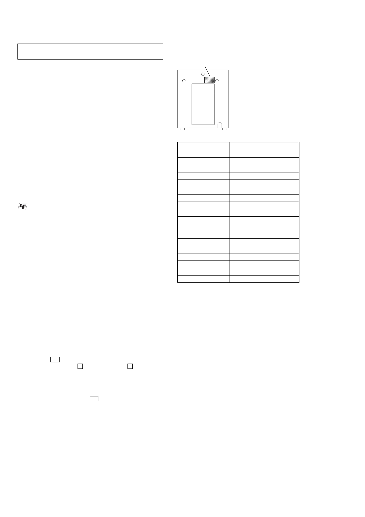
MODEL IDENTIFICATION
– Back Panel –
Model number label
Label indication Model
2-664-545-0[] CED RG290: AEP, UK
2-664-546-0[] E3 RG290: E3
2-664-547-0[] SP2 RG290: SP
2-664-548-0[] AU RG290: AUS
2-664-550-0[] E51 RG290: E51
2-664-551-0[] AR RG290: AR
2-664-552-0[] MX4 RG290: MX
2-664-553-0[] CED RG190: AEP
2-664-554-0[] E3 RG190: E3
2-664-555-0[] SP2 RG190: SP
2-664-556-0[] AU RG190: AUS
2-664-557-0[] EA3 RG190: EA
2-664-558-0[] E51 RG190: E51
2-664-559-0[] AR RG190: AR
2-665-213-0[] E2 RG190: E2
2-666-351-0[] E2 RG290: E2
2-674-578-0[] RU RG290: RU
2-674-579-0[] RU RG190: RU
• Abbreviation
AR : Argentina model
AUS: Australian model
E2 : 120V AC area in E model
E3 : 240V AC area in E model
E51 : Chilean and Peruvian models
EA : Saudi Arabia model
MX : Mexican model
Releasing Procedure :
1. Press the
I/1 button to turn the power on.
2. While pressing the s button, press the A button until
“UNLOCKED” displayed on the fluorescent indicator tube
(around 5 seconds).
Note: When “LOCKED” is displayed, the antitheft lock is not released by
turning power on/off with the I/1 button.
NOTES ON REPLACEMENT OF IC901 ON THE MAIN
BOARD
IC901 on the MAIN board cannot exchange with single. When IC901
is damaged, exchange the entire mounted board.
4
SECTION 2
GENERAL
HCD-RG190/RG290
This section is extracted from
instruction manual.
Guide to parts and
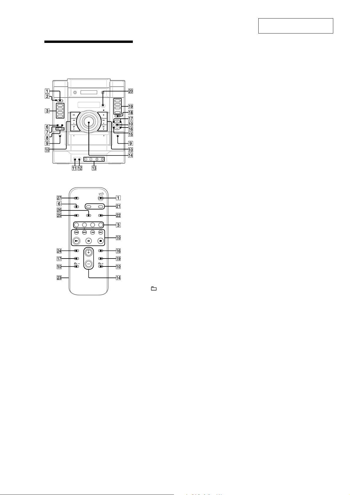
controls
Unit
Remote
6
Mexican model:
Unit: KARAOKE button
Press to activate the karaoke mode.
Remote: DISPLAY button
Press to change the information on the
display.
Other models:
DISPLAY button
Press to change the information on the
display.
7
ILLUMINATION button
Press to change the illumination pattern
around the VOLUME control
8
Buttons for synchro recording or
qf
manual recording
REC PAUSE/START button,
CD SYNC button
Press to record on a tape.
9
PUSH Z
Press to insert or eject a tape.
q;
Playback buttons
Unit: NX (play/pause) button
Remote: N (play) button,
X (pause) button
Press to start or pause playback.
x (stop) button
Press to stop playback.
./> (go back/go forward)
Press to select a track or file.
Unit: TUNING +/– button
Remote: +/– (tuning) button
Press to tune in the desired station.
+/– (select folder) button
Press to select a folder on an MP3 disc.
qf
Unit: V OLUME control
Turn to adjust the volume.
Remote: VOLUME +/– button
Press to adjust the volume.
qg
EQ BAND button
Press to select the frequency band.
qh
ENTER button
Press to enter the settings.
qj
Sound buttons
Unit: GROOVE button,
.
SURROUND button
Remote: EQ button
Press to select the sound.
qk
A (open/close) button
Press to insert and eject a disc.
ql
DISC 1 – 3 button
Press to select a disc. Press to switch to the
CD function from other function.
Unit: DISC SKIP/EX-CHANGE
button
Press to select a disc. Press to exchange a
disc while playing.
Remote: DISC SKIP button
Press to select a disc.
w;
Remote sensor
wa
CLOCK/TIMER SELECT button
CLOCK/TIMER SET button
Press to set the clock and the timers.
ws
REPEAT/FM MODE button
Press to listen to a disc, a single track
or file repeatedly. Press to select the FM
reception mode (monaural or stereo).
wd
Battery compartment lid
This manul mainly explains operations using
the remote, but the same operations can also be
performed using the buttons on the unit having
the same or similar names.
1
?/1 (power) button
Press to turn on the system.
2
STANDBY indicator
Lights up when the system is turned off.
3
CD button
Press to select the CD function.
TUNER/BAND button
Press to select the TUNER function. Press
to select FM or AM reception mode.
Unit: TAPE A/B button
Remote: TAPE button
Press to select the TAPE function. Press to
select T APE A or TAPE B.
AUDIO IN button
Press to select the AUDIO IN function.
FUNCTION button
Press to select the function.
m/M (rewind/fast forward)
button
Press to find a point in a track or file.
MULTI JOG dial (./> (go
back/go forward), +/– (tuning))
Turn to select a track or file. Turn to
tune in the desired station. (Same as the
./>, +/– buttons on the remote)
qa
PHONES jack
Connect the headphones.
qs
AUDIO IN jack
Connect to an audio component.
qd
Latin American model only:
MIC jack
Connect the microphone. Mexican model
comes with 2 microphone jacks.
MIC LEVEL
Turn to adjust the microphone volume.
Mexican model only:
ECHO LEVEL
Turn to adjust the echo level.
wf
CLEAR button
Press to delete a pre-programmed track.
wg
TUNER MEMORY button
Press to preset the radio station.
wh
PLAY MODE/TUNING MODE
button
Press to select the play mode of a CD,
MP3 or tape.
Press to select the tuning mode.
wj
SLEEP button
Press to set the Sleep Timer.
5

HCD-RG190/RG290
• This set can be disassembled in the order shown below.
3-1. DISASSEMBLY FLOW
SET
3-2. CASE (SIDE-L), CASE (SIDE-R)
(Page 7)
3-3. CASE (TOP)
(Page 7)
3-4. LID (CD)
(Page 8)
SECTION 3
DISASSEMBLY
3-5. CD MECHANISM DECK
(CDM74KF-K6BD83S: Except Mexican model)
(CDM74KF-F1BD84: Mexican model)
(Page 8)
3-6. FRONT PANEL BLOCK
(Page 9)
3-7. MECHANICAL DECK
(CWM42FF609)
(Page 9)
3-8. BACK PANEL SECTION
(Page 10)
3-9. MAIN BOARD
(Page 10)
3-10. BD BOARD
(Mexican model),
CD BOARD
(Except Mexican model)
(Page 11)
3-11. DRIVER BOARD,
SW BOARD
(Page 11)
3-12. OPTICAL PICK-UP BLOCK
(KSM-213DCP: Except Mexican model)
(KSM-215DCP: Mexican model)
(Page 12)
3-13. SENSOR BOARD
(Page 12)
3-14. MOTOR (TB) BOARD
(Page 13)
3-15. MOTOR (LD) BOARD
(Page 13)
6
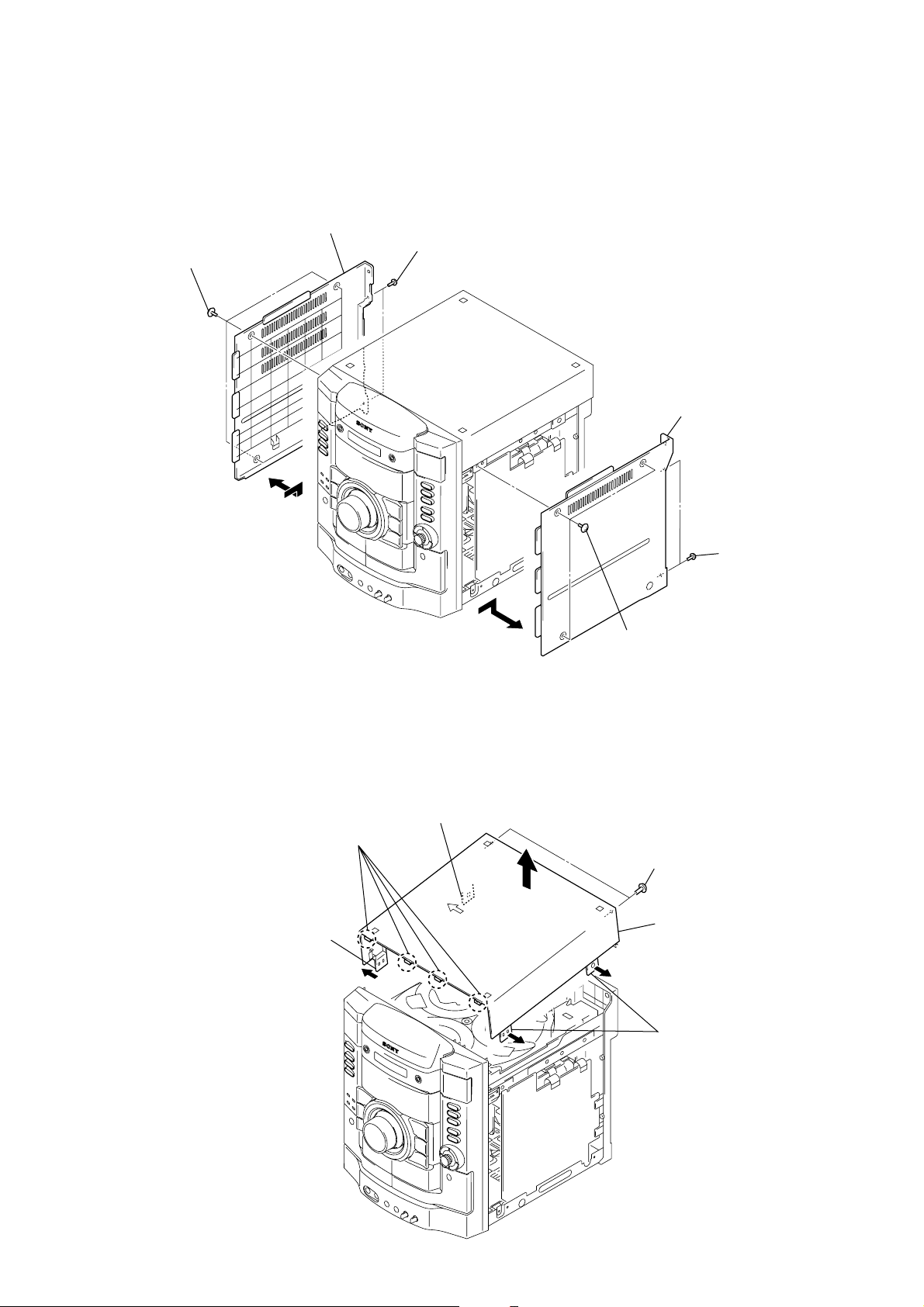
Note: Follow the disassembly procedure in the numerical order given.
s
3-2. CASE (SIDE-L), CASE (SIDE-R)
3
case (side-L)
2
two screws
1
three screws
(case 3 TP2)
(B3)
HCD-RG190/RG290
6
case (side-R)
3-3. CASE (TOP)
2
Open the case (top).
4
four claws
2
Open the case (top).
3
4
three screws
(case 3 TP2)
1
5
two screws
(B3)
case (top)
5
two screw
(B3)
2
Open the case (top).
7

HCD-RG190/RG290
)
)
3-4. LID (CD)
3
four claws
2
4
lid (CD
1
Turn the gear (loading A)
to the direction of the arrow.
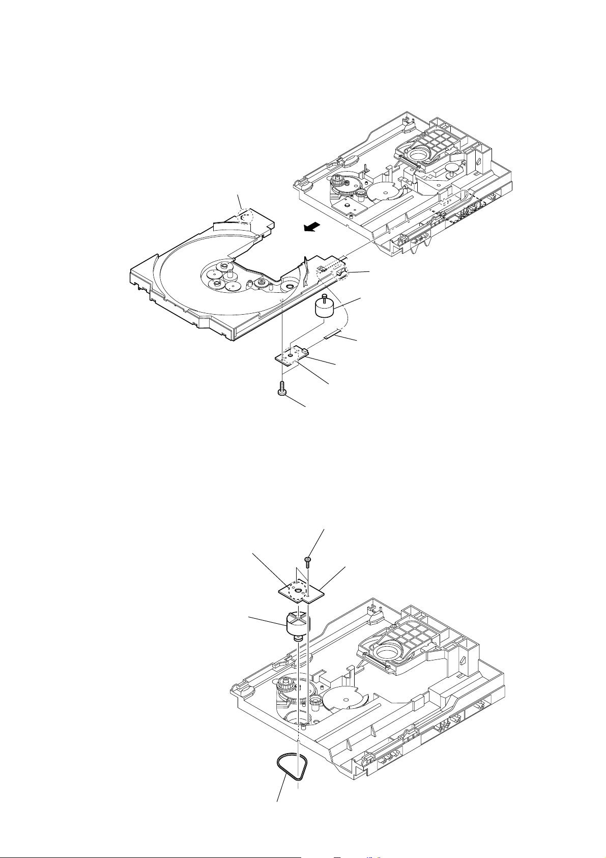
3-5. CD MECHANISM DECK
(CDM74KF-K6BD83S: EXCEPT MEXICAN MODEL)
(CDM74KF-F1BD84: MEXICAN MODEL)
3
flexible flat (13 core) cable
(Mexican model)
(CN331)
2
flexible flat (23 core) cable
(except Mexican model)
(CN301)
flexible flat (31 core) cable
(Mexican model)
(CN302)
6
CD mechanism deck
(CDM74KF-K6BD83S: except Mexican model
(CDM74KF-F1BD84: Mexican model)
4
connector
(Mexican model)
(CN1004)
1
flexible flat (13 core) cable
(CN701)
5
three screws
(BVTP3
×
8)
5
screw
(BVTP3
×
8)
5
screw (BVTP3 × 8)
8
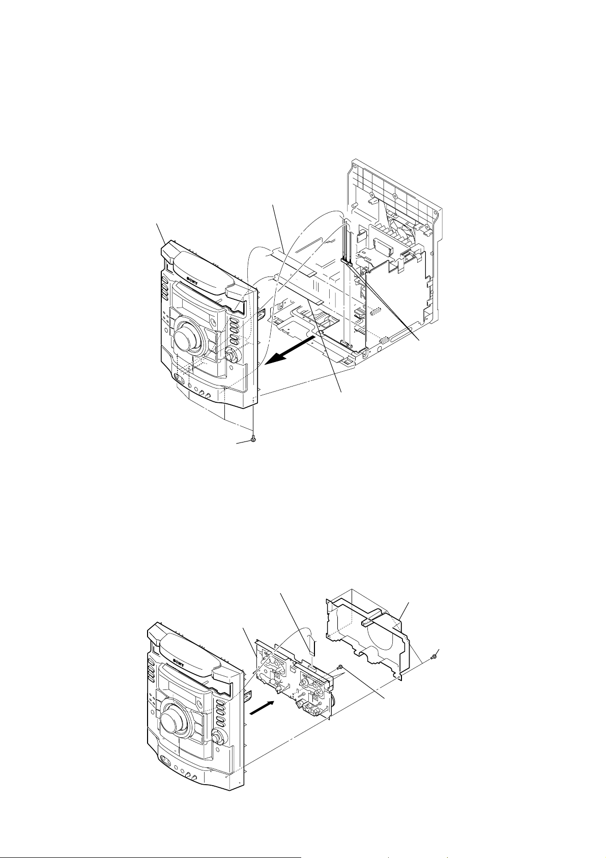
3-6. FRONT PANEL BLOCK
)
• Abbreviation
AR : Argentina model
AUS: Australian model
E2 : 120V AC area in E model
E3 : 240V AC area in E model
E51 : Chilean and Peruvian models
EA : Saudi Arabia model
MX : Mexican model
RU : Russian model
SP : Singapore model
5
front panel block
1
flexible flat cable (19 core)
(CN991)
HCD-RG190/RG290
Ver. 1.1
4
four screws
(BVTP3
×
8)
3-7. MECHA DECK (CWN42FF609)
3
flexible flat cable (11core)
5
mecha deck
(CWN42FF609)
3
two connectors
(CN301, CN302)
2
flexible flat cable (9 core)
(RG190: AEP, RU, E3, EA, SP, AUS/
RG290:AEP, UK, RU, E3, SP, AUS)
flexible flat cable (13 core)
(RG190: E2, E51, AR/RG290: E2, E51, MX, AR)
(CN061)
2
cover (TCM)
(Mexican model)
1
four screws
(BVTP2.6
4
two screws
(BVTP2.6
×
8)
×
8
9

HCD-RG190/RG290
d
Ver. 1.1
3-8. BACK PANEL SECTION
• Abbreviation
AR : Argentina model
AUS: Australian model
E2 : 120V AC area in E model
E3 : 240V AC area in E model
E51 : Chilean and Peruvian models
EA : Saudi Arabia model
MX : Mexican model
RU : Russian model
SP : Singapore model
2
connector
(CN041)
4
back panel section
1
flexible flat cable (9 core)
(RG190: RU, E2, E3, E51, EA, SP, AR, AUS/
RG290: RU, E2, E3, E51, MX, SP, AR, AUS),
flexible flat cable (11 core)
(RG190: AEP/RG290: AEP, UK)
(tuner (FM/AM))
3
two screws
(B3)
3-9. MAIN BOARD
3
connector
(CN907)
2
connector
(CN903)
3
two screws
(B3)
7
two screws
(BVTT4 × 8)
qa
6
POWER board
screw
(BV3)
0
MAIN boar
9
connector
(CN031)
10
1
flexible flat cable (11 core)
(CN008)
8
4
screw
(BVTP3 × 8)
5
screw
(BVTP3 × 8)

3-10. BD BOARD (MEXICAN MODEL), CD BOARD (EXCEPT MEXICAN MODEL)
2
screw
(BVTP2.6)
(
Mexican model
5
BD
board (
CD
board (except
1
flexible flat (16 core) cable
(CN101)
4
Remove soldering from the four points.
3
gap tube
(
Mexican model
)
HCD-RG190/RG290
)
Mexican model
),
Mexican model
)
3-11. DRIVE BOARD, SW BOARD
1
two
(BTTP (M2.6))
4
DRIVER
screws
board
CD machanism deck
(back side)
3
connector
(CN703)
5
screw
(BTTP (M2.6))
6
SW board
2
wire (flat type) (5 core)
(CN702)
CD machanism deck
(back side)
11

HCD-RG190/RG290
3-12. OPTICAL PICK-UP BLOCK
qg
optical pick-up block
2
h
older (213) assy
8
two
insulators
7
two
coil springs
(insulator)
6
two floating
(PTPWH M2.6)
qs
Remove the four solders of motor.
screws
9
1
floating
(PTPWH M2.6)
5
two
insulators
4
two
(insulator)
3
two floating
(PTPWH M2.6)
qd
flexible flat
(CN101)
qf
B
D board (
C
D board (except
qa
gap tube (Mexican model
0
s
crew (BVTP
Mexican model
(
Mexican model
2.6 × 8
)
screw
coil springs
screws
cable (16 core)
),
Mexican model
)
)
)
3-13. SENSOR BOARD
2
t
ray
1
floating
(PTPWH M2.6)
6
floating
(PTPWH M2.6)
7
g
ear (geneva)
screw
8
s
(BTTP (M2.6))
screw
crew
0
SENSOR board
9
connector
(
CN731)
3
b
elt (table)
4
floating
(PTPWH M2.6)
5
p
screw
ulley (table)
12
3-14. MOTOR (TB) BOARD
2
stopper
4
1
stopper
7
t
able motor assy (M741)
HCD-RG190/RG290
3-15. MOTOR (LD) BOARD
3
Remove the two solderings of motor.
5
l
oading motor assy (M751)
8
6
5
two
screws
(BTTP (M2.6))
2
two
(BTTP (M2.6))
3
wire (flat type) (5 core) (CN742)
MOTOR (TB) board
Remove the two solderings of motor.
screws
4
MOTOR (LD) board
1
b
elt (loading)
13

HCD-RG190/RG290
Ver. 1.1
SECTION 4
TEST MODE
COLD RESET
The cold reset clears all data including preset data stored in the
RAM to initial conditions. Execute this mode when returning the
set to the customer.
Procedure:
1. Press three buttons of s , 7 and [DISC 1] simultaneously.
2. The message “COLD RESET” is displayed on the fluorescent
indicator tube momentarily, then becomes standby states.
TUNING STEP CHANGE-OVER
(Except RG190: AEP, Russian, Saudi Arabia/
RG290: AEP, UK, Russian models)
A step of AM tuning interval can be changed over between 9 kHz
and 10 kHz.
Procedure:
1. Press the I/1 button to turn the power on.
2. Press the [TUNER/BAND] button to select “AM”.
3. Press the I/1 button to turn the power off.
4. Press two buttons of [TUNING --] and I/1 simultaneously.
5. The message “AM 9K STEP” or “AM 10K STEP” is displayed
on the fluorescent indicator tube, and thus the tuning interval
is changed over.
CD SHIP (LOCK) MODE
This mode moves the optical pick-up to the position durable to
vibration. Use this mode when returning the set to the customer
after repair.
Procedure:
1. Press the I/1 button to turn the power on.
2. Press the [CD] button to select “CD”.
3. Press two buttons of 7 and [POWER] simultaneously.
4. The message “LOCK” is displayed on the fluorescent indicator
tube, and the CD ship mode is set.
CD SHIP (LOCK) MODE & COLD RESET
This mode is used to perform CD ship (lock) mode and cold reset
simultaneously.
Procedure:
1. Press the I/1 button to turn the power on.
2. Press the [CD] button to select “CD”.
3. Press three buttons of s , [CD] and A simultaneously.
4. The message “COLD RESET” is displayed on the fluorescent
indicator tube momentarily, then becomes standby states.
ANTITHEFT LOCK MODE
This mode is used to unable to take sample disc out of disc table in
the shop.
Procedure:
1. Press the I/1 button to turn the power on.
2. Press the [CD] button to select “CD”.
3. Press two buttons of s and A for 5 seconds.
4. The message “LOCKED” is displayed on the fluorescent
indicator tube and the disc table is locked. (Even if pressing
the A button, the message “LOCKED” is displayed on the
fluorescent indicator tube and the disc table is locked)
5. To release this mode, press two buttons of s and A for 5
seconds.
6. The message “UNLOCKED” is displayed on the fluorescent
indicator tube and the disc table is unlocked.
AMP TEST MODE
This mode is used to display the parameter of amplifier IC and
display the VACS status.
Procedure:
1. Press the I/1 button to turn the power on.
2. Press three buttons of s , 7 and A simultaneously.
3. When the AMP test mode is activated, the message “AMP
TEST IN” is displayed on the fluorescent indicator tube
momentarily, then amplif ier adjustment mode is displayed on
the fluorescent indicator tube.
4. Press the [REC PAUSE/START] button to changed o ver between
VACS status display mode and the amplifier IC parameter
display mode.
5. In this mode, press the [ENTER] button to changed ov er DBFB
on/off, and “DBFB ON” or “DBFB OFF” is displayed on the
fluorescent indicator tube.
6. In this mode, press the [SURROUND] button to changed over
surround on/off, and “SURROUND ON” or “SURROUND
OFF” is displayed on the fluorescent indicator tube.
7. In this mode, press the [EQ BAND] button to enter the equalizer
adjustment mode.
In the equalizer adjustment mode, press the [EQ BAND] button
to change over the adjustment band as LO W/MID/HIGH. And
turn the multi jog knob to adjust the equalizer level of each
bands.
8. To release the amplifier IC parameter display mode or equalizer
adjustment mode, press the I/1 button to the power off.
MC TEST MODE
This mode is used to check operations of microprocessor.
Procedure:
1. Press the I/1 button to turn the power on.
2. Press three buttons of
3. When the MC test mode is activated, VACS level is displayed
on the fluorescent indicator tube momentarily.
4. Turn the multi jog knob clockwise, the message “ ALL EQ
MAX” is displayed on the fluorescent indicator tube
momentarily and turn the multi jog knob counterclockwise, the message “ALL EQ MIN” is displayed on
the fluorescent indicator tube momentarily.
5. Press the [ENTER] button, the message “ALL EQ FLAT” is
displayed on the fluorescent indicator tube momentarily.
6. Turn the [VOLUME] knob clockwise, the message “VOLUME
MAX” is displayed on the fluorescent indicator tube
momentarily and turn the [VOLUME] knob counterclockwise,
the message “VOLUME MIN” is displayed on the fluorescent
indicator tube momentarily.
7. Press the [REC PAUSE/START] button to changed over VACS
on/off.
8. Press the I/1 button to release from this mode, then cold reset
is performed.
s , 7 and [DISC 3] simultaneously.
14

HCD-RG190/RG290
VERSION DISPLAY MODE
This mode is used to check the model, destination and software
version.
Procedure:
1. Press the I/1 button to turn the power on.
2. Press three buttons of s , 7 and [DISC 2] simultaneously.
3. Fluorescent indicator tube, and LEDs are all turned on.
4. Press the [REC PAUSE/START] button to display the software
version and year, month, day of the software creation.
5. Press the [CD SYNC] button to display the model and destination.
6. To release this mode, press three buttons of s , 7 and
[DISC 2] simultaneously.
CD ERROR CODE DISPLAY MODE
This mode can be used for error code display of CD section.
Procedure:
1. Press the I/1 button to turn the power on.
2. Press the [CD] button to select “CD”.
3. Press three buttons of s , [CD] and [DISC 1] simultaneously.
4. When this mode is activated, mechanism deck error code is
displayed on the fluorescent indicator tube.
5. Press the [REC PAUSE/START] button to changed over between
optical pick-up error code display mode and mechanism deck
error code mode.
6. Turn the multi jog knob to change ov er display of error history .
7. To release this mode, press the I/1 button to turn the power
off.
1. Mechanism Deck Error Code Mode
When this mode is entered, mechanism deck error code is displayed
with the 10-character format on the fluorescent indicator tube.
The first digit from the left indicates:
The first digit from the left indicates which mode the error history
is. In the mechanism deck error code mode, “M” is displayed on
the fluorescent indicator tube.
The second digit from the left indicates:
(Error history number display)
The second digit from the left indicates which order the error history
is. “1” indicates the latest error history, and each time the number
increases by one, the error history goes back to one-previous error.
The third and 4th digit from the left indicates:
(Error status display)
The third and 4th digit from the left indicates which error status is
indicated.
The 5th and 6th digit from the left indicates:
(Present status display)
The 5th and 6th digit from the left indicates which operating status
when an error occurred is indicated.
Display Status
01 Open completion status
02 From open status, the movement to chucking down position
is under way
03 From chucking down position, the open operation is under
way
04 Chucking down completion status
10 The chucking down operation is under way
11 The chucking up operation is under way
12 Close completion status
13 From close status, the ex-open operation is under way
14 From ex-open status, the close operation is under way
18 Ex-pen completion status
The 7th and 8th digit from the left indicates:
(Motor status display)
The 7th and 8th digit from the left indicates which motor output
status when an error occurred is indicated.
Display Status
× 0 No table motor output
× 1Table motor forward output
× 2Table motor backward output
× 3Table motor break output
0 × No loading motor output
1 × Loading motor forward output
2 × Loading motor backward output
3 × Loading motor break output
The 9th and 10 th digit from the left indicates:
(Tray status display)
The 9th and 10th digit from the left indicates which target processing
when an error occurred is indicated.
Display Status
01 Open operation
12 Close operation
18 Ex-open operation
Display Status
00 No error
08 Table operation time-out (Table does not move to the tar get
position within the specified time)
16 In the chucking down operation, the operation was retried
by the maximum number of times but the operation could
not be completed
17 In the chucking up and down operation, the reverse
recovery processing was attempted but it could not be
recovered
18 In the chucking up operation, the operation was retried by
the maximum number of times but the operation could not
be completed
20 Loading operation time-out (Table does not move to the
target position within the specified time)
22 As the chuck was in the ex-open status at the initialization,
the closing was attempted but could not be completed
15

HCD-RG190/RG290
2. Optical Pick-up Error Code Mode
When this mode is entered, optical pick-up error code is displayed
with the 8-character format on the fluorescent indicator tube.
The first digit from the left indicates:
The first digit from the left indicates which mode the error history
is. In the optical pick-up error code mode, “D” is displayed on the
fluorescent indicator tube.
The second digit from the left indicates:
(Error history No. display)
The second digit from the left indicates which order the error history
is. “1” indicates the latest error history, and each time the number
increases by one, the error history goes back to one-previous error.
The third and 4th digit from the left indicates:
(Error status display)
The third and 4th digit from the left indicates which error status is
indicated.
Display Status
01 Not focused (TOC read without a disc)
02 GFS NG (TOC read with a disc chucked)
03 Start operation time-over
04 Defocused continuously (Defocused during TOC reading)
05 Q code not entered for specified time
06 Tracking not turned ON
07 Blank disc (Blank disc TOC read)
5 REPEAT LIMIT CANCEL MODE
Number of repeat for CD playback is 5 times when the repeat mode
is “REPEAT”. This mode is used to enables CD to repeat playback
for limitless times.
Procedure:
1. Press the I/1 button to turn the power on.
2. Press the [CD] button to select “CD”.
3. Press three buttons of s , [CD] and 7 simultaneously.
4. The message “LIMIT OFF” is displayed on the fluorescent
indicator tube momentarily, CD repeat 5 limit is cancelled.
CD POWER MANAGE
This mode is used to changed over CD power on/of f for decreasing
of reception noise in the tuner mode.
Procedure:
1. Press the I/1 button to turn the power on.
2. Press the [CD] button to select “CD”.
3. Press the I/1 button to turn the power off.
4. Press two buttons of s and I/1 simultaneously.
5. The message “CD POWER ON” or “CD POWER OFF” is
displayed on the fluorescent indicator tube, and CD power
on/off changed over in the tuner mode.
The 5th and 6th digit from the left indicates:
(Error step display)
The 5th and 6th digit from the left indicates which processing when
a trouble occurred
Display Contents
01 Power OFF in progress
02 Initialize in progress
03 Oscillation stopping
04 From oscillation stop, oscillation starting
05 Stopping
06 Stop operation is under way
07 Start operation in progress
08 TOC read in progress
09 Search operation is under way
0A Playback operation is under way
0B Pause operation is under way
0C Playback manual search operation is under way
0D Pause manual search operation is under way
0E —
The 7th and 8th digit from the left indicates:
The 7th and 8th digit from the left indicates which operation in
progress when a trouble occurred. (Step of each processing of the
5th and 6th digits is indicated)
16

SECTION 5
MECHANICAL ADJUSTMENTS
PRECAUTION
1. Clean the following parts with a denatured-alcohol-moistened
swab :
record/playback head pinch roller
erase head rubber belts
capstan idlers
2. Demagnetize the record/playback head with a head
demagnetizer. (Do not bring the head magnetizer close to the
erase head.)
3. Do not use a magnetized screwdriver for the adjustments.
4. After the adjustments, appiy suitable locking compound to
the parts adjusted.
5. The adjustments should be performed with the rated power
supply voltage unless otherwise noted.
TORQUE MEASUREMENT
Mode Torque Meter Meter Reading
2.6 – 6.9 mN⋅m
FWD CQ-102C (30 – 70 g⋅cm)
(0.41 – 0.97 oz⋅inch)
FWD
Back Tension
FF/REW CQ-201B 55 – 170 g⋅cm)
CQ-102C (1.5 – 6.0 g⋅cm)
0.15 – 0.59 mN⋅m
(0.021 – 0.083 oz⋅inch)
5.4 – 16.7 mN⋅m
0.76 – 2.35 oz⋅inch)
HCD-RG190/RG290
TAPE TENSION MEASUREMENT
Mode Tension Meter Meter Reading
FWD CQ-403A
more than 100 g
(more than 3.53 oz)
17
HCD-RG190/RG290
r
SECTION 6
ELECTRICAL ADJUSTMENTS
0 dB=0.775 VDECK SECTION
1. Demagnetize the record/playback head with a head
demagnetizer.
2. Do not use a magnetized screwdriver for the adjustments.
3. After the adjustments, apply suitable locking compound to the
parts adjust.
TEST TAPE
Tape Signal Used for
P-4-A063 6.3 kHz, -10 dB Azimuth Adjustment
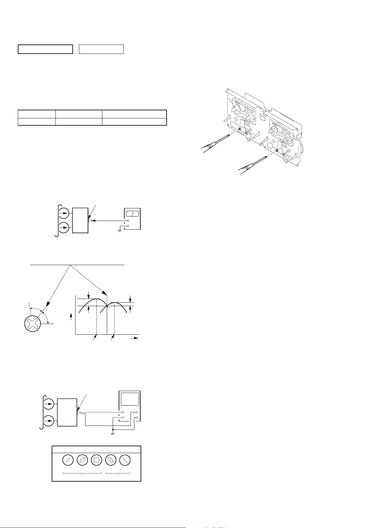
RECORD/PLA YBA CK HEAD AZIMUTH ADJUSTMENT
Note 1:Remove the mecha deck before this adjustment.
(Refer to Section 3. DISASSEMBLY (See page 6))
Note 2:Perform this adjustment for both decks.
Procedure:
1. Mode: Playback
test tape
P-4-A063
(6.3 kHz, –10 dB)
MIC. AUX. HP board
PHONES jack
(J701)
set
level mete
+
–
4. After the adjustments, apply suitable locking compound to
the pats adjusted.
Adjustment Location: Playback Head (DECK-A)
Record/Playback/Erase Head (DECK-A)
2. Turn the adjustment screw and check output peaks. If the peaks
do not match for L-CH and R-CH, turn the adjustment screw
so that outputs match within 1dB of peak.
Output
level
within
1dB
L-CH
peak
R-CH
peak
within
1dB
Screw
position
L-CH
peak
Screw
position
R-CH
peak
3. Mode: Playback
test tape
P-4-A063
(6.3 kHz, –10 dB)
MIC. AUX. HP board
PHONES jack
(J701)
set
oscilloscope
H
V
18
waveform of oscilloscope
in phase 45° 90° 135° 180°
good
wrong

HCD-RG190/RG290
e
V
TP
(VC)
TP
(RFACI)
IC201
– BD Board (Conductor Side) (RG290: MX) –
CD SECTION
Note:
1. CD Block is basically constructed to operate without adjustment.
2. Use YEDS-18 disc (3-702-101-01) unless otherwise indicated.
3. Use an oscilloscope with more than 10 MΩ impedance.
4. Clean the object lens by an applicator with neutral detergent when the
signal level is low than specified value with the following checks.
5. Check the focus bias check when optical pick-up block is replaced.
• Abbreviation
MX: Mexican model
FOCUS BIAS CHECK
oscilloscop
CD board (Except RG290: MX)
BD board (RG290: MX)
TP (RFACI)
TP (VC)
Procedure :
1. Connect oscilloscope to TP (RF ACI) and TP (VC) on the CD
board (Except RG290: MX) or BD board (RG290: MX).
2. Press the I/1 button to turn the power on, and press
the A button to open the CD disc table.
3. Set disc (YEDS-18) on the tray and press the 7 button to
playback.
4. Confirm that oscilloscope waveform is as sho wn in the figure
below. (eye pattern)
A good eye pattern means that the diamond shape (◊) in the
center of the waveform can be clearly distinguished.
(DC range)
+
–
Connecting Location:
– CD Board (Conductor Side) (Except RG290: MX) –
TP
(VC)
IC201
TP
(RFACI)
VOLT/DIV: 200 m
TIME/DIV: 500 ns
level:
0.9 ± 0.4 Vp-p
19

HCD-RG190/RG290
MEMO
20
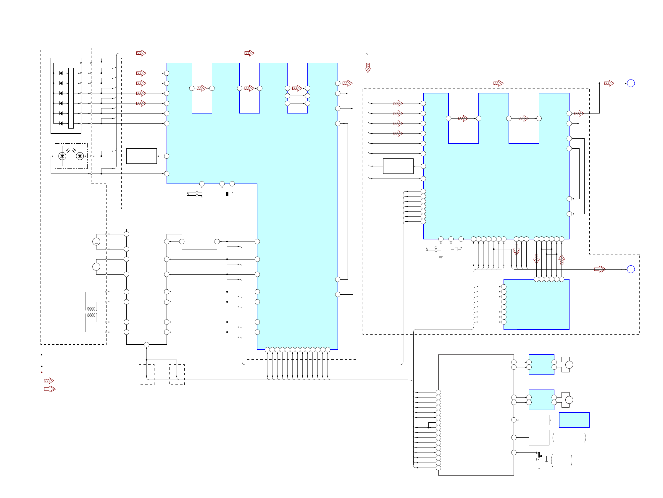
SECTION 7
DIAGRAMS
7-1. BLOCK DIAGRAM – CD SERVO Section –
+3.3VDETECTOR
HCD-RG190/RG290
A
B
C
D
E
F
LASER DIODE
PD
OPTICAL PICK-UP BLOCK
(KSM-213DCP)
(EXCEPT RG290: MX)
(KSM-215DCP)
(RG290: MX)
(EXCEPT RG290: MX)
(EXCEPT RG290: MX)
Abbrivation
: Mexican modelMX
R-ch is omitted due to same as L-ch.
SIGNAL PATH
: CD PLAY
: VIDEO
HCD-RG190/RG290
I-V AMP
LD
M401
M101
(RG290: MX)
(SPINDLE)
M402
M102
(RG290: MX)
(SLED)
2-AXIS
DEVICE
(TRACKING)(FOCUS)
A
A
B
C
D
E
F
LD
PD
AUTOMATIC
POWER CONTROL
Q321
(EXCEPT RG290: MX)
16 CH4OUTF
M
15 CH4OUTR
17 CH3OUTF
M
18 CH3OUTR
14 CH1OUTF
13 CH1OUTR
12 CH2OUTF
CH2OUTR
11 7
MUTE
20
C-4
57
58 B
AC_
SUM
59 C
60 D
50 E
51 F
66 LD
67 PD
S201
(LIMIT)
FOCUS/TRACKING COIL DRIVE,
SPINDLE/SLED MOTOR DRIVE
IC402 (EXCEPT RG290: MX)
IC251 (RG290: MX)
27 OPOUT 38 MDP
24
CH4IN
23
CH3FIN
22
CH3RIN
4
CH1FIN
5
CH1RIN
6
CH2FIN
CH2RIN
C-8
(RG290: MX)(EXCEPT RG290: MX)
CD-L
SBSO, WFCK,
SCOR, EXCK
A
(Page 22)
B
(Page 23)
C-1
8
C-8
112AOUT1
R-CH
117AOUT2
A
55FEO
53TEO
52TEI
54FEI
B
C
D
E
F
LD
PD
(RG290: MX)
AUTOMATIC
POWER CONTROL
Q10
MDP
SFDR
SRDR
TFDR
TRDR
FFDR
FRDR
S101
(LIMIT)
C-3
C-5
C-15
C-4
C-6
C-7
C-11
C-12
C-9
C-10
C-14
C-13
C-1
C-8
MP3-RST
A
26
27 B
28 C
29 D
19 E
20 F
36 LD
37 PD
6 MDP
9 SFDR
10 SRDR
11 TFDR
12 TRDR
13 FFDR
14 FRDR
AC_
34
SUM
SSTP
7
52
O-CD-DATA
54
O-CD-CLK
28
O-XLAT/O-MP3-STB
31
O-D-MUTE/O-XLT
53
I-CD-SENS
40
I-SCOR
71
I-MP3-DATA
72
O-MP3-DATA
70
O-MP3-CLK
26
O-MP3-XLAT/O-MP3-CS
30
O-MP3-CS/O-MP3-LP
29
I-MP3-REQ
27
I-MP3-ACK
24
O-XTCN
32
O-XRST
25
O-MP3-RESST
XTAO
XTAI
77
78
X171
16.9344MHz
SYSTEM CONTROLLER
IC901 (1/4) (EXCEPT RG290: MX)
IC901 (1/4) (RG290: MX)
EG_
35
IN
DATA
CLOK
XLAT
105102
104
107
C-3
C-5
C-4
C-6
C-11
C-12
C-9
C-13
C-14
C-10
MP3-RST
C-15
I-CD-NUMBER-SENS
I-CD-ENCODER
41RFACO 42 RFACI
CD DSP
IC101
SENS
SCOR
XTACN
XRST98SBSO
115
95
110
C-1
C-8
C-7
SCOR
6MIDIO
7MICK
4MICS
8MIACK
36 PO11/BUCK/AD14
5MILP
2RESET
3 STANDBY
34
O-LM-F
33
O-LM-R
36
O-TM-F
35
O-TM-R
37
66
I-OPEN-SW
38
EXCK
WFCK
65
99
110
EXCK
WFCK
SBSO
15
LOADING MOTOR DRIVE
7
FIN
9
RIN
TABLE MOTOR DRIVE
7
FIN
9
RIN
LEVEL SHIFT
Q731
ROTARY
ENCODER
S711
OPEN
CLOSE
PCMD
BCK63LRCK60BCKI65LRCKI61PCMDI
66
54
28
19
18
SDIO
BCKA
LRCKA
SBSY/BCKIB
MP3 DECODR
IC301
IC701
4
OUT1
2
OUT2
IC712
4
OUT1
2
OUT2
ADDRESS DETECT
DISC TABLE
OPEN/CLOSE
DETECT
81AOUT1
86AOUT2
24FEO
22TEO
21TEI
23FEI
71
SDO0
SFSY/LRCKIB
M751
M
(LOADING)
M741
M
(TABLE)
DISC TABLE
ADDRESS SENSOR
IC731
DISC TABLE
S751
R-CH
39
OPIN+
65
EG_
IN
XTAI
109
X201
16.9344MHz
2
70RFACO 71 RFACI 3PCMD
CD DSP
IC201
XTAO
108
MDP
SFDR
SRDR
TFDR
TRDR
FFDR
FRDR
41 SFDR
42 SRDR
43 TFDR
44 TRDR
45 FFDR
46 FRDR
4 PCMDI
5BCK
1LRCK 2 LRCKI
DATA
CLOK11XLAT16SENS20SCOR26DATA212CLK290XLAT-MP313REQ-MP314IREQ-MP310ACK-MP315XTACN7XRST
89
C-3
C-5
C-15
C-6
C-7
C-11
C-12
C-9
6 BCKI
C-10
C-14
C-13
64
SSTP
+3.3V
2121

HCD-RG190/RG290
Ver. 1.1
7-2. BLOCK DIAGRAM – MAIN Section –
(Page 23)
(Page 21)
(RG290: MX)
JK801
MIC 1
JK802
MIC 2
JK802
MIC
RG190: E2, E51, AR/
RG290: E2, E51,AR
HP IN
C
J702
AUDIO IN
CD-L
A
HP1
(PB)
(DECK-A)
L-CH
R-CH
+9V
RG190: E2, E51, AR/
RG290: E2, E51, MX, AR
R-CH
R-CH
RG190: E2, E51, AR/
RG290: E2, E51, AR
MUTING
Q801
PB SWITCH
(DECK-A)
Q301
R-CH
DIGITAL
ECHO
IC802
MIC AMP
IC801 (1/2)
+
(RG290: MX)
VR851
ECHO LEVEL
VR801
MIC LEVEL
RG190: E2, E51, AR/
RG290: E2, E51, MX, AR
MIC AMP
IC801 (2/2)
PB AMP
IC301
INPUT SELECTOR, TONE CONTROL,
ELECTRICAL VOLUME
IC101 (EXCEPT RG290: MX)
36
MIC137MIC2
2 10
AUXL 11 VINLTONEOUTL 14OUTL
40 CDL
39 TAPEL
1 TUNERL
IC101 (RG290: MX)
3RECOUTL
Abbrivation
: Argentina modelAR
: 120V AC area in E modelE2
: Chilean and Peruvian modelsE51
: Mexican modelMX
R-ch is omitted due to same as L-ch.
SIGNAL PATH
: TUER (FM/AM)
: CD PLAY
: TAPE PLAY (DECK-A)
: TAPE PLAY (DECK-B)
: REC
: MIC
: AUDIO IN
OUT
E
(Page 23)
R-CH
13BB22
BASS AGC
Q113
D031
BASS AGC
F
(Page 23)
HRPE1
(REC/PB/ERASE)
(DECK-B)
ERASE
FM75Ω
COAXIAL
AM
L-CH
R-CH
ANTENNA
R-CH
FM ANT
AM ANT
MUTING
Q305
MUTING
MUTING
Q307
Q401
L451
BIAS OSC
TUNER (FM/AM)
TUNER-L
TUNER-R
PLL DO
PLL CLK
PLL CE
RDS DATA
RDS CLK
BIAS OSC
Q453
PLL DI
R-CH
R-CH
REC BIAS
Q451, 452
R-CH
PB SWITCH
(DECK-B)
MUTING CONTROL
CONTROL SWITCH
Q305, 306
Q400, 407
SWITCH
Q303
R-CH
MUTING
SWITCH
+9V
SELECT SWITCH,
SELECT SWITCH
4
O-BIAS
45 I-LC23003-DI
43 O-LC23003-DO
44 O-LC23003-CLK
42 O-LC23003-CE
DECK-A/B
REC/PB
Q405, 406, 408
2
O-REC/PB
REC SWITCH
Q403
R-CH
REC CONTROL
SWITCH
Q409, 410
3
O-REC-MUTE
55
61
I-MIC-DET
I-HP/AUDIO IN
REC AMP
IC401
DATA15CLK
16
58
57
O-R2S15207FP-DATA
SYSTEM CONTROLLER
IC901 (2/4) (EXCEPT RG290: MX)
IC901 (2/4) (RG290: MX)
O-AUDIO-CLK
SAOUT
4
BAND-PASS
FILTER
Q111, 112
D923 D921
68
63
I-VACS
I-STREAM
I-TCM-SYNC
73 36
TAPE MECHANISM
DECK CONTROLLER
IC701 (1/2)
O-TCM-SYNC
O-MOTOR
O-SOL-A
O-SOL-B
I-HALF-A
I-HALF-B
I-RELL-A
I-RELL-B
I-REC-SW
33
34
35
30
27
31
28
29
CAPSTAN/REEL
MOTOR DRIVE
Q701, 704
TRIGGER PLUNGER
DRIVE (DECK-A)
Q703, 706
TRIGGER PLUNGER
DRIVE (DECK-B)
Q702, 705
TAPE MECHANISM
DECK BLOCK
CAMP+
M
A-SOL
B-SOL
A-HALF
B-HALF
A-PHOTO
B-PHOTO
B-REC-F
HCD-RG190/RG290
(Page 23)
D
RDS-DATA, RDS-CLK
RDS-DATA
(RG190: AEP/RG290: AEP, UK)
RDS-CLK
2222

7-3. BLOCK DIAGRAM – AMP/VIDEO Section –
BASS AGC
F
(Page 22)
E
(Page 22)
OUT
IC251 (EXCEPT RG290: MX)
IC251 (RG290: MX)
BUFFER
MUTING
Q251
R-CH
IC441 (RG190)
IC441 (RG290)
POWER AMP
STANDBY SWITCH
Q489
+
TH441
R-CH
R-CH
HCD-RG190/RG290
Ver. 1.1
HP IN
C
(Page 22)
J701
R-CH
–1
JK441
+
–
–2
–
+
RY441
RELAY B+
PHONES
L
SPEAKER
R
(RG290: MX)
SBSO, WFCK,
SCOR, EXCK
B
(Page 21)
MUTING
CONTROL SWITCH
Q261
21
SBSO
WFCK
SCOR
EXCK
D-RAM
IC1002
O-SYS-XMUTE
SCHMITT
TRIGGER
IC1005
DQ1 – DQ4
A0 – A7
WE
OE
RAS
CAS
5
O-STK-MUTE
1, 2, 24, 25
9 – 12, 14 – 17
R-CH
SYSTEM CONTROLLER
IC901 (3/4) (EXCEPT RG290: MX)
IC901 (3/4) (RG290: MX)
CD GRAPHICS DECODER
IC1001
3 44
DATA
5
SFSY
4
SBSY
2
CLCK
VD0 – VD3
25, 27, 29, 30
VA0 – VA7
15 – 22
133
XWE
2822
XOE
144
XRAS
2623
XCAS
VOUT
GDET
MUTE
XRESET
DEN
XO1
XI1
60
59
OVER LOAD
DETECT
Q441
+
37
6
54
52
DC DETECT
Q481, 482
VIDEO AMP
IC1006
VIDEO MUTING
Q1010
LEVEL SHIFT
Q1005, 1009
LEVEL SHIFT
Q1002, 1006
NTSC/PAL
SELECT SWITCH
Q1001
TEMPERATURE
DETECT
Q483, 484
+
+
RG290: AEP, UK, MX
I-CDG-DET
O-VMUTE
48
46
PROTECTOR
Q485
RG190: AEP/
O-CDG-MUTE-DATA
/I-RDS-DATA
O-CDG-RST
/I-RDS-CLK
49
41
R-CH
D035
RELAY DRIVE
Q486, 488
PROTECT
DETECT
Q487
+
64
I-PROTECTOR
FAN MOTOR
DRIVE
Q043 – 045
FAN MOTOR
DETECT
Q046
J803
M
VIDEO OUT
M001
(FAN)
PROTECT
G
(Page 24)
(Page 22)
RDS-DATA
RDS-CLK
RDS-DATA, RDS-CLK
(RG190: AEP/RG290: AEP, UK)
D
Abbrivation
: Mexican modelMX
R-ch is omitted due to same as L-ch.
SIGNAL PATH
+3.3V
: TUNER (FM/AM)
: VIDEO
HCD-RG190/RG290
X102
14.31818MHz
2323

HCD-RG190/RG290
Ver. 1.1
7-4. BLOCK DIAGRAM – PANEL/POWER SUPPLY Section –
D601 – 605
(STREAM)
FL701
FLUORESCENT
INDICATOR
TUBE
S611 – 613,
S621 – 627,
S631 – 638,
S671
VOLUME
S672
(MULTI JOG)
LED DRIVE
Q601 – 605
ROTARY
ENCODER
ROTARY
ENCODER
FLUORESCENT INDICATOR TUBE
/LED DRIVER
IC701 (2/2)
SO1
XRESET
X2
X1
4
3
X701
4.19MHz
D611
STANDBY
REMOTE CONTROL
RECEIVER
SI1
SCK1
CE
IC610
S1 – S21
61 – 67
45 – 58,
G1 – G13
68 – 80
STREAM LED1
– STREAM LED5
39 – 43 19 – 21
KEY1 – KEY3
10 I-VOL-A
11 I-VOL-B
12 I-JOG-A
13
I-JOG-B
S601 – 606
SYSTEM CONTROLLER
IC901 (4/4) (EXCEPT RG290: MX)
IC901 (4/4) (RG290: MX)
I-VFD-DATA9 77
O-VFD-DATA8 76
O-VFD-CLK7 78
O-VFD-CE16 75
O-VFD-RESET6 74
69 O-STBY-LED
80 I-XSIRCS-IN
65 I-KEY0
79 I-WAKEUP
X2 (16MHZ)
X1 (16MHZ)
14
15
16MHz
X902
12
32.768kHz
23O-FRONT-SP-RELAY
47O-CDG-POWER
10I-XRESET
9I-AC-CUT
1I-AC-PULSE
7O-POWER-RELAY
XT2 (32.768KHZ)
XT1 (32.768KHZ)
11
X901
RESET SWITCH
Q901
RELAY B+
CDG +5V
M+7V
M+9V
+9V
UNREG +16V
+3.3V
CD DSP +1.8V
MP3 +1.5V
+5V
REGULATOR
IC1003
+1.8V
REGULATOR
IC203
(EXCEPT RG290: MX)
+1.5V
REGULATOR
IC303
(RG290: MX)
IC902 (EXCEPT RG290: MX)
B+ SWITCH
Q041, 042
(RG290: MX)
B+ SWITCH
Q1007, 1008
D301, 302
D001
VDD (+3.3V)
RESET SIGNAL
GENERATOR
IC902 (RG290: MX)
+9V
REGULATOR
IC021 (EXCEPT RG290: MX)
IC021 (RG290: MX)
+9V
REGULATOR
IC011 (EXCEPT RG290: MX)
IC011 (RG290: MX)
+3.3V
REGULATOR
IC006 (EXCEPT RG290: MX)
IC006 (RG290: MX)
D008
D007
D902
EVER +10V
PROTECT
DETECT
Q011
REGULATOR
Q903, 904
AC DETECT
Q902
D021 – 024
D011 – 014
D001 – 004
D006
D902 – 905
RECT
RECT
RECT
RECT
RECT
D910
VF
VF
–VFL
SECTION
AMP
B+
–27V
REGULATOR
Q902
RECT
D401
F907
F906
MAIN POWER
TRANSFORMER
D908
F904
F905
SUB POWER
TRANSFORMER
PT901
RG190: AEP, RU, AR, AUS/
RG290: AEP, UK, RU, MX, AR, AUS
RG190: E2, E3, E51, EA, SP
/RG290: E2, E3, E51, EA
RG190: AEP, RU, AR, AUS/
RG290: AEP, UK, RU, MX, AR, AUS
PT902
Abbrivation
VOLTAGE
SELECTOR
: Argentina modelAR
: Australian modelAUS
: 120V AC area in E modelE2
: 240V AC area in E modelE3
: Chilean and Peruvian modelsE51
: Saudi Arabia modelEA
: Mexican modelMX
: Russian modelRU
: Singapore modelSP
S901
RY901
POWER ON/OFF
RELAY DRIVE
Q002
(AC IN)
PROTECT
G
(Page 23)
HCD-RG190/RG290
2424

HCD-RG190/RG290
)
Ver. 1.1
• Note For Printed Wiring Boards and Schematic Diagrams
Note on Printed Wiring Board:
• X : parts extracted from the component side.
• Y : parts extracted from the conductor side.
• f : internal component.
• : Pattern from the side which enables seeing.
(The other layers' patterns are not indicated.)
Caution:
Pattern face side: Parts on the pattern face side seen from
(Conductor Side) the pattern face are indicated.
Parts face side: P arts on the parts face side seen from
(Component Side) the parts face are indicated.
Caution:
Pattern face side: Parts on the pattern face side seen from
(Side B) the pattern face are indicated.
Parts face side: P arts on the parts face side seen from
(Side A) the parts face are indicated.
• Indication of transistor
C
Q
B
E
B
These are omitted.
Q
CE
These are omitted.
Note on Schematic Diagram:
• All capacitors are in µF unless otherwise noted. (p: pF)
50 WV or less are not indicated except for electrolytics
and tantalums.
• All resistors are in Ω and 1/
specified.
• f : internal component.
• 2 : nonflammable resistor.
• 5 : fusible resistor.
• C : panel designation.
Note: The components identified by mark 0 or dotted line
with mark 0 are critical for safety.
Replace only with part number specified.
• A : B+ Line.
• B : B– Line.
• Voltages and wavefor ms are dc with respect to ground
under no-signal (detuned) conditions.
– CD/BD Boards –
no mark :CD PLAY
– CD-G Board –
no mark : CD-G PLAY
– Other Boards –
no mark : TUNER (FM/AM)
(): CD PLAY
〈〈 〉〉 : TAPE PLAY
{ }: TAPE REC
∗ : Impossible to measure
• Voltages are taken with a V OM (Input impedance 10 MΩ).
Voltage variations may be noted due to normal production tolerances.
• Waveforms are taken with a oscilloscope.
Voltage variations may be noted due to normal production tolerances.
• Circled numbers refer to waveforms.
• Signal path.
F : TUNER (FM/AM)
J : CD PLAY
E : TAPE PLAY (DECK-A)
d : TAPE PLAY (DECK-B)
G : REC
N : MIC
f : AUDIO IN
L : VIDEO
• Abbreviation
AR : Argentina model
AUS: Australian model
E2 : 120 V AC area in E model
E3 : 240 V AC area in E model
E51 : Chilean and Peruvian models
EA : Saudi Arabia model
MX : Mexican model
RU : Russian model
SP : Singapore model
4
W or less unless otherwise
• Circuit Boards Location
KEY LEFT board
PANEL board
MIC. AUX. HP board
TRANSFORMER board
MOTOR (LD) board
VIDEO-OUT board
(MX model)
CD-G board
(MX model)
SW board
BD board (MX model)/
CD board (EXCEPT MX model)
SENSOR board
DRIVER board
TUNER (FM/AM
MOTOR (TB) board
KEY RIGHT board
MAIN board
HCD-RG190/RG290
POWER board
DECK board
• Abbreviation
MX : Mexican model
2525
HCD-RG190/RG290
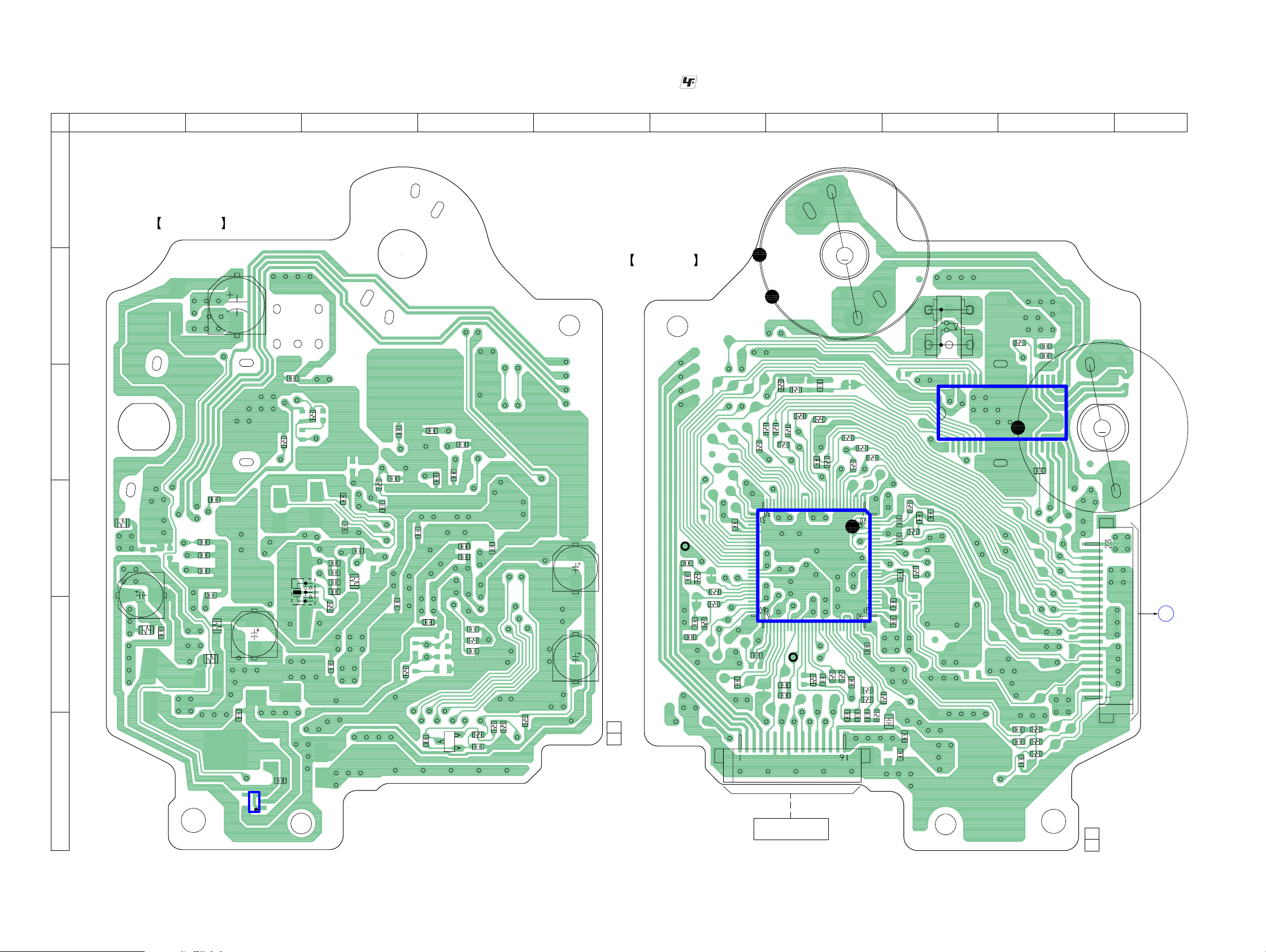
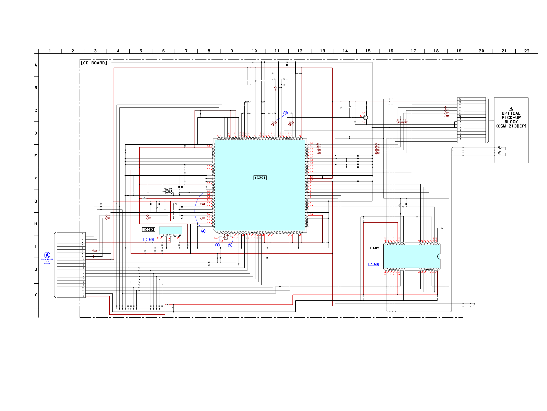
7-5. PRINTED WIRING BOARD – CD Board (Except RG290: MX model) –
1 2 3 4 567 8 9 10
A
CD BOARD
(COMPONENT SIDE)
C401
B
C406
C226
X201
C204
R421
C277
C276
C268
R271
C275
C267
C266
C272
R276
C219
C215
R203
C223
R260
C
D
E
F
R401
C201
R201
C202
R202
R207
C101
C102
C108
C424
C110
C227
R423
C203
3
4
1
5
IC203
C104
C271
C105
C220
C210
C321
• See page 25 for Circuit Boards Location.
C109
C107
C232
C206
C257
R256
C274
E
Q321
R323
C322
C205
R322
R321
R324
C207
C323
1-868-067-
12
(12)
: Uses unleaded solder.
CD BOARD
(CONDUCTOR SIDE)
C224
TP
(VC)
C251
C253
R252
R253
R255
R254
C256
C252
C254
R102
R101
31
60
M401
(SPINDLE)
R452
R451
R104
R107
R109
R108
30
IC201
61
C208
C258
C230
OPTICAL PICK-UP BLOCK
TP
(RFACI)
CN301
(KSM-213DCP)
C103
R257
C451
R110
C260
R105
R103
R250
M
C264
R278
C261
R258
R265
C221
R268
C273
S201
(LIMIT)
28 22
R280
C405
21 15
C403
IC402
17 14
R277
R275
1
120
91
90
C265
R266
C217
C303
R267
C218
C214
C213
C222
C304
R292
C301
R291
R270
C291
C292
C112
C113
C111
8
C404
R112
R113
R111
1-868-067-
M
M402
(SLED)
CN102
A
12
(12)
MAIN
BOARD
CN301
(Page 34)
HCD-RG190/RG290
2626
HCD-RG190/RG290
7-6. SCHEMATIC DIAGRAM – CD Board (Except RG290: MX model) –
0.1
C222
0.1
C213
C214
0.1
C223
0.1
C266C267
10p5p
R270
1k
R271
1M
1
C276
R291
100
C291
470p
1
C277
C292
470p
R292
100
C219
0.1
VOUT
NC
C220
C227
1
0.1
C401
220
10V
(Page
37)
DATA
CLK-MP3
D-MUTE
DVDD(3.3V)
D-OUT
D-GND
L-CH
A-GND
R-CH
AVDD(3.3V)
XATCN
XRST
IREQ-MP3
CLK
DATA-MP3
XLAT-MP3
REQ-MP3
ACK-MP3
XLAT
SENS
SCOR
M-GND
M+7V
+1.8V REGULATOR
BH18LB1WG-TR
R110
R103
R105
R104
R109
R108
R107
R102
R101
IC203
100
100
100
100
100
100
100
100
100
16.9344MHz
C218
0.1
C201
100
10V
R207 C226
01
22p
22p
C105
C103
X201
C202
0.1
C217
0.1
GND
STBY
VIN
C203
C204
100
0.1
10V
220p
220p
220p
R401
0
107
C
C109
C104
C268 C215
C275
10p 0.1
5p
100
R113
100
R112
R111
100
CN102
23P
R201
0
22p
22p
C112
C113
R203
R202
0
22p
22p
220p
220p
220p
C101
C102
C110
C108
C111
• See page 53 for Waveforms. • See page 58 for IC Block Diagrams. • See page 62 for IC Pin Function Description.
C210
0.1
0
C264
R260
C273
4.7k
0.1
C265
R265
R266
1k
10k
R267
4.7k
C221
0.1
R275
100
CLK2
SVSS
SVDD
JTAGTCK
JTAGTDI
JTAGTDO
JTAGTMS
TRST
VSS
VDD
IOVDD2
DOUT
TEST
TES1
IOVSS2
PLLVDD
PLLVSS
XVSS
XTAO
XTAI
XVDD
AVDD1
AOUT1
VREFL
AVSS1
AVSS2
VREFR
AOUT2
AVDD2
IOVDD0
R276 C271
47k 0.1
100
R277
VDD
VSS
DATA
TEST1
SSTB-MP3
PCMDI
BCK
PCMD
BCKI
LRCKI
LRCK
IOVSS0
R268
FILI
PCO
FILO
SVSS
SVDD
VSS
XRST
XTACN
100
R278
IREQ-MP3
VPCO
VCTL
CLTV
AVSS3
CD DSP
IC201
CXD3014A-201R
CLOK
DATA2
XLAT-MP3
ACK-MP3
REQ-MP3
C230
100p
C260
C261
1M
R250
220p
220k
R257
100k
C258
R258
RFC
BIAS
ASYI
ASYO
RFACI
AVSS4
RFACO
AVDD3
SVDD
SVSS
VDD
XLAT
C272
0.1
XPCK
XUGF
WFCK
SENS
R280
0
TP
(RFACI)
0.47
0.01
1000p
470p
C208
0.1
R256
22k
C257
0.1
C274
0.1
C301
0.1
R321
C323
R324
100
100k
C256
0.1
LD
PD
C2PO
GFS
D
EG_IN
AVDD4
RFDCO
C
PDSENS
AC_SUM
B
A
VC
FEO
FEI
TEO
TEI
F
E
AVSS0
AVDD0
IOVDD1
FRDR
FFDR
TRDR
TFDR
SRDR
SFDR
IOVSS1
SSTP
MDP
LOCK
VSS
VDD
VSS
FOK
DFCT
MIRR
SVDD
SVSS
COUT
SCOR
VDD
C206
0.1
C224
0.1
10V
R255
1k
R253
1k
2.2
C322
1
R322
2.2
100 10V
4700p
470p
4700p
470p
C404
0.1
C405
C232
0.1
FOCUS/TRUCKING
SPINDLE/SLED
MOTOR DRIVE
0.1
COIL DRIVE,
IC402
BA5947FM
2SA2119K
AUTOMATIC
POWER
CONTROL
Q321
R323
0
C321
1000p
TP
(VC)
C207
C254
C253
R254
10k
C252
C251
R252
10k
C205
0.1
C304
C303
1
10
R452 C451
10k 0.047
R451
22k
C424
0.1
R423
10k
GND
CNF4
POWVCC
CH2OUTF
CH10UTF
CH2OUTR
CH1OUTR
GND
MUTE
POWVCC
CH3OUTR
CH3OUTF
CH4OUTF
CH4OUTR
P-
L+
SL-
S
S
SP+
CH2RIN
CH3RIN
OPIN-
OPIN+
CH1FIN
CH2FIN
CH1RIN
GAIN-SW
POUT
PREVCC
VREF
O
CH4CAPA
CH4IN
CH3FIN
C406
CN301
16P
VC
VCC
E
D
A
B
C
F
GND
LD
VR
PD
F+
T+
T-
F-
SP+
SP-
SL+
SL-
R421
0
0.1
S201
(LIMIT)
(SPINDLE)
M401
M402
(SLED)
HCD-RG190/RG290
2727

HCD-RG190/RG290
7-7. PRINTED WIRING BOARD – BD Board (RG290: MX model) –
1 2 3 4 567 8 9 10 11
A
BD BOARD
(COMPONENT SIDE)
C302
B
C209
C151
C210
C315
C316
C318
R165
C305
X171
C314
R162
R313
R171
C312
C174
C172
R191
R172
R173
C171
C134
R302
C308
C196
C195
C125
R121
C123
C303
C
D
FB301
R205
R201
C201
C184
C183
C182
E
C203
F
• See page 25 for Circuit Boards Location.
C255
C260
C257
R253
C116
C17
1-864-566-
C15
C10
C11
C16
C258
C259
Q10
C18
C14
R12
R11
R13
R10
E
: Uses unleaded solder.
BD BOARD
(CONDUCTOR SIDE)
C252
28 22
IC251
17 14
R251
11
(11)
R252
C251
M101
(SPINDLE)
21 15
C114
C113
8
TP
(VC)
R113
C112
C111
R114
R112
CN101
OPTICAL PICK-UP BLOCK
(KSM-215DCP)
R111
M
S101
(LIMIT)
IC301
R407
IC101
C124
R132
R404
48
C310
C133
R131
R351
C306
R353
R354
R352
C307
C320
C115
17
R307
32
C309
R411
33
R303
120 91
1
32
30
31
C122
TP
(RFACI)
116
R419
C132
64
49
R163
C163
R133
C131
IC303
13
5
4
R405
R403
C313
C141
R408
C213
C194
C181
R151
R203
1-864-566-
R301
R306
C311
R410
R409
C211
C212
R406
R412
90
C162
C161
61
60
C143
R141
R142
R143
C142
C317
R305
R402
R401
R182
R161
M
M102
(SLED)
1
CN201
B
MAIN
BOARD
CN302
(Page
38)
C186
C185
R181
R204
31
R422
R421
R423
11
(11)
HCD-RG190/RG290
2828

HCD-RG190/RG290
7-8. SCHEMATIC DIAGRAM – BD Board (RG290: MX model) –
C307
R307
0.1
10k
VDD
IRQ/FIO
VSSX
BH15FB1WG
SDI1/
DATA
TXO
LRCKIA
BCKIA
SBSY/BCKIB
SFSY/LRCKIB
SDI0
LRCKO
BCKO
SDO0
VSS
VDDT
MIACK
MICK
MIDIO
MILP
MICS
STANBY
RESET
VDDP
VCOI
VSSP
MIMD
TEST
R313
220
C316C315
0.00220.1
IC303
MP3STB
MP3REQ
MIACK
MICK
MIDIO
MILP
MICS
MP3RST
R411
SCOR
100
R410
100
R409
100
R408
100
R407
100
R406
100
R412
100
100
R423
100
R421
100
R422
XTACN
CLOCK
C212
SENS
22p
XLT
C211
DATA
220p
XRST
AOUT1
WFCK
SBSO
EXCK
AOUT2
C306
R405
R404
R419
R403
R402
R401
R301
100k
R305
100k
C317
0.01
DOUT
MP3REQ
R303
100k
C310
0.1
(Page 41)
FB301
WE/SDO1
SDO2
CS/RAS/
PO12
AD15/CAS/
PIO7/BUS3/IO7
SDO3/OE
PO9/AD12
PO08/AD11
VDDM
SRMSTB
VDDT
AD10
AD9
AD8
PO07/AD7
PO06
/AD6
PO05
/AD5
C314
47
4V
CN201
31P
M+7V
M-GND
M-GND
MP3-STB
MP3-REQ
MP3-ACK
MP3-CLK
MP3-DIO
MP3-LP
MP3-CS
MP3(3.3V)
MP3-RST
MP3-GND
SCOR
CD-SENS
CD-CLK
XLT
CD-DATA
XRST
XTCN
AVDD(3.3V)
R-CH
A-GND
L-CH
D-GND
D-OUT
DVDD(3.3V)
D-GND
WFCK
SBSO
EXCK
PIO6/FI3/BUS2/IO7
PIO5/FI2/BUS1/IO5
PIO4/FI1/BUS0/IO4
PO11/BUCK/AD14
PO10/CCE/AD13
AD0/PO00
AD1/PO01
AD3/PO03
AD2/PO02
AD4/PO04
C312C313
C311 C309
0.10.1
0.1 0.1
VOUT
C305
C302 C303
220
0.1 0.1
4V
R205
R204
PIO3/IO3
PIO2/IO2
MP3 DECODER
TC94A34FG-002
VDD
VSS
C308
47
4V
STBY
NC
0
0
PIO0/SDI2/IO0
PIO1/SDI3/IO1
IC301
VDDX
CKO/PO13/AD16
VIN
GND
R306
VSS
XO
0
CKI/CLOCK/
XI
+1.5V REGULATOR
• See page 53 for Waveforms. • See page 58 for IC Block Diagrams. • See page 62 for IC Pin Function Description.
100p
C142
1500p
R203
0
R354
100
R352
R351
100
0.1
100
MIACK
100
MICK
MIDIO
100
MILP
100
MICS
100
MP3STB
100
MP3RST
C318
0.01
C213
22p
C320
1000p
100
R353
100
10k
R302
R201
C161
0.1
DOUT
R161
100
C174X171
0.116.9344MHz
C209
0.01
0
R173
C171 R171
22p 470
C172
R172
27p
1M
AOUT1
C183
R181
22
100
6.3V
C184
R182
22
100
AOUT2
6.3V
C203
C162
100
0.1
10V
C181
0.1
C185
470p
C182
0.1
C186
470p
C201
100
10V
C151
100
10V
R151
0
BCKI
NC
PCMDI
DDCR
LRCKI
LRCK
VSS
PCMD
BCK
VDD
EMPH
EMPHI
IOVDD2
DOUT
TEST
TEST1
IOVSS2
NC
XVSS
XTAO
XTAI
XVDD
AVDD1
AOUT1
VREFL
AVSS1
AVSS2
VREFR
AOUT2
AVDD2
NC
IOVDD0
RMUT
T
S
R
X
AVSS5
LMUT
IOVSS0
XTSL
NC
R165
0
C163R163
0.1100
R143
3.3k
C143
0.1
C141
0.1
R141
4.7k
1k
R142
FILI
PCO
FILO
CLTV
AVDD5
DDVRSEN
DDVROUT
SYSM
XRST
EXCK
SBSO
SQCK
SQSO
XTACN
R162
47k
C210
0.1
C194
0.1
N
O
K
C
S
C
A
B
T
X
S
E
X
C131
R131C134 C125 R121
1M0.1 0.1 15k
ASYO
CLOCK
ASYI
VDD
0.47
C132
BIAS
SENS
S
N
E
S
(RFACI)
AVDD3
SCLK
R191
0
C251R252R251
6800p22k10k
FOCUS/TRACKING
COIL DRIVE,
SPINDLE/SLED
MOTOR DRIVE
BA5947FM-E2
TP
330p
C124
RFACI
AVSS4
RFACO
XUGF
WFCK
ATSK
K
C
F
W
IC251
C122C123
0.10.1
LD
PD
NC
RFC
EG_IN
VDD
SCOR
C2PO
GFS
XPCK
R
O
C
S
SW
OPIN-
OPIN+
OUTVREF
OPOUT
PREVCC
R
D
F
T
AC_SUM
C4M
R
D
R
T
CH1FIN
CH4CAPA
PDSENS
DCK
W
R
FD
F
CH1RIN
CH4IN
R
FD
S
RFDCO
COUT
CH2FIN
CH3FIN
IOVDD1
IOVSS1
AVSS0
AVDD0
MIRR
R
D
FR
R
D
R
S
FRDR
TRDR
TFDR
SRDR
SFDR
SSTP
DFCT
AVDD4
FEO
TEO
FFDR
MDP
LOCK
VSS
FOK
NC
CH2RIN
CH3RIN
NC
D
C
B
A
VC
FEI
TEI
F
E
NC
R253
10k
C259
0.1
C133
0.01
R133
180k
R132
10k
VCTL
VPCO
AVSS3
CD DSP
IC101
CXD3059AR
VSS
XLAT
DATA
C196
0.1
K
C
TA
O
T
A
L
L
D
C
X
MDP
C10
C15
10
R13
C16R12
1100k
Q10
POWER
CONTROL
15k
15k
F+
CH2OUTR
CH3OUTR
T+
CH2OUTF
CH3OUTF
R10
3.3
C111
C112
C113
C114
C115
0.1
T
CH1OUTR
CH4OUTF
FRDR
TRDR
TFDR
SRDR
SFDR
CH1OUTF
CH4OUTR
3300p
470p
3300p
470p
FFDR
1
D
C
B
A
F
E
MDP
C17
220
4V
R11
2SB1690KT146
0
AUTOMATIC
C18
1000p
R112
R111
1k
R113
1k
R114
F-
GND
CNF4
POWVCC
VCC
MUTE
POW
GND
0.1
E
C11
10
D
A
B
C
F
F+
T+
C14
0.1
T-
C116
C195
0.1
C258
0.1
C257
0.1
C252
0.1
C255
0.1
C260
220
10V
F-
100
10V
TP
(VC)
AGND
CN101
VC
VCC
E
D
A
B
C
F
LD
VR
PD
F+
T+
T-
F-
16P
S101
(LIMIT)
M101
(SPINDLE)
M102
(SLED)
HCD-RG190/RG290
2929

HCD-RG190/RG290
• Semiconductor
Location
Ref. No. Location
D701 E-7
D711 E-7
IC701 F-7
IC712 F-8
IC731 F-5
Q731 C-9
7-9. PRINTED WIRING BOARDS – CHANGER Section –
1 2 3 4 5 6 7 8 9 10
A
MOTOR (LD) BOARD
B
C
12
CN721
SENSOR BOARD
D
MOTOR (TB) BOARD
CN741
1
731
3
CN
E
741
M
(TABLE)
M
F
G
742
CN
12
1-687-134-
(12)
• See page 25 for Circuit Boards Location.
M751
(LOADING)
M
12
(12)
S711
ROTARY ENCODER
DISC TABLE
ADDRESS DETECT
12
(12)
1-687-132-
E
C
IC731
1-687-133-
A
K
SW BOARD
S751
DISC TABLE
OPEN/CLOSE
DETECT
OPEN
CLOSE
CN751
2
1
: Uses unleaded solder.
DRIVER BOARD
2
704
CN
703
CN
C751
1
C737
C736
C735
4
1
R723
722
R
721
R
701
702
701
R
R
D
IC701
1
713
JW
714
JW
9
N705
702
CN
734
732
R
R
710
JW
C741
708
709
JW
JW
711
713
D
R
R711
R712
IC712
1
9
701
JW
JW
736
R
704
JW
703
JW
702
JW
R731
C
12
733
R
731
Q
E
751
711
707
JW
706
JW
705
JW
R
C752
712
JW
C715
EXCEPT
RG290: MX
C1
MAIN
BOARD
(Page 34)
12
C2
MAIN
BOARD
(Page 38)
(RG290: MX)
C731
701
CN
1-866-201-
(12)
HCD-RG190/RG290
H
12
1-687-669-
(12)
3030
 Loading...