

Page 1
HCD-RG110
SERVICE MANUAL
Ver 1.0 2003. 04
• HCD-RG110 are the tuner, deck, CD
and amplifier section in MHC-RG110.
CD
Section
Tape deck Model Name Using Similar Mechanism HCD-RL3
Section Tape Transport Mechanism Type CWL43FF48
AEP Model
UK Model
Model Name Using Similar Mechanism HCD-RL3
CD Mechanism Type CDM58F-K6
Optical Pick-up Name
KSM-213DCP/Z-NP
Amplifier section
DIN power output (rated)
50 + 50 watts
(6 ohms at 1 kHz, DIN)
Continuous RMS power output (reference)
60 + 60 watts (6 ohms at
1 kHz, 10% THD)
Music power output (reference)
120 + 120 watts (6 ohms
at 1 kHz, 10% THD)
Inputs
AUDIO INPUT (phono jack):
voltage 250 mV,
impedance 47 kilohms
Outputs
PHONES (stereo mini jack):
accepts headphones of
8 ohms or more
Front speaker: accepts impedance of 6 to
16 ohms
SPECIFICATIONS
CD player section
System Compact disc and digital
audio system
Laser Semiconductor laser
(λ=780 nm)
Emission duration:
continuous
Frequency response 2 Hz – 20 kHz (±0.5 dB)
Wavelength 780 – 790 nm
Signal-to-noise ratio More than 90 dB
Dynamic range More than 90 dB
Tape deck section
Recording system 4-track 2-channel stereo
Frequency response 50 – 13,000 Hz (±3 dB),
using Sony TYPE I
cassette
– Continued on next page –
9-877-259-01
2003D0400-1
© 2003. 04
MINI HI-FI COMPONENT SYSTEM
Sony Corporation
Home Audio Company
Published by Sony Engineering Corporation
1
Page 2
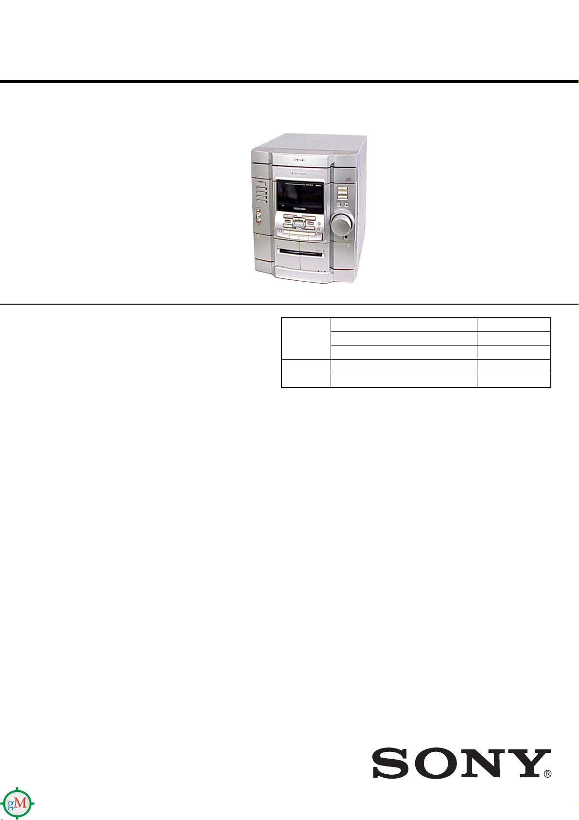
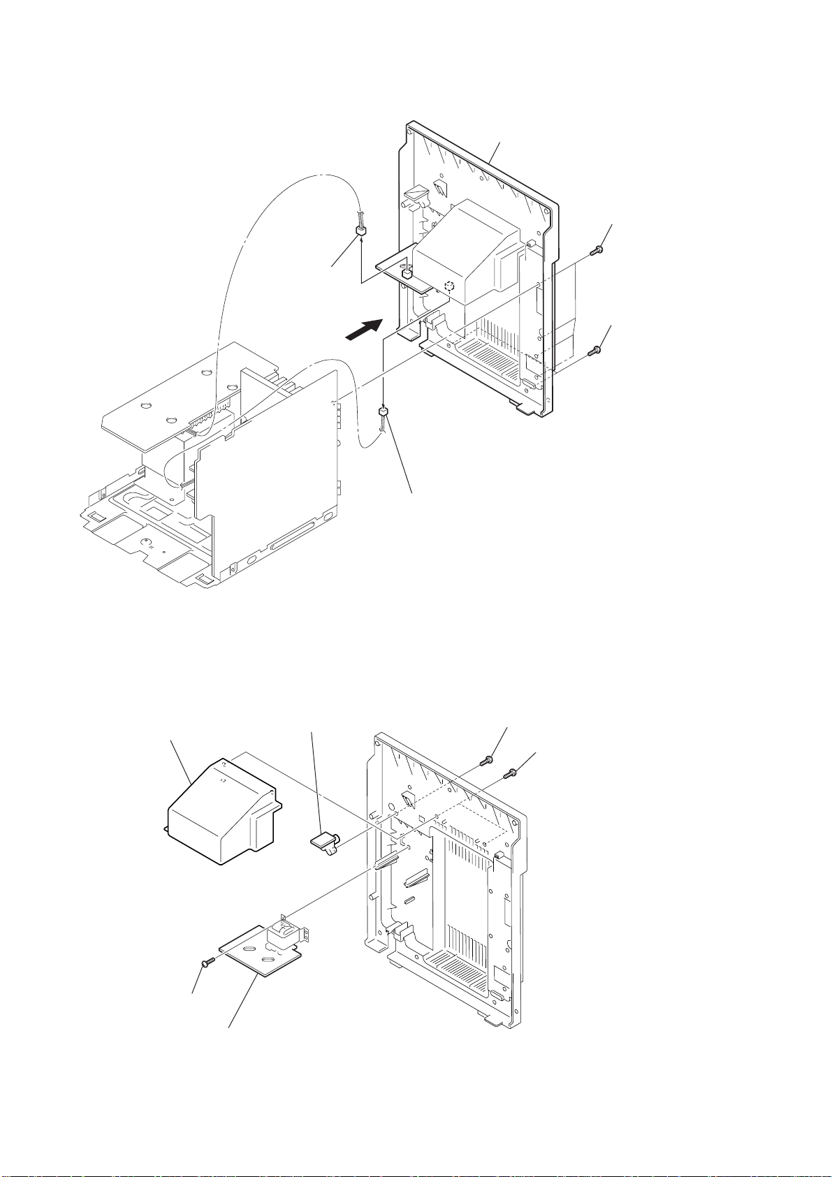
2-2. CD Door
)
CD mechanism deck (CDM58F-K6)
1
Turn the pulley to the direction of arrow.
Front panel side
4
CD door
HCD-RG110
pulley
2-3. Front Panel Section
6
connector 2p (CN682)
2
Pull-out the disc tray.
4
screw (+BVTP 3
×
3
10)
3
screw (+BVTP 3
qs
front panel
×
10)
7
wire (flat type)
19p (CN733)
5
0
connector 3p (CN303)
2
screw (+BVTP 3
8
9
wire (flat type) 13p (CN207)
×
connector 3p (CN201
10)
qa
connector 7p (CN202)
1
three screws (+BVTT 3
×
6)
7
Page 3
HCD-RG110
)
)
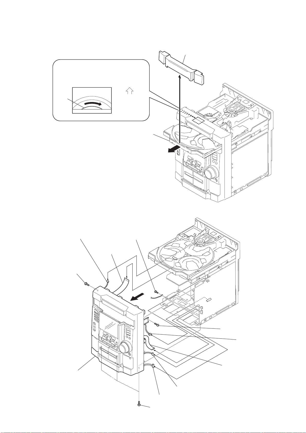
2-4. CD Mechanism Deck (CDM58F-K6)
4
CD mechanism deck (CDM58F-K6)
3
1
screw (+BVTP 3
2
connector 7p (CN734)
×
10
2-5. Tape Mechanism Deck (CWL43FF48)
3
tape mechanism deck
(CWL43FF48)
2
three ground wires
1
six
screws
(+BVTP 2.6
× 8
8
Page 4
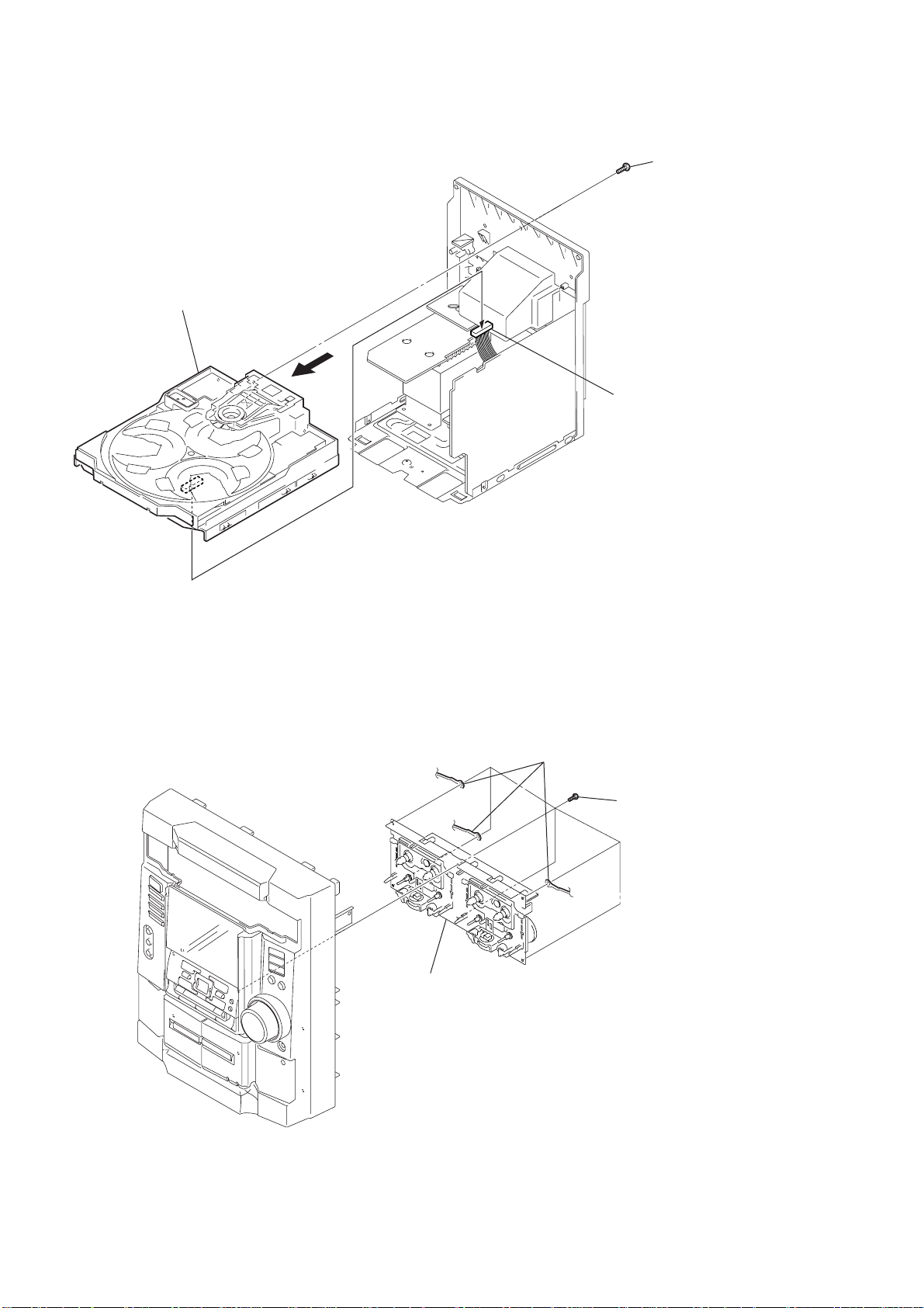
2-6. REM Board and PANEL Board
g
2
four
claws
two claws
6
REM
claw
board
REM
HCD-RG110
board
3
eight
(+BVTP 2.6
screws
× 8
)
1
volume knob
2-7. KEY Board
three claws
7
PANEL board
two claws
2
KEY board
5
Remove the solderin
(three portions)
4
connector
13p (CN662)
1 four
screws
(+BVTP 2.6
× 8
)
9
Page 5
HCD-RG110
)
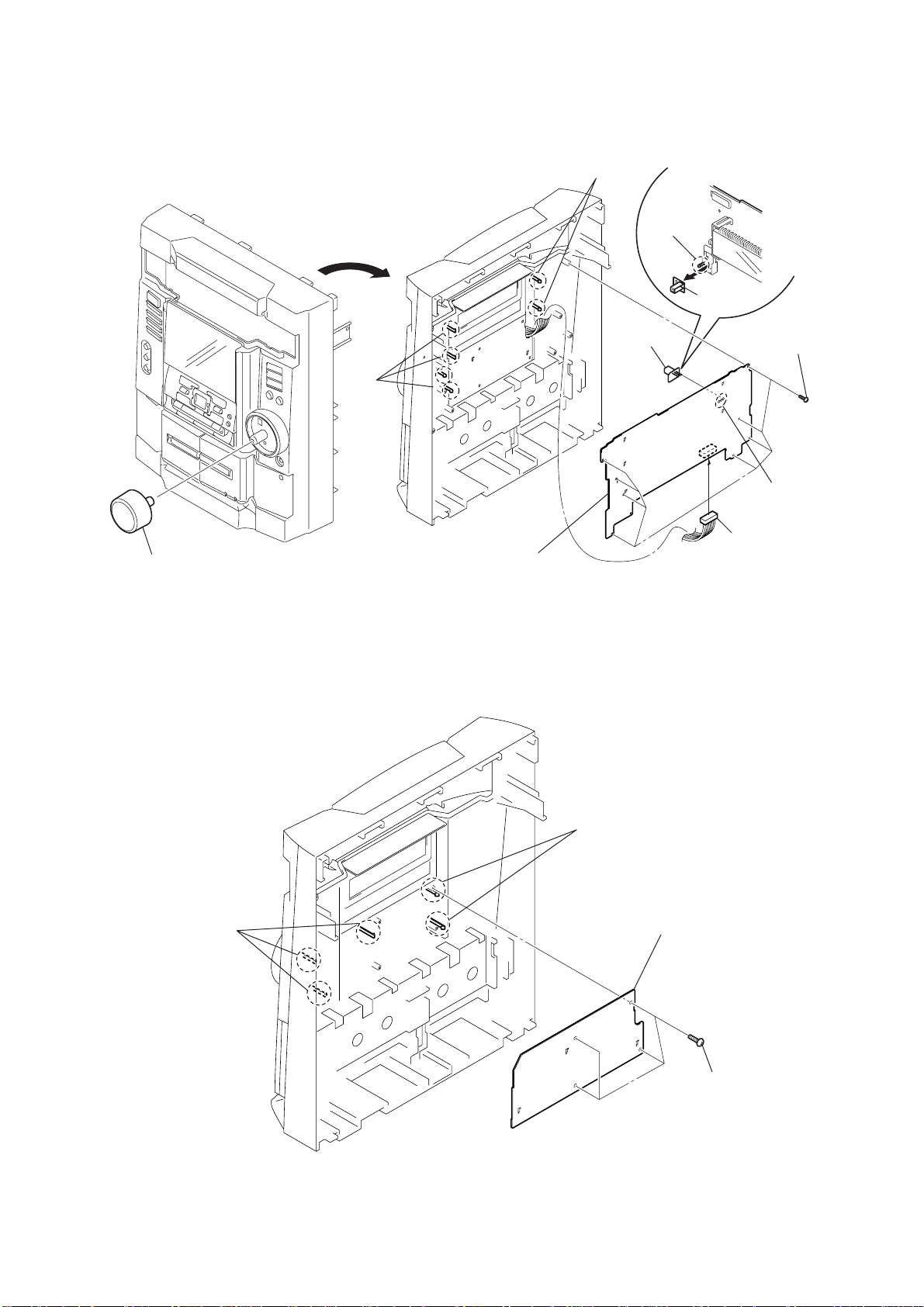
2-8. Back Panel Section
3
connector
3p (CN903)
5
6
back panel
1
four
screw
(+BVTP 3
2
two
screw
(+BVTT 3
×
×
10
6)
4
connector
2p (CN505)
2-9. SUB TRANS Board, VIDEO OUT Board and SENSOR Board
4
6
cover (duct)
VIDEO board
3
screw (+BVTP 3
5
two
×
10)
screws (+BVTP 3
×
10)
10
1
screw (+BVTP 3
×
10)
2
SUB TRANS board
Page 6
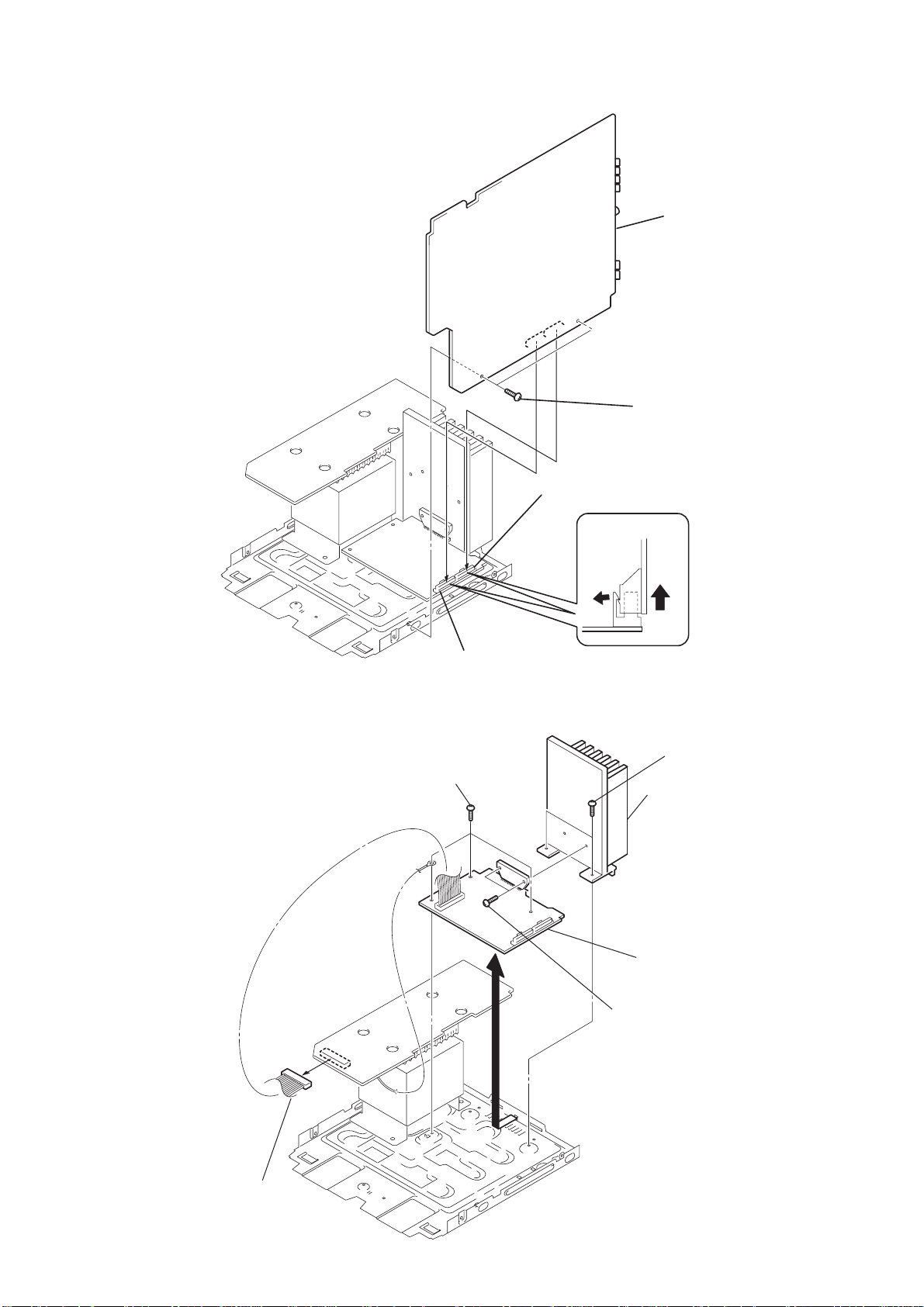
2-10. MAIN Board
)
4
MAIN board
1
screw (+BVTT 3
HCD-RG110
×
6
2-11. POWER Board
2 t
hree screws (+BVTT 3
2
connector 13p (CN503)
×
6)
3
connector 13p (CN502)
Main board
1 t
wo screws (+BVTT 3
7 h
eat sink
×
6)
5
connector 13p (CN915)
3
6 POWER
4 t
wo screws (+BVTP 3
board
× 1
6)
11
Page 7
HCD-RG110
)
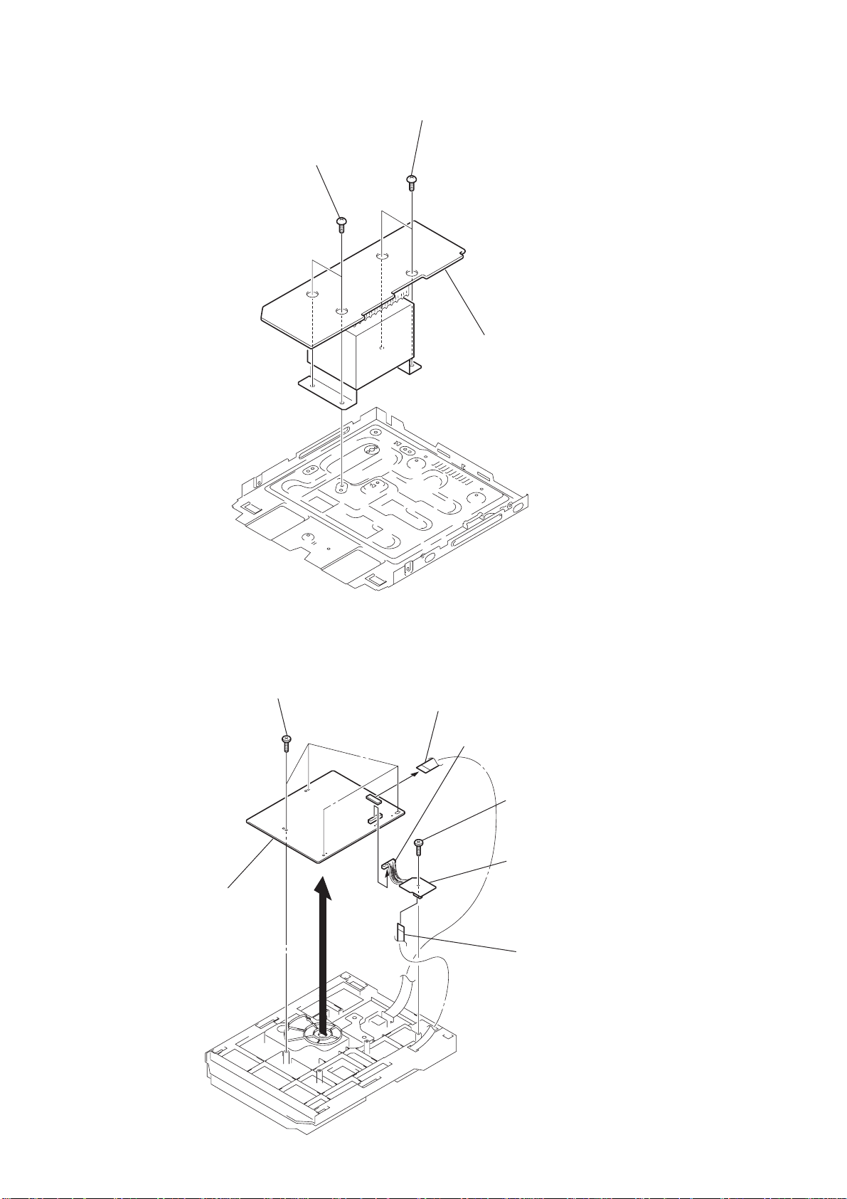
2-12. TRANS Board
screws (+BVTT 4 × 6)
1 two
2 two
screws (+BVTT 4 × 6)
3 TRANS board
2-13. CD Board and DRIVER Board
3
four s
crews (+BTTP M2.6 )
5
CD board
4
2
wire (flat type)
16p (CN731)
1
connector 10p (CN735)
6
Screw (+BTTP M2.6
8
DRIVER board
7
wire (flat type)
8p (CN702)
12
Page 8

2-14. SPDL Board
)
HCD-RG110
1 Remove solder (four places)
2 Remove solder (four places)
3 SPDL board
2-15. Optical Pick-up (KSM-213DCP)
7
two insulators
4
two stoppers (BU)
2
holder (BU) assy
0
optical pick-up
(KSM-213DCP)
9
1
screw (+PTPWH M2.6)
6
screw (DIA. 12)
8
two insulators
5 two
screws (+PTPWH M2.6
3
two screws (+BTTP M2.6)
13
Page 9

HCD-RG110
2-16. MOTOR Board, ADDRESS SENSOR Board
2
screw (+PTPWH 2.6
7
8
3
tray
screw (+BTTP M2.6)
×
8)
5
MOTOR board
two screws (+BTTP M2.6)
6
Remove the two solderings of motor.
4
connector 4p (CN722)
9
ADDRESS SENSOR board
1
Pull out the disc tray.
2-17. Table (New), Cam (Control) and DC Motor
*Cautions of an assembly
DC
motor (TURN)
pulley (S)
4 gear (U)
2 screw (STEP)
3 cam (CONTROL)
5 pulley (S)
6 belt
7 DC
claw
motor (TURN)
14
claw
1 table (NEW)
Page 10

http://getMANUAL.com
SECTION 3
TEST MODE
HCD-RG110
[Change-over of AM Tuner Step between 9 kHz and
10 kHz]
•A step of AM channels can be changed o ver between 9 kHz and
10 kHz. (Except AEP/UK models)
Procedure:
1. Press ?/1 button to turn the set ON.
2. Select the function “TUNER”, and press TUNER/BAND
button to select the BAND “AM”.
3. Press ?/1 button to turn the set OFF.
4. Press TUNER/BAND and ?/1 buttons simultaneously, and
the display of fluorescent indicator tube changes to “AM 9 k
STEP” or “ AM 10 k STEP”, and thus the channel step is changed
over.
[Cold Reset]
• The cold reset clears all data including preset data stored in the
RAM to initial conditions. Execute this mode when returning
the set to the customer.
Procedure:
1. Press three buttons x , GROOVE , and ?/1 simultaneously.
2. The fluorescent indicator tube displays “COLD RESET” and
the set is reset.
[Aging Mode]
This mode can be used for operation check of CD section and tape
deck section.
• If an error occurred:
The aging operation stops and is displayed status.
• If no error occurs:
The aging operation continues repeatedly.
1. Operating method of Aging Mode
Turn on the main power and select “CD” of the function.
1) Set three discs in tray. Select ALL DISCS, and REPEAT OFF.
2) Load the tapes recording use into both decks.
3) Press three buttons x , GAME EQ , and
DISC SKIP/EX-CHANGE simultaneously.
4) Aging operations of CD and tape are started at the same time.
5) To exit the aging mode, perform [Cold Reset].
2. Aging mode in CD section
1) Operation during aging mode
• In the agining mode ,the program is excuted in the following
sequence.
(1) The disc tray opens and closes.
(2) The disc tray turns to select a disc 3.
(3) The pickup accesses to the first track, and plays 3 seconds.
(4) The pickup accesses to the last track, and plays 3 seconds.
(5) The disc tray opens and closes.
(6) The disc tray turns to select a disc 1.
(7) The same operation starts like step (3).
(8) After a disc 1 aging operation, a disc 2 is selected.
(9) When an aging operation of a disc 3 is completed, the display
“AGING
∗∗∗∗” value increases.
(10) If no error occurs, the aging operation continues repeatedly.
2) Error display
Disc error
Display Error
E00D01022 Focus error (No disc)
E00D02022 Sub Q error (Focus is good)
E00D02023 TOC reading error
E00D02014 Access error (Unable within regular time)
Mechanism error
Display Error
E00M__E_0 Error during opening tray
E00M__C_2 EX-CHANGE disc error
E00M__D_0 Error during closing tray
E00M__F_3 EX-OPEN error
E00M__D_5 EX-CLOSE error
E00M__C_2 Chuck-up error
E00M__C_3 Unchucking error
3. Aging mode in Tape Deck section
1) Operation during aging mode
• In the agining mode, the program is excuted in the following
sequence.
Step
1
Rewind the TAPE A
2
Rewind the TAPE B
3
Play the TAPE A (1 minute)
4
Stop the TAPE A (1 second)
5
Play the TAPE A (3 minutes)
6
Rewind(AMS) the TAPE A
7
F.F.(AMS) the TAPE A
8
Play the TAPE B (1 minute)
9
Stop the TAPE B (1 second)
10
Record the TAPE B (3 minutes)
11
Rewind(AMS) the TAPE B
12
F.F.(AMS) the TAPE B
Operation
Display
TAPE AAG-1
TAPE BAG-2
TAPE AAG-2
TAPE AAG-3
TAPE AAG-4
TAPE AAG-5
TAPE AAG-6
TAPE BAG-2
TAPE BAG-3
TAPE BAG-4
TAPE BAG-5
TAPE BAG-6
2) Error display
• If error occurred, the display remains like “TAPE BAG-2”.
4. Exiting from the aging mode
• Be sure to perform Cold Reset to exit from the aging mode.
15
Page 11

HCD-RG110
[GC T est Mode]
• All fluorecent segments and LEDs are tested.
•Keyboard check.
Procedure:
1. Press ?/1 button to turn the set ON.
2. To enter the test mode, press the three buttons x , GAME EQ
and DISC 2 simultaneously.
3. All segments and LEDs (without STANDBY LED) are turned
on.
4. Press GAME EQ and DISC 2 buttons simultaneously, and the
key check mode is activated.
5. The message “KEY 0 0 0 0” is displayed.
Each time a button is pressed, the key code number is displayed.
6. Press GAME EQ and DISC 2 buttons simultaneously, and the
key count mode is activated.
7. The message “KEYCNT 0 1” is displayed.
Each time a button is pressed, “KEYCNT 0 1” value increased.
However, once a button is pressed, it is no longer taken into
account.
8. Press GAME EQ and DISC 2 buttons simultaneously, and the
head phone detect mode is activated.
9. The message “H_P OFF” is displayed when a headphone jack
is not inserted.
“H_P ON ” is displayed when a headphone jack is inserted.
10. Press GAME EQ and DISC 2 buttons simultaneously, and the
volume control detect mode is activated.
11. The message “VOLUME FLAT” is displayed.
“VOLUME UP” is displayed if rotating VOLUME knob
clockwise, or “VOLUME DOWN” is displayed if rotating
counterclockwise.
12. To exit from the GC test mode after the volume control detect
mode, press GAME EQ and DISC 2 buttons simultaneously .
[MC T est Mode]
•This mode is used to test the function of the equalizer.
Procedure:
1. Press ?/1 button to turn the set ON.
2. T o enter the test mode, press the three b uttons x , GAME EQ
and DISC 3 simultaneously.
3. Press the MOVIE EQ button.
The function of the equalizer is set to “MIN”.
4. Press the MUSIC EQ button.
The function of the equalizer is set to “MAX”.
5. Press the P.FILE button.
The function of the equalizer is set to “FLAT”.
6. To exit from this mode, press ?/1 button to turn the set OFF.
[CD Ship Mode (No Memory Clear) ]
•This mode moves the pickup to the position durable to vibra-
tion. Use this mode when returning the set to the customer after
repair.
Procedure:
1. Press ?/1 button to turn the set ON.
2. Select the function “CD”.
3. Press ?/1 button to turn the set OFF.
4. Press CD button and ?/1 button simultaneously.
5. The "STANDBY" display blinks instantaneously, and the CD
ship mode is set.
[Version and Destination Display Mode]
•The version or destination is displayed.
Procedure:
1. Press ?/1 button to turn the set ON.
2. To enter the test mode, press the three buttons x , GAME EQ
and MOVIE EQ simultaneously.
3. The destination is displayed.
4. Press STOP and GROOVE buttons simultaneously.
5. The version is displayed.
6. To exit from this mode, press ?/1 button to turn the set OFF.
[CD Service Mode]
•This mode can run the CD sled motor freely. Use this mode, for
instance, when cleaning the pickup.
Procedure:
1. Press ?/1 button to turn the set ON.
2. Select the function “CD”.
3. To enter the test mode, press three buttons x , GAME EQ ,
and OPEN/CLOSE simultaneously.
4. The CD service mode is selected.
5. With the CD in stop status, press
to outside track, or press . button to inside track.
6. To exit from this mode, perform as follows:
> button to mov e the pickup
+
–
1) Move the pickup to the most inside track.
2) Press ?/1 button to turn the set OFF.
Note: • Always move the pickup to most inside track when exiting from
this mode. Otherwise, a disc will not be unloaded.
• Do not run the sled motor excessively, otherwise the gear can be
chipped.
16
Page 12

SECTION 4
l
T101: NULL
IFT101: AM IF
RV101:
FM TUNED LEVEL
ELECTRICAL ADJUSTMENTS
HCD-RG110
TUNER SECTION
AM IF Adjustment
AM RF Signal generator
set
30% amplitude
modulation by
400Hz signal
output level : as low as possible
16
set
headphones jack (JK691)
Procedure:
1. Set the frequency of the AM RF signal generator to 1000 kHz
(at 10 kHz step) or 999 kHz (at 9 kHz step).
2. Tune the set to AM 1000 kHz (at 10 kHz step) or 999 kHz (at 9
kHz step).
3. Adjust IFT101 so that the reading on level meter becomes in
maximum.
AM ANTENNA termina
(JK103)
level meter
Ω
FM T uned Level Adjustment
FM RF Signal generator
75
Ω
coaxial
set
Carrier frequency : 98 MHz
Modulation : AUDIO 1 kHz, 75 kHz
deviation (100%)
Output level : 30 dB (at 75
Ω
open)
FM ANTENNA terminal
(JK103)
Procedure:
1. Supply a 98 MHz signal at 28 dB from the ANTENN A terminal.
2. Tune the set to 98 MHz.
3. Adjust RV101 to the point (moment) when the TUNED
indicator will change from going off to going on.
Adjustment Location: MAIN board
Null Adjustment
FM RF Signal generator
75
Ω
coaxial
set
Carrier frequency : 98 MHz
Modulation : AUDIO 1 kHz, 75 kHz
deviation (100%)
Output level : 60 dB (at 75
Ω
open)
FM ANTENNA terminal
(JK103)
Procedure:
1. Supply a 98 MHz signal at 60 dB from the ANTENN A terminal.
2. Tune the set to 98 MHz.
3. Measure voltage between pin 21 and pin 23 of IC 101. Adjust
T101 until the voltage becomes 0 V.
Adjustment Location: MAIN board
[MAIN BOARD] Component side
17
Page 13

HCD-RG110
p
CD SECTION
Note :
1. CD Block is basically designed to operate without adjustment.
Therefore, check each item in order given.
2. Use YEDS-18 disc (3-702-101-01) unless otherwise indicated.
3. Use an oscilloscope with more than 10MΩ impedance.
4. Clean the object lens by an applicator with neutral detergent
when the signal level is low than specified value with the
following checks.
RF Level Check
oscilloscope
CD board
IC751 pin q;
GND
Procedure :
1. Connect oscilloscope to pin q; (IC751).
2. Turned Power switch on.
3. Load a disc (YEDS-18) and playback.
4. Confirm that oscilloscope waveform is clear and check RF signal
level is correct or not.
Note : Clear RF signal waveform means that the shape “ ◊ ” can be clearly
distinguished at the center of the waveform.
RF signal waveform
VOLT/DIV : 200mV
TIME/DIV : 500ns
level : 1.4 to 2.1 Vp-
Adjustment Location: CD board
[CD BOARD] (Component Side)
CN731
CN733
18
IC751
IC731
TP731:
TP connected to pin q; (IC751)
Page 14

SECTION 5
5 Q209 Collector
(TAPE REC mode)
2 IC601 qd (XT2)
1 IC751 rf (XOUT)
4 IC102 ws (XOUT)
2 V/DIV, 100 ns/DIV
5 V/DIV, 10 s/DIV
2 V/DIV, 10 s/DIV
2 V/DIV, 20 ns/DIV
3 IC601 qh (CF2)
2 V/DIV, 40 ns/DIV
6 IC103 qf (XO)
1 V/DIV, 100 ns/DIV
5.2 Vp-p
5.6 Vp-p
59 ns
222 ns
30.5 s
4.9 Vp-p
100 ns
5.0 Vp-p
13.5 Vp-p
17 s
231 ns
DIAGRAMS
THIS NOTE IS COMMON FOR PRINTED WIRING BOARDS AND SCHEMATIC DIAGRAMS.
(In addition to this, the necessary note is printed in each block.)
HCD-RG110
5-1. Circuit Boards Location
Note on Schematic Diagram:
• All capacitors are in µF unless otherwise noted. pF: µµF
50 WV or less are not indicated except for electrolytics
and tantalums.
• All resistors are in Ω and 1/
specified.
f
•
• C : panel designation.
Note: The components identified by mark 0 or dotted line
• A : B+ Line.
• B : B– Line.
• H : adjustment for repair.
•Voltages and waveforms are dc with respect to ground
•Voltages are taken with a VOM (Input impedance 10 MΩ).
•Waveforms are taken with a oscilloscope.
• Circled numbers refer to waveforms.
• Signal path.
: internal component.
with mark 0 are critical for safety.
Replace only with part number specified.
under no-signal (detuned) conditions.
Voltage variations may be noted due to normal produc-
tion tolerances.
no mark : FM
< >: CD
[]: TAPE
Voltage variations may be noted due to normal production tolerances.
F : FM
E : PB (DECK A)
d : PB (DECK B)
G : REC (DECK B)
J : CD
4
W or less unless otherwise
Note on Printed Wiring Boards:
• X : parts extracted from the component side.
• b : Pattern from the side which enables seeing.
• Indication of transistor.
C
These are omitted.
Q
B
CE
These are omitted.
Q
B
E
SUB TRANS board
PANEL board
KEYBOARD board
DRIVER board
ADDRESS SENSOR board
REM board
CD board
MAIN board
MOTOR board
VIDEO OUT board
SPDL board
TRANS board
POWER board
• Waveforms
19 19
Page 15

HCD-RG110
5-5. Schematic Diagram – CD Section –
CD BOARD
OPTICAL PICK-UP
BLOCK
(KSM-213DCP)
CN731
• See page 34,35 for IC Block Diagrams. • See page 19 for Waveforms.
LD DRIVER
4.9
4.2
1.6
50V
IC731
FOCUS/TRACKING/SLED/
SPINDLE SERVO,RF AMP
IC731
LA9242M
IC B/D
IC751
DIGITAL SIGNAL
PROCESSOR
IC751
LC78622NE
IC B/D
CN733
TO
PANEL BOARD
A
CN602
(Page 31)
SWITCH
0
0.8
0.8
1
/
10
10
10
0.6
0.2
MUTE
0.6
MUTE
0.0015
TO
MAIN BOARD (1/4)
B
CN704
(Page 26)
0
0.0015
CN734
SPDL
BOARD
M01
( )
M02
( )
( )
CN01
CN732
MM1469XH
IC B/D
IC781
IC781
FCS/TRK COIL,
SL/SP MOTOR
DRIVER
4.7k
CN735
DRIVER BOARD
CN701
IC701
MOTOR
DRIVER
IC B/D
0
4.1
0.1
0.1
ADDRESS SENSOR BOARD
0
0.7
SWITCH
1.2
(UP/DOWN)
SG-264
0.1
(OPEN/CLOSE)
CN722CN711
(TURN)
MTZJ-3.9A
CN702CN721
0
7.7
7.7
IC711
TABLE SENSOR
MOTOR BOARD
No mark:CD
2424
Page 16

HCD-RG110
5-7. Schematic Diagram – MAIN Board (1/4) –
ANTENNA
• See page 34 for IC Block Diagrams. • See page 19 for Waveforms.
MAIN BOARD (1/4)
+B SWITCH
R122
680
J137
C133 33p
J134
33pC148
RF IF
AMP
5.6
11.8
9.6
4.9
11.9
0
RV101
FM TUNED
LEVEL
0.022
0.022
IC101
AM FM IF MPX
100
330k
560p
BUFF
4
5
0.01
3.5
1.3
0.6
2.4
6
2.3
0.1
0.01
0.01
4.7
2.5
2.5
0
2.5
IC B/D
IC103
RDS
4.7
2.3
1.7
0.01
6
3
TO
MAIN BOARD
(3/4)
B
TO
CD
BOARD
CN734
(Page 24)
CN704
IC102
PLL
IC B/D
2.1
2.2
3.4
88
3.1
3.1
0.3
6.42.3
2.3
4
2.3
1
2.6
2.6
1
000
0
2.6
5.3
0
5.1
6.9
0
0
0
0
LA1845N
2.3
IFT101
AM IF
2.3
2.5
8
4.5
8.1
T101
NULL
3.4
IC B/D
0
6.9
3.4
9
4
10
7
0
MUTE
0.2
0
15k
15k
0.2
MUTE
8
2
11
12
13
14
15
16
TO
MAIN BOARD
(3/4)
TO
MAIN BOARD
(2/4)
4
TO
MAIN BOARD
17
(3/4)
18
1
TO
MAIN BOARD
1
(2/4)
2 3
2626
Page 17

HCD-RG110
5-8. Schematic Diagram – MAIN Board (2/4) –
TAPE
DECK
(1/2)
DECK A
DECK B
MAIN BOARD
(2/4)
0.6
2.9
0.6
0
0
0
4.5
0
0.6
0.6
2.9
2.9
IC201
DECK A/B SELECT
PB/REC EQ AMP
• See page 19 for Waveforms.
4.7
4.8
4.7
2.4
4.8
2.5
3.7
0.2
9.4
HA12237F
1.2
2.9
4.7
4.7
4.8
50V
4.7
1.2
3.3k
TO
MAIN BOARD
(3/4)
3.3k
TO
MAIN BOARD
(1/4)
1 6
2019 121 222 24
MAIN BOARD
3
TO
(3/4)
IC303
BUFFER
5.9
0.2
11.5
SPEANA(R)
AMS
5.9
7.1
1.2
0.6
0.1 50v
5.6
AMS
0.8
0.2
8.2k
5.9
5.7
1.3
R265
150k
5.1
3.4
AMS
2.7
0.8
0.7
SPEANA(L)
5.5
23
TO
MAIN BOARD
(1/4)
TO
MAIN BOARD
2
27
(3/4)
85
25 28 291287 11 26
30
7
TO
MAIN BOARD
(4/4)
31
5
22k
SWITCH
0
12
470
11.9
11.9
0
50V
BIAS
11.9
0.7
11.2
SWITCH
0
12
0
REC BIAS
0
0.7
0
0.7
0
Q201-204
SWITCH
0.7
0.7
BIAS OSC
0
0
0
Q222,223
B SOL DRIVE
0
9.1
0
9.1
0
9.1
A SOL DRIVE
9.1
9.1
Q224,225
9
0
9.1
9
0
220p
9
0
Q226,227
M +B CONT
TAPE DECK
(2/2)
4.8
3.4
4.7
IC202
BUS SHIFT
REGISTER
0
0
0
0
4.7
4.8
4.804.7
4.8
0
5
4
4.7
0.2
4.4
RESET
0.2
4.4
4.7
0
BU1924 CLK
BU1924 DATA
CN603
TO
PANEL BOARD
C
CN601
(Page 31)
32
33
34
35
36
37
38
39
40
41
42
43
44
45
46
47
48
27 27
Page 18

HCD-RG110
5-9. Schematic Diagram – MAIN Board (3/4) –
MAIN BOARD
4
5
3
6
TO
MAIN BOARD
(1/4)
23
24
6
22
TO
MAIN BOARD
(2/4)
• See page 34 for IC Block Diagrams.
(3/4)
BUFFER
11.4
4.4
4.7
BUFFER
11.4
4.3
4.6
IC804
+5V REG
5
12
24.6
13.6
13.6
13.6
13.6
SWITCH
13.6
IC803
+5.6V REG
13.65.6
4.8
0.6
GND1
CN402
F
9
15.4
TO
POWER BOARD
CN502
(Page 33)
4
TO
MAIN BOARD
(1/4)
IC801
IC301
SOUND PROCESSOR
4.6
4.6
4.6
4.6
9
10
13
14
15
16
17
18
4.6
4.6
4.6
4.6
4.6
4.6
4.6
220p
IC B/D
0.7
4.6
4.6
4.6
4.6
4.6
4.6
4.6
4.6
9.2
0
0
220p
0.22
0.22
0.22
0.22
IC802
+12V REG
+9V REG
11.9
0
PROTECT CONT
4.3
0
RELAY DRIVE
12
2.9
0
Q806,813
PROTECT SWITCH
0.7
RELAY DRIVE
0
0
0.8
0
TO
MAIN
BOARD
(2/4)
2627
TO
MAIN
8 95
BOARD
(2/4)
5020 1921 512829 52 53 5425 55
49
58596061626364656667 69 70 80 71 74 75 76 77 78 79
TO
MAIN
BOARD
(4/4)
2828
Page 19

5-10. Schematic Diagram – MAIN Board (4/4) –
49 50 51 52 53 54 55 58596061626364656671 67 69 70 80 74 75 76 77 78 79
http://getMANUAL.com
TO
MAIN BOARD
9
(3/4)
HCD-RG110
MAIN BOARD
(4/4)
Q313,314
MUTE CONT
30
BUFFER
5.8
1.5
6.6
1.2
2.1
BUFFER
1.9
BUFFER
000 00
BUFFER
4.4 4.4 4.4 4.4
0.7
4.0
BUFFER
12
11.8
0
0
27k
BUFFER
0.7
4.7k
Q315,316
MUTE
0.7
0.7
56k
BUFFER
0
+
JK303
+
SPEAKER
0
BUFFER
27k
Q809,810
PROTECT DETECT
11.9
11.9
0
0
0
0
L351
10
R396
Q331,332
MUTE
L352
R397
10
-
-
7
TO
MAIN BOARD
(2/4)
E
0
0.7
0.7
0
SWITCH
31
32
33
34
35
36
37
38
39
40
41
42
43
44
45
46
47
48
4.4 4.4
SWITCH
4.4 4.4
4
SWITCH
4
5.6
SWIITCH
11.1
4.8
0
CN403
TO
PANEL
BOARD
CN691
(Page 31)
D
TO
POWER
BOARD
CN503
(Page 33)
29 29
Page 20

HCD-RG110
5-12. Schematic Diagram – PANEL Section –
KEY BOARD BOARD
GAME MIXING
4.9
0
BUFFER
11ES2-TB5
10K
• See page 36 for IC Pin Function Description. • See page 19 for Waveforms.
+
REM BOARD
RM601
REMOTE CONTROL
RECEIVER
NJL64H00A-1
5.1
5.1
OPEN/CLOSE
/START
EX-CHANGE
VOLUME
SEL2410G
GAME MIXING
E
TO
MAIN BOARD(4/4)
CN303
(Page 29)
JK691
PHONES
VIDEO OUT
BOARD
JK602
VIDEO
OUT
IC602
RESET
4.8
5.1
-23.8
0
5.155.1
5.1
5.1
5.1
0.3
-23.8
-23.8
-23.8
-23.8
-23.8
-23.8
-23.6
-23.6
-23.6
-23.6
-23.6
-14.9
-12.4
-12.5
-25
4.9
-20
-17.5
-22.5
-25.1
-25.4
-15
-22.5
-25.2
-22.5
-17.5
-15
-17.5
-17.5
0.4
-15
10K
0.9
5.1
5.1
4.9
2.7
2.4
3 2
IC601
SYSTEM CONTROL
IC601
LC876662W-5Z80
-25.2
-25.3
-1.5
-20.2
-17.5
-25.2
D606 1SS133
32.768kHz
4.7M
2.5
2.2
4.950
4.9
4.90004.9
0
0
4.9
0
0
000
4.9
0.2
4.9
4.9
0
100
0
0
0
5.1
0
0
0
5
5
5
5
0.3<4.9>
4.9<0.4>
5
4.3
0.2
5
5
4.6
4.8
4.8
4.8
SEL2110R
SEL2810D-C
SEL2810D-C
A/B
SEL2810D-C
/BAND
SEL2810D-C
VIDEO
GAME
INPUT
27k
AUDIO
JK681
27k
CN601
TO
MAIN BOARD
(2/4)
C
CN603
(Page 27)
CN602
TO
CD BOARD
CN733
A
(Page 24)
PANEL BOARD
J
FLD601
No mark:FM
< >:CD(stop)
31 31
Page 21

5-14. Schematic Diagram – POWER/TRANS Section –
HCD-RG110
POWER BOARD
IC501
POWER AMP
(1/2)
STK402-070S
-0.2
-0.2
-0.2
C512
0.001
(1/2)
TRANS BOARD
F914
C509
22
50V
36.5
0
-36
-34.7
0
MUTE
37.7
0
-37.7
37.7
37.7 11.6
C559
22
Q503,504
37.1
MUTE CONT
0
0.6
R510 0.22/2W
R508 0.22/2W
0
11.6
0
LOAD DETECT
OVER
0
OVER
LOAD DETECT
0
D541
D5SBA20-4101
C542
2200
50V
C592
2200
50V
SUB TRANS BOARD
RELAY DRIVE
0.7
T6.3AL/250V
F920 T6.3AL/250V
0.1
5.7
-25.6
9
POWER TRANSFORMER
-30V GREG
-36
-26.1
(MAIN)
220V
POWER
TRASFORMER
(SUB)
C901 0.01 250V
-0.2
IC501
POWER AMP
STK402-070S
(2/2)
(2/2)
0
0
R558 0.22/2W
R560 0.22/2W
MAIN BOARD (4/4)
D
TO
CN403
(Page 29)
FAN ON
MAIN BOARD (3/4)
F
TO
CN402
(Page 28)
No mark:FM
IC901
+5.6V REG
33 33
 Loading...