

Page 1
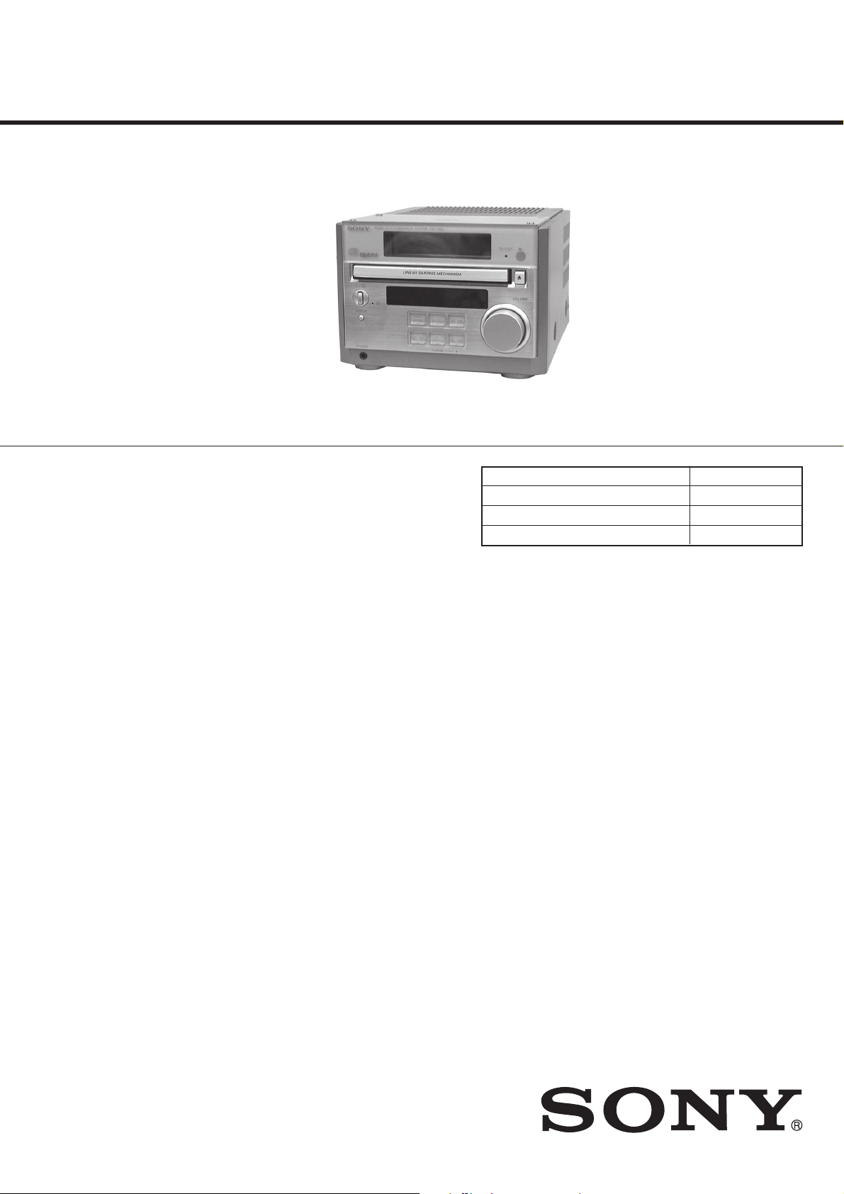
HCD-RB5
SERVICE MANUAL
Ver 1.1 2001. 12
• This set is the Amplifier and CD player
section in CMT-RB5.
SPECIFICATIONS
Main Unit
Amplifier section
For the U.S. model
AUDIO POWER SPECIFICATIONS
POWER OUTPUT AND TOTAL HARMONIC
DISTORTION:
With 4-ohm loads, both channels driven, from
120 – 10,000 Hz; rated 15 watts per channel
minimum RMS power, with no more than 10%
total harmonic distortion from 250 milliwatts to
rated output.
US, Canadian and Mexican models:
Continuous RMS power output (reference):
European and Australian models:
DIN power output (Rated):12 + 12 watts
Continuous RMS power output (Reference):
Music power output (Reference):
Other models:
The following measured at 220 V AC, 50/60 Hz
DIN power output (rated): 10 + 10 watts
Continuous RMS power output (reference):
The following measured at 240 V AC, 50/60 Hz
DIN power output (rated): 12 + 12 watts
Continuous RMS power output (reference):
15 + 15 watts
(4 ohms at 1 kHz, 10% THD)
(4 ohms at 1 kHz, DIN)
15 + 15 watts
(4 ohms at 1 kHz,
10% THD)
28 + 28 watts
(4 ohms at 1 kHz, DIN)
12 + 12 watts
(4 ohms at 1 kHz, 10% THD)
(4 ohms at 1 kHz, DIN)
15 + 15 watts
(4 ohms at 1 kHz, 10% THD)
Inputs
MD/VIDEO (AUDIO) IN (phono jacks):
Outputs
MD/VIDEO (AUDIO) OUT (phono jack):
PHONES (stereo minijack):
SPEAKER: accepts impedance of 4 to
CD DIGITAL OUT OPTICAL:
CD player section
System Compact disc and digital audio
Laser Semiconductor laser (λ=780 nm)
Laser output MAX. 44.6 µW*
Frequency response 2 Hz – 20 kHz
Tuner section
FM stereo, FM/AM superheterodyne tuner
FM tuner section
Tuning range
US, Canadian model: 87.5 – 108.0 MHz
Other models: 87.5 – 108.0 MHz
Antenna FM lead antenna
Antenna terminals 75 ohms unbalanced
Intermediate frequency 10.7 MHz
voltage 500/250 mV, impedance
47 kilohms
voltage 250 mV, impedance
1 kilohm
accepts headphones of 8 ohms or
more.
16 ohms.
Optical
system
Emission duration: continuous
*This output is the value measured
at a distance of 200 mm from the
objective lens surface on the
Optical Pick-up Block with 7 mm
aperture.
(100 kHz step)
(50 kHz step)
US Model
Canadian Model
AEP Model
UK Model
E Model
Australian Model
Chinese Model
Model Name Using Similar Mechanism NEW
CD Mechanism Type CDM55C-K6BD38
Base Unit Name BU-K6BD38
Optical Pick-up Name KSM-213DCP
AM tuner section
Tuning range
US, Canadian model: 530 – 1,710 kHz
European model: 531 – 1,602 kHz
Other models: 531 – 1,602 kHz
Antenna AM loop antenna
Intermediate frequency 450 kHz
General
Power requirements
US, Canadian model: 120 V AC, 60 Hz
European model: 230 V AC, 50/60 Hz
Australian model: 220 – 240 V AC, 50/60 Hz
Korea, Chinese model: 220 V AC, 50/60 Hz
Mexican model: 120 V AC, 60 Hz
Other models: 110 – 120 V or 220 – 240 V AC,
Power consumption
US, Canadian and Mexican models:
Other models: 45 watts
Dimensions (w/h/d) Approx. 180 × 130 × 315 mm
Mass Approx. 4.0 kg
Supplied accessories Remote (1)
Design and specifications are subject to change
without notice.
(with the interval set at 10 kHz)
531 – 1,710 kHz
(with the interval set at 9 kHz)
(with the interval set at 9 kHz)
(with the interval set at 9 kHz)
530 – 1,710 kHz
(with the interval set at 10 kHz)
External antenna terminals
50/60 Hz
Adjustable with voltage selector
50 watts
incl. projecting parts and controls
Size AA (R6) batteries (2)
AM loop antenna (1)
FM lead antenna (1)
Speaker cords (2)
9-929-526-12
2001L1600-1
© 2001.12
MICRO Hi-Fi COMPONENT SYSTEM
Sony Corporation
Home Audio Company
Published by Sony Engineering Corporation
Page 2
Ver 1.1 2001.12
TABLE OF CONTENTS
1. GENERAL ·········································································· 4
2. DISASSEMBLY ································································ 6
3. SERVICE MODE ······························································ 9
4. ELECTRICAL ADJUSTMENTS ······························· 10
5. DIAGRAMS
5-1. Waveforms··································································· 11
5-2. Circuit Boards Location ·············································· 11
5-3. PRINTED WIRING BOARD –BD SECTION– ·······12
5-4. SCHEMATIC DIAGRAM –BD SECTION–············ 13
5-5. PRINTED WIRING BOARDS
–MAIN SECTION– ··················································· 14
5-6. SCHEMATIC DIAGRAM
–MAIN SECTION(1/2)– ··········································· 15
5-7. SCHEMATIC DIAGRAM
–MAIN SECTION(2/2)– ··········································· 16
5-8. PRINTED WIRING BOARDS
–POWER SECTION– ················································ 17
5-9. PRINTED WIRING BOARD
–PANEL SECTION– ················································· 18
5-10. SCHEMATIC DIAGRAM
–PANEL SECTION– ················································· 19
5-11. SCHEMATIC DIAGRAM
–LOADING SECTION–············································ 20
5-12. PRINTED WIRING BOARDS
–LOADING SECTION–············································ 20
5-13. IC Pin Function ·························································· 20
5-14. IC Block Diagrams····················································· 22
6. EXPLODED VIEWS ................................................... 23
7. ELECTRICAL PARTS LIST ................................... 28
NOTES ON HANDLING THE OPTICAL PICK-UP
BLOCK OR BASE UNIT
The laser diode in the optical pick-up block may suffer electrostatic
break-down because of the potential difference generated by the
charged electrostatic load, etc. on clothing and the human body.
During repair, pay attention to electrostatic break-down and also
use the procedure in the printed matter which is included in the
repair parts.
The flexible board is easily damaged and should be handled with
care.
NOTES ON LASER DIODE EMISSION CHECK
The laser beam on this model is concentrated so as to be focused on
the disc reflective surface by the objective lens in the optical pickup block. Therefore, when checking the laser diode emission,
observe from more than 30 cm away from the objective lens.
Notes on chip component replacement
• Never reuse a disconnected chip component.
• Notice that the minus side of a tantalum capacitor may be dam-
aged by heat.
Flexible Circuit Board Repairing
• Keep the temperature of the soldering iron around 270 ˚C during repairing.
• Do not touch the soldering iron on the same conductor of the
circuit board (within 3 times).
• Be careful not to apply force on the conductor when soldering
or unsoldering.
Unleaded solder
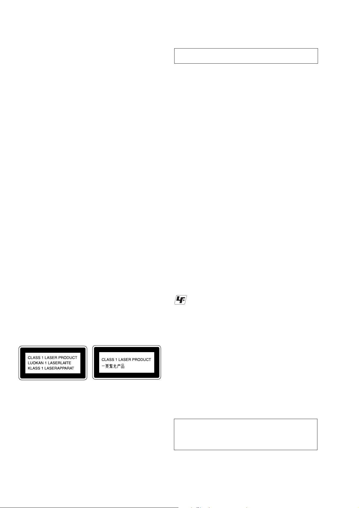
Boards requiring use of unleaded solder are printed with the leadfree mark (LF) indicating the solder contains no lead.
(Caution: Some printed circuit boards may not come printed with
the lead free mark due to their particular size.)
This appliance is classified as a CLASS 1 LASER product.
The CLASS 1 LASER PRODUCT MARKING is located on
the rear exterior.
Laser component in this product is capable of emitting radiation
exceeding the limit for Class 1.
: LEAD FREE MARK
Unleaded solder has the following characteristics.
• Unleaded solder melts at a temperature about 40°C higher than
ordinary solder.
Ordinary soldering irons can be used but the iron tip has to be
applied to the solder joint for a slightly longer time.
Soldering irons using a temperature regulator should be set to
about 350°C.
Caution: The printed pattern (copper foil) may peel away if the
heated tip is applied for too long, so be careful!
• Strong viscosity
Unleaded solder is more viscous (sticky , less prone to flow) than
ordinary solder so use caution not to let solder bridges occur
such as on IC pins, etc.
• Usable with ordinary solder
It is best to use only unleaded solder but unleaded solder may
also be added to ordinary solder.
CAUTION
Use of controls or adjustments or performance of procedures
other than those specified herein may result in hazardous
radiation exposure.
2
Page 3

SAFETY CHECK-OUT
After correcting the original service problem, perform the
following safety checks before releasing the set to the customer:
Check the antenna terminals, metal trim, “metallized” knobs, screws,
and all other exposed metal parts for A C leakage. Check leakage as
described below.
LEAKAGE
The A C leakag e from any exposed metal part to earth g round and
from all exposed metal parts to any exposed metal part having a
return to chassis, must not exceed 0.5 mA (500 microamperes).
Leakage current can be measured by any one of three methods.
1. A commercial leakage tester, such as the Simpson 229 or RCA
WT -540A. F ollow the manufactur ers’ instructions to use these
instruments.
2. A battery-operated AC milliammeter. The Data Precision 245
digital multimeter is suitable for this job.
MODEL IDENTIFICATION
– Back Panel –
Power Voltage
Indication
3. Measuring the voltage drop across a resistor by means of a
VOM or battery-operated A C voltmeter . The “limit” indication
is 0.75 V, so analog meters must have an accurate lo w-v olta ge
scale. The Simpson 250 and Sanwa SH-63Trd ar e examples of
a passive VOM that is suitable. Nearly all battery operated
digital multimeters that have a 2V AC range are suitable. (See
Fig. A)
To Exposed Metal
Parts on Set
AC
0.15 µF
Fig. A. Using an AC voltmeter to check AC leakage.
1.5 kΩ
Earth Ground
Voltmeter
(0.75 V)
Model
US, CND, MX models
AEP, UK, AED, EE models
AUS, CIS, CH, models
AC: 220 – 240V 50/60 Hz 45 W
E, AR, HK, MY,
SP, TW models
KR
• Abbreviation
CND : Canadian model. AUS : Australian model.
SP : Singapore model. MY : Malaysia model.
AR : Argentine model. AED : North European model.
MX : Mexican model. KR : Korean model.
EE : East European model. HK : Hong Kong model.
TW : Taiwan model. CH : Chinese model.
SAFETY-RELATED COMPONENT WARNING!!
COMPONENTS IDENTIFIED BY MARK 0 OR DOTTED LINE WITH
MARK 0 ON THE SCHEMATIC DIAGRAMS AND IN THE PARTS
LIST ARE CRITICAL TO SAFE OPERATION. REPLACE THESE
COMPONENTS WITH SONY PARTS WHOSE PART NUMBERS
APPEAR AS SHOWN IN THIS MANUAL OR IN SUPPLEMENTS
PUBLISHED BY SONY.
Power Voltage
Incdication
AC: 120 V 60 Hz 50 W
AC: 230 V 50 Hz 45 W
AC: 110 – 120/
220 – 240 V 50/60 Hz 45 W
AC: 220 V – 60 Hz 45 W
ATTENTION AU COMPOSANT AYANT RAPPORT
LES COMPOSANTS IDENTIFÉS PAR UNE MARQUE 0 SUR LES
DIAGRAMMES SCHÉMATIQUES ET LA LISTE DES PIÈCES SONT
CRITIQUES POUR LA SÉCURITÉ DE FONCTIONNEMENT. NE
REMPLACER CES COMPOSANTS QUE PAR DES PIÈSES SONY
DONT LES NUMÉROS SONT DONNÉS DANS CE MANUEL OU
DANS LES SUPPÉMENTS PUBLIÉS PAR SONY.
À LA SÉCURITÉ!
3
Page 4

LOCATION OF CONTROLS
– Front Panel –
1
SECTION 1
GENERAL
3q;495
6
2
qs
qa
1 ?/1 button
2 DISPLAY button
3 TUNER/BAND button
4 7 button
5 FUNCTION button
6 Z button
7 VOLUME knob
8 J L button
9 s button
q; l j button
qa PHONE jack
qs t indicator
7
8
4
Page 5
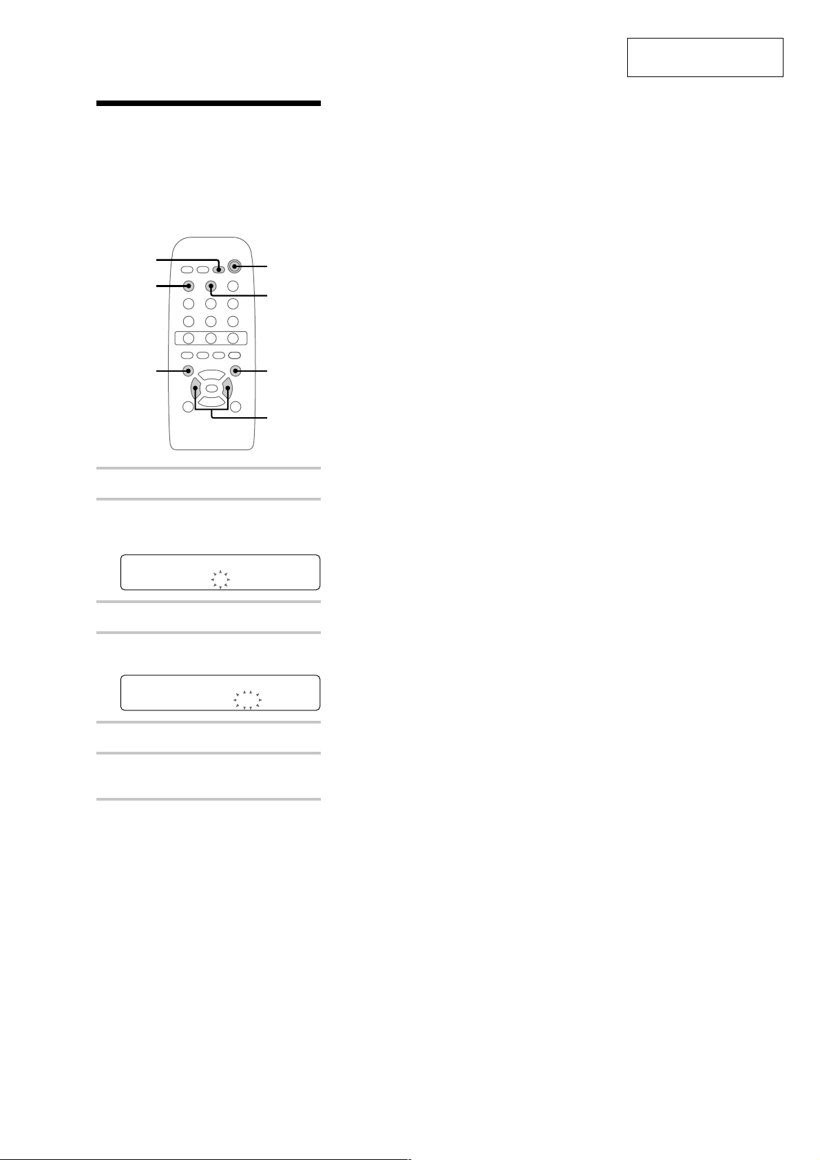
Step 2: Setting the time
You must set the time beforehand to use the timer
functions.
The clock is on a 24-hour system for the European
model, and a 12-hour system for other models.
The 24-hour system is used for illustration
purposes.
2
DISPLAY
?/1
1
4,6
NX x
This section is extracted
from instruction manual.
If you made a mistake
Press m/M repeatedly until the incorrect item
flashes, then set it again.
To change the preset time
You can change the preset time while the system
is off.
1 Press DISPLAY to display the clock.
2 Press CLOCK/TIMER SET.
3 Repeat steps 3 to 6 of “Setting the time.”
Tips
• The upper dot of the colon flashes for the first 30
seconds, and the lower dot flashes for the last 30
seconds of each minute.
• Each time you press DISPLAY while the system is
off, the display switches between no display and the
clock display.
m
1
Turn on the system.
2
Press CLOCK/TIMER SET.
The clock appears and the hour indication
flashes.
.
Mm
>
0:00
3
Press ./> to set the hour.
4
Press ENTER or M.
The minute indication flashes.
11:00
5
Press ./> to set the minute.
4
3,5
6
Press ENTER.
The clock starts.
5
Page 6

SECTION 2
)
DISASSEMBLY
Note: Follow the disassembly procedure in the numerical order given.
2-1. CASE (TOP)
6
two case screws
1
four screws
8
2
plate top
case (left)
7
one screw
(BVTP3
×
10)
qa
case (top)
q;
one screw
(BVTP3
×
10)
qs
back panel
9
eight screws
(BVTP3
4
one screw
(BVTP3
×
10)
×
10
2-2. FRONT PANEL ASSY
2
connector
(CN202)
3
one screw
(BVTP3
5
case (right)
3
two case screws
4
lug
×
8)
1
5
two screws
(BVTP3
×
8)
6
front panel assy
wire (flat type)(23 core)
(CN441)
6
Page 7
2-3. CD MECHANISM DECK (CDM55C-K6BD38)
4
CD mechanism deck
(CDM55C-K6BD38)
3
screw
(BVTP3 × 8)
1
wire (flat type)
(19 core)(CN401)
2
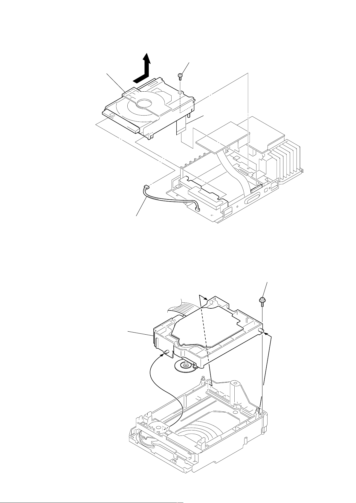
2-4. BASE UNIT (BU-K6BD38)
2
base unit
(BU-K6BD38)
connector
(CN1)
1
floating screw
(PTPWHM2.6)
7
Page 8

2-5. LOADING BOARD
)
3
Pull the tray pushing B.
B
2
belt (CDM55)
A
1
Rotate the gear(B) in
the direction of arrow
A
.
4
2-6. CAM (CDM55C-K6BD38)
1
torsion spring
2
lever (SW)
two screws
(BTP2.6
×
6)
6
gear (B)
3
spacer (55)
5
LOADING board
4
pulley (LDG)
5
gear (A)
7
roller
8
cam (CDM55
8
Page 9

SECTION 3
SERVICE MODE
[Panel Test Mode]
Procedure:
1. Set to standby state.
2. Press three buttons of s , ?/1 , and 7 simultaneously.
3. Liquid crystal display and LED are all turned on.
4. Pless Z to enter the version display mode.
5. Press 7 to enter the KEY, VOL, check mode. ( l j
and J L must be pressed for several seconds.)
6. To exit from this mode, press the buttons in the same way as
step 2.
[Aging Mode]
This mode can be used for operation check of CD section.
Procedure:
1. Load a CD disc.
2. Set to standby state.
3. Press three buttons of s , DISPLAY , and 7 simultaneously .
4. The aging is executed in bellow sequence.
5. To exit from the aging mode, press the ?/1 b utton to turn the
power OFF.
[Cold Reset]
Clears all the memories and starts up the machine again.
Procedure:
1. Set to standby state.
2. Press three buttons of s , ?/1 , and FUNCTION simultaneously.
[Hot Reset]
Starts up the machine again holding the memory data.
Procedure:
1. Set to standby state.
2. Press three buttons of s , ?/1 , and FUNCTION simultaneously.
9
Page 10

e
TP(TEO)
TP(VC)
BD board
Oscilloscope
)
SECTION 4
ELECTRICAL ADJUSTMENTS
CD SECTION
Note :
1. CD Block is basically designed to operate without adjustment.
Therefore, check each item in order given.
2. Use YEDS-18 disc (3-702-101-01) unless otherwise indicated.
3. Use an oscilloscope with more than 10MΩ impedance.
4. Clean the object lens by an applicator with neutral detergent
when the signal level is low than specified value with the
following checks.
S-Curve Check
Oscilloscope
BD board
TP(FEO)
TP(VC)
Procedure :
1. Connect oscilloscope to TP (FEO).
2. Connect between TP (FEI) and TP (VC) by lead wire.
3. Connect between TP (AGCCON) and TP (DGND) by lead wire.
4. Turn Power switch on.
5. Load a disc (YEDS-18) and actuate the focus search. (In
consequence of open and close the disc tray, actuate the focus
search)
6. Confirm that the oscilloscope waveform (S-curve) is
symmetrical between A and B. And confirm peak to peak level
within 4 ±1 Vp-p.
Note : Clear RF signal waveform means that the shape “ ◊ ” can be clearly
distinguished at the center of the waveform.
RF signal waveform
VOLT/DIV : 200mV
TIME/DIV : 500ns
Level : 1.45 ± 0.3Vp-p
E-F Balance (1 Track jump) Check
Procedure :
1. Connect oscilloscope to TP (TEO) and TP (VC).
2. Turned Power switch on.
3. Load a disc (YEDS-18) and playback the number five track.
4. Press the X button. (Becomes the 1 track jump mode.)
5. Confirm that the level B and A (DC v oltage) on the oscilloscope
waveform.
1 track jump waveform
B
Center of
waveform
S-curve waveform
Symmetry
A
Wthin 4 ±1Vp-p
B
7. After check, remove the lead wire connected in step 2 and 3.
Note : • Try to measure several times to make sure than the ratio
of A : B or B : A is more than 10 : 7.
• Take sweep time as long as possible and light up the
brightness to obtain best waveform.
RF Level Check
Oscilloscop
BD board
TP(RF)
TP(VC)
Procedure :
1. Connect oscilloscope to TP (RF).
2. Connect between TP (AGCCON) and TP (DGND) by lead wire.
3. Turned Power switch on.
4. Load a disc (YEDS-18) and playback.
5. Confirm that oscilloscope waveform is clear and check RF signal
level is correct or not.
6. After check, remove the lead wire connected in step 2.
0 V
Level=1.3 ±0.6 Vp-p
Specified level: –– × 100 = less than ± 22 %
A
B
Symmetry
A (DC voltage
6. After check, remove the lead wire connected in step 1.
Adjustment Location:
[BD BOARD] (Conductor Side)
(XPCK)
IC101
60
TP
2021
1
80
61
TP
(TEO)
12
(FEO)
TP
(VC)
TP
(AGCCON)
IC103
24
TP
(FEI)
TP
1
40
41
10
TP
(RF)
TP
(DGND)
Page 11
SECTION 5
DIAGRAMS
HCD-RB5
NOTE FOR PRINTED WIRING BOARDS AND SCHEMATIC DIAGRAMS
Note on Printed Wiring Board:
• X : parts extracted from the component side.
f
•
• b : Pattern from the side which enables seeing.
Caution:
Pattern face side: Parts on the pattern face side seen from
(Side B) the pattern face are indicated.
Parts face side: Parts on the par ts face side seen from
(Side A) the parts face are indicated.
• Indication of transisitor.
: internal component.
Q
B
CE
These are omitted.
Q
B
CE
These are omitted.
C
Q
B
E
These are omitted.
Note on Schematic Diagram:
• All capacitors are in µF unless otherwise noted. pF: µµF
50 WV or less are not indicated except for electrolytics
and tantalums.
• All resistors are in Ω and
specified.
f
•
• 2 : nonflammable resistor.
• 5 : fusible resistor.
• C : panel designation.
• U : B+ Line.
• V : B– Line.
• H : adjustment for repair.
• Voltages are taken with a VOM (Input impedance 10 MΩ).
• Waveforms are taken with a oscilloscope.
• Circled numbers refer to waveforms.
• Signal path.
• Abbreviation
: internal component.
The components identified by
mark 0 or dotted line with mark
0 are critical for safety.
Replace only with part number
specified.
Voltage variations may be noted due to normal production tolerances.
Voltage variations may be noted due to normal production tolerances.
F : TUNER (FM/AM)
J : CD PLAY (ANALOG OUT)
c : CD PLAY (DIGITAL OUT)
CND : Canadian model.
AUS : Australian model.
SP : Singapore model.
MY : Malaysia model.
AR : Argentine model.
AED : North European model.
MX : Mexican model.
KR : Korean model.
EE : East European model.
HK : Hong Kong model.
TW : Taiwan model.
CH : Chinese model.
1
4
/
W or less unless otherwise
Les composants identifiés par
une marque 0 sont critiques
pour la sécurité.
Ne les remplacer que par une
pièce portant le numéro spécifié.
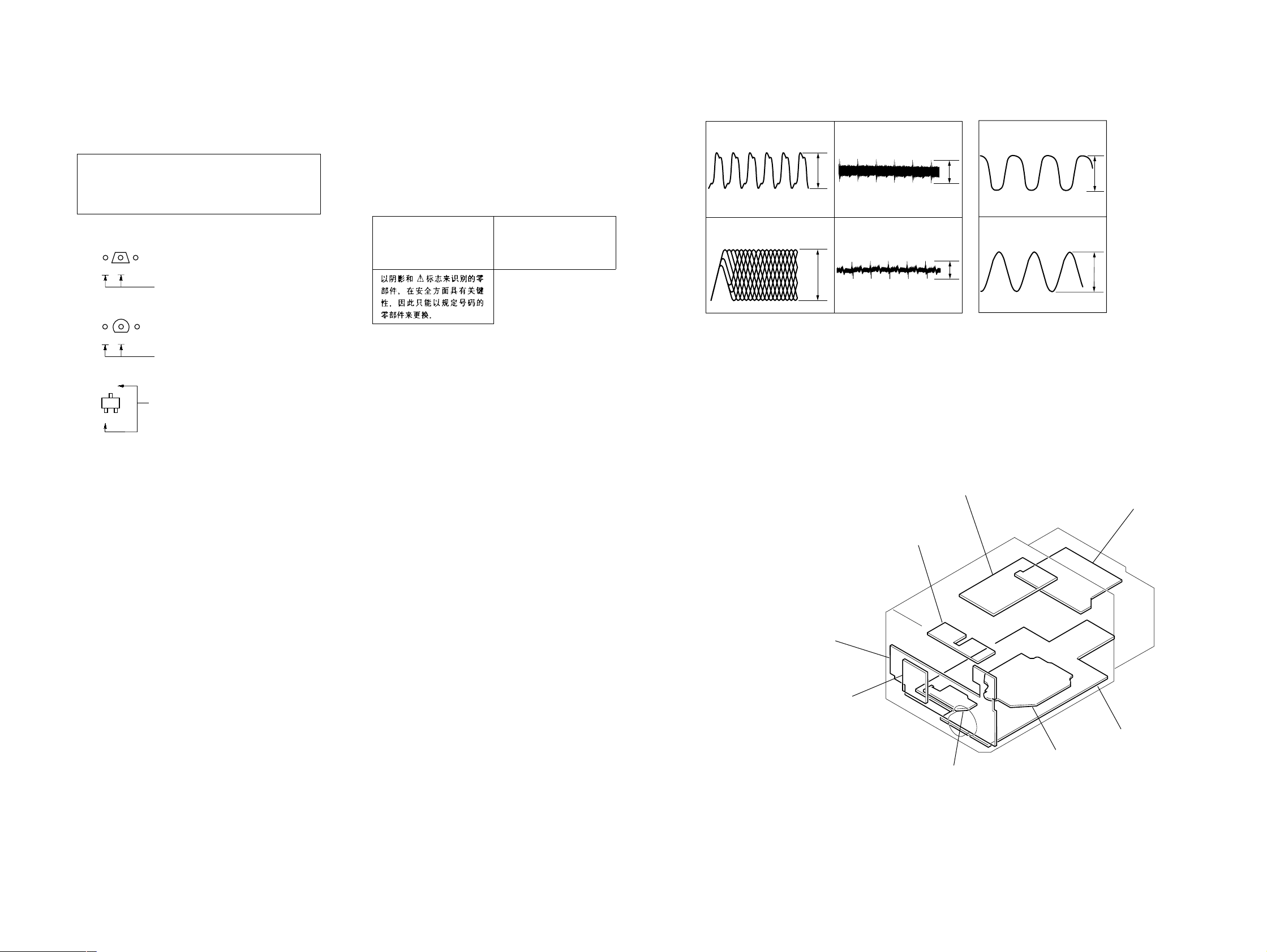
5-1. Wavefoarms
– BD BOARD – – MAIN BOARD –
1
1
IC101 yj
CD PLAY MODE
16.9344MHz
2
IC101 ta
CD PLAY MODE
400nsec/div
3
CD PLAY MODE
6.4Vp-p
4
CD PLAY MODE
1.2Vp-p
IC101 ra
approx 200mVp-p
IC101 el
approx 170mVp-p
IC601 qa
STOP MODE
32.768kHz
2
IC601 qd
STOP MODE
16MHz
5-2. CIRCUIT BOARDS LOCATION
TUNER (FM/AM) UNIT
LED board
PANEL board
3.0Vp-p
3.4Vp-p
BACK PANEL board
H.P. board
MAIN board
BD board
LOADING board
1111
Page 12

HCD-RB5
Ver 1.1 2001.12
5-3. PRINTED WIRING BOARD –BD SECTION–
• Semiconductor
Location
Ref. No. Location
IC101 C-2
IC102 C-3
IC103 B-2
Q101 A-3
• See page 11 for Circuit Boards Location.
TP
(VC)
TP
(RF)
• : Uses unleaded solder.
TP(TE0)
TP(FE0)
TP(FE1)
TP(AGC CON)
TP(D GND)
(Page 14)
TP
(XPCK)
1212
Page 13

HCD-RB5
5-4. SCHEMATIC DIAGRAM –BD SECTION–
• See page 11 for Waveforms.
• See page 22 for IC Block Diagrams.
1313
Page 14

HCD-RB5
Ver 1.1 2001.12
5-5. PRINTED WIRING BOARDS –MAIN SECTION–
• See page 11 for Circuit Boards Location.
(Page 18)
• : Uses unleaded solder.
(Page 12)
There are a few cases that the part printed on
this diagram isn’t mounted in this model.
• Semiconductor Location
Ref. No. Location
D2 D-7
D3 B-8
D4 C-5
D5 C-3
D6 F-7
D7 F-6
D8 E-7
D9 F-7
D10 G-4
D14 D-6
D15 D-6
D16 D-6
D17 E-8
D18 E-7
D19 E-8
D20 E-7
D21 G-5
D321 D-10
D501 B-1
D551 F-5
D552 F-5
D553 F-6
D554 G-3
D555 E-6
D556 E-6
D601 D-4
Ref. No. Location
IC1 G-3
IC2 G-6
IC3 E-6
IC4 F-5
IC201 C-3
IC202 C-2
IC301 D-9
IC501 B-1
IC551 G-4
IC601 E-4
Q1 B-8
Q2 G-5
Q3 G-4
Q4 G-4
Q10 F-5
Q201 C-7
Q202 D-4
Q203 D-4
Q204 D-5
Q251 C-7
Q254 D-5
Q322 D-10
Q323 D-10
Q324 D-10
Q551 G-3
(Page 20)
(Page 17)
(Page 17)
(Page 17)
1414
Page 15

HCD-RB5
5-6. SCHEMATIC DIAGRAM –MAIN SECTION(1/2)–
• See page 11 for Waveforms.
• See page 20 for IC Pin Function.
PIN FUNCTION
1515
Page 16

HCD-RB5
5-7. SCHEMATIC DIAGRAM –MAIN SECTION(2/2)–
• See page 22 for IC Block Diagrams.
1616
Page 17

5-8. PRINTED WIRING BOARDS –POWER SECTION–
(Pag
)
• See page 11 for Circuit Boards Location.
• : Uses unleaded solder.
HCD-RB5
Ver 1.1 2001.12
There are a few cases that the part printed on
this diagram isn’t mounted in this model.
(Page 14)
VOLTAGE
SELECTOR
110-120V
R
220-240V
(Page 14)
e 14
1717
Page 18

HCD-RB5
Ver 1.1 2001.12
5-9. PRINTED WIRING BOARD –PANEL SECTION–
• Semiconductor
Location
Ref. No. Location
D801 A-2
D805 C-6
D806 C-7
IC801 A-1
IC802 C-4
Q801 A-1
Q804 D-6
Q805 C-3
Q806 C-6
Q807 C-6
• See page 11 for Circuit Boards Location.
• : Uses unleaded solder.
There are a few cases that the part printed on
this diagram isn’t mounted in this model.
(Page 14)
Z
1818
Page 19

5-10. SCHEMATIC DIAGRAM –PANEL SECTION–
HCD-RB5
1919
Page 20

HCD-RB5
Ver 1.1 2001.12
5-11. SCHEMATIC DIAGRAM –LOADING SECTION–
• See page 11 for Waveforms.
5-13. IC Pin Function
• MAIN BOARD IC601 M30622MAA-A64FP (SYSTEM CONTROLLER)
S1
LOADING
SWITCH
M103
LOADING
MOTOR
16
5-12. PRINTED WIRING BOARDS –LODING SECTION–
TO MAIN
(Page 14)
16
CN1
CLOSE
GND
OPEN
LOAD +
MAIN BOARD
LOAD –
(Page 16)
• : Uses unleaded solder.
BOARD
B
TO
(3/3)
Pin No.
1
2
3
4
5
6
7
8
9
10
11
12
13
14
15
16
17
18
19
20
21
22
23
24
25
26
27
28
29
30
31
32
33
34
35
36
37
38
39
40
41
42
43
44
45
46
47
48
49
50
Pin Name
STKPOWER
B-SHUT
SPEAKER RELAY
H.PHONE DETECT
CD-POWER
TA-MUTE
LED
BYTE
CNVss
XCIN
XCOUT
RESET
X0UT
VSS
XIN
VCC
NMI
LED
SCOR
RDS-INT
RDS-DATA
AC-CUT
PBC/CDTEXT LED
VCD LED
CDTEXT LED
PANEL LED
PRE MUTE
FL-RESET
IIC_CLK
IIC_DATA
RXD
SQ-DATA-IN
SQ-CLK
RTS1
FL-DATA
FL-CS
FL-CLK
VOL_CLK
STBY LED
TIMER LED
VSS
RECOUT MUTE
STBY_RELAY
AMP_MUTE
AMP_STANDBY
VDD
VOL_DATA
VOL_CLK
ST-MUTE
STEREO
I/O
I
Not used. OPEN
I
Not used. OPEN
O
FRONT-RELAY ON(H)/OFF(L)
I
HEAD PHONEs detection. Connected (H), Not connected (L).
O
CD-POWER ON(H)/OFF(L)
O
Not used. OPEN
—
Not used. OPEN
—
For switching external data bus wedth
—
For switching precessor mode
I
SUB CLOCK IN
O
SUB CLOCK OUT
—
SYSTEM RESET IN
O
MAIN SYSTEM CLOCK OUT
—
Vss
I
MAIN SYSTEM CLOCK IN(16MHz)
—
POWER SUPPLY(+5V)
I
PULL UP(EVER +5V) CAN’T USE
—
Not used. OPEN
I
CD Q-DATA REQUEST
I
RDS INT
I
RDS DATA
I
AC CUT ON(L)/OFF(H) CHECK
O
CDTEXT LED (RB5) / PBC LED (VB5)
O
VCD_LED
O
Not used. OPEN
O
PANEL_LED
O
TA LINE-MUTE ON(L)/OFF(H)
O
FL RESET
I
IIC SCL
I
IIC SDA
—
Not used. OPEN
O
CD DATA IN
I
Note: SQ CLK : Input when CD-POWER is L
O
Not used. OPEN
O
FL DATA
O
FL CHIP SELECT
O
FL CLK
O
LC75342 LATCH
O
STANDBY LED
O
TIMER LED
—
FLASH VSS
—
FL FILAMENT ON(H)/OFF(L) (for ECO)
O
Always O/H when power is OFF except for J, U and CED
I
Always O/H when power is OFF except for J, U and CED
I
Always O/H when power is OFF except for J, U and CED
—
FLASH VDD
O
LC75342 DATA
O
LC75342 CLOCK
O
TUNER MUTE
I
STEREO IN(L)/OFF(H)
Description
2020
Page 21

Pin No.
51
52
53
54
55
56
57
58
59
60
61
62
63
64
65
66
67
68
69
70
71
72
73
74
75
76
77
78
79
80
81
82
83
84
85
86
87
88
89
90
91
92
93
94
95
96
97
98
99
100
Pin Name
TUNED
ST-CE
ST-DOUT
ST-DIN
ST-CLK
SENS
HOLD
XLTAT
XRST
LED
LED
VCC
LED
VSS
AMS-IN
LOAD-OUT
LOAD-IN
B-TRG
CAPM-CNT1
IN SW
OPEN-SW
TC-MUTE
REC/PB/PASS
DOLBY NR
REC-MUTE
BIAS
EQ-H/N
TC-RELAY
ALC
B-PLAY-SW
CD-DATA
CD-CLK
REC-OUT
JOG A
JOG B
ENC A
ENC B
SIRCS
KEY0
KEY1
KEY2
MD REC R
B-HALF
MD REC L
MODEL-IN
AVSS
SPEC-IN
VREF
AVCC
TEST
I/O
I
TUNED IN(L)/OFF(H)
O
TUNER CHIP ENB
O
TUNER DATA OUT
I
TUNER DATA IN
O
TUNER CLOCK
I
From CXP2587 SENS
O
MODE
O
CD LAT
O
CD RESET
O
Not used. OPEN
O
Not used. OPEN
—
POWER SUPPLY(+5V)
O
Not used. OPEN
—
Vss
I
Not used. OPEN
O
LOAD OUT
O
LOAD IN
I
Not used. OPEN
I
Not used. OPEN
I
CDM55 IN SW
I
TRAY OPEN switch
I
Not used. OPEN
I
Not used. OPEN
I
Not used. OPEN
I
Not used. OPEN
I
Not used. OPEN
I
Not used. OPEN
I
Not used. OPEN
I
Not used. OPEN
I
Not used. OPEN
O
CD DATA
O
CD CLK
I
Not used. OPEN
I
Not used. OPEN
I
Not used. OPEN
I
volume(A)
I
volume(B)
I
remote commander input
I
KEY-line(0)
I
KEY-line(1)
I
KEY-line(2)
I
Not used. OPEN
I
Not used. OPEN
I
Not used. OPEN
I
CMT-RB5(GND) / CMT-VB5(Vdd)
—
Analog ground
I
SPEC IN
—
Analog Reference Voltage
—
Analog Power Supply
O
SOFT CHECK OUT
Description
21
Page 22

5-14. IC BLOCK DIAGRAMS
— BD BOARD —
IC101 CXD2587Q
LRCK
PCMD
BCK
EMPH
XVDD
XTAI
XTAO
XVSS
AVDD1
AOUT1
AIN1
LOUT1
AVSS1
AVSS2
LOUT2
AIN2
AOUT2
AVDD2
RMUT
LMUT
VDD
AVDD3
DOUT
60
DIGITAL
OUT
61
62
63
64
65
66
67
68
69
70
71
72
73
74
75
76
77
78
79
80
D/A
INTERFACE
TIMING
LOGIC
OVER SAMPLING
PWM
3rd ORDER
NOISE SHAPER
DIGITAL FILTER
SERIAL IN
INTERFACE
59
58
INTERNAL BUS
PWM
VSS
57
ERROR
CORRECTOR
16K
RAM
SUBCODE
PROCESSOR
FILO
FILI
PCO
54
56
55
53
DIGITAL
PLL
EFM
DEMODULATOR
SERVO
INTERFACE
SERVO AUTO
SEQUENCER
CLTV
AVSS3
52
ASYI
BIAS
RFAC
51
49
50
ASYMMETRY
CORRECTION
48
ASYO
47
AVDD0
46
IGEN
45
AVSS0
ADIO
44
SERVO DSP
FOCUS
SERVO
TRACKING
SERVO
SLED
SERVO
CE
TE
RFDC
43
41
42
OPERATIONAL
AMPLIFIER
ANALOG SWITCH
A/D
CONVERTER
PWM GENERATOR
CLOCK
GENERATOR
FOCUS PWM
GENERATOR
TRACKING
PWM GENERATOR
SLED PWM
GENERATOR
DIGITAL
CLV
MIRR, DFCT,
FOK
DETECTOR
SE
40
FE
39
VC
38
XTSL
37
TES1
36
TEST
35
VSS
34
33
FRDR
32
FFDR
TRDR
31
TFDR
30
SRDR
29
28
SFDR
SSTP
27
MDP
26
25
LOCK
FOK
24
DFCT
23
22
MIRR
3
1
2
SQSO
SQCK
XRST
4
SYSM
— MAIN BOARD —
IC501 LB1641
T.S.D O.C.P
1
GND
MOTOR
DRIVE
2 3
DRIVE
MOTOR
NOISE
FILTER
CPU
INTERFACE
5
4
CLAMP
6
DATA
7
XLAT
FWD/REV/STOP
CONTROL LOGIC
9
10
8
SENS
CLOK
5 6 7 8 9
FWD.IN
SCLK
REV.IN
11 12
VDD
ATSK
SPOA
VCC 1
13
14
XLON
SPOB
1516171819
XUGF
XPCK
WFCK
MOTOR
VCC 2
NOISE
FILTER
GFS
DRIVE
20
C2PO
10
MOTOR
SCOR
DRIVE
COUT
21
22
Page 23

NOTE:
• -XX, -X mean standardized parts, so they may
have some differences from the original one.
• Items marked “*” are not stocked since they
are seldom required for routine service. Some
delay should be anticipated when ordering these
items.
• The mechanical parts with no reference number
in the exploded views are not supplied.
• Hardware (# mark) list and accessories and
packing materials are given in the last of this
parts list.
6-1. CASE(TOP) SECTION
SECTION 6
EXPLODED VIEWS
• Abbreviation
CND : Canadian model.
AUS : Australian model.
SP : Singapore model.
MY : Malaysia model.
AR : Argentine model.
AED : North European model.
MX : Mexican model.
KR : Korean model.
EE : East European model.
HK : Hong Kong model.
TW : Taiwan model.
CH : Chinese model.
The components identified by mark 0 or
dotted line with mark 0 are critical for safety.
Replace only with part number specified.
Les composants identifiés par une marque
0 sont critiques pour la sécurité.
Ne les remplacer que par une pièce portant
le numéro spécifié.
3
#1
5
#1
4
#1
6
#1
2
2
#1
1
#1
7
#2
4
Ref. No. Part No. Description Remarks Ref. No. Part No. Description Remarks
1 4-230-227-01 PLATE (TOP), ORNAMENTAL
2 4-230-228-01 SCREW (TOP)
3 4-230-225-01 CASE (LEFT)
4 3-363-099-21 SCREW (CASE 3 TP2)
5 4-230-224-01 CASE (TOP)
6 4-230-222-01 PANEL, BACK (AEP,UK,AED,EE,CIS,CH)
6 4-230-222-11 PANEL, BACK (US,CND,MX,KR,AUS)
6 4-230-222-21 PANEL, BACK (E,AR,HK,SP,MY,TW)
7 4-230-226-01 CASE (RIGHT)
23
Page 24

6-2. FRONT PANEL SECTION
Supplied with MAIN board.
z
A : PANEL board
z
B : LED board
z
C : H.P. board
54
z
C
55
z
B
z
A
51
52
53
54
54
not
supplied
54
56
Ref. No. Part No. Description Remarks Ref. No. Part No. Description Remarks
51 4-230-213-01 WINDOW (TOP)
(US,CND,E,MX,AR,HK,SP,MY,KR,TW,AUS,CH)
51 4-230-213-11 WINDOW (TOP) (AEP,UK,AED,EE,CIS)
52 4-230-202-01 KNOB (MAIN)
53 X-4953-261-1 PANEL ASSY, FRONT
54 4-951-620-01 SCREW (2.6X8), +BVTP
55 4-933-134-11 SCREW (+PTPWH M2.6X8)
56 1-765-343-11 WIRE (FLAT TYPE) (23 CORE)
24
Page 25

6-3. CHASSIS SECTION
d
Supplied with MAIN board.
z
D : BACK PANEL board
101
#4
not supplied
102
115
CDM55C-K6BD38
not supplied
#2
not supplied
#2
107
#2
108
#3
104
103
110
#2
#3
#2
105
#2
not supplied
106
#2
116
not supplied
#2
z
113
#2
D
#2
not supplied
#2
111
not supplie
T901
not supplied
#2
not supplied
Ref. No. Part No. Description Remarks Ref. No. Part No. Description Remarks
101 4-230-206-01 PANEL, LOADING
102 1-693-481-11 TUNER (FM/AM) (US,CND)
102 1-693-482-11 TUNER (FM/AM) (HK,SP,MY,KR,TW,AUS)
102 1-693-484-11 TUNER (FM/AM) (E,MX,AR)
102 1-693-490-11 TUNER (FM/AM) (AEP,UK,AED,EE,CIS,CH)
103 1-757-267-11 WIRE, FLAT TYPE (19 CORE)
104 1-757-266-11 WIRE, FLAT TYPE (13 CORE)
105 1-769-980-11 WIRE (FLAT TYPE) (13 CORE)
(US,CND,E,MX,AR,HK,SP,MY,KR,TW,AUS,CH)
105 1-773-013-11 WIRE (FLAT TYPE) (15 CORE)
(AEP,UK,AED,EE,CIS)
106 3-703-244-00 BUSHING (2104), CORD (EXCEPT E,MX)
* 106 3-703-571-12 BUSHING (S) (4516), CORD (E,MX)
107 3-704-515-11 SCREW (BV/RING)
108 A-4475-310-A MAIN BOARD, COMPLETE (US,CND)
108 A-4475-315-A MAIN BOARD, COMPLETE (AEP,UK,AED,EE,CIS)
108 A-4475-320-A MAIN BOARD, COMPLETE (E,MX,AR)
108 A-4475-322-A MAIN BOARD, COMPLETE
(HK,SP,MY,KR,TW,AUS)
#4
108 A-4475-497-A MAIN BOARD, COMPLETE (CH)
109 4-965-822-01 FOOT
110 3-970-608-01 SCREW SUMITITE(B3), +BV
* 111 3-743-347-01 COVER, FUSE
* 113 4-374-846-21 COVER, CAPACITOR, CAP TYPE_HCDRB5
115 3-531-576-01 RIVET
0 116 1-775-787-41 CORD, POWER
0 116 1-775-790-41 CORD, POWER (AUS)
0 116 1-783-531-31 CORD, POWER (US,CND)
0 116 1-783-941-31 CORD, POWER (AR)
0 116 1-791-686-11 CORD, POWER (CH)
0 116 1-792-382-21 CORD, POWER (E,MX)
0 116 1-769-079-11 CORD, POWER (KR)
0 T901 1-435-652-11 TRANSFORMER, POWER (US,CND,MX)
0 T901 1-435-653-11 TRANSFORMER, POWER
0 T901 1-435-654-11 TRANSFORMER, POWER
109
(AEP,UK,AED,EE,CIS,HK,SP,MY,TW)
(E,AR,HK,SP,MY,TW,CH)
(AEP,UK,AED,EE,CIS,KR,AUS)
The components identified by
mark 0 or dotted line with mark
0 are critical for safety.
Replace only with part number
specified.
Les composants identifiés par
une marque 0 sont critiques
pour la sécurité.
Ne les remplacer que par une
pièce portant le numéro spécifié.
25
Page 26

6-4. CD MECHANISM DECK SECTION
(CDM55C-K6BD38)
154
159
161
152
M901
153
157
164
158
155
156
165
160
not supplied
162
151
BU-K6BD38
163
Ref. No. Part No. Description Remarks Ref. No. Part No. Description Remarks
151 4-224-894-11 TRAY (CDM55D)
152 4-220-229-01 LEVER (SW)
153 4-220-239-11 SPRING, TORSION
154 4-221-816-11 BELT (CDM55)
155 4-220-234-01 PULLEY (LDG)
156 4-220-238-01 GEAR (B)
157 4-220-237-01 GEAR (A)
158 4-220-233-01 CAM (CDM55)
159 1-674-336-21 LOADING BOARD
160 4-221-815-01 ROLLER
161 7-685-534-19 SCREW +BTP 2.6X8 TYPE2 N-S
162 X-4953-195-1 PULLEY (AT) ASSY
163 4-985-672-01 SCREW (+PTPWHM2.6), FLOATING
164 4-227-598-01 SPACER (55)
164 1-452-925-21 MAGNET ASSY
M901 A-4672-771-A MOTOR (LD) ASSY (LOADING)
26
Page 27

6-5. BASE UNIT SECTION (BU-K6BD38)
201
202
201
201
204
203
205
202
202
201
202
208
206
206
207
Ref. No. Part No. Description Remarks Ref. No. Part No. Description Remarks
201 4-985-672-01 SCREW (+PTPWHM2.6), FLOATING
202 4-227-679-01 INSULATOR (213)
0 203 8-820-116-01 OPTICAL PICK-UP KSM-213DCP/Z-NP
204 A-4724-934-A BD BOARD, COMPLETE
206
205 1-792-024-11 WIRE (FLAT TYPE) (16 CORE)
206 4-229-806-01 SPRING (213), COMPRESSION
207 X-4953-169-1 HOLDER (BU) ASSY
208 4-951-620-01 SCREW (2.6X8), +BVTP
206
The components identified by
mark 0 or dotted line with mark
0 are critical for safety.
Replace only with part number
specified.
Les composants identifiés par
une marque 0 sont critiques
pour la sécurité.
Ne les remplacer que par une
pièce portant le numéro spécifié.
27
Page 28

SECTION 7
BACK PANEL
NOTE:
• Due to standardization, replacements in the
parts list may be different from the parts
specified in the diagrams or the components
used on the set.
• -XX, -X mean standardized parts, so they
may have some difference from the original
one.
• Items marked “*” are not stocked since they
are seldom required for routine service.
Some delay should be anticipated when
ordering these items.
• RESISTORS
All resistors are in ohms.
METAL: metal-film resistor
MET AL OXIDE: Metal Oxide-f ilm resistor
F: nonflammable
Ref. No. Part No. Description Remarks Ref. No. Part No. Description Remarks
1-533-293-11 FUSE HOLDER
0 C1 1-113-925-11 CERAMIC 0.01uF 20.00% 250V
C101 1-162-282-31 CERAMIC 100PF 10% 50V
C102 1-162-282-31 CERAMIC 100PF 10% 50V
C103 1-104-665-11 ELECT 100uF 20.00% 10V
C105 1-164-159-11 CERAMIC 0.1uF 50V
BD
BACK PANEL BOARD
*****************
< CAPACITOR >
(US,CND,AEP,UK,AED,EE,CIS)
ELECTRICAL PARTS LIST
• Abbreviation
CND : Canadian model.
AUS : Australian model.
SP : Singapore model.
MY : Malaysia model.
AR : Argentine model.
AED : North European model.
MX : Mexican model.
KR : Korean model.
EE : East European model.
HK : Hong Kong model.
TW : Taiwan model.
CH : Chinese model.
• CAPACITORS:
uF: µF
• COILS
uH: µH
(Supplied with MAIN board)
0 R1 1-202-725-00 SOLID 3.3M 10% 1/2W
R101 1-249-417-11 CARBON 1K 5% 1/4W F
R102 1-249-441-11 CARBON 100K 5% 1/4W
R151 1-249-417-11 CARBON 1K 5% 1/4W F
R152 1-249-441-11 CARBON 100K 5% 1/4W
0 RY1 1-755-276-11 RELAY, POWER (US,CND,AEP,UK,AED,EE,CIS)
• SEMICONDUCTORS
In each case, u: µ, for example:
uA...: µA... , uPA... , µPA... ,
uPB... , µPB... , uPC... , µPC... ,
uPD..., µPD...
When indicating parts by reference number,
please include the board name.
The components identified by mark 0 or
dotted line with mark 0 are critical for safety.
Replace only with part number specified.
Les composants identifiés par une marque
0 sont critiques pour la sécurité.
Ne les remplacer que par une pièce portant
le numéro spécifié.
< RESISTOR >
(US,CND)
< RELAY >
< SWITCH >
C107 1-164-159-11 CERAMIC 0.1uF 50V
C108 1-164-159-11 CERAMIC 0.1uF 50V
C151 1-162-282-31 CERAMIC 100PF 10% 50V
C152 1-162-282-31 CERAMIC 100PF 10% 50V
< CONNECTOR >
CN1 1-774-108-11 PIN, CONNECTOR (PC BOARD)
CN2 1-564-321-00 PIN, CONNECTOR 2P
(US,CND,AEP,UK,AED,EE,CIS,MX,KR,AUS)
* CN2 1-564-687-11 PIN, CONNECTOR 3P(E,AR,HK,SP,MY,TW,CH)
* CN3 1-564-321-21 PIN, CONNECTOR 2P
(US,CND,AEP,UK,AED,EE,CIS)
CN101 1-784-735-11 CONNECTOR, FFC 13P
< DIODE >
D1 8-719-911-19 DIODE 1SS133T-72
(US,CND,AEP,UK,AED,EE,CIS)
< FUSE >
0 F1 1-532-389-51 FUSE TIME-LAG 0.5A/250V (MX)
0 F1 1-532-467-51 FUSE TIME-LAG 0.315A/250V
(AEP,UK,AED,EE,CIS,KR,AUS)
0 F1 1-532-500-51 FUSE, CYLINDRICAL (TIME-LAG) 0.63A/250V
(E,AR,HK,SP,MY,TW,CH)
0 F1 1-533-689-11 FUSE, GLASS CYLINDRICAL(DIA.5)1A/125V
(US,CND)
< IC >
IC101 8-749-923-04 IC TOTX178A (CD DIGITAL OUT OPTICAL)
< JACK >
J101 1-766-851-11 JACK, PIN 4P (MD/VIDEO (AUDIO))
0 S1 1-762-753-11 SWITCH, VOLTAGE SELECTION
(VOLTAGE SELECT) (E,AR,HK,SP,MY,TW)
**************************************************************
A-4724-934-A BD BOARD, COMPLETE
*******************
< CAPACITOR >
C101 1-163-005-11 CERAMIC CHIP 470PF 10% 50V
C102 1-164-004-11 CERAMIC CHIP 0.1uF 10% 25V
C103 1-163-005-11 CERAMIC CHIP 470PF 10% 50V
C104 1-163-009-11 CERAMIC CHIP 0.001uF 10% 50V
C108 1-164-004-11 CERAMIC CHIP 0.1uF 10% 25V
C109 1-163-011-11 CERAMIC CHIP 0.0015uF 10% 50V
C110 1-164-182-11 CERAMIC CHIP 0.0033uF 10% 50V
C111 1-163-251-11 CERAMIC CHIP 100PF 5.00% 50V
C112 1-107-682-11 CERAMIC CHIP 1uF 10.00% 16V
C114 1-163-038-11 CERAMIC CHIP 0.1uF 25V
C115 1-104-665-11 ELECT 100uF 20.00% 10V
C116 1-104-665-11 ELECT 100uF 20.00% 10V
C117 1-104-665-11 ELECT 100uF 20.00% 10V
C118 1-163-009-11 CERAMIC CHIP 0.001uF 10% 50V
C119 1-163-235-11 CERAMIC CHIP 22PF 5.00% 50V
C121 1-163-038-11 CERAMIC CHIP 0.1uF 25V
C122 1-104-665-11 ELECT 100uF 20.00% 10V
C123 1-163-021-91 CERAMIC CHIP 0.01uF 10.00% 50V
C124 1-107-823-11 CERAMIC CHIP 0.47uF 10.00% 16V
C125 1-163-038-11 CERAMIC CHIP 0.1uF 25V
C126 1-163-038-11 CERAMIC CHIP 0.1uF 25V
C127 1-104-665-11 ELECT 100uF 20.00% 10V
C129 1-163-031-11 CERAMIC CHIP 0.01uF 50V
C130 1-164-346-11 CERAMIC CHIP 1uF 16V
C131 1-126-964-11 ELECT 10uF 20.00% 50V
28
Page 29

BD
Ref. No. Part No. Description Remarks Ref. No. Part No. Description Remarks
C133 1-164-346-11 CERAMIC CHIP 1uF 16V
C140 1-164-346-11 CERAMIC CHIP 1uF 16V
C141 1-164-346-11 CERAMIC CHIP 1uF 16V
C143 1-163-038-11 CERAMIC CHIP 0.1uF 25V
C145 1-163-038-11 CERAMIC CHIP 0.1uF 25V
R158 1-216-111-00 METAL CHIP 390K 5% 1/10W
R159 1-216-101-00 METAL CHIP 150K 5% 1/10W
R162 1-216-101-00 METAL CHIP 150K 5% 1/10W
R171 1-216-078-00 RES-CHIP 16K 5% 1/10W
R172 1-216-073-00 METAL CHIP 10K 5% 1/10W
H.P. LODAINGLED
C153 1-163-038-11 CERAMIC CHIP 0.1uF 25V
C159 1-163-019-00 CERAMIC CHIP 0.0068uF 10% 50V
C162 1-104-665-11 ELECT 100uF 20.00% 10V
C163 1-104-665-11 ELECT 100uF 20.00% 10V
C165 1-163-038-11 CERAMIC CHIP 0.1uF 25V
C167 1-163-237-11 CERAMIC CHIP 27PF 5.00% 50V
C168 1-163-235-11 CERAMIC CHIP 22PF 5.00% 50V
C171 1-163-009-11 CERAMIC CHIP 0.001uF 10% 50V
C172 1-163-123-00 CERAMIC CHIP 180PF 5% 50V
C181 1-163-009-11 CERAMIC CHIP 0.001uF 10% 50V
C182 1-163-123-00 CERAMIC CHIP 180PF 5% 50V
< CONNECTOR >
CN101 1-784-741-11 CONNECTOR, FFC 19P
CN102 1-793-907-11 CONNECTOR, FFC/FPC 16P
< FERRITE BEAD >
FB101 1-469-731-21 INDUCTOR 0UH
FB103 1-469-731-21 INDUCTOR 0UH
< IC >
IC101 8-752-386-85 IC CXD2587Q
IC102 8-759-549-28 IC BA5974FP-E2
IC103 8-752-085-51 IC CXA2568M-T6
< TRANSISTOR >
Q101 8-729-010-08 TRANSISTOR MSB710-RT1
R173 1-216-077-91 RES-CHIP 15K 5% 1/10W
R181 1-216-078-00 RES-CHIP 16K 5% 1/10W
R182 1-216-073-00 METAL CHIP 10K 5% 1/10W
R183 1-216-077-91 RES-CHIP 15K 5% 1/10W
< NETWORK >
RN101 1-233-576-11 RES, CHIP NETWORK 100
< SWITCH >
S101 1-771-853-11 SWITCH, DETECTION (LIMIT IN)
< VIBRATOR >
X101 1-579-280-11 VIBRATOR, CRYSTAL 16.9344MHz
**************************************************************
H.P. BOARD
*********
(Supplied with MAIN board)
< CAPACITOR >
C901 1-162-294-31 CERAMIC 0.001uF 10% 50V
C902 1-162-294-31 CERAMIC 0.001uF 10% 50V
C903 1-164-159-11 CERAMIC 0.1uF 50V
C951 1-162-294-31 CERAMIC 0.001uF 10% 50V
< JACK >
J901 1-785-569-11 JACK (SMALL TYPE) (PHONES)
**************************************************************
< RESISTOR >
R101 1-216-077-91 RES-CHIP 15K 5% 1/10W
R102 1-216-097-11 RES-CHIP 100K 5% 1/10W
R103 1-216-077-91 RES-CHIP 15K 5% 1/10W
R104 1-216-085-00 METAL CHIP 33K 5% 1/10W
R105 1-216-073-00 METAL CHIP 10K 5% 1/10W
R106 1-216-049-11 RES-CHIP 1K 5% 1/10W
R107 1-216-073-00 METAL CHIP 10K 5% 1/10W
R108 1-216-061-00 METAL CHIP 3.3K 5% 1/10W
R109 1-216-121-11 RES-CHIP 1M 5% 1/10W
R110 1-216-025-11 RES-CHIP 100 5% 1/10W
R111 1-216-121-11 RES-CHIP 1M 5% 1/10W
R113 1-216-121-11 RES-CHIP 1M 5% 1/10W
R114 1-216-073-00 METAL CHIP 10K 5% 1/10W
R116 1-216-001-00 METAL CHIP 10 5% 1/10W
R117 1-216-049-11 RES-CHIP 1K 5% 1/10W
R118 1-216-025-11 RES-CHIP 100 5% 1/10W
R119 1-216-059-00 METAL CHIP 2.7K 5% 1/10W
R123 1-216-073-00 METAL CHIP 10K 5% 1/10W
R124 1-216-097-11 RES-CHIP 100K 5% 1/10W
R131 1-216-033-00 METAL CHIP 220 5% 1/10W
R143 1-216-103-00 METAL CHIP 180K 5% 1/10W
R144 1-216-103-00 METAL CHIP 180K 5% 1/10W
R147 1-216-069-00 METAL CHIP 6.8K 5% 1/10W
R148 1-216-001-00 METAL CHIP 10 5% 1/10W
R149 1-216-001-00 METAL CHIP 10 5% 1/10W
LED BOARD
**********
(Supplied with MAIN board)
< DIODE >
D803 8-719-071-41 DIODE SELS5923C-TP15
D804 8-719-071-41 DIODE SELS5923C-TP15
**************************************************************
1-674-336-21 LOADING BOARD
**************
< CONNECTOR >
* CN1 1-568-943-11 PIN, CONNECTOR 5P
< SWITCH >
S1 1-771-799-11 SWITCH, LEVER (SLIDE) (LOADING)
**************************************************************
29
Page 30

MAIN
Ref. No. Part No. Description Remarks Ref. No. Part No. Description Remarks
A-4475-310-A MAIN BOARD, COMPLETE (US,CND)
*********************
A-4475-315-A MAIN BOARD, COMPLETE (AEP,UK,AED,EE,CIS)
*********************
A-4475-320-A MAIN BOARD, COMPLETE (E,MX,AR)
*********************
A-4475-322-A MAIN BOARD, COMPLETE
*********************(HK,SP,MY,KR,TW,AUS)
A-4475-497-A MAIN BOARD, COMPLETE (CH)
*********************
C251 1-126-964-11 ELECT 10uF 20.00% 50V
C252 1-136-172-00 MYLAR 0.39uF 5.00% 50V
C253 1-136-165-00 MYLAR 0.1uF 5.00% 50V
C254 1-130-476-00 MYLAR 0.0027uF 5% 50V
C256 1-126-964-11 ELECT 10uF 20.00% 50V
C257 1-126-963-11 ELECT 4.7uF 20.00% 50V
C265 1-126-963-11 ELECT 4.7uF 20.00% 50V
C266 1-126-963-11 ELECT 4.7uF 20.00% 50V
C267 1-126-963-11 ELECT 4.7uF 20.00% 50V
C269 1-126-964-11 ELECT 10uF 20.00% 50V
< CAPACITOR >
C2 1-136-165-00 FILM 0.1uF 5.00% 50V
C3 1-136-165-00 FILM 0.1uF 5.00% 50V
C4 1-128-548-11 ELECT 4700uF 20.00% 25V
C5 1-126-948-11 ELECT 100uF 20.00% 35V
C6 1-161-494-00 CERAMIC 0.022uF 25V
C7 1-126-933-11 ELECT 100uF 20.00% 16V
C8 1-136-165-00 FILM 0.1uF 5.00% 50V
C9 1-136-165-00 FILM 0.1uF 5.00% 50V
C10 1-126-768-11 ELECT 2200uF 20.00% 16V
C11 1-104-665-11 ELECT 100uF 20.00% 25V
C12 1-104-664-11 ELECT 47uF 20.00% 25V
C13 1-161-494-00 CERAMIC 0.022uF 25V
C15 1-104-664-11 ELECT 47uF 20.00% 25V
C16 1-128-551-11 ELECT 22uF 20.00% 25V
C17 1-104-664-11 ELECT 47uF 20.00% 25V
C18 1-128-551-11 ELECT 22uF 20.00% 25V
C19 1-126-965-11 ELECT 22uF 20.00% 50V
C20 1-126-965-11 ELECT 22uF 20.00% 50V
C21 1-126-967-11 ELECT 47uF 20.00% 50V
C22 1-164-159-11 CERAMIC 0.1uF 50V
C23 1-126-951-11 ELECT 470uF 20.00% 35V
C24 1-126-963-11 ELECT 4.7uF 20.00% 50V
(US,CND,AEP,UK,AED,EE,CIS)
C25 1-136-165-00 FILM 0.1uF 5.00% 50V
(US,CND,AEP,UK,AED,EE,CIS)
C26 1-136-165-00 FILM 0.1uF 5.00% 50V
(US,CND,AEP,UK,AED,EE,CIS)
C27 1-126-767-11 ELECT 1000uF 20.00% 16V
C28 1-128-551-11 ELECT 22uF 20.00% 25V
C29 1-126-967-11 ELECT 47uF 20.00% 50V
C30 1-164-159-11 CERAMIC 0.1uF 50V
C54 1-128-548-11 ELECT 4700uF 20.00% 25V
C201 1-126-964-11 ELECT 10uF 20.00% 50V
C202 1-136-172-00 MYLAR 0.39uF 5.00% 50V
C203 1-136-165-00 MYLAR 0.1uF 5.00% 50V
C204 1-130-476-00 MYLAR 0.0027uF 5% 50V
C206 1-126-964-11 ELECT 10uF 20.00% 50V
C207 1-126-963-11 ELECT 4.7uF 20.00% 50V
C208 1-162-294-31 CERAMIC 0.001uF 10% 50V
C209 1-126-935-11 ELECT 470uF 20.00% 16V
C210 1-161-494-00 CERAMIC 0.022uF 25V
C211 1-128-551-11 ELECT 22uF 20.00% 25V
C214 1-107-715-11 ELECT 22uF 20.00% 16V
C215 1-126-963-11 ELECT 4.7uF 20.00% 50V
C216 1-126-963-11 ELECT 4.7uF 20.00% 50V
C217 1-126-963-11 ELECT 4.7uF 20.00% 50V
C219 1-126-964-11 ELECT 10uF 20.00% 50V
C221 1-162-290-31 CERAMIC 470PF 10% 50V
C271 1-162-290-31 CERAMIC 470PF 10% 50V
C302 1-161-494-00 CERAMIC 0.022uF 25V
C303 1-126-047-71 ELECT 4.7uF 20.00% 50V
C305 1-126-022-11 ELECT 47uF 20.00% 25V
C306 1-163-123-00 CERAMIC 180PF 5.00% 50V
C307 1-164-159-11 CERAMIC 0.1uF 50V
C308 1-164-159-11 CERAMIC 0.1uF 50V
C309 1-164-159-11 CERAMIC 0.1uF 50V
C310 1-164-159-11 CERAMIC 0.1uF 50V
C314 1-162-219-31 CERAMIC 68PF 5.00% 50V
C321 1-126-933-11 ELECT 100uF 20.00% 16V
C322 1-126-967-11 ELECT 47uF 20.00% 50V
C323 1-164-159-11 CERAMIC 0.1uF 50V
C352 1-161-494-00 CERAMIC 0.022uF 25V
C353 1-126-047-71 ELECT 4.7uF 20.00% 50V
C355 1-126-022-11 ELECT 47uF 20.00% 25V
C356 1-163-123-00 CERAMIC 180PF 5.00% 50V
C357 1-164-159-11 CERAMIC 0.1uF 50V
C358 1-164-159-11 CERAMIC 0.1uF 50V
C359 1-164-159-11 CERAMIC 0.1uF 50V
C360 1-164-159-11 CERAMIC 0.1uF 50V
C364 1-162-219-31 CERAMIC 68PF 5.00% 50V
C415 1-164-159-11 CERAMIC 0.1uF 50V
C419 1-162-300-11 CERAMIC 10000PF
C417 1-126-917-11 ELECT 3300uF 20.00% 6.3V
C418 1-126-928-11 ELECT 3300uF 20.00% 10V
C431 1-126-935-11 ELECT 470uF 20.00% 16V
C435 1-126-935-11 ELECT 470uF 20.00% 6.3V
(AEP,UK,AED,EE,CIS)
C501 1-162-306-11 CERAMIC 0.01uF 30.00% 16V
C502 1-162-306-11 CERAMIC 0.01uF 30.00% 16V
C503 1-162-306-11 CERAMIC 0.01uF 30.00% 16V
C504 1-126-933-11 ELECT 100uF 20.00% 16V
C507 1-126-933-11 ELECT 100uF 20.00% 16V
C551 1-128-835-91 ELECT 1000uF 20% 10V
C552 1-104-664-11 ELECT 47uF 20.00% 16V
C553 1-164-159-11 CERAMIC 0.1uF 50V
C554 1-104-664-11 ELECT 47uF 20.00% 16V
C555 1-164-159-11 CERAMIC 0.1uF 50V
C556 1-164-159-11 CERAMIC 0.1uF 50V
C558 1-126-961-11 ELECT 2.2uF 20.00% 50V
C601 1-162-306-11 CERAMIC 0.01uF 30.00% 16V
C602 1-162-205-31 CERAMIC 18PF 5% 50V
C603 1-162-205-31 CERAMIC 18PF 5% 50V
C604 1-161-494-00 CERAMIC 0.022uF 25V
C605 1-161-494-00 CERAMIC 0.022uF 25V
C606 1-161-494-00 CERAMIC 0.022uF 25V
C607 1-161-494-00 CERAMIC 0.022uF 25V
C608 1-162-282-31 CERAMIC 100PF 10% 50V
C609 1-162-282-31 CERAMIC 100PF 10% 50V
C610 1-162-282-31 CERAMIC 100PF 10% 50V
30
Page 31

MAIN
Ref. No. Part No. Description Remarks Ref. No. Part No. Description Remarks
C611 1-126-934-11 ELECT 220uF 20.00% 10V
C612 1-126-916-11 ELECT 1000uF 20.00% 6.3V
C613 1-164-159-11 CERAMIC 0.1uF 50V
< CONNECTOR >
IC202 8-759-634-51 IC M5218AP
IC301 8-759-333-24 IC LM1876TF
IC501 8-759-822-09 IC LB1641
IC551 8-759-635-63 IC M51943BSL-TP
IC601 8-759-679-09 IC M30622MAA-A64FP
* CN4 1-564-510-11 PLUG, CONNECTOR 7P
CN5 1-564-321-21 PIN, CONNECTOR 2P (US,CND,AEP,UK,AED,EE,CIS)
CN201 1-784-774-11 CONNECTOR, FFC 13P
CN202 1-506-469-11 PIN, CONNECTOR 4P
CN401 1-784-780-11 CONNECTOR, FFC 19P
CN421 1-784-774-11 CONNECTOR, FFC 13P
(US,CND,E,MX,AR,HK,SP,MY,KR,TW,AUS,CH)
CN421 1-784-776-11 CONNECTOR, FFC 15P (AEP,UK,AED,EE,CIS)
CN441 1-784-784-11 CONNECTOR, FFC 23P
* CN601 1-764-333-11 PLUG, CONNECTOR 10P
< DIODE >
D2 8-719-500-56 DIODE D3SBA20
D3 8-719-935-69 DIODE HZS11B1LTA
D4 8-719-200-82 DIODE 11ES2-TA2B
D5 8-719-200-82 DIODE 11ES2-TA2B
D6 8-719-975-85 DIODE 21DQ04-TA2
D7 8-719-975-85 DIODE 21DQ04-TA2
D8 8-719-975-85 DIODE 21DQ04-TA2
D9 8-719-975-85 DIODE 21DQ04-TA2
D10 8-719-933-35 DIODE HZS6A3LTA
D14 8-719-200-82 DIODE 11ES2-TA2B
D15 8-719-200-82 DIODE 11ES2-TA2B
D16 8-719-933-35 DIODE HZS6A3LTA
D17 8-719-200-82 DIODE 11ES2-TA2B (US,CND,AEP,UK,AED,EE,CIS)
D18 8-719-200-82 DIODE 11ES2-TA2B (US,CND,AEP,UK,AED,EE,CIS)
D19 8-719-200-82 DIODE 11ES2-TA2B (US,CND,AEP,UK,AED,EE,CIS)
D20 8-719-200-82 DIODE 11ES2-TA2B (US,CND,AEP,UK,AED,EE,CIS)
D21 8-719-200-82 DIODE 11ES2-TA2B
D321 8-719-911-19 DIODE 1SS133T-72
D501 8-719-109-85 DIODE MTZJ-T-72-5.1B
D551 8-719-911-19 DIODE 1SS133T-72
< JACK >
J301 1-694-677-11 TERMINAL BOARD (4P) (SPEAKER)
< COIL >
L301 1-420-872-00 COIL, AIR-CORE
L351 1-420-872-00 COIL, AIR-CORE
L412 1-410-482-31 INDUCTOR 100uH
< IC LINK >
0 PS1 1-806-881-11 THERMISTOR, POSITIVE 2.2
0 PS4 1-202-854-00 THERMISTOR, POSITIVE
< TRANSISTOR >
Q1 8-729-026-68 TRANSISTOR 2SD2525(TP)
Q2 8-729-021-82 TRANSISTOR 2SD2396K
Q3 8-729-620-05 TRANSISTOR 2SC2603TP-EF
Q4 8-729-900-80 TRANSISTOR UN4211-TA
Q10 8-729-620-05 TRANSISTOR 2SC2603TP-EF
(US,CND,AEP,UK,AED,EE,CIS)
Q201 8-729-141-30 TRANSISTOR 2SC3623ATP-LK
Q202 8-729-422-57 TRANSISTOR UN4111-TA
Q203 8-729-422-57 TRANSISTOR UN4111-TA
Q204 8-729-141-30 TRANSISTOR 2SC3623ATP-LK
Q251 8-729-141-30 TRANSISTOR 2SC3623ATP-LK
Q254 8-729-141-30 TRANSISTOR 2SC3623ATP-LK
Q322 8-729-620-05 TRANSISTOR 2SC2603TP-EF
Q323 8-729-620-05 TRANSISTOR 2SC2603TP-EF
Q324 8-729-620-05 TRANSISTOR 2SC2603TP-EF
Q551 8-729-620-05 TRANSISTOR 2SC2603TP-EF
< RESISTOR >
D552 8-719-911-19 DIODE 1SS133T-72
D553 8-719-911-19 DIODE 1SS133T-72
D554 8-719-911-19 DIODE 1SS133T-72
D555 8-719-911-19 DIODE 1SS133T-72
D556 8-719-911-19 DIODE 1SS133T-72
D601 8-719-911-19 DIODE 1SS133T-72
< GROUND >
EPT1 1-537-770-21 TERMINAL BOARD, GROUND
EPT2 1-537-770-21 TERMINAL BOARD, GROUND
< IC >
IC1 8-759-039-69 IC uPC7805AHF
IC2 8-759-450-49 IC BA07T
IC3 8-759-633-42 IC M5293L
IC4 8-759-450-47 IC BA05T
IC201 8-759-669-03 IC LC75342
The components identified by
mark 0 or dotted line with mark
0 are critical for safety.
Replace only with part number
specified.
R2 1-247-843-11 CARBON 3.3K 5% 1/4W
R3 1-247-843-11 CARBON 3.3K 5% 1/4W
R4 1-249-411-11 CARBON 330 5% 1/4W
R5 1-249-417-11 CARBON 1K 5% 1/4W F
R6 1-249-427-11 CARBON 6.8K 5% 1/4W F
R7 1-249-437-11 CARBON 47K 5% 1/4W
R8 1-247-807-31 CARBON 100 5% 1/4W
R9 1-247-807-31 CARBON 100 5% 1/4W
0 R10 1-240-877-11 FUSIBLE 0.15 5% 1/2W
R13 1-249-429-11 CARBON 10K 5% 1/4W
(US,CND,AEP,UK,AED,EE,CIS)
R201 1-249-424-11 CARBON 3.9K 5% 1/4W F
R202 1-247-807-31 CARBON 100 5% 1/4W
R203 1-247-807-31 CARBON 100 5% 1/4W
R204 1-247-807-31 CARBON 100 5% 1/4W
R209 1-249-421-11 CARBON 2.2K 5% 1/4W F
R210 1-249-441-11 CARBON 100K 5% 1/4W
R211 1-249-425-11 CARBON 4.7K 5% 1/4W F
R212 1-249-425-11 CARBON 4.7K 5% 1/4W F
R213 1-247-843-11 CARBON 3.3K 5% 1/4W
R214 1-249-429-11 CARBON 10K 5% 1/4W
Les composants identifiés par
une marque 0 sont critiques
pour la sécurité.
Ne les remplacer que par une
pièce portant le numéro spécifié.
31
Page 32

MAIN
Ref. No. Part No. Description Remarks Ref. No. Part No. Description Remarks
R215 1-249-430-11 CARBON 12K 5% 1/4W
R216 1-249-417-11 CARBON 1K 5% 1/4W F
R217 1-249-417-11 CARBON 1K 5% 1/4W F
R218 1-249-425-11 CARBON 4.7K 5% 1/4W F
R219 1-249-425-11 CARBON 4.7K 5% 1/4W F
R472 1-249-437-11 CARBON 47K 5% 1/4W
R501 1-247-807-31 CARBON 100 5% 1/4W
R551 1-247-807-31 CARBON 100 5% 1/4W
R552 1-249-413-11 CARBON 470 5% 1/4W F
R553 1-249-425-11 CARBON 4.7K 5% 1/4W F
R220 1-247-843-11 CARBON 3.3K 5% 1/4W
R221 1-249-417-11 CARBON 1K 5% 1/4W F
R225 1-249-441-11 CARBON 100K 5% 1/4W
R226 1-249-441-11 CARBON 100K 5% 1/4W
R251 1-249-424-11 CARBON 3.9K 5% 1/4W F
R259 1-249-421-11 CARBON 2.2K 5% 1/4W F
R260 1-249-441-11 CARBON 100K 5% 1/4W
R261 1-249-425-11 CARBON 4.7K 5% 1/4W F
R264 1-249-429-11 CARBON 10K 5% 1/4W
R265 1-249-430-11 CARBON 12K 5% 1/4W
R267 1-249-417-11 CARBON 1K 5% 1/4W F
R268 1-249-425-11 CARBON 4.7K 5% 1/4W F
R301 1-249-417-11 CARBON 1K 5% 1/4W F
R302 1-249-434-11 CARBON 27K 5% 1/4W
(US,CND,AEP,UK,AED,EE,CIS)
R302 1-249-433-11 CARBON 22K 5% 1/4W
(E,MX,AR,HK,SP,MY,KR,TW,AUS,CH)
R303 1-249-417-11 CARBON 1K 5% 1/4W F
R304 1-249-434-11 CARBON 27K 5% 1/4W
(US,CND,AEP,UK,AED,EE,CIS)
R304 1-249-433-11 CARBON 22K 5% 1/4W
(E,MX,AR,HK,SP,MY,KR,TW,AUS,CH)
R305 1-249-393-11 CARBON 10 5% 1/4W F
R306 1-260-091-11 CARBON 220 5% 1/2W
R554 1-249-437-11 CARBON 47K 5% 1/4W
R555 1-249-437-11 CARBON 47K 5% 1/4W
R556 1-249-429-11 CARBON 10K 5% 1/4W
R557 1-249-425-11 CARBON 4.7K 5% 1/4W F
R558 1-249-425-11 CARBON 4.7K 5% 1/4W F
R559 1-249-417-11 CARBON 1K 5% 1/4W F
R560 1-249-417-11 CARBON 1K 5% 1/4W F
R561 1-249-421-11 CARBON 2.2K 5% 1/4W F
(US,CND,AEP,UK,AED,EE,CIS,HK,SP,MY,KR,TW,AUS,CH)
R603 1-249-417-11 CARBON 1K 5% 1/4W F
R604 1-249-417-11 CARBON 1K 5% 1/4W F
R605 1-249-429-11 CARBON 10K 5% 1/4W
R606 1-247-891-00 CARBON 330K 5% 1/4W
R607 1-249-429-11 CARBON 10K 5% 1/4W
R608 1-249-417-11 CARBON 1K 5% 1/4W F
R609 1-249-417-11 CARBON 1K 5% 1/4W F
R610 1-249-417-11 CARBON 1K 5% 1/4W F
(US,CND,E,MX,AR,HK,SP,MY,KR,TW,AUS,CH)
R610 1-249-441-11 CARBON 100K 5% 1/4W
(AEP,UK,AED,EE,CIS)
R611 1-249-417-11 CARBON 1K 5% 1/4W F
R612 1-249-417-11 CARBON 1K 5% 1/4W F
(US,CND,E,MX,AR,HK,SP,MY,KR,TW,AUS,CH)
R612 1-249-441-11 CARBON 100K 5% 1/4W
(AEP,UK,AED,EE,CIS)
R307 1-249-437-11 CARBON 47K 5% 1/4W
R308 1-260-076-11 CARBON 10 5% 1/2W
R309 1-249-393-11 CARBON 10 5% 1/4W F
R321 1-249-441-11 CARBON 100K 5% 1/4W
R322 1-249-438-11 CARBON 56K 5% 1/4W
R323 1-260-319-51 CARBON 180 5% 1/2W
R351 1-249-417-11 CARBON 1K 5% 1/4W F
R352 1-249-434-11 CARBON 27K 5% 1/4W
(US,CND,AEP,UK,AED,EE,CIS)
R352 1-249-433-11 CARBON 22K 5% 1/4W
(E,MX,AR,HK,SP,MY,KR,TW,AUS,CH)
R353 1-249-417-11 CARBON 1K 5% 1/4W F
R354 1-249-434-11 CARBON 27K 5% 1/4W
(US,CND,AEP,UK,AED,EE,CIS,CH)
R354 1-249-433-11 CARBON 22K 5% 1/4W
(E,MX,AR,HK,SP,MY,KR,TW,AUS,CH)
R355 1-249-393-11 CARBON 10 5% 1/4W F
R356 1-260-091-11 CARBON 220 5% 1/2W
R357 1-249-438-11 CARBON 56K 5% 1/4W
R358 1-260-076-11 CARBON 10 5% 1/2W
R359 1-249-393-11 CARBON 10 5% 1/4W F
R401 1-249-417-11 CARBON 1K 5% 1/4W F
R402 1-249-429-11 CARBON 10K 5% 1/4W
R403 1-247-807-31 CARBON 100 5% 1/4W
R421 1-249-417-11 CARBON 1K 5% 1/4W F
R422 1-249-437-11 CARBON 47K 5% 1/4W
R451 1-249-417-11 CARBON 1K 5% 1/4W F
R452 1-249-429-11 CARBON 10K 5% 1/4W
R471 1-249-417-11 CARBON 1K 5% 1/4W F
R614 1-249-417-11 CARBON 1K 5% 1/4W F
R617 1-249-417-11 CARBON 1K 5% 1/4W F
R620 1-249-421-11 CARBON 2.2K 5% 1/4W F
R621 1-249-421-11 CARBON 2.2K 5% 1/4W F
R622 1-247-807-31 CARBON 100 5% 1/4W
R623 1-247-807-31 CARBON 100 5% 1/4W
R624 1-247-807-31 CARBON 100 5% 1/4W
R625 1-247-807-31 CARBON 100 5% 1/4W
R626 1-247-807-31 CARBON 100 5% 1/4W
R627 1-247-807-31 CARBON 100 5% 1/4W
R629 1-249-417-11 CARBON 1K 5% 1/4W F
R630 1-249-417-11 CARBON 1K 5% 1/4W F
R631 1-247-807-31 CARBON 100 5% 1/4W
R632 1-247-807-31 CARBON 100 5% 1/4W
R633 1-247-807-31 CARBON 100 5% 1/4W
(US,CND,AEP,UK,AED,EE,CIS)
R634 1-249-413-11 CARBON 470 5% 1/4W F
R635 1-249-413-11 CARBON 470 5% 1/4W F
R638 1-247-807-31 CARBON 100 5% 1/4W
R639 1-249-417-11 CARBON 1K 5% 1/4W F
R640 1-247-843-11 CARBON 3.3K 5% 1/4W
R641 1-249-417-11 CARBON 1K 5% 1/4W F
R642 1-249-429-11 CARBON 10K 5% 1/4W
R643 1-247-807-31 CARBON 100 5% 1/4W
R644 1-247-807-31 CARBON 100 5% 1/4W
R645 1-249-417-11 CARBON 1K 5% 1/4W F
32
Page 33

MAIN
Ref. No. Part No. Description Remarks Ref. No. Part No. Description Remarks
R646 1-247-807-31 CARBON 100 5% 1/4W
R647 1-249-417-11 CARBON 1K 5% 1/4W F
R648 1-247-807-31 CARBON 100 5% 1/4W
R649 1-249-417-11 CARBON 1K 5% 1/4W F
R650 1-247-807-31 CARBON 100 5% 1/4W
R651 1-249-425-11 CARBON 4.7K 5% 1/4W F
R652 1-249-433-11 CARBON 22K 5% 1/4W
R655 1-247-807-31 CARBON 100 5% 1/4W
R656 1-247-807-31 CARBON 100 5% 1/4W
R659 1-249-417-11 CARBON 1K 5% 1/4W F
R660 1-249-417-11 CARBON 1K 5% 1/4W F
R670 1-249-413-11 CARBON 470 5% 1/4W F
R671 1-249-417-11 CARBON 1K 5% 1/4W F
R672 1-249-417-11 CARBON 1K 5% 1/4W F
R673 1-249-429-11 CARBON 10K 5% 1/4W
R674 1-249-417-11 CARBON 1K 5% 1/4W F
R675 1-249-429-11 CARBON 10K 5% 1/4W
R676 1-249-417-11 CARBON 1K 5% 1/4W F
R677 1-249-417-11 CARBON 1K 5% 1/4W F
R678 1-249-427-11 CARBON 6.8K 5% 1/4W F
R679 1-249-417-11 CARBON 1K 5% 1/4W F
R680 1-249-427-11 CARBON 6.8K 5% 1/4W F
R681 1-249-417-11 CARBON 1K 5% 1/4W F
R682 1-249-427-11 CARBON 6.8K 5% 1/4W F
R687 1-249-425-11 CARBON 4.7K 5% 1/4W F
(US,CND,AEP,UK,E,AED,EE,CIS,MX,AR)
R687 1-249-411-11 CARBON 330 5% 1/4W
(HK,SP,MY,KR,TW,AUS,CH)
R688 1-249-407-11 CARBON 150 5% 1/4W F
(US,CND)
R688 1-249-415-11 CARBON 680 5% 1/4W F
(AEP,UK,AED,EE,CIS)
R688 1-249-421-11 CARBON 2.2K 5% 1/4W F
(E,MX,AR)
R688 1-249-425-11 CARBON 4.7K 5% 1/4W F
(HK,SP,MY,KR,TW,AUS,CH)
* 4-949-935-51 CUSHION (FL)
4-212-590-22 HOLDER (FL)
C801 1-162-306-11 CERAMIC 0.01uF 30.00% 16V
C802 1-162-306-11 CERAMIC 0.01uF 30.00% 16V
C803 1-124-589-11 ELECT 47uF 20% 16V
C804 1-161-494-00 CERAMIC 0.022uF 25V
C808 1-164-159-11 CERAMIC 0.1uF 50V
C809 1-162-294-31 CERAMIC 0.001uF 10% 50V
C810 1-162-294-31 CERAMIC 0.001uF 10% 50V
C811 1-162-294-31 CERAMIC 0.001uF 10% 50V
C812 1-161-494-00 CERAMIC 0.022uF 25V
C813 1-162-215-31 CERAMIC 47PF 5% 50V
C814 1-161-494-00 CERAMIC 0.022uF 25V
C815 1-162-290-31 CERAMIC 470PF 10% 50V
C816 1-128-131-11 ELECT 22uF 20.00% 50V
C817 1-161-494-00 CERAMIC 0.022uF 25V
CN801 1-784-745-11 CONNECTOR, FFC 23P
D801 8-719-812-44 DIODE SEL5220S-TP15 (CD TEXT)
D805 8-719-032-86 DIODE SEL5420E-TP15 (c)
D806 8-719-812-44 DIODE SEL5220S-TP15 (?/1)
FL801 1-517-805-12 INDICATOR TUBE, FLUORESCENT
PANEL BOARD
***********
(Supplied with MAIN board)
< CAPACITOR >
< CONNECTOR >
< DIODE >
< FILTER >
< IC >
PANEL
R689 1-249-429-11 CARBON 10K 5% 1/4W
R692 1-249-429-11 CARBON 10K 5% 1/4W
R693 1-249-429-11 CARBON 10K 5% 1/4W
R695 1-249-429-11 CARBON 10K 5% 1/4W
R696 1-249-429-11 CARBON 10K 5% 1/4W
R819 1-249-409-11 CARBON 220 5% 1/4W F
R820 1-249-409-11 CARBON 220 5% 1/4W F
< RELAY >
RY301 1-755-170-11 RELAY (12V)
< TRANSFORMER >
0 T2 1-435-655-11 TRANSFORMER, POWER (US,CND)
0 T2 1-435-656-11 TRANSFORMER, POWER (AEP,UK,AED,EE,CIS)
< VIBRATOR >
X601 1-567-098-41 VIBRATOR, CRYSTAL 32.768kHz
X602 1-781-107-21 VIBRATOR, SERAMIC 16MHz
**************************************************************
The components identified by
mark 0 or dotted line with mark
0 are critical for safety.
Replace only with part number
specified.
IC801 8-759-459-85 IC NJL63H400A
IC802 8-759-426-98 IC MSM9202-02GS-K
< TRANSISTOR >
Q801 8-729-900-80 TRANSISTOR UN4211-TA
Q804 8-729-900-80 TRANSISTOR UN4211-TA
Q805 8-729-900-80 TRANSISTOR UN4211-TA
Q806 8-729-900-80 TRANSISTOR UN4211-TA
Q807 8-729-900-80 TRANSISTOR UN4211-TA
< RESISTOR >
R801 1-247-807-31 CARBON 100 5% 1/4W
R802 1-247-807-31 CARBON 100 5% 1/4W
R803 1-247-807-31 CARBON 100 5% 1/4W
R806 1-247-807-31 CARBON 100 5% 1/4W
R807 1-249-415-11 CARBON 680 5% 1/4W F
R808 1-249-417-11 CARBON 1K 5% 1/4W F
R809 1-249-419-11 CARBON 1.5K 5% 1/4W F
R811 1-249-415-11 CARBON 680 5% 1/4W F
R812 1-249-417-11 CARBON 1K 5% 1/4W F
R815 1-249-415-11 CARBON 680 5% 1/4W F
Les composants identifiés par
une marque 0 sont critiques
pour la sécurité.
Ne les remplacer que par une
pièce portant le numéro spécifié.
33
Page 34

HCD-RB5
PANEL
Ref. No. Part No. Description Remarks Ref. No. Part No. Description Remarks
R817 1-249-415-11 CARBON 680 5% 1/4W F
R821 1-247-807-31 CARBON 100 5% 1/4W
R822 1-247-807-31 CARBON 100 5% 1/4W
R823 1-247-807-31 CARBON 100 5% 1/4W
R824 1-247-807-31 CARBON 100 5% 1/4W
R825 1-247-843-11 CARBON 3.3K 5% 1/4W
R826 1-249-437-11 CARBON 47K 5% 1/4W
R827 1-249-415-11 CARBON 680 5% 1/4W F
R828 1-249-415-11 CARBON 680 5% 1/4W F
R829 1-249-401-11 CARBON 47 5% 1/4W F
< SWITCH >
S801 1-418-632-11 ENCODER, ROTARY (VOLUME)
S802 1-771-410-21 SWITCH, TACTILE (Z)
S803 1-771-410-21 SWITCH, TACTILE (J L)
S804 1-771-410-21 SWITCH, TACTILE (s)
S805 1-771-410-21 SWITCH, TACTILE (l j)
S807 1-771-410-21 SWITCH, TACTILE (FUNCTION)
S808 1-771-410-21 SWITCH, TACTILE (7)
S809 1-771-410-21 SWITCH, TACTILE (TUNER/BAND)
S812 1-771-410-21 SWITCH, TACTILE (?/1)
S813 1-771-410-21 SWITCH, TACTILE (DISPLAY)
103 1-757-267-11 WIRE, FLAT TYPE (19 CORE)
104 1-757-266-11 WIRE, FLAT TYPE (13 CORE)
105 1-769-980-11 WIRE (FLAT TYPE) (13 CORE)
(US,CND,E,MX,AR,HK,SP,MY,KR,TW,AUS,CH)
105 1-773-013-11 WIRE (FLAT TYPE) (15 CORE)
(AEP,UK,AED,EE,CIS)
0 116 1-775-787-41 CORD, POWER
(AEP,UK,AED,EE,CIS,HK,SP,MY,TW)
0 116 1-775-790-41 CORD, POWER (AUS)
0 116 1-783-531-31 CORD, POWER (US,CND)
0 116 1-783-941-31 CORD, POWER (AR)
0 116 1-792-382-21 CORD, POWER (E,MX)
0 116 1-769-079-11 CORD, POWER (KR)
0 116 1-769-689-11 CORD, POWER (CH)
0 203 8-820-116-01 OPTICAL PICK-UP KSM-213DCP/Z-NP
205 1-792-024-11 WIRE (FLAT TYPE) (16 CORE)
0 T901 1-435-652-11 TRANSFORMER, POWER (US,CND,MX)
0 T901 1-435-653-11 TRANSFORMER, POWER
(E,AR,HK,SP,MY,TW,CH)
0 T901 1-435-654-11 TRANSFORMER, POWER
(AEP,UK,AED,EE,CIS,KR,AUS)
**************************************************************
**************************************************************
MISCELLANEOUS
**************
56 1-765-343-11 WIRE (FLAT TYPE) (23 CORE)
102 1-693-481-11 TUNER (FM/AM) (US,CND)
102 1-693-482-11 TUNER (FM/AM) (HK,SP,MY,KR,TW,AUS)
102 1-693-484-11 TUNER (FM/AM) (E,MX,AR)
102 1-693-490-11 TUNER (FM/AM) (AEP,UK,AED,EE,CIS,CH)
The components identified by
mark 0 or dotted line with mark
0 are critical for safety.
Replace only with part number
specified.
ACCESSORIES & PACKING MATERIALS
********************************
0 1-569-008-21 ADAPTOR, CONVERSION 2P (SP,MY,TW)
0 1-770-019-11 ADAPTOR, CONVERSION PLUG 3P (UK,HK)
**************************************************************
**************
HARDWARE LIST
**************
#1 7-685-647-79 SCREW +BVTP3X10 TYPE2 N-S
#2 7-685-646-79 SCREW +BVTP3X8 TYPE2 IT-3
#3 7-682-148-01 SCREW +P3X8
#4 7-685-871-01 SCREW +BVTT3X6 (S)
Les composants identifiés par
une marque 0 sont critiques
pour la sécurité.
Ne les remplacer que par une
pièce portant le numéro spécifié.
34
Page 35

MEMO
HCD-RB5
35
Page 36

HCD-RB5
REVISION HISTORY
Clicking the version allows you to jump to the revised page.
Also, clicking the version at the upper right on the revised page allows you to jump to the next revised
page.
Ver. Date Description of Revision
1.1 2001.12 Addition of Note for unleaded solder in use
1.0 2000.09 New
(SPM-01051)
 Loading...