

Sony HCD-DZ520K, HCD-DZ260L Service Manual
HCD-DZ520K/DZ620K
Q
Q
3
7
6
3
1
5
1
5
0
SERVICE MANUAL
Ver. 1.0 2006.04
TEL 13942296513 QQ 376315150 892498299
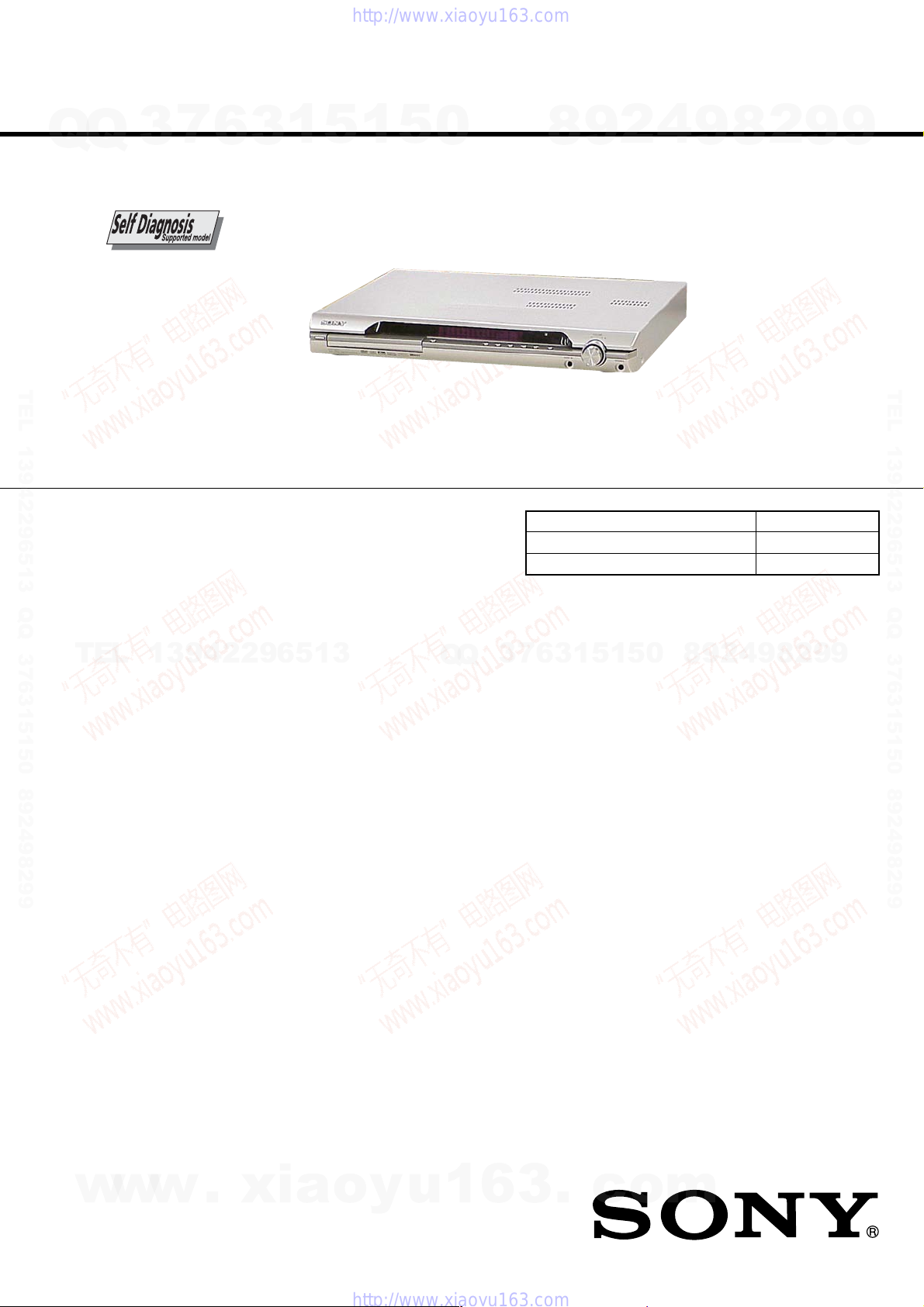
• HCD-DZ520K is the amplifier, D VD/CD
and tuner section in DAV-DZ520K.
• HCD-DZ620K is the amplifier, D VD/CD
and tuner section in DAV-DZ620K.
This system incorporates with Dolby*1 Digital and Dolby Pro Logic (II)
adaptive matrix surround decoder and the DTS*2 Digital Surround
System.
*1 Manufactured under license from Dolby Laboratories.
“Dolby,” “Pro Logic,” and the double-D symbol are trademarks of
Dolby Laboratories.
*2 Manufactured under license from Digital Theater Systems, Inc.
“DTS” and “DTS Digital Surround” are trademarks of Digital
Theater Systems, Inc.
TEL
13942296513
Photo : HCD-DZ520K
7
3
Q
Q
SPECIFICATIONS
8
9
2
4
9
8
2
9
9
E Model
HCD-DZ520K
Russian Model
HCD-DZ520K/DZ620K
Model Name Using Similar Mechanism HCD-DZ110
Mechanism T ype CDM85-DVBU102
Optical Pick-up Name
5
1
5
1
3
6
0
8
9
2
4
KHM-310CAA
9
2
8
9
9
TEL 13942296513 QQ 376315150 892498299
Amp
lifier section
DZ520K
Stereo mode (rated) 108 W + 108 W (3 ohms at
Surround mode (reference)
DZ620K
Stereo mode (rated) 108 W + 108 W (3 ohms at
Surround mode (reference)
1 kHz, 1 % THD)
RMS output power, 10 %
THD
Front: 142 W + 142 W
(with SS-TS53)
Center*: 142 W
(with SS-CT51)
Surround*: 142 W + 142
W
(with SS-TS51)
Subwoofer*: 140 W
(with SS-WS52)
1 kHz, 1 % THD)
RMS output power, 10 %
THD
Front: 143 W + 143 W
(with SS-TS53)
Center*: 143 W
(with SS-CT51)
Surround*: 143 W + 143
W
(with SS-TS53)
Subwoofer*: 285 W
(with SS-WS52B)
*Depending on the sound field settings and the source,
there may be no sound output.
Inputs (Analog)
TV/VCR (AUDIO IN/VIDEO IN)
Sensitivity: 450/250 mV
AUDIO IN/MIC 1/MIC
Sensitivity: AUDIO IN
250/125 mV/MIC 1 1 mv
MIC 2 Sensitivity: 1 mV
DVD system
Laser Semiconductor laser
(DVD: λ = 650 nm)
(CD: λ = 790 nm)
Emission duration:
continuous
Signal format system
Russian models: PAL
Other models: NTSC/PAL
Tuner section
System PLL quartz-locked digital
synthesizer system
FM tuner section
Tuning range 87.5-108.0 MHz (50 kHz
step)
Antenna (aerial) FM wire antenna (aerial)
Antenna (aerial) terminals 75 ohms, unbalanced
Intermediate frequency 10.7 MHz
AM tuner section
Tuning range
Middle Eastern and Russian models:
531-1,602 kHz (with the
interval set at 9 kHz)
Asian models: 531-1,602 kHz (with the
interval set at 9 kHz)
530-1,710 kHz (with the
interval set at 10 kHz)
Antenna (aerial) AM loop antenna (aerial)
Intermediate frequency 450 kHz
— Continued on next page —
DVD RECEIVER
w
w
9-887-197-01
2006D1678-1
© 2006.04
w
.
xia
Sony Corporation
Home Audio Division
Published by Sony Techno Create Corporation
o
y
u
1
6
3
.
c
o
m
SECTION 4
TEST MODE
HCD-DZ520K/DZ620K
7
Q
Q
TEL 13942296513 QQ 376315150 892498299
TEL
w
3
Note 1: Regarding the notification symbol “R”
Note 2: Incorrect operations may be performed if the test mode is
1. Cold Reset
• The cold reset clears all data including preset data stored in
the RAM to initial conditions. Execute this mode when
returning the set to the customers.
Procedure:
1. Press the ?/1 button to turn the power on.
2. Press three buttons x , A and ?/1 simultaneously.
3. When this button is operated, display as “COLD RESET” for
a while and all of the settings are reset.
2. Panel Test Mode
•This mode is used to check the software version, FL, LED
and KEY.
2-1. Display Test Mode
Procedure:
1. Press the ?/1 button to turn the power on.
2. Press three buttons X , . and A simultaneously.
3. When the display test mode is activated, all se gments and LEDs
13942296513
are turned on.
4. T o exit from this mode, press three b uttons X , . and A
simultaneously.
2-2. V ersion T est Mode
Procedure:
1. When the panal test mode is activated, press the . button
and the message “DSX2KF” (DZ520K), “DSX2KF+ ”
(DZ620K) are displayed, the version test mode is activated.
2. Whenever press the . button, the version is displayed in
order of CE2, MC, SYS, UI, DVD, ST, TA, DSP and TM.
3. Press the > button and the date of the software production
is displayed.
4. Press the > button again and the version is displayed.
5. T o exit from this mode, press three b uttons X , . and A
simultaneously.
2-3. Key Test Mode
Procedure:
1. When the panel test mode is activated, press the H button,
to select the key test mode.
2. T o enter the KEY test mode, the fluorecent indicator displays
“K0 V0”. Each time a button is pressed, “KEY” value
increases. However, once a button is pressed, it is no longer
taken into account. When all keys are pressed correctly, “K8
V0” is displayed.
3. When the V OLUME control is turned in the direction of (+),
“V0” is changed to “V1”, then ... “V9”.
When the V OLUME control is turned in the direction of (–),
“V0” is changed to “V9”, then ... “V1”.
4. T o exit from this mode, press three b uttons X , . and A
simultaneously.
w
w
6
Because the number of the operating buttons of this product
are limited, some operations require use of the operating
buttons of the remote commander, When a specific operation
requires use of the operating buttons of the remote
commander, “R” is added to the specific operating procedure
in this manual. Example MENU/NO “R” The MENU/NO
button of remote commander.
not entered properly.
In this case, press the ?/1 button to turn the po wer of f, and
retry to enter the test mode.
.
1
3
xia
5
o
1
y
5
u
0
Q
Q
1
3. Disc Tray Lock
The disc tray lock function for the antitheft of an demonstration
disc in the store is equipped.
Setting Procedure :
1. Press the ?/1 button to turn the set on.
2. Press the FUNCTION button to set DVD function.
3. Insert a disc.
4. Press the x button and the A button simultaneously for five
5. The message “LOCKED” is displayed and the tray is locked.
Releasing Procedure :
1. Press the x button and the A button simultaneously for five
2. The message “UNLOCKED” is displayed and the tray is
Note: When “LOCKED” is displayed, the slot lock is not released by
4. DVD Ship Mode
• Use this mode when returning the set to the customer after
Procedure:
1. Press the ?/1 button to turn the set on.
2. Press the FUNCTION button to set the function “DVD”.
3.
4. After a message “MECHA LOCK” is displayed on the
5. To exit from this mode, press the ?/1 button to turn the set on.
5. AM Step Change
•A step of AM channels can be changed over between 9 kHz
7
3
Procedure:
1. Press the ?/1 button to turn the set ON.
2. Select the function “TUNER”, and press FUNCTION button
3. Press the ?/1 button to turn the set OFF.
4. Press two buttons > and ?/1 simultaneously, and the
6. V olume Test Mode
Procedure:
1. Press the ?/1 button to turn the power on.
2. Press three buttons . , H and > simultaneously.
3. The message “VOLUME MAX” is displayed, when the
4. To exit from this mode, press the ?/1 button to turn the set of f.
7. Product Out
This mode moves the optical pick-up to the position durable to
vibration and clears all data including preset data stored in the RAM
to initial conditions. Use this mode when returning the set to the
customer after repair.
Procedure:
1. Press the ?/1 button to turn the power on.
2. Press the FUNCTION button to set the function “DVD”.
3.
4. After the “ST ANDBY” blinking display finishes, the message
6
3
4
2
9
8
seconds.
seconds. again.
unlocked.
turning power on/off with the ?/1 button.
repair.
Remove all discs, press two buttons x
neously.
fluorescent indicator tube, pull out the AC plug.
0
5
1
5
1
3
6
and 10 kHz.
to select the BAND “AM”.
display of fluorescent indicator tube changes to “AM 9 k
STEP” or “AM 10 k STEP”, and thus the channel step is
changed over.
VOLUME control is turned in the dirction of (+).
The message “VOLUME MIN” is displayed, when the
VOLUME control is turned in the dirction of (–).
Remove all discs, and then
?/1 simultaneously.
.
c
“MECHA LOCK” is displayed on the fluorescent indicator
tube disconnect the A C po wer plug, then the ship mode is set.
o
9
2
9
8
press three buttons > , A and
m
2
8
,
and . simulta-
8
9
4
9
2
9
9
9
TEL 13942296513 QQ 376315150 892498299
19
HCD-DZ520K/DZ620K
7
Q
Q
DVD SECTION
[TEST DISC LIST]
Be sure to use the DVD disc that matches the signal standards of
your region.
• CD YEDS-18 (Part No.: 3-702-101-01)
• DVD SL (Single Layer)
NTSC : HLX-503 (Part No.: J-6090-069-A)
PAL : HLX-506 (Part No.: J-6090-077-A)
• DVD DL (Dual Layer)
NTSC : HLX-501 (Part No.: J-6090-071-A)
TEL 13942296513 QQ 376315150 892498299
PAL : HLX-507 (Part No.: J-6090-078-A)
8-1. GENERAL DESCRIPTION
The Mirror Time and IOP measurement allows you to make
diagnosis and adjustment simply by using the remote commander
and monitor TV. The instructions, diagnosis results, etc. are given
on the on-screen display (OSD).
Be sure to execute the Mirror Time and IOP measurement when a
BU (Base Unit) is replaced.
8-2. HOW TO ENTER TEST MODE
While pressing the
VOLUME + with the DVD player in power on.
The Test Mode starts, then the menu shown below will be
displayed on the TV screen.
TEL
* During the TEST mode is running, the model name “DSX2KF”
is displayed for DZ520K in the “Remocon Diagnosis Menu”.
The model name “DSX2KF+” is displayed for DZ620K.
The menu above is the Remocon Diagnosis Menu screen which
consists of six main function. At the bottom of the menu screen,
the model name and IF-con version. To enter Mirror Time
Adjustment menu, press button 2 “R” on the remote commander
to enter Drive Manual Operation menu. To exit from the T est Mode,
press the power button on the remote commander.
8-3. DRIVE MANUAL OPERATION
The Drive Manual Operation menu consists of five main
function. By pressing 2 “R” button on the remote commander in
the Remocon Diagnosis Menu, the screen will appear as below.
1. Servo Control
2. Track/Layer Jump
3. Manual Adjustment
w
4. Tray Aging Mode
5. MIRR time Adjust
0. Return to Top Menu
3
PATD-012 (Part No.: 4-225-203-01)
HLX-504 (Part No.: J-6090-088-A)
HLX-505 (Part No.: J-6090-089-A)
x and A buttons simultaneously, turn
13942296513
Remocon Diagnosis Menu
0. External Chip Check
1. Servo Parameter Check
2. Drive Manual Operation
3. Emergency History Check
4. Version Information
Model Name : DSX2KF_XX
IF-con : V
Syscon : Ver.
Drive Manual Operation
w
w
6
er. XX.XX (XXXX)
X.XXX
.
1
3
xia
5
o
1
y
5
u
8-4. MIRROR TIME ADJUSTMENT
0
To enter Mirror Time Adjustment, press 5 “R” button on the remote
commander. The screen will appear as below.
1. CD MIRR time Check:
2. DVD MIRR time Check:
3. Threshold:
4. Save to EEPROM:
5. Default set MIRR time:
[Open] Tray open [Close] Tray close
[0] Return to previous menu
There are five main commands in the Mirr time Adjust menu as
shown in the figure above. The functions of each command are
described in the following page.
1. CD MIRR time Check
This command checks the Mirror time value for CD disc.
2. DVD MIRR time Check
This command checks the Mirror time value for DVD disc.
3. Threshold
This command displays the threshold value between CD and DVD
mirror time.
4. Save to EEPROM
This command saves an adjusted mirror time value to the EEPR OM.
7
3
Q
Q
5. Default set MIRR time
This command will set CD and DVD mirror time to firmware def ault
value.
[Open] / [Close]
Pressing the A button controls the tray for disc change
during mirror time adjustment.
[0] Return to previous menu
Press the 0 “R” button to return to previous menu.
8-4-1. EXECUTING MIRROR TIME ADJUSTMENT
In order to execute mirror time adjustment, the following standard
procedures must be followed.
(1) In power on, while pressing the x and A buttons
simultaneously, turn VOLUME + .
(2) Select “2. Drive Manual Operation”.
0. External Chip Check
1. Servo Parameter Check
2. Drive Manual Operation
3. Emergency History Check
4. Version information
Model Name : DSX2KF_XX
IF-con : Ver. XX.XX (XXXX)
Syscon : Ver. X.XXX
1
6
3
2
9
8
MIRR time Adjust Menu
0
5
1
5
1
3
6
Remocon Diagnosis Menu
.
c
o
4
8
m
9
9
8
2
4
2
9
8
9
2
9
9
TEL 13942296513 QQ 376315150 892498299
9
20
HCD-DZ520K/DZ620K
Q
TEL 13942296513 QQ 376315150 892498299
(3) Select “5. MIRR time Adjust”.
Q
(4) Select “5. Default set MIRR time”.
(5) Select “3. Threshold”.
(6) Confirm the number. If it is 7D, go to next step. If it is any
other value, return to step 4.
7
3
1. Servo Control
2. Track/Layer Jump
3. Manual Adjustment
4. Mecha test mode
5. MIRR time Adjust
0. Return to Top Menu
1. CD MIRR time Check:
2. DVD MIRR time Check:
3. Threshold:
4. Save to EEPROM:
5. Default set MIRR time:
[Open] Tray open [Close] Tray close
[0] Return to previous menu
6
Drive Manual Operation
MIRR time Adjust Menu
MIRR time Adjust Menu
3
1
5
1
5
0
(14) Confirm the same values are displayed. If it is not same,
return to step 7.
(15) Push the A button to eject tray.
(16) Take out HLX-504 and insert Test Disc YEDS-18 into
tray.
(17) Push the A button to close tray.
(18) Push “1. CD MIRR time check”.
(19) Wait for HEX number to display.
(20) Confirm the number, if YY is 5A – E8, proceed with next
step. If no, return to 15.
4
2
9
8
MIRR time Adjust Menu
1. CD MIRR time Check:
2. DVD MIRR time Check: XX XX
3. Threshold:
4. Save to EEPROM:
5. Default set MIRR time:
[Open] Tray open [close] Tray close
[0] Return to previous menu
MIRR time Adjust Menu
9
8
2
9
9
TEL 13942296513 QQ 376315150 892498299
1. CD MIRR time Check:
2. DVD MIRR time Check:
TEL
3. Threshold: 7D
13942296513
4. Save to EEPROM:
5. Default set MIRR time:
[Open] Tray open [Close] Tray close
[0] Return to previous menu
(7) Push the A button to eject tray.
(8) Insert Test Disc HLX-504 into tray.
(9) Push the A button to close tray.
(10) Push “2. DVD MIRR time Check”.
(11) Wait for HEX number to display.
(12) Confirm the number, if XX is 28 – 70, proceed with next
step. If no, return to 8.
MIRR time Adjust Menu
1. CD MIRR time Check:
2. DVD MIRR time Check: XX XX
3. Thereshold:
4. Save to EEPROM:
5. Default set MIRR time:
[Open] tray open [close] Tray close
[0] Return to previous menu
Q
Q
1. CD MIRR time Check: YY YY
2. DVD MIRR time Check: XX XX
3
4. Save to EEPROM:
5. Default set MIRR time:
[Open] Tray open [close] Tray close
[0] Return to previous menu
(21) Push “4. Save to EEPROM”.
(22) Confirm the same values are displayed. If it is not the
same, return to step 15.
1. CD MIRR time check: YY YY
2. DVD MIRR time check: XX XX
3. Threshold:
4. Save to EEPROM:
5. Default set MIRR time:
[Open] Tray open [close] Tray close
[0] Return to previous menu
(23) Push the A button to eject tray.
(24) Remove Test Disc YEDS-18 from tray.
(25) Push the A button to close tray.
(26) Press the 0 “R” button to the Drive Manual Operation menu.
3. Threshold:
5
1
3
6
7
0
5
1
MIRR time Adjust Menu
8
9
2
4
9
8
2
9
9
(13) Push “4. Save to EEPROM”.
w
w
w
.
xia
o
y
u
1
6
3
(27) Press the 0 “R” button to return to the Remocon Diagnosis
Menu.
(28) Press the ?/1 button to switch OFF set.
.
c
o
m
21
HCD-DZ520K/DZ620K
8-5. EXECUTING IOP MEASUREMENT
Q
Q
In order to execute mirror time adjustment, the following standard
procedures must be followed.
(1) In standby mode, while pressing the x and A buttons
simultaneously, turn VOLUME + .
0. External Chip Check
1. Servo Parameter Check
2. Drive Manual Operation
3. Emergency History Check
4. Version information
TEL 13942296513 QQ 376315150 892498299
Model Name : DSX2KF_XX
IF-con : Ver. XX.XX (XXXX)
Syscon : Ver. X.XXX
(2) Select “2. Drive Manual Operation” by pressing the 2 “R”
button on the remote commander. The screen will appear as
below.
1. Servo Control
2. Track/Layer Jump
3. Manual Adjustment
4. Tray Aging Mode
5. MIRR time adjust
0. Return to top Menu
7
3
Remocon Diagnosis Menu
Drive Manual Operation
6
3
1
5
1
5
(5) Wait until a hexadecimal number appear.
0
1. Track Balance Adjust:
2. Track Gain Adjust:
3. Focus Balance Adjust:
4. Focus Gain Adjust:
5. Eq Boost Adjust:
6. Iop. 5B:
7. TRV. Level:
8. S curve(FE) Level:
9. RFL(PI) Level:
0. MIRR Time:
Change Value
[0] Return to previous menu
(6) Convert each data from hexadecimal to decimal using
conversion table.
(7) Substract between these two values.
(8) If the remainder is smaller than 93 (decimal), then it is
OK. However if the value is higher than 93, then the BU
is defective and need to be change.
(9) Press the RETURN “R” button to return back to previous
menu.
(10) Press the 0 “R” button to return to Top Menu and power
OFF the DVD Player.
8
2
9
Manual Adjust
4
9
8
2
9
9
TEL 13942296513 QQ 376315150 892498299
TEL
(3) Select “3. Manual Adjustment” by pressing the 3 “R” b utton
on the remote commander. The screen will appear as below.
1. Track Balance Adjust:
2. Track Gain Adjust:
3. Focus Balance Adjust:
4. Focus Gain Adjust:
5. Eq boost Adjust:
6. Iop:
7. TRV. Level:
8. S curve(FE) Level:
9. RFL(PI) Level:
0. MIRR Time:
o O Change Value
[RETURN] Return to previous menu
(4) Select Iop by pressing the 6 “R” button on the remote
commander.
13942296513
Manual Adjust
Q
Q
3
7
6
3
1
5
1
5
0
8
9
2
4
9
8
2
9
9
22
w
w
w
.
xia
o
y
u
1
6
3
.
c
o
m
)
SECTION 5
ELECTRICAL ADJUSTMENT
HCD-DZ520K/DZ620K
7
Q
Q
TEL 13942296513 QQ 376315150 892498299
TEL
3
DVD SECTION
When the base unit is replaced, perform the adjustment and the
measurement as shown below in this order.
1) MIRROR TIME ADJUSTMENT (See page 20)
2) EXECUTING IOP MEASUREMENT (See page 22)
[TEST DISC LIST]
Be sure to use the DVD disc that matches the signal standards of
your region.
• CD YEDS-18 (Part No.: 3-702-101-01)
• DVD SL (Single Layer)
NTSC : HLX-503 (Part No.: J-6090-069-A)
PAL : HLX-506 (Part No.: J-6090-077-A)
• DVD DL (Dual Layer)
NTSC : HLX-501 (Part No.: J-6090-071-A)
PAL : HLX-507 (Part No.: J-6090-078-A)
[RF Level Check]
Connection:
CN1105 pin 6 (RFMON)
CN1105 pin 3 (GND)
13942296513
6
PATD-012 (Part No.: 4-225-203-01)
HLX-504 (Part No.: J-6090-088-A)
HLX-505 (Part No.: J-6090-089-A)
MAIN board
3
1
5
oscilloscope
1
+
–
5
0
Q
Q
Checking Location: MAIN board (Side A)
MAIN BOARD
7
3
4
2
9
8
(SIDE A)
CN1105 Pin 3 (GND)
CN1105 Pin 6 (RFMON)
0
5
1
5
1
3
6
9
8
CN1105
2
9
8
3
6
4
2
IC501
IC1103
9
8
9
2
9
9
TEL 13942296513 QQ 376315150 892498299
9
Procedure:
1. Connect an oscilloscope to CN1105 pin 6 (RFMON) and
CN1105 pin 3 (GND) on the MAIN board.
2. Turn the power on.
3. Insert the CD test disc (refer to the TEST DISC LIST), and
press the H button to play the disc back.
4. Confirm that oscilloscope waveform is clear and check RF
signal level is correct or not.
Note: A clear RF signal waveform means that the shape “◊” can be
clearly distinguished at the center of the waveform.
5. Eject the CD disc, and insert the DVD SL test disc (refer to
the TEST DISC LIST), and press the H button to play the
disc back.
RF signal waveform
VOLT/DIV: 200 mV
TIME/DIV: 500 ns
level: 0.57 to 1.1 Vp-p (CD)
0.58 to 1.23 Vp-p (DVD
w
w
w
.
xia
o
y
u
1
6
3
.
c
o
m
23
HCD-DZ520K/DZ620K
C
B
These are omitted.
E
Q
SECTION 6
DIAGRAMS
7
Q
Q
THIS NOTE IS COMMON FOR PRINTED WIRING BOARDS AND SCHEMATIC DIAGRAMS.
(In addition to this, the necessary note is printed in each block.)
For Schematic Diagrams.
Note:
• All capacitors are in µF unless otherwise noted. (p: pF)
50 WV or less are not indicated except f or electrolytics and
tantalums.
• All resistors are in Ω and 1/
specified.
• f : internal component.
• C : panel designation.
Note: The components identified by mark 0 or dotted
TEL 13942296513 QQ 376315150 892498299
✩ New part of EEP ROM (IC1103) on the MAIN board
cannot be used. Therefore, if the mounted MAIN board
(A-1144-746-A, etc.) is replaced, exchange new EEP
ROM (IC1103) with that used before the replacement.
• A : B+ Line.
•Voltages and wavef orms are dc with respect to ground under no-signal (detuned) conditions.
•Voltages and waveforms are dc with respect to ground in
service mode.
•Waveforms are taken with a oscilloscope.
Voltage v ariations ma y be noted due to normal production
tolerances.
no mark : DVD STOP
* : Impossible to measure
•Voltages are taken with VOM (Input impedance 10 MΩ).
• Circled numbers refer to waveforms.
• Signal path.
F : AUDIO
TEL
J : CD PLAY
c : DVD PLAY
I : SACD PLAY
d : TUNER
L : VIDEO
E : Y
a : CHROMA
r : COMPONENT VIDEO
f : AUDIO IN
•Abbreviation
E3 : 240V AC area in E model
RU : Russian model
SP : Singapore model
3
line with mark 0 are critical for safety.
Replace only with part number specified.
13942296513
6
4
W or less unless otherwise
3
1
5
1
5
0
For Printed Wiring Boards.
Note:
• X : parts extracted from the component side.
• a : Through hole.
• : Pattern from the side which enables seeing.
(The other layers' patterns are not indicated.)
Caution:
Parts face side: Parts on the parts face side seen from
(SIDE A) the parts face are indicated.
Pattern face side: Parts on the pattern face side seen from
(SIDE B) the pattern face are indicated.
• Indication of transistor.
CEB
These are omitted
6
7
3
Q
Q
8
3
9
1
5
2
1
5
4
0
9
8
9
8
2
4
2
9
8
9
2
9
9
TEL 13942296513 QQ 376315150 892498299
9
w
w
w
24
.
xia
o
y
u
1
6
3
.
c
o
m
HCD-DZ520K/DZ620K
• Circuit Boards Location
Q
TEL 13942296513 QQ 376315150 892498299
Q
SW board
3
MS-203 board
7
TUNER UNIT
6
3
1
IO-S TERMINAL board
5
SPEAKER board
HEATSINK B board
1
MAIN board
HEATSINK A board
5
0
•Waveforms
– MAIN Board –
1 IC1101 6 (DVDRFIP)
200 mV/DIV, 100 ns/DIV
2 IC1101 <xx. (XTALI)
1 V/DIV, 10 ns/DIV
3
IC1101 <z., (YUV3)
8
37 ns
9
900 mVp-p
1.7 Vp-p
1.5 Vp-p
– IO-S TERMINAL Board –
2
4
6
IC201 wh (COUT)
H
1 V/DIV, 20 µs/DIV
7
IC201 wa (YOUT)
1 V/DIV, 20 µs/DIV
8
IC201 w; (CYOUT)
9
H
8
2.0 Vp-p
2.2 Vp-p
2.2 Vp-p
2
9
IC201 qk (CbOUT)
500 mV/DIV, 20 µs/DIV
0
IC201 qh (CrOUT)
500 mV/DIV, 20 µs/DIV
9
H
H
9
1.6 Vp-p
TEL 13942296513 QQ 376315150 892498299
1.6 Vp-p
T
E
L
1
3
9
4
2
DDCON board
2
FL board
9
6
JACK board
POWER board
5
1
3
Q
Q
H
6
7
3
500 mV/DIV, 20 µs/DIV
4 IC501 qg (XIN)
200 ns
1 V/DIV, 100 ns/DIV
5
IC3010 rk (XFSOIN)
20.3 ns
1 V/DIV, 10 ns/DIV
3
1
5
2.7 Vp-p
5.5 Vp-p
1
5
0
1 V/DIV, 20 µs/DIV
8
9
H
9
9
2
8
9
4
2
w
HCD-DZ520K/DZ620K
w
w
.
x
i
a
o
y
u
1
6
3
2525
.
c
o
m
HCD-DZ520K/DZ620K
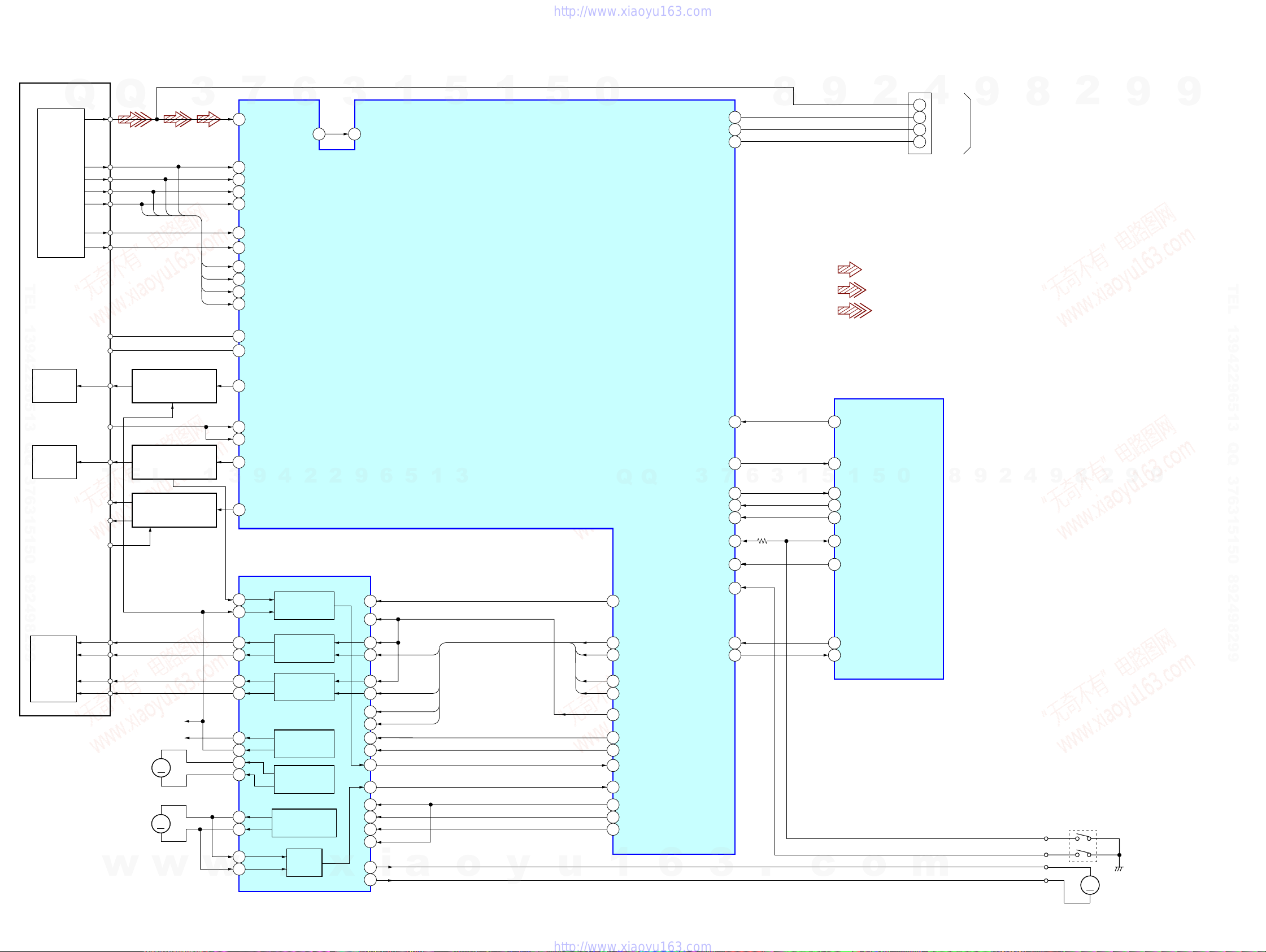
6-1. BLOCK DIAGRAM – RF SECTION –
Q
DETECTOR
TEL 13942296513 QQ 376315150 892498299
OPTICAL PICK-UP
BLOCK
(KHM-310CAA)
LASER
DIODE
(FOR CD)
RF
VC
LIMIT
CD LD
A
B
C
D
F
E
Q
D
AUTOMATIC POWER
CONTROL (FOR CD)
C
Q1102 (1/2)
3
B
A
7
DVDRFIP
6
DVDA
2
DVDB
3
DVDC
4
DVDD
5
19
TPI
18
8
9
10
11
29
176
23
TNI
NA
NB
MD
MC
V2O
LI M SW
LD01
A
B
D
C
6
OSP
3
252 253
OSN
1
5
IC1101 (1/3)
CD/DVD RF AMP,
FOCUS/TRACKING ERROR AMP
DVD SYSTEM PROCESSOR
DIGITAL SERVO PROCESSOR
1
5
0
V2REFO
RXD
TXD
28
106
107
8
9
• Signal Path
CONTROLLER
2
: CD PLAY
: DVD PLAY
: SACD PLAY
IC501 (1/4)
SYSTEM
CN1105
4
6
5
2
1
RFMON
V2REFO
RXD
TXD
9
TO DIAG JIG
8
2
9
9
TEL 13942296513 QQ 376315150 892498299
LASER
DIODE
(FOR DVD)
2AXIS
DEVICE
FOCUS/
TRACKING
COIL
PD
DVD LD
T
E
VR650
VR780
MSW
FCS+
FCS–
TRK+
TRK–
(SLED MOTOR)
(SPINDLE MOTOR)
w
Q1102 (2/2)
AUTOMATIC POWER
CONTROL (FOR DVD)
L
Q1101, Q1103
VOLUME CONTROL
+3.6V
+2.5V
MM
MM
w
1
SL–
SL+
SP+
SP–
w
20
MD12
MD11
21
LD02
22
3
9
4
2
2
MSW
50
FOCUS/TRACKING COIL DRIVER,
SPINDLE, SLED MOTOR DRIVER
IOP
42
41
36 48
37 1
35 3
34 4
32
31
30
29
27
28
47
46
IC1201
BUFFER
FOCUS COIL
DRIVE
TRACKING COIL
DRIVE
SLED MOTOR
DRIVE
SLED MOTOR
DRIVE
SPINDLE MOTOR
DRIVE
BUFFER
.
x
9
6
.
SYSRST
SCO
3
SCD
SID
1
5
c
43
MTK_RST
33
DVD_SCO
1
32
DVD_SOD
31
DVD_SID
37
DVD_XIFCS
27
CDM_OPEN_SW
34
DVD_XIFBUSY
35
MIC_DET
36
KARAOKE_MODE
o
5
0
m
8
9
4
2
OCSW1
OCSW/CKSW
LDM+
LDM-
2
8
9
S001
(CHUCK/TRAY DETECT)
(LOADING MOTOR)
MM
9
9
110
PRST
99
IFCK
6
5
1
3
15
43
10
13
16
17
40
45
19
20
22
21
25
22
i
24
VREFO
FOO
TRO
FMO
DMO
a
o
y
FMO
FOO
DMO
TRO
u
Q
39
TROPENPWN
38
FMO
42
FOO
37
DND
41
TRO
V REFO
30
174
FWD
178
REV
40
IOPMON
47
SPFG
211
MUTE123
210
MUTE
170
TSDM
1
Q
6
3
IFSDO
IFSDI
XIFCS
OCSW
IFBSY
CKSW
MIC
KRMOD
3
7
98
101
100
177
105
179
205
207
HCD-DZ520K/DZ620K
2626

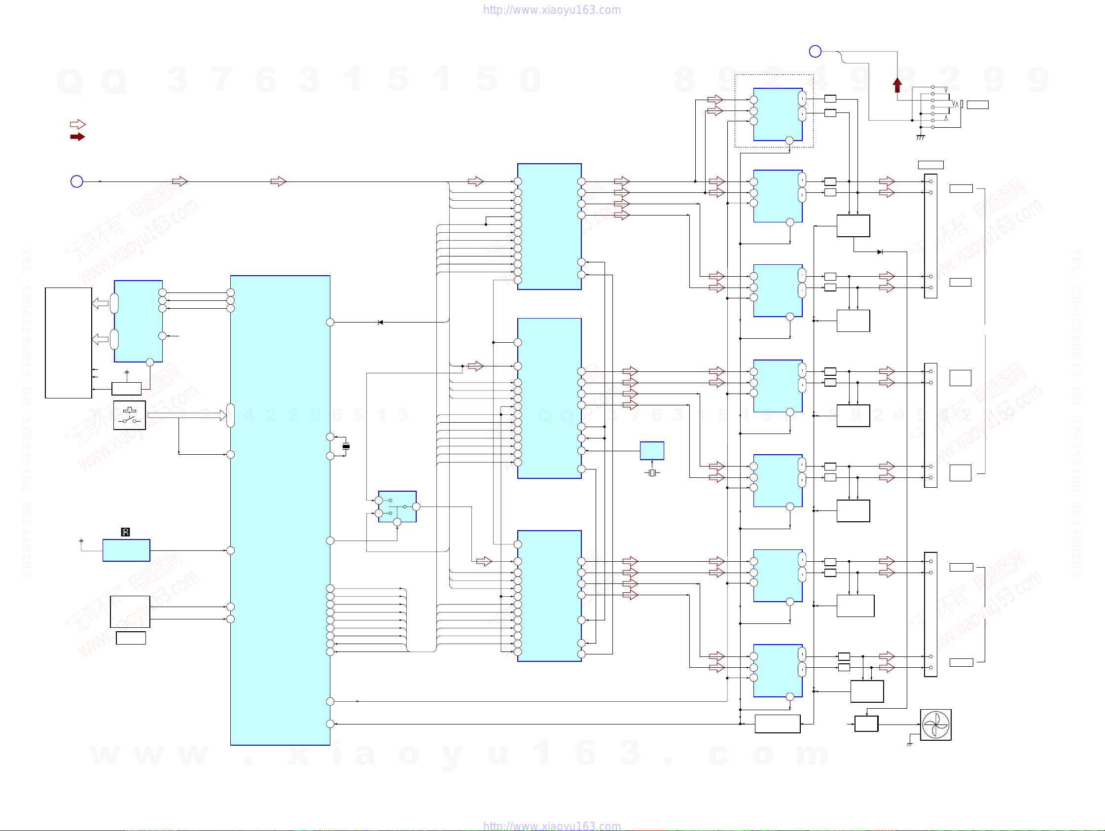
6-2. BLOCK DIAGRAM – AMP SECTION –
HCD-DZ520K/DZ620K
Q
AUDIO IN/MIC 1/
A.CAL MIC
Q
J401
3
Q470-473,476
MO/ST DETECT
TEL 13942296513 QQ 376315150 892498299
D433 D470
J203
TV/VCR
L
R
7
6
5
3
2
AUDIO
SECTION
(Page 28)
IC401
AMP
–
+
+
–
C
6
7
1
+9V
GAIN CONT
MIC2
Q474,475
3
IC402
AMP
5
+
–
6
3
+
–
2
1
7
1
PLUG DET2
Q477-478
PLUG DET
GAIN CONT ACAL
DC CONT
MO/ST DET
PLUG DET1
5
Q300,310,320
MUTING
1
1
VIN2
VIN2
8
DATA
4
Q355
RDS DATA
IC371
BUFFER
VOUT1
VOUT2
CLK
5
RDS CLK
5
2
7
Q351
IC1101 (2/3)
2
SDATA0
SDATA1
SDATA2
ALRCK
ABCK
ACLK
9
217
218
219
213
214
215
9
AMP LRCKO
AMP BCKO
AMP MCKO
AMP D1
AMP D2
AMP D3
AUDIO
SECTION
A
(Page 28)
TEL 13942296513 QQ 376315150 892498299
LIN
RIN
4
9
IC2200
A/D CONVERTER
1
LIN
RIN
2
DOUT
LRCK
SCKI
8
12
10
11
BCK
15
DVD SYSTEM PROCESSOR
209
SPDATA
DWIDE
224
0
AUDIO INPUT SELECTOR
11
L
+5V
+
+
IC372
COMPARATOR
3
+
–
2
1
R
X3
15
X2
14
X1
X0
12
4
Y3
2
Y2
5
Y1
Y0
1
Q395
IC350
A
10B9
A SEL1
A SEL0
8
13
X
3
Y
Q396
9
2
3
+
1
–
2
5
+
7
–
6
IC360
AMP
T
E
TUNER
UNIT
L
L-CH
R-CH
1
3
RDS_DATA
RDS_CLK
TUNED
PLL CK
PLL DO
PLL CE
PLL DI
9
4
2
2
9
6
5
1
3
Q
Q
3
VIDEO
SECTION
(Page 29)
B
7
ACAL
6
GAIN CONT
MO/ST DET
PLUG DET1
RDS_DATA
RDS_CLK
TUNED
PLL CK
PLL DO
PLL CE
PLL DI
V_SEL0
V_SEL1
DVD_SEL
3
82
A-SEL0
A-SEL1
83
ACAL MIC LEVEL
91
1
MIC GAIN
26
DC CONT
28
MONO/ST DET
90
MIC/A CALSW
100
RDS_DATA
76
RDS_CLK
75
TUNED
69
ST_CLK
70
ST_DO
71
ST_CE
72
ST_DI
73
V_SEL0
71
V_SEL1
72
TVSEL/V_SEL3
81
IC501 (2/4)
SYSTEM CONTROL
5
1
5
0
8
9
2
4
9
8
2
• Signal Path
9
: AUDIO
: AUDIO IN
: TUNER
9
w
HCD-DZ520K/DZ620K
w
w
.
x
i
a
o
y
u
1
6
3
2727
.
c
o
m
HCD-DZ520K/DZ620K
6-3. BLOCK DIAGRAM – AUDIO SECTION –
Q
AMP
SECTION
(Page 27)
Q
• Signal Path
: AUDIO
: AUDIO IN
AMP_D1-D3
AMP_BCK0,LRCK0,MCK0
A
3
7
6
3
TEL 13942296513 QQ 376315150 892498299
IC501 (3/4)
SYSTEM CONTROLLER
4
2
KEY0 – KEY2
DIPCSFLAG
2
9
Xout
MST
DAMP SCDT
DAMP SHIFT
DAMP LAT1
DAMP LAT2
DAMP LAT3
DAMP INIT
DAMP SOFT MUTE
OVERFLOW1
OVERFLOW2
DRIVE RST
DRIVE OCP
19
6
13
Xin
15
68
1
2
47
48
49
50
51
44
45
42
43
FL801
FLUORESCENT
INDICATOR TUBE
(FUNCTION KEY)
E3.3V
F1
F2
G1
S801 – S808
T
IC802
FL DRIVER
14 – 29
SG1 – SG16
41 – 31
GR2 – GR12
+3.3V
Q802
FL DRIVER
E
L
IC801
REMOTE CONTROL
RECEIVER
S800
VOLUME
ENCODER
VOLUME
DIN
CLK
STB
42
GR1
3
9
24
21
25
97,95,94
74
4
10
11
FL DATA
FL CLK
FL CS/STB
KEY INT
SIRCS–IN
ENA
ENB
7
8
9
30
VFL
1
KEY0
1
5
X502
5MHz
5
D3071-D3073
1
SELECTER
2
1
SCDT
SHIFT
LAT1
LAT2
LAT3
SOFTMUTE
OVF2
RESET
DIAG
3
IC3003
6
AMP_D2
INIT
OVF
AMP_D0-D3
5
1
AMP_D3
MCK0
BCK0
LRCK0
OVF2
SCDT
SHIFT
LAT3
INIT
NSPMUTE
SOFTMUTE
AMP_D1
MCK0
BCK0
LRCK0
OVF
SCDT
SHIFT
LAT1
INIT
NSPMUTE
SOFTMUTE
MCK0
BCK0
LRCK0
SCDT
SHIFT
LAT2
INIT
NSPMUTE
SOFTMUTE
5
0
IC3030
S-MASTER PROCESSOR
31
DATA
36
XFSIIN
30
BCK
29
LRCK
25
FLAGL OVF
24
OVF FLAGR
21
SCDT
22
SCSHIFT
23
SCLATCH
27
INIT
18
NSPMUTE
19
SOFTMUTE
20
PGMUTE
IC3010
S-MASTER PROCESSOR
20
PGMUTE
31
DATA
36
XFSIIN
30
BCK
29
LRCK
25
FLAGL OVF
24
OVF FLAGR
Q
21
SCDT
22
23
27
18
19
20
31
36
30
29
25
21
22
23
27
18
19
24
FSOCKOUT
SCSHIFT
SCLATCH
INIT
NSPMUTE
SOFTMUTE
XFS0OUT
IC3020
S-MASTER PROCESSOR
PGMUTE
DATA
XFSIIN
BCK
LRCK
FLAGL OVF
SCDT
SCSHIFT
SCLATCH
INIT
NSPMUTE
SOFTMUTE
OVF FLAGR
XFS0OUT
OUTL1
OUTL2
OUTR1
OUTR2
FS0I
XFS0IN
OUTR1
OUTR2
OUTL1
OUTL2
Q
FS0I
XFS0IN
OUTR1
OUTR2
OUTL1
OUTL2
FS0I
XFS0IN
AMP
C
SECTION
(Page 27)
DZ620K
8
11
9
6
4
WF
WF
C
C
9
IC3500
S-MASTER DIGITAL AMP
2
PWMB
PWMA
RESET
PWMB
PWMA
RESET
IC3400
OUTA
OUTB
OUTB
OUTA
SD
4
SD
4
14
6
5
S-MASTER DIGITAL AMP
14
6
5
4
28
30
25
27
25
27
28
30
LPF
LPF
LPF
LPF
MIC2
PLUG DET2
9
Q3401,3402
DC
DETECT
8
SPEAKER
2
(+)
WOOFER
(–)
J402
MIC 2
9
9
TEL 13942296513 QQ 376315150 892498299
IC3300
38
48
7
FR
FR
FL
FL
6
IC3051
OSC
X450
49.152MHz
SR
SR
SL
SL
3
1
5
6
4
11
9
3
37
38
48
14
6
4
11
9
38
48
14
S-MASTER DIGITAL AMP
6
PWMA
14
PWMB
RESET
5
IC3100
S-MASTER DIGITAL AMP
14
PWMB
6
PWMA
RESET
5
5
1
IC3150
S-MASTER DIGITAL AMP
6
PWMA
14
PWMB
RESET
5
IC3200
S-MASTER DIGITAL AMP
14
PWMB
6
PWMA
RESET
5
IC3250
S-MASTER DIGITAL AMP
6
PWMBP
14
PWMAP
RESET
5
Q3551
PROTECT DETECT
OUTA
OUTB
OUTB
OUTA
0
OUTB
OUTA
OUTA
OUTB
OUTA
OUTB
28
LPF
30
25
LPF
27
SD
4
25
27
28
30
SD
4
28
30
25
27
SD
4
25
27
28
30
SD
4
28
30
25
27
SD
4
LPF
LPF
8
LPF
LPF
LPF
LPF
Q3301,3302
DETECT
Q3101,3102
DETECT
Q3151,3152
DETECT
Q3201,3202
DETECT
LPF
LPF
+12V
DC
DC
9
DC
DC
Q3251,3252
DC
DETECT
FAN
DRIVE
Q3000-3002
2
4
9
FAN
(+)
(–)
(+)
(–)
8
(+)
(–)
(+)
(–)
(+)
(–)
CENTER
FRONT
R
2
FRONT
L
SUR R
SUR L
TB301
9
TB302
9
w
HCD-DZ520K/DZ620K
w
w
.
x
i
a
o
y
u
1
6
2828
3
.
c
o
m
HCD-DZ520K/DZ620K
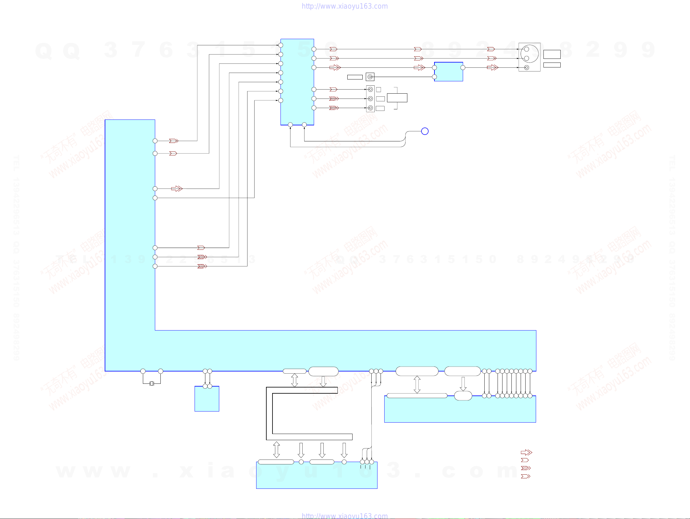
6-4. BLOCK DIAGRAM – VIDEO SECTION –
Q
Q
3
TEL 13942296513 QQ 376315150 892498299
7
YUV2
YUV1
YUV3
WIDE
196
194
198
49
6
3
1
WIDE
5
1
2
6
4
10
12
14
25
IC201
VIDEO AMP, 75Ω DRIVE
CIN
YIN
CVBSIN
CYIN
CBIN
CRIN
S1
5
CVBSOUT
3 13
COUT
YOUT
CYOUT
CbOUT
CrOUT
26
0
21
23
20
18
16
J203
VIDEO IN
P
PR/C
Y
B/CB
R
J203
COMPONENT
VIDEO OUT
V SEL0
V SEL1
8
B
2
CIN2CIN
6
YIN
VIDEO SELECTOR
AMP
SECTION
(Page 27)
9
IC202
2
C
4
Y
V
1
2
9
J201
S VIDEO
(DVD ONLY)
VIDEO
8
2
9
9
TEL 13942296513 QQ 376315150 892498299
T
E
L
1
3
9
228
YUV4
YUV5
YUV6
4
X1102
27MHz
SCL
102
6 5
SCL
IC1103
6
103
SDA
SDA
CY
CB
5
CR
1
3
IC1101(3/3)
DVD SYSTEM PROCESSOR
AD0 – AD7
81-84,86-88,91
HD0 – HD7 A0 – A21
DATA & ADDRESS BUS
HIGHA0-7
IOA0-7, IOA18-IOA21
A16, A17
53-61, 67-72, 74-76,
78, 89, 92, 93
Q
Q
IOCS
77
XRD
XROMCS
6
7
3
IOWA79IOUE
66
XWR
2,4,5,7,8,10,11,13,42,44,45,47,48,50,51,53
RD0 – RD15
125-123, 121, 120, 118,
117, 115, 135, 133-128, 126
RD0 – RD15
3
1
1
5
RA0 – RA11
146, 147, 149-151,
158-160, 162, 164-166
22-26,
29-35
RA0 – RA11
IC1104
64M SDRAM
0
5
RCLK
BA0
BA1
142
143
145 156 113 137 157
38
19
20
21
BS0
BS1
DRCLK
RCS
RCS
9
9
2
8
9
4
2
9
8
RWE
MRAS
CAS
MDQM0
MDQM1
RAS
CLE
139
17
15
39
37
CAS
DQM0
DQM1
DRCLE
138
140
16
18
RWE
200
202
2
2
203
229
9
EEPROM
w
HCD-DZ520K/DZ620K
w
w
.
x
i
a
DATA & ADDRESS BUS
HD0 – HD7
29,31,33,35,38,40,42,44 25-16, 9-1, 48
DQ0 – DQ7
o
y
A0
A0 – A19DQ15/A-1
IC1102
u
32M FLASH ROM
A1-A20
1
A21
XRD
XROMCS
XWR
2645
10
NC
28OE11
CE
6
WE
3
.
c
o
m
• Signal Path
: VIDEO
: Y
: COMPONENT VIDEO
: CHROMA
2929
HCD-DZ520K/DZ620K
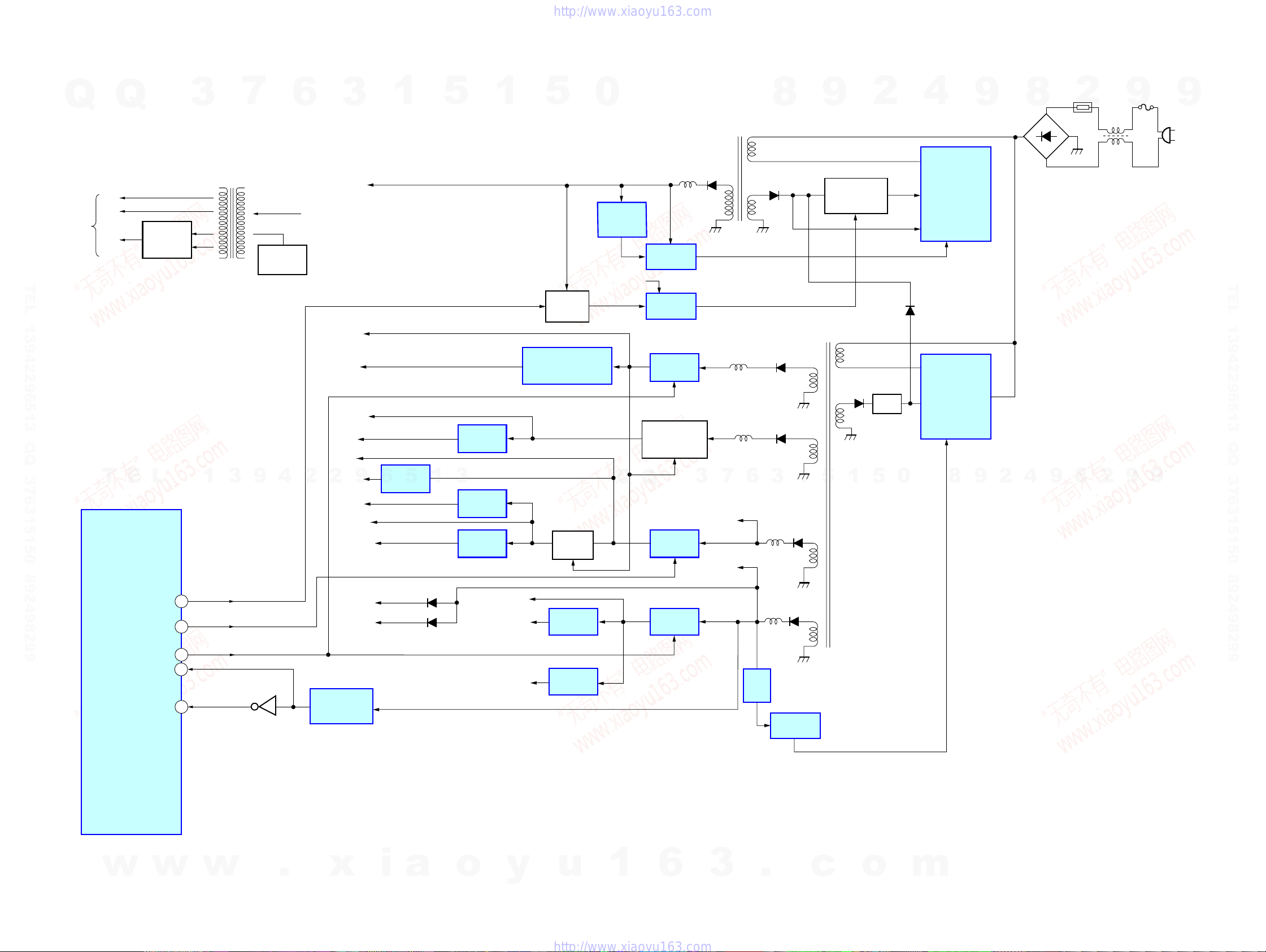
6-5. BLOCK DIAGRAM – POWER SECTION –
Q
TO FLUORESCENT
INDICATOR TUBE
TEL 13942296513 QQ 376315150 892498299
Q
F1
F2
VFL
D801,802
D804,805
3
RECT
7
T801
DC/DC
CONVERTER
OSC
Q801
6
+5V
3
+31.5V
A12V
1
5
1
5
Q943,947
VOLTAGE
DETECT
0
IC931
VOLTAGE
DETECT
E4V
PC901
PHOTO
COUPLER
PHOTO
COUPLER
T901
TRANSFORMER(MAIN)
D931
PC903
8
D905
9
T902
TRANSFORMER (SUB)
Q901
VOLTAGE
CONTROLLER
2
4
POWER
PROTECTION
D910
IC901
9
D901
8
POWER
Thermistor
2
LINE
FILTER
F901
9
9
AC IN
TEL 13942296513 QQ 376315150 892498299
T
E
IC501 (4/4)
SYSTEM CONTROLLER
L
6
D941
D944
3
D942
D943
IC951
VOLTAGE
DETECT
PC902
PHOTO
COUPLER
1
5
D922
1
Q921
5
REG
0
IC921
POWER
PROTECTION
8
9
2
4
9
8
2
9
9
+9V
SW+9V
A5V
+5V
1
3
9
4
2
40P CONT2
41P CONT3
39P CONT1
20AC_CUT
Q506
12RESET
+3.3V
2
+3.3V
SW +5V
RF +3.3V
BMP3.3V
IC511
RESET
9
E3.3V
IC502
6
+3.3V REG
5
1
D503
D505
IC516
+5V REG
3
IC1105
+3.3V REG
IC1107
+3.3V REG
SW+3.3V,+3.3V
+1.8V
+1.8V
IC300
+9V REG
Q
Q502
5V SW
IC1109
+1.8V REG
IC3050
+1.8V REG
IC941
+12V REG
Q945
MOTOR DRIVE
CONTROLLER
Q
IC942
D+5V REG
IC943
+3.3V REG
3
7
+6V
E 4V
w
HCD-DZ520K/DZ620K
w
w
.
x
i
a
o
y
u
1
3030
6
3
.
c
o
m
HCD-DZ520K/DZ620K
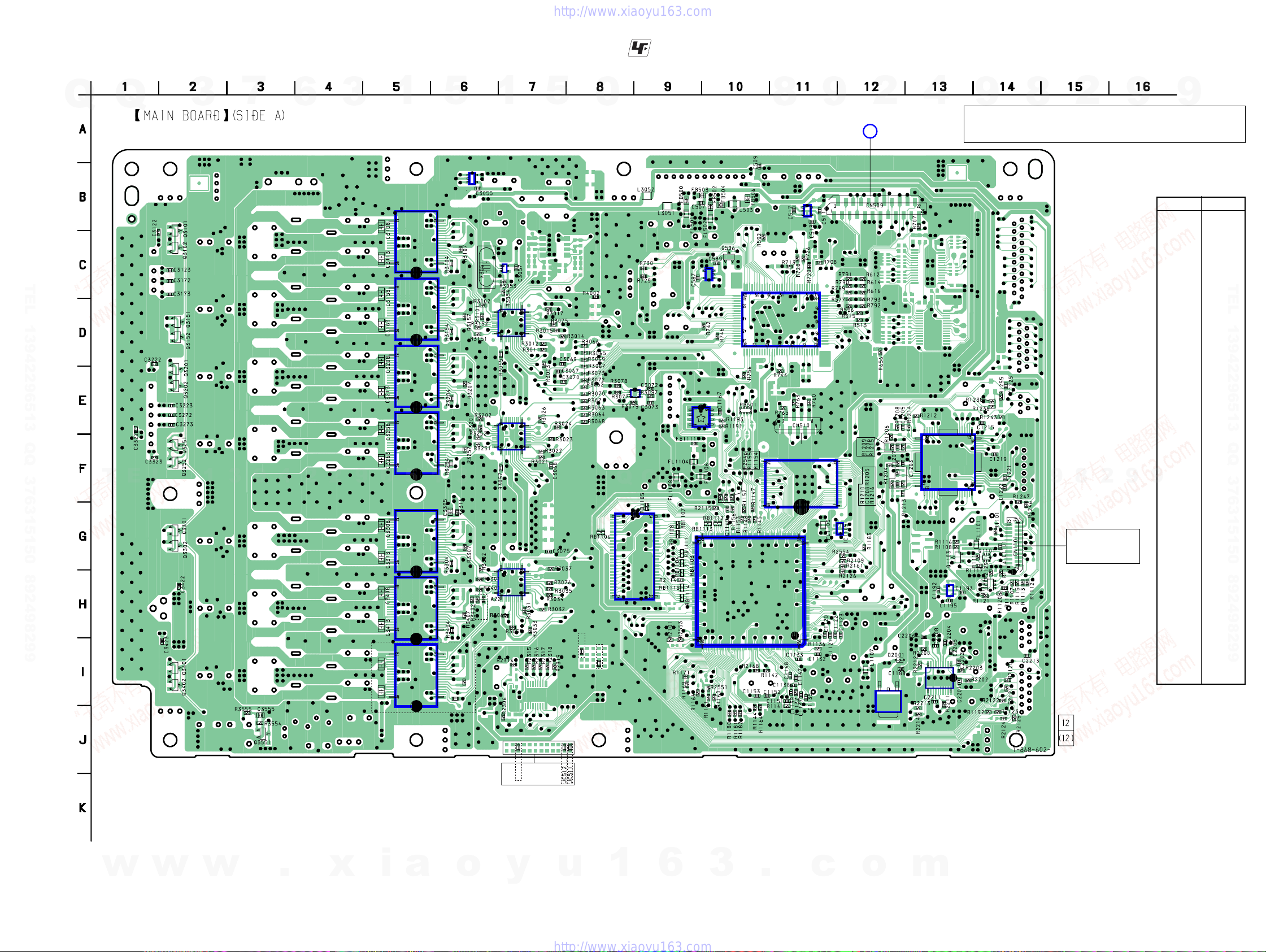
6-6. PRINTED WIRING BOARD – MAIN BOARD (SIDE A) –
3
7
9
4
6
2
2
3
9
Q
TEL 13942296513 QQ 376315150 892498299
T
Q
E
L
3
E
E
E
E
E
E
E
E
1
1
6
• See page 25 for Circuit Boards Location.
IC3100
IC3150
IC3200
IC3250
5
1
5
IC3050
3
5
1
34
IC3051
1
IC3010
IC3020
5
0
IC3003
Q
Q
:Uses unleaded solder.
E
4
3
IC511
1
5
IC1103
6
7
3
8
IC502
IC501
3
IC1102
9
5
1
4
3
for WRITER JIG
5
1
1
2
A
5
FL BOARD
CN801
(Page 46)
0
4
IC1201
8
2
8
4
9
✩ New part of EEP ROM (IC1103) on the MAIN board cannot be used.
Therefore, if the mounted MAIN board (A-1144-746-A, etc.) is replaced,
exchange new EEP ROM (IC1103) with that used before the replacement.
9
9
2
8
2
9
9
9
• Semiconductor
Location
Ref. No.
D2001 I-12
IC501 D-11
IC502 B-11
IC511 C-10
IC1101 H-10
IC1102 F-11
IC1103 E-9
IC1104 H-8
IC1105 G-12
IC1107 H-13
IC1109 J-12
IC1201 F-13
IC2200 I-13
IC3001 C-7
IC3003 E-8
IC3010 D-7
IC3020 E-7
IC3030 H-7
IC3050 B-6
IC3051 C-7
IC3100 C-5
IC3150 D-5
IC3200 E-5
IC3250 F-5
IC3300 G-5
9
IC3400 H-5
IC3500 I-5
Location
TEL 13942296513 QQ 376315150 892498299
IC1105
E
E
E
E
E
C3508
C3513
IC3300
IC3400
IC3500
DZ620K
R3504
R3507
R3052
DZ620K
R3051
IC3030
JC520
RU
IC1104
DZ520K
JC505
E3
SP
DZ620K
JC507
IC1101
3
IC1109
1
IC1107
IC2200
10
20
11
E
1
OPTICAL
PICK-UP BLOCK
(KHM-310CAA)
Q506 C-10
Q1101 G-14
Q1102 H-14
Q1103 G-13
Q3101 C-2
Q3102 C-2
Q3151 D-2
Q3152 D-2
Q3201 E-2
Q3202 E-2
Q3251 F-2
Q3252 F-2
Q3301 G-2
Q3302 G-2
Q3401 I-2
Q3402 I-2
Q3551 J-3
w
HCD-DZ520K/DZ620K
w
w
.
x
i
a
o
y
u
1
6
3
3131
.
c
o
m
HCD-DZ520K/DZ620K
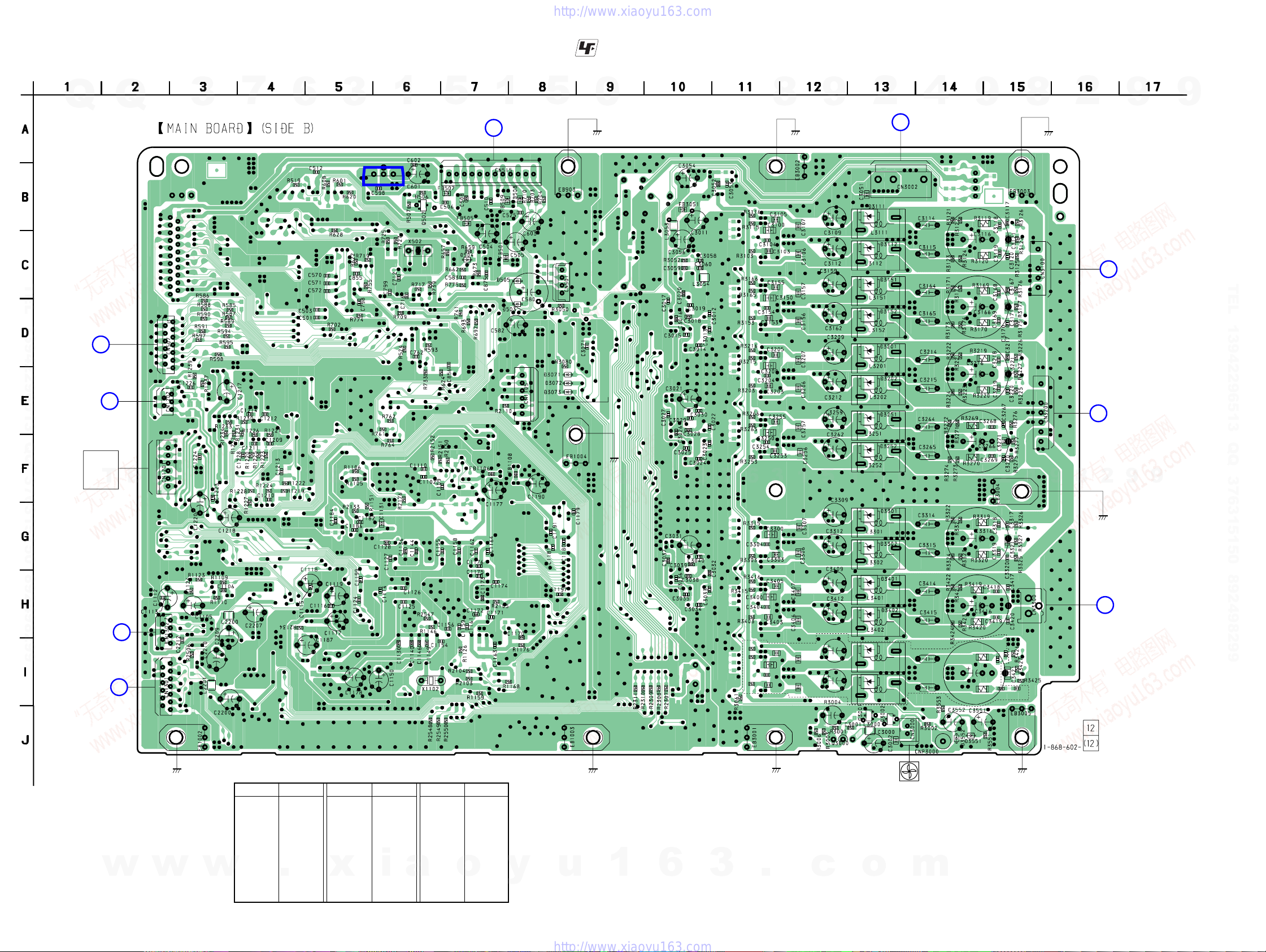
6-7. PRINTED WIRING BOARD – MAIN BOARD (SIDE B) –
3
7
9
4
6
2
Q
TEL 13942296513 QQ 376315150 892498299
IO-S TERMINAL BOARD
CN301
(Page 43)
E
D
MS-203 BOARD
CN001
(Page 49)
SPINDLE
MOTOR
SLED
T
MOTOR
Q
E
L
3
1
5
6
1
1
• See page 25 for Circuit Boards Location.
3
IC516
1
2
9
6
1
3
5
:Uses unleaded solder.
5
12
E
1
3
1
POWER BOARD
F
CN904
(Page 50)
1
6
5
1
for SOFT JIG
0
(CHASSIS) (CHASSIS)
4
1
for DIAG JIG
(CHASSIS)
6
7
Q
Q
3
8
3
1
9
5
2
POWER BOARD
G
(Page 50)
31
0
5
1
4
CN902
8
9
9
2
8
(CHASSIS)
1
4
1
6
4
9
2
8
I
SPEAKER BOARD
J
2
9
SPEAKER BOARD
CN301
(Page 48)
CN303
(Page 48)
9
9
TEL 13942296513 QQ 376315150 892498299
9
IO-S TERMINAL BOARD
CN304
(Page 44)
IO-S TERMINAL BOARD
CN201
(Page 44)
C
B
w
13
1
w
• Semiconductor Location
w
Ref. No.
D503 D-8
D504 C-7
D505 C-8
D3071 E-8
D3072 E-8
D3073 E-8
D3111 B-13
D3112 C-13
D3151 C-13
D3152 D-13
Location
.
Ref. No.
D3201 D-13
D3202 E-13
D3251 E-13
D3252 F-13
D3301 G-13
D3302 G-13
D3401 H-13
x
D3402 H-13
D3501 I-13
D3502 I-13
Location
i
Ref. No.
D3551 J-14
D3552 J-14
IC516 B-6
Q502 B-6
Q3000 J-12
a
Q3001 J-13
Q3002 J-13
Q3081 D-9
Location
o
y
u
(CHASSIS)
2
1
R3516
C3505
R3515
C3500
C3504
R3503
C3503
DZ620K
(CHASSIS)(CHASSIS)
1
6
3
(CHASSIS)
.
C3507
C3506
C3509
C3512
c
E
o
L3501
L3502
E
D3501
D3502
E
2
1
FAN
C3514
C3515
m
C3516
R3519
R3520
C3518
C3519
C3517
C3520
(CHASSIS)
SPEAKER BOARD
K
CN302
(Page 48)
HCD-DZ520K/DZ620K
3232
HCD-DZ520K/DZ620K
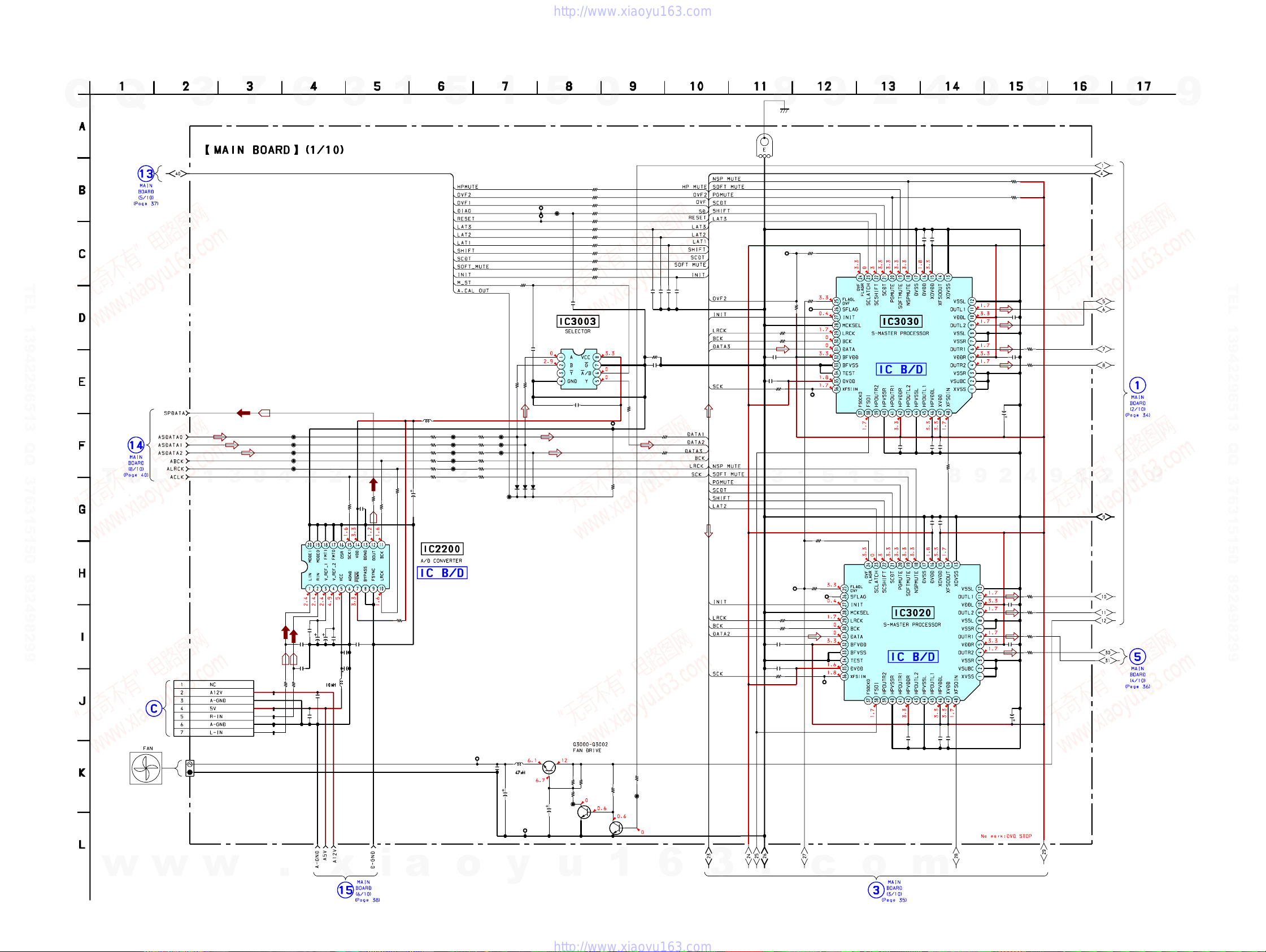
6-8. SCHEMATIC DIAGRAM – MAIN BOARD (1/10) –
Q
Q
3
7
6
3
• See page 52 for IC Block Diagrams.
1
TEL 13942296513 QQ 376315150 892498299
ICT501
ICT502
ICT503
ICT510
ICT511
T
E
L
1
3
9
4
2
2
R2211
9
6
R2212
100
100
C2211
0.1
R2213
100
R2214
100
5
L2201
0
R2311
R2310
R2309
R2308
R2307
R2306
C2200
10 50V 7L
1
5
ICT504
0
ICT505
0
ICT506
ICT512
0
ICT513
0
0
3
R2319
R2318
R2317
R2316
R2315
R2314
0
0
0
0
0
0
1
ICT507
ICT508
ICT5090
ICT3062
TP3003
TP3004
R3097
100
C3073
0.1
16V
100
100
R3078
R3077
D3071
D3072
1SS355WTE-17
5
D3073
1SS355WTE-17
1SS355WTE-17
ICT3063
C3071
0.1
TC7WH157FK
IC3003
C3072
0.1 16V
R3062
R3063
R3064
R3065
R3066
R3067
R3068
R3069
R3070
R3071
R3072
R3073
0
100
1k
1k
1k
100
100
100
100
100
100
100
100
TP3002
Q
R3080
100k
100
R3079
R4002
Q
100p
C3067
C3075
0.0047
R3075
R3076
9
2
8
2
9
9
9
TEL 13942296513 QQ 376315150 892498299
9
IC3030
CXD9788AR
C3038
0.1
25V
0
4
C3035
0.1
25V
C3039
0.1
25V
C3025
0.1
25V
C3034
0.1
25V
C3040
0.1
25V
C3024
0.1
25V
8
R3057
9
C3031
100
9
8
R3060
10k
R3059
10k
C3033
0.1 25V
R3301
100
C3032
0.1 25V
R3302
100
47
16V
4
2
1
R3031
R3032
TP3033
470
470
TP3032
R3021
470
1/10W
9
5
8
(CHASSIS)
EB3001
TERMINAL BOARD
TP3031
0.001
100p
100p
C3070
C3068
C3069
0
100
100
6
7
3
C3036
R3033
10k
R3034
100
100
R3035
0.1
25V
C3037
0.1 25V
R3037
100
3
1
2
5
IO-S TERMINAL BOARD
CN304
(Page 45)
w
w
CN1302
7P
FFC 1MM
CN3000
2P
w
R2203 R2202
470 470
TP581
TP582
TP580
TP577
TP579
.
IC2200
IC PCM1803DBR
C2205
0.1
C2202
0.01
C2201
0.01
C2212
0.1
C2210
7L
50V
C2209
10
C2213
0.001
7L
0.1
C2204
50V
10
L2200
x
C2206
C2207
C2208
47
16V
7L
R3022
TP3021
470
1/10W
TP3022
R3023
100
100
.
C3026
C3027
R3026
R3024
0.1 25 V
0.1 25 V
100
TP3023
c
o
CXD9788AR
C3028
0.1
25V
IC3020
C3029
0.1
25V
C3030
0.1 25V
m
R2200
i
100
a
TP3001
o
C3002
0.1
50V
L3000
C3000
100
16V
TP3000
y
Q3000
2SD1616-TP-LK
C3001
47
16V
R3006
2.2k
R3004
1.2k
ICT3001
Q3001
2SC3052EF
-T1-LEF
u
R3003
1.5k
R3001
10k
1
R3002
10k
ICT3002
Q3002
2SC3052EF-T1-LEF
6
3
0
0.1
C3021
16V
R3251
100
C3023
0.1 25V
R3252
100
R3201
100
C3022
0.1 25V
R3202
100
47
HCD-DZ520K/DZ620K
3333
HCD-DZ520K/DZ620K
6-9. SCHEMATIC DIAGRAM – MAIN BOARD (2/10) –
ICT3060
ICT3061
7
R3061
0
Q
Q
3
TEL 13942296513 QQ 376315150 892498299
T
E
L
1
3
9
4
• See page 52 for IC Block Diagrams.
6
C3403
0.1
16V
R3403
R3404
R3402 100
R3401 100
R3415
C3400
R3416
0.1 16V
R3315
R3316
C3253
0.1 16V
R3253
R3265
C3250
R3266
C3404
0.1
25V
C3405
C3303
0.1 16V
R3303
10
R3304
2
C3304
ICT3018
10
C3300
10
10
C3255
0.1 16V
3
ICT3010
ICT3011
10
TP3410 C3412
0
R3407
12k
ICT3012
10
ICT3013
0.1 50V
10
ICT3014
ICT3015
ICT3016
ICT3017
TP3310 C3312
0
2
9
R3307
12k
0.1
25V
ICT3019
0.1 50V
10
C3305
0.1 16V
ICT3020
ICT3021
ICT3022
TP3250 C3262
0
R3254
R3257
12k
C3254
0.1
25V
ICT3023
10
ICT3024
0.1 50V
ICT3025
ICT3026
6
1
IC3400
CXD9883M
5
IC3300
CXD9883M
IC3250
CXD9883M
C3407
0.033 50V
1
C3307
0.033 50V
C3257
0.033 50V
5
C3406
0.033
50V
P6SMBJ33A-5
P6SMBJ33A-5
C3306
0.033
50V
3
P6SMBJ33A-5
P6SMBJ33A-5
C3256
0.033
50V
P6SMBJ33A-5
P6SMBJ33A-5
D3402
D3401
D3302
D3301
D3252
D3251
C3413
C3408
C3313
C3308
0.1
50V
C3263
C3258
C3266
2200
35V
0.1
50V
0.1
50V
0.1
50V
C3316
0.1
50V
0.1
50V
2200
35V
L3402
L3401
L3302
L3301
L3252
L3251
1
100
35V
C3414
C3409
100
35V
C3416
2200
35V
100
35V
C3314
C3309
100
35V
100
35V
C3264
C3259
100
35V
C3415
50V
50V
C3315
50V
50V
C3265
50V
50V
5
1
1
C3420
C3419
R3420
R3419
C3418
C3417
1
1
1
1
C3320
C3319
R3320
R3319
C3318
C3317
C3270
C3269
R3270
R3269
C3268
C3267
0
1SS355WTE-17
0.0022 50V B
0.0022 50V B
2.7 1/8W
2.7 1/8W
0.0022 50V B
0.0022 50V B
0.0022 50V B
0.0022 50V B
2.7 1/8W
2.7 1/8W
0.0022 50V B
0.0022 50V B
2SC3052EF-T1-LEF
0.0022 50V B
0.0022 50V B
2.7 1/8W
2.7 1/8W
0.0022 50V B
0.0022 50V B
C3551
R3551
100k
1/10W
D3552
Q3551
1 50V
C3552
10
50V
R3553
10k
1/10W
Q
D3551
TE-17
S355W
1S
Q
DZ620K
R3554
100k
1/10W
27.8 11.9 11.9
R3555
C3555
0.1
8
001
32
3232
7
3
100k
1/10W
R3327
100k
0
1/10W
ICT3051
C3321
2.2
16V
F
2SA1235TP-1EF
16.316.316.316.316.316.3
3
6
R3325R3326
100k
1/10W
ICT3052 ICT3053 ICT3054
Q3302
2SA1235TP-1EF
Q3301
9
2.4
R3426 R3425
100k
1/10W
1
3.3
R3427
1/10W
C3421
10V
100k
10
F
0
3232
5
11.9
0
32
100k
1/10W
Q3401
2SA1235TP-1EF
27.8
1/10W
1/10W
1/10W
10k
10k
10k
1
R3324
R3322
R3321
Q3402
2SA1235TP-1EF
2
1/10W
1/10W
10k
10k
5
R3422
R3323
1/10W
10k
R3421
1/10W
10k
0
R3424
1/10W
10k
R3423
4
C3422
0.001 50V B
C3423
0.001 50V B
TP3304
TP3303
TP3302
TP3301
EB3005
TERMINAL BOARD
8
EB3004
TERMINAL BOARD
9
9
CN3300
2P
VH
BOARD IN
2
(CHASSIS)
(CHASSIS)
8
4
9
48
2
8
2
9
9
9
TEL 13942296513 QQ 376315150 892498299
9
w
HCD-DZ520K/DZ620K
w
w
.
x
i
a
o
y
u
1
6
3434
3
.
c
o
m
HCD-DZ520K/DZ620K
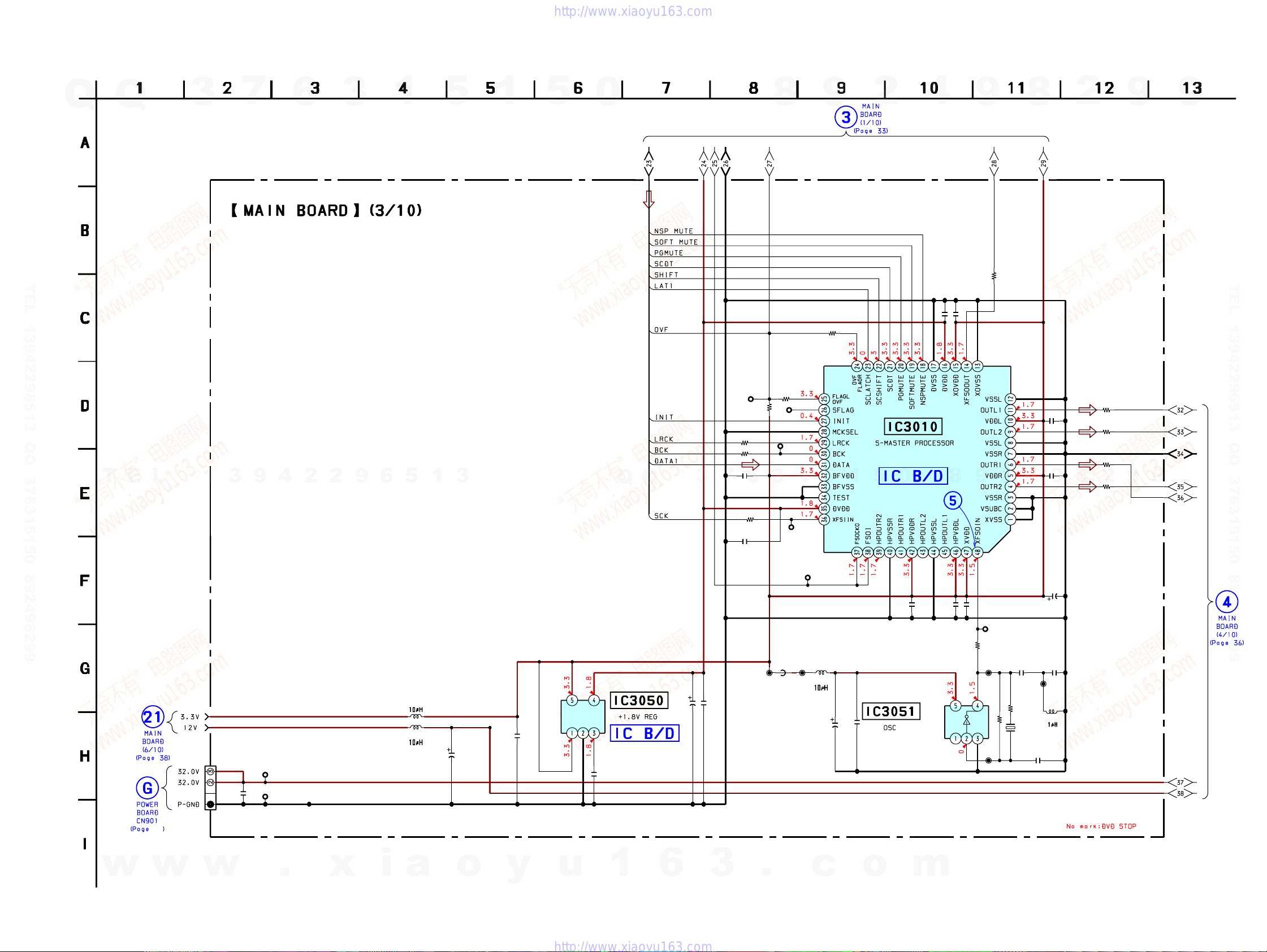
6-10. SCHEMATIC DIAGRAM – MAIN BOARD (3/10) –
Q
Q
3
7
6
3
• See page 25 for Waveform. • See page 52 for IC Block Diagrams.
1
TEL 13942296513 QQ 376315150 892498299
T
E
L
1
3
9
4
2
2
9
6
5
1
5
3
1
5
0
Q
Q
3
7
R3014
R3015
C3016
0.1 25V
TP3011
R3013
1/10W
6
9
2
C3013
0.1 25V F
R3101
C3012
0.1 25V F
8
R3151
100
R3152
100
2
R3102
100
100
9
9
9
TEL 13942296513 QQ 376315150 892498299
9
IC3010
CXD9788AR
0
4
C3015
0.1
25V
C3014
8
0.1
25V
9
9
R3055
100
2
8
4
1
2
5
R3011
1
9
470 1/10W
5
8
R3012
470
1/10W
10k
TP3012
100
100
TP3013
3
R3017
100
C3017
0.1 25 V
ICT3006
B
L3051
10V
IC3050
CN3002
3P
JST VH 3.96MM
51
C3051
0.1
50V
TP3053
TP3054
B
L3052
C3091
220
16V
1
C3052
TK11118CSCL-G
C3053
0.001 50V B
C3054
16V
25V
C3055
100
0.01
FB3051
0
TP3014
TP3015
ICT3007
L3053
C3056
220
10V
B
25V
C3057
0.01
C3018
0.1 25 V F
F
F
25V
25V
C3020
C3019
0.1
0.1
IC3051
SN74AHC1GU04DCKR
R3054
22
ICT3008
ICT3064
TP3056
1/10W
1M
R3052
C3059
0.001
50V
B
ICT3009
R3053
100
1/10W
X3051
49.152
SMD-49TB
5p 50V CH
C3058
C3011
16V
C3060
10p
50V
CH
L3054
47
w
HCD-DZ520K/DZ620K
w
w
.
x
i
a
o
y
u
1
6
3
3535
.
c
o
m
HCD-DZ520K/DZ620K
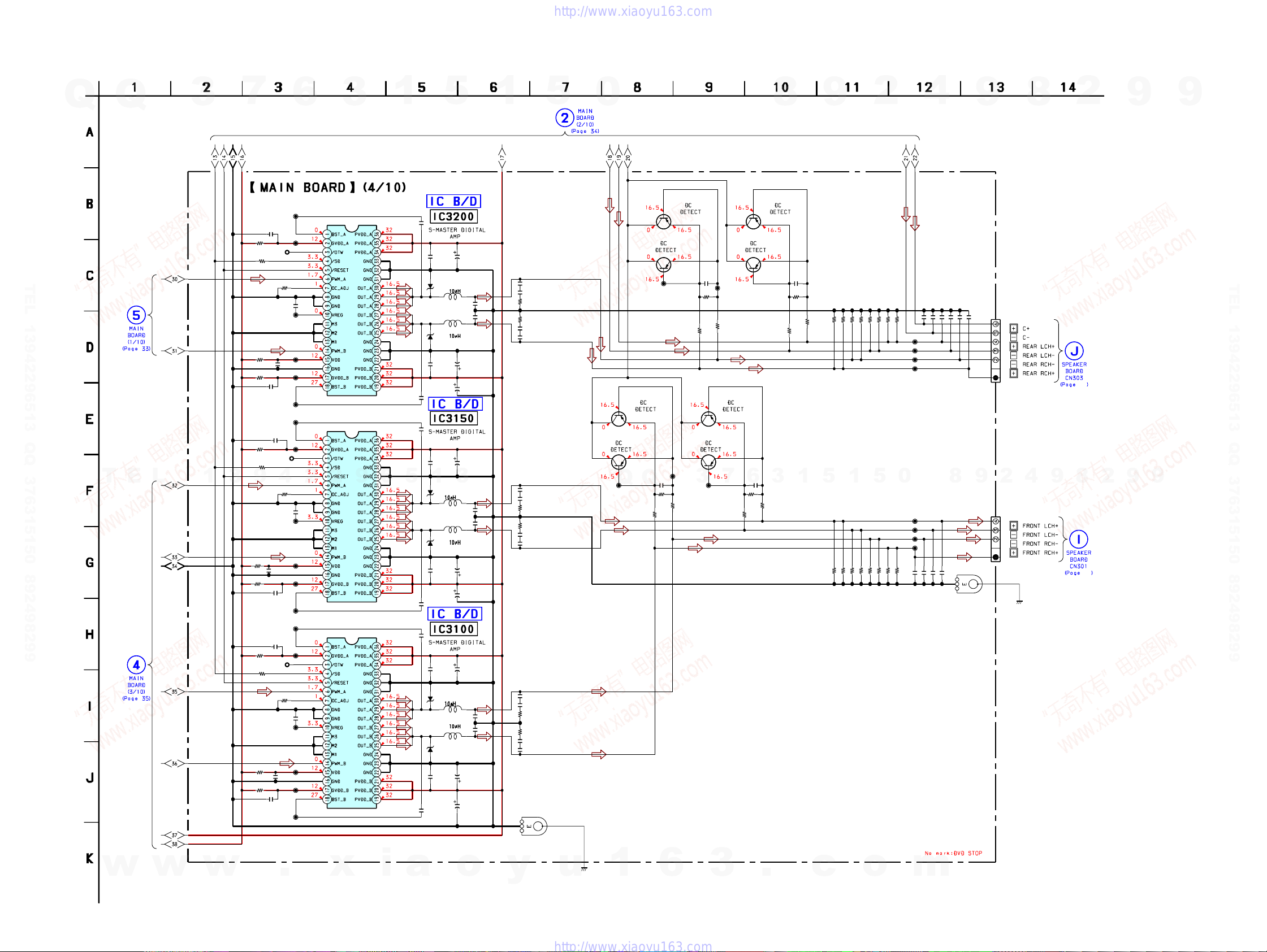
6-11. SCHEMATIC DIAGRAM – MAIN BOARD (4/10) –
3
7
C3203
0.1 16V
ICT3028
R3203
TP3210
10
0
R3204
R3207
12k
C3204
0.1 25V F
ICT3029
R3215
10
ICT3030
0.1 50V
C3200
R3216
10
ICT3031
C3205
0.1 16V
ICT3032
ICT3033
C3153
0.1 16V
R3153
ICT3034
TP3150 C3162
10
R3154
0
9
4
R3157
12k
C3154
0.1 25V
ICT3035
R3165
10
ICT3036
ICT3037
0.1 50V
C3150
R3166
10
C3155
0.1 16V
ICT3038
ICT3039
C3103
0.1 16V
R3103
ICT3040
10
TP3110 C3112
0
R3104
Q
Q
3
TEL 13942296513 QQ 376315150 892498299
T
E
L
1
• See page 52 for IC Block Diagrams.
6
ICT3027
2
2
3
IC3200
CXD9883M
9
IC3150
CXD9883M
6
1
C3206
0.033
50V
C3207
0.033 50V
C3156
0.033
50V
5
C3106
0.033
50V
C3213
D3202
P6SMBJ33A-5
D3201
P6SMBJ33A-5
1
D3152
P6SMBJ33A-5
D3151
P6SMBJ33A-5
C3157
0.033 50V
0.1
50V
C3208
C3163
C3158
C3113
0.1
50V
0.1
50V
0.1
50V
0.1
50V
5
L3202
L3201
3
L3152
L3151
C3212
C3209
C3216
100
35V
C3159
100
35V
C3166
100
35V
2200
100
35V
C3215
C3214
100
35V
2200
35V
C3165
C3164
35V
1
1
50V
1
50V
1
50V
1
50V
C3220
C3219
R3220
R3219
C3218
C3217
C3170
C3169
R3170
R3169
C3168
C3167
5
0.0022 50V B
0.0022 50V B
2.7 1/8W
2.7 1/8W
0.0022 50V B
0.0022 50V B
0.0022 50V B
0.0022 50V B
2.7 1/8W
2.7 1/8W
0.0022 50V B
0.0022 50V B
0
2SA1235TP-1EF
ICT3057
Q3101
Q
2SA1235TP-1EF
Q3102
2SA1235TP-1EF
Q
R3127
100k
1/10W
R3126
100k
1/10W
Q3201
ICT3055
C3121
2SA1235TP-1EF
2.2
16V
F
ICT3058
R3125
100k
1/10W
Q3202
R3227
100k
1/10W
R3226
1/10W
100k
C3221
2.2
16V
F
Q3151
2SA1235TP-1EF
3
ICT3059
2SA1235TP-1EF
ICT3056
R3225
100k
1/10W
Q3152
2SA1235TP-1EF
7
R3177
100k
1/10W
R3176
100k
1/10W
Q3251
C3171
2.2
16V
6
2SA1235TP-1EF
F
R3175
1/10W
8
Q3252
R3277
100k
1/10W
R3276
100k
1/10W
3
100k
C3271
2.2
16V
F
1
R3275
100k
1/10W
9
1/10W
10k
R3221
5
1/10W
10k
R3174
1/10W
10k
R3222
1/10W
10k
R3173
1
1/10W
10k
R3172
1/10W
10k
R3224
1/10W
10k
R3223
1/10W
10k
R3171
2
1/10W
1/10W
10k
10k
R3271
R3272
5
1/10W
1/10W
10k
10k
R3123
R3124
1/10W
10k
R3274
1/10W
10k
R3122
1/10W
10k
R3273
0
TP3104
TP3103
TP3102
TP3101
1/10W
10k
R3121
C3122
4
B
50V
C3323
0.001
TP3204
TP3203
TP3202
TP3201
B
B
50V
50V
C3123
0.001
0.001
C3322
C3172
B
50V
0.001
B
50V
0.001
B
B
50V
50V
C3272
C3273
0.001
0.001
8
B
50V
TERMINAL BOARD
C3173
0.001
C3223
B
50V
0.001
EB3003
9
B
50V
C3222
0.001
CN3200
BOARD IN
9
CN3100
BOARD IN
8
2
9
9
TEL 13942296513 QQ 376315150 892498299
9
48
8
9
9
2
48
4P
SCN
4
2
4P
SCN
(CHASSIS)
w
HCD-DZ520K/DZ620K
w
w
R3116
R3115
C3104
0.1 25V F
10
C3100
10
C3105
0.1 16V
R3107
ICT3044
ICT3041
ICT3042
0.1 50V
ICT3043
.
12k
D3112
P6SMBJ33A-5
D3111
P6SMBJ33A-5
IC3100
CXD9883M
C3108
C3107
0.033 50V
x
i
a
C3115
L3112
1
50V
L3111
C3114
1
50V
C3109
0.1
100
50V
35V
C3116
2200
35V
o
TERMINAL BOARD
y
C3120
C3119
R3120
R3119
C3118
C3117
EB3002
0.0022 50V B
0.0022 50V B
2.7 1/8W
2.7 1/8W
0.0022 50V B
0.0022 50V B
u
(CHASSIS)
1
6
3
.
c
o
m
3636
HCD-DZ520K/DZ620K
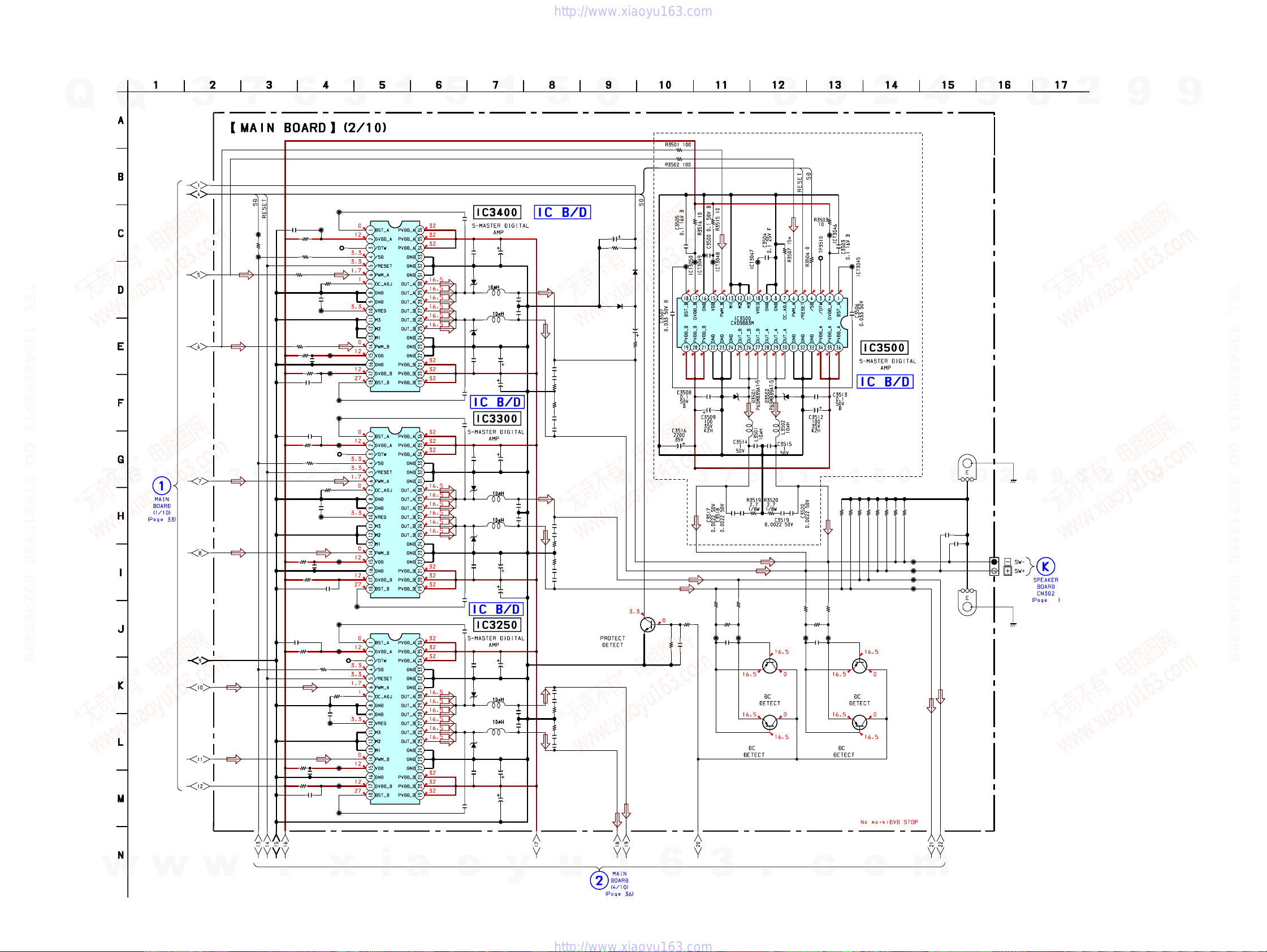
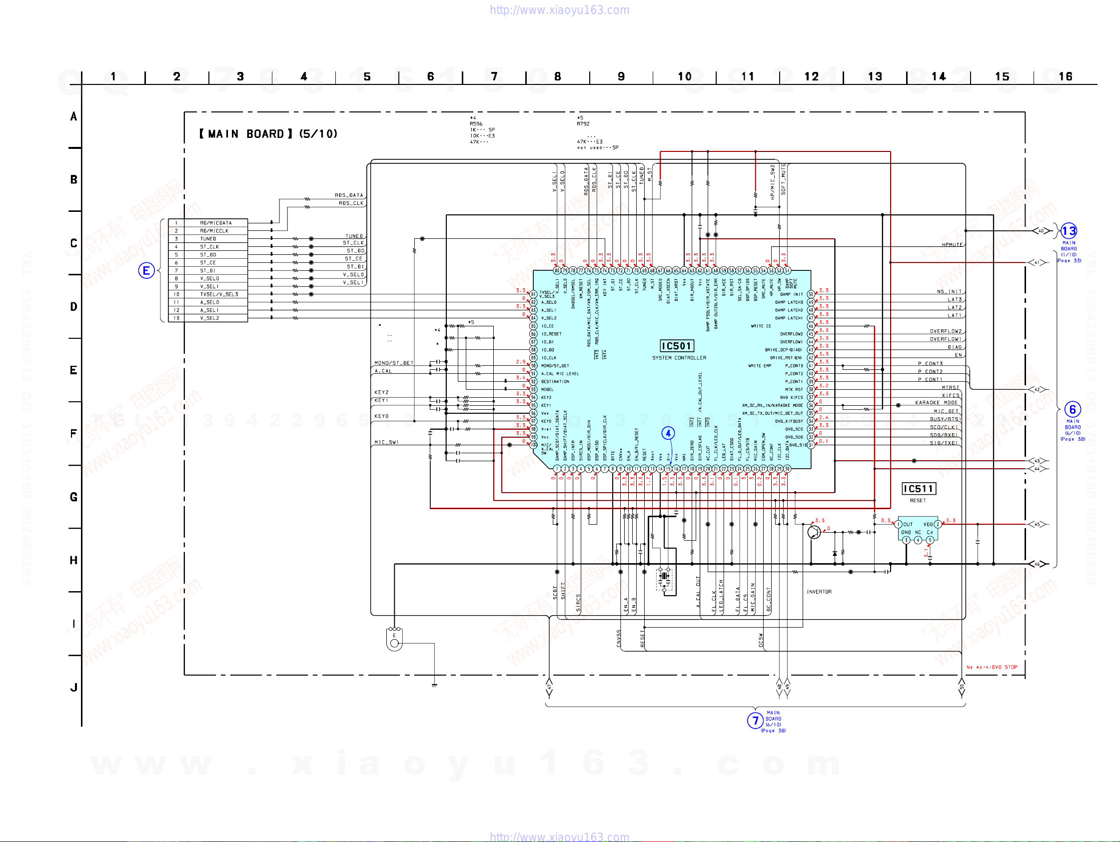
6-12. SCHEMATIC DIAGRAM – MAIN BOARD (5/10) –
CN507
FFC-S-1.0
3
13P
7
9
4
6
TP546
TP545
TP578
TP576
TP592
TP591
TP590
TP589
TP588
TP587
TP586
TP585
TP584
2
R598
R597
R595
R591
R594
R590
R589
R588
R586
R585
R587
2
R536
R535
100
100
100
100
100
100
100
100
100
100
100
Q
Q
3
TEL 13942296513 QQ 376315150 892498299
IO-S TERMINAL
BOARD
CN301
(Page 45)
T
E
L
1
• See page 25 for Waveform. • See page 55 for IC Pin Function Description.
ICT514
ICT515
ICT516
ICT517
ICT518
ICT519
ICT520
ICT521
1
6
3
1k
1k
9
5
6
R577
10k
15k
1
5
R774
1k
DZ520K
DZ620K
3
ICT580
C501
0.01 25V B
C503
0.01 25V B
C572
C571
C855
0.1
R622
10k
1
R596
R577
6
R702
10k
0.1
0.1
R755
C799
C798
C570
5
RU
0
1.5k RU
R524
4
9
8
R624
10k
C856
0.1
2
R756
1k
10k
R733
ICT535
R593
10k
ICT534
9
8
10k
10k
R744
0.1
C762
2
9
9
TEL 13942296513 QQ 376315150 892498299
R746
R792
R793
47k
R513
1k
TP792
R515
1k
TP793
100
R789
10k
R616
R790
100
10k
R614
100
R791
R612
10k
0.1
1k
0.1
0.1
ICT525
Q
Q
3
7
IC501
M30622MEP
-A76FPU0
6
3
1
5
1
5
0
8
10k
R742
10k
R741
10k
9
2
ICT548
4
ICT547
9
8
2
9
9
w
w
w
.
x
i
a
EB1001
TERMINAL BOARD
GROUND
o
(CHASSIS)
y
u
10k
R719
ICT581
1
10k
R708
10k
R720
6
10k
R709
ICT526
1k
1k
10k
10k
727
R
R726
R728
R725
3
0.1
C712
ICT527
X502
5MHz
R713
IC511
C875
0.01
IC PST3635NR
0.22 16V B
C587
C589
0.1
R657
4.7k
R729
4.7k
R730
R775
47k
47k
Q506
2SC3052EF
-T1-LEF
m
TE
D504
1SS355W
-17
C716
0.1
ICT528
R717
0
10k
R592
10k
.
ICT529
ICT530
10k
R739
c
ICT531
o
R662
47k
R659
100k
ICT532
ICT533
R673
10k
C583
0.22
16V
B
HCD-DZ520K/DZ620K
3737
 Loading...