

Page 1
HCD-DV2D
Amplifier section
AUDIO POWER SPECIFICATIONS
(USA model only)
POWER OUTPUT AND TOTAL HARMONIC
DISTORTION:
With 6 ohm loads, both channels dr i ven, from
120 – 10,000 Hz: rated 50 watts per channel
minimum RMS power, with no more than 10%
total harmonic distortion from 250 milliwatts to
rated output.
North American model:
Front speaker
Continuous RMS power output (reference):
50 + 50 watts (6 ohms at
1kHz, 10% THD)
Total harmonic distortion less than 0.07% (6 ohms at
1kHz, 25 W)
European and Russian models:
DIN power output (rated): 40 + 40 watts (6 ohms at
1kHz, DIN)
Continuous RMS power output (reference):
50 + 50 watts (6 ohms at
1kHz, 10% THD)
Music power output (reference):
100 + 100 watts (6 ohms at
1kHz, 10% THD)
Korean model:
The following measured at AC 220 V, 60 Hz
DIN power output (rated) 35 + 35 watts
(6 ohms at 1 kHz, DIN)
Continuous RMS power output (reference)
45 + 45 watts
(6 ohms at 1 kHz, 10%
THD)
Other models:
The following measured at AC 120 V, 240 V, 50/60 Hz
DIN power output (rated) 40 + 40 watts
(6 ohms at 1 kHz, DIN)
Continuous RMS power output (refe r en ce)
50 + 50 watts
(6 ohms at 1 kHz, 10%
THD)
Inputs
TV IN (phono jacks): voltage 1 V,
impedance 47 kilohms
Outputs
VIDEO OUT (phono jack) (except for European and
Russian models): max. output level
1 Vp-p, unbalanced, Sync
negative, load impedance
75 ohms
LINE-TV (European and Russian models onl y) :
max. output level 1 Vp-p,
unbalanced, Sync
negative, load impedance
75 ohms
DIGITAL OUT (OPTICAL) (Square optical connector
jack, rear panel)
Wavelength 660 nm
PHONES (stereo mini jack):
accepts headphones of
8ohms or more
SPEAKER: accepts impedance of
6ohms
Disc player section
System Compact disc and dig it a l
audio and video system
Laser Semiconductor laser
(DVD: λ=650 nm,
CD: λ=780 nm)
Emission duration:
continuous
Frequency response DVD (PCM 48 kHz):
2 Hz – 22 kHz (±1 dB)
CD: 2 Hz – 20 kHz (±1 dB)
Video color system format
Pan-American models:
NTSC
European and Russian
models: PAL
Other models: NTSC, PAL
SERVICE MANUAL
Ver. 1.2 2005.08
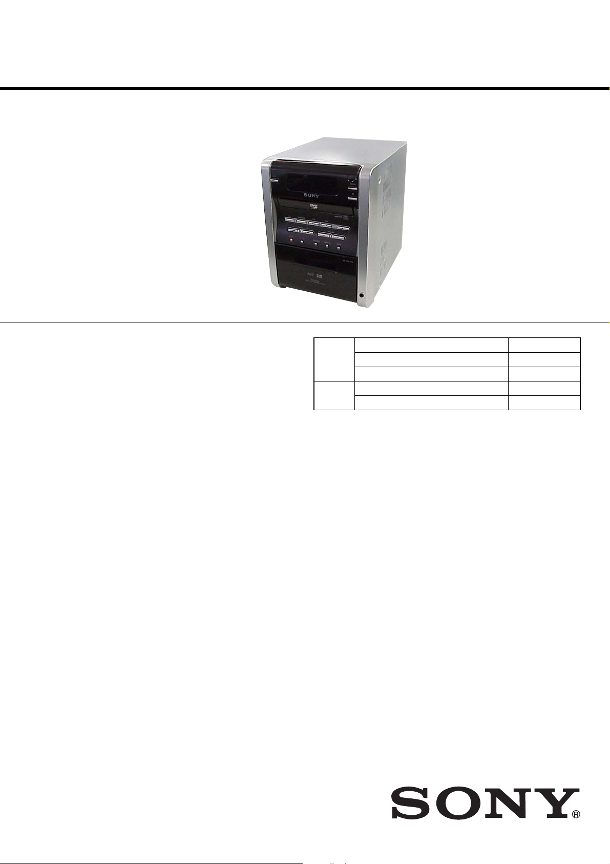
HCD-DV2D is the Amplifier, DVD player, Tape
Deck and Tuner section in CMT-DV2D .
This system incorporates Dolby1) Digital and DTS2) Digital
Surround System.
1)
Manufactured under license from Dolby Laboratories.
“Dolby”, “Pro Logic”, and the doub le-D symbol are trademarks
of Dolby Laboratories.
2)
Manufactured under license from Digital Theater Systems,
Inc. “DTS” and “DTS 2.0 + Digital Out” are trademarks of
Digital Theater Systems, Inc.
SPECIFICATIONS
DVD
Section
TAPE Model Name Using Similar Mechanism NEW
Section Tape Transport Mechanism T ype CMAL5Z220C
US Model
Canadian Model
AEP Model
UK Model
E Model
Australian Model
Model Name Using Similar Mechanism HCD-GP8D
DVD Mechanism Type KDA898ST
Traverse Mechanism Name 1ADOMEZ0412
9-879-536-03
2005H16-1
© 2005.08
Sony Corporation
Audio Group
Published by Sony Engineering Corporation
DVD DECK RECEIVER
— Continued on next page —
Page 2
HCD-DV2D
r
Ver 1.2
Tape deck section
Recording system 4-track 2-channel stereo
Frequency response 40 – 13,000 Hz,
using Sony TYPE I
cassette
Tuner section
FM stereo, FM/AM superheterodyne tuner
FM tuner section
Tuning range 87.5 – 108.0 MHz
(50 kHz step)
Antenna FM lead antenna
Antenna terminals 75 ohms unbalanced
Intermediate frequency 1 0.7 MHz
AM tuner section
Tuning range
Pan-American models: 530 – 1,710 kHz
(with the tuning interval
set at 10 kHz)
531 – 1,710 kHz
(with the tuning interval
set at 9 kHz)
European and Russian models:
531 – 1,602 kHz
(with the interval set at
9kHz)
Other models: 530 – 1,710 kHz
(with the interval set at
10 kHz)
531 – 1,602 kHz
(with the interval set at
9kHz)
Antenna AM loop antenna
Antenna terminals External antenna terminal
Intermediate frequency 4 50 kHz
SAFETY CHECK-OUT
After correcting the original service problem, perform the following
safety check before releasing the set to the customer:
Check the antenna terminals, metal trim, “metallized” knobs, screws,
and all other exposed metal parts for AC leakage.
Check leakage as described below.
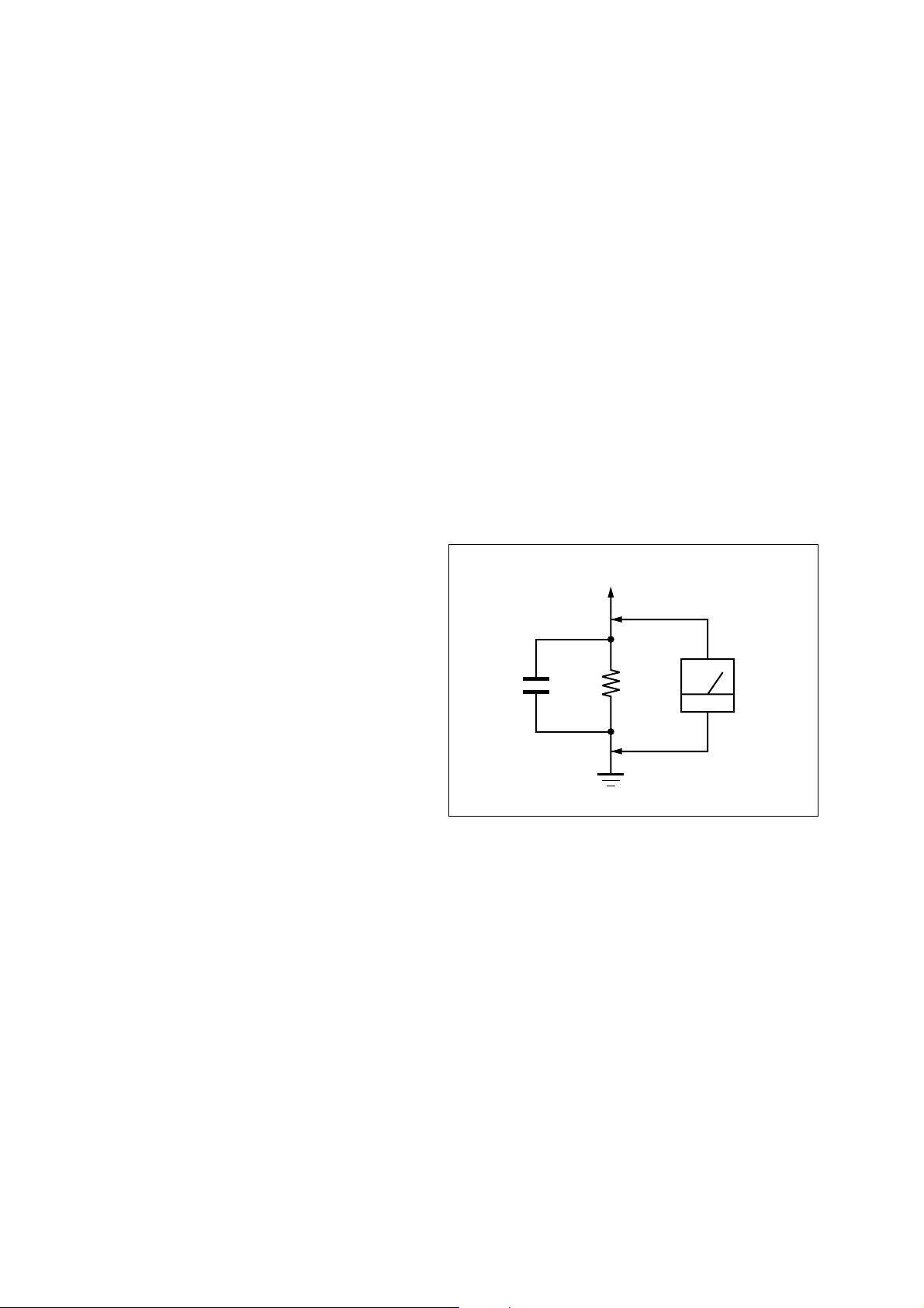
LEAKAGE TEST
The AC leakage from any exposed metal part to earth ground and
from all exposed metal parts to any exposed metal part having a
return to chassis, must not exceed 0.5 mA (500 microamperes.).
Leakage current can be measured by any one of three methods.
1. A commercial leakage tester, such as the Simpson 229 or RCA
WT -540A. Follow the manufacturers’ instructions to use these
instruments.
2. A battery-operated A C milliammeter. The Data Precision 245
digital multimeter is suitable for this job.
3. Measuring the voltage drop across a resistor by means of a
VOM or battery-operated AC v oltmeter . The “limit” indication
is 0.75 V, so analog meters must have an accurate low-v oltage
scale. The Simpson 250 and Sanwa SH-63Trd are examples
of a passive VOM that is suitable. Nearly all battery operated
digital multimeters that have a 2 V A C range are suitable. (See
Fig. A)
To Exposed Metal
Parts on Set
General
Power requirements
North American model: 120 V AC, 60 Hz
European and Russian models:
230 V AC, 50/60 Hz
Australian model: 230 – 240 V AC, 50/60 Hz
Taiwan model: 120 V AC, 50/60 Hz
Korean model: 220 V AC, 60 Hz
Other models: 110 – 120 V, 220 – 240 V
AC, 50/60 Hz
Adjustable with voltage
selector
Power consumption
USA model: 110 watts
Canadian model: 110 watts
European and Russian models:
110 watts
0.3 watts (in Power Saving
mode)
Other models: 120 watts
Dimensions (w/h/d) (excl. speakers)
Approx. 191 × 255 ×
310 mm
Mass (excl. speakers) Approx. 6.5 kg
Design and specifications are subject to change
without notice.
AC
0.15 µF
1.5 k
Ω
voltmete
(0.75 V)
Earth Ground
Fig. A. Using an AC voltmeter to check AC leakage.
SAFETY-RELATED COMPONENT WARNING!!
COMPONENTS IDENTIFIED BY MARK 0 OR DOTTED LINE
WITH MARK 0 ON THE SCHEMATIC DIAGRAMS AND IN
THE PARTS LIST ARE CRITICAL TO SAFE OPERATION.
REPLACE THESE COMPONENTS WITH SONY PARTS WHOSE
PART NUMBERS APPEAR AS SHOWN IN THIS MANUAL OR
IN SUPPLEMENTS PUBLISHED BY SONY.
ATTENTION AU COMPOSANT AYANT RAPPORT
À LA SÉCURITÉ!
LES COMPOSANTS IDENTIFIÉS PAR UNE MARQUE 0 SUR
LES DIAGRAMMES SCHÉMATIQUES ET LA LISTE DES
PIÈCES SONT CRITIQUES POUR LA SÉCURITÉ DE
FONCTIONNEMENT. NE REMPLACER CES COM- POSANTS
QUE PAR DES PIÈCES SONY DONT LES NUMÉROS SONT
DONNÉS DANS CE MANUEL OU D ANS LES SUPPLÉMENTS
PUBLIÉS PAR SONY.
2
Page 3

HCD-DV2D
Ver. 1.2
Laser component in this product is capable of emitting radiation
exceeding the limit for Class 1.
This appliance is classified as
a CLASS 1 LASER product.
The CLASS 1 LASER
PRODUCT MARKING is
located on the rear exterior.
CAUTION
Use of controls or adjustments or performance of procedures
other than those specified herein may result in hazardous radiation
exposure.
Notes on chip component replacement
• Never reuse a disconnected chip component.
• Notice that the minus side of a tantalum capacitor may be
damaged by heat.
Flexible Circuit Board Repairing
• Keep the temperature of the soldering iron around 270 °C
during repairing.
• Do not touch the soldering iron on the same conductor of the
circuit board (within 3 times).
• Be careful not to apply force on the conductor when soldering
or unsoldering.
UNLEADED SOLDER
Boards requiring use of unleaded solder are printed with the leadfree mark (LF) indicating the solder contains no lead.
(Caution: Some printed circuit boards may not come printed with
the lead free mark due to their particular size)
: LEAD FREE MARK
Unleaded solder has the following characteristics.
• Unleaded solder melts at a temperature about 40 °C higher
than ordinary solder.
Ordinary soldering irons can be used but the iron tip has to be
applied to the solder joint for a slightly longer time.
Soldering irons using a temperature regulator should be set to
about 350 °C.
Caution: The printed pattern (copper foil) may peel away if
the heated tip is applied for too long, so be careful!
• Strong viscosity
Unleaded solder is more viscou-s (sticky, less prone to flow)
than ordinary solder so use caution not to let solder bridges
occur such as on IC pins, etc.
• Usable with ordinary solder
It is best to use only unleaded solder but unleaded solder may
also be added to ordinary solder.
• Abbreviation
AUS: Australian model.
CND: Canadian model.
E2 : 120 V AC area in E model.
E3 : 240 V AC area in E model.
E51 : Chilean and Peruvian model.
KR : Korea model.
RU : Russian model.
SP : Singapore model.
TW : Taiwan model.
TABLE OF CONTENTS
1. SERVICING NOTES ................................................ 4
2. GENERAL ................................................................... 5
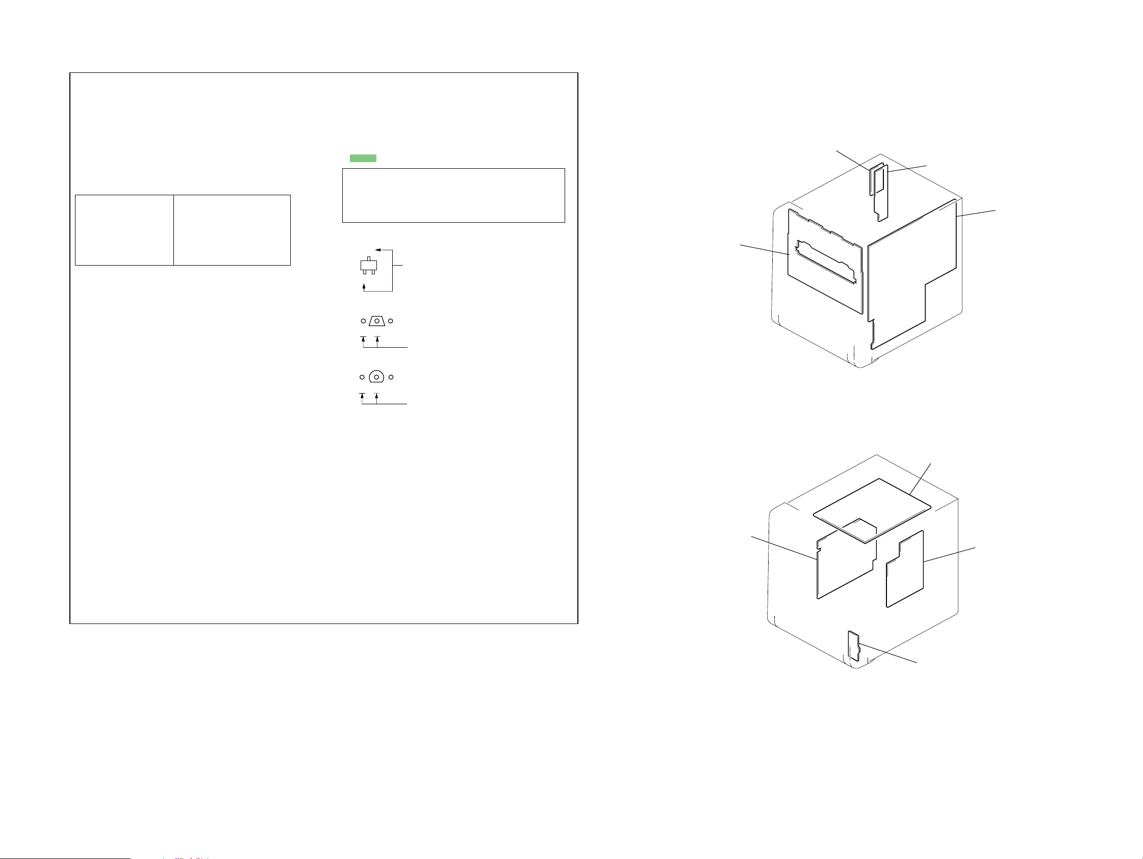
3. DISASSEMBLY
3-1. Disassembly Flow ........................................................... 8
3-2. Cover Top, DC Fan .......................................................... 9
3-3. AMP Board, AV Board, Tuner (FM/AM) ....................... 9
3-4. MPEG Board ................................................................... 10
3-5. DVD Mech Cover A/B .................................................... 10
3-6. Panel (DVD) .................................................................... 11
3-7. DVD Loader (KDA898ST) ............................................. 11
3-8. Front Panel Section ......................................................... 12
3-9. MAIN Board.................................................................... 12
3-10. Cassette Deck Mechanism (CMAL5Z220C) .................. 13
3-11. KEY Board ...................................................................... 13
3-12. Traverse Mech (1ADOMEZ0412) .................................. 14
3-13. Lid TC ............................................................................. 14
4. TEST MODE ............................................................... 15
5. MECHANICAL ADJUSTMENTS......................... 19
6. ELECTRICAL ADJUSTMENTS .......................... 19
7. DIAGRAMS
7-1. Block Diagrams — MPEG-1 Section — ....................... 22
— MPEG-2 Section —.................................................... 23
— AUDIO Section —...................................................... 24
— PANEL/POWER Section — ...................................... 25
7-2. Printed Wiring Board — MAIN Section-1 — ................ 26
7-3. Printed Wiring Board — MAIN Section-2 — ................ 27
7-4. Schematic Diagram — MAIN Section — ...................... 28
7-5. Printed Wiring Board — MPEG Section-1 — ............... 29
7-6. Printed Wiring Board — MPEG Section-2 — ............... 30
7-7. Schematic Diagram — MPEG Section — ..................... 31
7-8. Printed Wiring Board — KEY Section — ..................... 32
7-9. Schematic Diagram — KEY Section — ........................ 33
7-10. Printed Wiring Board — AV Section —......................... 34
7-11. Schematic Diagram — AV Section — ........................... 35
7-12. Printed Wiring Board — AMP,
POWER(EXCEPT AEP, UK, RU, KR, AUS) Section — 36
7-13. Schematic Diagram — AMP Section —........................ 37
7-14. Schematic Diagram — POWER Section
(E2, E3, E51, SP, TW Model) — .................................... 38
7-15. Schematic Diagram — POWER Section
(US, CND Model) — ...................................................... 39
8. EXPLODED VIEWS
8-1. Overall Section................................................................ 54
8-2. Front Panel Section ......................................................... 55
8-3. Chassis Section................................................................ 56
8-4. DVD Mechanism Deck Section ...................................... 57
9. ELECTRICAL PARTS LIST .................................. 58
3
Page 4
HCD-DV2D
Ver. 1.2
SECTION 1
SERVICING NOTES
NOTES ON HANDLING THE OPTICAL PICK-UP
BLOCK OR BASE UNIT
The laser diode in the optical pick-up block may suffer electrostatic
break-down because of the potential difference generated by the
charged electrostatic load, etc. on clothing and the human body.
During repair, pay attention to electrostatic break-down and also
use the procedure in the printed matter which is included in the
repair parts.
The flexible board is easily damaged and should be handled with
care.
NOTES ON LASER DIODE EMISSION CHECK
The laser beam on this model is concentrated so as to be focused on
the disc reflective surface by the objective lens in the optical pickup block. Therefore, when checking the laser diode emission,
observe from more than 30 cm away from the objective lens.
LASER DIODE AND FOCUS SEARCH OPERATION
CHECK
Carry out the “S curve check” in “CD section adjustment” and check
that the S curve waveforms is output three times.
DISC TRA Y LOCK
The disc tray lock function for the antitheft of an demonstration
disc in the store is equipped.
Procedure :
1. Press the ?/1 button to turn the set ON.
2. Press the DVD u button to select “DVD”
3. Set disc on the tray, press the x button and the Z button
simultaneously for five seconds.
4. The message “LOCKED” is displayed the tray is locked.
5. To release from this mode, press the x button and the Z
button simultaneously for five seconds again.
6. The message “UNLOCKED” is displayed and the tray is
unlocked.
Note: When “LOCKED” is displayed, the slot lock is not released by
turning power on/off with the ?/1 button.
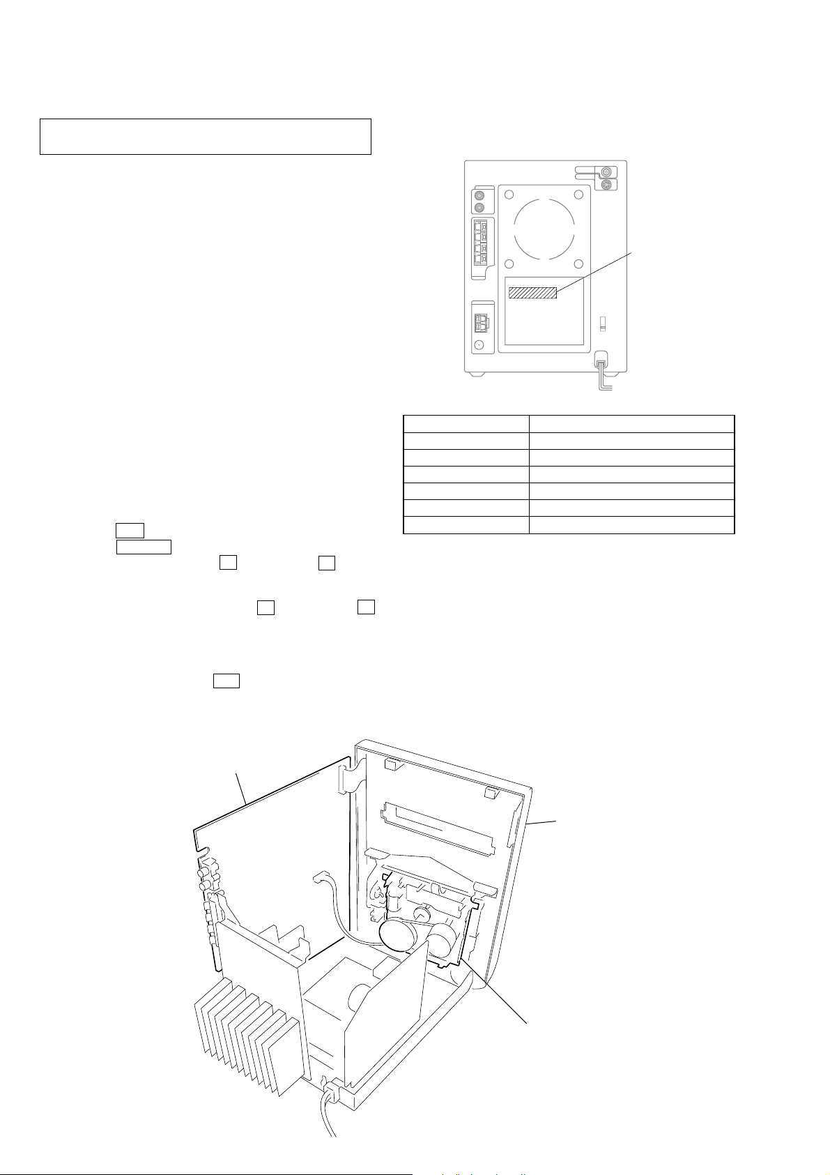
MODEL IDENTIFICATION
– Back Panel –
Model Power V oltage Indication
US, CND models 120 V AC, 60 Hz
AEP, UK, RU models 230 V AC, 50/60 Hz
SP, E2, E3, E51
TW model 120 V AC, 50/60 Hz
KR model 220 V AC, 60 Hz
AUS model 230 – 240 V AC, 50/60 Hz
•Abbreviation
AUS: Australian model.
CND : Canadian model.
E2 : 120 V AC area in E model.
E3 : 240 V AC area in E model.
E51 : Chilean and Peruvian model.
KR : Korea model.
RU : Russian model.
SP : Singapore model.
TW : Taiwan model.
models 110 – 120 V/220 – 240V AC, 50/60 Hz
Power requirement
indication
• SERVICE POSITION OF THE TAPE CASSETTE MECHANISM DECK
MAIN board
Front Panel
Tape Cassette Mechanism Deck
(CMAL5Z220C)
4
Page 5
SECTION 2
GENERAL
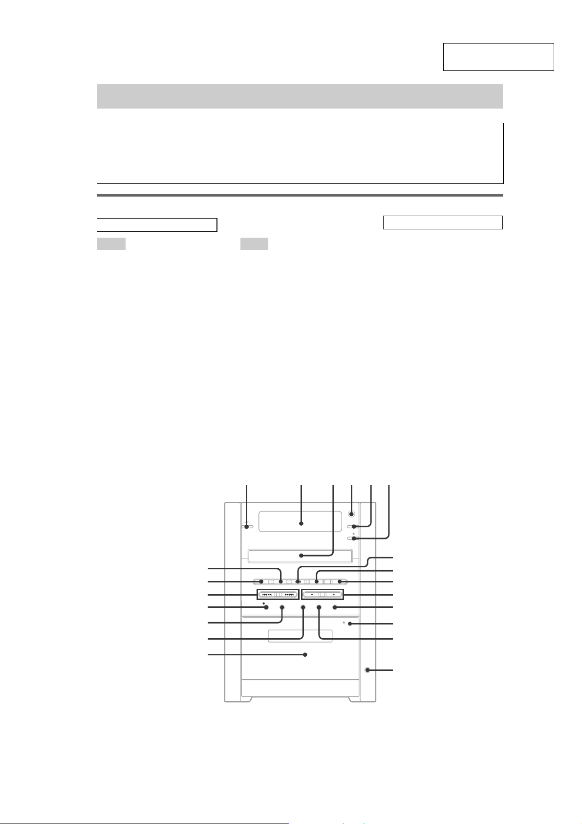
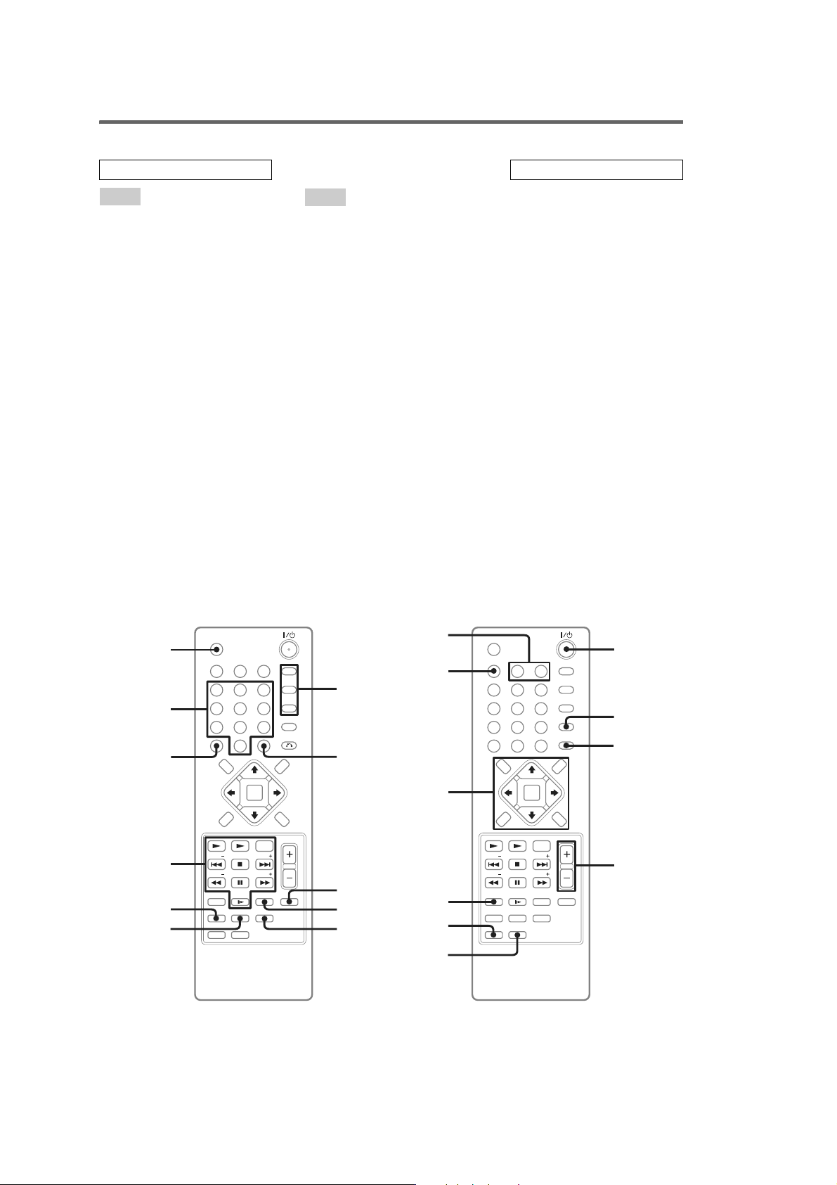
List of button locations and reference pages
HCD-DV2D
This section is extracted
from instruction manual.
How to use this page
Use this page to find the lo ca tio n of buttons and other
parts of the system that are mentioned in the text.
Main unit
ALPHABETICAL ORDER
A – O P – Z
Cassette compartment qh (28)
CD SYNC qk (28)
Disc tray 3 (12)
DISPLAY 5 (27, 34, 35, 36)
Display window 2
PHONES jack qf
PLAY MODE qj (13, 16, 44)
PRESET EQ qd (30)
Remote sensor 4
REPEAT
TUNER/BAND ws (25, 26, 29)
TUNING +/– w; (25, 27)
TV wa (29, 38)
VOLUME +/– 0 (13, 27, 28)
qa (15)
Illustration number
r
TUNER/BAND ws (25, 26, 29)
RR
Name of button/part Reference page
BUTTON DESCRIPTIONS
?/1 (power) 1 (10, 44)
Z (open/close) 6 (12)
DVD NX (play/pause) 7 (10,
12, 23, 28, 39, 44)
TAPE N (play) 8 (28)
x (stop) 9 (10, 12, 26, 28, 31,
39, 44)
Z PUSH OP E N (eject) qs (28)
z REC PAUSE/START (record)
ql (28, 31)
m/M (rewind/fast forward)
w; (13, 28)
./> (go back/forward) w;
(12, 28)
ws
wa
w;
ql
qk
qj
qh
123546
7
8
9
0
qa
qs
qd
qf
5
Page 6
HCD-DV2D
Remote control
ALPHABETICAL ORDER
A – J
ANGLE qa (20)
AUDIO qa (19, 31)
CLEAR ql (16, 17, 23)
CLOCK/TIMER SELECT 0
(33, 34)
CLOCK/TIMER SET 0 (11, 32,
33)
DIMMER 6 (34)
DISPLAY 8 (34, 35, 36)
DVD MENU 8 (14, 15)
DVD SETUP 8 (11, 20, 21, 22,
24, 38, 44)
DVD TOP MENU 8 (14)
ENTER 8 qs (11, 14, 15, 17, 20,
21, 22, 25, 32, 33, 38, 44)
FM MODE qh (27)
K – Z
KARAOKE PON qg (30)
MUTING 9 (13, 27, 28)
Number buttons* w; (14, 15, 16,
17, 22)
PLAY MODE 7 (13, 16)
PRESET +/– qk (25, 26)
PRESET EQ qf (30)
REPEAT qj (15)
SLEEP wa (32)
SUBTITLE qa (20)
TIME SEARCH 2 (17)
TUNER BAND qk (25, 26)
TUNER MEMORY 5 (25)
TUNING +/– qk (25, 27)
TV qd
VOLUME +/– 4 (13, 27, 28, 32)
BUTTON DESCRIPTIONS
?/1 (power) 1 (10, 32, 44)
O RETURN 3 (15)
M/m/</
TAPE N (play) qk (28)
DVD N (play) qk (10, 12, 23,
./> (go back/forward) qk
x (stop) qk (10, 12, 28, 39)
m/M (rewind/fast forward)
DVD X (pause) qk (12)
SLOW y qk (13)
*The number 5 button has a
, 8 (11, 13, 20, 38,
44)
39)
(11, 12, 32)
qk (13, 28)
tactile dot. Use the tactile dot as
a reference when operating the
system.
wa
w;
ql
qk
qj
qa
qs
qd
qf
qgqh
0
1
9
2
3
8
4
7
6
5
6
Page 7

Setting the clock
Use buttons on the remote for the operation.
1
Press ?/1 to turn on the system.
2
Press CLOCK/TIMER SET.
3
Press . or > repeatedly to set th e
hour.
4
Press ENTER.
5
Press . or > repeatedly to set the
minute.
6
Press ENTER.
The clock starts working.
To adjust the clock
1
Press CLOCK/TIMER SET.
2
Press . or > to select “CLOCK SET”,
then press ENTER.
3
Do the same procedures as step 3 to 6
above.
HCD-DV2D
Notes
The clock settings are canceled when you disconnect
the power cord or if a power failure occurs.
You cannot set the clock in Power Sa ving Mode
(page 34).
7
Page 8
HCD-DV2D
Ver. 1.2
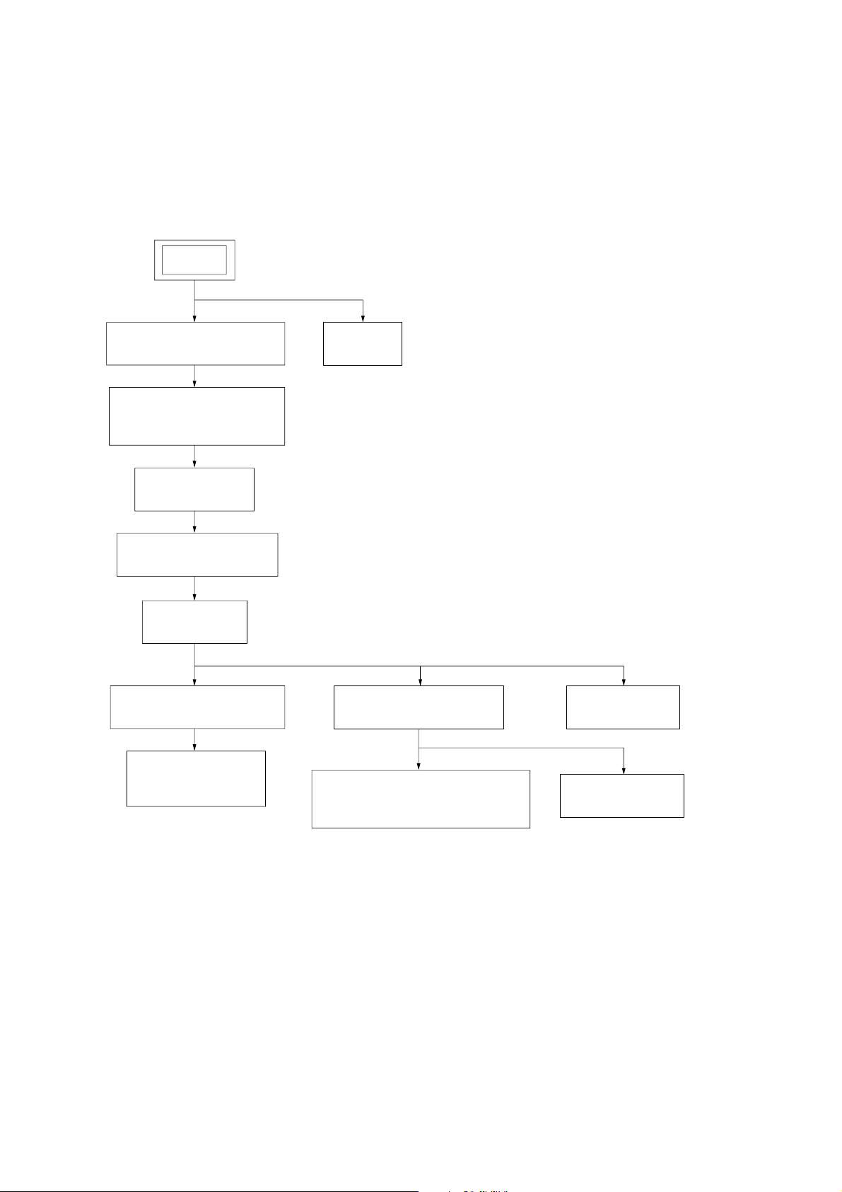
3-1. DISASSEMBLY FLOW
•This set can be disassembled in the order shown below.
SET
SECTION 3
DISASSEMBLY
3-2. COVER TOP, DC FAN
(Page 9)
3-3. AMP BOARD, AV BOARD,
TUNER (FM/AM)
(Page 9)
3-4. MPEG BOARD
(Page 10)
3-5. DVD MECH COVER A/B
(Page 10)
3-6. PANEL (DVD)
(Page 11)
3-7. DVD LOADER (KDA898ST)
(Page 11)
3-13. LID TC
(Page 14)
3-8. FRONT PANEL SECTION
(Page 12)
3-9. MAIN BOARD
(Page 12)
3-12. TRA VERSE MECH
(1ADOMEZ0412)
(Page 14)
3-10. CASSETTE DECK MECHANISM
(CMAL5Z220C)
(Page 13)
3-11. KEY BOARD
(Page 13)
8
Page 9
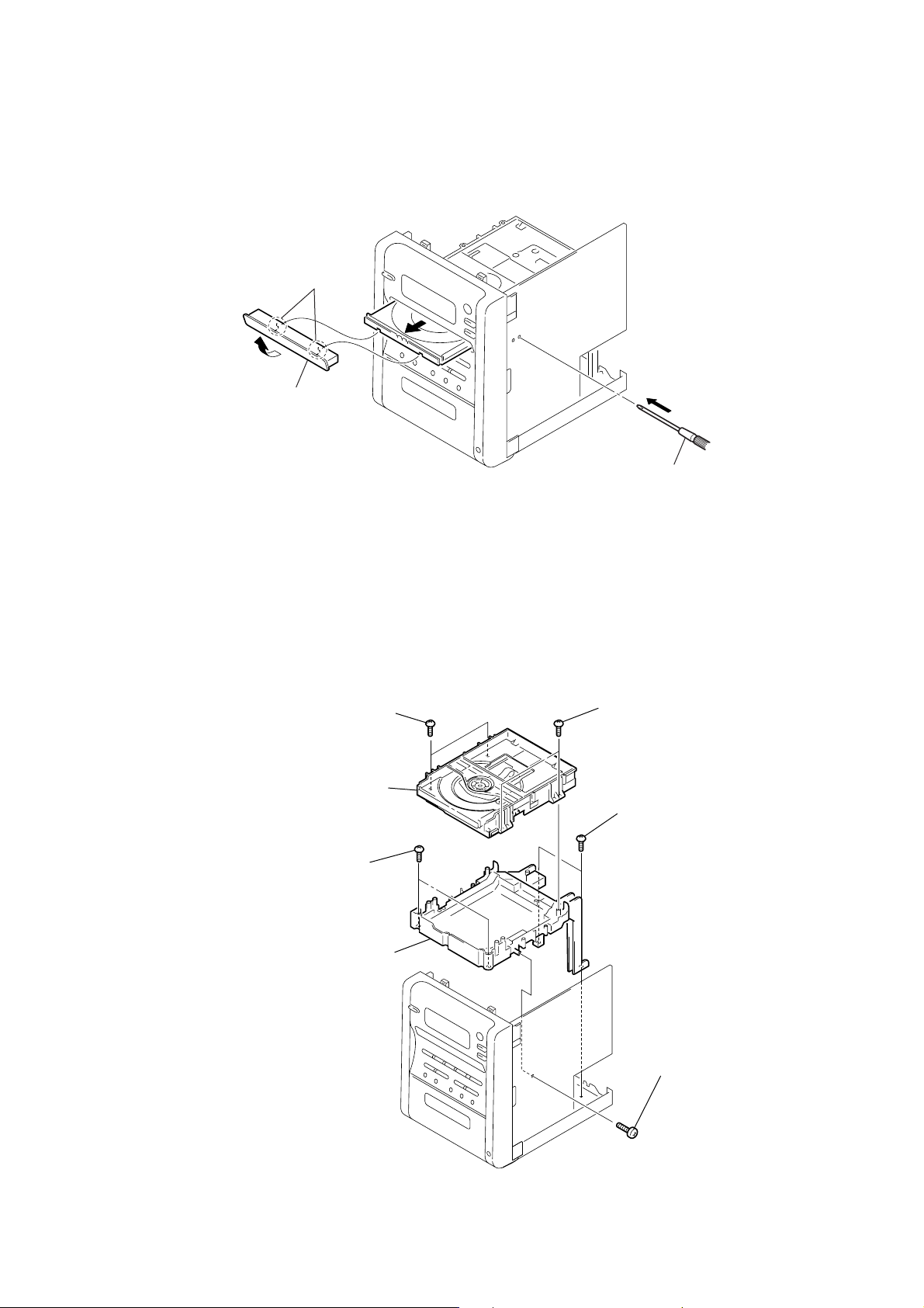
Note: Follow the disassembly procedure in the numerical order given.
)
3-2. COVER TOP, DC FAN
5
cover top
a
2
two s
(+BTP 3
crews
×
8)
b
4
3
five s
(+BTP 3
crews
8
connector
(3P)(CN350)
a
HCD-DV2D
×
8)
q;
7
s
(+BVTP 3
DC fan
9
four s
crew
crews
×
(+BVTP 3
×
8)
8)
6
two s
(+BVTP 3
crews
×
8
1
two s
(+BTP 3
crews
×
8)
3-3. AMP BOARD, AV BOARD, TUNER (FM/AM)
qh
qj
AV board
qs
wire (flat type)
(5core) (CN851)
two s
(+BVTP 3
b
crews
5
connector
(3P) (CN106)
×
10)
4
connector
(7P) (CN102)
qa
cover HT-SINK
3
connector
(10P) (CN108)
1
two s
(+BVTP 3
crews
×
10)
q;
s
crew
(+BTP 3
2
two s
qf
wire (flat type)
×
8)
(11core)
qa
earth wire
qk
two claws
qg
tuner
qd
(+BVTP 3
ql
panel back
6
connector
(5P) (CN101)
9
three s
(+BVTP 3
8
two s
(+BVTP 3
two s
crews
×
crews
8)
(+BVTP 3
7
AMP board
crews
×
10)
×
8)
crews
×
10)
9
Page 10
HCD-DV2D
)
Ver. 1.1
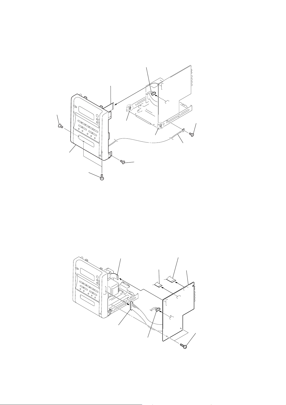
3-4. MPEG BOARD
7
wire (flat type)
(5core) (J703)
1
three s
(+BTP 3
4
wire (flat type)
(24core) (J705)
8
MPEG board
crews
×
8)
5
wire (flat type)
(9core) (J701)
6
connector
(9P) (J702)
3
wire (flat type)
(6core) (J706)
2
connector
(5P) (J707
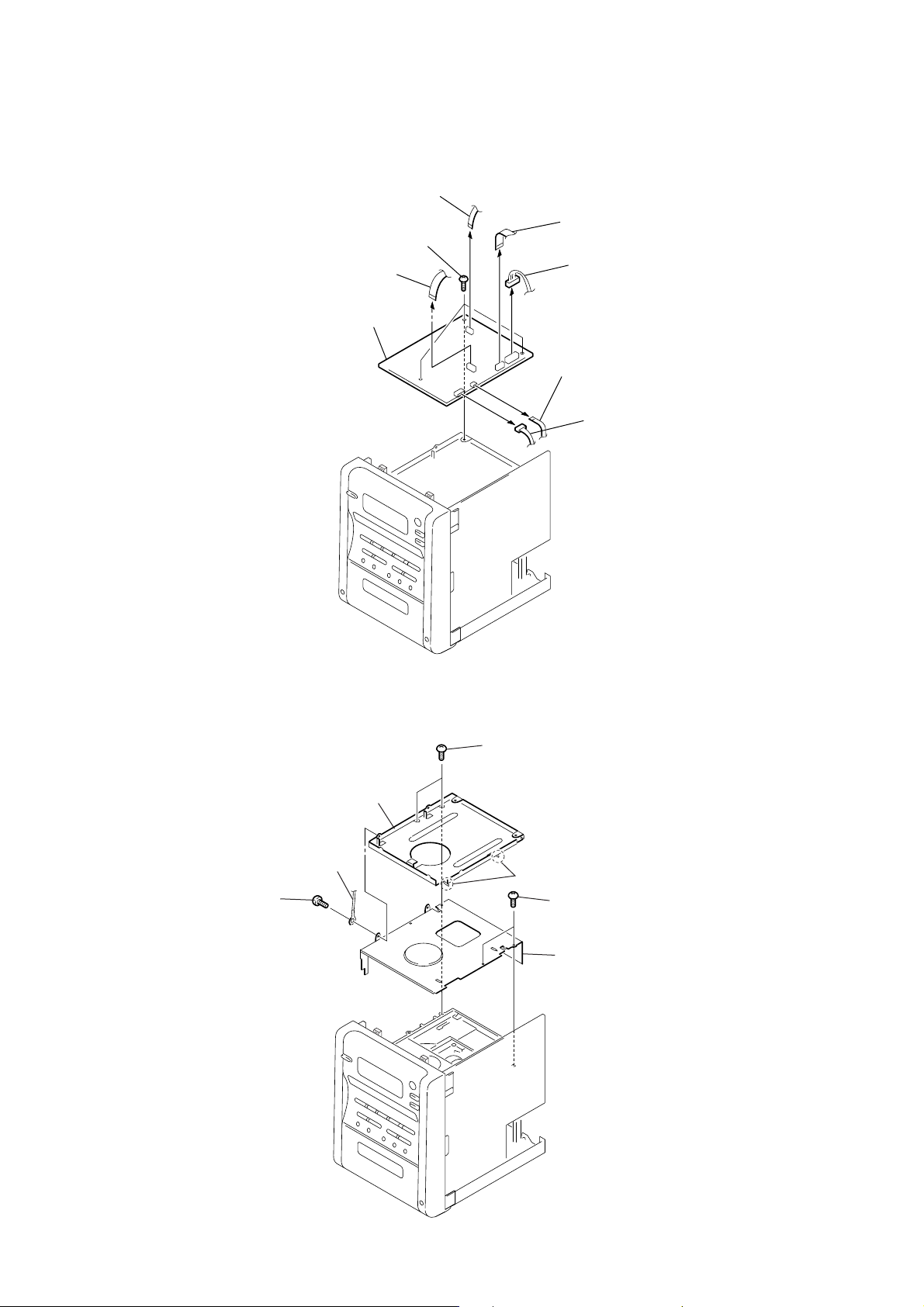
3-5. DVD MECH COVER A/B
1
s
crew
(+BTP 3
5
DVD mech cover A
2
earth wire
×
8)
3
two s
(+BTP 3
crews
4
two hooks
6
(+BVTP 3
×
8)
two s
crews
×
7
DVD mech cover B
8)
10
Page 11
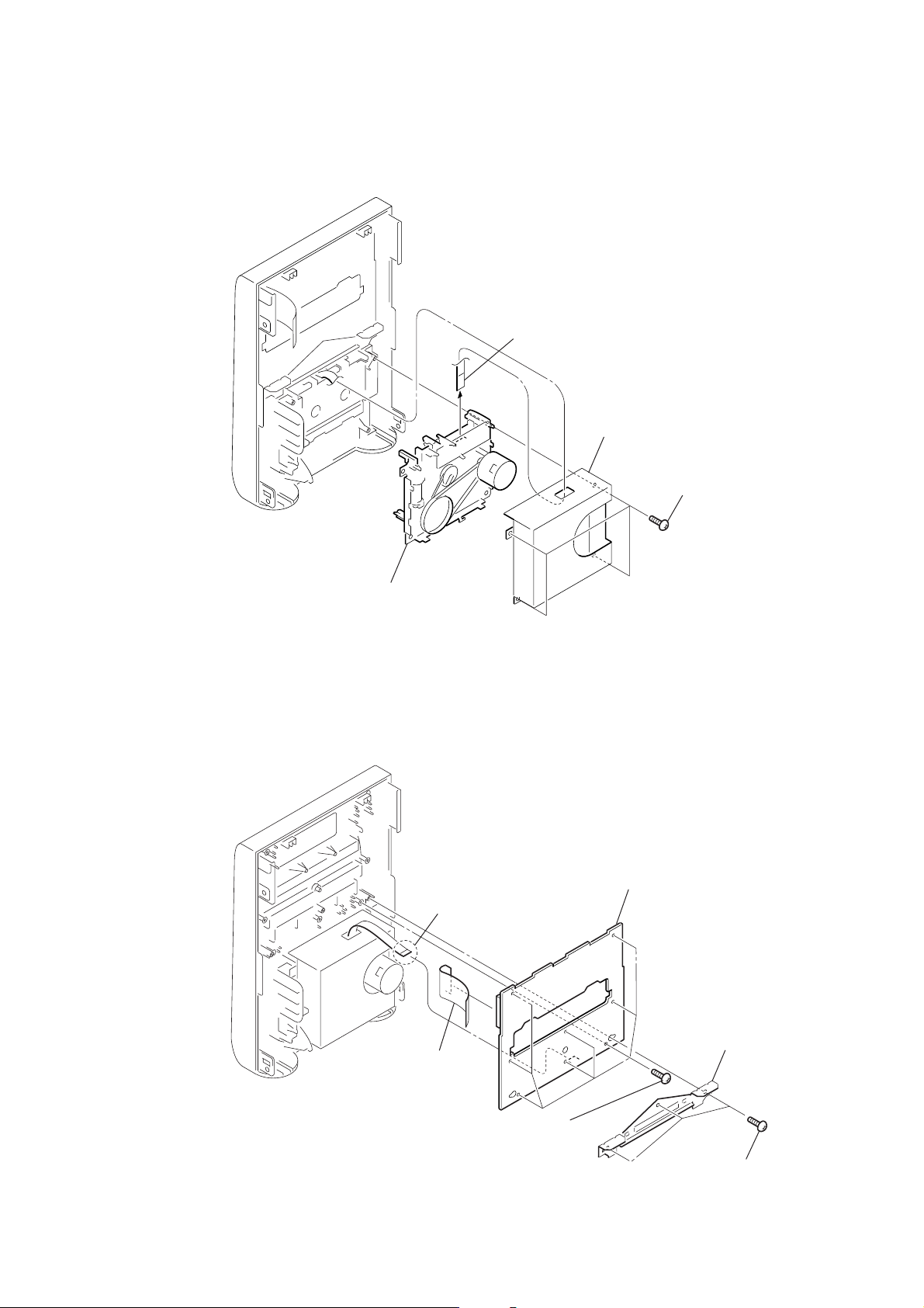
3-6. PANEL (DVD)
3
two
HCD-DV2D
claws
2
4
panel (DVD)
3-7. DVD LOADER (KDA898ST)
1
two s
(+BVTP 3
3
DVD loader (KDA898ST)
crews
× 10
1
screwdriver
2
two s
)
(+BVTP 3
crews
× 10
5
two s
(+BVTP 3
crews
)
×
10)
4
two s
(+BVTP 3
crews
7
holder mecha
× 10
)
6
s
crew
×
(+BVTP 3
10)
11
Page 12
HCD-DV2D
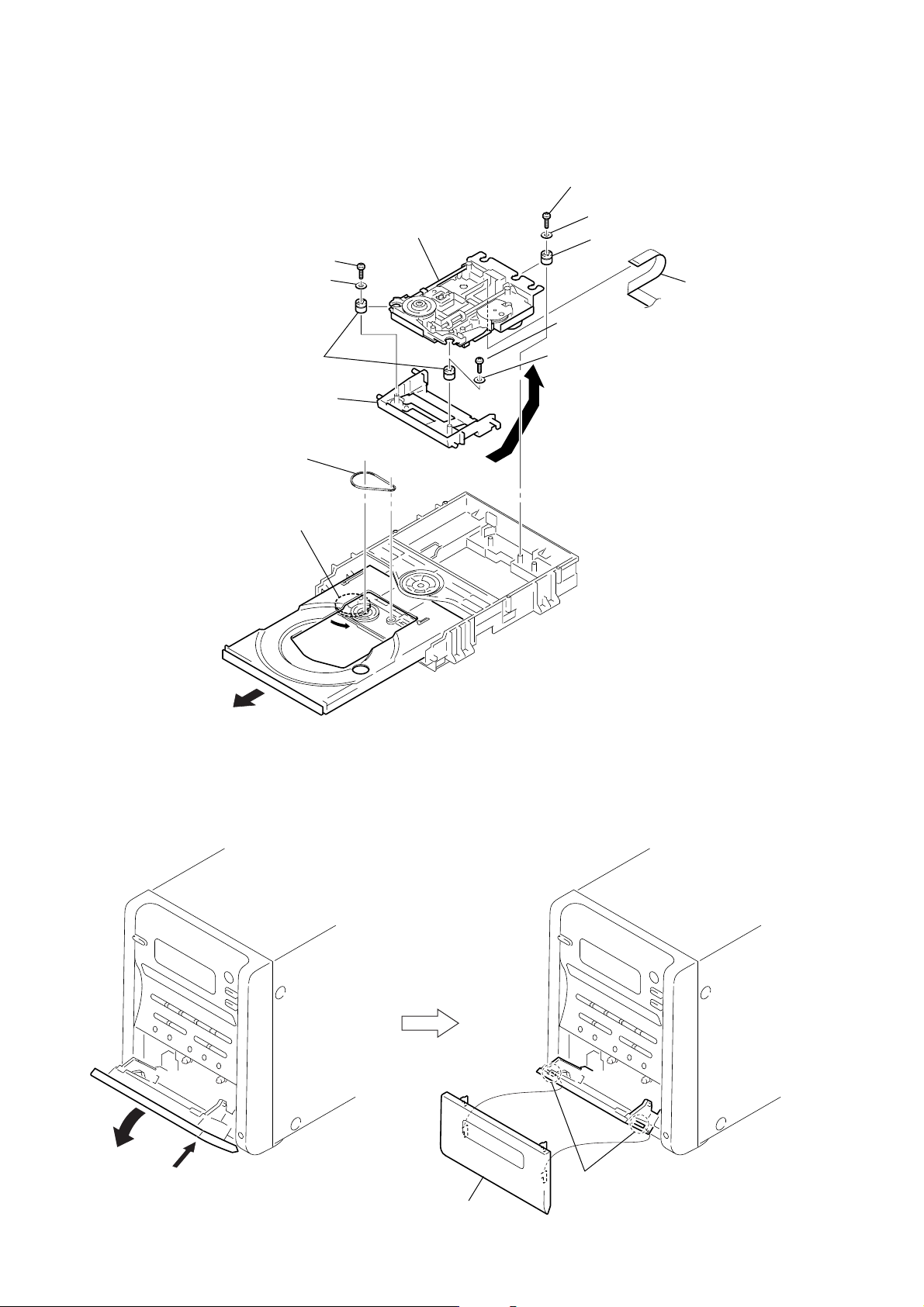
3-8. FRONT PANEL SECTION
3
screw
(+KTP 3
×
8)
6
wire (flat type)
(21core) (CN501)
9
claw
7
connector
(8P) (CN201)
8
claw
5
earth wire
4
screw
(+KTP 3
×
8)
q;
front panel section
3-9. MAIN BOARD
1
two screws
(+BVTP 3
×
10)
2
2
wire (flat type)
(21core) (CN501)
5
(9core) (CN503)
screw
(+KTP 3
wire (flat type)
×
8)
6
wire (flat type)
(11core) (CN203)
7
MAIN board
12
4
connector
(11P) (FW901)
3
connector
(8P) (CN201)
1
two s
(+BVTP 3
crews
×
10)
Page 13
3-10. CASSETTE DECK MECHANISM (CMAL5Z220C)
1
wire (flat type)
(7core)
3
shield cover
2
four screws
(+BVTP 3
×
HCD-DV2D
Ver. 1.2
10)
3-11. KEY BOARD
4
cassette deck mechanism
(CMAL5Z220C)
5
w
ire (flat type)
(21core) (CN601)
4
w
ire (flat type)
(7core) (CN602)
6
KEY board
2
bracket
3
eight screws
(+BVTP 3
×
10)
1
three screws
(+BVTP 3
×
10)
13
Page 14
HCD-DV2D
3-12. TRAVERSE MECH (1ADOMEZ0412)
7
screw
8
washer
qs
two dumpers
(traverse mech)
qg
traverse mech
(1ADOMEZ0412)
9
q;
4
screw
5
washer
qd
dumper (traverse mech)
screw
washer
qf
w
ire (flat type)
24core
3-13. LID TC
qa
holder(traverse mech)
3
belt (pulley)
1
Turn round the gear in the
direction of the arrow.
6
2
14
2
1
4
lid TC
3
two claws
Page 15

SECTION 4
TEST MODE
HCD-DV2D
Note 1:Regarding the notification symbol “R”
Because the number of the operating buttons of this product are
limited, some operations require use of the operating buttons of
the remote commander. When a specific operation requires use
of the operating buttons of the remote commander, “R” is added
to the specific operating procedure in this manual. Example
MENU/NO “R” The MENU/NO button of remote commander .
Note 2:Incorrect operations may be performed if the test mode is not
entered properly.
In this case, press the ?/1 button to turn the power off, and
retry to enter the test mode.
COLD RESET
• The cold reset clears all data including preset data stored in
the RAM to initial conditions. Execute this mode when
returning the set to the customers.
Procedure:
1. Press the ?/1 button to turn the set ON.
2. Press three buttons x , [PLAY MODE] and DVD u simul-
taneously.
3. The message “COLD RESET” is displayed and the set is reset.
TUNER STEP CHANGE
(EXCEPT FOR AEP, UK, RUSSIAN models)
•A step of AM channels can be changed over between 9 kHz
and 10 kHz.
Procedure:
1. Press the ?/1 button to turn the set ON.
2. Select the function “TUNER”, and press [TUNER/BAND]
button to select the BAND “AM”.
3. Press the ?/1 button to turn the set OFF.
4. Press the x and [TUNER/BAND] buttons simultaneously,
and thus the channel step is changed over.
SHIP RESET
Procedure:
1. Press the ?/1 button to turn the set ON.
2. Press the DVD u button to select “DVD”
3. Remove the disc.
4. The message “NO DISC” is displayed.
5. Press three buttons x , [PLAY MODE] and TAPE N si-
multaneously.
6. The message “SHIP RESET” is displayed and the set is reset.
The DVD function is activated.
7. T o exit from this mode, press the ?/1 button and pull out the
AC plug.
PANEL TEST MODE
•This mode is used to check the software version, LCD, LED
and keyboard.
Procedure:
1. Press the ?/1 button to turn the set ON.
2. Press the DVD u button to select “DVD”
3. Press three bottons x , [PRESET EQ] and TAPE N simul-
taneously.
4. When the panel test mode is activated, all segments are turned
on.
VERSION DISPLAY
•This mode is used check the model, destination, software
version.
Procedure:
1. Press the ?/1 button to turn the set ON.
2. Press the DVD u button to select “DVD”
3. Press three buttons x , [PRESET EQ] and [TV] simultaneous-
ly, the model and destination are displayed.
DVD COLOR SYSTEM CHANGE OVER
•The color system can be changed over NTSC or PAL.
Procedure:
1. Press the ?/1 button to turn the set ON.
2. Set the function to “DVD”.
3. Press the ?/1 button to turn the set OFF.
4. Press the x button and ?/1 button simultaneously. The set
will power on automatically.
5. The message “COLOR PAL” or “COLOR NTSC” will be
displayed on the fluorescent indicator tube. The color system
is changed over.
CD Repeat 5 Times Limit Release Mode
Procedure:
1. Press the ?/1 button to turn the set ON.
2. Set the function to “DVD”.
2. Press three buttons x , Z , and DVD u simultaneously.
3. The repeat all mark blinks and then repeat 5 times limit is
released.
DISC TRA Y LOCK
The disc tray lock function for the antitheft of an demonstration
disc in the store is equipped.
Procedure :
1. Press the ?/1 button to turn the set ON.
2. Press the DVD u button to select “DVD”
3. Set disc on the tray, press the x button and the Z button
simultaneously for five seconds.
4. The message “LOCKED” is displayed the tray is locked.
5. To release from this mode, press the x button and the Z
button simultaneously for five seconds again.
6. The message “UNLOCKED” is displayed and the tray is
unlocked.
Note: When “LOCKED” is displayed, the slot lock is not released by
turning power on/off with the ?/1 button.
15
Page 16
HCD-DV2D
DVD SECTION
[GENERAL DESCRIPTION]
The T est Mode allows you to make diagnosis and adjustment easil y
using the remote commander and monitor TV. The instructions,
diagnostic results, etc. are given on the on-screen display (OSD).
[Configuration of Test Mode]
[ SERVICE MODE TEST SEQUENCE ]
RETURN "R"
ENTER "R"
[SYSCON Diagnosis ]
ENTER "R"
RETURN "R"
ENTER "R"
[Version Information ]
"R"
"R"
[MPEG Test]
RETURN "R"
ENTER "R"
[Check DSP]
RETURN "R"
"R"
ENTER "R"
[Check Flash]
RETURN "R"
"R"
ENTER "R"
RETURN "R"
ENTER "R"
[Check SDRAM]
[Check EEPROM]
"R"
ENTER "R"
RETURN "R"
[FRONT PANEL Test]
"R"
RETURN "R"
"R"
ENTER "R"
RETURN "R"
ENTER "R"
[Panel Key Test]
[VFD Test]
RETURN "R"
"R"
ENTER "R"
[Remote Key Test]
RETURN "R"
ENTER "R"
[SERVO Test]
RETURN "R"
1. STARTING TEST MODE
1. Press the ?/1 button to turn the power on, and set the function
to DVD.
2. While pressing the x and Z button at the same time, rotate
the [VOLUME+] knob clockwise to enter the test mode.
3. The message “SERVICE IN” appears on the fluorescent
indicator tube, and the message Test Mode Menu appears on
the monitor screen as follows.
SERVICE MODE TEST SEQUENCE
DVD Service Mode
SYSCON Diagnosis
Version Information
Reset And Exit
1. T o execute each function, press the m “R” or M “R” button
to select the desired menu.Then press the ENTER “R” button.
2. To exit the Test Mode, select the menu “Reset And Exit” and
press the ENTER “R” button.
2. SYSCON Diagnosis
1. Select the menu “SYSCON Diagnosis” and press the
ENTER “R” button.
2. Press the m “R” or M “R” button to select the desired menu.
SYSCON Diagnosis
MPEG T
est
SERVO T
FRONT PANEL
est
Test
3. To exit the Test Mode, press the O RETURN “R” button.
2-1. MPEG Test MENU
1. Select the menu “MPEG Test Menu” and press the
ENTER “R” button.
2. Press the m “R” or M “R” button to select the desired menu.
MPEG Test Menu
16
Check DSP
Check Flash
Check SDRAM
Check EEPROM
3. To exit the Test Mode, press the O RETURN “R” button.
Page 17

HCD-DV2D
2-1-1. Check DSP
1. Select the menu “Check DSP” and press the ENTER “R”
button, then execute this mode.
2. When the check is completed with success, “OK” appears.
When the check finds any failure, “fail” appear.
Check DSP
MCU comm access
Register access
... ok
... ok
3. To exit the Test Mode, press the O RETURN “R” button.
2-1-2. Check Flash
1. Select the menu “Check Flash” and press the ENTER “R”
button, then execute this mode.
2. When the check is completed with success, “OK” appears.
When the check finds any failure, “fail” appears.
Check Flash
2-2. SERVO Test MENU
1. Select the menu “SERVO Test Menu” and press the
ENTER “R” button, then execute this mode.
2. When the check is completed with success, “OK” appears.
When the check finds any failure, “fail” appears.
SERVO Test Menu
Check Motor Driver
... ok
3. To exit the Test Mode, press the O RETURN “R” button.
2-3. FRONT PANEL Test MENU
1. Select the menu “FRONT PANEL Test Menu” and press the
ENTER “R” button, then execute this mode.
2. Press the m “R” or M “R” button to select the desired menu.
FRONT PANEL Test Menu
Status
... ok
3. To exit the Test Mode, press the O RETURN “R” button.
2-1-3. Check SDRAM
1. Select the menu “Check SDRAM” and press the ENTER “R”
button, then execute this mode.
2. If error is detected, the “ Address” and the “Error” count appear.
Check SDRAM
Address
Error
X x XXXX
X
3. To exit the Test Mode, press the O RETURN “R” button.
2-1-4. Check EEPROM
1. Select the menu “Check EEPROM” and press the
ENTER “R” button, then execute this mode.
2. If error is detected, the “ Address” and the “Error” count appear.
Panel Key Test
VFD Test
Remote Key Test
3. To exit the Test Mode, press the O RETURN “R” button.
2-3-1. Panel Key Test
1. Select the menu “PANEL KEY Test” and press the
ENTER “R” button, then execute this mode.
2. Press TAPE N , x , M > , .m button on the
Front panel in this order.
3. When the check is completed with success, “OK” appears.
When the check finds any failure, “fail” appears.
Panel Key Test
... ok
PLAY
Stop
Next
Prev
... ok
... ok
... ok
4. To exit the Test Mode, press the O RETURN “R” button.
Check EEPROM
Address
Error
X x X X
X
3. To exit the Test Mode, press the O RETURN “R” button.
17
Page 18
HCD-DV2D
2-3-2. VFD T est MENU
1. Select the menu “VDF T est Menu” and press the ENTER “R”
button, then execute this mode.
2. When the check is completed with success, “OK” appears.
When the check finds any failure, “fail” appears..
VFD Test
... ok
Status
3. To exit the Test Mode, press the O RETURN “R” button.
2-3-3. IR Remote Test
1. Select the menu “IR Remote T est” and press the ENTER “R”
button, then execute this mode.
2. Press TAPE N , x , > , . button on the remote
commander in this order.
3. When the check is completed with success, “OK” appears.
When the check finds any failure, “FAIL” appears.
IR Remote Test
... ok
PLAY
Stop
Next
Prev
... ok
... ok
... ok
4. To exit the Test Mode, press the O RETURN “R” button.
3. Version Information
1. Select the menu “Version Information” and press the
ENTER “R” button, then execute this mode.
2. The “Version” appears.
Version Information
MPEG Version
: XXX.XX.XX.XX.X
3. To exit the Test Mode, press the O RETURN “R” button.
18
Page 19
SECTION 5
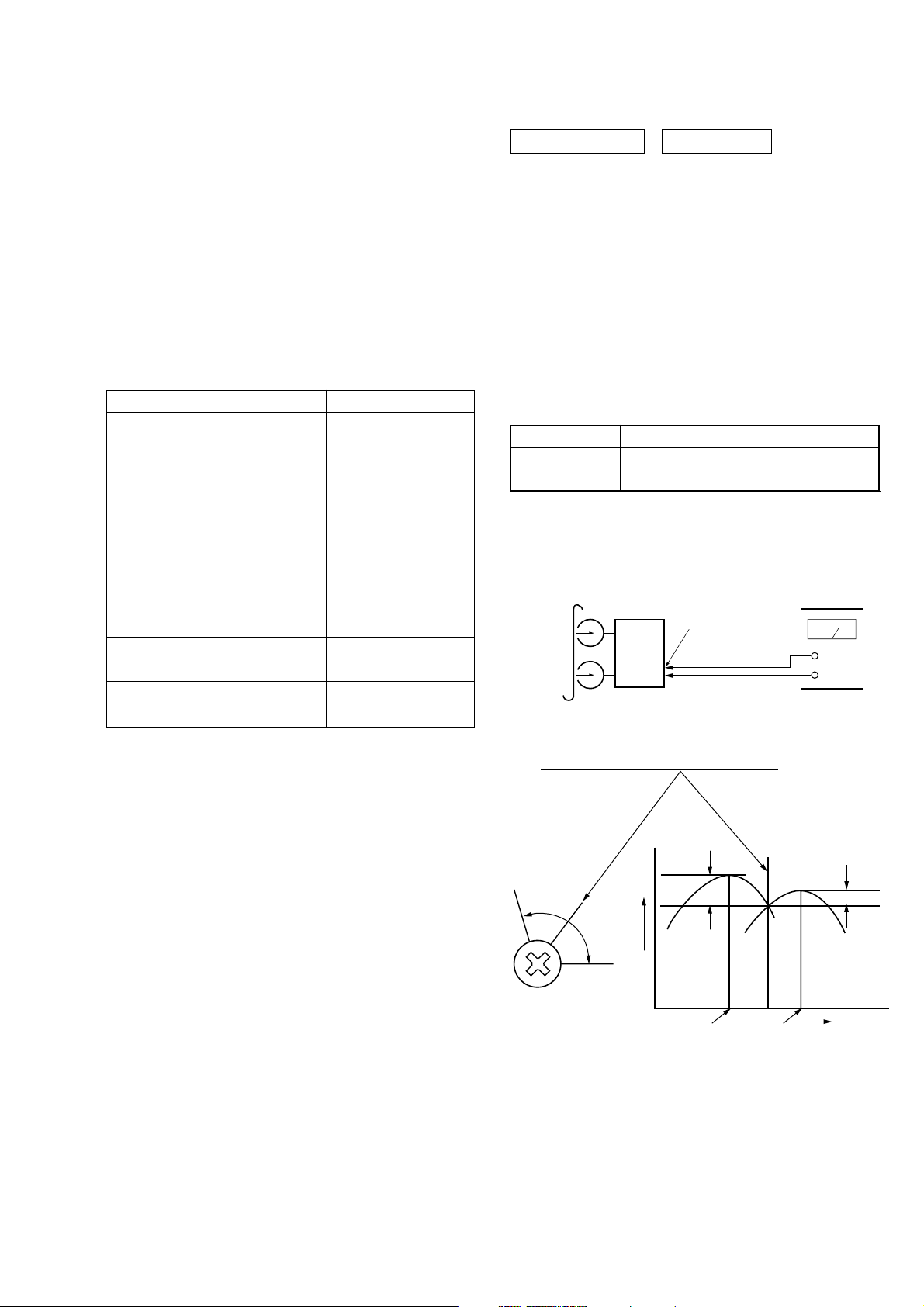
test tape
P-4-A100
(10kHz, –10dB)
MAIN board
JK102
speaker terminal
level meter
set
+
–
MECHANICAL ADJUSTMENTS
HCD-DV2D
SECTION 6
ELECTRICAL ADJUSTMENTS
Precaution
1. Clean the following parts with a denatured alcohol-moistened
swab:
record/playback heads pinch rollers
erase head rubber belts
capstan idlers
2. Demagnetize the record/playback head with a head demagnetizer.
3. Do not use a magnetized screwdriver for the adjustments.
4. After the adjustments, apply suitable locking compound to
the parts adjusted.
5. The adjustments should be performed with the rated power
supply voltage unless otherwise noted.
Torque Measurement
Mode
FWD
FWD
back tension
REV
REV
back tension
FF/REW
FWD tension
REV tension
Torque meter Meter reading
2.94 – 7.84 mN • m
CQ-102C
CQ-102C
CQ-102RC
CQ-102RC
CQ-201B
CQ-403A
CQ-403R
(31 to 71 g • cm)
(0.43 – 0.98 oz • inch)
0.15 – 0.59 mN • m
(2 to 6 g • cm)
(0.02 – 0.08 oz • inch)
2.94 – 7.84 mN • m
(30 to 79 g • cm)
(0.42 – 1.11 oz • inch)
0.15 – 0.59 mN • m
(2 to 6 g • cm)
(0.03 – 0.08 oz • inch)
6.86 – 17.64 mN • m
(71 to 143 g • cm)
(0.98 – 2.49 oz • inch)
9.8 mN • m or more
(100 g • cm or more)
(1.4 oz • inch or more)
9.8 mN • m or more
(100 g • cm or more)
(1.4 oz • inch or more)
DECK SECTION 0 dB=0.775V
1. Demagnetize the record/playback head with a head
demagnetizer.
2. Do not use a magnetized screwdriver for the adjustments.
3. After the adjustments, apply suitable locking compound to
the parts adjusted.
4. The adjustments should be performed with the rated power
supply voltage unless otherwise noted.
5. The adjustments should be performed in the order given in
this service manual. (As a general rule, playback circuit
adjustment should be completed before performing recording
circuit adjustment.)
6. The adjustments should be performed for both L-CH and RCH.
7. Switches and controls should be set as follows unless otherwise
specified.
Signal Used forTape
P-4-A100
WS-48B
[Record/Playback Head Azimuth Adjustment]
Procedure:
1. Mode : Playback
2. Turn the adjustment screw and check output peaks. If the peaks
do not match for L-CH and R-CH, turn the adjustment screw
so that outputs match within 1 dB of peak.
10 kHz, –10 dB
3 kHz, 0 dB
Azimuth Adjustment
Tape Speed Adjustment
L-CH
peak
screw
position
R-CH
peak
output
level
within
1 dB
L-CH
peak
R-CH
peak
within 1dB
screw
position
19
Page 20
HCD-DV2D
+
–
MPEG board
oscilloscope
TP (RF)
TP (VC)
3. Mode: Playback
test tape
P-4-A100
(10kHz, –10dB)
set
in phase 45
MAIN board
JK102
speaker terminal
L
R
Waveform of oscilloscope
°
90
°
good
135
oscilloscope
°
wrong
180
°
4. After the adjustments, apply suitable locking compound to
the parts adjusted.
Adjustment Location: Record/Playback/Erase Head
DVD SECTION
[RF Level Check]
Check the RF level when optical pick-up block (TRAVERSE
MECH) is replaced.
Connection:
Procedure:
1. Connect an oscilloscope to TP (RF) and TP (VC) on the MPEG
board.
2. Turn the power on.
3. Set the test disc on the tray and press DVDu button to
playback.
4. Observe the waveform of the oscilloscope, and check that the
RF level is satisfied to specified value.
[Test Disc List and Specified Value]
Use the following test disc on adjustment.
TEST DISC Specified Value Deviation
CD (YEDS-18)
PART No. :3-702-101-01
DVD Single Layer (HLX-504)
PART No. :J-6090-088-A
DVD Dual Layer (HLX-505)
PART No. :J-6090-089-A
310 mV +30 mV/–50 mV
290 mV +25 mV/–40 mV
120 mV +20 mV/–30 mV
adjustment screw
Note: Refer to “ 3-13. LID TC ” (see page 14)
[Tape Speed Check]
Procedure:
1. Turn the power on.
2. Insert the WS-48B into deck.
3. Press the TAPE N button of deck.
4. Check the reading of frequency counter becomes 3000 ± 90
Hz.
Note: Do not use existing test disc for DVD.
Checking Location: MPEG board
[MPEG BOARD]
U709
TP (RF) TP (VC)
Sample Value of Wow and flutter
W.RMS (JIS) less than 0.3%
(test tape: WS-48B)
20
Page 21
SECTION 7
DIAGRAMS
HCD-DV2D
Ver. 1.2
THIS NOTE IS COMMON FOR PRINTED WIRING BOARDS AND SCHEMATIC DIAGRAMS.
(In addition to this, the necessary note is printed in each block.)
For Schematic Diagrams.
Note:
• All capacitors are in µF unless otherwise noted. (p: pF)
50 WV or less are not indicated except f or electrolytics and
tantalums.
• All resistors are in Ω and 1/
specified.
• f : internal component.
• C : panel designation.
Note:
The components identified by mark 0 or dotted line with mark 0 are
critical for safety.
Replace only with part
number specified.
• A : B+ Line.
•Voltages and waveforms are dc with respect to ground
under no-signal (detuned) conditions.
– MPEG Section –
No mark: DVD STOP
– Other Section –
No mark: FM
< > : T APE REC
•Voltages are taken with a VOM (Input impedance 10 MΩ).
Voltage variations may be noted due to normal production
tolerances.
•Waveforms are taken with a oscilloscope.
Voltage variations may be noted due to normal production
tolerances.
• Circled numbers refer to waveforms.
• Signal path.
F : AUDIO
d : TUNER
E : PB(TAPE)
a : REC(TAPE)
J : DVD (AUDIO)
c : DVD (RF)
I : DVD (DIGITAL)
h : TV IN
L : VIDEO
q : R,G,B
•Abbreviation
AUS: Australian model.
CND : Canadian model.
E2 : 120 V AC area in E model.
E3 : 240 V AC area in E model.
E51 : Chilean and Peruvian model.
KR : Korea model.
RU : Russian model.
SP : Singapore model.
TW : Taiwan model.
4
W or less unless otherwise
Note:
Les composants identifiés
par une marque 0 sont critiques pour la sécurité.
Ne les remplacer que par une
piéce portant le numéro
spécifié.
For Printed Wiring Boards.
Note:
• X : parts extracted from the component side.
• Y : parts extracted from the conductor side.
• f : internal component.
• : Pattern from the side which enables seeing.
Caution:
Pattern face side: P arts on the pattern face side seen from
(Side A) the pattern face are indicated.
Parts face side: Parts on the parts face side seen from
(Side B) the parts face are indicated.
• Indication of transistor.
C
Q
B
B
B
E
CE
Q
CE
These are omitted.
These are omitted.
These are omitted.
• Circuit Boards Location
AV board (EXCEPT AEP, UK, RU)
AV board (AEP, UK, RU)
MAIN board
KEY board
MPEG board
POWER board
AMP board
HCD-DV2D
HP board
2121
Page 22
HCD-DV2D
7-1. BLOCK DIAGRAMS — MPEG-1 SECTION —
OPTICAL
PICK-UP
CD/DVD
VR-CD
VR-DVD
MD
LD-DVD
LD-CD
F-
F+
T+
T-
A
B
C
D
E
F
F-
F+
T+
T-
VR CONTROLLER
VR CONTROLLER
Q710
CD/DVD
SELECTOR
Q711,712
(CD)
Q713
(DVD)
Q714
POWER
CONTROLLER
(DVD)
Q715
POWER
CONTROLLER
(CD)
RFN
55
CAP
1
CAO
62
PD2
5
PD1
4
PD4
7
PD3
6
TIN2
14
TIN1
13
FIN1
9
FIN2
10
DVD/CD
26
DPD/TE
27
LDS1
16
LDS2
18
LDD1
15
LDD2
17
U709
RF AMP
FOCUS/TRACKING
ERROR AMP
59
PFP
55
61
RFOP
RFON
LDON2
LDON1
RREC
WO
LDON1
LDON2
XHTR
RST
TEBL
FEBL
SGC
DVD/CD
DVD/TE
55
54
22
21
38
PH
47
BH
46
TE
40
FE
39
41
21
22
31
FC
34
33
TH
30
36
CP
37
35
32
26
27
GU
25
EFNINP
10
EFNINN
12
LDON2
172
LDON1
171
PREC
4
RFPH
5
RFBH
6
BHC
19
TE
7
TEC
21
FE
8
WO
20
LDON1
171
LDON2
172
XHTR
170
FO
25
RST
26
DEFECTO
168
TBAL
27
FBAL
28
SGC
29
TSTD1
23
TSTDO
24
DVD CD
167
AD11VREF22AD02SLCO30SPDO31TDO
XIN
134
XOUT
135
145-148
MD8-15
150-153
156-159
MD0-7
161-164
MWEB
60
MRAS1B
61
62-65
MA0-8
68-72
MCASUB
77
U707
AV DECODER
SERVO CONTROLLER
HOST INTERFACE
HDAT1-7
HADR0-12
54-59,78-83
FG (PP1)
HIROB37HWAITB38HRESB39HRDB40HWRD41HCSB42HDATO
36
SDO
32
33
46-53
MA10
MOEB
AVD0-7
DO0T
AVERRB
AVSCTB
AVDACK
AVACKO
AVRAOI
LRSY
ROMCK
ROMXA
C2F
X16MIO
75
76
96
-
103
142
95
94
93
92
91
87
86
85
84
137
43
16.9344MHz
DFFR
DBGN
DCLK
DACK
DRFO
LRCK
BCK
CD DATA
C2F
AMCLK
Y701
31-34,
36-39
2-5,
7-10
13
14
16-19
22-26
29
27
28
WE
RAS
A0-8
CASL
OE
CASH
DO0T
U708
S-RAM
IO8-15
IO0-7
H
E
MPEG2
SECTION
MPEG2
SECTION
OPEN SW
CLOSE SW
MLD2
MLD1
SLED+
SLED-
PANEL POWER
SECTION
PANEL POWER
SECTION
HCD-DV2D
SP+
SP-
SPD FG
INT DEC
RDY
LSI RSTRDWR
HA0-12
HA0-7
DATA&ADDRESS BUS
F-
F+
T+
TOP
TCL
D
C
T-
U705(1/2)
AMP
2
1
3
OPN
CLS
VOL3+
8
VOL3-
9
VOL4+
7
VOL4-
6
VOL0+
5
VOL0-
4
VOL1-
13
VOL1+
12
VOL2+
10
VOL2-
11
FWD
1
REW
2
U706
MOTOR
DRIVER
VIN4+
VREF-IN
VIN3+
VIN2+
VIN1+B
VIN1+A
VIN1-B
VIN2-
VIN4-
VIN3-
31
30
25
22
19
17
18
21
32
24
U705(2/2)
5
6
AMP
7
SC DVD
BE01
• Signal Path
MPEG2
I
SECTION
MPEG2
J
SECTION
MPEG2
G
SECTION
: DVD(RF)
: DVD(DIGITAL)
2222
Page 23
— MPEG-2 SECTION —
MPEG1
J
SECTION
DATA& ADDRESS BUS
WE12RST
11 28
HCD-DV2D
AEP,UK,RU
R
G
B
VOUT
UD707
FLASH MEMORY
A0
4-8,
18-25
A12
DO0
29,31,33,35,
38,40,42,44
DO7
DO8
30,32,34,36,
39,41,43,45
DO14
OE
A13
3-1,48,
17,16,9
A19
UD708
EEPROM
SDA
5 6
SCL
B
R
G
JK803
15
11
7
19
16
8
R
G
B
VOUT
BLAK
SW
–LINE–TV
PANEL POWER
SECTION
MPEG1
SECTION
MPEG1
SECTION
MPEG1
SECTION
HA0-12
MRST
RD
WR
BEO1
SCDVD
154,155
MEMAD13
RAMADD11
68
MEMAD19
RAMBA0
115,118,120,
122,106,108,
110,112
MEMDA8
MEMDA15
RAMBA166PCLK78RASWE75RASCAS74RAMRAS72RADOM
123
MEMRD
MFWOS2
53-55,57-60,
62-64,67
147-150,152
RAMADD0
105
129
128
MEMWR
F
DSSTB
DSCK
DSDA
G
H
I
DRFO
DACK
DFFR
DBGN
DCLK
C2F
LRCK
BCK
CD DATA
AMCLK
SPD FG
RDY
INTDET
LSI RST
7
SSCRRO/CPCIO11
8
SSCRRO/CPCIO10
49
SSCRXD/GPCI08
51
SSCRXD/GPCI09
34
ATDA2
9
14
ATDD4-11
16
18
ATDD11
19
ATDD13
20
ATDD12
21
ATDD2
22
ATDD1
23
ATDA1
36
ATDA0
37
ATCS1
38
ATCS0
39
AMCLK
179
GPCI07
47
ATIORD
31
GPCIO1
41
GPCIO14
4
MEMDAO
HA0-12
131,133-138
140,142-146
MEMAD0
MEMAD12
UD705
VIDEO DAC ENCODER
76
HA0-7
HA0-7
105,107,109,
111,113,
117,119,121
MEMDA0
MEMDA7
RAMDAT0-15
80,82,84,86,87,89,
90,92,93,95,96,98,
99,101,102,104
196
195
GCLKP
CPCIO16
CPCIO17
CVBS/C
CVBS/C/Y
C/B/V
ICE TCK
ALR CLK
AOUT O
AMCLK
JTMS/CPCIO47
GPC106
GPC105
Q856
VOUT
XO
160
161
162GCLKA
170
169
172V/R/Y
173
198
194LLCFGP
193LLCFGA
177GPCIO18
181SPDIF/AOUT3
190AB CLK
188
184
179
203
46
45
YD701
27MHz
VIDEO1
G
R
B
QD707,710
BLANKOUT CONTROL
QD706
BLANKOUT CONTROL
QD705
SWITCH
16
15
14
13
SCK
ML
MC
MD
2
DATA3LRCK
U704
AUDIO DAC
FS1
FS2
1
BCK
VOUTL
VOUTR
VOUT
UD701
BUFFER
SEL
2
VIN2
3
MPEG1
SECTION
7
8
R-CH
DOUT
E
VOUT
VIN1
1
UD709
2 1
BUFFER
7
SW
CONTROL
EXCEPT AEP,UK,RU
JK101
TX
AUDIO
SECTION
B
DIGITAL OUT
OPTICAL
JK1
Q851,855
BLANKOUT
SWITCH
VIDEO OUT
• R-CH is omitted due to same as L-CH.
• Signal Path
: DVD(AUDIO)
: DVD(RF)
: DVD(DIGITAL)
: VIDEO
: R,G,B
HCD-DV2D
20-24,
27-32
A0-A10
19
18 35 15 16 17 14 36
CS
WE
A11
CLK
CAS
UD706
DRAM
RAS
LDOM
UDOM
2,3,5,6,8,9,11,
12,39,40,42,43,
45,46,48,49
D0-D15
2323
Page 24

HCD-DV2D
— AUDIO SECTION —
TV IN
FM 75Ω
COAXIAL
ANTENNA
AM
JK201
L
R
TUNER PACK
L-CH
R-CH
D OUT
D IN
CL
CE
TUNED
MUTE
STEREO
RDDA
ROCK
R-CH
R-CH
IC501(1/2)
SYSTEM CONTROLLER
TUDO
19
TUDI
18
TUCK
20
TUCE
12
TUND
13
RMUTE
1
STE
11
RDDA
21
RDCK
46
RMUT
2
RPHD
3
BIAS
4
MPEG2
SECTION
SDAT/ROMDA
SCK/ROM CK
AMUTE
TSOL
TMOT
TCNT
REPT
HDPN
IC102
MIXER AMP
B
53
54
59
5
6
7
31
30
1
2
3
IC101
SOUND PROCESSOR
LOUT
VARL
6
IN4
28
LINT2
30
LINT3
29
LINT1
31
BASSOL
7
SDA
21
RECOUTL
SCL
22
SCL
6
SDA
5
Q105
MUTE CONT
25
27
IC503
EPROM
Q102
MUTE
A
PANEL
POWER
SECTION
R-CH
Q319
MUTE
SWITCH
Q314,317
CURRENT
DETECT
IC103
POWER AMP
CH1
IN
STBY
INVERTER
OUT+
Q199
CH1
11 4
13
Q308
PROTECT
SWITCH
Q104,301
OVER LOAD
DETECT
R-CH
Q303,304,354
DC PROTECT
R-CH
R-CH
R-CH
Q350-352
FAN CONT
L
R
JK103
PHONES
JK102
SPEAKER
IMPEDANCE
USE 6Ω
FAN
TAPE
MECHANISM
DECK
L-CH
REC/PB
HEAD
R-CH
ERASE
PACK
RECF
RECR
HDPLY
TCNT
MOT
R-CH
R-CH
Q209
MUTE
Q653,654
MOTOR DRIVER
Q202,207
REC/PB SWITCH
Q201,204,206
REC/PB SWITCH
Q212
Q213
BIAS
USC
+VM
Q214
IC201
TAPE REC/PB AMP
CH I/A
1
PREO
REC IN
RECO
14
3
16
16
Q215
REC DETECT
Q210
MUTE
+10V +VDD
Q313
+10V REG
• R-CH is omitted due to same as L-CH.
• Signal Path
: AUDIO
: PB(TAPE)
: REC(TAPE)
: TUNER
: DVD(AUDIO)
: TV IN
Q353,355
FAN CURRENT
DETECT
HCD-DV2D
SOL
Q651,652
SOL DRIVER
2424
Page 25

— PANEL/POWER SECTION —
TRANSFORMER(MAIN)
VF
VF
PT901
POWER
HCD-DV2D
Ver. 1.1
S658,S651-654
FUNCTION
KEY
S665,S666,S656,S657,S659
FUNCTION
KEY
S655,S660-664
FUNCTION
KEY
REMOTE
CONTROL
RECEIVER
IR651
1
32.768kHz
X501
X502
8.38MHz
IC501 (2/2)
SYSTEM CONTROLLER
KEY1
26
KEY2
27
KEY3
28
REM
45
37
XT2
38
XT1
40
X2
41
X1
VFSTB
VFCK
VEDA
LED
PCON
INH
TUON
CD ON
-33V(VPP)
Q306
SWITCH
IC651
FL DRIVER
GRID1-4
I/
14-29,
31-38
42-39
30
-33V(VPP)VEE
17
16
15
Q502
LED
60
DRIVE
64
44
61
62
SEG1-SEG24
9
STB
8
CLK
7
DIN
D652
VFD651
FLUORESCENT
INDICATOR
TUBE
AUDIO
VF
VF
SECTION
+9V (TU)
Q196,197
SWITCH
A
Q318
SWITCH
Q305,Q320
POWER
CONTROL
Q309,310
SWITCH
Q198
+9V
REG
D309
D324
D +5V
+12V(VM)
+9V
+1.8V
+3.3V
+2.5
+3.3V
Q315
-33V
REG
POWER AMP B+
POWER AMP B-
+VDD
IC301
+5V
2
REG
5
Q311,312
+12V
REG
Q316
+9V
REG
UD703
+1.8V
3
REG
UD702
+3.3V
3
REG
UD704
+2.5V
REG
U702
+3.3V
REG
D306
D301
D302
1
1
1
12
12
D+5V
MPEG1
SECTION
MPEG1
SECTION
MPEG2
SECTION
HCD-DV2D
RY901
C
D
F
CLS
OPN
TOP
TCL
DSCK
DSSTB
DSDA
MRST
CLS
56
OPN
55
14
TOP
35
TCL
DSCK
50
DSSTB
49
DSDA
48
MRST
47
RLY
FPON
RST
AVR
SFTY
63
Q504-506
+5V
REG
+12V(VM)
D501
D901-904
Q507
SWITCH
22
IC502
RESET
36
SWITCH
34
29
+5V
D906
Q307
RELAY
DRIVE
TRANSFORMER
D907
PT902
POWER
(SUB)
E2,E3,E51,SP
SW901
VOLTAGE
SELECTOR
EXCEPT E2,E3,E51,SP
AC IN
2525
Page 26

HCD-DV2D
Ver. 1.2
7-2. PRINTED WIRING BOARD — MAIN SECTION-1 —
• See page 21 for Circuit Boards Location. :Uses unleaded solder.
A
B
C
D
E
F
12
MAIN BOARD
L
TV
IN
R
+
L
–
SPEAKER
IMPEDANCE USE 6Ω
–
R
+
345678910
TUNER
PACK
C
MPEG BOARD
J702
(Page 29)
B
MPEG BOARD
J701
(Page 29)
DOWN LOAD PORT
A
KEY BOARD
CN601
(Page 32)
HEAD
(PLAYBACK/ERASE)
L-CH
REC/PB
HEAD
R-CH
ERASE
HEAD
IC201
• Semiconductor
Location
Ref. No.
D105 G-2
D196 B-2
D197 B-3
D198 B-3
D199 B-3
D201 E-7
D301 I-6
D302 I-8
D306 I-8
D307 I-9
D308 I-8
D310 H-9
D312 G-2
D314 H-2
D317 G-2
D319 G-4
D320 F-4
D321 F-4
D322 F-4
D323 H-5
D401 H-7
D501 E-9
D502 C-9
D503 D-8
D505 D-8
D507 G-6
D508 H-8
IC201 E-8
IC301 H-6
Location
HCD-DV2D
G
H
K
Q198 B-3
Q212 F-9
Q213 F-9
Q214 F-9
Q215 D-8
H
AMP BOARD
CN108
(Page 36)
Q313 G-3
Q315 I-9
Q316 H-8
Q504 C-8
IC301
E
AMP BOARD
CN106
I
J
(Page 36)
I
AMP BOARD
CN102
(Page 36)
POWER BOARD
D
FW901
(Page 36):
(E2,E3,E51,SP,TW MODELS)
(US,CND MODELS)
(SUPPLEMENT-1:Page 3):
(AEP,UK,RU,KR,AUS MODELS)
2626
Page 27

HCD-DV2D
7-3. PRINTED WIRING BOARD — MAIN SECTION-2 —
12
A
MAIN BOARD
B
C
D
E
F
• See page 21 for Circuit Boards Location. :Uses unleaded solder.
345678
IC501
IC502
IC503
IC101
IC102
• Semiconductor
Location
Ref. No.
D106 C-8
D107 C-8
D309 I-3
D313 G-4
IC101 D-5
IC102 E-5
IC501 B-3
IC502 C-2
IC503 C-3
Q196 B-7
Q197 B-7
Q199 B-7
Q201 F-3
Q202 D-3
Q203 F-3
Q204 F-3
Q205 F-3
Q206 E-4
Q207 E-4
Q208 D-3
Q209 D-3
Q210 D-2
Q211 E-2
Q305 I-3
Q306 I-1
Q307 H-2
Q317 G-4
Q318 G-4
Q319 I-2
Q502 B-2
Q505 C-2
Q506 C-2
Q507 B-2
Location
G
H
I
HCD-DV2D
2727
Page 28

HCD-DV2D
Ver. 1.2
7-4. SCHEMATIC DIAGRAM — MAIN SECTION —
TO TUNER PACK
• See page 41, 42 for IC Block Diagrams. • See page 40 for Waveforms. • See page 45 for IC Pin Function Description.
TV IN
A
(Page 33)
DOWNLOAD
PORT
B
(Page 31)
HEAD
(PLAYBACK/ERASE)
L-CH
REC/PB
HEAD
R-CH
ERASE
HEAD
KEY
BOARD
CN601
MPEG
BOARD
J701
MAIN BOARD
4.9
4.9
SWITCH
4.2
Q201-Q205
REC/PB SWITCH
2.6<-7.0>
0<-14.9>
2.6
<-7.0>
2.6
<-7.0>
2.9
2.9<-11.1>
<0>
REC/PB SWITCH
Q212, Q213
BIAS OSC
∗∗
R581
0<0>
0<0>
0<-0.7>
0<0>
0<-14.9>
0<0>
0<-0.7>
0<0>
0<-14.9>
2.9
2.9
<0>
<-0.7>
REC/PB SWITCH
9.6
9.5
<9.0>
<2.3>
9.6<2.7>
9.6<2.2>
9.6
<9.0>
1.2k:AEP,UK
2.7k:SP,KR,TW
4.7k:US,CND,E2,E51
10k:RU
24k:AUS,E3
AEP, UK, RU Model
SYSTEM CONTROLLER
5.0
5.0
IC502
RESET SWITCH
0
1.2
2.0
1.4
7.1
2.0
1.2
3
VOLTAGE CHART
IC501
NO.
VOLT
1
9.5 <0.4>
0<0.8>
4.9
2
4.9
3
4.9
4
0
5
0
6
0
7
0
8
0
9
–
10
5.0
11
0
12
0
13
0
14
4.8
15
0
16
0
0
INVERTER
4.9
IC501
12
IC B/D
0
NO.
17
18
19
20
21
22
23
24
25
26
27
28
29
30
31
32
0
IC201
TAPE REC/PB AMP
MUTE
0.7
VOLT
4.9
0
0.3
0
0.2
4.9
0.2
5.1
–
5.0
5.0
5.0
2.8
3.8
3.8
0.4
0.3
+9V REG
12.4
0
12.4
0
SWITCH
12.3
12.4
AMP BOARD
CN108(Page 37)
H
5.0
Q504-506
LED DRIVE
0
0.3
4.9
5.0
4.9
EPROM
IC503
Q210, Q211
0
1.2
2.2
1.7
1.7 <0.8>
2.3
0
1.2
00
0
Q215
REC DETECT
0.7
MUTE
0
NO.
VOLT
NO.
33
4.9
49
34
5.0
50
35
0
51
36
5.0
52
37
3.3
53
38
2.4
54
39
0
55
40
3.0
56
41
2.8
57
42
–
58
43
0
59
44
4.9
60
45
4.9
61
46
0
62
47
4.9
63
48
3.2
64
VOLT
0
0.7
<0>
0
3.4
4.8
0.3
0
4.9
4.9
0
0
4.9
0
4.9
0
0
4.9
4.9
4.9
11.3
0.7<0>
0.6
+5V REG
5.7
0.7
0
0.7
0.2
10.6
10.3
MUTE
0
0
C
MPEG BOARD J702
(Page 31)
5.0
5.0
0
5.0
5.0
5.0
0
IC101
SOUND PROCESSOR
IC B/D
IC301
+5V REG
4.3
4.3
4.3
4.3
4.9
4.9
2.6
0
SWITCH
MUTE SWITCH
4.9
POWER
0
CONTROL
0.6
0
0.6
0
POWER
CONTROL
9.9
11.0
+10V REG
16.3
18.0
CURRENT
DETECT
17.8
0
17.0
+9V REG
8.8
10.8
5.0
5.0
5.0
5.0
5.0
IC102
MIXER AMP
9.9
5.0
5.1
5.1
17.8
0
0
0.7
SWITCH
AMP BOARD
I
CN102(Page 37)
-32.9
-32.4
-33V REG
-38.6
E
AMP BOARD
CN106
(Page 37)
+
L
SPEAKER
–
IMPEDANCE
–
USE 6Ω
R
+
D
POWER BOARD
FW901
(Page 38):
E2, E3, E51, SP, TW MODEL
(Page 39):
US,CND MODEL
(SUPPLEMENT-1:Page 4):
AEP,UK,RU,KR,AUS MODEL
RELAY DRIVE
0
4.5
NO MARK : FM
< > :TAPE REC
HCD-DV2D
2828
Page 29

7-5. PRINTED WIRING BOARD — MPEG SECTION-1 —
HCD-DV2D
Ver. 1.2
• See page 21 for Circuit Boards Location. :Uses unleaded solder.
12
A
MPEG BOARD
34567891011121314
(SIDE A)
MONITOR DEBUGGER DEBUG TERMINAL
• Semiconductor
Location
Ref. No.
B
UD701
U704
UD708
EXCEPT AEP,UK,RU
F
AV BOARD
CN851A
(Page 34)
J
AV
BOARD
CN851B
(Page 34)
AEP,UK,RU
C
U707
D
UD706
UD705
U708
E
D701 G-2
D702 G-6
D703 G-7
D704 I-13
D705 J-8
D706 C-12
DD702 H-10
DD703 H-10
DD705 F-13
DD706 F-12
DD707 E-13
DD708 E-12
DD709 F-13
DD710 F-6
DD711 F-6
DD712 F-6
Q710 G-6
Q711 G-6
Q712 G-6
Q713 G-7
Q714 G-5
Q715 G-5
QD705 D-12
Location
F
G
H
U702 J-8
U704 D-11
U705 H-2
UD707
UD703
UD704
U705
U709
I
U706
UD702
UD709
U706 I-3
U707 D-4
U708 D-2
U709 H-5
UD701 B-12
UD702 I-10
UD703 G-9
UD704 G-8
UD705 D-9
UD706 D-6
UD707 F-8
UD708 C-11
UD709 H-12
U702
J
HCD-DV2D
K
DVD
MECHANISM
BLOCK
DVD
MECHANISM
BLOCK
DVD
MECHANISM
BLOCK
MAIN
B
BOARD
CN503
(Page 26)
C
MAIN
BOARD
CN302
(Page 26)
2929
Page 30

HCD-DV2D
7-6. PRINTED WIRING BOARD — MPEG SECTION-2 —
12
A
MPEG BOARD
34567891011121314
(SIDE B)
B
C
D
• See page 21 for Circuit Boards Location. :Uses unleaded solder.
• Semiconductor
Location
Ref. No.
QD706 D-2
QD707 D-3
QD710 D-2
Location
G
H
E
F
I
J
K
HCD-DV2D
3030
Page 31

7-7. SCHEMATIC DIAGRAM — MPEG SECTION —
HCD-DV2D
Ver. 1.2
• See page 42, 43 and 44 for IC Block Diagrams. • See page 40 for Waveforms. • See page 47, 51 for IC Pin Function Description.
CD738 0.1
AEP,UK,RU
AV
BOARD
CN851B
(Page 35)
AV
CN851A
(Page 35)
EXCEPT
AEP,UK,RU
(Page 28)
QD706, 707, 710
BLANK OUT CONTROL
FB
AEP, UK, RU
11.6
0.7
4.5
3.7
220
Q851, 855, 856
SWITCH
(Page 28)
AEP,UK,RU
BF33
CVBS1
220
220
11.6
10.9
0
24p
3.7
0.7
11.2
220
220
220
3.7
3.7
3
3.7
220
0
2.1
0
QD705
SWITCH
BF34
V / R / Y
BF35
U / B / C
AEP,UK,RU
2.8
BA4558
1000p
K45161622H-TC/L60
1000p
RD731 4.7K
RD726 4.7K
C785 180p
C849 0.1
C850 0.1
HCD-DV2D
3131
Page 32

HCD-DV2D
Ver. 1.2
7-8. PRINTED WIRING BOARD — KEY SECTION —
• See page 21 for Circuit Boards Location. :Uses unleaded solder.
12
A
345678910111213141516
HP BOARD
HP BOARD
PHONES
• Semiconductor
Location
B
Ref. No.
D651 F-3
D652 E-7
15
D654 E-3
IC651 H-10
C
KEY BOARD
AMP
K
BOARD
CN101(Page 36)
KEY BOARD
IR651 K-7
Q651 E-3
Q652 F-14
Q653 D-4
Q654 D-14
Location
D
E
E
F
REC
PAUSE/START
E
?/1
(FLUORESCENT INDICATOR TUBE)
TV
M>
TUNING -
G
TAPE
MECHANISM
DECK
M>
H
PLAY MODE
TUNING +
IC651
BX
I
-
VOLUME
+
J
REPEAT
K
B
IR651
L
HCD-DV2D
Z
DISPLAY
A
MAIN
BOARD
CN501
(Page 26)
3232
Page 33

7-9. SCHEMATIC DIAGRAM — KEY SECTION —
HCD-DV2D
Ver. 1.2
• See page 40 for IC Block Diagram.
KEY BOARD
VOLUME+
REC
PAUSE/START
IR651
REMOTE CONTROL
RECEIVER
TV
B
REPEAT
4.9
4.9
VOLUME–
BX
S667
DISPLAY
-29.2
-29.2
-29.2
-29.2
-29.2
-29.2
-29.2
-29.2
-29.2
(FLUORESCENT INDICATOR TUBE)
Q651, Q652
SOL DRIVER
-26.5
-24.0
-29.0
-29.0
-29.0
-31.5
-29.0
-32.1
-29.2
-29.2
-29.2
-26.5
-29.0
-29.0
-31.5
uPD16315GB-3BS
IC651
FL DRIVER
4.9
IC B/D
-29.0
-29.0
-29.0
-29.0
-26.5
4.9
0
0
9.0
0
9.4
9.0
Q653, Q654
MOTOR DRIVER
9.5
9.5
9.5
9.4
9.5
TAPE
MECHANISM
DECK
K
AMP
BOARD
CN101
(Page 37)
PLAY MODE
HP BOARD
M>
.m
+
0
1.8
4.9
4.9
Z
–
?/1
C166
C203
0
4.9
NO MARK : FM
A
MAIN BOARD CN501
(Page 28)
HCD-DV2D
3333
Page 34

HCD-DV2D
Ver. 1.2
7-10. PRINTED WIRING BOARD — AV SECTION —
• See page 21 for Circuit Boards Location. :Uses unleaded solder.
A
B
C
12
AV BOARD
DIGITAL OUT
OPTICAL
VIDEO OUT
3456789101112
JK802
(EXCEPT AEP, UK, RU MODEL)
F
MPEG
BOARD
J703
(Page 29)
AV BOARD
(EXCEPT AEP, UK, RU MODEL)
D
E
F
G
AV BOARD
t
(AEP, UK, RU MODEL)
B
LINE-TV
B
JK801B
DIGITAL OUT
OPTICAL
MPEG
BOARD
J
J703
(Page 29)
AV BOARD
(AEP, UK, RU MODEL)
HCD-DV2D
3434
Page 35

7-11. SCHEMATIC DIAGRAM — AV SECTION —
HCD-DV2D
Ver. 1.2
JK801A
DIGITAL OUT
OPTICAL
JK802
VIDEO OUT
Vcc
GND
AV BOARD
JK801A3P
IN
JK802
(EXCEPT AEP, UK, RU)
L851A 10uH
C851A
0.1
R851
1K
FB851A
CN851A 5P
GND
OPT
+5V
VIDEO
GND
F
MPEG
BOARD
J703
(Page 31)
JK801B
DIGITAL OUT
OPTICAL
JK803
Vcc
GND
VIDEO
FS2
AV BOARD
JK801B
3P
IN
C851B
0.1
JK803B
21P
R
(AEP, UK, RU MODEL)
R858
1K
L851B 10uH
CN851B 11P
FB851B
FB852
FB853
FB854
DGND
DIGITAL OUT
+5V
VIDEO
DGND
R
FS2
G
FS1
B
DGND
J
MPEG
BOARD
J703
(Page 31)
t
LINE-TV
G
FS1
B
C891
0.01
HCD-DV2D
3535
Page 36

HCD-DV2D
Ver. 1.2
7-12. PRINTED WIRING BOARD — AMP, POWER (EXCEPT AEP, UK, RU, KR, AUS MODELS) SECTION —
• See page 21 for Circuit Boards Location.
:Uses unleaded solder.
12
A
B
AMP BOARD
MAIN
I
BOARD
CN103
(Page 26)
MAIN
BOARD
H
CN107
(Page 26)
3456789101112
MAIN
BOARD
CN105
(Page 26)
HP
E
K
BOARD
CW101
(Page 32)
E
AMP BOARD
• Semiconductor
Location
Ref. No.
D101 C-3
D102 C-4
D103 C-4
D104 C-4
D311 D-3
Location
D351 C-6
C
IC103 D-4
Q101 C-10
FAN
Q102 C-10
Q103 C-9
Q104 C-9
Q105 C-10
D
E
E
15
1
510
IC103
Q301 C-9
Q303 C-9
Q304 B-10
Q308 C-10
Q309 D-11
Q310 D-11
Q311 E-3
E
Q312 D-2
Q314 C-11
G
POWER BOARDPOWER BOARD
F
1
9
H
1
5
POWER TRANSFORMER(SUB)
4
1
*
Not replaceable : Built in transformer
*
D
I
MAIN
BOARD
CN301
(Page 26)
11
AC IN
2
E2,E3,E51,SP
TW
SW901
VOLTAGE
SELECTOR
110 - 120V
TW
220 - 240V
MAIN
BOARD
CN301
(Page 26)
J
(US,CND MODELS)(E2, E3, E51, SP, TW MODELS)
AC IN
(E2, E3, E51, SP, TW MODEL)
• Semiconductor
2
1
9
5
POWER TRANSFORMER(SUB)
1
POWER TRANSFORMER(MAIN)
4
1
PT901
Location
Ref. No.
D901 G-2
D902 H-2
D903 G-2
D904 G-2
D905 F-3
D906 G-2
D907 H-2
Location
*
*
Not replaceable
: Built in transformer
D
11
(US, CND
MODEL
)
• Semiconductor
Location
Ref. No.
D901 G-8
D902 H-8
D903 G-8
D904 G-8
D905 F-8
D906 G-8
D907 H-8
Location
HCD-DV2D
3636
Page 37

HCD-DV2D
7-13. SCHEMATIC DIAGRAM — AMP SECTION —
AMP BOARD
H
MAIN
BOARD
CN107
(Page 28)
• See page 44 for IC Block Diagram.
IC103
POWER AMP
IC B/D
0
0
0
0
2.6
0
MUTE
0
0
0.7
0.7
0
MUTE
070
0
0
0
0
31.6
0
32.9
-32.8
-31.3
K
HP BOARD
CW101
(Page 33)
E
MAIN
BOARD
0
0
-1.0
0
Q103, Q104
OVER LOAD
0
-1.0
DETECT
CN105
(Page 28)
I
MAIN
BOARD
CN103
(Page 28)
12.3
+12V REG
6.0
12.3
Q350-Q352
FAN CONT
MUTE CONT
0
1.0
OVER LOAD
DETECT
+12V REG
12.3
12.9
17.2
16.7
SWITCH
12.9
13.0
0
SWITCH
0
4.5
PROTECT SWITCH
4.9
0
17.2
DC PROTECT
4.9
16.8
0
-5.2
0
DETECT
EXCEPT
US, CND
US, CND
4.9
4.9
0
DC PROTECT
-5.2
DC PROTECT
0
0
4.9
FAN CURRENT
0
12.3
12.3
0
0.6
FAN CURRENT
DETECT
1.0
1.0
0
0.7
NO MARK : FM
(TO FAN)
HCD-DV2D
3737
Page 38

HCD-DV2D
Ver. 1.2
7-14. SCHEMATIC DIAGRAM — POWER SECTION (E2, E3, E51, SP, TW MODEL) —
D
MAIN
BOARD
CN301
(Page 28)
POWER BOARD
FW901
(E2, E3, E51, SP, TW MODELS)
JW906
F901
T1AL/250V
JW913
JW905
POWER TRANS FORMER (MAIN)
*
Not replaceable : Built in transformer
*
TW
JW909
JW
E2, E3, E51, SP
VOLTAGE SELECTOR
TW
JW908
JW
POWER TRANS FORMER (SUB)
AC IN
HCD-DV2D
3838
Page 39

7-15. SCHEMATIC DIAGRAM — POWER SECTION (US, CND MODEL) —
HCD-DV2D
Ver. 1.2
D
MAIN
BOARD
CN301
(Page 28)
POWER BOARD
FW901
(US,CND MODELS)
JW904
1.6A / 250V
F901
JW906
POWER TRANS FORMER (MAIN)
JW905
Not replaceable : Built in transformer
*
*
JW907
AC IN
25V
JW903
POWER TRANS FORMER (SUB)
R902
3.3M
HCD-DV2D
3939
Page 40

HCD-DV2D
Ver. 1.2
•Waveforms
– MAIN Board –
1
IC501 ej (XT2)
30.5 µs
1 V/DIV, 10 µs/DIV
2
IC501 r; (X2)
120 ns
1 V/DIV, 50 ns/DIV
3
Q212 (collector)(TAPE REC)
5.3 Vp-p
5.0 Vp-p
– MPEG Board –
4
U707 <zcv (XIN)
58.9 ns
1 V/DIV, 25 ns/DIV
5
UD705 <zn/ (XO)
37 ns
1 V/DIV, 10 ns/DIV
6
UD705 <zn. (CVBS/G/Y)
(AEP,UK,RU)
3.9 Vp-p
3.5 Vp-p
7
UD705 <zm/ (CVBS/C)
H
500 mV/DIV, 10 µs/DIV
8
UD705 <zmx (Y/R/V)
(AEP,UK,RU)
500 mV/DIV, 20 µs/DIV
9
UD705 <zmc (C/B/U)
(AEP,UK,RU)
• IC Block Diagrams
– KEY Board –
IC651 uPD16315GB-3BS
SEG20/GRID9
SEG21/GRID8
SEG22/GRID7
SEG23/GRID6
VDD
VSS
950 mVp-p
LED1
1
LED2
2
3
LED3
LED4
OSC
4
5
H
530 mVp-p
4-bit latch
OSC
GRID1
Grid driver
Command decoder
Display memory
24 bits x 12 words
Timing generator
key scan
394041424344
GRID4
GRID3
GRID2
SEG24/GRID5
12-bit shift register
Data selector
Multiplexed driver
3435363738
SEG19/GRID10
33
32
SEG18/GRID11
SEG17/GRID12
31
30
VEE
10.7 µs
20 V/DIV, 5 µs/DIV
91.2 Vp-p
500 mV/DIV, 20 µs/DIV
DOUT
6
SEG16/KS16
DIN
CLK
STB
KEY1
KEY2
7
Serial
interface
8
9
10
11
12 13 14 15 16 17 18 19 20 21 22
VSS
VDD
H
H
592 mVp-p
500 mV/DIV, 20 µs/DIV
640 mVp-p
Key data memory
(2 x 16 bits)
24-bit output latch
SEG1/KS1
SEG2/KS2
SEG3/KS3
SEG4/KS4
segment driver
SEG5/KS5
SEG6/KS6
SEG7/KS7
SEG8/KS8
SEG9/KS9
29
28
27
26
25
24
23
SEG15/KS15
SEG14/KS14
SEG13/KS13
SEG12/KS12
SEG11/KS11
SEG10/KS10
HCD-DV2D
4040
Page 41

– MAIN Board –
IC101 TDA7464
DIG_GND
2324252627282930313233
R_OUT
L_OUT
N.B.SW
SCL
22
SDA
AGND
20
21
SPRK
79dB control
TREBLE_L
19
ATT
MUTE
TREBLE_R
18
TREBLE_RI
MIDDLE_R0
16
17
RM
MIDDLE_L1
15
RM
MIDDLE_L0
14
79dB control
SPRK
HCD-DV2D
BASS_RI
13
ATT
MUTE
BASS_R0
12
RB
BASS_L1
119
RB
BASS_L0
N.B.SW
RECOUT_R
RECOUT_L
L_IN4
L_IN3
L_IN2
L_IN1
VREFOUT
R_IN1
RPS4
RPS3
RPS2
RPS1
30K
FIX
MIX SW
SURR
400Hz
79dB
control
FIX
PS4
PS3
400Hz
PS2
4KHz
PS1
90Hz
REC
SURR
SRS
TREBLE
AMP
MIXING
EFFECT
CONTROL
LPF
9KHz
FIX
FIX
BASS
MIDDLE
SURR
VAR
3BAND
FIX
SRS
MIX SW
REC
REAR
30K
BASSO_R
VAR_R
ATT
MUTE
79dB control
SURR
BASSO_L
VAR_L
SPACE
NETW2
CENTER
NETW1
SRS
STEREO
100K
FIX
VAR
ATT
MUTE
REAR
BASS
MIDDLE
MOVIE/
TREBLE
SIM
SIM
3BAND
MIXING
AMP
OFF
MOVIE/
MUSIC
L-R
2
BUS DECODER +LATCHES
I
31.5dB
control
RHP1
RLP1
34
LPVC
VREF
R6
R5
50K
50K
50K
50K
50K
36
R_IN3
50K
37
R_IN4
50K
35
R_IN2
ON
VOICE
50K
38 39 4041424344
VS
CREF
PS4
LPF
PS3
31.5dB
PS2
SUPPLY
control
PS1
HP2
HP1
1 2 3 4 5 6 7 8 10
LP1
LP
41
Page 42

HCD-DV2D
IC201 TA8142AP
– MPEG Board –
REC IN
NF
REC OUT
ALC
GND1
REC OUT
NF
16 15 14 13 12 11 10 9
Ch2 Ch1
ALC
Vref1
Ch1
Vref2
lref
1 2 3 4 5 6 7 8
Ch1/A
NF
PRE OUT
CG
VCC
PRE OUT
NF
U706 LA6560-TE-L-E
FWD
REV
VCC2
VLO-
Input
1
2
3
Thermal Shutdown
(LOAD output voltage setting)
BTL-AMP Output
Output Control Level Shift Level Shift
4
Signal System GND
ON/OFF
MUTE
S-GND
36
VCONT
35
MUTE
34
VIN4
33
REC IN
Ch2
Ch2/A
VLO+
V04+
VO4-
VO3+
VO3-
VO2+
VO2-
VO1+
VO1-
VCC1
VIN1
VIN1-A
VIN1+A
VIN1-B
5
6
7
8
9
Power System GND
FR
10
11
12
13
14
15
16
17
18
-
+
-
+
AMP-A
AMP-B
11k
[L] [H]
-
+
Level Shift Level Shift
22k
+
VIN1(VREF)-SW
Internal
[L]:
[H]:
Internal VREF
VIN1(VREF)-SW
[L]
:AMP-A
[H]
:AMP-B
VREF (2.5V
fixed
22k
22k
22k
)
11k
-
+
VIN1/VREF-SW
Power System GND
+
-
11k
+
-
11k
-
+
-
+
-
+
+
-
+
-
VIN4-
32
VIN4+
31
VREF-IN
30
VIN1(VREF)-SW
29
VREF- OUT(CH1)
28
FR
REG-OUT
27
REG-IN
26
VIN3+
25
24
VIN3-
23
VIN3
22
VIN2+
21
VIN2-
20
VIN2
19
VIN1+B
42
Page 43

U709 LA9703W
1
2
3
4
5
6
7
8
9
10
11
12
13
14
15
16
17 18 19 20 21 22 23 24 25 26 27 28 29 30 31 32
33
34
35
36
37
38
39
40
41
42
43
44
45
46
47
48
64 63 62 61 60 59 58 57 56 55 54 53 52 51 50 49
PDRF
PD1
PD2
PD3
PD4
GND
FIN1
FIN2
PIN1
PIN2
TIN1
TIN2
LDD1
LDS1
LDD2
LDS2
GND
LDTH
LDON1
LDON2
AGOF
BCA
GU
LDTH
LDTH
LDON1
LDON1
LDON2
LDON2
AGOF BCA
GU
DVD/CD
DPD/TE
WO/PP
VCC
TH
XHTR
SGC
DVD/CD DPD/TE WO/PP
VCC TH
XHTR SGC
CAP
VCC
VCC
VCC
VCC
CAN
CAO
RFP
N/C
RFN
FSET
GND
RFOP
RFON
N/C
LPC
SREF
PHC
BCAI
RREF
SREFI
PH
BH
ISET
WOC
PPN
PP
WO
TE
FE
RREC
OP
TEEL
FEEL
FP
BST
TEEL
FEEL
FP
BST
WO/PP
SREF
XHTR
DPD/TE
XHTR
XHTR
BPF DCCUT
LPF1
LPF2
200KHz
200KHz
30KHz
30KHz
37DB
3P
150K
GU
SGC
SGC
SGC
SGC
GU
GU
GU
87P
272P
4.3K
87P
SREF
SREF
SREF
SREF
SREF
TEEL
TEEL
SREF
FEEL
FEEL
PREF
PREF
23K
23K1K
1K
1K
1K
1K
1K
6P
6P
47K
47K
47K
47K
47K
680
680
47K
76K
76K
10P
10P
TH
HCD-DV2D
UD701 NJM2233BM-T1
GND VOUT V+
8 7 6 5
1 2 3 4
VIN1 SW1 VIN2
BUFFER
15k
15k
BIAS
43
Page 44

HCD-DV2D
U704 PCM1748E/2K
– AMP Board –
SCK
16
SYSTEM
CLOCK
MANAGER
SYSTEM
CLOCK
MD
13
LRCK
ZEROL
12
ZERO DETECT
8 TIME OVER
SAMPLING
DIGITAL FILTER
WITH
FUNCTION
CONTROLLER
ML
MC
15
14
FUNCTION
CONTROL
INTERFACE
SERIAL
INPUT
INTERFACE
1 2 3
BCK
DATA
IC103 STK433-070
11
ZEROR
ENHANCED
MULTI-LEVEL
DELTA-SIGMA
MODULATOR
D/A
CONVERTER
D/A
CONVERTER
POWER SUPPLY
DGND
OUTPUT AMP AND
LOW-PASS FILTER
OUTPUT AMP AND
LOW-PASS FILTER
VCC
VDD
10
7 84 5 6
VCOM
VOUTL
VOUTR
AGND
9
Pre Driver
CH1
CH2_IN
CH2_NF
321
ST_BY
4
CH1_NF
6 5
CH1_IN
GND
Pre Driver
CH2
Bias Circuit
SUB
7
SUB
8
+PRE
9
10
CH2_OUT2
CH2_OUT1
11
CH1_OUT2
13
12
CH1_OUT1
14
+VCC
15
-VCC
-PRE
44
Page 45

• IC Pin Function Description
MAIN BOARD IC501 µPD78007 (SYSTEM CONTROLLER)
Pin No. Pin Name I/O Description
1RMUT O Tuner muting signal output
2 PMUT O Tape PLAY muting signal output
3 RPHD O REC/PLAY control signal output
4BIAS O BIAS ON/OFF control signal output
5 TSOL O Tape solenoid control signal output
6TMOT O Tape motor control signal output
7 TCNT O Tape control signal output
8 SMUTE I Not used Fixed at “L” in this set.
9 GND — Ground terminal
10 VDD — Power supply terminal (+5V)
11 STE I Stereo signal input
12 TUCE O Chip enable signal output to the tuner
13 TUND I Tuning signal input from the tuner
14 TOP O DVD/CD tray open control signal output
15 VEDA O Chip select output to the FL driver
16 VFCK O Clock output to the FL driver
17 VFSTB O Data output to the FL driver
18 TUDI O Data output to the tuner
19 TUDO I Data input from the tuner
20 TUCK O Clock output to the tuner
21 RDDA O Strobe signal input to the tuner
22 VUP I Volume up input
23 FPON O FL power supply control signal output
24 VDDI — Power supply terminal (+5V)
25 GND — Ground terminal
26 KEY1 I Function key input
27 KEY2 I Function key input
28 KEY3 I Function key input
29 SFTY I AC cut detect signal input
30 HDPN I Tape SW (PACK, HDPLY) signal input
31 REPT I Tape SW (RECF, RECR) signal input
32 VER I Not used Fixed at “L” in this set.
33 VDWN I Volume down input
34 AVR — Reference voltage terminal
35 TCL O DVD/CD tray close control signal output
36 RST I System reset signal input
37 XT2 I Subclock input (32.768KHz)
38 XT1 O Subclock output (32.768KHz)
39 IC — Not used
40 X2 I Main system clock input (8.38MHz)
41 X1 O Main system clock output (8.38MHz)
42 GND — Ground terminal
43 SHFT — Not used Fixed at “L” in this set.
44 INH I Power down detect signal input
45 REM I SIRCS signal input from the remote control reciever
46 RDCK O RDCK signal output to the tuner
47 MRST I MPEG flash memory reset signal input
HCD-DV2D
45
Page 46

HCD-DV2D
Pin No. Pin Name I/O Description
48 DSDA O DAC encoder data signal output
49 DSSTB O DAC encoder chip enable signal output
50 DSCK O DAC encoder clock signal output
51 XTO — Not used
52 E-STB O Chip enable output to the microphone echo
53 SDAT/ROM DA O Data output to the soundprocessor
54 SCK/ROM CK O Clock output to the soundprocessor
55 OPN O Loading motor FWD control signal output
56 CLS O Loading motor REV control signal output
57 E-CLK O Clock output to the microphone echo
58 E-DATA O Data output to the microphone echo
59 AMUTE O Audio line muting signal output
60 LED O LED control signal output
61 TUON O Tuner power supply control signal output
62 CD ON O CD power supply control signal output
63 RLY O Relay control signal output
64 PCON O Power supply control signal output
46
Page 47

MPEG BOARD UD705 ZR36748 (VIDEO DAC ENCODER)
Pin No. Pin Name I/O Description
1 VDDP — Power supply terminal (+3.3V)
2 DUPRD — Not used
3 BOOTSEL2 — Not used
4 GPCI014 I LSI RST signal input from the AV decoder
5 GPCI013 — Not used
6 GPCI012 — Not used
7 SSCRRO/CPC1011 I Chip enable signal input from the system controller
8 SSCRRO/CPC1010 I Clock signal input from the system controller
9 to 14 ATDD5 to 10 I DVD (RF) signal input from the AV decoder
15 GNDP — Ground terminal
16 ATDD4 I DVD (RF) signal input from the AV decoder
17 VDDP — Power supply terminal (+3.3V)
18 ATDD11 I DVD (RF) signal input from the AV decoder
19 ATDD3 I DRFO signal input from the AV decoder
20 ATDD12 I DACK signal input from the AV decoder
21 ATDD2 I DFFR signal input from the AV decoder
22 ATDD13 I DBGN signal input from the AV decoder
23 ATDD1 I DCLK signal input from the AV decoder
24 ATDD14 — Not used
25 ATDD0 I DMUTE signal input
26 ATDD15 O DVD tray open signal output
27 ATIOW O DVD tray close signal output
28 VDDC — Power supply terminal (+1.8V)
29 ATIOR O LMTSW signal output from the AV decoder
30 GNDP — Ground terminal
31 ATIORD I RDY signal input
32 ATIOFFRO — Not used
33 GNDP — Ground terminal
34 ATDA2 O RF servo gain up signal output
35 VDDP — Power supply terminal (+3.3V)
36 ATDA1 I C2F signal input from the AV decoder
37 ATDA0 I LRCK signal input from the AV decoder
38 ATCS1 I BCK signal input from the AV decoder
39 ATCS0 I CD DATA signal input from the AV decoder
40 BOOTSEL1 — Not used
41 GPCI01 I INTDET signal input from the AV decoder
42 SSCSRO I Not used in this set. Fixed at (“L”).
43 GPC103 I WRO signal input from the AV decoder
44 GCP104 — Not used
45 GCP105 O Serial data output to the audio DAC
46 GCP106 O Serial data clock output to the audio DAC
47 GCP107 I SPDFG signal input
48 VDDP — Power supply terminal (+3.3V)
49 SSCRXD/GPC108 I Data signal input from the system controller
50 GNDP — Ground terminal
51 SSCRXD/GPC109 I Data signal input from the system controller
52 VDDP — Power supply terminal (+3.3V)
53 to 55 RAMADD0 to 3 O Address bus to the D-RAM
HCD-DV2D
47
Page 48

HCD-DV2D
Pin No. Pin Name I/O Description
56 GNDP — Ground terminal
57 to 60 RAMADD4 to 7 O Address bus to the D-RAM
61 VDDP — Power supply terminal (+3.3V)
62 to 64 RAMADD8 to 11 O Address bus to the D-RAM
65 GNDP — Ground terminal
66 RAMBA1 O Chip select signal output to the D-RAM
67 RAMADD2 O Address bus to the D-RAM
68 RAMBA0 O Address bus to the D-RAM
69 VDDP — Power supply terminal (+3.3V)
70 RAMADD11 — Not used
71 RAMCS — Not used
72 RAMRAS O D-RAM Low address strobe signal output
73 GNDP — Ground terminal
74 RAMCAS O D-RAM column address strobe signal output
75 RAMWE O D-RAM write enable signal output
76 RADOM O D-RAM data signal output
77 VDDP — Power supply terminal (+3.3V)
78 PCLK O D-RAM clock output
79 GNDP — Ground terminal
80 RAMDAT8 I/O Databus to the D-RAM
81 GNDC — Not used
82 RAMDAT7 I/O Databus to the D-RAM
83 VDDC — Power supply terminal (+1.8V)
84 RAMDAT9 I/O Data bus to the D-RAM
85 VDDP — Power supply terminal (+3.3V)
86 RAMDAT6 I/O Databus to the D-RAM
87 RAMDAT10 I/O Databus to the D-RAM
88 GNDP — Ground terminal
89 RAMDAT5 I/O Databus to the D-RAM
90 RAMDAT11 I/O Databus to the D-RAM
91 VDDP — Power supply terminal (+3.3V)
92 RAMDAT4 I/O Databus to the D-RAM
93 RAMDAT12 I/O Databus to the D-RAM
94 GNDP — Ground terminal
95 RAMDAT3 I/O Databus to the D-RAM
96 RAMDAT13 I/O Databus to the D-RAM
97 VDDP — Power supply terminal (+3.3V)
98 RAMDAT2 I/O Databus to the D-RAM
99 RAMDAT14 I/O Databus to the D-RAM
100 GNDP — Ground terminal
101 RAMDAT1 I/O Databus to the D-RAM
102 RAMDAT15 I/O Databus to the D-RAM
103 VDDP — Power supply terminal (+3.3V)
104 RAMDAT0 I/O Databus to the D-RAM
105 MEMDA0 I/O Flash memory data bus
106 MEMDA12 I/O Flash memory data bus
107 MEMDA1 I/O Flash memory data bus
108 MEMDA13 I/O Flash memory data bus
109 MEMDA2 I/O Flash memory data bus
48
Page 49

Pin No. Pin Name I/O Description
110 MEMDA14 I/O Flash memory data bus
111 MEMDA3 I/O Flash memory data bus
112 MEMDA15 I/O Flash memory data bus
113 MEMDA4 I/O Flash memory data bus
114 GNDP — Ground terminal
115 MEMDA8 I/O Flash memory data bus
116 VDDP — Power supply terminal (+3.3V)
117 MEMDA5 I/O Flash memory data bus
118 MEMDA9 I/O Flash memory data bus
119 MEMDA6 I/O Flash memory data bus
120 MEMDA10 I/O Flash memory data bus
121 MEMDA7 I/O Flash memory data bus
122 MEMDA11 I/O Flash memory data bus
123 MFWOS2 I SCDVD signal input from the AV decoder
124 MEMCS1 — Not used
125 GNDP — Ground terminal
126 MEMCS0 — Not used
127 VDDP — Power supply terminal (+3.3V)
128 MEMRD I RD signal input from the AV decoder
129 MEMWR I WR signal input
130 VDDC — Power supply terminal (+1.8V)
131 MEMAD0 O Flash memory address bus
132 GNDC — Ground terminal
133 to 138 MEMAD1 to 6 O Flash memory address bus
139 GNDP — Ground terminal
140 MEMAD7 O Flash memory address bus
141 VDDP — Power supply terminal (+3.3V)
142 to 146 MEMAD8 to 12 O Flash memory address bus
147 to 150 MEMAD13 to 16 O Flash memory address bus
152 MEMAD14 O Flash memory address bus
153 VDDP — Power supply terminal (+3.3V)
154 MEMAD15 O Flash memory address bus
155 MEMAD16 O Flash memory address bus
156 VDDA — Power supply terminal (+1.8V)
157 RESET I Reset signal input
158 GNDA — Ground terminal
159 VDDP — Power supply terminal (+3.3V)
160 XO O System clock output (27MHz)
161 GCLKP I System clock input (27MHz)
162 GCLKA I System clock input (27MHz)
163 VDDADC — Power supply terminal (+3.3V)
164 SERADC2 — Not used
165 SERADC1 — Not used
166 SERADC0 — Not used
167 GNDADC — Ground terminal
168 DACGNDD — Ground terminal
169 CVBS/C/Y O Video signal output
170 CVBC/C O Video signal output
171 DACVDD — Power supply terminal (+5V)
HCD-DV2D
49
Page 50

HCD-DV2D
Pin No. Pin Name I/O Description
172 Y/R/V O Video signal output
173 C/B/V O Video signal output
174 DACGNDB — Ground terminal
175 RSET I Not used in this set. Fixed at (“L”).
176 DACGNDDP — Ground terminal
177 GPCIO18 O SPDIF (DVD/CD) change signal output
178 GNDP2 — Ground terminal
179 AMCLK I AMCLK signal input from the AV decoder
180 VDDP2 — Power supply terminal (+3.3V)
181 SPDIF/AOUT3 O SPDIF DVD signal output
182 GPAIO I Not used in this set. Fixed at (“L”).
183 GNDC — Ground terminal
184 AOUT O O Signal output to the audio DAC
185 VDDC — Power supply terminal (+1.8V)
186 AOUT 1 O Not used in this set. Fixed at (“L”).
187 AOUT 2 O Not used in this set. Fixed at (“L”).
188 ALR CLK O LRCK signal output to the audio DAC
189 GNDP — Ground terminal
190 AB CLK O BCK signal output to the audio DAC
191 VDDP — Power supply terminal (+3.3V)
192 AIN — Ground terminal
193 LLCFGA O Video signal output terminal (D1/S) change signal output
194 LLCFGP O Line3 control signal output
195 GPCI017 O SDA signal output to the EEPROM
196 GPCI016 O SCL signal output to the EEPROM
197 GPCI015 O Not used in this set. Fixed at (“H”).
198 ICE TCK I Not used in this set. Fixed at (“L”).
199 ICETDI/CPCIO24 — Not used
200 IECTDO O S-VIDEO/RGB-SW control signal output
201 IECTDI O SI-SW control signal output
202 JTMS/CPCIO46 — Not used
203 JTMS/CPCIO47 O Latch enable signal output to the audio DAC
204 JTDI/PUPRD I Not used in this set. Fixed at (“H”).
205 JTDO/PUPTD I Not used in this set. Fixed at (“H”).
206 TESTMODE I Not used in this set. Fixed at (“L”).
207 GNDP — Not used
208 DUPTD I Not used in this set. Fixed at (“H”).
50
Page 51

MPEG BOARD U707 LC78663N (AV DECODER)
Pin No. Pin Name I/O Description
1 ADI O Motor Drive AMP signal output
2 ADO I Motor Drive KFG signal input
3JVIADJV signal input
4 PREC I Reference signal input from the RF AMP
5 RF PH I RF peak signal input from the RF AMP
6 RF BH I Bottom signal input from the RF AMP
7TEITracking error signal input from the RF AMP
8FEIFocus error signal input from the RF AMP
9 TEST0 — Ground terminal
10 EFNINP I DVD (RF) signal input from the RF AMP
11 TEST1 — Ground terminal
12 EFNINN I DVD (RF) signal input from the RF AMP
13 SLCLPFO O SLC signal output
14 SLCLPFI I SLC signal input
15 SLCO1 I SLC signal input
16 SLCO2 I SLC signal input
17 ADVV1 — Power supply terminal (+3.3V)
18 AVSS — Ground terminal
19 BHC I RF bottom signal input from the RF AMP
20 WO I WO signal input from the RF AMP
21 TEC I Tracking error signal input from the RF AMP
22 VREF O Motor Drive AMP signal output
23 TSTD1 I Pick up signal input
24 TSTD0 I Pick up signal input
25 FO O FO control signal output to the RF AMP
26 BST O BST control signal output to the RF AMP
27 TBAL I CP signal input from the RF AMP
28 FBAL O FE balance control signal output to the RF AMP
29 SGC O Servo gain control signal output to the RF AMP
30 SLCO O Motor Drive AMP signal output
31 SPDO O Motor Drive AMP signal output
32 TDO O Motor Drive AMP signal output
33 FDO O Motor Drive AMP signal output
34 DVDDO — Power supply terminal (+3.3V)
35 DVSS — Ground terminal
36 FG(PPI) O SPD FG signal output to the video DAC encoder
37 HIR0B O INT DET signal output to the video DAC encoder
38 HWAITB O RDY signal output to the video DAC encoder
39 HRESB O LSI RST signal output to the video DAC encoder
40 HRDB O RD signal output to the video DAC encoder
41 HWRB O WR signal output to the video DAC encoder
42 HCSB O SCD VD signal output to the video DAC encoder
43 HDATO O BEO1 signal output to the video DAC encoder
44 DVDD1 — Power supply terminal (+3.3V)
45 DVSS — Ground terminal
46 to 52 HDAT1 to 7 I/O Flash memory data bus
53 to 59 HADR0 to 6 O Flash memory address bus
60 MWEB O S-RAM write enable signal output
HCD-DV2D
51
Page 52

HCD-DV2D
Pin No. Pin Name I/O Description
61 MRAS1B O S-RAM low address strobe signal output
62 to 65 MA0 to 3 O S-RAM address bus
66 DVDD3 — Power supply terminal (+3.3V)
67 DVSS — Ground terminal
68 to 72 MA7 to 8 O S-RAM address bus
73 MA9 — Not used
74 MA10 — Not used
75 MOEB O S-RAM output enable signal output
76 MCASUB O S-RAM column high address strobe signal output
77 MCASLB O S-RAM column low address strobe signal output
78 to 83 HADR7 to 12 O Flash memory address bus
84 C2F O C2F signal output to the video DAC encoder
85 ROMXA O CD DATA signal output video DAC encoder
86 ROMCK O BCK signal output video DAC encoder
87 LRSY O LRCK signal output to the video DAC encoder
88 DVDD1 — Power supply terminal (+3.3V)
89 DVSS — Ground terminal
90 EMPH — Not used
91 AVRA01 O DRFO signal output to the video DAC encoder
92 AVACK0 O DACK signal output to the video DAC encoder
93 AVDACK O DACK signal output to the video DAC encoder
94 AVSCTB O DBGN signal output to the video DAC encoder
95 AVERRB O DFFR signal output to the video DAC encoder
96 to 103 AVD0 to 7 O DVD (RF) signal output to the video DAC encoder
104 EFMOUT — Not used
105 PCK — Not used
106 DVDD0 — Power supply terminal (+3.3V)
107 DVSS — Ground terminal
108 VCOCTL I FPD/PPD signal input
109 PPDO O PPD signal output
110 FPDO O FPD signal output
111 LF1 I FPD/PPD signal input
112 LF2 I FPD/PPD signal input
113 LF3 — Not used
114 PCN — Not used
115 PISET I Not used in this set. Fixed at “H”.
116 FISET I Not used in this set. Fixed at “H”.
117 CDFR I Not used in this set. Fixed at “L”.
118 DVDFR I Not used in this set. Fixed at “L”.
119 AVDD2 — Power supply terminal (+3.3V)
120 AVSS2 — Ground terminal
121 DVCP1 I Not used in this set. Fixed at “H”.
122 JVCPC1 I ADJV signal input
123 JVAO O ADJV signal output
124 JVAN I JVR signal input
125 JVRVO O JVR signal output
126 AVDD3 — Power supply terminal (+3.3V)
127 AVSS — Ground terminal
128 VPDO O VPD signal output
52
Page 53

Pin No. Pin Name I/O Description
129 VRPFR I Not used in this set. Fixed at “H”.
130 VCOCTL I VPD signal input
131 DVDD0 — Power supply terminal (+3.3V)
132 DVSS — Ground terminal
133 DVDD2 — Power supply terminal (+3.3V)
134 XIN I System clock input (16.9344MHz)
135 XOUT O System clock output (16.9344MHz)
136 DVSS — Ground terminal
137 X16MIO O AMCLK signal output to the video DAC encoder
138 TEST2 — Ground terminal
139 DVDCKIO — Ground terminal
140 SYEO(EFLO) — Not used.
141 FSEO(FSX) — Not used.
142 DOUT O SPDIF CD signal output
143 DVDD1 — Power supply terminal (+3.3V)
144 DVSS — Ground terminal
145 to 148 MD8 to 11 I/O S-RAM data bus
149 DVSS — Ground terminal
150 to 153 MD12 to 15 I/O S-RAM data bus
154 DVSS — Ground terminal
155 DVDD3 — Power supply terminal (+3.3V)
156 to 159 MD0-3 I/O S-RAM data bus
160 DVDD3 — Power supply terminal (+3.3V)
161 to 164 MD4 to 7 I/O S-RAM data bus
165 DVDD1 — Power supply terminal (+3.3V)
166 DVSS — Ground terminal
167 DVD CD O DVD/CD change control signal output
168 DEFECTO O RFAMP tracking hold control signal output
169 WRO O WRO signal output
170 XHTR O Tracking band control signal output to the RF AMP
171 LDON1 O APC2 laser control signal output to the RF AMP
172 LDON2 O APC1 laser control signal output to the RF AMP
173 TESIO — Not used.
174 HFLIO — Not used.
175 DVDD0 — Power supply terminal (+3.3V)
176 DVSS — Ground terminal
HCD-DV2D
53
Page 54

HCD-DV2D
d
4
Ver. 1.2
NOTE:
• -XX and -X mean standardized parts, so they
may have some difference from the original
one.
• Items marked “*” are not stocked since they
are seldom required for routine service.
Some delay should be anticipated when
ordering these items.
• The mechanical parts with no reference
number in the exploded views are not supplied.
SECTION 8
EXPLODED VIEWS
•Abbreviation
AUS:Australian model.
CND : Canadian model.
E2 : 120 V AC area in E model.
E3 : 240 V AC area in E model.
E51 : Chilean and Peruvian model.
KR : Korea model.
RU : Russian model.
SP : Singapore model.
TW : Taiwan model.
The components identified by mark 0 or
dotted line with mark 0 are critical for safety .
Replace only with part number specified.
Les composants identifiés par une marque 0
sont critiques pour la sécurité.
Ne les remplacer que par une pièce portant le
numéro spécifié.
8-1. OVERALL SECTION
4
a
#3
front panel section
#3
#3
not
supplied
not
supplied
#3
#1
not
supplied
#1
#3
#3
#1
7
not
supplied
#3
not
supplied
DVD mechanism deck section
9
#1
10
11
14
#3
#4
#4
a
#1
#1
#1
#1
not
supplied
#
not
supplie
9
#2
chassis section
1
#1
Ref. No. Part No. Description Remark
1 9-885-077-26 PANEL DVD TRAY
4 2-024-357-01 COVER TOP
7 9-885-077-15 MPEG BOARD, COMPLETE (US,CND)
7 9-885-079-69 MPEG BOARD, COMPLETE (SP,KR,TW)
7 9-885-079-70 MPEG BOARD, COMPLETE (AEP,UK)
7 9-885-079-71 MPEG BOARD, COMPLETE (AUS)
7 9-885-079-72 MPEG BOARD, COMPLETE (E2,E51)
7 9-885-079-73 MPEG BOARD, COMPLETE (E3)
7 9-885-079-99 MPEG BOARD, COMPLETE (RU)
9 9-885-080-48 WIRE (FLAT TYPE) (5 CORE)
9 9-885-080-49 WIRE (FLAT TYPE) (11 CORE)(AEP,UK,RU)
10 9-885-077-13 AV BOARD, COMPLETE (EXCEPT AEP,UK,RU)
10 9-885-079-98 AV BOARD, COMPLETE (AEP,UK,RU)
11 9-885-083-69 FAN, DC
#2
(EXCEPT AEP,UK,RU)
#1
#2
Ref. No. Part No. Description Remark
14 9-885-059-35 WIRE (FLAT TYPE) (11 CORE)
14 9-885-068-68 WIRE (FLAT TYPE) (15 CORE)(AEP,UK,RU)
15 1-693-619-11 TUNER (FM/AM) (AEP,UK)
15 1-693-620-11 TUNER (FM/AM) (SP,E2,E3,E51,AUS,TW)
15 1-693-622-11 TUNER (FM/AM) (RU,KR)
15 1-693-624-11 TUNER (FM/AM) (US,CND)
16 9-885-080-49 WIRE (FLAT TYPE) (11 CORE)(AEP,UK,RU)
17 9-885-079-98 VIDEO OUT BOARD, COMPLETE (AEP,UK,RU)
#1 7-685-647-14 SCREW +BVTP 3X10 TYPE2 N-S
#2 7-685-246-19 SCREW +KTP 3X8 TYPE2 NON-SLIT
#3 7-685-545-14 SCREW +BTP 3X8 TYPE2
#4 7-685-646-79 SCREW +BVTP 3X8 TYPE2 IT-3
15
10
(EXCEPT AEP,UK,RU)
54
Page 55

8-2. FRONT PANEL SECTION
HCD-DV2D
Ver. 1.2
62
#1
51
55
53
54
56
#2
a
a
60
not
supplied
59
c
58
#2
b
69
not
supplied
b
67
68
not
supplied
65
#1
#1
63
64
66
70
not
supplied
#1
H/P boad
52
Ref. No. Part No. Description Remark Ref. No. Part No. Description Remark
51 9-885-077-21 PANEL CASS
52 4-247-757-01 SPR-T, CASS
53 9-885-077-20 HOLDER CASS
54 4-238-631-01 TAPE SPRING
55 9-885-077-22 WINDOW DISPLAY
56 9-885-077-18 CABI FRONT (US,CND)
56 9-885-080-63 CABI FRONT (EXCEPT US,CND)
58 9-885-077-24 KEY DISPLAY
59 9-885-077-23 KEY POWER
60 9-885-077-08 KEY BOARD, COMPLETE
(including HP BOARD)
62 9-885-059-38 WIRE (FLAT TYPE) (21 CORE)
63 9-885-077-19 KEY FUNCTION/VOL
inclueding Ref. No. 60
73
c
64 9-885-077-30 RING VOLUME
65 9-885-077-29 RING FUNCTION
66 9-885-077-28 KEY REC
67 4-231-841-01 SPRING (HEART CAM-B)
68 4-231-825-01 CAM (B), HEART
69 4-242-318-01 OIL-DAMPER, 70
70 9-885-084-63 WIRE (FLAT TYPE) (7 CORE)
72 1-796-352-81 MECHANISM, SIGNAL CASSETTE
73 4-247-752-01 RUBBER FOOT
#1 7-685-647-14 SCREW +BVTP 3X10 TYPE2 N-S
#2 7-685-246-19 SCREW +KTP 3X8 TYPE2 NON-SLIT
72
not
supplied
(CMAL5Z220C)
55
Page 56

HCD-DV2D
Ver. 1.2
8-3. CHASSIS SECTION
not
supplied
101
F901
PT901
not
supplied
102
122
104
not
supplied
a
103
not
supplied
#1
#1
107
a
not
supplied
not
supplied
not
supplied
#1
108
119
not
supplied
Ref. No. Part No. Description Remark Ref. No. Part No. Description Remark
101 9-885-079-67 POWER BOARD,COMPLETE (SP,E2,E3,E51,TW)
101 9-885-079-68 POWER BOARD,COMPLETE
(AEP,UK,RU,AUS,KR)
101 9-885-079-96 POWER BOARDC,COMPLETE (US,CND)
102 4-900-386-01 SCREW
0 103 1-696-848-12 CORD, POWER (AUS)
0 103 1-769-079-23 CORD, POWER (KR)
0 103 1-769-744-52 CORD, POWER (AEP,UK,RU,SP)
0 103 1-783-531-22 CORD, POWER (US,CND)
0 103 1-827-226-11 CORD, POWER (E2,E3,E51)
0 103 1-827-597-41 CORD, POWER (TW)
104 3-703-244-02 BUSHING (2104), CORD
107 9-885-079-00 AMP BOARD, COMPLETE
108 9-885-059-33 WIRE (FLAT TYPE) (9 CORE)
119 9-885-077-14 MAIN BOARD, COMPLETE (US,CND)
119 9-885-079-74 MAIN BOARD, COMPLETE (SP,KR,TW)
121
not
supplied
#1
119 9-885-079-76 MAIN BOARD, COMPLETE (AEP,UK)
119 9-885-079-78 MAIN BOARD, COMPLETE (E2,E51)
119 9-885-079-79 MAIN BOARD, COMPLETE (AUS,E3)
119 9-885-079-80 MAIN BOARD, COMPLETE (RU)
121 4-247-752-01 RUBBER FOOT
122 9-885-068-71 FILTER CLAMP (AEP,UK,RU,KR)
0 F901 1-532-463-32 FUSE(TIME LUG),CYLINDRICAL (T1AL/250V)
(EXCEPT US,CND)
0 F901 1-532-503-32 FUSE,CYLINDRICAL (1.6A/250V) (US,CND)
0 PT901 9-885-077-11 TRANSFORMER, POWER (US,CND)
0 PT901 9-885-080-05 TRANSFORMER, POWER (SP,E2,E3,E51,TW)
0 PT901 9-885-080-06 TRANSFORMER, POWER (AEP,UK,RU,KR,AUS)
#1 7-685-647-14 SCREW +BVTP 3X10 TYPE2 N-S
56
Page 57

8-4. DVD MECHANISM DECK SECTION
152
151
152
not
supplied
153
not
supplied
152
HCD-DV2D
154
155
not
supplied
156
not
supplied
Ref. No. Part No. Description Remark Ref. No. Part No. Description Remark
151 9-885-065-33 BELT (PULLEY)
152 9-885-065-34 DUMPER (TRAVERSE MECH)
0 153 9-885-065-32 TRAVERSE MECH (1ADOMEZ0412)
154 9-885-059-39 WIRE (FLAT TYPE)(24 CORE)
155 9-885-059-40 WIRE (FLAT TYPE)(6 CORE)
156 9-885-059-26 LOADER (KDA898ST), DVD
57
Page 58

HCD-DV2D
Ver. 1.2
AMP
NOTE:
• Due to standardization, replacements in the
parts list may be different from the parts
specified in the diagrams or the components
used on the set.
• -XX and -X mean standardized parts, so they
may have some difference from the original
one.
• Items marked “*” are not stocked since they
are seldom required for routine service.
Some delay should be anticipated when
ordering these items.
• CAPACITORS
uF: µF
• COILS
uH: µH
Ref. No. Part No. Description Remark Ref. No. Part No. Description Remark
9-885-080-00 AMP BOARD, COMPLETE
********************
< CAPACITOR >
C159 1-126-963-91 CAP, ELECT 4.7MF
C160 1-126-963-91 CAP, ELECT 4.7MF
C163 1-164-315-91 CAP, CERAMIC 470PF CH 1608
C164 1-164-315-91 CAP, CERAMIC 470PF CH 1608
C165 1-126-968-91 CAP, ELECT 100MF
C166 1-126-968-91 CAP, ELECT 100MF
C167 1-162-908-91 CAP, CERAMIC 3P
C168 1-162-908-91 CAP, CERAMIC 3P
C176 1-126-971-51 CAP, ELECT 470/50V
C177 1-104-661-91 CAP, ELECT 330MF
C178 1-126-968-91 CAP, ELECT 100MF
C179 1-131-992-91 CAP, CERAMIC 100000PF F 1608
C180 1-126-968-91 CAP, ELECT 100MF
C181 1-131-992-91 CAP, CERAMIC 100000PF F 1608
C182 1-126-971-91 CAP, ELECT 220MF
C183 1-126-971-91 CAP, ELECT 220MF
C308 1-162-970-91 CAP, CERAMIC 10000PF B 1608
C311 1-126-933-91 CAP, ELECT 100MF
C327 1-126-963-91 CAP, ELECT 4.7MF
C328 1-126-941-91 CAP, ELECT 470MF
C329 1-131-992-91 CAP, CERAMIC 100000PF F 1608
C330 1-126-767-91 CAP, ELECT 1000MF
C334 1-126-961-91 CAP, ELECT 2.2MF
ELECTRICAL PARTS LIST
• RESISTORS
All resistors are in ohms.
METAL: Metal-film resistor.
METAL OXIDE: Metal oxide-film resistor.
F: nonflammable
• SEMICONDUCTORS
In each case, u: µ, for example:
uA. . : µA. . , uPA. . , µPA. . ,
uPB. . : µPB. . , uPC. . , µPC. . ,
uPD. . : µPD. .
•Abbreviation
AUS:Australian model
CND : Canadian model.
E2 : 120 V AC area in E model.
E3 : 240 V AC area in E model.
E51 : Chilean and Peruvian model.
SECTION 9
When indicating parts by reference number,
please include the board name.
The components identified by mark 0 or
dotted line with mark 0 are critical for safety .
Replace only with part number specified.
Les composants identifiés par une marque 0
sont critiques pour la sécurité.
Ne les remplacer que par une pièce portant le
numéro spécifié.
KR : Korea model.
RU : Russian model.
SP : Singapore model.
TW : Taiwan model.
< TRANSISTOR >
Q101 8-729-200-71 TRANSISTOR 2SC2712G-TE85L
Q102 8-729-200-71 TRANSISTOR 2SC2712G-TE85L
Q103 8-729-200-75 TRANSISTOR 2SA1162G-TE85L
Q104 8-729-200-75 TRANSISTOR 2SA1162G-TE85L
Q105 8-729-028-83 TRANSISTOR DTA124EUA-T106
Q301 8-729-200-71 TRANSISTOR 2SC2712G-TE85L
Q303 8-729-200-71 TRANSISTOR 2SC2712G-TE85L
Q304 8-729-200-71 TRANSISTOR 2SC2712G-TE85L
Q308 8-729-027-46 TRANSISTOR DTC114YKA-T146
Q309 8-729-028-83 TRANSISTOR DTA124EUA-T106
Q310 8-729-027-46 TRANSISTOR DTC114YKA-T146
Q311 8-729-924-92 TRANSISTOR 2SB1370-E
Q312 6-550-333-01 TRANSISTOR 2SC5343GL
Q314 8-729-200-75 TRANSISTOR 2SA1162G-TE85L
< RESISTOR >
R151 1-247-847-91 RES, CHIP (SMALL) 4.7K
R163 1-216-827-91 RES, CHIP 3.3K (1608)
R164 1-216-827-91 RES, CHIP 3.3K (1608)
R165 1-216-822-91 RES, CHIP 1.2K (1608)
R166 1-216-822-91 RES, CHIP 1.2K (1608)
R167 1-216-842-91 RES, CHIP 56K (1608)
R168 1-216-842-91 RES, CHIP 56K (1608)
R169 1-216-819-91 RES, CHIP 680 (1608)
R170 1-216-819-91 RES, CHIP 680 (1608)
R171 1-216-361-81 RES, METAL OXIDE FILM 0.22
< CONNECTOR >
CN101 1-564-508-11 PLUG, CONNECTOR 5P
CN102 1-564-510-11 PLUG, CONNECTOR 7P
CN106 1-564-506-11 PLUG, CONNECTOR 3P
CN350 1-564-506-11 PLUG, CONNECTOR 3P
< DIODE >
D101 8-719-991-33 DIODE 1SS133T-77
D102 8-719-991-33 DIODE 1SS133T-77
D103 8-719-991-33 DIODE 1SS133T-77
D104 8-719-991-33 DIODE 1SS133T-77
D311 8-719-923-84 DIODE MTZJ-T-77-13B
D351 8-719-991-33 DIODE 1SS133T-77 (US,CND)
< IC >
IC103 6-705-621-01 IC STK433-070
58
R172 1-216-361-81 RES, METAL OXIDE FILM 0.22
R173 1-216-361-81 RES, METAL OXIDE FILM 0.22
R174 1-216-361-81 RES, METAL OXIDE FILM 0.22
R175 1-216-842-91 RES, CHIP 56K (1608)
R176 1-216-842-91 RES, CHIP 56K (1608)
R177 1-216-821-91 RES, CHIP 1K (1608)
R178 1-216-821-91 RES, CHIP 1K (1608)
R179 1-216-835-91 RES, CHIP 15K (1608)
R180 1-216-835-91 RES, CHIP 15K (1608)
R185 1-216-845-91 RES, 100K (1608)
R186 1-216-845-91 RES, 100K (1608)
R190 1-212-881-91 RES, FUSE 100
R191 1-212-881-91 RES, FUSE 100
R301 1-216-845-91 RES, 100K (1608)
R302 1-216-845-91 RES, 100K (1608)
R303 1-216-833-91 RES, CHIP 10K (1608)
R307 1-216-845-91 RES, 100K (1608)
Page 59

Ref. No. Part No. Description Remark
R316 1-259-033-91 RES, CARBON (SMALL) 1
R317 1-259-033-91 RES, CARBON (SMALL) 1
R318 1-259-033-91 RES, CARBON (SMALL) 1
AMP
9-885-077-08 KEY BOARD, COMPLETE
**********************
HCD-DV2D
Ver 1.2
AV
KEY
(including HP BOARD)
R319 1-247-831-91 RES, CARBON (SMALL) 1
R329 1-216-845-91 RES, 100K (1608)
R358 1-216-833-91 RES, CHIP 10K (1608)
R359 1-216-821-91 RES, CHIP 1K (1608)
R360 1-216-837-91 RES, CHIP 22K (1608)
************************************************************
9-885-077-13 AV BOARD, COMPLETE (EXCEPT AEP,UK,RU)
9-885-079-98 AV BOARD, COMPLETE (AEP,UK,RU)
*******************
< CAPACITOR >
C851A 1-164-156-91 CAP, CHIP CERAMIC 0.1MF F 1608
(EXCEPT AEP,UK,RU)
C851B 1-164-156-91 CAP, CHIP CERAMIC 0.1MF F 1608 (AEP,UK,RU)
C891 1-162-968-91 CAP, CHIP CERAMIC 0.01MF F 1608
(AEP,UK,RU)
< CONNECTOR >
CN851A 1-784-766-11 CONNECTOR,5P (EXCEPT AEP,UK,RU)
CN851B 1-784-772-11 CONNECTOR,11P (AEP,UK,RU)
< FERRITE BEAD >
FB851A 9-885-060-35 BEAD, FERRITE (EXCEPT AEP,UK,RU)
FB851B 9-885-060-35 BEAD, FERRITE (AEP,UK,RU)
FB852 9-885-060-35 BEAD, FERRITE (AEP,UK,RU)
FB853 9-885-060-35 BEAD, FERRITE (AEP,UK,RU)
FB854 9-885-060-35 BEAD, FERRITE (AEP,UK,RU)
< CAPACITOR >
C161 1-162-970-91 CAP, CERAMIC 10000PF B 1608
C162 1-162-970-91 CAP, CERAMIC 10000PF B 1608
C166 9-885-068-70 CAP, CHIP CERAMIC 0.1MF 50V
C651 1-164-156-91 CAP, CHIP CERAMIC 0.1MF F 1608
C652 1-124-240-61 CAP, ELECT 10MF
C655 1-162-970-91 CAP, CERAMIC 10000PF B 1608
C656 1-162-970-91 CAP, CERAMIC 10000PF B 1608
C657 1-162-970-91 CAP, CERAMIC 10000PF B 1608
C659 1-164-156-91 CAP, CHIP CERAMIC 0.1MF F 1608
C660 1-164-156-91 CAP, CHIP CERAMIC 0.1MF F 1608
C661 1-126-967-91 CAP, ELECT 47MF
C662 1-126-967-91 CAP, ELECT 47MF
C663 1-162-968-91 CAP,CHIP CERAMIC 4700PF B 1608
C664 1-162-968-91 CAP,CHIP CERAMIC 4700PF B 1608
C665 1-162-970-91 CAP, CERAMIC 10000PF B 1608
C666 1-124-584-61 CAP, ELECT 100MF
C670 1-162-960-91 CAP,CHIP CERAMIC 220PF B 1608
< CONNECTOR >
CN601 1-784-782-11 CONNECTOR, FFC 21P
CN602 1-784-729-11 CONNECTOR, FFC 7P
< DIODE >
D651 8-719-991-33 DIODE 1SS133T-77
D652 8-719-045-62 DIODE SLR-342VCT31 ( ?/1)
D654 8-719-991-33 DIODE 1SS133T-77
< JACK >
JK801A 9-885-059-83 OPTICAL TRANSMITTER PLT13
(DIGITAL OUT OPTICAL) (EXCEPT AEP,UK,RU)
JK801B 9-885-059-83 OPTICAL TRANSMITTER PLT13
(DIGITAL OUT OPTICAL) (AEP,UK,RU)
JK802 9-885-059-85 JACK, PIN 1P (VIDEO OUT)
(EXCEPT AEP,UK,RU)
< CONNECTOR >
JK803B 9-885-061-75 CONNECTOR(21P) (t LINE-TV) (AEP,UK,RU)
< COIL >
L851A 1-410-328-11 INDUCTOR, MICRO 10UH (EXCEPT AEP,UK,RU)
L851B 1-410-328-11 INDUCTOR, MICRO 10UH (AEP,UK,RU)
< RESISTOR >
R851 1-216-821-91 RES, 1K (1608) (EXCEPT AEP,UK,RU)
R858 1-216-821-91 RES, 1K (1608) (AEP,UK,RU)
************************************************************
< IC >
IC651 8-759-643-83 IC UPD16315GB-3BS
IR651 6-701-681-01 IC RPM7140-V4 ( )
< JACK >
JK103 9-885-059-95 JACK, HEADPHONE (PHONES)
< SHORT >
JR120 1-216-864-91 CONDUCTOR, CHIP (1608)
JR651 1-216-864-91 CONDUCTOR, CHIP (1608)
JR652 1-216-864-91 CONDUCTOR, CHIP (1608)
JR802 1-216-864-21 C-JUMPER
< COIL >
L105 1-414-140-11 INDUCTOR, MICRO 0.68UH
< TRANSISTOR >
Q651 6-550-297-01 TRANSISTOR 2SA1981Y
Q652 8-729-200-71 TRANSISTOR 2SC2712G-TE85L
Q653 6-550-305-01 TRANSISTOR 2SA1296GR-(TPE2)
Q654 8-729-900-58 TRANSISTOR DTC114EK-T146
< RESISTOR >
R153 1-247-817-91 RES, CARBON (SMALL) 270
R154 1-247-817-91 RES, CARBON (SMALL) 270
R155 1-247-815-91 RES, CARBON (SMALL) 220
R156 1-247-815-91 RES, CARBON (SMALL) 220
R651 1-216-808-91 RES, 82 (1608)
59
Page 60

HCD-DV2D
Ver. 1.2
KEY
Ref. No. Part No. Description Remark Ref. No. Part No. Description Remark
MAIN
R652 1-216-805-91 RES, 47 (1608)
R653 1-216-827-91 RES, 3.3K (1608)
R654 1-247-847-91 RES, CARBON (SMALL) 4.7K
R655 1-247-839-91 RES, CARBON (SMALL) 820
R656 1-247-839-91 RES, CARBON (SMALL) 820
< FLUORESCENT INDICATOR TUBE >
VFD651 1-519-761-21 INDICATOR TUBE, FLUORESCENT
************************************************************
R657 1-247-831-91 RES, CARBON (SMALL) 1
R658 1-247-855-91 RES, CARBON (SMALL) 10
R659 1-247-839-91 RES, CARBON (SMALL) 820
R660 1-247-839-91 RES, CARBON (SMALL) 820
R661 1-247-831-91 RES, CARBON (SMALL) 1
R662 1-247-855-91 RES, CARBON (SMALL) 10
R663 1-247-847-91 RES, CARBON (SMALL) 4.7K
R664 1-247-839-91 RES, CARBON (SMALL) 820
R665 1-247-839-91 RES, CARBON (SMALL) 820
R666 1-216-821-91 RES, 1K (1608)
R667 1-247-855-91 RES, CARBON (SMALL) 10
R668 1-216-844-91 RES, 82K (1608)
R670 1-216-833-91 RES, 10K (1608)
R671 1-216-833-91 RES, 10K (1608)
R672 1-216-833-91 RES, 10K (1608)
R673 1-247-847-91 RES, CARBON (SMALL) 4.7K
R674 1-216-833-91 RES, 10K (1608)
R675 1-216-841-91 RES, 47K (1608)
R676 1-247-871-91 RES, CARBON (SMALL) 47K
R677 1-247-863-91 RES, CARBON (SMALL) 22K
R678 1-216-837-91 RES, 22K (1608)
R679 1-216-842-91 RES, 56K (1608)
R680 1-216-825-91 RES, 2.2K (1608)
R681 1-216-825-91 RES, 2.2K (1608)
R683 1-216-825-91 RES, 2.2K (1608)
R684 1-216-833-91 RES, 10K (1608)
R685 1-247-847-91 RES, CARBON (SMALL) 4.7K
R686 1-216-841-91 RES, 47K (1608)
R687 1-259-033-91 RES, CARBON (SMALL) 1
R688 1-216-821-91 RES, 1K (1608)
R689 1-216-842-91 RES, 56K (1608)
R690 1-216-833-91 RES, 10K (1608)
R691 1-247-855-91 RES, CARBON (SMALL) 10
< SWITCH >
S651 1-762-875-21 SWITCH, KEYBOARD (TV)
S652 1-762-875-21 SWITCH, KEYBOARD (TAPE N)
S653 1-762-875-21 SWITCH, KEYBOARD (TUNER/BAND)
S654 1-762-875-21 SWITCH, KEYBOARD (DVD u)
S655 1-762-875-21 SWITCH, KEYBOARD (PRESET EQ)
S656 1-762-875-21 SWITCH, KEYBOARD (REPEAT)
S657 1-762-875-21 SWITCH, KEYBOARD (VOLUME –)
S658 1-762-875-21 SWITCH, KEYBOARD (VOLUME +)
S659 1-762-875-21 SWITCH, KEYBOARD (x)
S660 1-762-875-21 SWITCH, KEYBOARD (PLAY MODE)
S661 1-762-875-21 SWITCH, KEYBOARD (M> +)
S662 1-762-875-21 SWITCH, KEYBOARD (.m –)
S663 1-762-875-21 SWITCH, KEYBOARD (Z)
S664 1-762-875-21 SWITCH, KEYBOARD (?/1)
S665 1-762-875-21 SWITCH, KEYBOARD (CD SYNC)
S666 1-762-875-21 SWITCH, KEYBOARD (z REC PAUSE/START)
S667 1-762-875-21 SWITCH, KEYBOARD (DISPLAY)
9-885-077-14 MAIN BOARD, COMPLETE (US,CND)
9-885-079-74 MAIN BOARD, COMPLETE (SP,KR,TW)
9-885-079-76 MAIN BOARD, COMPLETE (AEP,UK)
9-885-079-78 MAIN BOARD, COMPLETE (E2, E51)
9-885-079-79 MAIN BOARD, COMPLETE (AUS,E3)
9-885-079-80 MAIN BOARD, COMPLETE (RU)
*********************
< CAPACITOR >
C101 1-164-172-91 CAP,CERAMIC 5600PF B 1608
C102 9-885-059-61 CAP, ELECT 0.68MF
C103 1-124-249-61 CAP, ELECT 0.47MF
C104 1-162-968-91 CAP,CHIP CERAMIC 4700PF B 1608
C105 1-124-249-61 CAP, ELECT 0.47MF
C106 1-126-963-71 CAP, ELECT 4.7MF
C107 1-126-963-71 CAP, ELECT 4.7MF
C108 1-136-168-51 FILM (0.18MF), CAP
C109 1-136-168-51 FILM (0.18MF), CAP
C110 1-136-168-51 FILM (0.18MF), CAP
C111 1-136-168-51 FILM (0.18MF), CAP
C112 1-162-995-91 CAP,CERAMIC 22000PF F 1608
C113 9-885-059-59 CAP, CERAMIC 0.018MF (1608)
C114 1-162-995-91 CAP,CERAMIC 22000PF F 1608
C115 9-885-059-59 CAP, CERAMIC 0.018MF (1608)
C116 1-162-972-91 CAP,CERAMIC 2200PF
C117 1-162-972-91 CAP,CERAMIC 2200PF
C118 1-162-927-91 CAP, CERAMIC 100PF CH 1608
C119 1-162-927-91 CAP, CERAMIC 100PF CH 1608
C120 1-126-962-71 CAP, ELECT 3.3MF
C121 1-126-962-71 CAP, ELECT 3.3MF
C122 1-126-963-71 CAP, ELECT 4.7MF
C123 1-126-963-71 CAP, ELECT 4.7MF
C124 1-126-963-71 CAP, ELECT 4.7MF
C125 1-124-255-61 CAP, ELECT 1.0MF
C126 1-124-255-61 CAP, ELECT 1.0MF
C127 1-126-963-71 CAP, ELECT 4.7MF
C128 1-126-963-71 CAP, ELECT 4.7MF
C129 1-124-255-61 CAP, ELECT 1.0MF
C130 1-162-964-91 CAP,CHIP CERAMIC 1000PF B 1608
C131 1-164-230-91 CAP,CERAMIC 220PF CH 1608
C131A 1-162-927-91 CAP, CERAMIC 100PF CH 1608
C132 1-164-230-91 CAP,CERAMIC 220PF CH 1608
C132A 1-162-927-91 CAP, CERAMIC 100PF CH 1608
C133 1-126-963-91 CAP, ELECT 4.7MF
C134 1-126-963-91 CAP, ELECT 4.7MF
C136 1-124-255-61 CAP, ELECT 1.0MF
C137 1-126-963-71 CAP, ELECT 4.7MF
C139 1-131-992-91 CAP, CERAMIC 100000PF F 1608
C140 1-162-9x95-91 CAP,CERAMIC 22000PF F 1608
C141 1-162-995-91 CAP,CERAMIC 22000PF F 1608
C142 1-162-968-91 CAP,CHIP CERAMIC 4700PF B 1608
C143 1-126-933-71 CAP, ELECT 100MF
60
Page 61

Ref. No. Part No. Description Remark
C144 1-131-992-91 CAP, CERAMIC 100000PF F 1608
C145 1-164-730-91 CAP,CERAMIC 1200PF B 1608
C146 1-164-315-91 CAP, CERAMIC 470PF CH (1608)
C147 1-164-315-91 CAP, CERAMIC 470PF CH (1608)
C148 1-126-963-71 CAP, ELECT 4.7MF
C149 1-126-963-71 CAP, ELECT 4.7MF
C150 1-126-963-71 CAP, ELECT 4.7MF
C151 1-162-923-91 CAP, CERAMIC 47PF CH 1608
C152 1-126-963-71 CAP, ELECT 4.7MF
C153 1-162-923-91 CAP, CERAMIC 47PF CH 1608
C154 1-126-933-71 CAP, ELECT 100MF
C155 1-131-992-91 CAP, CERAMIC 100000PF F 1608
C156 1-126-933-71 CAP, ELECT 100MF
C157 1-131-992-91 CAP, CERAMIC 100000PF F 1608
C158 1-131-992-91 CAP, CERAMIC 100000PF F 1608
C159 1-131-992-91 CAP, CERAMIC 100000PF F 1608
C162 1-131-992-91 CAP, CERAMIC 100000PF F 1608
C169 1-137-354-91 CAP, PP FILM 0.10MF
C170 1-137-354-91 CAP, PP FILM 0.10MF
C171 1-137-354-91 CAP, PP FILM 0.10MF
C172 1-137-354-91 CAP, PP FILM 0.10MF
C173 1-162-964-91 CAP,CHIP CERAMIC 1000PF B 1608
C174 1-162-964-91 CAP,CHIP CERAMIC 1000PF B 1608
C175 1-162-970-91 CAP, CERAMIC 10000PF B 1608
C181A 1-131-992-91 CAP, CERAMIC 100000PF F 1608
C184 1-104-660-91 CAP, ELECT 47MF
C185 1-162-970-91 CAP, CERAMIC 10000PF B 1608
C186 1-164-730-91 CAP,CERAMIC 1200PF B 1608
C187 1-164-730-91 CAP,CERAMIC 1200PF B 1608
C188 1-162-964-91 CAP,CHIP CERAMIC 1000PF B 1608
C189 1-162-964-91 CAP,CHIP CERAMIC 1000PF B 1608
C190 1-124-251-61 CAP, ELECT 0.22MF
C191 1-104-660-91 CAP, ELECT 47MF
C192 1-104-660-91 CAP, ELECT 47MF
C193 1-126-933-91 CAP, ELECT 100MF
C194 1-164-315-91 CAP, CERAMIC 470PF CH (1608)
C195 1-164-315-91 CAP, CERAMIC 470PF CH (1608)
C196 1-164-315-91 CAP, CERAMIC 470PF CH (1608)
C197 1-164-315-91 CAP, CERAMIC 470PF CH (1608)
C198 1-162-964-91 CAP,CHIP CERAMIC 1000PF B 1608
C199 1-162-964-91 CAP,CHIP CERAMIC 1000PF B 1608
C201 1-115-566-91 CAP, CERAMIC 4.7MF B
C202 1-162-972-91 CAP, CERAMIC 2200PF F 1608
C203 1-162-923-91 CAP, CERAMIC 47PF CH 1608
C204 1-162-921-91 CAP, CERAMIC 33PF CH 1608
C205 1-124-236-61 CAP, ELECT 47MF
C206 9-885-059-59 CAP, CERAMIC 0.018MF (1608)
C207 1-126-964-71 CAP, ELECT 10MF
C208 1-164-730-91 CAP,CERAMIC 1200PF B 1608
C209 1-164-390-91 CAP, CERAMIC 330PF CH 1608
C210 1-162-921-91 CAP, CERAMIC 33PF CH 1608
C211 9-885-059-59 CAP, CERAMIC 0.018MF (1608)
C212 1-124-236-61 CAP, ELECT 47MF
C213 1-164-730-91 CAP,CERAMIC 1200PF B 1608
C214 1-162-923-91 CAP, CERAMIC 47PF CH 1608
C215 1-126-933-71 CAP, ELECT 100MF
C216 1-162-972-91 CAP, CERAMIC 2200PF F 1608
HCD-DV2D
MAIN
C217 1-115-566-91 CAP, CERAMIC 4.7MF B
C218 1-164-172-91 CAP,CERAMIC 5600PF B 1608
C219 1-115-566-91 CAP, CERAMIC 4.7MF B
C220 1-124-251-61 CAP, ELECT 0.22MF
C221 1-162-972-91 CAP, CERAMIC 2200PF F 1608
C222 1-126-964-91 CAP, ELECT 10MF
C223 1-162-967-91 CAP, CERAMIC 3300PF B 1608
C224 1-124-236-61 CAP, ELECT 47MF
C225 1-162-967-91 CAP, CERAMIC 3300PF B 1608
C226 1-162-972-91 CAP, CERAMIC 2200PF F 1608
C227 1-126-964-91 CAP, ELECT 10MF
C228 1-164-172-91 CAP,CERAMIC 5600PF B 1608
C229 1-124-251-61 CAP, ELECT 0.22MF
C230 1-115-566-91 CAP, CERAMIC 4.7MF B
C231 1-164-315-91 CAP, CERAMIC 470PF CH (1608)
C232 1-164-315-91 CAP, CERAMIC 470PF CH (1608)
C233 1-126-964-71 CAP, ELECT 10MF
C234 1-126-963-71 CAP, ELECT 4.7MF
C235 1-126-963-71 CAP, ELECT 4.7MF
C236 1-136-287-91 CAP, PP FILM 4700PF
C237 1-126-961-91 CAP, ELECT 2.2MF
C238 1-162-970-91 CAP, CERAMIC 10000PF B 1608
C239 1-162-979-91 CAP,CERAMIC 2700PF B 1608
C240 1-162-979-91 CAP,CERAMIC 2700PF B 1608
C241 1-162-979-91 CAP,CERAMIC 2700PF B 1608
C242 1-131-992-91 CAP, CERAMIC 100000PF F 1608
C243 1-162-995-91 CAP,CERAMIC 22000PF F 1608
C244 1-131-992-91 CAP, CERAMIC 100000PF F 1608
C245 1-126-963-71 CAP, ELECT 4.7MF
C246 1-126-933-71 CAP, ELECT 100MF
C247 1-124-236-61 CAP, ELECT 47MF
C248 1-126-964-71 CAP, ELECT 10MF
C249 1-162-972-91 CAP, CERAMIC 2200PF F 1608
C250 1-162-972-91 CAP, CERAMIC 2200PF F 1608
C301 1-137-354-91 CAP, PP FILM 0.10MF
C302 1-137-354-91 CAP, PP FILM 0.10MF
C303 1-137-354-91 CAP, PP FILM 0.10MF
C304 1-137-354-91 CAP, PP FILM 0.10MF
C305 1-128-550-11 CAP, ELECT 2200MF
C306 1-128-550-11 CAP, ELECT 2200MF
C307 1-162-970-91 CAP, CERAMIC 10000PF B 1608
C309 1-126-968-11 CAP, ELECT 100MF
C310 1-126-933-91 CAP, ELECT 100MF
C312 1-124-236-61 CAP, ELECT 47MF
C319 1-126-946-11 CAP, ELECT 6800MF
C320 1-126-967-91 CAP, ELECT 47MF
C321 1-126-967-91 CAP, ELECT 47MF
C322 1-131-992-91 CAP, CERAMIC 100000PF F 1608
C323 1-126-965-91 CAP, ELECT 22MF
C324 1-126-964-71 CAP, ELECT 10MF
C325 1-162-968-91 CAP,CHIP CERAMIC 4700PF B 1608
C326 1-131-992-91 CAP, CERAMIC 100000PF F 1608
C331 1-126-941-91 CAP, ELECT 470MF
C332 1-131-992-91 CAP, CERAMIC 100000PF F 1608
C335 1-126-767-11 CAP, ELECT 1000MF
C336 1-131-992-91 CAP, CERAMIC 100000PF F 1608
C337 1-126-935-91 CAP, ELECT 470MF
C338 1-126-969-91 CAP, ELECT 220MF
61
Page 62

HCD-DV2D
MAIN
Ref. No. Part No. Description Remark Ref. No. Part No. Description Remark
C339 1-126-961-91 CAP, ELECT 2.2MF
C340 1-162-974-91 CAP, CERAMIC 10000PF F 1608
C340 1-164-156-91 CAP, CHIP CERAMIC 0.1MF F 1608
C341 1-126-548-11 CAP, ELECT 4700MF
C342 1-126-959-91 CAP, ELECT 0.47MF
C344 1-162-927-91 CAP, CERAMIC 100PF CH 1608
C345 1-126-967-91 CAP, ELECT 47MF (AEP,UK)
C346 1-126-969-91 CAP, ELECT 220MF
C346 1-126-969-91 CAP, ELECT 220MF
C350 1-126-963-91 CAP, ELECT 4.7MF
C351 1-162-970-91 CAP, CERAMIC 10000PF B 1608
C352 1-126-923-91 CAP, ELECT 220MF
C353 1-126-933-91 CAP, ELECT 100MF
C355 1-104-660-91 CAP, ELECT 47MF
C356 1-126-935-91 CAP, ELECT 220MF
C357 1-126-933-91 CAP, ELECT 100MF
C360 1-131-992-91 CAP, CERAMIC 100000PF F 1608
C361 1-126-923-91 CAP, ELECT 220MF
C501 1-164-156-91 CAP, CHIP CERAMIC 0.1MF F 1608
C504 1-131-992-91 CAP, CERAMIC 100000PF F 1608
C505 1-162-919-91 CAP, CERAMIC 22PF CH 1608
C507 8-719-991-33 DIODE 1SS133T-77
C508 1-162-919-91 CAP, CERAMIC 22PF CH 1608
C509 1-162-918-91 CAP, CERAMIC 18PF CH 1608
C510 1-162-918-91 CAP, CERAMIC 18PF CH 1608
C513 1-162-964-91 CAP,CHIP CERAMIC 1000PF B 1608
C514 1-124-257-61 CAP, ELECT 2.2MF
C515 1-164-156-91 CAP, CHIP CERAMIC 0.1MF F 1608
C516 1-164-156-91 CAP, CHIP CERAMIC 0.1MF F 1608
C517 1-164-156-91 CAP, CHIP CERAMIC 0.1MF F 1608
C518 1-162-970-91 CAP, CERAMIC 10000PF B 1608
C519 1-126-968-51 CAP, ELECT 100MF/50V
C520 1-164-156-91 CAP, CHIP CERAMIC 0.1MF F 1608
C521 1-162-970-91 CAP, CERAMIC 10000PF B 1608
C522 1-126-933-91 CAP, ELECT 100MF
C523 1-126-916-91 CAP, ELECT 1000MF
C524 1-124-236-61 CAP, ELECT 47MF
C525 1-164-156-91 CAP, CHIP CERAMIC 0.1MF F 1608
C526 1-164-156-91 CAP, CHIP CERAMIC 0.1MF F 1608
C527 1-126-937-11 CAP, ELECT 4700MF
C532 1-126-961-91 CAP, ELECT 2.2MF
C533 1-162-970-91 CAP, CERAMIC 10000PF B 1608
D105 8-719-991-33 DIODE 1SS133T-77
D106 9-885-059-55 DIODE LL4148
D107 9-885-059-55 DIODE LL4148
D196 8-719-923-75 DIODE MTZJ-T-77-11B
D197 9-885-059-57 DIODE UZ5.1B (AEP,UK)
D198 8-719-991-33 DIODE 1SS133T-77
D199 8-719-991-33 DIODE 1SS133T-77
D201 8-719-991-33 DIODE 1SS133T-77
D301 9-885-059-54 DIODE RS402
D302 9-885-059-54 DIODE RS402
D306 8-719-904-01 DIODE 1N4001
D307 8-719-983-35 DIODE MTZJ-T-77-33D
D308 8-719-923-42 DIODE MTZJ-T-77-6.2B
D309 8-719-000-08 DIODE MC2838
D310 8-719-923-67 DIODE MTZJ-T-77-9.1B
D312 8-719-923-75 DIODE MTZJ-T-77-11B
D313 9-885-059-56 DIODE SS13
D314 9-885-059-57 DIODE UZ5.1B
D317 8-719-991-33 DIODE 1SS133T-77
D319 8-719-904-01 DIODE 1N4001
D320 8-719-904-01 DIODE 1N4001
D321 8-719-904-01 DIODE 1N4001
D322 8-719-904-01 DIODE 1N4001
D323 8-719-904-01 DIODE 1N4001
D324 6-500-583-01 DIODE MC2836
D501 8-719-904-01 DIODE 1N4001
D502 8-719-991-33 DIODE 1SS133T-77
D503 8-719-991-33 DIODE 1SS133T-77
D505 8-719-923-37 DIODE MTZJ-T-77-5.6A
D508 8-719-991-33 DIODE 1SS133T-77
FB102 9-885-059-47 BEAD, FERRITE
FB301 9-885-059-47 BEAD, FERRITE
FB302 9-885-059-47 BEAD, FERRITE
FB303 9-885-059-47 BEAD, FERRITE
FB304 9-885-059-47 BEAD, FERRITE
FB305 9-885-059-47 BEAD, FERRITE
FB501 9-885-059-47 BEAD, FERRITE
FB502 9-885-059-47 BEAD, FERRITE
FB503 1-414-140-11 INDUCTOR, MICRO 0.68UH
< DIODE >
< FERRITE BEAD >
C534 1-162-970-91 CAP, CERAMIC 10000PF B 1608
C535 1-164-156-91 CAP, CHIP CERAMIC 0.1MF F 1608
C537 1-162-924-91 CAP, CERAMIC 56PF CH 1608
C538 1-162-924-91 CAP, CERAMIC 56PF CH 1608
C539 1-162-974-91 CAP, CERAMIC 10000PF F 1608
< CONNECTOR >
CN103 1-564-510-11 PLUG, CONNECTOR 7P
CN107 1-564-712-11 PLUG, CONNECTOR 10P
CN201 1-564-709-11 PIN, CONNECTOR (SMALL TYPE) 8P
CN203 1-784-772-11 CONNECTOR, FFC 11P (EXCEPT AEP,UK)
CN203 1-784-776-11 CONNECTOR, FFC 15P (AEP,UK)
CN302 9-885-068-69 CONNECTOR (9P)
CN501 1-784-782-11 CONNECTOR, FFC 21P
CN502 1-784-769-11 CONNECTOR, FFC 7P
CN503 1-784-770-11 CONNECTOR, FFC 9P
62
< IC >
IC101 9-885-059-43 IC TDA7464
IC102 8-759-972-10 IC BA15218F
IC201 8-759-073-71 IC TA8142AP
IC301 9-885-059-44 IC AP1501
IC501 9-885-059-42 IC UPD78007
IC502 9-885-059-41 IC BD4744G
IC503 6-705-669-01 IC AT24C02N-10SI-2.7
< JACK >
JK102 9-885-059-49 TERMINAL BOARD (SPEAKER)
JK201 9-885-059-87 JACK, PIN 4P (TV IN)
< FERRITE BEAD >
JR101 9-885-060-35 BEAD, FERRITE (AEP,UK,RU)
JR102 9-885-060-35 BEAD, FERRITE (AEP,UK,RU)
Page 63

Ref. No. Part No. Description Remark
< SHORT >
JR103 1-216-296-91 CONDUCTOR, CHIP (3216)
JR20 1-216-864-91 CONDUCTOR, CHIP (1608)
JR202 1-216-864-91 CONDUCTOR, CHIP (1608)
JR203 1-216-864-91 CONDUCTOR, CHIP (1608)
JR205 1-216-864-91 CONDUCTOR, CHIP (1608)
JR206 1-216-296-91 CONDUCTOR, CHIP (3216)
JR301 1-216-296-91 CONDUCTOR, CHIP (3216)
JR501 1-216-864-91 CONDUCTOR, CHIP (1608)
< COIL >
L101 1-420-872-71 COIL, AIR-CORE
L102 1-420-872-71 COIL, AIR-CORE
L104 1-410-328-11 INDUCTOR, MICRO 10UH
L201 9-885-059-51 INDUCTOR
L202 9-885-059-51 INDUCTOR
L302 9-885-059-50 INDUCTOR (SHIELD TYPE)
L501 1-410-332-11 INDUCTOR, MICRO 47UH
L502 1-410-328-11 INDUCTOR, MICRO 10UH
< TRANSISTOR >
Q196 8-729-028-83 TRANSISTOR DTA124EUA-T106
Q197 8-729-600-91 TRANSISTOR 2SC3052F-T1-LF
Q198 6-550-333-01 TRANSISTOR 2SC5343GL
Q199 8-729-200-71 TRANSISTOR 2SC2712G-TE85L
Q201 8-729-045-62 TRANSISTOR 2SK2158-T2B
Q202 8-729-200-75 TRANSISTOR 2SA1162G-TE85L
Q203 8-729-200-75 TRANSISTOR 2SA1162G-TE85L
Q204 8-729-045-62 TRANSISTOR 2SK2158-T2B
Q205 8-729-045-62 TRANSISTOR 2SK2158-T2B
Q206 8-729-028-83 TRANSISTOR DTA124EUA-T106
Q207 8-729-028-83 TRANSISTOR DTA124EUA-T106
Q208 8-729-200-71 TRANSISTOR 2SC2712G-TE85L
Q209 8-729-200-71 TRANSISTOR 2SC2712G-TE85L
Q210 8-729-200-71 TRANSISTOR 2SC2712G-TE85L
Q211 8-729-200-71 TRANSISTOR 2SC2712G-TE85L
Q212 6-550-333-01 TRANSISTOR 2SC5343GL
Q213 6-550-333-01 TRANSISTOR 2SC5343GL
Q214 6-550-333-01 TRANSISTOR 2SC5343GL
Q215 6-550-333-01 TRANSISTOR 2SC5343GL
Q305 8-729-200-71 TRANSISTOR 2SC2712G-TE85L
Q306 8-729-200-71 TRANSISTOR 2SC2712G-TE85L
Q307 8-729-027-46 TRANSISTOR DTC114YKA-T146
Q313 6-550-295-01 TRANSISTOR 2SD1933
Q315 8-729-993-43 TRANSISTOR 2SA934R
Q316 6-550-333-01 TRANSISTOR 2SC5343GL
Q317 8-729-200-75 TRANSISTOR 2SA1162G-TE85L
Q318 8-729-200-71 TRANSISTOR 2SC2712G-TE85L
Q502 8-729-200-71 TRANSISTOR 2SC2712G-TE85L
Q504 6-550-296-01 TRANSISTOR 2SA1980G
Q505 8-729-200-71 TRANSISTOR 2SC2712G-TE85L
Q506 8-729-200-71 TRANSISTOR 2SC2712G-TE85L
Q507 8-729-055-18 TRANSISTOR 2N3906U-RTK
< RESISTOR >
R101 1-216-839-91 RES, CHIP 33K (1608)
R102 1-216-823-91 RES, CHIP 1.5K (1608)
HCD-DV2D
Ver. 1.1
MAIN
R103 1-216-841-91 RES, CHIP 47K (1608)
R104 1-216-846-91 RES, CHIP 120K (1608)
R105 1-216-829-91 RES, CHIP 4.7K (1608)
R106 1-216-828-91 RES, CHIP 3.9K (1608)
R107 1-216-821-91 RES, CHIP 1K (1608)
R108 1-216-826-91 RES, CHIP 2.7K (1608)
R109 1-216-826-91 RES, CHIP 2.7K (1608)
R110 1-216-826-91 RES, CHIP 2.7K (1608)
R111 1-216-826-91 RES, CHIP 2.7K (1608)
R112 1-216-809-91 RES, CHIP 100 (1608)
R113 1-216-809-91 RES, CHIP 100 (1608)
R114 1-247-847-91 RES, CARBON (SMALL) 4.7K
R115 1-247-847-91 RES, CARBON (SMALL) 4.7K
R116 1-216-821-91 RES, CHIP 1K (1608)
R117 1-216-821-91 RES, CHIP 1K (1608)
R118 1-216-838-91 RES, CHIP 27K (1608)
R119 1-216-838-91 RES, CHIP 27K (1608)
R120 1-216-829-91 RES, CHIP 4.7K (1608)
R121 1-216-829-91 RES, CHIP 4.7K (1608)
R123 1-247-847-91 RES, CARBON (SMALL) 4.7K
R124 1-216-829-91 RES, CHIP 4.7K (1608)
R125 1-216-809-91 RES, CHIP 100 (1608)
R126 1-216-809-91 RES, CHIP 100 (1608)
R127 1-247-871-91 RES, CARBON (SMALL) 47K
R128 1-216-841-91 RES, CHIP 47K (1608)
R129 1-247-857-91 RES, CARBON (SMALL) 12K
R130 1-216-834-91 RES, CHIP 12K (1608)
R131 1-247-857-91 RES, CARBON (SMALL) 12K
R132 1-216-829-91 RES, CHIP 4.7K (1608)
R133 1-216-830-91 RES, CHIP 5.6K (1608)
R134 1-216-834-91 RES, CHIP 12K (1608)
R135 1-216-829-91 RES, CHIP 4.7K (1608)
R136 1-216-830-91 RES, CHIP 5.6K (1608)
R152 1-247-847-91 RES, CARBON (SMALL) 4.7K
R153 1-216-817-91 RES, CHIP 470 (1608) (AEP,UK)
R153 1-247-823-91 RES, CARBON (SMALL) 470
R159 1-216-825-91 RES, CHIP 2.2K (1608) (AEP,UK)
R161 1-247-831-91 RES, CARBON (SMALL) 1.0K
R162 1-247-831-91 RES, CARBON (SMALL) 1.0K
R169 1-216-819-91 RES, CHIP680 (1608)
R170 1-216-819-91 RES, CHIP680 (1608)
R181 1-247-799-91 RES, CARBON (SMALL) 47
R182 1-247-799-91 RES, CARBON (SMALL) 47
R183 1-247-783-91 RES, CARBON (SMALL) 10
R184 1-247-783-91 RES, CARBON (SMALL) 10
R187 1-216-823-91 RES, CHIP 1.5K (1608)
R192 1-216-830-91 RES, CHIP 5.6K (1608) (AEP,UK,RU)
R192 1-216-834-91 RES, CHIP 12K (1608) (EXCEPT AEP,UK,RU)
R193 1-216-830-91 RES, CHIP 5.6K (1608) (AEP,UK,RU)
R193 1-216-834-91 RES, CHIP 12K (1608) (EXCEPT AEP,UK,RU)
R195 1-216-829-91 RES, CHIP 4.7K (1608)
R196 1-216-821-91 RES, CHIP 1K (1608)
R197 1-216-829-91 RES, CHIP 4.7K (1608)
R198 1-247-865-91 RES, CARBON (SMALL) 27K
R199 1-247-865-91 RES, CARBON (SMALL) 27K
R201 1-216-831-91 RES, CHIP 6.8K (1608)
R202 1-247-847-91 RES, CARBON (SMALL) 4.7K
R203 1-216-832-91 RES, CHIP 8.2K (1608)
63
Page 64

HCD-DV2D
MAIN
Ref. No. Part No. Description Remark Ref. No. Part No. Description Remark
R204 1-247-799-91 RES, CARBON (SMALL) 47
R205 1-216-841-91 RES, CHIP 47K (1608)
R206 1-216-857-91 RES, CHIP 10K (1608)
R207 1-216-832-91 RES, CHIP 8.2K (1608)
R208 1-216-805-91 RES, CHIP 47 (1608)
R209 1-216-841-91 RES, CHIP 47K (1608)
R210 1-247-847-91 RES, CARBON (SMALL) 4.7K
R211 1-216-831-91 RES, CHIP 6.8K (1608)
R212 1-216-827-91 RES, CHIP 3.3K (1608)
R214 1-216-824-91 RES, CHIP 1.8K (1608)
R215 1-216-857-91 RES, CHIP 10K (1608)
R217 1-216-827-91 RES, CHIP 3.3K (1608)
R218 1-216-824-91 RES, CHIP 1.8K (1608)
R219 1-216-825-91 RES, CHIP 2.2K (1608)
R220 1-216-827-91 RES, CHIP 3.3K (1608)
R221 1-216-828-91 RES, CHIP 3.9K (1608)
R222 1-216-822-91 RES, CHIP 1.2K (1608)
R223 1-247-833-91 RES, CARBON (SMALL) 1.2K
R224 1-216-825-91 RES, CHIP 2.2K (1608)
R225 1-247-845-91 RES, CARBON (SMALL) 3.9K
R226 1-216-827-91 RES, CHIP 3.3K (1608)
R227 1-216-826-91 RES, CHIP 2.7K (1608)
R228 1-247-847-91 RES, CARBON (SMALL) 4.7K
R229 1-247-823-91 RES, CARBON (SMALL) 470
R230 1-247-817-91 RES, CARBON (SMALL) 270
R231 1-216-829-91 RES, CHIP 4.7K (1608)
R232 1-216-829-91 RES, CHIP 4.7K (1608)
R233 1-216-829-91 RES, CHIP 4.7K (1608)
R234 1-216-830-91 RES, CHIP 5.6K (1608)
R235 1-216-830-91 RES, CHIP 5.6K (1608)
R236 1-247-793-91 RES, CARBON (SMALL) 27
R237 1-216-836-91 RES, CHIP 18K (1608)
R238 1-216-836-91 RES, CHIP 18K (1608)
R239 1-216-825-91 RES, CHIP 2.2K (1608)
R240 1-247-831-91 RES, CARBON (SMALL) 1.0K
R241 1-216-825-91 RES, CHIP 2.2K (1608)
R242 1-216-829-91 RES, CHIP 4.7K (1608)
R243 1-247-879-91 RES, CARBON (SMALL) 100K
R245 1-216-850-91 RES, CHIP 270K (1608)
R246 1-216-850-91 RES, CHIP 270K (1608)
R247 1-216-845-91 RES, CHIP 1M (1608)
R250 1-216-839-91 RES, CHIP 33K (1608)
R251 1-216-839-91 RES, CHIP 33K (1608)
R252 1-216-825-91 RES, CHIP 2.2K (1608)
R253 1-247-839-91 RES, CARBON (SMALL) 2.2K
R305 1-247-835-91 RES, CARBON (SMALL) 1.5K
R306 1-247-835-91 RES, CARBON (SMALL) 1.5K
R309 1-216-993-91 RES, CHIP 2.4K (1608)
R310 1-216-821-91 RES, CHIP 1K (1608)
R311 1-247-859-91 RES, CARBON (SMALL) 15K
R312 1-247-767-91 RES, CARBON (SMALL) 2.2
R313 1-247-767-91 RES, CARBON (SMALL) 2.2
R314 1-216-809-91 RES, CHIP 100 (1608)
R315 1-216-809-91 RES, CHIP 100 (1608)
R321 1-247-823-91 RES, CARBON (SMALL) 470
R322 1-247-847-91 RES, CARBON (SMALL) 4.7K
R323 1-259-033-91 RES, CARBON (SMALL) 1.0
R324 1-259-033-91 RES, CARBON (SMALL) 1.0
R325 1-216-838-91 RES, CHIP 27K (1608)
R326 1-216-838-91 RES, CHIP 27K (1608)
R327 1-208-389-51 RES, CHIP 10
R328 1-216-833-91 RES, CHIP 10K (1608)
0 R331 1-212-881-91 RES, CARBON (SMALL) RES,
R332 1-216-825-91 RES, CHIP 2.2K (1608)
R333 1-247-855-91 RES, CARBON (SMALL) 10K
R334 1-247-855-91 RES, CARBON (SMALL) 10K
R335 1-216-829-91 RES, CHIP 4.7K (1608)
R336 1-216-820-91 RES, CHIP 820 (1608)
R337 1-216-829-91 RES, CHIP 4.7K (1608)
R338 1-247-783-91 RES, CARBON (SMALL) 10
R340 1-216-830-91 RES, CHIP 5.6K (1608)
R341 1-216-838-91 RES, CHIP 27K (1608)
R342 1-216-838-91 RES, CHIP 27K (1608)
R350 1-247-831-91 RES, CARBON (SMALL) 1
R351 1-247-831-91 RES, CARBON (SMALL) 1
R352 1-216-833-91 RES, CHIP 10K (1608)
R353 1-216-845-91 RES, 100K (1608)
R354 1-247-831-91 RES, CARBON (SMALL) 1
R355 1-247-785-91 RES, CARBON (SMALL) 12
R356 1-216-829-91 RES, CHIP 4.7K (1608)
R357 1-216-841-91 RES, CHIP 47K (1608)
R361 1-216-821-91 RES, CHIP 1K (1608)
R362 1-216-812-91 RES, CHIP 180 (1608)
R364 1-216-818-91 RES, CHIP 560 (1608)
R368 1-247-813-91 RES, CARBON (SMALL) 180
R501 1-216-817-91 RES, CHIP 470 (1608)
R502 1-216-821-91 RES, CHIP 1K (1608)
R503 1-216-821-91 RES, CHIP 1K (1608)
R504 1-216-821-91 RES, CHIP 1K (1608)
R505 1-216-821-91 RES, CHIP 1K (1608)
R506 1-216-821-91 RES, CHIP 1K (1608)
R507 1-216-833-91 RES, CHIP 10K (1608)
R508 1-216-841-91 RES, CHIP 47K (1608)
R509 1-216-833-91 RES, CHIP 10K (1608)
R510 1-216-833-91 RES, CHIP 10K (1608)
R511 1-216-821-91 RES, CHIP 1K (1608)
R512 1-216-833-91 RES, CHIP 10K (1608)
R513 1-247-855-91 RES, CARBON (SMALL) 10K
R514 1-216-821-91 RES, CHIP 1K (1608)
R515 1-216-821-91 RES, CHIP 1K (1608)
R516 1-216-821-91 RES, CHIP 1K (1608)
R517 1-216-821-91 RES, CHIP 1K (1608)
R518 1-247-831-91 RES, CARBON (SMALL) 1.0K
R519 1-247-831-91 RES, CARBON (SMALL) 1.0K
R520 1-247-831-91 RES, CARBON (SMALL) 1.0K
R521 1-247-831-91 RES, CARBON (SMALL) 1.0K
R522 1-216-821-91 RES, CHIP 1K (1608)
R523 1-247-831-91 RES, CARBON (SMALL) 1.0K
R524 1-216-833-91 RES, CHIP 10K (1608)
R525 1-216-833-91 RES, CHIP 10K (1608)
R526 1-216-833-91 RES, CHIP 10K (1608)
R527 1-216-833-91 RES, CHIP 10K (1608)
R528 1-216-833-91 RES, CHIP 10K (1608)
R529 1-216-821-91 RES, CHIP 1K (1608)
R530 1-247-831-91 RES, CARBON (SMALL) 1.0K
64
Page 65

Ref. No. Part No. Description Remark
R531 1-247-855-91 RES, CARBON (SMALL) 10K
R533 1-216-833-91 RES, CHIP 10K (1608)
R534 1-216-809-91 RES, CHIP 100 (1608)
R535 1-216-833-91 RES, CHIP 10K (1608)
R536 1-216-803-91 RES, CHIP 33 (1608)
HCD-DV2D
Ver. 1.2
MAIN MPEG
< VIBRATOR >
X501 9-885-059-48 VIBRATOR, CRYSTAL (32.768KHz)
X502 9-885-059-52 OSCILLATOR, CERAMIC (8.38MHz)
************************************************************
R537 1-216-829-91 RES, CHIP 4.7K (1608)
R538 1-216-821-91 RES, CHIP 1K (1608)
R539 1-216-817-91 RES, CHIP 470 (1608)
R540 1-216-821-91 RES, CHIP 1K (1608)
R541 1-216-821-91 RES, CHIP 1K (1608)
R542 1-216-821-91 RES, CHIP 1K (1608)
R543 1-247-879-91 RES, CARBON (SMALL) 100K
R547 1-216-833-91 RES, CHIP 10K (1608)
R548 1-216-833-91 RES, CHIP 10K (1608)
R549 1-216-821-91 RES, CHIP 1K (1608)
R550 1-216-821-91 RES, CHIP 1K (1608)
R552 1-216-821-91 RES, CHIP 1K (1608)
R553 1-216-821-91 RES, CHIP 1K (1608)
R554 1-216-821-91 RES, CHIP 1K (1608)
R556 1-216-833-91 RES, CHIP 10K (1608)
R557 1-216-821-91 RES, CHIP 1K (1608)
R558 1-216-833-91 RES, CHIP 10K (1608)
R559 1-216-821-91 RES, CHIP 1K (1608)
R560 1-216-821-91 RES, CHIP 1K (1608)
R561 1-216-821-91 RES, CHIP 1K (1608)
R562 1-216-849-91 RES, CHIP 220K (1608)
R563 1-216-844-91 RES, CHIP 82K (1608)
R565 1-216-842-91 RES, CHIP 56K (1608)
R566 1-216-841-91 RES, CHIP 47K (1608)
R567 1-216-825-91 RES, CHIP 2.2K (1608)
9-885-077-15 MPEG BOARD, COMPLETE (US,CND)
9-885-079-69 MPEG BOARD, COMPLETE (SP,KR,TW)
9-885-079-70 MPEG BOARD, COMPLETE (AEP,UK)
9-885-079-71 MPEG BOARD, COMPLETE (AUS)
9-885-079-72 MPEG BOARD, COMPLETE (E2,E51)
9-885-079-73 MPEG BOARD, COMPLETE (E3)
9-885-079-99 MPEG BOARD, COMPLETE (RU)
*********************
< CAPACITOR >
C128 1-162-968-91 CAP,CHIP CERAMIC 4700PF B 1608
C701 1-164-156-91 CAP, CHIP CERAMIC 0.1MF F 1608
C702 1-164-156-91 CAP, CHIP CERAMIC 0.1MF F 1608
C703 1-164-156-91 CAP, CHIP CERAMIC 0.1MF F 1608
C704 1-164-156-91 CAP, CHIP CERAMIC 0.1MF F 1608
C705 1-164-156-91 CAP, CHIP CERAMIC 0.1MF F 1608
C706 1-115-340-91 CAP, CERAMIC 24PF CH 1608 (AEP,UK,RU)
C707 1-164-156-91 CAP, CHIP CERAMIC 0.1MF F 1608
C712 1-164-156-91 CAP, CHIP CERAMIC 0.1MF F 1608
C713 1-126-925-71 CAP, ELECT 470MF
C714 1-104-664-71 CAP, ELECT 47MF
C715 1-164-156-91 CAP, CHIP CERAMIC 0.1MF F 1608
C716 1-164-156-91 CAP, CHIP CERAMIC 0.1MF F 1608
C717 1-126-925-71 CAP, ELECT 470MF
C718 1-126-933-71 CAP, ELECT 100MF
R568 1-216-821-91 RES, CHIP 1K (1608)
R569 1-216-825-91 RES, CHIP 2.2K (1608)
R570 1-216-819-91 RES, CHIP 680 (1608)
R571 1-216-821-91 RES, CHIP 1K (1608)
R572 1-216-833-91 RES, CHIP 10K (1608)
R573 1-216-841-91 RES, CHIP 47K (1608)
R574 1-247-855-91 RES, CARBON (SMALL) 10K
R576 1-216-819-91 RES, CHIP 680 (1608)
R577 1-216-821-91 RES, CHIP 1K (1608)
R578 1-216-829-91 RES, CHIP 4.7K (1608)
R581 1-216-822-91 RES, CHIP 1.2K (1608) (AEP,UK)
R581 1-216-826-91 RES, CHIP 2.7K (1608) (SP,KR,TW)
R581 1-216-829-91 RES, CHIP 4.7K (1608) (US,CND,E2,E51)
R581 1-216-833-91 RES, CHIP 10K (1608) (RU)
R581 1-218-292-91 RES, CHIP24K (1608) (AUS,E3)
R582 1-216-864-91 CONDUCTOR, CHIP (1608)
R583 1-216-838-91 RES, CHIP 27K (1608)
R584 1-247-855-91 RES, CARBON (SMALL) 10K
(EXCEPT US,CND,SP,E2,E3)
R584 1-216-833-91 RES, CHIP 10K (1608) (US,CND,SP,E2,E3)
R585 1-247-855-91 RES, CARBON (SMALL) 10K
(EXCEPT US,CND,SP,E2,E3)
R585 1-216-833-91 RES, CHIP 10K (1608) (US,CND,SP,E2,E3)
R586 1-216-864-91 CONDUCTOR, CHIP (1608)
< TRANSFORMER >
T201 9-885-059-58 OSCILLATION, BIAS TRANSFORMER
C719 1-164-156-91 CAP, CHIP CERAMIC 0.1MF F 1608
C720 1-164-156-91 CAP, CHIP CERAMIC 0.1MF F 1608
C723 1-126-933-71 CAP, ELECT 100MF
C724 1-164-156-91 CAP, CHIP CERAMIC 0.1MF F 1608
C727 1-164-156-91 CAP, CHIP CERAMIC 0.1MF F 1608
C728 1-126-964-71 CAP, ELECT 10MF
C729 1-164-156-91 CAP, CHIP CERAMIC 0.1MF F 1608
C734 1-164-156-91 CAP, CHIP CERAMIC 0.1MF F 1608
C735 1-104-664-71 CAP, ELECT 47MF
C736 1-164-156-91 CAP, CHIP CERAMIC 0.1MF F 1608
C737 1-164-156-91 CAP, CHIP CERAMIC 0.1MF F 1608
C738 1-164-156-91 CAP, CHIP CERAMIC 0.1MF F 1608
C739 1-115-416-91 CAP,CHIP CERAMIC1000PF CH 1608
C742 1-164-156-91 CAP, CHIP CERAMIC 0.1MF F 1608
C747 1-164-156-91 CAP, CHIP CERAMIC 0.1MF F 1608
C748 1-164-156-91 CAP, CHIP CERAMIC 0.1MF F 1608
C751 1-164-156-91 CAP, CHIP CERAMIC 0.1MF F 1608
C752 1-164-156-91 CAP, CHIP CERAMIC 0.1MF F 1608
C753 1-164-156-91 CAP, CHIP CERAMIC 0.1MF F 1608
C754 1-164-156-91 CAP, CHIP CERAMIC 0.1MF F 1608
C755 1-164-156-91 CAP, CHIP CERAMIC 0.1MF F 1608
C756 1-164-156-91 CAP, CHIP CERAMIC 0.1MF F 1608
C760 1-164-156-91 CAP, CHIP CERAMIC 0.1MF F 1608
C763 1-164-156-91 CAP, CHIP CERAMIC 0.1MF F 1608
C764 1-164-156-91 CAP, CHIP CERAMIC 0.1MF F 1608
C765 1-164-156-91 CAP, CHIP CERAMIC 0.1MF F 1608
C766 1-164-156-91 CAP, CHIP CERAMIC 0.1MF F 1608
C767 1-164-156-91 CAP, CHIP CERAMIC 0.1MF F 1608
65
Page 66

HCD-DV2D
MPEG
Ref. No. Part No. Description Remark Ref. No. Part No. Description Remark
C768 1-162-915-91 CAP, CERAMIC 10PF CH 1608
C769 1-162-915-91 CAP, CERAMIC 10PF CH 1608
C770 1-164-156-91 CAP, CHIP CERAMIC 0.1MF F 1608
C771 1-164-156-91 CAP, CHIP CERAMIC 0.1MF F 1608
C772 1-162-962-91 CAP, CERAMIC 470PF B 1608
C773 1-162-970-91 CAP, CHIP CERAMIC 0.01MF B 1608
C774 1-164-363-91 CAP,CERAMIC 560PF SL 1608
C775 1-162-962-91 CAP, CERAMIC 470PF B 1608
C776 1-164-156-91 CAP, CHIP CERAMIC 0.1MF F 1608
C777 1-164-156-91 CAP, CHIP CERAMIC 0.1MF F 1608
C778 1-164-156-91 CAP, CHIP CERAMIC 0.1MF F 1608
C780 1-164-156-91 CAP, CHIP CERAMIC 0.1MF F 1608
C781 1-164-156-91 CAP, CHIP CERAMIC 0.1MF F 1608
C782 1-164-156-91 CAP, CHIP CERAMIC 0.1MF F 1608
C783 1-164-156-91 CAP, CHIP CERAMIC 0.1MF F 1608
C784 1-164-156-91 CAP, CHIP CERAMIC 0.1MF F 1608
C785 1-162-956-91 CAP, CERAMIC 180PF SL 1608
C786 1-164-156-91 CAP, CHIP CERAMIC 0.1MF F 1608
C795 1-164-156-91 CAP, CHIP CERAMIC 0.1MF F 1608
C801 1-164-156-91 CAP, CHIP CERAMIC 0.1MF F 1608
C802 1-164-156-91 CAP, CHIP CERAMIC 0.1MF F 1608
C803 1-164-156-91 CAP, CHIP CERAMIC 0.1MF F 1608
C805 1-164-156-91 CAP, CHIP CERAMIC 0.1MF F 1608
C806 1-104-660-71 CAP, ELECT 47MF
C807 1-164-156-91 CAP, CHIP CERAMIC 0.1MF F 1608
C808 1-104-660-71 CAP, ELECT 47MF
C810 1-115-156-91 CAP, CERAMIC 1000000PF F 1608
C811 1-162-965-81 CAP,CERAMIC 150PF CH 1608
C812 1-162-924-91 CAP, CERAMIC 56PF CH 1608
C813 1-104-660-71 CAP, ELECT 47MF
C815 1-162-908-91 CAP, CERAMIC 3.0PF CJ 1608
C816 1-162-924-91 CAP, CERAMIC 56PF CH 1608
C818 1-162-968-91 CAP,CHIP CERAMIC 4700PF B 1608
C819 1-164-363-91 CAP,CERAMIC 560PF SL 1608
C820 1-115-156-91 CAP, CERAMIC 1000000PF F 1608
C821 1-162-968-91 CAP,CHIP CERAMIC 4700PF B 1608
C822 1-162-924-91 CAP, CERAMIC 56PF CH 1608
C823 1-162-924-91 CAP, CERAMIC 56PF CH 1608
C824 1-162-968-91 CAP,CHIP CERAMIC 4700PF B 1608
C825 1-115-416-91 CAP,CHIP CERAMIC1000PF CH 1608
C826 1-162-924-91 CAP, CERAMIC 56PF CH 1608
C827 1-162-924-91 CAP, CERAMIC 56PF CH 1608
C829 1-164-363-91 CAP,CERAMIC 560PF SL 1608
C830 1-115-416-91 CAP,CHIP CERAMIC1000PF CH 1608
C831 1-162-927-91 CAP, CERAMIC 100PF CH 1608
C832 1-162-962-91 CAP, CERAMIC 470PF B 1608
C833 1-115-416-91 CAP,CHIP CERAMIC1000PF CH 1608
C834 1-126-964-71 CAP, ELECT 10MF
C835 1-162-927-91 CAP, CERAMIC 100PF CH 1608
C836 1-115-416-91 CAP,CHIP CERAMIC1000PF CH 1608
C838 1-126-964-71 CAP, ELECT 10MF
C840 1-162-907-91 CAP, CERAMIC 2.0PF CK 1608
C841 1-162-907-91 CAP, CERAMIC 2.0PF CK 1608
C842 1-162-907-91 CAP, CERAMIC 2.0PF CK 1608
C843 1-162-907-91 CAP, CERAMIC 2.0PF CK 1608
C849 1-164-156-91 CAP, CHIP CERAMIC 0.1MF F 1608
C850 1-164-156-91 CAP, CHIP CERAMIC 0.1MF F 1608
CD37 1-164-156-91 CAP, CHIP CERAMIC 0.1MF F 1608
CD701 1-164-156-91 CAP, CHIP CERAMIC 0.1MF F 1608
CD702 1-126-933-71 CAP, ELECT 100MF
CD703 1-164-156-91 CAP, CHIP CERAMIC 0.1MF F 1608
CD704 1-164-156-91 CAP, CHIP CERAMIC 0.1MF F 1608
CD705 1-164-156-91 CAP, CHIP CERAMIC 0.1MF F 1608
CD706 1-126-925-71 CAP, ELECT 470MF
CD707 1-164-156-91 CAP, CHIP CERAMIC 0.1MF F 1608
CD708 1-126-933-71 CAP, ELECT 100MF
CD709 1-164-156-91 CAP, CHIP CERAMIC 0.1MF F 1608
CD710 1-126-898-61 CAP, ELECT 220MF
CD711 1-164-156-91 CAP, CHIP CERAMIC 0.1MF F 1608
CD712 1-164-156-91 CAP, CHIP CERAMIC 0.1MF F 1608
CD713 1-126-933-71 CAP, ELECT 100MF
CD714 1-164-388-91 CAP, CERAMIC 270PF CH 1608
CD715 1-164-156-91 CAP, CHIP CERAMIC 0.1MF F 1608
CD716 1-104-660-71 CAP, ELECT 47MF
CD717 1-164-156-91 CAP, CHIP CERAMIC 0.1MF F 1608
CD718 1-104-660-71 CAP, ELECT 47MF
CD719 1-104-660-71 CAP, ELECT 47MF
CD720 1-164-156-91 CAP, CHIP CERAMIC 0.1MF F 1608
CD721 1-164-156-91 CAP, CHIP CERAMIC 0.1MF F 1608
CD722 1-104-660-71 CAP, ELECT 47MF
CD723 1-104-660-71 CAP, ELECT 47MF
CD724 1-104-660-71 CAP, ELECT 47MF
CD725 1-104-660-71 CAP, ELECT 47MF
CD726 1-104-660-71 CAP, ELECT 47MF
CD727 1-104-660-71 CAP, ELECT 47MF
CD728 1-164-156-91 CAP, CHIP CERAMIC 0.1MF F 1608
CD729 1-164-156-91 CAP, CHIP CERAMIC 0.1MF F 1608
CD730 1-164-156-91 CAP, CHIP CERAMIC 0.1MF F 1608
CD731 1-164-156-91 CAP, CHIP CERAMIC 0.1MF F 1608
CD732 1-164-156-91 CAP, CHIP CERAMIC 0.1MF F 1608
CD733 1-164-156-91 CAP, CHIP CERAMIC 0.1MF F 1608
CD734 1-126-898-61 CAP, ELECT 220MF
CD735 1-162-921-91 CAP, CERAMIC 33PF CH 1608
CD736 1-162-921-91 CAP, CERAMIC 33PF CH 1608
CD738 1-164-156-91 CAP, CHIP CERAMIC 0.1MF F 1608
CD739 1-164-156-91 CAP, CHIP CERAMIC 0.1MF F 1608
CD740 1-164-156-91 CAP, CHIP CERAMIC 0.1MF F 1608
CD741 1-164-156-91 CAP, CHIP CERAMIC 0.1MF F 1608
CD742 1-164-156-91 CAP, CHIP CERAMIC 0.1MF F 1608
CD743 1-164-156-91 CAP, CHIP CERAMIC 0.1MF F 1608
CD744 1-104-660-71 CAP, ELECT 47MF
CD745 1-164-156-91 CAP, CHIP CERAMIC 0.1MF F 1608
CD746 1-164-156-91 CAP, CHIP CERAMIC 0.1MF F 1608
CD748 1-164-156-91 CAP, CHIP CERAMIC 0.1MF F 1608
CD749 1-164-156-91 CAP, CHIP CERAMIC 0.1MF F 1608
CD750 1-164-156-91 CAP, CHIP CERAMIC 0.1MF F 1608
CD751 1-164-156-91 CAP, CHIP CERAMIC 0.1MF F 1608
CD752 1-164-156-91 CAP, CHIP CERAMIC 0.1MF F 1608
CD753 1-164-156-91 CAP, CHIP CERAMIC 0.1MF F 1608
CD754 1-164-156-91 CAP, CHIP CERAMIC 0.1MF F 1608
CD755 1-164-156-91 CAP, CHIP CERAMIC 0.1MF F 1608
CD757 1-104-660-71 CAP, ELECT 47MF
CD758 1-126-898-61 CAP, ELECT 220MF
CD759 1-164-156-91 CAP, CHIP CERAMIC 0.1MF F 1608
CD760 1-164-156-91 CAP, CHIP CERAMIC 0.1MF F 1608
66
Page 67

Ref. No. Part No. Description Remark
CD761 1-164-156-91 CAP, CHIP CERAMIC 0.1MF F 1608
CD762 1-164-156-91 CAP, CHIP CERAMIC 0.1MF F 1608
CD763 1-164-156-91 CAP, CHIP CERAMIC 0.1MF F 1608
CD764 1-164-156-91 CAP, CHIP CERAMIC 0.1MF F 1608
CD765 1-164-156-91 CAP, CHIP CERAMIC 0.1MF F 1608
CD766 1-162-970-91 CAP, CHIP CERAMIC 0.01MF B 1608
CD767 1-162-970-91 CAP, CHIP CERAMIC 0.01MF B 1608
CD768 1-162-970-91 CAP, CHIP CERAMIC 0.01MF B 1608
CD769 1-162-970-91 CAP, CHIP CERAMIC 0.01MF B 1608
CD770 1-126-933-71 CAP, ELECT 100MF (AEP,UK,RU)
CD771 1-126-964-71 CAP, ELECT 10MF
CD772 1-164-156-91 CAP, CHIP CERAMIC 0.1MF F 1608
CD773 1-164-217-91 CAP,CERAMIC 150PF CH 1608
CD774 1-164-156-91 CAP, CHIP CERAMIC 0.1MF F 1608
CD775 1-126-964-71 CAP, ELECT 10MF
CD776 1-126-964-71 CAP, ELECT 10MF
CD777 1-115-416-91 CAP,CHIP CERAMIC1000PF CH 1608
CD778 1-164-217-91 CAP,CERAMIC 150PF CH 1608
CD779 1-126-964-71 CAP, ELECT 10MF
CD780 1-126-964-71 CAP, ELECT 10MF
CD782 1-115-416-91 CAP,CHIP CERAMIC1000PF CH 1608
CD783 1-126-925-71 CAP, ELECT 470MF (AEP,UK,RU)
CD784 1-126-925-71 CAP, ELECT 470MF (AEP,UK,RU)
CD785 1-162-970-91 CAP, CHIP CERAMIC 0.01MF B 1608
(AEP,UK,RU)
CD786 1-131-992-91 CAP, CERAMIC 100000PF F 1608 (AEP,UK,RU)
CD787 1-131-992-91 CAP, CERAMIC 100000PF F 1608 (AEP,UK,RU)
CD788 1-126-964-71 CAP, ELECT 10MF
CD795 1-162-919-91 CAP, CERAMIC 22PF CH 1608 (AEP,UK,RU)
CD799 1-164-388-91 CAP, CERAMIC 270PF CH 1608 (AEP,UK,RU)
CD800 1-164-390-91 CAP, CERAMIC 330PF CH 1608 (AEP,UK,RU)
CD803 1-162-919-91 CAP, CERAMIC 22PF CH 1608 (AEP,UK,RU)
CD806 1-164-388-91 CAP, CERAMIC 270PF CH 1608 (AEP,UK,RU)
CD807 1-164-390-91 CAP, CERAMIC 330PF CH 1608 (AEP,UK,RU)
CD809 1-162-919-91 CAP, CERAMIC 22PF CH 1608
CD809 1-162-919-91 CAP, CERAMIC 22PF CH 1608 (US,CND)
CD810 1-162-919-91 CAP, CERAMIC 22PF CH 1608 (AEP,UK,RU)
CD813 1-164-388-91 CAP, CERAMIC 270PF CH 1608
HCD-DV2D
MPEG
DD709 9-885-059-55 DIODE ,LL4148,SM
DD710 9-885-059-55 DIODE ,LL4148,SM
DD711 9-885-059-55 DIODE LL4148 (AEP,UK,RU)
DD712 9-885-059-55 DIODE LL4148 (AEP,UK,RU)
< FERRITE BEAD >
FB701 1-500-445-21 FERRITE, EMI (SMD) (2012)
FB703 1-500-445-21 FERRITE, EMI (SMD) (2012)
FB704 1-500-445-21 FERRITE, EMI (SMD) (2012)
FB707 9-885-059-47 BEAD, FERRITE
FB708 1-500-445-21 FERRITE, EMI (SMD) (2012)
FB709 1-500-445-21 FERRITE, EMI (SMD) (2012)
FBD701 1-216-864-91 CONDUCTOR, CHIP (1608) (AEP,UK,RU)
FBD702 1-216-864-91 CONDUCTOR, CHIP (1608) (AEP,UK,RU)
FBD703 1-216-864-91 CONDUCTOR, CHIP (1608)
FBD704 1-216-864-91 CONDUCTOR, CHIP (1608) (AEP,UK,RU)
FBD705 1-500-445-21 FERRITE, EMI (SMD) (2012)
FBD706 1-500-445-21 FERRITE, EMI (SMD) (2012)
FBD707 1-500-445-21 FERRITE, EMI (SMD) (2012)
FBD708 1-500-445-21 FERRITE, EMI (SMD) (2012)
FBD709 1-500-445-21 FERRITE, EMI (SMD) (2012)
FBD710 1-500-445-21 FERRITE, EMI (SMD) (2012)
FBD715 1-500-445-21 FERRITE, EMI (SMD) (2012)
FBD716 1-500-445-21 FERRITE, EMI (SMD) (2012)
FBD719 1-500-445-21 FERRITE, EMI (SMD) (2012)
FBD721 1-500-445-21 FERRITE, EMI (SMD) (2012)
FBD722 1-500-445-21 FERRITE, EMI (SMD) (2012)
FBD723 1-500-445-21 FERRITE, EMI (SMD) (2012)
FBD725 1-500-445-21 FERRITE, EMI (SMD) (2012)
FBD726 1-500-445-21 FERRITE, EMI (SMD) (2012)
FBD728 1-500-445-21 FERRITE, EMI (SMD) (2012)
FBD729 1-500-445-21 FERRITE, EMI (SMD) (2012)
FBD730 1-500-445-21 FERRITE, EMI (SMD) (2012)
FBD730A 1-500-445-21 FERRITE, EMI (SMD) (2012)
FBD731 1-500-445-21 FERRITE, EMI (SMD) (2012)
FBD732 1-500-445-21 FERRITE, EMI (SMD) (2012)
FBD733 1-500-445-21 FERRITE, EMI (SMD) (2012)
CD814 1-164-390-91 CAP, CERAMIC 330PF CH 1608
CD815 1-164-388-91 CAP, CERAMIC 270PF CH 1608 (AEP,UK,RU)
CD816 1-164-390-91 CAP, CERAMIC 330PF CH 1608 (AEP,UK,RU)
CD819 1-164-156-91 CAP, CHIP CERAMIC 0.1MF F 1608
CD820 1-104-660-71 CAP, ELECT 47MF
< DIODE >
D701 9-885-059-55 DIODE ,LL4148,SM
D702 8-719-082-07 DIODE KDS121-RTK
D703 8-719-083-93 DIODE KDS120-RTK
D704 8-719-947-17 DIODE MTZJ-T-72-5.1B
D705 8-719-947-17 DIODE MTZJ-T-72-5.1B
D706 8-719-991-33 DIODE 1SS133T-77
D854 9-885-059-55 DIODE, LL4148, SM (AEP,UK,RU)
D855 9-885-059-55 DIODE, LL4148, SM (AEP,UK,RU)
DD702 8-719-904-01 DIODE 1N4001
DD703 8-719-904-01 DIODE 1N4001
DD705 9-885-059-55 DIODE LL4148 (AEP,UK,RU)
DD706 9-885-059-55 DIODE LL4148 (AEP,UK,RU)
DD707 9-885-059-55 DIODE LL4148 (AEP,UK,RU)
DD708 9-885-059-55 DIODE LL4148 (AEP,UK,RU)
< CONNECTOR >
J701 1-784-731-11 CONNECTOR, FFC 9P
J702 9-885-061-74 CONNECTOR (9P)
J703 1-784-766-11 CONNECTOR, FFC 5P (EXCEPT AEP,UK,RU)
J703 1-784-772-11 CONNECTOR, FFC 14P (AEP,UK,RU)
J705 9-885-059-75 CONNECTOR,FFC/FPC(LIF)(ZIF)24P
J706 9-885-059-76 CONNECTOR, FFC/FPC 6P
J707 1-564-721-11 PIN, CONNECTOR (SMALL TYPE) 5P
JD702 9-885-059-46 CONNECTOR (4P)
JD704 9-885-059-46 CONNECTOR (4P)
< COIL >
L701 1-500-445-21 FERRITE, EMI (SMD) (2012)
L702 1-500-445-21 FERRITE, EMI (SMD) (2012)
L703 1-410-323-11 INDUCTORS 3.6uH
L704 1-414-752-11 INDUCTORS 2.2uH
L705 1-410-328-11 FIXED INDUCTORS 10uH
67
Page 68

HCD-DV2D
MPEG
Ref. No. Part No. Description Remark Ref. No. Part No. Description Remark
LD702 1-410-996-11 CHIP INDUCTOR 1.8UH (AEP,UK,RU)
LD703 1-410-996-11 CHIP INDUCTOR 1.8UH (AEP,UK,RU)
LD704 1-410-334-11 CHIP INDUCTOR 1.8UH
LD705 1-410-996-11 CHIP INDUCTOR 1.8UH (AEP,UK,RU)
R758 1-216-837-91 RES, 22K (1608)
R759 1-216-837-91 RES, 22K (1608)
R760 1-216-845-91 RES, 100K (1608)
R761 1-216-822-91 RES, 1.2K (1608)
< TRANSISTOR >
Q710 8-729-034-51 TRANSISTOR KTC3875
Q711 8-729-034-51 TRANSISTOR KTC3875
Q712 8-729-034-51 TRANSISTOR KTC3875
Q713 8-729-034-51 TRANSISTOR KTC3875
Q714 8-729-055-28 TRANSISTOR KTA1505S-GR-RTK
Q715 8-729-055-28 TRANSISTOR KTA1505S-GR-RTK
Q851 8-729-900-58 TRANSISTOR DTC114EK (AEP,UK,RU)
Q855 8-729-113-08 TRANSISTOR 2N3906 (AEP,UK,RU)
Q856 8-729-200-71 TRANSISTOR 2SC2712G-TE85L (AEP,UK,RU)
QD705 8-729-200-71 TRANSISTOR 2SC2712G-TE85L (AEP,UK,RU)
QD706 8-729-200-71 TRANSISTOR 2SC2712G-TE85L (AEP,UK,RU)
QD707 8-729-113-08 TRANSISTOR 2N3906 (AEP,UK,RU)
QD710 8-729-200-71 TRANSISTOR 2SC2712G-TE85L (AEP,UK,RU)
< RESISTOR >
R701 1-216-803-91 RES, 33 (1608)
R702 1-216-833-91 RES, 10K (1608)
R703 1-216-829-91 RES, 4.7K (1608)
R704 1-216-829-91 RES, 4.7K (1608)
R705 1-216-833-91 RES, 10K (1608) (AEP,UK,RU)
R707 1-216-809-91 RES, 100 (1608)
R708 1-216-829-91 RES, 4.7K (1608)
R709 1-216-826-91 RES, 2.7K (1608)
R710 1-216-826-91 RES, 2.7K (1608)
R711 1-216-809-91 RES, 100 (1608)
R712 1-216-809-91 RES, 100 (1608)
R719 1-216-824-91 RES, 1.8K (1608)
R725 1-216-830-91 RES, 5.6K (1608)
R726 1-216-833-91 RES, 10K (1608)
R727 1-216-830-91 RES, 5.6K (1608)
R728 1-216-837-91 RES, 22K (1608)
R729 1-216-831-91 RES, 6.8K (1608)
R730 1-216-829-91 RES, 4.7K (1608)
R731 1-220-158-91 RES, CHIP 3.6K (1608)
R732 1-216-833-91 RES, 10K (1608)
R733 1-216-829-91 RES, 4.7K (1608)
R734 1-216-836-91 RES, 18K (1608)
R735 1-216-837-91 RES, 22K (1608)
R736 1-216-835-91 RES, 15K (1608)
R737 1-216-833-91 RES, 10K (1608)
R738 1-216-838-91 RES, 27K (1608)
R739 1-216-833-91 RES, 10K (1608)
R740 1-216-833-91 RES, 10K (1608)
R746 1-216-815-91 RES, 330 (1608)
R747 1-216-857-91 RES, 1M (1608)
R748 1-216-831-91 RES, 6.8K (1608)
R749 1-216-813-91 RES, 220 (1608)
R751 1-216-830-91 RES, 5.6K (1608)
R752 1-216-833-91 RES, 10K (1608)
R756 1-216-831-91 RES, 6.8K (1608)
R757 1-216-833-91 RES, 10K (1608)
R762 1-216-829-91 RES, 4.7K (1608)
R763 1-216-824-91 RES, 1.8K (1608)
R766 1-216-822-91 RES, 1.2K (1608)
R768 1-216-819-91 RES, 680 (1608)
R769 1-216-864-91 CONDUCTOR, CHIP (1608)
R770 1-247-783-91 RES, 10
R780 1-216-829-91 RES, 4.7K (1608)
R781 1-216-831-91 RES, 6.8K (1608)
R782 1-216-831-91 RES, 6.8K (1608)
R785 1-216-022-91 RES, 75 (1608)
R786 1-216-864-91 CONDUCTOR, CHIP (1608)
R787 1-216-833-91 RES, 10K (1608)
R789 1-216-821-91 RES, 1K (1608)
R790 1-216-837-91 RES, 22K (1608)
R791 1-216-833-91 RES, 10K (1608)
R792 1-216-827-91 RES, 3.3K (1608)
R793 1-202-926-91 RES, CHIP 36K (1608)
R794 1-216-864-91 CONDUCTOR, CHIP (1608)
R797 1-216-832-91 RES, 8.2K (1608)
R799 1-216-839-91 RES, 33K (1608)
R801 1-216-829-91 RES, 4.7K (1608)
R804 1-216-833-91 RES, 10K (1608)
R806 1-216-831-91 RES, 6.8K (1608)
R808 1-216-841-91 RES, 47K (1608)
R809 1-216-841-91 RES, 47K (1608)
R810 1-216-841-91 RES, 47K (1608)
R811 1-216-841-91 RES, 47K (1608)
R812 1-216-832-91 RES, 8.2K (1608)
R813 1-216-832-91 RES, 8.2K (1608)
R814 1-216-832-91 RES, 8.2K (1608)
R815 1-216-832-91 RES, 8.2K (1608)
R816 1-218-447-91 RES, 62K (1608)
R817 1-216-827-91 RES, 3.3K (1608)
R819 1-216-839-91 RES, 33K (1608)
R820 1-216-833-91 RES, 10K (1608)
R821 1-216-839-91 RES, 33K (1608)
R823 1-216-831-91 RES, 6.8K (1608)
R824 1-216-861-91 RES, 2.2M (1608)
R825 1-216-858-91 RES, 1.2M (1608)
R826 1-216-831-91 RES, 6.8K (1608)
R827 1-216-856-91 RES, 820K (1608)
R829 1-216-833-91 RES, 10K (1608)
R830 1-216-856-91 RES, 820K (1608)
R832 1-216-861-91 RES, 2.2M (1608)
R833 1-216-840-91 RES, 39K (1608)
R834 1-216-858-91 RES, 1.2M (1608)
R835 1-216-830-91 RES, 5.6K (1608)
R836 1-216-833-91 RES, 10K (1608)
R837 1-216-837-91 RES, 22K (1608)
R838 1-216-833-91 RES, 10K (1608)
R839 1-216-837-91 RES, 22K (1608)
R840 1-216-821-91 RES, 1K (1608)
R841 1-216-800-91 RES, 18 (1608)
R842 1-216-800-91 RES, 18 (1608)
68
Page 69

Ref. No. Part No. Description Remark
R844 1-216-821-91 RES, 1K (1608)
R845 1-216-800-91 RES, 18 (1608)
R846 1-216-800-91 RES, 18 (1608)
R847 1-216-821-91 RES, 1K (1608)
R848 1-216-821-91 RES, 1K (1608)
R849 1-216-821-91 RES, 1K (1608)
R850 1-216-821-91 RES, 1K (1608)
R851 1-216-864-91 CONDUCTOR, CHIP (1608)
R852 1-216-837-91 RES, 22K (1608) (AEP,UK,RU)
R853 1-216-829-91 RES, 4.7K (1608) (AEP,UK,RU)
R854 1-216-841-91 RES, 47K (1608) (AEP,UK,RU)
R861 1-216-833-91 RES, 10K (1608)
R862 1-216-813-91 RES, 220 (1608)
R877 1-216-815-91 RES, 330 (1608)
R878 1-216-841-91 RES, 47K (1608)
R879 1-216-833-91 RES, 10K (1608)
R880 1-216-845-91 RES, 100K (1608)
R881 1-216-813-91 RES, 220 (1608)
R882 1-216-815-91 RES, 330 (1608)
R883 1-216-815-91 RES, 330 (1608)
R884 1-216-815-91 RES, 330 (1608) (AEP,UK,RU)
R888 1-216-827-91 RES, 3.3K (1608)
RD701 1-216-817-91 RES, 470 (1608)
RD704 1-216-803-91 RES, 33 (1608)
RD705 1-216-821-91 RES, 1K (1608)
RD706 1-216-821-91 RES, 1K (1608)
RD707 1-216-864-91 CONDUCTOR, CHIP (1608)
RD707 1-216-864-91 CONDUCTOR, CHIP (1608)
RD710 1-216-829-91 RES, 4.7K (1608)
RD711 1-216-829-91 RES, 4.7K (1608)
HCD-DV2D
MPEG
RD748 1-216-829-91 RES, 4.7K (1608)
RD749 1-216-829-91 RES, 4.7K (1608)
RD750 1-216-829-91 RES, 4.7K (1608)
RD751 1-216-864-91 CONDUCTOR, CHIP (1608)
RD752 1-216-864-91 CONDUCTOR, CHIP (1608)
RD753 1-218-292-91 RES, 20K (1608)
RD754 1-216-833-91 RES, 10K (1608) (AEP,UK,RU)
RD756 1-218-330-91 RES, 11K (1608)
RD757 1-216-827-91 RES, 3.3K (1608)
RD758 1-216-833-91 RES, 10K (1608) (AEP,UK,RU)
RD759 1-218-292-91 RES, 20K (1608)
RD761 1-218-330-91 RES, 11K (1608)
RD762 1-216-827-91 RES, 3.3K (1608)
RD763 1-216-809-91 RES, 100 (1608) (AEP,UK,RU)
RD765 1-216-829-91 RES, 4.7K (1608) (AEP,UK,RU)
RD766 1-216-813-91 RES, 220 (1608) (AEP,UK,RU)
RD766A 1-216-813-91 RES, 220 (1608) (AEP,UK,RU)
RD766B 1-216-813-91 RES, 220 (1608) (AEP,UK,RU)
RD767 1-216-821-91 RES, 1K (1608) (AEP,UK,RU)
RD776 1-216-841-91 RES, 47K (1608)
RD777 1-216-841-91 RES, 47K (1608)
RD778 1-216-829-91 RES, 4.7K (1608)
RD780 1-216-022-91 RES, 75 (1608)
RD784 1-216-837-91 RES, 22K (1608) (AEP,UK,RU)
RD790 1-216-022-91 RES, 75 (1608)
RD794 1-216-022-91 RES, 75 (1608)
RD795 1-216-022-91 RES, 75 (1608)
RD802 1-216-817-91 RES, 470 (1608)
RND701 1-239-518-11 RESISTOR, NETWORK (1608)
RND702 9-885-059-80 RESISTOR, NETWORK (1608)
RD712 1-216-829-91 RES, 4.7K (1608)
RD713 1-216-829-91 RES, 4.7K (1608)
RD715 1-216-798-91 RES, 12 (1608)
RD716 1-216-798-91 RES, 12 (1608)
RD717 1-216-828-91 RES, CHIP 39K (1608)
RD718 1-216-815-91 RES, 330 (1608)
RD719 1-216-829-91 RES, 4.7K (1608)
RD720 1-216-821-91 RES, 1K (1608)
RD722 1-216-829-91 RES, 4.7K (1608)
RD724 1-216-864-91 CONDUCTOR, CHIP (1608)
RD725 1-216-829-91 RES, 4.7K (1608)
RD726 1-216-829-91 RES, 4.7K (1608)
RD730 1-216-829-91 RES, 4.7K (1608)
RD731 1-216-829-91 RES, 4.7K (1608)
RD732 1-216-829-91 RES, 4.7K (1608)
RD734 1-216-864-91 CONDUCTOR, CHIP (1608)
RD736 1-216-829-91 RES, 4.7K (1608)
RD737 1-216-829-91 RES, 4.7K (1608)
RD738 1-216-864-91 CONDUCTOR, CHIP (1608)
RD739 1-216-821-91 RES, 1K (1608)
RD741 1-216-829-91 RES, 4.7K (1608)
RD742 1-216-815-91 RES, 330 (1608)
RD743 1-216-821-91 RES, 1K (1608)
RD744 1-218-285-91 RES, 75 (1608)
RD745 1-216-829-91 RES, 4.7K (1608)
RD746 1-216-803-91 RES, 33 (1608)
RD747 1-216-803-91 RES, 33 (1608)
< IC >
U702 9-885-059-62 IC SPX1117-1.8
U704 8-759-825-13 IC PCM1748E/2K
U705 8-759-970-89 IC BA10358F
U706 6-705-366-01 IC LA6560-TE-L-E
U707 9-885-059-64 IC LC78663N
U708 8-759-687-40 IC IS41LV16256-35T
U709 9-885-059-71 IC LA9703W
UD701 8-759-710-87 IC NJM2233BM-T1
UD702 9-885-059-62 IC SPX1117-1.8
UD703 9-885-059-63 IC AMS1117-1.8
UD704 9-885-059-72 IC AMS1117-2.5
UD705 9-885-059-74 IC ZR36748
UD706 9-885-061-73 IC K4S161622H-TC/L60
UD707 9-885-084-65 IC SST39VF001TSOP-101 (AEP,UK)
UD707 9-885-084-66 IC SST39VF001TSOP-102 (US,CND)
UD707 9-885-084-67 IC SST39VF001TSOP-103 (AUS)
UD707 9-885-084-68 IC SST39VF001TSOP-104 (E2,E51)
UD707 9-885-084-69 IC SST39VF001TSOP-105 (SP,KR,TW)
UD707 9-885-084-70 IC SST39VF001TSOP-106 (RU)
UD707 9-885-084-71 IC SST39VF001TSOP-107 (E3)
UD708 6-705-669-01 IC AT24C02N-10SI-2.7
UD709 8-759-909-71 IC BA4558F
< VIBRATOR >
Y701 9-885-059-79 VIBRATOR, CRYSTAL (16.9344MHz)
YD701 9-885-059-78 VIBRATOR, CRYSTAL (27.000MHz)
************************************************************
69
Page 70

HCD-DV2D
Ver. 1.2
POWER
Ref. No. Part No. Description Remark Ref. No. Part No. Description Remark
9-885-079-67 POWER BOARD, COMPLETE (SP,E2,E3,E51,TW)
9-885-079-96 POWER BOARD, COMPLETE (US,CND)
*******************
< CAPACITOR >
C901 1-164-159-21 CAP, CERAMIC 0.1MF F
C902 1-126-941-91 CAP, ELECT 470MF
< CONNECTOR >
9 9-885-080-48 WIRE (FLAT TYPE) (5 CORE)
11 9-885-083-69 FAN, DC
14 9-885-059-35 WIRE (FLAT TYPE) (11 CORE)
14 9-885-068-68 WIRE (FLAT TYPE) (15 CORE)(AEP,UK,RU)
15 1-693-619-11 TUNER (FM/AM) (AEP,UK)
MISCELLANEOUS
**************
(EXCEPT AEP,UK,RU)
(EXCEPT AEP,UK,RU)
CN901 1-564-321-11 PIN, CONNECTOR(3.96mm PITCH)2P
< DIODE >
D901 8-719-904-01 DIODE 1N4001
D902 8-719-904-01 DIODE 1N4001
D903 8-719-904-01 DIODE 1N4001
D904 8-719-904-01 DIODE 1N4001
D905 8-719-991-33 DIODE 1SS133T-77
D906 8-719-991-33 DIODE 1SS133T-77
D907 8-719-991-33 DIODE 1SS133T-77
< CONNECTOR >
FW901 9-885-060-34 CONNECTOR(11P)
< LINE FILTER >
0 LF901 9-885-070-81 AC LINE FILTER
< RESISTOR >
R901 1-247-789-91 RES, CARBON (SMALL) 18 1/8W
0 R902 1-219-237-11 RES,3.3M OHM 1/2W (US,CND)
< RELAY >
0 RY901 9-885-059-96 RELAY, POWER
< SWITCH >
15 1-693-620-11 TUNER (FM/AM) (SP,E2,E3,E51,AUS,TW)
15 1-693-624-11 TUNER (FM/AM) (US,CND)
15 9-885-080-50 TUNER (FM/AM) (RU,KR)
16 9-885-080-49 WIRE (FLAT TYPE) (11 CORE)(AEP,UK,RU)
62 9-885-059-38 WIRE (FLAT TYPE) (21 CORE)
70 9-885-084-63 WIRE (FLAT TYPE) (7 CORE)
72 1-796-352-81 MECHANISM, SIGNAL CASSETTE
(CMAL5Z220C)
0 103 1-696-848-12 CORD, POWER (AUS)
0 103 1-769-079-23 CORD, POWER (KR)
0 103 1-769-744-52 CORD, POWER (AEP,UK,RU,SP)
0 103 1-783-531-22 CORD, POWER (US,CND)
0 103 1-827-226-11 CORD, POWER (E2,E3,E51)
0 103 1-827-597-41 CORD, POWER (TW)
108 9-885-059-33 WIRE (FLAT TYPE) (9 CORE)
122 9-885-068-71 FILTER CLAMP (AEP,UK,RU,KR)
0 153 9-885-065-32 TRAVERSE MECH (1ADOMEZ0412)
154 9-885-059-39 WIRE (FLAT TYPE) (24 CORE)
155 9-885-059-40 WIRE (FLAT TYPE) (6 CORE)
156 9-885-059-26 LOADER (KDA898ST), DVD
0 F901 1-532-463-32 FUSE(TIME LUG),CYLINDRICAL (T1AL/250V)
(EXCEPT US,CND)
0 F901 1-532-503-32 FUSE,CYLINDRICAL (1.6A/250V)(US,CND)
0 PT901 9-885-077-11 TRANSFORMER, POWER (US,CND)
0 PT901 9-885-080-05 TRANSFORMER, POWER (SP,E2,E3,E51,TW)
0 PT901 9-885-080-06 TRANSFORMER, POWER (AEP,UK,RU,AUS,KR)
0 SW901 1-786-404-11 SWITCH, POWER (VOLTAGE SELECTOR)
(SP,E2,E3,E51)
< POWER TRANSFORMER >
0 PT902 9-885-059-89 TRANSFORMER, POWER (SP,E2,E3,E51,TW)
0 PT902 9-885-080-47 TRANSFORMER, POWER (US,CND)
************************************************************
70
Page 71

SERVICE MANUAL
HCD-DV2D
US Model
Canadian Model
AEP Model
UK Model
Ver. 1.2 2005.08
Subject: Addition of POWER board for AEP, UK, Russian, Korean,
E Model
Australian Model
SUPPLEMENT-1
Australian moodels
9-879-536-81
Page 72

HCD-DV2D
Ver. 1.2
NOTE
On HCD-DV2D,these are three kinds POWER boards for E2, E3, E51, Singapore, Taiwan
models, for US, Canadian models and for AEP, UK, Russian, Korean, Australian models.
This SUPPLEMENT-1 describes the POWER board for AEP, UK, Russian, Korean,
Australian models.
Refer to the following Circuit Board Location on a location of the POWER board.
Refer to original service manual (9-879-536-0[ ]) for other information.
MPEG board
POWER board
AMP board
•Abbreviation
E2 : 120 V AC area in E model.
E3 : 240 V AC area in E model.
E51 : Chilean and Peruvian model.
HP board
THIS NOTE IS COMMON FOR PRINTED WIRING BOARDS AND SCHEMATIC DIAGRAMS.
(In addition to this, the necessary note is printed in block.)
For Schematic Diagrams.
Note:
• All capacitors are in µF unless otherwise noted. (p: pF)
50 WV or less are not indicated except f or electrolytics and
tantalums.
• All resistors are in Ω and 1/
specified.
• C : panel designation.
Note:
The components identified by mark 0 or dotted line with mark 0 are
critical for safety.
Replace only with part
number specified.
• A : B+ Line.
4
W or less unless otherwise
Note:
Les composants identifiés
par une marque 0 sont critiques pour la sécurité.
Ne les remplacer que par une
piéce portant le numéro
spécifié.
For Printed Wiring Boards.
Note:
• X : parts extracted from the component side.
• Y : parts extracted from the conductor side.
• : Pattern from the side which enables seeing.
Caution:
Pattern face side: Parts on the pattern face side seen from
(Side A) the pattern face are indicated.
Parts face side: Parts on the parts face side seen from
(Side B) the parts face are indicated.
•Abbreviation
AUS: Austrralian model.
KR : Korea model.
RU : Russian model.
2
Page 73

PRINTED WIRING BOARD — POWER SECTION (AEP, UK, RU, KR, AUS MODELS) —
HCD-DV2D
Ver. 1.2
:Uses unleaded solder.
A
B
C
12
POWER BOARD
(AEP,UK,RU,KR,AUS MODELS)
34567
AC IN
9
4
1
2
D
E
F
D
MAIN
BOARD
CN301
(Page 26)
5
POWER TRANSFORMER(SUB)
1
POWER TRANSFORMER(MAIN)
1
PT901
*
*
Not replaceable
: Built in transformer
11
• Semiconductor
Location
Ref. No.
D901 C-2
D902 C-2
D903 B-2
D904 B-3
D905 F-8
D906 B-2
D907 C-2
Location
HCD-DV2D
33
Page 74

HCD-DV2D
Ver. 1.2
SCHEMATIC DIAGRAM — POWER SECTION (AEP, UK, RU, KR, AUS MODELS) —
D
MAIN
BOARD
CN301
(Page 28)
POWER BOARD
FW901
(AEP,UK,RU,KR,AUS MODELS)
JW904
F901
T1AL / 250V
JW906
POWER TRANS FORMER (MAIN)
JW905
Not replaceable : Built in transformer
*
*
JW907
AC IN
25V
JW903
POWER TRANS FORMER (SUB)
HCD-DV2D
44
Page 75

HCD-DV2D
Ver 1.2
POWER
ELECTRICAL PARTS LIST
NOTE:
• Due to standardization, replacements in the
parts list may be different from the parts
specified in the diagrams or the components
used on the set.
• -XX and -X mean standardized parts, so they
may have some difference from the original
one.
• Items marked “*” are not stocked since they
are seldom required for routine service.
Some delay should be anticipated when
ordering these items.
• CAPACITORS
uF: µF
• COILS
uH: µH
Ref. No. Part No. Description Remark Ref. No. Part No. Description Remark
9-885-079-68 POWER BOARD, COMPLETE
*******************
• RESISTORS
All resistors are in ohms.
METAL: Metal-film resistor.
METAL OXIDE: Metal oxide-film resistor.
F: nonflammable
• SEMICONDUCTORS
In each case, u: µ, for example:
uA. . : µA. . , uPA. . , µPA. . ,
uPB. . : µPB. . , uPC. . , µPC. . ,
uPD. . : µPD. .
•Abbreviation
AUS:Australian model
KR : Korea model.
RU : Russian model.
(AEP,UK,RU,KR,AUS)
FW901 9-885-060-34 CONNECTOR(11P)
When indicating parts by reference number,
please include the board name.
The components identified by mark 0 or
dotted line with mark 0 are critical for safety .
Replace only with part number specified.
Les composants identifiés par une marque 0
sont critiques pour la sécurité.
Ne les remplacer que par une pièce portant le
numéro spécifié.
< CONNECTOR >
< CAPACITOR >
C901 1-164-159-21 CAP, CERAMIC 0.1MF F
C902 1-126-941-91 CAP, ELECT 470MF
< CONNECTOR >
CN901 1-564-321-11 PIN, CONNECTOR(3.96mm PITCH)2P
< DIODE >
D901 8-719-904-01 DIODE 1N4001
D902 8-719-904-01 DIODE 1N4001
D903 8-719-904-01 DIODE 1N4001
D904 8-719-904-01 DIODE 1N4001
D905 8-719-991-33 DIODE 1SS133T-77
D906 8-719-991-33 DIODE 1SS133T-77
D907 8-719-991-33 DIODE 1SS133T-77
< LINE FILTER >
0 LF901 9-885-070-81 AC LINE FILTER
< RESISTOR >
R901 1-247-789-91 RES, CARBON (SMALL) 18 1/8W
< RELAY >
0 RY901 9-885-059-96 RELAY, POWER
< POWER TRANSFORMER >
0 PT902 9-885-059-92 TRANSFORMER, POWER
************************************************************
5
Page 76

HCD-DV2D
REVISION HISTORY
Clicking the version allows you to jump to the revised page.
Also, clicking the version at the upper right on the revised page allows you to jump to the next revised
page.
Ver. Date Description of Revision
1.0 2005.03 New
1.1 2005.05 Addition of E2 model
1.2 2005.08 Addition of Taiwan model
Change of the name of FRONT board,VIDEO OUT board and PT board
(SPM-05050)
Change of Part No. of MAIN board for E3 and Addition of
SUPPLEMENT-1 (addition of POWER board for AEP, UK, Russian,
Korean, Australian) (ENG-05002)
 Loading...