

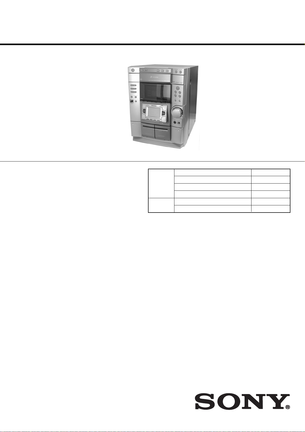
HCD-DP700
SERVICE MANUAL
Ver 1.4 2003.12
• HCD-DP700 is the tuner, deck, CD
and amplifier section in MHCDP700.
CD CD Mechanism Type CDM58E-30BD60
Section Base Unit Name BU-30BD60
Tape deck Model Name Using Similar Mechanism NEW
Section T ape Transport Mechanism Type TCM-230MWR41
US Model
Canadian Model
AEP Model
E Model
Model Name Using Similar Mechanism NEW
Optical Pick-up Name A-MAX.3
SPECIFICATIONS
AUDIO POWER SPECIFICATIONS:
(HCD-DP700 US model only)
POWER OUTPUT AND T OTAL
HARMONIC DISTORTION:
with 8 ohm loads both channels driven, from 120-10 kHz; rates 100
watts per channel minimum RMS power, with no more than 10%
total harmonic distortion from 250 milliwatts to rated output.
Total harmonic distortion less than 0.07%
(8 ohms at 1 kHz, 50 W)
Amplifier section
US, Canadian model:
Continuous RMS power output (reference)
100 + 100 watts
(8 ohms at 1 kHz, 10% THD)
Total harmonic distortion less than 0.07%
(8 ohms at 1 kHz, 70 W)
European model:
DIN power output (rated) 60 + 60 watts
(8 ohms at 1 kHz, DIN)
Continuous RMS power output (reference)
80 + 80 watts
(8 ohms at 1 kHz, 10% THD)
Music power output (reference)
150 + 150 watts
(8 ohms at 1 kHz, 10% THD)
Other models:
The following measured at AC 120, 220, 240 V 50/60 Hz
DIN power output (rated) 130 + 130 watts
(6 ohms at 1 kHz, DIN)
Continuous RMS power output (reference)
180 + 180 watts
(6 ohms at 1 kHz, 10% THD)
Inputs
GAME IN: voltage 450mV,
(phono jacks) impedance 47 kilohms
MD/VIDEO IN: voltage 450/250 mV,
(phono jacks) impedance 47 kilohms
OPTICAL IN:
(Square optical connector jacks, front panel (North American and
European models only), or front and rear panels (except for North
American and European models))
MIC: sensitivity 1 mV,
(Except for North impedance 10 kilohms
American and
European models)
(mini jack)
— Continued on next page —
9-873-889-15
2003L02-1
© 2003.12
COMPACT DISC DECK RECEIVER
Sony Corporation
Home Audio Company
Published by Sony Engineering Corporaton
Outputs
MD/VIDEO OUT: voltage 250 mV,
(phono jacks) impedance 1 kilohms
PHONES: accepts headphones of
(stereo mini jack) 8 ohms or more
SPEAKER
(Central and South
American models): accepts impedance of 6 to 16 ohms
(Other models): accepts impedance of 8 to 16 ohms
SUB WOOFER: voltage 1 V,
impedance 1 kilohms
CD player section
System Compact disc and digital audio system
Laser Semiconductor laser (λ=780 nm)
Frequency response 2 Hz – 20 kHz (±0.5 dB)
Signal-to-noise ratio More than 90 dB
Dynamic range More than 90 dB
DIGITAL OUT OPTICAL
(Square optical connector jack, rear panel)
Tape player section
Recording system 4-track 2-channel stereo
Frequency response 40 – 13,000 Hz (±3 dB), using Sony TYPE I
(DOLBY NR OFF) cassette
40 – 14,000 Hz (±3 dB), using Sony TYPE II
cassette
Wow and flutter ±0.15% W.Peak (IEC)
0.1% W .RMS (NAB)
±0.2% W.Peak (DIN)
Tuner section
FM stereo, FM/AM superheterodyne tuner
FM tuner section
Tuning range 87.5 – 108.0 MHz
Antenna FM lead antenna
Antenna terminals 75 ohm unbalanced
Intermediate frequency 10.7 MHz
AM tuner section
Tuning range
North American model: 530 – 1,710 kHz
(with the interval set at 10 kHz)
531 – 1,710 kHz
(with the interval set at 9 kHz)
European and Middle Eastern models:
531 – 1,602 kHz
(with the interval set at 9 kHz)
Other models: 531 – 1,602 kHz
(with the interval set at 9 kHz)
530 – 1,710 kHz
(with the interval set at 10 kHz)
Antenna AM loop antenna
Antenna terminals External antenna terminal
Intermediate frequency 450 kHz
General
Power requirements
North American model: 120 V AC, 60 Hz
European model: 230 V AC, 50/60 Hz
Mexican model: 120 V AC, 60 Hz
Other models: 120 V, 220 V or 230 - 240 V AC, 50/60 Hz
Adjustable with voltage selector
European model: 180 watts
Other models: 150 watts
Dimensions (w/h/d) Approx. 280 x 360 x 365 mm
Mass
North American and European models:
Other models: Approx. 12.0 kg
Design and specifications are subject to change without notice.
0.5 watts (during Power Saving Mode)
Approx. 10.5 kg
SAFETY CHECK-OUT
(US model only)
After correcting the original service problem, perform the
following safety checks before releasing the set to the customer:
Check the antenna terminals, metal trim, “metallized” knobs, screws,
and all other exposed metal parts for A C leakage. Check leakage as
described below.
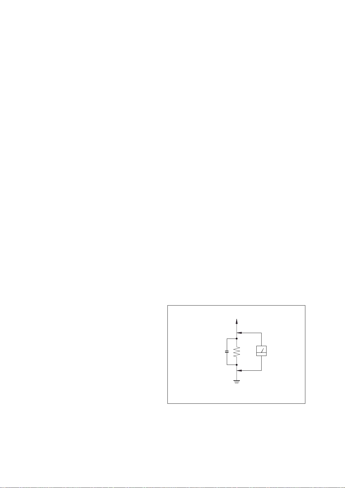
LEAKAGE
The A C leakag e from any exposed metal part to earth g round and
from all exposed metal parts to any exposed metal part having a
return to chassis, must not exceed 0.5 mA (500 microampers).
Leakage current can be measured by any one of three methods.
1. A commercial leakage tester, such as the Simpson 229 or RCA
WT -540A. Follo w the manufacturers’ instructions to use these
instruments.
2. A battery-operated AC milliammeter. The Data Precision 245
digital multimeter is suitable for this job.
3. Measuring the voltage drop across a resistor by means of a
VOM or battery-operated A C voltmeter . The “limit” indication
is 0.75 V, so analog meters must ha ve an accur ate lo w-v oltage
scale. The Simpson 250 and Sanwa SH-63Trd are e xamples of
a passive VOM that is suitable. Nearly all battery operated
digital multimeters that have a 2V AC range are suitable. (See
Fig. A)
To Exposed Metal
Parts on Set
AC
0.15µF
1.5kΩ
Earth Ground
voltmeter
(0.75V)
Power consumption
US model: 170 watts
Canadian model: 170 watts
SAFETY-RELATED COMPONENT WARNING!!
COMPONENTS IDENTIFIED BY MARK 0 OR DOTTED LINE WITH
MARK 0 ON THE SCHEMATIC DIAGRAMS AND IN THE PARTS
LIST ARE CRITICAL TO SAFE OPERATION. REPLACE THESE
COMPONENTS WITH SONY PARTS WHOSE PART NUMBERS
APPEAR AS SHOWN IN THIS MANUAL OR IN SUPPLEMENTS
PUBLISHED BY SONY.
2
Fig. A. Using an AC voltmeter to chec k A C leakage.
ATTENTION AU COMPOSANT AYANT RAPPORT
À LA SÉCURITÉ!
LES COMPOSANTS IDENTIFÉS P AR UNE MARQUE 0 SUR LES
DIAGRAMMES SCHÉMA TIQUES ET LA LISTE DES PIÈCES SONT
CRITIQUES POUR LA SÉCURITÉ DE FONCTIONNEMENT. NE
REMPLACER CES COMPOSANTS QUE PAR DES PIÈSES SONY
DONT LES NUMÉROS SONT DONNÉS DANS CE MANUEL OU
DANS LES SUPPÉMENTS PUBLIÉS PAR SONY.
NOTES ON HANDLING THE OPTICAL PICK-UP
BLOCK OR BASE UNIT
The laser diode in the optical pick-up block may suffer electrostatic
break-down because of the potential difference generated by the
charged electrostatic load, etc. on clothing and the human body.
During repair, pay attention to electrostatic break-down and also
use the procedure in the printed matter which is included in the
repair parts.
The flexible board is easily damaged and should be handled with
care.
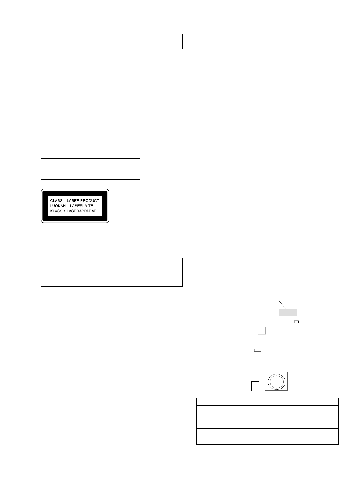
NOTES ON LASER DIODE EMISSION CHECK
The laser beam on this model is concentrated so as to be focused on
the disc reflective surface by the objective lens in the optical pickup block. Therefore, when checking the laser diode emission,
observe from more than 30 cm away from the objective lens.
Laser component in this product is capable
of emitting radiation exceeding the limit for
Class 1.
This appliance is classified as a CLASS 1 LASER product. The
CLASS 1 LASER PRODUCT MARKING is located on the rear
exterior.
6-7. Schematic Diagram Main Section (2/3) ··················· 30
6-8. Schematic Diagram Main Section (3/3) ··················· 31
6-9. Printed Wiring Board DSP Section ·························· 32
6-10. Schematic Diagram DSP Section (1/2)···················33
6-11. Schematic Diagram DSP Section (2/2)···················34
6-12. Printed Wiring Board OPT Section ························ 35
6-13. Schematic Diagram OPT Section ··························· 35
6-14. Printed Wiring Board Front Amp Section (AEP/US/
CND model) ································································· 36
6-15. Schematic Diagram Front Amp Section (AEP/US/
CND model) ································································· 37
6-16. Printed Wiring Board Front Amp Section (E51/MX
model) ··········································································· 38
6-17. Schematic Diagram Front Amp Section (E51/MX
model) ··········································································· 39
6-18. Schematic Diagram Surround Amp Section ··········· 40
6-19. Printed Wiring Board Surround Amp Section ········ 40
6-20. Printed Wiring Board Panel Section ······················· 41
6-21. Schematic Diagram Panel Section (1/2) ················· 42
6-22. Schematic Diagram Panel Section (2/2) ················· 43
6-23. Printed Wiring Board Leaf SW Section·················· 44
6-24. Schematic Diagram Leaf SW Section ···················· 45
6-25. Printed Wiring Board Driver Section······················ 46
6-26. Schematic Diagram Driver Section ························ 47
6-27. Printed Wiring Board Trans Section ······················· 48
6-28. Schematic Diagram Trans Section·························· 49
6-29. IC Pin Function Description ······································· 50
6-30. IC Block Diagrams ····················································· 56
7. EXPLODED VIEWS
7-1. Main Section ································································· 60
7-2. Front Panel Section······················································· 61
7-3. Chassis Section ····························································· 62
7-4. Tape Mechanism Deck Section-1 (TCM-230MWR41) 63
7-5. Tape Mechanism Deck Section-2 (TCM-230AWR41) 64
7-6. CD Mechanism Deck Section (CDM58E-30BD60) ···· 65
7-7. Base Unit Section (BU-30BD60) ································· 66
CAUTION
Use of controls or adjustments or performance of procedures
other than those specified herein may result in hazardous radiation
exposure.
Notes on chip component replacement
• Never reuse a disconnected chip component.
• Notice that the minus side of a tantalum capacitor may be
damaged by heat.
Flexible Circuit Board Repairing
• Keep the temperature of soldering iron around 270˚C
during repairing.
• Do not touch the soldering iron on the same conductor of the
circuit board (within 3 times).
• Be careful not to apply force on the conductor when soldering
or unsoldering.
TABLE OF CONTENTS
1. GENERAL ·········································································· 4
2. DISASSEMBY ·································································· 6
3. TEST MODE ···································································· 13
4. MECHANICAL ADJUSTMENTS ····························· 17
5. ELECTRICAL ADJUSTMENTS ······························· 17
6. DIAGRAMS
6-1. Circuit Board Location ················································· 23
6-2. Block Diagrams ···························································· 24
6-3. Printed Wiring Board BD Section ···························· 26
6-4. Schematic Diagram BD Section ······························· 27
6-5. Printed Wiring Board Main Section ························· 28
6-6. Schematic Diagram Main Section (1/3) ··················· 29
8. ELECTRICAL PARTS LIST ······································· 67
MODEL IDENTIFICATION
— BACK PANEL —
MODEL
US model
CND model
AEP model
MX model
E51 model
• Abbreviation
CND : Canadian model
MX : Mexican model
E51 : Chiri and Peru model
PARTS No.
PARTS No.
4-231-829-0s
4-231-829-1s
4-231-829-2s
4-231-829-5s
4-231-829-6s
3
HCD-DP700
SECTION 1
GENERAL
wg
wd
wa
rj
wh
wf
ws
w;
rh
ql
1
2
3
45
6
8
q;
qs
qd
qf
qg
qh
qj
qk
7
9
qa
rg
rf
rd
rs
wj
wk
wl
ra
e;eaes
el
r;
ek
ed
ef
eg
eh
ej
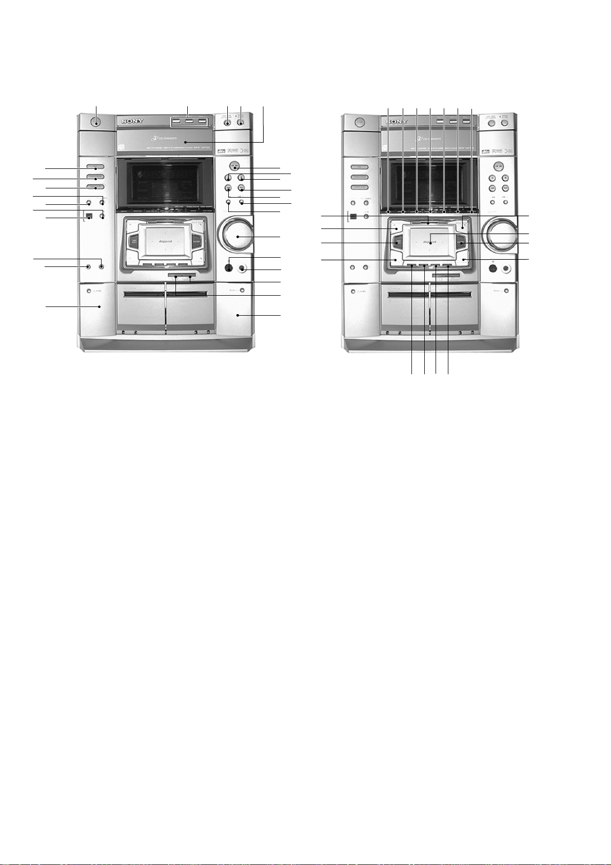
Location of Parts and Controls
1 @/1 (POWER) button
2 DISC 1-3 button
3 DISC SKIP EX-CHANGE button
4 Z OPEN/CLOSE (disc tray) button
5 DISC tray
6 bB (play) button
7 X (pause) button
8 x (stop) button
9 > (go forward) button
q; . (go back) button
qa M/+ (fast forward) button
qs m/– (rewind) button
qd VOLUME control knob
qf IR receptor
qg PHONES jack
qh REC PAUSE/START button
qj CD SYNC HI-DUB button
qk DECK B Z
ql DECK A Z
w; DIGITAL IN (OPTICAL)
wa GAME button
ws DIGITAL button
wd MD (VIDEO) button
wf T APE A/B button
wg TUNER/BAND button
wh CD button
wj DISPLAY
wk SPECTRUM button (US and AEP model only) or
KARAOKE PON button (except for US, AEP model)
wl CLOCK/TIMER SET button
e; TIMER SELECT button
ea EDIT/DIRECTION/PTY (European model only) button
es DOLBY NR/FM MODE/REPEAT button
ed TUNER/MEMORY/PLAY MODE button
ef MOVIE MODE
eg DIGIPAD
eh ENTER
ej TOOL MODE
ek 2CH/MULTI
el EFFECT
r; GROOVE
ra P FILE
rs GAME MODE
rd DSP EDIT
rf MUSIC MODE
rg MULTI CHANNEL DECORDING indicator
rh MIC jack (except for US, AEP model)
rj MIC LEVEL control knob (except for US, AEP model)
4

This section is extracted from
instruction manual.
1
Turn on the system.
2
Press CLOCK/TIMER SET on the
remote.
When you set the time for the first time,
proceed to step 5.
3
Press cursor V/v repeatedly to select
CLOCK SET.
4
Press ENTER.
5
Press cursor V/v repeatedly to set the
hour.
6
Press ENTER.
7
Press cursor V/v repeatedly to set the
minute.
8
Press ENTER.
The clock starts working.
If you have made a mistake or want to change the
time, start over from step 2.
Note
The clock settings are canceled when you disconnect
the power cord or if a power failure occurs.
HCD-DP700
5
HCD-DP700
SECTION 2
DISASSEMBLY
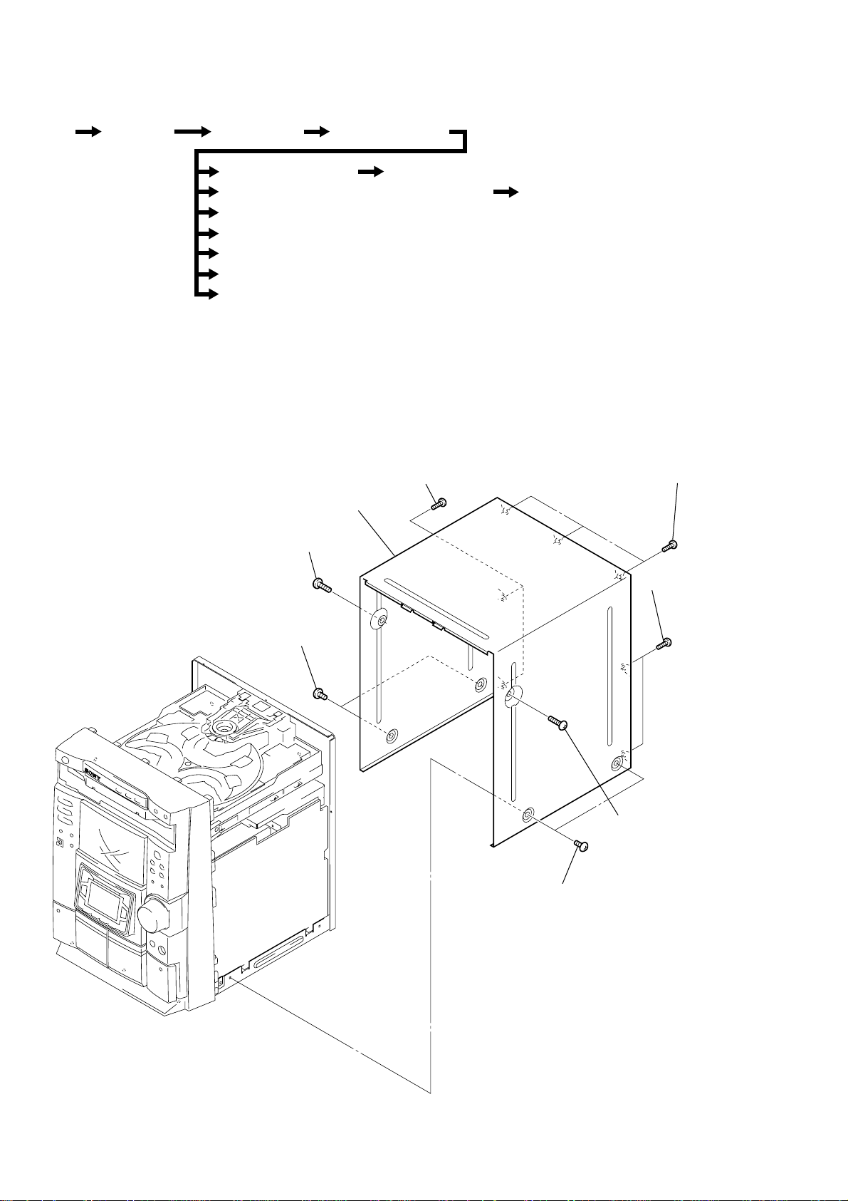
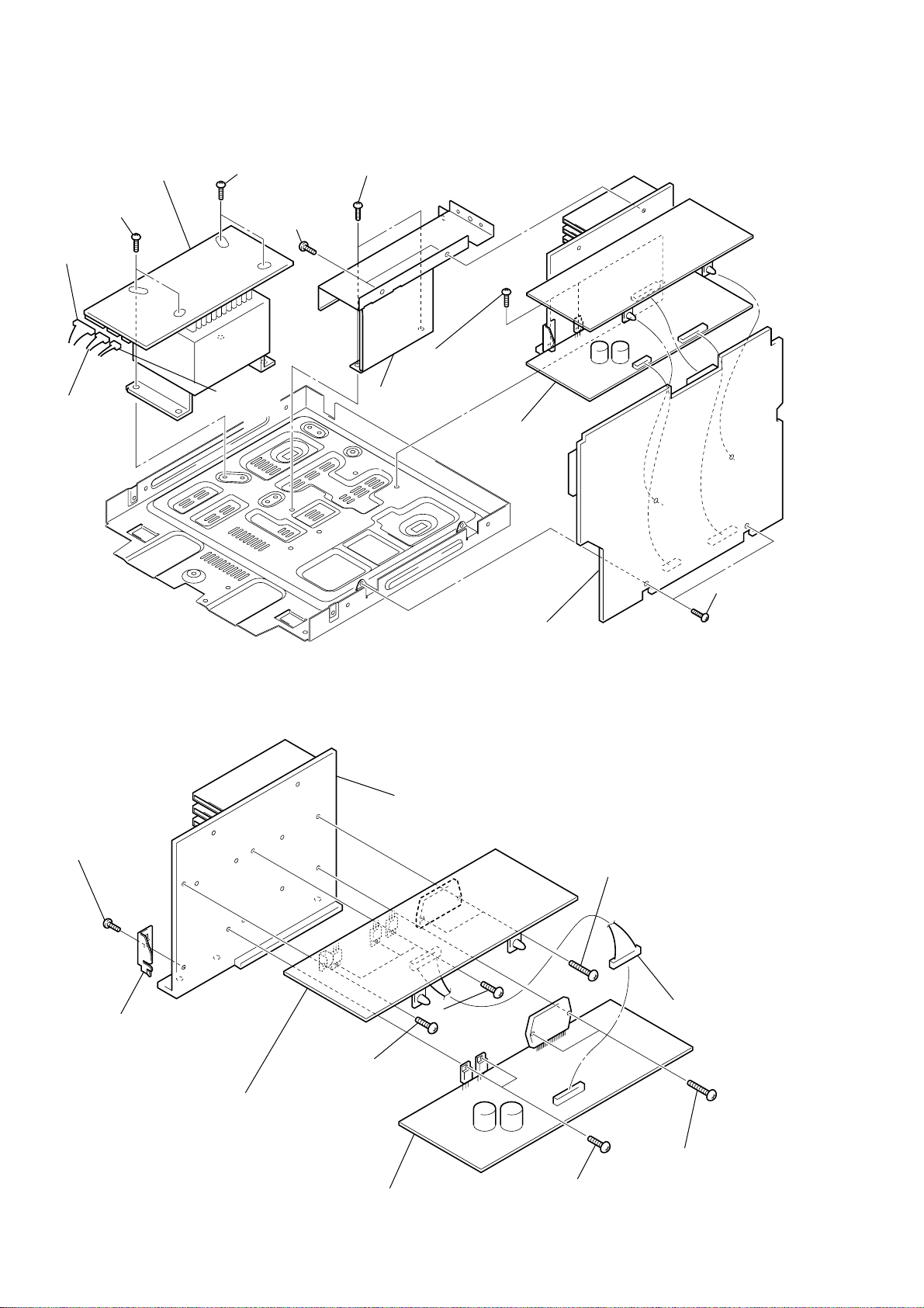
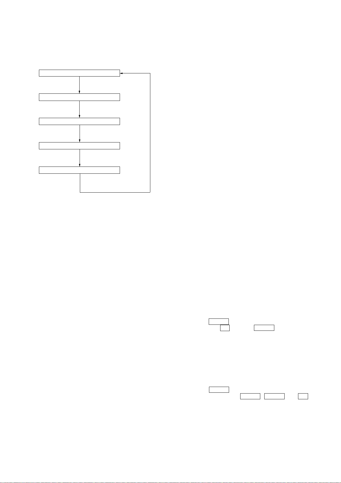
• The equipment can be removed using the following procedure.
Set Case (Top) Loading Panel Front Panel Section
Tape Mechanism Deck
Head (A) Board, Head (B) Board And LEAF SW Board
CD PANEL Board, Panel Board, OPT IN Board
DSP Board And SUB Trans Board
Main Board And Trans Board
FRONT AMP Board And Surround AMP Board
Base Unit
Driver Board, Motor Board And CD Sensor Board
Note : Follow the disassembly procedure in the numerical order given.
2-1. CASE (TOP)
5
two screws (+BVTT 3
8
case
4
screw (case 3 TP2)
×
Escutcheon Pad (With TOUCH PAD)
6
8)
three screws (+BVTT 3
7
(+BVTT 3
×
two screws
×
8)
8)
3
two screws (case 3 TP2)
2
screw (case 3 TP2)
1
two screws (case 3 TP2)
6
2-2. LOADING PANEL
0
two screws (+BVTP 3
× 10
)
3
screw (+BVTP 3
×
10)
2
screw
(+BVTP 3
×
10)
1
connector (CN601)
qs
connector (CN701)
8
connector (CN2)
7
connector (CN1)
6
flat type wire (CN1001)
9
flat type wire (CN201)
4
three screws (+BVTT 3
×
8)
5
front panel section
qa
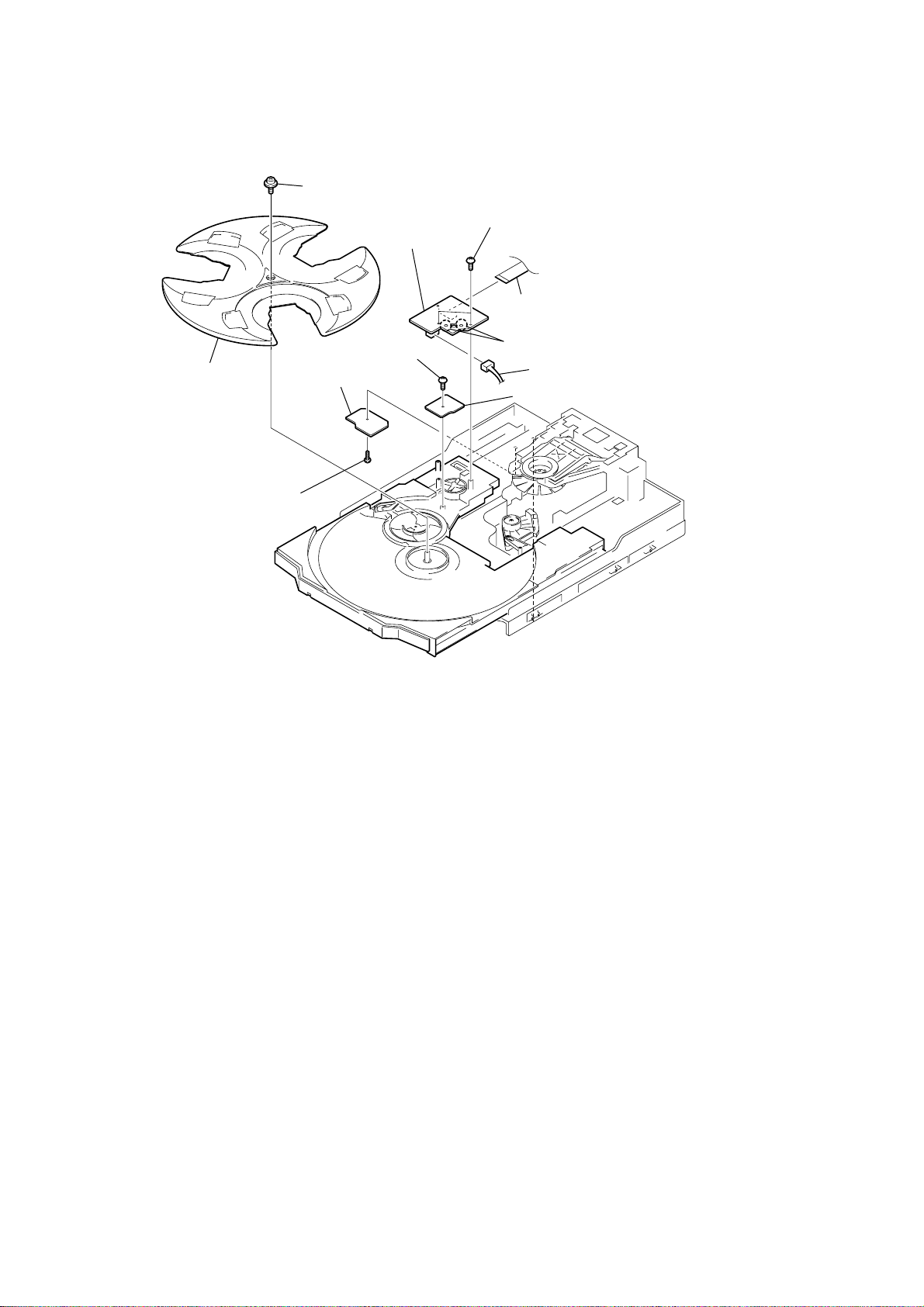
CD mechanism deck (CDM58)
CD mechanism deck (CDM58)
1
Turn the pulley to the direction of arrow.
Front panel side
4
Pull-out the disc tray.
HCD-DP700
pulley
2-3. FRONT PANEL SECTION
2
Pull-out the disc tray.
3
7
HCD-DP700
)
)
2-4. TAPE MECHANISM DECK
2
Tape mechanism deck
1
five screws (+BVTP 2.6
×
8
2-5. CD PANEL BOARD, PANEL BOARD AND OPT BOARD
two claws
qg
flat type wire (CN108)
3
knob (vol)
5
4
two screws
(+BVTP 2.6
qf
PANEL board
ring (vol)
6
cover (vol)
×
8)
two claws
two claws
7
nut
qa
three
screws
(+BVTP 2.6
qs
five screws
(+BVTP 2.6
×
8)
two claws
0
qd
four screws
(+BVTP 2.6
×
8)
qj
PANEL board
×
8)
1
(+BVTP 2.6
2
CD panel board
OPT IN board
qh
two screws
(+BVTP 2.6
8
(+BVTP 2.6
9
five screws
(+BVTP 2.6
five screws
×
8)
four screws
×
8)
×
×
8)
8
8
2-6. ESCUTCHEON PAD (WITH TOUCH PAD)
)
)
)
)
)
1
button (edit)
3
two screws
(+BVTP 2.6
touch pad
7
holder (pad)
6
two screws
(TPG +P 2
×
8)
×
8)
5
two screws
(TPG +P 2
4
escutcheon (pad)
8
three screws
(+BVTP 2.6
2
two screws
(+BVTP 2.6
×
8)
HCD-DP700
×
8)
9
button (DSP
×
8)
2-7. DSP BOARD, SUB TRANS BOARD
qs
connector (CN902)
8
bracket (DSP)
qd
connector
(CN903)
5
connector
(CN601)
9
7
two screws
(+BVTP 3
4
flat type wire (CN602)
×
8)
DSP board
6
two screws
(+BVTP 3
3
flat type wire (CN603)
qa
connector (CN901)
w;
screw
(+BVTP 3
qf
SUB trans board
wa
back panel
×
8)
1
0
two screws
×
8)
(+BVTP 3
wf
two screws
(+BVTP 3
×
8)
ql
screw (+BVTP 3
fan
×
8)
qg
four screws
(+BVTP 3
2
two screws
(+BVTP 3
qh
two screws
(+BVTP 3
wd
two screws
(+BVTP 3
qj
two screws
(+BVTP 3
qk
two screws
(+BVTP 3
×
×
8)
×
8
×
8
×
10
)
×
8
×
8
8)
ws
connector
(CN104)
9
HCD-DP700
)
2-8. MAIN BOARD,TRANS BOARD
4
6
5
two screws
(+BVTT 4
1
connector
(CN914)
2
connector
(CN915)
TRANS board
×
8)
two screws
(+BVTT 4
7
two screws
(+BVTT 3
3
connector
(CN913)
×
8
two screws
×
8)
(+BVTP 3
9
8)
×
8)
0
two
screws
(+BVTP 3
cover (heat sink)
qa
SURROUND AMP
and FRONT AMP
board
×
8)
2-9. FRONT AMP BOARD, SURROUND AMP BOARD
qa
heat sink assy
1
screw
(+BVTT 3
2
bracket
×
8)
qd
8
t
hree screws
(+BVTT 3
MAIN board
×
8)
9
two
screws
(+BVTP 3
qs
two
(+BVTP 3
×
16)
3
connector (CN803
screws
×
8)
10
0
SURROUND AMP board
7
screw
(+BVTT 3
6
FRONT AMP board
×
8)
5
two
screws
(+BVTP 3
4
two
screws
(+BVTT 3
×
8)
×
16)
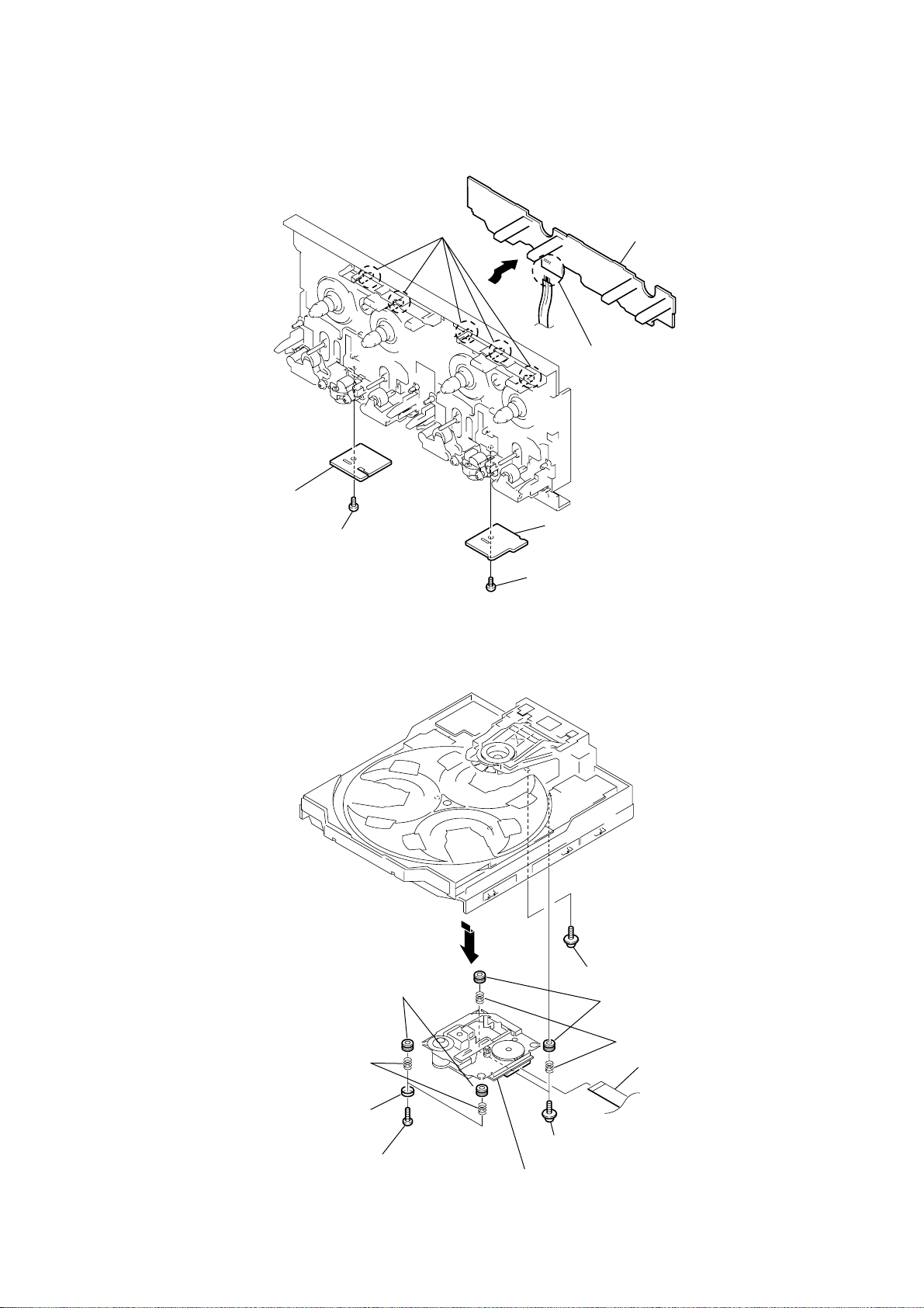
2-10. HEAD (A) BOARD, HEAD (B) BOARD AND LEAF SW BOARD
1
five claws
2
LEAF SW board
3
Remove the four solderings.
HCD-DP700
2-11. BASE UNIT
5
HEAD (A) board
4
screw (+PTT 2
ground point
×
4),
5
6
HEAD (B) board
4
screw (+PTT 2
ground point
×
4),
7
two springs (insulator),
coil
6
two stoppers (BU)
8
two insulators
(BU-30)
4
two screws
(+BVTP 2.6
×
2
screw (DIA. 12), floating
0
two insulators (BU-30)
9
two springs (insulator), coil
1
flat type wire (CN101)
two screws (+PTPWH M2.6), floating
3
8)
qa
base unit
11
HCD-DP700
2-12. DRIVER BOARD, MOTOR BOARD AND CD SENSOR BOARD
8
9
tray
screw (+PTPWH 2.6
0
screw (+BVTP 2.6
2
DRIVER board
5
×
8)
MOTOR board
×
8)
3
two screws (+BVTP 2.6
4
×
8)
6
flat type wire (CN721)
Remove the two solderings of motor.
7
connector(CN722)
qa
CD SENSOR board
1
screw (+BVTP 2.6
×
8)
12

SECTION 3
TEST MODE
HCD-DP700
[Cold Reset]
• The cold reset clears all data including preset data stored in the
RAM to initial conditions. Execute this mode when returning
the set to the customer.
Procedure:
1. Press three buttons STOP , DISPLAY , and DISC 1
simultaneously.
2. The fluorescent indicator tube becomes blank instantaneously,
and the set is reset.
[T uner Step Change] (Except for European and Middle Eastern
models)
• A step of AM channels can be changed o ver between 9 kHz and
10 kHz.
Procedure:
1. Press POWER button to turn the set ON.
2. Select the function “TUNER”, and press TUNER/BAND button
to select the BAND “AM”.
3. Press POWER button to turn the set OFF.
4. Press ENTER and POWER buttons simultaneously, and the
display of fluorescent indicator tube changes to “ AM 9 k STEP”
or “ AM 10 k STEP”, and thus the channel step is changed ov er .
[Function Change Mode]
• Select either VIDEO or MD of the external FUNCTION input.
Procedure:
1. Turn on the power.
2. Hold down MD(VIDEO) button then press POWER button,
and release POWER button f irst in order not in switch off the
set immediately.
The another function of the previous function is selected, the
input level is also changed and displayed “MD” or “VIDEO”.
[GC Test Mode]
• This mode is used to check the software version, FL tube, LED,
keyboard and VACS.
Procedure:
1. Press three buttons STOP , DISPLAY , and DISC 2
simultaneously.
2. LEDs and fluorescent indicator tube are all turned on.
3. When you want to enter the software version display mode,
press DISC 1 .The model number and destination are displayed.
4. Each time DISC 1 is pressed, the display changes stating from
MC version, GC version, CD version, CDDM, CDMA, CDMB,
BDA, BDB, ST version, TA version, TM version, TC version,
in this order, and returns to the model number and destination
display.
5. When DISC 3 is pressed while the version numbers are being
displayed except model number and destination, year, month
and day of the software creation appear . When DISC 3 is pressed
again, the display returns to the software version display . When
DISC 1 is pressed while year, month and day of the software
creation are being displayed, the year, month and day of creation
of the software versions are displayed in the same order of
version display.
6. Press DISC 2 button, and the key check mode is activated.
7. In the key check mode, the fluorescent indicator tube displays
“KOJOVO”. Each time a button is pressed, “KEY” value
increases.
However, once a button is pressed, _it is no longer taken into
account.
“VOL” value increases lik e 1, 2, 3...if rotating VOLUME knob
in “+” direction, or it decreases like 0, 9, 8...if rotating in
“_”direction.
8. Also when DISC 3 is pressed after lighting of all LEDs and FL
tubes, value of VACS appears.
9. T o exit from this mode, press three b uttons in the same manner
as step 1, or disconnect the power cord.
[MC Test Mode]
• This mode is used to check operations of the respective sections
of Amplifier, Tuner , and Tape.
Procedure:
• To enter MC Test Mode
1. Press the POWER button t turn on the set.
2. Press the three buttons of STOP , DISPLAY and DISC 3
simultaneously.
3. Cursor segment flash on the FL display tube. The input
FUNCTION is changed to GAME.
* Check of Amplifier
Initial settings: Input , GAME
EQ , FLAT
Mode , MUSIC
VA CS , OFF
Output channel switching:
MUSIC key: L , LR , R through
MOVIE key: L , SL R , SR through
GAME key:L , L, SL, C R , R, SR, SW through
TOOL key: L , CR , SW through
1. When the VOLUME control knob is turned clockwise even
slightly, the sound volume increases to is maximum and a
message “VOLUME MAX” appears for two seconds, then the
display returns to the original display.
2. When the V OLUME control knob is tuned counter-clockwise
even slightly , the sound volume decreases to its minimum and a
message “VOLUME MIN” appears for two seconds, then the
display returns to the original display.
* Tuner function
1. In the test mode, the default-preset channel is called even when
the TUNER is selected and an attempt is made to call the preset
channel that has been stored in memory. (It means that the
memory is cleared.)
2. The minimum, center and maximum frequency of each band is
set then.
* Tape recording test
1. To enter the MC Test Mode.
2. Load tapes in both tape decks A and B.
3. Press the REC button to start recording.
4. Pressing the M/+ , m/– buttons during recording returns
the tape to the recording start position and stops it at this position.
5. Pressing the “High Speed Dubbing” key while playing back the
tape of deck B switches the playback speed between “Normal
Speed” and “High Speed”.
Note:
When the playback direction of the tape is set to other than “ONY
WAY”, the restriction on the number of times playback which can
be repeated will be cleared.
* AMS Test Mode
1. Set TAPE function
2. Select the desired loop by pressing the PLAY MODE button.
Insert a test tape AMS-110A or AMS-120 to Deck A.
3. Press the SPECTRUM (or KARA OKE PON )b utton to enter
the AMS test mode.
4. After a tape is rewound first, the FF AMS is checked, and the
mechanism is shut off after detecting the AMS signal the AMS
signal twice.
5. Then the REW AMS is checked and the mechanism is shut off
after detecting the AMS signal twice.
13
HCD-DP700
6. When the check is complete, a message of either OK or NG
appears.
* To return to normal mode again.
1. When you want to exit this mode, press the POWER button.
2. The cold reset is enforced at the same time.
[Aging Mode]
This mode can for operation check of tape deck section and CD
section.
• If an error occurred:
The aging operation stops and display then status.
• If no error occurs:
The aging operation continues repeatedly.
Procedure:
1. Press the CD button to select the function “CD”.
2. Load the tapes into the decks A and B respectively.
3. Set a disk in “DISK1” tray.
4. Press the PLAY MODE button to set the “ALL DISCS” mode,
and press the REPEAT button to “REPEAT” off.
5. Press three buttons of ST OP , ENTER , and DISC SKIP/EXCHANGE simultaneously.
6. The aging mode is activated, if the indicator of DOLBY NR is
blinking.
7. To exit from the aging mode, operate the cold reset.
[Tape Deck Section]
• The sequence during the aging mode is following as below.
• If an error occurred, stop display that step.
Aging mode sequence (Tape deck section):
Rewind the tape A and B
“T APE A AG-1”
Shut off
FWD play the tape A
“T APE A AG-2”
2 minutes
Fast forward the tape A
“T APE A AG-3”
Shut off or 20 seconds
RVS play the tape A
“T APE A AG-4”
2 minutes
Rewind the tape A
“T APE A AG-5”
Shut off
FWD play the tape B
“TAPE B AG-2”
2 minutes
Fast forward the tape B
“TAPE B AG-3”
Shut off or 20 seconds
RVS play the tape B
“TAPE B AG-4”
2 minutes
Rewind the tape B
“TAPE B AG-5”
Shut off
14
HCD-DP700
[CD Section]
• The sequence during the aging mode is following as below.
Aging mode sequence (CD section):
Tray Turn
Disc 1 Chucking
TOC Read
Track 1 Play
2 seconds
Last Track Play
2 seconds
Error History Display
1. BD Error History Display
11 digits are displayed after the D character.
Example of display : D00209010100
1st digit : Indicates the error history number.
0 is the latest error
2nd to 3rd digits : Indicates details of the problem.
01 : Cannot focus
02 : GFS NG
03 : Start time over
04 : Focus deviates continuously
05 : Q code absent for some time
4th to 5th digits : Processing when problems occur
01 : Currently SHIP processing
02 : Currently POWER OFF processing
03 : Currently initializing
04 : Currently stopping
05 : Currently STOP operation processing
06 : Currently start processing
07 : Currently TOC reading
08 : Currently searching
09 : Currently playing
0A : Currently pausing
0B : Currently PLAY manual searching
0C : Currently PAUSE manual searching
6th to 7th digits : Operations currently performed for problems
which have occurred
8th to 9th digits : Rotation speed of DISC when problems occur
01 : x1 speed
02 : x2 speed
10th to 11th digits : Fixed at 00
2. CDM Error History <CDM58 Error History Display>
11 digits are displayed after the M character.
Example of display : M0FF400220000
1st digit : Indicates the error history number.
0 is the latest error
2nd to 3rd digits : Indicates the details of the problem.
01 : Initialization table is currently rotating 1
02 : Initialization table is currently rotating 2
03 : Initialization table is currently rotating 3
04 : Currently DISC SKIP in OPEN mode
05 : CLOSE table is currently rotating
06 : Chucking table is currently rotating
07 : Currently performing SHIP operations
08 : Currently performing release operations
09 : Currently performing POWER OFF
operations
4th to 5th digits : Processing when problems occur
01 : Currently performing SHIP operations
02 : Currently performing POWER OFF
operations
03 : Currently initializing
04 : Currently performing release operations
05 : Currently in chuck stop state
06 : Currently performing CLOSE operations
07 : Currently performing exchange CLOSE
operations
08 : Currently performing OPEN operations
09 : Currently performing OPEN POP UP
operations
0A: Currently performing exchange OPEN
operations
6 to 7th digits : Operations currently performed for problems
which have occurred
8th to 9th digits : Targets of processing when problems occur
Same as 4th to 5th digits
10th to 11th digits : Fixed at 00
[CD Ship Mode (No Memory Clear)]
• This mode moves the position to the position durable to vibration Use this mode when returning the set to the customer after
repair.
Procedure:
1. Press POWER button to turn the set ON.
2. Press three CD button and POWER button simultaneously.
3. After the “STANBY” display blinks six times, a message
“LOCK” is displayed on the fluorescent indicator rube, and the
CD ship mode is set.
[CD Ship Mode (Memory Clear)]
• This mode moves the pickup to the position durable to vibration. Use this mode when returning the set to the customer after
repair.
Procedure:
1. Press POWER button to turn the set ON.
2. Press three buttons ENTER , DISC 1 , and CD button
simultaneously.
3. After the “STANDBY” display blinks six times, a message
“LOCK” is displayed on the fluorescent indicator tube, and the
CD ship mode is set.
15

HCD-DP700
[CD Service Mode]
• This mode can run the CD sled motor freely . Use this mode, for
instance, when cleaning the pickup.
Procedure:
1. Press POWER button to turn the set ON.
2. Select the function “CD”.
3. Press three buttons ENTER , DISC 1 , and STOP
simultaneously.
4. The CD service mode is selected.
5. With the CD in stop status, press M/+ button to move the
pickup to outside track, or press m/– button to inside track.
6. To exit from this mode, perform as follows:
1) Move the pickup to the most inside track.
2) Press POWER button to turn the set OFF.
Note:
• Always move the pickup to most inside track when e xiting from
this mode. Otherwise, a disc will not be unloaded.
• Do not run the sled motor excessively, otherwise the gear can
be chipped.
[VACS ON/OFF MODE]
• This mode is used to switch ON and OFF the VACS (Variable
Attenuation Control System).
Procedure:
Press the three buttons STOP , ENTER and SPECTRUM or
KARAOK PON simultaneously.
[VCD COLOR SYSTEM MODE]
• This mode is used for changing the COLOR SYSTEM of THE
VCD.
Procedure:
1. Set the standby mode.
2-1.Press the two buttons POWER and AMS+ simultaneously to
set the COLOR SYSTEM of the VCD to AUTO.
2-2.Press the two buttons POWER and AMS– simultaneously to
fix the COLOR SYSTEM of the VCD to PAL.
2-3.Press the two buttons PO WER and P A USE simultaneously to
fix the COLOR SYSTEM of the VCD to NTSC.
3. The power turns ON automatically and the function sets to “CD”.
4. The FL tube (fluorescent indicator) shows the COLOR
SYSTEM mode set.
5. The COLOR SYSTEM mode set is maintained (memorized)
until COLD RESEY is executed.
[REPEAT 5 LIMIT OFF MODE]
• This mode is used to enable infinite repetitions.
Normally, the number of repetitions allowed is 5.
Procedure:
1. Press the POWER button to turn ON the power supply.
2. Set the function “CD”.
3. Press the three burtons ENTER , DISC 3 , and STOP is
simultaneously.
4. Infinite repetitions is enabled.
5. This state is maintained ( memorized ) until COLD RESET is
executed.
16
SECTION 4
r
MECHANICAL ADJUSTMENTS
HCD-DP700
SECTION 5
ELECTRICAL ADJUSTMENTS
Precaution
1. Clean the following parts with a denatured alcohol-moistened
swab:
record/playback heads pinch rollers
erase head rubber belts
capstan idlers
2. Demagnetize the record/playback head with a head
demagnetizer.
3. Do not use a magnetized screwdriver for the adjustments.
4. After the adjustments, apply suitable locking compound to the
parts adjusted.
5. The adjustments should be perfor med with the rated power
supply voltage unless otherwise noted.
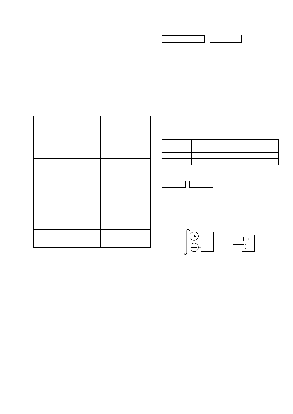
Torque Measurement
Mode
FWD
FWD
back tension
REV
REV
back tension
FF/REW
FWD tension
REV tension
Torque meter
CQ-102C
CQ-102C
CQ-102RC
CQ-102RC
CQ-201B
CQ-403A
CQ-403R
Meter reading
3.06 N • m to 6.96 N • m
31 to 71 g • cm
(0.43 – 0.98 oz • inch)
0.19 N • m to 0.58 N • m
2 to 6 g • cm
(0.02 – 0.08 oz • inch)
3.06 N • m to 6.96 N • m
31 to 71 g • cm
(0.43 – 0.98 oz • inch)
0.19 N • m to 0.58 N • m
2 to 6 g • cm
(0.02 – 0.08 oz • inch)
6.96 N • m to 14.02 N • m
71 to 143 g • cm
(0.98 – 1.99 oz • inch)
9.80 N • m
100 g or more
(3.53 oz or more)
9.80 N • m
100 g or more
(3.53 oz or more)
DECK SECTION
1. Demagnetize the record/playback head with a head
demagnetizer.
2. Do not use a magnetized screwdriver for the adjustments.
3. After the adjustments, apply suitable locking compound to the
parts adjust.
4. T he adjustments should be performed with the rated power
supply voltage unless otherwise noted.
5. The adjustments should be performed in the order given in this
service manual. (As a general rule, playback circuit adjustment
should be completed before performing recording circuit
adjustment.)
6. The adjustments should be performed for both L-CH and RCH.
7. Switches and controls should be set as follows unless otherwise
specified.
• Test Tape
Tape Signal Used for
P-4-A100 10 kHz, –10 dB Azimuth Adjustment
WS-48B 3 kHz, 0 dB Tape Speed Adjustment
P-4-L300 315 Hz, 0 dB Level Adjustment
Record/Playback Head Azimuth Adjustment
0 dB=0.775 V
DECK A DECK B
Note: Perform this adjustments for both decks
Procedure:
1. Mode: Playback
test tape
P-4-A100
(10 kHz, –10 dB)
set
main board
CN301
Pin 3 (L-CH)
Pin 1 (R-CH)
main board
CN301
Pin 2 (GND)
level mete
+
–
17
HCD-DP700
e
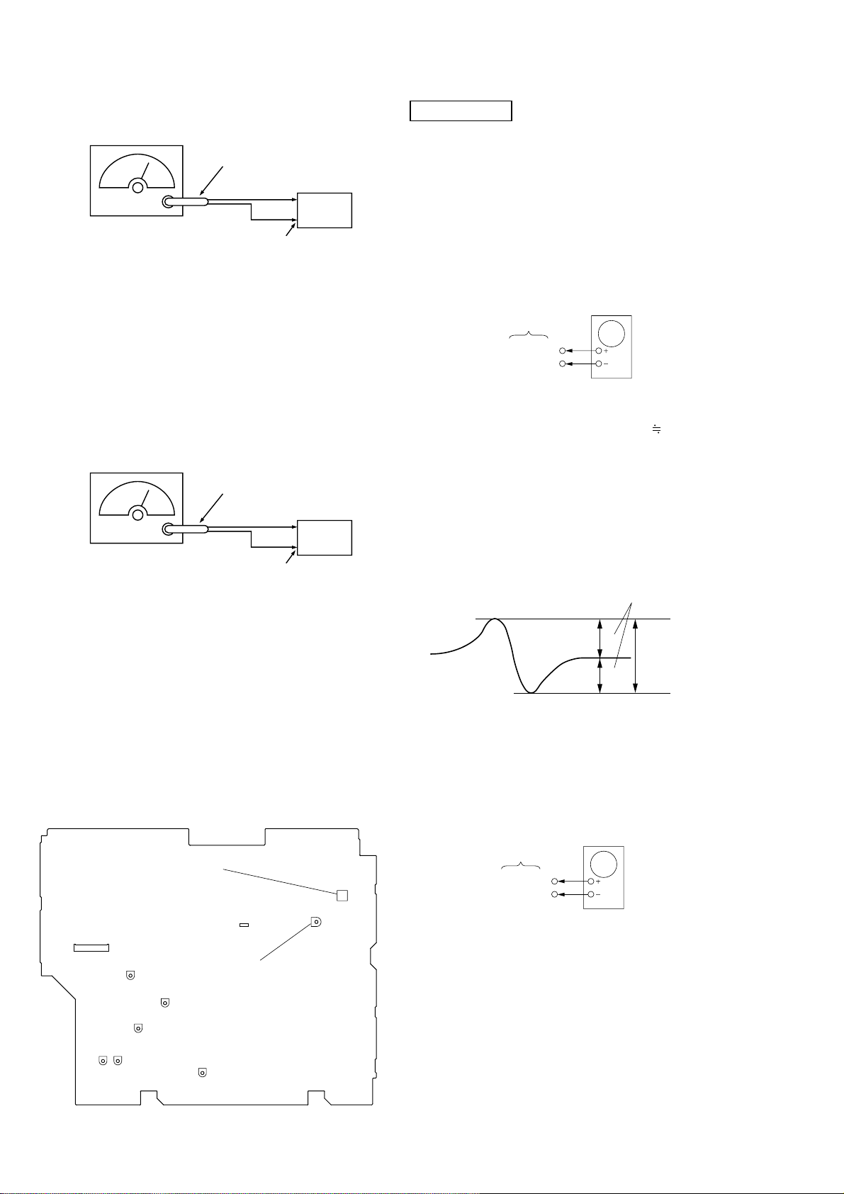
2. Turn the adjustment scre w and check output peaks. If the peaks
do not match for L-CH and R-CH, turn the adjustment screw
so that outputs match within 1dB of peak.
Output
level
within
1dB
L-CH
peak
R-CH
peak
within
1dB
Screw
position
L-CH
peak
Screw
position
R-CH
peak
3. Mode: Playback
test tape
P-4-A100
(10 kHz, –10 dB)
L-CH
MAIN
board
CN301
set
R-CH
waveform of oscilloscope
in phase 45° 90° 135° 180°
pin 3
pin 2
L
R
pin 1
good
oscilloscop
V
wrong
H
4. After the adjustments, apply suitable locking compound to the
pats adjusted.
Adjustment Location: Playback Head (Deck A).
Record/Playback/Erase Head (Deck B).
Tape Speed Adjustment DECK B
Note: Start the Tape Speed adjustment as below after setting to the test
mode.
In the test mode, the tape speed is high during pressing the
CD SYNC HI-DUB button.
Procedure:
1. Turn the power switch on.
2. Press the x button, ENTER button and DISC 3 button
simultaneously.
(The “TEST MODE” on the fluorescent indicator tube display
while in the test mode.)
To exit from the test mode, press the ?/1 button.
Mode: Playback
test tape
WS-48B
(3 kHz, 0 dB)
set
main board
CN301 (Pin 3 : L-CH)
frequency counter
+
–
(Pin 1 : R-CH)
1. Insert the WS-48B into the deck B.
2. Press the gG button on the deck B.
3. Press the CD SYNC HI-DUB button in playback mode.
Then at HIGH speed mode.
4. Adjust RV1001 on the LEAF SW board do that frequency
counter reads 6,000 ± 30 Hz.
5. Press the CD SYNC HI-DUB button.
Then back to NORMAL speed mode.
6. Adjust RV1002 on the LEAF SW board so that frequency
counter reads 3,000 ± 15 Hz.
Adjustment Location: LEAF SW board
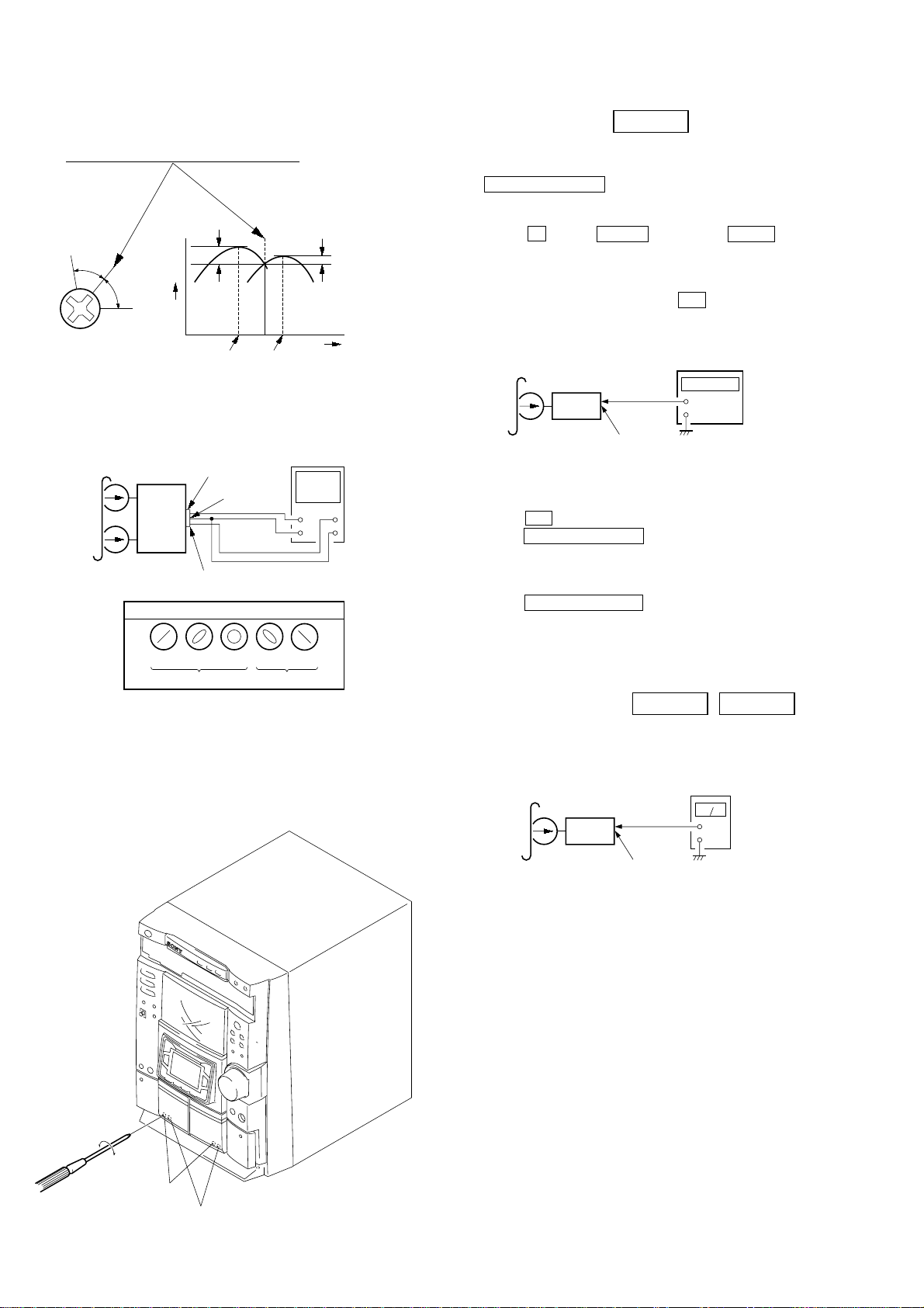
Playback level Adjustment DECK A DECK B
Procedure:
Mode: Playback
test tape
P-4-L300
(315 Hz, 0 dB)
level meter
forward
reverse
set
main board
CN301 (Pin 3 : L-CH)
(Pin 1 : R-CH)
+
–
Deck A is RV302 (L-CH), Deck B is RV303 (L-CH) so that
adjustment within adjustment level as follows.
Adjustment Level:
CN301 PB level: 334.4 to 748.7 mV (–6.8 dB ± –0.5 dB) lev el
difference between the channels: within ±0.5 dB
Adjustment Location: MAIN board
Sample Volue of Wow and Flutter: 0.3% or less W. RMS
(WS-48B)
18
HCD-DP700
e
r
set
MD/VIDEO (AUDIO) IN
315 Hz, 50 mV (–23.8 dB)
blank tape
CS-123
600 Ω
attenuator
AF OSC
+
–
set
recorded
portion
CN301 (Pin 3 : L-CH)
(Pin 1 : R-CH)
level meter
REC Bias Adjustment DECK B
Procedure:
INTRODUCTION
When set to the test mode performed in T ape Speed Adjustment,
when the tape is rewound after recording, the “REC memory mode”
which rewinds only the recorded portion and playback is set.
This “REC memory mode” is convenient for performing this
adjustment. During recording, the input signal FUNCTION will
automatically switch to VIDEO.
(If do not operation of stopped from recording complete, and rotette
of shuttle knob then rewind to recording start position.)
1. Press MD (VIDEO) button to select VIDEO. (This step is not
necessary if the above test mode has already been set.)
2. Insert a tape into deck B.
3. After press REC PAUSE/START button, press REC PAUSE/
START button, then recording start.
4. Mode: Record
MD/VIDEO (AUDIO) IN
1) 315 Hz
2) 10 kHz
AF OSC
attenuator
50 mV (–23.8 dB)
600 Ω
set
blank tap
CN-123
4. Mode: Record
5. Mode: Playback
6. Confirm playback the signal recorded in step 3 become
adjustable level as follows.
If these levels do not adjustable level, adjustment the RV301
(L-CH) and R V351 (R-CH) on the MAIN board to repeat steps
4 and 5.
Adjustable level:
CN301 PB level: 47.2 to 53.0 mV (–27.3 to –26.3 dB)
Adjustment Location: MAIN board
5. Mode: Playback
6. Confirm playback the signal recorded in step 3 become
adjustable level as follows.
If these levels do not adjustable level, adjustment the RV304
(L-CH) and R V354 (R-CH) on the A UDIO board to repeat steps
4 and 5.
Adjustable level: Playback output of 315 Hz to playback output
Adjustment Location: MAIN board
REC Level Adjustment
Procedure:
INTRODUCTION
When set to the test mode performed in T ape Speed Adjustment,
when the tape is rewound after recording, the “REC memory mode”
which rewinds only the recorded portion and playback is set.
This “REC memory mode” is convenient for performing this
adjustment. During recording, the input signal FUNCTION will
automatically switch to VIDEO.
(If do not operation of stopped from recording complete, and rotate
of shuttle knob then rewind to recording start position.)
1. Press MD (VIDEO) button to select VIDEO. (This step is not
necessary if the above test mode has already been set.)
2. Insert a tape into deck B.
3. After press REC PAUSE/START button, press REC PAUSE/
START button, then recording start.
recorded
portion
set
of 10 kHz: ±1.0 dB
level mete
+
–
CN301 (Pin 3 : L-CH)
(Pin 1 : R-CH)
DECK B
[MAIN BOARD] (Component Side)
REC LEVEL (L)
PB LEVEL (L)
(A)
CN304
RV302
RV303
RV354
RV304
REC LEVEL (R)
(A)
[LEAF SW BOARD] (Component Side)
TAPE SPEED
(NORMAL) (HIGH)
RV1002
RV1001
(B)
RV301
RV351
REC LEVEL (L)
(A)
T11
RV11
CN301
PB LEVEL (L)
(B)
REC LEVEL (R)
(B)
CN1001
19
HCD-DP700
FM Tuned Level Adjustment
FM RF SSG
75 Ω coaxial
set
Carrier frequency : 98 MHz
Modulation : AUDIO 1 kHz, 75 kHz
deviation (100%)
Output level : 28 dB (at 75 W open)
FM ANTENNA terminal
(TM601)
Procedure:
1. Supply a 28 dB 98 MHz signal from the ANTENN A terminal.
2. Tune the set to 98 MHz.
3. Adjust RV11 to the point (moment) when the TUNED indicator
will change from going off to going on.
Adjustment Location: MAIN board
Null Adjustment
FM RF SSG
75 Ω coaxial
set
Carrier frequency : 98 MHz
Modulation : AUDIO 1 kHz, 75 kHz
deviation (100%)
Output level : 60 dB (at 75 W open)
FM ANTENNA terminal
(TM601)
CD SECTION
Note :
1. CD Block is basically designed to operate without adjustment.
Therefore, check each item in order given.
2. Use LUV-P01 (4-999-032-01) unless otherwise indicated.
3. Use an oscilloscope with more than 10MΩ impedance.
4. Clean the object lens by an applicator with neutral detergent
when the signal level is low than specified value with the
following checks.
S-Curve Check
Oscilloscope
BD board
TP(FE)
TP(DVC)
Procedure :
1. Connect oscilloscope to TP (FE).
2. Connect between TP (FE) and TP (DVC ( 1.65 V) by lead
wire.
3. Turn Power switch on.
4. Load a disc (LUV-P01) and actuate the focus search. (In
consequence of open and close the disc tray, actuate the focus
search)
5. Confirm that the oscilloscope waveform (S-curve) is
symmetrical between A and B. And confirm peak to peak level
within 2 ±0.5 Vp-p.
S-curve waveform
symmetry
Procedure:
1. Supply a 60 dB 98 MHz signal from the ANTENN A terminal.
2. Tune the set to 98 MHz.
3. Measure voltage between pin 21 of IC 601. Adjust T11 ubtil
the voltage becomes 0 V.
Adjustment Location: MAIN board
Adjustment Location
[MAIN BOARD] Component side
NULL
T11
RV11
CN304
RV302
CN301
FM TUNED LEVEL
RV301
RV303
A
within 4 ±1Vp-p
B
6. After check, remove the lead wire connected in step 2.
Note : • Try to measure several times to make sure than the ratio
of A : B or B : A is more than 10 : 7.
• Take sweep time as long as possible and light up the
brightness to obtain best waveform.
RF Level Check
oscilloscope
BD board
TP(RFDC)
TP(RFAC)
Procedure :
1. Connect oscilloscope to TP2 (RFDC) and TP1 (RFAC).
2. Turned Power switch on.
3. Load a disc (LUV-P01) and playback.
4. Confirm that oscilloscope waveform is clear and check RF signal
level is correct or not.
20
RV354
RV304
RV351
HCD-DP700
)
e
DVC
RFAC
FE
SE
TE
RFDC
Note: Clear RF signal waveform means that the shape “◊” can be
clearly distinguished at the center of the waveform.
RF signal waveform
RF signal waveform
VOLT/DIV : 200mV
TIME/DIV : 500ns
level : 1.45 ± 0.3Vp-p
E-F Balance (1 Track jump) Check
oscilloscop
BD board
TP(TE)
TP(VC)
Procedure:
1. Connect oscilloscope to TP (TE) and TP (DVC) board.
2. Turned Power switch on.
3. Load a disc (LUV-P01) and playback the number nine track.
4. Press the bB button. (Becomes the 1track jump mode.)
5. Confirm that the level B and A (DC voltage) on the oscilloscope
waveform.
Checking Location:
[BD BOARD]
1 track jump waveform
B
0V
level=1.3±0.6Vp-p
Specified level: –– × 100=less than ±22%
A
B
symmetry
6. Adjust RV101 so that A (DC voltage) becomes 0.
1 track jump waveform
center of
waveform
A (DC voltage
21
HCD-DP700
SECTION 6
DIAGRAMS
THIS NOTE IS COMMON FOR PRINTED WIRING BOARDS AND SCHEMATIC DIAGRAMS.
(In addition to this, the necessary note is printed in each block.)
Note on Schematic Diagram:
• All capacitors are in µF unless otherwise noted. pF: µµF
50 WV or less are not indicated except for electrolytics
and tantalums.
• All resistors are in Ω and 1/
specified.
f
•
• C : panel designation.
Note:
The components identified by mark 0 or dotted
line with mark 0 are critical for safety.
Replace only with part
number specified.
• A : B+ Line.
• B : B– Line.
• H : adjustment for repair.
• Voltages and waveforms are dc with respect to ground
• Voltages are taken with a VOM (Input impedance 10 MΩ).
• Waveforms are taken with a oscilloscope.
• Circled numbers refer to waveforms.
• Signal path.
• Abbreviation
: internal component.
under no-signal (detuned) conditions.
Voltage variations may be noted due to normal produc-
tion tolerances.
Voltage variations may be noted due to normal production tolerances.
F : FM
f : AM
E : PB (DECK A)
d : PB (DECK B)
G : REC (DECK B)
c : digital out
g : MD (VIDEO)
CND : Canadian model
MX : Mexican model
E51 : Chiri and Peru model
4
W or less unless otherwise
Note:
Les composants identifiés par
une marque 0 sont critiques
pour la sécurité.
Ne les remplacer que par une
piéce portant le numéro
spécifié.
Note on Printed Wiring Boards:
• X : parts extracted from the component side.
• : Pattern from the side which enables seeing.
• Indication of transistor.
These are omitted.
Q
B
CE
These are omitted.
C
Q
B
E
22
HCD-DP700
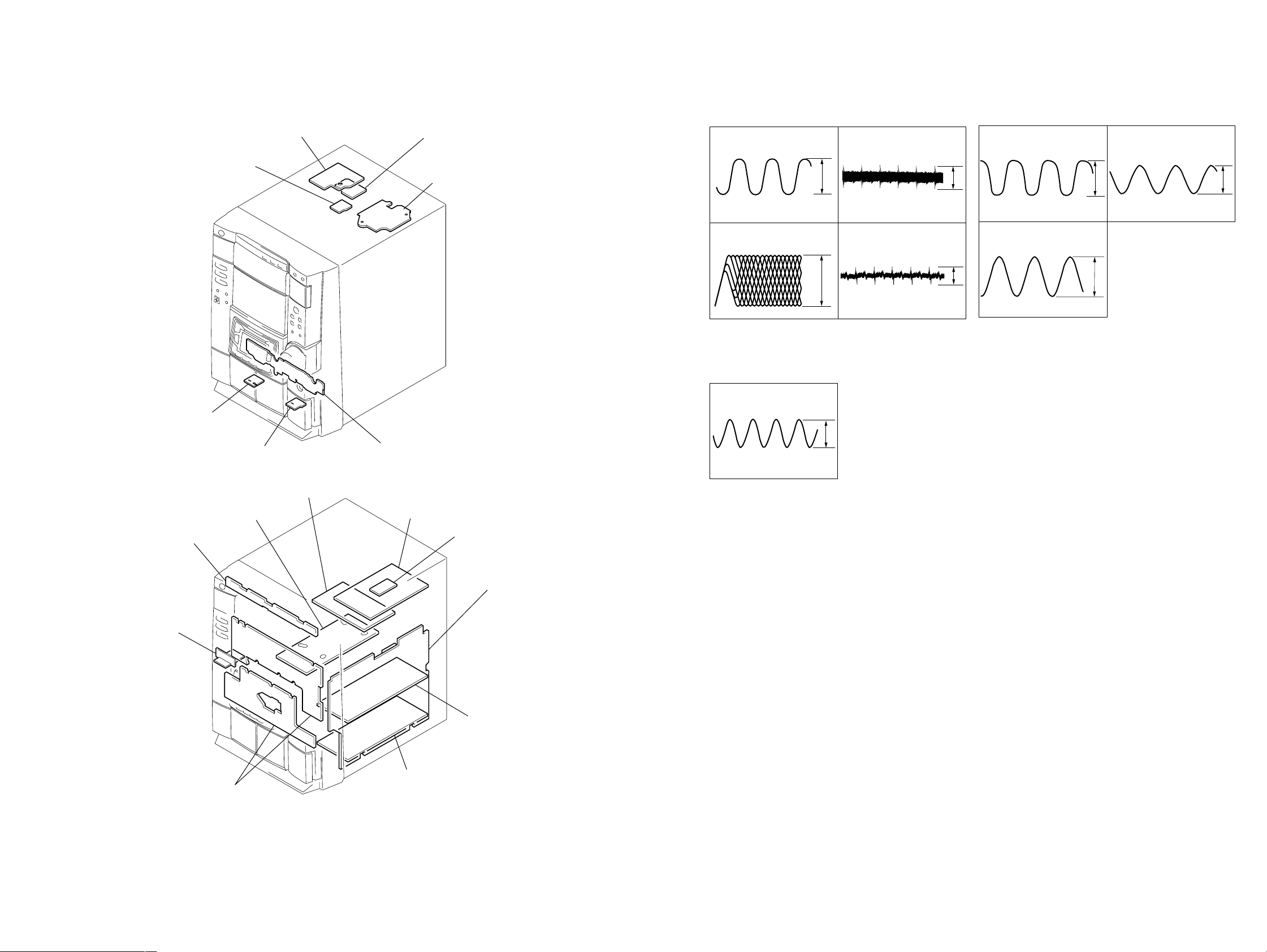
1 IC101 yj (XTAO)
CD PLAY MODE
4.0Vp-p
16.943MHz
1.2Vp-p
2 IC101 ta (RFAC)
CD PLAY MODE
3 IC101 ra (TE)
CD PLAY MODE
4 IC101 el (FE)
CD PLAY MODE
400nsec/div
approx 400mVp-p
approx 170mVp-p
1
IC1101 is (XOUT)
STOP MODE
3Vp-p
4MHz
d
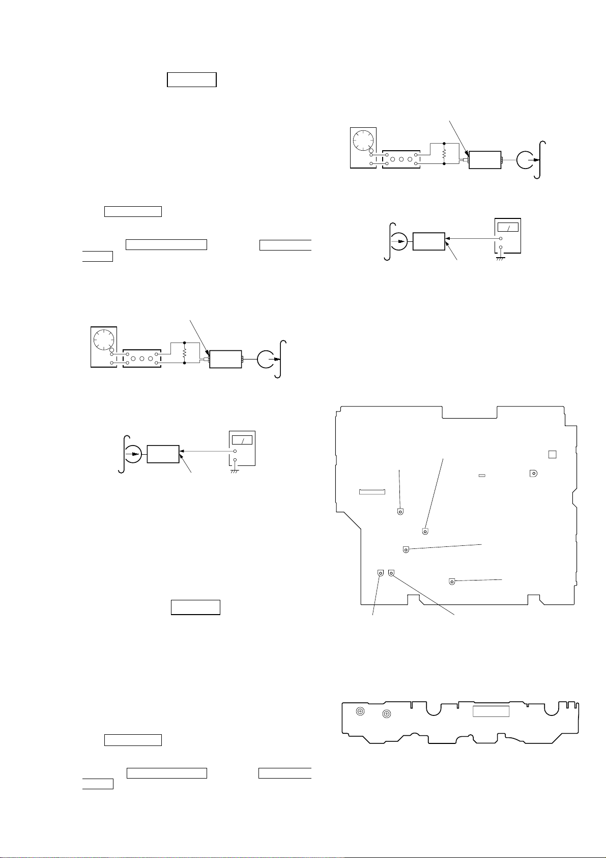
6-1. CIRCUIT BOARD LOCATION
CD SENSOR board
MOTOR board
DRIVER board
BD board
• WAVEFORMS
– BD BOARD –– MAIN BOARD –
1 IC401 qa (XC-OUT)
STOP MODE
32.768kHz
2 IC401 qd (X-OUT)
STOP MODE
16MHz
– PANEL BOARD –
3 T301 4
TAPE B REC MODE
3.0Vp-p
2.8Vp-p
80.1kHz
130Vp-p
HEAD (A) board
CD-PANEL board
OPT IN board
HEAD (B) board
TRANS board
LEAF SW board
SUB TRANS board
DSP board
OPT IN REAR board
(E51, MX only)
MAIN board
SURROUND AMP boar
FRONT AMP board
PANEL board
2323
HCD-DP700
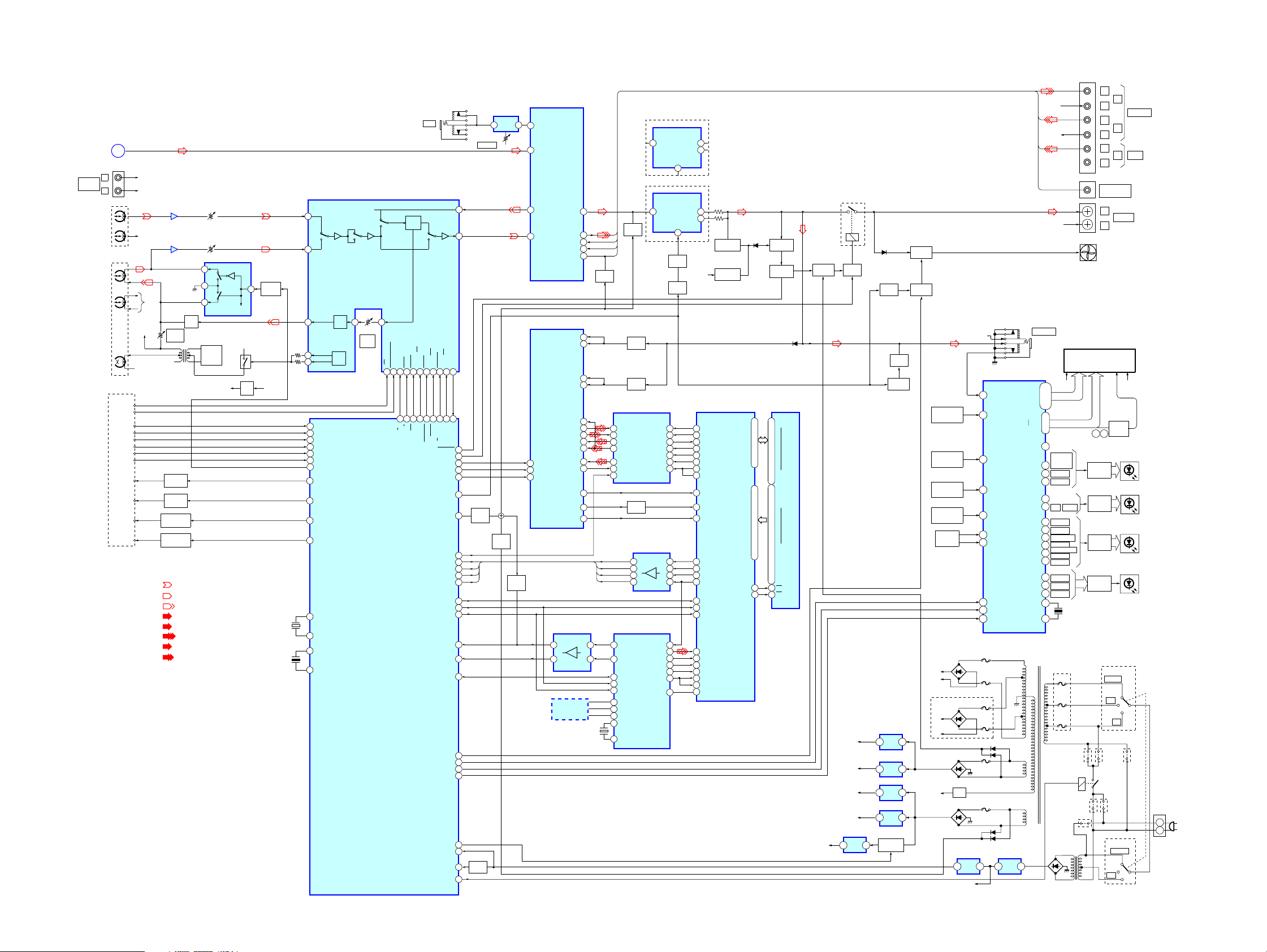
6-2. BLOCK DIAGRAMS
– TUNER/CD SECTION –
TM1
(AEP)
FM 75Ω
G
AM
OPTICAL PICK-UP
TM1
(EXCEPT AEP)
BLOCK
(A-MAX.3)
M102
SLED
MOTOR
M101
SPINDLE
MOTOR
+5V
1
8
11
Q101
LD
DRIVE
M
M
FE1(E51,MX)
FE3(AEP)
IF OUT
ANT IN
FE2(US,CND)
ANT IN
2
49
7
OSC OUT
8
VT
5
IF OUT
1
F OUT
3
VT
4
RB41
IC103
RF AMP
27
VC
6
A
7
B
8
C
9
D
10
E
11
F
1
LD
2
PD
IC102
MOTOR/COIL DRIVE
13
CH1OUTR
14
CH1OUTF
11
CH2OUTR
12
CH2OUTF
18
CH3OUTR
15
CH4OUTF
17
CH3OUTF
16
CH4OUTR
RFDCO
RFDCI
10
15
28
29
FE
16
TE
18
22VCC
12SW
CH1FIN
CH1RIN
CH2FIN
CH2RIN
CH3RIN
MUTE
6
2
3
5
6
23
24CH3FIN
25CH4INSIN
20
VCC
CF1 CF2
+B
(FE1-3)
X51
4.5MHz
1
3
8
7
DIGITAL SERVO
DIGITAL SIGNAL PROC.
51
RFAC
43
RFDC
39
FE
41
TE
40
SE
27
SSTP
32
FFDR
33
FRDR
30
TFDR
31
TRDR
29
SRDR
28
SFDR
26
MDP
Q1
RF IF
AMP
Q2
10
22
16
20
19
18
D/A CONV.
IC101
A+12V
1
D OUT
SCLK
SCOR
SQSO
SENS
XTAI
XTAO
FM
XIN
XOUT
FM OSC
AOUT
AIN
PD
60
20
66
67
PLL
IC51
5DATA
7CLOK
6XLAT
2SQCK
9
1
8
3XRST
IF IN
AM OSC
12
FM
7
15
9VCO STOP
8IF REQ
6DO
4DI
CL
5
CE
3
IC1195
DIGITAL
IN
IC801
DIGITAL
IN
E51,MX
X101
16.9344MHz
LDON
DO
DI
DI
CL
CE
JW1002
SQ-DATA
1
FM IF
RV11
11
AM/FM
24
OSC FM
12
VCO STOP
10
IF REQ MUTE
21
AM RF IN
22
AFC
23
AM OSC
VCC
9
IC608
3
IC608
5
1
IC608
IC551
LEVEL SHIFT
13
11
9 6
AM/FM IF MPX
IC11
AM IF IN
AM MIX OUT
DECORDER
PLL IN OUT
DECORDER
DIGITAL AUDIO
10
DIN0
3
8
DIN1
4
12
5
DIN2
2
4
L OUT
R OUT
IN
TUNED
STEREO
INTERFACE
IC604(2/2)
SPDIF
LPF11
13
14
BUFFER
Q11
R-CH
LPF
L-CH
A
MAIN
SECTION
(Page 25)
4
2
18
17
16
6
7
2
AEP
IFT11
BUFFER
Q81
OPTICAL
IC609
DIGITAL
OUT
OUT
IC81
DECODER
4
DATA
2
DIGITAL OUT
DISPLAY
SWITCH
SWITCH
INT
REMOTE
SENSOR
CD
POWER
16
13
14
IC1102
X801
4.332MHz
S1135
S1115
MASTER CONTROL
IC401(1/2)
18
RDS-INT
20
RDS-DATA
TUNED
88
STEREO
87
21
ST MUTE
DO
23
DI
CL
CE
1
ST-DOUT
25
ST-DIN
27
ST-CLK
CE
22
SIRCS
4
35
CD DATA
37
CD CLK
42
XLT
33
SQ CLK
19
SCOR
32
SQ DATA
SENS
34
BU UP/DOWN SW
73
DISPLAY KEY
74
POWER KEY
43
XRST
40
LDON
LOAD IN
T SENS
44
45LOAD OUT
49
46OPEN SW
47CLOSE SW
48
• RCH is omitted
• Signal Path
IC701
9
MOTOR
DRIVE
7
TBL ADDRESS
SENSOR
: FM
: CD
: DIGITAL OUT
4
2
IC711
OPEN/CLOSE
BU UP/
DOWN
S701
S711
M721
M
TURN
MOTOR
2424
HCD-DP700
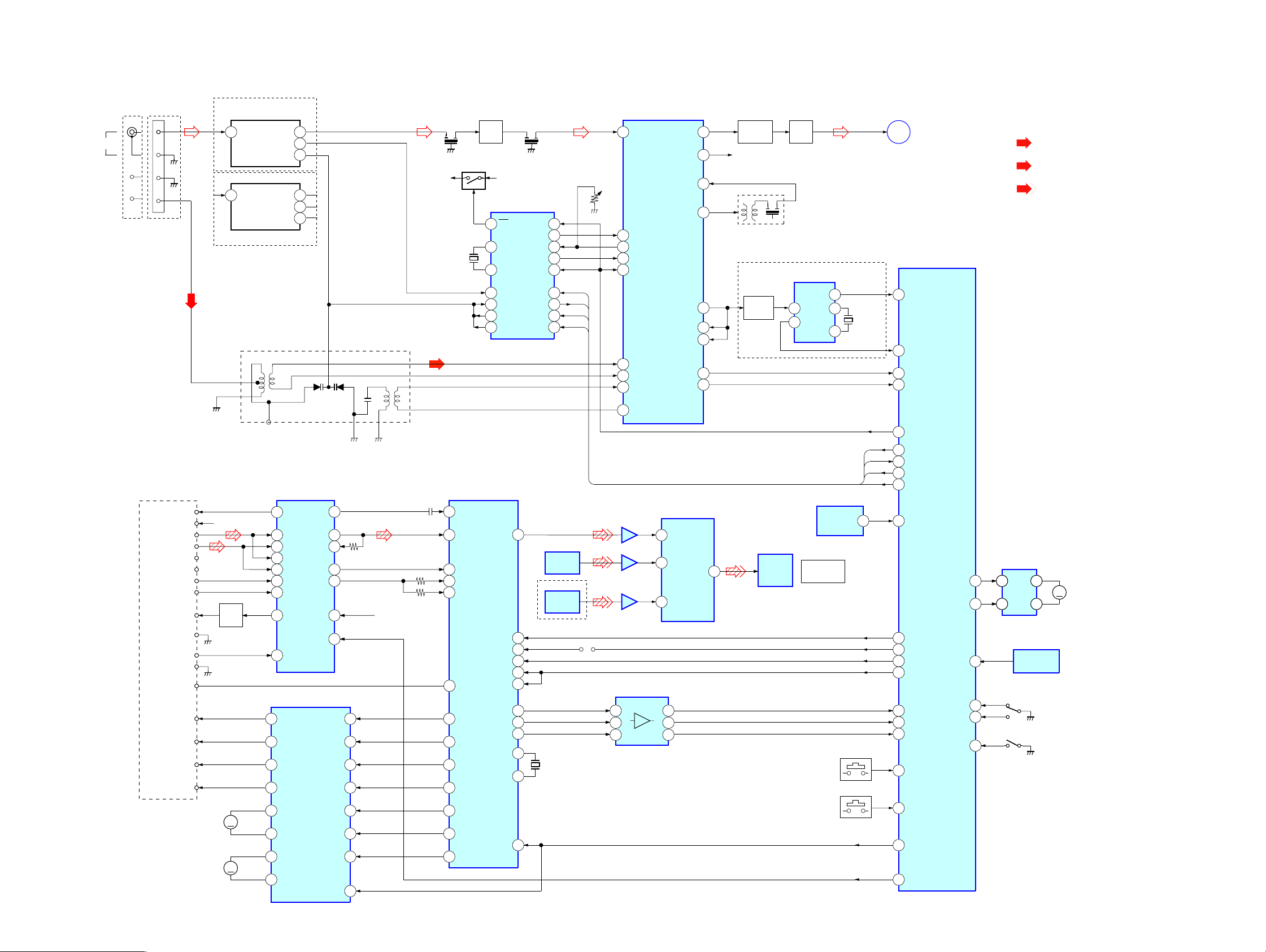
– MAIN SECTION –
L-CH
TUNER
A
SECTION
J101
DECK-A
DECK-B
TC BLOCK
A120/70
B120/70
B SHUT
A SHUT
B PLAY
A PLAY
B HALF
A HALF
A TRG M+
B TRG M+
CAP M H/L
CAP M+
CN304
E+6V
L-CH
R-CH
R-CH
R-CH
R-CH
RV304
E+6V
Q393,394
Q391,392
CAP MOTOR
SPEED CONT
Q396,397
CAP MOTOR
MD/VIDEO
(AUDIO)
HEAD
REC/PB
HEAD
ERASE
HEAD
L
R
PB
PB EQ
AMP
IC303
PB EQ
AMP
IC304
C332,L301
BIAS
TRAP
REC
BIAS(L)
T301
A TRIG
DRIVE
B TRIG
DRIVE
Q395
DRIVE
• RCH is omitted
• Signal Path
: PB (DECK A)
: PB (DECK B)
: REC (DECK B)
: FM
: CD
: MD(VIDEO)
: AM
RV302
RV303
REC/PB SWITCH
1
2
3
BIAS
OSC
Q302,303
+6V
IC302
Q301
R CH
TC A+12V
Q141
DC
BIAS
J601
FIP17
FIP59
FIP/LED5
PLAY1
PB6/AN13
PB6/AN14
PB7/AN15
XOUT
1
PHONES
I
XIN
T911
J1101
2-10
12-22
24-41
43-47
90
100
55
59
67
76
85
86
78
79
80
87
88
89LED1 FIP/LED4
52
53
54PB8/S10 LED13
83
82
L REC OUT
R
R
I
MULTI
CHANNEL
DECODING
EFFECT
GROOVE
LED CTL
REC /
GAME
DIGITAL
MD(VIDEO)
TAPE A/B
TUNER/BAND
TUNER
DISC1
DISC2
DISC3
E51
D902-905
L IN1
L IN4
SWOUT
F1
ENTER
CD
X1101
4.0MHz
F911
F912
F913
JW906
JW905
EXCEPT
E51
TRANSFORMER
IC607(1/2)
MUTE
SWITCH
Q612
1
67
64
70
15
16
17
SOUND PROCESSOR
MAC IN
LIN2
LREC OUT1
FLOUT
LREC OUT
LIN5
SWOUT
IC607(2/2)
SOUND PROCESSOR
FRBB2
FRBB1
FLBB2
FLBB1
L REC IN
ADL+OUT
ADL-OUT
FLIN
SLIN
B PLAY
PORT3
B PLAY
B PLAY
PORT1
PORT4
PORT5
IC603(2/2)
BUFFER
6
2
IC604(1/2)
DIGITAL IN
REFER TO
IC604(2/2)
E51,MX
8
POWER
AEP,UC,CND
46 10
63
66
LIN1
69
LIN4
28
52
51
45
44
2
6
7
9
11
C IN
12
20
18
21
22
5
1
X601
13.5MHz
MUTE
Q611
MUTE
Q604
DBFB
CONT
Q605
DBFB
CONT
MULTI-CHANEL AUDIO DECODE
30
LIN+
LIN-
29
27
LOUT1
25
LOUT2
23
LOUT3
PDN
17
SMUTE
3
Q613
RESET
SWITCH
DSP-RX
12
DSP-DATA
10
DSP-DECODE
8
DIR-UNLOCK
4
IC604(1/2)
DIGITALAUDIO
INTERFACE
17
XSTATE
35
DO
37
CE
DI
36
CL
38
3
DIN0
DIN1
4
DIN2
5
XOUT
21
XIN
22
Q607
IC605
IC603(1/2)
BUFFER
15
MCLK
DATA0
DATA1
DATA2
DATA3
LRCK
ERROR
DATA
LRCK
CKOUT
XMCK
AUDIO
Q821,822
BCK
BCK
POWER
Q823
39
4
9
6
7
8
5
13
11
9
3
34
16
14
15
13
20
24
IC801
AMP
12
IC801
AMP
12
MUTE
MUTE
SWITCH
11
10
11
+B
AUDIO DECODER
SCKOUT
14
BCK
20
SDI1
18
SDO1
23
SDO4
26
SDO3
25
19
LRCKO
GP10
67
BST
56
2
XRST
113
PM
32
HACN
35
HDOUT
68
GP9(DECODE)
59
EXLOCK(ERROR)
36
HCS
33
HD IN
34
HCLK
30
SDI2
29
BCKI2
28
LRCKI2
22
KFSI2
12
MCLK2
9
MCLK1
GP8(AUDIO)
69
Q801
OVER LOAD
DETECTOR
Q816,817
THERMAL
DETECTOR
IC601
WEO
RY881
Q835-837
PROTECT
DETECTOR
D891
Q831,832
PROTECT
CONT
FEED BACK
IC602
S-RAM
72
16
D15
I
I
80
13
•
•
98
10
•
I
99
7
•
•
102
38
I
I
108
35
•
32
D0
I
29
20
64
I
I
18
66
•
•
A15
2
83
I
I
4
85
•
•
1
92
•
I
5
97
•
•
21
109
•
•
24
110
A0
•
•
42
112
I
44
•
27
I
25
61744
CSO
CS
45
WE
D606
Q833,834
PROTECT
SWD+5V
RELAY
DRIVE
TC+9V
A+12V
D+5V
D+3.3V
3
IC931
5VREG
Q881,882
1
D111
Q507
MUTE
IC922
3
REG
IC923
3
REG
IC932
3
REG
IC934
3
REG
Q931,932
B+SWITCH
MUTE
MUTE
SWITCHT
Q111-113
DRIVER
SWITCH
Q121
Q503
1
1
1
1
FAN
Q114
FAN
S1135
DISPLAY
SW
S1136-1138,1140-1147
FUCTION
KEY
S1110-1114
S1129-1134,1139
FUCTION
KEY
S1116-1128
FUCTION
KEY
S1101
VOLUME
D871
+VH
-VH
E51,MX
D1071
B+
B-
D950
VP
D959
Q971
REG
IC501
3
RESET
EVER5.7V
AC1
AC1
AC2
AC2
AC3
AC3
AC4
AC4
R CH
1
58
64
64
65
66
56
57
60
61
77
F914
F915
F916
F917
D830,831
F918
F919
D961,962
DISPLAY CONTROL
IC1101
HEADPHONE
KEY0
KEY0
PB7/SO1 LED11
PA3/AN3 LED10
PB4/AN2 LED9
KEY1
RLED5 FIP/LED0
LED4 FIP/LED1
KEY2
VOL 1A
VOL 1B
LED1 FIP/LED2
LED1 FIP/LED3
PB0/IC1 LED15
PB1/C11 LED14
IIC DATA
IICCLOCK
RSTX
IC901
+5.7V
3
REG
FIP/LED16
POWER TRANSFORMER
Q502
LINE
MUTE
Q501
RESET
SWITCH
RV1201
MICVOL
Q504-506
IC1201
POWER
MUTE
MIC
AMP
J1202
MIC
DECK PROC.
IC301
48
A
B
46
SWITCH
4
Q304,305
EQ OUT(L)
REC
36
NORM
33
BIAS
CROM
SW
32
TC A+12V
B SHUT
90
A SHUT
89
57
B PLAY
A PLAY
56
B HALF
91
70
A HALF
TC RELAY
69
A TRIG
50
B TRIG
52
CAP M H/L
54
55
CAP M CONT
XC IN
10
X401
32.768kHz
X402
16MHz
XC OUT
11
X OUT
13
X IN
15
REC
70
120
38
EQ
RV301
REC(L)
LEVEL
MASTER CONTROL
PB
39
17
IC401(2/2)
DOLBY
B NORM/CROM/METAL
A120/70
PB A/B16NORM/HIGH
18
19
67
66
PB A/B
EQ H/N
REC
B
DOL
PB
PAS
BIAS ON/OFF
ALC ON/OFF15RM ON/OFF22NR ON/OFF23REC /PB/PASS24LM ON/OFF25MS OUT
20
26
68
65
61
60
59
58
BIAS
REC MUTE
NR ON/OFF
SP PROTECT
FRONT RELAY
AMP-DATA
AMP-CLK
AMP-LAT
STK-MUTE
LINE-MUTE
CODEC-SMUTE
DSP-RX
DSP-ACK
DSP-DECODE
DIR-UNLOCK
DSP-CS
DIG-CLK
DIR-STATE
DIR-RX
DIR-CS
IICDATA
M-RESET
CD/DVDPOWER
STBY RELAY
53
TC MUTE
R/PB PAS
DIG-TX
FAN
IICCLK
ACOUT
RESET
AMS IN
ALC
43
40
86
84
1
2
3
72
71
79
6
80
82
15
81
5
7
77
78
76
94
30
29
41
98
100
12
83
J602
M961
FAN
FLOURESCENT
INDICATOR TUBE
E51
RY901
JW901
E51
T901
SUB
SUB WOOFER
FL1101
97 99
Q1107,1111
1112
LED
DRIVER
Q1108-1110,
1113
LED
DRIVER
Q1101-1106
LED
DRIVER
Q1114-1116
LED
DRIVER
E51
L
OUT
R
L
R
L
R
OUT
L
SPEAKER
R
Q1123,1124
GRID
DRIVER
S901(1/2)
230-240
220
120
JW907
EXCEPT
E51
JW902
EXCEPT
E51
E51
S901(2/2)
230-240
120
MD VIDEO
IN
IN
GAME
F2
D1107,1111
1112
D1108,1113
D1101-1106
D1114-1116
JW903
EXCEPT
E51
CN901
2
AC
IN
1
2525
HCD-DP700
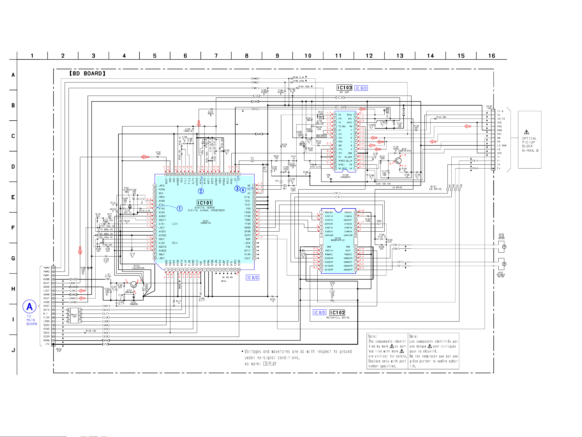
6-3. SCHEMATIC DIAGRAM – BD SECTION – • See page 23 for Waveforms. • See page 58, 59 for IC Block Diagrams. • See page 51, 52 for IC Pin Function.
(Page 29)
2626
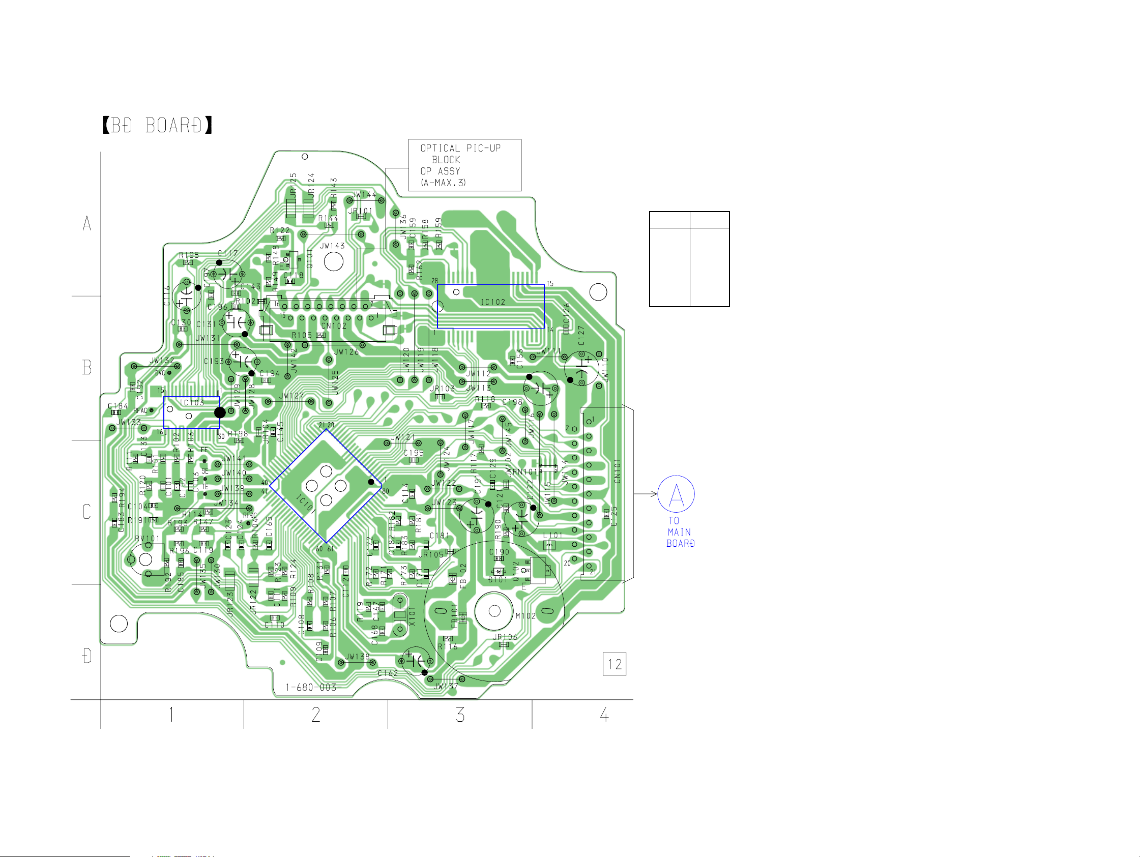
6-4. PRINTED WIRING BOARD – BD SECTION – • See page 23 for Circuit Boards Location.
HCD-DP700
• Semiconductor
Location
Ref. No. Location
D101 C-3
IC101 C-2
IC102 A-3
IC103 B-1
Q101 A-2
Q102 C-3
(Page 28)
2727
 Loading...