

Sony HCDDC-1 Owners manual
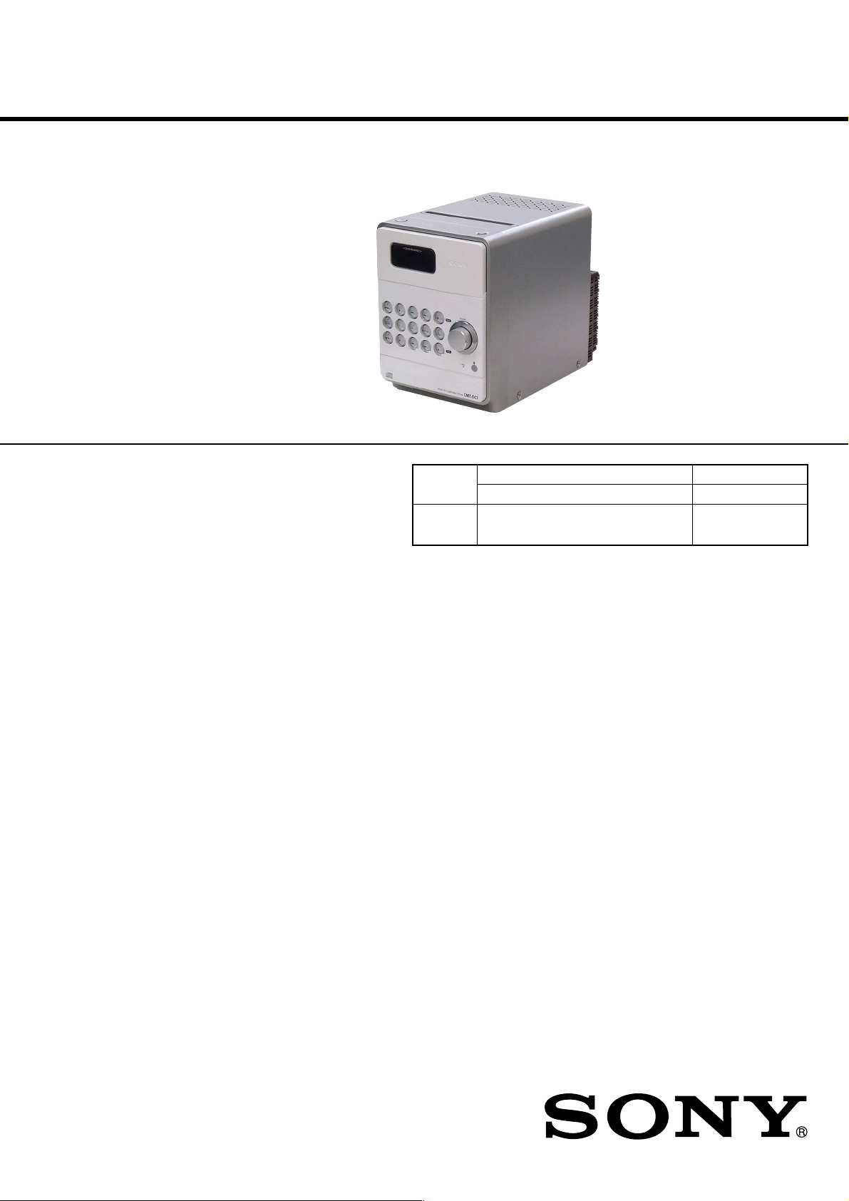
HCD-DC1
SERVICE MANUAL
Ver 1.0 2001.07
HCD-DC1 is the Amplifier, CD player, Tape Deck
and Tuner section in CMT-DC1.
CD
Section
Tape deck
Section
SPECIFICATIONS
AEP Model
UK Model
Model Name Using Similar Mechanism HCD-CP100
CD Mechanism Type CDM55F-K6BD41A
Model Name Using Similar Mechanism HCD-CP100
Amplifier section
DIN power output (rated): 30 + 30 W
Continuous RMS power output (reference):
Music power output (reference):
Inputs
AUDIO IN MD (VIDEO) (phono jacks):
Outputs
OPTICAL DIGITAL OUT (CD):
PHONES (stereo minijack):
SPEAKER: Passive speaker system,
CD player section
System Compact disc and digital
Laser Semiconductor laser
Wavelength 780 - 790 nm
Frequency response 2 Hz - 20 kHz (±0.5 dB)
(6 ohms at 1 kHz, DIN)
35 + 35 W
(6 ohms at 1 kHz, 10%
THD)
85 + 85 W
Sensitivity 500/250 mV,
impedance 47 kilohms
Optical
Accepts headphones with
an impedance of 8 ohms
or more
6 ohms
audio system
(λ = 780 nm)
Emission
duration: continuous
Tape player section
Recording system 4-track 2-channel stereo
Frequency response 50 - 13,000 Hz (±3 dB),
Tuner section
FM stereo, FM/AM superheterodyne tuner
FM tuner section
Tuning range
Antenna FM wire antenna
Antenna terminals 75 ohm unbalanced
Intermediate frequency 10.7 MHz
AM tuner section
Tuning range
Antenna AM loop antenna, external
Intermediate frequency 450 kHz
using a Sony TYPE I
cassette
87.5 - 108.0 MHz
(50-kHz step)
531 - 1,602 kHz
(with the tuning interval
set at 9 kHz)
antenna terminal
General
Power requirements
Power consumption See the nameplate
Dimensions (w/h/d) Approx. 191 × 253 ×
Mass Approx. 5.6 kg
Supplied accessories Remote commander (1)
Design and specifications are subject to change
without notice.
230 V AC, 50/60 Hz
0.5 W (in the standby
mode)
346 mm incl. projecting
parts and controls
AM loop antenna (1)
FM wire antenna (1)
Batteries (2)
Speaker grille net (2)
MICRO Hi-Fi COMPONENT SYSTEM
9-873-181-01 Sony Corporation
2001G0500-1 Home Audio Company
C 2001.7 Shinagawa Tec Service Manual Production Group
HCD-DC1
TABLE OF CONTENTS
1. SERVICING NOTES ............................................... 3
2. GENERAL
Parts Identification .......................................................... 4
Setting the Time .............................................................. 4
3. DISASSEMBLY
3-1. Disassembly Flow ........................................................... 6
3-2. Upper Cover Sub Assy.................................................... 7
3-3. CD Lid ............................................................................. 7
3-4. Front Panel Section ......................................................... 8
3-5. Tape Mechanism Deck.................................................... 8
3-6. CD Mechanism Deck (CDM55F-K6BD41A)................ 9
3-7. Base Unit (BU-K6BD41A)............................................. 9
3-8. Loading Motor Board ..................................................... 10
3-9. Cam (CDM55) ................................................................ 10
4. TEST MODE.............................................................. 11
5. ELECTRICAL ADJUSTMENTS
Deck Section ................................................................... 12
CD Section ...................................................................... 13
6. DIAGRAMS
6-1. Block Diagram – CD SERVO Section – ....................... 15
6-2. Block Diagram – MAIN Section – ................................ 16
6-3. Block Diagram
– DISPLAY/POWER SUPPLY Section – ...................... 17
6-4. Note for Printed Wiring Boards and
Schematic Diagrams ....................................................... 18
6-5. Printed Wiring Board – CD Board – ............................. 20
6-6. Schematic Diagram – CD Board – ................................ 21
6-7. Printed Wiring Board – TC Board – .............................. 22
6-8. Schematic Diagram – TC Board –................................. 23
6-9. Schematic Diagram – MAIN Board (1/3) – ................. 24
6-10. Schematic Diagram – MAIN (2/3)/
LOADING MOTOR/HEADPHONE Boards – ............. 25
6-11. Schematic Diagram – MAIN (3/3)/LCD Boards – ...... 26
6-12. Printed Wiring Boards – MAIN/LCD/
LOADING MOTOR/HEADPHONE Boards – .............. 27
6-13. Printed Wiring Boards
– SWITCH/I/O SWITCH Boards – ................................ 28
6-14. Schematic Diagram
– SWITCH/I/O SWITCH Boards – ................................ 29
6-15. Printed Wiring Board – POWER Board –...................... 30
6-16. Schematic Diagram – POWER Board –......................... 31
6-17. IC Pin Function Description ........................................... 32
Notes on chip component replacement
• Never reuse a disconnected chip component.
• Notice that the minus side of a tantalum capacitor may be damaged by heat.
Flexible Circuit Board Repairing
• Keep the temperature of the soldering iron around 270 ˚C during repairing.
• Do not touch the soldering iron on the same conductor of the
circuit board (within 3 times).
• Be careful not to apply force on the conductor when soldering
or unsoldering.
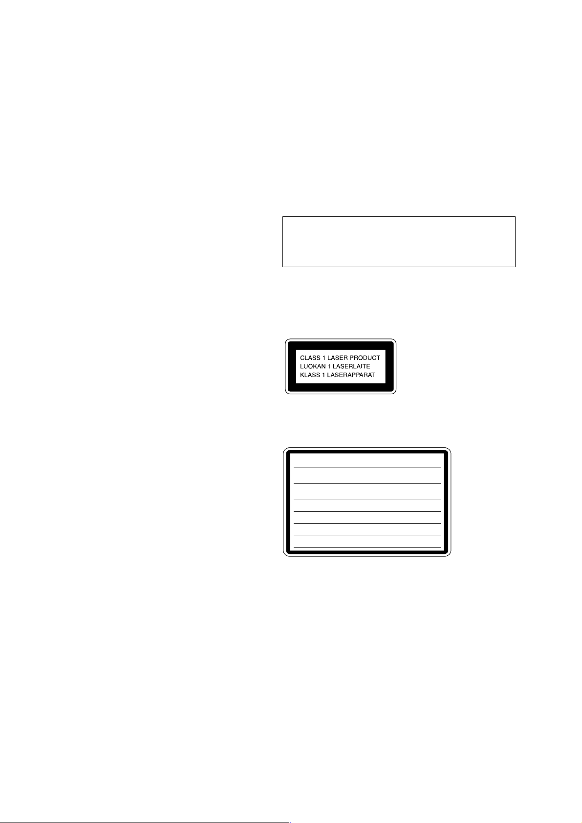
CAUTION
Use of controls or adjustments or performance of procedures
other than those specified herein may result in hazardous radiation exposure.
This appliance is classified as a CLASS 1 LASER product.
The CLASS 1 LASER PRODUCT MARKING is located on
the rear exterior.
Laser component in this product is capable of emitting radiation
exceeding the limit for Class 1.
The following caution label is located inside the unit.
CAUTION :
INTERLOCKS DEFEATED. AVOID EXPOSURE TO BEAM.
ADVARSEL :
SIKKERHEDSAFBRYDERE ER UDE AF FUNKTION. UNDGÅ UDSAETTELSE
FOR STRÅLING.
VORSICHT :
ABDECKUNG GEÖFFNET UND SICHEREITSVERRIEGELUNG
ÜBERBRÜCKT. NICHT DEM STRAHL AUSSETZEN.
VARO! :
TIINA NÄKYMÄTTÖMÄLLE LASERSÄTEILYLLE. ÄLÄ KATSO SÄTEESEEN.
VARNING :
OCH SPÄRREN ÄR URKOPPLAD. BETRAKTA EJ STRÅLEN.
ADVERSEL :
SIKKERHEDSLÅS BRYTES. UNNGÅ EKSPONERING FOR STRÅLEN.
VIGYAZAT! :
GÁRVESZÉLY! KERÜLJE A BESUGÁRZÁST!
INVISIBLE LASER RADIATION WHEN OPEN AND
USYNLIG LASERSTRÅLING VED ÅBNING NÅR
UNSICHTBARE LASERSTRAHLUNG, WENN
AVATTAESSA JA SUOJALUKITUS OHITETTAESSA OLET ALT-
OSYNLING LASERSTRÅLING NÄR DENNA DEL ÄR ÖPPNAD
USYNLIG LASERSTRÅLING NÅR DEKSEL ÅPNES OG
A BURKOLAT NYITÁSAKOR LÁTHATATLAN LÉZERSU-
7. EXPLODED VIEWS
7-1. Upper Cover, Tape Mech Deck Section ......................... 37
7-2. Front Panel Section ......................................................... 38
7-3. Chassis Section ............................................................... 39
7-4. CD Mechanism Deck (CDM55F-K6BD41A)................ 40
7-5. Base Unit (BU-K6BD41A)............................................. 41
8. ELECTRICAL PARTS LIST ............................... 42
2
SAFETY-RELATED COMPONENT WARNING!!
COMPONENTS IDENTIFIED BY MARK 0 OR DOTTED
LINE WITH MARK 0 ON THE SCHEMATIC DIAGRAMS
AND IN THE PARTS LIST ARE CRITICAL TO SAFE
OPERATION. REPLACE THESE COMPONENTS WITH
SONY PARTS WHOSE PART NUMBERS APPEAR AS
SHOWN IN THIS MANUAL OR IN SUPPLEMENTS PUBLISHED BY SONY.
SECTION 1
SERVICING NOTES
HCD-DC1
NOTES ON HANDLING THE OPTICAL PICK-UP
BLOCK OR BASE UNIT
The laser diode in the optical pick-up block may suffer electrostatic break-down because of the potential difference generated
by the charged electrostatic load, etc. on clothing and the human
body.
During repair, pay attention to electrostatic break-down and also
use the procedure in the printed matter which is included in the
repair parts.
The flexible board is easily damaged and should be handled with
care.
NOTES ON LASER DIODE EMISSION CHECK
The laser beam on this model is concentrated so as to be focused
on the disc reflective surface by the objective lens in the optical
pick-up block. Therefore, when checking the laser diode emission, observe from more than 30 cm away from the objecti ve lens.
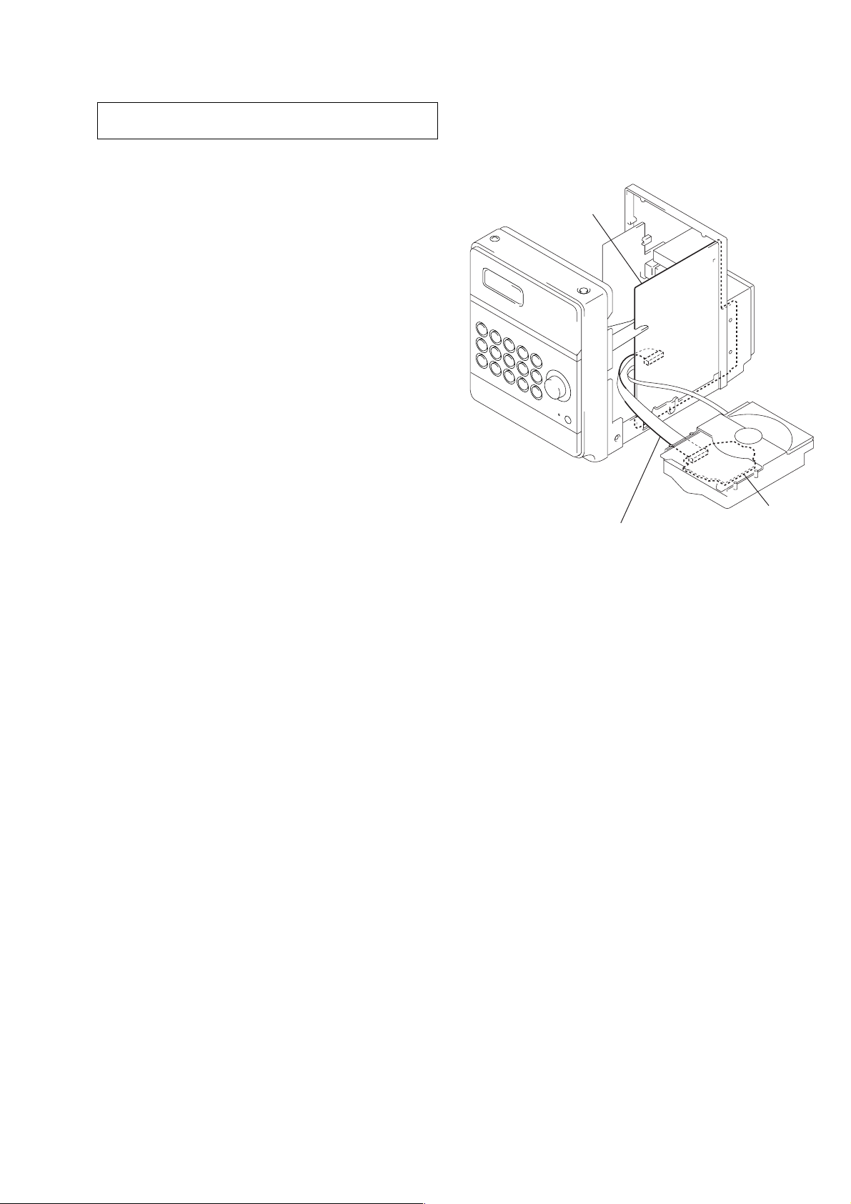
SERVICE POSTION
In checking the CD block, prepare jig (extension cable J-2501011-B).
MAIN board
CD board
Connect jig (extension cable J-2501-011-B)
to the MAIN board (CN101) and CD board (CN101).
3
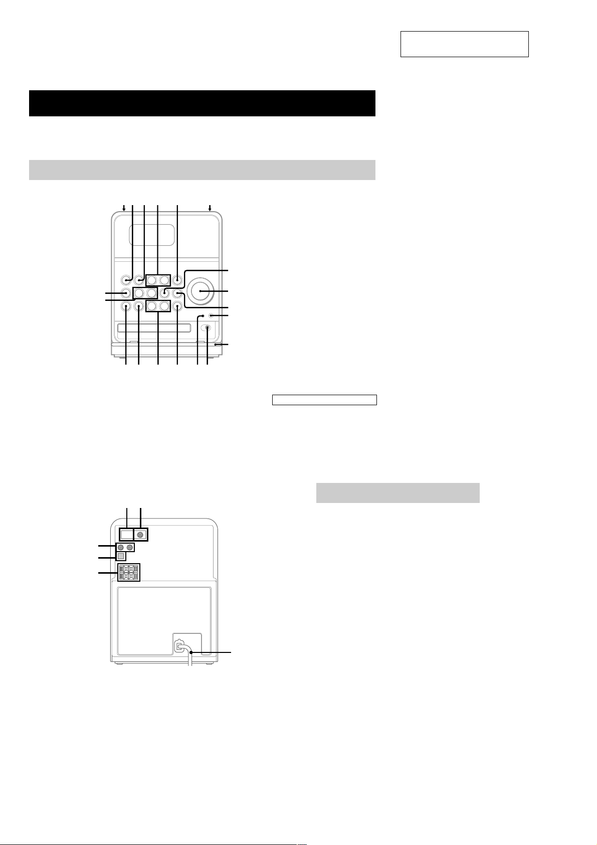
HCD-DC1
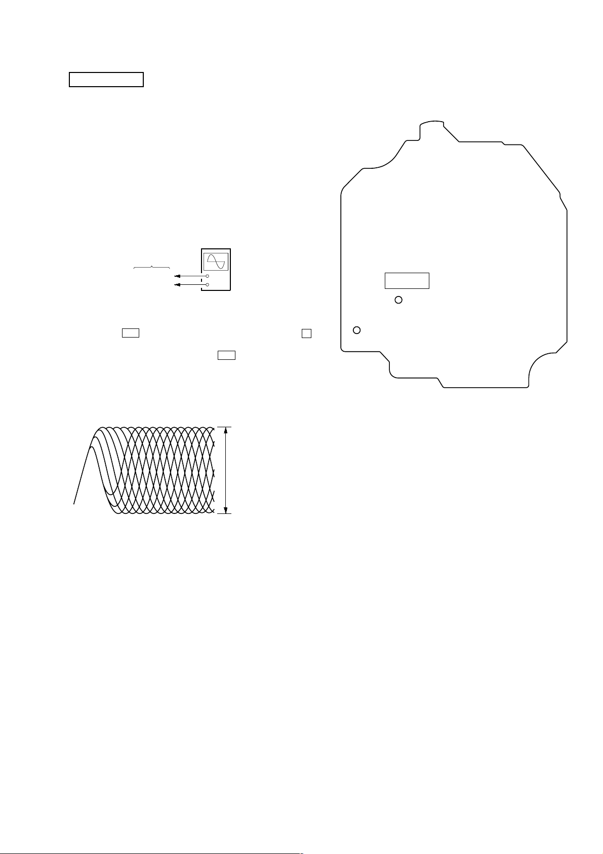
• LOCATION OF CONTROLS
Parts Identification
The items are arranged in alphabetical order.
Refer to the pages indicated in parentheses () for details.
Main unit
SECTION 2
GENERAL
This section is extracted from
instruction manual.
– Front View –
– Rear View –
12
54
63
ql
qk
qf qdqh qgqj
qs
21
3
4
5
1 AM ANTENNA terminals
2 FM ANTENNA jack or terminals
3 AUDIO IN MD (VIDEO) jacks
4 CD DIGITAL OUT OPTICAL connector
5 SPEAKER terminals
6 AC power cord
7
8
9
q;
qa
6
CD cover qa (8, 18)
Shown open in the illustration
above.
CD SYNC 9 (13, 14)
CD .m/M> qg (8, 9,
14)
CD Z qf (8)
CD u qj ( 8, 9)
CD x qh (8, 9, 21)
DSG indicator qd (16)
FUNCTION 7 (8-10, 12-14, 18)
PHONES jack qs (18)
Remote sensor q;
TAPE PAUSE X 5 ( 12-14)
TAPE Y 2 (12-14)
TAPE m/M 4 (12)
TAPE x 3 (12-14, 21)
TUNER/BAND ql (10, 21)
VOLUME 8 (17)
BUTTON DESCRIPTIONS
@/1 (power) 1 (7, 10, 15, 17, 18)
Z 6 (12)
+/– qk (10, 11)
Setting the time
1
Turn on the system.
2
Press TIMER SET on the remote.
If you are setting the clock for the first time,
go to step 5.
3
Press ./> on the remote
repeatedly until “SET CLOCK” appears
in the display.
4
Press ENTER on the remote.
The hour indication flashes.
5
Press ./> on the remote
repeatedly to set the hour.
6
Press ENTER on the remote.
The minute indication flashes.
7
Press ./> on the remote
repeatedly to set the minute.
8
Press ENTER on the remote.
The clock will begin operating.
To reset the system clock
Start over from step 1.
4
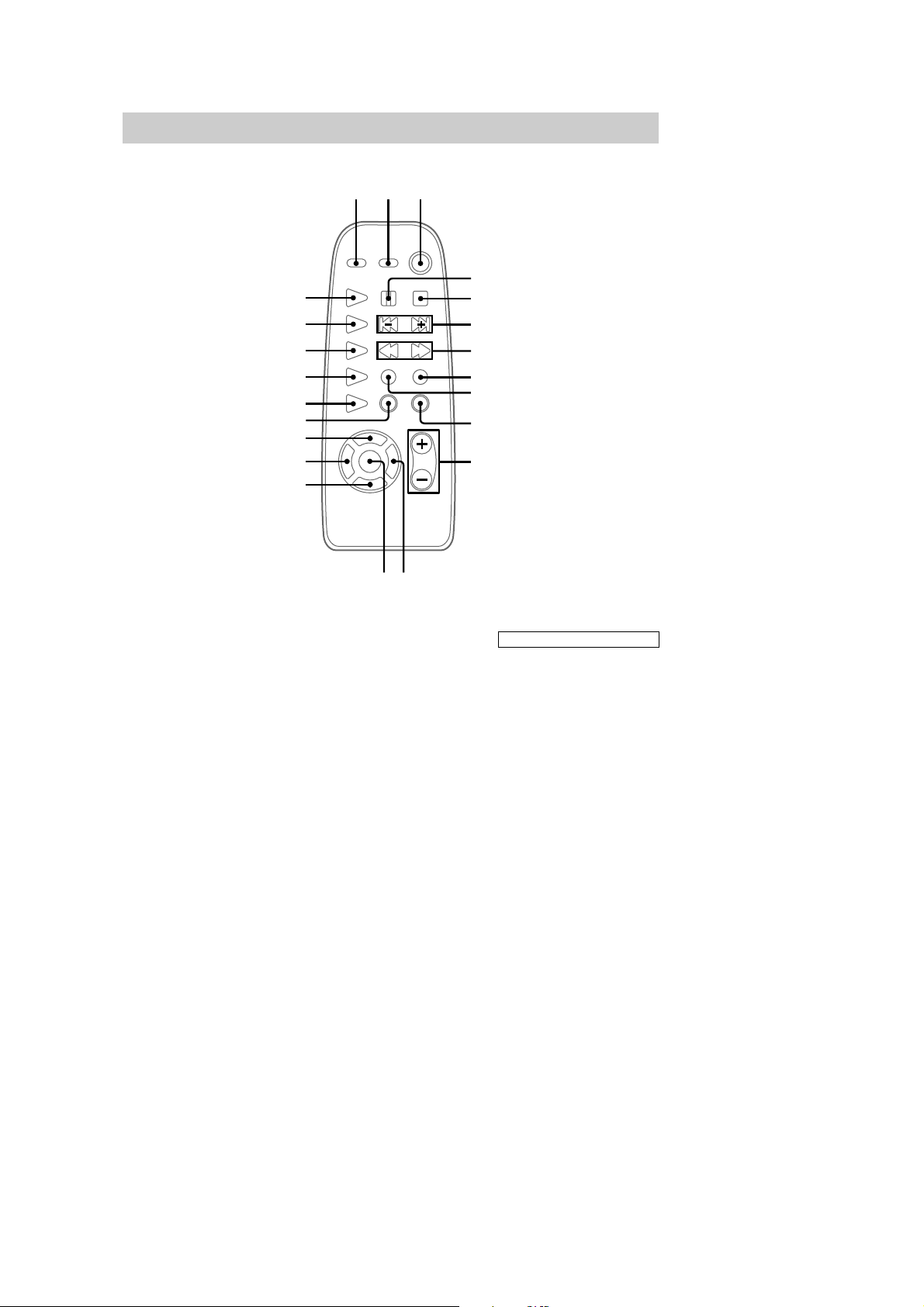
Remote Control
ws
wa
w;
ql
qk
qj
qh
qg
qf
HCD-DC1
123
4
5
6
7
8
9
0
qa
CD REPEAT qk (8)
CD N ws (8, 9)
DIR MODE ql (12-14)
DISPLAY 2 (9, 11)
DSG 1 (16)
ENTER qd (7, 10, 15, 17)
MEMORY qh (10)
PLAY MODE 9 (8, 9, 14)
qsqd
SLEEP qf (16)
STEREO/MONO qj (11)
TAPE Y w; (12-14)
TIMER SELECT qs (15, 17)
TIMER SET qg (7, 15, 17)
TUNER/BAND wa (10)
TUNING MODE q; (10, 11)
VOL +/– qa (17)
BUTTON DESCRIPTIONS
X 4 (8, 12-14)
x 5 (8, 9, 12-14)
./> 6 (7-10, 15, 17)
m/M 7 (8, 10-12)
@/1 (power) 3 (7, 10, 15, 17)
z REC 8 (13)
5
HCD-DC1
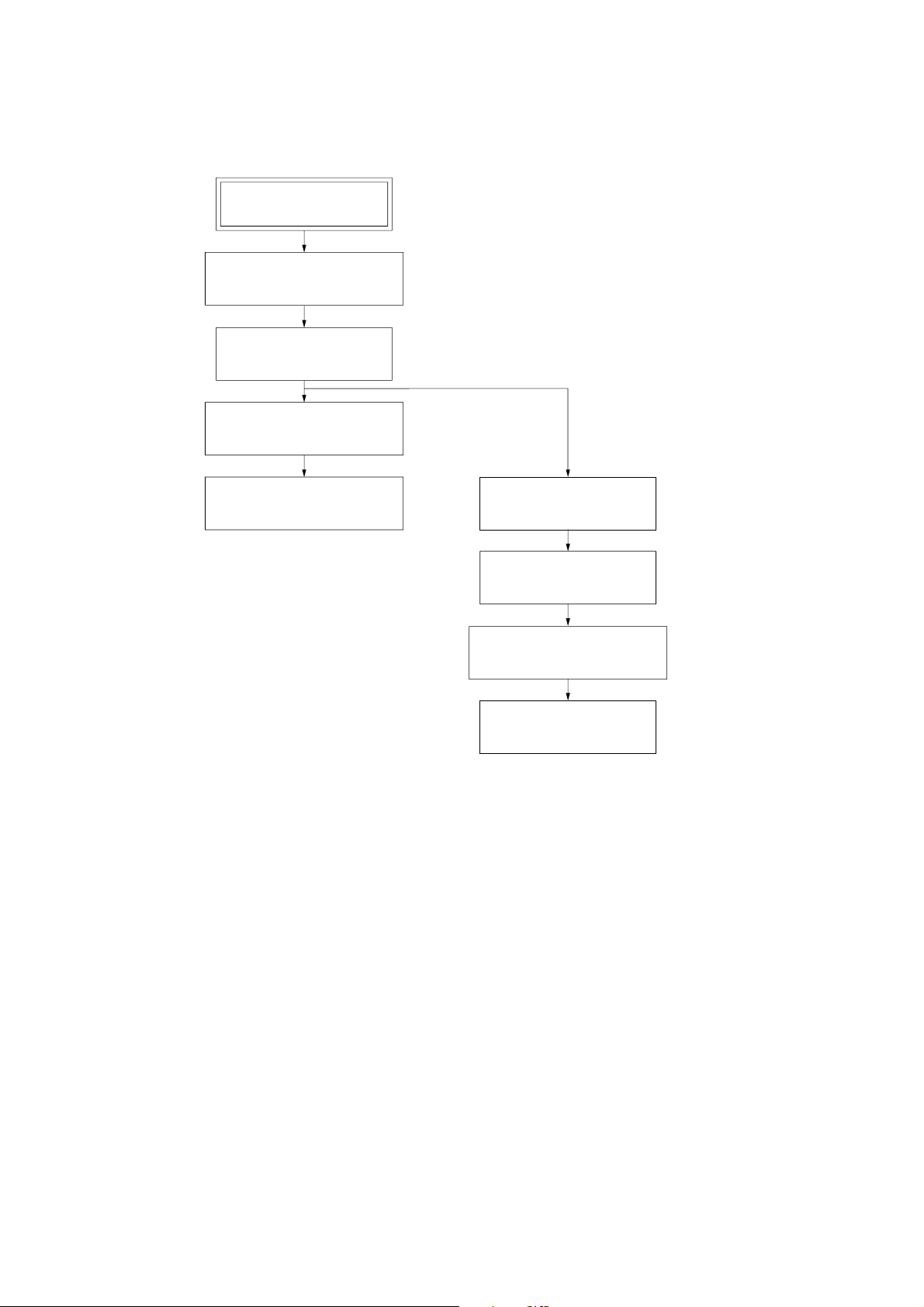
• This set can be disassembled in the order shown below.
3-1. DISASSEMBLY FLOW
SET
SECTION 3
DISASSEMBLY
3-2. UPPER COVER SUB ASSY
(Page 7)
3-3. CD LID
(Page 7)
3-4. FRONT PANEL SECTION
(Page 8)
3-5. TAPE MECHANISM DECK
(Page 8)
3-6. CD MECHANISM DECK
(CDM55F-K6BD41A)
(Page 9)
3-7. BASE UNIT
(BU-K6BD41A)
(Page 9)
3-8. LOADING MOTOR BOARD
(Page 10)
3-9. CAM (CDM55)
(Page 10)
6
Note: Follow the disassembly procedure in the numerical order given.
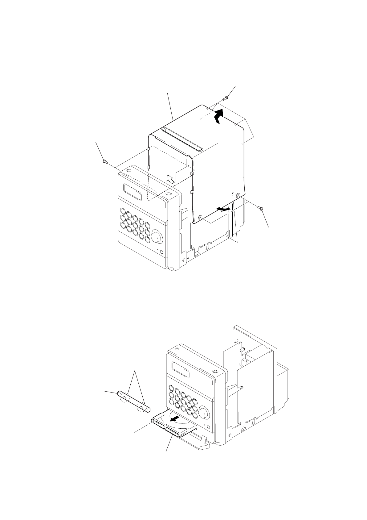
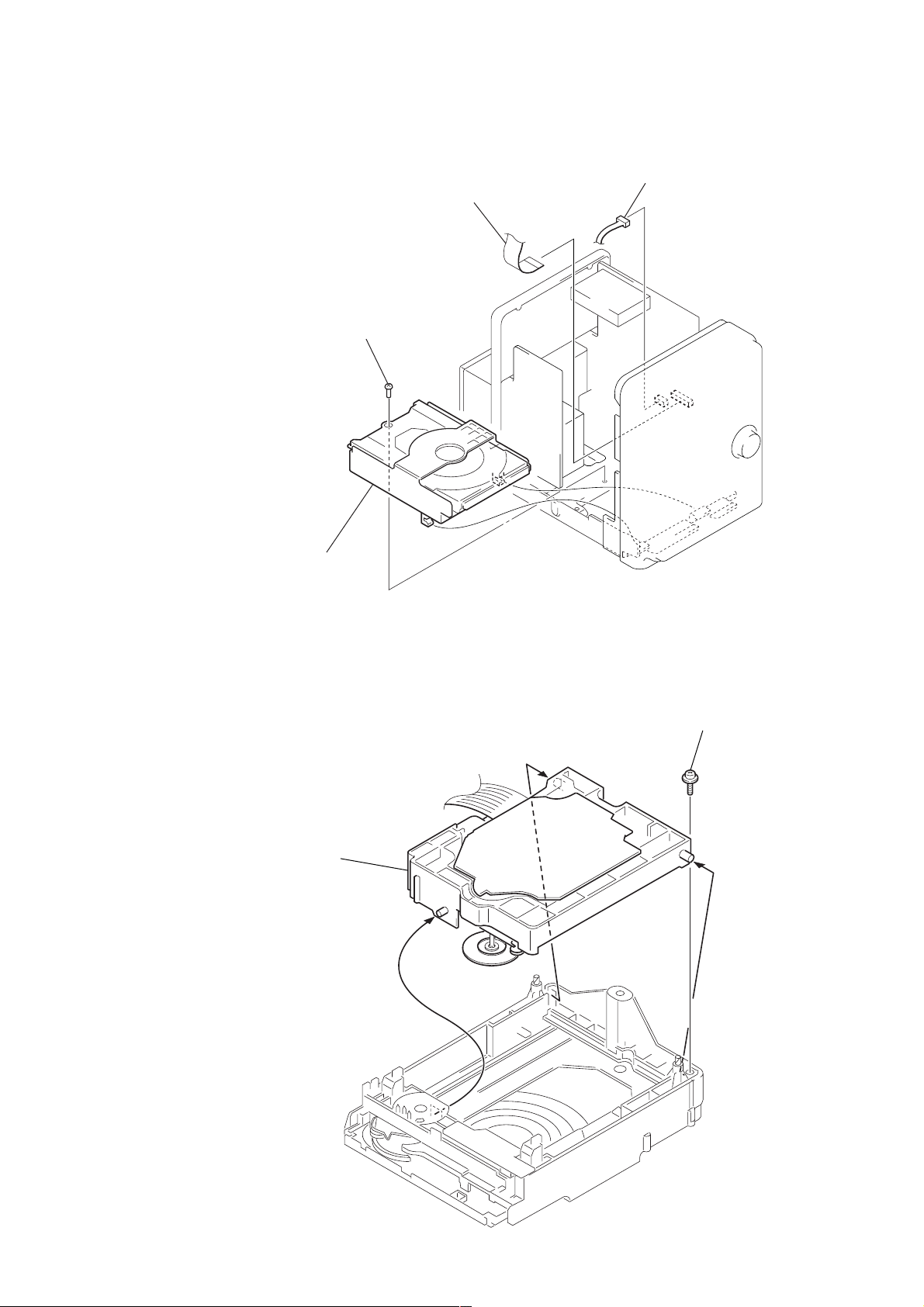
3-2. UPPER COVER SUB ASSY
3
upper cover sub assy
2
two case screws
1
four screws
(BTP3
HCD-DC1
×
8)
3-3. CD LID
3
CD lid
2
two claws
2
two case screws
1
tray
Note: Open the tray by supplying the power.
7
HCD-DC1
r
e
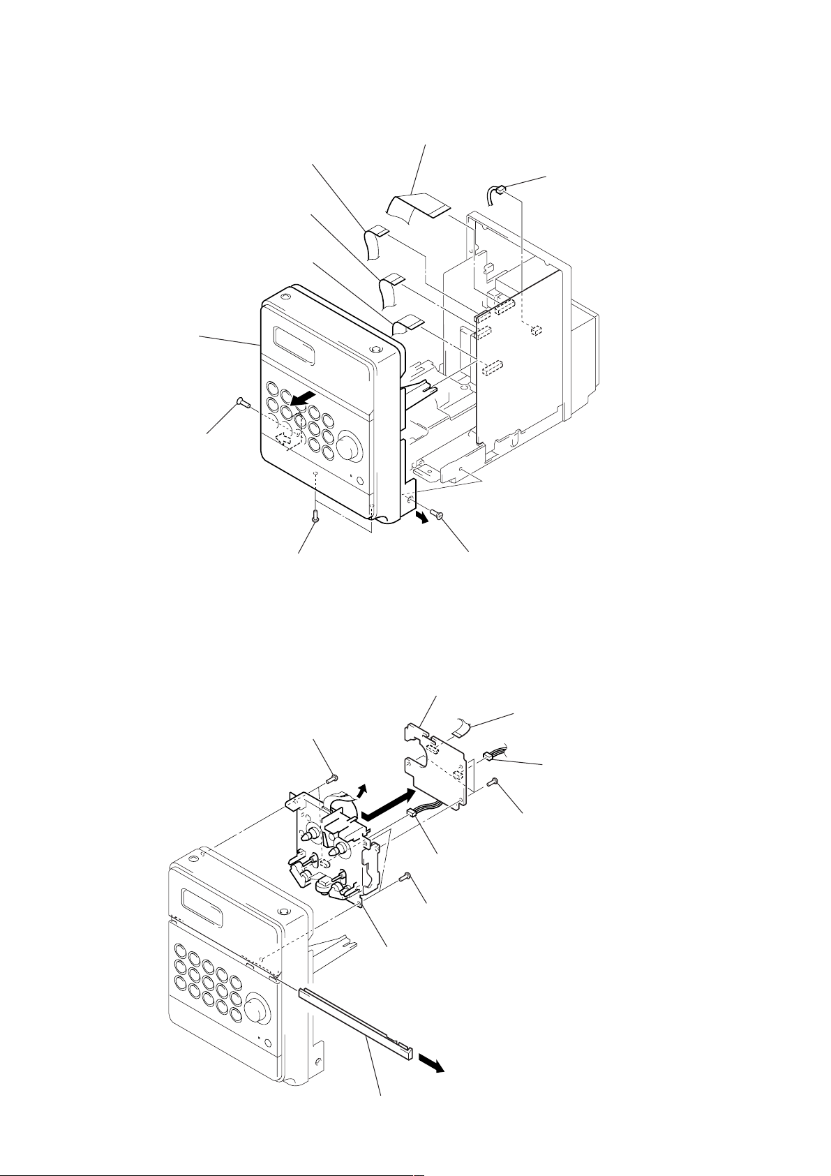
3-4. FRONT PANEL SECTION
1
flexible flat (20core) cable
(CN804)
1
flexible flat (18core) cable
(CN301)
5
front panel section
1
flexible flat (18core) cable
(CN802)
1
flexible flat (16core) cable
(CN801)
2
connecto
(CN501)
4
screw (KTP3 × 6)
3-5. TAPE MECHANISM DECK
3
8
two screws
(BTP3 × 8)
two screws
(BTP3
×
8)
5
7
TC board
4
screw (KTP3 × 6)
2
4
flexible flat (9core) cabl
(CN302)
3
connector
(CN303)
three screws
(BVTT2.6 × 5)
6
connector
(CNP1)
8
two screws
(BTP3 × 8)
9
tape machanism deck
1
azimuth cap
8
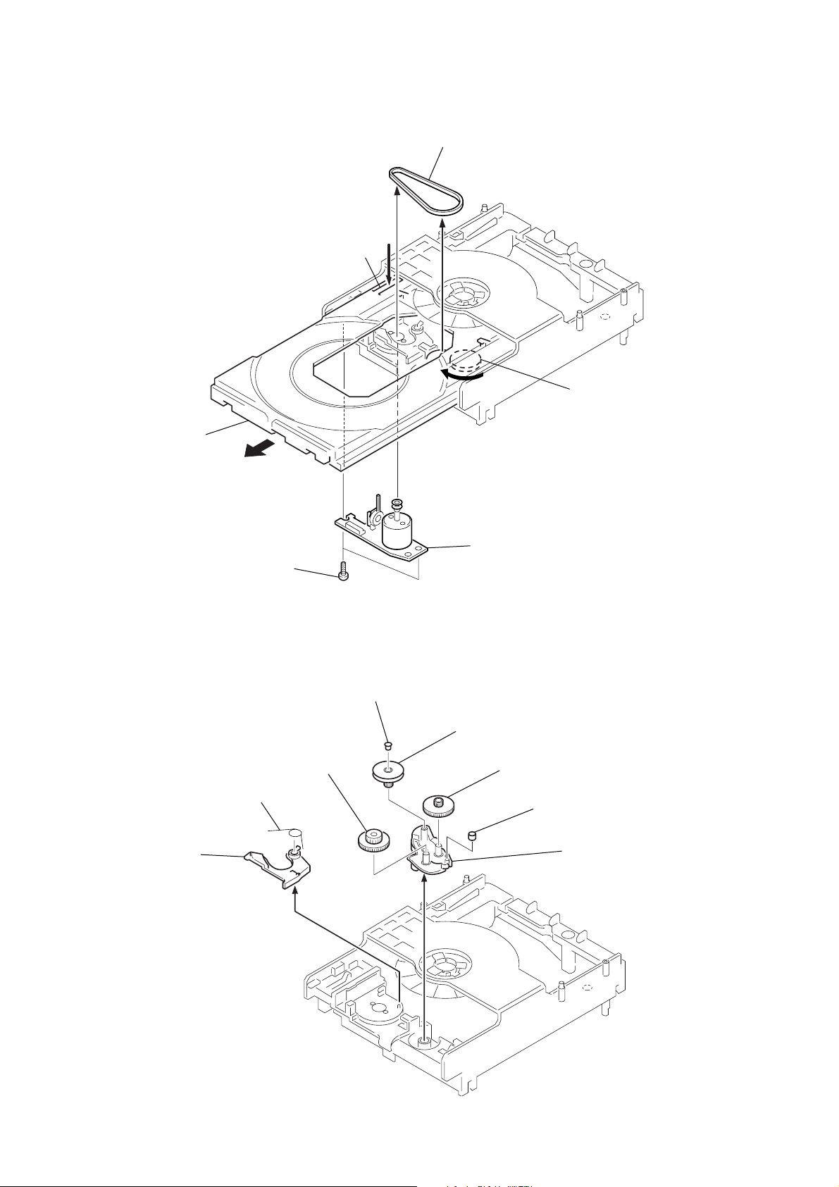
3-6. CD MECHANISM DECK (CDM55F-K6BD41A)
1
flexible flat cable (19core)
(CN101)
3
screw
(BTP3
×
8)
2
connector
(CN401)
HCD-DC1
4
CD mechanism deck (CDM55F-K6BD41A)
3-7. BASE UNIT (BU-K6BD41A)
2
base unit (BU-K6BD41A)
1
floating screw
(PTPWHM2.6)
9
HCD-DC1
3-8. LOADING MOTOR BOARD
B
2
belt (CDM55)
3
Pull the tray pushing B.
3-9. CAM (CDM55)
4
two screws
(BTP2.6
×
6)
6 gear (B)
3 spacer (55)
A
4 pulley (LDG)
1
5
LOADING MOTOR board
5 gear (A)
Rotate the gear(B) in
the direction of arrow
A
.
10
2 lever (SW)
1 torsion spring
7 roller
8 cam (CDM55)
SECTION 4
TEST MODE
HCD-DC1
[Cold Reset]
• The cold reset clears all data including preset data stored in the
RAM to initial conditions. Execute this mode when returning
the set to the customer.
Procedure:
1. Turn ON the power.
2. Press three buttons x (TAPE), x (CD), and
[TUNER/BAND] simultaneously.
3. The set is reset.
[Liquid Crystal Display All Lit Check Mode]
Procedure:
1. Set to standby state.
2. Press three buttons of x (TAPE), x (CD), and
[FUNCTION] simultaneously.
3. Liquid crystal display are all turned on.
4. To e xit from this mode, press the I/1 button to turn the power
OFF.
[Tape Deck Aging Mode]
This mode can be used for operation check of tape deck section.
Procedure:
1. Set a tape in the tape deck.
2. Set to standby state.
3. Press three buttons of x (TAPE), x (CD), and [+] (TUNING)
simultaneously.
4. The aging is executed in bellow sequence.
5. To exit from the aging mode, press the I/1 button to turn the
power OFF.
[CD Aging Mode]
This mode can be used for operation check of CD section.
Procedure:
1. Load a CD disc.
2. Set to standby state.
3. Press three buttons of x (TAPE), x (CD), and [--] ( TUNING)
simultaneously.
4. The aging is executed in bellow sequence.
5. To exit from the a ging mode, pr ess the I/1 button to turn the
power OFF.
Aging mode sequence:
Start
Open the disc tray
Close the disc tray
Play the last track
Aging mode sequence:
Start
FWD Play
REC pause for 3 seconds
FWD REC
Fast forward
REV Play
REC pause for 3 seconds
Shut off
1 minute
Shut off
3 minutes
Shut off
1 minute
REV REC
3 minutes
Rewind
Shut off
11
HCD-DC1
)
)
SECTION 5
ELECTRICAL ADJUSTMENT
DECK SECTION
Note: Confirm each contents of this section first of all. If the results are
not satisfied, do the adjustment.
0 dB=0.775 V
1. Demagnetize the record/playback head with a head
demagnetizer.
2. Do not use a magnetized screwdriver for the adjustments.
3. After the adjustments, apply suitable locking compound to the
parts adjust.
4. The adjustments should be performed with the rated power
supply voltage unless otherwise noted.
5. The adjustments should be performed in the order given in this
service manual. (As a general rule, playback circuit adjustment
should be completed before performing recording circuit
adjustment.)
6. The adjustments should be performed for both L-CH and RCH.
7. Switches and controls should be set as follows unless otherwise
specified.
• Test Tape
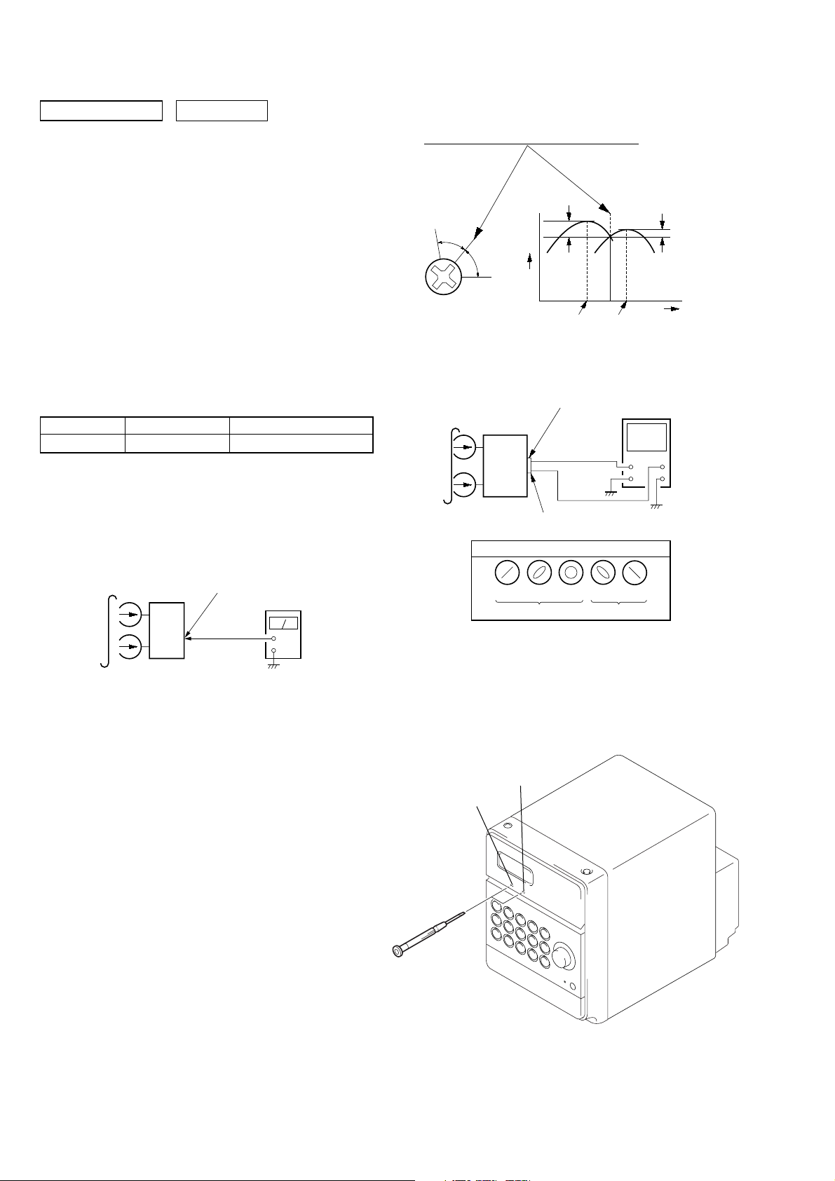
Tape Signal Used for
P-4-A100 10 kHz, –10 dB Azimuth Adjustment
Record/Playback Head Azimuth Adjustment
Procedure:
1. Mode: Playback
2. Turn the adjustment screw and check output peaks. If the peaks
do not match for L-CH and R-CH, turn the adjustment screw
so that outputs match within 1dB of peak.
Output
level
within
1 dB
L-CH
peak
R-CH
peak
within
1 dB
Screw
position
L-CH
peak
Screw
position
R-CH
peak
3. Mode: Playback
MAIN board
test tape
P-4-A100
(10 kHz, –10 dB)
set
SPEAKER terminals (SJ301
L-CH
R-CH
oscilloscope
V
H
test tape
P-4-A100
(10 kHz, –10 dB)
MAIN board
SPEAKER terminals (SJ301
L-CH, R-CH
level meter
set
waveform of oscilloscope
in phase 45° 90 ° 135° 180°
good
+
–
wrong
4. Repeat step 1 to 3 in playback (REV) mode.
5. After the adjustments, apply suitable locking compound to the
pats adjusted.
Adjustment Location:
reverse
forward
12
HCD-DC1
IC103
TP (RF)
TP (VC)
V
CD SECTION
Note:
1. CD Block is basically constructed to operate without
adjustment.
2. Use YEDS-18 disc (3-702-101-01) unless otherwise indicated.
3. Use an oscilloscope with more than 10 MΩ impedance.
4. Clean the object lens by an applicator with neutral detergent
when the signal level is low than specified value with the
following checks.
5. Check the focus bias check when optical block is replaced.
Focus Bias Check
oscilloscope
(DC range)
CD board
TP (RF)
TP (VC)
Procedure :
1. Connect oscilloscope to TP (RF) and TP (VC) on the CD board.
2. Press the I/1 button to turn the power on, and press the Z
(CD) button to open the CD disc tray.
3. Put disc (YEDS-18) in and press the u (CD) button to playback.
4. Confirm that oscilloscope waveform is as shown in the figure
below. (eye pattern)
A good eye pattern means that the diamond shape ( ) in the
center of the waveform can be clearly distinguished.
+
–
s
Checking Location:
– CD BOARD (Conductor Side) –
VOLT/DIV: 200 m
TIME/DIV: 500 ns
level:
1.2 ± 0.1 Vp-p
13

HCD-DC1
MEMO
14
SECTION 6
DIAGRAMS
6-1. BLOCK DIAGRAM – CD SERVO Section –
HCD-DC1
PICK-UP BLOCK
(KSS-213DCP)
DETECTOR
LASER DIODE
(TRACKING)
(FOCUS)
OPTICAL
7 D+5V
4
2
1
5
I-V AMP
10
6
LDPD
2-AXIS DEVICE
VCC
LD
PD
AUTOMATIC
POWER
CONTROL
Q101
M102
(SLED)
M101
(SPINDLE)
FILTER
54 56 53 55
ERROR
RF AMP
FOCUS/TRACKING ERROR AMP
A
5
B
6
C
7
D
8
F
10
FI-V AMP
E
11
EI-V AMP
LD
3
FOCUS/TRACKING COIL DRIVE,
SPINDLE/SLED MOTOR DRIVE
CH2OUTF
12
CH2OUTR
11
CH1OUTF
14
CH1OUTR
13
CH3OUTF
17
MM
MM
18
CH4OUTF
15
CH4OUTR
16
CH3OUTR
APC LD
AMP
APC PD
AMP
PD
4
IC103
RF
SUMMING
AMP
ERROR AMP
IC102
MOTOR
COIL
DRIVE
DRIVE
COIL
DRIVE
MOTOR
DRIVE
MOTOR
DRIVE
FOCUS
TRACKING
ERROR AMP
CH2 FIN
CH2RIN
CH1FIN
CH1RIN
CH3FIN
CH3RIN
CH4SIN
RF EQ
AMP
RFO
LD ON
HOLD SW
5
6
2
3
24
23
25
RFAC
16
FE
14
TE
13
22
21
41 39 4340
FE
TE
SE
RFDC
A/D
CONVERTER
TRDR
31
TFDR
30
FRDR
33
FFDR
32
SFDR
28
SRDR
29
PWM GENERATOR
FOCUS/TRACKING/SLED
ASYMMETRY
51
CORRECTION
ASYI
49
ASYO
48
SERVO DSP
FOCUS/TRACKING/SLED
SUBCODE
PROCESSOR
XLON
TO
SERVO
INTERFACE
IC101 (1/2)
FOK
MIRR/DFCT/FOK
DFCT
23 2224
FILI
PCO
FILO
CLTV
DIGITAL
PLL
CPU INTERFACE
SCOR
SENS
SQSO
DIGITAL SERVO
PROCESSOR
IC101 (2/2)
DETECTOR
MIRR
CORRECTOR
EFM
DEMODULATOR
SERVO AUTO
SEQUENCER
DATA
CLOK
XLAT
16k
RAM
SQCK
2576208114
DIGITAL SIGNAL PROCESSOR,
DIGITAL FILTER, D/A CONVERTER
IC101 (1/2)
D/A
INTERFACE
INTERNAL BUS
SERVO
INTERFACE
MIRR/DFCT/FOK DETECTOR
SSTP
IC101 (2/2)
SCLK
9 27
TO
S101
(LIMIT)
DIGITAL
SERIAL
IN
INTERFACE
DIGITAL
CLV
MDP
26
OUT
NOISE SHAPER
XRST
3
DIGITAL
FILTER
Q803
Q804
Q806
Q802
CD ON SWITCH
CLOCK
GENERATOR
TIMING
LOGIC
XTAL
16.9344MHz
Q802 – 808
VDD
515171
76
AIN1
AIN2
PWM
&
INTEGRATOR
XTAO
6766
X101
Q805
Q807
Q808
D OUT
AOUT1
AOUT2
60
70
77
• R-CH : R-ch is omitted due to same as L-ch.
• SIGNAL PATH
: CD PLAY (ANALOG)
: CD PLAY (DIGITAL OUT)
OPTICAL
TRANSCVER
IC321
BUFFER
LOUT1
LOUT2
OPTICAL
DIGITAL OUT (CD)
72
75
CD L IN
DATA
LATCH
SENS
SQSO
SQCK
XRST
HOLD
C SCOR
CLK
R-CH
A
(Page 16)
MUTE
MUTE
20
1515
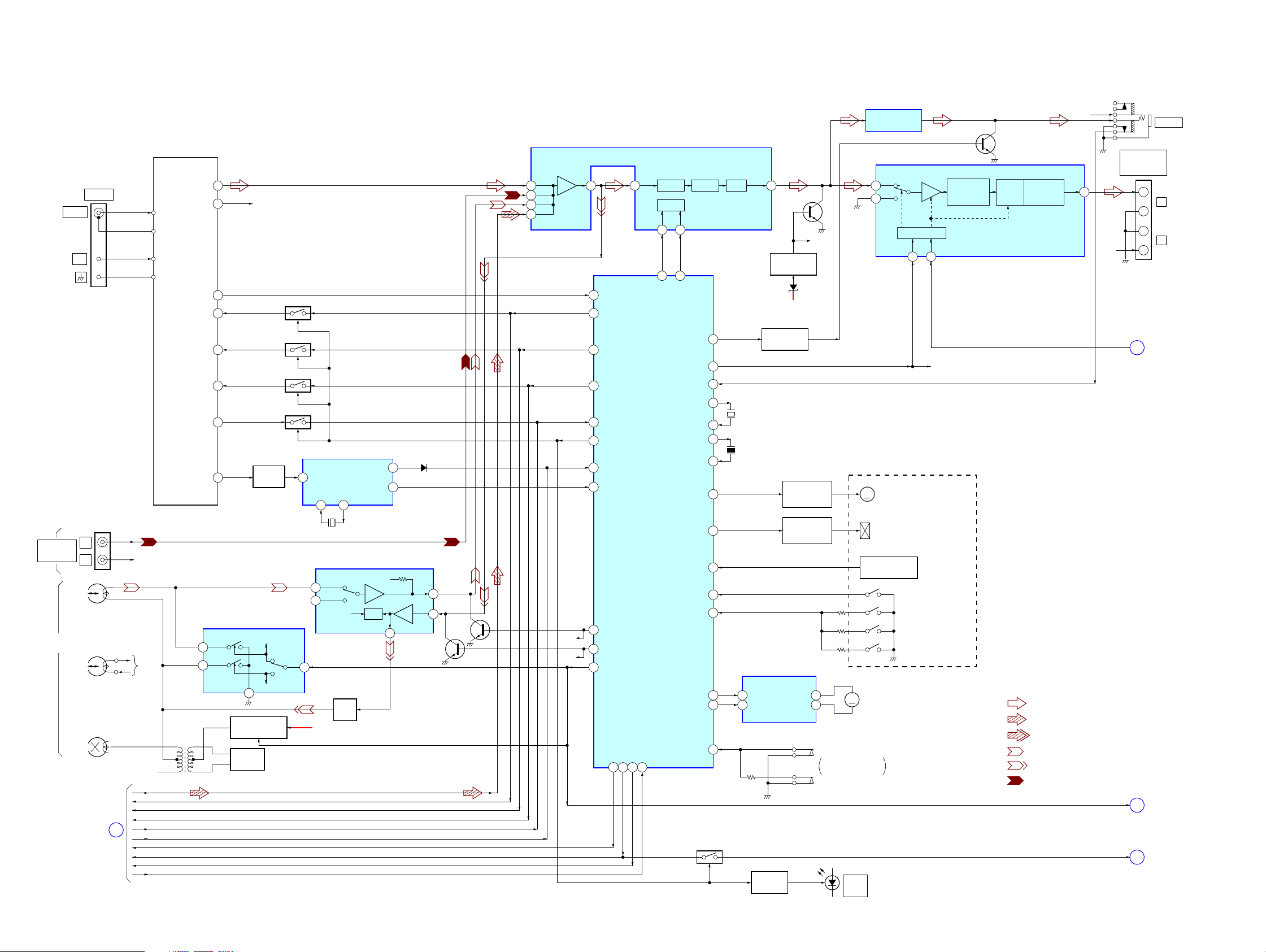
HCD-DC1
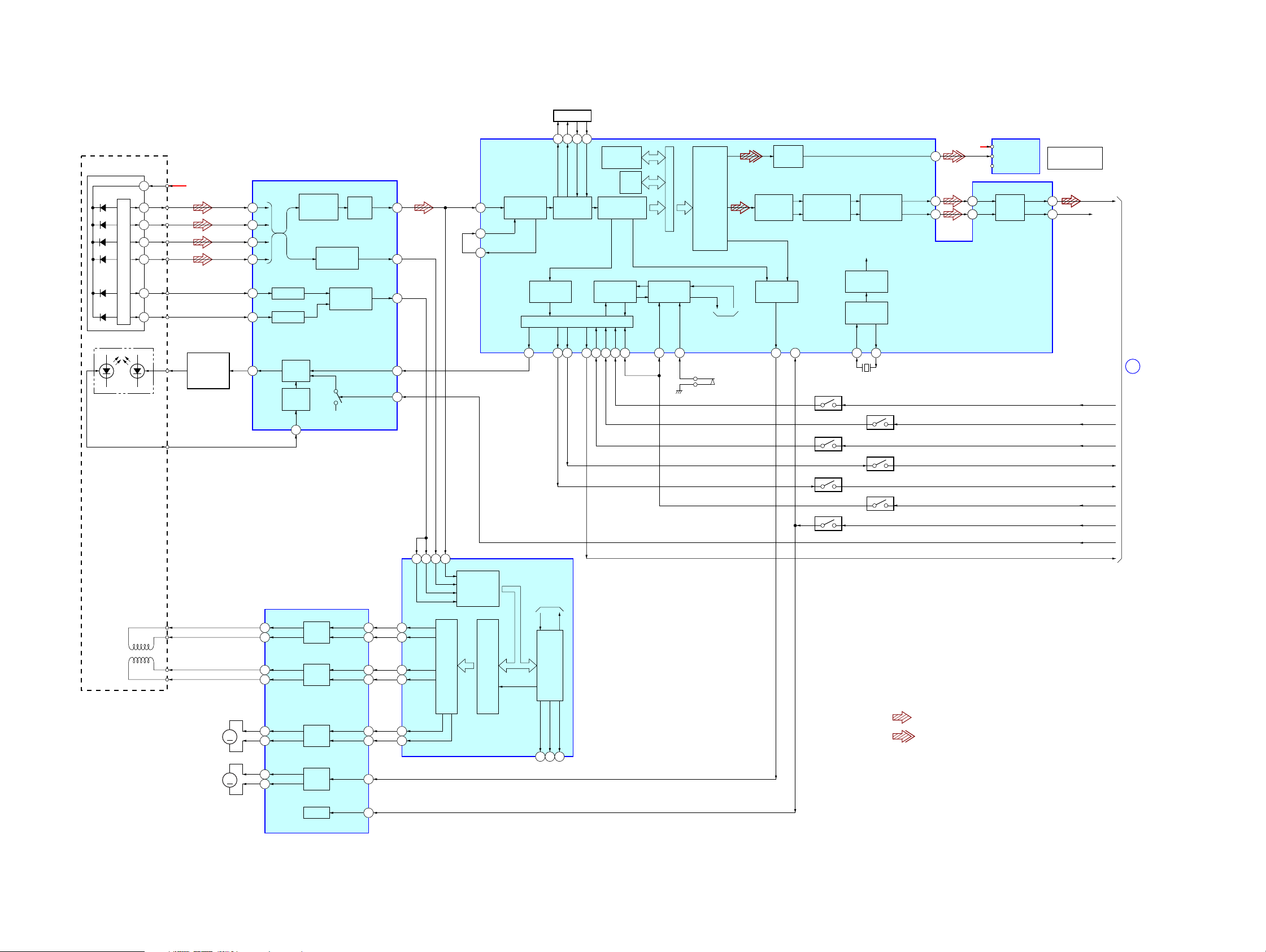
6-2. BLOCK DIAGRAM – MAIN Section –
ANENNA
FM75Ω
AM
AUDIO IN
MD (VIDEO)
HRPE901
(RECORD/PLAYBACK/ERASE)
L
R
L-CH
R-CH
(ERASE)
(Page 15)
SJ302
SJ301
SPEAKER
+
–
–
+
B
D
C
J301
PHONES
L
R
(Page 17)
(Page 17)
(Page 17)
OUT
R-CH
IMPEADANCE
USE 6 – 16Ω
14
R-CH
REG CON
REC/PB
FM ON
INPUT SELECT SWITCH,
MIX, TONE CONTROL,
ELECTRICAL VOLUME
TU1
TUNER PACK
LINE
OUT2
1
L-CH
2
FM ANT
ANT GND
AM ANT
ANT GND
R-CH
R-CH
CD L IN
DATA
CLK
LATCH
A
SENS
SQSO
SQCK
XRST
HOLD
C SCOR
R-CH R-CH
Q809 – 811, 813
TUNER ON/OFF
4
TUNED
9
DI
8
CK
10
CE
7
DO
3
FM DET MIX
REC/PB SWITCHING
IC402
(REC)
1
(PB)
3
2
BIAS
OSC
T401
REC BIAS SWITCH
Q402, 403
BIAS OSC
Q401
Q810
Q809
Q811
Q813
DET AMP
Q812
R-CH
R-CH
SWITCH
4.332MHz
(SW)
4
X803
4
X1 X0
13 14
B IN L
23
A IN L
24
B+
(+8V)
RDATA
RCLK
RDS DECODER
REC/PB AMP, EQ AMP
IC401
R-CH
R-CH
ALC
REC OUT L
T403
BIAS
TRAP
IC804
16
D806
2
16
PB L
20
REC
IN L
14
MUTING
Q407
MUTING
Q414
C2
6
A2
2
D2
8
E2
10
31 30 17
LINE
AMP
17
19
18
25
12
96 L-MUTE
R-CH
87 REC-MUTE
R-CH
95
IC323
TUNED
5
C-DATA/TU-DATA
C-CLK/TU-CLK
8
C-LATCH/TU-CE
SENS2/TU-COUNT
TU-ON
C-SQSO/
RDS-DATA
2
RDS-IN
SYSTEM CONTROLLER
IC801 (1/2)
REC/PB
C-SQCK
C-XRST/FM-ON
11 86 14 100
VOL2 OUT2
TREBLE
DATA CLK
14 15
88 28
HOLD
C-SCOR
LOGIC
SDA
AU-MUTE
AMP-MUTE
H/P CHECK
MOT-CON
SOL-CON
TAPE-END
TRAY-OPEN
TRAY-CLOSE
TRAY-SW
MIDDLE BASS
SCK
97
22
24
92
TX
93
TEX
40
XTAL1
39
EXTAL1
10
T-MODE
32
TC-SW
13
15
33
Q801
X802
32.768KHz
X801
4.19MHz
4
1
6
6
5
MUTING DRIVE
Q312, 313
LOADING
MOTOR DRIVE
IC320
INPUT2
INPUT1
LED DRIVE
Q854
MUTING
Q100
MUTING DRIVE
Q330
B+ (+8V)
CAPSTAN/REEL
MOTOR DRIVE
Q601, 602
TRIGGER
PLUNGER DRIVE
Q603, 604
OUT2
OUT1
R-CH
10
2
OPEN/CLOSE DETECT
HEADPHONE AMP
(TAPE DECK BLOCK)
MM
TAPE END DETECT
M901
MM
(LOADING)
SI
DISC TRAY
D853
TUNER
/BAND
IC324
IN+
3
4
IN–
STANDBY/MUTE
MUTE STBY
SENSOR
10 9
R-CH
MOS GAIN &
LEVEL SHIFT
ING STAGE
MUTING
Q815, 817
MOS
STAGE
SHORT
CIRCUIT
PROTECTION
POWER AMP
IC201
OUTPUT
• R-CH : R-ch is omitted due to same as L-ch.
• SIGNAL PATH
: TUNER
: CD PLAY (ANALOG OUT)
: CD PLAY (OPTICAL OUT)
: TAPE (PLAY)
: TAPE (RECORD)
: MD
1616
 Loading...