

Sony HCDCP-333 Service manual
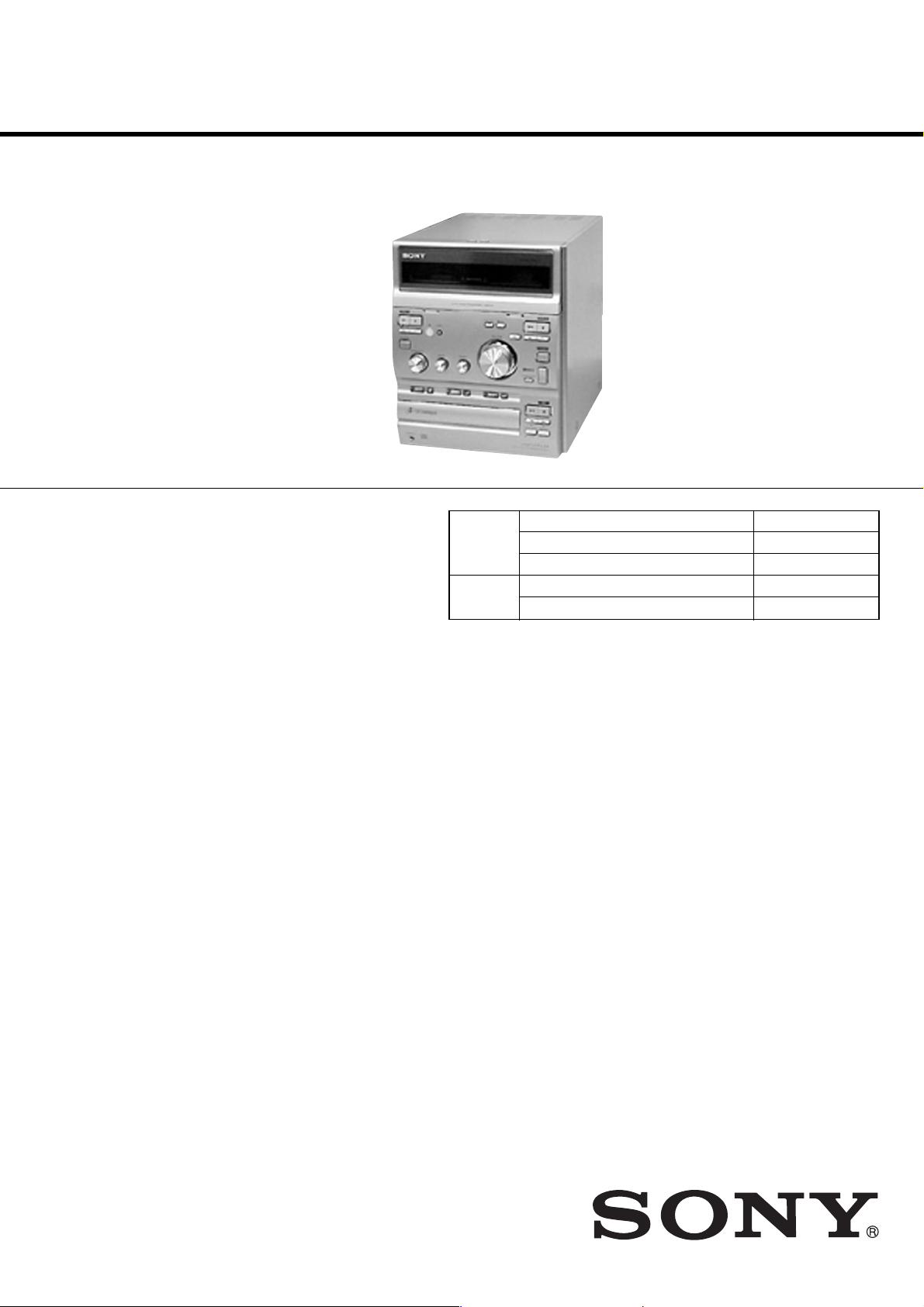
HCD-CP333
SERVICE MANUAL
Ver 1.1 2003. 11
• HCD-CP333 is the Amplifier, CD player,
Tape Deck and Tuner section in
CMT-CP333.
CD
Section
Tape deck
Section
US Model
Canadian Model
AEP Model
UK Model
E Model
Model Name Using Similar Mechanism HCD-CP300
CD Mechanism Type CDM63K-K6BD44
Optical Pick-up Type KSM-213D
Model Name Using Similar Mechanism HCD-CP300
Tape Transport Mechanism Type CMBL6Z511A
Amplifier section
For the U.S. model
AUDIO POWER SPECIFICATIONS
POWER OUTPUT AND TOTAL
HARMONIC DISTORTION:
With 6-ohm loads, both channels driven, from
120 - 10,000 Hz; rated 40 watts per channel
minimum RMS power, with no more than 10%
total harmonic distortion from 250 milliwatts to
rated output.
North American model
Continuous RMS power output (reference):
Total harmonic distortion less than 0.07% (6 ohms at
1 kHz, 32 W)
European model
DIN power output (rated): 32 + 32 W
Continuous RMS power output (reference):
Music power output (reference):
Other models
The following measured at 230 V AC, 60 Hz
DIN power output (rated): 30 + 30 W
40 + 40 W
(6 ohms at 1 kHz, 10%
THD)
(6 ohms at 1 kHz, DIN)
40 + 40 W
(6 ohms at 1 kHz, 10%
THD)
100 + 100 W
(6 ohms at 1 kHz, DIN)
SPECIFICATIONS
Continuous RMS power output (reference):
The following measured at 220 V AC, 60 Hz
DIN power output (rated): 27 + 27 W
Continuous RMS power output (reference):
Inputs
AUDIO IN MD (VIDEO) (phono jacks):
Outputs
CD DIGITAL OUT OPTICAL:
PHONES:
SPEAKER:
CD player section
System
38 + 38 W
(6 ohms at 1 kHz, 10%
THD)
(6 ohms at 1 kHz, DIN)
35 + 35 W
(6 ohms at 1 kHz, 10%
THD)
Sensitivity 500/250 mV,
impedance 47 kilohms
Optical
Accepts headphones with
an impedance of 8 ohms
or more
6 ohms
Compact disc and digital
audio system
MICRO HI-FI COMPONENT SYSTEM
Laser Semiconductor laser
Wavelength 780 - 790 nm
Frequency response 20 Hz - 20 kHz (±0.5 dB)
Tape player section
Recording system 4-track 2-channel stereo
Frequency response 50 - 13,000 Hz (±3 dB),
Tuner section
FM stereo, FM/AM superheterodyne tuner
FM tuner section
Tuning range
North American model: 87.5 - 108.0 MHz
Other models: 87.5 - 108.0 MHz
Antenna FM wire antenna
Antenna terminals 75 ohm unbalanced
Intermediate frequency 10.7 MHz
(λ = 780 nm)
Emission
duration: continuous
using a Sony TYPE I
cassette
(100-kHz step)
(50-kHz step)
— Continued on next page —
9-877-051-02
2003K16-1
© 2003.11
Sony Corporation
Home Audio Company
Published by Sony Engineering Corporation

HCD-CP333
Ver 1.1 2003.11
AM tuner section
Tuning range
North American model: 530 - 1,710 kHz
European model: 531 - 1,602 kHz
Other models: 530 - 1,710 kHz
Antenna AM loop antenna, external
Intermediate frequency 450 kHz
General
Power requirements
North American model: 120 V AC, 60 Hz
European model: 230 V AC, 50/60 Hz
Other models: 110 - 120 V or 220 -
Power consumption
European model
Other models: 70 W
Dimensions (w/h/d) Approx. 225 × 273 ×
Mass Approx. 7.3 kg
•Design and specifications are subject to change without notice.
(with the tuning interval
set at 10 kHz)
531 - 1,710 kHz
(with the tuning interval
set at 9 kHz)
(with the tuning interval
set at 9 kHz)
(with the tuning interval
set at 10 kHz)
531 - 1,602 kHz
(with the tuning interval
set at 9 kHz)
antenna terminal
240 V AC , 50/60 Hz
Adjustable with voltage
selector
70 W
0.4 W (at the power
saving mode)
385 mm incl. projecting
parts and controls
TABLE OF CONTENTS
1. SERVICING NOTES························································· 4
2. GENERAL············································································ 5
3. DISASSEMBLY··································································7
3-1. Cover (Upper) ·································································8
3-2. Front Panel Section························································· 8
3-3. Tape Mechanism Deck-1 ················································9
3-4. Tape Mechanism Deck-2 ················································9
3-5. LED Board, CONTROL Board ···································· 10
3-6. Back Panel Sub Assy, J ACK Board ······························ 10
3-7. MAIN Board ·································································11
3-8. POWER Board······························································ 11
3-9. CD Mechanism Deck (CDM63K-K6BD44) ················ 12
3-10.CD Board ······································································ 12
3-11.Base Unit (BU-K6BD44) ·············································13
3-12.Tray Assy ······································································ 13
3-13.Silder (Loading)···························································· 14
3-14.TRAY SENSOR Board, MOTOR Board······················ 14
3-15.IN OUT SW Board ······················································· 15
3-16.Stocker Assy ································································· 15
3-17.CD Base Unit Assy, DISC SENSOR Board ················· 16
4. TEST MODE ······································································ 17
5. ELECTRICAL ADJUSTMENTS································· 18
6. DIAGRAMS ·······································································20
6-1. Note For Printed Wiring Boards And Schematic
Diagrams······································································· 20
6-2. Block Diagrams ···························································· 21
6-3. Circuit Boards Location················································ 23
6-4. Printed Wiring Board – CD Board – ···························24
6-5. Schematic Diagram - CD Board -································· 25
6-6. Printed Wiring Board – TC Board –····························· 26
6-7. Schematic Diagram – TC Board – ································ 27
6-8. Printed Wiring Board – MAIN Board – ······················· 28
6-9. Schematic Diagram – MAIN Board (1/3) – ················· 29
6-10.Schematic Diagram – MAIN Board (2/3) – ·················30
6-11.Schematic Diagram – MAIN Board (3/3) – ·················31
6-12.Printed Wiring Board – CONTROL Section – ············· 32
6-13.Schematic Diagram – CONTROL Section –················ 33
6-14.Printed Wiring Board – DRIVER Section –················· 34
6-15.Schematic Diagram – DRIVER Section –···················· 35
6-16.Printed Wiring Board – POWER Board – ···················· 36
6-17.Schematic Diagram – POWER Board – ·······················37
6-18.Printed Wiring Board – LCD Section –························ 38
6-19.Schematic Diagram – LCD Section –··························· 38
6-20.IC Pin Function Description ········································· 39
6-21.IC Block Diagrams ······················································· 41
7. EXPLODED VIEWS························································ 44
7-1. Cover Section································································ 44
7-2. Front Panel Section······················································· 45
7-3. Chassis Section ····························································· 46
7-4. CD Mechanism Deck-1 ················································47
7-5. CD Mechanism Deck-2 ················································48
7-6. KSM-213D ··································································· 49
8. ELECTRICAL PARTS LIST········································· 50
2
HCD-CP333
1.5 k
Ω
0.15 µF
AC
voltmeter
(0.75 V)
To Exposed Metal
Parts on Set
Earth Ground
Notes on chip component replacement
•Never reuse a disconnected chip component.
• Notice that the minus side of a tantalum capacitor may be damaged by heat.
Flexible Circuit Board Repairing
•Keep the temperature of the soldering iron around 270 ˚C during repairing.
• Do not touch the soldering iron on the same conductor of the
circuit board (within 3 times).
• Be careful not to apply force on the conductor when soldering
or unsoldering.
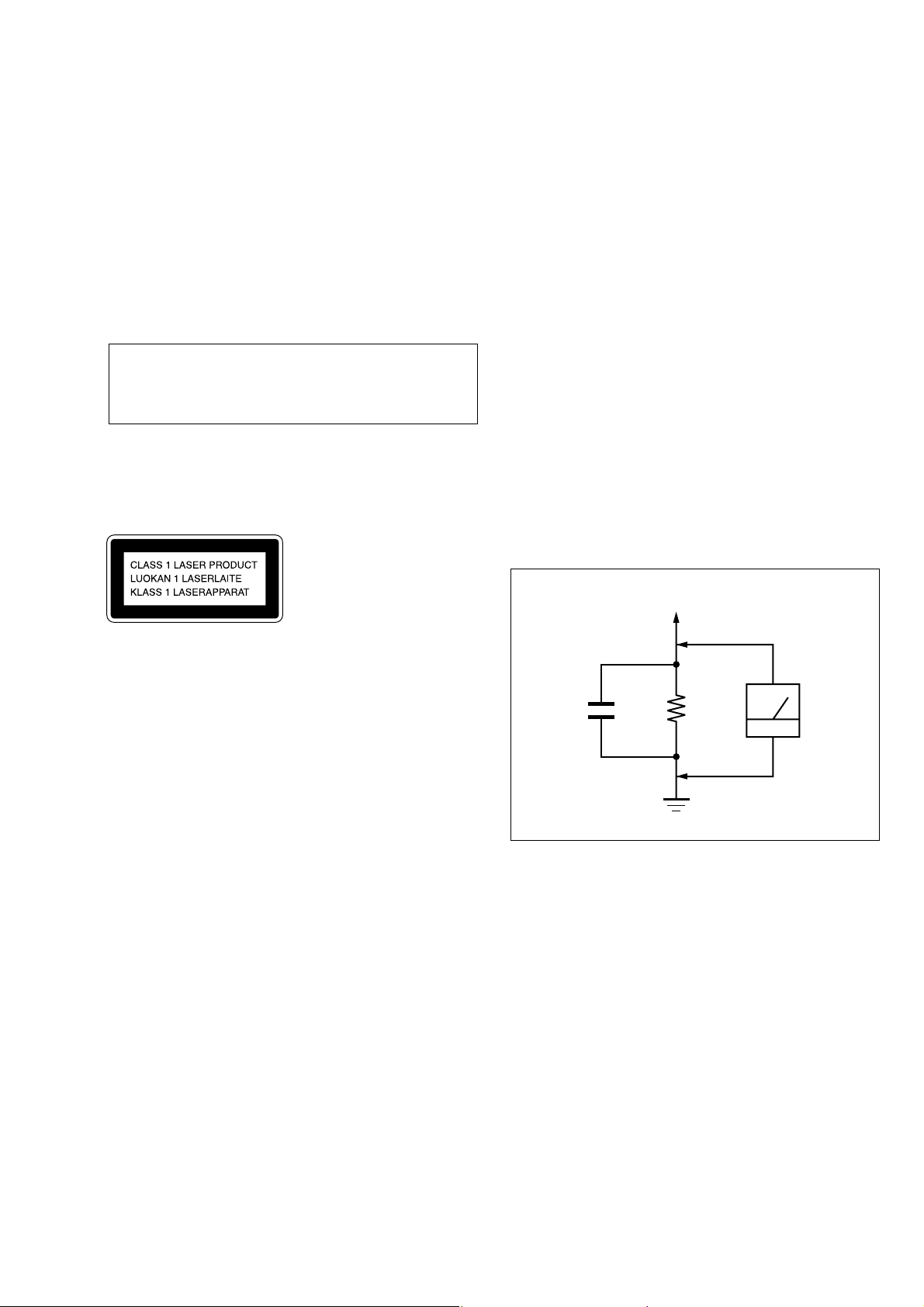
CAUTION
Use of controls or adjustments or performance of procedures
other than those specified herein may result in hazardous
radiation exposure.
This appliance is classified as a CLASS 1 LASER product.
The CLASS 1 LASER PRODUCT MARKING is located on
the rear exterior.
SAFETY CHECK-OUT
After correcting the original service problem, perform the following
safety check before releasing the set to the customer:
Check the antenna terminals, metal trim, “metallized” knobs, screws,
and all other exposed metal parts for AC leakage.
Check leakage as described below.
LEAKAGE TEST
The AC leakage from any exposed metal part to earth ground and
from all exposed metal parts to any exposed metal part having a
return to chassis, must not exceed 0.5 mA (500 microamperes.).
Leakage current can be measured by any one of three methods.
1. A commercial leakage tester, such as the Simpson 229 or RCA
WT-540A. Follow the manufacturers’ instructions to use these
instruments.
2. A battery-operated AC milliammeter. The Data Precision 245
digital multimeter is suitable for this job.
3. Measuring the voltage drop across a resistor by means of a V OM
or battery-operated A C voltmeter . The “limit” indica tion is 0.75
V, so analog meters must have an accurate low-voltage scale.
The Simpson 250 and Sanwa SH-63Trd are examples of a
passive V OM that is suitable. Nearly all battery operated digital
multimeters that have a 2 V A C range are suitable. (See Fig. A)
Laser component in this product is capable of emitting radiation
exceeding the limit for Class 1.
Fig. A. Using an AC voltmeter to check AC leakage.
SAFETY-RELATED COMPONENT WARNING!!
COMPONENTS IDENTIFIED BY MARK 0 OR DOTTED LINE WITH
MARK 0 ON THE SCHEMATIC DIAGRAMS AND IN THE PARTS
LIST ARE CRITICAL TO SAFE OPERATION. REPLACE THESE
COMPONENTS WITH SONY PARTS WHOSE PART NUMBERS
APPEAR AS SHOWN IN THIS MANUAL OR IN SUPPLEMENTS
PUBLISHED BY SONY .
ATTENTION AU COMPOSANT AYANT RAPPORT
À LA SÉCURITÉ!
LES COMPOSANTS IDENTIFÉS P AR UNE MARQUE 0 SUR LES
DIAGRAMMES SCHÉMA TIQUES ET LA LISTE DES PIÈCES SONT
CRITIQUES POUR LA SÉCURITÉ DE FONCTIONNEMENT. NE
REMPLACER CES COMPOSANTS QUE PAR DES PIÈSES SONY
DONT LES NUMÉROS SONT DONNÉS DANS CE MANUEL OU
DANS LES SUPPÉMENTS PUBLIÉS PAR SONY.
3
HCD-CP333
SECTION 1
SERVICING NOTES
NOTES ON HANDLING THE OPTICAL PICK-UP
BLOCK OR BASE UNIT
The laser diode in the optical pick-up block may suffer electrostatic
break-down because of the potential difference generated by the
charged electrostatic load, etc. on clothing and the human body.
During repair, pay attention to electrostatic break-down and also
use the procedure in the printed matter which is included in the
repair parts.
The flexible board is easily damaged and should be handled with
care.
NOTES ON LASER DIODE EMISSION CHECK
The laser beam on this model is concentrated so as to be focused on
the disc reflective surface by the objective lens in the optical pickup block. Therefore, when checking the laser diode emission,
observe from more than 30 cm away from the objective lens.
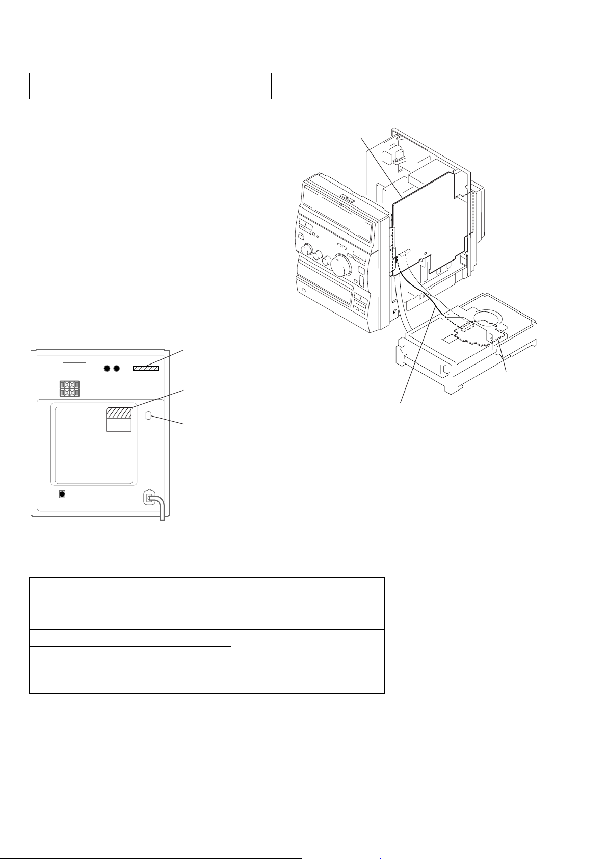
MODEL IDENTIFICATION
— BACK PANEL —
Parts No.
SERVICE POSTION
In checking the CD block, prepare jig (extension cable J-2501-011B).
MAIN board
Power Voltage Indication
VOLTAGE SELECTOR
Switch
MODEL PARTS No.
AEP model 4-233-470-3s
UK model 4-233-470-3s
US model 4-233-470-4s
Canadian model 4-233-470-4s
E model 4-233-470-5s
CD board
Connect jig (extension cable J-2501-011-B)
to the MAIN board (CN304) and CD board (CN101).
POWER V OLTA GE INDICA TION
AC:230V 50/60Hz 70W
AC:120V 60Hz 70W
AC:110-120/220-240V
50/60Hz 70W
4
Main unit
ef
ed
es
ea
e;
SECTION 2
GENERAL
1234 5~6987q;
ZZ
z
Y
xMx
X
m
M
?/1
ZZZ
m
M
ux
.
>
m
M
HCD-CP333
This section is extracted
from instruction manual.
qa
qs
qd
qf
qg
qh
qj
qk
1 DISC indicator wa
BASS ea
CD 1 wd
CD 1 Z wf
CD 2 wg
CD 2 Z wh
CD 3 wj
CD 3 Z wk
CD SYNC 7
CD u ws
CD x qj
CD ./> qk
CD m/M qk
wl
DECK A EJECT Z 5
DECK B EJECT Z 6
DSG 4
FUNCTION es
PHONES jack
PLAY MODE
Remote sensor
REPEAT ql
TAPE A N 1
TAPE B Y 0
TAPE A x 2
TAPE B x qa
wd~wk ws w;wa ql
wl
w;
3
TAPE A m/M ef
TAPE B m/M qs
TAPE REC z 8
TAPE X 9
TREBLE e;
TUNER BAND qd
TUNING MODE qf
TUNING +/– qg
VOLUME qh
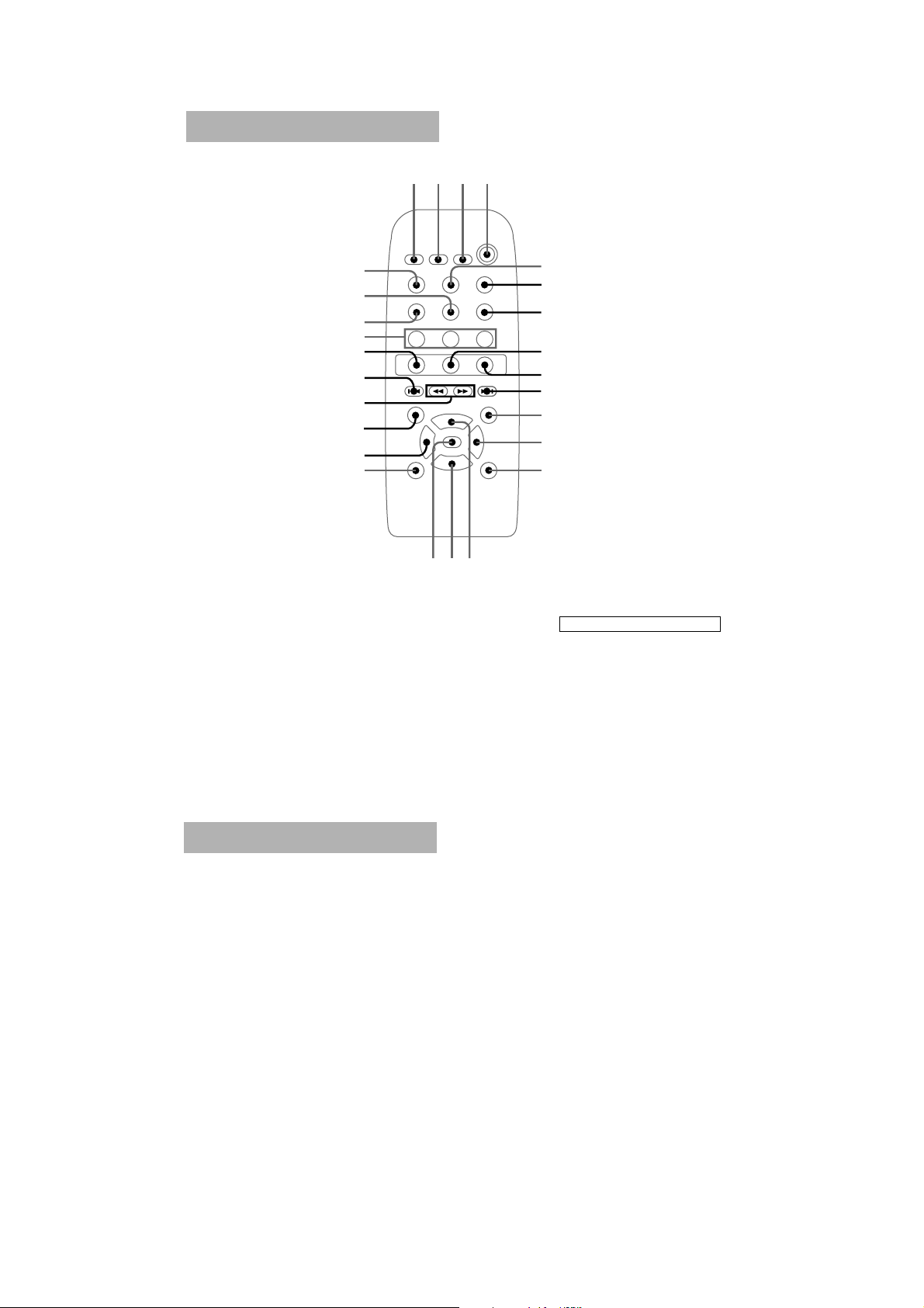
BUTTON DESCRIPTIONS
@/1 (power) ed
5
HCD-CP333
Remote Control
BASS/TREBLE ql
CD wj
DIRECTION qj
DISC1 wf
DISC2 wg
DISC3 wh
DISPLAY qs
DSG qa
ENTER qh
FUNCTION 5
MEMORY qk
wl
wk
wj
wf~wh
wd
ws
w;~wa
ql
qk
qj
123
NX x
qgqfqh
PLAY MODE wl
SLEEP 1
STEREO/MONO qd
TAPE A/B wk
TIMER SELECT 2
TIMER SET 3
TUNER/BAND 7
TUNING MODE 6
VOL + qf
VOL – qg
4
?/1
5
6
7
8
9
q;
qa
qs
qd
BUTTON DESCRIPTIONS
N wd
X 8
x 9
. ws
> 0
m w;
M wa
@/1 (power) 4
Setting the time
1
Turn on the system.
2
Press TIMER SET on the remote.
If you are setting the clock for the first time,
go to step 5.
3
Press ./> on the remote
repeatedly until “CLOCK” appears in
the display.
4
Press ENTER on the remote.
The hour indication flashes.
5
Press ./> on the remote
repeatedly to set the hour.
6
Press ENTER on the remote.
The minute indication flashes.
7
Press ./> on the remote
repeatedly to set the minute.
8
Press ENTER on the remote.
The clock will begin operating.
To reset the system clock
Start over from step 1.
6
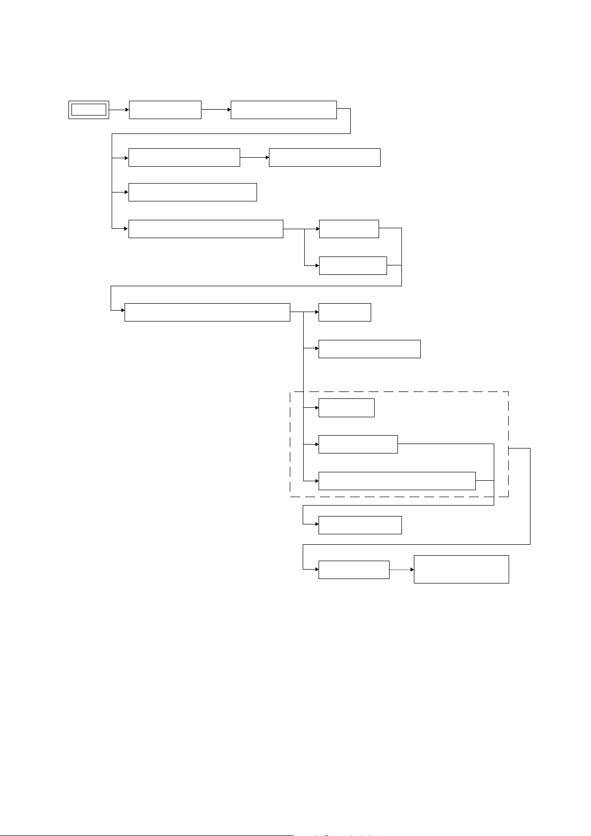
SECTION 3
DISASSEMBLY
• The equipment can be removed using the following procedure.
HCD-CP333
Ver 1.1 2003.11
SET
COVER (UPPER)
TAPE MECHANISM DECK-1 TAPE MECHANISM DECK-2
LED BOARD, CONTROL BOARD
BACK PANEL SUB ASSY, JACK BOARD
CD MECHANISM DECK (CDM63K-K6BD44)
FRONT PANEL SECTION
MAIN BOARD
POWER BOARD
CD BOARD
BASE UNIT (BU-K6BD44)
In order to remove stocker assy,
please remove tray assy, slider (loading) and tray sensor board.
TRAY ASSY
SLIDER (LOADING)
TRAY SENSOR BOARD, MOTOR BOARD
IN OUT SW BOARD
STOCKER ASSY
CD BASE UNIT ASSY,
DISC SENSOR BOARD
7
HCD-CP333
s
Note : Follow the disassembly procedure in the numerical order given.
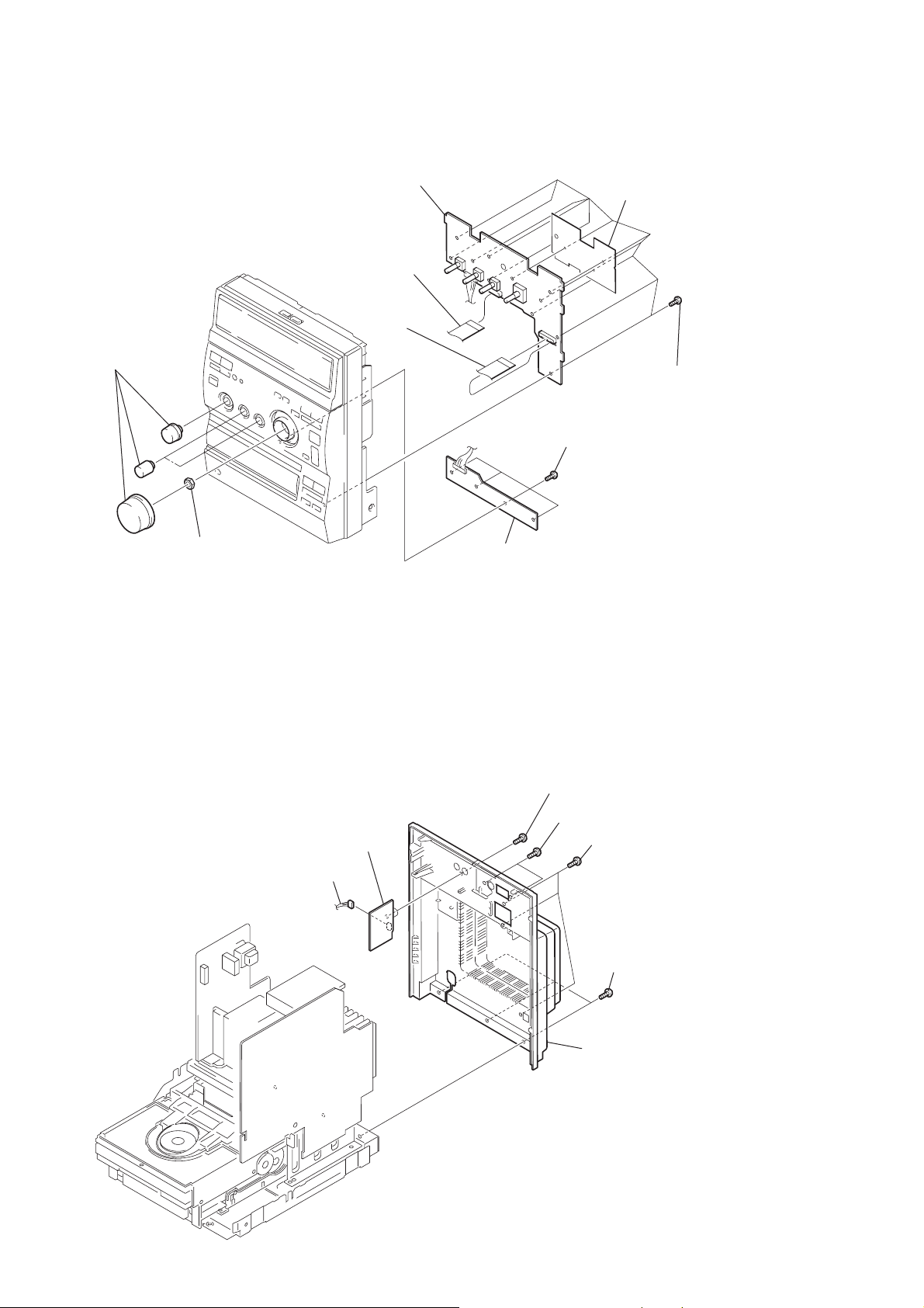
3-1. Cover (Upper)
4 cover (upper)
1 s
ix screws (+BTP 3
×
8)
3 two case
screws
3-2. Front Panel Section
7 w
ire (flat type) 15p (CN805)
8 w
ire (flat type) 17p (CN806)
2 two case
screw
qs s
crew (+KTP 3
qd
front panel section
6 w
ire (flat type) 17p (CN801)
5 w
ire (flat type) 21p (CN803)
2 c
onnector 2p (CN810)
1 c
onnector 2p (CN809)
3 w
ire (flat type) 11p (CN303)
4 w
ire (flat type) 11p (CN302)
9 c
onnector 4p (CN307)
×
6)
q; t
wo screws (+BTP 3
×
8)
qa s
crew (+KTP 3
×
6)
8
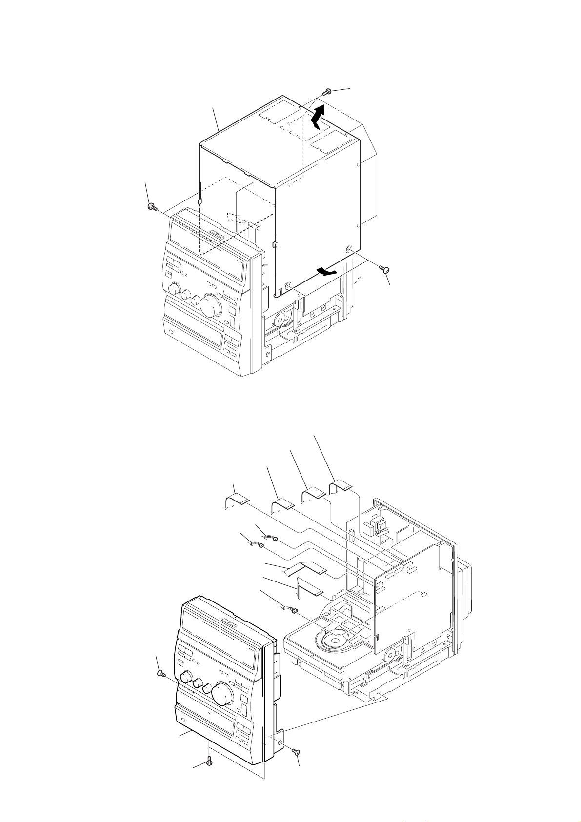
3-3. Tape Mechanism Deck-1
)
k
4
3
6 t
ape machanism deck
5
1 two
screws (+BVTP 3
×
8)
2 t
hree screws (+BVTP 3
HCD-CP333
×
8
3-4. Tape Mechanism Deck-2
qf t
wo screws (+BVTTWH tapping)
qa t
hree screws (+BVTP tapping)
3 c
assette holder (A)
sub assy
4 s
pring (cassette A)
1 c
assette holder (B) sub assy
2 s
pring (casstte B)
qg t
wo dampers
qd w
ire (flat type) 11p
qh t
ape machanism dec
qs b
racket (MD)
7 w
ire (flat type) 11p
(CN401)
q;
TC board
9
Remove solderings.
8 t
wo screws (+BVTP tapping)
5 s
crew (+BTP 3
6 s
hield case (TC)
×
8)
9
HCD-CP333
)
)
3-5. LED Board, CONTROL Board
1
four knobs
9
CONTROL board
7
w
ire (flat type)
15p (CN807)
8
w
ire (flat type)
17p (CN808)
3
four
6
5
eleven
screws (IT3B 2.6
shield sheet
screws (IT3B 2.6
×
8)
×
8
2
hexagon nut
3-6. Back Panel Sub Assy, JACK Board
6 JACK
1 c
onnector 3p (CN305)
board
4
LED board
5 s
crew (+BTP 3
4 t
wo screws (+BTP 3
3 t
hree screws (+BTP 3
2 t
×
8)
×
8)
×
hree screws (+BTP 3
8)
×
8
10
7 b
ack panel assy
3-7. MAIN Board
1 c
onnector 9p (CN902)
5 s
crew (+BVTP 3
HCD-CP333
×
12)
3-8. POWER Board
2 c
onnector 12p (CN313)
5
POWER board
3 w
ire (flat type) 21p (CN304)
4 s
crew (+BVTP 3
4 four
screws (+BVTP 4
3 c
onnector 2p (CN901)
6
MAIN board
×
×
8)
8)
2 c
onnector 9p (CN902)
1
earth plate
11
HCD-CP333
)
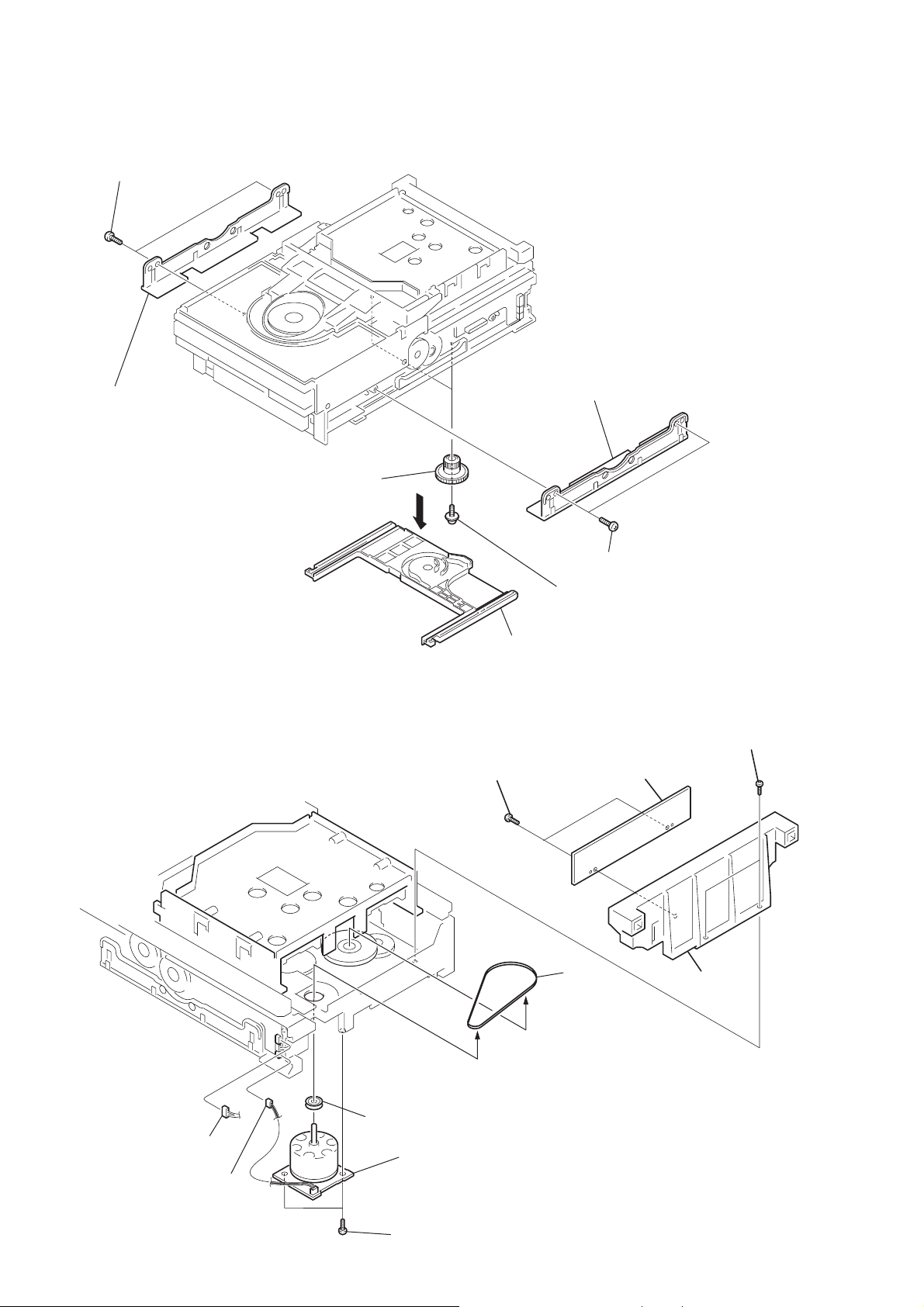
3-9. CD Mechanism Deck (CDM63K-K6BD44)
q;
CD machanism deck (CDM63K-K6BD44)
2 s
1 t
wo screws (+KTP 3
crew (+BVTP 3
×
×
8)
8)
3 two
screws
(+BVTP 3
×
5 t
wo screws (+BVTP 3
7 c
onnector 12p (CN701)
8)
6 w
ire (flat type)
21p (CN304)
8
cover (changer), MAIN board
×
8
4 b
racket (retainer)
3-10. CD Board
2
4
w
ire (flat type) 21p (CN101)
Remove solder (four portions ).
9 f
our screws (+BTP 3
1
(+BTP 2.6
screw
HARNESS PROCESSING
×
8)
×
6)
5
CD board
3
w
ire (parallel) 16p (CN102)
12
)
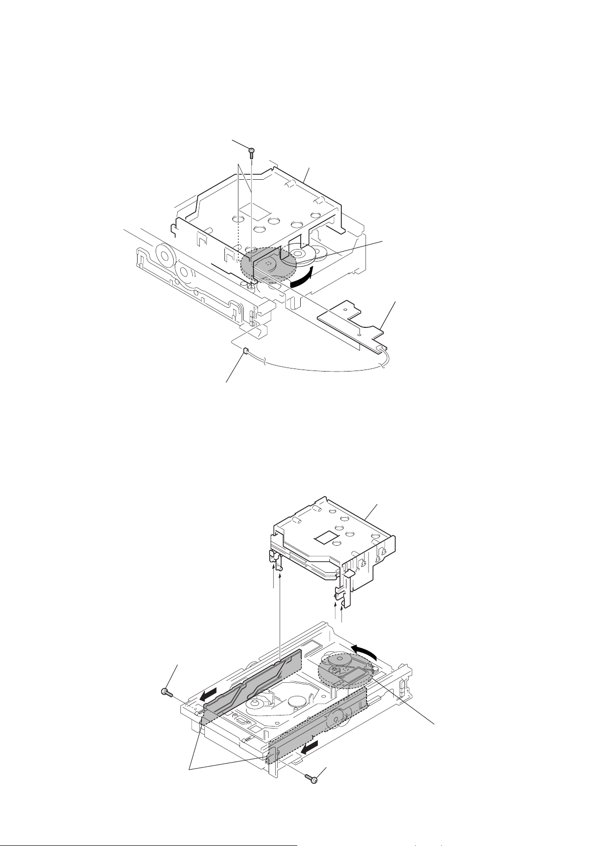
3-11. Base Unit (BU-K6BD44)
5 t
wo screws (IT3B 2.6
6 two stoppers (BU)
7 two
coil springs (insulator)
8 two i
nsulators
×
HCD-CP333
3 c
8)
oil spring (insulator)
4 i
nsulator
2 t
wo screws (+PTPWH 2.6
1 s
crew, froating
3 c
oil spring (insulator)
4 i
nsulator
ase unit
9 b
×
6
3-12. Tray Assy
1 t
wo screws (+BTTP M2.6)
tray assy
5
3 three bosses
4
rack (center)
2 t
wo screws (+BTTP M2.6)
3 three bosses
13
HCD-CP333
3-13. Silder (Loading)
3 t
wo screws
(+BTTP M2.6)
4 b
racket (retainer)
7 t
wo gears (slider)
2 b
racket (retainer)
3-14. TRAY SENSOR Board, MOTOR Board
4 t
wo screws (+BTTP M2.6)
8
slider (loading)
1 t
wo screws (+BTTP M2.6)
6 t
wo screws (+PTPWH M2.6)
2 t
wo screws (+BTTP M2.6)
5 TRAY SENSOR
7 b
elt
3 h
board
older (sensor)
14
1 c
onnector 5p (CN703)
6 c
onnector 2p (CN702)
9 p
ulley (motor)
8 t
q; m
otor board
wo screws (+BTTP M2.6)
3-15. IN OUT SW Board
2
t
wo screws (+BTTP M2.6)
stocker assy
1
Rotate the cam,
and up the stocker assy at the full.
4
IN OUT SW board
HCD-CP333
3
3-16. Stocker Assy
2 s
c
onnector 2p (CN704)
crew (+BTTP M2.6)
5 st
ocker assy
4
Slide the slider (BU.L),
slider (BU.R) in the direction of
arrow
A
at the full.
A
A
1 s
crew (+BTTP M2.6)
3
Rotate the cam,
and up the stocker assy at the full.
15
HCD-CP333
)
Ver 1.1 2003.11
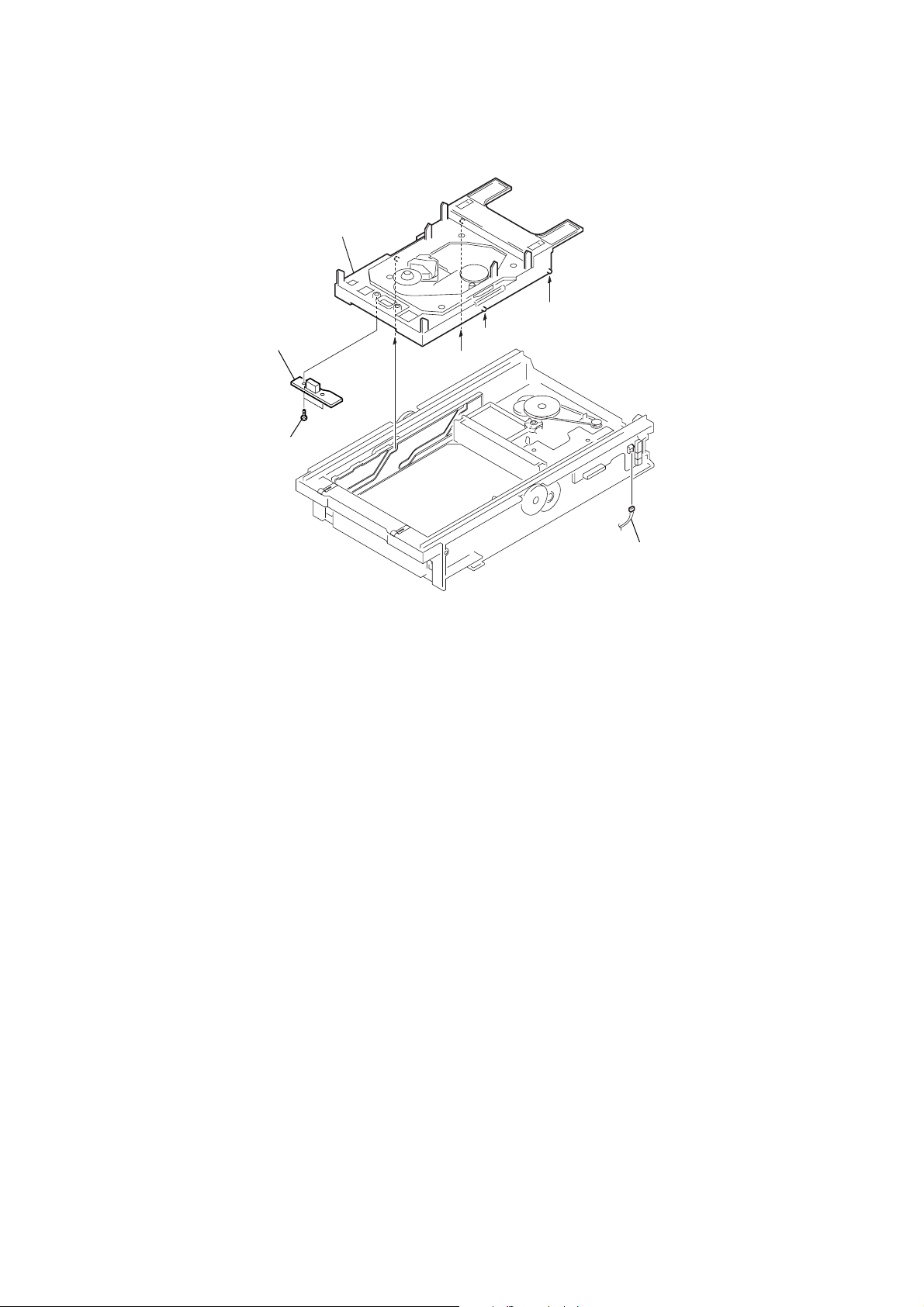
3-17. CD Base Unit Assy, DISC SENSOR Board
2
CD base unit assy
4
DISC SENSOR board
3
two screws (BTTP M2.6)
1
c
onnector 3p (CN705
16

SECTION 4
TEST MODE
HCD-CP333
[CD Ship Mode]
•This mode moves the optical pick-up to the position durable to
vibration. Use this mode when returning the set to the customer
after repair.
Procedure:
1. Press the ?/1 button to turn the set ON.
2. Press three buttons x (TAPE A), x (CD), and Z (CD1)
simultaneously.
3. After the “STANDBY” display blinks six times, a message
“LOCK” is displayed on the liquid crystal display, and the CD
ship mode is set.
[GC Test Mode]
•This mode is used to check the software version, liquid crystal
display and keyboard.
Procedure:
1. Press three buttons x (TAPE A), x (CD) and ?/1 simul-
taneously.
2. Segments of the liquid crystal display are all turned on.
3. When you want to enter the software version display mode,
press the CD 1 button . The model number and destination are
displayed.
4. Each time the CD 1 button is pressed, the display changes
starting from MC version, GC version, CD version, CDD
version, CDMA version, CDMB version, BDA version, BDB
version , ST version, TA version, TM version, TC version and
MD version in this order.
5. Press the CD 2 button, and the key check mode is activated.
6. In the key check mode, “K 0 J 0 V 0” is displayed. Each time
a button is pressed, “K 0” value increases. However, once a
button is pressed, it is no longer taken into account.
“V 0” value increases like 1, 2, 3 ... if rotating the VOLUME
knob clockwise, or it decreases like 0, 9, 8 ... if rotating
counterclockwise.
“J0” value increases if rotating the FUNCTION , BASS or
TREBLE knob clockwise, or it decreases if rotating
counterclockwise.
7. T o e xit from this mode, press three b uttons in the same manner
as step 1, or disconnect the power cord.
[CD Ship (Memory Clear) Mode]
• Set the CD ship mode and set the default setup when shipped
from the factory at the next AC power on.
Procedure:
1. Press the ?/1 button to turn the set ON.
2. Select the function “CD ”.
3. Press three buttons x (TAPE A), x (CD), and Z (CD1)
simultaneously.
4. After the “STANDBY” display blinks six times, a message
“LOCK” is displayed on the liquid crystal display, and the CD
ship mode is set.
17
HCD-CP333
)
)
SECTION 5
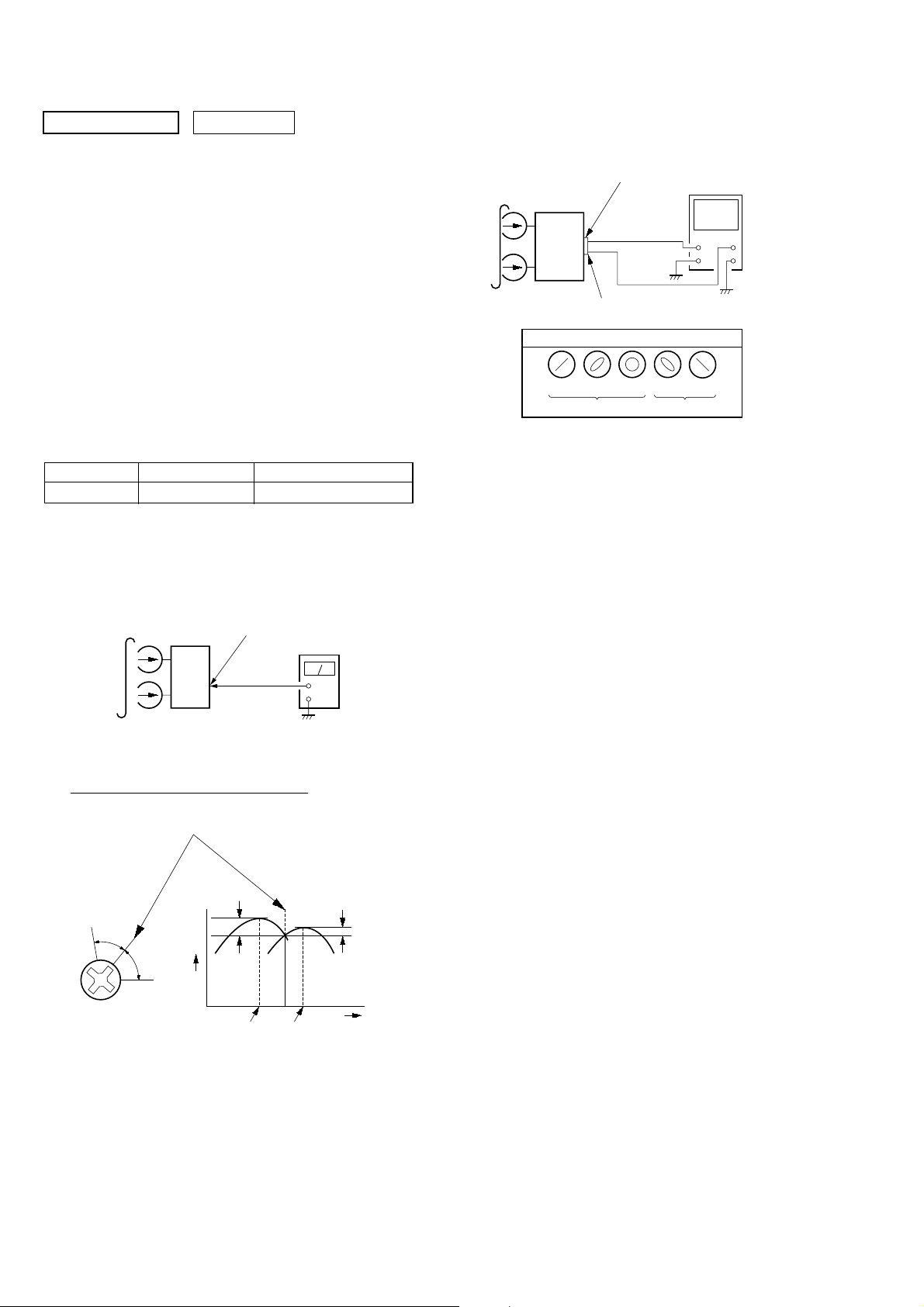
ELECTRICAL ADJUSTMENTS
DECK SECTION
Note: Confirm each contents of this section first of all. If the results are
not satisfied, do the adjustment.
0 dB=0.775 V
1. Demagnetize the record/playback head with a head
demagnetizer.
2. Do not use a magnetized screwdriver for the adjustments.
3. After the adjustments, apply suitable locking compound to the
parts adjust.
4. The adjustments should be performed with the rated power
supply voltage unless otherwise noted.
5. The adjustments should be performed in the order given in this
service manual. (As a general rule, playback circuit adjustment
should be completed before performing recording circuit
adjustment.)
6. The adjustments should be performed for both L-CH and RCH.
7. Switches and controls should be set as follows unless otherwise
specified.
•Test Tape
Tape Signal Used for
P-4-A63J 10 kHz, –10 dB Azimuth Adjustment
Record/Playback Head Azimuth Adjustment
Procedure:
1. Mode: Playback
3. Mode: Playback
MAIN board
test tape
P-4-A63J
(10 kHz, –10 dB)
L-CH
set
R-CH
in phase 45°90°135°180
SPEAKER terminals (SJ301
L-CH
R-CH
waveform of oscilloscope
good
oscilloscope
wrong
H
V
°
4. Repeat step 1 to 3 in playback (REV) mode.
5. After the adjustments, apply suitable locking compound to the
pats adjusted.
test tape
P-4-A63J
(10 kHz, –10 dB)
MAIN board
SPEAKER terminals (SJ301
L-CH, R-CH
level meter
set
+
–
2. T urn the adjustment screw and check output peaks. If the peaks
do not match for L-CH and R-CH, turn the adjustment screw
so that outputs match within 1dB of peak.
Output
level
within
1 dB
L-CH
peak
R-CH
peak
within
1 dB
Screw
position
L-CH
peak
Screw
position
R-CH
peak
18
 Loading...