

Page 1
HCD-CP100/CP100K
SERVICE MANUAL
Ver 1.2 2003.07
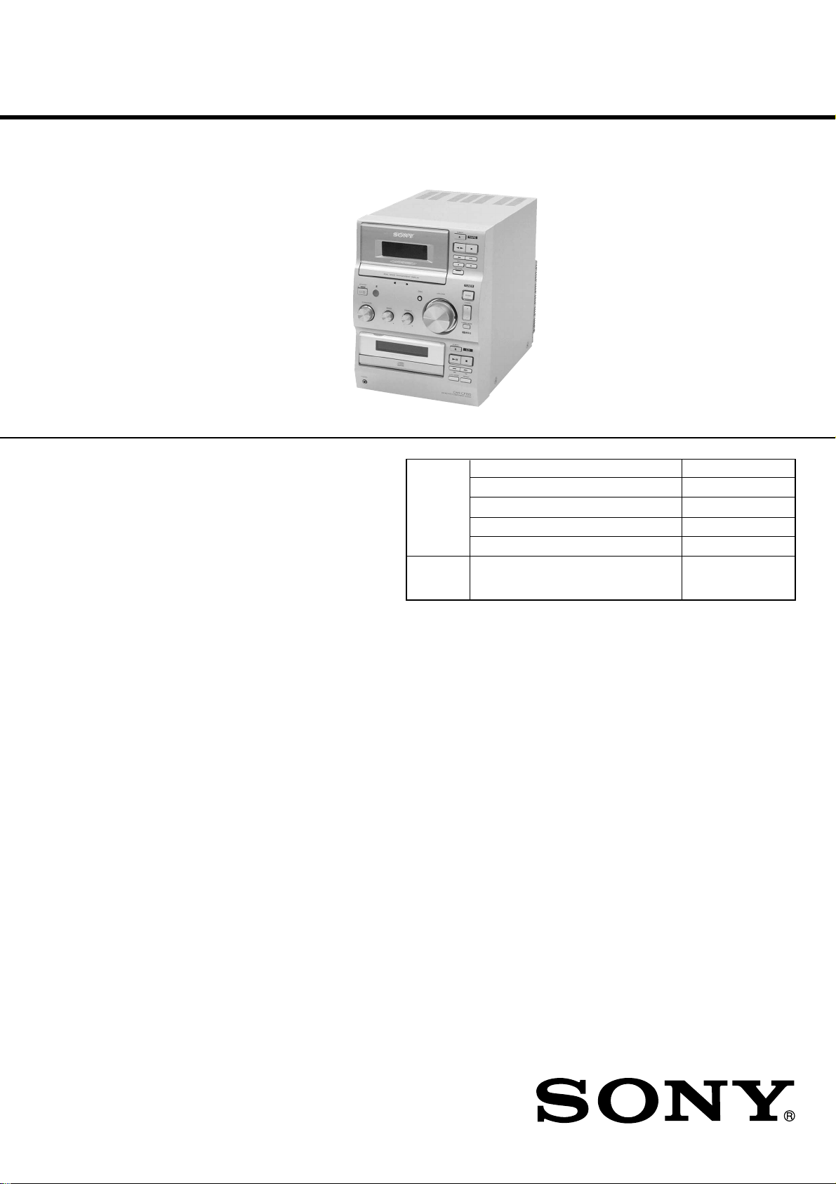
HCD-CP100/CP100K is the Amplifier, CD
player, Tape Deck and Tuner section in
CMT-CP100/CP100K.
CD
Section
Tape deck
Section
US Model
Canadian Model
AEP Model
UK Model
Australian Model
HCD-CP100
E Model
HCD-CP100/CP100K
Model Name Using Similar Mechanism NEW
CD Mechanism Type CDM55F-K6BD41A
Base Unit Name BU-K6BD41A
Optical Pick-up Block Name KSM-213DCP
Optical Pick-up Name KSS-213D
Model Name Using Similar Mechanism NEW
SPECIFICATIONS
Amplifier section
For the U.S. model
AUDIO POWER SPECIFICATIONS
POWER OUTPUT AND TOTAL
HARMONIC DISTORTION:
With 6-ohm loads, both channels driven, from
70 - 20,000 Hz; rated 18 watts per channel
minimum RMS power, with no more than 0.9%
total harmonic distortion from 250 milliwatts to
rated output.
North American model:
Continuous RMS power output (reference):
Total harmonic distortion less than 0.07% (6 ohms at
1 kHz, 18 W)
European model:
DIN power output (rated): 30 + 30 W
Continuous RMS power output (reference):
Music power output (reference):
35 + 35 W
(6 ohms at 1 kHz, 10%
THD)
(6 ohms at 1 kHz, DIN)
35 + 35 W
(6 ohms at 1 kHz, 10%
THD)
85 + 85 W
Other models:
The following measured at 230 V AC, 60 Hz
DIN power output (rated): 27 + 27 W
Continuous RMS power output (reference):
The following measured at 220 V AC, 60 Hz
DIN power output (rated): 23 + 23 W
Continuous RMS power output (reference):
Inputs
AUDIO IN MD (VIDEO) (phono jacks):
Outputs
OPTICAL DIGITAL OUT (CD):
PHONES (stereo phone jack):
SPEAKER: Active speaker system,
(6 ohms at 1 kHz, DIN)
32 + 32 W
(6 ohms at 1 kHz, 10%
THD)
(6 ohms at 1 kHz, DIN)
26 + 26 W
(6 ohms at 1 kHz, 10%
THD)
Sensitivity 500/250 mV,
impedance 47 kilohms
Optical
Accepts headphones with
an impedance of 8 ohms
or more
6 ohms
– Continued on next page –
9-873-803-13 Sony Corporation
2003G05-1 Home Audio Company
C 2003.07 Published by Sony Engineering Corporation
MICRO Hi-Fi COMPONENT SYSTEM
Page 2

HCD-CP100/CP100K
CD player section
System Compact disc and digital
Laser Semiconductor laser
Wavelength 780 - 790 nm
Frequency response 2 Hz - 20 kHz (±0.5 dB)
Tape player section
Recording system 4-track 2-channel stereo
Frequency response 50 - 13,000 Hz (±3 dB),
Wow and flutter ±0.15% W. Peak (IEC)
Tuner section
FM stereo, FM/AM superheterodyne tuner
FM tuner section
Tuning range
North American model: 87.5 - 108.0 MHz
Other models: 87.5 - 108.0 MHz
Antenna FM wire antenna
Antenna terminals 75 ohm unbalanced
Intermediate frequency 10.7 MHz
AM tuner section
Tuning range
Pan-American model: 530 - 1,710 kHz
European model: 531 - 1,602 kHz
Middle Eastern and Philippine models:
Other models: 530 - 1,710 kHz
Antenna AM loop antenna, external
Intermediate frequency 450 kHz
General
Power requirements
North American model: 120 V AC, 60 Hz
European model: 230 V AC, 50/60 Hz
Australian model: 220 - 240 V AC, 50/60 Hz
Mexican model: 120 V AC, 60 Hz
Other models: 110 - 120 V or 220 -
Power consumption
European model: See the nameplate
Other models: See the nameplate
Dimensions (w/h/d) Approx. 190 × 252 ×
Mass Approx. 5.6 kg
Design and specifications are subject to change
without notice.
audio system
(λ = 780 nm)
Emission
duration: continuous
using a Sony TYPE I
cassette
0.1% W. RMS (NAB)
±0.2% W. Peak (DIN)
(100-kHz step)
(50-kHz step)
(with the tuning interval
set at 10 kHz)
531 - 1,710 kHz
(with the tuning interval
set at 9 kHz)
(with the tuning interval
set at 9 kHz)
531 - 1,602 kHz
(with the tuning interval
set at 9 kHz)
(with the tuning interval
set at 10 kHz)
531 - 1,602 kHz
(with the tuning interval
set at 9 kHz)
antenna terminal
240 V AC , 50/60 Hz
Adjustable with voltage
selector
0.5 W (in the standby
mode)
345 mm incl. projecting
parts and controls
TABLE OF CONTENTS
1. SERVICING NOTES ............................................... 4
2. GENERAL
Location of Controls ....................................................... 5
Setting the Time .............................................................. 6
3. DISASSEMBLY
3-1. Disassembly Flow ........................................................... 7
3-2. Cover (Upper) ................................................................. 8
3-3. CD Lid............................................................................. 8
3-4. Front Panel Section ......................................................... 9
3-5. Tape Mechanism Deck.................................................... 9
3-6. CD Mechanism Deck (CDM55F-K6BD41A)................ 10
3-7. Base Unit (BU-K6BD41A)............................................. 10
3-8. Loading Board ................................................................. 11
3-9. Cam (CDM55) ................................................................ 11
4. TEST MODE.............................................................. 12
5. ELECTRICAL ADJUSTMENTS
Deck Section ................................................................... 13
CD Section ...................................................................... 13
6. DIAGRAMS
6-1. Block Diagram – CD SERVO Section – ........................ 14
6-2. Block Diagram – MAIN Section –................................. 15
6-3. Block Diagram
– DISPLAY/POWER SUPPLY Section – ...................... 16
6-4. Note for Printed Wiring Boards and
Schematic Diagrams ....................................................... 17
6-5. Printed Wiring Board – CD Board – .............................. 18
6-6. Schematic Diagram – CD Board – ................................. 19
6-7. Printed Wiring Board – TC Board –............................... 20
6-8. Schematic Diagram – TC Board –.................................. 21
6-9. Schematic Diagram
– MAIN (1/2)/LOADING Board –................................. 22
6-10. Schematic Diagram – MAIN Board (2/2) – ................... 23
6-11. Printed Wiring Board – MAIN Board – ......................... 24
6-12. Printed Wiring Boards
– SWITCH/TC SWITCH/PRISM Boards –................... 26
6-13. Schematic Diagram
– SWITCH/TC SWITCH/PRISM Boards –................... 27
6-14. IC Pin Function Description ........................................... 28
6-15. Printed Wiring Boards
– LCD/HEADPHONE Boards – .................................... 29
6-16. Schematic Diagram – LCD/HEADPHONE Boards – ... 29
6-17. Printed Wiring Board – POWER Board – ...................... 30
6-18. Schematic Diagram – POWER Board –......................... 31
7. EXPLODED VIEWS
7-1. Cover Section.................................................................. 35
7-2. Front Panel Section ......................................................... 36
7-3. Chassis Section ............................................................... 37
7-4. CD Mechanism Deck (CDM55F-K6BD41A)................ 38
7-5. Base Unit (BU-K6BD41A)............................................. 39
8. ELECTRICAL PARTS LIST ............................... 40
2
Page 3
HCD-CP100/CP100K
1.5 k
Ω
0.15 µF
AC
voltmeter
(0.75 V)
To Exposed Metal
Parts on Set
Earth Ground
Notes on chip component replacement
• Never reuse a disconnected chip component.
• Notice that the minus side of a tantalum capacitor may be damaged by heat.
Flexible Circuit Board Repairing
• Keep the temperature of the soldering iron around 270 ˚C during repairing.
• Do not touch the soldering iron on the same conductor of the
circuit board (within 3 times).
• Be careful not to apply force on the conductor when soldering
or unsoldering.
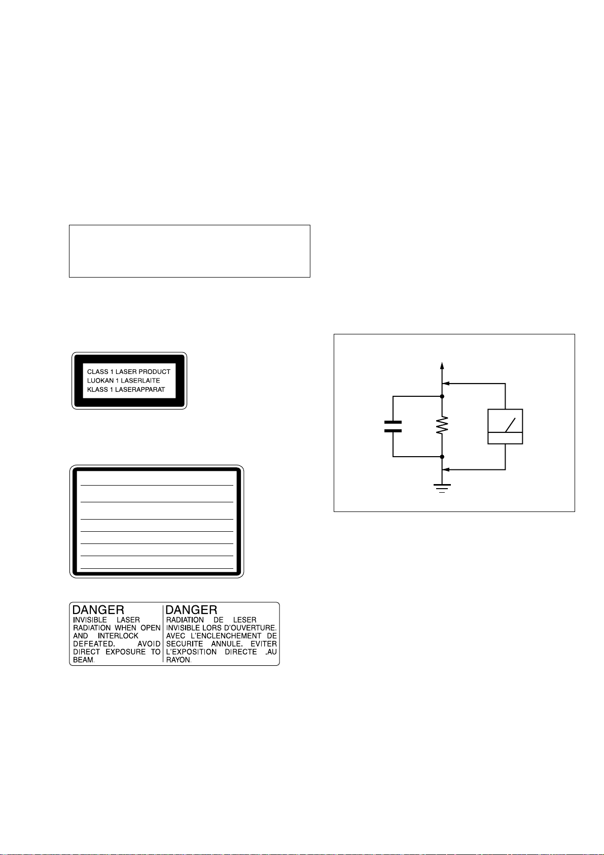
CAUTION
Use of controls or adjustments or performance of procedures
other than those specified herein may result in hazardous radiation exposure.
This appliance is classified as a CLASS 1 LASER product.
The CLASS 1 LASER PRODUCT MARKING is located on
the rear exterior.
SAFETY CHECK-OUT
After correcting the original service problem, perform the following safety check before releasing the set to the customer:
Check the antenna terminals, metal trim, “metallized” knobs,
screws, and all other exposed metal parts for AC leakage.
Check leakage as described below.
LEAKAGE TEST
The AC leakage from any exposed metal part to earth ground and
from all exposed metal parts to any exposed metal part having a
return to chassis, must not exceed 0.5 mA (500 microamperes.).
Leakage current can be measured by any one of three methods.
1. A commercial leakage tester , such as the Simpson 229 or RCA
WT -540A. Follow the man ufacturers’ instructions to use these
instruments.
2. A battery-operated AC milliammeter . The Data Precision 245
digital multimeter is suitable for this job.
3. Measuring the voltage drop across a resistor by means of a VOM
or battery-operated A C voltmeter . The “limit” indication is 0.75
V, so analog meters must have an accurate low-voltage scale.
The Simpson 250 and Sanwa SH-63Trd are examples of a passive VOM that is suitable. Nearly all battery operated digital
multimeters that have a 2 V A C range are suitable. (See Fig. A)
Laser component in this product is capable of emitting radiation
exceeding the limit for Class 1.
The following caution label is located inside the unit.
CAUTION :
INTERLOCKS DEFEATED. AVOID EXPOSURE TO BEAM.
ADVARSEL :
SIKKERHEDSAFBRYDERE ER UDE AF FUNKTION. UNDGÅ UDSAETTELSE
FOR STRÅLING.
VORSICHT :
ABDECKUNG GEÖFFNET UND SICHEREITSVERRIEGELUNG
ÜBERBRÜCKT. NICHT DEM STRAHL AUSSETZEN.
VARO! :
TIINA NÄKYMÄTTÖMÄLLE LASERSÄTEILYLLE. ÄLÄ KATSO SÄTEESEEN.
VARNING :
OCH SPÄRREN ÄR URKOPPLAD. BETRAKTA EJ STRÅLEN.
ADVERSEL :
SIKKERHEDSLÅS BRYTES. UNNGÅ EKSPONERING FOR STRÅLEN.
VIGYAZAT! :
GÁRVESZÉLY! KERÜLJE A BESUGÁRZÁST!
COMPONENTS IDENTIFIED BY MARK 0 OR DOTTED
LINE WITH MARK 0 ON THE SCHEMATIC DIA GRAMS
AND IN THE PARTS LIST ARE CRITICAL TO SAFE
OPERATION. REPLACE THESE COMPONENTS WITH
SONY PARTS WHOSE PART NUMBERS APPEAR AS
SHOWN IN THIS MANU AL OR IN SUPPLEMENTS PUBLISHED BY SONY.
INVISIBLE LASER RADIATION WHEN OPEN AND
USYNLIG LASERSTRÅLING VED ÅBNING NÅR
UNSICHTBARE LASERSTRAHLUNG, WENN
AVATTAESSA JA SUOJALUKITUS OHITETTAESSA OLET ALT-
OSYNLING LASERSTRÅLING NÄR DENNA DEL ÄR ÖPPNAD
USYNLIG LASERSTRÅLING NÅR DEKSEL ÅPNES OG
A BURKOLAT NYITÁSAKOR LÁTHATATLAN LÉZERSU-
SAFETY-RELATED COMPONENT WARNING!!
Fig. A. Using an AC voltmeter to check AC leakage.
ATTENTION AU COMPOSANT AYANT RAPPORT
À LA SÉCURITÉ!
LES COMPOSANTS IDENTIFIÉS P AR UNE MARQUE 0
SUR LES DIAGRAMMES SCHÉMA TIQ UES ET LA LISTE
DES PIÈCES SONT CRITIQUES POUR LA SÉCURITÉ
DE FONCTIONNEMENT. NE REMPLACER CES COMPOSANTS QUE PAR DES PIÈCES SONY DONT LES
NUMÉROS SONT DONNÉS DANS CE MANUEL OU
DANS LES SUPPLÉMENTS PUBLIÉS PAR SONY.
3
Page 4
HCD-CP100/CP100K
R
SECTION 1
SERVICING NOTES
NOTES ON HANDLING THE OPTICAL PICK-UP
BLOCK OR BASE UNIT
The laser diode in the optical pick-up block may suffer electrostatic break-down because of the potential difference generated
by the charged electrostatic load, etc. on clothing and the human
body.
During repair, pay attention to electrostatic break-down and also
use the procedure in the printed matter which is included in the
repair parts.
The flexible board is easily damaged and should be handled with
care.
NOTES ON LASER DIODE EMISSION CHECK
The laser beam on this model is concentrated so as to be focused
on the disc reflective surface by the objective lens in the optical
pick-up block. Therefore, when checking the laser diode emission, observe from more than 30 cm away from the objectiv e lens.
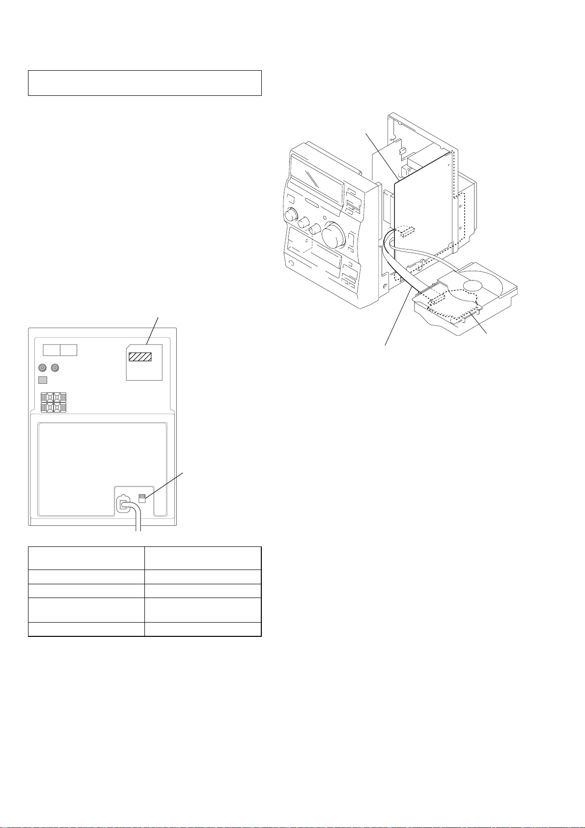
• MODEL IDENTIFICATION
– Rear Panel –
Power Voltage Indication
SERVICE POSTION
In checking the CD block, prepare jig (extension cable J-2501011-B).
MAIN board
CD board
Connect jig (extension cable J-2501-011-B)
to the MAIN board (CN101) and CD board (CN101).
Model
US, CND, MX models
AEP, UK models
E, EA, AR, SP, AUS models
KR model
• Abbreviation
AR : Argentina model.
AUS : Australian model.
CND : Canadian model.
EA : Saudi Arabia model.
KR : Korean model.
MX : Mexican model.
SP : Singapore model.
TH : Thailand model.
VOLTAGE SELECTO
Switch
Pow er Voltage
Incdication
AC: 120 V 60 Hz 75 W
AC: 230 V -50/60 Hz 75 W
AC: 110 – 120/
220 – 240 V / 50/60 Hz 75 W
220 V/60 MHz 75 W
4
Page 5
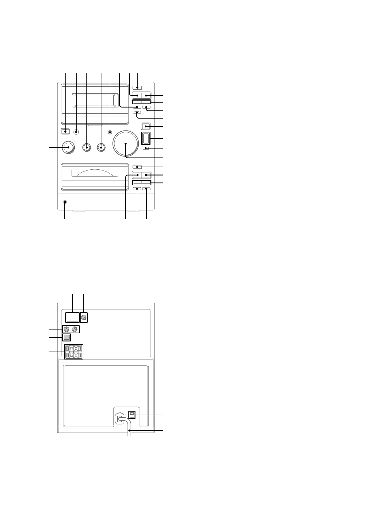
• LOCATION OF CONTROLS – Front View –
1 2 5 8
?/1
A
63 4 7
wf
Z
Y
m
zX
Z
ux
.>
mM
w;
wawd ws
HCD-CP100/CP100K
SECTION 2
GENERAL
1 STANDBY I/1 button and indicator
2 Remote sensor
3 BASS knob
x
9
M
q;
qa
qs
qd
qf
qg
qh
qj
qk
ql
4 TREBLE knob
5 DSG button and indicator
6 TAPE REC z button
7 TAPE Y button
8 TAPE EJECT Z button
9 TAPE x button
0 TAPE m / M button
qa TAPE X button
qs CD SYNC button and indicator
qd TUNER BAND button
qf TUNING +/– button
qg TUNING MODE button
qh VOLUME knob
qj CD EJECT Z button
qk CD x button
ql CD . m / M > button
w; REPEAT button
wa PLAY MODE button
ws CD u button
wd PHONES jack
wf FUNCTION knob
– Rear View –
1
3
4
5
2
1 AM ANTENNA terminals
2 FM ANTENNA jack or terminals
3 AUDIO IN MD (VIDEO) jacks
4 CD DIGITAL OUT OPTICAL connector
5 SPEAKER terminals
6 VOLTAGE SELECTOR switch
7 AC power cord
6
7
5
Page 6
HCD-CP100/CP100K
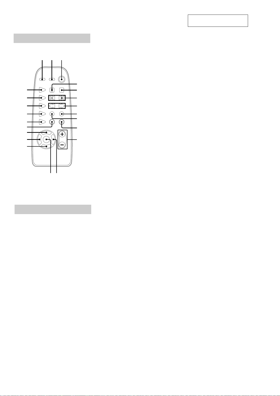
Remote Control
This section is extracted from
instruction manual.
ws
wa
w;
ql
qk
qj
qh
qg
qf
123
qsqd
4
5
6
7
8
9
0
qa
1 DSG button
2 DISPLAY button
3 I/1 (power) button
4 X button
5 x button
6 . / > buttons
7 m / M buttons
8 z REC button
9 PLAY MODE button
0 TUNING MODE button
qa VOLUME +/– buttons
qs TIMER SELECT button
qd ENTER button
qf SLEEP button
qg TIMER SET button
qh MEMORY button
qj STEREO/MONO button
qk CD REPEAT button
ql DIR MODE button
w; TAPE Y button
wa TUNER/BAND button
ws CD N button
Setting the time
1
Turn on the system.
2
Press TIMER SET on the remote.
If you are setting the clock for the first time,
go to step 5.
3
Press ./> on the remote
repeatedly until “SET CLOCK” appears
in the display.
4
Press ENTER on the remote.
The hour indication flashes.
5
Press ./> on the remote
repeatedly to set the hour.
6
Press ENTER on the remote.
The minute indication flashes.
7
Press ./> on the remote
repeatedly to set the minute.
8
Press ENTER on the remote.
The clock will begin operating.
To reset the system clock
Start over from step 1.
6
Page 7
• This set can be disassembled in the order shown below.
3-1. DISASSEMBLY FLOW
Set
3-2. COVER (UPPER)
(Page 8)
3-3. CD LID
(Page 8)
HCD-CP100/CP100K
SECTION 3
DISASSEMBLY
3-4. FRONT PANEL SECTION
(Page 9)
3-5. TAPE MECHANISM DECK
(Page 9)
3-6. CD MECHANISM DECK
(CDM55F-K6BD41A)
(Page 10)
3-7. BASE UNIT
(BU-K6BD41A)
(Page 10)
3-8. LOADING BOARD
(Page 11)
3-9. CAM (CDM55)
(Page 11)
7
Page 8
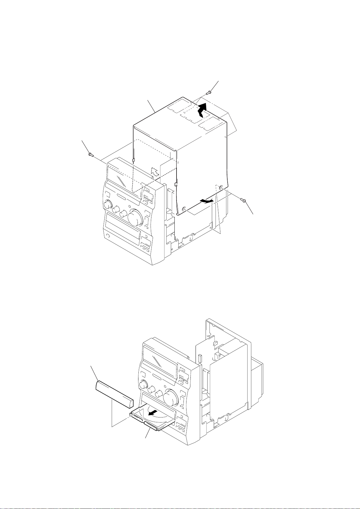
HCD-CP100/CP100K
s
Note: Follow the disassembly procedure in the numerical order given.
3-2. COVER (UPPER)
3
cover (upper)
2
two case screws
1
four screws
(BVTP4
×
8)
3-3. CD LID
2
CD lid
2
two case screw
1
tray
Note: Open the tray by supplying the power.
8
Page 9
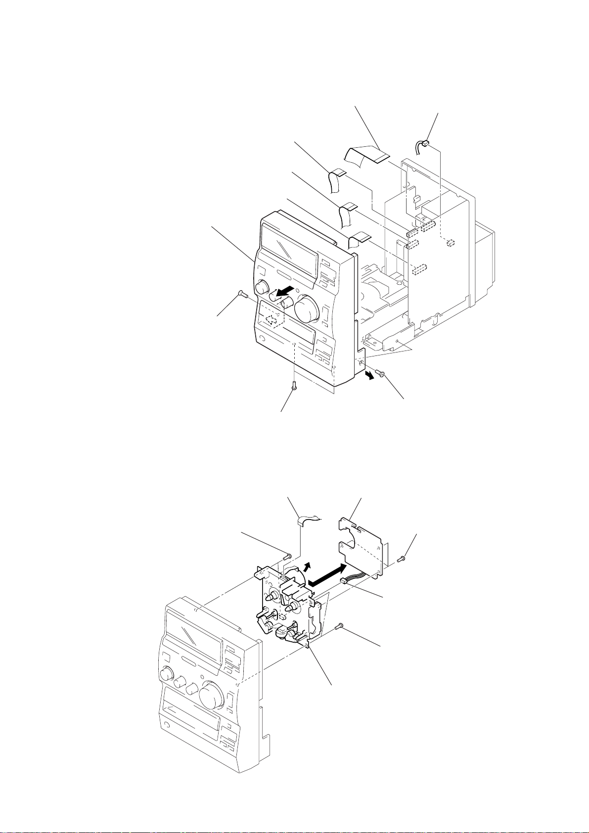
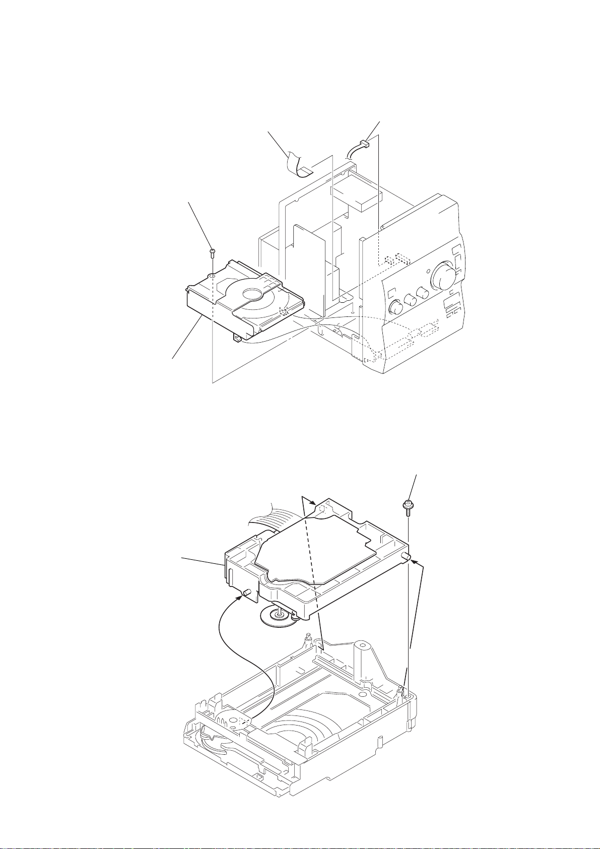
3-4. FRONT PANEL SECTION
)
1
5
front panel section
1
wire (flat type) 18p
(CN802)
1
wire (flat type) 20p
(CN804)
wire (flat type) 21p
(CN301)
1
wire (flat type) 23p
(CN801)
HCD-CP100/CP100K
2
connector
(CN501)
4
screw (KTP3 × 6)
3-5. TAPE MECHANISM DECK
6
two screws
(BTP3
3
two screws
(BTP3
5
wire flat type 9P
(CN302)
×
8)
4
screw (KTP3 × 6)
×
8)
4
TC board
1
three screws
(BVTT2.6
2
3
connector
(CNP1)
×
5
7
tape machanism deck
6
two screws
(BTP3
×
8)
9
Page 10
HCD-CP100/CP100K
3-6. CD MECHANISM DECK (CDM55F-K6BD41A)
1
flexible flat cable (19core)
(CN101)
3
tscrew
(BTP3
×
8)
2
connector
(CN401)
4
CD mechanism deck (CDM55F-K6BD41A)
3-7. BASE UNIT (BU-K6BD41A)
2
base unit (BU-K6BD41A)
1
floating screw
(PTPWHM2.6)
10
Page 11
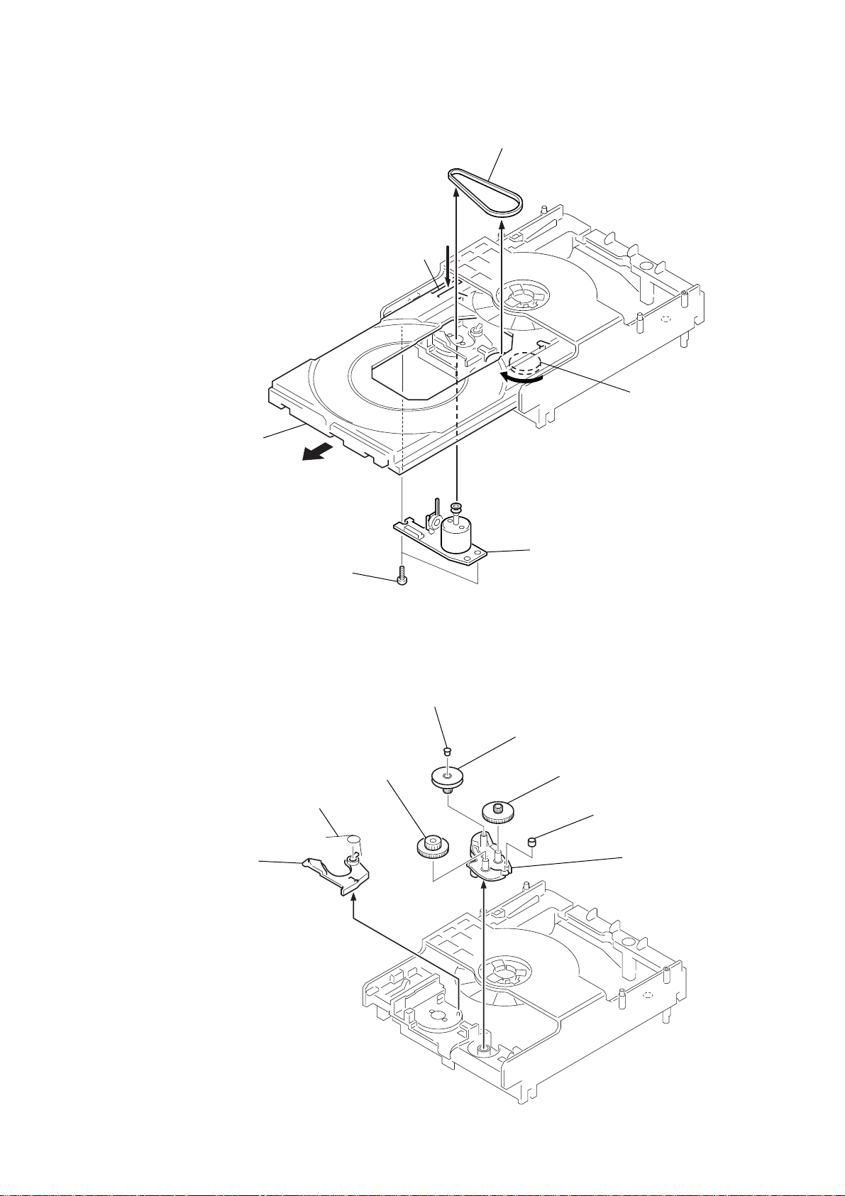
3-8. LOADING BOARD
2
belt (CDM55)
B
3
Pull the tray pushing B.
4
two screws
(BTP2.6
×
6)
5
LOADING board
1
Rotate the gear(B) in
the direction of arrow
A
.
A
HCD-CP100/CP100K
3-9. CAM (CDM55)
2 lever (SW)
1 torsion spring
6 gear (B)
3 spacer (55)
4 pulley (LDG)
5 gear (A)
7 roller
8 cam (CDM55)
11
Page 12
HCD-CP100/CP100K
SECTION 4
TEST MODE
[Cold Reset]
• The cold reset clears all data including preset data stored in the
RAM to initial conditions. Execute this mode when returning
the set to the customer.
Procedure:
1. Turn ON the power.
2. Press three buttons x (TAPE), x (CD), and [BAND]
simultaneously.
3. The set is reset.
[Liquid Crystal Display All Lit Check Mode]
Procedure:
1. Set to standby state.
2. Press three buttons of x (TAPE), x (CD), and
[TUNING MODE] simultaneously.
3. Liquid crystal display are all turned on.
4. T o e xit from this mode, press the I/1 button to turn the power
OFF.
[Tape Deck Aging Mode]
This mode can be used for operation check of tape deck section.
Procedure:
1. Set a tape in the tape deck.
2. Set to standby state.
3. Press three buttons of x (TAPE), x (CD), and [TUNING +]
simultaneously.
4. The aging is executed in bellow sequence.
5. To exit from the aging mode, press the I/1 button to turn the
power OFF.
[CD Aging Mode]
This mode can be used for operation check of CD section.
Procedure:
1. Load a CD disc.
2. Set to standby state.
3. Press three buttons of x (TAPE), x (CD), and [TUNING --]
simultaneously.
4. The aging is executed in bellow sequence.
5. To exit from the aging mode, press the I/1 button to turn the
power OFF.
Aging mode sequence:
Start
Open the disc tray
Close the disc tray
Play the last track
Aging mode sequence:
Start
FWD Play
REC pause for 3 seconds
FWD REC
Fast forward
REV Play
REC pause for 3 seconds
Shut off
1 minute
Shut off
3 minutes
Shut off
1 minute
12
REV REC
3 minutes
Rewind
Shut off
Page 13
SECTION 5
)
V
ELECTRICAL ADJUSTMENTS
HCD-CP100/CP100K
DECK SECTION
Note: Confirm each contents of this section first of all. If the results are
not satisfied, do the adjustment.
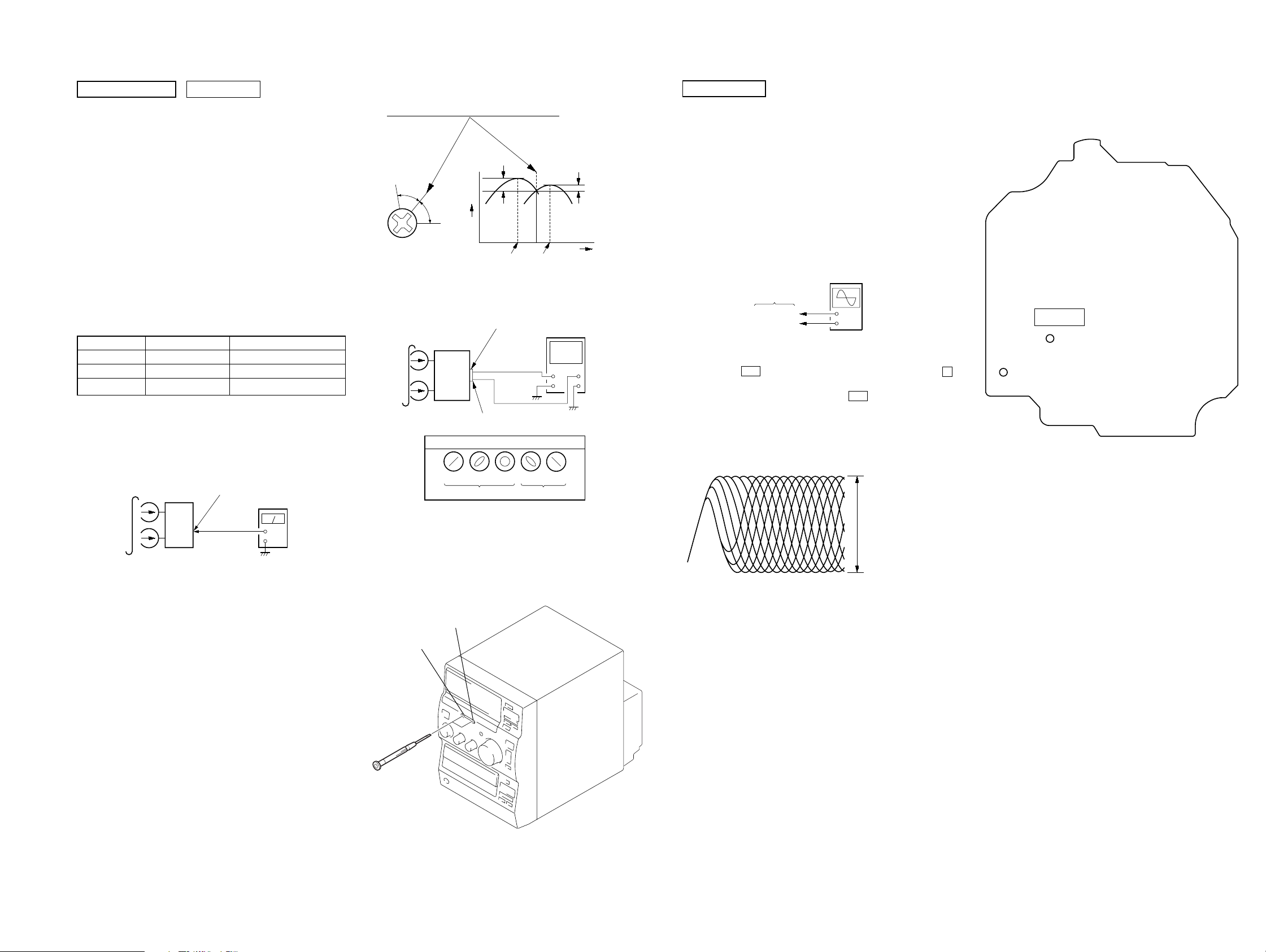
0 dB=0.775 V
1. Demagnetize the record/playback head with a head
demagnetizer.
2. Do not use a magnetized screwdriver for the adjustments.
3. After the adjustments, apply suitable locking compound to the
parts adjust.
4. The adjustments should be performed with the rated power
supply voltage unless otherwise noted.
5. The adjustments should be performed in the order given in this
service manual. (As a general rule, playback circuit adjustment
should be completed before performing recording circuit
adjustment.)
6. The adjustments should be performed for both L-CH and RCH.
7. Switches and controls should be set as follows unless otherwise
specified.
• Test Tape
Tape Signal Used for
P-4-A100 10 kHz, –10 dB Azimuth Adjustment
WS-48B 3 kHz, 0 dB Tape Speed Adjustment
P-4-L300 315 Hz, 0 dB Level Adjustment
Record/Playback Head Azimuth Adjustment
Procedure:
1. Mode: Playback
test tape
P-4-A100
(10 kHz, –10 dB)
MAIN board
SPEAKER terminals (SJ301
L-CH, R-CH
level meter
set
+
–
2. T urn the adjustment screw and check output peaks. If the peaks
do not match for L-CH and R-CH, turn the adjustment screw
so that outputs match within 1dB of peak.
Output
level
within
1 dB
L-CH
peak
R-CH
peak
within
1 dB
Screw
position
L-CH
peak
Screw
position
R-CH
peak
3. Mode: Playback
MAIN board
test tape
P-4-A100
(10 kHz, –10 dB)
L-CH
MAIN
board
CN301
set
R-CH
in phase 45°90°135°180
SPEAKER terminals (SJ301)
L-CH
R-CH
waveform of oscilloscope
good
oscilloscope
wrong
H
V
°
4. Repeat step 1 to 3 in playback (REV) mode.
5. After the adjustments, apply suitable locking compound to the
pats adjusted.
CD SECTION
Note:
1. CD Block is basically constructed to operate without
adjustment.
2. Use YEDS-18 disc (3-702-101-01) unless otherwise indica ted.
3. Use an oscilloscope with more than 10 MΩ impedance.
4. Clean the object lens by an applicator with neutral detergent
when the signal level is low than specified value with the
following checks.
5. Check the focus bias check when optical block is replaced.
Focus Bias Check
oscilloscope
(DC range)
BD board
TP (RF)
TP (VC)
Procedure :
1. Connect oscilloscope to TP (RF) and TP (VC) on the CD board.
2. Press the I/1 button to turn the power on, and press the Z
(CD) button to open the CD disc tray.
3. Put disc (YEDS-18) in and press the u (CD) button to playback.
4. Confirm that oscilloscope waveform is as shown in the figure
below. (eye pattern)
A good eye pattern means that the diamond shape ( ) in the
center of the waveform can be clearly distinguished.
+
–
s
VOLT/DIV: 200 m
TIME/DIV: 500 ns
level:
1.2 ± 0.1 Vp-p
Checking Location:
– CD BOARD (Conductor Side) –
IC103
TP (RF)
TP (VC)
Adjustment Location:
reverse
forward
1313
Page 14
HCD-CP100/CP100K
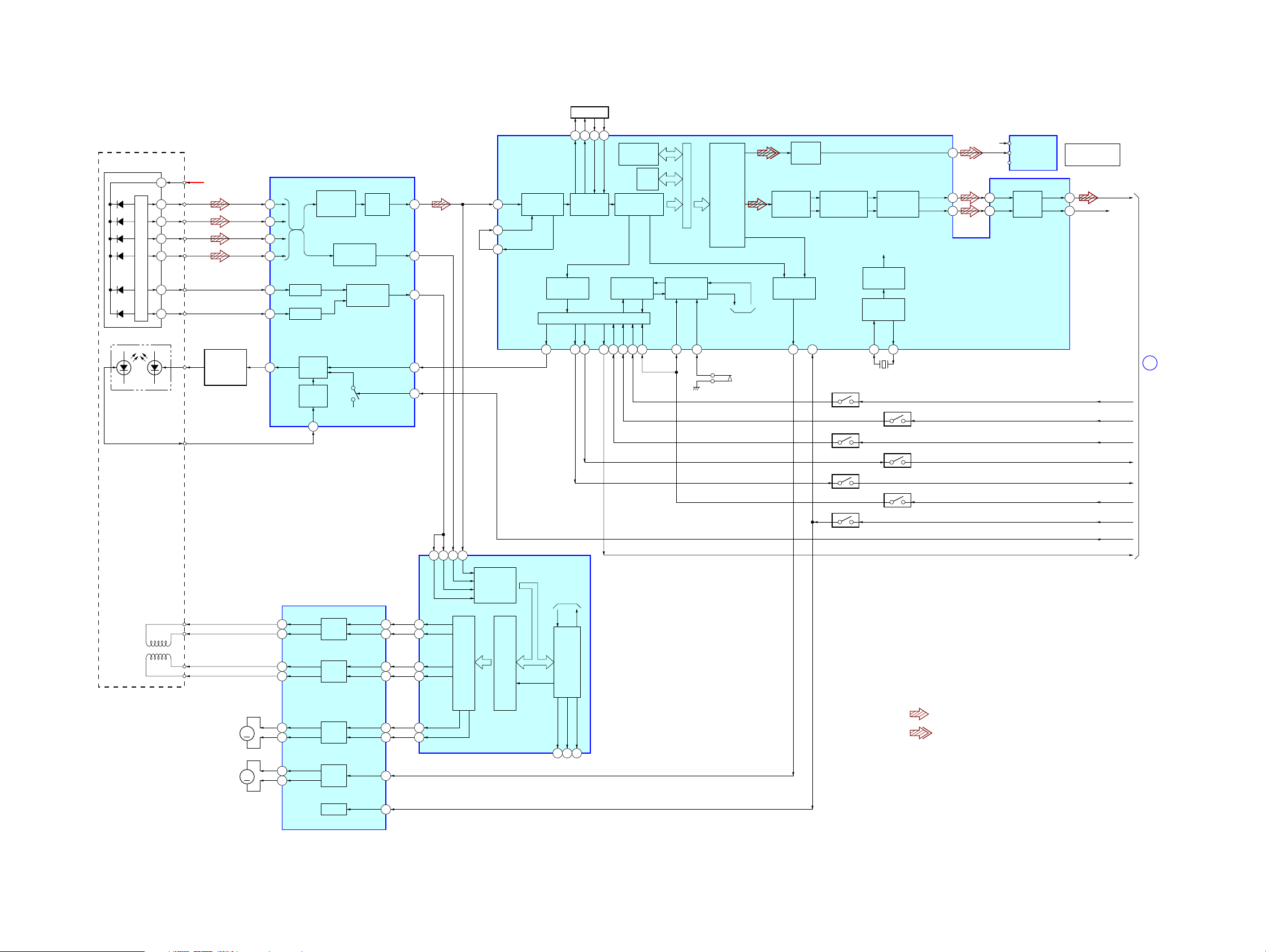
6-1. BLOCK DIAGRAM – CD SERVO Section –
SECTION 6
DIAGRAMS
PICK-UP BLOCK
(KSS-213DCP)
DETECTOR
LASER DIODE
(TRACKING)
(FOCUS)
OPTICAL
7 D+5V
4
2
1
5
I-V AMP
10
6
LDPD
2-AXIS DEVICE
VCC
LD
PD
AUTOMATIC
POWER
CONTROL
Q101
M102
(SLED)
M101
(SPINDLE)
FILTER
54 56 53 55
ERROR
RF AMP
FOCUS/TRACKING ERROR AMP
A
5
B
6
C
7
D
8
F
10
FI-V AMP
E
11
EI-V AMP
LD
3
FOCUS/TRACKING COIL DRIVE,
SPINDLE/SLED MOTOR DRIVE
CH2OUTF
12
CH2OUTR
11
CH1OUTF
14
CH1OUTR
13
CH3OUTF
17
MM
MM
18
15
16
CH3OUTR
CH4OUTF
CH4OUTR
APC LD
AMP
APC PD
AMP
PD
4
IC103
RF
SUMMING
AMP
ERROR AMP
IC102
MOTOR
COIL
DRIVE
DRIVE
COIL
DRIVE
MOTOR
DRIVE
MOTOR
DRIVE
FOCUS
TRACKING
ERROR AMP
CH2 FIN
CH2RIN
CH1FIN
CH1RIN
CH3FIN
CH3RIN
CH4SIN
RF EQ
AMP
RFO
LD ON
HOLD SW
5
6
2
3
24
23
25
RFAC
16
FE
14
TE
13
22
21
41 39 4340
FE
TE
SE
RFDC
A/D
CONVERTER
TRDR
31
TFDR
30
FRDR
33
FFDR
32
SFDR
28
SRDR
29
PWM GENERATOR
FOCUS/TRACKING/SLED
ASYMMETRY
51
CORRECTION
ASYI
49
ASYO
48
SERVO DSP
FOCUS/TRACKING/SLED
SUBCODE
PROCESSOR
XLON
SERVO
INTERFACE
IC101 (1/2)
FOK
TO
MIRR/DFCT/FOK
DFCT
23 2224
FILI
PCO
FILO
CLTV
DIGITAL
PLL
CPU INTERFACE
SCOR
SENS
SQSO
DIGITAL SERVO
PROCESSOR
IC101 (2/2)
DETECTOR
MIRR
CORRECTOR
EFM
DEMODULATOR
SERVO AUTO
SEQUENCER
DATA
CLOK
XLAT
16k
RAM
SQCK
2576208114
DIGITAL SIGNAL PROCESSOR,
DIGITAL FILTER, D/A CONVERTER
IC101 (1/2)
D/A
INTERFACE
INTERNAL BUS
SERVO
INTERFACE
MIRR/DFCT/FOK DETECTOR
SSTP
IC101 (2/2)
SCLK
9 27
TO
S101
(LIMIT)
DIGITAL
SERIAL
IN
INTERFACE
DIGITAL
CLV
MDP
26
OUT
NOISE SHAPER
XRST
3
DIGITAL
FILTER
Q803
Q804
Q806
Q802
CD ON SWITCH
CLOCK
GENERATOR
TIMING
LOGIC
XTAL
16.9344MHz
Q802 – 808
VDD
515171
76
AIN1
AIN2
PWM
&
INTEGRATOR
XTAO
6766
X101
Q805
Q807
Q808
D OUT
AOUT1
AOUT2
60
70
77
• R-CH : R-ch is omitted due to same as L-ch.
• SIGNAL PATH
: CD PLAY (ANALOG)
: CD PLAY (DIGITAL OUT)
OPTICAL
TRANSCVER
IC321
BUFFER
LOUT1
LOUT2
OPTICAL
DIGITAL OUT (CD)
72
75
CD L IN
DATA
LATCH
SENS
SQSO
SQCK
XRST
HOLD
C SCOR
CLK
R-CH
A
(Page 15)
MUTE
MUTE
20
1414
Page 15
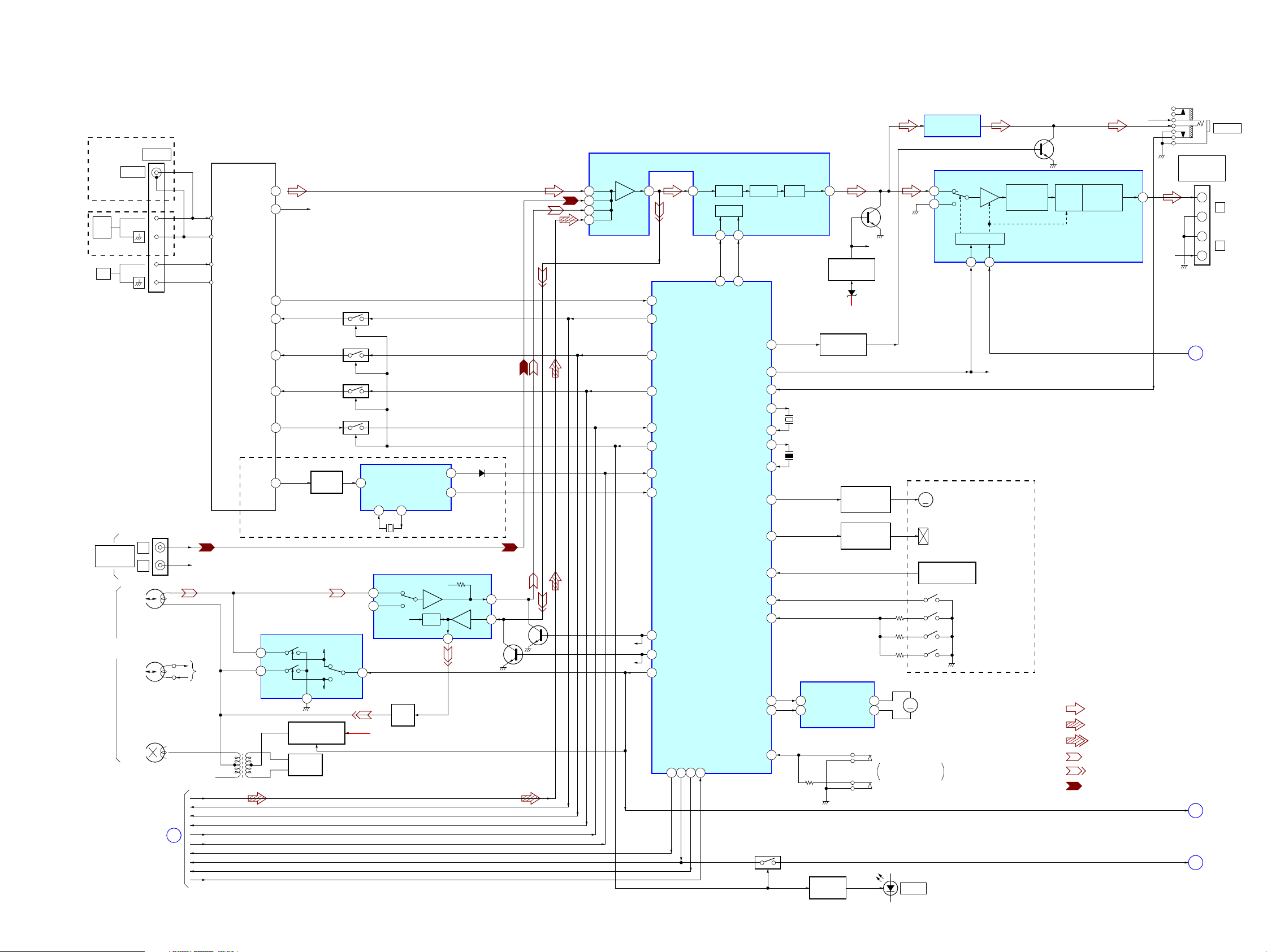
6-2. BLOCK DIAGRAM – MAIN Section –
HCD-CP100/CP100K
(EXCEPT CP100 : US, CND)
ANENNA
FM75Ω
(CP100 : US, CND)
FM
75Ω
AM
AUDIO IN
MD (VIDEO)
HRPE901
(RECORD/PLAYBACK/ERASE)
L
R
L-CH
R-CH
(ERASE)
(Page 14)
SJ302
SJ301
SPEAKER
+
–
–
+
B
D
C
J301
PHONES
L
R
(Page 16)
(Page 16)
(Page 16)
OUT
R-CH
IMPEADANCE
USE 6 – 16Ω
14
R-CH
REG CON
REC/PB
FM ON
INPUT SELECT SWITCH,
MIX, TONE CONTROL,
ELECTRICAL VOLUME
TU1
TUNER PACK
LINE
OUT2
1
L-CH
2
FM ANT
ANT GND
AM ANT
ANT GND
R-CH
R-CH
CD L IN
DATA
CLK
LATCH
A
SENS
SQSO
SQCK
XRST
HOLD
C SCOR
R-CH R-CH
Q809 – 811, 813
TUNER ON/OFF
4
TUNED
9
DI
8
CK
10
CE
7
DO
(CP100 : AEP, UK)
3
FM DET MIX
REC/PB SWITCHING
IC402
(REC)
1
(PB)
3
2
BIAS
OSC
T401
REC BIAS SWITCH
Q402, 403
BIAS OSC
Q401
Q810
Q809
Q811
Q813
DET AMP
Q812
R-CH
R-CH
SWITCH
4.332MHz
(SW)
4
X803
4
X1 X0
13 14
B IN L
23
A IN L
24
B+
(+8V)
RDATA
RCLK
RDS DECODER
REC/PB AMP, EQ AMP
IC401
R-CH
R-CH
ALC
REC OUT L
T403
BIAS
TRAP
IC804
16
D806
2
16
PB L
20
REC
IN L
14
MUTING
Q407
MUTING
Q414
C2
6
A2
2
D2
8
E2
10
31 30 17
LINE
AMP
17
19
18
25
12
96 L MUTE
R-CH
87 REC MUTE
R-CH
95
IC323
VOL2 OUT2
DATA CLK
(MPEG RST) TUNED
5
(TU DATA) C DATA/TU DATA
8
(TU CLK) C CLK/TU CLK
(TU CE) C LATCH/
TU CE
(TU COUNT) SENS2/
TU COUNT
TU ON
(S SI) C SQSO/
RDS DATA
2
(TUNED) RDS IN
SYSTEM CONTROLLER
IC801 (1/2)
REC/PB
(PBC LED) TRAY CLOSE
(S CLK) C SQCK
C XRST/FM ON
(S REQ) HOLD
11 86 14 100
C SCOR (S ACK)
TREBLE
14 15
SDA
88 28
(S SO) TRAY OPEN
TRAY SW (JOG H)
LOGIC
AU MUTE
AMP MUTE
(MIC CHECK)
H/P CHECK
MOT CON
SOL CON
TAPE END
MIDDLE BASS
SCK
(JOG G)
TEX
XTAL1
EXTAL1
T MODE
TC SW
TX
Q801
MUTING
Q200
R-CH
MUTING DRIVE
Q330
B+ (+8V)
X802
32.768KHz
X801
4.19MHz
6
INPUT2
5
INPUT1
LED DRIVE
MUTING DRIVE
Q312, 313
CAPSTAN/REEL
MOTOR DRIVE
PLUNGER DRIVE
LOADING
MOTOR DRIVE
IC320
Q854
Q601, 602
TRIGGER
Q603, 604
OUT2
OUT1
10
2
OPEN/CLOSE DETECT
97
22
24
92
93
40
39
4
10
1
6
32
13
15
33
HEADPHONE AMP
(TAPE DECK BLOCK)
MM
TAPE END DETECT
M901
MM
(LOADING)
SI
DISC TRAY
D856, 857
TUNER
IC324
IN+
3
4
IN–
STANDBY/MUTE
MUTE STBY
SENSOR
10 9
R-CH
MOS GAIN &
LEVEL SHIFT
ING STAGE
MUTING
Q815, 817
MOS
OUTPUT
STAGE
SHORT
CIRCUIT
PROTECTION
POWER AMP
IC201
• R-CH : R-ch is omitted due to same as L-ch.
• SIGNAL PATH
: TUNER
: CD PLAY (ANALOG OUT)
: CD PLAY (OPTICAL OUT)
: TAPE (PLAY)
: TAPE (RECORD)
: MD
1515
Page 16

HCD-CP100/CP100K
6-3. BLOCK DIAGRAM – DISPLAY/POWER SUPPLY Section –
(Page 15)
D859
CD SYNC
(Page 15)
(Page 15)
D858
DSG
VOLUME
FUNCTION
D
C
CB
RV801
RV802
TREBLE
RV803
BASS
RV804
REC/PB
LIQUID CRYSTAL
FM ON
REG CON
ROTARY
ENCODER
RV801
ROTARY
ENCODER
RV802
ROTARY
ENCODER
RV803
ROTARY
ENCODER
RV804
D802
S801 – 820
DISPLAY
LCD801
REMOTE CONTROL
RECEIVER
IC802
LED DRIVE
Q855
LED DRIVE
Q856
21
JOG A
20
JOG B
29
JOG E (TREBLE)
30
JOG F (TREBLE)
9
JOG C (BASS)
16
JOG D (BASS)
23
JOG G (SCK)
31
JOG H (FM ON)
SYSTEM CONTROLLER
36 – 34
KEY1 – 3
50 – 53
COM0 – 3
54 – 85
SEG0 – 31
REMOCON3
26
D S G
27
CD SYNC
IC801 (2/2)
REG CON
7
WP
VDD
RESET
TC ON
LED B+
(+8V)
99
89
38
(DISC TRAY ILLUMINATION)
D801
98
94CD ON
B+ (+5V)
37SIMUKE/TEST
B+
(COM +8V)
RESET SIGNAL
GENERATOR
IC803
D866 – 869
(LCD BACK LIGHT)
CASSETTE HOLDER
BACK LIGHT
STANDBY
D870, 871
LED DRIVE
Q853
LED DRIVE
Q852
B+
(FM +7.5V)
LED B+
SWITCH
Q661, 662
D851
D854, 855
TAPE
D852, 853
CD
(+9.5V)
FM +7.5V
REGULATOR
REGULATOR
CONTROL
Q303, 304
B+
Q302
SWITCH
Q605
B+
(CD +5V)
WAKE UP
SWITCH
Q890, 891
+5V
(ROTARY ENCODER)
B+ SWITCH
Q606, 607
B+ SWITCH
Q608, 609
LED DRIVE
Q851
B+
(CD +8V)
(COM +12V)
CD +5V
REGULATOR
Q306
REGULATOR
CONTROL
SWITCH
Q307, 308
CD +8V
REGULATOR
IC306
+9V
REGULATOR
Q301
B+
COM +8V
REGULATOR
IC304
B –
( COM – 8V)
Q857
D812
D811
+10V
REGULATOR
Q305
COM +12V
REGULATOR
Q355
COM – 8V
REGULATOR
IC302
D310
(+5V, RELAY +5V)
POWER AMP
(IC101, 201)
B+ SWITCH
B+ SWITCH
Q608, 609
Q901
RELAY +5V
REGULATOR
IC301
B+
(+22.5V)
( – 22.5V)
B+
(+14V)
B –
( – 14V)
(CP100 : E, EA, SP)
S901
-2
-1
220 – 240V
110 – 120V
RY901
RELAY
DRIVE
Q902
EXCEPT
CP100 : US, CND
LF901
EXCEPT
CP100 : US, CND
(CP100 : US, CND)
AC IN
T901
(CP100 : E, EA, SP)
SUB
TRANSFORMER
RECT
D910 – 913
D917
T902
MAIN
B+
B –
D902 – 905
D906 – 909
TRANSFORMER
RECT
RECT
230V
115V
COM
230V
115V
COM
(CP100 : E, EA, SP)
EXCEPT
CP100 : E, EA, SP
120/230V
COM
EXCEPT
CP100 : E, EA, SP
120/230V
COM
EXCEPT
CP100 : US, CND
(CP100 : E, EA, SP)
F905
F902
F901
(CP100 : E, EA, SP)
VOLTAGE
SELECTOR
(CP100 : US, CND)
EXCEPT
CP100 : US, CND
(CP100 : US, CND)
(CP100 : E, EA, SP)
EXCEPT
CP100 : E, EA, SP
1616
Page 17

HCD-CP100/CP100K
T
6-4. NOTE FOR PRINTED WIRING BOARDS AND SCHEMATIC DIAGRAMS
Note on Printed Wiring Boards:
• X : parts extracted from the component side.
• Y : parts extracted from the conductor side.
• W : indicates side identified with part number.
• : Pattern from the side which enables seeing.
• Indication of transistor.
C
B
B
Q
B
E
Q
CE
Q
CE
These are omitted.
These are omitted.
These are omitted.
Note on Schematic Diagram:
• All capacitors are in µF unless otherwise noted. pF: µµF
50 WV or less are not indicated except for electrolytics
and tantalums.
• All resistors are in Ω and 1/
specified.
f
•
• C : panel designation.
Note: The components identified by mark 0 or dotted line
• A : B+ Line.
• B : B– Line.
• H : adjustment for repair.
• Voltages are taken with a V OM (Input impedance 10 MΩ).
• Waveforms are taken with a oscilloscope.
• Circled numbers refer to waveforms.
• Signal path.
• Abbreviation
: internal component.
with mark 0 are critical for safety.
Replace only with part number specified.
Voltage variations may be noted due to normal production tolerances.
Voltage variations may be noted due to normal production tolerances.
F : TUNER
E : TAPE PLAY (DECK A)
d : TAPE PLAY (DECK B)
G : T APE REC
J : CD PLAY (ANALOG)
c : CD PLAY (DIGITAL)
AR : Argentina model
AUS : Australian model
BR : Brazilian model
CND : Canadian model
EA : Saudi Arabia model
KR : Korean model
MX : Mexican model
SP : Singapore model
4
W or less unless otherwise
• Circuit Boards Location
TC board
POWER board
TC SWITCH board
TUNER UNI
LCD board
PRISM board
CD board
LOADING board
HEADPHONE board
MAIN board
SWITCH board
1717
Page 18

HCD-CP100/CP100K
• Semiconductor
Location
Ref. No. Location
IC101 C-3
IC102 B-3
IC103 C-2
Q101 B-2
6-5. PRINTED WIRING BOARD – CD Board –• See page 17 for Circuit Boards Location.
1 2 3 4
CD BOARD
A
(SPINDLE)
M
(LIMIT)
28 15
B
(SLED)
C
D
OPTICAL
PICK-UP
BLOCK
(KSM-213DCP)
TP
(VC)
M
114
E
12
13
TP (RF)
24
1
21
20
A
40
41
80
60 61
MAIN BOARD
CN101
(Page 24)
11
1-680-693-
(11)
1818
Page 19

6-6. SCHEMATIC DIAGRAM – CD Board –• See page 25 for Waveforms. • See page 32 for IC Block Diagrams.
HCD-CP100/CP100K
(Page 22)
• Voltages and waveforms are dc with respect to ground
under no-signal conditions.
no mark : CD PLAY
The components identified by mark 0 or dotted
line with mark 0 are critical for safety.
Replace only with part number specified.
: Impossible to measure
∗
1919
Page 20

HCD-CP100/CP100K
• Semiconductor
Location
Ref. No. Location
IC401 D-4
IC402 D-4
Q401 D-2
Q402 D-2
Q403 D-2
Q406 C-4
Q407 C-4
Q413 D-3
Q414 C-4
6-7. PRINTED WIRING BOARD – TC Board –• See page 17 for Circuit Boards Location.
1 2 3 4
(Page 24)
MAIN BOARD
TC BOARD
A
8
CN301
B
CASSETTE HOLDER
BACK LIGHT
B
C
D
2
17
TAPE DECK BLOCK
SUPPLIED WITH
THE ASSEMBLED
BLOCK
E
11
1-681-239-
HEAD
RELAY
BOARD
(11)
HRPE901
RECORD/PLAYBACK/ERASE
L-CH
R-CH
ERASE
2020
Page 21

6-8. SCHEMATIC DIAGRAM – TC Board – • See page 25 for Waveforms. • See page 32 for IC Block Diagram.
HCD-CP100/CP100K
(Page 22)
• Voltages and waveforms are dc with respect to ground
under no-signal conditions.
no mark : PB
( ) : REC
2121
Page 22

HCD-CP100/CP100K
6-9. SCHEMATIC DIAGRAM – MAIN (1/2)/LOADING Board –• See page 32 for IC Block Diagrams.
(Page 29)
(Page 21)
(Page 23)
(Page 23)
(Page 23)
(Page 19)
(Page 31)
(Page 23)
(Page 23)
• Voltages and waveforms are dc with respect to ground
under no-signal (detuned) conditions.
no mark : FM
( ) : CD
[ ] : MD
〈〈 〉〉 : TAPE
(Page 23)
(Page 23)
2222
Page 23

6-10. SCHEMATIC DIAGRAM – MAIN Board (2/2) –• See page 25 for Waveforms. • See page 32 for IC Block Diagram.
(Page 22)
HCD-CP100/CP100K
(Page 29)(Page 29)
(Page 27)
(Page 22)
(Page 22)
(Page 22)
(Page 22)
2323
(Page 22)
• Voltages and waveforms are dc with respect to ground
under no-signal (detuned) conditions.
no mark : FM
(Page 22)
( ) : CD
[ ] : MD
〈〈 〉〉 : T APE
Page 24

HCD-CP100/CP100K
• Semiconductor
Location
Ref. No. Location
D303 H-6
D304 G-5
D305 C-9
D306 B-10
D307 I-8
D308 J-6
D309 G-8
D310 H-7
D311 I-9
D601 J-5
D602 I-5
D801 D-6
D802 D-5
D805 B-9
D806 D-8
D807 H-6
D808 E-8
D811 E-8
D812 H-6
D813 B-6
IC101 I-10
IC201 G-10
IC301 H-6
IC302 J-10
IC304 J-8
IC306 I-7
IC320 G-5
IC321 D-11
IC323 F-8
IC324 E-9
IC801 C-5
IC803 B-7
IC804 C-9
Q100 G-7
Q200 G-7
Q301 C-10
Q302 B-9
Q303 B-9
Q304 C-9
Q305 J-7
Q306 J-6
Q307 I-7
Q308 I-6
Q312 D-8
Q313 D-8
Q330 G-8
Q355 J-9
Q601 J-5
Q602 I-5
Q603 J-5
Q604 I-5
Q605 I-5
Q606 I-5
Q607 I-6
Q608 I-6
Q609 I-6
Q661 I-5
Q662 I-5
Q801 C-8
Q802 F-5
Q803 F-6
Q804 F-6
Q805 F-5
Q806 E-6
Q807 F-5
Q808 F-5
Q809 B-8
Q810 B-8
Q811 B-8
Q812 B-9
Q813 B-8
Q815 D-9
Q816 D-9
Q817 D-9
Q818 D-9
Q890 E-7
Q891 E-7
6-11. PRINTED WIRING BOARD – MAIN Board –• See page 17 for Circuit Boards Location.
1 2 3 4 5 6 7 8 9 10 11 12
MAIN BOARD
A
17
E
LCD BOARD
CN810
2
(Page 29)
B
19
D
LCD BOARD
CN803
2
(Page 29)
C
xC373
D
E
B
TC BOARD
CN301
(Page 20)
F
A
CD BOARD
CN101
(Page 18)
18
15
G
LOADING BOARD
S1
H
S1
DISC TRAY OPEN/CLOSE
DETECT
OPEN
CLOSE
(LOADING)
M
1-681-807-
11
(11)
15 10
I
J
F
SWITCH BOARD
CN805
(Page 26)
1
2
3
TU1
TUNER PACK
SUPPLIED WITH
THE ASSEMBLED BLOCK
1511
(CP100: AEP, UK)
159
ECBECBECB
(CP100: AEP, UK)
R
AUDIO IN
MD (VIDEO)
L
1
3
OPTICAL
DIGITAL OUT (CD)
+
LR
–+–
SPEAKER
IMPEDANCE
USE 6 – 16Ω
HEADPHONE
H
BOARD
CN502
(Page 29)
G
POWER BOARD
CN902
(Page 30)
15
14
2
1
15
14
2
1
1-680-953-
(CHASSIS)
(CHASSIS)
11
(11)
2424
Page 25

• Waveforms – CD Board –
– TC Board –
HCD-CP100/CP100K
– MAIN Board –
1 IC103 qh (RFO) (CD Play Mode)
1.2 ±0.1 Vp-p
2 IC103 qf (FE) (CD Play Mode)
3 IC103 qd (TE) (CD Play Mode)
Approx.
200 mVp-p
6 IC101 w; (SCOR) (CD Play Mode)
5 V
13.2 ms
7 IC101 yh (XTAI) 2 REC/PB (REC Mode)
3 Vp-p
16.9344 MHz
1 ERASE Head (REC Mode)
11.9
µ
s
µ
s
12
44 Vp-p
51.2 Vp-p
1 IC801 el (EXTAL1)
5.4 Vp-p
4.19 MHz
2 IC801 os (TX)
5.4 Vp-p
32.768 kHz
3 IC804 qd (XI) (FM Mode) (CP100: AEP, UK only)
4 IC101 qg (WFCK)
136 µs
5 IC101 qj (XPCK)
Approx.
380 mVp-p
5.1 Vp-p
5.9 Vp-p
2.4 Vp-p
4.332 MHz
4 IC804 qh (RCLK) (FM Mode) (CP100: AEP, UK only)
5 Vp-p
840 µs
230 ns
2525
Page 26

HCD-CP100/CP100K
• Semiconductor
Location
Ref. No. Location
D851 B-7
D852 F-1
D853 E-2
D854 F-4
D855 F-6
D856 B-1
D857 B-2
D858 B-4
D859 G-5
IC802 B-7
6-12. PRINTED WIRING BOARDS – SWITCH/TC SWITCH/PRISM Boards –• See page 17 for Circuit Boards Location.
1 2 3 4 5 6 7 8
SWITCH BOARD
A
TUNER
Q851 C-7
Q852 E-1
Q853 E-4
Q854 B-1
Q855 B-4
Q856 B-3
Q857 D-7
BAND
B
+
D858, S818
DSG
TUNING
VOLUME
C
–
TUNING MODE
ROTARY
ENCODER
31
TREBLE
ROTARY
ENCODER
31
BASS FUNCTION
ROTARY
ENCODER
31 321
2
3
1
STANDBY
ROTARY
ENCODER
I/1
D
11
1-680-954-
CD
E
x u
EJECT
Z
S801 – 817
S818 – 820
F
MAIN BOARD
CN801
(Page 24)
TC SWITCH BOARD
TAPE
n N
x
PRISM BOARD
DISC TRAY ILLUMINATION
(11)
1-680-959-
12
11
(11)
F
>
M
REPEAT PLAY MODE
G
.
m
M m
REC
z
D859, S817
CD SYNC
X
1-680-955-
11
(11)
2626
Page 27

6-13. SCHEMATIC DIAGRAM – SWITCH/TC SWITCH/PRISM Boards –
HCD-CP100/CP100K
(Page 23)
• Voltages and waveforms are dc with respect to ground
under no-signal (detuned) conditions.
no mark : FM
2727
Page 28

HCD-CP100/CP100K
e
6-14. IC PIN FUNCTION DESCRIPTION
• MAIN BOARD IC801 CXP83124A-048Q (SYSTEM CONTROLLER, LCD DRIVER)
Pin No. Pin Name I/O Description
1 TAPE-END I
2
(TUNED)
RDS-IN
3 REMOCON I
4 MOT-CON O
(TU-DATA)
5
C-DATA/
TU-DATA
6
T-MODE I
7 REG-CON O
8
9
10
11
12
13
14
15
(TU-CLK)
C-CLK/TU-CLK
JOG-C (BASS) Jog dial pulse input from the rotary encoder (RV803 BASS) (C phase input)
SOL-CON O
(S-CLK)
C-SQCK
(S-SI) C-SQSO/
RDS-DATA
(S-SO)
TRAY-OPEN
(S-REQ) HOLD
(PBC-LED)
TRAY-CLOSE
Tape end detect sensor input terminal “H” input when the tape end detected
Serial data reading clock signal input from the RDS decoder (IC804)
I
(Used for the AEP and UK models only)
Sircs remote control signal input from the remote control receiver (IC802)
Capstan/reel motor on/off control signal output terminal “H”: motor on
Serial data output to the DSP/SSP (IC101) (at CD function)
O
PLL serial data output to the PLL IC (LC72137M) (at tuner function)
Head position detect switch input terminal “L”: forward direction, “H”: reverse direction
Main system power supply on/off control signal output terminal “H”: power on
Serial data transfer clock signal output to the DSP/SSP (IC101) (at CD function)
O
PLL serial data transfer clock signal output to the PLL IC (LC72137M) (at tuner function)
I
Trigger plunger on/off control signal output terminal “H”: plunger on
O
Subcode Q data reading clock signal output to the DSP (IC101) (at CD function)
Subcode Q data input from the DSP (IC101) (at CD function)
I
RDS serial data input from the RDS decoder (IC804) (at tuner function)
(RDS decoder: used for the AEP and UK models only)
O Motor drive signal output to the disc tray open/close motor driver (IC320) “H” active *1
O
Automatic power control hold signal output to the RF Amp (IC103)
O Motor drive signal output to the disc tray open/close motor driver (IC309) “H” active *1
16 JOG-D (BASS) IIJog dial pulse input from the rotary encoder (RV803 BASS) (D phase input)
17
18
19 C-LATCH/
20 JOG-B I
21 JOG-A I
22
23 (SCK) JOG-G Jog dial pulse input from the rotary encoder (RV804 FUNCTION) (G phase input)
24
25 TU-ON O
26 D.S.G. O
27 CD-SYNC O
28
29
*1 Disc tray open/close motor control
Terminal
TRAY-OPEN (pin )
TRAY-CLOSE (pin )
(MPEG-RST)
TUNED
(TU-COUNT)
SENSE2/
TU-COUNT
(TU-CE)
TU-CE
AMP-MUTE
(MICHECK)
HP-CHK
(JOG-G) SCK
JOG-E
(TREBLE)
Mod
qd
qg
Tuning detection signal input from the LA1837M (IC1) (at tuner function)
Internal status detection monitor input from the DSP (IC101)
I
(for MIRR, DFCT2, etc.) (at CD function)
PLL count data input from the PLL IC (LC72137M) (at tuner function)
Serial data latch pulse output to the DSP (IC101) (at CD function)
O
PLL serial chip enable signal output to the PLL IC (LC72137M) (at tuner function)
Jog dial pulse input from the rotary encoder (RV801 VOLUME) (B phase input)
Jog dial pulse input from the rotary encoder (RV801 VOLUME) (A phase input)
Muting on/off control signal output to the power amplifier (IC101, 201)
O
“H”: muting on
I
I
Headphone jack IN/OUT check detection signal input terminal
Power supply on/off control signal output of the tuner section (FM +7.5V)
LED drive signal output of the TUNER indicator (D856) “H”: tuner power on (LED on)
LED drive signal output of the DSG (Dynamic Sound Generator) indicator (D858)
“H”: LED on
LED drive signal output of the CD SYNC indicator (D859) “H”: LED on
O
Serial data transfer clock signal output to the BD3861FS (IC323)
I
Jog dial pulse input from the rotary encoder (RV802 TREBLE) (E phase input)
Stop Table In Table Out Brake
“L”“L”“H”“H”
“L”“H”“L”“H”
Pin No. Pin Name I/O Description
30
31
32 TC-SW I
33
34 KEY3 I
35 KEY2 I
36 KEY1 I
37 SIMUKE/TEST I
38 RESET I
39
40
41 VSS —
42 XTAL2 O
43
44 AVREF I
45 AVSS —
46
47 to 49
50 to 53 COM0 to COM3 O
54 to 85 SEG0 to SEG31 O
JOG-F
(TREBLE)
JOG-H (FM-ON) Jog dial pulse input from the rotary encoder (RV804 FUNCTION) (H phase input)
Jog dial pulse input from the rotary encoder (RV802 TREBLE) (F phase input)
I
I
Half detect (side A and B) switch and cassette in detect switch input terminal (A/D input)
TRAY-SW
(JOG-H)
Disc tray position detect switch (S1) input terminal (A/D input)
I
“L”: close position, “M”: open position, “H”: moving
Key input terminal (A/D input) S816 to S820 (BAND, DSG, TUNING +/–, TUNING MODE
input)
Key input terminal (A/D input) S801 to S808 (I/1, CD u/x/> M/m ., PLAY
MODE, REPEAT, CD EJECT Z keys input)
Key input terminal (A/D input)
S809 to S815 (TAPE n N/x/M/m/X, REC z, DC SYNC keys input)
Destination setting terminal (A/D input)
System reset signal input from the reset signal generator (IC803) “L”: reset
For several hundreds msec. after the power supply rises, “L” is input, then it changes to “H”
EXTAL1
XTAL1
I
Main system clock input terminal (4.19 MHz)
O
Main system clock output terminal (4.19 MHz)
Ground terminal
Sub system clock output terminal (500 kHz) Not used (open)
EXTAL2
I
Sub system clock input terminal (500 kHz) Not used (fixed at “L”)
Reference voltage (+5V) input terminal (for A/D conversion)
Ground terminal (for A/D conversion)
VL
VLC3 to VLC1
O
Liquid crystal display bias on/off control signal output terminal
—
Power supply terminal for the liquid crystal display bias
Common drive signal output to the liquid crystal display (LCD801)
Segment drive signal output to the liquid crystal display (LCD801)
Reset signal output to the DSP (IC101) and BA5974FP (IC102) (at CD function)
86 C-XRST/FM ON O
FM power supply ON/OFF control signal output to the tuner section (FM +7.5V)
(at tuner function)
87 REC-MUTE O
Recording muting on/off selection signal output to the Tape section
“H”: muting on, “L”: muting off
88 SDA O Sirial data output to the BD861FS (IC323)
89 VDD —
90 NC —
91 VSS —
92
93
TX
TEX
94 CD-ON O
95 REC/PB O
96 L-MUTE O
97 AU-MUTE O
98 TC-ON O
99 WP I
100
C-SCOR
(S-ACK)
Power supply terminal (+5V)
Connected to power supply (+5V)
Ground terminal
O
Sub system clock output terminal (32.768 kHz)
I
Sub system clock input terminal (32.768 kHz)
Power supply on/off control signal output of the CD section (+5V)
LED drive signal output of the CD indicator (D852) “H”: CD power on (LED on)
Recording/playback selection signal output to the BA3126N (IC402)
“L”: playback mode, “H”: recording mode
Line muting on/off selection signal output to the Tape section
“H”: muting on, “L”: muting off
Muting on/off control signal output terminal “H”: muting on
Power supply on/off control signal output of the cassette holder back light
LED drive signal output of the TAPE indicator (D854, 855) “H”: back light on (LED on)
Wakeup control signal input terminal
I Subcode sync (S0+S1) detection signal input from DSP on the CD section (at CD function)
2828
Page 29

HCD-CP100/CP100K
6-15. PRINTED WIRING BOARDS – LCD/HEADPHONE Boards –
• See page 17 for Circuit Boards Location.
LCD BOARD
LCD
BACK
LIGHT
LIQUID CRYSTAL DISPLAY
19
2
17
D
MAIN BOARD
CN804
(Page 24)
E
MAIN BOARD
CN802
2
(Page 24)
1-680-956-
BACK
LIGHT
11
(11)
6-16. SCHEMATIC DIAGRAM – LCD/HEADPHONE Boards –
LCD
(Page 23) (Page 23)
H
MAIN BOARD
CN501
(Page 24)
HEADPHONE BOARD
4
1
1-680-957-
(Page 22)
PHONES
11
(11)
2929
Page 30

HCD-CP100/CP100K
• Semiconductor
Location
Ref. No. Location
D902 G-5
D903 F-5
D904 G-5
D905 F-5
D906 B-5
D907 C-4
D908 C-5
D909 C-4
D910 B-3
D911 B-3
D912 B-3
D913 B-3
D915 A-4
D917 A-5
D918 C-4
6-17. PRINTED WIRING BOARD – POWER Board –• See page 17 for Circuit Boards Location.
1 2 3 4 5 6
POWER BOARD
A
B
Q901 A-5
Q902 B-4
(AC IN)
G
MAIN BOARD
C
2
(CP100: US, CND)
LF901
SUB POWER
D
JW912
(EXCEPT CP100: US, CND)
E
JW913
(CP100: US, CND)
EXCEPT
CP100: E, EA, SP
JW921
TRANSFORMER
(CP100: E, EA, SP)
(EXCEPT CP100: US, CND)
JW920
EXCEPT
CP100: E, EA, SP
CNP101
(Page 24)
EXCEPT
CP100: E, EA, SP
(CP100: E, EA, SP)
MAIN POWER
TRANSFORMER
F
G
(CP100: US, CND)
S901
VOLTAGE
SELECTOR
110V – 120V
220V – 240V
(CP100: E, EA, SP)
*
NOT REPLACEABLE:
*
BUILT IN TRANSFORMER.
11
1-680-963-
(11)
3030
Page 31

6-18. SCHEMATIC DIAGRAM – POWER Board –
HCD-CP100/CP100K
(Page 22)
The components identified by mark 0 or dotted
line with mark 0 are critical for safety.
Replace only with part number specified.
• Voltages and waveforms are dc with respect to ground
under no-signal (detuned) conditions.
no mark : FM
3131
Page 32

HCD-CP100/CP100K
• IC Block Diagrams – CD Board –
IC101 CXD2587Q
IC103 CXA2568M-T6
DOUT
60
DIGITAL
OUT
LRCK
PCMD
BCK
EMPH
XVDD
XTAI
XTAO
XVSS
AVDD1
AOUT1
AIN1
LOUT1
AVSS1
AVSS2
LOUT2
AIN2
AOUT2
AVDD2
RMUT
LMUT
61
62
63
64
65
66
67
68
69
70
71
72
73
74
75
76
77
78
79
80
D/A
INTERFACE
TIMING
1
2
SQCK
SQSO
LOGIC
PWM
3rd ORDER
NOISE SHAPER
OVER SAMPLING
DIGITAL FILTER
INTERFACE
3
XRST
IC102 BA5974FP-E2
PRFVCC
CH4BIN
SERIAL IN
4
SYSM
VDD
59
58
INTERNAL BUS
PWM
CH4SIN'
VSS
57
AVDD3
CH4SIN
ERROR
CORRECTOR
16K
RAM
SUBCODE
PROCESSOR
CH3FIN
F
INTERFACE
FILI
PCO
54
56
55
DIGITAL
PLL
EFM
DEMODULATOR
SERVO
INTERFACE
SERVO AUTO
SEQUENCER
CPU
INTERFACE
7
8
5
6
XLAT
CLOK
DATA
CH3RIN
CAPAIN3
R
R
FILO
53
SENS
CLTV
AVSS3
52
9
SCLK
RFAC
51
50
ASYMMETRY
CORRECTION
10
11 12
VDD
ATSK
BIAS
49
SPOA
ASYI
13
MUTE
AVDD0
ASYO
47
48
14
1516171819
XLON
SPOB
WFCK
ADIO
IGEN
AVSS0
45
44
46
SERVO DSP
FOCUS
SERVO
TRACKING
SERVO
SLED
SERVO
20
GFS
C2PO
XUGF
XPCK
SCOR
GND
MUTE
202122232425262728 19 18 17 16 15
CE
RFDC
43
42
OPERATIONAL
AMPLIFIER
ANALOG SWITCH
A/D
CONVERTER
POWVCC
CH3OUTR
TE
41
PWM GENERATOR
PWM GENERATOR
DIGITAL
MIRR, DFCT,
CH3OUTF
CLOCK
GENERATOR
FOCUS PWM
GENERATOR
TRACKING
SLED PWM
GENERATOR
CLV
FOK
DETECTOR
CH4OUTR
40
39
38
37
36
35
34
33
32
31
30
29
28
27
26
25
24
23
22
21
CH4OUTF
SE
FE
VC
XTSL
TES1
TEST
VSS
FRDR
FFDR
TRDR
TFDR
SRDR
SFDR
SSTP
MDP
LOCK
FOK
DFCT
MIRR
COUT
HOLD
AGC VTH
VEE
+
–
VC
+
–
+
–
VC
VEE
VCC
VCC
APC LD AMP
+
–
50µA
+
–
VEE
RF SUMMING AMP
+
–
FOCUS ERROR AMP
+
–
VC
VCC
VC
–
+
TRACKING
ERROR AMP
VCC
+
–
VC
RF EQ AMP
+
–
1
VEE
2
LD
3
4
PD
5
A
6
B
7
C
D
8
9
VC
10
F
E
11
VC
VC
12
VEE
VEE
VC
APC PD AMP
+
–
–
+
VC BUFFER
+
–
+
–
–
+
VC
VC
VC
+
–
24
23
22
21
20
19
18
17
16
15
14
13
VCC
LC/PD
LD ON
HOLD SW
AGC CONT
RF BOT
RFTC
RF I
RF O
RFE
FE
TE
F
RF
CH1RIN
F
RF
CH2RIN
F
R
GND
CAPAIN2
VREFIN
POWVCC
CH2OUTR
R
INTERFACE
CH2FIN
CAPAIN1
INTERFACE
1 2 3 4 5 6 7 8 9 10 11 12 13 14
CH1FIN
VREFOUT
THERMAL
SHUTDOWN
CH2OUTF
LEVEL SHIFT
CH1OUTR
CH1OUTF
3232
Page 33

– TC Board –
IC401 TA8189N
METAL
PRE
CH2/A CH2/B NF VCC CG NF ALC
24 23 22 21 20 19 18 17
OUT
OUT
TAPE A
/TAPE B
REC
OUT
16
15 14 13
REC
HCD-CP100/CP100K
IN
REC
OUT
CH2
CH1
–
+
+
–
REC
CH2
–
+
A/B
IREF
VREF1
CH1
+
–
123456789101112
CH1/A CH1/B NF GND1 M/H NF
OUT
PRE
OUT
MIX
OUT
VREF2
M/N
– MAIN Board –
IC101, 201 TDA7296
ALC
GNDGND
GNDMETAL
IN
IC320 KA3082
TRANSCONDACTANCE
INPUT STAGE
IN–
IN+
STBY-GND
BIPOLAR
–
+
IN+ MUTE
NC
MOS GAIN &
LEVEL SHIFTING
STAGE
BOOSTSTRAP
BOOSTSTRAP
+VS
STANDBY/
MUTE
–VS
STBY
THERMAL
SHUTDOWN
MOS
OUTPUT
STAGE
MUTE
SHORT
CIRCUIT
PROTECTION
NC
NC
14 1512 1310 118 96 753 41 2
OUT
+PWVS
–PWVS
BIAS
GND
OUT1
VZ1
DRIVER OUT
PRE DRIVER
LOGIC
SWITCH
5 6 7 8 9 101 2 3 4
IN1
VCTL
IN2
VCC1
TSD
VCC2
VZ2
OUT2
33
Page 34

HCD-CP100/CP100K
IC804 BU1924F-E2
RCLK
NC
VDD2
XO
141516 13 121110 9
VSS2
XI
T1
T2
PLL
1187.5Hz
BIPHASE
DECODER
DEFFERENTIAL
DECODER
1 43 65 872
QUAL
CLOCK
PLL 57kHz
RDS/ARI
COMPARATOR
8th SWITCHED
CAPACITOR
FILTER
ANTI-ALIASING
FILTER
RDAT
VREF
MUX
ANALOG
VDD1
VSS1
VSS3
CMP
TEST
DIGITAL
34
Page 35

SECTION 7
EXPLODED VIEWS
HCD-CP100/CP100K
NOTE:
• -XX and -X mean standardized parts, so they
may have some difference from the original
one.
• Color Indication of Appearance Parts
Example:
KNOB, BALANCE (WHITE) . . . (RED)
• Abbreviation
AR : Argentina model
AUS : Australian model
CND: Canadian model
↑↑
Parts Color Cabinet's Color
EA : Saudi Arabia model
MX : Mexican model
SP : Singapore model
7-1. COVER SECTION
7
not supplied
3
• Items marked “*” are not stocked since they
are seldom required for routine service. Some
delay should be anticipated when ordering
these items.
• The mechanical parts with no reference number in the exploded views are not supplied.
• Hardware (# mark) list and accessories are
given in the last of the electrical parts list.
TH : Thailand model
10
8
#3
The components identified by
mark 0 or dotted line with mark
0 are critical for safety.
Replace only with part number
specified.
Les composants identifiés par une
marque 0 sont critiquens pour la
sécurité.
Ne les remplacer que par une pièce
portant le numéro spécifié.
#8
6
5
4
2
#2
1
#6
front panel section
Ref. No. Part No. Description Remark
1 4-232-434-01 LID, CD
2 4-232-470-01 WINDOW, CASSETTE
3 4-232-437-01 LID, CASSETTE
4 1-757-808-11 WIRE (FLAT TYPE) 18P
5 1-757-807-11 WIRE (FLAT TYPE) 20P
9
11
not supplied
12
not supplied
#9
#6
#9
14
#2
15
Ref. No. Part No. Description Remark
10 4-235-797-01 COVER (UPPER) (CP100K)
10 4-217-341-51 COVER (UPPER) (CP100)
11 4-221-580-01 SCREW, CASE
12 1-757-809-11 WIRE (FLAT TYPE)12P
13 1-757-806-11 WIRE (FLAT TYPE) 21P
not supplied
#9
11
13
6 1-680-956-11 LCD BOARD
7 4-217-319-11 PLATE, LCD LIGHT
8 X-4953-484-1 HOLDER SUB ASSY, CASSETTE
9 4-229-069-02 SPRING, CASSETTE
14 A-4725-838-A TC BOARD, COMPLETE (CP100: US, CND, AEP,
UK, E, EA, SP, MX, AR, AUS)
14 A-4726-167-A TC BOARD, COMPLETE (CP100: TH/CP100K)
15 1-796-101-12 DECK MECHA
35
Page 36

HCD-CP100/CP100K
7-2. FRONT PANEL SECTION
58
59
56
#5
#6
#6
54
55
68
53
56
69
57
52
67
not
supplied
64
62
#6
56
61
#6
60
56
not supplied
51
Ref. No. Part No. Description Remark
51 4-232-471-01 WINDOW, CD
52 4-232-478-01 FOOT
53 4-232-441-01 KNOB (VOL)
54 4-232-440-01 KNOB (BASS)
55 1-680-957-11 HEADPHONE BOARD
56 4-931-757-31 SCREW(DIA.2.6X8) (IT3B),TAPPING
57 X-4953-474-1 PANEL SUB ASSY, FRONT (CP100: AEP, UK)
57 X-4953-475-1 PANEL SUB ASSY, FRONT (CP100: US, CND, E,
58 1-680-955-11 TC SWITCH BOARD
59 X-4953-482-1 BUTTON ASSY, EJECT
60 A-4476-358-A SWITCH BOARD, COMPLETE (CP100: US,
CND, AEP, UK, E, EA, SP, MX, AR, AUS)
not supplied
EA, SP, TH, MX, AR, AUS/CP100K)
6566
Ref. No. Part No. Description Remark
60 A-4726-170-A SWITCH BOARD, COMPLETE
(CP100: TH/CP100K)
61 1-757-805-11 WIRE (FLAT TYPE) 23P
62 3-351-377-11 GEAR, DAMPER
64 1-680-959-11 PRISH BOARD
65 4-232-452-01 HOLDER (PRISM)
66 4-232-451-01 PRISM
67 1-418-693-32 INDICATOR BLOCK, LED
68 4-232-439-01 KNOB (SELECT)
69 4-226-047-01 NUT, HEXAGON
36
Page 37

HCD-CP100/CP100K
S
7-3. CHASSIS SECTION
CDM55F-K6BD41A
#6
101
102
#8
#8
105
106
104
not supplied
#6
not supplied
#6
#6
TU1
#6
E, EA, AR, SP, AU
#6
#6
#6
108
#6
not supplied
Ref. No. Part No. Description Remark
101 1-792-411-11 CABLE, FLEXIBLE FLAT (19 CORE)
102 A-4725-828-A POWER BOARD, COMPLETE (CP100: AR)
102 A-4476-362-A POWER BOARD, COMPLETE
(CP100: AEP, UK, AUS)
102 A-4725-824-A POWER BOARD, COMPLETE
(CP100: E, EA, SP)
102 A-4725-830-A POWER BOARD, COMPLETE (CP100: MX)
102 A-4726-172-A POWER BOARD, COMPLETE
(CP100: TH/CP100K)
102 A-4725-822-A POWER BOARD, COMPLETE
(CP100: US, CND)
104 3-703-571-11 BUSHING (S) (4516), CORD
(CP100: TH/CP100K)
104 4-217-350-11 STOPPER, CORD(CP100: US, CND, AEP, UK, E,
EA, SP, MX, AR, AUS)
0105 1-556-091-00 CORD, POWER (CP100: TH/CP100K)
The components identified by
mark 0 or dotted line with mark
0 are critical for safety.
Replace only with part number
specified.
Les composants identifiés par une
marque 0 sont critiquens pour la
sécurité.
Ne les remplacer que par une pièce
portant le numéro spécifié.
Ref. No. Part No. Description Remark
106 4-232-435-11 PANEL, BACK (CP100: US, CND)
106 4-232-435-31 PANEL, BACK (CP100: AUS)
106 4-232-435-51 PANEL, BACK (CP100: E, EA, SP, AR)
106 4-232-435-61 PANEL, BACK (CP100: TH/CP100K)
106 4-232-435-71 PANEL, BACK (CP100: MX)
106 X-4953-476-1 PANEL SUB ASSY, BACK (CP100: AEP, UK)
108 A-4725-829-A MAIN BOARD, COMPLETE (CP100: AR)
108 A-4725-821-A MAIN BOARD, COMPLETE (CP100: AUS)
108 A-4476-361-A MAIN BOARD, COMPLETE (CP100: AEP, UK)
108 A-4725-827-A MAIN BOARD, COMPLETE (CP100: E)
108 A-4725-826-A MAIN BOARD, COMPLETE (CP100: EA)
108 A-4725-831-A MAIN BOARD, COMPLETE (CP100: MX)
108 A-4725-825-A MAIN BOARD, COMPLETE (CP100: SP)
108 A-4726-165-A MAIN BOARD, COMPLETE (CP100: TH)
108 A-4725-823-A MAIN BOARD, COMPLETE (CP100: US, CND)
0105 1-696-169-11 CORD, POWER (CP100: AEP, UK, EA, SP)
0105 1-696-848-41 CORD, POWER (CP100: AUS)
0105 1-775-789-91 CORD, POWER (CP100: E)
0105 1-783-531-71 CORD, POWER (CP100: US, CND)
0105 1-783-941-21 CORD, POWER (CP100: AR)
108 A-4726-173-A MAIN BOARD, COMPLETE (CP100K)
TU1 A-4476-412-A TUNER UNIT (TCB-022N) (CP100: US, CND, E,
EA, SP, TH, MX, AR/CP100K)
TU1 A-4476-414-A TUNER UNIT (TCB-022) (CP100: AEP, UK, AUS)
37
Page 38

HCD-CP100/CP100K
7-4. CD MECHANISM DECK (CDM55F-K6BD41A)
509
#4
502
503
M901
507
516
504
517
505
506
510
511
508
512
501
515
Ref. No. Part No. Description Remark
501 4-224-894-01 TRAY
502 4-220-229-02 LEVER (SW)
503 4-220-239-01 SPRING, TORSION
504 4-221-816-01 BELT (CDM55)
505 4-220-234-01 PULLEY (LDG)
506 4-220-237-02 GEAR (A)
507 4-220-238-01 GEAR (B)
508 4-220-233-01 CAM (CDM55)
509 1-681-807-11 LOADING BOARD
513
BU-K6BD41A
514
Ref. No. Part No. Description Remark
510 4-221-815-02 ROLLER
511 4-231-779-01 CHASSIS (F)
512 A-4735-081-A PULLEY (AT-55F) ASSY
513 4-232-398-01 SHEET (KH)
514 4-985-672-01 SCREW (+PTPWHM2.6), FLOATING
515 4-925-315-31 DAMPER
516 4-227-598-01 SPACER (55)
517 A-4735-082-A MAGNET ASSY
M901 A-2004-893-A MOTOR (LD) ASSY
38
Page 39

7-5. BASE UNIT (BU-K6BD41A)
HCD-CP100/CP100K
Ver 1.2
551
552
551
554
551
553
555
552
552
551
552
#4
556
556
557
558
Ref. No. Part No. Description Remark
551 4-985-672-01 SCREW (+PTPWHM2.6), FLOATING
552 4-229-005-01 INSULATOR
0 553 A-4735-357-A BASE ASSY, OP (KSM-213D)
554 A-4725-626-A CD BOARD, COMPLETE
556
556
The components identified by
mark 0 or dotted line with
mark 0 are critical for safety .
Replace only with part number specified.
Ref. No. Part No. Description Remark
555 1-757-055-11 WIRE, PARALLEL (FFC) (16 CORE)
556 4-229-004-01 SPRING, COMPRESSION
557 4-231-780-01 HOLDER (213D)
558 4-221-817-02 SHAFT (BU)
Les composants identifiés par une
marque 0 sont critiques pour la
sécurité.
Ne les remplacer que par une pièce
portant le numéro spécifié.
39
Page 40

HCD-CP100/CP100K
CD
SECTION 8
ELECTRICAL PARTS LIST
NOTE:
• Due to standardization, replacements in the
parts list may be different from the parts specified in the diagrams or the components used
on the set.
• -XX and -X mean standardized parts, so they
may have some difference from the original
one.
• RESISTORS
All resistors are in ohms.
METAL: Metal-film resistor.
METAL OXIDE: Metal oxide-film resistor.
F: nonflammable
• Abbreviation
AR : Argentina model
AUS : Australian model
BR : Brazilian model
Ref. No. Part No. Description Remark Ref. No. Part No. Description Remark
A-4725-626-A CD BOARD, COMPLETE
C101 1-162-962-11 CERAMIC CHIP 470PF 10% 50V
C102 1-107-826-11 CERAMIC CHIP 0.1uF 10% 16V
C103 1-162-962-11 CERAMIC CHIP 470PF 10% 50V
C104 1-162-964-11 CERAMIC CHIP 0.001uF 10% 50V
C108 1-107-826-11 CERAMIC CHIP 0.1uF 10% 16V
C109 1-162-965-11 CERAMIC CHIP 0.0015uF 10% 50V
C110 1-162-967-11 CERAMIC CHIP 0.0033uF 10% 50V
C111 1-162-927-11 CERAMIC CHIP 100PF 5% 50V
C112 1-107-826-11 CERAMIC CHIP 0.1uF 10% 16V
C114 1-164-360-11 CERAMIC CHIP 0.1uF 16V
C115 1-126-382-11 ELECT 100uF 20% 16V
C116 1-126-382-11 ELECT 100uF 20% 16V
C117 1-126-382-11 ELECT 100uF 20% 16V
C118 1-162-964-11 CERAMIC CHIP 0.001uF 10% 50V
C119 1-162-919-11 CERAMIC CHIP 22PF 5% 50V
C121 1-164-360-11 CERAMIC CHIP 0.1uF 16V
C122 1-126-382-11 ELECT 100uF 20% 16V
C123 1-162-970-11 CERAMIC CHIP 0.01uF 10% 25V
C124 1-125-891-11 CERAMIC CHIP 0.47uF 10% 10V
C125 1-164-360-11 CERAMIC CHIP 0.1uF 16V
CND: Canadian model
EA : Saudi Arabia model
MX : Mexican model
*******************
< CAPACITOR >
• Items marked “*” are not stocked since they
are seldom required for routine service.
Some delay should be anticipated when ordering these items.
• SEMICONDUCTORS
In each case, u: µ, for example:
uA. . : µA. . uPA. . : µPA. .
uPB. . : µPB. . uPC. . : µPC. .
uPD. . : µPD. .
• CAPACITORS
uF: µF
• COILS
uH: µH
SP : Singapore model
TH : Thailand model
C168 1-162-919-11 CERAMIC CHIP 22PF 5% 50V
C171 1-162-964-11 CERAMIC CHIP 0.001uF 10% 50V
C172 1-164-218-11 CERAMIC CHIP 180PF 0.25PF 50V
C181 1-162-964-11 CERAMIC CHIP 0.001uF 10% 50V
C182 1-164-218-11 CERAMIC CHIP 180PF 0.25PF 50V
CN101 1-691-078-41 HOUSING, CONNECTOR 19P
CN102 1-785-953-11 CONNECTOR, FFC/FPC
FB101 1-469-144-21 FERRITE 0uH
FB102 1-469-144-21 FERRITE 0uH
FB103 1-469-144-21 FERRITE 0uH
FB104 1-469-144-21 FERRITE 0uH
IC101 8-752-386-85 IC CXD2587Q
IC102 8-759-549-28 IC BA5974FP-E2
IC103 8-752-085-51 IC CXA2568M-T6
L101 1-410-993-11 INDUCTOR CHIP 1uH
The components identified by
mark 0 or dotted line with mark
0 are critical for safety.
Replace only with part number
specified.
Les composants identifiés par une
marque 0 sont critiquens pour la
sécurité.
Ne les remplacer que par une pièce
portant le numéro spécifié.
When indicating parts by reference
number, please include the board.
< CONNECTOR >
< FERRITE BEAD >
< IC >
< COIL >
C126 1-164-360-11 CERAMIC CHIP 0.1uF 16V
C127 1-126-382-11 ELECT 100uF 20% 16V
C129 1-162-970-11 CERAMIC CHIP 0.01uF 10% 25V
C130 1-115-156-11 CERAMIC CHIP 1uF 10V
C131 1-124-233-11 ELECT 10uF 20% 16V
C133 1-115-156-11 CERAMIC CHIP 1uF 10V
C140 1-115-156-11 CERAMIC CHIP 1uF 10V
C141 1-115-156-11 CERAMIC CHIP 1uF 10V
C143 1-164-360-11 CERAMIC CHIP 0.1uF 16V
C145 1-164-360-11 CERAMIC CHIP 0.1uF 16V
C146 1-162-964-11 CERAMIC CHIP 0.001uF 10% 50V
C147 1-162-964-11 CERAMIC CHIP 0.001uF 10% 50V
C148 1-162-927-11 CERAMIC CHIP 100PF 5% 50V
C153 1-164-360-11 CERAMIC CHIP 0.1uF 16V
C159 1-162-969-11 CERAMIC CHIP 0.0068uF 10% 25V
C160 1-124-257-00 ELECT 2.2uF 20% 50V
C162 1-126-382-11 ELECT 100uF 20% 16V
C163 1-126-382-11 ELECT 100uF 20% 16V
C165 1-164-360-11 CERAMIC CHIP 0.1uF 16V
C167 1-162-920-11 CERAMIC CHIP 27PF 5% 50V
40
< TRANSISTOR >
Q101 8-729-010-08 TRANSISTOR MSB710-RT1
< RESISTOR >
R101 1-216-835-11 METAL CHIP 15K 5% 1/16W
R102 1-216-845-11 METAL CHIP 100K 5% 1/16W
R103 1-216-835-11 METAL CHIP 15K 5% 1/16W
R104 1-216-839-11 METAL CHIP 33K 5% 1/16W
R105 1-216-833-11 METAL CHIP 10K 5% 1/16W
R106 1-216-821-11 METAL CHIP 1K 5% 1/16W
R107 1-216-833-11 METAL CHIP 10K 5% 1/16W
R108 1-216-827-11 METAL CHIP 3.3K 5% 1/16W
R109 1-216-857-11 METAL CHIP 1M 5% 1/16W
R110 1-216-809-11 METAL CHIP 100 5% 1/16W
R111 1-216-857-11 METAL CHIP 1M 5% 1/16W
R113 1-216-857-11 METAL CHIP 1M 5% 1/16W
R114 1-216-833-11 METAL CHIP 10K 5% 1/16W
R116 1-216-797-11 METAL CHIP 10 5% 1/16W
R117 1-216-821-11 METAL CHIP 1K 5% 1/16W
Page 41

HCD-CP100/CP100K
Ver 1.1
CD HEADPHONE LCD LO ADING MAIN
Ref. No. Part No. Description Remark
R118 1-216-809-11 METAL CHIP 100 5% 1/16W
R119 1-216-817-11 METAL CHIP 470 5% 1/16W
R123 1-216-833-11 METAL CHIP 10K 5% 1/16W
R124 1-216-845-11 METAL CHIP 100K 5% 1/16W
R131 1-216-809-11 METAL CHIP 100 5% 1/16W
R132 1-216-863-11 RES-CHIP 3.3M 5% 1/16W
R143 1-216-848-11 METAL CHIP 180K 5% 1/16W
R144 1-216-848-11 METAL CHIP 180K 5% 1/16W
R147 1-216-831-11 METAL CHIP 6.8K 5% 1/16W
R148 1-216-797-11 METAL CHIP 10 5% 1/16W
R149 1-216-797-11 METAL CHIP 10 5% 1/16W
R158 1-216-852-11 METAL CHIP 390K 5% 1/16W
R159 1-216-847-11 METAL CHIP 150K 5% 1/16W
R160 1-216-833-11 METAL CHIP 10K 5% 1/16W
R161 1-216-821-11 METAL CHIP 1K 5% 1/16W
R162 1-216-847-11 METAL CHIP 150K 5% 1/16W
R171 1-218-291-11 RES-CHIP 16K 5% 1/16W
R172 1-216-833-11 METAL CHIP 10K 5% 1/16W
R173 1-216-835-11 METAL CHIP 15K 5% 1/16W
R181 1-218-291-11 RES-CHIP 16K 5% 1/16W
R182 1-216-833-11 METAL CHIP 10K 5% 1/16W
R183 1-216-835-11 METAL CHIP 15K 5% 1/16W
< NETWORK RESISTOR >
RN101 1-233-576-11 RES, CHIP NETWORK 100
< SWITCH >
S101 1-771-853-11 SWITCH, DETECTION (LIMIT)
< VIBRATOR >
X101 1-781-947-11 VIBRATOR, CRYSTAL (16.9344MHz)
**************************************************************
1-680-957-11 HEADPHONE BOARD
*****************
< CAPACITOR >
Ref. No. Part No. Description Remark
1-680-956-11 LCD BOARD
**********
< CONNECTOR >
CN803 1-785-949-11 CONNECTOR, FFC/FPC 20P
CN810 1-785-950-11 CONNECTOR, FFC/FPC 18P
< LED >
D866 8-719-085-55 LED SY3318-V-L (LCD BACK LIGHT)
D867 8-719-085-55 LED SY3318-V-L (LCD BACK LIGHT)
D868 8-719-085-55 LED SY3318-V-L (LCD BACK LIGHT)
D869 8-719-085-55 LED SY3318-V-L (LCD BACK LIGHT)
< LIQUID CRYSTAL DISPLAY >
LCD801 1-803-542-11 DISPLAY PANEL, LIQUID CRYSTAL
**************************************************************
1-681-807-11 LOADING BOARD
**************
< CONNECTOR >
* CN1 1-568-943-11 PIN, CONNECTOR 5P
< SWITCH >
S1 1-771-799-11 SWITCH, LEVER (SLIDE)
(DISC TRAY OPEN/CLOSE DETECT)
**************************************************************
A-4476-361-A MAIN BOARD, COMPLETE (CP100: AEP, UK)
A-4725-821-A MAIN BOARD, COMPLETE (CP100: AUS)
A-4725-823-A MAIN BOARD, COMPLETE (CP100: US, CND)
A-4725-825-A MAIN BOARD, COMPLETE (CP100: SP)
A-4725-826-A MAIN BOARD, COMPLETE (CP100: EA)
A-4725-827-A MAIN BOARD, COMPLETE (CP100: E)
A-4725-829-A MAIN BOARD, COMPLETE (CP100: AR)
A-4725-831-A MAIN BOARD, COMPLETE (CP100: MX)
A-4726-165-A MAIN BOARD, COMPLETE (CP100: TH)
A-4726-173-A MAIN BOARD, COMPLETE (CP100K)
*********************
C161 1-164-227-11 CERAMIC CHIP 0.022uF 10% 25V
C261 1-164-227-11 CERAMIC CHIP 0.022uF 10% 25V
< CONNECTOR >
CN502 1-506-469-11 PIN, CONNECTOR 4P
< JACK >
J301 1-794-435-11 JACK (PHONES)
< COIL >
L102 1-412-002-41 INDUCTOR CHIP 4.7uH
L202 1-412-002-41 INDUCTOR CHIP 4.7uH
**************************************************************
4-217-354-11 BUSHING, INSULATING
4-230-078-01 SCREW, +BV TAPPING
7-685-546-14 SCREW +BTP 3X8 TYPE2 N-S
7-685-548-19 SCREW +BTP 3X12 TYPE2 N-S (CP100: EA)
< CAPACITOR >
C101 1-126-963-11 ELECT 4.7uF 20% 50V
C102 1-126-963-11 ELECT 4.7uF 20% 50V
C103 1-126-963-11 ELECT 4.7uF 20% 50V
C104 1-126-963-11 ELECT 4.7uF 20% 50V
C105 1-126-963-11 ELECT 4.7uF 20% 50V
C107 1-126-963-11 ELECT 4.7uF 20% 50V
C108 1-126-963-11 ELECT 4.7uF 20% 50V
C109 1-162-965-11 CERAMIC CHIP 0.0015uF 10% 50V
C110 1-164-245-11 CERAMIC CHIP 0.015uF 10% 25V
C111 1-164-245-11 CERAMIC CHIP 0.015uF 10% 25V
C112 1-115-467-11 CERAMIC CHIP 0.22uF 10% 10V
C113 1-115-467-11 CERAMIC CHIP 0.22uF 10% 10V
C114 1-126-963-11 ELECT 4.7uF 20% 50V
C117 1-162-927-11 CERAMIC CHIP 100PF 5% 50V
41
Page 42

HCD-CP100/CP100K
MAIN
Ref. No. Part No. Description Remark
C130 1-162-953-11 CERAMIC CHIP 100PF 5% 50V
C140 1-126-961-11 ELECT 2.2uF 20% 50V
C141 1-126-965-11 ELECT 22uF 20% 50V
C142 1-162-962-11 CERAMIC CHIP 470PF 10% 50V
C143 1-126-965-11 ELECT 22uF 20% 50V
C144 1-130-495-00 MYLAR 0.1uF 5% 50V
C145 1-130-495-00 MYLAR 0.1uF 5% 50V
C160 1-104-665-11 ELECT 100uF 20% 16V
C170 1-104-509-11 CERAMIC CHIP 0.018uF 10% 16V
(CP100: EA, SP)
C170 1-164-677-11 CERAMIC CHIP 0.033uF 10% 16V
(CP100: US, CND, BR)
C170 1-164-227-11 CERAMIC CHIP 0.022uF 10% 25V
(CP100: AEP, UK, SP, EA, AUS, MX, TH, AR/
CP100K)
C201 1-126-963-11 ELECT 4.7uF 20% 50V
C202 1-126-963-11 ELECT 4.7uF 20% 50V
C203 1-126-963-11 ELECT 4.7uF 20% 50V
C204 1-126-963-11 ELECT 4.7uF 20% 50V
C205 1-126-963-11 ELECT 4.7uF 20% 50V
C206 1-126-963-11 ELECT 4.7uF 20% 50V
C207 1-126-963-11 ELECT 4.7uF 20% 50V
C208 1-126-963-11 ELECT 4.7uF 20% 50V
C209 1-162-965-11 CERAMIC CHIP 0.0015uF 10% 50V
C210 1-164-245-11 CERAMIC CHIP 0.015uF 10% 25V
C211 1-164-245-11 CERAMIC CHIP 0.015uF 10% 25V
C212 1-115-467-11 CERAMIC CHIP 0.22uF 10% 10V
C213 1-115-467-11 CERAMIC CHIP 0.22uF 10% 10V
C214 1-126-963-11 ELECT 4.7uF 20% 50V
C217 1-162-927-11 CERAMIC CHIP 100PF 5% 50V
C230 1-162-953-11 CERAMIC CHIP 100PF 5% 50V
C240 1-126-961-11 ELECT 2.2uF 20% 50V
C241 1-126-965-11 ELECT 22uF 20% 50V
C242 1-162-962-11 CERAMIC CHIP 470PF 10% 50V
C243 1-126-965-11 ELECT 22uF 20% 50V
C244 1-130-495-00 MYLAR 0.1uF 5% 50V
C245 1-130-495-00 MYLAR 0.1uF 5% 50V
Ref. No. Part No. Description Remark
C317 1-164-156-11 CERAMIC CHIP 0.1uF 25V
C318 1-104-661-11 ELECT 330uF 20% 16V
C319 1-164-156-11 CERAMIC CHIP 0.1uF 25V
C320 1-104-666-11 ELECT 220uF 20% 16V
C321 1-164-156-11 CERAMIC CHIP 0.1uF 25V
C322 1-104-666-11 ELECT 220uF 20% 16V
C323 1-164-156-11 CERAMIC CHIP 0.1uF 25V
C324 1-126-935-11 ELECT 470uF 20% 16V
C325 1-164-156-11 CERAMIC CHIP 0.1uF 25V
C326 1-104-665-11 ELECT 100uF 20% 16V
C328 1-104-665-11 ELECT 100uF 20% 16V
C329 1-126-935-11 ELECT 470uF 20% 16V
C330 1-164-156-11 CERAMIC CHIP 0.1uF 25V
C331 1-104-666-11 ELECT 220uF 20% 10V
C332 1-126-767-11 ELECT 1000uF 20% 10V
C333 1-162-964-11 CERAMIC CHIP 0.001uF 10% 50V
C339 1-126-935-11 ELECT 470uF 20% 16V
C340 1-126-963-11 ELECT 4.7uF 20% 50V
C341 1-164-360-11 CERAMIC CHIP 0.1uF 10% 16V
C342 1-107-826-11 CERAMIC CHIP 0.1uF 10% 16V
C343 1-107-826-11 CERAMIC CHIP 0.1uF 10% 16V
C344 1-107-826-11 CERAMIC CHIP 0.1uF 10% 16V
C345 1-104-665-11 ELECT 100uF 20% 10V
C346 1-107-826-11 CERAMIC CHIP 0.1uF 10% 16V
C347 1-162-927-11 CERAMIC CHIP 100PF 5% 50V
C348 1-162-290-31 CERAMIC 470PF 10% 50V
C349 1-104-665-11 ELECT 100uF 20% 10V
C360 1-126-935-11 ELECT 470uF 20% 16V
C361 1-162-964-11 CERAMIC CHIP 0.001uF 10% 50V
C362 1-162-964-11 CERAMIC CHIP 0.001uF 10% 50V
C363 1-162-927-11 CERAMIC CHIP 100PF 5% 50V
C364 1-162-927-11 CERAMIC CHIP 100PF 5% 50V
C365 1-124-444-11 ELECT 220uF 20% 10V
C370 1-162-964-11 CERAMIC CHIP 0.001uF 10% 50V
C371 1-164-159-11 CERAMIC 0.1uF 50V
C372 1-162-962-11 CERAMIC CHIP 470PF 10% 50V
C260 1-104-665-11 ELECT 100uF 20% 16V
C270 1-104-509-11 CERAMIC CHIP 0.018uF 10% 16V
(CP100: EA, SP)
C270 1-164-677-11 CERAMIC CHIP 0.033uF 10% 16V
(CP100: US, CND, BR)
C270 1-164-227-11 CERAMIC CHIP 0.022uF 10% 25V
(CP100: AEP, UK, SP, EA, AUS, MX, TH, AR/
CP100K)
C301 1-126-964-11 ELECT 10uF 20% 50V
C304 1-104-665-11 ELECT 100uF 20% 16V
C305 1-104-665-11 ELECT 100uF 20% 16V
C306 1-126-964-11 ELECT 10uF 20% 50V
C307 1-126-963-11 ELECT 4.7uF 20% 50V
C308 1-126-955-11 ELECT 4700uF 20% 35V
C309 1-126-955-11 ELECT 4700uF 20% 35V
C310 1-126-944-11 ELECT 3300uF 20% 25V
C311 1-126-942-61 ELECT 1000uF 20% 25V
C312 1-104-666-11 ELECT 220uF 20% 16V
C313 1-162-964-11 CERAMIC CHIP 0.001uF 10% 50V
C314 1-107-826-11 CERAMIC CHIP 0.1uF 10% 16V
C315 1-104-664-11 ELECT 47uF 20% 16V
C316 1-164-156-11 CERAMIC CHIP 0.1uF 25V
C373 1-162-294-31 CERAMIC 0.001uF 10% 50V
C600 1-162-927-11 CERAMIC CHIP 100PF 5% 50V
C603 1-107-826-11 CERAMIC CHIP 0.1uF 10% 16V
(CP100: AEP, UK)
C604 1-104-664-11 ELECT 47uF 20% 16V
(CP100: AEP, UK)
C605 1-164-185-11 CERAMIC CHIP 13PF 5% 50V
(CP100: AEP, UK)
C606 1-164-185-11 CERAMIC CHIP 13PF 5% 50V
(CP100: AEP, UK)
C607 1-162-970-11 CERAMIC CHIP 0.01uF 10% 25V
(CP100: AEP, UK)
C608 1-162-961-11 CERAMIC CHIP 330PF 10% 50V
(CP100: AEP, UK)
C609 1-164-739-11 CERAMIC CHIP 560PF 5% 50V
(CP100: AEP, UK)
C610 1-126-963-11 ELECT 4.7uF 20% 50V
(CP100: AEP, UK)
C611 1-162-927-11 CERAMIC CHIP 100PF 5% 50V
(CP100: AEP, UK)
C800 1-162-970-11 CERAMIC CHIP 0.01uF 10% 25V
C803 1-162-975-11 CERAMIC CHIP 24PF 5% 50V
C804 1-162-975-11 CERAMIC CHIP 24PF 5% 50V
42
Page 43

HCD-CP100/CP100K
MAIN
Ref. No. Part No. Description Remark
C805 1-115-156-11 CERAMIC CHIP 1uF 10V
C806 1-115-156-11 CERAMIC CHIP 1uF 10V
C807 1-107-826-11 CERAMIC CHIP 0.1uF 10% 16V
C808 1-107-826-11 CERAMIC CHIP 0.1uF 10% 16V
C809 1-107-826-11 CERAMIC CHIP 0.1uF 10% 16V
C810 1-115-456-21 CAPACITOR 0.22F 5.5V
C811 1-162-919-11 CERAMIC CHIP 22PF 5% 50V
C812 1-162-920-11 CERAMIC CHIP 27PF 5% 50V
C813 1-126-964-11 ELECT 10uF 20% 50V
C814 1-162-970-11 CERAMIC CHIP 0.01uF 10% 25V
< CONNECTOR >
* CN101 1-569-935-11 SOCKET, CONNECTOR 19P
* CN301 1-569-366-11 SOCKET, CONNECTOR 18P
* CN401 1-568-954-11 PIN, CONNECTOR 5P
CN501 1-506-469-11 PIN, CONNECTOR 4P
CN801 1-794-393-11 CONNECTOR, FFC/FPC 23P
CN802 1-785-951-11 CONNECTOR, FFC/FPC (ZIF) 18P
CN804 1-785-952-11 CONNECTOR, FFC/FPC (ZIF) 20P
< DIODE >
D303 8-719-200-82 DIODE 11ES2-TA1B
D304 8-719-921-40 DIODE MTZJ-T-77-4.7C
D305 8-719-921-75 DIODE MTZN-T-77-10B
D306 8-719-921-63 DIODE MTZJ-T-77-7.5B
D307 8-719-921-75 DIODE MTZN-T-77-10B
D308 8-719-109-89 DIODE MTZJ-T-77-5.6B
D309 8-719-110-08 DIODE MTZJ-T-77-8.2B
D310 8-719-200-82 DIODE 11ES2-TA1B
D311 8-719-110-31 DIODE MTZJ-T-77-12B
D601 8-719-200-82 DIODE 11ES2-TA1B
D602 8-719-200-82 DIODE 11ES2-TA1B
D801 8-719-991-33 DIODE 1SS133T-77
D802 8-719-991-33 DIODE 1SS133T-77
D805 8-719-982-11 DIODE MTZJ-T-77-4.3B (CP100:AEP, UK)
D806 8-719-991-33 DIODE 1SS133T-77 (CP100:AEP, UK)
D807 8-719-991-33 DIODE 1SS133T-77
D808 8-719-991-33 DIODE 1SS133T-77
D811 8-719-991-33 DIODE 1SS133T-77
D812 8-719-991-33 DIODE 1SS133T-77
D813 8-719-988-61 DIODE 1SS355TE-17
< IC >
IC101 8-759-584-38 IC TDA7296
IC201 8-759-584-38 IC TDA7296
IC301 8-759-646-52 IC KIA7805API
IC302 8-759-584-40 IC KA7908
IC304 8-759-646-54 IC KIA7808API
IC306 8-759-646-54 IC KIA7808API
IC320 8-759-584-65 IC KA3082
IC321 8-749-016-00 IC HVE0024
IC323 6-700-261-01 IC BD3861FS
IC324 8-759-359-49 IC NJM3414AV (TE2)
IC801 8-752-923-58 IC CXP83124A-048Q
IC803 8-759-584-64 IC BMR0301H
IC804 8-759-557-36 IC BU1924F-E2 (CP100:AEP, UK)
Ref. No. Part No. Description Remark
< SHORT >
JR115 1-216-864-11 SHORT 0
JR215 1-216-864-11 SHORT 0
JR300 1-216-864-11 SHORT 0
JR301 1-216-864-11 SHORT 0
JR302 1-216-864-11 SHORT 0
JR303 1-216-864-11 SHORT 0
JR304 1-216-864-11 SHORT 0
JR305 1-216-864-11 SHORT 0
JR306 1-216-864-11 SHORT 0
JR307 1-216-864-11 SHORT 0
JR309 1-216-864-11 SHORT 0
JR323 1-216-864-11 SHORT 0
< COIL >
L101 1-420-872-00 COIL, AIR-CORE
L201 1-420-872-00 COIL, AIR-CORE
L301 1-410-324-11 INDUCTOR 4.7uH
L302 1-412-002-31 INDUCTOR 4.7uH
L303 1-410-509-11 INDUCTOR 10uH
L304 1-414-137-31 INDUCTOR 0.22uH
L305 1-410-750-41 INDUCTOR 4.7uH
< TRANSISTOR >
Q100 8-729-920-31 TRANSISTOR DTC343TK-T-146
Q200 8-729-920-31 TRANSISTOR DTC343TK-T-146
Q301 8-729-028-54 TRANSISTOR KTC3205-Y-AT
Q302 8-729-028-54 TRANSISTOR KTC3205-Y-AT
Q303 8-759-068-54 TRANSISTOR KRA102S
Q304 8-729-038-68 TRANSISTOR KRC103S
Q305 8-729-019-00 TRANSISTOR KTC2026
Q306 8-729-019-00 TRANSISTOR KTC2026
Q307 8-759-068-54 TRANSISTOR KRA102S
Q308 8-729-038-68 TRANSISTOR KRC103S
Q312 8-729-038-68 TRANSISTOR KRC103S
Q313 8-729-038-54 TRANSISTOR KRA102S
Q330 8-729-038-68 TRANSISTOR KRC103S
Q355 8-729-019-00 TRANSISTOR KTC2026
Q601 8-729-202-56 TRANSISTOR 2SA950-Y-TPE2
Q602 8-729-038-67 TRANSISTOR KRC102S
Q603 8-729-038-67 TRANSISTOR KRC102S
Q604 8-729-202-56 TRANSISTOR 2SA950-Y-TPE2
Q605 8-729-038-67 TRANSISTOR KRC102S
Q606 8-729-038-67 TRANSISTOR KRC102S
Q607 8-729-801-84 TRANSISTOR 2SB1013-TP-34
Q608 8-729-801-84 TRANSISTOR 2SB1013-TP-34
Q609 8-729-038-67 TRANSISTOR KRC102S
Q661 8-729-040-76 TRANSISTOR KTA1273-Y-AT
Q662 8-729-038-67 TRANSISTOR KRC102S
Q801 8-729-038-67 TRANSISTOR KRC102S
Q802 8-729-038-67 TRANSISTOR KRC102S
Q803 8-729-038-67 TRANSISTOR KRC102S
Q804 8-729-038-67 TRANSISTOR KRC102S
Q805 8-729-038-67 TRANSISTOR KRC102S
Q806 8-729-038-67 TRANSISTOR KRC102S
Q807 8-729-038-67 TRANSISTOR KRC102S
Q808 8-729-038-67 TRANSISTOR KRC102S
43
Page 44

HCD-CP100/CP100K
MAIN
Ref. No. Part No. Description Remark
Q809 8-729-038-67 TRANSISTOR KRC102S
Q810 8-729-038-67 TRANSISTOR KRC102S
Q811 8-729-038-67 TRANSISTOR KRC102S
Q812 8-729-120-28 TRANSISTOR 2SC2412K-T-146-R
(CP100: AEP, UK)
Q813 8-729-038-67 TRANSISTOR KRC102S
Q815 8-729-920-31 TRANSISTOR DTC343TK-T-146
Q816 8-729-920-31 TRANSISTOR DTC343TK-T-146
Q817 8-729-920-31 TRANSISTOR DTC343TK-T-146
Q818 8-729-920-31 TRANSISTOR DTC343TK-T-146
Q890 8-759-068-54 TRANSISTOR KRA102S
Q891 8-729-901-81 TRANSISTOR 2SC2412K-T-146-R
< RESISTOR >
R101 1-216-829-11 METAL CHIP 4.7K 5% 1/16W
R102 1-216-821-11 METAL CHIP 1K 5% 1/16W
R103 1-216-831-11 METAL CHIP 6.8K 5% 1/16W
(CP100: US, CND, EA, SP)
R103 1-216-829-11 METAL CHIP 4.7K 5% 1/16W
(CP100: AEP, UK, TH, E, MX, AR, AUS/CP100K)
R104 1-216-825-11 METAL CHIP 2.2K 5% 1/16W
R109 1-216-829-11 METAL CHIP 4.7K 5% 1/16W
R110 1-216-826-11 METAL CHIP 2.7K 5% 1/16W
R113 1-216-827-11 METAL CHIP 3.3K 5% 1/16W
R114 1-216-839-11 METAL CHIP 33K 5% 1/16W
R115 1-216-864-11 METAL CHIP 0 5% 1/16W
R116 1-216-827-11 METAL CHIP 3.3K 5% 1/16W
R117 1-216-830-11 METAL CHIP 5.6K 5% 1/16W
R118 1-216-821-11 METAL CHIP 1K 5% 1/16W
R119 1-216-827-11 METAL CHIP 3.3K 5% 1/16W
R130 1-216-817-11 METAL CHIP 470 5% 1/16W
R131 1-216-829-11 METAL CHIP 4.7K 5% 1/16W
R132 1-216-841-11 METAL CHIP 47K 5% 1/16W
R140 1-216-817-11 METAL CHIP 470 5% 1/16W
R141 1-216-837-11 METAL CHIP 22K 5% 1/16W
R142 1-216-841-11 METAL CHIP 47K 5% 1/16W
R143 1-216-845-11 METAL CHIP 100K 5% 1/16W
R144 1-249-389-11 CARBON 4.7 5% 1/4W
R160 1-216-806-11 RES-CHIP 56 5% 1/16W
R201 1-216-829-11 METAL CHIP 4.7K 5% 1/16W
R202 1-216-821-11 METAL CHIP 1K 5% 1/16W
R203 1-216-831-11 METAL CHIP 6.8K 5% 1/16W
(CP100: US, CND, EA, SP)
R203 1-216-829-11 METAL CHIP 4.7K 5% 1/16W
(CP100: AEP, UK, TH, E, MX, AR, AUS/CP100K)
R204 1-216-825-11 METAL CHIP 2.2K 5% 1/16W
R209 1-216-829-11 METAL CHIP 4.7K 5% 1/16W
R210 1-216-826-11 METAL CHIP 2.7K 5% 1/16W
R213 1-216-827-11 METAL CHIP 3.3K 5% 1/16W
R214 1-216-839-11 METAL CHIP 33K 5% 1/16W
R215 1-216-864-11 METAL CHIP 0 5% 1/16W
R216 1-216-827-11 METAL CHIP 3.3K 5% 1/16W
R217 1-216-830-11 METAL CHIP 5.6K 5% 1/16W
R218 1-216-821-11 METAL CHIP 1K 5% 1/16W
R219 1-216-827-11 METAL CHIP 3.3K 5% 1/16W
R230 1-216-817-11 METAL CHIP 470 5% 1/16W
R231 1-216-829-11 METAL CHIP 4.7K 5% 1/16W
R232 1-216-841-11 METAL CHIP 47K 5% 1/16W
Ref. No. Part No. Description Remark
R240 1-216-817-11 METAL CHIP 470 5% 1/16W
R241 1-216-837-11 METAL CHIP 22K 5% 1/16W
R242 1-216-841-11 METAL CHIP 47K 5% 1/16W
R243 1-216-845-11 METAL CHIP 100K 5% 1/16W
R245 1-249-389-11 CARBON 4.7 5% 1/4W
R260 1-216-806-11 RES-CHIP 56 5% 1/16W
R304 1-216-809-11 METAL CHIP 100 5% 1/16W
R305 1-216-809-11 METAL CHIP 100 5% 1/16W
R307 1-216-833-11 METAL CHIP 10K 5% 1/16W
R308 1-216-829-11 METAL CHIP 4.7K 5% 1/16W
R309 1-216-797-11 METAL CHIP 10 5% 1/16W
R310 1-216-809-11 METAL CHIP 100 5% 1/16W
R311 1-216-809-11 METAL CHIP 100 5% 1/16W
R312 1-249-413-11 CARBON 470 5% 1/4W
R313 1-249-413-11 CARBON 470 5% 1/4W
R314 1-249-413-11 CARBON 470 5% 1/4W
R317 1-216-841-11 METAL CHIP 47K 5% 1/16W
R318 1-216-841-11 METAL CHIP 47K 5% 1/16W
R320 1-216-851-11 METAL CHIP 330K 5% 1/16W
R323 1-216-864-11 METAL CHIP 0 5% 1/16W
R340 1-247-807-31 CARBON 100 5% 1/4W
R350 1-216-829-11 METAL CHIP 4.7K 5% 1/16W
R351 1-216-829-11 METAL CHIP 4.7K 5% 1/4W
R601 1-216-829-11 METAL CHIP 4.7K 5% 1/16W
R602 1-216-825-11 METAL CHIP 2.2K 5% 1/16W
R603 1-216-829-11 METAL CHIP 4.7K 5% 1/16W
R604 1-216-829-11 METAL CHIP 4.7K 5% 1/16W
R605 1-249-407-11 CARBON 150 5% 1/4W
R606 1-216-841-11 METAL CHIP 47K 5% 1/16W
R607 1-216-841-11 METAL CHIP 47K 5% 1/16W
R608 1-216-829-11 METAL CHIP 4.7K 5% 1/16W
R609 1-249-401-11 CARBON 47 5% 1/4W
R610 1-216-843-11 METAL CHIP 68K 5% 1/16W
R611 1-216-845-11 METAL CHIP 100K 5% 1/16W
R612 1-216-821-11 METAL CHIP 1K 5% 1/16W
R613 1-216-821-11 METAL CHIP 1K 5% 1/16W
R614 1-216-821-11 METAL CHIP 1K 5% 1/16W
R615 1-216-821-11 METAL CHIP 1K 5% 1/16W
R616 1-216-821-11 METAL CHIP 1K 5% 1/16W
R617 1-216-829-11 METAL CHIP 4.7K 5% 1/16W
(CP100: AEP, UK)
R618 1-216-853-11 METAL CHIP 470K 5% 1/16W
(CP100: AEP, UK)
R619 1-216-845-11 METAL CHIP 100K 5% 1/16W
(CP100: AEP, UK)
R620 1-216-821-11 METAL CHIP 1K 5% 1/16W
(CP100: AEP, UK)
R621 1-216-814-11 METAL CHIP 270 5% 1/16W
(CP100: AEP, UK)
R622 1-216-841-11 METAL CHIP 47K 5% 1/16W
(CP100: AEP, UK)
R623 1-216-843-11 METAL CHIP 68K 5% 1/16W
(CP100: AEP, UK)
R624 1-216-829-11 METAL CHIP 4.7K 5% 1/16W
R626 1-216-829-11 METAL CHIP 4.7K 5% 1/16W
R627 1-247-804-11 CARBON 75 5% 1/4W
R628 1-216-829-11 METAL CHIP 4.7K 5% 1/16W
R629 1-216-841-11 METAL CHIP 47K 5% 1/16W
R800 1-216-821-11 METAL CHIP 1K 5% 1/16W
44
Page 45

HCD-CP100/CP100K
MAIN
Ref. No. Part No. Description Remark
R801 1-216-821-11 METAL CHIP 1K 5% 1/16W
R802 1-216-821-11 METAL CHIP 1K 5% 1/16W
R803 1-216-821-11 METAL CHIP 1K 5% 1/16W
R804 1-216-821-11 METAL CHIP 1K 5% 1/16W
R805 1-216-821-11 METAL CHIP 1K 5% 1/16W
R806 1-216-821-11 METAL CHIP 1K 5% 1/16W
R807 1-216-821-11 METAL CHIP 1K 5% 1/16W
R808 1-216-821-11 METAL CHIP 1K 5% 1/16W
R809 1-216-821-11 METAL CHIP 1K 5% 1/16W
R810 1-216-821-11 METAL CHIP 1K 5% 1/16W
R811 1-216-821-11 METAL CHIP 1K 5% 1/16W
R812 1-216-821-11 METAL CHIP 1K 5% 1/16W
R813 1-216-821-11 METAL CHIP 1K 5% 1/16W
R814 1-216-821-11 METAL CHIP 1K 5% 1/16W
R815 1-216-821-11 METAL CHIP 1K 5% 1/16W
R816 1-216-821-11 METAL CHIP 1K 5% 1/16W
R817 1-216-821-11 METAL CHIP 1K 5% 1/16W
R818 1-216-821-11 METAL CHIP 1K 5% 1/16W
R819 1-216-821-11 METAL CHIP 1K 5% 1/16W
R820 1-216-821-11 METAL CHIP 1K 5% 1/16W
R821 1-216-821-11 METAL CHIP 1K 5% 1/16W
R822 1-216-821-11 METAL CHIP 1K 5% 1/16W
R823 1-216-821-11 METAL CHIP 1K 5% 1/16W
R824 1-216-821-11 METAL CHIP 1K 5% 1/16W
R825 1-216-809-11 METAL CHIP 100 5% 1/16W
R826 1-216-821-11 METAL CHIP 1K 5% 1/16W
R827 1-216-821-11 METAL CHIP 1K 5% 1/16W
R828 1-216-821-11 METAL CHIP 1K 5% 1/16W
R829 1-216-821-11 METAL CHIP 1K 5% 1/16W
R830 1-216-821-11 METAL CHIP 1K 5% 1/16W
R831 1-216-821-11 METAL CHIP 1K 5% 1/16W
R832 1-216-821-11 METAL CHIP 1K 5% 1/16W
R833 1-216-821-11 METAL CHIP 1K 5% 1/16W
R834 1-216-821-11 METAL CHIP 1K 5% 1/16W
R835 1-216-821-11 METAL CHIP 1K 5% 1/16W
R836 1-216-821-11 METAL CHIP 1K 5% 1/16W
R837 1-216-821-11 METAL CHIP 1K 5% 1/16W
R838 1-216-817-11 METAL CHIP 470 5% 1/16W
R840 1-216-841-11 METAL CHIP 47K 5% 1/16W
R841 1-216-826-11 METAL CHIP 2.7K 5% 1/16W
(CP100: E, MX, AR)
R841 1-216-819-11 METAL CHIP 680 5% 1/16W
(CP100: SP, AUS, TW, HK, TH/CP100K)
Ref. No. Part No. Description Remark
R853 1-216-829-11 METAL CHIP 4.7K 5% 1/16W
R854 1-216-829-11 METAL CHIP 4.7K 5% 1/16W
R855 1-216-829-11 METAL CHIP 4.7K 5% 1/16W
R856 1-216-829-11 METAL CHIP 4.7K 5% 1/16W
R857 1-216-829-11 METAL CHIP 4.7K 5% 1/16W
R858 1-216-829-11 METAL CHIP 4.7K 5% 1/16W
R859 1-216-829-11 METAL CHIP 4.7K 5% 1/16W
R860 1-216-829-11 METAL CHIP 4.7K 5% 1/16W
R861 1-216-829-11 METAL CHIP 4.7K 5% 1/16W
R862 1-216-829-11 METAL CHIP 4.7K 5% 1/16W
R863 1-216-829-11 METAL CHIP 4.7K 5% 1/16W
R864 1-216-829-11 METAL CHIP 4.7K 5% 1/16W
R865 1-216-829-11 METAL CHIP 4.7K 5% 1/16W
R866 1-216-829-11 METAL CHIP 4.7K 5% 1/16W
R867 1-216-829-11 METAL CHIP 4.7K 5% 1/16W
R868 1-216-829-11 METAL CHIP 4.7K 5% 1/16W
R869 1-216-829-11 METAL CHIP 4.7K 5% 1/16W
R870 1-216-829-11 METAL CHIP 4.7K 5% 1/16W
R871 1-216-829-11 METAL CHIP 4.7K 5% 1/16W
R872 1-216-829-11 METAL CHIP 4.7K 5% 1/16W
R873 1-216-829-11 METAL CHIP 4.7K 5% 1/16W
R874 1-216-829-11 METAL CHIP 4.7K 5% 1/16W
R875 1-216-829-11 METAL CHIP 4.7K 5% 1/16W
R876 1-216-829-11 METAL CHIP 4.7K 5% 1/16W
R877 1-216-829-11 METAL CHIP 4.7K 5% 1/16W
R878 1-216-829-11 METAL CHIP 4.7K 5% 1/16W
R879 1-216-829-11 METAL CHIP 4.7K 5% 1/16W
R880 1-216-829-11 METAL CHIP 4.7K 5% 1/16W
R881 1-216-829-11 METAL CHIP 4.7K 5% 1/16W
R882 1-216-829-11 METAL CHIP 4.7K 5% 1/16W
R883 1-216-829-11 METAL CHIP 4.7K 5% 1/16W
R884 1-216-829-11 METAL CHIP 4.7K 5% 1/16W
R885 1-216-829-11 METAL CHIP 4.7K 5% 1/16W
R886 1-216-821-11 METAL CHIP 1K 5% 1/16W
R887 1-216-821-11 METAL CHIP 1K 5% 1/16W
R888 1-216-821-11 METAL CHIP 1K 5% 1/16W
R890 1-216-829-11 METAL CHIP 4.7K 5% 1/16W
R891 1-216-822-11 METAL CHIP 1.2K 5% 1/16W
R892 1-216-817-11 METAL CHIP 470 5% 1/16W
R894 1-216-821-11 METAL CHIP 1K 5% 1/16W
R895 1-216-801-11 METAL CHIP 22 5% 1/16W
R896 1-216-829-11 METAL CHIP 4.7K 5% 1/16W
R897 1-216-821-11 METAL CHIP 1K 5% 1/16W
R841 1-216-823-11 METAL CHIP 1.5K 5% 1/16W
(CP100: AEP, UK)
R841 1-216-864-11 METAL CHIP 0 (CP100: US, CND)
R841 1-216-829-11 METAL CHIP 4.7K 5% 1/16W
(CP100: EA)
R842 1-216-829-11 METAL CHIP 4.7K 5% 1/16W
R843 1-216-845-11 METAL CHIP 100K 5% 1/16W
R845 1-216-845-11 METAL CHIP 100K 5% 1/16W
R846 1-216-837-11 METAL CHIP 22K 5% 1/16W
R847 1-216-833-11 METAL CHIP 10K 5% 1/16W
R848 1-216-833-11 METAL CHIP 10K 5% 1/16W
R849 1-216-833-11 METAL CHIP 10K 5% 1/16W
R850 1-216-829-11 METAL CHIP 4.7K 5% 1/16W
R851 1-216-829-11 METAL CHIP 4.7K 5% 1/16W
R852 1-216-829-11 METAL CHIP 4.7K 5% 1/16W
R898 1-216-821-11 METAL CHIP 1K 5% 1/16W
R899 1-216-821-11 METAL CHIP 1K 5% 1/16W
< TERMINAL BOARD/JACK >
SJ301 1-694-598-11 TERMINAL BOARD (4P)
(SPEAKER IMPEDANCE USE 6-16 Ω)
SJ302 1-815-045-11 JACK, PIN 2P (AUDIO IN MD (VIDEO))
< GROUND TERMINAL BOARD >
TH1 1-537-770-21 TERMINAL BOARD, GROUND
TH2 1-537-770-21 TERMINAL BOARD, GROUND
45
Page 46

HCD-CP100/CP100K
MAIN POWER
Ref. No. Part No. Description Remark
< TUNER UNIT >
TU1 A-4476-412-A TUNER UNIT (TCB-022N)
(EXCEPT CP100: AEP, UK, AUS)
TU1 A-4476-414-A TUNER UNIT (TCB-022)
(CP100: AEP, UK, AUS)
< VIBRATOR >
X801 1-767-184-11 VIBRATOR, CERAMIC (4.19MHz)
X802 1-567-098-41 VIBRATOR, CRYSTAL (32.768kHz)
X803 1-579-242-41 VIBRATOR, CRYSTAL (4.332MHz)
(CP100: AEP, UK)
**************************************************************
A-4476-362-A POWER BOARD, COMPLETE
(CP100: AEP, UK, AUS)
A-4725-822-A POWER BOARD, COMPLETE
(CP100: US, CND)
A-4725-824-A POWER BOARD, COMPLETE
(CP100: E, EA, SP)
A-4725-828-A POWER BOARD, COMPLETE (CP100: AR)
A-4725-830-A POWER BOARD, COMPLETE (CP100: MX)
A-4726-172-A POWER BOARD, COMPLETE
(CP100: TH/CP100K)
***********************
< CAPACITOR >
C902 1-101-005-00 CERAMIC 22000PF 50V
C903 1-101-005-00 CERAMIC 22000PF 50V
C904 1-101-005-00 CERAMIC 22000PF 50V
C905 1-101-005-00 CERAMIC 22000PF 50V
C906 1-161-494-00 CERAMIC 0.022uF 25V
Ref. No. Part No. Description Remark
D912 8-719-991-33 DIODE 1SS133T-77
D913 8-719-991-33 DIODE 1SS133T-77
D915 8-719-109-93 DIODE MTZJ-T-77-6.2B
D917 8-719-991-33 DIODE 1SS133T-77
D918 8-719-109-93 DIODE MTZJ-T-77-6.2B
< FUSE >
0 F901 1-576-374-11 FUSE, GLASS TUBE (1.25A/125V)
(CP100: US, CND)
0 F901 1-533-464-11 FUSE, GLASS TUBE (DIA. 5) (0.8A/250V)
(CP100: AEP, UK, MX, TH, AUS/CP100K)
0 F902 1-576-466-11 FUSE (SMD) (500mA/63V) (CP100: E, EA, SP)
0 F903 1-533-468-11 FUSE, GLASS TUBE (DIA. 5) (2A/250V)
0 F904 1-533-468-11 FUSE, GLASS TUBE (DIA. 5) (2A/250V)
0 F905 1-533-464-11 FUSE, GLASS TUBE (DIA. 5) (0.8A/250V)
(CP100: E, EA, SP)
< FUSE HOLDER >
FH901 1-533-313-11 HOLDER, FUSE (CP100: E, EA, SP)
FH902 1-533-313-11 HOLDER, FUSE (CP100: E, EA, SP)
FH903 1-533-313-11 HOLDER, FUSE (CP100: E, EA, SP)
FH904 1-533-313-11 HOLDER, FUSE (CP100: E, EA, SP)
FH905 1-533-313-11 HOLDER, FUSE
FH906 1-533-313-11 HOLDER, FUSE
FH907 1-533-313-11 HOLDER, FUSE
FH908 1-533-313-11 HOLDER, FUSE
FH909 1-533-313-11 HOLDER, FUSE (EXCEPT CP100: E, EA, SP)
FH910 1-533-313-11 HOLDER, FUSE (EXCEPT CP100: E, EA, SP)
< LINE FILTER >
C907 1-161-494-00 CERAMIC 0.022uF 25V
C908 1-161-494-00 CERAMIC 0.022uF 25V
C909 1-161-494-00 CERAMIC 0.022uF 25V
C910 1-161-494-00 CERAMIC 0.022uF 25V
C911 1-104-664-11 ELECT 47uF 20% 16V
C913 1-161-494-00 CERAMIC 0.022uF 25V
C914 1-161-494-00 CERAMIC 0.022uF 25V
C915 1-161-494-00 CERAMIC 0.022uF 25V
C916 1-161-494-00 CERAMIC 0.022uF 25V
C917 1-104-666-11 ELECT 220uF 20% 10V
C918 1-124-261-00 ELECT 10uF 20% 50V
C920 1-104-666-11 ELECT 220uF 20% 16V
< CONNECTOR >
CN901 1-564-321-00 PIN, CONNECTOR 2P
CN902 1-766-282-11 PIN, CONNECTOR (PC BOARD) 9P
< DIODE >
D902 8-719-902-17 DIODE 1N5401
D903 8-719-902-17 DIODE 1N5401
D904 8-719-902-17 DIODE 1N5401
D905 8-719-902-17 DIODE 1N5401
D906 8-719-046-07 DIODE 2A02M
D907 8-719-046-07 DIODE 2A02M
D908 8-719-046-07 DIODE 2A02M
D909 8-719-046-07 DIODE 2A02M
D910 8-719-991-33 DIODE 1SS133T-77
D911 8-719-991-33 DIODE 1SS133T-77
0 LF901 1-424-499-11 TRANSFORMER, LINE FILTER
(CP100: US,CND)
< TRANSISTOR >
Q901 8-729-028-54 TRANSISTOR KTC3205-Y-AT
Q902 8-729-119-79 TRANSISTOR 2SC2785TP-FEK
< RESISTOR >
R902 1-249-417-11 CARBON 1K 5% 1/4W
R904 1-249-425-11 CARBON 4.7K 5% 1/4W
R905 1-249-437-11 CARBON 47K 5% 1/4W
0 R909 1-219-237-11 CARBON 3.3M 20% 1/2W
(CP100: US, CND)
< RELAY >
0 RY901 1-755-332-11 RELAY
< SWITCH >
0 S901 1-786-152-11 SWITCH, POWER (VOLTAGE SELECTOR)
(CP100: E, EA, SP)
< TRANSFORMER >
0 T901 1-437-251-11 TRANSFORMER, POWER
(CP100: AEP, UK, TH, AUS/CP100K)
0 T901 1-437-252-11 TRANSFORMER, POWER
(CP100: US, CND, MX)
0 T901 1-437-253-11 TRANSFORMER, POWER
(CP100: E, EA, SP, AR, TW, BR, HK)
46
The components identified by
mark 0 or dotted line with
mark 0 are critical for safety .
Replace only with part number specified.
Les composants identifiés par une
marque 0 sont critiques pour la
sécurité.
Ne les remplacer que par une pièce
portant le numéro spécifié.
Page 47

HCD-CP100/CP100K
POWER PRISM SWITCH TC
Ref. No. Part No. Description Remark
0 T902 1-437-250-11 TRANSFORMER, POWER
(CP100: E, EA, SP, AR, TW, BR, HK)
0 T902 1-437-249-11 TRANSFORMER, POWER
(CP100: US, CND, MX)
0 T902 1-437-248-11 TRANSFORMER, POWER
(CP100: AEP, UK, TH, AUS/CP100K)
**************************************************************
1-680-959-11 PRISM BOARD
************
< CONNECTOR >
CN806 1-506-481-11 PIN, CONNECTOR 2P
**************************************************************
A-4476-358-A SWITCH BOARD, COMPLETE (CP100: US,
CND, AEP, UK, E, EA, SP, MX, AR, AUS)
A-4726-170-A SWITCH BOARD, COMPLETE
(CP100: TH/CP100K)
************************
< CAPACITOR >
C612 1-163-037-11 CERAMIC CHIP 0.022uF 10% 25V
C613 1-163-037-11 CERAMIC CHIP 0.022uF 10% 25V
C614 1-163-021-11 CERAMIC CHIP 0.01uF 10% 50V
C615 1-124-259-11 ELECT 4.7uF 20% 16V
< CONNECTOR >
CN805 1-794-393-11 SOCKET, CONNECTOR 23P
* CN807 1-506-984-11 PIN, CONNECTOR (PC BOARD) 2P
* CN809 1-568-945-11 PIN, CONNECTOR 7P
< LED >
D851 8-719-074-42 LED SLR325VR-T31 (STANDBY)
D852 8-719-084-70 LED SY3318-V-S1-T (CD)
D853 8-719-084-70 LED SY3318-V-S1-T (CD)
D856 8-719-084-70 LED SY3318-V-S1-T (TUNER)
D857 8-719-084-70 LED SY3318-V-S1-T (TUNER)
Ref. No. Part No. Description Remark
R651 1-216-836-11 METAL CHIP 18K 5% 1/16W
R652 1-216-831-11 METAL CHIP 6.8K 5% 1/16W
R653 1-216-827-11 METAL CHIP 3.3K 5% 1/16W
R654 1-216-824-11 METAL CHIP 1.8K 5% 1/16W
R655 1-216-822-11 METAL CHIP 1.2K 5% 1/16W
R656 1-216-820-11 METAL CHIP 820 5% 1/16W
R657 1-216-819-11 METAL CHIP 680 5% 1/16W
R667 1-216-845-11 METAL CHIP 100K 5% 1/16W
R668 1-216-845-11 METAL CHIP 100K 5% 1/16W
R669 1-216-845-11 METAL CHIP 100K 5% 1/16W
R670 1-216-845-11 METAL CHIP 100K 5% 1/16W
R671 1-216-845-11 METAL CHIP 100K 5% 1/16W
R672 1-216-845-11 METAL CHIP 100K 5% 1/16W
R673 1-216-845-11 METAL CHIP 100K 5% 1/16W
R674 1-216-845-11 METAL CHIP 100K 5% 1/16W
R675 1-216-829-11 METAL CHIP 4.7K 5% 1/16W
R676 1-216-065-00 RES-CHIP 4.7K 5% 1/10W
R677 1-216-818-11 METAL CHIP 560 5% 1/16W
R678 1-216-817-11 METAL CHIP 470 5% 1/16W
R679 1-216-811-11 METAL CHIP 150 5% 1/16W
R681 1-216-829-11 METAL CHIP 4.7K 5% 1/16W
R682 1-249-408-11 CARBON 180 5% 1/4W
R684 1-216-820-11 METAL CHIP 820 5% 1/16W
R685 1-216-819-11 METAL CHIP 680 5% 1/16W
R687 1-216-815-11 METAL CHIP 330 5% 1/16W
R690 1-216-815-11 METAL CHIP 330 5% 1/16W
R691 1-216-824-11 METAL CHIP 1.8K 5% 1/16W
R692 1-216-822-11 METAL CHIP 1.2K 5% 1/16W
R698 1-216-817-11 METAL CHIP 470 5% 1/16W
< VARIABLE RESISTOR >
RV801 1-473-392-11 ENCODER, ROTARY (VOLUME)
RV802 1-418-859-11 ENCODER, ROTARY (TREBLE)
RV803 1-418-859-11 ENCODER, ROTARY (BASS)
RV804 1-476-704-11 ENCODER, ROTARY (FUNCTION)
< SWITCH >
D858 8-719-084-70 LED SY3318-V-S1-T (DSG)
< IC >
IC802 8-759-827-70 IC NJL64H400A-1
<SHORT>
JR801 1-216-864-11 SHORT 0
JR802 1-216-864-11 SHORT 0
JR803 1-216-864-11 SHORT 0
< TRANSISTOR >
Q851 8-729-038-67 TRANSISTOR KRC102S
Q852 8-729-038-67 TRANSISTOR KRC102S
Q854 8-729-038-67 TRANSISTOR KRC102S
Q855 8-729-038-67 TRANSISTOR KRC102S
Q856 8-729-038-67 TRANSISTOR KRC102S
Q857 8-729-038-67 TRANSISTOR KRC102S
< RESISTOR >
R600 1-216-829-11 METAL CHIP 4.7K 5% 1/16W
The components identified by
mark 0 or dotted line with
mark 0 are critical for safety .
Replace only with part number specified.
Les composants identifiés par une
marque 0 sont critiques pour la
sécurité.
Ne les remplacer que par une pièce
portant le numéro spécifié.
S801 1-571-760-11 SWITCH, KEY BOARD (I/1)
S802 1-571-760-11 SWITCH, KEY BOARD (CD u)
S803 1-571-760-11 SWITCH, KEY BOARD (CD x)
S804 1-571-760-11 SWITCH, KEY BOARD (CD >M)
S805 1-571-760-11 SWITCH, KEY BOARD (CD.m.)
S806 1-571-760-11 SWITCH, KEY BOARD (PLAY MODE)
S807 1-571-760-11 SWITCH, KEY BOARD (REPEAT)
S808 1-571-760-11 SWITCH, KEY BOARD (EJECTZ)
S815 1-571-760-11 SWITCH, KEY BOARD (TUNING+)
S816 1-571-760-11 SWITCH, KEY BOARD (BAND)
S818 1-571-760-11 SWITCH, KEY BOARD (DSG)
S819 1-571-760-11 SWITCH, KEY BOARD (TUNING–)
S820 1-571-760-11 SWITCH, KEY BOARD (TUNING MODE)
**************************************************************
A-4725-838-A TC BOARD, COMPLETE (CP100: US, CND, AEP,
UK, E, EA, SP, MX, AR, AUS)
A-4726-167-A TC BOARD, COMPLETE (CP100: TH/CP100K)
*******************
1-791-771-12 CABLE, FLAT (FMT-001)
47
Page 48

HCD-CP100/CP100K
TC TC SWITCH
Ref. No. Part No. Description Remark
< CAPACITOR >
C402 1-162-962-11 CERAMIC CHIP 470PF 10% 50V
C403 1-104-509-11 CERAMIC CHIP 0.018uF 10% 16V
C404 1-162-962-11 CERAMIC CHIP 470PF 10% 50V
C405 1-126-934-11 ELECT 220uF 20% 10V
C408 1-104-664-11 ELECT 47uF 20% 10V
C409 1-126-963-11 ELECT 4.7uF 20% 50V
C410 1-126-963-11 ELECT 4.7uF 20% 50V
C412 1-126-961-11 ELECT 2.2uF 20% 50V
C414 1-104-664-11 ELECT 47uF 20% 10V
C415 1-104-664-11 ELECT 47uF 20% 10V
C416 1-126-963-11 ELECT 4.7uF 20% 50V
C417 1-126-963-11 ELECT 4.7uF 20% 50V
C422 1-162-969-11 CERAMIC CHIP 0.0068uF 10% 25V
C423 1-126-960-11 ELECT 1uF 20% 50V
C424 1-126-960-11 ELECT 1uF 20% 50V
C425 1-126-934-11 ELECT 220uF 20% 16V
C428 1-162-964-11 CERAMIC CHIP 0.001uF 10% 50V
C429 1-164-730-11 CERAMIC CHIP 0.0012uF 10% 50V
C430 1-164-730-11 CERAMIC CHIP 0.0012uF 10% 50V
C431 1-162-964-11 CERAMIC CHIP 0.001uF 10% 50V
C432 1-136-967-11 MYLAR 0.012uF 5% 50V
C433 1-162-968-11 CERAMIC CHIP 0.0047uF 10% 50V
C434 1-104-664-11 ELECT 47uF 20% 10V
C435 1-162-970-11 CERAMIC CHIP 0.01uF 10% 25V
C436 1-104-509-11 CERAMIC CHIP 0.018uF 10% 16V
C437 1-126-934-11 ELECT 220uF 20% 10V
C438 1-162-965-11 CERAMIC CHIP 0.0015uF 10% 50V
C439 1-126-935-11 ELECT 470uF 20% 16V
C440 1-162-965-11 CERAMIC CHIP 0.0015uF 10% 50V
C450 1-126-963-11 ELECT 4.7uF 20% 50V
< CONNECTOR >
* CN301 1-569-366-11 SOCKET, CONNECTOR 18P
CN302 1-569-927-11 SOCKET, CONNECTOR 9P
* CN303 1-506-984-11 PIN, CONNECTOR (PC BOARD) 2P
< DIODE >
D401 8-719-975-40 DIODE RB411D-T146
< IC >
IC401 8-759-242-58 IC TA8189N
IC402 8-759-508-69 IC BA3126N
< TRANSISTOR >
Q401 8-729-212-02 TRANSISTOR KTC3203Y-AT
Q402 8-729-037-02 TRANSISTOR KTA1266Y-AT
Q403 8-729-038-67 TRANSISTOR KRC102S
Q406 8-729-920-31 TRANSISTOR DTC343TK-T-146
Q407 8-729-920-31 TRANSISTOR DTC343TK-T-146
Ref. No. Part No. Description Remark
R405 1-216-809-11 METAL CHIP 100 5% 1/16W
R406 1-216-831-11 METAL CHIP 6.8K 5% 1/16W
R407 1-216-848-11 METAL CHIP 180K 5% 1/16W
R408 1-216-831-11 METAL CHIP 6.8K 5% 1/16W
R409 1-216-809-11 METAL CHIP 100 5% 1/16W
R410 1-216-848-11 METAL CHIP 180K 5% 1/16W
R411 1-216-845-11 METAL CHIP 100K 5% 1/16W
R412 1-216-824-11 METAL CHIP 1.8K 5% 1/16W
R413 1-216-851-11 METAL CHIP 330K 5% 1/16W
R414 1-216-833-11 METAL CHIP 10K 5% 1/16W
R415 1-216-833-11 METAL CHIP 10K 5% 1/16W
R416 1-216-829-11 METAL CHIP 4.7K 5% 1/16W
R417 1-216-805-11 METAL CHIP 47 5% 1/16W
R418 1-216-845-11 METAL CHIP 100K 5% 1/16W
R419 1-216-824-11 METAL CHIP 1.8K 5% 1/16W
R420 1-216-851-11 METAL CHIP 330K 5% 1/16W
R421 1-216-857-11 METAL CHIP 1M 5% 1/16W
R422 1-216-833-11 METAL CHIP 10K 5% 1/16W
R423 1-216-837-11 METAL CHIP 22K 5% 1/16W
R424 1-216-841-11 METAL CHIP 47K 5% 1/16W
R425 1-216-829-11 METAL CHIP 4.7K 5% 1/16W
R426 1-216-829-11 METAL CHIP 4.7K 5% 1/16W
R427 1-216-809-11 METAL CHIP 100 5% 1/16W
R428 1-216-835-11 METAL CHIP 15K 5% 1/16W
R429 1-216-835-11 METAL CHIP 15K 5% 1/16W
R430 1-216-829-11 METAL CHIP 4.7K 5% 1/16W
R431 1-216-829-11 METAL CHIP 4.7K 5% 1/16W
R432 1-216-827-11 METAL CHIP 3.3K 5% 1/16W
R433 1-216-825-11 METAL CHIP 2.2K 5% 1/16W
R434 1-216-803-11 METAL CHIP 33 5% 1/16W
R435 1-216-833-11 METAL CHIP 10K 5% 1/16W
R436 1-216-797-11 METAL CHIP 10 5% 1/16W
R437 1-216-829-11 METAL CHIP 4.7K 5% 1/16W
R438 1-216-841-11 METAL CHIP 47K 5% 1/16W
R439 1-216-833-11 METAL CHIP 10K 5% 1/16W
R440 1-218-446-11 METAL CHIP 1 5% 1/16W
R441 1-216-821-11 METAL CHIP 1K 5% 1/16W
R442 1-216-825-11 METAL CHIP 2.2K 5% 1/16W
< TRANSFORMER/COIL >
T401 1-433-372-11 TRANSFORMER, BIAS OSCILLATION
T402 1-419-080-11 COIL
T403 1-419-080-11 COIL
**************************************************************
1-680-955-11 TC SWITCH BOARD
****************
< CONNECTOR >
CN808 1-766-280-11 PIN, CONNECTOR (PC BOARD) 7P
Q413 8-729-920-31 TRANSISTOR DTC343TK-T-146
Q414 8-729-920-31 TRANSISTOR DTC343TK-T-146
< RESISTOR >
R399 1-216-821-11 METAL CHIP 1K 5% 1/16W
R400 1-216-833-11 METAL CHIP 10K 5% 1/16W
R403 1-216-805-11 METAL CHIP 47 5% 1/16W
48
< LED >
D854 8-719-084-70 LED SY3318-V-S1-T (TAPE)
D855 8-719-084-70 LED SY3318-V-S1-T (TAPE)
D859 8-719-074-42 LED SLR325VR-T31 (CD SYNC)
Page 49

HCD-CP100/CP100K
Ver 1.2
TC SWITCH
Ref. No. Part No. Description Remark
< TRANSISTOR >
Q853 8-729-038-67 TRANSISTOR KRC102S
< RESISTOR >
R659 1-216-829-11 METAL CHIP 4.7K 5% 1/16W
R660 1-216-819-11 METAL CHIP 680 5% 1/16W
R661 1-216-820-11 METAL CHIP 820 5% 1/16W
R662 1-216-822-11 METAL CHIP 1.2K 5% 1/16W
R663 1-216-824-11 METAL CHIP 1.8K 5% 1/16W
R664 1-216-827-11 METAL CHIP 3.3K 5% 1/16W
R665 1-216-831-11 METAL CHIP 6.8K 5% 1/16W
R680 1-216-818-11 METAL CHIP 560 5% 1/16W
R697 1-216-815-11 METAL CHIP 330 5% 1/16W
R699 1-216-815-11 METAL CHIP 330 5% 1/16W
< SWITCH >
S809 1-571-760-11 SWITCH, KEY BOARD (TAPE Y)
S810 1-571-760-11 SWITCH, KEY BOARD (TAPE x)
S811 1-571-760-11 SWITCH, KEY BOARD (TAPE M)
S812 1-571-760-11 SWITCH, KEY BOARD (TAPE m)
S813 1-571-760-11 SWITCH, KEY BOARD (TAPE X)
S814 1-571-760-11 SWITCH, KEY BOARD (REC z)
S817 1-571-760-11 SWITCH, KEY BOARD (CD SYNC)
**************************************************************
Ref. No. Part No. Description Remark
ACCESSORIES
************
0 1-770-019-11 ADAPTOR, CONVERSION PLUG 3P
(CP100: UK)
MISCELLANEOUS
**************
4 1-757-808-11 WIRE (FLAT TYPE) 18P
5 1-757-807-11 WIRE (FLAT TYPE) 20P
12 1-757-809-11 WIRE (FLAT TYPE)12P
13 1-757-806-11 WIRE (FLAT TYPE) 21P
15 1-796-101-11 DECK MECHA
61 1-757-805-11 WIRE (FLAT TYPE) 23P
67 1-476-661-11 INDICATOR BLOCK, LED
101 1-792-411-11 CABLE, FLEXIBLE FLAT (19 CORE)
0 105 1-556-091-00 CORD, POWER (CP100: TH/CP100K)
0 105 1-696-169-11 CORD, POWER (CP100: AEP, UK, EA, SP)
0 105 1-696-848-41 CORD, POWER (CP100: AUS)
0 105 1-775-789-91 CORD, POWER (CP100: E)
0 105 1-783-531-71 CORD, POWER (CP100: US, CND)
0 105 1-783-941-21 CORD, POWER (CP100: AR)
0 553 A-4735-357-A BASE ASSY, OP (KSM-213D)
555 1-757-055-11 WIRE, PARALLEL (FFC) (16 CORE)
M901 A-2004-893-A MOTOR (LD) ASSY
************************************************************
**************
HARDWARE LIST
**************
#2 7-685-245-19 SCREW +KTP 3X6 TYPE2 NON-SLIT
#3 7-685-246-14 SCREW +KTP 3X8 TYPE2 NON-SLIT
#4 7-685-533-19 SCREW +BTP 2.6X6 TYPE2 N-S
#5 7-685-535-19 SCREW +BTP 2.6X10 TYPE2 N-S
#6 7-685-546-14 SCREW +BTP 3X8 TYPE2 N-S
#8 7-685-659-14 SCREW +BVTP 4X8 TYPE2 N-S
#9 7-685-861-01 SCREW +BVTT 2.6X5 (S)
************************************************************
The components identified by
mark 0 or dotted line with
mark 0 are critical for safety .
Replace only with part number specified.
Les composants identifiés par une
marque 0 sont critiques pour la
sécurité.
Ne les remplacer que par une pièce
portant le numéro spécifié.
49
Page 50

HCD-CP100/CP100K
REVISION HISTORY
Clicking the version allows you to jump to the revised page.
Also, clicking the version at the upper right on the revised page allows you to jump to the next revised
page.
Ver. Date Description of Revision
1.0 2001.02 New
1.1 2002.07 Correction of Part No. for D866, D867, D868, D869 on LCD board
(SPM-02052)
1.2 2003.07 Change of Part No. for Ref. No. 553 in EXPLODED VIEWS (SPM-03061)
 Loading...