

Page 1
HCD-CL1/CL3
SERVICE MANUAL
Ver 1.2 2002. 10
HCD-CL1/CL3 are the tuner, deck, CD and
amplifier section in CHC-CL1/CL3.
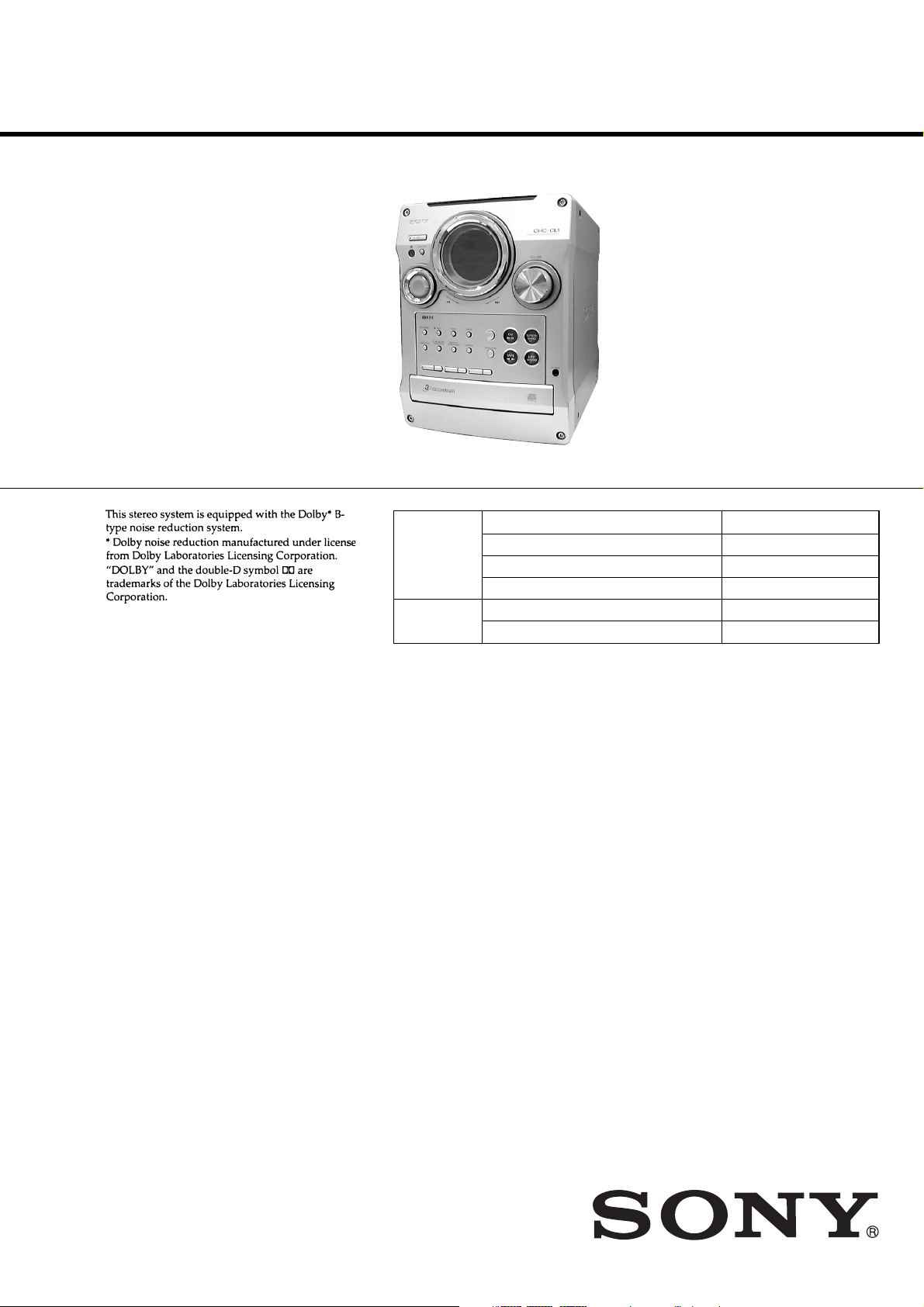
Photo : HCD-CL1
CD
SECTION
TAPE DECK
SECTION
Model Name Using Similar Mechanism HCD-DX50
CD Mechanism Type CDM63B
Base Unit Type BU-30BD60
Optical Pick-up Type A-MAX.3
Model Name Using Similar Mechanism HCD-CL5MD
Tape Transport Mechanism Type CMAL1Z215B
US Model
Australian Model
HCD-CL1
AEP Model
UK Model
E Model
HCD-CL1/CL3
SPECIFICATIONS
Amplifier section
For the U.S. model
AUDIO POWER SPECIFICATIONS
POWER OUTPUT AND TOTAL HARMONIC
DISTORTION:
With 6-ohm loads, both channels driven, from 120 –
10,000 Hz; rated 50 watts per channel minimum RMS
power, with no more than 10% total harmonic
distortion from 250 milli watts to rated output.
Total harmonic distortion: less than 0.1% (6 ohms at
AEP models
HCD-CL3:
DIN power output (Rated):80 + 80 watts
Continuous RMS power output (Reference):
Music power output (Reference):
HCD-CL1:
DIN power output (Rated):40 + 40 watts
Continuous RMS power output (Reference):
Music power output (Reference):
1 kHz, 25 W)
(6 ohms at 1 kHz, DIN)
100 + 100 watts
(6 ohms at 1 kHz, 10%
THD)
180 + 180 watts
(6 ohms at 1 kHz, 10%
THD)
(6 ohms at 1 kHz, DIN)
50 + 50 watts
(6 ohms at 1 kHz, 10%
THD)
95 + 95 watts
(6 ohms at 1 kHz, 10%
THD)
Other models
The following measured at AC 120/220/240 V, 50/
60 Hz
HCD-CL3:
DIN power output (Rated):80 + 80 watts
Continuous RMS power output (Reference):
HCD-CL1:
DIN power output (Rated):40 + 40 watts
Continuous RMS power output (Reference):
Inputs
MD IN (phono jacks): voltage 450 mV,
Outputs
CD DIGITAL OUT (Supported sampling
frequencies: 32 kHz, 44.1 kHz and 48 kHz)
PHONES (stereo minijack):
(6 ohms at 1 kHz, DIN)
100 + 100 watts
(6 ohms at 1 kHz, 10%
THD)
(6 ohms at 1 kHz, DIN)
50 + 50 watts
(6 ohms at 1 kHz, 10%
THD)
impedance 47 kilohms
accepts headphones of
8 ohms or more.
— Continued on next page —
COMPACT HiFi COMPONENT SYSTEM
9-873-852-13
2002J1600-1
© 2002.10
Sony Corporation
Home Audio Company
Published by Sony Engineering Corporation
Page 2
HCD-CL1/CL3
CD player section
System Compact disc and digital
Laser Semiconductor laser
Frequency response 2 Hz – 20 kHz (±0.5 dB)
Tape deck section
Recording system 4-track 2-channel stereo
Frequency response 40 – 13,000 Hz (±3 dB),
Tuner section
FM stereo, FM/AM superheterodyne tuner
FM tuner section
Tuning range 87.5 – 108.0 MHz
Antenna FM lead antenna
Antenna terminals 75 ohms unbalanced
Intermediate frequency 10.7 MHz
AM tuner section
Tuning range
AEP models: 531 – 1,602 kHz
Other models: 531 – 1,602 kHz
Antenna AM loop antenna
Intermediate frequency 450 kHz
General
Power requirements
North American model: 120 V AC, 60 Hz
AEP models: 230 V AC, 50/60 Hz
Australian and New Zealand models:
Mexican model: 120 V AC, 60 Hz
Korean model: 220 V AC, 60 Hz
Other models: 120 V, 220 V, 230 –
Power consumption
U.S.A. model:
HCD-CL1: 100 watts
AEP models:
HCD-CL3: 165 watts
HCD-CL1: 100 watts
HCD-CL3/CL1: 0.5 watts (at the Power
Other models:
HCD-CL3: 165 watts
HCD-CL1: 100 watts
Dimensions (w/h/d) incl. projecting parts and controls
Mass
Amplifier/Tuner/Tape/CD section:
HCD-CL3: Approx. 8.0 kg
HCD-CL1: Approx. 7.7 kg
Design and specifications are subject to change
without notice.
audio system
(λ=780 nm)
Emission duration:
continuous
using Sony TYPE I
cassettes
(50 kHz step)
(with the interval set at
9 kHz)
(with the interval set at
9 kHz)
530 – 1,710 kHz
(with the interval set at
10 kHz)
External antenna terminals
230 – 240 V AC, 50/
60 Hz
240 V AC, 50/60 Hz
Adjustable with voltage
selector
Saving Mode)
Approx. 215 × 285 ×
421 mm
SAFETY CHECK-OUT
After correcting the original service problem, perform the
following safety checks before releasing the set to the customer:
Check the antenna terminals, metal trim, “metallized” knobs, screws,
and all other exposed metal parts for A C leakage. Check leakage as
described below.
LEAKAGE
The AC leakage from any exposed metal part to earth ground
and from all exposed metal parts to any exposed metal part having
a return to chassis, must not exceed 0.5 mA (500 microamperes).
Leakage current can be measured by any one of three methods.
1. A commercial leakage tester, such as the Simpson 229 or RCA
WT -540A. Follo w the manufacturers’ instructions to use these
instruments.
2. A battery-operated AC milliammeter. The Data Precision 245
digital multimeter is suitable for this job.
3. Measuring the voltage drop across a resistor by means of a
VOM or battery-operated A C voltmeter . The “limit” indication
is 0.75 V, so analog meters must have an accurate low-v olta ge
scale. The Simpson 250 and Sanwa SH-63Trd are e xamples of
a passive VOM that is suitable. Nearly all battery operated
digital multimeters that have a 2V AC range are suitable. (See
Fig. A)
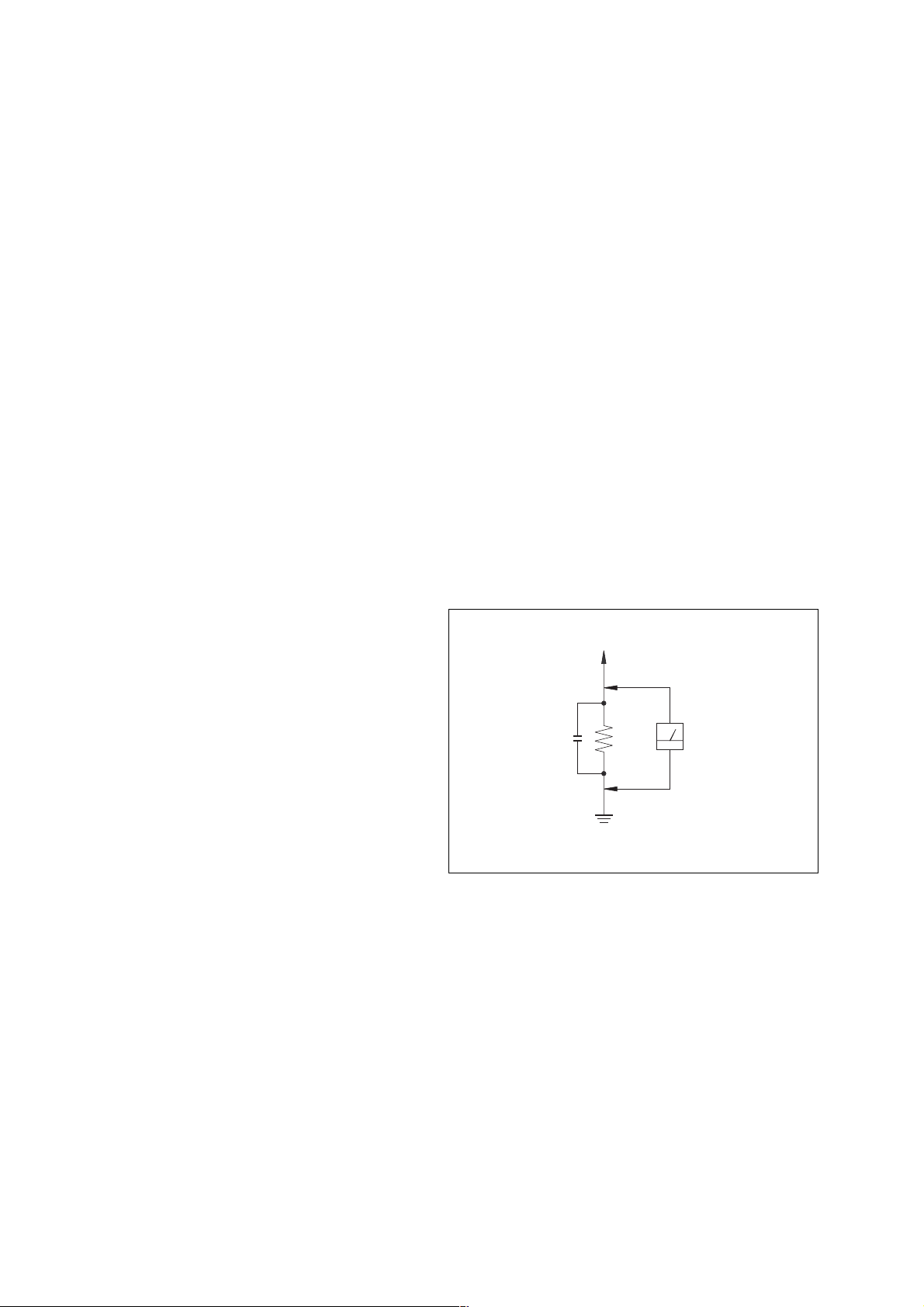
To Exposed Metal
Parts on Set
AC
0.15 µF
Fig. A. Using an AC voltmeter to check AC leakage.
1.5 kΩ
Earth Ground
Voltmeter
(0.75 V)
2
Page 3

TABLE OF CONTENTS
HCD-CL1/CL3
1. SERVICING NOTES ······················································· 4
2. GENERAL ·········································································· 5
3. DISASSEMBLY
3-1. Top Panel, Side Panel ···················································· 7
3-2. Cassette Mechanism ······················································ 8
3-3. Front Panel ···································································· 8
3-4. Panel Board ··································································· 9
3-5. Back Panel, Main Board················································ 9
3-6. Amp Board, Power Transformer ································· 10
3-7. CD Mechanism ···························································· 10
3-8. CD Base Unit (BU-30BD60) ······································ 11
3-9. Driver Board ································································ 12
3-10.Fitting Base (Stabilizer) Assy, Tray Assy, ··················· 12
3-11.Tray Sensor Board ······················································· 13
3-12.Slider (Loading), Gear (Slider) ··································· 13
3-13.Stocker Assy, Tray (Sub) ············································· 14
3-14.Disc Sensor Board ······················································· 14
3-15.IN OUT SW Board ······················································ 15
3-16.Motor Assy (M721), Motor Board ······························ 15
4. TEST MODE ···································································· 16
5. MECHANICAL ADJUSTMENTS ····························· 17
6. ELECTRICAL ADJUSTMENTS ·······························17
7. DIAGRAMS
7-1. Circuit Boards Location ·············································· 21
7-2. Block Diagrams CD Section ······································· 22
Syscon Section ···························································· 23
Main Section ······························································· 24
7-3. Printed Wiring Board Main Section ··························· 25
7-4. Schematic Diagram Main Section (1/2) ····················· 26
7-5. Schematic Diagram Main Section (2/2) ····················· 27
7-6. Schematic Diagram BD Section ································· 28
7-7. Printed Wiring Board BD Section ······························ 29
7-8. Schematic Diagram Driver Section ···························· 30
7-9. Printed Wiring Board Driver Section ························· 31
7-10.Schematic Diagram TC Section ································· 32
7-11.Printed Wiring Board TC Section······························· 33
7-12.Schematic Diagram AMP Section ······························34
7-13.Printed Wiring Board AMP Section ··························· 35
7-14.Schematic Diagram Panel Section ····························· 36
7-15.Printed Wiring Board Panel Section··························· 37
7-16.Schematic Diagram Trans Section ····························· 38
7-17.Printed Wiring Board Trans Section ··························· 39
7-18.Schematic Diagram Power Section ···························· 40
7-19.Printed Wiring Board Power Section ························· 41
7-20.IC Pin Function Description ········································ 42
7-21.IC Block Diagrams ······················································ 44
8. EXPLODED VIEWS
8-1. Side Panel, Back Panel Section ···································46
8-2. Front Panel Section ····················································· 48
8-3. Chassis Section ···························································· 49
8-4. CD Mechanism Deck Section-1 ·································· 50
8-5. CD Mechanism Deck Section-2 ·································· 51
8-6. Base Unit Section (BU-30BD60) ································ 52
9. ELECTRICAL PARTS LIST ······································· 53
3
Page 4
HCD-CL1/CL3
SECTION 1
SERVICING NOTES
NOTES ON HANDLING THE OPTICAL PICK-UP
BLOCK OR BASE UNIT
The laser diode in the optical pick-up block may suffer electrostatic
break-down because of the potential difference generated by the
charged electrostatic load, etc. on clothing and the human body.
During repair, pay attention to electrostatic break-down and also
use the procedure in the printed matter which is included in the
repair parts.
The flexible board is easily damaged and should be handled with
care.
NOTES ON LASER DIODE EMISSION CHECK
The laser beam on this model is concentrated so as to be focused on
the disc reflective surface by the objective lens in the optical pickup block. Therefore, when checking the laser diode emission,
observe from more than 30 cm away from the objective lens.
Laser component in this product is capable
of emitting radiation exceeding the limit for
Class 1.
This appliance is classified as a CLASS 1 LASER product. The
CLASS 1 LASER PRODUCT MARKING is located on the rear
exterior.
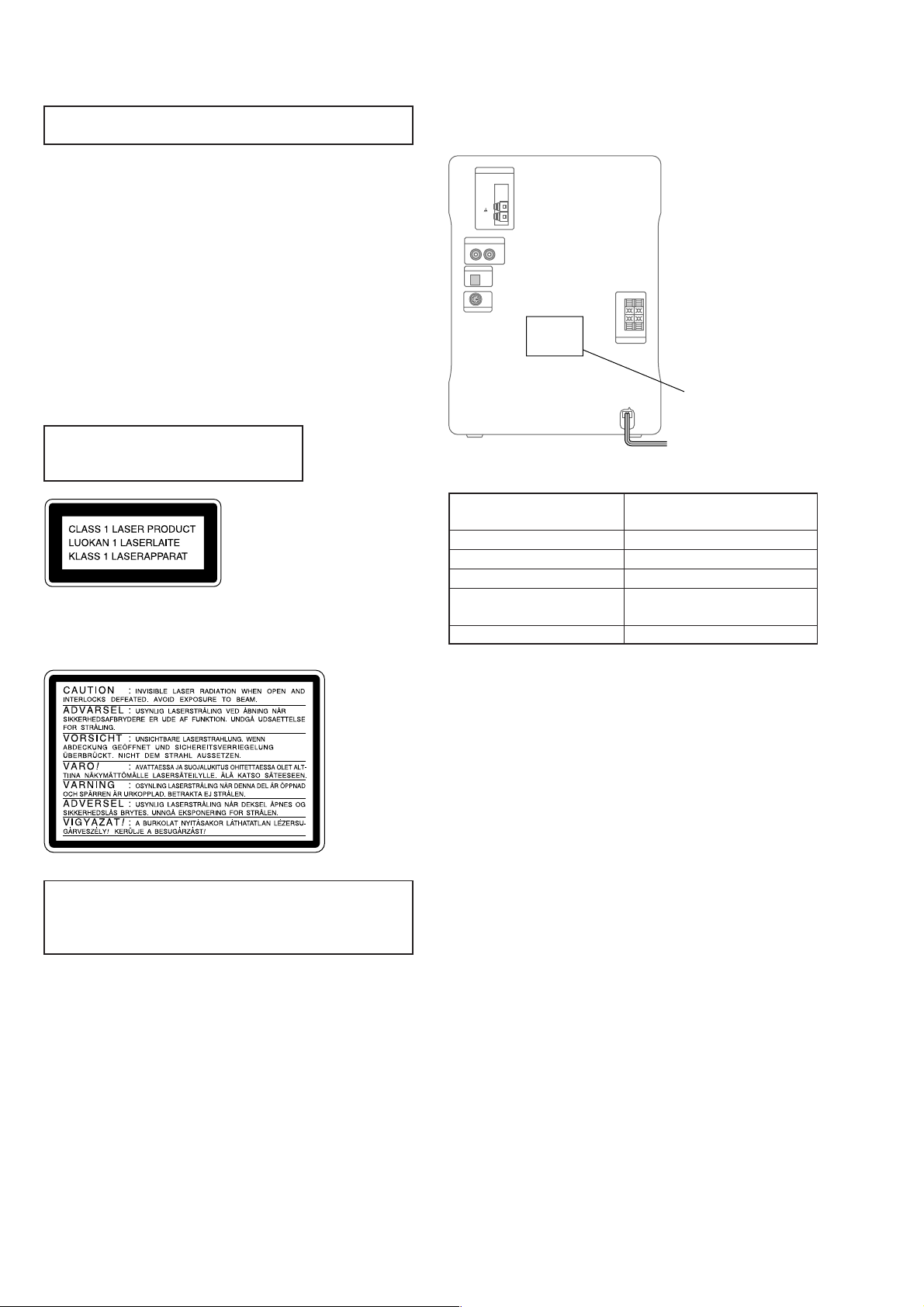
MODEL IDENTIFICATION
– Back Panel –
Model
US, Mexican models
AEP, UK models
Australian model
E, Taiwan models
Korea model
Power Voltage
Indicator
Power Voltage
Incdication
AC: 120 V 60 Hz
AC: 230 V 50/60 Hz
AC: 230 – 240V 50/60 Hz
AC: 110, 220/
230 – 240 V 50/60 Hz
AC: 220 V 60 Hz
This caution
label is
located inside
the unit.
CAUTION
Use of controls or adjustments or performance of procedures
other than those specified herein may result in hazardous radiation
exposure.
Notes on chip component replacement
• Never reuse a disconnected chip component.
• Notice that the minus side of a tantalum capacitor may be
damaged by heat.
Flexible Circuit Board Repairing
• Keep the temperature of soldering iron around 270˚C
during repairing.
• Do not touch the soldering iron on the same conductor of the
circuit board (within 3 times).
• Be careful not to apply force on the conductor when soldering
or unsoldering.
SAFETY-RELATED COMPONENT WARNING!!
COMPONENTS IDENTIFIED BY MARK 0 OR DOTTED LINE WITH
MARK 0 ON THE SCHEMATIC DIAGRAMS AND IN THE PARTS
LIST ARE CRITICAL TO SAFE OPERATION. REPLACE THESE
COMPONENTS WITH SONY PARTS WHOSE PART NUMBERS
APPEAR AS SHOWN IN THIS MANUAL OR IN SUPPLEMENTS
PUBLISHED BY SONY.
4
Page 5
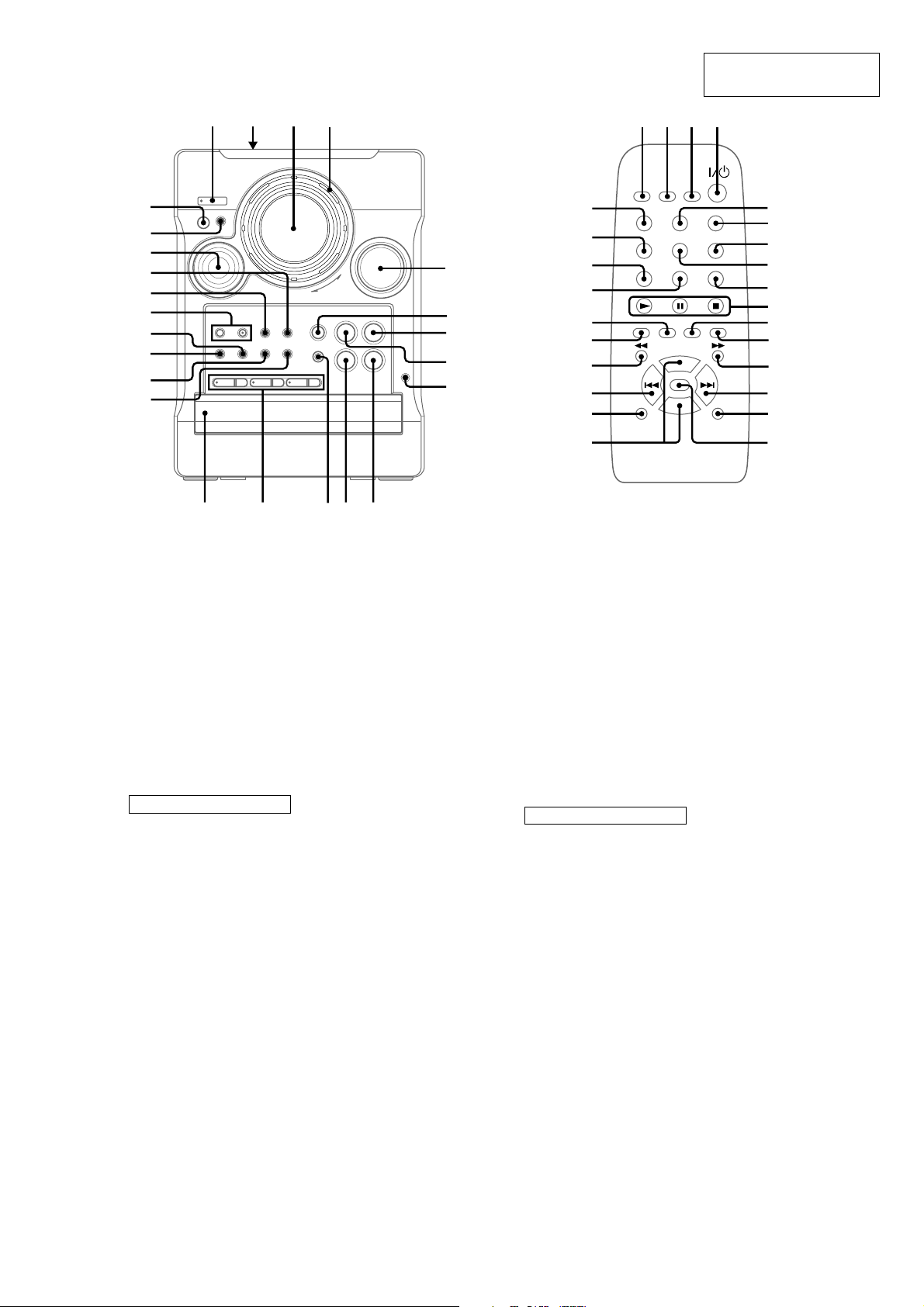
wf
6
7
8
9
5
qf
qg
qh
0
qd
qa
qs
ql
qk
qj
w;
1234
wa
ws
wd
wh
wg
wf
CHECK 8 (11)
CLEAR qs (11)
CLOCK/TIMER SELECT 2
(20, 23)
CLOCK/TIMER SET 3
(8, 19, 22)
DBFB wh (20)
DIMMER wd (7)
DISC SKIP 9 (10, 12)
DISPLAY qk (8, 12)
ENTER/YES qa (8, 13, 14, 19,
22)
FUNCTION qg (9, 17, 18)
GROOVE qh (20)
MENU/NO wa (14)
MUSIC MENU 6 (21)
NAME EDIT/CHARACTER ws
(12, 16)
REPEAT 7 (10)
SCROLL wg (13)
SLEEP 1 (22)
SURROUND 5 (20)
TUNER/BAND wf (14, 15)
VOL +/– qj
BUTTON DESCRIPTIONS
@/1 4
N q;
x q;
X q;
M qd
> qf
. ql
m w;
wd
ws
wa
w;
ql
qk
qj
qh
qg
1234
SECTION 2
GENERAL
5
6
7
8
9
HCD-CL1/CL3
This section is extracted
from instruction manual.
BASS/TREBLE ws (21)
CD 1 – 3 qd (11)
CD 1 – 3 Z qd (9)
CD disc tray qf (9)
CD SYNC ql (18)
CD NX 8 (9)
DBFB wa (20)
DIMMER qg (7)
DISPLAY wd (8, 12)
Display window 3
EDIT w; (18)
FUNCTION qs (9, 17, 18 )
GROOVE qj (20)
MD 0 (24)
MUSIC MENU ws (21)
BUTTON DESCRIPTIONS
?/1 1
./> 4
x 6
m/M ws
+/– ws
PHONES jack 9
PLAY MODE/DIRECTION qk
(9, 17, 18)
REC PAUSE/START ql (18, 19)
Remote sensor wf
REPEAT qh (10)
STEREO/MONO qh (15)
Tape deck lid 2 (17)
TAPE nN qa (17, 18)
TUNER/BAND 7 (14, 15)
VOLUME 5
0qaqsqdqf
5
Page 6

HCD-CL1/CL3
Setting the time
1
Turn on the system.
2
Press CLOCK/TIMER SET on the
remote.
Proceed to step 5 when you set the clock for
the first time.
3
Turn ./> (or press . or > on
the remote) to select “CLOCK SET?”.
4
Press ENTER/YES.
5
Turn ./> (or press . or > on
the remote) to set the hour.
6
Press M (or ENTER/YES on the
remote).
The minute indication flashes.
7
Turn ./> (or press . or > on
the remote) to set the minute.
8
Press ENTER/YES on the remote.
The clock starts working.
If you made a mistake
Press m or M repeatedly until the incorrect
item flashes, then set it again.
To change the preset time
Start over from step 1.
Saving the power in
standby mode
Press DISPLAY repeatedly when the
system is off. Each time you press the
button, the system switches cyclically as
follows:
Demonstration t Clock display t Power
Saving Mode
To cancel the Power Saving Mode
Press DISPLAY once to show the
demonstration, twice to show the clock display.
Tip
?/1 indicator lights up even in the Power Saving
Mode.
6
Page 7
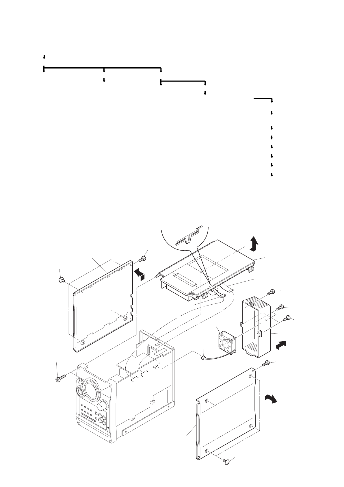
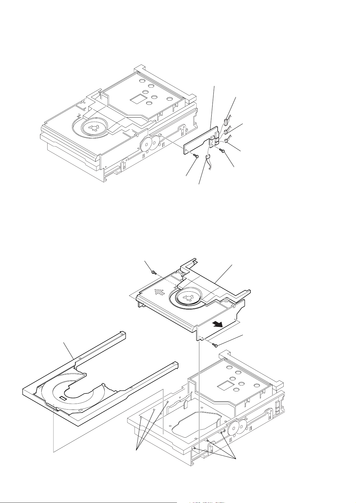
SECTION 3
DISASSEMBLY
• The equipment can be removed using the following procedure.
Set
Top panel, Side panel
HCD-CL1/CL3
Cassette mechanism Front panel
Panel board
Back panel, Main board
Amp board,
Power transformer
Note : Follow the disassembly procedure in the numerical order given.
3-1. TOP PANEL, SIDE PANEL
Note: Attach it so that it pressed down
the Main board.
q;
qs
Side panel (L)
(Remove in the direction
of the arrow)
qa
Four screws
(
CASE 3 TP2)
qd
Two screws
HEXAGON
(
SOCKET TAPPING
)
Screw
+BVTT 3 × 8
(
)
qg
Connector
(CN305)
CD mechanism
CD base unit (BU-30BD60)
6
D.C. Fan
3
Connector
(CN904)
Driver board
Fitting base (stabilizer) assy,
Tray assy
Tray sensor board
Slider (loading), Gear (slider)
Stocker assy
Disc sensor board
IN OUT SW board
Motor assy (M721), Motor board
qh
Top panel
(Remove in the direction
of the arrow)
qf
Flat cable (9 core)
(CN304)
1
Screw
(
+BVTT 3 × 8
5
Two screws
(
+BVTP 3 × 8
2
Two screws
+BVTP 3 × 8
(
4 Heat sink, cover
7
Screw
+BVTT 3 × 8
(
)
)
)
)
9
Side panel (R)
(Remove in the direction
of the arrow)
8
Four screws
CASE 3 TP2)
(
7
Page 8
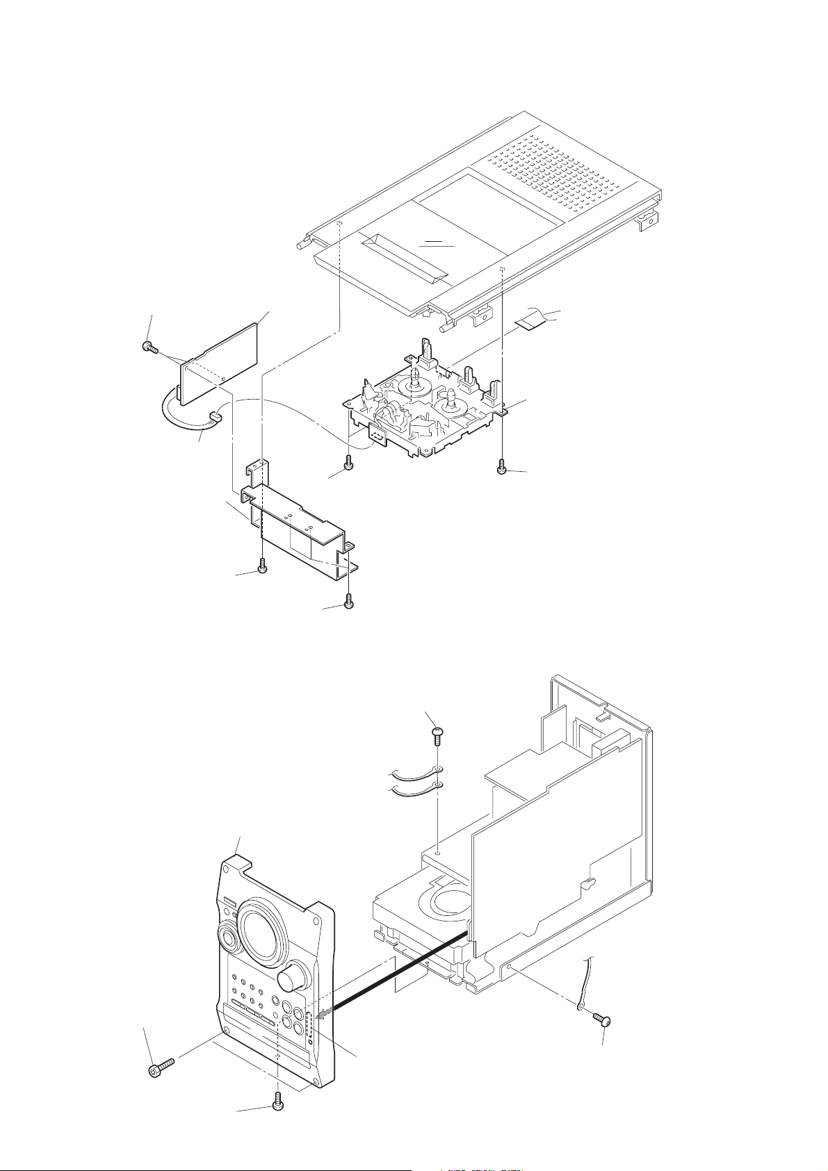
HCD-CL1/CL3
k
3-2. CASSETTE MECHANISM
4
Two screws
+BVTP 3 × 8
(
5
TC board
)
7
Flat cable (9 core)
8
Cassette mechanism dec
3
Bracket
(Cassette mechanism)
2 S
(
3-3. FRONT PANEL
1
Connector
crew
+BVTP 2.6 × 8
)
2 Three s
+BVTP 2.6 × 8
(
6
Front panel
6
Two screws
+BVTP 2.6 × 8
(
crews
6
Screw
+BVTP 2.6 × 8
)
)
1
Screw
(
+BVTP 3 × 8
)
(
)
4
Two screws
(
HEXAGON
SOCKET TAPPING
3
(
)
Screw
+BVTP 3 × 8
2
5
Connector
(CN701)
)
Screw
(
+BVTP 3 × 8
)
8
Page 9

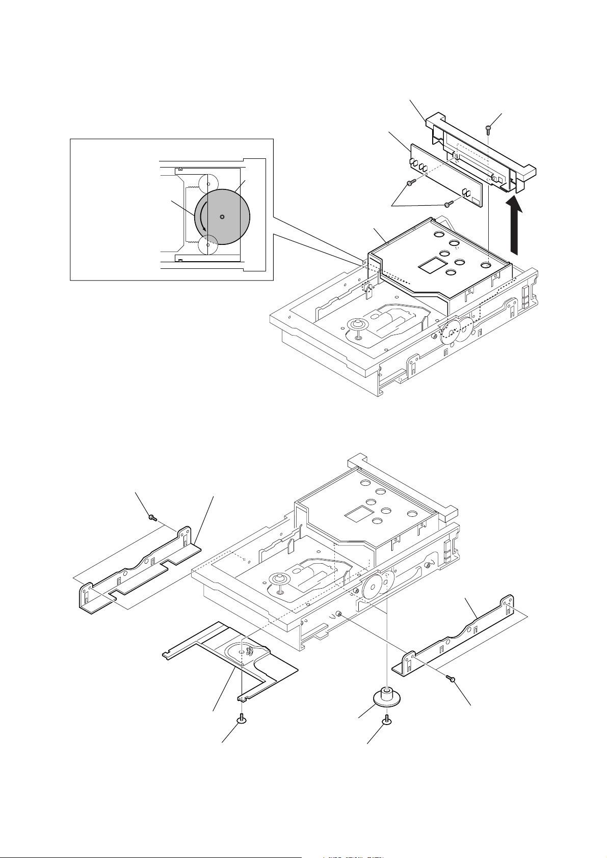
3-4. PANEL BOARD
2
Nut
5
Panel board
6
Two screws
(+BVTP 2.6
×
4
(
8)
Six screws
+BVTP 2.6 × 8
7
Ring SW board
)
3
(
Four screws
+BVTP 2.6 × 8
)
4
Eight screws
+BVTP 2.6 × 8
(
HCD-CL1/CL3
)
1
Knob (vol)
3-5. BACK PANEL, MAIN BOARD
8
(CN943)
9
Connector
(CN942)
0
Connector
Main board
(CN941)
qs
5
Connector
Vol sel board
Back panel
qa
Two screws
(
+BVTP 3 × 8
)
3
Screw
(
+BVTP 3 × 8
6
(
2
Connector
(CN803)
1
Flat cable (15 core)
(CN502)
4 Thirteen
(
+BVTP 3 × 8
Two screws
+BVTP 3 × 8
)
7
Tuner
screws
)
)
qj
Connector
(CN201)
qg
Connector
(CN501)
qf
Connector
(CN701)
qk
Main board
qh
Two connector
(CN101, CN251)
qd
Two screws
(
+BVTP 3 × 8
)
9
Page 10
HCD-CL1/CL3
3-6. AMP BOARD, POWER TRANSFORMER
3
Four screws
(+BVTP 4
4
Power
transformer
2
Connector
(CN902)
×
8)
6
Three screws
(
+BVTP 3 × 8
1
Connector
(CN901)
5
Two screws
(
+BVTP 3 × 16
)
)
8
(+BVTP 3
Two screws
7
Amp board
×
9
8)
q;
Two screws
(
+BVTP 3 × 8
Heat sink
qs
Cord bushing
)
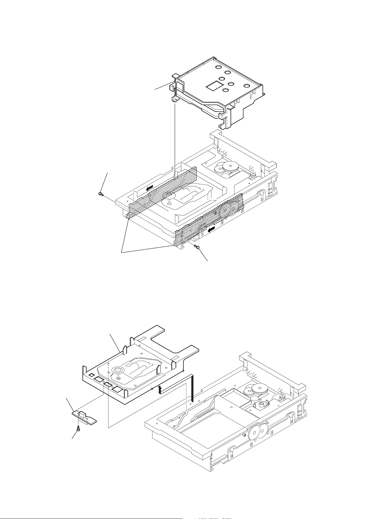
3-7. CD MECHANISM
5
CD mechanism deck
(CDM63B)
qa
Sub power board
3 Chassis assy
4
(
10
2
Two screws
(
+BVTP 3 × 8)
Four screws
+BVTP 3 × 8
1
Three screws
(
+BVTP 3 × 8
)
Note: When installing the CD mechanism, the four bosses
must be aligned with the specified positions.
)
Page 11
3-8. CD BASE UNIT (BU-30BD60)
)
HCD-CL1/CL3
0
CD base unit
(BU-30BD60)
8
Two insulators
6
Two stoppers
5
Two screws (+BVTP 2.6
4
BD board
1
Rivet
×
9
Two insulators
7 Two
screws (+PTPWH M2.6
8)
3
Flat type wire (16 core)
2
Flat type wire (21 core)
11
Page 12
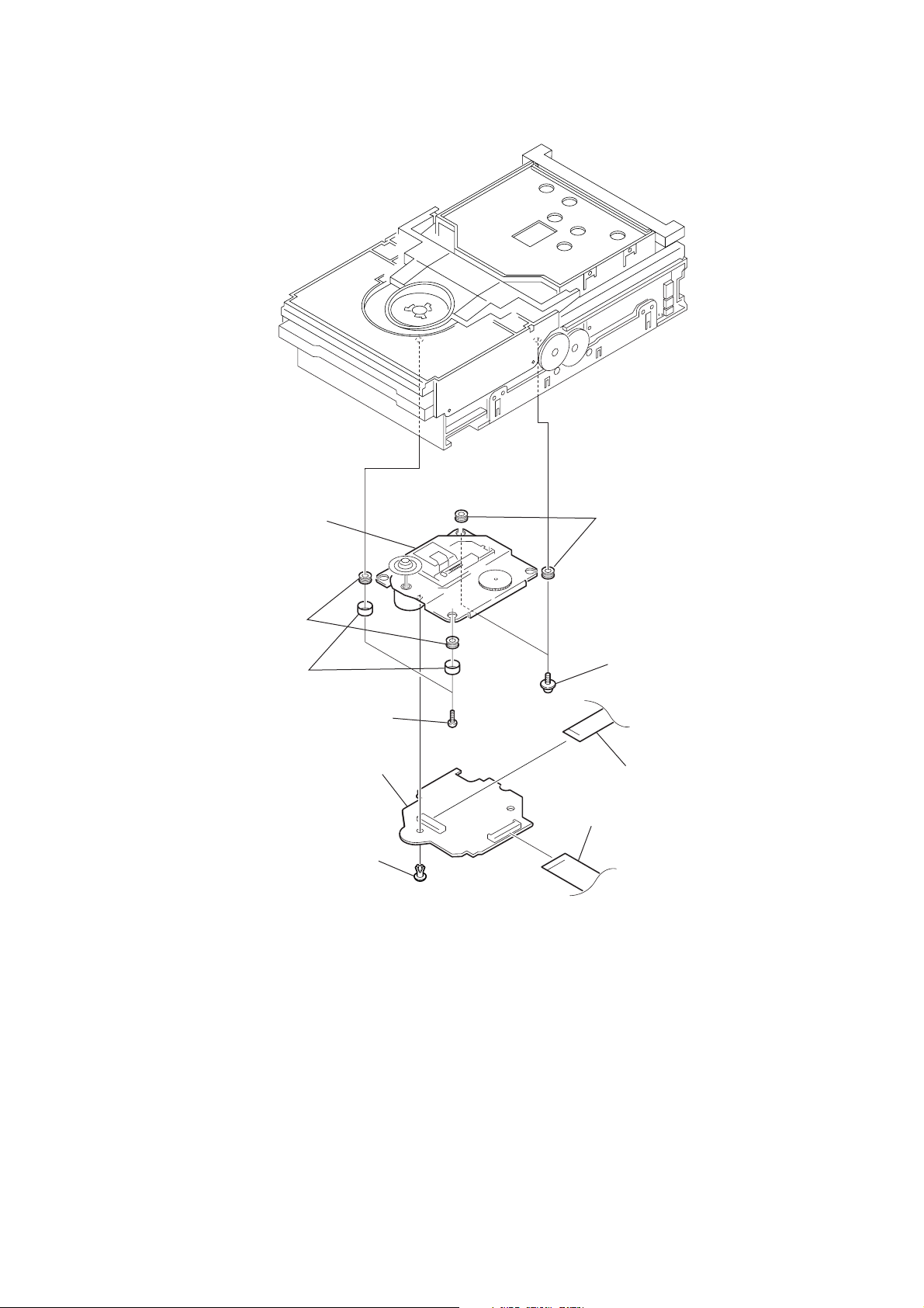
HCD-CL1/CL3
3-9. DRIVER BOARD
3 DRIVER board
1 Connector (CN703)
1 Connector (CN704)
1 Connector (CN702)
2 Screw (BTTP M2.6)
2 Screw (BTTP M2.6)
1 Connector (CN705)
3-10. FITTING BASE (STABILIZER) ASSY, TRAY ASSY
1 Two screws (BTTP M2.6)
2
5 Tray assy
4 Fitting base (STABILIZER) assy
2
1 Two screws (+BTTP M2.6)
12
3 Three bosses
3 Three bosses
Page 13
3-11. TRAY SENSOR BOARD
1 Rotate the cam,
and lift up the stocker
at the full.
HCD-CL1/CL3
6 HOLDER (SENSOR)
2 Two screws (+BTTP M2.6)
5 TRAY SENSOR board
Cam
4 Two screws (+BTTP M2.6)
3-12. SLIDER (LOADING), GEAR (SLIDER)
3 Two screws (+BTTP M2.6)
4 Bracket (retainer)
Stocker
3
6 Slider (LOADING)
5 Floating screw
2 Bracket (retainer)
1 Two screws (+BTTP M2.6)
8 Two gears (SLIDER)
7 Two floating screw
13
Page 14
HCD-CL1/CL3
3-13. STOCKER ASSY, TRAY (SUB)
1 Screw (+BTTP M2.6)
3 Stoscker assy
A
2 Slide the slider (BU.L),
slider (BU.R) in the direction of
arrow A at the full.
3-14. DISC SENSOR BOARD
2 CD base unit assy
4 DISC SENSOR board
A
1 Screw (+BTTP M2.6)
1
14
3 Two screws (+BTTP M2.6)
Page 15
3-15. IN OUT SW BOARD
HCD-CL1/CL3
2 Two screws (+BTTP M2.6)
3 IN OUT SW board
1 Connector (CN704)
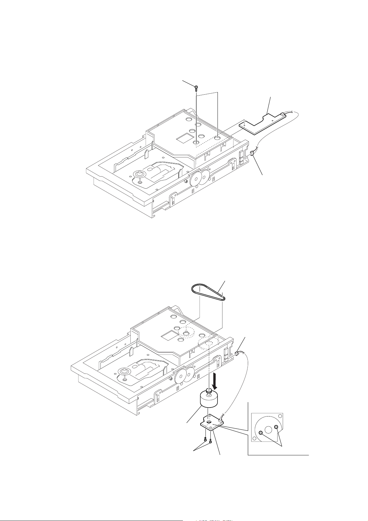
3-16. MOTOR ASSY (M721), MOTOR BOARD
7 Motor assy (M721)
1 Belt
2 Connector (CN702)
6
Motor board bottom view
4 Two screws (+BTTP M2.6)
3 Remove two solders.
5 Motor board
15
Page 16

HCD-CL1/CL3
SECTION 4
TEST MODE
[CD Ship Mode]
• This mode moves the optical pick-up to the position durable to
vibration. Use this mode when returning the set to the customer
after repair.
Procedure:
1. Press ?/1 button to turn the set ON.
2. Press CD 1 button and FUNCTION button simultaneously.
3. After the “STANDBY” display blinks six times, a message
“LOCK” is displayed on the fluorescent indicator tube, and the
CD ship mode is set.
[GC Test Mode]
• This mode is used to check the software version, FL tube, LED,
keyboard and VACS.
Procedure:
1. Press three buttons x , DISPLAY , and CD 2 simultaneously.
2. LEDs and fluorescent indicator tube are all turned on.
3. When you want to enter the software version display mode,
press CD 1 . The model number and destination are displayed.
4. Each time CD 1 is pressed, the display changes starting from
MC version, GC version, CD version, CDD version, CDM version, BD version, ST version, TA version, TM version, TC version and MD version in this order.
5. Press CD 2 button, and the key check mode is activated.
6. In the key check mode, the fluorescent indicator tube displays
“K 0 J 0 V 0”. Each time a button is pressed, “K 0” value
increases. However, once a button is pressed, it is no longer
taken into account.
“V 0” value increases like 1, 2, 3 ... if rotating VOLUME knob
in “+” direction, or it decreases like 0, 9, 8 ... if rotating in
“–” direction.
7. Also when CD 3 is pressed after lighting of all LEDs and FL
tubes, value of VACS appears.
8. To exit from this mode, press three buttons in the same manner
as step 1, or disconnect the power cord.
[MC Test Mode]
• This mode is used to check operations of the respective sections
of Amplifier, Tuner, CD and Tape.
Procedure:
1. Press the ?/1 button to turn on the set.
2. Press the three buttons of x , DISPLAY and CD 3 simulta-
neously.
3. The “VOLUME” segment flashes.
4. Every pressing of BASS/TREBLE f changes the displays in
the order of
“GEQ MIN”t“GEQ FLAT”t“GEQ MAX”
5. When the VOLUME control knob is turned clockwise even
slightly, the sound volume increases to its maximum and a message “VOLUME MAX” appears for two seconds, then the display returns to the original display.
6. When the VOLUME control knob is turned counter-clockwise
even slightly, the sound volume decreases to its minimum and a
message “VOLUME MIN” appears for two seconds, then the
display returns to the original display.
7. In the test mode, the default-preset channel is called even when
the TUNER is selected and an attempt is made to call the preset
channel that has been stored in memory, by operating the Shuttle
knob. (It means that the memory is cleared.)
8. When a tape is inserted in Deck and recording is started, the
input source function selects MD automatically.
9. When x button is pressed to stop recording, the Tape (Deck) is
selected and tape is rewound using the m button, tape is rewound, tape is stops at around the record-starting position and
playback of the recorded portion of the tape is started. If PAUSE
is inserted even once during recording, tape is rewound to the
position around the PAUSE position and is played back.
10.The cold reset is enforced at the same time.
[CD Service Mode]
• This mode can run the CD sled motor freely. Use this mode, for
instance, when cleaning the optical pick-up.
Procedure:
1. Press ?/1 button to turn the set ON.
2. Select the function “CD”.
3. Press three buttons x , FUNCTION , and CD 2 simultaneously.
4. The CD service mode is selected.
5. With the CD in stop status, turn the shuttle knob clockwise to
move the optical pick-up to outside track, or turn the shuttle
knob counter-clockwise to inside track.
6. To exit from this mode, perform as follows:
1) Move the optical pick-up to the most inside track.
2) Press three buttons in the same manner as step 2.
Note: • Always move the optical pick-up to most inside track when exit-
ing from this mode. Otherwise, a disc will not be unloaded.
• Do not run the sled motor excessively, otherwise the gear can be
chipped.
[CD Ship (Memory Clear) Mode]
• Set the CD ship mode and set the default setup when shipped
from the factory at the next AC power on.
Procedure:
1. Press ?/1 button to turn the set ON.
2. Select the function “CD ”.
3. Press three buttons x , FUNCTION and CD 1 simulta-
neously.
4. After the “STANDBY” display blinks six times, a message
“LOCK” is displayed on the fluorescent indicator tube, and the
CD ship mode is set.
[CD/TAPE Repeat 5 Times Limit Release Mode]
• 5 times limit of repeating CD/TAPE is released.
Procedure:
1. Press ?/1 button to turn the set ON.
2. Press three buttons x , FUNCTION and CD 1Z .
3. 5 times limit of repeating CD/TAPE is released.
4. Cold reset is performed at power off.
16
Page 17
SECTION 5
MECHANICAL ADJUSTMENTS
HCD-CL1/CL3
SECTION 6
ELECTRICAL ADJUSTMENTS
Precaution
1. Clean the following parts with a denatured alcohol-moistened
swab:
record/playback heads pinch rollers
erase head rubber belts
capstan idlers
2. Demagnetize the record/playback head with a head demagnetizer.
3. Do not use a magnetized screwdriver for the adjustments.
4. After the adjustments, apply suitable locking compound to the
parts adjusted.
5. The adjustments should be performed with the rated power supply voltage unless otherwise noted.
Torque Measurement
Mode
FWD
FWD
back tension
REV
REV
back tension
FF/REW
FWD tension
REV tension
Torque meter Meter reading
3.04 – 6.96 N • m
CQ-102C
CQ-102C
CQ-102RC
CQ-102RC
CQ-201B
CQ-403A
CQ-403R
(31 to 71 g • cm)
(0.43 – 0.98 oz • inch)
0.20 – 0.58 N • m
(2 to 6 g • cm)
(0.02 – 0.08 oz • inch)
3.04 – 6.96 N • m
(31 to 71 g • cm)
(0.43 – 0.98 oz • inch)
0.20 – 0.58 N • m
(2 to 6 g • cm)
(0.02 – 0.08 oz • inch)
6.97 – 14.02 N • m
(71 to 143 g • cm)
(0.98 – 1.99 oz • inch)
0.98 N • m or more
(100 g or more)
(3.53 oz or more)
0.98 N • m or more
(100 g or more)
(3.53 oz or more)
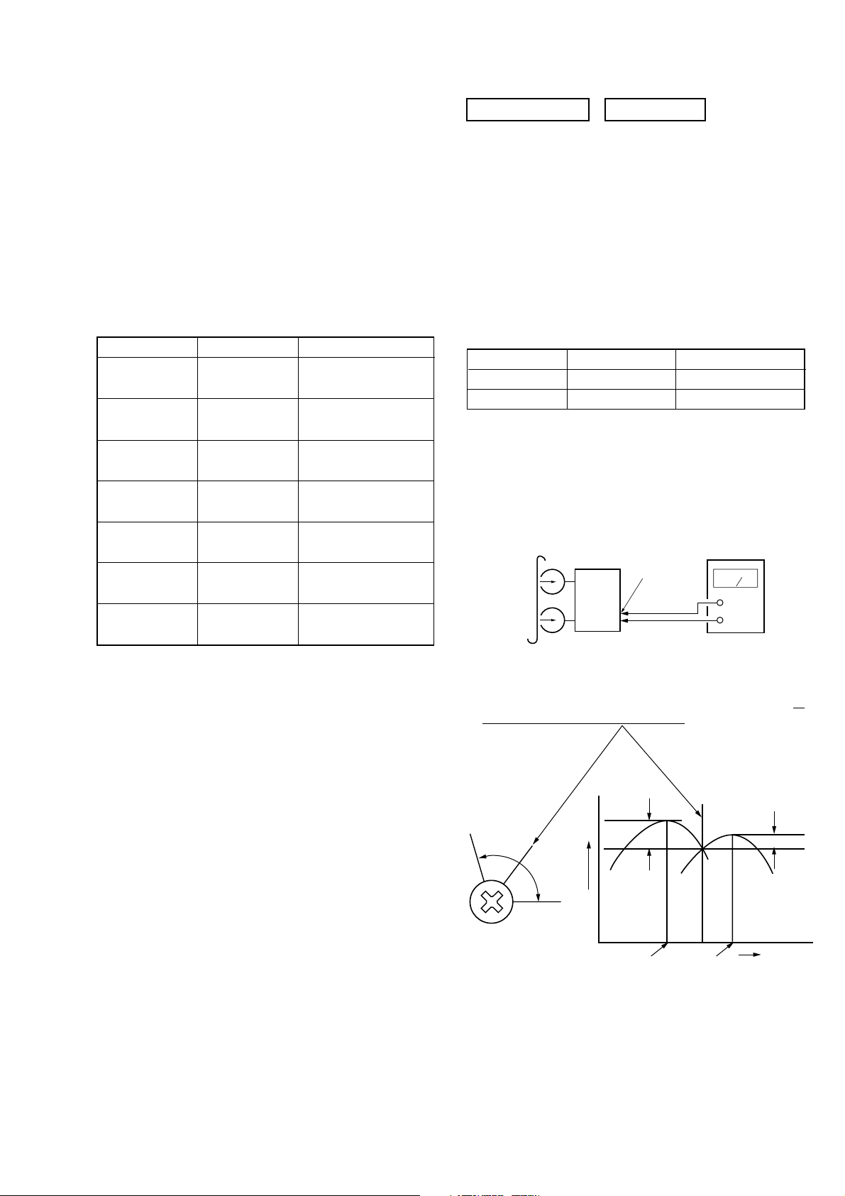
DECK SECTION 0 dB=0.775V
1. Demagnetize the record/playback head with a head demagnetizer.
2. Do not use a magnetized screwdriver for the adjustments.
3. After the adjustments, apply suitable locking compound to the
parts adjusted.
4. The adjustments should be performed with the rated power supply voltage unless otherwise noted.
5. The adjustments should be performed in the order given in this
service manual. (As a general rule, playback circuit adjustment
should be completed before performing recording circuit adjustment.)
6. The adjustments should be performed for both L-CH and R-CH.
7. Switches and controls should be set as follows unless otherwise
specified.
Signal Used forTape
P-4-A100
WS-48B
Record/Playback Head Azimuth Adjustment
Procedure:
1. Mode : Playback
test tape
P-4-A100
(10kHz, –10dB)
10 kHz, –10 dB
3 kHz, 0 dB
main board
CN301
Pin 1 (L-ch)
Pin 3 (R-ch)
set
Azimuth Adjustment
Tape Speed Adjustment
level meter
+
–
2. Turn the adjustment screw and check output peaks. If the peaks
do not match for L-CH and R-CH, turn the adjustment screw
that outputs match within 1 dB of peak.
L-CH
peak
screw
position
R-CH
peak
output
level
within
1 dB
L-CH
peak
R-CH
peak
within 1dB
screw
position
so
17
Page 18
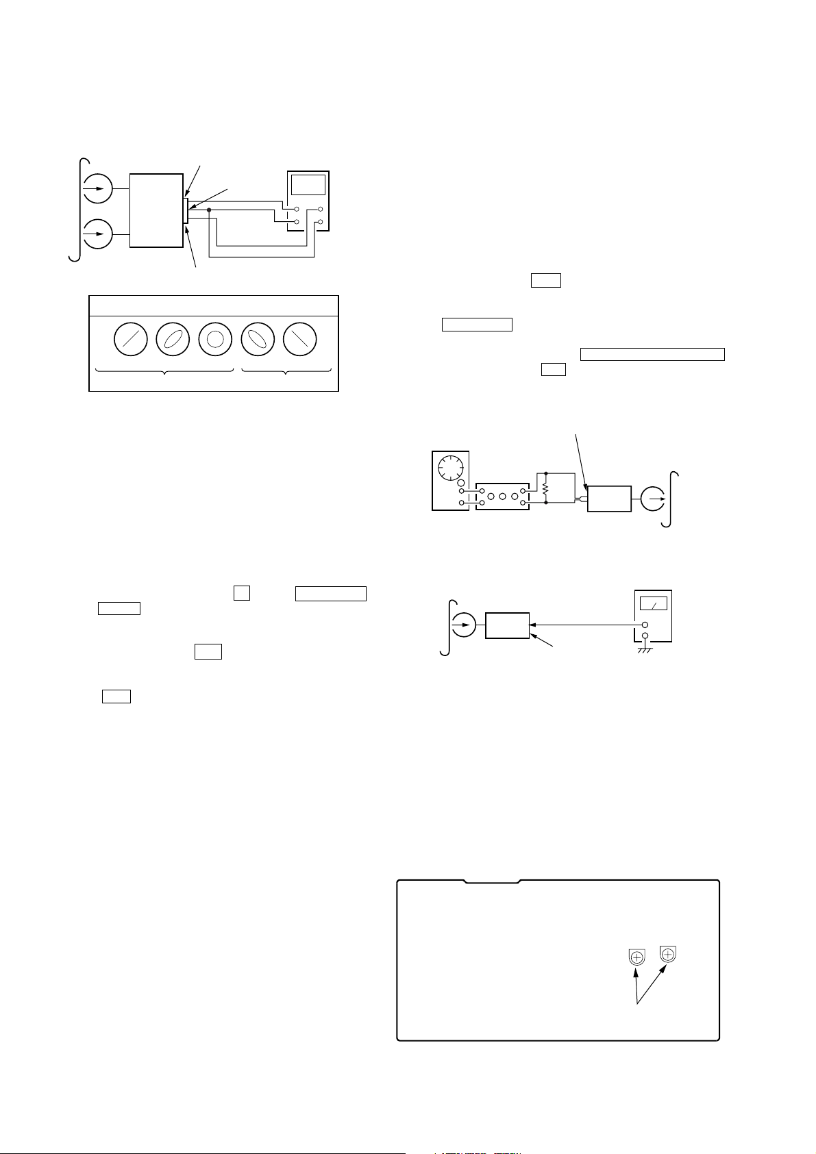
HCD-CL1/CL3
e
3. Mode: Playback
test tape
P-4-A100
(10kHz, –10dB)
set
in phase 45°
main board
CN301
Pin 1 (L-ch)
Pin 2 (GND)
L
R
Pin 3 (R-ch)
Waveform of oscilloscope
90°
good
135°
oscilloscope
180°
wrong
4. After the adjustments, apply suitable locking compound to the
parts adjusted.
Adjustment Location: Record/Playback/Erase Head
Tape Speed Check
Record Bias Adjustment
Procedure:
INTRODUCTION
When set to the test mode performed in Tape Speed Adjustment, when the tape is rewound after recording, the “REC memory
mode” which rewinds only the recorded portion and playback is
set.
This “REC memory mode” is convenient for performing this ad-
justment. During recording, the input signal FUNCTION will automatically switch to VIDEO.
(After recording, press the m button without stopping will return to the position where recording was started.)
1. Press FUNCTION button to select VIDEO. (This step is not
necessary if the above test mode has already been set.)
2. Insert a tape into deck, press the TAPE REC PAUSE/START
button, and then press the Y button to start recording.
3. Mode: Record
VIDEO (AUDIO) IN
1) 315 Hz
2) 10 kHz
AF OSC
attenuator
600 Ω
} 50 mV (–23.8 dB)
blank tap
CS-123
set
Note: Set the test mode using the following method and begin tape
speed adjustment.
Procedure:
With the power turned ON, press the x button, ENTER/YES
button, and DISC 3 button simultaneously.
(The “VOLUME” on the fluorescent display tube will blink while
in the test mode.)
To exit the test mode, press the "/1 button.
1. Insert the WS-48B into deck.
2. Press the Y button of deck.
3. Check the reading of frequency counter becomes 3000 ± 15 Hz.
Sample Value of Wow and flutter
W.RMS (JIS) less than 0.3%
(test tape: WS-48B)
4. Mode: Playback
recorded
position
set
main board
CN301
Pin 3 (L-ch)
Pin 1 (R-ch)
level meter
5. Confirm playback the signal recorded in step 2 become adjustment level as follows.
If these levels do not adjustment lev el, adjust the R V304 (L-CH)
and RV354 (R-CH) on the TC board to repeat steps 3 and 4.
Adjustment level: The playback output of 10 kHz le vel dif ference
against 315 Hz reference should be 0 ± 0.5 dB.
Adjustment Location:
[TC BOARD]
18
RV304
RV304(Lch),RV354(Rch)
Record Bias
RV354
Page 19
HCD-CL1/CL3
e
TP(RFAC)
BD (CD) board
oscilloscope
TP(DVC)
Record Level Adjustment
Procedure:
INTRODUCTION
When set to the test mode performed in Tape Speed Adjustment, when the tape is rewound after recording, the “REC memory
mode” which rewinds only the recorded portion and playback is
set.
This “REC memory mode” is convenient for performing this
adjustment. During recording, the input signal FUNCTION will automatically switch to VIDEO.
(After recording, press the m button without stopping will return to the position where recording was started.)
1. Press FUNCTION button to select VIDEO. (This step is not
necessary if the above test mode has already been set.)
2. Insert a tape into deck, press the TAPE REC PAUSE/START
button, and then press the Y button to start recording.
3. Mode: Record
VIDEO (AUDIO) IN (J101)
315Hz 50 mV (–23.8 dB)
AF OSC
600 Ω
attenuator
set
blank tap
CS-123
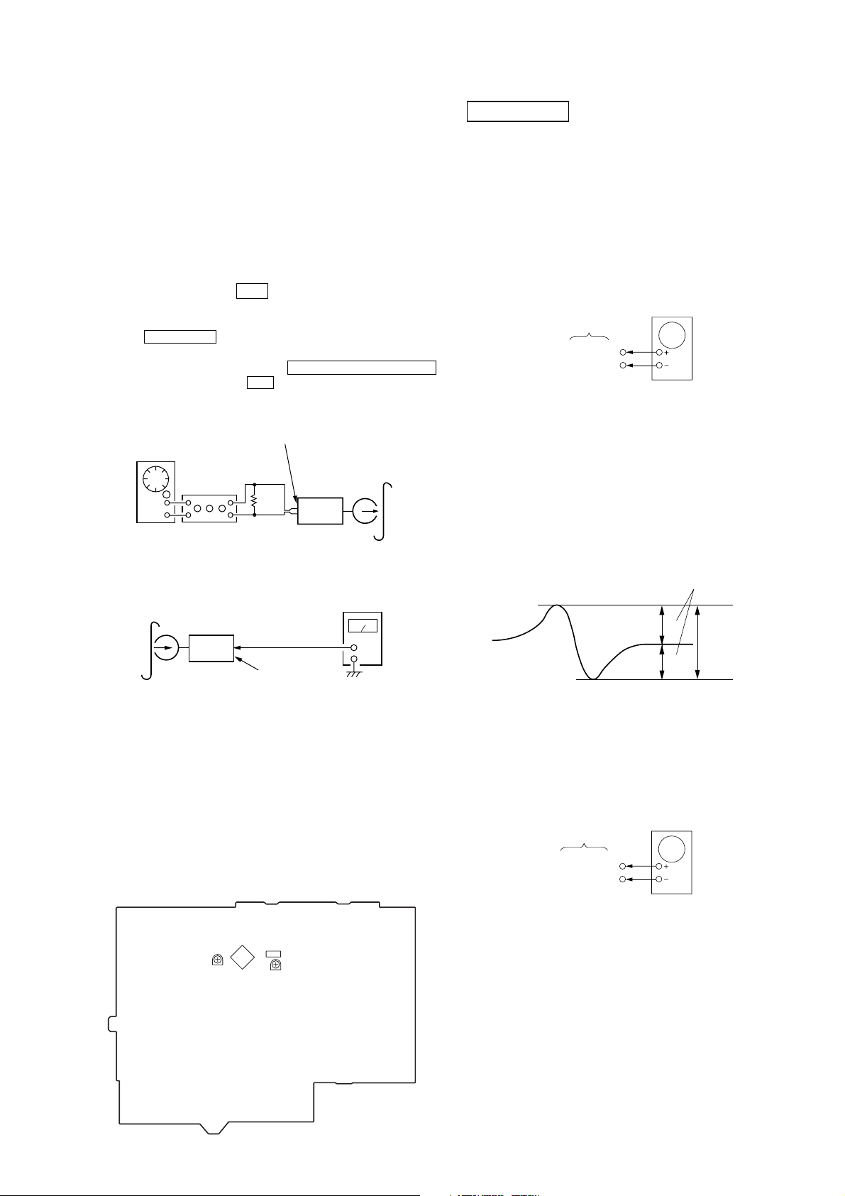
CD SECTION
Note :
1. CD Block is basically designed to operate without adjustment.
Therefore, check each item in order given.
2. Use LUV-P01 (4-999-032-01) unless otherwise indicated.
3. Use an oscilloscope with more than 10MΩ impedance.
4. Clean the object lens by an applicator with neutral detergent
when the signal level is low than specified value with the following checks.
S-Curve Check
Oscilloscope
BD (CD) board
TP(FEO)
TP(DVC)
Procedure :
1. Connect an oscilloscope to TP (FEO).
2. Connect between TP (FEI) and TP (DVC) ( 1.65 V) by lead
wire.
3. Turn Power switch on.
4. Load a disc (LUV -P01) and actuate the focus search. (In consequence of open and close the disc tray, actuate the focus search)
5. Confirm that the oscilloscope waveform (S-curve) is symmetrical between A and B. And conf irm peak to peak level within 2 ±
0.5 Vp-p.
4. Mode: Playback
recorded
position
set
main board
CN301
Pin 3 (L-ch)
Pin 1 (R-ch)
level meter
5. Confirm playback the signal recorded in step 2 become adjustment level as follows.
If these levels do not adjustment le vel, adjust the R V301 (L-CH)
and R V351 (R-CH) on the MAIN board to repeat steps 3 and 4.
Adjustment level:
CN301 playback level: 47.2 to 53.0 mV (–24.3 to –23.3 dB)
Adjustment Location:
[MAIN BOARD]
IC301
CN301
Record Level (R ch)
RV351
RV301
Record Level (L ch)
S-curve waveform
symmetry
A
within 2 ±0.5Vp-p
B
6. After check, remove the lead wire connected in step 2.
Note : • Try to measure several times to make sure than the ratio
of A : B or B : A is more than 10 : 7.
• Take sweep time as long as possible and light up the
brightness to obtain best waveform.
RF Level Check
Procedure :
1. Connect an oscilloscope CH1 to TP (RFDC) and CH2 to TP
(RFAC).
2. Turn Power switch on.
3. Load a disc (LUV-P01) and playback.
4. Confirm that oscilloscope waveform is clear and check if RF
signal level is correct or not.
19
Page 20
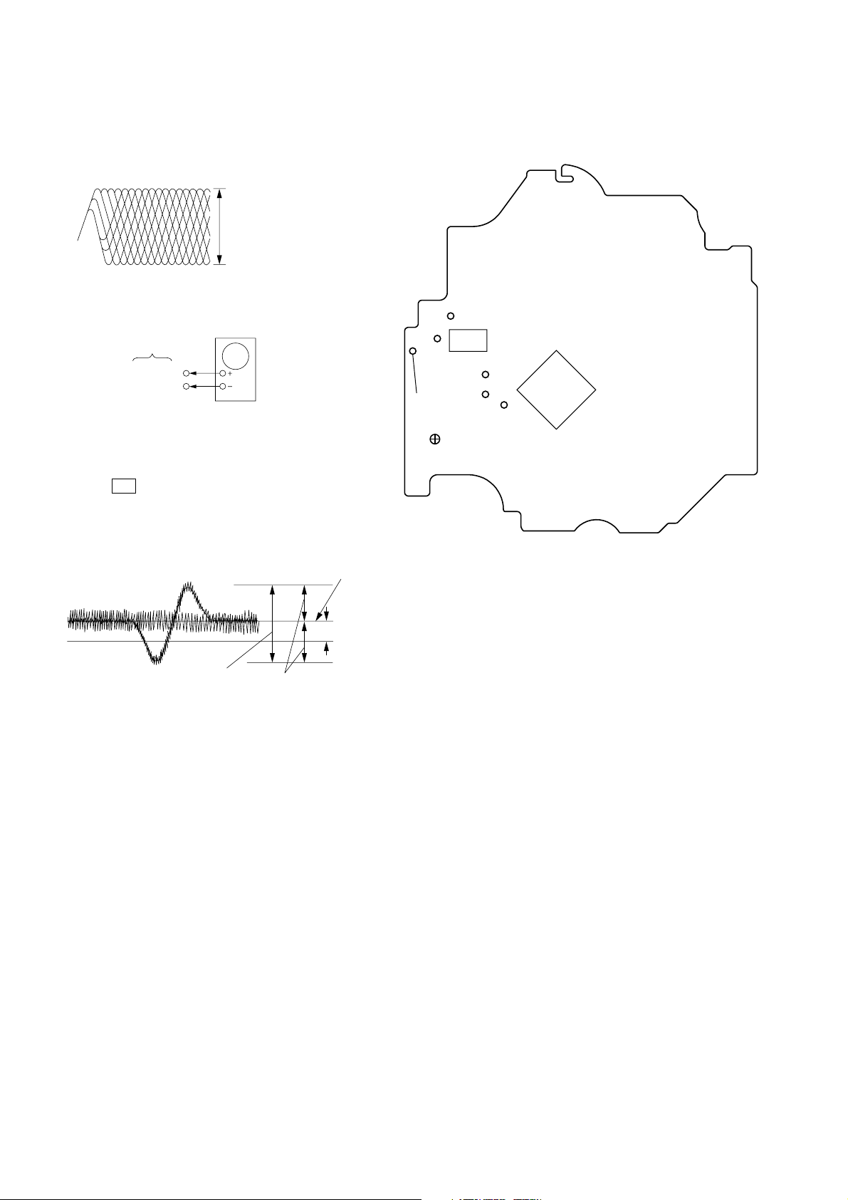
HCD-CL1/CL3
e
)
Note : Clear RF signal waveform means that the shape “ ◊ ” can be clearly
distinguished at the center of the waveform.
RF signal waveform
VOLT/DIV : 200mV
TIME/DIV : 500ns
level : 0.65 ±0.15Vp-p (RFDC)
1.1 ±0.4Vp-p (RFAC)
E-F Balance (1 Track jump) Check
oscilloscop
BD (CD) board
TP(TEO)
TP(DVC)
Procedure :
1. Connect an oscilloscope to TP (TEO) and TP (DVC).
2. Turn Power switch on.
3. Load a disc (LUV-P01) and playback the number nine track.
4. Press the gG button. (Becomes the 1 track jump mode.)
5. Confirm that the level B and A (DC voltage) on the oscilloscope waveform.
Adjustment Location:
[BD (CD) BOARD] (Conductor Side)
TP (DVC)
TP
15
IC103
16
1
30
TP
(RFDC)
40
41
IC101
60
2021
80
61
(RFAC)
TP
(FEI)
RV101
TP (FEO)
TP (TEO)
1
1 track jump waveform
DVC
level=1.0 ±0.5Vp-p
B
symmetry
center of
waveform
A (DC voltage
6. Adjust RV101 on the BD board so that the center of waveform
becomes the same voltage of DVC. (i.e. A=0V)
20
Page 21

SECTION 7
DIAGRAMS
HCD-CL1/CL3
7-1. CIRCUIT BOARDS LOCATION
TC board
BACK LIGHT board
RING SW board
PANEL board
TRANS board
VOL SEL board
THERMAL board
MAIN board
AMP board
THIS NOTE IS COMMON FOR PRINTED WIRING
BOARDS AND SCHEMATIC DIAGRAMS.
(In addition to this, the necessary note is printed
in each block.)
For schematic diagrams.
Note:
• All capacitors are in µF unless otherwise noted. pF: µµF
50 WV or less are not indicated except for electrolytics
and tantalums.
• All resistors are in Ω and
specified.
f
•
• 2 : nonflammable resistor.
• 1 : fusible resistor.
• C : panel designation.
Note: The components identified by mark 0 or dotted line
• A : B+ Line.
• B : B– Line.
• H : adjustment for repair.
• Voltages and waveforms are dc with respect to ground
• Voltages are taken with a VOM (Input impedance 10 MΩ).
• Waveforms are taken with a oscilloscope.
• Circled numbers refer to waveforms.
• Signal path.
• Abbreviation
: internal component.
with mark 0 are critical for safety.
Replace only with part number specified.
under no-signal (detuned) conditions.
Voltage variations may be noted due to normal production tolerances.
Voltage variations may be noted due to normal production tolerances.
F : FM
E : PB
a : REC
J : CD (Analog)
c : CD (Digital)
AUS : Australian model
MX : Mexican model
TW : Taiwan model
KR : Korea model
1
4
/
W or less unless otherwise
• Indication of transistor
B
CE
B
CE
C
Q
B
E
These are omitted.
These are omitted.
These are omitted.
TRAY SENSOR board
IN OUT SW board
DISK SENSOR board
BD (CD) board
MOTOR board
DRIVER board
SUB POWER board
For printed wiring boards.
Note:
• X : parts extracted from the component side.
• Y : parts extracted from the conductor side.
a
•
• : Pattern from the side which enables seeing.
Caution:
Pattern face side: Parts on the pattern face side seen from the
(Side B) pattern face are indicated.
Parts face side: Parts on the parts face side seen from the
(Side A) parts face are indicated.
: Through hole.
2121
Page 22

HCD-CL1/CL3
7-2. BLOCK DIAGRAMS
CD SECTION
• Signal Path
: CD
OPTICAL PICK-UP
BLOCK
(A-MAX.3)
VC
VCC
PD1
PD2
I5-10
I1-6
LD
GND
PD
VR
SW
F+
F-
+5V
Q101
LD
DRIVE
IC103
RF AMP
27
VC
25
VFC
6
7
8
9
10
11
1
2
MOTOR/COIL DRIVE
14
CH1FO
13
CH1RO
A
B
C
D
E
F
LD
PD
RFAC
RFDCO
RFDCI
IC102
CH1RI
SW
FEI
CH1FI
15
28
16FE
18TE
12
17
29
IC101
DIGITAL SERVO
DIGITAL SIGNAL PROCESSOR
D/A CONVERTER
D OUT
60
51
RFAC
43
RFDC
39
FE
41
TE
40
SE
27 SSTP
2
3
32
33
FFDR
FRDR
L OUT
R OUT
DATA
CLOK
XLAT
SQSO
SENS
SCLK
SQCK
SCOR
72
75
20
5
7
6
3
1
8
9
2
R-CH
DATA
CLK
XLT
CD-L
11 10
4
5
A
IC504
1
98
6
SECTION
MAIN
2
DIGITAL
(OPTICAL)
13
IC551
OUT
12
IC401(1/3)
MASTER CONTROL
35
CD-DATA
37
CD-CLK
42
XLT
32
SQ-DATA-IN
36
SENS
33
SQ-CLK
19
SCOR
:DIGITAL OUT (OPTICAL)
T+
12
CH2FO
T-
M102
SLED
MOTOR
M101
SPINDLE
MOTOR
M
M
11
17
18
15
16
CH2RO
CH3FO
CH3RO
CH4FO
CH4RO
CH2FI
CH2RI
CH3FI
CH3RI
CH4SI
MUTING
5
6
24
23
25 MDP
20
30
31
28
29
26
TFDR
TRDR
SFDR
SRDR
XTAI
XTAO
XRST
66
67
X101
16.9344MHz
3
LDON
XRST
PWM1
PWM2
PWM3
41
LDON
43
XRST
28
BU PWM 1
26
BU PWM 2
24
BU PWM 3
+3.3V
Q102,D101
+3.3V
REG.
+5V
2222
Page 23

SYSCON SECTION
IC401(2/3)
MASTER CONTROL
XC-IN
XC-OUT
HCD-CL1/CL3
IC702
REMOTE
SENSOR
10
11
X401
32.768kHz
S701
2
4
SIRCS
POWER KEY
74
+5V
LCD
+5V
VREF
TC-MECHA
PLAY SW
SENSOR OUT
BTRGM+
+5V
R REC
F REC
PACK
M 9V
(TC-LID-SW)
Q396-397
MOTOR
CONTROL
Q391-392
TRIGGER
MOTOR
CONTROL
S501
91
55
57
90
53
60
B HALF/REC
CAPM-CNT1
B PLAY
B-SHUT
B TRG
TC LID
X-IN
X-OUT
15
13
X402
16MHz
S707
DISPLAY
VOLUME
S791
RING
SW
SUB TRAY 1
HEIGHT SENSOR
SUB TRAY 2
HEIGHT SENSOR
SUB TRAY 3
HEIGHT SENSOR
S742
(OUT)
S706
ROTARY
ENCODER
S741-746
FUNCTION
KEY
S718-724
FUNCTION
KEY
S711-717
S747-750
FUNCTION
KEY
IC731
IC732
IC733
73
DISPLAY KEY
79
VOL A
78
VOL B
97
KEY0
95
KEY1
94
KEY2
48
T-SENS1
49
T-SENS2
50
T-SENS3
46
OPEN
LCD DATA
LCD SCK
LCD STB
STB LED
BACK LIGHT
LED 1
LED 2
LED 3
LED 4
5
7
6
39
77
89
1
2
3
DATA
SCK
STB
Q746
DRIVER
Q745
DRIVER
Q744
DRIVER
Q701
DRIVER
Q702
DRIVER
LED
LED
LED
LED
LED
DATA
SCK
STB
D701
(POWER)
CL1: D771-776
CL3: D777-779
(BACK LIGHT)
+5v
Q741-743
D741 D743 D745 D712
CD1 CD2 CD3
TAPE
•REC
(DISC IN DETECT)
S741
(IN)
IC751
CLOSE
47
IC701
LOADING MOTOR DRIVER
Q701
52
LOAD-OUT
DISC-SENS
LOAD-IN
45
44
9
RIN
FIN
7
OUT1
OUT2
4
2
M
M721
(LOADING)
2323
Page 24

HCD-CL1/CL3
MAIN SECTION
REC/PB HEAD
ERASE HEAD
IC201
SOUND PROCESSOR
J101
36
37
38
39
D+5V
EQ IN(L)
VIDEO
CDMD
TC
ST
38
IC501
RESET
RV301
REC LEVEL
CLK
22 21 20
31
IC301
DOLBY NR
DOLBY NR
39
OUT
INBB
NFBB
FBB
REC
DATA
LATCH
PAS
REC OUT(L)
33
25
26
27
28
35
REC-L
DOL
DOLBY
TYPE B
BIAS SW
Q203
MUTING
Q201
SWITCH
28
27
MS
LM ON/ OFF
BIAS ON/OFF
RM ON/OFF
ALC ON/OFF
+
Q183
SWITCH
MS OUT
PB OUT(L)
PB
R LIN(L)
R-CH
Q181,182
SWITCH
26
40
25
24
43
20
22
15
+
Q501
RESET
SWITCH
R-CH
AEP,UK
FEEDBACK
MASTER CONTROL
FRONT-RELAY
84
71
LINE MUTING
67
DA-MUTING
100
AC CUT
12
RESET
82
AMP-LAT
81
AMP-DATA
83
AMP-CLK
27
ST-CLK
25
ST-D IN
23
ST-D OUT
22
ST-CE
88
TUNED
87
STEREO
21
ST-MUTING
20
RDS-DATA
18
RDS-INT
AMS-IN
54
58
TC-MUTING
59
R/PB/PASS
65
BIAS
61
REC MUTING
68
ALC
TC-RELAY
69
IC401 (3/3)
STK-POWER
DBFB ON/OFF
HEAD PHONE
STBY-RELAY
L
VIDEO
(AUDIO)
IN
CD
SECTION
R
A
R-CH
CD-L
TUNER UNIT
ST-L
ST-R
ST-CLK
ST-D OUT
ST-D IN
ST-CE
TUNED
STEREO
ST MUTING
RDS-DATA
RDS-INT
IC304
+A
L
R
X
R-CH
IC302
3
P
ERASE BIAS
1
R
REC/PB
4
75
RV304
REC
BIAS
T301
REC BIAS
R-CH
A IN(L)
48
46
B IN(L)
EQ OUT(L)
36
Q302,303
BIAS
OSC
AEP,UK
+10V
16
PB-A/B
+12V
Q301
POWER AMP
15
14
Q971-973
PROTECT
DETECT
CD-POWER
IC801
+
–
12
MUTING
SWITCH
72
40
86
70
38
80
10
11
Q271
SWITCH
Q834
SWITCH
CD +5V
Q801
OVERLOAD
DET.
Q835
DRIVER
E +5V
THP842
Q841,842
THERMAL
DET.
Q831-833
PROTECT
SWITCH
Q106,109
B+
SWITCH
D +5V
Q881,882
RELAY
DRIVER
Q836-837
PROTECT
DC AMP
POWER AMP
D108
+10V
Q104
REG.
A +9V
M +7V
Q911
RELAY
DRIVER
+5.7V
RY801
+B
-B
IC105
+5.7V
3 1
REG.
IC101
+10V
3 1
REG.
IC102
+9V
3 1
REG.
IC103
+7V
3 1
REG.
IC911
+5.7V
3 1
REG.
Q931-933
R-CH
D961
D962
R-CH
FAN
DRIVER
D901
D953-956
D957-960
RY911
D912-914
TM801
L
R
CL3
(FAN)
T901
POWER
TRANSFORMER
T911
SUB
TRANSFORMER
SPEAKER
J701
PHONES
240V
220V
120V
• R-CH is omitted due to same as L-CH.
• Signal Path
: FM
: CD
: PB
: REC
• Abbreviation
AUS : Australian model
MX : Mexican model
TW : Taiwan model
KR : Korea model
CL1:
AUS
CL1:KR/CL3:KR
CL1:
E,TW
S943-1
EXCEPT
CL1:E,TW
CL1:
E,TW
EXCEPT
CL1:E,TW
CL1:
E,TW
CL1:
S943-2
E,TW
EXCEPT
CL1:E,TW
AC IN
2424
Page 25

HCD-CL1/CL3
7-3. PRINTED WIRING BOARD MAIN SECTION
(Page 41)
IC501
IC401
• See page 21 for Circuit Boards Location.
(Page 33)
IC301
IC504
There are a few cases that the part printed on
this diagram isn’t mounted in this model.
IC201
• Semiconductor
Location
Ref. No. Location
D103 G-4
D106 F-6
D107 F-8
D108 F-8
D182 F-11
D202 C-10
D203 C-11
D501 D-1
D502 B-1
D504 B-2
D505 B-2
D506 B-1
D507 B-1
D508 B-2
D509 B-2
D514 B-1
IC101 G-10
IC102 G-10
IC103 G-9
IC105 F-8
IC201 C-10
IC301 D-6
IC401 D-3
IC501 C-1
IC504 E-4
IC551 F-13
(Page 37)
IC 502
IC 503
IC110
IC 108
IC105
IC103 IC102 IC101
(Page 35)
IC 552
IC551
Q104 G-10
Q106 F-7
Q109 F-9
Q181 F-11
Q182 F-11
Q183 F-11
Q201 D-9
Q203 C-9
Q251 B-9
Q253 C-9
Q271 D-9
Q391 B-7
Q392 B-7
Q396 B-8
Q397 B-8
Q501 D-1
( )
(Page 29)
(Page 31)
(Page 35)
2525
Page 26

HCD-CL1/CL3
7-4. SCHEMATIC DIAGRAM MAIN SECTION (1/2)
• See page 45 for IC Block Diagram.
IC B/D
2626
Page 27

HCD-CL1/CL3
7-5. SCHEMATIC DIAGRAM MAIN SECTION (2/2)
• See page 42 for Waveforms.
• See page 42 for IC Pin Function Description.
2727
Page 28

HCD-CL1/CL3
7-6. SCHEMATIC DIAGRAM BD SECTION
• See page 42 for Wavefoms.
• See page 44 for IC Block Diagram.
I
(Page 27)
IC B/D
2828
Page 29

HCD-CL1/CL3
7-7. PRINTED WIRING BOARD BD SECTION
IC102
• See page 21 for Circuit Boards Location.
I
(Page 25)
There are a few cases that the part printed on
this diagram isn’t mounted in this model.
(A-MAX.3)
IC103
IC101
• Semiconductor
Location
Ref. No. Location
D101 B-3
IC101 C-3
IC102 B-2
IC103 D-2
Q101 C-1
Q102 A-3
2929
Page 30

HCD-CL1/CL3
7-8. SCHEMATIC DIAGRAM DRIVER SECTION
• See page 45 for IC Block Diagram.
IC B/D
27
3030
Page 31

HCD-CL1/CL3
7-9. PRINTED WIRING BOARD DRIVER SECTION
IC731
IC732
• See page 21 for Circuit Boards Location.
There are a few cases that the part printed on
this diagram isn’t mounted in this model.
IC733
IC751
IC701
K
TO
MAIN
BOARD
(Page 25)
3131
Page 32

HCD-CL1/CL3
7-10. SCHEMATIC DIAGRAM TC SECTION
• See page 45 for IC Block Diagram.
26
IC B/D
3232
Page 33

HCD-CL1/CL3
7-11. PRINTED WIRING BOARD TC SECTION
• See page 21 for Circuit Boards Location.
IC302
There are a few cases that the part printed on
this diagram isn’t mounted in this model.
(Page 25)
• Semiconductor
Location
Ref. No. Location
IC302 A-3
IC304 B-1
Q301 A-4
Q302 C-3
Q303 B-4
Q304 B-2
Q305 B-2
IC304
3333
Page 34

HCD-CL1/CL3
7-12. SCHEMATIC DIAGRAM AMP SECTION
3434
Page 35

HCD-CL1/CL3
7-13. PRINTED WIRING BOARD AMP SECTION
• See page 21 for Circuit Boards Location.
There are a few cases that the part printed on
this diagram isn’t mounted in this model.
(Page 25) (Page 39)
(Page 25)
• Semiconductor
Location
Ref. No. Location
D801 E-6
D831 B-7
D851 F-6
D881 H-5
D891 F-6
D953 B-2
D954 B-2
D955 B-2
D956 B-2
D957 B-2
D958 A-2
D959 B-2
D960 B-2
D961 B-3
D962 B-3
D971 D-7
D991 H-6
(Page 39)
IC801 F-8
Q801 E-6
Q831 D-5
Q832 C-5
Q833 C-5
Q834 C-5
Q835 D-5
Q836 E-5
Q837 E-5
Q841 B-7
Q842 B-7
Q851 F-6
Q881 G-5
Q882 F-5
Q971 D-7
Q972 C-7
Q973 C-7
IC801
3535
Page 36

HCD-CL1/CL3
7-14. SCHEMATIC DIAGRAM PANEL SECTION
3636
Page 37

HCD-CL1/CL3
7-15. PRINTED WIRING BOARD PANEL SECTION
• See page 21 for Circuit Boards Location.
There are a few cases that the part printed on
this diagram isn’t mounted in this model.
IC 702
• Semiconductor
Location
Ref. No. Location
D701 B-8
D702 E-4
D703 E-4
D712 G-6
D741 H-7
D743 H-6
D745 H-5
D746 E-8
D771 B-5
D772 C-5
D773 B-5
D774 C-5
D775 B-5
D776 B-4
D777 B-4
D778 B-5
D779 C-5
(Page 25)
DBFB
EDIT
REC
CD
SYNC
IC702 C-8
Q701 B-7
Q702 B-2
Q741 F-8
Q742 F-6
Q743 F-8
Q744 E-7
Q745 F-7
Q746 F-7
VIDEO
3737
Page 38

HCD-CL1/CL3
7-16. SCHEMATIC DIAGRAM TRANS SECTION
EXCEPT
CL1:AUS,KR/CL3:KR
CL1:AUSCL1:AUS
CL1:
JW6 JW7
3838
Page 39

HCD-CL1/CL3
7-17. PRINTED WIRING BOARD TRANS SECTION
(Page 35)
• See page 21 for Circuit Boards Location.
There are a few cases that the part printed on
this diagram isn’t mounted in this model.
(Page 35)
TO
SUB POWER BOARD
VOL SEL BOARD
(Page 41)
3939
Page 40

HCD-CL1/CL3
7-18. SCHEMATIC DIAGRAM POWER SECTION
EXCEPT
CL1:E,TW
EXCEPT
CL1:E,TW
CL1:
E,TW
EXCEPT CL1:E,TW
CL1:
E,TW
CL1:
E,TW
EXCEPT
CL1:E,TW
CL1:E,TW
4040
Page 41

HCD-CL1/CL3
7-19. PRINTED WIRING BOARD POWER SECTION
• See page 21 for Circuit Boards Location.
There are a few cases that the part printed on
this diagram isn’t mounted in this model.
• Semiconductor
Location
Ref. No. Location
D911 C-4
D912 A-4
D913 A-4
D914 A-4
D915 A-4
IC911 B-4
Q911 C-5
IC911
(Page 39)
VOLTAGE
(Page 25)
E, Taiwan models
SELECTOR
4141
Page 42

HCD-CL1/CL3
• WAVEFORMS
– BD (CD) SECTION –– MAIN SECTION –
1
1
IC101 ta
(RFAC)(CD Play mode)
1.1 Vp-p
2
IC101 ra
(TE)(CD Play mode)
0.4 Vp-p
3
IC101 el
(FE)(CD Play mode)
4
IC101 wh (MDP)
7.5
µ
s
0.3 Vp-p
2.5 Vp-p
IC401 qa
2
IC401 qd
32.768kHz
16MHz
3.0Vp-p
4.2Vp-p
7-20. IC PIN FUNCTION DESCRIPTION
• IC401 M30622MGA-A33FP MASTER CONTROL (MAIN BOARD)
Pin No.
1
2
3
4
5
6
7
8
9
10
11
12
13
14
15
16
17
18
19
20
21
22
23
24
25
26
27
28
29
30
31
32
33
34
35
36
37
38
39
40
41
42
43
44
45
46
47
48
49
50
Pin Name
LED 2
LED 3
LED 4
SIRCS
LCD DATA
LCD STB
LCD SCK
N.C.
N.C.
XC-IN
XC-OUT
RESET
X-OUT
VSS
X-IN
VCC
NMI
RDS-INT
SCOR
RDS-DATA
ST-MUTING
ST-CE
ST-DOUT
BU PWM 3
ST-DIN
BU PWM 2
ST-CLK
BU PWM 1
IIC-CLK
IIC-DATA
N.C.
SQ-DATA-IN
SQ-CLK
XTSL
CD-DATA
SENS
CD-CLK
CD-POWER
STB LED/CLK
DBFB ON/OFF
LDON
XLT
XRST
LOAD-IN
LOAD-OUT
OPEN
CLOSE
T-SENS1
T-SENS2
T-SENS3
I/O
O
LED control signal output
O
LED control signal output
O
LED control signal output
I
Remote control receiver data signal input
O
LCD DATA signal output
O
LCD STB signal output
O
LCD SCK signal output
-
Connected to ground
-
Connected to ground
I
Sub clock input
O
Sub clock output
I
System reset input
O
Main system clock output
-
Ground
I
Main system clock input
-
Power supply (+5V)
-
Not used (connected to Vcc)
I
RDS interrupt signal input
I
CD Q-data signal input
I
RDS data signal input
O
Tuner muting signal output
O
Tuner chip enable output
O
Tuner data signal output
O
BU PWM 3 signal output
I
Tuner data signal input
O
BU PWM 2 signal output
O
Tuner clock signal output
O
BU PWM 1 signal output
O
IIC SCL output
O
IIC SDA output
-
Not used
I
CD SQ data input
O
CD SQ clock output
O
XTSL signsl output for IC101
O
CD data signal output
I
BD condition signal input
O
CD clock signal output
O
CD power control signal output (H=ON,L=OFF)
O
Standby LED ON/OFF signal output/Test point (clock check)
O
DBFB control signal output (L=ON,H=OFF)
O
LDON signsl output for IC103
O
CD LAT signal output
O
CD reset signal output
O
Loading motor control signal output
O
Loading motor control signal output
I
Tray open detect signal input
I
Tray close detect signal input
I
CD table detect signal input
I
CD table detect signal input
I
CD table detect signal input
Description
4242
Page 43

HCD-CL1/CL3
Pin No.
51
52
53
54
55
56
57
58
59
60
61
62
63
64
65
66
67
68
69
70
71
72
73
74
75
76
77
78
79
80
81
82
83
84
85
86
87
88
89
90
91
92
93
94
95
96
97
98
99
100
Pin Name
FAN CNT
DISC-SENS
B TRG
AMS-IN
CAPM-CNT1
OPT SEL
B PLAY
TC-MUTING
R/PB/PAS
TC LID
REC-MUTING
VCC
SOFT-TEST
VSS
BIAS
MD/VIDEO
DA-MUTING
ALC
TC-RELAY
HEAD PHONE DETECT
LINE-MUTING
STK-POWER
DISPLA YKEY
POWER KEY
PC_POWER
MDM POWER
BACK LIGHT
VOL B
VOL A
STBY -RELAY
AMP-DATA
AMP-LA T
AMP-CLK
FRONT-RELAY
N.C.
PROTECT
STEREO
TUNED
LED 1
B-SHUT
B HALF/REC
MODEL -IN
SPEC-IN
KEY2
KEY1
AVSS
KEY0
VREF
AVCC
AC-CUT
I/O
O
Fan control signal output
I
Detection input signal from DISC SENSOR BOARD
O
B deck trigger control signal output
I
AMS signal input (L=ON,H=OFF)
O
Capstan motor REV/FWD/STOP control signal output
O
Optical select signal output
I
B deck play detect signal input
O
Tape deck line muting signal output (H=ON,L=OFF)
I
REC/PB/PAS select signal input (L=REC,Z=PB,H=PAS)
I
TC lid detect signal input
O
REC MUTING ON/OFF signal output (L=ON,H=OFF)
-
Power supply (+5V)
O
Test point (soft check out)
-
Ground
O
BIAS ON/OFF signal output (H=ON,L=OFF)
O
Not used
O
DA muting control signal output
O
ALC ON/OFF signal output (L=ON,H=OFF)
O
Tape deck relay ON/OFF signal output (H=ON,L=OFF)
I
HEAD PHONE detect signal input
O
LINE muting ON/OFF signal output (H=ON,L=OFF)
O
Power amplifier ON/OFF signal output (H=ON,L=OFF)
I
Display key detect signal input
I
Power key detect signal input
I
PC power detect signal from PC LINK
O
MD P-DOWN control signal output
O
Back light LED control signal output
I
Volume signal input from rotary encoder
I
Volume signal input from rotary encoder
O
Standby relay ON/OFF signal output
O
DATA signal output for sound processor
O
LAT signal output for sound processor
O
CLK signal output for sound processor
O
Front speaker relay ON/OFF signal output (H=ON,L=OFF)
-
Not used
I
Speaker protect ON/OFF signal input (L=ON,H=OFF)
I
STEREO detect signal input (L=ON,H=OFF)
I
TUNED detect signal input (L=ON,H=OFF)
O
LED control signal output
I
B deck reel pulse signal input
I
B deck half detect signal input
I
MODEL input
I
Version select input
I
Key input signal from function key
I
Key input signal from function key
-
Analog ground
I
Key input signal from function key
O
Analog reference voltage
-
Analog power supply
I
AC_CUT ON/OFF check (L=ON,H=OFF)
Description
43
Page 44

HCD-CL1/CL3
7-21. IC BLOCK DIAGRAMS
– BD (CD) BOARD –
IC101 CXD3017Q
LRCK
PCMD
BCK
EMPH
XVDD
XTAI
XTAO
XVSS
AVDD1
AOUT1
AIN1
LOUT1
AVSS1
AVSS2
LOUT2
AIN2
AOUT2
AVDD2
RMUT
LMUT
8
CLTV
SENS
AVSS
52
Servo Auto
Sequencer
SERVO
Interface
9
SCLK
RFAC
51
Demodurator
11
10
VDD
BIAS
50 49
Asymmetry
Corrector
EFM
12 13
ATSK
SPOA
14
SPOB
ASYI
15 16 17
XLON
WFCK
AVDD
ASYO
47 46 45
48
SERVO DSP
FOCUS
SERVO
TRACKING
SERVO
SELED
SERVO
18 19 20
GFS
XUGF
XPCK
C2PO
IGEN
Converter
AVSS
4453
A/D
ADIO
SCOR
RFDC
OP Amp
Analog SW
Clock
Generator
PWM
GENERATOR
FOCUS PWM
GENERATOR
TRACKING
PWM
GENERATOR
SLED PWM
GENERATOR
Digital
CLV
MIRR
DFCT
FOK
CE
TE
414243
SE
40
39
FE
VC
38
XTSL
37
TES1
36
TEST
35
VSS
34
FRDR
33
FFDR
32
31
TRDR
30
TFDR
29
SRDR
28
SFDR
27
SSTP
26
MDP
LOCK
25
FOK
24
DFCT
23
22
MIRR
COUT
21
VSS
VDD
DOUT
60
Digital
OUT
61
62
63
64
65
66
67
68
69
70
71
72
73
74
75
76
77
78
79
80
Timing
Logic
PWM
D/A
Interface
3rd-Order
Noise Shaper
58
59
Serial-In
Interface
Over Sampling
Digital Filter
PWM
1 2
SQSO
57
SQCK
AVDD
3
XRST
4
56
SYSM
PCO
Corrector
Sub Code
Processor
5
DATA
Error
16K
RAM
FILI
55
Digital
PLL
CPU
Interface
6
XLAT
FILO
54
7
CLOK
44
Page 45

– MAIN BOARD –
IC201 M62428AFP600C
HCD-CL1/CL3
VREFI
SUR R
SUR C
IN1A
IN1B
IN1C
IN1D
REC OUT1
INBAS1
NFBAS1
FBAS1
FTRE1
TONE OUT1
VOL IN1
FBB1
NFBB1
INBB1
OUT1
DGND
LATCH
DATA
AVDD
REF AMP
1
2
SURROUND SW
3
4
–
5
6
7
8
9
+
–
BASS
AMP1
10
11
12
13
14
15
16
17
18
19
20
21
BASS BOOST SW
+
–
AMP1
BB
+
BUFF
AMP1
B
MIX
AMP1
+
–
+
–
TONE
AMP1
+
–
FIN
AMP1
CPU
INTERFACE
TONE
AMP2
FIN
AMP2
AGND
AAB
+
–
AMP2
+
+
–
MIX
–
–
+
–
+
BUFF
AMP2
BASS
AMP2
BASS BOOST SW
VREF
BB
AMP2
42
AGND
41
VREFO
MIC
–
AMP
+
–
–
40
+
+
MIC IN
39
IN2A
38
IN2B
37
IN2C
36
IN2D
35
REC OUT2
34
INBAS2
33
NFBAS2
32
FBAS2
31
FTRE2
30
TONE OUT2
29
VOL IN2
28
FBB2
27
NFBB2
26
INBB2
25
OUT2
24
AVDD
23
DVDD
22
CLK
– DRIVER BOARD –
IC701 BA6956AN
TSD
CONTROL LOGIC
1 2 3 4 5 6 7 8 9
VREF
OUT2
RNF
OUT1
VM
VCC
FIN
GND
RIN
– TC BOARD –
IC302 uPC1330HA
2
1
SW R1 GND SW P1
3
4
CONT
INVERTER
COMPARATER
5
VCC
GND
6
SW P2 GND
7 8 9
SW R2
45
Page 46

HCD-CL1/CL3
NOTE:
• -XX, -X mean standardized parts, so they may
have some differences from the original one.
• Items marked “*” are not stocked since they
are seldom required for routine service. Some
delay should be anticipated when ordering these
items.
• The mechanical parts with no reference number
in the exploded views are not supplied.
8-1. SIDE PANEL, BACK PANEL SECTION
• Hardware (# mark) list and accessories and
• Color Indication of Appearance Parts Example:
SECTION 8
EXPLODED VIEWS
packing materials are given in the last of this parts
list.
KNOB, BALANCE (WHITE) . . . (RED)
↑ ↑
Parts of Color Cabinet’s Color
The components identified by mark 0 or
dotted line with mark 0 are critical for safety.
Replace only with part number specified.
• Abbreviation
AUS : Australian model
MX : Mexican model
TW : Taiwan model
KR : Korea model
#1
not
supplied
3
12
4
not
supplied
15
15
#2
not
supplied
not
supplied
18
15
5
9
not
supplied
#1
8
#1
not
supplied
#1
#1
#2
11
#2
#1
#1
10
6
2
#1
not
1
supplied
#1
7
13
#2
46
#1
FRONT PANEL
not
supplied
14
#1
#1
2
Page 47

HCD-CL1/CL3
Ver 1.1 2002. 02
Ref. No. Part No. Description Remarks Ref. No. Part No. Description Remarks
1 4-232-226-01 SCREW, HEXAGON SOCKET TAPPING
2 3-363-099-11 SCREW (CASE 3 TP2)
3 4-231-649-01 PANEL (L), SIDE (SILVER)
(CL1:AEP,UK,AUS,E51,MX,TW,KR)
3 4-231-649-11 PANEL (L), SIDE (SILVER) (CL1:US)
3 4-231-649-21 PANEL (L), SIDE (BLACK) (CL3)
3 4-231-649-31 PANEL (L), SIDE (BLACK) (CL1:US)
4 A-4476-076-A TC BOARD, COMPLETE
5 1-769-910-11 WIRE (FLAT TYPE) (9 CORE)
6 1-693-530-81 TUNER (FM/AM) (CL1:US)
6 1-693-531-81 TUNER (FM/AM) (CL1:AUS,MX,TW/CL3:MX)
6 1-693-529-41 TUNER (FM/AM) (CL1:AEP,UK/CL3:AEP,UK)
6 1-693-537-81 TUNER (CL1:E)
6 1-693-538-81 TUNER (CL1:KR/CL3:KR)
7 1-769-944-11 WIRE (FLAT TYPE) (11 CORE)
(CL1:US,AUS,E,MX,TW,KR/CL3:MX,KR)
7 1-773-008-11 WIRE (FLAT TYPE) (15 CORE)
(CL1:AEP,UK/CL3:AEP,UK)
8 1-680-270-11 THERMAL BOARD
9 X-4953-318-1 PANEL ASSY, TOP (SILVER)
(CL1:AEP,UK,AUS,E,MX,TW,KR)
9 X-4953-349-1 PANEL ASSY, TOP (SILVER) (CL1:US)
9 X-4953-658-1 PANEL ASSY, TOP (BLACK) (CL3)
9 X-4953-663-1 PANEL ASSY, TOP (BLACK) (CL1:US)
10 4-231-656-01 PANEL, BACK (CL3:AEP,UK)
10 4-231-656-21 PANEL, BACK (CL3:KR)
10 4-231-677-01 PANEL, BACK (CL1:AEP,UK)
10 4-231-677-11 PANEL, BACK (CL1:US)
10 4-231-677-21 PANEL, BACK (CL1:MX)
10 4-231-677-31 PANEL, BACK (CL1:AUS)
10 4-231-677-71 PANEL, BACK (CL1:TW)
10 4-231-677-81 PANEL, BACK (CL1:KR)
10 4-231-656-31 PANEL, BACK (CL3:MX)
10 4-231-677-91 PANEL, BACK (CL1:E)
11 1-763-072-11 FAN, D.C. (CL3)
12 1-796-351-11 MECHANISM, SINGLE CASSETTE (CMAL1Z215B)
13 4-231-650-01 PANEL (R), SIDE (SILVER)
(CL1:AEP,UK,AUS,E51,MX,TW,KR)
13 4-231-650-11 PANEL (R), SIDE (SILVER) (CL1:US)
13 4-231-650-21 PANEL (R), SIDE (BLACK) (CL3)
13 4-231-650-31 PANEL (R), SIDE (BLACK) (CL1:US)
14 A-4475-419-A MAIN BOARD, COMPLETE (CL1:US)
14 A-4475-433-A MAIN BOARD, COMPLETE (CL1:AEP,UK)
14 A-4475-444-A MAIN BOARD, COMPLETE (CL1:AUS,TW,KR)
14 A-4475-450-A MAIN BOARD, COMPLETE (CL3:AEP,UK)
14 A-4475-462-A MAIN BOARD, COMPLETE (CL3:KR)
14 A-4476-083-A MAIN BOARD, COMPLETE (CL1:E,MX)
14 A-4726-257-A MAIN BOARD, COMPLETE (CL3:MX)
15 4-951-620-01 SCREW (2.6X8), +BVTP
18 1-680-258-11 VOL SEL BOARD (CL1:E,TW)
47
Page 48

HCD-CL1/CL3
8-2. FRONT PANEL SECTION
62
61
65
63
65
53
not
supplied
52
54
51
56
55
65
60
65
64
65
Ref. No. Part No. Description Remarks Ref. No. Part No. Description Remarks
51 4-231-633-01 LID (CD) (SILVER)
51 4-231-633-11 LID (CD) (BLACK)
52 4-231-670-01 SPRING (CD)
53 4-231-646-01 KNOB, VOLUME
54 X-4953-315-1 PANEL ASSY, FRONT (SILVER) (CL1:AEP,UK)
54 X-4953-316-1 PANEL ASSY, FRONT (SILVER) (CL1:US)
54 X-4953-317-1 PANEL ASSY, FRONT (SILVER)
(CL1:AUS,E,MX,TW,KR)
54 X-4953-320-1 PANEL ASSY, FRONT (SILVER) (CL3:AEP,UK)
54 X-4953-322-1 PANEL ASSY, FRONT (SILVER) (CL3:MX,KR)
54 X-4953-804-1 PANEL ASSY, FRONT (BLACK) (CL1:US)
55 4-933-134-41 SCREW (+PTPWH 2.6X5)
56 1-679-982-11 RING SWITCH BOARD
60 1-804-260-11 DISPLAY PANEL, LIQUID CRYSTAL
61 4-231-637-01 SHEET, DIFFUSION
62 4-231-636-01 HOLDER, LCD
63 1-679-981-11 BACK LIGHT BOARD
64 A-4475-428-A PANEL BOARD, COMPLETE
65 4-951-620-01 SCREW (2.6X8), +BVTP
48
Page 49

8-3. CHASSIS SECTION
HCD-CL1/CL3
T901
CD MECHANISM
#4
102
103
#1
#3
not
supplied
110
#1
#1
109
not
supplied
101
112
#1
104
not
supplied
#1
Ref. No. Part No. Description Remarks Ref. No. Part No. Description Remarks
101 1-680-257-11 SUB POWER BOARD
102 1-680-256-11 TRANS BOARD
103 A-4475-414-A AMP BOARD, COMPLETE (CL1:US)
103 A-4475-422-A AMP BOARD, COMPLETE (CL1:AEP,UK)
103 A-4475-438-A AMP BOARD, COMPLETE (CL1:AUS,TW,KR)
103 A-4475-447-A AMP BOARD, COMPLETE (CL3:AEP,UK)
103 A-4475-459-A AMP BOARD, COMPLETE (CL3:KR)
103 A-4476-988-A AMP BOARD, COMPLETE (CL1:E,MX)
103 A-4726-254-A AMP BOARD, COMPLETE (CL3:MX)
104 4-965-822-01 FOOT
0109 1-769-079-21 CORD, POWER (CL1:KR/CL3:KR)
0109 1-575-651-11 CORD, POWER (CL1:AEP,E,TW/CL3:AEP)
0109 1-783-203-11 CORD, POWER (CL1:AUS)
0109 1-783-532-11 CORD, POWER (CL1:US)
0109 1-790-226-11 CORD, POWER (CL1:UK/CL3:UK)
0109 1-791-901-11 CORD, POWER (CL1:MX/CL3:MX)
110 3-703-571-11 BUSHING (S) (4516), CORD (CL1:MX/CL3:MX)
* 110 3-703-244-00 BUSHING (2104), CORD
0112 1-569-008-21 ADAPTOR, CONVERSION (CL1:E,TW)
0T901 1-435-808-11 TRANSFORMER, POWER (CL3:AEP,UK)
0T901 1-435-809-11 TRANSFORMER, POWER (CL3:MX,KR)
0T901 1-435-829-11 TRANSFORMER, POWER (CL1:AEP,UK)
0T901 1-435-830-11 TRANSFORMER, POWER (CL1:US)
0T901 1-435-831-11 TRANSFORMER, POWER (CL1:AUS,MX,TW,KR)
#1
(CL1:US,AEP,UK,AUS,E,TW,KR/CL3:AEP,UK,KR)
The components identified by mark 0 or
dotted line with mark 0 are critical for safety.
Replace only with part number specified.
49
Page 50

HCD-CL1/CL3
8-4. CD MECHANISM DECK SECTION-1
501
B
not supplied
not supplied
A
501
501
506 520
B
521
501
507
506
509
510
not supplied
512
501
518
508
501
509
504
502
not supplied
501
514
501
not supplied
501
not supplied
502
not
supplied
515
not supplied
511
516
517
501
513
501
501
522
501
not supplied
A
not supplied
Ref. No. Part No. Description Remarks Ref. No. Part No. Description Remarks
501 4-218-253-01 SCREW (M2.6), +BTTP
502 4-228-995-01 SPRING (L), TORSION
504 4-228-972-01 TRAY (MAIN)
506 4-985-672-01 SCREW (+PTPWH M2.6), FLOATING
507 4-228-414-01 BRACKET (YOKE)
508 4-228-980-01 SPRING (STOCKER), LEAF
509 4-228-981-01 STOPPER (TRAY)
510 4-228-963-01 SLIDER (STOCKER.L)
511 4-228-964-01 SLIDER (STOCKER.R)
512 4-228-970-01 TRAY (SUB)
513 4-229-001-01 HOLDER (SENSOR)
514 4-228-978-01 COVER (TRAY.R)
515 4-228-975-01 COVER (TRAY.L)
516 4-228-970-11 TRAY (SUB)
517 4-228-970-21 TRAY (SUB)
518 4-234-423-01 SPRING (STOCKER L), LEAF
520 4-231-971-01 PULLEY (30B), CHUCKING
521 X-4953-307-1 PULLEY (A) ASSY, CHUCKING
522 1-678-457-11 TRAY SENSOR BOARD
501
50
Page 51

8-5. CD MECHANISM DECK SECTION-2
556
561
not supplied
BASE UNIT
not
supplied
not
supplied
561
561
586
560
579
580
551
560
560
562
551
556
558
559
557
557
576
552
555
578
554
551
553
551
552
551
571
551
M721
556
582
556
551
556
572
573
569
556
584
583
568
A
A
553
575
553
553
564
551
567
585
565
578
HCD-CL1/CL3
Ref. No. Part No. Description Remarks Ref. No. Part No. Description Remarks
551 4-985-672-01 SCREW (+PTPWH M2.6), FLOATING
552 4-229-002-02 GEAR (SLIDER)
553 4-218-254-21 SCREW (M2.6), +PTPWH
554 4-228-971-01 CAM
555 4-228-974-02 RACK (CENTER)
556 4-218-253-61 SCREW (M2.6), +BTTP
557 4-228-969-02 SPRING (TABLE), LEAF
558 4-228-977-01 SLIDER (BU.L)
559 4-951-620-01 SCREW (2.6X8), +BVTP
560 4-227-045-11 SPRING (INSULATOR), COIL
561 4-231-451-01 INSULATOR (BU-30)
562 4-231-151-01 STOPPER (BU)
564 4-228-985-01 GEAR (PULLEY)
565 4-228-997-02 GEAR (CAM)
567 4-228-968-01 BELT
568 4-228-998-01 GEAR (DETECTION)
569 4-228-976-01 SLIDER (BU.R)
571 X-4952-971-1 MOTOR ASSY
572 4-228-999-02 LEVER (MAIN.L)
573 4-229-000-02 LEVER (MAIN.R)
575 4-229-003-01 PULLEY
576 4-228-988-01 CHASSIS
578 4-218-253-71 SCREW (M2.6), +BTTP
579 4-227-899-01 SCREW (DIA. 12), FROATING
580 A-4412-659-A CDM HIGH SPEED ASSY
582 1-678-461-11 MOTOR BOARD
583 1-678-460-11 DRIVER BOARD
584 1-678-462-11 IN OUT SW BOARD
585 1-678-463-11 DISK SENSOR BOARD
586 4-231-517-03 HOLDER (BU30)
M721 1-541-632-11 MOTOR, DC
51
Page 52

HCD-CL1/CL3
8-6. BASE UNIT SECTION (BU-30BD60)
307
304
not supplied
305
306
304
not supplied
not supplied
303
302
301
Ref. No. Part No. Description Remarks Ref. No. Part No. Description Remarks
301 3-531-576-11 RIVET
302 A-4725-531-A BD BOARD, COMPLETE
303 4-233-832-01 GEAR (LB)
304 7-627-853-28 SCREW, PRECISION +P 2X3 TYPE3
305 4-233-831-01 GEAR (LA)
306 1-757-710-11 WIRE (FLAT TYPE) (16 CORE)
0307 A-4735-188-A BU-30 (60) ASSY
The components identified by mark 0 or
dotted line with mark 0 are critical for safety.
Replace only with part number specified.
52
Page 53

SECTION 9
ELECTRICAL PARTS LIST
HCD-CL1/CL3
AMP
NOTE:
• Due to standardization, replacements in the
parts list may be different from the parts
specified in the diagrams or the components
used on the set.
• -XX, -X mean standardized parts, so they may
have some difference from the original one.
• Items marked “*” are not stocked since they
are seldom required for routine service. Some
delay should be anticipated when ordering these
items.
• CAPACITORS:
uF: µF
Ref. No. Part No. Description Remarks Ref. No. Part No. Description Remarks
A-4475-414-A AMP BOARD, COMPLETE (CL1:US)
***************************
A-4475-422-A AMP BOARD, COMPLETE (CL1:AEP,UK)
*******************************
A-4475-438-A AMP BOARD, COMPLETE (CL1:AUS,TW,KR)
**********************************
A-4475-447-A AMP BOARD, COMPLETE (CL3:AEP,UK)
*******************************
A-4475-459-A AMP BOARD, COMPLETE (CL3:KR)
***************************
A-4476-988-A AMP BOARD, COMPLETE (CL1:E,MX)
*****************************
A-4726-254-A AMP BOARD, COMPLETE (CL3:MX)
***************************
< CAPACITOR >
C801 1-128-582-11 ELECT 10uF 20% 100V
C801 1-126-964-11 ELECT 10uF 20% 50V
C802 1-162-286-31 CERAMIC 220PF 10% 50V
C803 1-162-282-31 CERAMIC 100PF 10% 50V
C804 1-126-965-11 ELECT 22uF 20% 50V
C805 1-136-161-00 FILM 0.047uF 5% 50V
C806 1-136-161-00 FILM 0.047uF 5% 50V
C807 1-136-153-00 FILM 0.01uF 5% 50V
C808 1-136-153-00 FILM 0.01uF 5% 50V
C809 1-162-306-11 CERAMIC 0.01uF 30% 16V
C810 1-162-306-11 CERAMIC 0.01uF 30% 16V
C811 1-107-713-11 ELECT 4.7uF 20% 50V
C811 1-107-721-11 ELECT 4.7uF 20% 100V
C832 1-104-665-11 ELECT 100uF 20% 10V
C833 1-126-961-11 ELECT 2.2uF 20% 50V
C834 1-104-665-11 ELECT 100uF 20% 10V
C851 1-128-582-11 ELECT 10uF 20% 100V
C851 1-126-964-11 ELECT 10uF 20% 50V
C852 1-162-286-31 CERAMIC 220PF 10% 50V
C853 1-162-282-31 CERAMIC 100PF 10% 50V
C854 1-126-965-11 ELECT 22uF 20% 50V
C855 1-136-161-00 FILM 0.047uF 5% 50V
C856 1-136-161-00 FILM 0.047uF 5% 50V
C857 1-136-153-00 FILM 0.01uF 5% 50V
C858 1-136-153-00 FILM 0.01uF 5% 50V
• RESISTORS
All resistors are in ohms.
METAL: metal-film resistor
METAL OXIDE: Metal Oxide-film resistor
F: nonflammable
• COILS
uH: µH
• SEMICONDUCTORS
In each case, u: µ, for example:
uA...: µA... , uPA... , µPA... ,
uPB... , µPB... , uPC... , µPC... ,
uPD..., µPD...
C859 1-162-306-11 CERAMIC 0.01uF 30% 16V
C861 1-107-713-11 ELECT 4.7uF 20% 50V
C861 1-107-721-11 ELECT 4.7uF 20% 100V
C891 1-126-959-11 ELECT 0.47uF 20% 50V
C951 1-137-844-11 ELECT 2200uF 20% 42V
C951 1-135-832-11 ELECT 2200uF 20% 50V
C951 1-135-928-11 ELECT 2200uF 20% 63V
C952 1-137-844-11 ELECT 2200uF 20% 42V
C952 1-135-832-11 ELECT 2200uF 20% 50V
(CL1:US)
(EXCEPT CL1:US)
(CL1:AEP,UK/CL3:AEP,UK)
(CL1:AEP,UK/CL3:AEP,UK)
(CL1:AEP,UK/CL3:AEP,UK)
(CL1:AEP,UK/CL3:AEP,UK)
(CL1)
(CL3)
(CL1:US)
(EXCEPT CL1:US)
(CL1:AEP,UK/CL3:AEP,UK)
(CL1:AEP,UK/CL3:AEP,UK)
C952 1-135-928-11 ELECT 2200uF 20% 63V
C953 1-136-165-00 FILM 0.1uF 5% 50V
C954 1-136-165-00 FILM 0.1uF 5% 50V
C957 1-136-153-00 FILM 0.01uF 5% 50V
C958 1-136-153-00 FILM 0.01uF 5% 50V
C971 1-126-965-11 ELECT 22uF 20% 50V
C971 1-128-560-11 ELECT 22uF 20% 100V
C972 1-126-965-11 ELECT 22uF 20% 50V
C972 1-128-560-11 ELECT 22uF 20% 100V
C973 1-104-665-11 ELECT 100uF 20% 10V
C974 1-126-967-11 ELECT 47uF 20% 50V
C975 1-162-306-11 CERAMIC 0.01uF 30% 16V
C991 1-126-963-11 ELECT 4.7uF 20% 50V
CN801 1-778-982-21 CONNECTOR, BOARD TO BOARD 13P
CN952 1-778-982-21 CONNECTOR, BOARD TO BOARD 13P
D801 8-719-911-19 DIODE 1SS133T-72
D831 8-719-911-19 DIODE 1SS133T-72
D851 8-719-911-19 DIODE 1SS133T-72
D881 8-719-911-19 DIODE 1SS133T-72
D891 8-719-911-19 DIODE 1SS133T-72
• Abbreviation
AUS : Australian model
MX : Mexican model
TW : Taiw an model
KR : Korea model
When indicating parts by reference number,
please include the board name.
The components identified by mark 0 or
dotted line with mark 0 are critical for safety.
Replace only with part number specified.
(CL1:AEP,UK/CL3:AEP,UK)
(CL1)
(CL3)
(CL1:US,AEP,UK)
(CL1:E,MX,AUS,TW,KR)
(CL3:AEP,UK,MX,KR/CL3:AEP,UK,KR)
(CL1:US,AEP,UK)
(CL1:E,MX,AUS,TW,KR)
(CL3:AEP,UK,MX,KR/CL3:AEP,UK,KR)
(CL1)
(CL3)
(CL1)
(CL3)
(CL1:AEP,UK/CL3:AEP,UK)
(CL3)
< CONNECTOR >
< DIODE >
53
Page 54

HCD-CL1/CL3
AMP
Ref. No. Part No. Description Remarks Ref. No. Part No. Description Remarks
D953 8-719-024-99 DIODE 11ES2-NTA2B
D954 8-719-024-99 DIODE 11ES2-NTA2B
D955 8-719-024-99 DIODE 11ES2-NTA2B
D956 8-719-024-99 DIODE 11ES2-NTA2B
D957 8-719-024-99 DIODE 11ES2-NTA2B
D958 8-719-024-99 DIODE 11ES2-NTA2B
D959 8-719-024-99 DIODE 11ES2-NTA2B
D960 8-719-024-99 DIODE 11ES2-NTA2B
D961 8-719-911-19 DIODE 1SS133T-72
D962 8-719-911-19 DIODE 1SS133T-72
R807 1-260-076-11 CARBON 10 5% 1/2W
(CL1:AEP,UK/CL3:AEP,UK)
R808 1-260-076-11 CARBON 10 5% 1/2W
(CL1:AEP,UK/CL3:AEP,UK)
R810 1-249-417-11 CARBON 1K 5% 1/4W F
R811 1-249-431-11 CARBON 15K 5% 1/4W
R812 1-249-441-11 CARBON 100K 5% 1/4W
R813 1-249-437-11 CARBON 47K 5% 1/4W
(CL3)
R814 1-249-438-11 CARBON 56K 5% 1/4W
D971 8-719-911-19 DIODE 1SS133T-72
D991 8-719-911-19 DIODE 1SS133T-72 (CL3)
< IC >
IC801 8-749-016-93 IC STK402-070S (CL1)
IC801 8-749-016-96 IC STK402-120S (CL3)
< COIL >
L801 1-420-872-00 COIL, AIR-CORE (CL1:AEP,UK/CL3:AEP,UK)
L851 1-420-872-00 COIL, AIR-CORE (CL1:AEP,UK/CL3:AEP,UK)
< TRANSISTOR >
Q801 8-729-119-78 TRANSISTOR 2SC2785TP-HFE (CL1)
Q801 8-729-140-84 TRANSISTOR 2SC1841TP-PAFAEA (CL3)
Q831 8-729-119-78 TRANSISTOR 2SC2785TP-HFE
Q832 8-729-119-78 TRANSISTOR 2SC2785TP-HFE
Q833 8-729-119-78 TRANSISTOR 2SC2785TP-HFE
Q834 8-729-119-78 TRANSISTOR 2SC2785TP-HFE
Q835 8-729-119-76 TRANSISTOR 2SA1175TP-HFE (CL1)
Q835 8-729-140-82 TRANSISTOR 2SA988TP-PAFAEA (CL3)
Q836 8-729-119-78 TRANSISTOR 2SC2785TP-HFE (CL1)
Q836 8-729-140-84 TRANSISTOR 2SC1841TP-PAFAEA (CL3)
Q837 8-729-119-78 TRANSISTOR 2SC2785TP-HFE (CL1)
Q837 8-729-140-84 TRANSISTOR 2SC1841TP-PAFAEA (CL3)
Q841 8-729-119-78 TRANSISTOR 2SC2785TP-HFE
Q842 8-729-119-78 TRANSISTOR 2SC2785TP-HFE
Q851 8-729-119-78 TRANSISTOR 2SC2785TP-HFE (CL1)
Q851 8-729-140-84 TRANSISTOR 2SC1841TP-PAFAEA (CL3)
Q881 8-729-119-76 TRANSISTOR 2SA1175TP-HFE (CL1)
Q881 8-729-140-82 TRANSISTOR 2SA988TP-PAFAEA (CL3)
Q882 8-729-119-78 TRANSISTOR 2SC2785TP-HFE (CL1)
Q882 8-729-140-84 TRANSISTOR 2SC1841TP-PAFAEA (CL3)
Q971 8-729-119-78 TRANSISTOR 2SC2785TP-HFE (CL1)
Q971 8-729-140-84 TRANSISTOR 2SC1841TP-PAFAEA (CL3)
Q972 8-729-140-82 TRANSISTOR 2SA988TP-PAFAEA
Q973 8-729-119-78 TRANSISTOR 2SC2785TP-HFE (CL1)
Q973 8-729-140-84 TRANSISTOR 2SC1841TP-PAFAEA (CL3)
< RESISTOR >
R801 1-249-417-11 CARBON 1K 5% 1/4W F
R802 1-249-437-11 CARBON 47K 5% 1/4W
R803 1-249-419-11 CARBON 1.5K 5% 1/4W F
(CL1)
R803 1-249-416-11 CARBON 820 5% 1/4W F
(CL3)
R804 1-249-437-11 CARBON 47K 5% 1/4W
R815 1-249-433-11 CARBON 22K 5% 1/4W
R816 1-215-889-00 METAL OXIDE 330 5% 2W
(CL1)
R816 1-216-455-11 METAL OXIDE 560 5% 2W
(CL3)
R833 1-249-425-11 CARBON 4.7K 5% 1/4W F
R834 1-249-435-11 CARBON 33K 5% 1/4W
R835 1-249-433-11 CARBON 22K 5% 1/4W
R836 1-249-429-11 CARBON 10K 5% 1/4W
R837 1-249-429-11 CARBON 10K 5% 1/4W
R839 1-249-441-11 CARBON 100K 5% 1/4W
R841 1-249-440-11 CARBON 82K 5% 1/4W
(CL1:US,AEP,UK,AUS,TW,KR)
R841 1-249-441-11 CARBON 100K 5% 1/4W
(CL1:E,MX/CL3)
R842 1-249-441-11 CARBON 100K 5% 1/4W
R843 1-249-441-11 CARBON 100K 5% 1/4W
R851 1-249-417-11 CARBON 1K 5% 1/4W F
R852 1-249-437-11 CARBON 47K 5% 1/4W
R853 1-249-419-11 CARBON 1.5K 5% 1/4W F
(CL1)
R853 1-249-416-11 CARBON 820 5% 1/4W F
(CL3)
R854 1-249-437-11 CARBON 47K 5% 1/4W
0R855 1-233-352-11 ENCAPSULATED COMPONENT (CL1)
0R855 1-234-499-21 ENCAPSULATED COMPONENT (CL3)
R856 1-260-076-11 CARBON 10 5% 1/2W
R857 1-260-076-11 CARBON 10 5% 1/2W
(CL1:AEP,UK/CL3:AEP,UK)
R858 1-260-076-11 CARBON 10 5% 1/2W
(CL1:AEP,UK/CL3:AEP,UK)
R860 1-249-417-11 CARBON 1K 5% 1/4W F
R861 1-249-431-11 CARBON 15K 5% 1/4W
R862 1-249-441-11 CARBON 100K 5% 1/4W
R863 1-249-437-11 CARBON 47K 5% 1/4W
(CL3)
R864 1-249-437-11 CARBON 47K 5% 1/4W
R865 1-249-433-11 CARBON 22K 5% 1/4W
R866 1-215-889-00 METAL OXIDE 330 5% 2W
(CL1)
R866 1-216-455-11 METAL OXIDE 560 5% 2W
(CL3)
0R881 1-215-890-11 METAL OXIDE 470 5% 2W
(CL1)
0R881 1-215-892-11 METAL OXIDE 1K 5% 2W
(CL3)
R882 1-249-429-11 CARBON 10K 5% 1/4W
R883 1-249-429-11 CARBON 10K 5% 1/4W
0R805 1-233-352-11 ENCAPSULATED COMPONENT (CL1)
0R805 1-234-499-21 ENCAPSULATED COMPONENT (CL3)
R806 1-260-076-11 CARBON 10 5% 1/2W
54
The components identified by mark 0 or
dotted line with mark 0 are critical for safety.
Replace only with part number specified.
Page 55

HCD-CL1/CL3
AMP
Ref. No. Part No. Description Remarks Ref. No. Part No. Description Remarks
R884 1-249-429-11 CARBON 10K 5% 1/4W
R885 1-249-441-11 CARBON 100K 5% 1/4W
R891 1-249-429-11 CARBON 10K 5% 1/4W
R892 1-249-441-11 CARBON 100K 5% 1/4W
R893 1-247-903-00 CARBON 1M 5% 1/4W
R898 1-249-441-11 CARBON 100K 5% 1/4W
(CL3)
R899 1-249-429-11 CARBON 10K 5% 1/4W
(CL3)
R951 1-249-425-11 CARBON 4.7K 5% 1/4W F
R952 1-249-425-11 CARBON 4.7K 5% 1/4W F
R961 1-249-437-11 CARBON 47K 5% 1/4W
(CL1:E,MX/CL3:MX)
R962 1-249-437-11 CARBON 47K 5% 1/4W
(CL1:E,MX/CL3:MX)
0R971 1-212-881-11 FUSIBLE 100 5% 1/4W
0R972 1-212-881-11 FUSIBLE 100 5% 1/4W
R973 1-249-435-11 CARBON 33K 5% 1/4W
R974 1-249-433-11 CARBON 22K 5% 1/4W
R975 1-249-437-11 CARBON 47K 5% 1/4W
R976 1-249-441-11 CARBON 100K 5% 1/4W
R977 1-249-421-11 CARBON 2.2K 5% 1/4W F
R978 1-249-433-11 CARBON 22K 5% 1/4W
R979 1-249-421-11 CARBON 2.2K 5% 1/4W F
R771 1-249-409-11 CARBON 220 5% 1/4W F
R771 1-249-406-11 CARBON 120 5% 1/4W F
R772 1-249-409-11 CARBON 220 5% 1/4W F
R772 1-249-406-11 CARBON 120 5% 1/4W F
R773 1-249-409-11 CARBON 220 5% 1/4W F
R773 1-249-406-11 CARBON 120 5% 1/4W F
************************************************************
A-4725-531-A BD (CD) BOARD, COMPLETE
C101 1-162-967-11 CERAMIC CHIP 0.0033uF 10% 50V
C102 1-107-826-11 CERAMIC CHIP 0.1uF 10% 16V
C103 1-162-962-11 CERAMIC CHIP 470PF 10% 50V
C104 1-162-962-11 CERAMIC CHIP 470PF 10% 50V
C108 1-107-826-11 CERAMIC CHIP 0.1uF 10% 16V
BACK LIGHT
< RESISTOR >
***********************
< CAPACITOR >
BD (CD)
(CL1)
(CL3)
(CL1)
(CL3)
(CL1)
(CL3)
R980 1-249-429-11 CARBON 10K 5% 1/4W
R981 1-249-429-11 CARBON 10K 5% 1/4W
0R982 1-202-972-61 FUSIBLE 1 5% 1/4W
< RELAY >
RY801 1-515-920-11 RELAY (24V)
< TERMINAL >
TM801 1-694-677-12 TERMINAL BOARD (4P)
************************************************************
1-679-981-11 BACK LIGHT BOARD
****************
< CAPACITOR >
C709 1-104-665-11 ELECT 100uF 20% 10V
C777 1-162-294-31 CERAMIC 0.001uF 10% 50V
(CL1:US/CL3)
C778 1-162-294-31 CERAMIC 0.001uF 10% 50V
(CL1:US/CL3)
C779 1-162-294-31 CERAMIC 0.001uF 10% 50V
(CL1:US/CL3)
< CONNECTOR >
CN771 1-506-481-11 PIN, CONNECTOR 2P
C109 1-162-965-11 CERAMIC CHIP 0.0015uF 10% 50V
C110 1-162-967-11 CERAMIC CHIP 0.0033uF 10% 50V
C111 1-162-927-11 CERAMIC CHIP 100PF 5% 50V
C112 1-109-982-11 CERAMIC CHIP 1uF 10% 10V
C114 1-163-038-11 CERAMIC CHIP 0.1uF 25V
C116 1-104-665-11 ELECT 100uF 20% 10V
C117 1-104-665-11 ELECT 100uF 20% 10V
C118 1-162-964-11 CERAMIC CHIP 0.001uF 10% 50V
C121 1-163-038-11 CERAMIC CHIP 0.1uF 25V
C122 1-124-584-00 ELECT 100uF 20% 10V
C123 1-162-970-11 CERAMIC CHIP 0.01uF 10% 25V
C124 1-107-823-11 CERAMIC CHIP 0.47uF 10% 16V
C125 1-163-038-11 CERAMIC CHIP 0.1uF 25V
C126 1-163-038-11 CERAMIC CHIP 0.1uF 25V
C127 1-124-584-00 ELECT 100uF 20% 10V
C129 1-162-974-11 CERAMIC CHIP 0.01uF 50V
C130 1-163-038-11 CERAMIC CHIP 0.1uF 25V
C131 1-104-665-11 ELECT 100uF 20% 10V
C133 1-162-921-11 CERAMIC CHIP 33PF 5% 50V
C143 1-163-038-11 CERAMIC CHIP 0.1uF 25V
C145 1-163-038-11 CERAMIC CHIP 0.1uF 25V
C153 1-163-038-11 CERAMIC CHIP 0.1uF 25V
C159 1-162-970-11 CERAMIC CHIP 0.01uF 10% 25V
C162 1-104-665-11 ELECT 100uF 20% 10V
C165 1-163-038-11 CERAMIC CHIP 0.1uF 25V
< DIODE >
D771 8-719-075-50 DIODE SELS6B14C-TP6(BACK LIGHT)(CL1)
D772 8-719-075-50 DIODE SELS6B14C-TP6(BACK LIGHT)(CL1)
D773 8-719-075-50 DIODE SELS6B14C-TP6(BACK LIGHT)(CL1)
D774 8-719-075-50 DIODE SELS6B14C-TP6(BACK LIGHT)(CL1)
D775 8-719-075-50 DIODE SELS6B14C-TP6(BACK LIGHT)(CL1)
D776 8-719-075-50 DIODE SELS6B14C-TP6(BACK LIGHT)(CL1)
D777 8-719-082-32 DIODE SELU2E10CTP6(BACK LIGHT)
(CL1:US/CL3)
D778 8-719-082-32 DIODE SELU2E10CTP6(BACK LIGHT)
(CL1:US/CL3)
D779 8-719-082-32 DIODE SELU2E10CTP6(BACK LIGHT)
(CL1:US/CL3)
C167 1-162-919-11 CERAMIC CHIP 22PF 5% 50V
C168 1-162-921-11 CERAMIC CHIP 33PF 5% 50V
C171 1-115-412-11 CERAMIC CHIP 680PF 5% 25V
C172 1-162-927-11 CERAMIC CHIP 100PF 5% 50V
C181 1-115-412-11 CERAMIC CHIP 680PF 5% 25V
C182 1-162-927-11 CERAMIC CHIP 100PF 5% 50V
C183 1-162-968-11 CERAMIC CHIP 0.0047uF 10% 50V
C184 1-162-968-11 CERAMIC CHIP 0.0047uF 10% 50V
C185 1-107-823-11 CERAMIC CHIP 0.47uF 10% 16V
C190 1-115-156-11 CERAMIC CHIP 1uF 10V
The components identified by mark 0 or
dotted line with mark 0 are critical for safety.
Replace only with part number specified.
55
Page 56

HCD-CL1/CL3
BD (CD)
Ref. No. Part No. Description Remarks Ref. No. Part No. Description Remarks
C191 1-124-584-00 ELECT 100uF 20% 10V
C192 1-163-038-11 CERAMIC CHIP 0.1uF 25V
C193 1-104-665-11 ELECT 100uF 20% 10V
C194 1-163-038-11 CERAMIC CHIP 0.1uF 25V
C195 1-163-038-11 CERAMIC CHIP 0.1uF 25V
C196 1-163-038-11 CERAMIC CHIP 0.1uF 25V
C197 1-107-826-11 CERAMIC CHIP 0.1uF 10% 16V
C198 1-124-584-00 ELECT 100uF 20% 10V
CN101 1-568-864-11 CONNECTOR, FFC 21P
CN102 1-793-907-11 CONNECTOR, FFC/FPC 16P
D101 8-719-422-12 DIODE UDZ-TE-17-3.9B
FB101 1-500-445-11 FERRITE 0UH
FB102 1-500-445-11 FERRITE 0UH
IC101 8-752-402-31 IC CXD3017Q
IC102 8-759-827-41 IC BA5974FM-E2
IC103 8-752-089-74 IC CXA2581N-T4
DISK SENSOR DRIVER
< CONNECTOR >
< DIODE >
< FERRITE BEAD >
< IC >
R114 1-218-745-11 RES-CHIP 160K 5% 1/16W
R116 1-216-001-00 METAL CHIP 10 5% 1/10W
R117 1-216-049-11 RES-CHIP 1K 5% 1/10W
R118 1-216-025-11 RES-CHIP 100 5% 1/10W
R119 1-216-059-00 METAL CHIP 2.7K 5% 1/10W
R120 1-216-077-91 RES-CHIP 15K 5% 1/10W
R122 1-216-097-11 RES-CHIP 100K 5% 1/10W
R123 1-216-073-00 METAL CHIP 10K 5% 1/10W
R124 1-216-097-11 RES-CHIP 100K 5% 1/10W
R131 1-216-033-00 METAL CHIP 220 5% 1/10W
R143 1-216-085-00 METAL CHIP 33K 5% 1/10W
R144 1-216-085-00 METAL CHIP 33K 5% 1/10W
R147 1-216-059-00 METAL CHIP 2.7K 5% 1/10W
R148 1-216-001-00 METAL CHIP 10 5% 1/10W
R149 1-216-001-00 METAL CHIP 10 5% 1/10W
R158 1-216-083-00 METAL CHIP 27K 5% 1/10W
R159 1-216-083-00 METAL CHIP 27K 5% 1/10W
R162 1-216-097-11 RES-CHIP 100K 5% 1/10W
R171 1-216-081-00 METAL CHIP 22K 5% 1/10W
R172 1-216-081-00 METAL CHIP 22K 5% 1/10W
R173 1-216-081-00 METAL CHIP 22K 5% 1/10W
R181 1-216-081-00 METAL CHIP 22K 5% 1/10W
R182 1-216-081-00 METAL CHIP 22K 5% 1/10W
R183 1-216-081-00 METAL CHIP 22K 5% 1/10W
R190 1-216-033-00 METAL CHIP 220 5% 1/10W
< JUMPER RESISTOR >
JR101 1-216-295-11 SHORT 0
JR102 1-216-295-11 SHORT 0
JR103 1-216-295-11 SHORT 0
JR104 1-216-295-11 SHORT 0
JR105 1-216-295-11 SHORT 0
JR106 1-216-295-11 SHORT 0
JR122 1-216-296-11 SHORT 0
JR123 1-216-296-11 SHORT 0
JR124 1-216-296-11 SHORT 0
JR125 1-216-296-11 SHORT 0
< COIL >
L101 1-469-553-21 INDUCTOR 4.7uH
< TRANSISTOR >
Q101 8-729-010-08 TRANSISTOR MSB710-RT1
Q102 8-729-920-85 TRANSISTOR 2SD1664-T100-QR
< RESISTOR >
R101 1-216-049-11 RES-CHIP 1K 5% 1/10W
R102 1-216-097-11 RES-CHIP 100K 5% 1/10W
R103 1-216-077-91 RES-CHIP 15K 5% 1/10W
R104 1-216-085-00 METAL CHIP 33K 5% 1/10W
R105 1-216-049-11 RES-CHIP 1K 5% 1/10W
R106 1-216-049-11 RES-CHIP 1K 5% 1/10W
R107 1-216-073-00 METAL CHIP 10K 5% 1/10W
R108 1-216-061-00 METAL CHIP 3.3K 5% 1/10W
R109 1-216-121-11 RES-CHIP 1M 5% 1/10W
R111 1-216-099-00 METAL CHIP 120K 5% 1/10W
R191 1-216-085-00 METAL CHIP 33K 5% 1/10W
R192 1-216-085-00 METAL CHIP 33K 5% 1/10W
R193 1-216-099-00 METAL CHIP 120K 5% 1/10W
R194 1-216-097-11 RES-CHIP 100K 5% 1/10W
R195 1-216-113-00 METAL CHIP 470K 5% 1/10W
R196 1-216-057-00 METAL CHIP 2.2K 5% 1/10W
R198 1-216-295-11 SHORT 0
< CHIP NETWORK >
RN101 1-233-576-11 RES, CHIP NETWORK 100
< VIBRATOR >
X101 1-579-280-11 VIBRATOR, CRYSTAL
************************************************************
1-678-463-11 DISK SENSOR BOARD
******************
< IC >
IC751 8-749-924-30 PHOTO REFLECTOR GP2S28
< RESISTOR >
R751 1-249-407-11 CARBON 150 5% 1/4W F
************************************************************
1-678-460-11 DRIVER BOARD
*************
< CAPACITOR >
C701 1-124-261-00 ELECT 10uF 20% 50V
C705 1-124-261-00 ELECT 10uF 20% 50V
C706 1-164-159-11 CERAMIC 0.1uF 50V
C707 1-164-159-11 CERAMIC 0.1uF 50V
56
Page 57

HCD-CL1/CL3
IN OUT SWDRIVER MAIN
Ref. No. Part No. Description Remarks Ref. No. Part No. Description Remarks
< CONNECTOR >
CN701 1-785-324-11 PIN, CONNECTOR (STRAIGHT) 12P
CN702 1-785-328-11 PIN, CONNECTOR (LIGHT ANGRE)2P
CN703 1-785-331-11 PIN, CONNECTOR (LIGHT ANGLE)5P
CN704 1-785-329-11 PIN, CONNECTOR (LIGHT ANGLE)3P
CN705 1-785-329-21 PIN, CONNECTOR (LIGHT ANGLE)3P
< IC >
IC701 8-759-598-69 IC BA6956AN
< TRANSISTOR >
C141 1-126-964-11 ELECT 10uF 20% 50V
C142 1-162-960-11 CERAMIC CHIP 220PF 10% 50V
(CL1:AEP,UK/CL3:AEP,UK)
C143 1-164-156-11 CERAMIC CHIP 0.1uF 25V
C183 1-109-889-11 ELECT 1uF 20% 50V
C191 1-126-964-11 ELECT 10uF 20% 50V
C192 1-162-960-11 CERAMIC CHIP 220PF 10% 50V
(CL1:AEP,UK/CL3:AEP,UK)
C200 1-126-964-11 ELECT 10uF 20% 50V
C201 1-104-665-11 ELECT 100uF 20% 10V
C202 1-130-477-00 MYLAR 0.0033uF 5% 50V
C203 1-126-964-11 ELECT 10uF 20% 50V
Q701 8-729-029-66 TRANSISTOR RT1N141S-TP
< RESISTOR >
R701 1-249-429-11 CARBON 10K 5% 1/4W
R702 1-249-401-11 CARBON 47 5% 1/4W F
R705 1-249-435-11 CARBON 33K 5% 1/4W
R706 1-249-417-11 CARBON 1K 5% 1/4W F
R707 1-249-429-11 CARBON 10K 5% 1/4W
************************************************************
1-678-462-11 IN OUT SW BOARD
***************
< SWITCH >
S741 1-771-821-11 SWITCH, PUSH (1 KEY) (IN)
S742 1-771-821-11 SWITCH, PUSH (1 KEY) (OUT)
************************************************************
A-4475-419-A MAIN BOARD, COMPLETE (CL1:US)
****************************
A-4475-433-A MAIN BOARD, COMPLETE (CL1:AEP,UK)
********************************
A-4475-444-A MAIN BOARD, COMPLETE (CL1:AUS,TW,KR)
***********************************
A-4475-450-A MAIN BOARD, COMPLETE (CL3:AEP,UK)
********************************
A-4475-462-A MAIN BOARD, COMPLETE (CL3:KR)
****************************
A-4476-083-A MAIN BOARD, COMPLETE (CL1:E,MX)
******************************
A-4726-257-A MAIN BOARD, COMPLETE (CL3:MX)
****************************
7-685-646-79 SCREW +BVTP 3X8 TYPE2 N-S
< CAPACITOR >
C103 1-126-767-11 ELECT 1000uF 20% 16V
C104 1-126-956-91 ELECT 0.1uF 20% 50V
C105 1-126-933-11 ELECT 100uF 20% 16V
C106 1-126-935-11 ELECT 470uF 20% 16V
C107 1-126-956-91 ELECT 0.1uF 20% 50V
C108 1-126-964-11 ELECT 10uF 20% 50V
C109 1-126-953-11 ELECT 2200uF 20% 35V
C110 1-126-937-11 ELECT 4700uF 20% 16V
C114 1-126-964-11 ELECT 10uF 20% 50V
C116 1-126-916-11 ELECT 1000uF 20% 6.3V
C117 1-126-916-11 ELECT 1000uF 20% 6.3V
C119 1-126-916-11 ELECT 1000uF 20% 6.3V
C120 1-126-964-11 ELECT 10uF 20% 50V
C121 1-164-156-11 CERAMIC CHIP 0.1uF 25V
C122 1-126-935-11 ELECT 470uF 20% 16V
C204 1-136-165-00 FILM 0.1uF 5% 50V
C205 1-136-169-00 FILM 0.22uF 5% 50V
C206 1-130-479-00 MYLAR 0.0047uF 5% 50V
C207 1-126-964-11 ELECT 10uF 20% 50V
C208 1-136-165-00 FILM 0.1uF 5% 50V
C209 1-136-165-00 FILM 0.1uF 5% 50V
C210 1-126-963-11 ELECT 4.7uF 20% 50V
C211 1-126-964-11 ELECT 10uF 20% 50V
C212 1-126-964-11 ELECT 10uF 20% 50V
C214 1-126-964-11 ELECT 10uF 20% 50V
C218 1-126-964-11 ELECT 10uF 20% 50V
C219 1-126-964-11 ELECT 10uF 20% 50V
C253 1-126-964-11 ELECT 10uF 20% 50V
C254 1-136-165-00 FILM 0.1uF 5% 50V
C255 1-136-169-00 FILM 0.22uF 5% 50V
C256 1-130-479-00 MYLAR 0.0047uF 5% 50V
C257 1-126-964-11 ELECT 10uF 20% 50V
C258 1-136-165-00 FILM 0.1uF 5% 50V
C259 1-136-165-00 FILM 0.1uF 5% 50V
C260 1-126-963-11 ELECT 4.7uF 20% 50V
C261 1-126-964-11 ELECT 10uF 20% 50V
C262 1-126-964-11 ELECT 10uF 20% 50V
C264 1-126-964-11 ELECT 10uF 20% 50V
C301 1-126-960-11 ELECT 1uF 20% 50V
C303 1-136-165-00 FILM 0.1uF 5% 50V
C305 1-126-964-11 ELECT 10uF 20% 50V
C306 1-126-960-11 ELECT 1uF 20% 50V
C307 1-126-959-11 ELECT 0.47uF 20% 50V
C308 1-126-964-11 ELECT 10uF 20% 50V
C309 1-137-194-81 FILM 0.47uF 5% 50V
C310 1-162-962-11 CERAMIC CHIP 470PF 10% 50V
C311 1-126-964-11 ELECT 10uF 20% 50V
C312 1-126-959-11 ELECT 0.47uF 20% 50V
C313 1-162-964-11 CERAMIC CHIP 0.001uF 10% 50V
C314 1-126-964-11 ELECT 10uF 20% 50V
C315 1-126-963-11 ELECT 4.7uF 20% 50V
C316 1-126-933-11 ELECT 100uF 20% 16V
C317 1-104-665-11 ELECT 100uF 20% 10V
C319 1-126-959-11 ELECT 0.47uF 20% 50V
C321 1-126-964-11 ELECT 10uF 20% 50V
C322 1-126-964-11 ELECT 10uF 20% 50V
C351 1-126-960-11 ELECT 1uF 20% 50V
C353 1-136-165-00 FILM 0.1uF 5% 50V
C355 1-126-964-11 ELECT 10uF 20% 50V
C356 1-126-960-11 ELECT 1uF 20% 50V
57
Page 58

HCD-CL1/CL3
MAIN
Ref. No. Part No. Description Remarks Ref. No. Part No. Description Remarks
C357 1-126-959-11 ELECT 0.47uF 20% 50V
C358 1-126-964-11 ELECT 10uF 20% 50V
C359 1-137-194-11 FILM 0.47uF 5% 50V
C360 1-162-962-11 CERAMIC CHIP 470PF 10% 50V
C362 1-162-968-11 CERAMIC CHIP 0.0047uF 10% 50V
C369 1-126-959-11 ELECT 0.47uF 20% 50V
C410 1-162-917-11 CERAMIC CHIP 15PF 5% 50V
C411 1-162-919-11 CERAMIC CHIP 22PF 5% 50V
C412 1-164-156-11 CERAMIC CHIP 0.1uF 25V
C413 1-125-891-11 CERAMIC CHIP 0.47uF 10% 10V
C414 1-164-156-11 CERAMIC CHIP 0.1uF 25V
C415 1-162-968-11 CERAMIC CHIP 0.0047uF 10% 50V
C416 1-126-916-11 ELECT 1000uF 20% 6.3V
C417 1-162-970-11 CERAMIC CHIP 0.01uF 10% 25V
C462 1-104-665-11 ELECT 100uF 20% 10V
C464 1-162-974-11 CERAMIC CHIP 0.01uF 50V
C497 1-126-964-11 ELECT 10uF 20% 50V
C498 1-164-156-11 CERAMIC CHIP 0.1uF 25V
C499 1-164-156-11 CERAMIC CHIP 0.1uF 25V
C501 1-136-165-00 FILM 0.1uF 5% 50V
C502 1-136-165-00 FILM 0.1uF 5% 50V
C503 1-126-964-11 ELECT 10uF 20% 50V
C506 1-164-156-11 CERAMIC CHIP 0.1uF 25V
C508 1-126-964-11 ELECT 10uF 20% 50V
C510 1-126-964-11 ELECT 10uF 20% 50V
C511 1-164-156-11 CERAMIC CHIP 0.1uF 25V
C521 1-126-382-11 ELECT 100uF 20% 10V
C523 1-164-156-11 CERAMIC CHIP 0.1uF 25V
C524 1-115-872-11 ELECT 2.2uF 20% 50V
C533 1-126-382-11 ELECT 100uF 20% 10V
C545 1-162-960-11 CERAMIC CHIP 220PF 10% 50V
C546 1-162-960-11 CERAMIC CHIP 220PF 10% 50V
C547 1-162-960-11 CERAMIC CHIP 220PF 10% 50V
C548 1-164-156-11 CERAMIC CHIP 0.1uF 25V
C549 1-164-156-11 CERAMIC CHIP 0.1uF 25V
C550 1-164-156-11 CERAMIC CHIP 0.1uF 25V
C551 1-104-665-11 ELECT 100uF 20% 10V
C556 1-164-156-11 CERAMIC CHIP 0.1uF 25V
C574 1-115-872-11 ELECT 2.2uF 20% 50V
C601 1-126-963-11 ELECT 4.7uF 20% 50V
* CN305 1-568-936-11 PIN, CONNECTOR 9P
CN501 1-506-468-11 PIN, CONNECTOR 3P
CN502 1-568-830-11 CONNECTOR, FFC 11P
(CL1:US,AUS,E,MX,TW,KR/CL3:MX,KR)
CN502 1-784-776-11 CONNECTOR, FFC 15P
(CL1:AEP,UK/CL3:AEP,UK)
CN503 1-793-766-11 CONNECTOR, BOARD TO BOARD 30P
< DIODE >
D103 8-719-988-61 DIODE 1SS355TE-17
D106 8-719-083-89 DIODE 11ES2N-TB5
D107 8-719-988-61 DIODE 1SS355TE-17
D108 8-719-083-89 DIODE 11ES2N-TB5
D182 8-719-988-61 DIODE 1SS355TE-17
D202 8-719-069-54 DIODE UDZSTE-175.1B
D203 8-719-988-61 DIODE 1SS355TE-17
D361 8-719-988-61 DIODE 1SS355TE-17
D501 8-719-988-61 DIODE 1SS355TE-17
D502 8-719-988-61 DIODE 1SS355TE-17
D504 8-719-988-61 DIODE 1SS355TE-17
D505 8-719-988-61 DIODE 1SS355TE-17
D506 8-719-988-61 DIODE 1SS355TE-17
D507 8-719-988-61 DIODE 1SS355TE-17
D508 8-719-988-61 DIODE 1SS355TE-17
D509 8-719-988-61 DIODE 1SS355TE-17
D514 8-719-988-61 DIODE 1SS355TE-17
< EARTH >
* EP901 1-537-738-21 TERMINAL, EARTH
< FERRITE BEAD >
FB416 1-414-772-11 FERRITE 0UH
FB462 1-414-772-11 FERRITE 0UH
FB499 1-414-772-11 FERRITE 0UH
FB510 1-500-445-21 FERRITE 0UH
FB511 1-414-772-11 FERRITE 0UH
FB512 1-500-445-21 FERRITE 0UH
FB513 1-414-772-11 FERRITE 0UH
< IC >
C602 1-162-927-11 CERAMIC CHIP 100PF 5% 50V
C603 1-162-927-11 CERAMIC CHIP 100PF 5% 50V
C604 1-162-927-11 CERAMIC CHIP 100PF 5% 50V
C605 1-162-927-11 CERAMIC CHIP 100PF 5% 50V
C606 1-162-927-11 CERAMIC CHIP 100PF 5% 50V
C607 1-162-927-11 CERAMIC CHIP 100PF 5% 50V
C608 1-162-927-11 CERAMIC CHIP 100PF 5% 50V
C715 1-119-941-91 ELECT 470uF 20% 6.3V
C717 1-126-382-11 ELECT 100uF 20% 10V
< CONNECTOR >
CN101 1-778-981-21 CONNECTOR, BOARD TO BOARD 13P
CN201 1-568-864-11 CONNECTOR, FFC 21P
CN251 1-778-981-21 CONNECTOR, BOARD TO BOARD 13P
* CN301 1-568-449-11 HOUSING, CONNECTOR(PC BOARD)3P
CN304 1-568-828-11 CONNECTOR, FFC 9P
58
IC101 8-759-604-32 IC M5F7810L
IC102 8-759-701-59 IC M5F7809L
IC103 8-759-604-86 IC M5F7807L
IC105 8-759-158-62 IC TA78057S
IC201 8-759-494-40 IC M62428AFP600C
IC301 6-700-232-01 IC HA12227F-CL
IC401 8-759-697-75 IC M30622MGA-A34FP
IC501 8-759-635-63 IC M51943BSL-TP
IC504 8-759-491-46 IC TC74VHCT04AFT(EL)
IC551 8-749-923-04 IC TOTX178A
< JACK >
J101 1-815-045-11 JACK, PIN 2P (VIDEO(AUDIO)IN)
< JUMPER RESISTOR >
JR100 1-216-864-11 SHORT 0
JR101 1-216-864-11 SHORT 0
JR102 1-216-864-11 SHORT 0
JR215 1-216-864-11 SHORT 0
JR265 1-216-864-11 SHORT 0
Page 59

HCD-CL1/CL3
MAIN
Ref. No. Part No. Description Remarks Ref. No. Part No. Description Remarks
JR515 1-216-864-11 SHORT 0
JR501 1-216-864-11 SHORT 0 (CL1:AEP,UK/CL3:AEP,UK)
JR502 1-216-864-11 SHORT 0 (CL1:AEP,UK/CL3:AEP,UK)
JR503 1-216-864-11 SHORT 0 (CL1:AEP,UK/CL3:AEP,UK)
JR561 1-216-864-11 SHORT 0
R207 1-216-845-11 METAL CHIP 100K 5% 1/16W
R208 1-216-864-11 SHORT 0
R209 1-216-864-11 SHORT 0
R210 1-216-864-11 SHORT 0
R213 1-216-821-11 METAL CHIP 1K 5% 1/16W
JR562 1-216-864-11 SHORT 0
JR563 1-216-864-11 SHORT 0
JR922 1-216-864-11 SHORT 0
(CL1:US,AUS,E,MX,TW,KR/CL3:MX,KR)
JR923 1-216-864-11 SHORT 0
(CL1:US,AUS,E,MX,TW,KR/CL3:MX,KR)
< COIL >
L201 1-216-864-91 SHORT 0
L311 1-410-393-11 INDUCTOR CHIP 100uH
L551 1-410-393-11 INDUCTOR CHIP 100uH
L552 1-410-381-11 INDUCTOR CHIP 10uH
< TRANSISTOR >
Q104 8-729-107-43 TRANSISTOR 2SC3624-T1L1718
Q106 8-729-900-53 TRANSISTOR DTC114EKA-T146
Q109 8-729-049-79 TRANSISTOR RT1P137S-TP
Q181 8-729-900-53 TRANSISTOR DTC114EKA-T146
Q182 8-729-027-23 TRANSISTOR DTA114EKA-T146
Q183 8-729-027-23 TRANSISTOR DTA114EKA-T146
Q201 8-729-107-43 TRANSISTOR 2SC3624-T1L1718
Q203 8-729-107-43 TRANSISTOR 2SC3624-T1L1718
Q251 8-729-107-43 TRANSISTOR 2SC3624-T1L1718
Q253 8-729-107-43 TRANSISTOR 2SC3624-T1L1718
Q271 8-729-900-53 TRANSISTOR DTC114EKA-T146
Q391 8-729-140-04 TRANSISTOR 2SB1116-TP-LK
Q392 8-729-900-53 TRANSISTOR DTC114EKA-T146
Q396 8-729-116-57 TRANSISTOR 2SB1068TP-K
Q397 8-729-900-53 TRANSISTOR DTC114EKA-T146
R214 1-216-825-11 METAL CHIP 2.2K 5% 1/16W
R215 1-216-821-11 METAL CHIP 1K 5% 1/16W
R216 1-216-845-11 METAL CHIP 100K 5% 1/16W
R253 1-216-849-11 METAL CHIP 220K 5% 1/16W
(CL1)
R253 1-218-745-11 RES-CHIP 160K 5% 1/16W
(CL3)
R254 1-216-857-11 METAL CHIP 1M 5% 1/16W
R255 1-216-839-11 METAL CHIP 33K 5% 1/16W
R256 1-216-828-11 METAL CHIP 3.9K 5% 1/16W
(CL1)
R256 1-220-158-11 RES-CHIP 3.6K 5% 1/16W
(CL3)
R257 1-216-845-11 METAL CHIP 100K 5% 1/16W
R264 1-216-825-11 METAL CHIP 2.2K 5% 1/16W
R265 1-216-821-11 METAL CHIP 1K 5% 1/16W
R266 1-216-845-11 METAL CHIP 100K 5% 1/16W
R301 1-216-839-11 METAL CHIP 33K 5% 1/16W
R302 1-216-825-11 METAL CHIP 2.2K 5% 1/16W
R303 1-216-864-11 SHORT 0
R304 1-216-809-11 METAL CHIP 100 5% 1/16W
R305 1-216-825-11 METAL CHIP 2.2K 5% 1/16W
R306 1-216-832-11 METAL CHIP 8.2K 5% 1/16W
R307 1-216-832-11 METAL CHIP 8.2K 5% 1/16W
R308 1-216-829-11 METAL CHIP 4.7K 5% 1/16W
R309 1-216-837-11 METAL CHIP 22K 5% 1/16W
R311 1-216-857-11 METAL CHIP 1M 5% 1/16W
R312 1-218-745-11 RES-CHIP 160K 5% 1/16W
R314 1-216-821-11 METAL CHIP 1K 5% 1/16W
Q501 8-729-120-28 TRANSISTOR 2SC3052EF-T1-LEF
< RESISTOR >
R101 1-216-817-11 METAL CHIP 470 5% 1/16W
R120 1-216-821-11 METAL CHIP 1K 5% 1/16W
R121 1-216-864-11 SHORT 0
R123 1-216-822-11 METAL CHIP 1.2K 5% 1/16W
R141 1-216-829-11 METAL CHIP 4.7K 5% 1/16W
R142 1-216-831-11 METAL CHIP 6.8K 5% 1/16W
R181 1-216-825-11 METAL CHIP 2.2K 5% 1/16W
R182 1-216-845-11 METAL CHIP 100K 5% 1/16W
R183 1-216-833-11 METAL CHIP 10K 5% 1/16W
R184 1-216-825-11 METAL CHIP 2.2K 5% 1/16W
R191 1-216-829-11 METAL CHIP 4.7K 5% 1/16W
R192 1-216-831-11 METAL CHIP 6.8K 5% 1/16W
R201 1-216-839-11 METAL CHIP 33K 5% 1/16W
R202 1-216-857-11 METAL CHIP 1M 5% 1/16W
R203 1-216-849-11 METAL CHIP 220K 5% 1/16W
(CL1)
R203 1-218-745-11 RES-CHIP 160K 5% 1/16W
(CL3)
R204 1-216-857-11 METAL CHIP 1M 5% 1/16W
R205 1-216-839-11 METAL CHIP 33K 5% 1/16W
R206 1-216-828-11 METAL CHIP 3.9K 5% 1/16W
(CL1)
R206 1-220-158-11 RES-CHIP 3.6K 5% 1/16W
(CL3)
R315 1-216-833-11 METAL CHIP 10K 5% 1/16W
R316 1-216-838-11 METAL CHIP 27K 5% 1/16W
R317 1-216-833-11 METAL CHIP 10K 5% 1/16W
R318 1-216-833-11 METAL CHIP 10K 5% 1/16W
R319 1-216-852-11 METAL CHIP 390K 5% 1/16W
R321 1-216-825-11 METAL CHIP 2.2K 5% 1/16W
R351 1-216-839-11 METAL CHIP 33K 5% 1/16W
R352 1-216-825-11 METAL CHIP 2.2K 5% 1/16W
R353 1-216-864-91 SHORT 0
R354 1-216-809-11 METAL CHIP 100 5% 1/16W
R355 1-216-825-11 METAL CHIP 2.2K 5% 1/16W
R356 1-216-832-11 METAL CHIP 8.2K 5% 1/16W
R357 1-216-832-11 METAL CHIP 8.2K 5% 1/16W
R358 1-216-829-11 METAL CHIP 4.7K 5% 1/16W
R360 1-216-819-11 METAL CHIP 680 5% 1/16W
R361 1-216-825-11 METAL CHIP 2.2K 5% 1/16W
R362 1-216-825-11 METAL CHIP 2.2K 5% 1/16W
R366 1-216-827-11 METAL CHIP 3.3K 5% 1/16W
R367 1-216-841-11 METAL CHIP 47K 5% 1/16W
R368 1-216-827-11 METAL CHIP 3.3K 5% 1/16W
R369 1-216-827-11 METAL CHIP 3.3K 5% 1/16W
R370 1-216-829-11 METAL CHIP 4.7K 5% 1/16W
R371 1-216-829-11 METAL CHIP 4.7K 5% 1/16W
R372 1-216-829-11 METAL CHIP 4.7K 5% 1/16W
R373 1-216-829-11 METAL CHIP 4.7K 5% 1/16W
59
Page 60

HCD-CL1/CL3
MAIN
Ref. No. Part No. Description Remarks Ref. No. Part No. Description Remarks
R375 1-218-296-11 RES-CHIP 75K 5% 1/16W
R376 1-216-841-11 METAL CHIP 47K 5% 1/16W
R377 1-216-837-11 METAL CHIP 22K 5% 1/16W
R378 1-216-833-11 METAL CHIP 10K 5% 1/16W
R400 1-216-809-11 METAL CHIP 100 5% 1/16W
R466 1-216-833-11 METAL CHIP 10K 5% 1/16W
R467 1-216-833-11 METAL CHIP 10K 5% 1/16W
R468 1-216-833-11 METAL CHIP 10K 5% 1/16W
R470 1-216-809-11 METAL CHIP 100 5% 1/16W
R471 1-216-809-11 METAL CHIP 100 5% 1/16W
R401 1-216-809-11 METAL CHIP 100 5% 1/16W
R402 1-216-809-11 METAL CHIP 100 5% 1/16W
R403 1-216-809-11 METAL CHIP 100 5% 1/16W
R404 1-216-809-11 METAL CHIP 100 5% 1/16W
R405 1-216-809-11 METAL CHIP 100 5% 1/16W
R406 1-216-809-11 METAL CHIP 100 5% 1/16W
R407 1-216-809-11 METAL CHIP 100 5% 1/16W
R409 1-216-833-11 METAL CHIP 10K 5% 1/16W
R411 1-216-851-11 METAL CHIP 330K 5% 1/16W
R413 1-216-864-91 SHORT 0
R414 1-216-809-11 METAL CHIP 100 5% 1/16W
R415 1-216-833-11 METAL CHIP 10K 5% 1/16W
R416 1-216-809-11 METAL CHIP 100 5% 1/16W
R417 1-216-833-11 METAL CHIP 10K 5% 1/16W
R418 1-216-809-11 METAL CHIP 100 5% 1/16W
R419 1-216-809-11 METAL CHIP 100 5% 1/16W
R420 1-216-809-11 METAL CHIP 100 5% 1/16W
R421 1-216-809-11 METAL CHIP 100 5% 1/16W
R422 1-216-809-11 METAL CHIP 100 5% 1/16W
R423 1-216-809-11 METAL CHIP 100 5% 1/16W
R424 1-216-825-11 METAL CHIP 2.2K 5% 1/16W
R425 1-216-809-11 METAL CHIP 100 5% 1/16W
R426 1-216-849-11 METAL CHIP 220K 5% 1/16W
R427 1-216-809-11 METAL CHIP 100 5% 1/16W
R428 1-216-845-11 METAL CHIP 100K 5% 1/16W
R429 1-216-809-11 METAL CHIP 100 5% 1/16W
R430 1-216-809-11 METAL CHIP 100 5% 1/16W
R431 1-216-833-11 METAL CHIP 10K 5% 1/16W
R432 1-216-833-11 METAL CHIP 10K 5% 1/16W
R433 1-216-833-11 METAL CHIP 10K 5% 1/16W
R435 1-216-809-11 METAL CHIP 100 5% 1/16W
R436 1-216-809-11 METAL CHIP 100 5% 1/16W
R437 1-216-809-11 METAL CHIP 100 5% 1/16W
R438 1-216-821-11 METAL CHIP 1K 5% 1/16W
R442 1-216-809-11 METAL CHIP 100 5% 1/16W
R443 1-216-809-11 METAL CHIP 100 5% 1/16W
R444 1-216-809-11 METAL CHIP 100 5% 1/16W
R446 1-216-809-11 METAL CHIP 100 5% 1/16W
R447 1-216-809-11 METAL CHIP 100 5% 1/16W
R448 1-216-809-11 METAL CHIP 100 5% 1/16W
R449 1-216-809-11 METAL CHIP 100 5% 1/16W
R450 1-216-809-11 METAL CHIP 100 5% 1/16W
R451 1-216-809-11 METAL CHIP 100 5% 1/16W
R452 1-216-809-11 METAL CHIP 100 5% 1/16W
R453 1-216-833-11 METAL CHIP 10K 5% 1/16W
R456 1-216-809-11 METAL CHIP 100 5% 1/16W
R457 1-216-809-11 METAL CHIP 100 5% 1/16W
R458 1-216-809-11 METAL CHIP 100 5% 1/16W
R459 1-216-809-11 METAL CHIP 100 5% 1/16W
R460 1-216-809-11 METAL CHIP 100 5% 1/16W
R461 1-216-809-11 METAL CHIP 100 5% 1/16W
R462 1-216-809-11 METAL CHIP 100 5% 1/16W
R463 1-216-814-11 METAL CHIP 270 5% 1/16W
R464 1-216-833-11 METAL CHIP 10K 5% 1/16W
R465 1-216-833-11 METAL CHIP 10K 5% 1/16W
R472 1-216-833-11 METAL CHIP 10K 5% 1/16W
R473 1-216-809-11 METAL CHIP 100 5% 1/16W
R474 1-216-809-11 METAL CHIP 100 5% 1/16W
R475 1-216-809-11 METAL CHIP 100 5% 1/16W
R476 1-216-809-11 METAL CHIP 100 5% 1/16W
R477 1-216-809-11 METAL CHIP 100 5% 1/16W
R478 1-216-809-11 METAL CHIP 100 5% 1/16W
R479 1-216-809-11 METAL CHIP 100 5% 1/16W
R480 1-216-809-11 METAL CHIP 100 5% 1/16W
R481 1-216-809-11 METAL CHIP 100 5% 1/16W
R482 1-216-809-11 METAL CHIP 100 5% 1/16W
R483 1-216-809-11 METAL CHIP 100 5% 1/16W
R484 1-216-809-11 METAL CHIP 100 5% 1/16W
R485 1-216-809-11 METAL CHIP 100 5% 1/16W
R486 1-216-809-11 METAL CHIP 100 5% 1/16W
R487 1-216-809-11 METAL CHIP 100 5% 1/16W
R488 1-216-864-91 SHORT 0 (CL1)
R488 1-216-815-11 METAL CHIP 330 5% 1/16W
(CL3)
R489 1-216-809-11 METAL CHIP 100 5% 1/16W
R490 1-216-809-11 METAL CHIP 100 5% 1/16W
R491 1-216-809-11 METAL CHIP 100 5% 1/16W
R492 1-216-829-11 METAL CHIP 4.7K 5% 1/16W
(CL3)
R493 1-216-825-11 METAL CHIP 2.2K 5% 1/16W
(CL1:US)
R493 1-216-864-11 SHORT 0 (CL1:AEP,UK/CL3:AEP,UK)
R493 1-216-821-11 METAL CHIP 1K 5% 1/16W
(CL1:E,MX/CL3:MX)
R494 1-216-829-11 METAL CHIP 4.7K 5% 1/16W
(CL1:US,E,MX/CL3:MX)
R494 1-216-864-11 SHORT 0 (CL1:AUS,TW,KR/CL3:KR)
R495 1-216-814-11 METAL CHIP 270 5% 1/16W
R496 1-216-833-11 METAL CHIP 10K 5% 1/16W
R497 1-216-814-11 METAL CHIP 270 5% 1/16W
R499 1-216-833-11 METAL CHIP 10K 5% 1/16W
R501 1-216-833-11 METAL CHIP 10K 5% 1/16W
R502 1-216-841-11 METAL CHIP 47K 5% 1/16W
R503 1-216-841-11 METAL CHIP 47K 5% 1/16W
R505 1-216-829-11 METAL CHIP 4.7K 5% 1/16W
R506 1-216-817-11 METAL CHIP 470 5% 1/16W
R520 1-216-809-11 METAL CHIP 100 5% 1/16W
R521 1-216-839-11 METAL CHIP 33K 5% 1/16W
R543 1-216-864-11 SHORT 0
R544 1-216-864-11 SHORT 0
R562 1-216-833-11 METAL CHIP 10K 5% 1/16W
R563 1-216-833-11 METAL CHIP 10K 5% 1/16W
R570 1-216-809-11 METAL CHIP 100 5% 1/16W
R571 1-216-839-11 METAL CHIP 33K 5% 1/16W
R580 1-216-833-11 METAL CHIP 10K 5% 1/16W
R581 1-216-833-11 METAL CHIP 10K 5% 1/16W
R582 1-216-833-11 METAL CHIP 10K 5% 1/16W
< VARIABLE RESISTOR >
RV301 1-241-764-11 RES, ADJ, CARBON 10K
RV351 1-241-764-11 RES, ADJ, CARBON 10K
60
Page 61

HCD-CL1/CL3
MAIN
Ref. No. Part No. Description Remarks Ref. No. Part No. Description Remarks
< SWITCH >
S501 1-771-264-11 SWITCH, PUSH(DETECTION)(1 KEY)
< VIBRATOR >
X401 1-567-098-41 VIBRATOR, CRYSTAL 32.768kHz
X402 1-781-107-21 VIBRATOR, SERAMIC 16MHz
************************************************************
1-678-461-11 MOTOR BOARD
************
< CAPACITOR >
C721 1-162-306-11 CERAMIC 0.01uF 30.00% 16V
************************************************************
A-4475-428-A PANEL BOARD, COMPLETE
**********************
C701 1-162-294-31 CERAMIC 0.001uF 10% 50V
C702 1-162-294-31 CERAMIC 0.001uF 10% 50V
C703 1-164-159-11 CERAMIC 0.1uF 50V
C706 1-162-282-31 CERAMIC 100PF 10% 50V
C707 1-162-290-31 CERAMIC 470PF 10% 50V
C708 1-162-282-31 CERAMIC 100PF 10% 50V
C710 1-162-306-11 CERAMIC 0.01uF 30% 16V
C711 1-164-159-11 CERAMIC 0.1uF 50V
C712 1-126-791-11 ELECT 10uF 20% 16V
C713 1-162-306-11 CERAMIC 0.01uF 30% 16V
C714 1-162-306-11 CERAMIC 0.01uF 30% 16V
C715 1-162-306-11 CERAMIC 0.01uF 30% 16V
C720 1-162-282-31 CERAMIC 100PF 10% 50V
C721 1-162-282-31 CERAMIC 100PF 10% 50V
C722 1-162-282-31 CERAMIC 100PF 10% 50V
C723 1-162-282-31 CERAMIC 100PF 10% 50V
C724 1-162-282-31 CERAMIC 100PF 10% 50V
C741 1-119-941-91 ELECT 470uF 20% 6.3V
C742 1-119-941-91 ELECT 470uF 20% 6.3V
C791 1-164-159-11 CERAMIC 0.1uF 50V
C793 1-126-964-11 ELECT 10uF 20% 50V
C794 1-164-159-11 CERAMIC 0.1uF 50V
< CONNECTOR >
FB703 1-412-473-21 INDUCTOR 0UH
IC702 8-749-011-05 IC GP1U28X
J701 1-691-293-21 JACK (PHONES)
Q701 8-729-029-66 TRANSISTOR DTC114ESA-TP
Q702 8-729-119-78 TRANSISTOR 2SC2785TP-HFE
Q741 8-729-049-79 TRANSISTOR RT1P137S-TP
Q742 8-729-029-66 TRANSISTOR DTC114ESA-TP
Q743 8-729-049-79 TRANSISTOR RT1P137S-TP
Q744 8-729-029-66 TRANSISTOR DTC114ESA-TP
Q745 8-729-029-66 TRANSISTOR DTC114ESA-TP
Q746 8-729-029-66 TRANSISTOR DTC114ESA-TP
R701 1-249-417-11 CARBON 1K 5% 1/4W F
R702 1-249-429-11 CARBON 10K 5% 1/4W
R703 1-249-429-11 CARBON 10K 5% 1/4W
R705 1-247-807-31 CARBON 100 5% 1/4W
R706 1-247-807-31 CARBON 100 5% 1/4W
R707 1-247-807-31 CARBON 100 5% 1/4W
R708 1-247-807-31 CARBON 100 5% 1/4W
R709 1-247-807-31 CARBON 100 5% 1/4W
R710 1-247-807-31 CARBON 100 5% 1/4W
R711 1-249-425-11 CARBON 4.7K 5% 1/4W F
R712 1-247-843-11 CARBON 3.3K 5% 1/4W
R713 1-249-422-11 CARBON 2.7K 5% 1/4W F
R714 1-249-420-11 CARBON 1.8K 5% 1/4W F
R715 1-249-418-11 CARBON 1.2K 5% 1/4W F
R716 1-249-417-11 CARBON 1K 5% 1/4W F
R717 1-249-415-11 CARBON 680 5% 1/4W F
R718 1-249-414-11 CARBON 560 5% 1/4W F
R719 1-249-413-11 CARBON 470 5% 1/4W F
R720 1-249-411-11 CARBON 330 5% 1/4W
R722 1-249-418-11 CARBON 1.2K 5% 1/4W F
< FERRITE BEAD >
< IC >
< JACK >
< TRANSISTOR >
< RESISTOR >
MOTOR PANEL
CN701 1-793-767-11 CONNECTOR, BOARD TO BOARD 30P
CN703 1-568-951-11 PIN, CONNECTOR 2P
CN704 1-580-471-11 SOCKET, CONNECTOR 6P
< DIODE >
D701 8-719-812-44 DIODE SEL5220S-TP15
D702 8-719-911-19 DIODE 1SS133T-72
D703 8-719-024-99 DIODE 11ES2-NTA2B
D712 8-719-058-04 DIODE SEL5223S-TP15
D741 8-719-057-97 DIODE SEL5923A-TP15
D743 8-719-057-97 DIODE SEL5923A-TP15
D745 8-719-057-97 DIODE SEL5923A-TP15
D746 8-719-911-19 DIODE 1SS133T-72
< EARTH >
* EP701 1-537-738-21 TERMINAL, EARTH
* EP702 1-537-738-21 TERMINAL, EARTH
R723 1-249-417-11 CARBON 1K 5% 1/4W F
R724 1-249-415-11 CARBON 680 5% 1/4W F
R725 1-249-414-11 CARBON 560 5% 1/4W F
R726 1-249-413-11 CARBON 470 5% 1/4W F
R727 1-249-411-11 CARBON 330 5% 1/4W
R729 1-247-843-11 CARBON 3.3K 5% 1/4W
R730 1-249-422-11 CARBON 2.7K 5% 1/4W F
R731 1-249-420-11 CARBON 1.8K 5% 1/4W F
R732 1-249-418-11 CARBON 1.2K 5% 1/4W F
R733 1-249-417-11 CARBON 1K 5% 1/4W F
R734 1-249-415-11 CARBON 680 5% 1/4W F
R735 1-249-414-11 CARBON 560 5% 1/4W F
R736 1-249-413-11 CARBON 470 5% 1/4W F
R738 1-249-409-11 CARBON 220 5% 1/4W F
R740 1-249-411-11 CARBON 330 5% 1/4W
61
Page 62

HCD-CL1/CL3
RING SWITCH SUB POWERPANEL TC
Ref. No. Part No. Description Remarks Ref. No. Part No. Description Remarks
R742 1-249-406-11 CARBON 120 5% 1/4W F
R744 1-249-406-11 CARBON 120 5% 1/4W F
R746 1-249-406-11 CARBON 120 5% 1/4W F
R747 1-249-429-11 CARBON 10K 5% 1/4W
R748 1-247-807-31 CARBON 100 5% 1/4W
CN911 1-564-321-00 PIN, CONNECTOR 2P
< CONNECTOR >
< DIODE >
R749 1-247-807-31 CARBON 100 5% 1/4W
R793 1-247-807-31 CARBON 100 5% 1/4W
R794 1-247-807-31 CARBON 100 5% 1/4W
R795 1-247-807-31 CARBON 100 5% 1/4W
R796 1-249-425-11 CARBON 4.7K 5% 1/4W F
R797 1-249-417-11 CARBON 1K 5% 1/4W F
< SWITCH >
S701 1-762-875-21 SWITCH, KEYBOARD (POWER)
S706 1-473-392-11 ENCODER, ROTARY (VOLUME)
S707 1-762-875-21 SWITCH, KEYBOARD (DISPLAY)
S711 1-762-875-21 SWITCH, KEYBOARD (CD SYNC)
S712 1-762-875-21 SWITCH, KEYBOARD (REC)
S713 1-762-875-21 SWITCH, KEYBOARD (EDIT)
S714 1-762-875-21 SWITCH, KEYBOARD (DBFB)
S715 1-762-875-21 SWITCH, KEYBOARD (STOP)
S716 1-762-875-21 SWITCH, KEYBOARD (CD PLAY)
S717 1-762-875-21 SWITCH, KEYBOARD (TUNER/BAND)
S718 1-762-875-21 SWITCH, KEYBOARD (GROOVE)
S719 1-762-875-21 SWITCH, KEYBOARD (PLAY MODE/DIRECTION)
S720 1-762-875-21 SWITCH, KEYBOARD (REPEAT STEREO/MONO)
S721 1-762-875-21 SWITCH, KEYBOARD (DIMMER)
S722 1-762-875-21 SWITCH, KEYBOARD (FUNCTION)
S723 1-762-875-21 SWITCH, KEYBOARD (TAPE PLAY)
S724 1-762-875-21 SWITCH, KEYBOARD (MD/VIDEO)
S741 1-762-875-21 SWITCH, KEYBOARD (CD1)
S742 1-762-875-21 SWITCH, KEYBOARD (CD1 EJECT)
S743 1-762-875-21 SWITCH, KEYBOARD (CD2)
S744 1-762-875-21 SWITCH, KEYBOARD (CD2 EJECT)
S745 1-762-875-21 SWITCH, KEYBOARD (CD3)
S746 1-762-875-21 SWITCH, KEYBOARD (CD3 EJECT)
S747 1-762-875-21 SWITCH, KEYBOARD (LEFT)
S748 1-762-875-21 SWITCH, KEYBOARD (UP)
S749 1-762-875-21 SWITCH, KEYBOARD (RIGHT)
S750 1-762-875-21 SWITCH, KEYBOARD (DOWN)
************************************************************
0D911 8-719-911-19 DIODE 1SS133T-72
D912 8-719-024-99 DIODE 11ES2-NTA2B
D913 8-719-024-99 DIODE 11ES2-NTA2B
D914 8-719-024-99 DIODE 11ES2-NTA2B
D915 8-719-024-99 DIODE 11ES2-NTA2B
< IC >
IC911 8-759-158-62 IC TA78057S
< TRANSISTOR >
Q911 8-729-119-78 TRANSISTOR 2SC2785TP-HFE
< RESISTOR >
R911 1-249-429-11 CARBON 10K 5% 1/4W
R912 1-249-441-11 CARBON 100K 5% 1/4W
R913 1-249-401-11 CARBON 47 5% 1/4W F
< RELAY >
0RY911 1-755-276-11 RELAY, POWER
< TRANSFORMER >
0T911 1-435-849-11 TRANSFORMER, POWER (CL1:US)
0T911 1-435-850-11 TRANSFORMER, POWER
(CL1:AEP,UK/CL3:AEP,UK)
0T911 1-435-851-11 TRANSFORMER, POWER
(CL1:AUS,E,MX,TW,KR/CL3:MX,KR)
************************************************************
A-4476-076-A TC BOARD, COMPLETE
******************
< CAPACITOR >
C129 1-126-964-11 ELECT 10uF 20% 50V
C326 1-164-392-11 CERAMIC CHIP 390PF 10% 50V
C327 1-104-665-11 ELECT 100uF 20% 10V
C328 1-162-953-11 CERAMIC CHIP 100PF 5% 50V
C329 1-130-483-00 MYLAR 0.01uF 5% 50V
1-679-982-11 RING SWITCH BOARD
*****************
< RESISTOR >
R791 1-249-427-11 CARBON 6.8K 5% 1/4W F
R792 1-249-425-11 CARBON 4.7K 5% 1/4W F
< SWITCH >
S791 1-786-084-11 SWITCH, DETECTION
************************************************************
1-680-257-11 SUB POWER BOARD
****************
< CAPACITOR >
0C911 1-113-925-11 CERAMIC 0.01uF 20% 250V
C912 1-126-768-11 ELECT 2200uF 20% 16V
C913 1-124-584-00 ELECT 100uF 20% 10V
62
C330 1-126-964-11 ELECT 10uF 20% 50V
C331 1-126-965-11 ELECT 22uF 20% 50V
C332 1-137-427-11 MYLAR 120PF 5% 50V
C333 1-162-961-11 CERAMIC CHIP 330PF 10% 50V
C334 1-162-946-11 CERAMIC CHIP 27PF 5% 50V
C335 1-137-150-11 MYLAR 0.01uF 5% 100V
C336 1-126-961-11 ELECT 2.2uF 20% 50V
C337 1-130-485-00 MYLAR 0.015uF 5% 50V
C338 1-130-481-00 MYLAR 0.0068uF 5% 50V
C339 1-130-481-00 MYLAR 0.0068uF 5% 50V
C340 1-130-486-00 MYLAR 0.018uF 10% 50V
C341 1-126-960-11 ELECT 1uF 20% 50V
C342 1-104-664-11 ELECT 47uF 20% 16V
C376 1-164-392-11 CERAMIC CHIP 390PF 10% 50V
C377 1-104-665-11 ELECT 100uF 20% 10V
The components identified by mark 0 or
dotted line with mark 0 are critical for safety.
Replace only with part number specified.
Page 63

HCD-CL1/CL3
TC TRANS
Ref. No. Part No. Description Remarks Ref. No. Part No. Description Remarks
C378 1-162-953-11 CERAMIC CHIP 100PF 5% 50V
C379 1-130-483-00 MYLAR 0.01uF 5% 50V
C380 1-126-964-11 ELECT 10uF 20% 50V
C381 1-126-965-11 ELECT 22uF 20% 50V
C382 1-137-427-11 MYLAR 120PF 5% 50V
C383 1-162-961-11 CERAMIC CHIP 330PF 10% 50V
C384 1-162-946-11 CERAMIC CHIP 27PF 5% 50V
< IC >
IC302 8-759-143-54 IC uPC1330HA
IC304 8-759-656-83 IC NJM4580MD-TE
< COIL >
L301 1-410-780-11 INDUCTOR 27MH
L351 1-410-780-11 INDUCTOR 27MH
< TRANSISTOR >
Q301 8-729-801-93 TRANSISTOR 2SD1387-34-TP
Q302 8-729-142-46 TRANSISTOR 2SC2001TP-LK
Q303 8-729-142-46 TRANSISTOR 2SC2001TP-LK
Q304 8-729-027-31 TRANSISTOR DTA124EKA-T146
Q305 8-729-900-53 TRANSISTOR DTC114EKA-T146
< RESISTOR >
R336 1-216-846-11 METAL CHIP 120K 5% 1/16W
R337 1-216-813-11 METAL CHIP 220 5% 1/16W
R338 1-216-837-11 METAL CHIP 22K 5% 1/16W
R339 1-216-834-11 METAL CHIP 12K 5% 1/16W
R340 1-216-850-11 METAL CHIP 270K 5% 1/16W
R341 1-216-813-11 METAL CHIP 220 5% 1/16W
R342 1-216-834-11 METAL CHIP 12K 5% 1/16W
0 R343 1-219-787-17 FUSIBLE 5.6 5% 1/4W
0 R344 1-219-787-17 FUSIBLE 5.6 5% 1/4W
R345 1-216-836-11 METAL CHIP 18K 5% 1/16W
R346 1-216-836-11 METAL CHIP 18K 5% 1/16W
R347 1-216-830-11 METAL CHIP 5.6K 5% 1/16W
R348 1-216-824-11 METAL CHIP 1.8K 5% 1/16W
R349 1-216-821-11 METAL CHIP 1K 5% 1/16W
R386 1-216-846-11 METAL CHIP 120K 5% 1/16W
R387 1-216-813-11 METAL CHIP 220 5% 1/16W
R388 1-216-837-11 METAL CHIP 22K 5% 1/16W
R389 1-216-834-11 METAL CHIP 12K 5% 1/16W
R390 1-216-850-11 METAL CHIP 270K 5% 1/16W
R391 1-216-864-91 SHORT 0
R392 1-216-834-11 METAL CHIP 12K 5% 1/16W
R393 1-216-837-11 METAL CHIP 22K 5% 1/16W
R394 1-216-813-11 METAL CHIP 220 5% 1/16W
R396 1-216-829-11 METAL CHIP 4.7K 5% 1/16W
R397 1-216-821-11 METAL CHIP 1K 5% 1/16W
CN803 1-568-951-11 PIN, CONNECTOR 2P
THP842 1-807-796-11 THERMISTOR
************************************************************
C901 1-136-165-00 FILM 0.1uF 5% 50V
C901 1-130-777-00 MYLAR 0.1uF 5% 100V
C902 1-136-165-00 FILM 0.1uF 5% 50V
C902 1-130-777-00 MYLAR 0.1uF 5% 100V
C931 1-164-159-11 CERAMIC 0.1uF 50V
CN901 1-564-321-00 PIN, CONNECTOR 2P
* CN902 1-564-523-11 PLUG, CONNECTOR 8P
* CN903 1-568-941-11 PIN, CONNECTOR 3P (CL3)
* CN904 1-564-518-11 PLUG, CONNECTOR 3P (CL3)
D901 8-719-028-23 DIODE D3SBA20-4101 (CL1)
D901 8-719-510-68 DIODE D5SBA204101 (CL3)
0 F901 1-533-451-11 FUSE, GLASS TUBE (DIA.5) 3.15A/125V(CL1:US)
0 F901 1-533-466-11 FUSE, GLASS TUBE (DIA.5) 1.25A/250V
0 F901 1-533-469-11 FUSE, GLASS TUBE (DIA.5) 2.5A/250V
0 F901 1-533-471-11 FUSE, GLASS TUBE (DIA.5) 4A/250V(CL3:MX)
0 F902 1-533-466-11 FUSE, GLASS TUBE (DIA.5) 1.25A/250V
0 F903 1-533-465-11 FUSE, GLASS TUBE (DIA.5) 1A/250V
1-680-270-11 THERMAL BOARD
1-680-256-11 TRANS BOARD
1-533-217-11 HOLDER, FUSE
THERMAL
**************
< CONNECTOR >
< THERMISTOR(POSITIVE) >
************
< CAPACITOR >
(CL1)
(CL3)
(CL1)
(CL3)
(CL3)
< CONNECTOR >
(CL1:US,AEP,UK,AUS,MX,KR/CL3)
< DIODE >
< FUSE >
(CL1:AEP,UK)
(CL1:E,MX,TW/CL3:AEP,UK)
(CL1:E,TW,KR/CL3:KR)
(CL1:AUS,E,TW)
< TRANSISTOR >
R398 1-216-824-11 METAL CHIP 1.8K 5% 1/16W
< VARIABLE RESISTOR >
RV304 1-241-768-11 RES, ADJ, CARBON 220K
RV354 1-241-768-11 RES, ADJ, CARBON 220K
< TRANSFORMER >
T301 1-423-980-11 TRANSFORMER, BIAS OSCILLATION
************************************************************
Q931 8-729-119-78 TRANSISTOR 2SC2785TP-HFE (CL3)
Q932 8-729-140-04 TRANSISTOR 2SB1116-TP-LK (CL3)
The components identified by mark 0 or
dotted line with mark 0 are critical for safety.
Replace only with part number specified.
63
Page 64

HCD-CL1/CL3
Ver 1.2 2002. 10
TRAY SENSOR VOL SELTRANS
Ref. No. Part No. Description Remarks Ref. No. Part No. Description Remarks
< RESISTOR >
0 R901 1-219-119-81 FUSIBLE 0.1 5% 1/4W
(CL1:US,AUS,E,MX,TW,KR/CL3:MX,KR)
0 R901 1-219-120-11 FUSIBLE 0.15 5% 1/4W
(CL1:AEP,UK/CL3:AEP,UK)
0 R902 1-219-119-81 FUSIBLE 0.1 5% 1/4W
(CL1:US,AUS,E,MX,TW,KR/CL3)
0 R902 1-219-120-11 FUSIBLE 0.15 5% 1/4W
(CL1:AEP,UK)
R903 1-219-237-91 SOLID 3.3M 20% 1/2W
(CL1:US)
R931 1-249-421-11 CARBON 2.2K 5% 1/4W F
(CL3)
************************************************************
5 1-769-910-11 WIRE (FLAT TYPE) (9 CORE)
6 1-693-530-81 TUNER (FM/AM) (CL1:US)
6 1-693-531-81 TUNER (FM/AM) (CL1:AUS,MX,TW/CL3:MX)
6 1-693-529-41 TUNER (FM/AM) (CL1:AEP,UK/CL3:AEP,UK)
6 1-693-537-81 TUNER (CL1:E)
6 1-693-538-81 TUNER (CL1:KR/CL3:KR)
7 1-769-944-11 WIRE (FLAT TYPE) (11 CORE)
7 1-773-008-11 WIRE (FLAT TYPE) (15 CORE)
11 1-763-072-11 FAN, D.C. (CL3)
12 1-796-351-11 MECHANISM, SINGLE CASSETTE (CMAL1Z215B)
MISCELLANEOUS
**************
(CL1:US,AUS,E,MX,TW,KR/CL3:MX,KR)
(CL1:AEP,UK/CL3:AEP,UK)
1-678-457-11 TRAY SENSOR BOARD
******************
< CAPACITOR >
C731 1-164-159-11 CERAMIC 0.1uF 50V
< IC >
IC731 8-749-016-76 PHOTO SENSOR DG-264
IC732 8-749-016-76 PHOTO SENSOR DG-264
IC733 8-749-016-76 PHOTO SENSOR DG-264
< RESISTOR >
R731 1-247-876-11 CARBON 75K 5% 1/4W
R732 1-249-408-11 CARBON 180 5% 1/4W F
R733 1-247-876-11 CARBON 75K 5% 1/4W
R734 1-249-408-11 CARBON 180 5% 1/4W F
R735 1-247-876-11 CARBON 75K 5% 1/4W
R736 1-249-408-11 CARBON 180 5% 1/4W F
************************************************************
1-680-258-11 VOL SEL BOARD (CL1:E,TW)
***********************
< CONNECTOR >
CN941 1-568-106-11 PIN, CONNECTOR 4P
CN942 1-564-321-00 PIN, CONNECTOR 2P
CN943 1-774-108-11 PIN, CONNECTOR (PC BOARD)
60 1-804-260-11 DISPLAY PANEL, LIQUID CRYSTAL
109 1-769-079-21 CORD, POWER (CL1:KR/CL3:KR)
109 1-777-071-81 CORD, POWER (CL1:AEP,E,TW/CL3:AEP)
109 1-783-203-11 CORD, POWER (CL1:AUS)
109 1-783-532-11 CORD, POWER (CL1:US)
109 1-790-226-11 CORD, POWER (CL1:UK/CL3:UK)
109 1-791-901-11 CORD, POWER (CL1:MX/CL3:MX)
112 1-569-008-21 ADAPTOR, CONVERSION (CL1:E,TW)
0 T901 1-435-808-11 TRANSFORMER, POWER (CL3:AEP,UK)
0 T901 1-435-809-11 TRANSFORMER, POWER (CL3:MX,KR)
0 T901 1-435-829-11 TRANSFORMER, POWER (CL1:AEP,UK)
0 T901 1-435-830-11 TRANSFORMER, POWER (CL1:US)
0 T901 1-435-831-11 TRANSFORMER, POWER (CL1:AUS,MX,TW,KR)
**************
HARDWARE LIST
**************
#1 7-685-646-79 SCREW +BVTP 3X8 TYPE2 N-S
#2 7-685-872-09 SCREW +BVTT 3X8 (S)
#3 7-685-650-79 SCREW +BVTP 3X16 TYPE2 IT-3
#4 7-685-881-09 SCREW +BVTT 4X8 (S)
The components identified by mark 0 or
dotted line with mark 0 are critical for safety.
Replace only with part number specified.
< SWITCH >
S943 1-786-055-11 SELECTOR, VOLTAGE (VOLTAGE SELECTOR)
************************************************************
64
Page 65

MEMO
HCD-CL1/CL3
65
Page 66

HCD-CL1/CL3
REVISION HISTORY
Clicking the version allows you to jump to the revised page.
Also, clicking the version at the upper right on the revised page allows you to jump to the next revised
page.
Ver. Date Description of Revision
1.0 2001.03 New
1.1 2002.02 Change of Part No. for Ref. No. 12
1.2 2002.10 Part number correction of IC731, IC732, IC733
(SPM-02005)
(SPM-02085)
 Loading...