

Page 1

HCD-AZ2D/AZ5D
Q
Q
3
7
6
3
1
5
1
5
0
SERVICE MANUAL
Ver. 1.0 2005.06
TEL 13942296513 QQ 376315150 892498299
• HCD-AZ2D is the amplifier, disc player, tape
deck and tuner section in DHC-AZ2D.
• HCD-AZ5D is the amplifier, disc player tape
deck and tuner section in DHC-AZ5D.
This system incorporates Dolby1) Digital, Dolby Pro
Logic (II) adaptive matrix surround decoder, and
2)
DTS
Digital Surround System.
1)
Manufactured under license from Dolby
Laboratories.
“Dolby”, “Pro Logic”, and the double-D symbol are
trademarks of Dolby Laboratories.
2)
Manufactured under license from Digital Theater
Systems, Inc. “DTS” and “DTS Digital Surround”
are registered trademarks of Digital Theater
TEL
13942296513
Systems, Inc.
Photo: HCD-AZ5D
DVD
Section
Tape deck-A Model Name Using Similar Mechanism NEW
Section Tape Transport Mechanism Type CMAL5Z230
Tape deck-B Model Name Using Similar Mechanism NEW
Section Tape Transport Mechanism Type CMAL1Z254A
Q
Q
Model Name Using Similar Mechanism NEW
DVD Mechanism Type CDM86-DVBU101
Optical Pick-up Block Name KHM-310CAB
7
3
8
6
3
9
1
5
2
1
5
4
9
8
2
E Model
Australian Model
8
9
4
2
9
8
0
9
2
9
9
TEL 13942296513 QQ 376315150 892498299
9
Amplifier section
HCD-AZ5D
The following measured at AC 120, 127, 220, 240 V,
50/60 Hz
DIN power output (rated): 75 + 75 watts
Continuous RMS power output (reference)
Front speaker: 100 + 100 watts
Center speaker: 50 watts (8 ohms at 1 kHz,
Surround speaker: 50 + 50 watts
Subwoofer: 180 watts (2 ohms at
HCD-AZ2D
The following measured at AC 120, 127, 220, 240 V,
50/60 Hz
DIN power output (rated): 75 + 75 watts
Continuous RMS power output (reference)
Inputs
VIDEO/SAT IN (audio) (phono jacks):
(4 ohms at 1 kHz, DIN)
(4 ohms at 1 kHz, 10%
THD)
10% THD)
(8 ohms at 1 kHz, 10%
THD)
100 Hz, 10% THD)
(4 ohms at 1 kHz, DIN)
100 + 100 watts
(4 ohms at 1 kHz, 10%
THD)
voltage 250/450 mV,
impedance 47 kilohms
SPECIFICATIONS
MIC 1/MIC 2 (phone jacks):
Outputs
VIDEO/SAT OUT (audio) (phono jacks):
VIDEO OUT (phono jack):
S VIDEO OUT (4-pin/mini-DIN jack):
COMPONENT VIDEO OUT:
DVD DIGITAL OUT (DHC-AZ2D only)
(Square optical connector jack, rear panel)
Wavelength660 nm
PHONES (stereo mini jack):
FRONT SPEAKER: Use only the supplied
SURROUND SPEAKER (HCD-AZ5D only):
sensitivity 1 mV,
impedance 10 kilohms
voltage 250 mV,
impedance 1 kilohm
max. output level
1 Vp-p, unbalanced, Sync
negative, load impedance
75 ohms
Y: 1 Vp-p, unbalanced,
Sync negative,
C: 0.286 Vp-p, load
impedance 75 ohms
Y: 1 Vp-p, 75 ohms
P
B
, PR: 0.7 Vp-p, 75 ohms
accepts headphones of
8ohms or more
speaker SS-AZ7D.
Use only the supplied
speaker SS-RS7D.
CENTER SPEAKER (HCD-AZ5D only):
Use only the supplied
speaker SS-CT7D.
SUBWOOFER (HCD-AZ5D only):
Use only the supplied
speaker SS-WG7D.
Disc player section
System Compact disc and digital
audio and video system
Laser Semiconductor laser
(DVD: λ =650 nm,
CD: λ =790 nm)
Emission duration:
continuous
Frequency response DVD (PCM 48 kHz):
2 Hz − 22 kHz (±1 dB)
CD: 2 Hz − 20 kHz (±1 dB)
Video color system format
Latin American model:
NTSC
Other models: NTSC, PAL
– Continued on next page –
DVD DECK RECEIVER
w
w
9-879-718-01
2005F0579-1
© 2005.06
w
.
xia
Sony Corporation
Audio Group
Published by Sony Engineering Corporation
o
y
u
1
6
3
.
c
o
m
Page 2

HCD-AZ2D/AZ5D
Tape deck section
Recording system 4-track 2-channel stereo
Q
Q
Frequency response 50 − 13,000 Hz (±3 dB),
Tuner section
FM stereo, FM/AM superheterodyne tuner
FM tuner section
Tuning range 87.5 − 108.0 MHz
Antenna FM lead antenna
Antenna terminals 75 ohms unbalanced
Intermediate frequency 10.7 MHz
AM tuner section
Tuning range
Latin American model: 530 − 1,710 kHz
TEL 13942296513 QQ 376315150 892498299
Saudi Arabian and Russian models:
Other models: 530 − 1,710 kHz
Antenna AM loop antenna
Antenna terminals External antenna terminal
Intermediate frequency 450 kHz
General
Power requirements
TEL
Australian model: 230 − 240 V AC, 50/60 Hz
Saudi Arabian model: 120 − 127 V,
Indian and Russian models: 220 − 240 V AC,
Thai model: 220 V AC, 50/60 Hz
Korean model: 220 V AC, 60 Hz
Other models: 120 V, 220 − 240V AC,
Power consumption
HCD-AZ5D 170 watts
HCD-AZ2D 100 watts
Dimensions (w/h/d)
HCD-AZ5D Approx. 190 × 381 ×
HCD-AZ2D Approx. 190 × 381 ×
Mass
HCD-AZ5D Approx. 6.7 kg
HCD-AZ2D
Design and specifications are subject to change
without notice.
7
3
using Sony TYPE I
cassette
(50-kHz step)
(with the interval set at
10 kHz)
531 − 1,710 kHz
(with the interval set at
9kHz)
531 − 1,602 kHz
(with the interval set at
9kHz)
(with the interval set at
10 kHz)
531 − 1,602 kHz
(with the interval set at
9kHz)
6
3
1
13942296513
220 − 240 V AC, 50/60 Hz
Adjustable with voltage
selector
50/60 Hz
50/60 Hz
Adjustable with voltage
selector
317 mm
317 mm
Approx. 6.2 kg
5
1
5
0
Q
SELF DIAGNOSIS FUNCTION
Self-diagnosis Function
(When letters/numbers appear in the
display)
When the self-diagnosis function is activated to
prevent the system from malfunctioning, a 5character service number (e.g., C 13 50) with a
combination of a letter and 4 digits appears on
the screen and the front panel display. In this
case, check the following table.
First 3
characters of
the service
number
C 13 The disc is dirty.
C 31 The disc is not inserted correctly.
E XX
(xx is a number)
Q
Notes on chip component replacement
• Never reuse a disconnected chip component.
• Notice that the minus side of a tantalum capacitor may be
damaged by heat.
Flexible Circuit Board Repairing
• Keep the temperature of the soldering iron around 270 ˚C
during repairing.
• Do not touch the soldering iron on the same conductor of the
circuit board (within 3 times).
• Be careful not to apply force on the conductor when soldering
or unsoldering.
CAUTION
Use of controls or adjustments or performance of procedures
other than those specified herein may result in hazardous radiation
exposure.
Cause and/or corrective action
,Clean the disc with a soft cloth .
,Restart the system, then reinsert
To prevent a malfunction, the
system has performed the selfdiagnosis function.
,Contact your nearest Sony
7
3
4
2
9
8
the disc correctly.
dealer or local authorized Sony
service facility and give the 5character service number.
6
Example: E 61 10
5
1
3
This appliance is
classified as a CLASS 1
LASER product. This
marking is located on the
rear exterior.
1
5
0
9
8
9
8
2
4
2
9
8
9
2
9
9
TEL 13942296513 QQ 376315150 892498299
9
2
w
w
w
.
xia
SAFETY-RELATED COMPONENT WARNING!!
COMPONENTS IDENTIFIED BY MARK 0 OR DOTTED LINE
WITH MARK 0 ON THE SCHEMATIC DIAGRAMS AND IN
o
y
THE PARTS LIST ARE CRITICAL TO SAFE OPERATION.
u
1
6
REPLACE THESE COMPONENTS WITH SONY PARTS WHOSE
PA RT NUMBERS APPEAR AS SHOWN IN THIS MANUAL OR
IN SUPPLEMENTS PUBLISHED BY SONY.
3
.
c
o
m
Page 3

HCD-AZ2D/AZ5D
Playable discs
Q
Q
You can play back the following discs on this
system. Other discs cannot be played back.
List of playable discs
Format of discs Disc logo
DVD VIDEO
DVD-RW
TEL 13942296513 QQ 376315150 892498299
VIDEO CD
Audio CD
CD-R/CD-RW
The “DVD VIDEO” logo and “DVD-RW” logo are
trademarks.
Region code of DVDs you can
TEL
play on this system
Your system has a region code printed on the
back of the unit and will only play DVDs labeled
with identical region code.
DVDs labeled will also be played on this
system.
If you try to play any other DVD, the message
“Playback prohibited by area limitations.” will
appear on the TV screen. Depending on the
DVD, no region code indication may be labeled
even though playing the DVD is prohibited by
area restrictions.
Discs that this system cannot
play
• CD-ROMs/CD-Rs/CD-RWs other than those
recorded in the following formats:
− music CD format
− video CD format
− MP3 (MPEG1 Audio Layer-3)/JPEG/
• CD-ROMs recorded in PHOTO CD format
• Data part of CD-Extras
• Super Audio CDs
DVD-ROMs/DVD-Rs/DVD-RWs/DVD+Rs/
DVD+RWs other than those recorded in
DivX format conforming to Universal Disk
Format (UDF).
w
w
3
7
6
3
1
13942296513
ALL
X
Region code
MODEL NO. HCD-AZXX
DVD DECK RECEIVER
AC: 00V 00Hz 00W
SERIAL NO:
1)
format that conforms to ISO96602)
DivX
Level 1/Level 2 or Joliet
w
1)
.
xia
5
• DVD-ROMs/DVD-Rs/DVD-RWs/DVD+Rs/
DVD+RWs recorded in Multi Session
1
5
u
0
Q
Q
1
3
6
• DVD-RAMs
• DVD Audio discs
• A DVD with a different region code.
• An 8 cm disc with an adapter
• Discs with non-standard shapes (e.g., heart,
square, star) cannot be played on this unit.
Attempting to do so may damage the unit. Do
not use such discs.
• A disc with paper or stickers on it.
• A disc that has the adhesive, cellophane tape,
or a sticker still left on it.
1)
Except for DHC-AZ5D Latin American model and
DHC-AZ2D
2)
A logical format of files and folders on a CD-ROMs,
defined by ISO (International Organization for
standardization).
Notes about CD-R/CD-RW/
DVD-R/DVD-RW/DVD+R/
DVD+RW
• In some cases, CD-Rs, CD-RWs, DVD-Rs,
DVD-RWs, DVD+R or DVD+RW cannot be
played on this system depending upon the
recording quality or physical condition of the
disc, or the characteristics of the recording
device. Furthermore, the disc will not play if
it has not been correctly finalized. For more
information, see the operating instructions for
the recording device.
• A disc recorded in packet write format cannot
be played.
Note on playback operations
of DVDs and VIDEO CDs
Some playback operations of DVDs and VIDEO
CDs may be intentionally set by software
producers. Since this system plays DVDs and
VIDEO CDs according to the disc contents the
software producers designed, some playback
features may not be available. Also, refer to the
instructions supplied with the DVDs or VIDEO
CDs.
Music discs encoded with
copyright protection
technologies
This product is designed to playback discs that
conform to the Compact Disc (CD) standard.
Recently, various music discs encoded with
copyright protection technologies are marketed
by some record companies. Please be aware that
among those discs, there are some that do not
conform to the CD standard and may not be
playable by this product.
Note on DualDiscs
A DualDisc is a two sided disc product which
mates DVD recorded material on one side with
digital audio material on the other side.
However, since the audio material side does not
conform to the Compact Disc (CD) standard,
playback on this product is not guaranteed.
o
y
7
3
8
6
3
.
9
1
1
5
c
Cautions when playing a disc
4
2
that is recorded in Multi
Session
• This system can play Multi Session CDs
• This system can play Multi Session CDs
• If audio tracks and images in music CD
• CD-R and CD-RW discs recorded in multi-
• With CD-ROMs/CD-Rs/CD-RWs that
*Except for DHC-AZ5D Latin American model and
Copyrights
This product incorporates copyright protection
technology that is protected by U.S. patents and
other intellectual property rights. Use of this
copyright protection technology must be
authorized by Macrovision, and is intended for
0
5
home and other limited viewing uses only unless
otherwise authorized by Macrovision. Reverse
engineering or disassembly is prohibited.
o
9
when an MP3 audio track is contained in the
first session. Any subsequent MP3 audio
tracks recorded in later sessions can also be
played back.
when a JPEG image file is contained in the
first session. Any subsequent JPEG image
files recorded in later sessions can also be
played back.
format or video CD format are recorded in the
first session, only the first session will be
played back.
session that have not ended by “closing the
session” are not supported.
contain DivX video files in addition to MP3
audio tracks or JPEG image files, the system
plays only the DivX video files.*
DHC-AZ2D
2
9
8
m
8
4
2
9
8
9
2
9
9
TEL 13942296513 QQ 376315150 892498299
9
3
Page 4

HCD-AZ2D/AZ5D
TABLE OF CONTENTS
7
Q
Q
1. SERVICING NOTES ............................................... 5
2. GENERAL ................................................................... 9
3. DISASSEMBLY
3-1. Disassembly Flow ........................................................... 11
3-2. Side Panel (A)/(B) ........................................................... 12
3-3. Front Panel Section ......................................................... 12
3-4. Tape Mech Deck (CMAL1Z254A) (Deck-B) ................. 13
3-5. Top Panel (TC) Section ................................................... 13
3-6. Tape Mech Deck (CMAL5Z230) (Deck-A).................... 14
3-7. DC Fan (M901) ............................................................... 14
3-8. DVD Mechanism Deck (CDM86-DVBU101) ................ 15
3-9. Optical Pick-up Block (KHM-310CAB) ......................... 16
TEL 13942296513 QQ 376315150 892498299
3-10. Motor (Pulley) Assy (Loading) (M001) .......................... 16
3-11. Holder (BU) Assy ............................................................ 17
3-12. Lever (BU Lock) ............................................................. 17
3-13. Close Lever...................................................................... 18
3-14. Lever (DIR), Gear (IDL-B) ............................................. 18
3-15. Chassis (Top) ................................................................... 19
3-16. Lever (Loading-L/R) ....................................................... 20
3-17. Lever (Disc Sensor)/(Disc Stop) ..................................... 21
3-18. Gear (IDL-C) ................................................................... 21
3
6
3
1
5
1
5
0
7-12. Printed Wiring Board – MS-214 Board – ...................... 39
7-13. Schematic Diagram – MS-214 Board – ........................ 39
7-14. Printed Wiring Board – MAIN Board – ........................ 40
7-15. Schematic Diagram – Main Board (1/4) – .................... 41
7-16. Schematic Diagram – Main Board (2/4) – .................... 42
7-17. Schematic Diagram – Main Board (3/4) – .................... 43
7-18. Schematic Diagram – Main Board (4/4) – .................... 44
7-19. Printed Wiring Board
– S-MASTER Board (Component Side) – ...................... 45
7-20. Printed Wiring Board
– S-MASTER Board (Conductor Side) – ........................ 46
7-21. Schematic Diagram – S-MASTER Board (1/4) – ......... 47
7-22. Schematic Diagram – S-MASTER Board (2/4) – ......... 48
7-23. Schematic Diagram – S-MASTER Board (3/4) – ......... 49
7-24. Schematic Diagram – S-MASTER Board (4/4) – ......... 50
7-25. Printed Wiring Board – MIC Board – .......................... 51
7-26. Schematic Diagram – MIC Board – ............................. 52
7-27. Printed Wiring Boards – Output Section – ................... 53
7-28. Schematic Diagram – Output Section – ......................... 54
7-29. Printed Wiring Boards – Display Section –.................. 55
7-30. Schematic Diagram – Display Section – ........................ 56
7-31. Printed Wiring Boards – Key Section –........................ 57
7-32. Schematic Diagram – Key Section –.............................. 58
8
9
2
4
9
8
2
9
9
TEL 13942296513 QQ 376315150 892498299
4. TEST MODE.............................................................. 22
5. MECHANICAL ADJUSTMENTS ....................... 25
6. ELECTRICAL ADJUSTMENTS ......................... 25
TEL
7. DIAGRAMS
7-1. Block Diagram – RF Servo/Video Section –................... 27
7-2. Block Diagram – Tuner/Tape Section – .......................... 28
7-3. Block Diagram – Audio Section –.................................. 29
7-4. Block Diagram – AMP Section – .................................... 30
7-5. Block Diagram – Panel/Power Supply Section – ............ 31
7-6. Printed Wiring Board – DMB10 Board (Side A) – ......... 33
7-7. Printed Wiring Board – DMB10 Board (Side B) – ...... 34
7-8. Schematic Diagram – DMB10 Board (1/4) – ................ 35
7-9. Schematic Diagram – DMB10 Board (2/4) – ................ 36
7-10. Schematic Diagram – DMB10 Board (3/4) –................ 37
7-11. Schematic Diagram – DMB10 Board (4/4) –................ 38
13942296513
8. EXPLODED VIEWS
8-1. Side Panel Section .......................................................... 75
8-2. Front Panel Section ........................................................ 76
8-3. Top Panel (TC) Section .................................................. 77
8-4. Main Board Section ........................................................ 78
8-5. DMB10 Board Section .................................................. 79
8-6. Chassis Section ............................................................... 80
Q
Q
8-7. DVD Mechanism Deck Section-1
(CDM86-DVBU101)....................................................... 81
8-8. DVD Mechanism Deck Section-2
(CDM86-DVBU101)....................................................... 82
8-9. DVD Mechanism Deck Section-3
(CDM86-DVBU101)....................................................... 83
8-10. DVD Mechanism Deck Section-4
(CDM86-DVBU101)....................................................... 84
9. ELECTRICAL PARTS LIST ................................ 85
3
7
6
3
1
5
1
5
0
8
9
2
4
9
8
2
9
9
4
w
w
w
.
xia
o
y
u
1
6
3
.
c
o
m
Page 5

SECTION 1
SERVICING NOTES
HCD-AZ2D/AZ5D
NOTES ON HANDLING THE OPTICAL PICK-UP
Q
TEL 13942296513 QQ 376315150 892498299
BLOCK OR BASE UNIT
Q
The laser diode in the optical pick-up block may suffer electrostatic
break-down because of the potential difference generated by the
charged electrostatic load, etc. on clothing and the human body.
During repair, pay attention to electrostatic break-down and also
use the procedure in the printed matter which is included in the
repair parts.
The flexible board is easily damaged and should be handled with
care.
NOTES ON LASER DIODE EMISSION CHECK
The laser beam on this model is concentrated so as to be focused on
the disc reflective surface by the objective lens in the optical pickup block. Therefore, when checking the laser diode emission,
observe from more than 30 cm away from the objective lens.
UNLEADED SOLDER
Boards requiring use of unleaded solder are printed with the leadfree mark (LF) indicating the solder contains no lead.
(Caution: Some printed circuit boards may not come printed with
Unleaded solder has the following characteristics.
• Unleaded solder melts at a temperature about 40 ˚C higher
TEL
• Strong viscosity
• Usable with ordinary solder
RELEASING THE DISC SLOT LOCK
The disc slot lock function for the antitheft of an demonstration
disc in the store is equipped.
Releasing Procedure:
1. Press `/1 button to turn the power on.
2. Touch the
3. Touch the x sensor and press the Z button simultaneously
Note: When “LOCKED” is displayed, the slot lock is not released by turning
7
3
the lead free mark due to their particular size)
: LEAD FREE MARK
than ordinary solder.
Ordinary soldering irons can be used but the iron tip has to be
applied to the solder joint for a slightly longer time.
Soldering irons using a temperature regulator should be set to
about 350 ˚C.
Caution: The printed pattern (copper foil) may peel away if
13942296513
Unleaded solder is more viscou-s (sticky, less prone to flow)
than ordinary solder so use caution not to let solder bridges
occur such as on IC pins, etc.
It is best to use only unleaded solder but unleaded solder may
also be added to ordinary solder.
and hold down until “UNLOCKED” displayed on the
fluorescent indicator tube (around 5 seconds).
power on/off with the `/1 button.
6
the heated tip is applied for too long, so be careful!
[DVD] sensor to select the “DVD”.
3
1
5
1
5
0
Q
Q
MODEL IDENTIFICATION
– Back Panel –
HCD-AZ2D: SP, MY 2-349-677-0[]
HCD-AZ2D: E2 2-349-677-1[]
HCD-AZ2D: E12, E13 2-349-677-2[]
HCD-AZ2D: AUS 2-349-677-3[]
HCD-AZ2D: EA 2-349-677-4[]
HCD-AZ2D: KR 2-349-677-5[]
HCD-AZ2D: PH 2-349-677-6[]
HCD-AZ2D: E3, E15 2-349-677-7[]
7
3
HCD-AZ5D: SP, MY 2-548-561-0[]
HCD-AZ5D: E2 2-548-561-1[]
HCD-AZ5D: E12, E13 2-548-561-2[]
HCD-AZ5D: AUS 2-548-561-3[]
HCD-AZ5D: EA 2-548-561-4[]
HCD-AZ5D: TH 2-548-561-5[]
HCD-AZ5D: E3, E15 2-548-561-6[]
• Abbreviation
AUS: Australian model
E2 : 120V AC area in E model
E3 : 240V AC area in E model
E12 : 220-240V AC area in E model
E13 : 220-230V AC area in E model (Russian model)
E15 : Iranian model
EA : Saudi Arabia model
KR : Korean model
MY : Malaysia model
PH : Philippines model
SP : Singapore model
TH : Thai model
8
6
3
9
1
4
2
Model PART No.
0
5
1
5
9
8
9
2
8
4
2
9
9
PA RT No.
9
2
8
9
TEL 13942296513 QQ 376315150 892498299
9
NOTE OF REPLACEMENT THE DMB10 BOARD
New part of EEPROM (IC103) on the DMB10 board can not be
used. Therefore, if the mounted DMB10 board is replaced, exchange
new EEPROM with that used before the replacement.
w
w
w
.
xia
o
y
u
1
6
3
.
c
o
m
5
Page 6

)
HCD-AZ2D/AZ5D
TAPE MECH DECK (CMAL5Z230) (DECK-A) SERVICE POSITION
Q
Q
3
7
6
3
1
5
1
5
0
8
9
2
4
9
8
2
9
9
TEL 13942296513 QQ 376315150 892498299
tape mech deck
(CMAL5Z230) (deck-A)
TEL
TAPE MECH DECK (CMAL1Z254A) (DECK-B) SERVICE POSITION
13942296513
Q
Q
3
7
6
top panel (TC) section
5
1
5
1
3
0
8
9
2
4
9
8
2
9
TEL 13942296513 QQ 376315150 892498299
9
6
w
w
w
.
xia
tape mech deck
o
y
u
(CMAL1Z254A) (deck-B
1
6
3
.
c
o
m
Page 7

d
Q
HCD-AZ2D/AZ5D
DVD MECHANISM DECK (CDM86-DVBU101) SERVICE POSITION
• In checking the DVD mechanism deck (CDM86-DVBU101), prepare extension jig (Part No. J-2501-241-A: 1.00mm pitch, 7 cores,
Q
length 300mm).
3
7
6
Connect extension jig (J-2501-241-A) to the
MS-214 board (CN001) and DVB10 board (CN202).
3
1
5
1
5
0
8
MS-214 board
(CN001)
2
9
DVD mechanism deck
(CDM86-DVBU101)
4
9
DMB10 boar
(CN202)
8
2
9
9
TEL 13942296513 QQ 376315150 892498299
TEL
13942296513
DMB10 BOARD SERVICE POSITION
• In checking the DMB10 board, prepare two extension jigs (Part No. J-2501-102-A: 1.00mm pitch, 13 cores, length 300mm and Part No.
J-2501-244-A: 1.00mm pitch, 21 cores, length 300mm).
MAIN board
(CN203)
MAIN board
(CN201)
Q
Q
DMB10 board
(CN302)
3
7
6
3
1
5
1
5
0
8
9
2
4
9
8
2
9
TEL 13942296513 QQ 376315150 892498299
9
w
w
w
.
xia
Connect extension jig (J-2501-244-A) to the
MAIN board (CN201) and DMB10 board (CN302).
o
y
u
1
6
3
DMB10 board
(CN106)
Connect extension jig (J-2501-102-A) to the
MAIN board (CN203) and DMB10 board (CN106).
.
c
o
m
7
Page 8

HCD-AZ2D/AZ5D
S-MASTER BOARD SERVICE POSITION
• In checking the S-MASTER board, prepare extension jig (Part No. J-2501-082-A: 1.25mm pitch, 9 cores, length 300mm).
Q
Q
7
3
S-MASTER board
(CN502)
6
3
1
5
1
5
0
Connect extension jig (J-2501-082-A) to the
S-MASTER board (CN502) and MAIN board (CN102).
8
9
2
4
9
8
2
9
9
TEL 13942296513 QQ 376315150 892498299
MAIN board
TEL
13942296513
(CN102)
Q
Q
3
7
6
3
1
5
1
5
0
8
9
2
4
9
8
2
9
TEL 13942296513 QQ 376315150 892498299
9
8
w
w
w
.
xia
o
y
u
1
6
3
.
c
o
m
Page 9

4
SECTION 2
GENERAL
LOCATION OF CONTROLS
7
Q
Q
TEL 13942296513 QQ 376315150 892498299
3
6
Main unit
ALPHABETICAL ORDER
A – N
CD SYNC qk
Deck A 4
Deck B 0
DIMMER wf
DIRECTION ql
Disc slot 7
DISPLAY wg
Display window 3
DSGX ws
DVD 2
ECHO LEVEL qs
EQ SELECT w;
3
1
5
1
1 2
5
0
M – Z
MIC 1/2 jack qf
MIC LEVEL qd
PC 2
PHONES jack qg
PRESET +/− qh
PROGRESSIVE wd
Remote sensor 8
SOUND FIELD wa
TAPE A/B 2
TUNER/BAND 2
VIDEO/SAT 2
VOLUME +/− control qa
3
5
6
8
This section is extracted from
instruction manual.
4
2
9
BUTTON DESCRIPTIONS
?/1 (power) 1
Z PUSH OPEN/CLOSE (deck A)
(eject) 5
Z (eject) 6
Z PUSH OPEN/CLOSE (deck B)
(eject) 9
nN (play) qh
X (pause) qh
x (stop) qh
>
(go forward) qh
. (go back) qh
z START qj
9
HCD-AZ2D/AZ5D
8
2
9
9
TEL 13942296513 QQ 376315150 892498299
TEL
wg
wf
wd
ws
wa
w;
ql
13942296513
qk
qj
qh
qg
qf
?/1
7
9
9
2
8
9
4
2
9
8
0
5
1
5
1
3
6
7
3
Q
Q
8
9
0
qa
qs
qd
w
w
w
.
xia
o
y
u
1
6
3
.
c
o
m
9
Page 10
HCD-AZ2D/AZ5D
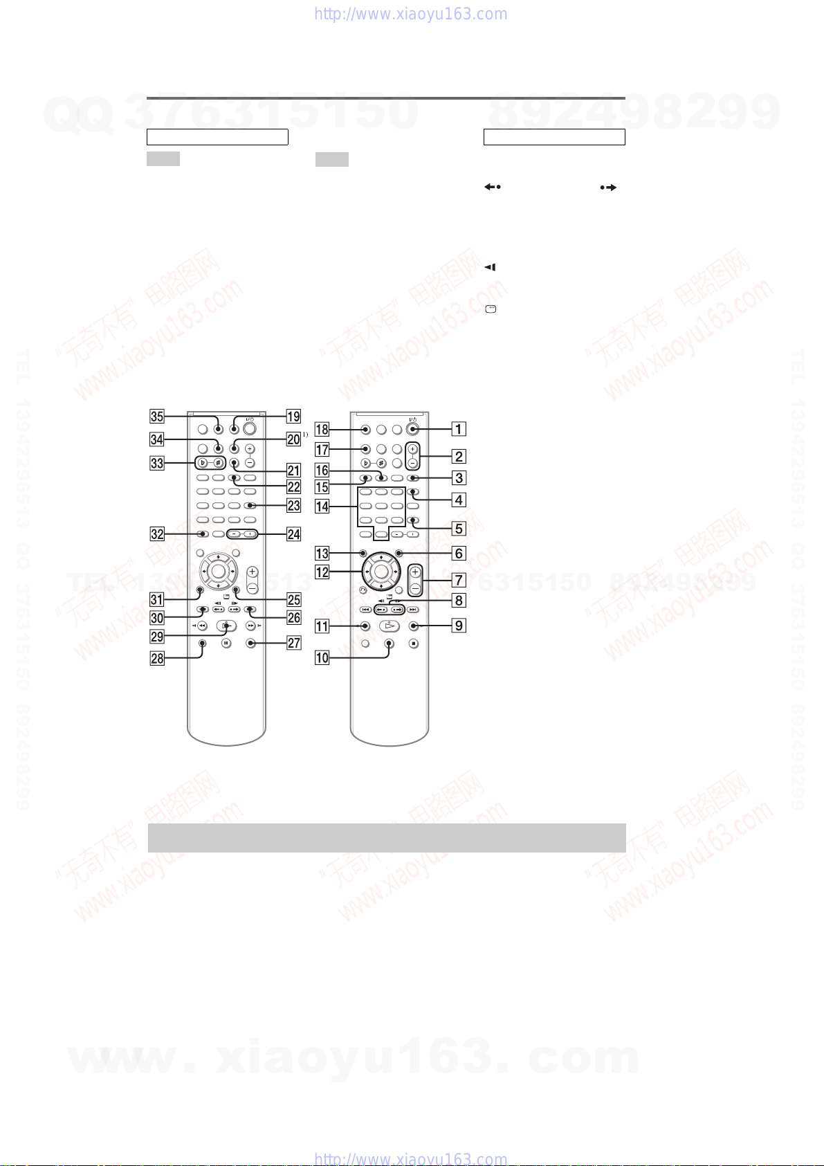
Remote control
7
Q
Q
TEL 13942296513 QQ 376315150 892498299
3
ALBUM +/− wf
ANGLE 5
AUDIO 4
CLEAR es
DISC SKIP
DISPLAY qj
ENTER qs
FM MODE ws
FUNCTION +/− 2
KARAOKE MODE qg
KARAOKE PON qh
MENU 6
Number buttons
PICTURE NAVI 3
PRESET + wh
PRESET − e;
6
ALPHABETICAL ORDER
A – Q
1)
w;
3
2)
qf
1
5
1
R – Z
REPEAT ws
SLEEP qk
SOUND FIELD wa
SUBTITLE wd
THEATRE SYNC ql
TIMER MENU eg
TIME/TEXT ef
TOP MENU qd
TUNING + 9
TUNING − qa
TV wk
TV CH + wh
TV CH − e;
TV/VIDEO qk
TV VOL +/−
VOLUME +/−
5
2)
7
2)
7
0
4
2
9
8
BUTTON DESCRIPTIONS
?/1 (power) 1
TV ?/1 1
REPLAY/ADVANCE
8
c STEP/STEP C 8
SLOW y 9
M (fast forward) 9
X (pause) q;
SLOW qa
m (rewind) qa
M/m/</, qs
DISPLAY wg
> (go forward) wh
x (stop) wj
. (go back) e;
H (play)
O RETURN ea
-/-- es
KEY CONTROL
1)
2)
2)
wl
#/2
ed
The DISC SKIP button is not
available for this model.
The H, number 5 and
VOLUME + (TV VOL +)
buttons have tactile dots. Use
the tactile dots as references
when operating the system.
9
8
2
9
9
TEL 13942296513 QQ 376315150 892498299
TEL
13942296513
Setting the clock
Use buttons on the remote for the operation.
1
Press ?/1 to turn on the system.
2
Press TIMER MENU.
3
Press M or m repeatedly to set the hour.
4
Press ENTER.
5
Press M or m repeatedly to set the
minute.
6
Press ENTER.
The clock starts working.
0
5
1
5
1
3
6
7
3
Q
Q
To adjust the clock
1
Press TIMER MENU.
2
Press M or m to select “CLOCK SET?”, then
press ENTER.
3
Do the same procedures as step 3 to 6
above.
Notes
• The clock settings are canceled when you disconnect
the power cord or if a power failure occurs.
• You cannot set the clock in Power Saving Mode.
8
9
2
4
9
8
2
9
9
10
w
w
w
.
xia
o
y
u
1
6
3
.
c
o
m
Page 11

Q
• This set can be disassembled in the order shown below.
7
Q
3
3-1. DISASSEMBLY FLOW
3-2. SIDE PANEL (A)/(B)
6
SET
(Page 12)
3
1
5
1
SECTION 3
DISASSEMBLY
5
0
8
9
2
4
HCD-AZ2D/AZ5D
2
9
8
9
9
3-3. FRONT PANEL SECTION
(Page 12)
TEL 13942296513 QQ 376315150 892498299
3-5. TOP PANEL (TC) SECTION
(Page 13)
3-6. TAPE MECH DECK
(CMAL5Z230) (DECK-A)
(Page 14)
7
3
Q
Q
3-11. HOLDER (BU) ASSY
(Page 17)
3-12. LEVER (BU LOCK)
(Page 17)
TEL
3-4. TAPE MECH DECK
(CMAL1Z254A) (DECK-B)
(Page 13)
3-9. OPTICAL PICK-UP BLOCK
(KHM-310CAB)
(Page 16)
13942296513
3-10. MOTOR (PULLEY) ASSY
(LOADING) (M001)
(Page 16)
3-7. DC FAN (M901)
(Page 14)
1
5
1
3
6
3-8. DVD MECHANISM DECK
(CDM86-DVBU101)
(Page 15)
4
2
9
8
0
5
9
8
2
9
TEL 13942296513 QQ 376315150 892498299
9
w
w
3-15. CHASSIS (TOP)
(Page 19)
3-16. LEVER (LOADING-L/R)
(Page 20)
w
.
xia
3-13. CLOSE LEVER
(Page 18)
3-14. LEVER (DIR),
GEAR (IDL-B)
(Page 18)
3-17. LEVER (DISC SENSOR)/
(DISC STOP)
(Page 21)
o
y
u
1
6
3
3-18. GEAR (IDL-C)
(Page 21)
.
c
o
m
11
Page 12
HCD-AZ2D/AZ5D
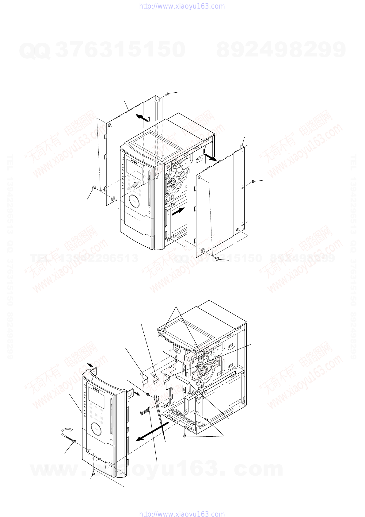
Note: Follow the disassembly procedure in the numerical order given.
7
Q
Q
3-2. SIDE PANEL (A)/(B)
3
6
1
3
5
side panel (A)
5
4
1
5
0
2
three screws
(BVTP 3
×
8)
8
9
4
2
9
side panel (B)
9
8
2
9
9
TEL 13942296513 QQ 376315150 892498299
3
1
three flat head screws
7
TEL
3-3. FRONT PANEL SECTION
13942296513
6
wire (flat type) (11 core)
(CN111)
Q
3
two claws
Q
3
7
6
8
3
0
5
1
5
1
6
three flat head screws
7
three screws
(BVTP 3
9
8
2
×
4
8)
9
8
2
9
TEL 13942296513 QQ 376315150 892498299
9
12
q;
front panel section
9
connector
(CN1050)
w
w
5
wire (flat type) (13 core)
(CN113)
w
1
two screws
(BVTP 3
.
1
screw
(BVTP 3
xia
×
8)
×
8)
4
2
three ground wires
9
connector
y
(CN302)
u
1
6
o
3
8
wire (flat type) (8 core)
(CN304)
1
two screws
(BVTP 3
.
c
7
wire (flat type) (5 core)
(CN112)
×
8)
o
m
Page 13

s
)
Q
3-4. TAPE MECH DECK (CMAL1Z254A) (DECK-B)
Q
3
7
6
3
1
5
6
wire (flat type) (8 core)
1
5
0
3
two screws
(BVTP 2.6)
8
2
9
2
cover (TCM B)
4
1
two screw
(BVTP 2.6
HCD-AZ2D/AZ5D
2
9
8
9
9
5
TEL 13942296513 QQ 376315150 892498299
7
tape mech deck (CMAL1Z254A) (deck-B)
3-5. TOP PANEL (TC) SECTION
3
ground wire
TEL
13942296513
4
top panel (TC) section
Q
Q
3
4
7
3
two screws
(BVTP 2.6)
ground wire
1
3
6
5
1
5
0
2
screw
(BVTP 3
8
2
9
2
two screws
(BVTP 3
×
4
8)
9
×
8)
8
2
9
TEL 13942296513 QQ 376315150 892498299
9
w
w
w
.
xia
2
screw
(BVTP 3
1
connector
(CN301)
o
×
8)
y
u
1
6
3
.
c
o
m
13
Page 14

)
HCD-AZ2D/AZ5D
3-6. TAPE MECH DECK (CMAL5Z230) (DECK-A)
7
Q
Q
TEL 13942296513 QQ 376315150 892498299
3
3
wire (flat type) (7 core)
6
4
two screws
(BVTP 2.6)
3
1
5
1
5
0
6
tape mech deck (CMAL5Z230) (deck-A)
5
ground wire
8
9
2
4
9
8
2
9
9
TEL 13942296513 QQ 376315150 892498299
TEL
3-7. DC FAN (M901)
3
tuner unit (TM-10KR) (AZ2D: Korean model)
tuner unit (TM-10E) (except AZ2D: Korean model)
13942296513
7
connector
(CN954)
4
screw
(BVTT 3
1
wire (flat type) (9 core)
4
two screws
(BVTP 2.6)
2
cover (TCM A)
1
three screws
(BVTP 2.6)
9
9
2
8
9
4
2
9
8
0
5
1
5
1
3
6
7
3
Q
Q
5
screw
×
6)
(BVTP 3
6
×
8) (AZ2D)
2
two screws
(BVTP 3
×
8)
5
seven screws
(BVTP 3
8
two screws
(BVTP 3
5
two screws
(BVTP 3
×
8)
×
8)
×
8) (AZ5D
14
w
w
w
.
xia
9
DC fan (M901)
o
y
u
1
6
3
.
5
screw
(BVTP 3
c
5
screw
(BVTP 3
q;
back panel
×
8)
o
m
×
8)
Page 15

Q
3-8. DVD MECHANISM DECK (CDM86-DVBU101)
Q
3
7
6
CAUTION
9
Be sure to execute a solder bridge as a measure against
static electricity when removing the OP block (DVBU101).
(Otherwise, the OP block will be destroyed.)
3
1
5
1
5
0
8
9
2
4
HCD-AZ2D/AZ5D
2
8
9
8
Lift up the FFC holder.
9
9
TEL 13942296513 QQ 376315150 892498299
7
two claws
2
two claws
TEL
13942296513
Q
6
Q
3
7
6
3
1
5
1
9
8
0
5
q;
wire (flat type) (24 core)
4
wire (flat type) (7 core)
(CN001)
2
4
9
8
2
9
TEL 13942296513 QQ 376315150 892498299
9
w
w
3
1
three screws
(BVTP 3 × 8)
NOTE WHEN REMOVING DVD MECHANISM DECK (CDM86-DVBU101)
Some Screws on the CDM86-DVBU101 are hidden by the Front Panel,
and accordingly remove four Screws (BVTP3x8) on the Front Panel and
shift the Front Panel toward the front, and then remove the Screws on the CDM86-DVBU101.
w
.
xia
o
y
u
1
1
screw
(BVTP 3 × 8)
6
3
.
qa
c
connector
o
5
three screws
(BVTP 3 × 8)
qs
DVD mechanism deck
(CDM86-DVBU101)
m
15
Page 16
s
HCD-AZ2D/AZ5D
3-9. OPTICAL PICK-UP BLOCK (KHM-310CAB)
7
Q
Q
TEL 13942296513 QQ 376315150 892498299
3
6
3
1
3
optical pick-up block
(KHM-310CAB)
2
5
two insulators
1
5
0
8
2
two insulators
9
2
4
9
8
2
9
9
TEL 13942296513 QQ 376315150 892498299
1
two insulator screws
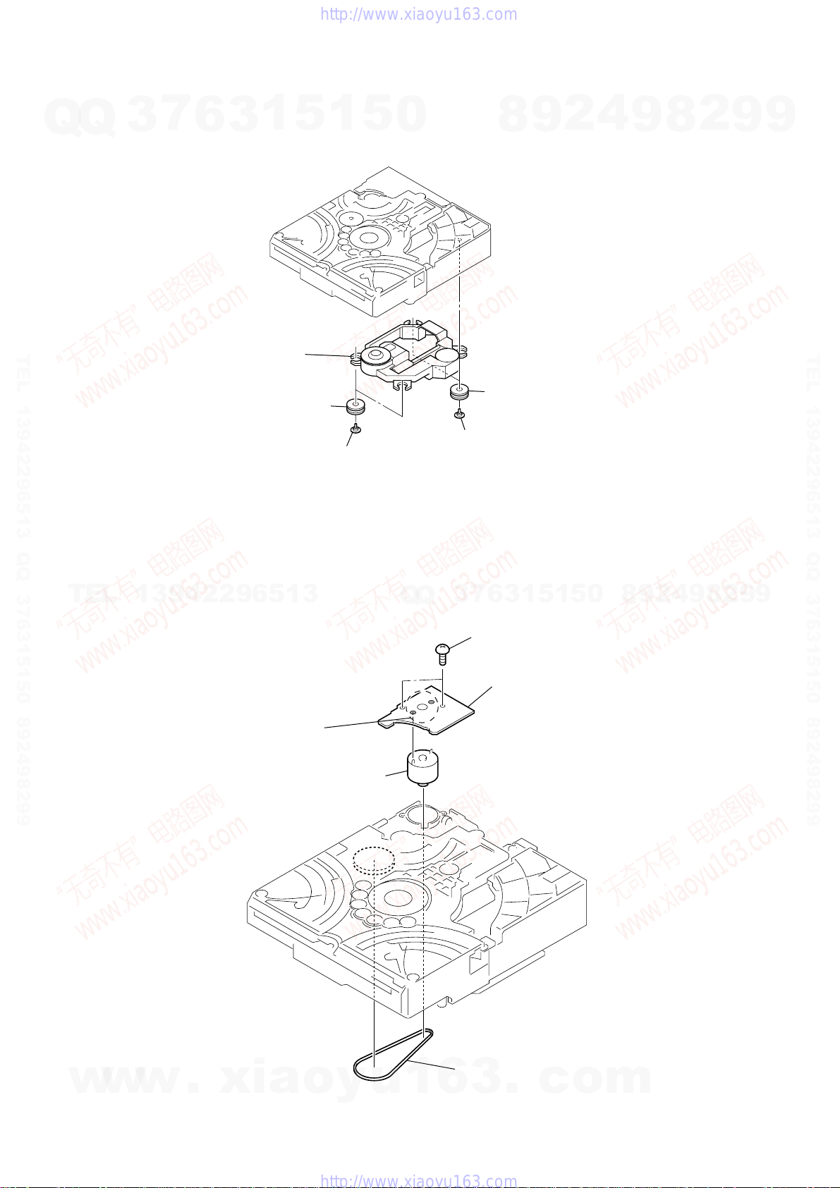
3-10. MOTOR (PULLEY) ASSY (LOADING) (M001)
TEL
13942296513
3
Remove two solders.
4
motor (pully) assy (loading)
(M001)
Q
Q
1
two insulator screw
3
6
7
3
2
two screws
(B 2.6 × 8)
5
MS-214 board
1
5
1
5
0
8
9
2
4
9
8
2
9
9
16
w
w
w
.
xia
1
o
y
u
1
6
3
belt (MOT)
.
c
o
m
Page 17
)
Q
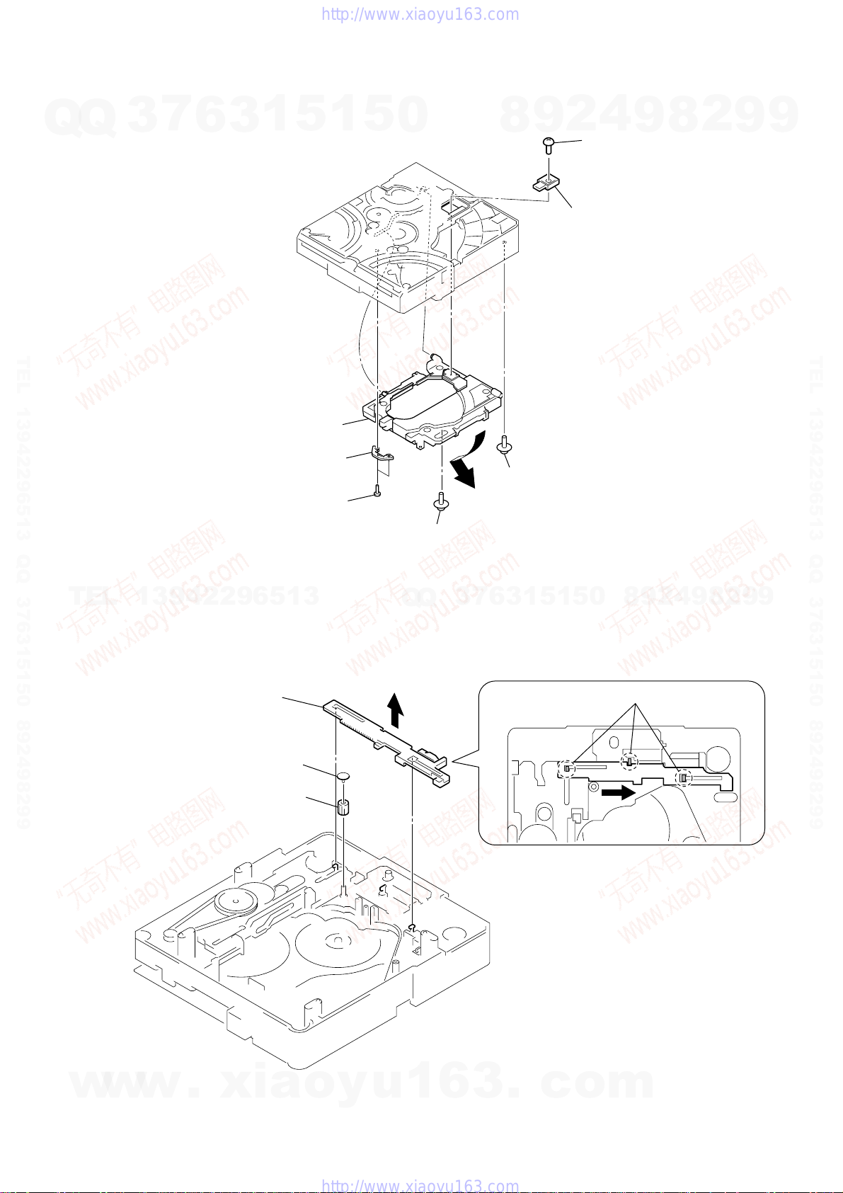
3-11. HOLDER (BU) ASSY
7
Q
3
6
3
1
5
1
5
0
8
9
2
1
2
lever (CL UP2
4
screw
(B 2.6
HCD-AZ2D/AZ5D
2
9
×
8)
8
9
9
TEL 13942296513 QQ 376315150 892498299
6
holder (BU) assy
4
LHL support
3
two screws
(B 2
×
6)
5
floating screw
(PTPWH M2.6)
TEL
13942296513
3-12. LEVER (BU LOCK)
4
lever (BU lock)
Q
Q
3
7
6
5
3
floating screw
(PTPWH M2.6)
5
1
5
1
0
3
2
9
8
three hooks
4
9
8
2
9
TEL 13942296513 QQ 376315150 892498299
9
w
w
w
2
.
xia
1
gear (cap)
gear (BU lock)
o
y
u
1
6
3
.
c
o
m
17
Page 18

HCD-AZ2D/AZ5D
3-13. CLOSE LEVER
7
Q
Q
3
6
3
1
5
1
5
0
5
close lever
3
claw
9
8
1
washer (3-1-0.4)
2
SPR-E lever close
4
shaft disc stop
2
4
9
8
2
9
9
TEL 13942296513 QQ 376315150 892498299
TEL
3-14. LEVER (DIR), GEAR (IDL-B)
13942296513
2
claw
washer
Q
3
nylon washer 1.7
Q
4
7
3
pulley (gear)
5
gear (cap)
6
gear (IDL-A)
6
3
1
5
1
5
0
8
9
9
stoper
2
4
9
8
2
9
TEL 13942296513 QQ 376315150 892498299
9
18
7
Loosen the screw.
8
w
Hold the release lever
w
w
and change the direction.
1
tension coil spring (DIR)
.
xia
0
Lever (DIR)
o
y
u
1
6
3
qa
gear (IDL-B)
.
c
o
m
Page 19

)
3-15. CHASSIS (TOP)
7
Q
Q
TEL 13942296513 QQ 376315150 892498299
3
6
3
5
chassis (top)
1
3
two screws
(B 2 × 10)
5
4
three screws
(B 2.6 × 8)
1
5
0
8
9
2
4
1
2
HCD-AZ2D/AZ5D
2
8
9
screw
(B 2.6 × 8)
lever (CL UP2
9
9
TEL 13942296513 QQ 376315150 892498299
TEL
13942296513
Q
Q
3
7
6
3
1
5
1
5
0
8
9
2
4
9
8
2
9
9
w
w
w
.
xia
o
y
u
1
6
3
.
c
o
m
19
Page 20
HCD-AZ2D/AZ5D
)
3-16. LEVER (LOADING-L/R)
7
Q
Q
3
6
3
1
5
1
5
0
8
9
2
4
9
8
2
9
9
1
SPT-T (loading-R) SPR-T (loading-L)
TEL 13942296513 QQ 376315150 892498299
5
lever (loading-R)
TEL
13942296513
4
two hooks
Q
Q
1
3
7
6
3
2
two hooks
5
1
0
5
1
3
lever (loading-L
8
9
2
4
9
8
2
9
TEL 13942296513 QQ 376315150 892498299
9
20
w
w
w
.
xia
PRECAUTION DURING LEVER (LOADING R / L) INSTALLATION
.
c
lever (loading-L)
Install the
both levers so that they move symmetrically.
o
BOTTOM VIEW
Align the horizontal position.
y
u
1
6
lever (loading-R)
3
o
m
Page 21

Q
3-17. LEVER (DISC SENSOR)/(DISC STOP)
Q
3
7
6
3
1
5
1
5
1
gear (cap)
2
0
gear (IDL L)
HCD-AZ2D/AZ5D
4
2
9
8
PRECAUTION DURING DISC STOP LEVER INSTALLATION
9
8
2
9
9
TEL 13942296513 QQ 376315150 892498299
5
two hooks
3
two claws
6
lever (disc stop)
4
lever (disc sensor)
TEL
13942296513
3-18. GEAR (IDL-C)
3
gear (IDL-D)
2
two claws
Q
Q
4
three hooks
3
7
hole
hole
Install the lever (disc stop) so that the both holes
are aligned.
8
0
5
1
5
1
3
6
chassis (top)
lever (disc stop)
4
2
9
9
8
2
9
TEL 13942296513 QQ 376315150 892498299
9
w
w
w
1
gear (IDL-F)
.
xia
7
gear (IDL-C)
6
claw
o
y
u
1
6
3
5
lever (gear loading) assy
.
c
o
m
21
Page 22
HCD-AZ2D/AZ5D
SECTION 4
TEST MODE
COLD RESET
The cold reset clears data except DVD data stored in the RAM to
Q
Q
initial conditions. Execute this mode when returning the set to the
customers.
Procedure:
1. Press the
2. Press two buttons of
simultaneously.
3. The message “COLD RESET” is displayed on the fluorescent
indicator tube, then become standby mode.
PANEL TEST MODE
This mode is used to check the fluorescent indicator tube, LED,
model, destination, software version and key.
Procedure:
1. Press two buttons of [DIMMER] , [DIRECTION] and touch the
TEL 13942296513 QQ 376315150 892498299
MEMORY CLEAR MODE
This mode moves clears main microprocessor data stored in the
RAM to initial conditions. Use this mode when returning the set to
the customer after repair.
Procedure:
sensor simultaneously.
x
2. All LEDs and segments in fluorescent indicator tube are lighted
up.
3. When you want to enter the software version display mode,
touch the
4. Each time
destination, MC version, SYS version, UI version, DVD
version, ST version, TA version, TM version, TC version in
this order, and returns to the model name display.
5. When
6. Press the [DSGX] button, the key check mode is activated.
7. In the key check mode, the fluorescent indicator tube displays
8. To release from this mode, press three buttons in the same
1. Press the
2. Touch the [DVD] sensor to select the “DVD”.
3. Press the [EQ SELECT] button and touch two sensors of [DVD],
4. After the “STANDBY” blinking display finish, the message
>
being displayed except model name and destination, the date
of the software creation appear. When
again, the display returns to the software version display. When
–
.
sensor is touched while the date of the software creation
is being displayed, the date of the software creation is displayed
TEL
in the same order of software version display.
“K 0”. Each time a button is pressed, “K 0” value increases.
However, once a button has been pressed, it is no longer taken
into account.
manner as step 1 or disconnect the power cord.
simultaneously.
x
“MECH A LOCK” is displayed on the fluorescent indicator
tube.
7
3
button to turn the power on.
?/1
–
.
–
.
+
sensor is touched while the version numbers are
6
, [DISPLAY]and touch the
?/1
sensor. The model name is displayed.
sensor is touched, the display changes from
3
1
5
+
sensor is touched
>
1
x
13942296513
button to turn the power on.
?/1
5
sensor
DISC SLOT LOCK
This mode let you lock the disc slot. When this mode is activated,
0
the disc will not eject when
“LOCKED” will be displayed in on the fluorescent indicator tube.
Procedure:
1. Press the
2. Touch the [DVD] sensor to select the “DVD”.
3. Touch the
and hold down until “LOCKED” or “UNLOCKED” displayed
on the fluorescent indicator tube (around 5 seconds).
TUNER STEP CHANGE
(Except Saudi Arabian and Russian models)
The step interval of AM channels can be toggled between 9 kHz
and 10 kHz.
Procedure:
1. Press the
2. Touch the [TUNER/BAND] sensor to select the “AM”.
3. Press the
4. Touch the
The set power on automatically. The message “AM 9k Step”
or AM10k Step” displayed on the fluorescent indicator tube
and thus the channel step is changed.
FUNCTION NAME CHANGE
This mode let you change from VIDEO to SAT and vice-versa.
Procedure:
1. Press the
2. Touch the [VIDEO/SAT] sensor and press
simultaneously. The set power on automatically and the
function will changed to SAT. Do the same procedures again
7
3
to change from SAT to VIDEO.
Q
Q
COLOR SYSTEM CHANGE
(Except Latin American and Russian models)
This mode let you change the color system of the video output from
PAL to NTSC or vice-versa.
Procedure:
1. Press the
2. Touch the [DVD] sensor to select the “DVD”.
3. Press the
4. Touch the
5. The message “COLOR PAL” or “COLOR NTSC” will be
displayed on the fluorescent indicator tube.
4
8
button to turn the power on.
?/1
x
sensor and press the Z button simultaneously
button to turn the power on.
?/1
button to turn the power off.
?/1
–
.
sensor and press
button to turn the power on.
?/1
1
3
6
button to turn the power on.
?/1
button to turn the power off.
?/1
sensor and press
X
button is pressed. The message
Z
?/1
8
0
5
1
5
button simultaneously.
?/1
2
9
8
9
button simultaneously.
?/1
9
4
2
9
2
button
2
8
9
9
9
TEL 13942296513 QQ 376315150 892498299
9
22
w
w
w
.
xia
o
y
u
1
6
3
.
c
o
m
Page 23

HCD-AZ2D/AZ5D
DVD SECTION
7
Q
Q
TEL 13942296513 QQ 376315150 892498299
TEL
3
1. DVD SERVICE MODE GENERAL DESCRIPTION
The Mirror Time and TOP measurement allows you to make
diagnosis and adjustment simply by using the remote commander
and monitor TV. The instructions, diagnosis results, etc. are given
on the on-screen display (OSD).
2. STARTING DVD SERVICE MODE
1. Press the
2. Touch the [DVD] sensor to select the “DVD”.
3. Press the Z button and touch two sensors of x , [VOLUME
+] simultaneously.
4. The message “SERVICE IN” will be displayed on the
fluorescent indicator tube and the Rimocon Diagnosis Menu
is displayed on the on-screen display on the monitor TV as
follows. The model name, IF-con version and Syscon version
is displayed at the bottom of the on-screen display.
0. External Chip Check
1. Servo Parameter Check
2. Drive Manual Operation
3. Emergency History
4. Version Information
5. Video Level Adjustment
Model Name :AZXD_XX
IF-con :Ver.xx.xx (xxxx)
Syscon :Ver.x.xxx
13942296513
5. To execute each function, press its number by using numeric
button on the remote commander (RM-AMU001)
6. To release from this mode, press the
power off.
6
button to turn the power on.
?/1
Remocon Diagnosis Menu
3
1
5
1
5
button to turn the
?/1
0
Q
Q
4. MIRROR TIME ADJUSTMENT
On the Drive Manual Operation menu screen, press [5] button on
the remote commander, and the following MIRR time Adjust Menu
will be displayed.
There are five main commands in the Mirr time Adjust menu. The
functions of each command are described in the following page.
1. CD MIRR time Check
This command checks the Mirror time value for CD disc.
2. DVD MIRR time Check
This command checks the Mirror time value for DVD disc.
3. Threshold
This command displays the threshold value between CD and DVD
mirror time.
4. Save to EEPROM
7
3
This command saves an adjusted mirror time value to the EEPROM.
5. Default set MIRR time
This command will set CD and DVD mirror time to firm ware default
value.
4
2
9
8
MIRR time Adjust Menu
1. CD MIRR time Check:
2. DVD MIRR time Check:
3. Threshold:
4. Save to EEPROM
5. Default set MIRR time
[Open] Tray open [Close] tray close
[0] Return to previous menu
0
5
1
5
1
3
6
9
8
9
2
8
4
2
9
8
2
9
9
9
TEL 13942296513 QQ 376315150 892498299
9
3. DRIVE MANUAL OPERATION
The Drive Manual Operation menu consists of five main functions.
On the Remocon Diagnosis Menu screen, press [2] button on the
remote commander, and the following Drive Manual Operation
menu will be displayed.
Drive Manual Operation
1. Servo Control
2. Track/Layer Jump
3. Manual Adjustment
4. Tray Aging Mode
5. MIRR time Adjust
0. Return to Top Menu
w
w
w
.
xia
o
y
u
1
[Open]/[Close]
Pressing the
time adjustment.
[0] Return to previous menu.
Press the [0] button on the remote commander to return to previous
menu.
EXECUTING MIRROR TIME ADJUSTMENT
In order to execute mirror time adjustment, the following standard
procedures must be followed.
1. Set to the MIRR time Adjust Menu mode.
2. Press the [5] button on the remote commander to select the “5
3. Press the [3] button on the remote commander to select the “3
4. Check the value of Threshold on the screen. If it is 75, go to
6
3
Z
button controls the tray for disc change during mirror
Default set MIRR time”.
Threshold”.
next step. If it is not so, return to step 2.
.
c
o
m
23
Page 24

HCD-AZ2D/AZ5D
17. Take out the CD test disc (YEDS-18)
MIRR time Adjust Menu
7
Q
Q
1. CD MIRR time Check:
2. DVD MIRR time Check:
3. Threshold: 75
4. Save to EEPROM
5. Default set MIRR time
[Open] Tray open [Close] Tray close
[0] Return to previous menu
5. Insert the DVD test disc (HLX-504) (Part No.J-6090-088-A)
6. Press the [2] button on the remote commander to select the “2
TEL 13942296513 QQ 376315150 892498299
DVD MIRR time Check”.
7. Wait for hexadecimal value to display on the screen.
8. Check the value (##) of DVD MIRR time on the screen. If ##
is 28 to 70, go to next step. If it is not so, return to step 5.
MIRR time Adjust Menu
1. CD MIRR time Check:
2. DVD MIRR time Check: $$ ##
3. Threshold:
4. Save to EEPROM
5. Default set MIRR time
3
6
3
1
5
1
5
18. Release the MIRR time Adjust Menu mode.
0
5. EXECUTING IOP MEASUREMENT
In order to execute IOP measurement, the following standard
procedures must be followed.
1. Set to the Drive Manual Operation mode.
2. Press the [3] button on the remote commander, and the
following Manual Adjust menu will be displayed.
1. Track Balance Adjust:
2. Track Gain Adjust:
3. Focus Balance Adjust:
4. Focus Gain Adjust:
5. Eq Boost Adjust:
6. Iop:
7. TRV. Level:
8. S curve (FE) Level:
9. RFL(PI) Level:
0. MIRR Time:
Change Value
↑↓
[RETURN] Return to previous menu
3. Press the [6] button on the remote commander to select the
“6. IOP”.
4. Wait for hexadecimal Value to display on the screen.
9
8
Manual Adjust
2
4
9
8
2
9
9
TEL 13942296513 QQ 376315150 892498299
TEL
[Open] Tray open [Close] Tray close
[0] Return to previous menu
9. Press the [4] button on the remote commander to select the “4.
Save to EEPROM”
10. Check that $$ is the same as the value of ## on the screen. If
it is not so, return to step 5.
11. Take out the DVD test disc (HLX-504) and insert the CD test
disc (YEDS-18) (Part No.3-703-998-01).
12. Press the [1] button on the remote commander to select the
“1.CD MIRR time Check”.
13. Wait for hexadecimal value to display on the screen.
14. Check the value (@@) of CD MIRR time on the screen. If @@
is 5A to E8, go to next step. If it is not so, return to step 11.
1. CD MIRR time Check: && @@
2. DVD MIRR time Check: $$ ##
3. Threshold:
4. Save to EEPROM
5. Default set MIRR time
[Open] Tray open [Close] Tray close
[0] Return to previous menu
15. Press the [4] button on the remote commander to select the “4.
Save to EEPROM”.
16. Check that && is the same as the value of @@ on the screen. If
w
it is not so, return to step 11.
13942296513
MIRR time Adjust Menu
w
w
.
xia
o
y
Manual Adjust
1. Track Balance Adjust:
Q
u
3. Focus Balance Adjust:
4. Focus Gain Adjust:
5. Eq Boost Adjust:
6. Iop: ED
7. TRV. Level:
8. S curve(FE) Level:
9. RFL(PI) Level:
0. MIRR Time:
[RETURN] Return to previous menu
5. Convert value (ED) from hexadecimal to decimal using
conversion table.
6. If the remainder is smaller than 93 (decimal), then it is OK.
However if the value is higher than 93, then the BU (base
unit) is defective and need to be change.
7. Release the Manual Adjust menu mode.
6. DVD RAM CLEAR
This mode clears DVD data stored in the DVD RAM to initial
conditions.
1. On the Rimocon Diagnosis Menu screen, press [4] button on
the remote commander to select the “4.Version Information”.
2. Press in order of [MENU] button and [CLEAR] button on the
remote commander.
3. Press in order of [MENU] button and [CLEAR] button on the
remote commander to clear DVD data.
4. The message “Initialize all data” will be displayed on the
screen.
5. The message will change into “Initialize all data Complete”
in about six seconds, and the clearness of the DVD data is
1
6
completed.
2. Track Gain Adjust:
Q
6
7
3
Change Value
↑↓
3
3
.
1
5
c
1
0
5
o
m
8
9
2
4
9
8
2
9
9
24
Page 25

set
MAIN board
VIDEO/SAT OUT
jack (J101)
+
–
level meter
test tape
P-4-A063
(6.3 kHz, –10 dB)
SECTION 5
MECHANICAL ADJUSTMENTS
HCD-AZ2D/AZ5D
SECTION 6
ELECTRICAL ADJUSTMENTS
PRECAUTION
Q
TEL 13942296513 QQ 376315150 892498299
1. Clean the following parts with a denatured-alcohol-moistened
Q
2. Demagnetize the record/playback head with a head
3. Do not use a magnetized screwdriver for the adjustments.
4. After the adjustments, appiy suitable locking compound to
5. The adjustments should be performed with the rated power
• Torque Measurement
FWD CQ-102C 31 to 71 g⋅cm
FWD
Back Tension
REV CQ-102RC 31 to 71 g⋅cm
REV
Back Tension
FF/REW CQ-201B 71 to 143 g⋅cm
TEL
FWD Tension CQ-403A 100 g or more
REV Tension CQ-403R 100 g or more
7
3
swab :
record/playback head pinch roller
erase head rubber belts
capstan idlers
demagnetizer.
the parts adjusted.
supply voltage unless otherwise noted.
Mode Torque Meter Meter Reading
6
13942296513
1
5
1
3
3.06 N⋅m to 6.96 N⋅m
(0.43 – 0.98 oz⋅inch)
0.19 N⋅m to 0.58 N⋅m
CQ-102C 2 to 6 g⋅cm
(0.02 – 0.08 oz⋅inch)
3.06 N⋅m to 6.96 N⋅m
(0.43 – 0.98 oz⋅inch)
0.19 N⋅m to 0.58 N⋅m
CQ-102RC 2 to 6 g⋅cm
(0.02 – 0.08 oz⋅inch)
6.96 N⋅m to14.02 N⋅m
(0.98 – 1.99 oz⋅inch)
5
9.80 N⋅m
(3.53 oz or more)
9.80 N⋅m
(3.53 oz or more)
0
Q
Q
DECK SECTION
1. Demagnetize the record/playback head with a head
2. Do not use a magnetized screwdriver for the adjustments.
3. After the adjustments, apply suitable locking compound to the
TEST Tape
RECORD/PLAYBACK HEAD AZIMUTH ADJUSTMENT
DECK–A DECK–B
Note: Perform this adjustments for both decks.
Procedure:
1. Mode: Playback
2. Turn the adjustment screw and check output peaks. If the peaks
7
3
0 dB=0.775 V
4
2
9
8
demagnetizer.
parts adjust.
Tape Signal Used for
P-4-A063 6.3 kHz, -10 dB Azimuth Adjustment
do not match for L-CH and R-CH, turn the adjustment screw
so that outputs match within 1dB of peak.
6
3
L-CH
peak
1
5
1
0
5
Output
level
8
within
1dB
9
9
2
8
4
2
9
8
9
2
9
within
1dB
9
9
TEL 13942296513 QQ 376315150 892498299
w
w
w
.
xia
o
y
u
1
6
3
Screw
position
.
R-CH
peak
c
o
L-CH
peak
m
R-CH
peak
Screw
position
25
Page 26

HCD-AZ2D/AZ5D
e
V
3. Mode: Playback
7
Q
Q
test tape
P-4-A063
(6.3 kHz, –10 dB)
TEL 13942296513 QQ 376315150 892498299
4. After the adjustments, apply suitable locking compound to
the pats adjusted.
Adjustment Location: Playback Head (DECK-A)
3
in phase 45°90°135°180
6
MAIN board
VIDEO/SAT OUT
jack (J101)
set
waveform of oscilloscope
good
Record/Playback/Erase Head (DECK-B)
3
1
5
oscilloscope
V
wrong
1
5
H
°
DVD SECTION
0
RFMON LEVEL CHECK
DMB10 board
CN105 pin
CN105 pin
Procedure :
1. Connect the oscilloscope to CN105 pin 6 (RFMON) and
CN105 pin 3 (GND) on the DMB10 board.
2. Press the `/1 button to turn the power on.
3. Insert the test disc (DVD: TDV-520CSO (Part No. J-2501236-A), CD: LUV-P01 (Part No. 4-999-032-01) and touch the
Y sensor to playback.
4. Confirm that oscilloscope waveform is as shown in the
figure below. (eye pattern)
A good eye pattern means that the diamond shape (◊) in the
center of the waveform can be clearly distinguished.
8
6
(RFMON)
3
9
(GND)
2
4
9
oscilloscop
(DC range)
+
–
2
8
VOLT/DIV: 200 m
TIME/DIV: 500 ns
9
9
TEL 13942296513 QQ 376315150 892498299
TEL
reverse
forward
13942296513
forward
1
3
6
7
3
Q
Q
Checking Location:
– DMB10 BOARD (Side A) –
5
5
1
IC102
level:
0.8
0.8 ± 0.2 Vp-p (CD)
8
0
±
0.2 Vp-p (DVD)
9
4
2
9
CN105
1
IC201
6
8
2
9
9
26
w
w
w
.
xia
o
y
u
1
6
3
.
c
o
m
Page 27

SECTION 7
DIAGRAMS
7-1. BLOCK DIAGRAM – RF SERVO/VIDEO SECTION –
Q
TEL 13942296513 QQ 376315150 892498299
Q
OPTICAL PICK-UP
BLOCK
(KHM-310CAB)
VR (780)
T
E
(LOADING)
w
RF
VOA/A
VOB/B
VOC/C
VOD/D
PD
MSW
L
FCS+
FCS– 37
TRK+ 35
TRK– 34
SL+ 29
SL– 30
SP+ 27
SP– 28
M001
REGO2
REGO1
w
3
AUTOMATIC POWER
CONTROL (FOR CD)
AUTOMATIC POWER
CONTROL (FOR DVD)
CD ON
SWITCH
Q101-1
DVD ON
SWITCH
Q101-2
1
FOCUS/TRACKING COIL DRIVE,
SPINDLE/SLED/LOADING MOTOR DRIVE
36
46
47
M
25
24
42
31
32
w
7
Q102-1
Q102-2
Q103
3
IC201
FOCUS
COIL DRIVE
TRACKING
COIL DRIVE
SLED
MOTOR DRIVE
SPINDLE
MOTOR DRIVE
BUFFER
LOADING
MOTOR DRIVE
BUFFER
REGULATOR
9
MUTE5 21
4
1
4
10
13
45
16
17
15
19
22
40
8
.
6
2
3
ASDATA0 217 LOUT1+ 2
DVDRF IP
6
8
MA
9
MB
10
MC
11
MD
ASDATA1 218 LOUT2+ 46
DVDA2
DVDB3
DVDC4
DVDD5
TNI18VOE/E+G
ASDATA2 219 LOUT3+ 42
TPI19VOF/F+H
V2029VC
MDI120
MDI221
ASDATA4 222 LOUT4+ 38
LDO123LD (780)
LDO2
22LD (650)
RF AMP, SERVO DSP,
MPEG DECODER
IC102
SPDATA 209
MSW
187VR (650)
(AZ5D)
2
176LIMIT
LIMSW
(AZ2D)
FOO42
TRO41
FMO38
DMO37
SPFG47
FWD
186
REV
185
39
TROPENPWM
184
MUTE123MUTE12
MUTEMUTE34 18320
TSDMTSD-M 181
IOPMON40
RF+3.3V
x
9
SPDIF 225
YUV2
YUV1
YUV3
YUV4
YUV5
YUV6
1
6
196
194
198
202
202
203
i
5
ACLK
EEPROM
IC103
1
DQ0 – DQ15
RD0 – RD15
XTALO
228
ABCK
3
o
S003
(TRIGGER)
6
5
SCL
SDA
5
2, 4, 5, 7, 8, 10, 11, 13, 42,
44, 45, 47, 48, 50, 51, 53
125 – 123, 121, 120, 118, 117,
115, 135, 133 – 128, 126
XTALI
229
X101
27MHz
a
ALRCK
104
1
SDTI114
SDTI215 SL
SDTI316 FC
SDTI413 LT
10ACLK 215
MCLK
9ABCK 214
BICK
17ALRCK 213
LRCK
PDN
8XRST 220
SDA
20SDA 103
SCL
19SCL 102
TRG-SW
y
S002
(CHUCKING)
5
LOUT1– 1
48
ROUT1+
47
ROUT1–
D/A CONVERTER
IC301
LOUT2– 45
44
ROUT2+
43ROUT2–
LOUT3– 41
40
ROUT3+
39ROUT3–
(AZ5D)
LOUT4– 37
33
ROUT4+
32ROUT4–
SPDATA
DIGITAL OPTICAL
TRANSCEIVER
IC231
SD-RAM
IC104
A0 – A11
23 – 26,
29 – 34, 22, 35
147, 149 – 151, 166 – 164,
162, 160, 159, 146, 158
RA0 – RA11
CKSW
179
u
S001
(DISC IN/OUT)
0
DVD
DIGITAL
OUT
177
SWITCH
Q2001
20
143
OCKSW
Q
21
145
BA0 BA0
BA1 BA1
1
Q
38
37
156
157
CKE CKE
RCLK CLK
P_DVD_I_MTK
19
_SLOT_IN
CONTROLLER
IC401 (1/5)
MIX AMP
IC3711
MIX AMP
IC3731
MIX AMP
IC3751
MIX AMP
IC3771
15
39
113
137
DQM0 LDQM
6
SYSTEM
18
140
DQM1 UDQM
17
139
RAS /RAS
19
142
CAS /CAS
101
31
3
RCS /CS
P_O_DVD_SO IFSDI
16
138
RWE /WE
98
32
P_I_DVD_SI IFSDO
CENTER VOLTAGE
GENERATOR
VIDEO AMP, 75Ω DRIVER
4
CVBS IN
7
2
C IN
6
Y IN
10
CY IN
12
CB IN
14
CR IN
100
99
105
26
33
28
3
PI_DVD_SCK IFCK
P_I_DVD_XIFCS IXFCS
P_O_DVD_BUSY IFBSY
FL
FR
SR
SW
RT
Q3801
6
114
25
P_I_MREQ MREQ
25S19
171
207
27
IC1201
I/P
188
DSEL
WIDE
110
34
P_I_KRMOD KRMOD
.
8
CVBS OUT
3
S-DC OUT
CY OUT
CB OUT
CR OUT
MUTE113MUTE2
3
23
P_VIDEO_MUTE
P_ID_IO_SYSRST PRST
1
C OUT
Y OUT
9
SW+5V
23
5
26
27
21
20
18
16
c
1
DQ0 – DQ7
29, 31, 33, 35,
38, 40, 42, 44
81 – 84,
86 – 88, 91
AD0 – AD7
o
2
0
5
FLASH ROM
IC101
A-1, A0 – A20
45, 25 – 18, 8 – 1,
48, 17, 16, 9, 10
93, 78, 53 – 59, 75, 74,
72 – 67, 92, 60, 61, 76, 89
IOA0 – IOA21
m
4
CY
9
• SIGNAL PATH
: CD PLAY
: DVD PLAY
: DIGITAL OUT
: AUDIO
: VIDEO
: Y
: CHROMA
: COMPONENT VIDEO
9
8
Y
PB/C
PR/C
26
28
77
79
IOCS CE
B
R
11
66
IOOE OE
8
FL, FR, SL, SR, FC, SW, LT, RT
SPDATA, ACLK, ABCK, ALRCK
(AZ5D)
J1202
VIDEO OUT
4
2
J1201
S VIDEO OUT
J1203
COMPONENT
VIDEO OUT
IOWR WE
MIC 205
9
SWITCH
Q464
2
8
HCD-AZ2D/AZ5D
9
A
(Page 29)
B
(Page 29)
9
2
MIC
C
(Page 29)
9
9
TEL 13942296513 QQ 376315150 892498299
HCD-AZ2D/AZ5D
2727
Page 28
HCD-AZ2D/AZ5D
Q
Q
3
7-2. BLOCK DIAGRAM – TUNER/TAPE SECTION –
7
6
3
1
5
1
5
0
DECK A/B SELECT SWITCH,
FM 75Ω
COAXIAL
AM
REC/PB EQ AMP
IC101 (1/2)
ANTENNA
FM ANT
AM ANT
8
TUNER UNIT
ST-L
ST-R
STDOUT
STDIN
STCLK
STCE
TUNED
9
R-CH
2
4
9
40
38
39
41
37
ST-DIN
ST-DOUT
ST-CLK
ST-CE
ST TUNED
8
2
9
ST-L
D
(Page 29)
9
L-CH
HP301
(PB)
TEL 13942296513 QQ 376315150 892498299
T
E
L
1
3
(DECK-A)
HRPE301
(REC/PB/ERASE)
(DECK-B)
9
4
9
R-CH
R-CH
6
R-CH
L-CH
R-CH
2
2
ERASE
• R-ch is omitted due to same as L-ch.
• SIGNAL PATH
: TUNER (FM/AM)
: TAPE PLAY (DECK-A)
: TAPE PLAY (DECK-B)
: REC
MUTING
MUTING
Q301, 302
BIAS OSC
5
Q303
T301
1
R-CH
R-CH
3
BIAS OSC
Q318
MUTING CONTROL
SWITCH
Q314, 315
MUTING CONTROL
SWITCH
Q311 – 313
REC BIAS
SWITCH
Q316, 317
A+9V
C306, L301
BIAS
TRAP
MUTING
Q104
71
70
AMS
48 50
R-CH
Q
EQ
MUTING CONTROL
SWITCH
Q361
Q
3
9
PB-L
(Page 29)
REC-L
(Page 29)
9
E
TEL 13942296513 QQ 376315150 892498299
F
68
11
10
9
8
7
6
67 66
AMS DETECT
Q341 – 343
AMS MUTING
Q140, 363
1
3
TAPE MECHANISM
DECK BLOCK
A PLAY
B PLAY
A SHUT
B SHUT
A HALF
B HALF
F-REC
R-REC
A TRGM+
(DECK-A)
B TRGM+
(DECK-B)
A CAPM+
M
CAPSTAN/REEL
(DECK-A)
B CAPM+
M
CAPSTAN/REEL
(DECK-B)
5
MUTING
Q103
1
R-CH
MUTING CONTROL
SWITCH
Q362
0
5
TRIGGER PLUNGER
DRIVE (DECK-A)
Q323, 324
TRIGGER PLUNGER
DRIVE (DECK-B)
Q321, 322
CAPSTAN/REEL
MOTOR DRIVE (DECK-A)
Q326, 327
CAPSTAN/REEL
MOTOR DRIVE (DECK-B)
Q328, 329
8
TC LINE MUTE
70
TC AMS IN
75
P_TC_AMS_MUTE
44
TC PB/REC
68
TC REC MUTE
69
SYSTEM CONTROLLER
IC401 (2/5)
2
9
TC BIAS
67
TC A PLAY SW
22
TC B PLAY SW
80
TAPE A SHUT
97
TAPE B SHUT
90
TC A HALF
21
TAPE B HALF/REC
91
TC A TRG
36
TC B TRG
79
TC A CAPM
35
TC B CAPM
78
4
9
8
2
w
HCD-AZ2D/AZ5D
w
w
.
x
i
a
o
y
u
1
6
2828
3
.
c
o
m
Page 29
HCD-AZ2D/AZ5D
7-3. BLOCK DIAGRAM – AUDIO SECTION –
7
USB CONTROL
SWITCH
Q11, 12
DIGITAL ECHO
IC1061
MIC AMP
IC1060 (1/2)
3
9
R-CH
MUTING
Q272
6
9
D+
8 D–
HOST
21
D1
RV1061
ECHO LEVEL
RV1060
MIC LEVEL
4
2
R-CH
MUTING
Q273
3
USB D/A
CONVERTER
IC1
XTI
SSPND1XTO
28
27
X11
12MHz
2
VOUTL
VOUTR
IC1060 (2/2)
9
MIC AMP
VBUS
MUTING
Q270
D+
D–
R-CH
3
3
2
1
CN1
PC
1
MUTING
Q271
Q
TEL 13942296513 QQ 376315150 892498299
(Page 28)
(Page 28)
(Page 27)
VIDEO/SAT
ST-L
D
PB-L
E
J1060
MIC 1
J1061
MIC 2
T
FL, FR, SL, SR,
FC, SW, LT, RT
A
Q
IN
E
J101 (1/2)
L
R
L
LT
RT
FL
FR
SL
SR
SW
1
14
R-CH
15
6
5
MUTING
Q1
MUTING CONTROL
SWITCH
Q113
5
1
AUDIO
+4.5V
3
1
62
63 42 41 37
65
64
74
R-CH
5
6
+
SELECTOR
R-CH
59 56 53
33
A+9V
AUDIO SELECT SWITCH
IC261
X0
12
X1
13
2
1
5
3
X-X1
Y0
Y1
Y-Y1
Z0
Z1
Z-Z1
R-CH
R-CH
X
Y
Z
14
11
15
10
4
9
0
52 51
TONE
+
1
2
R-CH
(AZ5D)
INPUT SELECT SWITCH,TONE CONTROL,
ELECTRICAL VOLUME, BASS BOOST AMP
Q
Q
DOUT
LIN
SCKI
RIN
BCK
LRCK
A/D CONVERTER
IC3601
IC101 (2/2)
R-CH
I/F
MCU
3435
3
12
15
11
10
31 30 29
+
7
SPDATA
ALRCK
6
8
ACLK
ABCK
BASS
BOOST
3
1
38
39
40
9
R-CH
(AZ5D)
5
R-CH
FEED BACK
SWITCH
Q101
1
MUTING
Q31, 32
2
• R-ch is omitted due to same as L-ch.
• SIGNAL PATH
5
4
: AUDIO
: TUNER (FM/AM)
: TAPE PLAY
: REC
: VIDEO/SAT OUT
: VIDEO/SAT IN
: USB
: MIC INPUT
0
: DIGITAL OUT
HEADPHONE
MUTING
Q73, 83
8
9
AMP
IC3
9
RIPPLE
FILTER
Q82
2
FL
FR
SL
SR
SW
8
MUTING
MUTING CONTROL
SWITCH
A+9V
9
4
2
Q141
Q171
8
MUTING CONTROL
MUTING
Q71, 81
2
SWITCH
Q22
J101 (2/2)
9
R-CH
MUTING
Q201
MUTING CONTROL
SWITCH
Q262
9
9
L
VIDEO/SAT
9
OUT
R
REC-L
SPDATA, ACLK,
ABCK, ALRCK
(Page 27)
FEED BACK
PHONES
FL, FR, SL,
SR, C, SW
(Page 28)
F
B
G
(Page 30)
TEL 13942296513 QQ 376315150 892498299
J1050
H
(Page 30)
MIC
C
(Page 27)
w
HCD-AZ2D/AZ5D
C
MUTING
Q274
w
MUTING
Q275
w
MUTING
Q276
MUTING
Q277
MUTING CONTROL
SWITCH
Q263
.
x
Q465
65
77
P_MIC_IN
i
P_A_MUTE
a
45
PCM2704 POWER
o
y
Q260 Q261
69
(AZ5D)
6
SYSTEM CONTROLLER
u
IC401 (3/5)
42
76
P_LINK_SW
P_LINK_LFE_SW
1
D181
71
P_VACS
2929
72
P_AMPIC_CLK
P_AMPIC_DATA
P_LINE_MUTING
P_RECOUT_MUTING
P_O_DVD_POWER
3
HP_MUTING
P_HEADPHONE IN
MUTING CONTROL
66
46
48
.
61
63
MUTING
Q33
SWITCH
Q30
c
MUTING
Q34
MUTING
o
Q35
MUTING
Q36
m
C
DVD POWER
J
(Page 31)
Page 30

HCD-AZ2D/AZ5D
H
FL, FR, SL, SR, C, SW
FR
FL
1
12
LIN
2 RIN
DOUT
11BCK
LRCK
PDWN
7
A/D CONVERTER
IC503
10
SR
SL
15 SCKI
1
12
LIN
2 RIN
DOUT
11BCK
LRCK
PDWN
7
A/D CONVERTER
IC502
10
15 SCKI
C
SW
1
12
LIN
2 RIN
DOUT
11BCK
LRCK
PDWN
7
A/D CONVERTER
IC501
10
15 SCKI
CLOCK
BUFFER
IC514
X501
12.288MHz
/SD
DIGITAL POWER AMP
IC512
PWM_BP
OUT_B
OUT_A
STREAM PROCESSOR
IC506
31 DATA
OVER LOAD
DETECT
Q721, 722
SYSTEM CONTROLLER
IC401 (4/5)
30 BCK
29 LRCK
36 XFSIIN
21 SCDT
SCDT
SCK
22 SCSHIFT
SCSHIFT
23 SCLATCH
LAT1
27 INIT
INIT
18 NSPMUTE
24 OVF FLAGL
25 OVF FLAGR
NSP MUTE
OVF
X502
49.152MHz
SCK
L.P.F.
L.P.F.
OUTL1 11
2
PWM_AP
17
13
/RST4/OTW
2
OUTL2 9
OUTR1 6
OUTR2 4
XFSOIN
48
FSOCKO
37
XFSOOUT 14
FSOI
38
STREAM PROCESSOR
IC505
31 DATA
30 BCK
29 LRCK
36 XFSIIN
21 SCDT
SCDT
SCK
22 SCSHIFT
SCSHIFT
23 SCLATCH
LAT3
27 INIT
INIT
18 NSPMUTE
24 OVF FLAGL
25 OVF FLAGR
NSP MUTE
OVF
OUTL1 11
OUTL2
9
OUTR1
6
OUTR2
4
XFSOIN
48
XFSOOUT
14
FSOI
38
STREAM PROCESSOR
IC504
31 DATA
30 BCK
29 LRCK
36 XFSIIN
21 SCDT
SCDT
SCK
22 SCSHIFT
SCSHIFT
23 SCLATCH
LAT2
27 INIT
INIT
18 NSPMUTE
24 OVF FLAGL
SCDT
SCSHIFT
LAT1
LAT3
LAT2
INIT
25 OVF FLAGR
NSP MUTE
OVF
OUTR1 6
OUTR2
4
OUTL1
11
OUTL2
9
XFSOIN
48
FSOI
38
CLOCK
BUFFER
IC515
29, 30
25, 26
FRONT L
+
–
/SD
DIGITAL POWER AMP
IC513
PWM_BP
OUT_B
OUT_A
OVER LOAD
DETECT
Q751, 752
L.P.F.
L.P.F.
2
PWM_AP
17
13
/RST
4
29, 30
25, 26
FRONT R
+
–
TM1100
SPEAKER
TM1101
SPEAKER
/OTW
2
OVER LOAD
DETECT
Q661, 662
/SD
DIGITAL POWER AMP
IC519
PWM_A
OUT_A
OUT_B
OVER LOAD
DETECT
Q691, 692
L.P.F.
L.P.F.
4 33
30
OUT_C
25
OUT_D
22
PWM_B
6
PWM_C
14
PWM_D
16
3
/RESET_AB5/RESET_CD
15
SURR L
SURR R
+
–
L.P.F.
L.P.F.
+
–
/OTW
2
/SD
DIGITAL POWER AMP
IC509
PWM_BP
OUT_B
OUT_A
OVER LOAD
DETECT
Q631, 632
L.P.F.
L.P.F.
2
PWM_AP
17
13
/RST
4
29, 30
25, 26
CENTER
+
–
S.WOOFER
+
–
/SD
DIGITAL POWER AMP
IC507
PWM_BP
OUT_B
OUT_A
OVER LOAD
DETECT
Q571, 572
L.P.F.
2
PWM_AP
17
13
/OTW
2
/RST
4
29, 30
25, 26
/OTW
2
/SD
DIGITAL POWER AMP
IC508
PWM_BP
OUT_B
OUT_A
L.P.F.2
PWM_AP
17
13
/OTW
2
/RST
4
29, 30
25, 26
FAN MOTOR
SWITCH
Q983
M901
(FAN)
M
M902
(FAN)
M
PROTECT DETECT
Q657
P_ADC_RESET
51
P_SM_DATA
1
P_SM_CLK
2
P_SM_CS1
58
P_SM_CS3
60
P_SM_CS2
59
P_SM_INIT
52
NSP MUTE
OVF
P_SM_NSP_MUTING
53
P_SM_OVF
57
P_SM_OTW
54
P_SW_SD
55
FAN DRIVE
50
P_SM_DRV_RST
56
: AUDIO
SIGNAL PATH
+
FEED BACK
G
D771
FAN MOTOR
DRIVE
Q984
D982
FAN MOTOR
CONTROL
Q981, 982
FAN M+12V
(AZ5D)
(AZ5D)
(AZ5D)
(Page 29)
(Page 29)
7-4. BLOCK DIAGRAM – AMP SECTION –
7
6
3
Q
Q
3
TEL 13942296513 QQ 376315150 892498299
T
w
HCD-AZ2D/AZ5D
E
L
w
1
3
w
9
4
2
2
.
x
9
6
i
1
5
a
5
1
3
o
1
y
5
u
0
1
Q
Q
6
3030
3
7
3
8
3
6
.
1
c
9
5
1
o
2
5
0
m
4
8
9
9
2
8
4
9
2
8
2
9
9
9
TEL 13942296513 QQ 376315150 892498299
9
Page 31

7-5. BLOCK DIAGRAM – PANEL/POWER SUPPLY SECTION –
Q
Q
3
7
6
3
1
TEL 13942296513 QQ 376315150 892498299
5
1
FOR FLUORESCENT
INDICATOR TUBE
5
F1
F2
VP B–
0
RECT
D10011 – 1004
+1.8V
(FOR AMP SECTION)
T101
DC/DC
CONVERTER
+1.8V
REGULATOR
IC518
D+3.3V
OSC
Q1005
+3.3V
REGULATOR
IC517
A+5V
A+9V
M+9V
DVD M+9V
µ-COM+3.3V
8
+5V
REGULATOR
IC516
D397
9
D953
2
+9V
REGULATOR
IC951
+9V
REGULATOR
IC952
+9V
REGULATOR
IC954
4
9
FAN M+12V
8
UNREG+12V
UNREG+12V
2
HCD-AZ2D/AZ5D
9
9
TEL 13942296513 QQ 376315150 892498299
FL1001
T
FLUORESCENT
INDICATOR TUBE
E
GRID DRIVE
L
Q1003, 1004
FLUORESCENT INDICATOR
AD1, AD2,
1
3
40, 5541 – 54 3 – 39
COM1, COM16
COM2 – COM15
TUBE DRIVER
IC1001
SEG1 – SEG35
9
4
58OSC0
59OSC1
OSC
C1010, R1012
2
2
S1030 – 1034,
S1035 – 1039, 1041
9
6
REMOTE CONTROL
RECEIVER
IC1040
TS1
TOUCH
SENSOR
5
1
3
563 ML9208 DATADA
762 ML9208 CLKCP
661 ML9208 CSCS
360 ML9208 RESETRESET
4
SIRCS
73 P_DISP_KEY
74 P_POWER_KEY
95 KEY_1
94 KEY_2
82, 87, 81
KEY IN_1 –
84, 85, 83, 86
DRIVE1 – DRIVE4
SYSTEM CONTROLLER
IC401 (5/5)
STANDBY LED
BACKLIGHT
KEY IN_3
X-IN13X-OUT
15
X402
5MHz
AC-CUT
RESET
STBY RELAY
XC-IN11XC-OUT
10
X401
32.768kHz
D+3.3V
A+3.3V
RF+1.8V
SW+3.3V
+3.3V
3
6
7
Q
Q
RESET
SWITCH
Q391
D1030
(STANDBY)
D1006 – 1010
(BACK LIGHT)
100
24
20
12
49
LED DRIVE
Q1001, 1002
3
RESET SIGNAL
GENARATOR
IC391
RF+3.3V
SW+5V
EVER+3.3V
D400
D951
+1.8V
REGULATOR
IC106
+3.3V
REGULATOR
1
IC105
+3.3V
REGULATOR
IC107
D399
D394
5
1
REGULATOR
REGULATOR
5
REGULATOR
CONTROL SWITCH
+4V
IC953
+3.3V
IC955
0
+5V
IC956
REGULATOR
Q951, 952
DIGITAL
POWER AMP
B+
8
9
30.4V
2
4
SWITCHING
REGULATOR
UNREG+7.5V
UNREG+7.5V
D+12VD+12V
30.4V
30.4V
30.4V
EVER+4V
ON/OFF
9
8
DVD POWER
2
(AC IN)
J
(Page 29)
9
9
w
HCD-AZ2D/AZ5D
w
w
.
x
i
a
o
y
u
1
6
3131
3
.
c
o
m
Page 32

HCD-AZ2D/AZ5D
R
• Note for Printed Wiring Boards and Schematic Diagrams
3
7
9
4
6
2
3
Note on Schematic Diagram:
• All capacitors are in µF unless otherwise noted. (p: pF)
50 WV or less are not indicated except for electrolytics
and tantalums.
• All resistors are in Ω and 1/
specified.
• f : internal component.
• C : panel designation.
Note: The components identified by mark 0 or dotted line
with mark ! are critical for safety.
Replace only with part number specified.
• A : B+ Line.
• B : B– Line.
• Voltages and waveforms are dc with respect to ground
under no-signal conditions.
no mark : TUNER (FM/AM)
(): DVD PLAY
[]: TAPE PLAY (DECK-A)
<>: TAPE PLAY (DECK-B)
〈〈 〉〉 : REC
{ } : PC
* : Impossible to measure
• Voltages are taken with a VOM (Input impedance 10 MΩ).
Voltage variations may be noted due to normal production tolerances.
• Waveforms are taken with a oscilloscope.
Voltage variations may be noted due to normal production tolerances.
• Circled numbers refer to waveforms.
• Signal path.
J : CD PLAY
c : DVD PLAY
I : DIGITAL OUT
F : AUDIO
2
9
L : VIDEO
a : Y
E : CHROMA
r : COMPONENT VIDEO
f : TUNER (FM/AM)
j : TAPE PLAY (DECK-A)
d : TAPE PLAY (DECK-B)
G : REC
h : VIDEO/SAT OUT
k : VIDEO/SAT IN
O : USB
N : MIC INPUT
• Abbreviation
AUS: Australian model
E2 : 120V AC area in E model
E3 : 240V AC area in E model
E12 : 220-240V AC area in E model
E13 : 220-230V AC area in E model (Russian model)
E15 : Iranian model
EA : Saudi Arabia model
KR : Korean model
MY : Malaysia model
PH : Philippines model
SP : Singapore model
TH : Thai model
6
Note on Printed Wiring Board:
• X : parts extracted from the component side.
• Y : parts extracted from the conductor side.
• x : parts mounted on the conductor side.
• W : indicates side identified with part number.
•
• : Pattern from the side which enables seeing.
(The other layers' patterns are not indicated.)
Caution:
Pattern face side: Parts on the pattern face side seen from
(Conductor Side) the pattern face are indicated.
Parts face side: Parts on the parts face side seen from
(Component Side) the parts face are indicated.
Caution:
Pattern face side: Parts on the pattern face side seen from
TEL 13942296513 QQ 376315150 892498299
(Side B) the pattern face are indicated.
Parts face side: Parts on the parts face side seen from
(Side A) the parts face are indicated.
• DMB10 board is multi-layer printed board.
However, the patterns of intermediate-layer have not been included in this diagrams.
• Indication of transistor
Q
f
: internal component.
C
Q
B
E
Q
B
CE
These are omitted.
Q
T
E
L
These are omitted.
3
1
1
5
5
4
W or less unless otherwise
1
3
1
5
• Circuit Boards Location
0
Q
Q
KEY board
EJECT board
SIRCS board
7
3
FL board
6
8
MIC board
1
3
1
2
5
9
MAIN board
5
S-MASTER board
0
4
TUNER UNIT
8
9
MS-214 board
VIDEO board
DMB10 board
SWITCHING REGULATO
SP OUT board
2
9
8
4
9
2
8
2
9
9
9
TEL 13942296513 QQ 376315150 892498299
9
w
HCD-AZ2D/AZ5D
w
w
.
x
i
a
o
y
u
1
3232
6
3
.
c
o
m
Page 33

HCD-AZ2D/AZ5D
7-6. PRINTED WIRING BOARD – DMB10 BOARD (SIDE A) –
1 2 3 4 5 6 7
Q
Q
3
A
R3711
R3713
C3712
R3718
R3717
C3714
TEL 13942296513 QQ 376315150 892498299
B
C
T
E
C3724
R3778
C3774
C3784
R3788
R3728
R3773
C3772
R3777
R3776
C3707
R3786
L
C3783
R3787
C3701
R3726
R3727
R3716
C3723
R3771
C3771
R3774
C3773
R3784
C3782
R3785
C3713
R3715
R3724
C3722
R3725
R3775
C3781
R3783
C3711
R3714
R3722
C3721
R3723
R3772
R3782
R3781
1
R3712
R3721
(AZ5D)
R3738
C3734
C3744
R3748
(AZ5D)
R3758
C3754
C3764
3
R3768
7
R3733
C3732
R3737
R3736
C3703
R3746
R3747
C3743
CN201 (AZ5D)
CN202 (AZ2D)
R3753
C3752
R3757
R3756
C3705
R3766
9
R3767
C3763
R3731
C3731
R3734
C3733
R3735
R3742
R3744
C3741
R3743
R3745
C3742
(Page 40)
E
MAIN BOARD
R3751
C3751
R3754
C3753
R3755
R3762
R3764
4
C3761
R3765
C3762
R3763
6
R3732
R3741
R3752
R3761
2
3
DMB10 BOARD
(AZ5D)
C3608
C3606
C3609
(AZ5D)
(AZ2D)
D3501
D3502
2
C308
CN302
C3803
9
R3607
C3603
R3805
6
1
R3603
D
R4706
E
D
VIDEO
BOARD
CN1201
(Page 53)
R4705
CN301
F
• See page 32 for Circuit Boards Location.
C3605
5
(SIDE A)
L3602
C3801
R3801
(AZ5D)
1
R3802
(AZ5D)
R3651
C306
C302
R319
C305
5
C307
(AZ5D)
R3653
C167
IC103
C3802
5
C3805
E
R3804
1
R3803
Q3801
C150
C3804
3
R189
R190
R192
R195
R197
R1102
C137
C135
C138
R103
R155
R153
R144
C153
C152
C145
FL107
X101
C178
R198
C142
C132
R136
R1101
R1553
R1550
193
R142
Q103
C170
R1549
R1168
256
C133
R117
C177
R1105
192
1
C118
E
R1129
R1527
R193
R1107
R116
0
C189
R191
R1108
R1109
C117
C101
CN101
IC106
1
C187
D1001
C181
Q
IC102
C116
C119
FL101
C112
: Uses unleaded solder.
MAIN BOARD
B
NO953
(Page 40)
CN401
FB403
FB402
FL401
5
C402
FB404
C190
C180
FL403
C403
FB406
FB401
FL402
R219
C179
IC104
7
RB108
R234
(FOR CHECK)
3
129
64
CN103
RB107
128
RB112
R152
65
R101
Q
C105
C210
R228
6
RB113
R1557
C129
R216
R224
R227
R161
FB405
R210
13
24
C223
8
C208
12
25
C222
C217
3
CN201
IC201
C219
C221
C218
1
C102
IC101
9
C206
1
36
C220
5
R214
R215
48
37
C224
1
FB114
FB113
R243
C2501
R209
C205
R208
FB115
2
R233
C215
R107
5
FB112
C225
C226
C108
0
CN106
R2501
CN202
4
CN105
R1545
R2502
1-864-397-
FOR
CHECK
8
9
9
(Page 40)
(Page 39)
11
A
MAIN
BOARD
CN203
C
MS-214
BOARD
CN001
2
8
4
2
• Semiconductor
Location
Ref. No. Location
D1001 B-4
D3501 C-2
D3502 C-2
IC101 D-6
IC102 D-4
IC103 C-4
IC104 C-5
IC106 B-4
IC201 B-6
Q103 E-4
Q3801 C-3
2
8
9
9
9
9
TEL 13942296513 QQ 376315150 892498299
9
w
HCD-AZ2D/AZ5D
w
w
.
x
i
a
o
y
OPTICAL PICK-UP
u
1
BLOCK
(KHM-310CAB)
6
3333
3
.
c
o
m
New part of EEPROM (IC103) on the DMB10 board can not be used.
Therefore, if the mounted DMB10 board is replaced, exchange new
EEPROM with that used before the replacement.
Page 34

HCD-AZ2D/AZ5D
7-7. PRINTED WIRING BOARD – DMB10 BOARD (SIDE B) –
Q
Q
3
7
6
• See page 32 for Circuit Boards Location.
3
1 2 3 4 5
A
DMB10 BOARD
AZ2D: SP, MY, KR, PH/
AZ5D: SP, MY, TH
TEL 13942296513 QQ 376315150 892498299
R5016
R5017
AZ2D: E3, E12, E13, E15, EA, AUS/
B
C
AZ5D: E3, E12, E15, EA, AUS
C233
R220
C211
R1110
T
E
R225
R231
L
(SIDE B)
(AZ5D)
(AZ2D)
(AZ2D: E2/AZ5D: E2)
R5008
R5009
R5014
R212
R221
R226
C209
C212
C214
R223
R230
R232
1
R206
3
R207
C203
R205
R204
9
R222
R213
C213
4
2
RB105
C191
2
RB106
9
FL108
6
1
5
5
(AZ5D)
R1134
IC301
1
R3652
FL104
FL106
3
24
(AZ5D)
R3605
1
R3606
R314
R4513
112
3625
R3501
(AZ2D)
5
C301
IC3731
4813
37
IC3751
(AZ5D)
L3601
C3601
IC3601
R3749
R3769
: Uses unleaded solder.
0
R3609
R3602
11
R3601
R3759
C3602
20
D3602
R3739
C3704
IC3771
C3706
Q
10
1
D3601
R3719
C3702
IC3711
R3729
R3789
Q
C3604
C3607
C3621
C3611
R3779
C3708
R3611
3
C3610
R3621
7
8
• Semiconductor
Location
Ref. No. Location
D3601 B-5
D3602 B-5
IC105 B-2
IC107 E-4
IC301 B-4
IC3601 B-5
IC3711 B-5
IC3731 B-4
IC3751 C-4
IC3771 C-5
Q101 E-3
Q102 E-3
Q2001 E-1
1
3
6
9
5
1
2
5
0
4
8
9
9
2
8
4
9
2
8
2
9
9
9
TEL 13942296513 QQ 376315150 892498299
9
D
RB111
RB104
RB103
C175
C173
C174
C126
1C2C2E1E1B
R123
R124
R109
R1554
C125
C115
R113
R112
R115
C172
R1530
C114
R1552
R1531
C148
R1546
C160
FL105
R1133
C182
IC105
C184
R164
R1504
C131
R134
R1502
R105
C188
R247
R1503
R238
R246
R104
R196
R236
5
1
R169
4
3
R187
R1151
R1152
FB111
C109
Q2001
G
S
E
R239
R237
R1150
R106
D
C164
C162
C155
C128
R135
R133
C158
C144
C136
C127
R121
R120
R118
R110
C176
R127
Q102
C196
C113
2B
C106
C171
R1540
2D1G
R108
R1104
(AZ2D)
C124
C120
1S
1D2S2G
R1161
R1126
C163
R143
C123
C122
R111
Q101
R1551
C121
R1103
C159
C156
C149
R114
C161
R160
C154
C146
C140
C193
R141
C151
C147
C143
C130
C139
IC107
C195
R1125
R1124
R1123
R1122
R1121
R1120
R1548
R1547
4
5
C141
3
1
R151
R138
R146
R1524
R1526
C192
R126
R1542
R4704
R4703
R4702
R4701
R321
F
w
w
w
.
x
i
a
o
y
u
1
6
1-864-397-
3
11
.
c
o
m
HCD-AZ2D/AZ5D
3434
Page 35

HCD-AZ2D/AZ5D
7-8. SCHEMATIC DIAGRAM – DMB10 BOARD (1/4) –
Q
Q
3
7
6
3
• See page 60 for IC Block Diagrams.
1
(1/4)
MSW
(Page 37)
(Page 37)
TEL 13942296513 QQ 376315150 892498299
T
E
L
(Page 36)
(Page 36)
(Page 37)
(FOR CHECK)
1
REG01
REG02
A5
A4
A3
A2
CN101
24P
GND (LD)
LD (650)
NC
NC
PD
LD (780)
VR (650)
VR (780)
NC
VOE/E+G
VCC
VC
GND (PDIC)
VOF/F+H
VOB/B
VOA/A
RF
(LO:DVD.HI:CD)MSW
VOD/D
VOC/C
TRK-
TRK+
FCS+
FCS-
3
9
4
TRK-
TRK+
FCS+
FCS-
R107
IOP
A6
A7
A8
A11
CN103
5P
RF
GND
FE
TE
PI
DVD_LD
CD_LD
VOE
C101
0.01
VOF
VOB
VOA
VOD
VOC
TRK-
TRK+
FCS+
FCS-
2
2
TRK-
TRK+
FCS+
FCS-
10k
FE
TE
PI
FL101
R116
1k
R101
100
Q101-1
CD ON
SWITCH
Q101-2
9
6
DVD ON
SWITCH
Q101
UM6K1N-TN
-2 -1
R111
R108
100
1M
R112 R113 R118 R120R115
22 22 22 2222
R110
R109
0
DVD_LD
CD_LD
R114
R1129 C113
100k 0.01
100k
5
47k
SS
Q103
RT1N241C
-TP-1
INVERTER
+1.8V REGULATOR
IC106
PQ018EZ01ZP
NC
VOUT
CONT
VIN
GND
1
C105
47
6.3V
C106
0.01
5
3
R117
47k
-1-2
AUTOMATIC POWER
CONTROL(FOR CD)
AUTOMATIC POWER
CONTROL(FOR DVD)
Q102
QST8TR
C189
0.33
(AZ2D)
(AZ5D)
AZ2D:E2/
AZ5D:E2
AZ2D:E3,E12
E13,E15,
EA,AUS/
AZ5D:E3,E12,
E15,EA,AUS
AZ2D:SP,
MY,KR,PH/
AZ5D:SP,
MY,TH
1
R5008
R5009
R5010
R5014
R5016
R5017
Q102-1
Q102-1
R121 R124
C112
47
6.3V
RB501V-40TE-17
C187
47
4V
0
0
0
0
0
0
22 47k
D1001
R1134
RA4
RA5
RA6
RA7
RA8
RA9
RA11
0
5
DRCKE
DRCLK
DQM1
RD8
RD9
RD10
RD11
RD12
RD13
RD14
RD15
C191
KRMOD
MIC
SCL
SDA
OCSW1
MREQ
R1110
9
2
9
C167
0.01
R193
1k
R191
1k
9
TEL 13942296513 QQ 376315150 892498299
CN105
6P
TXD
RXD
GND
+3.3V
V2REFO
RFMON
2.7k
9
2
8
A13
A14
A15
A27
A28
A29
A30
A31
A32
A33
KRMOD
MIC
SCL
SDA
9
OCSW1
MREQ
SW+3.3V
SW+5V
GND
RF+3.3V
(FOR CHECK)
(Page 37)
(Page 38)
(Page 36)
(Page 37)
(Page 37)
(Page 37)
(Page 36)
(Page 36)
A16
A15
A14
A13
A12
A11
A10
A9
A8
A19
A20
0
WE
RESET
N.C.
N.C.
RY/BY
A18
A17
A7
A6
A5
A4
A3
A2
A1
4
A20
A21
A18
A22
A19
SDA
SCL
IC101
*
A16
BYTE
VSS
DQ15
DQ7
DQ14
DQ6
DQ13
DQ5
DQ12
DQ4
VCC
DQ11
DQ3
DQ10
DQ2
DQ9
DQ1
DQ8
DQ0
OE
VSS
CE
A0
A26
(Page 37)
A24
A23
8
9
R1546
R1150
R1152
R1151
9
C102
0.01
3.3k
3.3k
3.3k
3.3k
A25
XROMCS
2
FL107
XRD
XWR
HD7
HD6
HD5
HD4
HD3
HD2
HD1
HD0
A1
8
EEPROM
IC103
BR24L64F-WE2
A0
A1
A2
GND
A17
A0
4
C178
47
4V
VCC
WP
SCL
SDA
0
CN106
13P
OCSW1
SYSRST
3.3V_MNT
XIFCS
IFBSY
SIO
S0O
MREQ
(Page 44)
IC104
HY57V64162
Q
TK11133CSCL-G
+3.3V REGULATOR
IC105
CONT
GND
NOISE
0HGTP-HDR
VSS
A4
A5
A6
A7
A8
A9
A11
NC
CKE /RAS
Q
CLK
UDQM
NC
VSS
DQ8
VDDQ
DQ9
DQ10
VSSQ
DQ11
DQ12
VDDQ
DQ13
DQ14
VSSQ
DQ15
VSS
VIN
VOUT
SD-RAM
0.1
C190
47
6.3V
R187
0
C184
0.01
SCO
D-GND
MIC
VOICE (N.C)
KRMOD
VDD
A3
A2
A1
A0
A10
BA1
BA0
/CS
/CAS
/WE
LDQM
VDD
DQ7
VSSQ
DQ6
DQ5
VDDQ
DQ4
DQ3
VSSQ
DQ2
DQ1
VDDQ
DQ0
VDD
C188C182
0.220.22
3
FL108
R1133
7
C179
0.1
0
R169
10k
8
0.001
C108
0.001
C109
MIC
MREQ
KRMOD
FLASH ROM
RA3
RA2
RA1
RA0
RA10
BA1
BA0
RCS
RAS
3
6
CAS
RWE
C180
DQM0
0.1
RB106
47
RD7
RD6
RD5
RD4
RB105
47
RD3
RD2
RD1
RD0
C181
0.1
9
R1545R1502
00
OCSW1
S29JL032H70-SBS2-0503UC(AZ2D:E2)
S29JL032H70-SBS2-0503CE(AZ2D:E3,E12,E13,E15,EA,AUS)
S29JL032H70-SBS2-0503GA(AZ2D:SP,MY,KR,PH)
S29JL032H70-SBS1-0503UC(AZ5D:E2)
S29JL032H70-SBS1-0503CE(AZ5D:E3,E12,E15,EA,AUS)
S29JL032H70-SBS1-0503GA(AZ5D:SP,MY,PH)
A16
A15
A14
A13
A12
A11
A10
A9
A20
A21
5
1
R105
10k
10k
A19
R106
A18
A8
A7
A6
A5
A4
A3
A2
2
A17
FB111
FB112
FB113
FB114
FB115
*IC101
R104
0
5
1
w
HCD-AZ2D/AZ5D
w
w
.
x
i
+3.3V REGULATOR
IC107
TK11133CSCL-G
CONT
VIN
GND
NOISE
C192
0.01
a
VOUT
o
C193 C195
0.22 0.22
y
R126
0
u
1
6
3
.
c
o
m
A1
RF1.8
V2REFO
(Page 37 )
New part of EEPROM (IC103) on the DMB10 board can not be used.
Therefore, if the mounted DMB10 board is replaced, exchange new
3535
EEPROM with that used before the replacement.
Page 36

HCD-AZ2D/AZ5D
7-9. SCHEMATIC DIAGRAM – DMB10 BOARD (2/4) –
Q
(Page 37)
Q
IOPMON
VREFO
SPFG
3
A12
7
(2/4)
10k
R212
6
R220C233
10k0.0047
R221
56k
3
C209
0.033
R226
56k
1
R223
100k
R225
100k
R230
0.033
C211
82k
C212
0.01
C214
0.001
R231 R232
15k 18k
5
R233
33k
1
R234
10k
C215
0.01
5
C217
4
FB404
FB406FL403
47
6.3V
FB405
9
SW+5V
SW+3.3V
GND
8
(Page 35)
FL401
FL402
2
C402 C403
47
16V
0
(Page 44)
47
16V
FCS-
CN401
5P
SW+5V
D-GND
SW+3.3V
M+9V
M-GND
8
9
FB402
FB403
FB401
2
9
9
FOCUS/TRACKING COIL DRIVE,
SPINDLE/SLED/LOADING MOTOR DRIVE
TEL 13942296513 QQ 376315150 892498299
RF+3.3V
(Page 35)
T
E
L
IOP
MUTE123
TSD_M
REG02
REG01
FWD
REV
MUTE
(Page 35)
(Page 37)
FOO
TRO
FMO
DMO
TROPENPWM
R208
33k
R209
33k
R204
1.2k
R210
47k
R213
6.8k
1
10k
R206
C206 R215
220p 12k
R207 C203
2.7k 0.01
10k
R205
C208
3
C205 R214
220p 15k
R216
12k
0.01
9
4
FAN8036L
2
2
9
6
R224
R219
10k
27k
C210
R222
0.01
33k
0
R227
0
R228
IC201
5
SW+5V
SW+3.3V
GND
FCS-
FCS+
TRK+
TRK-
C224
0.01
C219
0.01
C218 C220
10
10
16V
16V
C221
0.1
C222
0.1
C223
1
3
C213
0.01
0.1
Q
Q
SP-
SP+
R246
4.7k
SL-
SL+
Q2001
2SK1828TE85L
SWITCH
3
R236
1k
C225
0.001
C226
0.001
C2501
0.001
1
R238
3
4.7k
S
R239
4.7k
R2501
4.7k
7
6
SL-
SL+
SP-
SP+
5
1
R247
1k
R237
1k
R243
5
R2502
1k
FCS+
TRK+
TRK-
CN201
6P
SP-
SP+
LIMIT
(GND)LIMIT
SL-
SL+
OCSW1
0
CKSW1
GND
LDM-
LDM+
NC
TRG_SW
100
CN202
8
FCS-
FCS+
TRK+
TRK-
LIMITSW
OCSW
CKSW
7P
9
TRG-SW
OCSW1
(Page 39)
2
(Page 38)
(Page 35)
(Page 37)
4
(Page 37)
(Page 35)
9
8
2
9
TEL 13942296513 QQ 376315150 892498299
9
w
HCD-AZ2D/AZ5D
w
w
.
x
i
a
o
y
u
1
6
3636
3
.
c
o
m
Page 37

HCD-AZ2D/AZ5D
7-10. SCHEMATIC DIAGRAM – DMB10 BOARD (3/4) –
Q
(Page 35)
Q
V2REFO
3
RF1.8
A1
7
(3/4)
6
3
0.1
15k
0.1
C132
R136
C130
C133 C147 C148
0.1 0.047 0.047
• See page 59 for Waveforms. • See page 67 for IC Pin Function Description.
1
100k
0.1
0.033
R138
C137
C135
TEL 13942296513 QQ 376315150 892498299
T
(Page 36)
(Page 35)
(Page 35)
E
IOPMON
A2
A3
A4
A5
A6
A7
A8
A11
L
VREFO
0.1
C114
A12
SPFG
VOA
VOB
VOC
VOD
VOE
VOF
PI
1
FE
16V
16V
16V
0.1
10
C115
C117
TE
10
0.1
10
C119
C116
C118
C196
0.0047
DMO
FMO
TROPENPWM
TRO
FOO
C120
1
C121
1
C122
1
C123
1
C124
1
0
R123
C125
0.1
3
9
4
2
2
9
6
C126
0.1
R133
3.3k
R134
3.3k
R135
3.3k
R127
100
C127
A2
A3
A4
A5
A6
A7
A8
A18
A19
0.01
C128
0.0015
5
0.1
1
0.1
0.1
0.1
22p
C139
0.001
C138
C140
5
C146
C145
C143
C141
0.1
C142
1
3
1
(AZ2D)
12p
12p
16V
10
0.1
C149
C150
C152
X101
27MHz
C151
0.001
750k
R141
C153
470
R1168
100k
R142
RF AMP,SERVO DSP,MPEG DECODER
5
ASDATA2
XRST
ASDATA4
SPDIF
47
R143
100
0.1
C154
IC102
CXD9804R
R151
R146
47
0.01
4.7k
4.7k
C156
R1540
R1547
0
R144
0
(Page 38)
ALRCK
ABCK
ACLK
ASDATA1
ASDATA0
0
0
47
47
47
R155
R153
4.7k
4.7k
R1549
R1548
(AZ5D)
R160
R1530
R1531
R1527
0
4.7k
0.01
R1550
4.7k
C159
(AZ2D)
R1551
R1552
10k
SPDATA
10k
R103
Q
(Page 35)
MIC
KRMOD
R197
0
0
R1524
R1526
R1102
0.01
R1542
C161
R1543
10k
Q
150
R195
150
R192
150
R190
150
R189
150
150
10k
0.01
C163
3
7
6
R1120
R1121
R1122
R1123
R1124
R1125
8
0
0
0
0
0
0
3
R1553 R1101
R1161 R1126
R1105
R1107
R1108
R1554
4.7k
9
02.2k
C170
0 10k
10k
0
10k
1
R196
0
0.01
R1103 R1104
10k 10k
C171
0.01
C172
0.01
R1109
0
C173
0.01
5
C174
0.01
C176
0.01
C175
0.01
1
RB104
RB103
RB111
RB108
RB107
2
R4703
0
R4704
0
R4705
0
R4706
0
5
0
0
0
22
RD10
RD11
RD12
RD13
RD14
RD15
22
R321
0
R4701
0
R4702
0
RA4
RA5
RA6
RA7
RA8
RA9
RA11
DRCKE
DRCLK
RA3
RA2
RA1
RA0
RA10
BA1
BA0
RCS
RAS
CAS
RWE
DQM1
RD8
RD9
RGBSEL
DSEL
Cr/R
WIDE
Cb/B
D-GND
Y/G
D-GND
Y
D-GND
C
D-GND
V
0
4
CN301
13P
MSW
FWD
REV
MUTE123
MUTE
TSD_M
CKSW
OCSW
LIMITSW
8
(Page 54)
(Page 35)
9
(Page 36)
(Page 36)
9
2
8
4
9
2
8
2
9
9
9
TEL 13942296513 QQ 376315150 892498299
9
(Page 35)
w
HCD-AZ2D/AZ5D
A13
A14
A15
w
w
.
C129
10
16V
FL105
2.2
C131
XWR
x
A28
A29
A30
A31
A32
(Page 35)
A33
0.01
C177
C164
6.3V
RB113
22
3
FL106
47
FL104
.
c
o
R164
A26
A25
1
0
R1504
C160
0.01
RB112
22
100
RD7
DQM0
MREQ
RD5
RD6
(Page 35)
0.01
C162
RD4
6
RD0
RD1
RD2
RD3
A19
A18
0
R152
A21
A20
u
100
R1557
A22
(Page 35)
0.01
100
C158
R161
A24
A23
A9
A20
XRD
A1
XROMCS
a
0.01
C144
HD7
HD6
HD5
HD4
HD3
HD2
HD1
HD0
A21
o
0.01
C136
A10
A11
A12
A13
A14
A15
A16
i
A17
A0
R1503
y
0.01
C155
0
A17
A16
TRG-SW
(Page 36)
A27
m
3737
Page 38

HCD-AZ2D/AZ5D
7-11. SCHEMATIC DIAGRAM – DMB10 BOARD (4/4) –
(4/4)
7
6
A/D CONVERTER
Q
Q
3
(AZ5D)
PCM1803DBR
• See page 60 for IC Block Diagrams.
3
IC3601
TEL 13942296513 QQ 376315150 892498299
0
R3651
R3609
0
R3605
10µH
L3601
100
R3601
0
R3606
R3602
100
0
100
R314
0
R3653
0
R3652
1
3
C3602C3601
9
0.110
C301
0.01
4
D/A CONVERTER
IC301
AK4358VQ-L
C306
100
6.3V
C305
0.47
2
2
9
LOUT1+
LOUT1-
6
C307
100
C302
0.47
R319
6.3V
(Page 36)
(Page 37)
(Page 35)
SW+3.3V
SPDATA
ASDATA4
ASDATA0
ASDATA1
ASDATA2
ALRCK
SW+5V
SPDIF
GND
XRST
ABCK
ACLK
T
E
L
SCL
SDA
1
C3606
R3607
0
1SS355TE-17
5
0
0.1
D3602
R3611
R3621
C3610
C3609
C3608
C3607
C3603
R3603
1SS355TE-17
ROUT1+
ROUT1-
LOUT2+
LOUT2-
ROUT2+
ROUT2-
LOUT3+
LOUT3-
ROUT3+
ROUT3-
0.1
10k
1
ALT+
ALT-
D3601
5
100
100
0.1
10 16V
10 16V
0.1
C3605
47
6.3V
3
L3602
10µH
1
0.001
0.001
3611
C
C3621
C3801
100
6.3V
R3804 R3803
18k 10k
C3802
10
5
R3802R3801
00
Q3801
2SC2712-YG
CENTER VOLTAGE GENERATOR
C3805
9
D-GND
SPDIF
D-GND
Rt
A-GND
Lt
A-GND
SW
FC
SR
SL
A-GND
FR
A-GND
FL
A+5V
A-GND
L-IN
A-GND
R-IN
A-GND
(AZ5D)
CN302
17P(AZ2D)
19P(AZ5D)(AZ2D)
2
8
2
9
9
(Page 41)
9
TEL 13942296513 QQ 376315150 892498299
9
4
RT
LT
1k
R3778
4.7k
SW
FC
1k
R3758R3757
4.7k1k
SR
0
SL
1k
R3738R3737
4.7k1k
FR
FL
1k
R3718R3717
4.7k1k
8
9
9
RT
LT
SW
FC
SR
SL
FR
FL
D3501
1SS355TE-17
D3502
1SS355TE-17
8
R3501
0
4
2
C308R3805
0.11k
MIX AMP
VDD
VDD
VDD
VSS
C3773
330p
IC3751
C3753
330p
MIX AMP
1
IC3731
C3733
330p
MIX AMP
IC3711
C3713
330p
0.0022
VSS
0.0022
VSS
C3732
0.0022
VSS
C3712
0.0022
R3776
C3772
R3756
C3752
R3736
R3716
1k
1k
1k
1k
2
R3779
C3774
330p
R3777
1k
(AZ5D)
R3759
C3754
330p
5
R3739
C3734
330p
R3719
C3714
330p
0
R3783
R3781
3.9k
1.5k
ART-
ART+
R3782
1.5k
ALT+
ALT-
ROUT3-
ROUT3+
LOUT3+
LOUT3-
ROUT2-
ROUT2+
Q
Q
LOUT2+
LOUT2-
ROUT1-
ROUT1+
47
4V
C3804
47
6.3V
C3803
100
4V
LOUT1+
LOUT1-
R3742
1.5k
R3741
C3782C3781
0.00220.0018
R3785R3784
4.7k3.9k
C3708C3707
0.10.1
C3762C3761
0.00220.0018
R3764R3762
R3765
4.7k
3.9k1.5k
C3706C3705
1.5k
3
3.9k
R3743
C3742C3741
0.00220.0018
7
R3745R3744
4.7k3.9k
C3704C3703
C3722C3721
0.00220.0018
R3725R3724R3722
4.7k3.9k1.5k
C3702C3701
8
R3788
4.7k
R3787R3786
1k1k
C3784C3783
330p330p
R3789
1k
R3772
1.5k
R3771
1.5k
R3768R3763R3761
R3767R3766
1k1k
C3764C3763
330p330p
R3769
0.10.1
1k
R3752
1.5k
R3751
1.5k
4.7k
R3748
R3747R3746
1k1k
3
6
C3744C3743
330p330p
R3749
0.10.1
1k
R3732
1.5k
R3731
1.5k
R3728R3723R3721
R3727R3726
1k1k
C3724C3723
330p330p
R3729
0.10.1
1k
R3712
1.5k
R3711
1.5k
4.7k3.9k1.5k
C3771
0.0018
4.7k3.9k1.5k
C3751
0.0018
C3731
0.0018
C3711
0.0018
1
9
NJM3414AV(TE2)
VDD
R3774
3.9k
R3773
3.9k
R3754
3.9k
R3753
3.9k
5
R3734
3.9k
R3733
3.9k
R3714
3.9k
R3713
3.9k
MIX AMP
IC3771
R3775
4.7k
NJM3414AV(TE2)
R3755
4.7k
NJM3414AV(TE2)
R3735
4.7k
NJM3414AV(TE2)
R3715
4.7k
w
HCD-AZ2D/AZ5D
w
w
.
ART+
ART-
x
i
a
o
y
u
1
6
3
.
c
o
m
3838
Page 39

HCD-AZ2D/AZ5D
7-12. PRINTED WIRING BOARD – MS-214 BOARD –
Q
• See page 32 for Circuit Boards Location.
Q
3
7
6
3
: Uses unleaded solder.
1
1 2
MS-214 BOARD
S002
(CHUCKING)
A
TEL 13942296513 QQ 376315150 892498299
S003
(TRIGGER)
S003
S001
(DISC IN/OUT)
S001
(LOADING)
M001
S002
5
1
5
0
7-13. SCHEMATIC DIAGRAM – MS-214 BOARD –
8
13
A
C
DMB10
BOARD
(2/4)
CN202
(Page 36)
B
C
9
2
MS-214 BOARD
CN001
7P
1TRGSW
2NC
3LDM+
4LDM-
5GND
6CKSW1
7OCSW1
S001
(DISC IN/OUT)
4
(CHUCKING)
S002
9
4
8
S003
(TRIGGER)
2
9
52
M001
(LOADING)
9
TEL 13942296513 QQ 376315150 892498299
B
C
T
E
L
1
3
9
4
M
2
2
9
6
CN001
C
DMB10
BOARD
CN202
2
(Page 33)
6
71
5
1
11
(11)
1-862-780-
3
Q
Q
3
7
6
3
1
5
1
5
0
8
9
2
4
9
8
2
9
9
w
HCD-AZ2D/AZ5D
w
w
.
x
i
a
o
y
u
1
6
3939
3
.
c
o
m
Page 40

HCD-AZ2D/AZ5D
7-14. PRINTED WIRING BOARD – MAIN BOARD –
Q
• Semiconductor Location
Q
3
7
6
1 2 3 4 5 6 7 8 9 10 11 12 13 14 15
3
Ref. No. LocationRef. No. Location
D1 J-5
D71 G-7
D72 F-7
D181 F-7
D182 F-7
D183 F-7
D261 F-3
D262 F-3
D321 B-7
D322 B-6
D391 G-4
D392 G-4
D393 G-4
D394 G-4
D395 F-6
TEL 13942296513 QQ 376315150 892498299
D396 F-7
D397 F-7
D398 F-7
D399 E-4
D400 G-7
D951 I-6
D953 J-11
D954 J-12
D955 J-12
D981 J-11
D982 J-10
D983 J-10
D984 J-11
IC1 I-5
IC3 F-14
IC101 D-12
IC231 J-3
IC261 E-9
IC391 G-4
IC401 G-6
IC951 H-10
IC952 J-10
IC953 I-10
IC954 H-13
IC955 H-13
IC956 H-14
T
E
Q101 E-12
Q103 D-14
Q104 E-14
Q140 B-11
Q141 J-7
Q151 D-11
Q153 B-11
Q154 E-14
Q171 J-7
Q191 J-7
Q201 D-7
Q251 D-7
Q260 E-10
Q261 E-9
Q262 D-5
Q263 D-5
Q270 E-8
Q271 E-8
Q272 D-7
Q273 D-6
Q274 D-6
Q275 D-8
Q276 D-6
Q277 E-8
Q301 C-14
Q302 E-13
Q303 B-14
Q311 D-14
Q312 D-14
Q313 D-14
Q314 B-15
Q315 C-15
Q316 E-15
Q317 D-15
L
Q318 D-15
Q321 B-7
Q322 B-7
Q323 B-6
Q324 B-6
Q326 B-6
Q327 B-6
Q328 B-7
1
A
B
C
D
E
F
3
G
9
4
2
DMB10
BOARD
CN302
(Page 33)
DMB10
BOARD
CN106
(Page 33)
2
E
A
9
Q329 B-7
Q1 J-6
Q11 J-5
Q12 J-5
Q13 J-6
Q22 G-7
Q30 E-7
Q31 F-10
Q32 G-10
Q33 F-9
Q34 F-8
Q35 F-8
Q36 F-8
Q51 J-7
Q71 F-15
Q73 G-14
Q81 E-15
Q82 F-14
Q83 F-14
Q341 E-11
Q342 E-11
Q343 E-11
Q351 C-14
Q352 C-14
Q353 B-14
Q361 B-11
Q362 B-11
Q363 B-10
Q391 G-5
Q464 E-4
Q465 F-6
Q951 H-14
Q952 H-14
Q981 J-11
Q982 J-10
Q983 J-9
Q984 J-11
ANTENNA
FM 75Ω
COAXIAL
AM
H
TUNER
UNIT
SUPPLIED
WITH THE
ASSEMBLED
BLOCK
I
J
K
(CHASSIS)
(AZ2D)
C231
IC231
EP902
JW269
6
C241
1
C999
JW529
(AZ5D: EA, AUS)
JW542
JW204
JW211
JW525
L241
JW102
13
DIGITAL
JW524
IC231
JW528
JW559
DVD
OUT
2
8
L231
D262
D261
CN203
5
C260
JW205
(FOR CHECK)
1
R415
R416
JW103
CN401
1
9
JW101
C200
CN206
JW349
JW440
JW348
JW210
MAIN BOARD
JW442
JW441
JW526
JW270
JW560
JW535
JW272
1
JW212
JW209
JW208
JW213
4
R429
R430
JW108
JW109
JW539
JW104
JW538
Q464
JW206
JW110
EP903
(CHASSIS)
5
JW450
JW449
JW448
JW447
JW446
JW445
JW444
JW443
JW359
JW358
JW354
JW561
GS
D
JW274
JW273
JW271
R405
R407
3
R404
R406
D394
R395
R394
IC391
AZ2D: E2/
AZ5D: E2
JW111
R295
R245
R246
AZ2D: E2/
AZ5D: E2
R17
R16
C10
R296
JW547
• See page 32 for Circuit Boards Location.
1
FL BOARD
G
CN1001
JW460
JW456
JW459
JW458
JW457
JW455
JW451
R262
JW215
C12
C11
Q262
(AZ5D)
R496
R498
R444
JW216
JW220
R400
R402
R393
JW277
JW221
C498
R409
Q391
D391
C391
JW222
C392
JW261
R8
R7
R9
C14
12
43
C18
(FRONT VIEW)
JW217
R443
R495
R494
JW278
C400
R472
R473
C499
JR105
C410
E
X401
C411
R391
JW223
R59
R58
R57
IC1
C13
CN1
PC
D399
JW219
R396
R392
3
X11
JW105
JW357
JW356
JW355
JW353
JW352
JW351
JW350
JW544
JW276
JW275
JW218
R401
JW214
D393
C393
54
D392
1
C417
JR1
R371
JW452
JW128
C412
JW225
5
TAPE MECHANISM
BLOCK (DECK-A)
SUPPLIED WITH THE
JW280
JW106
CN303
C264
100
C265
JW361
JW360
JW543
JW290
1
E
Q11
JW454
JW364
JW282
ASSEMBLED BLOCK
Q326
R327
R372
R373
JW552
R328
Q327
R329
JW551
JR124
JW461
JW453
R266
JR119
R265
R267
C267
Q263
E
C266
R264
JW363
R480
JW296
R482
JW294
R481
JW293
R483
R487
R485
R484
R486
R490
R452
R451
JW291
R447
JW279
R492
81 80
R493
IC401
R413
R417
30 31
R420
R419
JW207
R445
JW533
R422
R421
R425
R427
C53
C15
JW112
R51
JW114
C3
JW113
R1
C1
L1
R20
JW107
R19
D1
E
Q12
C300
(Page 55)
JW550
R263
E
JW362
R491
JW292
R497
R411
X402
C416
JW224
R469
R424
C16
R11
R10
R18
R324
E
D322
C324
JW466
Q324
R326
JW465
JW463
CN113
JR120
R290
Q276
EE
R289
R283
R288
R282
C276
C274
(AZ5D)
JR112
JW365
JR111
R28
JR110
JR109
JW298
JW297
JW286
JW281
R475
JW287
JW285
JW284
JW283
E
Q465
JW229
R408
R434
R432
JW226
R426
R428
R431
R433
C54
C51
C52
JW115
JW116
R53
C2
C17
Q13
C4
E
R21
R22
R23
C19
C20
0
TS1
TOUCH
SENSOR
R330
Q323
Q328
R325
R331
D321
R332
C322
Q322
JW468
Q329
EEEE
R323
JW469
JW467
JW470
C399
JW464
1
10112
CN111
JW462
(AZ5D)
JR122
JR121
JR123
R284
R278
R281
Q274
E
R280
R279
C273
(AZ2D)
FB201
C29
R27
JW299
R465
JR108
C464
C462
51
50
JW230
R438
R437
JW228
R403
JW537
R436
R435
R439
R440
D951
R54
R4
R3
JW117
JW118
E
Q1
Q273
R29
JW288
R441
E
R276
JW238
JW227
C272
C30
JW300
R463
JW565
C171
R277
Q30
JW301
D397
D395
D396
Q
(AZ5D)
JW231
JW120
R172
E
Q51
Q272
JW366
D400
JW232
D182
D398
R458
R454
JW129
JW121
CN201
21
20
JW367
2
1
CN202
(AZ2D)
E
JW302
D181
C183
D183
JW289
JW242
R187
R462
JW241
Q
JW240
JW239
R459
JW237
JW236
R457
R455
JW233
JW234
JW235
R446
JW130
JW131
JW122
JW123
E
Q171
R171
R196
R173
E
C172
Q191
R194
R56
Q321
EEE
JW553
R321
R322
JW474
JW473
JW471
JW534
CN112
R253
C252
E
Q251
Q201
JW376
E
C202
R203
R285
C275
R291
C277
C270
R271
JW369
JW368
C271
R274
R273
JR117
JW304
JW305
JW303
R186
JR116
D72
R74
JW564
JW243
JW244
Q22
(AZ5D)
D71
E
R460
R471
JW246
JW245
JW138
JW139
JW140
JW142
JW141
JW136
JW135
JW132
JW134
JW133
JW125
JW126
JW124
JW153
C144
JW119
R146
E
Q141
R143
R144
L L R
VIDEO/SAT
OUT
H
R286
JW247
R141
R202
R201
R292
R270
R145
C143
R251
R252
JW306
C73
JW248
JW166
JW137
JW127
KEY BOARD
CN1030
R375
R376
R377
JW383
C251
C201
Q275
E
Q277
Q270
R272
Q271
E
R275
R47
JW307
R48
C74
3
R73
JW249
JW169
JW155
JW149
C142
C141
(CHASSIS)
J101
(Page 57)
CN304
JW377
JR130
E
R287
R293
JW522
E
JR127
R46
C36
E
Q36
JW308
JW250
JW251
R464
JW167
JW168
JW143
R195
R142
C100
R
VIDEO/SAT
: Uses unleaded solder.
8
TAPE MECHANISM
BLOCK (DECK-B)
SUPPLIED WITH THE
ASSEMBLED BLOCK
R374
JW554
R378
R379
R380
R381
JW478
JW476
JW378
JW381
JW373
JW375
JW374
JW371
JW370
JW372
R44
C35
R43
EE E
Q34
Q35
R45
JW309
7
R72
JW254
JW253
JW156
JW158
JW157
JW150
JW145
JW144
C192
C194
R192
R193
C191
C193
IN
JW532
JW472
JW177
JW566
JW479
JW477
JW379
JW382
JW380
JW387
C254
JW384
R42
JW255
JW385
(AZ5D)
R41
C34
JW256
JW171
JW159
JW146
R191
E
C235
R37
R38
C33
R40
Q33
R39
JW310
3
6
JW311
CN102
(AZ5D)
JW174
JW172
JW175
JW173
JW162
JW160
JW161
JW170
JW151
JW152
JW147
JW148
CN955
CN954
C981
12
3
M
M901
(FAN)
JW388
R261
R235
JW317
JW312
Q983
EECB
JW540
1
M
M902
(FAN)
(AZ5D)
JW386
JR131
Q261
R255
JW313
JW163
C204
JW164
(AZ5D)
IC261
R254
C253
JW316
JW315
JW260
JW165
JW484
1
C984
JW391
JW257
JW178
P
JW483
R204
R205
JW392
JW390
JW389
CN101
JW258
IC951
D983
D982
(Page 46)
S-MASTER
BOARD
CN502
JW482
JW481
JW480
R234
JW318
JW314
R36
1
3
1
3
1
3
9
Q363
JW494
JW545
JW405
C203
E
R260
Q260
C262
JW521
R33
E
5
Q31
Q32
C951
C952
JW176
C955
IC953
C956
IC952
Q982
(AZ5D)
HRPE301
(REC/PB/ERASE)
(DECK-B)
CN302
FB34
113 8
JW517
FB84
C353
FB54
C303
JW557
R197
JW516
C354
E
R302
R301
Q351
E
E
R351
R352
E
Q311
R312
JW511
R112
R110
C115
R111
C116
R130
C146
R109
C101
JW435
JW536
R118
JW434
C102
9
R94
JW339
JW337
JW338
R84
2
R303
Q303
E
Q353
E
JW518
R353
JW515
Q301
R305
JW514
R304
R311
R313
C306
E
E
Q312
C340
E
Q103
R102
E
Q104
R152
R168
C85
R60
JW437
JW436
R93
C82
E
8
Q83
R92
Q73
C72
JW519
C305
R355
C355
R354
C356
C307
R306
L351
L301
R309
R307
C308
C357
Q313
R359
JW513
JW512
C310
R119
R169
L311
R310
E
JW510
Q154
18
CN103
C89
R87
C90
R88
R85
R86
IC3
R50
C75
R76
R75
R78
C70
C79
E
2
Q82
JW562
R98
R82
E
C93
JW563
R83
JW546
9
Q314
E
E
Q315
R356
C358
R357
E
E
Q317
R314
R91
R81
C87
C77
JW438
C94
9
9
JW520
C314
C315
R319
T301
BIAS OSC
R318
C312
R317
C313
R316
JW567
C311
R320
Q318
R315
E
R80
R77
JW342
JW439
(Page 51)
MIC
Q316
BOARD
CN1050
E
J
JW341
E
R71
R61
JW343
Q81
Q71
9
JW344
JW345
F
S-MASTER
BOARD
NO501
(Page 46)
(Page 53)
VIDEO
BOARD
CN1202
R90
TEL 13942296513 QQ 376315150 892498299
JW489
R128
4
C363
Q361
JW493
JW491
JW490
C159
Q151
R341
E
Q341
R345
JW408
JW321
0
C361
C362
R362
R361
E
R363
Q153
R133
E
R180
E
R159
C166
C196
C165
JW501
JW500
C152
JW499
R129
C132
C131
R121
C133
JR132
R157
R342
C390
R158
JW322
R132
R122
R153
C158
R151
R154
C157
R155
C160
C161
C162
25
C177
R174
JW413
E
C178
R175
C179
JW412
R347
R126
R344
E
JW419
Q342
JW411
E
Q343
C140
JW414
JW410
JW409
JW323
JW324
R161
24
(AZ5D)
JW325
C189
JW418
JW417
C167
C121
C155
C123
C173
C174
R127
8
R160
1
2
JW420
R162
R131
JW416
40 41
C124
JW421
CN100
R108
JW415
JW326
JW503
R164
C169
FB101
C113
R107
C114
Q101
JW327
9
HP301
(PB)
(DECK-A)
CN301
FB50
FB80
C150
C125
R163
JW509
JW502
1
IC101
C112
R106
R104
E
C111
JW422
JW329
JW328
9
C198
80
JW423
JW424
R198
C197
C168
R120
JW431
R189
C352
C109
JW330
(AZ2D)
C110
C108
C107
R188
FB30
C127
C130
JW331
2
JW333
8
C351
C301
C302
C304
R148
E
R147
JW508
Q302
JW507
Q352
C126
C119
JW505
JW558
C148
C147
C118
R114
65
R113
JW504
C117
64
JW432
C129
C139
C154
C128
C106
JW433
JW430
C103
C104
R105
JW429
R103
C105
R101
JW428
JW427
JW426
JW425
JW332
4
JW336
JW335
JW184
JW334
2
C364
R365
Q362
R367
R368
R364
E
E
JW488
JW399
1
R32
R35
E
R369
JW531
R366
JW496
JW498
JW495
JW497
Q140
C151
JW492
C122
JW487
JW486
JW485
C134
R123
C135
C156
C163
JW407
C164
JW404
R156
JW406
JW403
C176
JW402
JW401
JW400
JW398
R343
JW523
JW397
JW396
JW395
JW394
JW393
JW319
R31
R34
JW320
C31
5
C32
K
1-865-425-
B
DMB10
BOARD
CN401
(Page 33)
(CHASSIS)
11
JW267
JW951
JW259
1
1
3
NO955
JW154
JW179
JW527
C953
C954
R984
R983
JW185
JW183
JW541
JW190
D953
C983
R982
E
Q981
C982
R981
R985
5
NO953
JW180
JW555
JW475
JW189
JW182
JW193
JW188
D984
JW181
Q984
D981
D955
E
D954
(AZ5D)
S-MASTER
(Page 46)
N
BOARD
CN501
D956
(AZ2D)
JW191
JW262
JW192
JW187
JW265
JW264
1
4
C958
JW347
JW252
JW186
IC954
JW340
C957
JW194
4
IC955
JW263
C990
C980
C950
JW266
1
C959
JW197
JW195
JW196
FB950
REGULATOR (1/2)
JW198
JW903
SWITCHING
EE
Q951
4
C992
FB980
Q952
R951
1
IC956
JW200
JW199
1
CN951
8
JW268
EP901
C991
JW202
JW201
JW203
JW549
JW548
1
CN952
3
S-MASTER
(Page 46)
M
BOARD
CN503
w
HCD-AZ2D/AZ5D
w
w
.
x
i
a
o
y
u
1
6
4040
3
.
c
o
m
Page 41

HCD-AZ2D/AZ5D
7-15. SCHEMATIC DIAGRAM – MAIN BOARD (1/4) –
Q
Q
3
7
6
3
• See page 60 for IC Block Diagrams.
1
(1/4)
(AZ2D)
DIGITAL OPTICAL
TRANSCEIVER
D.OUT
3
3.3V
2
D.GND
1
IC231
TOTX141L
CN1
PC
1
3
EP903
C231
100 10V
C18 R20
JR1
0.1
C200
0.1
C10
0.1
C100
0.1
9
C300
0.1
R143
0
C143 R144
220p 100k
R193
0
L231
100µH
RT1N441C
USB CONTROL SWITCH
4
R141
R191
C191 R192
1k1k220p 100k
R194C193
100k220p
1SS355
D1
Q11
RT1P141C
Q12
R18R19
1.5k100k
Q11,12
2
2
R142C141
100k220p
R145
1k
R146
1k
Q141
2SC5938
MUTING
Q191
2SC5938
R196
MUTING
1k
R195
1k
V
V
0
0
5
5
0
0
1
1
4
4
4
9
1
1
C
C
9
V
0
5
0
1
2
9
1
C
C3
100µH
0.047
0.047
V
0
5
0
1
2
4
1
C
R9
1.5k
C13
111M
L1
R10
22
R11
22
6
1
R1
22
C1
C2
C11 C12X11
33p 27p12MHz
R7 R8
1k 1M
C14
47
16V
VIDEO/SAT
VIDEO/SAT
IC231
DVD
DIGITAL
OUT
GND
D+
D-
L
VBUS
(CHASSIS)
(CHASSIS)
L
IN
R
L
OUT
R
TEL 13942296513 QQ 376315150 892498299
T
E
J101
4P
5
C172
4.7
50V
C171
4.7
50V
5
USB D/A CONVERTER
PCM2704-DBR
XTO XTI
DT
PSEL
DOUT HID2
VDD HID0
1
D+ VCCP
VBUS
ZGND
VCCL VCCR
Q171
RT1P141C
MUTING
CONTROL
SWITCH
IC1
3
1
SSPNDCK
TEST2
TEST1
HID1DGND
HOSTD-
PGND
VCOM
AGNDRAGNDL
VOUTRVOUTL
C16
1
RT1P141C
MUTING
CONTROL
SWITCH
C20
4.7
R172
100k
50V
C19
4.7
50V
5
R59
10k
R58
10k
R57
10k
C17
0.1
C15
47 16V
R16 R17
47 47
C53
1
C54
10
50V
R51
R53
22
220
C51
0.047
C52
0.047
Q13
R3
220
C4
10 50V
R21
4.7k
R23 R22R173
22k 100k22k
0
∗R245,295
10K(AZ2D:E2/AZ5D:E2)
0(EXCEPT AZ2D:E2/AZ5D:E2)
R54 R4
2.2k 2.2k
Q51 Q1
2SC5938 2SC5938
R56 R6R171
1k 1k4.7k
Q
Q1,51
MUTING
46
THE ASSEMBLED BLOCK
CN206 CN201
9P 19P
D
ED
N
N
U
A G
T
45
Q
AZ2D:E2/
AZ5D:E2
C241
1000
10V
R296
100k
R246
100k
37
3
AM
SUPPLIED WITH
T
U
O
R
∗
5
9
2
R
ANTENNA
TUNER UNIT
V
+9
A
7
8
FM 75Ω
COAXIAL
(AZ5D) (AZ2D)
T
UT
IN
U
LK
O
T CE
D
O
T
T C
L
S
D
S
S
ST
H
µ
0
0
1
1
4
2
L
∗
5
4
2
R
39
41
38
40
3
6
R251
2.2k
C251 C201
10
50V
9
D
V
L
F
1k
-IN
R
1
5
N
ND
+
-IN
-G
-G
L
A
A
A
FL
5
C202
10
Q201,251
50V
R203
1k
Q201Q251
2SC59382SC5938
R201
R202
2.2k
100k
10
50V
ND
-G
A
C252
10
50V
R253
R252
100k
D
N
-G
A
FB201
MUTING
(AZ5D)
FR
FR
1
2
D
FC
SR
SL
SW
N
-G
A
SW
C
SL
SR
0
(AZ5D)
5
CONTROL
4
(Page 38)
t
D
D
Lt
N
-G
A
LT
10
50V
R292
100k
Q277 Q276 Q275 Q274 Q273 Q272 Q271 Q270
2SC5938 2SC5938 2SC5938 2SC5938 2SC5938 2SC5938 2SC5938 2SC5938
R293
1k
0
Q262 Q263
RT1P141C RT1P141C
MUTING
SWITCH
C265
4.7
50V
C264
4.7
50V
D
D
IF
R
N
N
N
-G
-G
-G
PD
A
S
D
D
RT
SW
10
50V
R289
100k
R290
1k
SW-IN
R262
4.7k
R264
R263
100k
22k
9
CN202
17P
C
C-OUT
8
48
C267
50V
C266
50V
MUTING
CONTROL
SWITCH
10
10
SR
10
50V
R286
100k
R287
1k
SR-IN
9
R265
4.7k
R266
R267
100k
22k
2
8
SL
10
50V
R282 R276 R273R279R285R288R291
2.2k 2.2k 2.2k2.2k2.2k2.2k2.2k
R283
100k
R284
1k
SL-IN
4
SR-IN
77
TONER
SW-IN
VRSW
50V
10
9
2
D261
1SS355
D262
1SS355
Q270-277
FR
MUTING
10
50V
FR-IN
8
C254
10 50V
C253
0.022
C235
10 50V
R234
47k
AUDIO SELECT
SWTICH
IC261
BU4053BCF
Q260,261
INVERTER
.1
0
Q260 Q261
2
6
RT1N141C RT1P141C
2
C
R204
R205
42
FL
FL-IN
47k
47k
2
R255
76
47k
R254
9
RT
C271C272C273C274C275C276C277
10
50V
R274R280 R277 R271
100k100k 100k 100k
RT-IN
9
47k
R235
47k
R261R260
10k10k
C203
0.022
TONEL
SL-IN
C204
10
50V
9
SL-OUT
9
1
TEL 13942296513 QQ 376315150 892498299
2
(Page 44)
3
4
LT
C270
10
50V
R270
2.2k
R272R275R278R281
1k1k1k1k
LT-IN
(AZ5D)
-OUT
SW
SR-OUT
5
6
7
9
10
12
17
(Page 44)
18
45
w
HCD-AZ2D/AZ5D
w
w
.
x
23
24
25
26
i
a
o
y
u
27
1
30
(Page 42)
6
28
29
3
.
31
32
c
33
34
o
40
39
(Page 42)
m
61
69
2
43
4
70
(Page 43)
4141
Page 42

HCD-AZ2D/AZ5D
7-16. SCHEMATIC DIAGRAM – MAIN BOARD (2/4) –
Q
Q
3
7
• See page 59 for Waveforms.
6
3
(2/4)
HP301
(PB)
(DECK-A)
TEL 13942296513 QQ 376315150 892498299
L-CH
R-CH
L-CH
R-CH
ERASE
HRPE301
(REC/PB/ERASE)
(DECK-B)
T
CN301
L-PB
GND
R-PB
CN302
L-PB
GND
L-REC
R-PB
GND
R-REC
GND
E-HOT
E
CAPSTAN/REEL
3P
8P
Q326,327
MOTOR DRIVE
(DECK-A)
L
FB30
0
FB50
FB80
0
FB34
0
FB54
FB84
0
5
3
A
CN303
RT1N141C
7P
Q326
0
0
R329
47k
7
9
A
A SHUT
C301
330p
C351 C352
330p 10
Q301
2SC3624A
Q302
2SC3624A
Q353
2SC3624A
MUTING
R327R328
2.2k2.2k
+
-GND
M
A TRGM
C302
10
50V
C304
10
50V
C303
50V
330p
C353
C354
330p
10 50V
1
3
Q303
2SC3624A
MUTING
R304 R354
33k 33k
C305 C355
0.001 0.001
R305 R355
4.7k 4.7k
R319
3.3k
C315
0.0047
C314
0.01
100V
R326
1k
Q327
2SB1116
C324
0.0047
R325
2.2k
6
3
A
1
2
2
2
A
A
A HALF
A CAPM+
A PLAY
NC
Q301,302,351,352
R301
4.7k
R302
4.7k
R353
1k
R303
1k
BIAS OSC
Q323
RT1N141C
10k
R371
10k
R372
10k
R373
MUTING
R324
2.2k
T301
9
2SC3624A
2SC3624A
C313
16V
D322
1SS355
Q351
Q352
47
4
C306
100p
C356
100p
R320
33
R318
47
Q324
2SB1116
Q328,329
CAPSTAN/REEL
MOTOR DRIVE
(DECK-B)
TRIGGER PLUNGER
DRIVE(DECK-A)
Q323,324
R314
47k
R315
4.7k
B TRGM+
R357
100µH
RT1N141C
10k
L311
B CAPM+
Q311-313
MUTING CONTROL
SWITCH
R311 R313
10k 10k
Q312
Q313
RT1N141C
Q314,315
MUTING CONTROL
SWITCH
9
R309
12k
C308
0.01
C358
0.01
R102
47k
9
7
R322 R321
2.2k 2.2k
R379 R380
0
8
4.7k 4.7k
4.7k
R378
B PLAY
B HALF
R-REC
F-REC
6
Q104
2SC5938
Q104,154
MUTING
Q321,322
TRIGGER PLUNGER
DRIVE(DECK-B)
R323
1k
RT1N141C
R381
R377
R376
R375
Q321
Q311
2SA1235
R351
4.7k
R312
10k
C340
L301
27mH
L351
27mH
RT1N141C
Q315
REC BIAS SWITCH
2
Q314
RT1P141C
C307
330p
C357
330p
Q316,317
Q317
RT1P137L
Q318
2SC2001
BIAS
OSC
R316
10
R332
47k
R331 R330
2.2k 2.2k
R374
10k
CN304
8P
0.1
2
R306 R307
2.2k 10k
R356
2.2k
RT1N141C
Q329
2SB1116
Q328
RT1N141C
0
9
M-GND
B SHUT
Q316
R352
4.7k
R317
10k
C312
0.01
C311
0.0068
8
7
1
R359
12k
R152
47k
C322
0.0047
10k
47k
22k
10k
5
2SC5938
1
9
Q154
1SS355
D321
2SB1116
5
R310
4.7k
1
3
C310
22 50V
R118
1k
R168
1k
R119
1k
R169
1k
Q322
8
7
6
6
1
6
7
31
2
24
2
28
-IN
T
R
R160
1k
2SC5938
MUTING
Q153
5
R198
R197
2.2k
C166
50V
0
R110
1k
FB101
0
R147
2.2k
R148
2.2k
2.2k
C127
100
10
R180
R159
47k
10V
R161
1k
100
Q
C196
0.0068
Q361
RT1P141C
MUTING CONTROL
SWITCH
C361 C363
4.7
50V
C362
4.7 50V
R361
4.7k
R362
R363
100k
22k
9
6
8
9
2
4
(Page 41)
4
3
9
0
2
2
3
32
C106
10 50V
-IN
LT
50V
50V
50V
10
10
Q103
2SC5938
R109
MUTING
C116
R111 R106
C119
47
R114
16V
C125
C126
R164
C169
47
16V
C150
Q
C146
47k
0.0068
C115
10
50V
R130
100
10
50V
1k 5.6k
C117
R112
1
15k
50V
180
C118
0.01
C147
100p
R113
C148
100 10V
100 10V
C198
C197
R162
180
C168
0.01
0.1
330k
100p
100p
R163
330k
100p
15k
C167
1
50V
C165
10
50V
C151
10 50V
C152
10 50V
3
C189
10
50V
Q362
RT1P141C
MUTING
CONTROL
SWITCH
R364
4.7
4.7k
50V
R365
R366
C364
100k
22k
4.7
50V
7
C101
10
50V
6
R369
22k
0
7
C102
R133
10k
AMS DETECT
RT1P141C
Q363
Q140,363
R367
4.7k
R368
100k
C139
3
10
C128
R131
2.2k
R132
27k
C122
4.7
50V
Q140
2SC5938
3
3
5
3
2
C109
R104
10
2.2k
1
C135
50V
50V
R105
10k
C111
0.0022
0.022
0.022
C107
C108
5
0.022
C157
R154
2.2k
C159
10 50V
C156
10
50V
1
R343
C112
10
C110
50V
0.068
C160C158
0.0680.022
R155
10k
0.0022
22k
Q341
2SC3052
R347
2.2k
0
C161
Q341-343
AMS DETECT
C390
50V
C162
10
50V
R344
22
10k
DECK A/B SELECT SWITCH,REC/PB,EQ AMP,
INPUT SELECT SWITCH,TONE CONTROL
ELECTRICAL VOLUME,BASS BOOST AMP
C163
0.47
8
R345
10k
R103
2.2k
(AZ2D)
-IN
FR
FL-IN
V
50V
50
10
0.47
10
C154
C129
C104
1
2.2M
R121
22p
C131
1
C121
R122
15k
R129
15k
C134
10
50V
4
4
15k
R101
10k
0.047
50V
10
R120
C130
103
C
0.1
C105
5
C155
0.1
0.01
C132
0.01
R151
15k
C133
R153
2.2k
R123
1M
R342
4.7k
R341
10k
IC101
M61537FP
Q101
2SC3052
FEED BACK
SWITCH
C113
0.47
C114
0.39
R175
C177 R174 C176
0.47 4.7k 10 50V
C164
0.39
Q151
2SC3052
FEED BACK
SWITCH
Q342
RT1N141C
9
R107
470
C174
C173 R126
4.7k
C178
C179
0.22
150V
R157
470
R156
5.6k
2
9
Q343
RT1N141C
75
8
R108
47k
100p
100p 2.2k
(AZ5D)
4
R127
2.2k
R158
47k
C124
100
10V
C123
0.1
9
R188
R189 R187R186
47k 470k0
750
1SS355
2
9
9
(Page 41)
3
2
4
4
9
0
3
4
20
21
8
(Page 44)
TONEL
R128
1M
C140
1
50V
FL-OUT
71
72
VRSW
FR-OUT
9
9
2
8
TONER
CN100
2P
TEL 13942296513 QQ 376315150 892498299
(Page 47)
D181
1SS355
C183
2.2
D183
50V
1SS355
56
47
D182
48
54
(Page 43)
53
52
79
78
(Page 44)
w
HCD-AZ2D/AZ5D
w
TAPE MECHANISM
DECK BLOCK
(DECK-A)
SUPPLIED WITH
THE ASSEMBLED
BLOCK
w
.
TAPE MECHANISM
DECK BLOCK
(DECK-B)
SUPPLIED WITH
THE ASSEMBLED
BLOCK
x
i
a
o
y
u
1
6
4242
3
.
c
o
m
Page 43

HCD-AZ2D/AZ5D
7-17. SCHEMATIC DIAGRAM – MAIN BOARD (3/4) –
Q
Q
3
7
6
3
• See page 59 for Waveforms. • See page 72 for IC Pin Function Description.
1
(3/4)
65
R464
100
CN113
13P
LED+9V
E
52
CN111
48
56
47
53
54
LED-GND
LED-GND
VP
D+3.3V
D-GND
DA
CP
CS
RESET
BACK-LIGHT
SIRCS
EVER+3.3V
CN112
5P
D-GND
D-GND
KEY-1
KEY-2
STANDBY-LED
11P
D-GND
D-GND
D-GND
KEYOUT3
KEYOUT2
L
KEYOUT1
DRIVE4
DRIVE3
DRIVE2
DRIVE1
D+3.3V
w
C399
330
6.3V
5
7
6
3
24
4
95
94
100
81
87
82
86
83
85
84
1
3
w
9
81
82
83
84
85
86
87
90
91
94
95
A97
100
4
2
∗R492
150(AZ2D:E13)
1K(AZ2D:E2/AZ5D:E2)
1.5K(AZ2D:KR)
4.7K(EXCEPT AZ2D:E2,E13,KR/AZ5D:E2)
∗R472
0(AZ2D:SP,MY,PH/AZ5D:SP,MY,TH)
330(AZ2D:E3,E15/AZ5D:E3,E15)
680(AZ2D:E12/AZ5D:E12)
1K(AZ2D:EA/AZ5D:EA)
1.5K(AZ2D:AUS/AZ5D:AUS)
4.7K(AZ2D:E2,E13,KR/AZ5D:E2)
.
R481
100
R451
R452
R482
R487
R447
R496
10
R498
10
2
x
1M
1M
100
R494
10k
C498
10
50V
100
1M
R495
10k
R497
100
9
∗
R472
∗∗
C400
0.1
6
i
R483
100
R484
100
R485
100
R486
100
R490
R491
R400
100
R493R492
4.7k
R473
TEL 13942296513 QQ 376315150 892498299
(Page 56)
(Page 58)
T
TS1
TOUCH
SENSOR
(Page 42)
w
100
100
5
C499
0.1
a
5
Q465
RT1N141C
INVERTER
R443
100
R444
100
KEY
IN_3
KEY
IN_1
DRIVE3
DRIVE1
DRIVE2
DRIVE4
KEY IN_2
NO USE NO USE
P_VACS
TAPE B SHUT
TAPE B HALF/REC
SPEC-IN
MODEL-IN
KEY_2
KEY_1
AVSS
TAPE A SHUT
VREF
AVCC
STANBY
LED
1
3
∗
R473
0(AZ2D)
150(AZ5D)
o
1
76
77
78
79
80
R480
100
TC B
PLAY SW
TC B TRG
P_A_MUTE
TC B CAMP
P_SM_CLK
SIRCS
ML9208 RESET
DATA
P_SM_
0
0
10
10
4
5
40
40
R
R
3
4
5
100
100
01
02
4
R4
R
2
1
y
75
R475
TC AMS IN
P_LINK_SW
ML9208 CS
ML9208 DATA
0
0
10
10
6
7
40
40
R
R
6
C412
0.1
RESET SWITCH
10k
P_POWER_KEY
ML9208 CLK
7
2SC3052
72
P_DISP_KEY
P_AMPIC_CLK
CN VSS
BYTE
10k
409
R
C410 C411
18p 18p
Q391
5
71
69
70
TC LINE MUTE
P_AMPIC_DATA
XC-IN
XC-OUT
z
H
0k
8K
33
32.76
411
R
401
X
u
67
68
TC BIAS
TC PB/REC
TC REC MUTE
SYSTEM CONTROLLER
M30622MEP
-A06FPU0
VSS
RESET
X-OUT
0
413
R
X402
5MHz
R391
10k
66
A65
P_LINE_MUTING
IC401
X-IN
C417
3300
6.3V
0
63
1k
5
46
R
0
10
463
R
VSS
P_MIC_IN
P_HEADPHONE_IN
NMI
USB_A_DET
VCC
0.1
6
41
C
0k
1
7
41
10k
R
469
R
R392D391
22k1SS355
1
61
60
(AZ5D)
100
k
60
4
10
R
462
R
VCC
P_SM_CS3
HP_MUTING
Q
AC-CUT
P_DVD_I_MTK_SLOT_IN
TC A HALF
100
47k
100
419
420
421
R
R
R
19
RESET SIGNAL
GENERATOR
C391
C392
0.1
59
100
59
4
R
P_SM_CS2
Q
TC A PLAY SW
R422
A21
IC391
BD4828G
58
100
58
R4
23
100
A22
57
56
100
57
4
R
P_SM_OVF
P_SM_CS1
BACK LIGHT
P_VIDEO_MUTE
100
24
424
R
R425
100
R445
47k
25
6
55
54
100
100
55
54
4
R
R4
P_SM_SD
P_SM_OTW
P_SM_DRV_RST
P_I_MREQ
P_I_KRMOD
P_I_DVD_XIFCS
100
426
R
27
26
C464
0.1
100 10V
53
52
51
0k
1
1
47
R
P_ADC_
MUTING
P_SM_INT
P_SM_NSP_
P_O_DVD_
P_RECOUT_MUTING
PCM2704 POWER
P_TC_AMS_MUTE
P_LINK_LFE_SW
ST TUNED
TC A CAPM
P_ID_IO_SYSRST
PI_DVD_SCK
P_I_DVD_SI
P_O_DVD_SO
3
P_O_DVD_
BUSY
IIC-
CLK
00
1
29
4
R
100
100
427
428
R
R
28
R415 R416
10k 10k
C462
RESET
FAN
DRIVE
STBY
RELAY
POWER
TCC720
POWER
ST-CE
ST-DIN
ST-CLK
ST-DOUT
TC A TRG
IIC-
DATA
00
1
30
R4
C393
10
50V
3
7
8
9
2
4
9
8
2
9
9
TEL 13942296513 QQ 376315150 892498299
50
49
48
R446
100
R403
1M
R441
100
R440
100
R439
100
R438
100
R437
100
R436
100
R435
100
R434
100
R433
100
R432
100
R431
100
3
6
D395
1SS355
R394
4.7k
R395
220
D394
1SS355
R396
10k
.
41
40
39
38
37
5
1
R408
10k
D398
1SS355
D396 D397
1SS355 1SS355
D399
1SS355
c
46
45
44
42
CN401
C74
4.7
50V0.1
8
C73
4.7
50V
IIC-DATA
IIC-CLK
D+3.3V
D-GND
4P
2
64
65
68
72
67
73
69
70
61
(FOR CHECK)
9
(CHASSIS)
62
59
63
58
66
(Page 41)
9
(Page 44)
A36
A35
34
33
32
31
1
o
5
D400
1SS355
0
66
1SS355
m
8
MUTING CONTROL SWITCH
R29
22k
R27
4.7k
R28
100k
D72
9
Q22,30
C29
10
50V
2
C999
0.1
61
D71D392 D393
1SS3551SS355 1SS355
C30
10
50V
4
EP902
4.7k
100k
9
Q22Q30
RT1P141CRT1P141C
R74R393
22k22k
R72
R73
HCD-AZ2D/AZ5D
4343
Page 44

HCD-AZ2D/AZ5D
7-18. SCHEMATIC DIAGRAM – MAIN BOARD (4/4) –
S
3
7
Q464
2SK1828
SWITCH
A65
9
6
19
34
26
28
31
32
25
33
27
23
4
2
3
JW951
R951
10k
2
9
8
4
RT1N141C
Q
(Page 35)
(Page 54)
TEL 13942296513 QQ 376315150 892498299
(Page 36)
(Page 41)
1
2
3
4
9
5
6
7
(Page 41)
10
12
MREQ
NO955
V+5V
NO953
CN203
13P
OCSW1
SYSRST
3.3V_MNT
XIFCS
IFBSY
SIO
SOO
SCO
D-GND
MIC
VOICE(N.C)
KRMOD
3P
V-GND
VMUTE
SW+5V
D-GND
SW+3.3V
M+9V
M-GND
5P
T
Q
E
D951
1SS355
C260
L
3
(4/4)
2200p
(AZ5D:EA,AUS)
1
Q952
1
D
N
C
V
G
D
N
C
V
G
IC956
PQ05RD11
+5V REGULATOR
Q951,952
REGULATOR CONTROL
SWITCH
6
O
V
O
V
RT1N141C
IN
V
1000
10V
IN
V
C990
1000
6.3V
5
Q951
+9V REGULATOR
IC954
PQ09RD21
C957C958
1
50V
+3.3V REGULATOR
IC955
PQ3RD13
C959
1
50V
C
V
1
5
D
N
O
G
V
1
IN
V
C991
3
C992
1
50V1000
6.3V
5
9
2
9
9
TEL 13942296513 QQ 376315150 892498299
CN951
8P
UNREG+12V
UNREG+12V
SW-GND
UNREG+7.5V
UNREG+7.5V
SW-GND
EVER+4V
FB980
ON/OFF
EP901
CN952
3P
D-GND
8
A-GND
A+9V
(CHASSIS)
2
REGULATOR
(Page 47)
SWITCHING
9
(1/2)
9
D953 D954
10EDB40 10EDB40
0
4
(AZ2D)
8
2
8
C950
4700
16V
FB950
4
9
0
4
B
D
E
0
(AZ5D)
1
5
5
5
5
9
9
D
D
D956
C980
4700
16V
JW903
49
9
1
C951C952
1
50V
C953C954
1
50V
2
5
0
(Page 42)
9
8
5
Q
5
Q
7
6
8
9
7
7
(Page 43)
6
3
2
6
6
6
2
3
4
8
7
6
6
5
7
6
+4V REGULATOR
IC953
TA7804LS
OGI
100
10V
7
3
C955C956
6
8
1
50V
3
9
+9V REGULATOR
IC951
TA7809LS
OI
+9V REGULATOR
IC952
TA7809LS
OGI
5
G
100
10V
470
10V
1
45
17
18
20
21
8
(Page 42)
CN103
8P
HP-L
HP-GND
HP-R
HP-SW
MIC SW
(Page 52)
MIC+9V
MIC GND
MIC SIG
(AZ5D)
w
HCD-AZ2D/AZ5D
CN101
21P(AZ5D)
19P(AZ2D)
P-DOWN(AD POWER)
/RST(ENABLE)
SCLATCH(CS1)
DBFB FEEDBACK
SCLATCH(CS2)
SCLATCH(CS3)
FR-OUT
NSPMUTE
SCSHIFT
FAN CTRL
SL-OUT
A-GND
SR-OUT
A-GND
C-OUT
A-GND
SW-OUT
FL-OUT
D-GND
D-GND
D-GND
CN102
A-GND
A-GND
INIT
/OTW
SD
OVF
SCDT
7P
(Page 47)
(AZ5D)
(Page 47)
Q31
2SC5938
Q32
2SC5938
Q33
2SC5938
Q34
2SC5938
Q35
2SC5938
c
Q31-36
MUTING
R33
1k
R36
1k
R39
1k
R42
1k
R45
1k
R48
1k
o
m
51
52
53
54
55
56
57
58
2
1
59
60
(AZ5D)
C79
10
50V
R75
10k
C70
R61
47
R71
R77
100k
R87
100k
Q981,982
FAN MOTOR CONTROL
R984
220k
x
47
NJM3414AV
HEADPHONE AMP
R81
47
R91
47
63
65
CN955
2P
w
FAN+
FAN-
FAN+
FAN-
FAN+
CN954
3P
C981
0.01
C984
w
0.01
FAN MOTOR SWITCH
D982
UDZS-6.2B
D983
UDZS-6.8B
2SD2525
Q983
M902
(FAN)
M901
(FAN)
Q71
2SC5938
MUTING
R80
1k
R90
1k
Q81
2SC5938
MUTING
Q982
2SC3052
.
22p
R76
68k
470
10V
IC3
R86
C87
68k
470
10V
C90
22p
R85
10k
C89
10
50V
R985
R983
10k
10k
R981
4.7k
C983
22
50V
i
2SC3052
Q981
R982
a
R78
1k
C75C77
10
50V
R50
47k
R60
R88
47k
1k
Q82
2SD1616
RIPPLE FILTER
C94
50V
10
C982
4.7
50V47k
D981
1SS355
D984
1SS355
o
C93
1000
10V
C85
10
50V
R98
1k
FAN MOTOR DRIVE
y
R83
1k
R93
1k
Q984
RT1N141C
Q73
2SC5938
MUTING
Q83
2SC5938
MUTING
u
C72
10
R84
50V
2.2k
R82
100k
C82
R92
100k
10
50V
R94
2.2k
50
1
6
FR-OUT
T
U
O
L
F
FL-OUT
SL-OUT
T
U
-O
R
F
SR-OUT
C-OUT
SW-OUT
3
C31
R31
10
50V
2.2k
R32
100k
C32
R34
10
50V
2.2k
R35
100k
C33
10
50V
C34
10
50V 2.2k
C35
10
50V 2.2k
C36
10
50V 2.2k
.
R37
2.2k
R38
100k
R40
R41
100k
R43
R44
100k
R46
R47 Q36
100k 2SC5938
4444
Page 45

HCD-AZ2D/AZ5D
7-19. PRINTED WIRING BOARD – S-MASTER BOARD (COMPONENT SIDE) –
• Semiconductor
Q
TEL 13942296513 QQ 376315150 892498299
Q
Location
Ref. No. Location
D501 J-14
D502 J-14
D505 J-6
D506 J-6
D507 J-5
D508 J-6
D517 H-10
D518 I-14
D519 I-14
D753 H-12
D754 H-12
IC501 J-4
IC502 J-8
IC503 J-11
IC504 I-5
IC505 I-8
IC506 I-11
IC507 G-3
IC508 G-4
IC509 G-5
IC512 G-11
IC513 G-12
IC514 J-10
IC516 E-14
IC517 F-14
IC518 J-13
IC519 G-8
Q572 B-2
Q632 B-6
Q661 B-7
Q691 B-10
Q721 B-13
T
E
Q751 B-13
L
3
A
B
C
D
E
1
F
1 2 3 4 5 6 7 8 9 10 11 12 13 14
3
7
6
S-MASTER BOARD
9
4
2
R584
2
3
Q572
C581
C580
E
9
L571
1
(COMPONENT SIDE)
R592
R594
R593
C594
6
L572
C578
G
IC507
C572
R577
H
R572
R574
C575
R581
C573
I
J
w
w
K
w
.
C628
(AZ5D)
x
i
R583
5
C579
R580
a
R597
R614
R599
1
R520
C510
5
C611
C610
R602
R617
R518
11
20
L601
3
IC508
C602
R604
IC501
o
R607
C605
R611
C603
IC504
R522
R521
L602
13
24
R523
1
(AZ5D)
R613
C609
C608
R610
25
R525
R524
10
C508
1
R505
y
R517
R644
R631
R528
C631
R529
5
C640
112
36
R588
R598
C641
IC509
C632
R634
R632
48
37
R563
C656
u
R652
L631
R653
R531
R637
D507
C633
0
C654
R654
L632
C638
R640
D508
• See page 32 for Circuit Boards Location.
8
E
Q
D505
D506
1
Q632
R643
C639
C655
Q
Q661
6
E
R748
R630
C684
R533
R589
(AZ5D)
R747
R532
R684
3
R666
R661
R535
C520
R683
R682
IC505
R536
R537
3
R718
7
C662
C661
R647
13
24
R540
R538
R539
IC502
3
6
C668
C665
R646
R662
112
25
36
R527
R542
R543
1011
C518
120
R627
.
R664
R541
48
37
R564
1
C698
IC519
R694
R692
R545
c
9
5
C695
C532
C533
: Uses unleaded solder.
2
R717
R712
R713
C692
R515
1
C691
X501
Q691
R691
R695
R714
E
5
R696
R750
R749
R514
IC514
R512
o
C714
R734
D517
R677
0
C731
R555
R516
C722
C730
R724
R547
m
4
IC512
R722
R546
R685
L506
R788
R789
L721
R550
8
C725
R727
R731
C723
IC506
R551
R552
R553
IC503
R511
FL504
13
24
L722
C728
R730
R554
20
9
R733
9
25
R600
R557
C530
R764
C729
2
C751
R558
R751
R752
36
112
R556
C760
4
C761
C752
R754
48
37
R569
8
L751
IC513
R757
D753
D754
R561
R560
1011
C529
1
R570
9
C753
L516
IC518
R772
R773
R742
R743
R760
2
L752
8
C758
X502
R774
4
5
R744
R763
2
C759
R510
C794
C744
FL506
L505
C629
3
1
R791
FL503
C774
9
E
E
L520
9
FL505
FB702
L518
C795
1
3
1
9
3
D518
Q751
Q721
C527
D502
D501
L517
C659
C619
9
IC516
IC517
D519
TEL 13942296513 QQ 376315150 892498299
1-865-421-
11
(11)
HCD-AZ2D/AZ5D
4545
Page 46

HCD-AZ2D/AZ5D
7-20. PRINTED WIRING BOARD – S-MASTER BOARD (CONDUCTOR SIDE) –
Q
1 2 3 4 5 6 7 8 9 10 11 12 13 14 15
Q
3
A
S-MASTER BOARD
EP504
B
TEL 13942296513 QQ 376315150 892498299
(CHASSIS)
(AZ5D)
1
R795
Q752
Q722
C
SWITCHING
REGULATOR
(2/2)
CN503
L
R790
C790
R785
C792
C620
C791
R775
1
C793
EP507
D
M
MAIN
BOARD
E
CN952
(Page 40)
T
F
10
R796
E
G
(CHASSIS)
(AZ5D)
H
R616
I
N
MAIN
BOARD
CN101
(Page 40)
J
CN501
C630
D504
D503
C523
K
w
w
w
7
(CONDUCTOR SIDE)
R771
R793
R794
E
D771
E
C783
C522
R792
Q657
C525
C658
R657
3
C784
R786
R658
R762
C772
C773
D752
C756
IC515
R787
E
R769
9
54
13
C524
L754
C786
R759
C796
C528
C769
R770
C771
C749
C767
C757
R783
C785
R562
C764
C765
4
C672
D516
.
6
R758
C754
L519
C503
3
SP OUT BOARD
S
CN1100
(Page 53)
NO507
R741
C742
C766
L753
R765
2
C763
R753
C781
C526
C618
x
MAIN BOARD
CN100
C743
R739
R732
C747
C739
9
D722
C726
R729
C768
C770
R768
2
C671
D751
C762
C748
C787
C780
C570
C782
D515
R509
R508
F
L724
C563
NO501
(Page 40)
C737
C727
R746
1
2
C734
C735
6
C657
i
C738
C724
C562
C569
R728
C531
1
R740
C741
C740
5
C627
C732
D509
C660
(AZ5D)
a
R738
R723
D510
C600
C736
L723
D721
R686
• See page 32 for Circuit Boards Location.
1
C534
E
Q692
R735
C733
5
C712
R707
3
R697
C694
C701
o
R711
C713
C702
C535
C696
1
C709
1
R710
C711
C704
C707
L694
C693
D691
R698
C699
D692
R672
R671
C689
C519
C514
y
C710
C697
R706
R693
C708
C700
C673
NO506
C706
L693
C561
C515
R
C670
C558
C513
5
SP OUT BOARD
CN1101
4 1615
C683
R679
L664
C667
R668
C669
R665
C688
C557
C560
D513
D514
u
C679
C687
C559
C663
R663
C674
C677
D662
R506
C596
0
(Page 53)
C678
R681
C682
D661
C550
R680
C666
C549
C556
R504
1
R678
Q
C512
C681
C680
L663
R667
C664
C517
C676
: Uses unleaded solder.
8
9
T
SP OUT BOARD
CN1102
2
(Page 53)
4
9
8
2
9
9
• Semiconductor
R651
C644
C645
C647
7
C637
R656
C599
MAIN BOARD
CN102
C626
R638
C634
C651
6
C548
C649
C650
C625
C642
C545
(Page 40)
R648
C547
C509
.
R650
R633
3
D631
C598
C504
C646
L633
C505
E
E
Q662
Q
EP505
C521
6
Q631
C652
C653
R649
L634
3
R642
D632
C636
R639
CN502
3
P
C544
R645
C643
C546
C648
R619
R612
1
C597
C590
L604
D602
C606
R609
C537
D511
c
NO505
C615
D512
R501
C501
C617
5
C607
R626
C614
C536
C543
C591
C624
R608
C604
R590
C623
1
C612
C588
R618
C595
C616
L603
5
D601
R603
C511
R502
C507
o
C589
R615
C613
R582
C502
R586
0
C592
R591
C584
C585
C586
L574
D572
C577
C576
R596
R579
m
C622
R578
C574
C593
E
C621
8
C582
(AZ5D)
EP506
1-865-421-
(CHASSIS)
9
(CHASSIS)
(CHASSIS)
11
(11)
Q571
EP503
R587
C587
L573
4
2
9
R585
D571
C583
R573
EP501
(CHASSIS)
Location
Ref. No. Location
D503 J-2
D504 J-3
D509 K-6
D510 K-6
D511 J-12
D512 J-12
D513 J-8
D514 K-8
D515 J-4
D516 K-4
D571 F-14
D572 F-13
D601 F-13
D602 F-12
D631 F-11
D632 F-10
D661 G-9
D662 G-8
D691 G-7
D692 G-7
D721 F-6
D722 F-5
D751 F-5
D752 F-4
D771 C-3
2
8
IC515 I-4
Q571 B-14
Q631 B-10
Q657 D-3
Q662 B-10
Q692 B-7
Q722 B-3
Q752 B-3
9
TEL 13942296513 QQ 376315150 892498299
9
HCD-AZ2D/AZ5D
4646
Page 47

HCD-AZ2D/AZ5D
7-21. SCHEMATIC DIAGRAM – S-MASTER BOARD (1/4) –
(1/4)
3
7
FAN CTRL
9
SCSHIFT
NSP MUTE
RESET
6
1
C619
0.1
LAT3
LAT2
4
SCDT
LAT1
OVF
SD
OTW
INIT
2
3
D509
1SS355TE-17
C660
0.1
C527
0.1
D519
1SS355TE-17
D518
1SS355TE-17
2
9
D501 D502
1SS355TE-17 1SS355TE-17
CN502
3
7P
SW-OUT
A-GND
C-OUT
A-GND
SR-OUT
A-GND
SL-OUT
Q
Q
(AZ5D)
(Page 44)
TEL 13942296513 QQ 376315150 892498299
CN501
T
(Page 44)
E
21P(AZ5D)
19P(AZ2D)
L
P-DOWN(AD POWER)
SCLATCH(CS3)
SCLATCH(CS2)
FAN CTRL
DBFB FEEDBACK
D-GND
SCDT
SCSHIFT
SCLATCH(CS1)
OVF
/RST(ENABLE)
SD
/OTW
NSPMUTE
INIT
D-GND
D-GND
A-GND
FL-OUT
A-GND
FR-OUT
(AZ5D)
1
1
C512
1
50V
R506
R504
0
6
C659
• See page 59 for Waveforms. • See page 64 for IC Block Diagrams.
0.1
C513
0
1
50V
5
R589
1k
R627
100
D513D510
1SS355TE-171SS355TE-17
D514
1SS355TE-17
1
5
C514
C515
3
C596
10
50V0.11050V
A/D CONVERTER
PCM1802DBR
1
C517
0.1
C519
100
10V 0.1
IC502
C521
C520
10
0.1
50V
D504 D503
1SS355TE-17 1SS355TE-17
C518
5
0
(Page 48)
7
9
8
C655D506D505
0.11SS355TE-171SS355TE-17
1SS355TE-17
C501
10 50V
C502
1 50V
R501 R502
00
IC501
PCM1802DBR
A/D CONVERTER
Q
Q
1 50V
C523
1 50V
C522
C630
0.1
1SS355TE-17
3
1SS355TE-17
1SS355TE-17
R509
R508
0
0
2
9
9
10
4
12
11
9
13
14
8
8
3
D508D507
C656
1SS355TE-171SS355TE-17
0.1
D511
D512
C504
10 50V
C505
0.1
9
4
2
5
2
6
TEL 13942296513 QQ 376315150 892498299
C595
10 50V
1k
C507
0.1
R505
C509
100
C508
0.1
10V
C510
0.1
C511
10 50V
1
3
6
7
R599
100
D515
D516
10 35V
C525
0.1
C524
10 35V
C618
0.1
C526
5
C528
100
10V
1
C529
0.1
5
0
8
9
2
4
9
8
2
9
9
(Page 44)
SWITCHING
REGULATOR
(2/2)
w
HCD-AZ2D/AZ5D
(Page 49)
(Page 42)
17
18
16
15
NO501
2P
CN503
10P(AZ5D)
9P(AZ2D)
A+9V
A-GND
D-GND
G+12V
GND
GND
GND
30.4V
30.4V
30.4V
(AZ5D)
w
w
3
1k
R570
A/D CONVERTER
IC503
PCM1802DBR
R511
100
.
C531
10
C530
50V
0.1
c
R686
0
o
L505
10µH
FL503
m
C534
CLOCK BUFFER
IC514
TC7WU04F-TE12L
VCC
R516
SCK
C629
0.1
.
0
+5V REGULATOR
IC516
µPC2905T-E1
IO
C790
0.1
50V
G
C791
100
10V
x
i
GND
C532 C533
10p 10p
L520
1µH
C792
0.1
a
R514
1M
X501
12.288MHz
+3.3V REGULATOR
IC517
µPC2933T-E2
R512
0
R515
1k
OGI
o
C535
4.7
0.1
50V
C793
100
R616
10V
0
y
L506
10µH
FL504
u
1
6
4747
Page 48

HCD-AZ2D/AZ5D
7-22. SCHEMATIC DIAGRAM – S-MASTER BOARD (2/4) –
Q
10
11
12
1
TEL 13942296513 QQ 376315150 892498299
(Page 47)
Q
2
NSP MUTE
SCDT
SCSHIFT
T
LAT2
OVF
INIT
R588
1k
1k
R528
R529
1k
SCK
E
L
3
4
5
6
3
(2/4)
R521
R522
R523
C537
0.1
C545
0.1
R517
100
R563
0
C544
0.1
1
7
1k
1k
1k
R525
0
3
9
R531
0
6
C543
100p
R524
0
CXD9788AR
STREAM PROCESSOR
4
2
• See page 59 for Waveforms. • See page 62 for IC Block Diagrams.
3
C628
0.1
R518
1k
C536
0.1
IC504
2
9
6
1
10k
R617
10k
R520
C599
100
10V
5
1
5
C597
0.1
C598
0.1
C548
0.1
C547
0.1
3
C546
0.1
1
51
19
5
(Page 50)
20
21
26
25
24
23
22
0
k
k
1
1
8
7
5
5
5
5
R
R
k
1
6
5
5
R
Q
NSP MUTE
SCDT
SCSHIFT
LAT1
INIT
SCK
R569
0
Q
1
C562
0.1
9
R546
0
(AZ5D)
5
8
1k
R550
1k
R551
1k
R552
R554
R600
100
0
R677
10k
C570C503
0.10.1
3
R560 R561
C569
100p
C563
0.1
R553
0
6
7
00
R547
1k
IC506
CXD9788AR
STREAM PROCESSOR
3
1
R685
10k
R555
2
10k
5
C749
100
10V
0
4
EP505
C747
0.1
C748
0.1
EP507
C780
0.1
C781
0.1
C782
0.1
8
9
9
(CHASSIS)
(CHASSIS)
2
8
4
9
2
8
2
9
9
9
TEL 13942296513 QQ 376315150 892498299
9
14
13
7
8
9
NSP MUTE
SCDT
SCSHIFT
LAT3
INIT
SCK
(AZ5D)
w
R541
R542
R543
C550
0.1
C558
0.1
1k
1k
1k
R564
R545
0
w
R562
R786
1M
c
0
R787
100
49.152MHz
X502
R533
R536
1k
R537
1k
R538
1k
C556
100p
R539
0
R540
0
R527
100
0
C557
0.1
w
.
1k
IC505
CXD9788AR
STREAM PROCESSOR
x
R532
0
C549
0.1
L518
C784
FL506
FB702
0
R535
i
10k
10k
R630
C687
0.1
C688
0.1
C561
0.1
C689
100
10V
a
C560
0.1
C559
0.1
o
(CHASSIS) (CHASSIS)
EP506
EP501
28
27
30
29
y
u
36
35
33
34
1
(Page 49)
L517
R791FL505
100
0
VI
VO
C794
0.1
31
32
T
ND
G
CN
IC518
NJM2870F18
+1.8V REGULATOR
6
N.B.
C795
0.01
0
3
C796
100
10V
C783
22
25V
.
0.01
VDD
I
NC GND
IC515
MC74VHC1GU04
CLOCK BUFFER
C786 C787
0.001 10p
L519
C785
5p
o
L516
0
1µH
R510
0
m
HCD-AZ2D/AZ5D
4848
Page 49

HCD-AZ2D/AZ5D
7-23. SCHEMATIC DIAGRAM – S-MASTER BOARD (3/4) –
Q
Q
27
28
R662
0
3
38
37
7
39
(3/4)
R646
R647
R663
R664
6
40
100
100
100
0
3
R661
3.3
15k
R665
C661
1
1
TEL 13942296513 QQ 376315150 892498299
0.1
C673
0
R671
0
R695
2
C724
0.01
R731 C725
22k 47p
R751
22k
C753
0.1
C754
0.01
R672
3.3
C722
0.1
C752
0.1
C702
100
16V 0.1
2
C751
47p
x
R754
9
R724
C723
R757
C701
C691
1
R691
3.3
6
0
0.1
0
R727
0
0
i
T
E
(Page 48)
w
29
30
32
31
33
34
35
36
L
w
1
3
R723
100
w
R694
0
100
R693
R692
0
9
4
R722
0
R728
0
R729
100
R730
560
R752
560
R753
100
D753D754
1SS355TE-171SS355TE-17
R758
0
R759
100
R760
0
.
• See page 61, 63 for IC Block Diagrams.
5
a
5
DIGITAL POWER AMP
IC519
CXD9845M
DIGITAL POWER AMP
IC512
CXD9775M
1
DIGITAL POWER AMP
IC513
CXD9775M
3
o
1
y
5
R748 R747
00
C662
1
R666
3.3
0.033
C663
330p
C664
C669
R698
18
C699
330p
C693
0.033
C692
1
R750R749
00
C732 C627
0.033 0.1
C727
0.033
C762
0.033
C757
0.033
C756
1
330p
C667
C700
C670
0.033
0.033
R697
18
R696
3.3
C694
330p
C733
1
R735
C730 C731 R734
0.22 0.22 3.3
C728 C729 R733
0.22 0.22 3.3
C726
1
R765
0
L751
C759C758
0.220.22
R783
u
R667
R668
47 35V
0
C761C760
0.220.22
1k
18
18
UDZSTE-172.7B
0
41
C665
0.1
C666
47 35V
C668
0.1
C698
0.1
C697
47
35V
C695
0.1
C696
47
35V
L721
L722
R732
R746C763
1k1
R764
3.3
L752
R763
3.3
D517
1
Q
0
R762
(Page 50)
42
0
43
44
C674
2200
35V
Q
C620
470
16V
45
P6SMB39AT3
P6SMB39AT3
P6SMB39AT3
P6SMB39AT3
C704
2200
35V
C735
0.1
C734
2200
35V
P6SMB39AT3
P6SMB39AT3
C657
0.1
C765
0.1
C671
0.1
P6SMB39AT3
C672
0.1
C764
2200
35V
6
D661
D662
D692
D691
D721
D722
D752
3
D751
P6SMB39AT3
L663
10µH
C676
L664
10µH
L693
10µH
C706
C707
L694
10µH
Q657
2SC1623
PROTECT
DETECT
7
L723
10µH
C736
L724
10µH
L753
10µH
C767
L754
10µH
3
1
1
1
1
1
R678
4.7k
C678
0.22
R679
4.7k
R706
4.7k
C708
0.22
R707
4.7k
6
R738
4.7k
R739
4.7k
R768
4.7k
C768C766
0.221
R769
4.7k
R775R785 R790 R796
10k10k 10k 10k
.
8
C679C677
0.221
C710
2200p
C709
0.22
R657 C658
100k 2.2
3
C738
0.22
C739C737
0.221
C769
0.22
R680
R681
R710
R711
R740
R771
0.0022
C680
2200p
C681
2200p
2.7
2.7
C682
2200p
C683
2200p
C711
2200p
2.7
2.7
C712
2200p
C713
2200p
0.0022
0.0022
2.7
R741
0.0022
0.0022
0.0022
0.0022
R770
2.7
C772
0.0022
9
NO506
4P
NO507
5P
2
(Page 54)
8
(Page 54)
(CHASSIS)
17
15
18
16
(Page 47)
(AZ5D)
2
9
9
9
TEL 13942296513 QQ 376315150 892498299
9
9
46
R658
0
5
1
C740
C741
2.7
C742
C743
C770
C771
2.7
C773
c
2
Q692
2SA1602
Q691 Q661
2SA1602 2SA1602
R714
100k
R712 R713 R682 R683
100k 100k 100k 100k
Q721,722,751,752
OVER LOAD DETECT
5
1
Q752
2SA1602
Q751
2SA1602
R774
R772
100k
100k
o
4
47
Q661,662,691,692
OVER LOAD DETECT
0
R773 R742
100k 100k
m
2SA1602
2SA1602
Q721
49
2
R793
8
SURR LCH+
SURR LCH-
SURR RCH+
SURR RCH-
4
R789R788
47k47k
FRONT LCH+
FRONT LCH-
FRONT RCH+
FRONT RCH-
22k
R792
22k
R794
3.9k
EP504
9
48
Q662
C600
10
C744C774
R744
100k
9
1010
1SS355TE-1722k
50V
R717 R718
47k 47k
R743
100k
D771R795
C684C714
2.22.2
R684
100k
8
Q722
2SA1602
HCD-AZ2D/AZ5D
4949
Page 50

HCD-AZ2D/AZ5D
7-24. SCHEMATIC DIAGRAM – S-MASTER BOARD (4/4) –
(4/4)
R573
100
C574
0.01
R580
560
R581 C575
22k 47p
R602
0
3
7
C572
0.1
9
C602
0.1
6
R574
0
C573
0.1
4
R577
2
R604
0
0
Q
51
Q
3
D
W
T
T
S
E
S
O
E
R
R572
0
TEL 13942296513 QQ 376315150 892498299
R579 R578
100 0
21
19
R603
100
T
E
L
(Page 48)
1
• See page 61 for IC Block Diagrams.
3
DIGITAL POWER AMP
CXD9775M
DIGITAL POWER AMP
CXD9775M
2
9
6
1
IC507
IC508
5
5
1
1
C583
1
C582
0.033
C580 C581 R584
0.22 0.22 3.3
C577
0.033 0
C576
1
C613
1
C612
0.033
3
5
R585
0
L571
C579
R583C578
0.22
3.30.22
L572
R582
R596
1k
R615
L601
C610 C611 R614
0.22 0.22 3.3
1
2
5
0
C585
0.1
C621
0.1
D571
P6SMB39AT3
D572
P6SMB39AT3
C622
0.1
C584
2200
35V
C615
Q
0.1
C623
0.1
Q
P6SMB39AT3
D601
0
3
10µH
L573
10µH
C587
1
C586
1
L574
10µH
R618L603
7
4.7k
C616
1
R587
4.7k
R586
4.7k
6
8
3
D
S
1
9
5
0
4
8
9
L
R
T
C
AN
F
9
2
8
EP503
4
9
2
(CHASSIS)
8
2
9
9
9
TEL 13942296513 QQ 376315150 892498299
9
C603
C604
R608
0
R610
560
R638 R639
0 100
R640
0
0.01
R609
100
R611
22k
R631
22k
C632
0.1
C634
0.01
20
22
23
R632
24
26
25
560
R633
100
0.1
C605
47p
C631
47p
C633
0.1
0
R607
C607
0.033
C606
1
C643
1
DIGITAL POWER AMP
IC509
CXD9775M
C642
0.033
R637
0
C637 R642
0.033 0
C636
1
C609C608
R613
0.22
0.22
R612
0
R626
1k
R645
0
R656
1k
3.3
L602
L631
C641C640
R644R634
0.220.22
3.30
C639C638
R643
0.220.22
3.3
L632
C624
0.1
C614
2200
35V
C644
2200
35V
C626
0.1
C625
0.1
C645
0.1
D602
P6SMB39AT3
D631
P6SMB39AT3
D632
P6SMB39AT3
10µH
L604
10µH
L633
10µH
L634
C617
1
R619
4.7k
R591 R590
2.7 2.7
C588
0.22
Q631
C591
2200p
C590
2200p
R593 R592
220k 220k
R594
220k
C594
10
Q571,572,631,632
OVER LOAD DETECT
Q572
2SA1602
Q571
2SA1602
R598 R597
47k 47k
NO505
SW+
SW-
6P
C+
C-
(Page 54)
(AZ5D)
C592
2200p
C593C589
2200p0.22
R648
C646
4.7k
1
R649
4.7k
C647
1
C650
2200p
C651
2200p
C648
0.22
R650
2.7
R651
2.7
C652
2200p
C649
0.22
C653
2200p
R652 R653
R654
100k 100k
100k
C654
2.2
2SA1602
2SA1602
Q632
w
HCD-AZ2D/AZ5D
7
8
w
3
3
9
3
w
0
.
4
x
i
a
1
o
4
y
u
3
2
4
4
1
4
4
(Page 49)
5
4
6
3
.
6
c
4
o
7
4
m
48
49
5050
Page 51

HCD-AZ2D/AZ5D
7-25. PRINTED WIRING BOARD – MIC BOARD –
C1091
C1086
C1085
R1083
R1084
C1087
RV1060
MIC LEVEL
R1067
JW1067
C1079
C1080
7
JW1066
R1077
C1077
R1078
C1068
R1068
C1069
JW1063
JW1065
JW1064
6
C1074
JW1062
J1061
R1065
R1063
C1063
JW1061
Q
Q
1 2 3 4 5 6 7 8 9 10 11 12 13
A
B
C
D
(CHASSIS)
MIC BOARD
EP1060
C1095
C1083
R1076
C1078
TEL 13942296513 QQ 376315150 892498299
E
F
G
RV1061
ECHO LEVEL
3
D1061
C1082
R1079
R1081
R1080
C1084
16 9
IC1061
18
C1088
C1089
R1086
C1092
R1085
R1082
C1090
• See page 32 for Circuit Boards Location.
C1066
R1062
R1064
C1071
JW1059
1
R1074
C1097
C1064
R1061
J1060
MIC 1MIC 2
R1060
JW1057
R1071
C1072
JW1060
3
C1098
C1067
R1066
C1062
IC1060
C1070
R1069
C1061
JW1058
C1073
C1060
R1070
JW1006
R1072
5
R1073
JW1114
JW1113
JW1056
1
5
: Uses unleaded solder.
0
EP1050
(CHASSIS)
JR1053
R1052
JW1116
CN1050
R1051
C1053
1-865-451-
JR1051
11
(11)
MAIN
BOARD
CN103
(Page 40)
J
R1075
JW1050
R1050
J1050
PHONES
8
9
2
4
9
8
2
9
9
TEL 13942296513 QQ 376315150 892498299
T
E
L
1
3
9
4
2
2
9
6
5
1
3
Q
Q
3
7
6
3
1
5
1
5
0
8
9
2
4
9
8
2
9
9
w
HCD-AZ2D/AZ5D
w
w
.
x
i
a
o
y
u
1
6
5151
3
.
c
o
m
Page 52

HCD-AZ2D/AZ5D
7-26. SCHEMATIC DIAGRAM – MIC BOARD –
R1061
10k
7
C1061
0.01
Q
J1060
MIC 1
Q
3
C1060
0.22
50V
• See page 64 for IC Block Diagrams.
6
R1060
1k
3
TEL 13942296513 QQ 376315150 892498299
R1065
1k
IC1060(1/2)
3
2
4
NJM4565M
J1061
MIC 2
R1063
10k
C1062
0.22
R1062
50V 0.22
C1064 R1064
0.001 100k
C1063
0.01
1k
C1066
47p
1
R1066 R1067
47k
C1067
220p
C1068
50V
100
5
MIC AMP
C1069
2.2
50V
MIC LEVEL
C1097
RV1060
0.1
R1068
50k
1
10k
C1071
47p
C1098
0.1
5
IC1060(2/2)
NJM4565M
61
5
8
C1070
100p
C1072
0
R1069
7
10
35V
C1074
220
10V
150k
C1073
2.2
50V
JW1006
R1070
100
R1071
R1072
8
9
2
4
9
8
2
9
9
TEL 13942296513 QQ 376315150 892498299
R1075
10k
R1074
R1073
100k
0
10k
10k
T
(CHASSIS)
E
L
C1095
0.1
1
EP1060
3
9
4
2
2
9
R1078
22k
6
5
D1061
UDZSTE-175.1B
1
3
C1077
50V
1
DIGITAL ECHO
M65850FP-E
R1079
220
IC1061
C1092
0.0068
C1082
16V
0
5
1
5
1
3
6
7
C1086
0.001
C1079
0.022
0.0068
3
R1077
15k
C1080
1
50V
R1084
47k 0.001
C1087
0.1
D
N
IG
9V
W
+
SW
-S
IC
IC
P
M
H
M
CN1050
S
G
IC
IC
M
8P
M
R1050
JW1050
D
N
-G
-L
-R
P
P
P
H
H
H
(Page 44)
Q
R1076
C1078
2.2 50V
15k
C1083
47
C1088
0.001
47
16V
R1080
120k
C
N
C
N
R1085
22k
F1IN
P
L
K
C
T
C
C
T
U
V
U
O
LO
C
1O
P
PF1
L
O
R1086
22k
Q
RV1061
50k
ECHO LEVEL
C1084 C1085
R1081
22k
0.068
R1082 R1083
22k 22k
T
EF
R
C1089
0.068
1IN
P
O
C1090
0.47
2IN
P
O
IN
U
F2
2O
P
LP
1
CC
D
O
N
C2
C
G
0.47
C1091
T
U
F2O
LP
8
0
R1051
JR1053
0.1
R1052
JR1051
C1053
EP1050
(CHASSIS)
J1050
PHONES
9
9
2
8
9
4
2
9
w
HCD-AZ2D/AZ5D
w
w
.
x
i
a
o
y
u
1
6
5252
3
.
c
o
m
Page 53

HCD-AZ2D/AZ5D
7-27. PRINTED WIRING BOARDS – OUTPUT SECTION –
7
VIDEO BOARD
C1217
C1218
FB1202
C1220
FB1203
C1219
3
9
C1221
C1222
C1225
R1204
R1206
4
FB1205
R1208
FB1204
R1205
C1223
FB1206
C1224
6
FB1201
C1211
C1212
C1213
C1214
C1215
R1207
2
R1211
C1209
R1209
12
2
R1210
L1201
13
1
2
C1216
3
CN1201
C1208
C1210
C1201
C1206
IC1201
9
JW1202
1
CN1202
K
MAIN BOARD
N0955
(Page 40)
J1202
P
PB/CB
R/CR
Y
DMB10
BOARD
CN301
(Page 33)
C Y
3
D
1
G G
Q
TEL 13942296513 QQ 376315150 892498299
Q
1 2 3 4 5 6 7 8 9 10 11 12 13
A
B
C
D
J1203
COMPONENT
VIDEO OUT
E
F
T
E
L
G
H
I
J
K
J1201
S VIDEO OUT
VIDEO OUT
1
EP1201
C1202
C1203
C1207
6
C1205
JW1201
R1202
3
EP1202
(CHASSIS)
• See page 32 for Circuit Boards Location.
5
C1204
R1203
1-865-453-
1
5
(CHASSIS)
3
11
(11)
1
SPEAKER
5
(AZ5D)
S. WOOFER
FRONT L
FRONT R
0
TM1101
SURR L
SURR R
CENTER
TM1100
+
–
+
–
+
–
Q
+
–
+
–
+
–
: Uses unleaded solder.
SP OUT BOARD
C1141
C1142
C1143
C1144
C1145
C1146
7
C1113
C1115
C1117
C1119
C1114
C1116
C1120
C1118
3
R1113
R1114
R1115
R1116
(AZ2D: KR)
Q
C1147
C1148
C1137
C1138
C1139
C1140
6
R1101
R1102
R1103
R1104
8
JW1105
JW1106
JW1107
JW1108
JW1109
JW1110
3
JW1111
JW1112
L1101
JW1101
JW1102
L1102
L1103
JW1103
JW1104
L1104
1
9
4
CN1101
1
6
5
CN1102
1
EXCEPT
AZ2D: KR
5
CN1100
1
EXCEPT
AZ2D: KR
1-865-452-
1
S-MASTER
S-MASTER
S-MASTER
11
(11)
2
R
BOARD
NO506
(Page 46)
5
T
BOARD
NO505
(Page 46)
S
BOARD
NO507
(Page 46)
0
4
8
9
9
2
8
4
9
2
8
2
9
9
9
TEL 13942296513 QQ 376315150 892498299
9
w
HCD-AZ2D/AZ5D
w
w
.
x
i
a
o
y
u
1
6
5353
3
.
c
o
m
Page 54

HCD-AZ2D/AZ5D
7-28. SCHEMATIC DIAGRAM – OUTPUT SECTION –
C1209
0.1
C1210
100 10V
L1201
10µH
C1204
0.1
C1206
7
1 50V
100
C1208
3
C1201
1 50V
C1202
1 50V
C1203
1 50V
C1205
22 50V
R1203
10k
1
50V
Q
(Page 37)
TEL 13942296513 QQ 376315150 892498299
(Page 44)
Q
RGBSEL
DSEL
Cr/R
WIDE
Cb/B
D-GND
Y/G
D-GND
Y
D-GND
C
D-GND
V
C1207
1
50V
CN1202
3P
VMUTE
V-GND
V+5V
CN1201
13P
R1202
• See page 59 for Waveforms. • See page 66 for IC Block Diagrams.
6
VIDEO AMP,75Ω DRIVER
IC1201
MM1623BFBE
CR IN
MUTE2
CB IN
CLP
CY IN
I/P
BIAS
GND1
Y IN
YC MIX
CVBS IN
MUTE1
C IN
VCC1
CR OUT
CB OUT
CY OUT
CVBS OUT
S-DC OUT
GND2
GND2
GND2
Y OUT
GND2
C OUT
VCC2
S2
S1
3
R1209
100
1
1000 6.3V
1000 6.3V
1000 6.3V
1000 6.3V
1000 6.3V
C1211
C1212
C1213
C1214
C1215
R1210
5
R1204
FB1201
75
R1205
FB1202
75
R1206
FB1203
75
R1207
FB1204
75
R1208
FB1205
75
C1216
0.1
R1211
10k
FB1206
75
1
0
0
0
0
0
0
C1223
22p
C1224
C1225
C1221
22p
22p
0
5
C1137
0.001
2
TM1100
2P
TM1101
FRONT L
FRONT R
4P
SURR L
SURR R
S.WOOFER
CENTER
(AZ5D)
9
9
TEL 13942296513 QQ 376315150 892498299
SPEAKER
10
10
10
10
4
R1113
10
R1114
10
R1115
10
R1116
10
(AZ2D:KR)
C1113
C1114
100000p
100000p
C1115
C1116
100000p
100000p
C1118 C1117
100000p 100000p
C1119
C1120
100000p
100000p
C1140
0.001
JW1105
JW1106
JW1107
JW1108
JW1109
JW1110
JW1111
JW1112
9
C1141
C1142
C1143
C1144
C1145
C1146
C1147
C1148
C1138
0.001
C1139
0.001
8
0.001
0.001
0.001
0.001
0.001
0.001
0.001
0.001
0
Y
PB/CB
R/CR
P
C1220
0
C1219C1218C1217
22p22p22p
J1202
1P
VIDEO OUT
C1222
0
S VIDEO OUT
J1201
J1203
3P
COMPONENT
VIDEO OUT
8
(Page 49)
(Page 49)
(Page 50)
CN1100
5P
FRONT LCH+
FRONT LCH-
FRONT RCH+
FRONT RCH-
SURR LCH+
SURR LCH-
SURR RCH+
SURR RCH-
CN1101
4P
CN1102
6P
SW+
SW-
C+
C-
9
EXCEPT
AZ2D:KR
EXCEPT
AZ2D:KR
2
L1101
R1101
JW1101
L1102
R1102
JW1102
L1103
R1103
JW1103
L1104
R1104
JW1104
T
E
L
1
3
9
4
2
2
9
6
5
1
3
EP1201EP1202
(CHASSIS) (CHASSIS)
Q
Q
3
7
6
3
1
5
1
5
0
8
9
2
4
9
8
2
9
9
w
HCD-AZ2D/AZ5D
w
w
.
x
i
a
o
y
u
1
6
5454
3
.
c
o
m
Page 55

HCD-AZ2D/AZ5D
7-29. PRINTED WIRING BOARDS – DISPLAY SECTION –
Q
Q
1 2 3 4 5 6
3
7
6
FL BOARD
3
1
A
B
TEL 13942296513 QQ 376315150 892498299
C
37
38
D
T
E
L
1
3
9
4
2
2
E
JW1029
Q1004
9
6
15
16
0
10
1
R
R
D1007
• See page 32 for Circuit Boards Location.
5
FL1001
FLUORESCENT INDICATOR
TUBE
IC1001
07
24
0
0
1
1
R
R
23
0
1
1
R
3
E
JW1028 JW1027 JW1024 JW1022
5
D1006 – 1010
(BACK LIGHT)
R1012
C1010
6
00
1
R
Q1003
JW1023JW1026
14
0
1
R
1
132
6433
C1009
5
2
0
C1008
1
JW
C1007
E
13
0
1
R
D1006
C1012
C1011
R1011
R1010
R1009
R1008C1006
5
JW1016
JW1017
JW1018
JW1019
3
00
1
JW
JW1021
Q1001
E
75
JW1020
2
7640
0
3
0
1
W
J
0
5
1
10
W
J
E
Q1002
: Uses unleaded solder.
1
2
5
8
4
C1004
0
0
1
R
3
R1002
0
0
1
R
5
C1003
0
0
1
D
5
0
0
1
2
C
0
3
0
1
14
1
0
0
D
1
1
C
C
2
1
10
13
0
W
1
J
4
1
JW
10
W
J
4
0
0
1
JW
Q
1
1
0
1
JW
Q1005
Q
6
1C 2C
E1B
JW1009
JW1008
JW1007
CN1001
MAIN BOARD
CN113
(Page 40)
1
0
0
1
D
C1002
2B
G
R1001
5
03
0
1
D
89
JW1010
4
0
10
D
1
T1001
DC/DC
27
CONVERTER
34
1
0
0
1
L
1
0
10
C
3
6
7
3
9
• Semiconductor
Location
Ref. No. Location
D1001 B-6
D1002 B-6
D1003 B-6
D1004 B-6
D1005 B-6
D1006 E-5
D1007 E-3
D1008 F-5
D1009 F-3
D1010 G-4
5
1
IC1001 B-4
IC1040 G-1
Q1001 D-5
Q1002 D-6
Q1003 C-5
Q1004 C-4
Q1005 C-6
0
4
8
9
9
2
8
4
9
2
8
2
9
9
9
TEL 13942296513 QQ 376315150 892498299
9
F
G
w
HCD-AZ2D/AZ5D
SIRCS BOARD
IC1040
3
1
R1041
w
D1009
02
0
1
O
.
N
JW1117
1
3
x
i
C1040
0
4
0
1
R
13
NO1103
11
1-865-450-
(11)
w
R1019
R1020
a
D1010
JW1002
JW1001
JW1034
JW1033
2
2
0
1
R
o
R1017
R1018
D1008
1
2
10
R
11
(11)
1-865-447-
y
u
1
6
3
.
c
o
m
5555
Page 56

HCD-AZ2D/AZ5D
7-30. SCHEMATIC DIAGRAM – DISPLAY SECTION –
Q
Q
3
7
• See page 59 for Waveforms. • See page 65 for IC Block Diagrams.
6
3
TEL 13942296513 QQ 376315150 892498299
L1001
47µH
R1001
2.2k
C1001
22
50V
-1
-2
Q1005(2/2)
CPH5504-TL-E
OSC
C1002
0.022
1
DC/DC CONVERTER
1
2
3
4
56
5
T1001
1
D1001
1SS355
D1002
D1003
1SS355
D1004
1SS355
1SS355
9
8
7
C1003
0.01
5
D1005
UDZSTE-173.9B
C1004
47
50V
R1002
R1003
100
10k
C1005
0.01
0
R1004
C1013
0.01
2
9
9
37
8
1
36
FL1001
4
15
14
13
12
9
19
18
16
17
20
8
24
23
22
21
9
6
5
4
3
2
2
8
9
7
11
10
TEL 13942296513 QQ 376315150 892498299
100
39
40
41
42
44
43
45
46
47
48
49
50
51
52
34
35
30
31
32
33
26
25
27
28
29
T
E
(Page 43)
REMOTE CONTROL RECEIVER
IC1040
NJL22H400
w
L
1
C1040
w
CN1001
13P
LED+9V
LED-GND
LED-GND
VP
D+3.3V
D-GND
DA
CP
CS
RESET
BACK-LIGHT
SIRCS
EVER+3.3V
1
3
NO1103
3P
47
R1040
47
R1041
w
R1011
R1010
R1009
R1008
9
EVER+3.3V
D-GND
SIRCS
C1014
0.01
4
2
2
9
6
5
1
3
1k
1k
1k
1k
.
54
55
56
57
NO1002
3P
x
D1006-1010
D1006 D1007 D1008 D1009 D1010
SELU5223C-S SELU5223C-S SELU5223C-S SELU5223C-S SELU5223C-S
R1013 R1016 R1017
1.5k 1.5k 1.5k
R1014
1.5k
i
a
(BACK LIGHT)
R1015
1.5k
Q1001
RT1N141C
LED DRIVE LED DRIVE
o
y
R1018
1.5k
R1019 R1020
1.5k 1.5k
u
R1021
RT1N141C
1.5k
Q1002
Q
1
R1022
1.5k
Q
6
3
53
38
3
R1023
10k
7
R1024
10k
28
29
6
27
30
.
1
3
22
23
24
25
26
35
34
33
32
31
c
5
Q1003
2SC3052
GRID DRIVE
R1006
22k
21
38
1
18
19
20
41
40
39
5
16
17
43
42
o
Q1004
2SC3052
GRID DRIVE
15
44
14
45
0
13
46
R1007
22k
10
11
12
49
48
47
m
8
9
50
9
9
2
8
9
4
2
9
1
2
3
5
4
6
7
8
53
52
51
C1012
10
50V
R1012
3.3k
C1010
37
36
IC1001
ML9208
FLUORESCENT
INDICATER
TUBE
DRIVER
0.001
C1006
100p
C1007
100p
C1008
100p
C1009
54
55
56
57
39p
C1011
10 16V
HCD-AZ2D/AZ5D
5656
Page 57

HCD-AZ2D/AZ5D
7-31. PRINTED WIRING BOARDS – KEY SECTION –
R1039
7
12
1-865-448-
6
KEY BOARD
NO1031
1
2
11
(11)
S1041
3
NO1041
Z
Q
TEL 13942296513 QQ 376315150 892498299
Q
1 2 3 4
A
EJECT BOARD
B
C
• See page 32 for Circuit Boards Location.
S1030
R1030
1
D1030
(STANDBY)
JW1032
3
R1031
5
1
5
: Uses unleaded solder.
0
8
9
2
4
9
8
2
9
9
TEL 13942296513 QQ 376315150 892498299
S1035
DISPLAY
R1035
T
E
L
D
E
F
1
3
9
S1030 – 1039, 1041
4
2
2
S1031
9
DIMMER
S1032
PROGRESSIVE
S1033
DSGX
S1034
SOUND FIELD
S1036
EQ SELECT
6
5
R1032
R1033
R1034
R1036
1
3
Q
Q
3
7
6
3
1
5
1
5
0
8
9
2
4
9
8
2
9
9
G
w
HCD-AZ2D/AZ5D
w
w
H
MAIN
BOARD
CN112
(Page 40)
.
CN1030
x
S1037
DIRECTION
S1038
CD SYNC
S1039
i
z START
JW1031
R1037
R1038
a
1-865-449-
o
11
(11)
y
u
1
6
5757
3
.
c
o
m
Page 58

HCD-AZ2D/AZ5D
7-32. SCHEMATIC DIAGRAM – KEY SECTION –
7
D1030
SELS5223C-S
(STANDBY)
6
3
R1030
1k
R1031 R1032 R1033 R1034
1k 2.2k 2.2k 4.7k
S1030 S1031 S1032 S1033 S1034
DIMMER DSGX
CN1030
5P
D-GND
D-GND
KEY-1
KEY-2
STANDBY-LED
3
Q
TEL 13942296513 QQ 376315150 892498299
Q
(Page 43)
1
PROGRESSIVE
5
1
SOUND FIELD
5
0
8
9
2
4
9
8
2
9
9
TEL 13942296513 QQ 376315150 892498299
T
E
L
1
3
9
4
R1035 R1036 R1037 R1038
1k 2.2k 2.2k 4.7k
S1035 S1036 S1037 S1038 S1039
DISPLAY
2
2
EQ SELECT
9
6
5
DIRECTION
1
3
NO1031
2P
AD_KEY3
D_GND
STARTCD SYNC
Q
Q
NO1041
2P
3
R1039
10k
7
6
S1041
3
1
5
1
5
0
8
9
2
4
9
8
2
9
9
w
HCD-AZ2D/AZ5D
w
w
.
x
i
a
o
y
u
1
5858
6
3
.
c
o
m
Page 59

• Waveforms
– DMB10 Board – – MAIN Board –
Q
Q
3
7
6
3
1
5
1
5
0
– S-MASTER Board – – VIDEO Board – – FL Board –
8
9
2
4
9
8
2
HCD-AZ2D/AZ5D
9
9
IC102 6 (DVDRF IP)
1
(DVD play mode)
1 Vp-p
500 mV/DIV, 200 ns/DIV
IC102 <z.v (YUV1)
2
(DVD play mode)
TEL 13942296513 QQ 376315150 892498299
1.1 Vp-p
H
500 mV/DIV, 20 µs/DIV
IC102 <z.n (YUV2)
3
(DVD play mode)
H
T
E
L
500 mV/DIV, 20 µs/DIV
1 Vp-p
1
3
IC102 <x/c (YUV6)
7
(DVD play mode)
500 mV/DIV, 20 µs/DIV
IC102 <xzc (ALRCK)
8
IC102 <xzv (ABCK)
9
9
4
H
20.8 µs
2 V/DIV, 10 µs/DIV
326 ns
2
2
2 V/DIV, 100 ns/DIV
9
0.9 Vp-p
4 Vp-p
4 Vp-p
6
5
1
3
Q318 (Base)
wa
10.9 µs
2 V/DIV, 5 µs/DIV
Q318 (Collector)
ws
10.9 µs
5 V/DIV, 5 µs/DIV
IC401 qa (XC-OUT)
wd
30.5 µs
1 V/DIV, 10 µs/DIV
4.6 Vp-p
15.8 Vp-p
2.1 Vp-p
Q
Q
IC501 – 503 q; (LRCK)
ea
20.8 µs
2 V/DIV, 10 µs/DIV
IC501 – 503 qa (BCK)
es
326 ns
2 V/DIV, 100 ns/DIV
IC514 5, 7
ed
82 ns
6
7
3
1 V/DIV, 50 ns/DIV
3
3.6 Vp-p
4.1 Vp-p
3.8 Vp-p
1
5
1
5
IC1201 qh (CR OUT)
ra
(DVD play mode)
500 mV/DIV, 20 µs/DIV
IC1201 qk (CB OUT)
rs
(DVD play mode)
500 mV/DIV, 20 µs/DIV
IC1201 w; (CY OUT)
rd
(DVD play mode)
0
1 V/DIV, 20 µs/DIV
H
8
Q1005 (Base)
ta
1.5 Vp-p
H
Q1005 (Collector)
ts
9
1.5 Vp-p
2 Vp-p
2
4
9
IC1001 tl (OSC1)
td
2
8
H
11.4 µs
2 V/DIV, 5 µs/DIV
11.4 µs
20 V/DIV, 5 µs/DIV
540 ns
9
9
2 V/DIV, 200 ns/DIV
3.8 Vp-p
TEL 13942296513 QQ 376315150 892498299
33.6 Vp-p
3.7 Vp-p
IC102 <z., (YUV3)
4
(DVD play mode)
500 mV/DIV, 20 µs/DIV
IC102 <x// (YUV4)
5
(DVD play mode)
500 mV/DIV, 20 µs/DIV
IC102 <x/x (YUV5)
6
(DVD play mode)
IC102 <xzb (ACLK)
q;
H
H
1.3 Vp-p
1.1 Vp-p
2 V/DIV, 20 ns/DIV
IC102 <xx, (XTALO)
qa
500 mV/DIV, 10 ns/DIV
40.6 ns
37 ns
4 Vp-p
1.1 Vp-p
IC401 qd (X-OUT)
wf
1 V/DIV, 100 ns/DIV
200 ns
3 Vp-p
IC505, 506 qf (XFSOOUT),
ef
IC515 4
20.4 ns
1 V/DIV, 10 ns/DIV
1.6 Vp-p
IC1201 wa (Y OUT)
rf
(DVD play mode)
H
1 V/DIV, 20 µs/DIV
IC1201 wd (CVBS OUT)
rg
(DVD play mode)
H
1 V/DIV, 20 µs/DIV
IC1201 wh (C OUT)
rh
(DVD play mode)
2 Vp-p
2.5 Vp-p
w
HCD-AZ2D/AZ5D
H
500 mV/DIV, 20 µs/DIV
w
0.9 Vp-p
w
.
x
i
a
o
y
u
1
6
5959
3
.
c
o
H
1 V/DIV, 20 µs/DIV
m
1.8 Vp-p
Page 60

HCD-AZ2D/AZ5D
• IC Block Diagrams
– DMB10 Board –
Q
Q
TEL 13942296513 QQ 376315150 892498299
T
E
L
3
AVSS35AVDD34VREFH
36
37LOUT4–
38LOUT4+
39ROUT3–
40ROUT3+
41LOUT3–
42LOUT3+
43ROUT2–
44ROUT2+
45LOUT2–
46LOUT2+
47ROUT1–
48ROUT1+
1
7
IC301 AK4358VQ-L
ROUT4+32ROUT4–
33
SCF DAC DATT
SCF DAC DATT
SCF DAC DATT
SCF DAC DATT
SCF DAC DATT
SCF DAC DATT
SCF DAC DATT
SCF DAC DATT
3
3
1
DZF34DZF2
LOUT1–2LOUT1+
9
5
DIF0
31
4
DZF1
6
2
6
CAD0
7
ACKSN
DSD
PCM
AUDIO
I/F
2
8
3
9
PDN
DSDR3
30
9
BICK
DSDL3
28
29
CONTROL
REGISTER
6
10
MCLK
1
DSDL2
DSDR2
26
27
11
DSDR1
25
5
12
DVDD
DSDL1
24 DSDR4
23 DSDL4
22 DCLK
21 CSN/CAD1
20 CDTI/SDA
19 CCLK/SCL
18 I2C
17 LRCK
16 SDTI3
15 SDTI2
14 SDTI1
13 SDTI4
1
DVSS
5
3
1
5
0
– MAIN Board –
Q
Q
3
7
6
8
3
1
IC105, 107 TK11133CSCL-G
0
GND
5
NOISE
OPEN
OPEN
OPEN
4
REG
COMP
BYPASS
9
B1
B0
C1
C.COM
CO
INH
5
VEE
VSS
2
VIN
6
VOLTAGE
CONTROL
1
2 3
CONTROL
IC261 BU4053BCF-E2
1
2
3
4
5
6
5
1
7
8
GND
8
4
VOUT
16
15
14
13
12
10
11
9
9
VDD
B.COM
A.COM
A1
A0
A
9
B
C
2
8
4
9
2
8
2
9
9
9
TEL 13942296513 QQ 376315150 892498299
9
VINL 1
VINR
VREF1
VREF2
VCC
AGND
PDWN 7
BYPAS
TEST
LRCK
w
2
3
4
5
6
8
9
10
REFERENCE
w
DELTA-SIGMA
MODULATOR
DELTA-SIGMA
MODULATOR
POWER
SUPPLY
w
IC3601 PCM1803DBR
× 1/64, × 1/128
DECIMATION
FILTER
WITH
HIGH-PASS
FILTER
CLOCK & TIMING CONTROL
.
x
SERIAL
INTERFACE
&
MODE/FORMAT
CONTROL
i
a
20
MODE1
MODE019
FMT118
FMT017
OSR
16
SCKI
15
VDD
14
DGND13
DOUT12
BCK11
o
y
u
1
6
XTI
28
1
XTO
3
PLL
(X8)
.
TRACKER
(SPACT)
SSPND
27
POWER
MANAGER
ANALOG PLL
INTERFACE
c
TEST0
25
26
HID
ENDPOINT
EEPROM
2CK3DT4
IC1 PCM2704DBR
HOST
HID0/MS
HID1/MC
HID2/MD
TEST1
24
INTERFACE
USB PROTOCOL
CONTROLLER
PSEL
o
22
23
SPI
CONTROL
ENDPOINT
5
DOUT
21
ENDPOINT
7
6
DGND
m
ISO-OUT
VDD
USB SIE
XCVR
8D–9
VCCP
PGND19VCOM
20
18
FIFO
S/PDIF
ENCODER
10
D+
VBUS
AGNDR
16
17
5V TO 3.3V
VOLTAGE
REGULATOR
13
11
12
ZGND
AGNDL
VCCR
CONVERTER
VCCL
D/A
VOUTR
15
14
VOUTL
HCD-AZ2D/AZ5D
6060
Page 61

– S-MASTER Board –
7
Q
Q
TEL 13942296513 QQ 376315150 892498299
TEL
3
13942296513
6
3
PWM BP
RESET 4
DREG RTN 5
GVDD
DGND
DVDD
DGND
PWM AP
1
GND
GND
M3 7
DREG 8
M1 10
M2 11
SD 13
OTW 15
GND
GND
1
2
3
6
9
12
14
16
17
18
5
REGULATOR
1
DVDD
PWM
RECEIVER
DGND
DIGITAL
DREG
PROTECTION
LOGIC
OT
&
UVP
DVDD
PWM
RECEIVER
DGND
5
0
IC507 – 509 CXD9775M
IC512, 513 CXD9775M
GVDD
LOGIC SUPPLY
TIMING
CONTROL
CLOCK
(TCB)
DREG
GVDD
TIMING
CONTROL
CLOCK
(TCB)
7
3
Q
Q
LOGIC SUPPLY
GVDD
DRIVE
DRIVE
DRIVE
DRIVE
GATE
HS
GATE
LS
GATE
LS
GATE
6
HS
8
3
9
1
5
2
1
5
4
0
HCD-AZ2D/AZ5D
2
8
9
GVDD B36
GVDD B35
34
GND
BST B33
PVDD B
32
PVDD B
31
OUT B
30
OUT B
29
GND
28
GND
27
OUT A
26
OUT A
25
PVDD A
24
23
22
21
20
19
8
9
PVDD A
BST A
GND
GVDD A
GVDD A
2
4
9
8
9
2
9
9
TEL 13942296513 QQ 376315150 892498299
9
w
w
w
.
xia
o
y
u
1
6
3
.
c
o
m
61
Page 62

HCD-AZ2D/AZ5D
7
Q
Q
3
6
XFSOIN
48
47
XVDD
3
HPVDDL
46 45
1
HPOUTL1
HPVSSL
44 43
IC504 – 506 CXD9788AR
5
1
5
0
FSOCKO
HPOUTL2
HPVDDR
42 41
HPOUTR1
FSOI
HPVSSR40HPOUTR2
38
39
37
8
9
2
4
9
8
2
9
9
CLOCK
GENERATOR
1
XVSS
2
VSUBC
TEL 13942296513 QQ 376315150 892498299
VSSR
3
OUTR2
4
VDDR
OUTR1
VSSR
VSSL
OUTL2
VDDL
OUTL1
VSSL
TEL
5
6
7
8
9
10
11
12
13942296513
PWM
∆ Σ
13
(SECONDARY)
LINER
INTERPOLATOR
14
15
16
17
18
DVSS
XOVSS
DVDD
XOVDD
XFSOOUT
IC518 NJM2870F38 (TE2)
NSPMUTE
INIT/
MUTE
19
Q
GAIN
CONTROL
20
PGMUTE
Q
SOFTMUTE
FILTER &
LOW CUT
SERIAL
CONTROLLER
21
22
SCDT
7
3
SCSHIFT
FILTER
23
6
SCLATCH
3
24
1
OVFFLAGR
SAMPLING
CONVERTER
1
5
RATE
5
0
CLOCK
GENERATOR
(PRIMARY)
S g P
9
8
2
36
35
34
33
32
31
30
29
28
27
26
25
4
XFSIIN
DVDD
TEST
BFVSS
BFVDD
DATA
BCK
LRCK
MCKSEL
INIT
SFLAG
OVFFLAGL
8
9
2
9
TEL 13942296513 QQ 376315150 892498299
9
w
w
w
.
xia
1
CONTROL
o
VIN
5
REFERENCE
y
BANDGAP
2
GND
u
THERMAL
PROTECTION
1
6
VOUT
4
3
NOISE
BYPASS
3
.
c
o
m
62
Page 63

Q
Q
3
7
6
3
1
IC519 CXD9845M
5
1
5
0
8
9
2
4
HCD-AZ2D/AZ5D
2
9
8
9
9
GVDD_B
/OTW 2
/SD 3
PWM_A 4
1
VREG
STUCK
DETECT
GVDD_B
/HIZ_HS
/HIZ_LS
TIMING
CONTROL
/OCH
/OCL
/RESET
TEL 13942296513 QQ 376315150 892498299
/RESET
/RESET_AB
PWM_B
OC_ZDJ 7
TEL
PWM_C 14
/RESET_CD 15
5
6
PROGRAMMABLE
CURRENT SENSE
GND 8
GND 9
VREG 10
GND 11
M2 12
13942296513
M1 13
VREG
GVDD_A
GVDD_B
GVDD_C
GVDD_D
UNDER
VOLTAGE
PROTECTION
PROTECTION
RESET LOGIC
&
OLP
OTP
CB3C
2
4
4
4
4
4
/UVP
POWER-UP
RESET
TEMPERATURE
WARNING/ERROR
/HIZ_HS
/HIZ_LS
/OCH
/OCL
/RESET
STUCK
DETECT
Q
STUCK
DETECT
Q
/OCL
/OCH
CONTROL
TIMING
TIMING
CONTROL
/HIZ_LS
/HIZ_HS
7
3
/HIZ_HS
/HIZ_LS
TIMING
CONTROL
/OCH
/OCL
/RESET
6
PROTECTION
LOGIC
PROTECTION
LOGIC
1
3
PROTECTION
LOGIC
5
GVDD_A
/UVP
/UVP
5
1
/UVP
GATE
DRIVE
GATE
DRIVE
GATE
DRIVE
GATE
DRIVE
0
GATE
DRIVE
GATE
DRIVE
8
9
OVER CURRENT
FAULT
OVER CURRENT
FAULT
OVER CURRENT
FAULT
OVER CURRENT
FAULT
9
4
2
OVER CURRENT
FAULT
OVER CURRENT
FAULT
8
2
9
9
34
33
32
31
30
29
28
26
25
24
GVDD_A36
BST_A35
PVDD_A
OUT_A
GND
TEL 13942296513 QQ 376315150 892498299
GND
OUT_B
PVDD_B
BST_B
BST_C27
PVDD_C
OUT_C
GND
PWM_D
GVDD_C
w
w
VDD
16
17
18
w
REGULATOR
.
VREG
xia
/RESET
/OCL
/OCH
CONTROL
TIMING
TIMING
CONTROL
STUCK
o
y
DETECT
u
1
GVDD_C
6
/HIZ_LS
/HIZ_HS
3
PROTECTION
LOGIC
.
GVDD_D
c
/UVP
o
GATE
DRIVE
GATE
DRIVE
m
OVER CURRENT
FAULT
OVER CURRENT
FAULT
23
22
21
20
19
GND
OUT_D
PVDD_D
BST_D
GVDD_D
63
Page 64

HCD-AZ2D/AZ5D
7
Q
Q
3
6
3
1
IC501 – 503 PCM1802DBR
5
1
5
0
8
9
2
4
9
8
2
9
9
VINL
VINR
VREF1
VREF2
VCC
TEL 13942296513 QQ 376315150 892498299
AGND
PDWN
BYPAS
FSYNC
LRCK
SINGLE-END/
1
DIFFERENTIAL
CONVERTER
2
3
REFERENCE
4
SINGLE-END/
DIFFERENTIAL
CONVERTER
5
6
7
8
9
10
POWER
SUPPLY
5TH ORDER
DELTA-SIGMA
MODULATOR
5TH ORDER
DELTA-SIGMA
MODULATOR
x16 1/64
(x1/128)
DECIMATION
FILTER
WITH
DC CUT
FILTER
CLOCK & TIMING CONTROL
SERIAL
INTERFACE
&
MODE/FORMAT
CONTROL
20
19
18
17
16
15
14
13
12
11
MODE1
MODE0
FMT1
FMT0
OSR
SCKI
VDD
DGND
DOUT
BCK
TEL 13942296513 QQ 376315150 892498299
TEL
– MIC Board –
13942296513
VCC
NC
16
1/2 VCC
RESET
LPF1
2
1
NC
LPF1IN
Q
Q
IC1061 M65850FP-E1
CLOCK
REF
OP2IN
OSCILLATOR
AUTO
CLOCK
RESET
CONTROL
D1
3 456 7 8
OP1OUT
LPF1OUT
MAIN
A/D
DO0
OP1IN
DO1
D/A
MO
MI
CC1
3
OP2OUT
LPF2IN
CC2
7
LPF2
20KBIT
SRAM
6
3
LPF2OUT
9101115 14 13 12
GND
1
5
1
5
0
8
9
2
4
9
8
2
9
9
64
w
w
w
.
xia
o
y
u
1
6
3
.
c
o
m
Page 65

Q
– FL Board –
Q
3
7
6
3
1
5
1
5
0
IC1001 ML9208-03MBZ03B
8
9
2
4
HCD-AZ2D/AZ5D
2
9
8
64 VDD
9
9
1P1
PORT
DRIVER
2P2
3AD1
AD
DRIVER
4AD2
TEL 13942296513 QQ 376315150 892498299
5SEG1
6SEG2
7SEG3
8SEG4
9SEG5
10SEG6
11SEG7
12SEG8
13SEG9
14SEG10
15SEG11
16SEG12
17SEG13
18SEG14
SEGMENT
DRIVER
19SEG15
20SEG16
21SEG17
22SEG18
TEL
13942296513
23SEG19
24SEG20
25SEG21
26SEG22
27SEG23
28SEG24
29SEG25
30SEG26
31SEG27
32SEG28
ADRAM
16W × 2B
CGRAM
248W × 35B
CGRAM
8W × 35B
READ
ADDRESS
COUNTER
ADDRESS
SELECTOR
Q
DCRAM
16W × 8B
WRITE
ADDRESS
COUNTER
Q
3
7
6
TIMING
GENERATOR2
DIGIT
CONTROL
DUTY
CONTROL
1
3
5
1
8 BIT SHIFT
REGISTER
COMMAND
DECODER
CONTROL
GENERATOR1
OSCILLATOR
0
5
CIRCUIT
TIMING
GRID
DRIVER
8
9
63 DA
62 CP
61 CS
60 RESET
59 OSC1
58 OSC0
57 GND
56 VFL
55 COM16
54 COM15
53 COM14
52 COM13
51 COM12
50 COM11
49 COM10
48 COM9
47 COM8
46 COM7
45 COM6
44 COM5
43 COM4
42 COM3
41 COM2
4
2
40 COM1
39
SEG35
38
SEG34
37
SEG33
36
SEG32
35
SEG31
34
SEG30
33 SEG29
9
8
2
9
TEL 13942296513 QQ 376315150 892498299
9
w
w
w
.
xia
o
y
u
1
6
3
.
c
o
m
65
Page 66

HCD-AZ2D/AZ5D
– VIDEO Board –
7
Q
Q
TEL 13942296513 QQ 376315150 892498299
TEL
3
13942296513
6
3
1VCC1
2C IN
3MUTE 1
4CVBS IN
5YC MIX
6Y IN
7GND
8BIAS
9I/P
10CY IN
11CLP
12CB IN
13MUTE2
14CR IN
1
150kΩ
BIAS
CLAMP
CLAMP
BIAS
CLAMP
150kΩ
BIAS
150kΩ
BIAS
5
1
5
IC1201 MM1623BFBE
6dB
6dB–6dB
+
6dB
6dB
6.75MHz
LOW-PASS
6dB
6dB
6dB
150kΩ
BIAS
LOW-PASS
13.5MHz
6.75MHz
LOW-PASS
LOW-PASS
13.5MHz
6.75MHz
LOW-PASS
LOW-PASS
13.5MHz
FILTER
FILTER
FILTER
FILTER
FILTER
FILTER
0
6.75MHz
LOW-PASS
FILTER
6.75MHz
LOW-PASS
FILTER
6.75MHz
LOW-PASS
FILTER
Q
Q
S-DC OUT
S1/S2
DRIVER
DRIVER
DRIVER
DRIVER
DRIVER
3
DRIVER
75Ω
75Ω
75Ω
75Ω
75Ω
7
75Ω
8
6
3
9
28 VCC2
27 S-DC OUT
26 C OUT
25 S1
24 S2
23 CVBS OUT
22 GND2
21 Y OUT
20 CY OUT
19 GND2
18 CB OUT
17 GND2
5
1
16 CR OUT
15 GND2
2
1
5
4
0
9
8
9
8
2
4
2
9
8
9
2
9
9
TEL 13942296513 QQ 376315150 892498299
9
66
w
w
w
.
xia
o
y
u
1
6
3
.
c
o
m
Page 67

• IC Pin Function Description
Q
TEL 13942296513 QQ 376315150 892498299
DMB10 BOARD IC102 CXD9804R (RF AMP, SERVO DSP, MPEG DECODER)
Q
Pin No. Pin Name I/O Description
20, 21 MDI1, MDI2 I Laser power monitor input from the optical pick-up block
TEL
35, 36 OPIN I Input to the internal operational amplifier Not used
48 to 50 AN0 to AN2 I/O Not used
w
w
7
3
1AGND – Ground terminal
2DVDA I AC coupled input path A
3DVDB I AC coupled input path B
4DVDC I AC coupled input path C
5DVDD I AC coupled input path D
6DVDRFIP I AC coupled DVD RF signal input from the optical pick-up block
7DVDRFIN I AC coupled DVD RF signal input terminal Not used
8MAIDC coupled main-beam RF signal input A
9MBIDC coupled main-beam RF signal input B
10 MC I DC coupled main-beam RF signal input C
11 MD I DC coupled main-beam RF signal input D
12 SA I DC coupled sub-beam RF signal input A Not used
13 SB I DC coupled sub-beam RF signal input B Not used
14 SC I DC coupled sub-beam RF signal input C Not used
15 SD I DC coupled sub-beam RF signal input D Not used
16 CDFON I CD focusing error negative input terminal Not used
17 CDFOP I CD focusing error positive input terminal Not used
18 TNI I 3 beam satellite PD signal negative input from the optical pick-up block
19 TPI I 3 beam satellite PD signal positive input from the optical pick-up block
22 LDO2 O Laser diode drive signal output to the optical pick-up block (for DVD)
23 LDO1 O Laser diode drive signal output to the optical pick-up block (for CD)
13942296513
24 SVDD3 – Power supply terminal (+3.3V)
25 CSO O Central servo signal output terminal Not used
26 RFLVL O RFRP low pass output terminal Not used
27 SGND – Ground terminal
28 V2REFO O Reference voltage (+2.8V) output terminal Not used
29 V20 O Reference voltage (+2V) output to the optical pick-up block
30 VREFO O Reference voltage (+1.4V) output terminal
31 FEO O Focus error monitor output terminal Not used
32 TEO O Tracking error monitor output terminal Not used
33 TEZISLV O Slice level of tracking error signal output terminal Not used
34 OPOUT O Output from the internal operational amplifier Not used
37 DMO O Spindle motor control signal output to the motor driver
38 FMO O Sled motor control signal output to the motor driver
39 TROPENPWM O Loading motor control signal output to the motor driver
40 IOPMON I Power monitor terminal
41 TRO O Tracking coil control signal output to the coil driver
42 FOO O Focus coil control signal output to the coil driver
43 USBVSS – Ground terminal
44 USBP I/O USB communication data input/output terminal Not used
45 USBM I/O USB communication data input/output terminal Not used
46 USBVDD3 – Power supply terminal (+3.3V)
47 SPFG I Spindle motor hall sensor input from the motor driver
w
51 NAMUTE – Muting control signal output terminal Not used
52 DVDD18 – Power supply terminal (+1.8V)
6
.
1
3
xia
5
o
1
y
5
u
0
Q
Q
1
3
6
7
3
8
6
3
.
9
1
1
5
c
2
5
o
4
0
m
HCD-AZ2D/AZ5D
2
8
9
2
8
9
4
2
9
8
9
9
9
TEL 13942296513 QQ 376315150 892498299
9
67
Page 68

HCD-AZ2D/AZ5D
Pin No. Pin Name I/O Description
7
Q
Q
53 to 61
62 DVSS – Ground terminal
63 APLLCAP – Connection terminal for an external capacitor
64 APLLVSS – Ground terminal
65 VDD3 – Power supply terminal (+3.3V)
66 IOWR O Write enable signal output to the flash ROM
67 to 72 IOA16 to IOA11 O Address signal output to the flash ROM
73 DVDD3 – Power supply terminal (+3.3V)
74 to 76 IOA10, IOA9,IOA20 O Address signal output to the flash ROM
77 IOCS O Chip select signal output to the flash ROM
TEL 13942296513 QQ 376315150 892498299
78 IOA1 O Address signal output to the flash ROM
79 IOOE O Output enable signal output to the flash ROM
80 DVDD3 – Power supply terminal (+3.3V)
81 to 84 AD0 to AD3 I/O Data/address signal input/output terminal with the flash ROM
85 DVSS – Ground terminal
86 to 88 AD4 to AD6 I/O Data/address signal input/output terminal with the flash ROM
89 IOA21 O Address signal output to the flash ROM
90 ALE O Address latch enable signal output terminal Not used
91 AD7 I/O Data/address signal input/output terminal with the flash ROM
92, 93 IOA17, IOA0 O Address signal output to the flash ROM
94 DVSS – Ground terminal
95 UWR O Write enable signal output terminal Not used
96 URD O Data read enable signal output terminal Not used
TEL
97 DVDD18 – Power supply terminal (+1.8V)
98 IFSDO O Serial data output to the system controller
99 IFCK I Serial data transfer clock signal input from the system controller
100 XIFCS I Chip select signal input from the system controller
101 IFSDI I Serial data input from the system controller
102 SCL O Serial data transfer clock signal output to the EEPROM and D/A converter
103 SDA I/O Two-way data bus with the EEPROM and D/A converter
104 TRG-SW I Trigger detection switch input terminal
105 IFBSY I Busy signal input from the system controller
106 RXD I
107 TXD O
108 DVDD3 – Power supply terminal (+3.3V)
109 ICE I ICE mode enable signal input terminal Not used
110 PRST I Reset signal input from the system controller “L”: reset
111 IR I IR control signal input terminal Not used
112 INT0 O Interrupt request signal output terminal Not used
113 DQM0 O Data mask signal output to the SD-RAM
114 MREQ O Muting request signal output to the system controller
115 RD7 I/O Two-way data bus with the SD-RAM
116 DVSS – Ground terminal
117, 118 RD6, RD5 I/O Two-way data bus with the SD-RAM
119 DVSS – Ground terminal
w
120, 121 RD4, RD3 I/O Two-way data bus with the SD-RAM
122 DVDD18 – Power supply terminal (+1.8V)
3
IOA2 to IOA8,
IOA18, IOA19
13942296513
w
w
6
.
1
5
1
y
5
u
0
Q
1
3
OAddress signal output to the flash ROM
Receive data input terminal for UART communication when data writing to
flash memory
Transmit data output terminal for UART communication when data writing to
flash memory
xia
o
Q
3
6
6
7
3
8
3
.
9
1
1
5
c
2
5
o
4
0
m
9
8
9
8
2
4
2
9
8
9
2
9
9
TEL 13942296513 QQ 376315150 892498299
9
68
Page 69

Pin No. Pin Name I/O Description
7
Q
Q
TEL 13942296513 QQ 376315150 892498299
TEL
w
3
123 to 125 RD2 to RD0 I/O Two-way data bus with the SD-RAM
126 RD15 I/O Two-way data bus with the SD-RAM
127 DVDD3 – Power supply terminal (+3.3V)
128 to 133 RD14 to RD9 I/O Two-way data bus with the SD-RAM
134 DVSS – Ground terminal
135 RD8 I/O Two-way data bus with the SD-RAM
136 GPIO – Not used
137 DQM1 O Data mask signal output to the SD-RAM
138 RWE O Write enable signal output to the SD-RAM
139 CAS O Column address strobe signal output to the SD-RAM
140 RAS O Row address strobe signal output to the SD-RAM
141 DVDD3 – Power supply terminal (+3.3V)
142 RCS O Chip select signal output to the SD-RAM
143 BA0 O Bank address signal output to the SD-RAM
144 DVSS – Ground terminal
145 BA1 O Bank address signal output to the SD-RAM
146, 147 RA10, RA0 O Address signal output to the SD-RAM
148 DVSS – Ground terminal
149 to 151 RA1 to RA3 O Address signal output to the SD-RAM
152 DVDD18 – Power supply terminal (+1.8V)
153 RVREF – Not used
154 RCLKB – Not used
155 DVDD3 – Power supply terminal (+3.3V)
156 RCLK O Serial data transfer clock signal output to the SD-RAM
13942296513
157 CKE O Clock enable signal output to the SD-RAM
158 to 160 RA11, RA9, RA8 O Address signal output to the SD-RAM
161 DVSS – Ground terminal
162 RA7 O Address signal output to the SD-RAM
163 DVSS – Ground terminal
164 to 166 RA6 to RA4 O Address signal output to the SD-RAM
167 DVDD3 – Power supply terminal (+3.3V)
168 DISC/X – Not used
169 RGB – Not used
170 XSMRST – Not used
171 WIDE O Wide control signal output to the video amplifier
172 NT – Not used
173 DVDD18 – Power supply terminal (+1.8V)
174 EUR – Not used
175 DVSS – Ground terminal
176 LIMSW I Limit detection switch input terminal
177 OCKSW I Disc slot in/out detection switch input terminal
178 VCLK – Not used
179 CKSW I Chucking detection switch input terminal
180 IO3 – Not used
181 TSDM O Thermal shut down signal output to the motor/coil driver
182 DVDD3 – Power supply terminal (+3.3V)
183 MUTE O Muting signal output to the motor/coil driver
184 MUTE123 O Muting signal output to the motor/coil driver
w
w
185 REV O Loading motor drive signal output to the motor driver (reverse direction)
186 FWD O Loading motor drive signal output to the motor driver (forward direction)
6
.
1
3
xia
5
o
1
y
5
u
0
Q
Q
1
3
6
7
3
8
6
3
.
9
1
1
5
c
2
5
o
4
0
m
HCD-AZ2D/AZ5D
2
8
9
2
8
9
4
2
9
8
9
9
9
TEL 13942296513 QQ 376315150 892498299
9
69
Page 70

HCD-AZ2D/AZ5D
Pin No. Pin Name I/O Description
7
Q
Q
187 MSW O DVD/CD selection signal output terminal
188 DSEL O Interlace/progressive selection signal output to the video amplifier
189 DAVCC – Power supply terminal (+3.3V)
190 VREF – For bandgap reference voltage terminal
191 FS – Full scale adjustment terminal
192 YUV0 O Video data output terminal Not used
193 DAVSS – Ground terminal
194 YUV1 O Y signal output to the video amplifier
195 DAVDD – Power supply terminal (+3.3V)
196 YUV2 O Chroma signal output to the video amplifier
197 DAVSS – Ground terminal
TEL 13942296513 QQ 376315150 892498299
198 YUV3 O Video signal output to the video amplifier
199 DAVDD – Power supply terminal (+3.3V)
200 YUV4 O Chroma signal output to the video amplifier
201 DAVSS – Ground terminal
202, 203 YUV5, YUV6 O Component video signal output to the video amplifier
204 DVDD3 – Power supply terminal (+3.3V)
205 MIC I Microphone detection signal input terminal “H”: microphone in
206 VOICE – Not used
207 KRMOD O Karaoke mode selection signal output to the system controller
208 SMSCK – Not used
209 SPDATA I SPDIF digital audio data input from the A/D converter (HCD-AZ5D only)
210 SMSDO – Not used
211 XSMCS – Not used
TEL
212 DVDD3 – Power supply terminal (+3.3V)
213 ALRCK O L/R sampling clock signal output to the D/A converter and A/D converter
214 ABCK O Bit clock signal output to the D/A converter and A/D converter
215 ACLK O Master clock signal output to the D/A converter and A/D converter
216 DVSS – Ground terminal
217 to 219 ASDATA0 to ASDATA2 O Audio serial data output to the D/A converter
220 XRST O Reset signal output to the D/A converter “L”: reset
221 DVDD18 – Power supply terminal (+1.8V)
222 ASDATA4 O Audio serial data output to the D/A converter
223 DVSS – Ground terminal
224 DWIDE – Not used
225 SPDIF O SPDIF digital audio signal output terminal (HCD-AZ2D only)
226 RFGND18 – Ground terminal
227 RFVDD18 – Power supply terminal (+1.8V)
228 XTALO O System clock output terminal (27 MHz)
229 XTALI I System clock input terminal (27 MHz)
230 JITFO O Output terminal of the RF jitter meter
231 JITFN I Input terminal of the RF jitter meter
232 PLLVSS – Ground terminal
233 IDAC – Not used
234 PLLVDD3 – Power supply terminal (+3.3V)
235 LPFON O Data PLL loop filter output terminal
236 LPFIP I Data PLL loop filter input terminal
237 LPFIN I Data PLL loop filter input terminal
w
238 LPFOP O Data PLL loop filter output terminal
239 VDD3 – Power supply terminal (+3.3V)
3
13942296513
w
w
6
.
1
3
xia
5
o
1
y
5
u
0
Q
Q
1
3
6
6
7
3
8
3
.
9
1
1
5
c
2
5
o
4
0
m
9
8
9
8
2
4
2
9
8
9
2
9
9
TEL 13942296513 QQ 376315150 892498299
9
70
Page 71

Pin No. Pin Name I/O Description
7
Q
Q
TEL 13942296513 QQ 376315150 892498299
3
240 VCM – Not used
241 VSS – Ground terminal
242 VREFP – For reference voltage terminal
243 VREFN – For reference voltage terminal
244 RFVDD3 – Power supply terminal (+3.3V)
245 RFRPDC O RF ripple detect output terminal
246 RFRPAC I RF ripple detect input terminal
247 HRFZC I High frequency RF ripple zero crossing terminal
248 CRTPLP O Defect level filter capacitor connecting terminal
249 RFGND – Ground terminal
250 CEQP – Not used
251 CEQN – Not used
252 OSP O RF offset cancellation capacitor connecting terminal
253 OSN O RF offset cancellation capacitor connecting terminal
254 RFGC O RF AGC loop capacitor connecting for DVD-ROM
255 IREF I Reference current input terminal
256 AVDD3 – Power supply terminal (+3.3V)
6
3
1
5
1
5
0
8
9
2
4
HCD-AZ2D/AZ5D
2
9
8
9
9
TEL 13942296513 QQ 376315150 892498299
TEL
13942296513
Q
Q
3
7
6
3
1
5
1
5
0
8
9
2
4
9
8
2
9
9
w
w
w
.
xia
o
y
u
1
6
3
.
c
o
m
71
Page 72

HCD-AZ2D/AZ5D
MAIN BOARD IC401 M30622MEP-A06FPU0 (SYSTEM CONTROLLER)
7
Pin No. Pin Name I/O Description
Q
Q
1 P_SM_DATA O Serial data output to the stream processor
2 P_SM_CLK O Serial data transfer clock signal output to the stream processor
3 ML9208 RESET O Reset signal output to the fluorescent indicator tube driver “L”: reset
4 SIRCS I Remote control signal input from the remote control receiver
5 ML9208 DATA O Serial data output to the fluorescent indicator tube driver
6 ML9208 CS O Chip select signal output to the fluorescent indicator tube driver
7 ML9208 CLK O Serial data transfer clock signal output to the fluorescent indicator tube driver
8 BYTE I External data bus line byte selection signal input terminal Fixed at “L” in this set
9 CN VSS – Ground terminal
10 XC-IN I Sub system clock input terminal (32.768 kHz)
TEL 13942296513 QQ 376315150 892498299
11 XC-OUT O Sub system clock output terminal (32.768 kHz)
12 RESET I
13 X-OUT O Main system clock output terminal (5 MHz)
14 VSS – Ground terminal
15 X-IN I Main system clock input terminal (5 MHz)
16 VCC – Power supply terminal (+3.3V)
17 NMI I Non-maskable interrupt input terminal Fixed at “H” in this set
18 USB_A_DET I USB memory detection signal input terminal Not used
19
20 AC-CUT I AC cut on/off detection signal input terminal “L”: AC cut on
TEL
21 TC A HALF I
22 TC A PLAY SW I
23 P_VIDEO_MUTE O Video muting on/off control signal output to the video amplifier “H”: muting on
24 BACKLIGHT O LED drive signal output for back light “H”: LED on
25 P_I_MREQ I Muting request signal input from the servo DSP
26 P_I_DVD_XIFCS I Chip select signal input from the servo DSP
27 P_I_KRMOD I Karaoke mode selection signal input from the servo DSP
28 P_O_DVD_BUSY O Busy signal output to the servo DSP
29 IIC-CLK O IIC data transfer clock signal output terminal Not used
30 IIC-DATA O IIC data output terminal Not used
31 P_O_DVD_SO O Serial data output to the servo DSP
32 P_I_DVD_SI I Serial data input from the servo DSP
33 PI_DVD_SCK O Serial data transfer clock signal output to the servo DSP
34 P_ID_IO_SYSRST O Reset signal output to the servo DSP “L”: reset
35 TC A CAPM O
36 TC A TRG O Deck-A side trigger plunger drive signal output terminal “H”: plunger on
37 TUNED I Tuning detection signal input from the tuner unit “L”: tuned
38 ST-DOUT O PLL serial data output to the tuner unit
39 ST-CLK O PLL serial data transfer clock signal output to the tuner unit
40 ST-DIN I PLL serial data input from the tuner unit
41 ST-CE O PLL serial chip enable signal output to the tuner unit
42 P_LINK_LFE_SW O Audio signal (for sub woofer) selection signal output terminal (HCD-AZ5D only)
w
43 NO USE O Not used
44 P_TC_AMS_MUTE O Automatic music sensor muting on/off control signal output terminal “L”: muting on
3
P_DVD_I_ I
MTK_SLOT_IN
13942296513
w
w
6
.
1
3
xia
5
1
5
0
System reset signal input terminal “L”: reset For several hundreds msec. after the
power supply rises, “L” is input, then it change to “H”
Disc slot in/out detection switch input terminal
Deck-A cassette detection signal input from the tape mechanism deck block “L”:
cassette in
Deck-A playback detection signal input from the tape mechanism deck block “L”
playback
Deck-A side capstan/reel motor drive signal output terminal “L”: FWD/stop, “H”:
REV
o
y
u
Q
Q
1
6
3
6
7
3
8
3
.
9
1
1
5
c
2
5
o
4
0
m
9
8
9
8
2
4
2
9
8
9
2
9
9
TEL 13942296513 QQ 376315150 892498299
9
72
Page 73

Pin No. Pin Name I/O Description
7
Q
Q
TEL 13942296513 QQ 376315150 892498299
TEL
w
3
45 PCM2704 POWER O USB D/A converter power on/off control signal output terminal “H”: power on
46 P_RECOUT_MUTING I Recout muting on/off control signal output terminal “L”: muting on
47 TCC720 POWER O USB memory power on/off control signal output terminal “H”: power on”
48 P_O_DVD_POWER O
49 STBY RELAY O Relay drive signal output for the main power “H”: power on
50 FAN DRIVE O Fan motor drive signal output terminal “L”: motor on
51 P_ADC_RESET O Power down signal output to the A/D converter “L”: power down
52 P_SM_INIT O Initialize signal output to the stream processor
53 P_SM_NSP_MUTING O NSP muting on/off control signal output to the stream processor “L”: muting on
54 P_SM_OTW I
55 P_SM_SD I Shut down signal input from the digital power amplifier “L”: shut down
56 P_SM_DRV_RST O Reset signal output to the digital power amplifier “L”: reset
57 P_SM_OVF I Over flow flag input from the stream processor “L”: over flow
58 P_SM_CS1 O Chip select signal output to the stream processor (for front L-ch and R-ch)
59 P_SM_CS2 O
60 P_SM_CS3 O
61 HP_MUTING O Headphone muting on/off control signal output terminal “L”: muting on
62 VCC – Power supply terminal (+3.3V)
63 P_HEADPHONE _IN I Headphone detection signal input terminal “H”: headphone in
64 VSS – Ground terminal
13942296513
65 P_MIC_IN I Microphone detection signal input terminal “H”: microphone in
66 P_LINE_MUTING O Line muting on/off control signal output terminal “L”: muting on
67 TC BIAS O Recording bias on/off control signal output terminal “H”: bias on
68 TC PB/REC O Recording/playback selection signal output terminal “L”: recording, “H”: playback
69 TC REC MUTE O Recording muting on/off control signal output terminal “L”: muting on
70 TC LINE MUTE O Playback muting on/off control signal output terminal “H”: muting on”
71 P_AMPIC_DATA O Serial data output to the electrical volume
72 P_AMPIC_CLK O Serial data transfer clock signal output to the electrical volume
73 P_DISP_KEY I Key wake up signal input terminal
74 P_POWER_KEY I Key wake up signal input terminal
75 TC AMS IN I
76 P_LINK_SW O
77 P_A_MUTE O CD/DVD analog muting on/off control signal output terminal “L”: muting on
78 TC B CAPM O
79 TC B TRG O Deck-B side trigger plunger drive signal output terminal “H”: plunger on
80 TC B PLAY SW I
81, 82 KEY IN_3,KEY IN_1 I Touch sensor key input terminal
83 to 86 DRIVE1 to DRIVE 4 O Touch sensor key drive signal output terminal
87 KEY IN_2 I Touch sensor key input terminal
88 NO USE I Not used
w
w
89 P_VACS I Sound level signal for VACS input from the electrical volume
90 TAPE B SHUT I Deck-B tape reel rotating detection signal input from the tape mechanism deck block
6
.
1
3
xia
5
o
1
5
0
DVD section power on/off control signal output terminal “H”: power onDigital out
muting on/off control signal output terminal “L”: muting on (HCD-AZ2D only)
Over temperature warning signal input from the digital power amplifier “L”: over
temperature
Chip select signal output to the stream processor (for center and sub woofer)
(HCD-Z5D only)
Chip select signal output to the stream processor (for surround L-ch and R-ch)
(HCD-AZ5D only)
7
3
Q
Q
Automatic music sensor detection signal input terminal “L”: music is present,
“H”: music is not present
Audio signal (for surround L-ch and R-ch) selection signal output terminal
(HCD-AZ5D only)
Deck-B side capstan/reel motor drive signal output terminal “L”: FWD/stop,
“H”: REV
Deck-B playback detection signal input from the tape mechanism deck block
“L” playback
y
u
1
6
3
8
6
3
.
9
1
1
5
c
2
5
o
4
0
m
HCD-AZ2D/AZ5D
2
8
9
2
8
9
4
2
9
8
9
9
9
TEL 13942296513 QQ 376315150 892498299
9
73
Page 74

HCD-AZ2D/AZ5D
Pin No. Pin Name I/O Description
7
Q
Q
91 TAPE B HALF/REC I
92 SPEC-IN I Destination setting input terminal (A/D input)
93 MODEL-IN I Model setting input terminal (A/D input)
94, 95 KEY_2, KEY_1 I Key input terminal (A/D input)
96 AVSS – Ground terminal (analog system)
97 TAPE A SHUT I Deck-A tape reel rotating detection signal input from the tape mechanism deck block
98 VREF I Reference voltage (+3.3V) input terminal (analog system)
99 AVCC – Power supply terminal (+3.3V) (analog system)
100 STANDBY LED O LED drive signal output of the standby indicator “H”: LED on
TEL 13942296513 QQ 376315150 892498299
3
6
3
1
5
1
5
Deck-B cassette detection signal input from the tape mechanism deck block
“L”: cassette inRecording-proof (forward and reverse direction) detection signal input
from the tape mechanism deck block “L”: recording possible
0
8
9
2
4
9
8
2
9
9
TEL 13942296513 QQ 376315150 892498299
TEL
13942296513
Q
Q
3
7
6
3
1
5
1
5
0
8
9
2
4
9
8
2
9
9
74
w
w
w
.
xia
o
y
u
1
6
3
.
c
o
m
Page 75

SECTION 8
EXPLODED VIEWS
HCD-AZ2D/AZ5D
NOTE:
Q
TEL 13942296513 QQ 376315150 892498299
• -XX and -X mean standardized parts, so they
Q
may have some difference from the original
one.
• Color Indication of Appearance Parts
Example:
KNOB, BALANCE (WHITE) . . . (RED)
• Abbreviation
AUS: Australian model
E2 : 120V AC area in E model
E3 : 240V AC area in E model
E12 : 220-240V AC area in E model
8-1. SIDE PANEL SECTION
3
7
6
3
↑↑
Parts Color Cabinet's Color
1
1
5
• Items marked “*” are not stocked since they
1
5
0
are seldom required for routine service. Some
delay should be anticipated when ordering
these items.
• The mechanical parts with no reference
number in the exploded views are not supplied.
• Accessories are given in the last of the
electrical parts list.
E13 : 220-230V AC area in E model (Russian model)
E15 : Iranian model
EA : Saudi Arabia model
KR : Korean model
#1
top panel (TC) section
8
9
2
The components identified by mark
4
9
0 or dotted line with mark 0 are
critical for safety.
Replace only with part number
specified.
MY : Malaysia model
PH : Philippines model
SP : Singapore model
TH : Thai model
#1
8
2
9
9
TEL 13942296513 QQ 376315150 892498299
TEL
13942296513
3
front panel section
#1
Q
MAIN board
section
not supplied
#1
#1
Q
3
7
not supplied
1
3
6
#1
5
#1
1
5
0
8
9
#1
2
3
4
9
8
2
9
#1
2
9
Ref. No. Part No. Description Remark
1 2-349-682-01 PANEL (A), SIDE
2 2-349-683-01 PANEL (B), SIDE
w
w
w
.
xia
o
y
u
1
Ref. No. Part No. Description Remark
3 4-227-843-31 SCREW (TP), FLAT HEAD
#1 7-685-646-79 SCREW +BVTP 3X8 TYPE2 IT-3
6
3
.
c
o
m
75
Page 76

HCD-AZ2D/AZ5D
)
8-2. FRONT PANEL SECTION
7
Q
Q
3
6
3
1
5
1
5
0
8
9
2
4
9
8
2
9
9
not supplied
(KEY board)
60
(including touch sensor (TS1))
TEL 13942296513 QQ 376315150 892498299
not supplied
not supplied
not supplied
not supplied
(touch sensor (TS1))
52
TEL
53
54
13942296513
59
55
59
65
not supplied
59
#2
not supplied
59
not supplied
Q
Q
not supplied
(EJECTboard)
not
supplied
59
59
not supplied
7
3
6
59
59
56
57
59
67
3
58
1
64
59
59
66
5
59
59
61
59
not supplied
(SIRCS board)
59
0
5
1
62
63
59
not supplied
(touch sensor (TS1
included in 60)
not supplied
4
2
9
8
59
not supplied
59
9
8
2
9
TEL 13942296513 QQ 376315150 892498299
9
w
not supplied
(AZ5D: E3, E12, E15, EA, SP, MY, AUS)
.
xia
o
not supplied
y
51
Ref. No. Part No. Description Remark
51 2-349-646-01 PLATE (TC), INDICATION
52 2-349-645-01 PANEL (LID)
53 2-349-647-01 LID (TC-B)
54 4-238-631-01 TAPE SPRING
55 2-349-654-01 LID (MIC)
56 4-231-841-01 SPRING (HEART CAM-B)
57 4-231-825-01 CAM (B), HEART
58 4-224-104-41 DAMPER
59 3-087-053-01 +BVTP 2.6 (3CR)
60 X-2025-505-1 FRONT PANEL ASSY (D)
60 X-2048-633-1 FRONT PANEL ASSY (2D) (AZ2D)
60 X-2055-470-1 FRONT PANEL ASSY (AZ5D: TH)
60 X-2059-332-1 FRONT PANEL ASSY (AZ5D: E2)
w
w
#1
.
not supplied
c
o
m
69
68
Ref. No. Part No. Description Remark
61 1-769-977-11 WIRE (FLAT TYPE) (13 CORE)
62 1-828-320-11 WIRE (FLAT TYPE) (11 CORE)
63 1-469-829-11 CORE, FERRITE
64 A-1091-269-A FL BOARD, COMPLETE (EXCEPT AZ5D: TH)
64 A-1114-866-A FL BOARD, COMPLETE (AZ5D: TH)
65 1-828-936-11 WIRE (FLAT TYPE) (5 CORE)
66 1-790-378-11 WIRE (FLAT TYPE) (8 CORE)
67 1-797-175-11 DECK, MECH (CMAL1Z254A) (DECK-B)
68 A-1091-273-A MIC BOARD, COMPLETE (EXCEPT AZ5D: TH)
68 A-1114-870-A MIC BOARD, COMPLETE (AZ5D: TH)
69 4-245-464-02 DAMPER
#1 7-685-646-79 SCREW +BVTP 3X8 TYPE2 IT-3
u
#2 7-685-853-04 SCREW +BVTT 2X6 (S)
1
6
3
76
Page 77

d
Q
8-3. TOP PANEL (TC) SECTION
Q
3
7
6
3
102
1
5
1
5
0
103
8
104
9
2
4
HCD-AZ2D/AZ5D
2
9
8
9
9
TEL 13942296513 QQ 376315150 892498299
108
TEL
13942296513
105
105
101
109
107
Q
Q
105
3
7
105
106
not supplied
1
3
6
not supplied
5
1
not supplie
105
0
5
8
9
2
4
9
8
2
9
TEL 13942296513 QQ 376315150 892498299
9
105
Ref. No. Part No. Description Remark
101 1-828-947-11 WIRE (FLAT TYPE) (7 CORE)
102 4-238-631-01 TAPE SPRING
103 2-349-658-01 LID (TC-A)
104 2-349-657-01 PANEL (TC), TOP (AZ5D)
104 2-349-657-11 PANEL (TC), TOP (AZ2D)
w
w
w
.
xia
o
y
u
1
not supplied
105
Ref. No. Part No. Description Remark
105 3-087-053-01 +BVTP 2.6 (3CR)
106 1-797-174-11 DECK, MECH (CMAL5Z230) (DECK-A)
107 4-231-824-01 CAM (A), HEART
108 4-224-104-41 DAMPER
109 4-231-836-01 SPRING (HEART CAM-A)
6
3
.
c
o
m
77
Page 78

HCD-AZ2D/AZ5D
8-4. MAIN BOARD SECTION
7
Q
Q
3
156
6
3
1
5
1
5
0
8
9
(AZ2D)
2
4
9
8
2
9
9
155
153
TEL 13942296513 QQ 376315150 892498299
#1
DMB10 board
section
TEL
13942296513
151
154
152
Q
#1
157
Q
#3
M901
3
7
6
3
1
5
#1
#1
1
#1
5
#1
#1
#1
#1
not supplied
8
0
#1
9
(AZ5D)
4
2
9
8
2
9
TEL 13942296513 QQ 376315150 892498299
9
chassis section
Ref. No. Part No. Description Remark
151 1-773-125-11 WIRE (FLAT TYPE) (19 CORE) (AZ2D)
151 1-773-160-11 WIRE (FLAT TYPE) (21 CORE) (AZ5D)
152 1-828-002-11 WIRE (FLAT TYPE) (17 CORE) (AZ2D)
152 1-828-361-11 WIRE (FLAT TYPE) (19 CORE) (AZ5D)
153 1-400-640-11 CORE, FERRITE
154 1-828-333-11 WIRE (FLAT TYPE) (13 CORE)
155 1-828-953-11 WIRE (FLAT TYPE) (9 CORE)
156 A-1091-182-A MAIN BOARD, COMPLETE (AZ2D: SP, MY)
156 A-1091-183-A MAIN BOARD, COMPLETE (AZ2D: E2)
156 A-1091-184-A MAIN BOARD, COMPLETE (AZ2D: E13)
156 A-1091-185-A MAIN BOARD, COMPLETE (AZ5D: SP, MY)
156 A-1091-186-A MAIN BOARD, COMPLETE (AZ5D: E2)
156 A-1092-100-A MAIN BOARD, COMPLETE (AZ2D: AUS)
156 A-1092-101-A MAIN BOARD, COMPLETE (AZ2D: EA)
156 A-1092-102-A MAIN BOARD, COMPLETE (AZ2D: KR)
w
w
w
.
xia
o
y
Ref. No. Part No. Description Remark
156 A-1092-103-A MAIN BOARD, COMPLETE (AZ5D: AUS)
156 A-1092-104-A MAIN BOARD, COMPLETE (AZ5D: EA)
156 A-1114-671-A MAIN BOARD, COMPLETE (AZ2D: PH)
156 A-1114-680-A MAIN BOARD, COMPLETE (AZ2D: E15)
156 A-1114-696-A MAIN BOARD, COMPLETE (AZ2D: E3)
156 A-1114-703-A MAIN BOARD, COMPLETE (AZ2D: E12)
156 A-1114-711-A MAIN BOARD, COMPLETE (AZ5D: E15)
156 A-1114-719-A MAIN BOARD, COMPLETE (AZ5D: E3)
156 A-1114-745-A MAIN BOARD, COMPLETE (AZ5D: E12)
156 A-1114-860-A MAIN BOARD, COMPLETE (AZ5D: TH)
157 1-693-670-11 TUNER UNIT (TM-10KR) (AZ2D: KR)
157 1-693-671-11 TUNER UNIT (TM-10E) (EXCEPT AZ2D: KR)
M901 1-787-099-11 FAN, DC
#1 7-685-646-79 SCREW +BVTP 3X8 TYPE2 IT-3
u
#3 7-685-871-01 SCREW +BVTT 3X6 (S)
1
6
3
.
c
o
m
78
Page 79

Q
8-5. DMB10 BOARD SECTION
Q
3
7
6
203
3
1
5
1
5
0
8
9
2
4
HCD-AZ2D/AZ5D
2
9
8
9
9
TEL 13942296513 QQ 376315150 892498299
TEL
#1
202
13942296513
205
not supplied
204
Q
Q
not supplied
(VIDEO board)
#1
7
3
6
3
201
1
5
1
5
0
CDM86-DVBU101
9
4
2
9
8
#1
8
2
9
TEL 13942296513 QQ 376315150 892498299
9
Ref. No. Part No. Description Remark
201 4-247-752-01 FOOT, RUBBER
202 A-1091-196-A DMB10 BOARD, COMPLETE (AZ5D: SP, MY)
202 A-1091-367-A DMB10 BOARD, COMPLETE (AZ2D: SP, MY)
202 A-1091-368-A DMB10 BOARD, COMPLETE (AZ2D: E2)
202 A-1091-369-A DMB10 BOARD, COMPLETE (AZ2D: E13)
202 A-1091-370-A DMB10 BOARD, COMPLETE (AZ5D: E2)
202 A-1092-116-A DMB10 BOARD, COMPLETE (AZ2D: AUS)
202 A-1092-117-A DMB10 BOARD, COMPLETE (AZ2D: EA)
202 A-1092-118-A DMB10 BOARD, COMPLETE (AZ2D: KR)
202 A-1092-119-A DMB10 BOARD, COMPLETE (AZ5D: AUS)
202 A-1092-120-A DMB10 BOARD, COMPLETE (AZ5D: EA)
202 A-1114-673-A DMB10 BOARD, COMPLETE (AZ2D: PH)
w
w
w
.
xia
o
y
u
1
Ref. No. Part No. Description Remark
202 A-1114-682-A DMB10 BOARD, COMPLETE (AZ2D: E15)
202 A-1114-698-A DMB10 BOARD, COMPLETE (AZ2D: E3)
202 A-1114-705-A DMB10 BOARD, COMPLETE (AZ2D: E12)
202 A-1114-713-A DMB10 BOARD, COMPLETE (AZ5D: E15)
202 A-1114-721-A DMB10 BOARD, COMPLETE (AZ5D: E3)
202 A-1114-747-A DMB10 BOARD, COMPLETE (AZ5D: E12)
202 A-1114-910-A DMB10 BOARD, COMPLETE (AZ5D: TH)
203 1-828-304-11 WIRE (FLAT TYPE) (7 CORE)
204 1-400-640-11 CORE, FERRITE
205 1-828-329-11 WIRE (FLAT TYPE) (13 CORE)
#1 7-685-646-79 SCREW +BVTP 3X8 TYPE2 IT-3
6
3
.
c
o
m
79
Page 80

HCD-AZ2D/AZ5D
8-6. CHASSIS SECTION
7
Q
Q
3
6
3
1
5
1
5
0
8
9
2
4
9
8
2
9
9
252
#5
not supplied
TEL 13942296513 QQ 376315150 892498299
253
(AZ5D)
252
TEL
not supplied
251
258
13942296513
(AZ5D)
252
#4
M902
(AZ2D)
not supplied
#1
not supplied
(SP OUT board)
not supplied
not supplied
Q
not supplied
Q
3
#1
252
7
#1
6
#1
3
#1
#1
1
(AZ5D)
not
supplied
1
5
5
0
#1
256
8
254
9
255
2
4
9
8
2
9
TEL 13942296513 QQ 376315150 892498299
9
(AZ5D)
#1
not supplied
#1
Ref. No. Part No. Description Remark
251 A-1091-194-A S-MASTER BOARD, COMPLETE (AZ2D)
251 A-1091-195-A S-MASTER BOARD, COMPLETE
251 A-1114-873-A S-MASTER BOARD, COMPLETE (AZ5D: TH)
252 3-077-331-21 +BV 3 (3-CR)
253 1-828-947-11 WIRE (FLAT TYPE) (7 CORE) (AZ5D)
0254 1-769-079-23 CORD, POWER (AZ2D: KR)
0254 1-777-071-53 CORD, POWER (AZ2D: E12, E13, EA, SP, MY,
0254 1-783-203-13 CORD, POWER (AZ2D: AUS/AZ5D: AUS)
0254 1-824-642-11 CORD, POWER (WITH CONNECTOR)
0254 1-827-226-11 CORD, POWER
255 3-703-244-00 BUSHING (2104), CORD
w
w
w
(AZ5D: E2, E3, E12, E15, EA, SP, MY, AUS)
PH/AZ5D: E12, EA, SP, MY)
(AZ5D: TH)
(AZ2D: E2, E3, E15/AZ5D: E2, E3, E15)
(EXCEPT AZ2D: E2, E3, E15/AZ5D: E2, E3, E15)
.
xia
o
y
257
Ref. No. Part No. Description Remark
* 255 3-703-571-12 BUSHING (S) (4516), CORD
(AZ2D: E2, E3, E15/AZ5D: E2, E3, E15)
256 1-500-497-11 FILTER, CLAMP (FERRITE CORE)
0257 1-468-896-11 REGULATOR, SWITCHING
(AZ2D: E12, KR, AUS)
0257 1-468-897-11 REGULATOR, SWITCHING
0257 1-468-898-11 REGULATOR, SWITCHING
0257 1-468-899-11 REGULATOR, SWITCHING
258 1-500-386-11 FILTER, CLAMP (FERRITE CORE)
M902 1-787-331-21 FAN, D.C. (AZ5D)
#1 7-685-646-79 SCREW +BVTP 3X8 TYPE2 IT-3
#4 7-685-650-79 SCREW +BVTP 3X16 TYPE2 IT-3
u
#5 7-685-647-79 SCREW +BVTP 3X10 TYPE2 TT (B)
1
6
3
.
(AZ2D: E2, E3, E13, E15, EA, SP, MY, PH)
(AZ5D: E12, TH, AUS)
(AZ5D: E2, E3, E15, EA, SP, MY)
c
o
m
80
Page 81

)
Q
8-7. DVD MECHANISM DECK SECTION-1
(CDM86-DVBU101)
Q
3
7
6
DVD mechanism deck section-2
3
1
5
1
5
0
8
9
2
355
4
HCD-AZ2D/AZ5D
2
9
8
9
9
TEL 13942296513 QQ 376315150 892498299
not supplied
not supplied
TEL
13942296513
not supplied
(spindle motor)
359
354
Q
Q
3
353
7
351
353
8
0
5
1
5
1
3
6
357
(including sled motor, spindle motor
not supplied
(sled motor)
354
9
356
2
4
9
8
2
9
TEL 13942296513 QQ 376315150 892498299
9
352
not supplied
Ref. No. Part No. Description Remark
351 4-245-639-01 LEVER (CL UP2)
352 3-087-599-01 INSULATOR SCREW
353 3-088-752-01 FLOATING SCREW (+PTPWH M2.6)
354 2-634-618-01 INSULATOR
355 2-023-068-01 TAPPING +B 2.6X8
w
w
w
.
xia
o
y
u
1
352
358
Ref. No. Part No. Description Remark
356 A-1114-646-A MD (AU) ASSY
0357 8-820-291-02 OPTICAL PICK-UP BLOCK KHM-310CAB/C2RP
358 1-828-771-11 WIRE (FLAT TYPE) (24 CORE)
359 2-023-066-01 TAPPING +B 2X6
6
3
.
c
o
(Including sled motor, spindle motor)
m
81
Page 82

HCD-AZ2D/AZ5D
8-8. DVD MECHANISM DECK SECTION-2
(CDM86-DVBU101)
Q
Q
3
7
6
402
3
1
5
410
1
5
0
8
9
2
4
9
8
2
9
9
TEL 13942296513 QQ 376315150 892498299
DVD mechanism section-3
401
TEL
407
406
405
13942296513
408
404
409
Q
Q
410
7
3
DVD mechanism section-4
6
3
1
410
5
1
not supplied
(MS-214 board)
M001
8
0
5
9
2
4
9
8
2
9
TEL 13942296513 QQ 376315150 892498299
9
#6
Ref. No. Part No. Description Remark
401 3-088-752-01 FLOATING SCREW (+PTPWH M2.6)
402 2-023-648-01 TAPPING +B 2X10
403 4-245-653-01 BELT (MOT)
404 4-245-662-02 PULLEY (GEAR)
405 4-245-646-01 GEAR (IDL-F)
406 4-245-644-01 GEAR (IDL-D)
w
w
w
82
.
xia
o
y
403
Ref. No. Part No. Description Remark
407 4-245-645-01 GEAR (IDL-E)
408 4-246-203-01 LEVER (RELEASE)
409 4-245-630-01 LEVER (SW)
410 2-023-068-01 TAPPING +B 2.6X8
M001 X-4955-496-1 MOTOR (PULLEY) ASSY (LOADING)
u
#6 7-623-921-01 WASHER 1.7, NYLON
1
6
3
.
c
o
m
Page 83

Q
8-9. DVD MECHANISM DECK SECTION-3
(CDM86-DVBU101)
Q
3
7
6
3
1
5
not supplied
1
5
0
8
not supplied
9
2
4
464
HCD-AZ2D/AZ5D
2
9
8
9
9
453
452
451
460
459
455
461
456
Q
Q
3
456
7
TEL 13942296513 QQ 376315150 892498299
458
457
TEL
13942296513
454
6
3
455
453
462
1
463
465
5
5
1
not supplied
0
8
466
467
9
2
4
9
8
2
9
TEL 13942296513 QQ 376315150 892498299
9
Ref. No. Part No. Description Remark
451 4-245-627-01 WASHER (6-2.7-0.4)
452 4-245-637-11 ROLLER, RUBBER
453 4-245-649-01 GEAR (IDL-I)
454 4-245-657-11 LEVER (LOADING-R)
455 4-245-647-01 GEAR (IDL-G)
456 4-245-648-01 GEAR (IDL-H)
457 4-245-655-01 CHASSIS (TOP)
458 4-245-631-11 SPT-T (LOADING-R)
459 4-245-650-01 GEAR (IDL-J)
w
w
w
.
xia
o
y
u
1
452
451
Ref. No. Part No. Description Remark
460 4-245-651-11 GEAR (IDL-L)
461 4-245-640-01 GEAR (CAP)
462 4-245-632-11 SPR-T (LOADING-L)
463 4-245-656-11 LEVER (LOADING-L)
464 3-088-752-01 FLOATING SCREW (+PTPWH M2.6)
465 4-245-636-01 SPR-T CL DOWN
466 4-245-658-11 LEVER (DISC STOP)
467 4-245-659-11 LEVER (DISC SENSOR)
6
3
.
c
o
m
83
Page 84

d
HCD-AZ2D/AZ5D
8-10. DVD MECHANISM DECK SECTION-4
(CDM86-DVBU101)
Q
Q
3
7
6
3
1
508
507
5
509
1
5
510
0
8
9
2
4
9
8
2
9
9
TEL 13942296513 QQ 376315150 892498299
505
503
TEL
13942296513
not supplied
501
504
506
Q
Q
509
514
3
7
6
511
3
515
512
1
513
not supplie
1
5
5
0
8
9
2
4
9
8
2
9
TEL 13942296513 QQ 376315150 892498299
9
502
Ref. No. Part No. Description Remark
501 4-245-643-01 GEAR (IDL-C)
502 X-4955-483-1 LEVER (GEAR LOADING) ASSY
503 2-515-536-01 SPRING (DIR), TENSION COIL
504 4-245-642-01 GEAR (IDL-B)
505 4-245-814-01 LEVER (DIR FIRST)
506 2-515-534-01 SPRING (DIR BACK), TENSION COIL
507 4-245-660-11 LEVER (DIR)
508 4-245-641-01 GEAR (IDL-A)
w
w
w
84
.
xia
o
y
Ref. No. Part No. Description Remark
509 4-245-640-01 GEAR (CAP)
510 4-245-628-01 LEVER (BU LOCK)
511 4-248-206-01 WASHER (3-1-0.4)
512 4-245-624-01 LEVER, CLOSE
513 4-245-635-01 SPR-E LEVER CLOSE
514 4-245-629-01 GEAR (BU LOCK)
515 4-245-644-01 GEAR (IDL-D)
u
1
6
3
.
c
o
m
Page 85

SECTION 9
ELECTRICAL PARTS LIST
HCD-AZ2D/AZ5D
DMB10
NOTE:
Q
TEL 13942296513 QQ 376315150 892498299
• Due to standardization, replacements in the
Q
parts list may be different from the parts
specified in the diagrams or the components
used on the set.
• -XX and -X mean standardized parts, so they
may have some difference from the original
one.
• RESISTORS
All resistors are in ohms.
METAL: Metal-film resistor.
METAL OXIDE: Metal oxide-film resistor.
F: nonflammable
• Abbreviation
AUS: Australian model
E2 : 120V AC area in E model
E3 : 240V AC area in E model
Ref. No. Part No. Description Remark Ref. No. Part No. Description Remark
TEL
C101 1-162-970-11 CERAMIC CHIP 0.01uF 10% 25V
C102 1-162-970-11 CERAMIC CHIP 0.01uF 10% 25V
C105 1-126-205-11 ELECT CHIP 47uF 20% 6.3V
C106 1-162-970-11 CERAMIC CHIP 0.01uF 10% 25V
C108 1-162-964-11 CERAMIC CHIP 0.001uF 10% 50V
C109 1-162-964-11 CERAMIC CHIP 0.001uF 10% 50V
C112 1-126-205-11 ELECT CHIP 47uF 20% 6.3V
C113 1-162-970-11 CERAMIC CHIP 0.01uF 10% 25V
C114 1-107-826-11 CERAMIC CHIP 0.1uF 10% 16V
C115 1-107-826-11 CERAMIC CHIP 0.1uF 10% 16V
C116 1-107-826-11 CERAMIC CHIP 0.1uF 10% 16V
C117 1-124-779-00 ELECT CHIP 10uF 20% 16V
C118 1-124-779-00 ELECT CHIP 10uF 20% 16V
C119 1-124-779-00 ELECT CHIP 10uF 20% 16V
C120 1-165-908-11 CERAMIC CHIP 1uF 10% 10V
C121 1-165-908-11 CERAMIC CHIP 1uF 10% 10V
C122 1-165-908-11 CERAMIC CHIP 1uF 10% 10V
C123 1-165-908-11 CERAMIC CHIP 1uF 10% 10V
C124 1-165-908-11 CERAMIC CHIP 1uF 10% 10V
C125 1-107-826-11 CERAMIC CHIP 0.1uF 10% 16V
C126 1-107-826-11 CERAMIC CHIP 0.1uF 10% 16V
C127 1-162-970-11 CERAMIC CHIP 0.01uF 10% 25V
C128 1-162-965-11 CERAMIC CHIP 0.0015uF 10% 50V
w
w
7
3
13942296513
w
6
A-1091-196-A DMB10 BOARD, COMPLETE (AZ5D: SP, MY)
A-1091-367-A DMB10 BOARD, COMPLETE (AZ2D: SP, MY)
A-1091-368-A DMB10 BOARD, COMPLETE (AZ2D: E2)
A-1091-369-A DMB10 BOARD, COMPLETE (AZ2D: E13)
A-1091-370-A DMB10 BOARD, COMPLETE (AZ5D: E2)
A-1092-116-A DMB10 BOARD, COMPLETE (AZ2D: AUS)
A-1092-117-A DMB10 BOARD, COMPLETE (AZ2D: EA)
A-1092-118-A DMB10 BOARD, COMPLETE (AZ2D: KR)
A-1092-119-A DMB10 BOARD, COMPLETE (AZ5D: AUS)
A-1092-120-A DMB10 BOARD, COMPLETE (AZ5D: EA)
A-1114-673-A DMB10 BOARD, COMPLETE (AZ2D: PH)
A-1114-682-A DMB10 BOARD, COMPLETE (AZ2D: E15)
A-1114-698-A DMB10 BOARD, COMPLETE (AZ2D: E3)
A-1114-705-A DMB10 BOARD, COMPLETE (AZ2D: E12)
A-1114-713-A DMB10 BOARD, COMPLETE (AZ5D: E15)
A-1114-721-A DMB10 BOARD, COMPLETE (AZ5D: E3)
A-1114-747-A DMB10 BOARD, COMPLETE (AZ5D: E12)
A-1114-910-A DMB10 BOARD, COMPLETE (AZ5D: TH)
.
1
3
E12 : 220-240V AC area in E model
E13 : 220-230V AC area in E model (Russian model)
E15 : Iranian model
************
< CAPACITOR >
xia
5
o
• Items marked “*” are not stocked since they
1
5
0
are seldom required for routine service.
Some delay should be anticipated when
ordering these items.
• SEMICONDUCTORS
In each case, u: µ, for example:
uA... : µA... uPA... : µPA...
uPB... : µPB... uPC... : µPC...
uPD... : µPD...
• CAPACITORS
uF: µF
• COILS
uH: µH
C129 1-124-779-00 ELECT CHIP 10uF 20% 16V
C130 1-107-826-11 CERAMIC CHIP 0.1uF 10% 16V
C131 1-125-838-11 CERAMIC CHIP 2.2uF 10% 6.3V
C132 1-107-826-11 CERAMIC CHIP 0.1uF 10% 16V
C133 1-107-826-11 CERAMIC CHIP 0.1uF 10% 16V
C135 1-164-677-11 CERAMIC CHIP 0.033uF 10% 16V
C136 1-162-970-11 CERAMIC CHIP 0.01uF 10% 25V
C137 1-107-826-11 CERAMIC CHIP 0.1uF 10% 16V
C138 1-162-964-11 CERAMIC CHIP 0.001uF 10% 50V
C139 1-162-919-11 CERAMIC CHIP 22PF 5% 50V
C140 1-107-826-11 CERAMIC CHIP 0.1uF 10% 16V
C141 1-107-826-11 CERAMIC CHIP 0.1uF 10% 16V
C142 1-107-826-11 CERAMIC CHIP 0.1uF 10% 16V
C143 1-107-826-11 CERAMIC CHIP 0.1uF 10% 16V
7
3
Q
y
u
Q
1
C144 1-162-970-11 CERAMIC CHIP 0.01uF 10% 25V
C145 1-165-908-11 CERAMIC CHIP 1uF 10% 10V
C146 1-107-826-11 CERAMIC CHIP 0.1uF 10% 16V
C147 1-165-176-11 CERAMIC CHIP 0.047uF 10% 16V
C148 1-165-176-11 CERAMIC CHIP 0.047uF 10% 16V
C149 1-107-826-11 CERAMIC CHIP 0.1uF 10% 16V
C150 1-124-779-00 ELECT CHIP 10uF 20% 16V
C151 1-115-416-11 CERAMIC CHIP 0.001uF 5% 25V
C152 1-162-916-11 CERAMIC CHIP 12PF 5% 50V
C153 1-162-916-11 CERAMIC CHIP 12PF 5% 50V
C154 1-107-826-11 CERAMIC CHIP 0.1uF 10% 16V
C155 1-162-970-11 CERAMIC CHIP 0.01uF 10% 25V
C156 1-162-970-11 CERAMIC CHIP 0.01uF 10% 25V
C158 1-162-970-11 CERAMIC CHIP 0.01uF 10% 25V
C159 1-162-970-11 CERAMIC CHIP 0.01uF 10% 25V
C160 1-162-970-11 CERAMIC CHIP 0.01uF 10% 25V
C161 1-162-970-11 CERAMIC CHIP 0.01uF 10% 25V
C162 1-162-970-11 CERAMIC CHIP 0.01uF 10% 25V
C163 1-162-970-11 CERAMIC CHIP 0.01uF 10% 25V
C164 1-162-970-11 CERAMIC CHIP 0.01uF 10% 25V
C167 1-162-970-11 CERAMIC CHIP 0.01uF 10% 25V
C170 1-162-970-11 CERAMIC CHIP 0.01uF 10% 25V
C171 1-162-970-11 CERAMIC CHIP 0.01uF 10% 25V
C172 1-162-970-11 CERAMIC CHIP 0.01uF 10% 25V
C173 1-162-970-11 CERAMIC CHIP 0.01uF 10% 25V
C174 1-162-970-11 CERAMIC CHIP 0.01uF 10% 25V
C175 1-162-970-11 CERAMIC CHIP 0.01uF 10% 25V
C176 1-162-970-11 CERAMIC CHIP 0.01uF 10% 25V
C177 1-126-205-11 ELECT CHIP 47uF 20% 6.3V
6
3
8
6
3
.
4
2
9
EA : Saudi Arabia model
KR : Korean model
MY : Malaysia model
0
5
1
5
1
c
o
The components identified by mark
9
0 or dotted line with mark 0 are
critical for safety.
Replace only with part number
specified.
When indicating parts by reference
number, please include the board.
2
9
8
2
9
8
9
2
8
PH : Philippines model
SP : Singapore model
TH : Thai model
4
m
9
9
TEL 13942296513 QQ 376315150 892498299
9
85
Page 86

HCD-AZ2D/AZ5D
DMB10
Ref. No. Part No. Description Remark Ref. No. Part No. Description Remark
C178 1-126-208-21 ELECT CHIP 47uF 20% 4V
Q
Q
C179 1-107-826-11 CERAMIC CHIP 0.1uF 10% 16V
C180 1-107-826-11 CERAMIC CHIP 0.1uF 10% 16V
C181 1-107-826-11 CERAMIC CHIP 0.1uF 10% 16V
3
7
6
3
1
5
1
5
C3607 1-107-826-11 CERAMIC CHIP 0.1uF 10% 16V
0
C3608 1-124-779-00 ELECT CHIP 10uF 20% 16V
8
9
2
4
9
8
2
(AZ5D)
(AZ5D)
9
9
C182 1-127-715-11 CERAMIC CHIP 0.22uF 10% 16V
C184 1-162-970-11 CERAMIC CHIP 0.01uF 10% 25V
C187 1-126-208-21 ELECT CHIP 47uF 20% 4V
C188 1-127-715-11 CERAMIC CHIP 0.22uF 10% 16V
C189 1-128-934-11 CERAMIC CHIP 0.33uF 20% 10V
C190 1-126-205-11 ELECT CHIP 47uF 20% 6.3V
C191 1-107-826-11 CERAMIC CHIP 0.1uF 10% 16V
C192 1-162-970-11 CERAMIC CHIP 0.01uF 10% 25V
C193 1-127-715-11 CERAMIC CHIP 0.22uF 10% 16V
C195 1-127-715-11 CERAMIC CHIP 0.22uF 10% 16V
TEL 13942296513 QQ 376315150 892498299
C196 1-162-968-11 CERAMIC CHIP 0.0047uF 10% 50V
C203 1-162-970-11 CERAMIC CHIP 0.01uF 10% 25V
C205 1-164-230-11 CERAMIC CHIP 220PF 5% 50V
C206 1-164-230-11 CERAMIC CHIP 220PF 5% 50V
C208 1-162-970-11 CERAMIC CHIP 0.01uF 10% 25V
C209 1-164-677-11 CERAMIC CHIP 0.033uF 10% 16V
C210 1-162-970-11 CERAMIC CHIP 0.01uF 10% 25V
C211 1-164-677-11 CERAMIC CHIP 0.033uF 10% 16V
C212 1-162-970-11 CERAMIC CHIP 0.01uF 10% 25V
C213 1-162-970-11 CERAMIC CHIP 0.01uF 10% 25V
C214 1-162-964-11 CERAMIC CHIP 0.001uF 10% 50V
C215 1-162-970-11 CERAMIC CHIP 0.01uF 10% 25V
C217 1-126-204-11 ELECT CHIP 47uF 20% 16V
C218 1-124-779-00 ELECT CHIP 10uF 20% 16V
C219 1-162-970-11 CERAMIC CHIP 0.01uF 10% 25V
TEL
C220 1-124-779-00 ELECT CHIP 10uF 20% 16V
C221 1-107-826-11 CERAMIC CHIP 0.1uF 10% 16V
C222 1-107-826-11 CERAMIC CHIP 0.1uF 10% 16V
C223 1-107-826-11 CERAMIC CHIP 0.1uF 10% 16V
C224 1-162-970-11 CERAMIC CHIP 0.01uF 10% 25V
C225 1-162-964-11 CERAMIC CHIP 0.001uF 10% 50V
C226 1-162-964-11 CERAMIC CHIP 0.001uF 10% 50V
C233 1-162-968-11 CERAMIC CHIP 0.0047uF 10% 50V
C301 1-162-970-11 CERAMIC CHIP 0.01uF 10% 25V
C302 1-125-891-11 CERAMIC CHIP 0.47uF 10% 10V
C305 1-125-891-11 CERAMIC CHIP 0.47uF 10% 10V
C306 1-126-206-11 ELECT CHIP 100uF 20% 6.3V
C307 1-126-206-11 ELECT CHIP 100uF 20% 6.3V
C308 1-107-725-11 CERAMIC CHIP 0.1uF 10% 16V
C402 1-126-204-11 ELECT CHIP 47uF 20% 16V
C403 1-126-205-11 ELECT CHIP 47uF 20% 6.3V
C2501 1-162-964-11 CERAMIC CHIP 0.001uF 10% 50V
C3601 1-117-370-11 CERAMIC CHIP 10uF 10V
C3602 1-107-826-11 CERAMIC CHIP 0.1uF 10% 16V
C3603 1-107-826-11 CERAMIC CHIP 0.1uF 10% 16V
C3604 1-107-826-11 CERAMIC CHIP 0.1uF 10% 16V
C3605 1-126-205-11 ELECT CHIP 47uF 20% 6.3V
C3606 1-107-826-11 CERAMIC CHIP 0.1uF 10% 16V
w
13942296513
w
w
.
xia
o
(AZ5D)
(AZ5D)
(AZ5D)
(AZ5D)
(AZ5D)
(AZ5D)
y
u
C3609 1-124-779-00 ELECT CHIP 10uF 20% 16V
C3610 1-107-826-11 CERAMIC CHIP 0.1uF 10% 16V
C3611 1-162-964-11 CERAMIC CHIP 0.001uF 10% 50V
C3621 1-162-964-11 CERAMIC CHIP 0.001uF 10% 50V
C3701 1-107-826-11 CERAMIC CHIP 0.1uF 10% 16V
C3702 1-107-826-11 CERAMIC CHIP 0.1uF 10% 16V
C3703 1-107-826-11 CERAMIC CHIP 0.1uF 10% 16V
C3704 1-107-826-11 CERAMIC CHIP 0.1uF 10% 16V
C3705 1-107-826-11 CERAMIC CHIP 0.1uF 10% 16V
C3706 1-107-826-11 CERAMIC CHIP 0.1uF 10% 16V
C3707 1-107-826-11 CERAMIC CHIP 0.1uF 10% 16V
C3708 1-107-826-11 CERAMIC CHIP 0.1uF 10% 16V
C3711 1-162-977-11 CERAMIC CHIP 0.0018uF 10% 50V
C3712 1-162-966-11 CERAMIC CHIP 0.0022uF 10% 50V
C3713 1-162-961-11 CERAMIC CHIP 330PF 10% 50V
C3714 1-162-961-11 CERAMIC CHIP 330PF 10% 50V
C3721 1-162-977-11 CERAMIC CHIP 0.0018uF 10% 50V
C3722 1-162-966-11 CERAMIC CHIP 0.0022uF 10% 50V
Q
Q
C3723 1-162-961-11 CERAMIC CHIP 330PF 10% 50V
C3724 1-162-961-11 CERAMIC CHIP 330PF 10% 50V
C3731 1-162-977-11 CERAMIC CHIP 0.0018uF 10% 50V
C3732 1-162-966-11 CERAMIC CHIP 0.0022uF 10% 50V
C3733 1-162-961-11 CERAMIC CHIP 330PF 10% 50V
C3734 1-162-961-11 CERAMIC CHIP 330PF 10% 50V
C3741 1-162-977-11 CERAMIC CHIP 0.0018uF 10% 50V
C3742 1-162-966-11 CERAMIC CHIP 0.0022uF 10% 50V
C3743 1-162-961-11 CERAMIC CHIP 330PF 10% 50V
C3744 1-162-961-11 CERAMIC CHIP 330PF 10% 50V
C3751 1-162-977-11 CERAMIC CHIP 0.0018uF 10% 50V
C3752 1-162-966-11 CERAMIC CHIP 0.0022uF 10% 50V
C3753 1-162-961-11 CERAMIC CHIP 330PF 10% 50V
C3754 1-162-961-11 CERAMIC CHIP 330PF 10% 50V
C3761 1-162-977-11 CERAMIC CHIP 0.0018uF 10% 50V
C3762 1-162-966-11 CERAMIC CHIP 0.0022uF 10% 50V
C3763 1-162-961-11 CERAMIC CHIP 330PF 10% 50V
1
3
6
7
3
6
3
.
1
1
5
c
0
5
o
9
8
m
2
4
9
(AZ5D)
(AZ5D)
(AZ5D)
(AZ5D)
(AZ5D)
(AZ5D)
(AZ5D)
(AZ5D)
8
(AZ5D)
(AZ5D)
(AZ5D)
(AZ5D)
(AZ5D)
(AZ5D)
(AZ5D)
(AZ5D)
(AZ5D)
(AZ5D)
(AZ5D)
(AZ5D)
(AZ5D)
(AZ5D)
(AZ5D)
2
9
TEL 13942296513 QQ 376315150 892498299
9
86
Page 87

Ref. No. Part No. Description Remark Ref. No. Part No. Description Remark
7
Q
Q
TEL 13942296513 QQ 376315150 892498299
3
C3764 1-162-961-11 CERAMIC CHIP 330PF 10% 50V
C3771 1-162-977-11 CERAMIC CHIP 0.0018uF 10% 50V
C3772 1-162-966-11 CERAMIC CHIP 0.0022uF 10% 50V
C3773 1-162-961-11 CERAMIC CHIP 330PF 10% 50V
C3774 1-162-961-11 CERAMIC CHIP 330PF 10% 50V
C3781 1-162-977-11 CERAMIC CHIP 0.0018uF 10% 50V
C3782 1-162-966-11 CERAMIC CHIP 0.0022uF 10% 50V
C3783 1-162-961-11 CERAMIC CHIP 330PF 10% 50V
C3784 1-162-961-11 CERAMIC CHIP 330PF 10% 50V
C3801 1-126-206-11 ELECT CHIP 100uF 20% 6.3V
C3802 1-117-370-11 CERAMIC CHIP 10uF 10V
C3803 1-126-209-11 ELECT CHIP 100uF 20% 4V
C3804 1-126-205-11 ELECT CHIP 47uF 20% 6.3V
C3805 1-126-208-21 ELECT CHIP 47uF 20% 4V
6
3
1
5
1
5
0
(AZ5D)
IC101 6-805-728-01 IC S29JL032H70-SBS1-0503UC (AZ5D: E2)
IC101 6-805-729-01 IC S29JL032H70-SBS1-0503CE
IC101 6-805-730-01 IC S29JL032H70-SBS1-0503GA
IC101 6-805-733-01 IC S29JL032H70-SBS2-0503UC (AZ2D: E2)
IC101 6-805-734-01 IC S29JL032H70-SBS2-0503CE
IC101 6-805-735-01 IC S29JL032H70-SBS2-0503GA
IC102 6-706-727-01 IC CXD9804R
IC103 (Not supplied) IC BR24L64F-WE2
IC104 6-706-390-11 IC HY57V641620HGTP-HDR
IC105 6-702-302-01 IC TK11133CSCL-G
8
9
2
< IC >
4
HCD-AZ2D/AZ5D
DMB10
2
8
9
(AZ5D: E3, E12, E15, EA, AUS)
(AZ5D: SP, MY, TH)
(AZ2D: E3, E12, E13, E15, EA, AUS)
(AZ2D: SP, MY, KR, PH)
9
9
TEL 13942296513 QQ 376315150 892498299
< CONNECTOR >
CN101 1-815-763-32 CONNECTOR, FFC/FPC 24P
CN103 1-784-365-21 CONNECTOR, FFC/FPC 5P
* CN105 1-770-470-21 PIN, CONNECTOR (PC BOARD) 6P
CN106 1-793-989-21 FFC/CONNECTOR, FPC (LIF (NON-ZIF)) 13P
* CN201 1-770-470-21 PIN, CONNECTOR (PC BOARD) 6P
CN202 1-784-366-21 CONNECTOR, FFC/FPC 7P
CN301 1-793-989-21 FFC/CONNECTOR, FPC (LIF (NON-ZIF)) 13P
CN302 1-778-691-11 CONNECTOR, FFC/FPC 19P (AZ5D)
CN302 1-784-376-11 CONNECTOR, FFC/FPC 17P (AZ2D)
CN401 1-779-993-11 PIN, CONNECTOR (PWB) 5P
TEL
13942296513
D1001 8-719-058-24 DIODE RB501V-40TE-17
D3501 8-719-988-61 DIODE 1SS355TE-17
D3502 8-719-988-61 DIODE 1SS355TE-17
D3601 8-719-988-61 DIODE 1SS355TE-17 (AZ5D)
D3602 8-719-988-61 DIODE 1SS355TE-17 (AZ5D)
FB111 1-414-226-21 INDUCTOR, FERRITE BEAD
FB112 1-414-226-21 INDUCTOR, FERRITE BEAD
FB113 1-414-226-21 INDUCTOR, FERRITE BEAD
FB114 1-414-226-21 INDUCTOR, FERRITE BEAD
FB115 1-414-226-21 INDUCTOR, FERRITE BEAD
FB401 1-469-324-21 FERRITE, EMI (SMD) (2012)
FB402 1-469-324-21 FERRITE, EMI (SMD) (2012)
FB403 1-469-324-21 FERRITE, EMI (SMD) (2012)
FB404 1-469-324-21 FERRITE, EMI (SMD) (2012)
FB405 1-469-324-21 FERRITE, EMI (SMD) (2012)
FB406 1-469-324-21 FERRITE, EMI (SMD) (2012)
< DIODE >
< FERRITE BEAD >
Q
Q
IC106 8-759-667-18 IC PQ018EZ01ZPH
IC107 6-702-302-01 IC TK11133CSCL-G
IC201 6-704-524-01 IC FAN8036L
IC301 6-704-222-01 IC AK4358VQ-L
IC3601 6-707-608-01 IC PCM1803DBR (AZ5D)
IC3711 8-759-359-49 IC NJM3414AV (TE2)
IC3731 8-759-359-49 IC NJM3414AV (TE2) (AZ5D)
IC3751 8-759-359-49 IC NJM3414AV (TE2) (AZ5D)
IC3771 8-759-359-49 IC NJM3414AV (TE2)
< COIL >
L3601 1-469-555-21 INDUCTOR 10uH (AZ5D)
L3602 1-469-555-21 INDUCTOR 10uH (AZ5D)
6
7
3
Q101 6-550-008-01 FET UM6K1N-TN
Q102 6-550-653-01 TRANSISTOR QST8TR
Q103 8-729-027-52 TRANSISTOR DTC124EKA-T146
Q2001 8-729-025-28 FET 2SK1828
Q3801 8-729-230-49 TRANSISTOR 2SC2712-YG
R101 1-216-809-11 METAL CHIP 100 5% 1/10W
R103 1-216-833-11 METAL CHIP 10K 5% 1/10W
R104 1-216-864-11 SHORT CHIP 0
R105 1-216-833-11 METAL CHIP 10K 5% 1/10W
R106 1-216-833-11 METAL CHIP 10K 5% 1/10W
R107 1-216-833-11 METAL CHIP 10K 5% 1/10W
R108 1-216-857-11 METAL CHIP 1M 5% 1/10W
R109 1-216-864-11 SHORT CHIP 0
R110 1-216-841-11 METAL CHIP 47K 5% 1/10W
R111 1-216-809-11 METAL CHIP 100 5% 1/10W
3
1
5
0
5
1
< TRANSISTOR >
< RESISTOR >
8
9
2
4
9
8
2
9
9
< FILTER >
FL101 1-234-177-21 FILTER, CHIP EMI
FL104 1-234-177-21 FILTER, CHIP EMI
FL105 1-234-177-21 FILTER, CHIP EMI
FL106 1-234-177-21 FILTER, CHIP EMI
FL107 1-234-177-21 FILTER, CHIP EMI
FL108 1-234-177-21 FILTER, CHIP EMI
FL401 1-234-177-21 FILTER, CHIP EMI
FL402 1-233-893-21 FILTER, CHIP EMI
FL403 1-234-177-21 FILTER, CHIP EMI
w
w
w
New part of EEPROM (IC103) on the DMB10 board can not be used.
Therefore, if the mounted DMB10 board is replaced, exchange new
EEPROM with that used before the replacement.
.
xia
o
y
u
1
R112 1-211-977-11 METAL CHIP 22 0.5% 1/10W
R113 1-211-977-11 METAL CHIP 22 0.5% 1/10W
R114 1-216-845-11 METAL CHIP 100K 5% 1/10W
R115 1-211-977-11 METAL CHIP 22 0.5% 1/10W
R116 1-216-821-11 METAL CHIP 1K 5% 1/10W
R117 1-216-841-11 METAL CHIP 47K 5% 1/10W
R118 1-216-801-11 METAL CHIP 22 5% 1/10W
R120 1-216-801-11 METAL CHIP 22 5% 1/10W
R121 1-216-801-11 METAL CHIP 22 5% 1/10W
R123 1-216-864-11 SHORT CHIP 0
6
3
.
c
o
m
87
Page 88

HCD-AZ2D/AZ5D
DMB10
Ref. No. Part No. Description Remark Ref. No. Part No. Description Remark
R124 1-216-841-11 METAL CHIP 47K 5% 1/10W
Q
Q
R126 1-216-864-11 SHORT CHIP 0
R127 1-216-809-11 METAL CHIP 100 5% 1/10W
R133 1-216-827-11 METAL CHIP 3.3K 5% 1/10W
R134 1-216-827-11 METAL CHIP 3.3K 5% 1/10W
R135 1-216-827-11 METAL CHIP 3.3K 5% 1/10W
R136 1-216-835-11 METAL CHIP 15K 5% 1/10W
R138 1-216-845-11 METAL CHIP 100K 5% 1/10W
R141 1-218-916-11 METAL CHIP 750K 0.5% 1/10W
R142 1-216-845-11 METAL CHIP 100K 5% 1/10W
R143 1-216-809-11 METAL CHIP 100 5% 1/10W
R144 1-216-864-11 SHORT CHIP 0
R146 1-216-805-11 METAL CHIP 47 5% 1/10W
TEL 13942296513 QQ 376315150 892498299
R151 1-216-805-11 METAL CHIP 47 5% 1/10W
R152 1-216-864-11 SHORT CHIP 0
R153 1-216-805-11 METAL CHIP 47 5% 1/10W
R155 1-216-805-11 METAL CHIP 47 5% 1/10W
R160 1-216-805-11 METAL CHIP 47 5% 1/10W
R161 1-216-809-11 METAL CHIP 100 5% 1/10W
R164 1-216-809-11 METAL CHIP 100 5% 1/10W
R169 1-216-833-11 METAL CHIP 10K 5% 1/10W
R187 1-216-864-11 SHORT CHIP 0
R189 1-218-827-11 METAL CHIP 150 0.5% 1/10W
R190 1-218-827-11 METAL CHIP 150 0.5% 1/10W
R191 1-216-821-11 METAL CHIP 1K 5% 1/10W
R192 1-218-827-11 METAL CHIP 150 0.5% 1/10W
R193 1-216-821-11 METAL CHIP 1K 5% 1/10W
R195 1-218-827-11 METAL CHIP 150 0.5% 1/10W
TEL
R196 1-216-864-11 SHORT CHIP 0
R197 1-218-827-11 METAL CHIP 150 0.5% 1/10W
R204 1-216-822-11 METAL CHIP 1.2K 5% 1/10W
R205 1-216-833-11 METAL CHIP 10K 5% 1/10W
R206 1-216-833-11 METAL CHIP 10K 5% 1/10W
R207 1-216-826-11 METAL CHIP 2.7K 5% 1/10W
R208 1-216-839-11 METAL CHIP 33K 5% 1/10W
R209 1-216-839-11 METAL CHIP 33K 5% 1/10W
R210 1-216-841-11 METAL CHIP 47K 5% 1/10W
R212 1-216-833-11 METAL CHIP 10K 5% 1/10W
R213 1-218-867-11 METAL CHIP 6.8K 0.5% 1/10W
R214 1-216-835-11 METAL CHIP 15K 5% 1/10W
R215 1-216-834-11 METAL CHIP 12K 5% 1/10W
R216 1-216-834-11 METAL CHIP 12K 5% 1/10W
R219 1-216-838-11 METAL CHIP 27K 5% 1/10W
R220 1-216-833-11 METAL CHIP 10K 5% 1/10W
R221 1-218-889-11 METAL CHIP 56K 0.5% 1/10W
R222 1-216-839-11 METAL CHIP 33K 5% 1/10W
R223 1-218-895-11 METAL CHIP 100K 0.5% 1/10W
R224 1-216-833-11 METAL CHIP 10K 5% 1/10W
R225 1-218-895-11 METAL CHIP 100K 0.5% 1/10W
R226 1-218-889-11 METAL CHIP 56K 0.5% 1/10W
R227 1-216-864-11 SHORT CHIP 0
R228 1-216-864-11 SHORT CHIP 0
R230 1-218-893-11 METAL CHIP 82K 0.5% 1/10W
R231 1-218-875-11 METAL CHIP 15K 0.5% 1/10W
R232 1-218-877-11 METAL CHIP 18K 0.5% 1/10W
R233 1-218-883-11 METAL CHIP 33K 0.5% 1/10W
R234 1-216-833-11 METAL CHIP 10K 5% 1/10W
w
w
3
7
6
3
1
13942296513
w
.
xia
5
o
1
y
5
(AZ2D)
u
R236 1-216-821-11 METAL CHIP 1K 5% 1/10W
0
R237 1-216-821-11 METAL CHIP 1K 5% 1/10W
R238 1-216-829-11 METAL CHIP 4.7K 5% 1/10W
R239 1-216-829-11 METAL CHIP 4.7K 5% 1/10W
R243 1-216-809-11 METAL CHIP 100 5% 1/10W
R246 1-216-829-11 METAL CHIP 4.7K 5% 1/10W
R247 1-216-821-11 METAL CHIP 1K 5% 1/10W
R314 1-216-809-11 METAL CHIP 100 5% 1/10W
R319 1-216-864-11 SHORT CHIP 0
R321 1-216-864-11 SHORT CHIP 0
R1101 1-216-825-11 METAL CHIP 2.2K 5% 1/10W
R1102 1-218-827-11 METAL CHIP 150 0.5% 1/10W
R1103 1-216-833-11 METAL CHIP 10K 5% 1/10W
R1104 1-216-833-11 METAL CHIP 10K 5% 1/10W
R1105 1-216-833-11 METAL CHIP 10K 5% 1/10W
R1107 1-216-864-11 SHORT CHIP 0
R1108 1-216-833-11 METAL CHIP 10K 5% 1/10W
R1109 1-216-864-11 SHORT CHIP 0
R1110 1-216-826-11 METAL CHIP 2.7K 5% 1/10W
R1120 1-216-864-11 SHORT CHIP 0
R1121 1-216-864-11 SHORT CHIP 0
R1122 1-216-864-11 SHORT CHIP 0
R1123 1-216-864-11 SHORT CHIP 0
R1124 1-216-864-11 SHORT CHIP 0
R1125 1-216-864-11 SHORT CHIP 0
R1126 1-216-833-11 METAL CHIP 10K 5% 1/10W
R1129 1-216-845-11 METAL CHIP 100K 5% 1/10W
R1133 1-216-864-11 SHORT CHIP 0
6
7
3
Q
Q
R1134 1-216-864-11 SHORT CHIP 0
R1150 1-216-827-11 METAL CHIP 3.3K 5% 1/10W
R1151 1-216-827-11 METAL CHIP 3.3K 5% 1/10W
R1152 1-216-827-11 METAL CHIP 3.3K 5% 1/10W
R1161 1-216-864-11 SHORT CHIP 0
R1168 1-216-817-11 METAL CHIP 470 5% 1/10W
R1502 1-216-864-11 SHORT CHIP 0
R1503 1-216-864-11 SHORT CHIP 0
R1504 1-216-864-11 SHORT CHIP 0
R1524 1-216-864-11 SHORT CHIP 0
R1526 1-216-864-11 SHORT CHIP 0
R1527 1-216-864-11 SHORT CHIP 0 (AZ5D)
R1530 1-216-864-11 SHORT CHIP 0
R1531 1-216-864-11 SHORT CHIP 0
R1540 1-216-829-11 METAL CHIP 4.7K 5% 1/10W
R1542 1-216-833-11 METAL CHIP 10K 5% 1/10W
R1543 1-216-833-11 METAL CHIP 10K 5% 1/10W
R1545 1-216-864-11 SHORT CHIP 0
R1546 1-216-827-11 METAL CHIP 3.3K 5% 1/10W
R1547 1-216-829-11 METAL CHIP 4.7K 5% 1/10W
R1548 1-216-829-11 METAL CHIP 4.7K 5% 1/10W
R1549 1-216-829-11 METAL CHIP 4.7K 5% 1/10W
R1550 1-216-829-11 METAL CHIP 4.7K 5% 1/10W
R1551 1-216-829-11 METAL CHIP 4.7K 5% 1/10W
R1552 1-216-833-11 METAL CHIP 10K 5% 1/10W
R1553 1-216-864-11 SHORT CHIP 0
R1554 1-216-829-11 METAL CHIP 4.7K 5% 1/10W
R1557 1-216-809-11 METAL CHIP 100 5% 1/10W
R2501 1-216-829-11 METAL CHIP 4.7K 5% 1/10W
1
6
3
8
3
.
9
1
5
c
2
1
0
5
o
4
8
m
9
9
8
2
4
2
9
8
(AZ2D)
9
2
9
9
TEL 13942296513 QQ 376315150 892498299
9
88
Page 89

Ref. No. Part No. Description Remark Ref. No. Part No. Description Remark
Q
TEL 13942296513 QQ 376315150 892498299
R2502 1-216-821-11 METAL CHIP 1K 5% 1/10W
Q
R3501 1-216-864-11 SHORT CHIP 0 (AZ2D)
R3601 1-216-809-11 METAL CHIP 100 5% 1/10W
R3602 1-216-809-11 METAL CHIP 100 5% 1/10W
R3603 1-216-833-11 METAL CHIP 10K 5% 1/10W
R3605 1-216-864-11 SHORT CHIP 0 (AZ5D)
R3606 1-216-864-11 SHORT CHIP 0 (AZ5D)
R3607 1-216-864-11 SHORT CHIP 0 (AZ5D)
R3609 1-216-864-11 SHORT CHIP 0 (AZ5D)
R3611 1-216-809-11 METAL CHIP 100 5% 1/10W
R3621 1-216-809-11 METAL CHIP 100 5% 1/10W
R3651 1-216-864-11 SHORT CHIP 0
R3652 1-216-864-11 SHORT CHIP 0
R3653 1-216-864-11 SHORT CHIP 0
R3711 1-216-823-11 METAL CHIP 1.5K 5% 1/10W
R3712 1-216-823-11 METAL CHIP 1.5K 5% 1/10W
R3713 1-216-828-11 METAL CHIP 3.9K 5% 1/10W
R3714 1-216-828-11 METAL CHIP 3.9K 5% 1/10W
R3715 1-216-829-11 METAL CHIP 4.7K 5% 1/10W
R3716 1-216-821-11 METAL CHIP 1K 5% 1/10W
R3717 1-216-821-11 METAL CHIP 1K 5% 1/10W
R3718 1-216-829-11 METAL CHIP 4.7K 5% 1/10W
R3719 1-216-821-11 METAL CHIP 1K 5% 1/10W
R3721 1-216-823-11 METAL CHIP 1.5K 5% 1/10W
TEL
R3722 1-216-823-11 METAL CHIP 1.5K 5% 1/10W
R3723 1-216-828-11 METAL CHIP 3.9K 5% 1/10W
R3724 1-216-828-11 METAL CHIP 3.9K 5% 1/10W
R3725 1-216-829-11 METAL CHIP 4.7K 5% 1/10W
R3726 1-216-821-11 METAL CHIP 1K 5% 1/10W
R3727 1-216-821-11 METAL CHIP 1K 5% 1/10W
R3728 1-216-829-11 METAL CHIP 4.7K 5% 1/10W
R3729 1-216-821-11 METAL CHIP 1K 5% 1/10W
R3731 1-216-823-11 METAL CHIP 1.5K 5% 1/10W
R3732 1-216-823-11 METAL CHIP 1.5K 5% 1/10W
R3733 1-216-828-11 METAL CHIP 3.9K 5% 1/10W
R3734 1-216-828-11 METAL CHIP 3.9K 5% 1/10W
R3735 1-216-829-11 METAL CHIP 4.7K 5% 1/10W
R3736 1-216-821-11 METAL CHIP 1K 5% 1/10W
R3737 1-216-821-11 METAL CHIP 1K 5% 1/10W
R3738 1-216-829-11 METAL CHIP 4.7K 5% 1/10W
R3739 1-216-821-11 METAL CHIP 1K 5% 1/10W
R3741 1-216-823-11 METAL CHIP 1.5K 5% 1/10W
R3742 1-216-823-11 METAL CHIP 1.5K 5% 1/10W
w
w
3
7
6
3
1
13942296513
w
.
xia
5
o
1
y
5
u
0
(AZ5D)
(AZ5D)
(AZ5D)
(AZ5D)
(AZ5D)
Q
Q
(AZ5D)
(AZ5D)
(AZ5D)
(AZ5D)
(AZ5D)
(AZ5D)
(AZ5D)
(AZ5D)
(AZ5D)
(AZ5D)
(AZ5D)
1
R3743 1-216-828-11 METAL CHIP 3.9K 5% 1/10W
R3744 1-216-828-11 METAL CHIP 3.9K 5% 1/10W
R3745 1-216-829-11 METAL CHIP 4.7K 5% 1/10W
R3746 1-216-821-11 METAL CHIP 1K 5% 1/10W
R3747 1-216-821-11 METAL CHIP 1K 5% 1/10W
R3748 1-216-829-11 METAL CHIP 4.7K 5% 1/10W
R3749 1-216-821-11 METAL CHIP 1K 5% 1/10W
R3751 1-216-823-11 METAL CHIP 1.5K 5% 1/10W
R3752 1-216-823-11 METAL CHIP 1.5K 5% 1/10W
R3753 1-216-828-11 METAL CHIP 3.9K 5% 1/10W
R3754 1-216-828-11 METAL CHIP 3.9K 5% 1/10W
R3755 1-216-829-11 METAL CHIP 4.7K 5% 1/10W
R3756 1-216-821-11 METAL CHIP 1K 5% 1/10W
R3757 1-216-821-11 METAL CHIP 1K 5% 1/10W
R3758 1-216-829-11 METAL CHIP 4.7K 5% 1/10W
R3759 1-216-821-11 METAL CHIP 1K 5% 1/10W
7
3
R3761 1-216-823-11 METAL CHIP 1.5K 5% 1/10W
R3762 1-216-823-11 METAL CHIP 1.5K 5% 1/10W
R3763 1-216-828-11 METAL CHIP 3.9K 5% 1/10W
R3764 1-216-828-11 METAL CHIP 3.9K 5% 1/10W
R3765 1-216-829-11 METAL CHIP 4.7K 5% 1/10W
R3766 1-216-821-11 METAL CHIP 1K 5% 1/10W
R3767 1-216-821-11 METAL CHIP 1K 5% 1/10W
R3768 1-216-829-11 METAL CHIP 4.7K 5% 1/10W
R3769 1-216-821-11 METAL CHIP 1K 5% 1/10W
R3771 1-216-823-11 METAL CHIP 1.5K 5% 1/10W
R3772 1-216-823-11 METAL CHIP 1.5K 5% 1/10W
R3773 1-216-828-11 METAL CHIP 3.9K 5% 1/10W
R3774 1-216-828-11 METAL CHIP 3.9K 5% 1/10W
R3775 1-216-829-11 METAL CHIP 4.7K 5% 1/10W
R3776 1-216-821-11 METAL CHIP 1K 5% 1/10W
R3777 1-216-821-11 METAL CHIP 1K 5% 1/10W
R3778 1-216-829-11 METAL CHIP 4.7K 5% 1/10W
R3779 1-216-821-11 METAL CHIP 1K 5% 1/10W
R3781 1-216-823-11 METAL CHIP 1.5K 5% 1/10W
R3782 1-216-823-11 METAL CHIP 1.5K 5% 1/10W
R3783 1-216-828-11 METAL CHIP 3.9K 5% 1/10W
6
3
8
6
3
.
9
1
1
5
c
2
5
o
4
0
m
HCD-AZ2D/AZ5D
2
8
9
2
8
9
4
2
9
8
DMB10
9
9
9
9
(AZ5D)
(AZ5D)
(AZ5D)
(AZ5D)
(AZ5D)
(AZ5D)
(AZ5D)
TEL 13942296513 QQ 376315150 892498299
(AZ5D)
(AZ5D)
(AZ5D)
(AZ5D)
(AZ5D)
(AZ5D)
(AZ5D)
(AZ5D)
(AZ5D)
(AZ5D)
(AZ5D)
(AZ5D)
(AZ5D)
(AZ5D)
(AZ5D)
(AZ5D)
(AZ5D)
(AZ5D)
89
Page 90

HCD-AZ2D/AZ5D
DMB10 EJECT FL
Ref. No. Part No. Description Remark Ref. No. Part No. Description Remark
R3784 1-216-828-11 METAL CHIP 3.9K 5% 1/10W
Q
Q
R3785 1-216-829-11 METAL CHIP 4.7K 5% 1/10W
R3786 1-216-821-11 METAL CHIP 1K 5% 1/10W
R3787 1-216-821-11 METAL CHIP 1K 5% 1/10W
R3788 1-216-829-11 METAL CHIP 4.7K 5% 1/10W
R3789 1-216-821-11 METAL CHIP 1K 5% 1/10W
R3801 1-216-864-11 SHORT CHIP 0
R3802 1-216-864-11 SHORT CHIP 0
R3803 1-216-833-11 METAL CHIP 10K 5% 1/10W
R3804 1-216-836-11 METAL CHIP 18K 5% 1/10W
R3805 1-216-821-11 METAL CHIP 1K 5% 1/10W
R4701 1-216-864-11 SHORT CHIP 0
R4702 1-216-864-11 SHORT CHIP 0
TEL 13942296513 QQ 376315150 892498299
R4703 1-216-864-11 SHORT CHIP 0
R4704 1-216-864-11 SHORT CHIP 0
R4705 1-216-864-11 SHORT CHIP 0
R4706 1-216-864-11 SHORT CHIP 0
R5008 1-216-864-11 SHORT CHIP 0 (AZ2D)
R5009 1-216-864-11 SHORT CHIP 0 (AZ5D)
R5010 1-216-864-11 SHORT CHIP 0
R5014 1-216-864-11 SHORT CHIP 0 (AZ2D: E2/AZ5D: E2)
R5016 1-216-864-11 SHORT CHIP 0
(AZ2D: E3, E12, E13, E15, EA, AUS/AZ5D: E3, E12, E15, EA, AUS)
R5017 1-216-864-11 SHORT CHIP 0
3
7
6
(AZ2D: SP, MY, KR, PH/AZ5D: SP, MY, TH)
< COMPOSITION CIRCUIT BLOCK >
3
1
5
1
5
C1003 1-162-974-11 CERAMIC CHIP 0.01uF 50V
0
C1004 1-119-943-11 ELECT 47uF 20% 50V
C1005 1-162-974-11 CERAMIC CHIP 0.01uF 50V
C1006 1-162-964-11 CERAMIC CHIP 0.001uF 10% 50V
C1007 1-162-927-11 CERAMIC CHIP 100PF 5% 50V
C1008 1-162-927-11 CERAMIC CHIP 100PF 5% 50V
C1009 1-162-927-11 CERAMIC CHIP 100PF 5% 50V
C1010 1-162-922-11 CERAMIC CHIP 39PF 5% 50V
C1011 1-126-964-11 ELECT 10uF 20% 50V
C1012 1-126-964-11 ELECT 10uF 20% 50V
C1013 1-162-974-11 CERAMIC CHIP 0.01uF 50V
C1014 1-162-974-11 CERAMIC CHIP 0.01uF 50V
CN1001 1-784-735-11 CONNECTOR, FFC 13P
D1001 8-719-988-61 DIODE 1SS355TE-17
D1002 8-719-988-61 DIODE 1SS355TE-17
D1003 8-719-988-61 DIODE 1SS355TE-17
D1004 8-719-988-61 DIODE 1SS355TE-17
D1005 8-719-083-58 DIODE UDZSTE-173.9B
D1006 6-500-809-01 LED SELU5223C-STP15 (BACK LIGHT)
D1007 6-500-809-01 LED SELU5223C-STP15 (BACK LIGHT)
D1008 6-500-809-01 LED SELU5223C-STP15 (BACK LIGHT)
D1009 6-500-809-01 LED SELU5223C-STP15 (BACK LIGHT)
D1010 6-500-809-01 LED SELU5223C-STP15 (BACK LIGHT)
8
< CONNECTOR >
< DIODE >
9
2
4
9
8
2
9
9
TEL 13942296513 QQ 376315150 892498299
RB103 1-234-795-21 RES, NETWORK 0X4 (2010)
TEL
RB104 1-234-795-21 RES, NETWORK 0X4 (2010)
RB105 1-234-371-21 RES, NETWORK 47 (1005X4)
RB106 1-234-371-21 RES, NETWORK 47 (1005X4)
RB107 1-234-370-21 RES, NETWORK 22 (1005X4)
RB108 1-234-370-21 RES, NETWORK 22 (1005X4) 22 (1005X4)
RB111 1-234-795-21 RES, NETWORK 0X4 (2010)
RB112 1-234-370-21 RES, NETWORK 22 (1005X4) 22 (1005X4)
RB113 1-234-370-21 RES, NETWORK 22 (1005X4) 22 (1005X4)
X101 1-781-867-21 VIBRATOR, CRYSTAL (27MHz)
*************************************************************
R1039 1-216-833-11 METAL CHIP 10K 5% 1/10W
S1041 1-762-875-21 SWITCH, KEYBOARD (Z)
*************************************************************
13942296513
< VIBRATOR >
EJECT BOARD
***********
< RESISTOR >
< SWITCH >
A-1091-269-A FL BOARD, COMPLETE (EXCEPT AZ5D: TH)
A-1114-866-A FL BOARD, COMPLETE (AZ5D: TH)
********
< CAPACITOR >
< FLUORESCENT INDICATOR >
5
1
3
6
7
3
Q
Q
FL1001 1-519-789-11 INDICATOR TUBE, FLUORESCENT
< IC >
IC1001 6-705-899-01 IC ML9208-03MBZ03B
< COIL >
L1001 1-410-671-31 INDUCTOR 47uH
< TRANSISTOR >
Q1001 8-729-027-43 TRANSISTOR DTC114EKA-T146
Q1002 8-729-027-43 TRANSISTOR DTC114EKA-T146
Q1003 8-729-120-28 TRANSISTOR 2SC1623-L5L6
Q1004 8-729-120-28 TRANSISTOR 2SC1623-L5L6
Q1005 6-550-065-01 TRANSISTOR CPH5504-TL-E
< RESISTOR >
R1001 1-216-825-11 METAL CHIP 2.2K 5% 1/10W
R1002 1-216-833-11 METAL CHIP 10K 5% 1/10W
R1003 1-216-809-11 METAL CHIP 100 5% 1/10W
R1004 1-216-809-11 METAL CHIP 100 5% 1/10W
R1006 1-216-837-11 METAL CHIP 22K 5% 1/10W
R1007 1-216-837-11 METAL CHIP 22K 5% 1/10W
R1008 1-216-821-11 METAL CHIP 1K 5% 1/10W
R1009 1-216-821-11 METAL CHIP 1K 5% 1/10W
R1010 1-216-821-11 METAL CHIP 1K 5% 1/10W
R1011 1-216-821-11 METAL CHIP 1K 5% 1/10W
1
5
0
8
9
2
4
9
8
2
9
9
C1001 1-126-514-11 ELECT 22uF 20% 16V
C1002 1-107-727-61 CERAMIC CHIP 0.022uF 10% 16V
w
w
w
90
.
xia
o
y
u
R1012 1-216-827-11 METAL CHIP 3.3K 5% 1/10W
R1013 1-216-823-11 METAL CHIP 1.5K 5% 1/10W
1
6
3
.
c
o
m
Page 91

Q
HCD-AZ2D/AZ5D
Ref. No. Part No. Description Remark Ref. No. Part No. Description Remark
R1014 1-216-823-11 METAL CHIP 1.5K 5% 1/10W
Q
R1015 1-216-823-11 METAL CHIP 1.5K 5% 1/10W
R1016 1-216-823-11 METAL CHIP 1.5K 5% 1/10W
R1017 1-216-823-11 METAL CHIP 1.5K 5% 1/10W
R1018 1-216-823-11 METAL CHIP 1.5K 5% 1/10W
R1019 1-216-823-11 METAL CHIP 1.5K 5% 1/10W
R1020 1-216-823-11 METAL CHIP 1.5K 5% 1/10W
R1021 1-216-823-11 METAL CHIP 1.5K 5% 1/10W
R1022 1-216-823-11 METAL CHIP 1.5K 5% 1/10W
R1023 1-216-833-11 METAL CHIP 10K 5% 1/10W
R1024 1-216-833-11 METAL CHIP 10K 5% 1/10W
3
7
6
3
1
5
1
5
0
4
2
9
8
A-1114-671-A MAIN BOARD, COMPLETE (AZ2D: PH)
A-1114-680-A MAIN BOARD, COMPLETE (AZ2D: E15)
A-1114-696-A MAIN BOARD, COMPLETE (AZ2D: E3)
A-1114-703-A MAIN BOARD, COMPLETE (AZ2D: E12)
A-1114-711-A MAIN BOARD, COMPLETE (AZ5D: E15)
A-1114-719-A MAIN BOARD, COMPLETE (AZ5D: E3)
A-1114-745-A MAIN BOARD, COMPLETE (AZ5D: E12)
A-1114-860-A MAIN BOARD, COMPLETE (AZ5D: TH)
7-685-646-79 SCREW +BVTP 3X8 TYPE2 IT-3
**********
9
8
2
9
MAINFL KEY
9
< TRANSFORMER >
TEL 13942296513 QQ 376315150 892498299
T1001 1-443-576-11 TRANSFORMER, DC/DC CONVERTER
*************************************************************
KEY BOARD
*********
< CONNECTOR >
CN1030 1-784-727-11 CONNECTOR, FFC 5P
< LED >
D1030 8-719-071-44 LED SELS5223C-TP15 (STANDBY)
< RESISTOR >
R1030 1-216-821-11 METAL CHIP 1K 5% 1/10W
R1031 1-216-821-11 METAL CHIP 1K 5% 1/10W
TEL
w
13942296513
R1032 1-216-825-11 METAL CHIP 2.2K 5% 1/10W
R1033 1-216-825-11 METAL CHIP 2.2K 5% 1/10W
R1034 1-216-829-11 METAL CHIP 4.7K 5% 1/10W
R1035 1-216-821-11 METAL CHIP 1K 5% 1/10W
R1036 1-216-825-11 METAL CHIP 2.2K 5% 1/10W
R1037 1-216-825-11 METAL CHIP 2.2K 5% 1/10W
R1038 1-216-829-11 METAL CHIP 4.7K 5% 1/10W
< SWITCH >
S1030 1-762-875-21 SWITCH, KEYBOARD (?/1)
S1031 1-762-875-21 SWITCH, KEYBOARD (DIMMER)
S1032 1-762-875-21 SWITCH, KEYBOARD (PROGRESSIVE)
S1033 1-762-875-21 SWITCH, KEYBOARD (DSGX)
S1034 1-762-875-21 SWITCH, KEYBOARD (SOUND FILED)
S1035 1-762-875-21 SWITCH, KEYBOARD (DISPLAY)
S1036 1-762-875-21 SWITCH, KEYBOARD (EQ SELECT)
S1037 1-762-875-21 SWITCH, KEYBOARD (DIRECTION)
S1038 1-762-875-21 SWITCH, KEYBOARD (CD SYNC)
S1039 1-762-875-21 SWITCH, KEYBOARD (z START)
*************************************************************
A-1091-182-A MAIN BOARD, COMPLETE (AZ2D: SP, MY)
A-1091-183-A MAIN BOARD, COMPLETE (AZ2D: E2)
A-1091-184-A MAIN BOARD, COMPLETE (AZ2D: E13)
A-1091-185-A MAIN BOARD, COMPLETE (AZ5D: SP, MY)
A-1091-186-A MAIN BOARD, COMPLETE (AZ5D: E2)
A-1092-100-A MAIN BOARD, COMPLETE (AZ2D: AUS)
A-1092-101-A MAIN BOARD, COMPLETE (AZ2D: EA)
A-1092-102-A MAIN BOARD, COMPLETE (AZ2D: KR)
A-1092-103-A MAIN BOARD, COMPLETE (AZ5D: AUS)
w
A-1092-104-A MAIN BOARD, COMPLETE (AZ5D: EA)
w
.
xia
o
y
u
Q
Q
1
C1 1-165-176-11 CERAMIC CHIP 0.047uF 10% 16V
C2 1-165-176-11 CERAMIC CHIP 0.047uF 10% 16V
C3 1-115-156-11 CERAMIC CHIP 1uF 10V
C4 1-126-964-11 ELECT 10uF 20% 50V
C10 1-164-156-11 CERAMIC CHIP 0.1uF 25V
C11 1-162-921-11 CERAMIC CHIP 33PF 5% 50V
C12 1-162-920-11 CERAMIC CHIP 27PF 5% 50V
C13 1-115-156-11 CERAMIC CHIP 1uF 10V
C14 1-126-947-11 ELECT 47uF 20% 35V
C15 1-126-947-11 ELECT 47uF 20% 35V
C16 1-115-156-11 CERAMIC CHIP 1uF 10V
C17 1-164-156-11 CERAMIC CHIP 0.1uF 25V
C18 1-115-156-11 CERAMIC CHIP 1uF 10V
C19 1-126-963-11 ELECT 4.7uF 20% 50V
C20 1-126-963-11 ELECT 4.7uF 20% 50V
7
3
C29 1-126-964-11 ELECT 10uF 20% 50V
C30 1-126-964-11 ELECT 10uF 20% 50V
C31 1-124-261-00 ELECT 10uF 20% 50V
C32 1-124-261-00 ELECT 10uF 20% 50V
C33 1-126-964-11 ELECT 10uF 20% 50V
C34 1-126-964-11 ELECT 10uF 20% 50V
C35 1-126-964-11 ELECT 10uF 20% 50V
C36 1-126-964-11 ELECT 10uF 20% 50V
C51 1-165-176-11 CERAMIC CHIP 0.047uF 10% 16V
C52 1-165-176-11 CERAMIC CHIP 0.047uF 10% 16V
C53 1-115-156-11 CERAMIC CHIP 1uF 10V
C54 1-126-964-11 ELECT 10uF 20% 50V
C70 1-162-919-11 CERAMIC CHIP 22PF 5% 50V
C72 1-126-964-11 ELECT 10uF 20% 50V
C73 1-126-963-11 ELECT 4.7uF 20% 50V
C74 1-126-963-11 ELECT 4.7uF 20% 50V
C75 1-126-964-11 ELECT 10uF 20% 50V
C77 1-126-935-11 ELECT 470uF 20% 16V
C79 1-126-964-11 ELECT 10uF 20% 50V
C82 1-126-964-11 ELECT 10uF 20% 50V
C85 1-126-964-11 ELECT 10uF 20% 50V
C87 1-126-935-11 ELECT 470uF 20% 16V
C89 1-126-964-11 ELECT 10uF 20% 50V
C90 1-162-919-11 CERAMIC CHIP 22PF 5% 50V
C93 1-126-926-11 ELECT 1000uF 20% 10V
C94 1-126-964-11 ELECT 10uF 20% 50V
6
3
6
3
.
1
1
5
c
< CAPACITOR >
0
5
o
m
8
9
2
4
9
8
2
9
TEL 13942296513 QQ 376315150 892498299
9
(AZ5D)
(AZ5D)
(AZ5D)
(AZ5D)
91
Page 92

HCD-AZ2D/AZ5D
MAIN
Ref. No. Part No. Description Remark Ref. No. Part No. Description Remark
C100 1-164-156-11 CERAMIC CHIP 0.1uF 25V
Q
Q
C101 1-126-964-11 ELECT 10uF 20% 50V
C102 1-126-964-11 ELECT 10uF 20% 50V
C103 1-126-964-11 ELECT 10uF 20% 50V
C104 1-126-964-11 ELECT 10uF 20% 50V
C105 1-136-497-81 FILM 0.1uF 5% 50V
C106 1-126-964-11 ELECT 10uF 20% 50V
C107 1-164-227-11 CERAMIC CHIP 0.022uF 10% 25V
C108 1-164-227-11 CERAMIC CHIP 0.022uF 10% 25V
C109 1-126-964-11 ELECT 10uF 20% 50V
C110 1-110-563-11 CERAMIC CHIP 0.068uF 10% 16V
C111 1-162-966-11 CERAMIC CHIP 0.0022uF 10% 50V
C112 1-126-964-11 ELECT 10uF 20% 50V
C113 1-137-194-81 FILM 0.47uF 5% 50V
TEL 13942296513 QQ 376315150 892498299
C114 1-137-193-11 FILM 0.39uF 5% 50V
C115 1-126-964-11 ELECT 10uF 20% 50V
C116 1-126-964-11 ELECT 10uF 20% 50V
C117 1-126-960-11 ELECT 1uF 20% 50V
C118 1-137-150-11 FILM 0.01uF 5% 100V
C119 1-126-947-11 ELECT 47uF 20% 35V
C121 1-136-177-00 FILM 1uF 5% 50V
C122 1-126-963-11 ELECT 4.7uF 20% 50V
C123 1-163-077-00 CERAMIC CHIP 0.1uF 50V
C124 1-104-665-11 ELECT 100uF 20% 25V
C125 1-104-665-11 ELECT 100uF 20% 25V
C126 1-104-665-11 ELECT 100uF 20% 25V
C127 1-104-665-11 ELECT 100uF 20% 25V
C128 1-126-964-11 ELECT 10uF 20% 50V
C129 1-137-194-81 FILM 0.47uF 5% 50V
TEL
C130 1-137-374-11 MYLAR 0.047uF 5% 50V
C131 1-162-919-11 CERAMIC CHIP 22PF 5% 50V
C132 1-137-150-11 FILM 0.01uF 5% 100V
C133 1-137-150-11 FILM 0.01uF 5% 100V
C134 1-126-964-11 ELECT 10uF 20% 50V
C135 1-126-960-11 ELECT 1uF 20% 50V
C139 1-126-964-11 ELECT 10uF 20% 50V
C140 1-126-960-11 ELECT 1uF 20% 50V
C141 1-162-960-11 CERAMIC CHIP 220PF 10% 50V
C142 1-126-964-11 ELECT 10uF 20% 50V
C143 1-162-960-11 CERAMIC CHIP 220PF 10% 50V
C144 1-126-964-11 ELECT 10uF 20% 50V
C146 1-162-969-11 CERAMIC CHIP 0.0068uF 10% 25V
C147 1-162-927-11 CERAMIC CHIP 100PF 5% 50V
C148 1-162-927-11 CERAMIC CHIP 100PF 5% 50V
C150 1-163-077-00 CERAMIC CHIP 0.1uF 50V
C151 1-126-964-11 ELECT 10uF 20% 50V
C152 1-126-964-11 ELECT 10uF 20% 50V
C154 1-126-964-11 ELECT 10uF 20% 50V
C155 1-136-497-81 FILM 0.1uF 5% 50V
C156 1-126-964-11 ELECT 10uF 20% 50V
C157 1-164-227-11 CERAMIC CHIP 0.022uF 10% 25V
C158 1-164-227-11 CERAMIC CHIP 0.022uF 10% 25V
C159 1-126-964-11 ELECT 10uF 20% 50V
C160 1-110-563-11 CERAMIC CHIP 0.068uF 10% 16V
C161 1-162-966-11 CERAMIC CHIP 0.0022uF 10% 50V
C162 1-126-964-11 ELECT 10uF 20% 50V
C163 1-137-194-81 FILM 0.47uF 5% 50V
w
w
3
7
6
3
1
13942296513
w
.
xia
5
o
1
y
5
(AZ2D)
u
C164 1-137-193-11 FILM 0.39uF 5% 50V
0
C165 1-126-964-11 ELECT 10uF 20% 50V
C166 1-126-964-11 ELECT 10uF 20% 50V
C167 1-126-960-11 ELECT 1uF 20% 50V
C168 1-137-150-11 FILM 0.01uF 5% 100V
C169 1-126-947-11 ELECT 47uF 20% 35V
C171 1-126-963-11 ELECT 4.7uF 20% 50V
C172 1-126-963-11 ELECT 4.7uF 20% 50V
C173 1-162-927-11 CERAMIC CHIP 100PF 5% 50V
C174 1-162-927-11 CERAMIC CHIP 100PF 5% 50V
C176 1-126-964-11 ELECT 10uF 20% 50V
C177 1-137-194-81 FILM 0.47uF 5% 50V
C178 1-136-169-00 FILM 0.22uF 5% 50V
C179 1-126-960-11 ELECT 1uF 20% 50V
C183 1-126-961-11 ELECT 2.2uF 20% 50V
C189 1-126-964-11 ELECT 10uF 20% 50V
C191 1-162-960-11 CERAMIC CHIP 220PF 10% 50V
C192 1-126-964-11 ELECT 10uF 20% 50V
C193 1-162-960-11 CERAMIC CHIP 220PF 10% 50V
C194 1-126-964-11 ELECT 10uF 20% 50V
C196 1-162-969-11 CERAMIC CHIP 0.0068uF 10% 25V
C197 1-162-927-11 CERAMIC CHIP 100PF 5% 50V
C198 1-162-927-11 CERAMIC CHIP 100PF 5% 50V
C200 1-164-156-11 CERAMIC CHIP 0.1uF 25V
C201 1-126-964-11 ELECT 10uF 20% 50V
Q
Q
C202 1-126-964-11 ELECT 10uF 20% 50V
C203 1-164-227-11 CERAMIC CHIP 0.022uF 10% 25V
C204 1-126-964-11 ELECT 10uF 20% 50V
C231 1-104-665-11 ELECT 100uF 20% 25V
C235 1-126-964-11 ELECT 10uF 20% 50V
C241 1-126-926-11 ELECT 1000uF 20% 10V
C251 1-126-964-11 ELECT 10uF 20% 50V
C252 1-126-964-11 ELECT 10uF 20% 50V
C253 1-164-227-11 CERAMIC CHIP 0.022uF 10% 25V
C254 1-126-964-11 ELECT 10uF 20% 50V
C260 1-162-966-11 CERAMIC CHIP 0.0022uF 10% 50V
C262 1-164-156-11 CERAMIC CHIP 0.1uF 25V
C264 1-126-963-11 ELECT 4.7uF 20% 50V
C265 1-126-963-11 ELECT 4.7uF 20% 50V
C266 1-126-964-11 ELECT 10uF 20% 50V
C267 1-126-964-11 ELECT 10uF 20% 50V
C270 1-126-964-11 ELECT 10uF 20% 50V
1
6
3
6
7
3
8
3
.
9
1
5
c
2
1
0
5
o
4
8
m
9
9
2
8
4
(AZ5D: EA, AUS)
2
9
(AZ5D)
(AZ5D)
(AZ5D)
(AZ5D)
8
(AZ5D)
(AZ5D)
(AZ5D)
(AZ5D)
(AZ2D)
(AZ5D)
(AZ5D)
(AZ5D)
(AZ5D)
(AZ5D)
(AZ5D)
(AZ5D)
(AZ5D)
9
2
9
9
TEL 13942296513 QQ 376315150 892498299
9
92
Page 93

Ref. No. Part No. Description Remark Ref. No. Part No. Description Remark
Q
TEL 13942296513 QQ 376315150 892498299
C271 1-126-964-11 ELECT 10uF 20% 50V
Q
C272 1-126-964-11 ELECT 10uF 20% 50V
C273 1-126-964-11 ELECT 10uF 20% 50V
C274 1-126-964-11 ELECT 10uF 20% 50V
C275 1-126-964-11 ELECT 10uF 20% 50V
C276 1-126-964-11 ELECT 10uF 20% 50V
C277 1-126-964-11 ELECT 10uF 20% 50V
C300 1-164-156-11 CERAMIC CHIP 0.1uF 25V
C301 1-162-961-11 CERAMIC CHIP 330PF 10% 50V
C302 1-126-964-11 ELECT 10uF 20% 50V
C303 1-162-961-11 CERAMIC CHIP 330PF 10% 50V
C304 1-126-964-11 ELECT 10uF 20% 50V
C305 1-162-964-11 CERAMIC CHIP 0.001uF 10% 50V
C306 1-162-927-11 CERAMIC CHIP 100PF 5% 50V
C307 1-162-961-11 CERAMIC CHIP 330PF 10% 50V
C308 1-162-970-11 CERAMIC CHIP 0.01uF 10% 25V
C310 1-126-965-11 ELECT 22uF 20% 50V
C311 1-130-481-00 MYLAR 0.0068uF 5% 50V
C312 1-137-150-11 FILM 0.01uF 5% 100V
C313 1-124-589-11 ELECT 47uF 20% 16V
C314 1-137-150-11 FILM 0.01uF 5% 100V
C315 1-136-287-11 FILM 0.0047uF 5% 100V
C322 1-162-968-11 CERAMIC CHIP 0.0047uF 10% 50V
C324 1-162-968-11 CERAMIC CHIP 0.0047uF 10% 50V
C340 1-164-156-11 CERAMIC CHIP 0.1uF 25V
TEL
C351 1-162-961-11 CERAMIC CHIP 330PF 10% 50V
C352 1-126-964-11 ELECT 10uF 20% 50V
C353 1-162-961-11 CERAMIC CHIP 330PF 10% 50V
C354 1-126-964-11 ELECT 10uF 20% 50V
C355 1-162-964-11 CERAMIC CHIP 0.001uF 10% 50V
C356 1-162-927-11 CERAMIC CHIP 100PF 5% 50V
C357 1-162-961-11 CERAMIC CHIP 330PF 10% 50V
C358 1-162-970-11 CERAMIC CHIP 0.01uF 10% 25V
C361 1-126-163-11 ELECT 4.7uF 20% 50V
C362 1-126-163-11 ELECT 4.7uF 20% 50V
C363 1-126-163-11 ELECT 4.7uF 20% 50V
C364 1-126-163-11 ELECT 4.7uF 20% 50V
C390 1-126-965-11 ELECT 22uF 20% 50V
C391 1-136-497-11 FILM 0.1uF 5% 50V
C392 1-136-497-11 FILM 0.1uF 5% 50V
3
7
6
3
1
13942296513
5
1
5
0
(AZ5D)
(AZ5D)
(AZ5D)
(AZ5D)
Q
Q
C953 1-126-960-11 ELECT 1uF 20% 50V
C954 1-126-935-11 ELECT 470uF 20% 16V
C955 1-126-960-11 ELECT 1uF 20% 50V
C956 1-104-665-11 ELECT 100uF 20% 25V
C957 1-126-960-11 ELECT 1uF 20% 50V
C958 1-126-926-11 ELECT 1000uF 20% 10V
C959 1-126-960-11 ELECT 1uF 20% 50V
C980 1-126-937-11 ELECT 4700uF 20% 16V
C981 1-162-970-11 CERAMIC CHIP 0.01uF 10% 25V
C982 1-126-963-11 ELECT 4.7uF 20% 50V
C983 1-126-965-11 ELECT 22uF 20% 50V
C984 1-162-970-11 CERAMIC CHIP 0.01uF 10% 25V
C990 1-126-916-11 ELECT 1000uF 20% 6.3V
C991 1-126-960-11 ELECT 1uF 20% 50V
C992 1-126-916-11 ELECT 1000uF 20% 6.3V
C999 1-164-156-11 CERAMIC CHIP 0.1uF 25V
CN1 1-815-194-11 CONNECTOR, USB (B) (PC)
CN100 1-564-505-11 PLUG, CONNECTOR 2P
CN101 1-784-780-11 CONNECTOR, FFC 19P (AZ2D)
CN101 1-568-838-11 CONNECTOR FFC 21P (AZ5D)
CN102 1-568-826-11 CONNECTOR FFC 7P (AZ5D)
CN103 1-785-320-11 PIN, CONNECTOR (STRAIGHT) 8P
CN111 1-779-279-11 CONNECTOR, FFC (LIF (NON-ZIF)) 11P
CN112 1-784-766-11 CONNECTOR, FFC 5P
CN113 1-784-774-11 CONNECTOR, FFC 13P
CN201 1-794-483-11 CONNECTOR, FFC (LIF (NON-ZIF)) 19P (AZ5D)
7
3
CN202 1-815-620-11 CONNECTOR, FFC (LIF (NON-ZIF)) 17P (AZ2D)
CN203 1-779-281-11 CONNECTOR, FFC (LIF (NON-ZIF)) 13P
CN206 1-568-828-11 CONNECTOR FFC 9P
* CN301 1-564-719-11 PIN, CONNECTOR (SMALL TYPE) 3P
* CN302 1-564-724-11 PIN, CONNECTOR (SMALL TYPE) 8P
CN303 1-568-826-11 CONNECTOR FFC 7P
CN304 1-691-040-31 CONNECTOR FFC 8P
CN401 1-785-316-11 PIN, CONNECTOR (STRAIGHT) 4P
CN951 1-691-770-11 PLUG (MICRO CONNECTOR) 8P
CN952 1-691-765-11 PLUG (MICRO CONNECTOR) 3P
CN954 1-564-506-11 PLUG, CONNECTOR 3P
CN955 1-564-704-11 PIN, CONNECTOR (SMALL TYPE) 2P (AZ5D)
8
6
3
9
1
5
2
< CONNECTOR >
0
5
1
< DIODE >
4
HCD-AZ2D/AZ5D
2
8
9
2
8
9
4
2
9
8
9
9
MAIN
9
TEL 13942296513 QQ 376315150 892498299
9
C393 1-126-964-11 ELECT 10uF 20% 50V
C399 1-126-924-11 ELECT 330uF 20% 10V
C400 1-164-156-11 CERAMIC CHIP 0.1uF 25V
C410 1-162-918-11 CERAMIC CHIP 18PF 5% 50V
C411 1-162-918-11 CERAMIC CHIP 18PF 5% 50V
C412 1-164-156-11 CERAMIC CHIP 0.1uF 25V
C416 1-164-156-11 CERAMIC CHIP 0.1uF 25V
C417 1-126-917-11 ELECT 3300uF 20% 6.3V
C462 1-104-665-11 ELECT 100uF 20% 25V
C464 1-164-156-11 CERAMIC CHIP 0.1uF 25V
C498 1-126-964-11 ELECT 10uF 20% 50V
C499 1-164-156-11 CERAMIC CHIP 0.1uF 25V
C950 1-126-937-11 ELECT 4700uF 20% 16V
C951 1-126-960-11 ELECT 1uF 20% 50V
C952 1-104-665-11 ELECT 100uF 20% 25V
w
w
w
.
xia
o
y
u
1
D1 8-719-988-61 DIODE 1SS355TE-17
D71 8-719-988-61 DIODE 1SS355TE-17
D72 8-719-988-61 DIODE 1SS355TE-17
D181 8-719-988-61 DIODE 1SS355TE-17
D182 8-719-988-61 DIODE 1SS355TE-17
D183 8-719-988-61 DIODE 1SS355TE-17
D261 8-719-988-61 DIODE 1SS355TE-17
D262 8-719-988-61 DIODE 1SS355TE-17
D321 8-719-988-61 DIODE 1SS355TE-17
D322 8-719-988-61 DIODE 1SS355TE-17
D391 8-719-988-61 DIODE 1SS355TE-17
D392 8-719-988-61 DIODE 1SS355TE-17
D393 8-719-988-61 DIODE 1SS355TE-17
D394 8-719-988-61 DIODE 1SS355TE-17
D395 8-719-988-61 DIODE 1SS355TE-17
6
3
.
c
o
m
93
Page 94

HCD-AZ2D/AZ5D
MAIN
Ref. No. Part No. Description Remark Ref. No. Part No. Description Remark
7
Q
Q
D396 8-719-988-61 DIODE 1SS355TE-17
D397 8-719-988-61 DIODE 1SS355TE-17
D398 8-719-988-61 DIODE 1SS355TE-17
D399 8-719-988-61 DIODE 1SS355TE-17
D400 8-719-988-61 DIODE 1SS355TE-17
3
6
3
1
5
1
5
0
JR120 1-216-296-11 SHORT CHIP 0
JR121 1-216-296-11 SHORT CHIP 0
JR122 1-216-296-11 SHORT CHIP 0
JR123 1-216-296-11 SHORT CHIP 0
JR124 1-216-864-11 SHORT CHIP 0
8
9
2
4
9
8
2
9
9
D951 8-719-988-61 DIODE 1SS355TE-17
D953 6-500-522-21 DIODE 10EDB40-TB3
D954 6-500-522-21 DIODE 10EDB40-TB3
D955 6-500-522-21 DIODE 10EDB40-TB3 (AZ2D)
D981 8-719-988-61 DIODE 1SS355TE-17
D982 8-719-069-56 DIODE UDZSTE-176.2B
D983 8-719-978-33 DIODE DTZ-TT11-6.8B
D984 8-719-988-61 DIODE 1SS355TE-17
TEL 13942296513 QQ 376315150 892498299
< EARTH TERMINAL >
EP901 1-537-738-21 TERMINAL, GROUND
EP902 1-537-738-21 TERMINAL, GROUND
< JUMPER RESISTOR >
FB30 1-216-864-11 SHORT CHIP 0
FB34 1-216-864-11 SHORT CHIP 0
FB50 1-216-864-11 SHORT CHIP 0
FB54 1-216-864-11 SHORT CHIP 0
FB80 1-216-864-11 SHORT CHIP 0
FB84 1-216-864-11 SHORT CHIP 0
FB101 1-216-864-11 SHORT CHIP 0
FB201 1-216-864-11 SHORT CHIP 0 (AZ2D)
TEL
IC1 6-705-055-01 IC PCM2704DBR
IC3 8-759-359-49 IC NJM3414AV (TE2)
IC101 6-705-667-01 IC M61537FP-RF0G
IC231 8-749-019-25 IC TOTX141 (DVD DIGITAL OUT ) (AZ2D)
IC261 8-759-677-02 IC BU4053BCF-E2 (AZ5D)
13942296513
< IC >
JR127 1-216-296-11 SHORT CHIP 0
JR130 1-216-296-11 SHORT CHIP 0
JR131 1-216-864-11 SHORT CHIP 0
JR132 1-216-296-11 SHORT CHIP 0
L1 1-412-064-11 INDUCTOR 100uH
L231 1-412-064-11 INDUCTOR 100uH (AZ2D)
L241 1-412-064-11 INDUCTOR 100uH
L301 1-410-780-11 INDUCTOR 27mH
L311 1-414-189-31 INDUCTOR 100uH
L351 1-410-780-11 INDUCTOR 27mH
Q1 6-550-889-01 TRANSISTOR 2SC5938-T112-1B
Q11 8-729-027-23 TRANSISTOR DTA114EKA-T146
Q12 8-729-027-59 TRANSISTOR DTC144EKA-T146
Q13 8-729-027-23 TRANSISTOR DTA114EKA-T146
Q22 8-729-027-23 TRANSISTOR DTA114EKA-T146
Q30 8-729-027-23 TRANSISTOR DTA114EKA-T146
Q31 6-550-889-01 TRANSISTOR 2SC5938-T112-1B
Q32 6-550-889-01 TRANSISTOR 2SC5938-T112-1B
Q33 6-550-889-01 TRANSISTOR 2SC5938-T112-1B (AZ5D)
Q
Q
Q34 6-550-889-01 TRANSISTOR 2SC5938-T112-1B (AZ5D)
Q35 6-550-889-01 TRANSISTOR 2SC5938-T112-1B (AZ5D)
Q36 6-550-889-01 TRANSISTOR 2SC5938-T112-1B (AZ5D)
Q51 6-550-889-01 TRANSISTOR 2SC5938-T112-1B
Q71 6-550-889-01 TRANSISTOR 2SC5938-T112-1B
Q73 6-550-889-01 TRANSISTOR 2SC5938-T112-1B
3
7
6
3
< COIL >
< TRANSISTOR >
5
1
5
1
0
8
9
2
4
9
8
2
9
TEL 13942296513 QQ 376315150 892498299
9
IC391 6-707-920-01 IC BD4828G-TR
IC401 6-805-076-01 IC M30622MEP-A06FPU0
IC951 6-703-550-01 IC TA7809LS
IC952 6-703-550-01 IC TA7809LS
IC953 6-703-546-01 IC TA7804LS
IC954 8-759-653-07 IC PQ09RD21J00H
IC955 6-707-921-01 IC PQ3RD13
IC956 8-759-471-81 IC PQ05RD11J00H
< JACK >
J101 1-794-212-11 JACK, PIN 4P (VIDEO SAT IN, VIDEO SAT OUT)
< CAPACITOR/JUMPER RESISTOR >
JR1 1-163-077-00 CERAMIC CHIP 0.1uF 50V
JR105 1-216-864-11 SHORT CHIP 0
JR108 1-216-296-11 SHORT CHIP 0
JR109 1-216-296-11 SHORT CHIP 0
JR110 1-216-296-11 SHORT CHIP 0
JR111 1-216-296-11 SHORT CHIP 0
JR112 1-216-296-11 SHORT CHIP 0
JR116 1-216-296-11 SHORT CHIP 0
JR117 1-216-296-11 SHORT CHIP 0
JR119 1-216-296-11 SHORT CHIP 0
w
w
w
.
xia
o
y
u
Q81 6-550-889-01 TRANSISTOR 2SC5938-T112-1B
Q82 8-729-142-48 TRANSISTOR 2SD1616-TP-LK
Q83 6-550-889-01 TRANSISTOR 2SC5938-T112-1B
Q101 8-729-120-28 TRANSISTOR 2SC1623-L5L6
Q103 6-550-889-01 TRANSISTOR 2SC5938-T112-1B
Q104 6-550-889-01 TRANSISTOR 2SC5938-T112-1B
Q140 6-550-889-01 TRANSISTOR 2SC5938-T112-1B
Q141 6-550-889-01 TRANSISTOR 2SC5938-T112-1B
Q151 8-729-120-28 TRANSISTOR 2SC1623-L5L6
Q153 6-550-889-01 TRANSISTOR 2SC5938-T112-1B
Q154 6-550-889-01 TRANSISTOR 2SC5938-T112-1B
Q171 8-729-027-23 TRANSISTOR DTA114EKA-T146
Q191 6-550-889-01 TRANSISTOR 2SC5938-T112-1B
Q201 6-550-889-01 TRANSISTOR 2SC5938-T112-1B (AZ5D)
Q251 6-550-889-01 TRANSISTOR 2SC5938-T112-1B (AZ5D)
Q260 8-729-027-43 TRANSISTOR DTC114EKA-T146 (AZ5D)
Q261 8-729-027-43 TRANSISTOR DTC114EKA-T146 (AZ5D)
Q262 8-729-027-23 TRANSISTOR DTA114EKA-T146 (AZ5D)
Q263 8-729-027-23 TRANSISTOR DTA114EKA-T146
Q270 6-550-889-01 TRANSISTOR 2SC5938-T112-1B
Q271 6-550-889-01 TRANSISTOR 2SC5938-T112-1B
Q272 6-550-889-01 TRANSISTOR 2SC5938-T112-1B
Q273 6-550-889-01 TRANSISTOR 2SC5938-T112-1B
1
6
3
.
c
o
m
94
Page 95

Ref. No. Part No. Description Remark Ref. No. Part No. Description Remark
Q
TEL 13942296513 QQ 376315150 892498299
Q274 6-550-889-01 TRANSISTOR 2SC5938-T112-1B (AZ5D)
Q
Q275 6-550-889-01 TRANSISTOR 2SC5938-T112-1B (AZ5D)
Q276 6-550-889-01 TRANSISTOR 2SC5938-T112-1B (AZ5D)
Q277 6-550-889-01 TRANSISTOR 2SC5938-T112-1B (AZ5D)
Q301 8-729-141-73 TRANSISTOR 2SC3624A-T1L15L16
Q302 8-729-141-73 TRANSISTOR 2SC3624A-T1L15L16
Q303 8-729-141-73 TRANSISTOR 2SC3624A-T1L15L16
Q311 8-729-600-22 TRANSISTOR 2SA1235-F
Q312 8-729-027-43 TRANSISTOR DTC114EKA-T146
Q313 8-729-027-43 TRANSISTOR DTC114EKA-T146
Q314 8-729-027-23 TRANSISTOR DTA114EKA-T146
Q315 8-729-027-43 TRANSISTOR DTC114EKA-T146
Q316 8-729-027-43 TRANSISTOR DTC114EKA-T146
Q317 8-729-040-20 TRANSISTOR RT1P137L-TP
Q318 8-729-011-92 TRANSISTOR 2SC2001TP-K1K2
Q321 8-729-027-43 TRANSISTOR DTC114EKA-T146
Q322 8-729-140-04 TRANSISTOR 2SB1116A-L
Q323 8-729-027-43 TRANSISTOR DTC114EKA-T146
Q324 8-729-140-04 TRANSISTOR 2SB1116A-L
Q326 8-729-027-43 TRANSISTOR DTC114EKA-T146
Q327 8-729-140-04 TRANSISTOR 2SB1116A-L
Q328 8-729-027-43 TRANSISTOR DTC114EKA-T146
Q329 8-729-140-04 TRANSISTOR 2SB1116A-L
Q341 8-729-120-28 TRANSISTOR 2SC1623-L5L6
Q342 8-729-027-43 TRANSISTOR DTC114EKA-T146
Q343 8-729-027-43 TRANSISTOR DTC114EKA-T146
Q351 8-729-141-73 TRANSISTOR 2SC3624A-T1L15L16
Q352 8-729-141-73 TRANSISTOR 2SC3624A-T1L15L16
TEL
Q353 8-729-141-73 TRANSISTOR 2SC3624A-T1L15L16
Q361 8-729-027-23 TRANSISTOR DTA114EKA-T146
Q362 8-729-027-23 TRANSISTOR DTA114EKA-T146
Q363 8-729-027-23 TRANSISTOR DTA114EKA-T146
Q391 8-729-120-28 TRANSISTOR 2SC1623-L5L6
Q464 8-729-025-28 FET 2SK1828
Q465 8-729-027-43 TRANSISTOR DTC114EKA-T146
Q951 8-729-027-43 TRANSISTOR DTC114EKA-T146
Q952 8-729-027-43 TRANSISTOR DTC114EKA-T146
Q981 8-729-120-28 TRANSISTOR 2SC1623-L5L6
Q982 8-729-120-28 TRANSISTOR 2SC1623-L5L6
Q983 8-729-026-68 TRANSISTOR 2SD2525 (TP)
Q984 8-729-027-43 TRANSISTOR DTC114EKA-T146
R1 1-216-801-11 METAL CHIP 22 5% 1/10W
R3 1-216-813-11 METAL CHIP 220 5% 1/10W
R4 1-216-825-11 METAL CHIP 2.2K 5% 1/10W
R6 1-216-821-11 METAL CHIP 1K 5% 1/10W
R7 1-216-821-11 METAL CHIP 1K 5% 1/10W
R8 1-216-270-00 RES-CHIP 1M 5% 1/8W
R9 1-216-823-11 METAL CHIP 1.5K 5% 1/10W
R10 1-216-801-11 METAL CHIP 22 5% 1/10W
R11 1-216-801-11 METAL CHIP 22 5% 1/10W
R16 1-216-166-00 RES-CHIP 47 5% 1/8W
R17 1-216-166-00 RES-CHIP 47 5% 1/8W
R18 1-216-823-11 METAL CHIP 1.5K 5% 1/10W
R19 1-216-845-11 METAL CHIP 100K 5% 1/10W
R20 1-216-857-11 METAL CHIP 1M 5% 1/10W
R21 1-216-829-11 METAL CHIP 4.7K 5% 1/10W
w
w
3
7
6
3
1
13942296513
< RESISTOR >
w
.
xia
5
o
1
y
5
u
0
Q
Q
1
R22 1-216-845-11 METAL CHIP 100K 5% 1/10W
R23 1-216-837-11 METAL CHIP 22K 5% 1/10W
R27 1-216-829-11 METAL CHIP 4.7K 5% 1/10W
R28 1-216-845-11 METAL CHIP 100K 5% 1/10W
R29 1-216-837-11 METAL CHIP 22K 5% 1/10W
R31 1-216-825-11 METAL CHIP 2.2K 5% 1/10W
R32 1-216-845-11 METAL CHIP 100K 5% 1/10W
R33 1-216-821-11 METAL CHIP 1K 5% 1/10W
R34 1-216-825-11 METAL CHIP 2.2K 5% 1/10W
R35 1-216-845-11 METAL CHIP 100K 5% 1/10W
R36 1-216-821-11 METAL CHIP 1K 5% 1/10W
R37 1-216-825-11 METAL CHIP 2.2K 5% 1/10W
R38 1-216-845-11 METAL CHIP 100K 5% 1/10W
R39 1-216-821-11 METAL CHIP 1K 5% 1/10W
R40 1-216-825-11 METAL CHIP 2.2K 5% 1/10W
R41 1-216-845-11 METAL CHIP 100K 5% 1/10W
R42 1-216-821-11 METAL CHIP 1K 5% 1/10W
R43 1-216-825-11 METAL CHIP 2.2K 5% 1/10W
R44 1-216-845-11 METAL CHIP 100K 5% 1/10W
R45 1-216-821-11 METAL CHIP 1K 5% 1/10W
7
3
R46 1-216-825-11 METAL CHIP 2.2K 5% 1/10W
R47 1-216-845-11 METAL CHIP 100K 5% 1/10W
R48 1-216-821-11 METAL CHIP 1K 5% 1/10W
R50 1-216-841-11 METAL CHIP 47K 5% 1/10W
R51 1-216-801-11 METAL CHIP 22 5% 1/10W
R53 1-216-813-11 METAL CHIP 220 5% 1/10W
R54 1-216-825-11 METAL CHIP 2.2K 5% 1/10W
R56 1-216-821-11 METAL CHIP 1K 5% 1/10W
R57 1-216-833-11 METAL CHIP 10K 5% 1/10W
R58 1-216-833-11 METAL CHIP 10K 5% 1/10W
R59 1-216-833-11 METAL CHIP 10K 5% 1/10W
R60 1-216-841-11 METAL CHIP 47K 5% 1/10W
R61 1-216-166-00 RES-CHIP 47 5% 1/8W
R71 1-216-166-00 RES-CHIP 47 5% 1/8W
R72 1-216-829-11 METAL CHIP 4.7K 5% 1/10W
R73 1-216-845-11 METAL CHIP 100K 5% 1/10W
R74 1-216-837-11 METAL CHIP 22K 5% 1/10W
R75 1-216-833-11 METAL CHIP 10K 5% 1/10W
R76 1-216-843-11 METAL CHIP 68K 5% 1/10W
R77 1-216-845-11 METAL CHIP 100K 5% 1/10W
R78 1-216-821-11 METAL CHIP 1K 5% 1/10W
R80 1-216-821-11 METAL CHIP 1K 5% 1/10W
R81 1-216-166-00 RES-CHIP 47 5% 1/8W
R82 1-216-845-11 METAL CHIP 100K 5% 1/10W
R83 1-216-821-11 METAL CHIP 1K 5% 1/10W
R84 1-216-825-11 METAL CHIP 2.2K 5% 1/10W
R85 1-216-833-11 METAL CHIP 10K 5% 1/10W
6
3
8
6
3
.
9
1
1
5
c
2
5
o
4
0
m
HCD-AZ2D/AZ5D
2
8
9
2
8
9
4
2
9
8
9
9
MAIN
9
(AZ5D)
TEL 13942296513 QQ 376315150 892498299
(AZ5D)
(AZ5D)
(AZ5D)
(AZ5D)
(AZ5D)
(AZ5D)
(AZ5D)
(AZ5D)
9
(AZ5D)
(AZ5D)
(AZ5D)
95
Page 96

HCD-AZ2D/AZ5D
MAIN
Ref. No. Part No. Description Remark Ref. No. Part No. Description Remark
R86 1-216-843-11 METAL CHIP 68K 5% 1/10W
Q
Q
R87 1-216-845-11 METAL CHIP 100K 5% 1/10W
R88 1-216-821-11 METAL CHIP 1K 5% 1/10W
R90 1-216-821-11 METAL CHIP 1K 5% 1/10W
R91 1-216-166-00 RES-CHIP 47 5% 1/8W
R92 1-216-845-11 METAL CHIP 100K 5% 1/10W
R93 1-216-821-11 METAL CHIP 1K 5% 1/10W
R94 1-216-825-11 METAL CHIP 2.2K 5% 1/10W
R98 1-216-821-11 METAL CHIP 1K 5% 1/10W
R101 1-216-835-11 METAL CHIP 15K 5% 1/10W
R102 1-216-841-11 METAL CHIP 47K 5% 1/10W
R103 1-216-825-11 METAL CHIP 2.2K 5% 1/10W
R104 1-216-825-11 METAL CHIP 2.2K 5% 1/10W
3
7
6
3
1
5
1
5
R163 1-216-851-11 METAL CHIP 330K 5% 1/10W
0
R164 1-216-812-11 METAL CHIP 180 5% 1/10W
R168 1-216-821-11 METAL CHIP 1K 5% 1/10W
R169 1-216-821-11 METAL CHIP 1K 5% 1/10W
R171 1-216-829-11 METAL CHIP 4.7K 5% 1/10W
R172 1-216-845-11 METAL CHIP 100K 5% 1/10W
R173 1-216-837-11 METAL CHIP 22K 5% 1/10W
R174 1-216-829-11 METAL CHIP 4.7K 5% 1/10W
R175 1-216-829-11 METAL CHIP 4.7K 5% 1/10W
R180 1-216-809-11 METAL CHIP 100 5% 1/10W
R186 1-216-864-11 SHORT CHIP 0
8
9
2
4
9
8
2
(AZ5D)
(AZ5D)
9
9
TEL 13942296513 QQ 376315150 892498299
R105 1-216-833-11 METAL CHIP 10K 5% 1/10W
R106 1-216-830-11 METAL CHIP 5.6K 5% 1/10W
R107 1-216-817-11 METAL CHIP 470 5% 1/10W
R108 1-216-841-11 METAL CHIP 47K 5% 1/10W
R109 1-216-841-11 METAL CHIP 47K 5% 1/10W
R110 1-216-821-11 METAL CHIP 1K 5% 1/10W
R111 1-216-821-11 METAL CHIP 1K 5% 1/10W
R112 1-216-835-11 METAL CHIP 15K 5% 1/10W
R113 1-216-851-11 METAL CHIP 330K 5% 1/10W
R114 1-216-812-11 METAL CHIP 180 5% 1/10W
R118 1-216-821-11 METAL CHIP 1K 5% 1/10W
R119 1-216-821-11 METAL CHIP 1K 5% 1/10W
R120 1-216-833-11 METAL CHIP 10K 5% 1/10W
R121 1-216-861-11 METAL CHIP 2.2M 5% 1/10W
R122 1-216-835-11 METAL CHIP 15K 5% 1/10W
TEL
R123 1-216-857-11 METAL CHIP 1M 5% 1/10W
R126 1-216-825-11 METAL CHIP 2.2K 5% 1/10W
R127 1-216-825-11 METAL CHIP 2.2K 5% 1/10W
R128 1-216-857-11 METAL CHIP 1M 5% 1/10W
R129 1-216-835-11 METAL CHIP 15K 5% 1/10W
R130 1-216-809-11 METAL CHIP 100 5% 1/10W
R131 1-216-825-11 METAL CHIP 2.2K 5% 1/10W
R132 1-216-838-11 METAL CHIP 27K 5% 1/10W
R133 1-216-833-11 METAL CHIP 10K 5% 1/10W
R141 1-216-821-11 METAL CHIP 1K 5% 1/10W
R142 1-216-845-11 METAL CHIP 100K 5% 1/10W
R143 1-216-864-11 SHORT CHIP 0
R144 1-216-845-11 METAL CHIP 100K 5% 1/10W
R145 1-216-821-11 METAL CHIP 1K 5% 1/10W
R146 1-216-821-11 METAL CHIP 1K 5% 1/10W
R147 1-216-825-11 METAL CHIP 2.2K 5% 1/10W
R148 1-216-825-11 METAL CHIP 2.2K 5% 1/10W
R151 1-216-835-11 METAL CHIP 15K 5% 1/10W
R152 1-216-841-11 METAL CHIP 47K 5% 1/10W
R153 1-216-825-11 METAL CHIP 2.2K 5% 1/10W
R154 1-216-825-11 METAL CHIP 2.2K 5% 1/10W
R155 1-216-833-11 METAL CHIP 10K 5% 1/10W
R156 1-216-830-11 METAL CHIP 5.6K 5% 1/10W
R157 1-216-817-11 METAL CHIP 470 5% 1/10W
R158 1-216-841-11 METAL CHIP 47K 5% 1/10W
R159 1-216-841-11 METAL CHIP 47K 5% 1/10W
R160 1-216-821-11 METAL CHIP 1K 5% 1/10W
R161 1-216-821-11 METAL CHIP 1K 5% 1/10W
R162 1-216-835-11 METAL CHIP 15K 5% 1/10W
w
13942296513
w
w
.
xia
o
(AZ2D)
y
u
R187 1-216-853-11 METAL CHIP 470K 5% 1/10W
R188 1-218-484-11 METAL CHIP 750 5% 1/10W
R189 1-216-841-11 METAL CHIP 47K 5% 1/10W
R191 1-216-821-11 METAL CHIP 1K 5% 1/10W
R192 1-216-845-11 METAL CHIP 100K 5% 1/10W
R193 1-216-864-11 SHORT CHIP 0
R194 1-216-845-11 METAL CHIP 100K 5% 1/10W
R195 1-216-821-11 METAL CHIP 1K 5% 1/10W
R196 1-216-821-11 METAL CHIP 1K 5% 1/10W
R197 1-216-825-11 METAL CHIP 2.2K 5% 1/10W
R198 1-216-825-11 METAL CHIP 2.2K 5% 1/10W
R201 1-216-825-11 METAL CHIP 2.2K 5% 1/10W
R202 1-216-845-11 METAL CHIP 100K 5% 1/10W
R203 1-216-821-11 METAL CHIP 1K 5% 1/10W
Q
Q
R204 1-216-841-11 METAL CHIP 47K 5% 1/10W
R205 1-216-841-11 METAL CHIP 47K 5% 1/10W
R234 1-216-841-11 METAL CHIP 47K 5% 1/10W
R235 1-216-841-11 METAL CHIP 47K 5% 1/10W
R245 1-216-833-11 METAL CHIP 10K 5% 1/10W
R245 1-216-864-11 SHORT CHIP 0
R246 1-216-845-11 METAL CHIP 100K 5% 1/10W
R251 1-216-825-11 METAL CHIP 2.2K 5% 1/10W
R252 1-216-845-11 METAL CHIP 100K 5% 1/10W
R253 1-216-821-11 METAL CHIP 1K 5% 1/10W
R254 1-216-841-11 METAL CHIP 47K 5% 1/10W
R255 1-216-841-11 METAL CHIP 47K 5% 1/10W
R260 1-216-833-11 METAL CHIP 10K 5% 1/10W
R261 1-216-833-11 METAL CHIP 10K 5% 1/10W
R262 1-216-829-11 METAL CHIP 4.7K 5% 1/10W
1
3
6
7
3
6
3
.
1
1
5
c
9
8
0
5
(EXCEPT AZ2D: E2/AZ5D: E2)
o
m
(AZ5D)
(AZ5D)
2
8
9
4
2
(AZ2D: E2/AZ5D: E2)
(AZ2D: E2/AZ5D: E2)
(AZ5D)
(AZ5D)
(AZ5D)
(AZ5D)
(AZ5D)
(AZ5D)
(AZ5D)
(AZ5D)
(AZ5D)
(AZ5D)
(AZ5D)
(AZ5D)
(AZ5D)
9
TEL 13942296513 QQ 376315150 892498299
9
96
Page 97

Q
HCD-AZ2D/AZ5D
Ref. No. Part No. Description Remark Ref. No. Part No. Description Remark
R263 1-216-845-11 METAL CHIP 100K 5% 1/10W
Q
R264 1-216-837-11 METAL CHIP 22K 5% 1/10W
R265 1-216-829-11 METAL CHIP 4.7K 5% 1/10W
R266 1-216-845-11 METAL CHIP 100K 5% 1/10W
R267 1-216-837-11 METAL CHIP 22K 5% 1/10W
R270 1-216-825-11 METAL CHIP 2.2K 5% 1/10W
3
7
6
3
1
5
1
5
0
(AZ5D)
(AZ5D)
R313 1-216-833-11 METAL CHIP 10K 5% 1/10W
R314 1-216-841-11 METAL CHIP 47K 5% 1/10W
R315 1-216-829-11 METAL CHIP 4.7K 5% 1/10W
R316 1-216-797-11 METAL CHIP 10 5% 1/10W
R317 1-216-833-11 METAL CHIP 10K 5% 1/10W
R318 1-216-805-11 METAL CHIP 47 5% 1/10W
R319 1-216-827-11 METAL CHIP 3.3K 5% 1/10W
R320 1-216-803-11 METAL CHIP 33 5% 1/10W
8
9
2
4
9
8
2
9
MAIN
9
R271 1-216-845-11 METAL CHIP 100K 5% 1/10W
R272 1-216-821-11 METAL CHIP 1K 5% 1/10W
R273 1-216-825-11 METAL CHIP 2.2K 5% 1/10W
R274 1-216-845-11 METAL CHIP 100K 5% 1/10W
R275 1-216-821-11 METAL CHIP 1K 5% 1/10W
TEL 13942296513 QQ 376315150 892498299
R276 1-216-825-11 METAL CHIP 2.2K 5% 1/10W
R277 1-216-845-11 METAL CHIP 100K 5% 1/10W
R278 1-216-821-11 METAL CHIP 1K 5% 1/10W
R279 1-216-825-11 METAL CHIP 2.2K 5% 1/10W
R280 1-216-845-11 METAL CHIP 100K 5% 1/10W
R281 1-216-821-11 METAL CHIP 1K 5% 1/10W
R282 1-216-825-11 METAL CHIP 2.2K 5% 1/10W
R283 1-216-845-11 METAL CHIP 100K 5% 1/10W
R284 1-216-821-11 METAL CHIP 1K 5% 1/10W
R285 1-216-825-11 METAL CHIP 2.2K 5% 1/10W
R286 1-216-845-11 METAL CHIP 100K 5% 1/10W
TEL
w
13942296513
R287 1-216-821-11 METAL CHIP 1K 5% 1/10W
R288 1-216-825-11 METAL CHIP 2.2K 5% 1/10W
R289 1-216-845-11 METAL CHIP 100K 5% 1/10W
R290 1-216-821-11 METAL CHIP 1K 5% 1/10W
R291 1-216-825-11 METAL CHIP 2.2K 5% 1/10W
R292 1-216-845-11 METAL CHIP 100K 5% 1/10W
R293 1-216-821-11 METAL CHIP 1K 5% 1/10W
R295 1-216-833-11 METAL CHIP 10K 5% 1/10W
R295 1-216-864-11 SHORT CHIP 0
(EXCEPT AZ2D: E2/AZ5D: E2)
R296 1-216-845-11 METAL CHIP 100K 5% 1/10W
R301 1-216-829-11 METAL CHIP 4.7K 5% 1/10W
R302 1-216-829-11 METAL CHIP 4.7K 5% 1/10W
R303 1-216-821-11 METAL CHIP 1K 5% 1/10W
R304 1-216-839-11 METAL CHIP 33K 5% 1/10W
R305 1-216-829-11 METAL CHIP 4.7K 5% 1/10W
R306 1-216-825-11 METAL CHIP 2.2K 5% 1/10W
R307 1-216-833-11 METAL CHIP 10K 5% 1/10W
R309 1-216-834-11 METAL CHIP 12K 5% 1/10W
R310 1-216-829-11 METAL CHIP 4.7K 5% 1/10W
R311 1-216-833-11 METAL CHIP 10K 5% 1/10W
R312 1-216-833-11 METAL CHIP 10K 5% 1/10W
w
w
.
xia
o
y
(AZ5D)
(AZ5D)
(AZ5D)
(AZ5D)
(AZ5D)
Q
Q
(AZ5D)
(AZ5D)
(AZ5D)
(AZ5D)
(AZ5D)
(AZ5D)
(AZ5D)
(AZ2D: E2/AZ5D: E2)
(AZ2D: E2/AZ5D: E2)
u
1
R321 1-216-825-11 METAL CHIP 2.2K 5% 1/10W
R322 1-216-825-11 METAL CHIP 2.2K 5% 1/10W
R323 1-216-821-11 METAL CHIP 1K 5% 1/10W
R324 1-216-825-11 METAL CHIP 2.2K 5% 1/10W
R325 1-216-825-11 METAL CHIP 2.2K 5% 1/10W
R326 1-216-821-11 METAL CHIP 1K 5% 1/10W
R327 1-216-825-11 METAL CHIP 2.2K 5% 1/10W
R328 1-216-825-11 METAL CHIP 2.2K 5% 1/10W
R329 1-216-841-11 METAL CHIP 47K 5% 1/10W
R330 1-216-825-11 METAL CHIP 2.2K 5% 1/10W
R331 1-216-825-11 METAL CHIP 2.2K 5% 1/10W
R332 1-216-841-11 METAL CHIP 47K 5% 1/10W
R341 1-216-833-11 METAL CHIP 10K 5% 1/10W
R342 1-216-829-11 METAL CHIP 4.7K 5% 1/10W
R343 1-216-837-11 METAL CHIP 22K 5% 1/10W
R344 1-216-833-11 METAL CHIP 10K 5% 1/10W
R345 1-216-833-11 METAL CHIP 10K 5% 1/10W
R347 1-216-825-11 METAL CHIP 2.2K 5% 1/10W
R351 1-216-829-11 METAL CHIP 4.7K 5% 1/10W
R352 1-216-829-11 METAL CHIP 4.7K 5% 1/10W
7
3
R353 1-216-821-11 METAL CHIP 1K 5% 1/10W
R354 1-216-839-11 METAL CHIP 33K 5% 1/10W
R355 1-216-829-11 METAL CHIP 4.7K 5% 1/10W
R356 1-216-825-11 METAL CHIP 2.2K 5% 1/10W
R357 1-216-833-11 METAL CHIP 10K 5% 1/10W
R359 1-216-834-11 METAL CHIP 12K 5% 1/10W
R361 1-216-829-11 METAL CHIP 4.7K 5% 1/10W
R362 1-216-845-11 METAL CHIP 100K 5% 1/10W
R363 1-216-837-11 METAL CHIP 22K 5% 1/10W
R364 1-216-829-11 METAL CHIP 4.7K 5% 1/10W
R365 1-216-845-11 METAL CHIP 100K 5% 1/10W
R366 1-216-837-11 METAL CHIP 22K 5% 1/10W
R367 1-216-829-11 METAL CHIP 4.7K 5% 1/10W
R368 1-216-845-11 METAL CHIP 100K 5% 1/10W
R369 1-216-837-11 METAL CHIP 22K 5% 1/10W
R371 1-216-833-11 METAL CHIP 10K 5% 1/10W
R372 1-216-833-11 METAL CHIP 10K 5% 1/10W
R373 1-216-833-11 METAL CHIP 10K 5% 1/10W
R374 1-216-833-11 METAL CHIP 10K 5% 1/10W
R375 1-216-833-11 METAL CHIP 10K 5% 1/10W
R376 1-216-837-11 METAL CHIP 22K 5% 1/10W
R377 1-216-841-11 METAL CHIP 47K 5% 1/10W
R378 1-216-829-11 METAL CHIP 4.7K 5% 1/10W
R379 1-216-829-11 METAL CHIP 4.7K 5% 1/10W
R380 1-216-829-11 METAL CHIP 4.7K 5% 1/10W
R381 1-216-833-11 METAL CHIP 10K 5% 1/10W
R391 1-216-833-11 METAL CHIP 10K 5% 1/10W
R392 1-216-837-11 METAL CHIP 22K 5% 1/10W
R393 1-216-837-11 METAL CHIP 22K 5% 1/10W
R394 1-216-829-11 METAL CHIP 4.7K 5% 1/10W
6
3
6
3
.
1
1
5
c
0
5
o
9
8
m
2
4
9
8
2
9
TEL 13942296513 QQ 376315150 892498299
9
97
Page 98

HCD-AZ2D/AZ5D
MAIN
Ref. No. Part No. Description Remark Ref. No. Part No. Description Remark
7
Q
Q
R395 1-216-813-11 METAL CHIP 220 5% 1/10W
R396 1-216-833-11 METAL CHIP 10K 5% 1/10W
R400 1-216-809-11 METAL CHIP 100 5% 1/10W
R401 1-216-809-11 METAL CHIP 100 5% 1/10W
R402 1-216-809-11 METAL CHIP 100 5% 1/10W
R403 1-216-857-11 METAL CHIP 1M 5% 1/10W
R404 1-216-809-11 METAL CHIP 100 5% 1/10W
R405 1-216-809-11 METAL CHIP 100 5% 1/10W
R406 1-216-809-11 METAL CHIP 100 5% 1/10W
R407 1-216-809-11 METAL CHIP 100 5% 1/10W
R408 1-216-833-11 METAL CHIP 10K 5% 1/10W
R409 1-216-833-11 METAL CHIP 10K 5% 1/10W
R411 1-216-851-11 METAL CHIP 330K 5% 1/10W
TEL 13942296513 QQ 376315150 892498299
R413 1-216-864-11 SHORT CHIP 0
R415 1-216-833-11 METAL CHIP 10K 5% 1/10W
3
6
3
1
5
1
5
R465 1-216-821-11 METAL CHIP 1K 5% 1/10W
0
R469 1-216-833-11 METAL CHIP 10K 5% 1/10W
R471 1-216-833-11 METAL CHIP 10K 5% 1/10W
R472 1-216-815-11 METAL CHIP 330 5% 1/10W
R472 1-216-819-11 METAL CHIP 680 5% 1/10W
R472 1-216-821-11 METAL CHIP 1K 5% 1/10W
R472 1-216-823-11 METAL CHIP 1.5K 5% 1/10W
R472 1-216-829-11 METAL CHIP 4.7K 5% 1/10W
R472 1-216-864-11 SHORT CHIP 0
R473 1-216-811-11 METAL CHIP 150 5% 1/10W
8
9
4
2
(AZ2D: E3, E15/AZ5D: E3, E15)
(AZ2D: E2, E13, KR/AZ5D: E2)
(AZ2D: SP, MY, PH/AZ5D: SP, MY, TH)
8
9
(AZ2D: E12/AZ5D: E12)
(AZ2D: EA/AZ5D: EA)
(AZ2D: AUS/AZ5D: AUS)
2
(AZ5D)
9
9
TEL 13942296513 QQ 376315150 892498299
R416 1-216-833-11 METAL CHIP 10K 5% 1/10W
R417 1-216-833-11 METAL CHIP 10K 5% 1/10W
R419 1-216-809-11 METAL CHIP 100 5% 1/10W
R420 1-216-841-11 METAL CHIP 47K 5% 1/10W
R421 1-216-809-11 METAL CHIP 100 5% 1/10W
R422 1-216-809-11 METAL CHIP 100 5% 1/10W
R424 1-216-809-11 METAL CHIP 100 5% 1/10W
R425 1-216-809-11 METAL CHIP 100 5% 1/10W
R426 1-216-809-11 METAL CHIP 100 5% 1/10W
R427 1-216-809-11 METAL CHIP 100 5% 1/10W
R428 1-216-809-11 METAL CHIP 100 5% 1/10W
R429 1-216-809-11 METAL CHIP 100 5% 1/10W
R430 1-216-809-11 METAL CHIP 100 5% 1/10W
TEL
R431 1-216-809-11 METAL CHIP 100 5% 1/10W
R432 1-216-809-11 METAL CHIP 100 5% 1/10W
R433 1-216-809-11 METAL CHIP 100 5% 1/10W
R434 1-216-809-11 METAL CHIP 100 5% 1/10W
R435 1-216-809-11 METAL CHIP 100 5% 1/10W
R436 1-216-809-11 METAL CHIP 100 5% 1/10W
R437 1-216-809-11 METAL CHIP 100 5% 1/10W
R438 1-216-809-11 METAL CHIP 100 5% 1/10W
R439 1-216-809-11 METAL CHIP 100 5% 1/10W
R440 1-216-809-11 METAL CHIP 100 5% 1/10W
R441 1-216-809-11 METAL CHIP 100 5% 1/10W
R443 1-216-809-11 METAL CHIP 100 5% 1/10W
R444 1-216-809-11 METAL CHIP 100 5% 1/10W
R445 1-216-841-11 METAL CHIP 47K 5% 1/10W
R446 1-216-809-11 METAL CHIP 100 5% 1/10W
R447 1-216-857-11 METAL CHIP 1M 5% 1/10W
R451 1-216-857-11 METAL CHIP 1M 5% 1/10W
R452 1-216-857-11 METAL CHIP 1M 5% 1/10W
R454 1-216-809-11 METAL CHIP 100 5% 1/10W
R455 1-216-809-11 METAL CHIP 100 5% 1/10W
R457 1-216-809-11 METAL CHIP 100 5% 1/10W
R458 1-216-809-11 METAL CHIP 100 5% 1/10W
13942296513
R473 1-216-864-11 SHORT CHIP 0 (AZ2D)
R475 1-216-833-11 METAL CHIP 10K 5% 1/10W
R480 1-216-809-11 METAL CHIP 100 5% 1/10W
R481 1-216-809-11 METAL CHIP 100 5% 1/10W
R482 1-216-809-11 METAL CHIP 100 5% 1/10W
R483 1-216-809-11 METAL CHIP 100 5% 1/10W
R484 1-216-809-11 METAL CHIP 100 5% 1/10W
R485 1-216-809-11 METAL CHIP 100 5% 1/10W
R486 1-216-809-11 METAL CHIP 100 5% 1/10W
R487 1-216-809-11 METAL CHIP 100 5% 1/10W
R490 1-216-809-11 METAL CHIP 100 5% 1/10W
R491 1-216-809-11 METAL CHIP 100 5% 1/10W
R492 1-216-811-11 METAL CHIP 150 5% 1/10W
Q
Q
R492 1-216-821-11 METAL CHIP 1K 5% 1/10W
R492 1-216-823-11 METAL CHIP 1.5K 5% 1/10W
R492 1-216-829-11 METAL CHIP 4.7K 5% 1/10W
R493 1-216-829-11 METAL CHIP 4.7K 5% 1/10W
R494 1-216-833-11 METAL CHIP 10K 5% 1/10W
R495 1-216-833-11 METAL CHIP 10K 5% 1/10W
R496 1-216-797-11 METAL CHIP 10 5% 1/10W
R497 1-216-809-11 METAL CHIP 100 5% 1/10W
R498 1-216-797-11 METAL CHIP 10 5% 1/10W
R951 1-216-833-11 METAL CHIP 10K 5% 1/10W
R981 1-216-829-11 METAL CHIP 4.7K 5% 1/10W
R982 1-216-841-11 METAL CHIP 47K 5% 1/10W
R983 1-216-833-11 METAL CHIP 10K 5% 1/10W
R984 1-216-849-11 METAL CHIP 220K 5% 1/10W
R985 1-216-833-11 METAL CHIP 10K 5% 1/10W
T301 1-433-372-11 TRANSFORMER, BIAS OSCILLATION
3
7
6
5
1
3
< TRANSFORMER >
0
5
1
(EXCEPT AZ2D: E2, E13, KR/AZ5D: E2)
8
9
9
4
2
(AZ2D: E13)
(AZ2D: E2/AZ5D: E2)
(AZ2D: KR)
8
2
9
9
R459 1-216-809-11 METAL CHIP 100 5% 1/10W
R460 1-216-809-11 METAL CHIP 100 5% 1/10W
R462 1-216-833-11 METAL CHIP 10K 5% 1/10W
R463 1-216-809-11 METAL CHIP 100 5% 1/10W
R464 1-216-809-11 METAL CHIP 100 5% 1/10W
w
w
w
98
.
xia
o
y
(AZ5D)
(AZ5D)
u
< VIBRATOR >
X11 1-767-925-11 VIBRATOR, CRYSTAL (12MHz)
X401 1-760-252-12 VIBRATOR, CRYSTAL (32.768kHz)
X402 1-760-489-11 VIBRATOR, CERAMIC (5MHz)
*************************************************************
1
6
3
.
c
o
m
Page 99

Q
HCD-AZ2D/AZ5D
MIC MS-214
Ref. No. Part No. Description Remark Ref. No. Part No. Description Remark
A-1091-273-A MIC BOARD, COMPLETE (EXCEPT AZ5D: TH)
Q
7
3
6
A-1114-870-A MIC BOARD, COMPLETE (AZ5D: TH)
1
3
*********
< CAPACITOR >
5
1
5
0
4
8
JR1051 1-216-296-11 SHORT CHIP 0
JR1053 1-164-156-11 CERAMIC CHIP 0.1uF 25V
< JUMPER RESISTOR/CAPACITOR >
2
9
9
8
2
9
9
C1053 1-162-964-11 CERAMIC CHIP 0.001uF 10% 50V
C1060 1-115-868-11 ELECT 0.22uF 20% 50V
C1061 1-162-974-11 CERAMIC CHIP 0.01uF 50V
C1062 1-115-868-11 ELECT 0.22uF 20% 50V
C1063 1-162-974-11 CERAMIC CHIP 0.01uF 50V
C1064 1-162-964-11 CERAMIC CHIP 0.001uF 10% 50V
C1066 1-162-923-11 CERAMIC CHIP 47PF 5% 50V
C1067 1-164-816-11 CERAMIC CHIP 220PF 2% 50V
TEL 13942296513 QQ 376315150 892498299
C1068 1-115-868-11 ELECT 0.22uF 20% 50V
C1069 1-115-872-11 ELECT 2.2uF 20% 50V
C1070 1-162-927-11 CERAMIC CHIP 100PF 5% 50V
C1071 1-162-923-11 CERAMIC CHIP 47PF 5% 50V
C1072 1-126-791-11 ELECT 10uF 20% 35V
C1073 1-115-872-11 ELECT 2.2uF 20% 50V
C1074 1-126-176-11 ELECT 220uF 20% 10V
C1077 1-115-871-11 ELECT 1uF 20% 50V
C1078 1-115-872-11 ELECT 2.2uF 20% 50V
C1079 1-164-227-11 CERAMIC CHIP 0.022uF 10% 25V
C1080 1-115-871-11 ELECT 1uF 20% 50V
C1082 1-126-786-11 ELECT 47uF 20% 16V
C1083 1-126-786-11 ELECT 47uF 20% 16V
C1084 1-110-563-11 CERAMIC CHIP 0.068uF 10% 16V
C1085 1-162-969-11 CERAMIC CHIP 0.0068uF 10% 25V
C1086 1-162-964-11 CERAMIC CHIP 0.001uF 10% 50V
TEL
13942296513
C1087 1-107-826-11 CERAMIC CHIP 0.1uF 10% 16V
C1088 1-162-964-11 CERAMIC CHIP 0.001uF 10% 50V
C1089 1-110-563-11 CERAMIC CHIP 0.068uF 10% 16V
C1090 1-125-891-11 CERAMIC CHIP 0.47uF 10% 10V
C1091 1-125-891-11 CERAMIC CHIP 0.47uF 10% 10V
C1092 1-162-969-11 CERAMIC CHIP 0.0068uF 10% 25V
C1095 1-107-826-11 CERAMIC CHIP 0.1uF 10% 16V
C1097 1-164-156-11 CERAMIC CHIP 0.1uF 25V
C1098 1-164-156-11 CERAMIC CHIP 0.1uF 25V
Q
Q
R1050 1-500-329-21 INDUCTOR, FERRITE BEAD
R1051 1-500-329-21 INDUCTOR, FERRITE BEAD
R1052 1-216-864-11 SHORT CHIP 0
R1060 1-216-821-11 METAL CHIP 1K 5% 1/10W
R1061 1-216-833-11 METAL CHIP 10K 5% 1/10W
R1062 1-216-821-11 METAL CHIP 1K 5% 1/10W
R1063 1-216-833-11 METAL CHIP 10K 5% 1/10W
R1064 1-216-845-11 METAL CHIP 100K 5% 1/10W
R1065 1-216-821-11 METAL CHIP 1K 5% 1/10W
R1066 1-216-841-11 METAL CHIP 47K 5% 1/10W
R1067 1-216-809-11 METAL CHIP 100 5% 1/10W
R1068 1-216-833-11 METAL CHIP 10K 5% 1/10W
R1069 1-216-847-11 METAL CHIP 150K 5% 1/10W
R1070 1-216-809-11 METAL CHIP 100 5% 1/10W
R1071 1-216-833-11 METAL CHIP 10K 5% 1/10W
R1072 1-216-833-11 METAL CHIP 10K 5% 1/10W
R1073 1-216-845-11 METAL CHIP 100K 5% 1/10W
R1074 1-216-864-11 SHORT CHIP 0
R1075 1-216-833-11 METAL CHIP 10K 5% 1/10W
R1076 1-216-835-11 METAL CHIP 15K 5% 1/10W
R1077 1-216-835-11 METAL CHIP 15K 5% 1/10W
R1078 1-216-837-11 METAL CHIP 22K 5% 1/10W
7
3
R1079 1-216-813-11 METAL CHIP 220 5% 1/10W
R1080 1-216-846-11 METAL CHIP 120K 5% 1/10W
R1081 1-216-837-11 METAL CHIP 22K 5% 1/10W
R1082 1-216-837-11 METAL CHIP 22K 5% 1/10W
R1083 1-216-837-11 METAL CHIP 22K 5% 1/10W
R1084 1-216-841-11 METAL CHIP 47K 5% 1/10W
R1085 1-216-837-11 METAL CHIP 22K 5% 1/10W
R1086 1-216-837-11 METAL CHIP 22K 5% 1/10W
6
3
1
5
< RESISTOR >
8
0
5
1
< VARIABLE RESISTOR >
9
2
4
9
8
2
9
TEL 13942296513 QQ 376315150 892498299
9
< CONNECTOR >
CN1050 1-785-334-11 PIN, CONNECTOR (LIGHT ANGLE) 8P
< DIODE >
D1061 8-719-069-54 DIODE UDZSTE-175.1B
< EARTH TERMINAL >
EP1050 1-537-738-21 TERMINAL, GROUND
EP1060 1-537-738-21 TERMINAL, GROUND
< IC >
IC1060 8-759-710-97 IC NJM4565M-D
IC1061 8-759-496-41 IC M65850FP-E1
< JACK >
J1050 1-750-032-11 JACK (DIA. 3.5) (PHONES)
J1060 1-770-226-11 JACK (LARGE TYPE) (MIC 1)
J1061 1-770-226-11 JACK (LARGE TYPE) (MIC 2)
w
w
w
.
xia
o
y
u
1
RV1060 1-223-983-11 RES, VAR, CARBON 50K (MIC LEVEL)
RV1061 1-223-983-11 RES, VAR, CARBON 50K (ECHO LEVEL)
*************************************************************
MS-214 BOARD
*************
< CONNECTOR >
CN001 1-815-569-11 CONNECTOR, FFC/FPC 7P
< SWITCH >
S001 1-762-951-13 SWITCH, PUSH (DISC IN/OUT)
S002 1-762-951-13 SWITCH, PUSH (CHUCKING)
S003 1-762-951-13 SWITCH, PUSH (TRIGGER)
************************************************************
6
3
.
c
o
m
99
Page 100

HCD-AZ2D/AZ5D
SIRCS S-MASTER
Ref. No. Part No. Description Remark Ref. No. Part No. Description Remark
SIRCS BOARD
7
Q
Q
C1040 1-125-837-11 CERAMIC CHIP 1uF 10% 6.3V
IC1040 6-600-349-11 IC NJL22H400A
R1040 1-216-805-11 METAL CHIP 47 5% 1/10W
R1041 1-216-805-11 METAL CHIP 47 5% 1/10W
*************************************************************
TEL 13942296513 QQ 376315150 892498299
C501 1-126-964-11 ELECT 10uF 20% 50V
C502 1-126-960-11 ELECT 1uF 20% 50V
C503 1-164-156-11 CERAMIC CHIP 0.1uF 25V
C504 1-126-964-11 ELECT 10uF 20% 50V
C505 1-164-156-11 CERAMIC CHIP 0.1uF 25V
TEL
C507 1-164-156-11 CERAMIC CHIP 0.1uF 25V
C508 1-164-156-11 CERAMIC CHIP 0.1uF 25V
C509 1-104-665-11 ELECT 100uF 20% 25V
C510 1-164-156-11 CERAMIC CHIP 0.1uF 25V
C511 1-126-964-11 ELECT 10uF 20% 50V
C512 1-126-960-11 ELECT 1uF 20% 50V
C513 1-126-960-11 ELECT 1uF 20% 50V
C514 1-126-964-11 ELECT 10uF 20% 50V
C515 1-164-156-11 CERAMIC CHIP 0.1uF 25V
C517 1-164-156-11 CERAMIC CHIP 0.1uF 25V
C518 1-164-156-11 CERAMIC CHIP 0.1uF 25V
C519 1-104-665-11 ELECT 100uF 20% 25V
C520 1-164-156-11 CERAMIC CHIP 0.1uF 25V
C521 1-126-964-11 ELECT 10uF 20% 50V
C522 1-126-960-11 ELECT 1uF 20% 50V
C523 1-126-960-11 ELECT 1uF 20% 50V
C524 1-164-156-11 CERAMIC CHIP 0.1uF 25V
w
3
A-1091-194-A S-MASTER BOARD, COMPLETE (AZ2D)
A-1091-195-A S-MASTER BOARD, COMPLETE
A-1114-873-A S-MASTER BOARD, COMPLETE (AZ5D: TH)
13942296513
w
w
6
***********
< CAPACITOR >
< IC >
< RESISTOR >
(AZ5D: E2, E3, E12, E15, EA, SP, MY, AUS)
***************
< CAPACITOR >
.
1
3
xia
5
o
1
y
5
(AZ5D)
(AZ5D)
(AZ5D)
(AZ5D)
(AZ5D)
(AZ5D)
(AZ5D)
(AZ5D)
(AZ5D)
(AZ5D)
(AZ5D)
(AZ5D)
(AZ5D)
(AZ5D)
(AZ5D)
(AZ5D)
(AZ5D)
(AZ5D)
u
C525 1-124-247-11 ELECT 10uF 20% 35V
0
C526 1-164-156-11 CERAMIC CHIP 0.1uF 25V
C527 1-164-156-11 CERAMIC CHIP 0.1uF 25V
C528 1-104-665-11 ELECT 100uF 20% 25V
C529 1-164-156-11 CERAMIC CHIP 0.1uF 25V
C530 1-164-156-11 CERAMIC CHIP 0.1uF 25V
C531 1-126-964-11 ELECT 10uF 20% 50V
C532 1-162-915-11 CERAMIC CHIP 10PF 0.5PF 50V
C533 1-162-915-11 CERAMIC CHIP 10PF 0.5PF 50V
C534 1-126-163-11 ELECT 4.7uF 20% 50V
C535 1-107-826-11 CERAMIC CHIP 0.1uF 10% 16V
C536 1-164-156-11 CERAMIC CHIP 0.1uF 25V
C537 1-164-156-11 CERAMIC CHIP 0.1uF 25V
C543 1-162-927-11 CERAMIC CHIP 100PF 5% 50V
C544 1-164-156-11 CERAMIC CHIP 0.1uF 25V
C545 1-164-156-11 CERAMIC CHIP 0.1uF 25V
C546 1-164-156-11 CERAMIC CHIP 0.1uF 25V
C547 1-164-156-11 CERAMIC CHIP 0.1uF 25V
C548 1-164-156-11 CERAMIC CHIP 0.1uF 25V
C549 1-164-156-11 CERAMIC CHIP 0.1uF 25V
C550 1-164-156-11 CERAMIC CHIP 0.1uF 25V
Q
Q
C556 1-162-927-11 CERAMIC CHIP 100PF 5% 50V
C557 1-164-156-11 CERAMIC CHIP 0.1uF 25V
C558 1-164-156-11 CERAMIC CHIP 0.1uF 25V
C559 1-164-156-11 CERAMIC CHIP 0.1uF 25V
C560 1-164-156-11 CERAMIC CHIP 0.1uF 25V
C561 1-164-156-11 CERAMIC CHIP 0.1uF 25V
C562 1-164-156-11 CERAMIC CHIP 0.1uF 25V
C563 1-164-156-11 CERAMIC CHIP 0.1uF 25V
C569 1-162-927-11 CERAMIC CHIP 100PF 5% 50V
C570 1-164-156-11 CERAMIC CHIP 0.1uF 25V
C572 1-164-156-11 CERAMIC CHIP 0.1uF 25V
C573 1-164-156-11 CERAMIC CHIP 0.1uF 25V
C574 1-162-970-11 CERAMIC CHIP 0.01uF 10% 25V
C575 1-162-923-11 CERAMIC CHIP 47PF 5% 50V
C576 1-164-346-11 CERAMIC CHIP 1uF 16V
C577 1-115-185-11 CERAMIC CHIP 0.033uF 10% 50V
C578 1-125-898-11 CERAMIC CHIP 0.22uF 10% 50V
1
6
3
6
7
3
8
3
.
9
1
5
c
2
1
0
5
o
4
8
m
9
9
8
2
4
2
9
(AZ5D)
(AZ5D)
(AZ5D)
(AZ5D)
(AZ5D)
(AZ5D)
(AZ5D)
(AZ5D)
(AZ5D)
8
(AZ5D)
(AZ5D)
(AZ5D)
(AZ5D)
(AZ5D)
(AZ5D)
(AZ5D)
(AZ5D)
(AZ5D)
(AZ5D)
(AZ5D)
(AZ5D)
(AZ5D)
(AZ5D)
9
2
9
9
TEL 13942296513 QQ 376315150 892498299
9
100
 Loading...