

Page 1
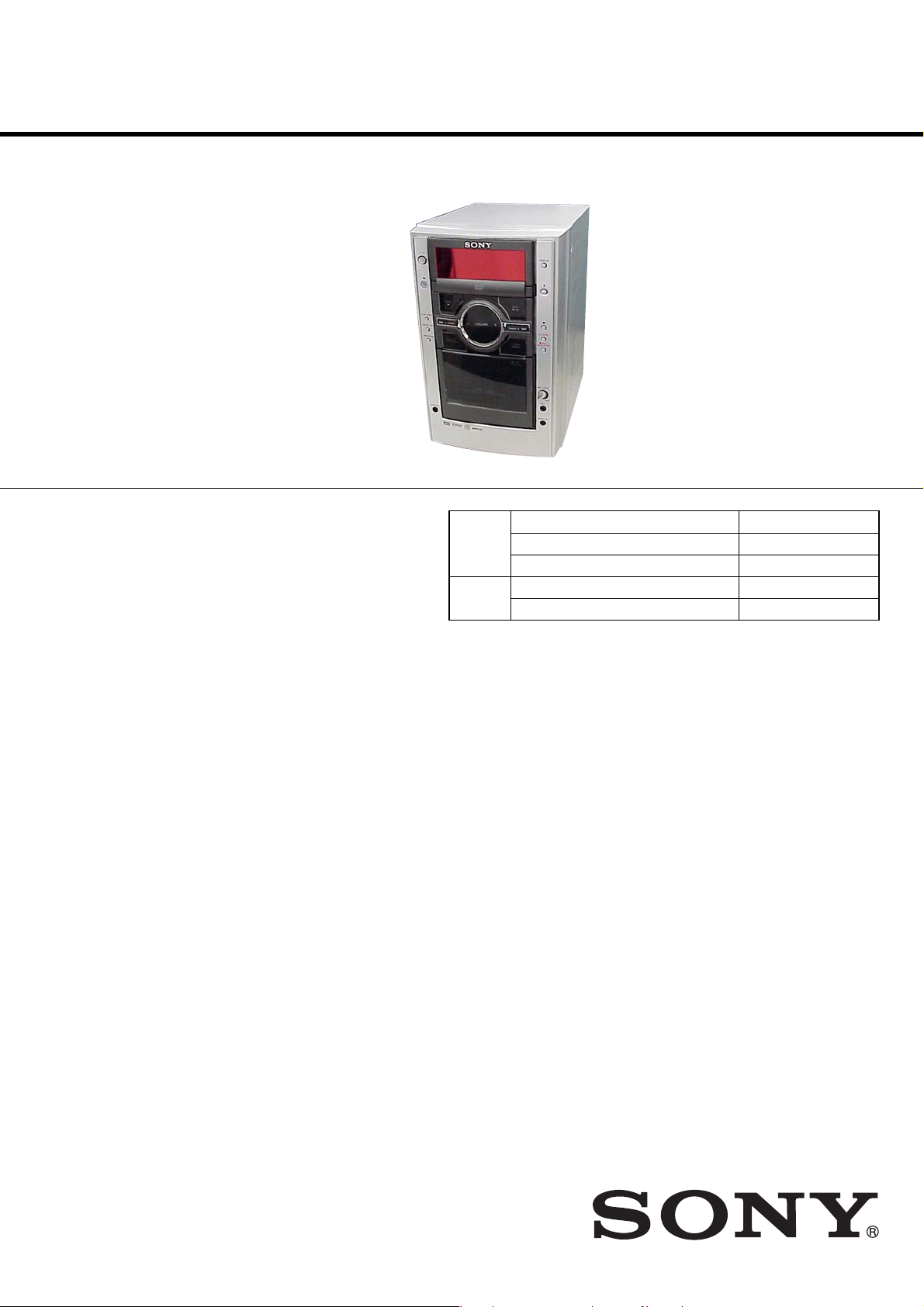
HCD-AZ1D
SERVICE MANUAL
Ver. 1.0 2006.05
HCD-AZ1D is the Amplifier, DVD player, Tape
Deck and Tuner section in DHC-AZ1D.
This system incorporates Dolby1) Digital and DTS2) Digital
Surround System.
1)
Manufactured under license from Dolby Laboratories.
“Dolby” and the double-D symbol are trademarks of
Dolby Laboratories.
2)
Manufactured under license from Digital Theater Systems,
Inc. “DTS” and “DTS 2.0 + Digital Out” are trademarks of
Digital Theater Systems, Inc.
DVD
Section
TAPE Model Name Using Similar Mechanism HCD-DV2D
Section T ape Transport Mechanism Type CMAL5Z220C
E Model
Model Name Using Similar Mechanism NEW
DVD Mechanism Type WXD
Optical Pick-up Name DM3451-A (SF-HD65F)
Amplifier section
The following measured at AC 120 V, 240 V, 50/60 Hz
DIN power output (rated): 40 + 40 watts
Continuous RMS power output (reference):
Inputs
TV IN (phono jacks): voltage 1 V, impedance
AUDIO IN (stereo mini jack):
MIC (phone jack): sensitivity 1 mV,
Outputs
VIDEO OUT (phono jack): max. output level 1 Vp-p,
COMPONENT VIDEO OUT:
(6 ohms at 1 kHz, DIN)
50 + 50 watts
(6 ohms at 1 kHz, 10%
THD)
47 kilohms
voltage 1 V, impedance
47 kilohms
impedance 10 kilohms
unbalanced, Sync
negative, load impedance
75 ohms
Y: 1 Vp-p, 75 ohms
B
, PR: 0.7 Vp-p, 75 ohms
P
SPECIFICATIONS
DIGITAL OUT (OPTICAL) (Square optical connector
jack, rear panel)
Wavelength 660 nm
PHONES (stereo mini jack):
SPEAKER: accepts impedance of
Disc player section
System Compact disc and dig it a l
Laser Semiconductor laser
Frequency response DVD (PCM 48 kHz):
Video color system format
accepts headphones of
8ohms or more
6ohms
audio and video system
(DVD: λ=650 nm,
CD: λ=790 nm)
Emission duration:
continuous
2 Hz – 22 kHz (±1 dB)
CD: 2 Hz – 20 kHz (±1 dB)
NTSC, PAL
Tape deck section
Recording system 4-track 2-channel stereo
Frequency response 40 – 13,000 Hz, using
Sony TYPE I cassette
Tuner section
FM stereo, FM/AM superheterodyne tuner
FM tuner section
Tuning range 87.5 – 108.0 MHz
(50 kHz step)
Antenna FM lead antenna
Antenna terminals 75 ohms unbalanced
Intermediate frequency 10.7 MHz
AM tuner section
Tuning range 530 – 1,710 kHz
(with the tuning interval
set at 10 kHz)
531 – 1,602 kHz
(with the tuning interval
set at 9 kHz)
Antenna AM loop antenna
Antenna terminals External antenna terminal
Intermediate frequency 450 kHz
— Continued on next page —
9-887-243-01
2006E1678-1
© 2006.05
DVD DECK RECEIVER
Sony Corporation
Home Audio Division
Published by Sony Techno Create Corporation
Page 2

HCD-AZ1D
General
Power requirements 110 – 120 V, 220 – 240 V
Power consumption
Dimensions (w/h/d) (excl. speakers)
Mass (excl. speakers) Approx. 6.1 kg
Design and specifications are subject to change
without notice.
AC, 50/60 Hz
Adjustable with voltage
selector
120 watts
Approx. 190 × 300 ×
335 mm
Laser component in this product is capable of emitting radiation
exceeding the limit for Class 1.
This appliance is classified as
a CLASS 1 LASER product.
The CLASS 1 LASER
PRODUCT MARKING is
located on the rear exterior.
CAUTION
Use of controls or adjustments or performance of procedures
other than those specified herein may result in hazardous radiation
exposure.
Notes on chip component replacement
• Never reuse a disconnected chip component.
• Notice that the minus side of a tantalum capacitor may be
damaged by heat.
Flexible Circuit Board Repairing
• Keep the temperature of the soldering iron around 270 °C
during repairing.
• Do not touch the soldering iron on the same conductor of the
circuit board (within 3 times).
• Be careful not to apply force on the conductor when soldering
or unsoldering.
UNLEADED SOLDER
Boards requiring use of unleaded solder are printed with the leadfree mark (LF) indicating the solder contains no lead.
(Caution: Some printed circuit boards may not come printed with
the lead free mark due to their particular size)
: LEAD FREE MARK
Unleaded solder has the following characteristics.
• Unleaded solder melts at a temperature about 40 °C higher
than ordinary solder.
Ordinary soldering irons can be used but the iron tip has to be
applied to the solder joint for a slightly longer time.
Soldering irons using a temperature regulator should be set to
about 350 °C.
Caution: The printed pattern (copper foil) may peel away if
the heated tip is applied for too long, so be careful!
• Strong viscosity
Unleaded solder is more viscou-s (sticky, less prone to flow)
than ordinary solder so use caution not to let solder bridges
occur such as on IC pins, etc.
• Usable with ordinary solder
It is best to use only unleaded solder but unleaded solder may
also be added to ordinary solder.
SAFETY-RELATED COMPONENT WARNING!!
COMPONENTS IDENTIFIED BY MARK 0 OR DOTTED LINE
WITH MARK 0 ON THE SCHEMATIC DIAGRAMS AND IN
THE PARTS LIST ARE CRITICAL TO SAFE OPERATION.
REPLACE THESE COMPONENTS WITH SONY PARTS WHOSE
PART NUMBERS APPEAR AS SHOWN IN THIS MANUAL OR
IN SUPPLEMENTS PUBLISHED BY SONY.
2
Page 3

TABLE OF CONTENTS
HCD-AZ1D
1. SERVICING NOTES ................................................ 4
2. GENERAL ................................................................... 7
3. DISASSEMBLY
3-1. Disassembly Flow ........................................................... 10
3-2. Top Cover, DC Fan.......................................................... 11
3-3. AMP Board, AV Board, Tuner (FM/AM) ....................... 11
3-4. MPEG Board ................................................................... 12
3-5. MPEG Holder.................................................................. 12
3-6. DVD Panel Tray .............................................................. 13
3-7. DVD Loader (WXD)....................................................... 13
3-8. Optical Pick-up DM3451-A (SF-HD65F)....................... 14
3-9. Front Panel Section ......................................................... 14
3-10. Cassette Mechanism Deck (CMAL5Z220C) .................. 15
3-11. KEY Board ...................................................................... 15
3-12. HP Board, MIC CONTROL Board ................................. 16
3-13. MAIN Board.................................................................... 16
3-14. POWER Board ................................................................ 17
3-15. Panel Cass........................................................................ 17
4. TEST MODE ............................................................... 18
5. MECHANICAL ADJUSTMENTS......................... 19
6. ELECTRICAL ADJUSTMENTS .......................... 19
7. DIAGRAMS
7-1. Block Diagram — MPEG-1 Section — ......................... 22
7-2. Block Diagram — MPEG-2 Section — ......................... 23
7-3. Block Diagram — USB Section —................................ 24
7-4. Block Diagram — AUDIO Section — ........................... 25
7-5. Block Diagram — PANEL/POWER Section — ............ 26
7-6. Printed Wiring Board — MAIN Section — ................... 27
7-7. Schematic Diagram — MAIN Section (1/4) —............. 28
7-8. Schematic Diagram — MAIN Section (2/4) —............. 29
7-9. Schematic Diagram — MAIN Section (3/4) —............. 30
7-10. Schematic Diagram — MAIN Section (4/4) — ............. 31
7-11. Printed Wiring Board — MPEG Section (Side A) — .... 32
7-12. Printed Wiring Board — MPEG Section (Side B) — .... 33
7-13. Schematic Diagram — MPEG Section (1/3) — ............ 34
7-14. Schematic Diagram — MPEG Section (2/3) — ............ 35
7-15. Schematic Diagram — MPEG Section (3/3) — ............ 36
7-16. Printed Wiring Boards — KEY Section —.................... 37
7-17. Schematic Diagram — KEY Section — ........................ 38
7-18. Schematic Diagram — MIC CONTROL Section — ..... 39
7-19. Printed Wiring Board — AV Section — ......................... 40
7-20. Schematic Diagram — AV Section — ........................... 40
7-21. Printed Wiring Board — AMP Section — ..................... 41
7-22. Schematic Diagram — AMP Section — ........................ 42
7-23. Printed Wiring Board — POWER Section —................ 43
7-24. Schematic Diagram — POWER Section — .................. 44
8. EXPLODED VIEWS
8-1. Overall Section ................................................................ 55
8-2. Front Panel Section ......................................................... 56
8-3. Chassis Section................................................................ 57
8-4. DVD Mechanism Deck Section ...................................... 58
9. ELECTRICAL PARTS LIST .................................. 59
3
Page 4
HCD-AZ1D
SECTION 1
SERVICING NOTES
NOTES ON HANDLING THE OPTICAL PICK-UP
BLOCK OR BASE UNIT
The laser diode in the optical pick-up block may suffer electrostatic
break-down because of the potential difference generated by the
charged electrostatic load, etc. on clothing and the human body.
During repair, pay attention to electrostatic break-down and also
use the procedure in the printed matter which is included in the
repair parts.
The flexible board is easily damaged and should be handled with
care.
NOTES ON LASER DIODE EMISSION CHECK
The laser beam on this model is concentrated so as to be focused on
the disc reflective surface by the objective lens in the optical pickup block. Therefore, when checking the laser diode emission,
observe from more than 30 cm away from the objective lens.
DISC TRA Y LOCK
The disc tray lock function for the antitheft of an demonstration
disc in the store is equipped.
Procedure :
1. Press the ?/1 button to turn the set ON.
2. Press the DVD u button to select “DVD”
3. Set disc on the tray, press the x button and the Z button
simultaneously for five seconds.
4. The message “LOCKED” is displayed the tray is locked.
5. To release from this mode, press the x button and the Z
button simultaneously for five seconds again.
6. The message “UNLOCKED” is displayed and the tray is
unlocked.
Note: When “LOCKED” is displayed, the slot lock is not released by
turning power on/off with the ?/1 button.
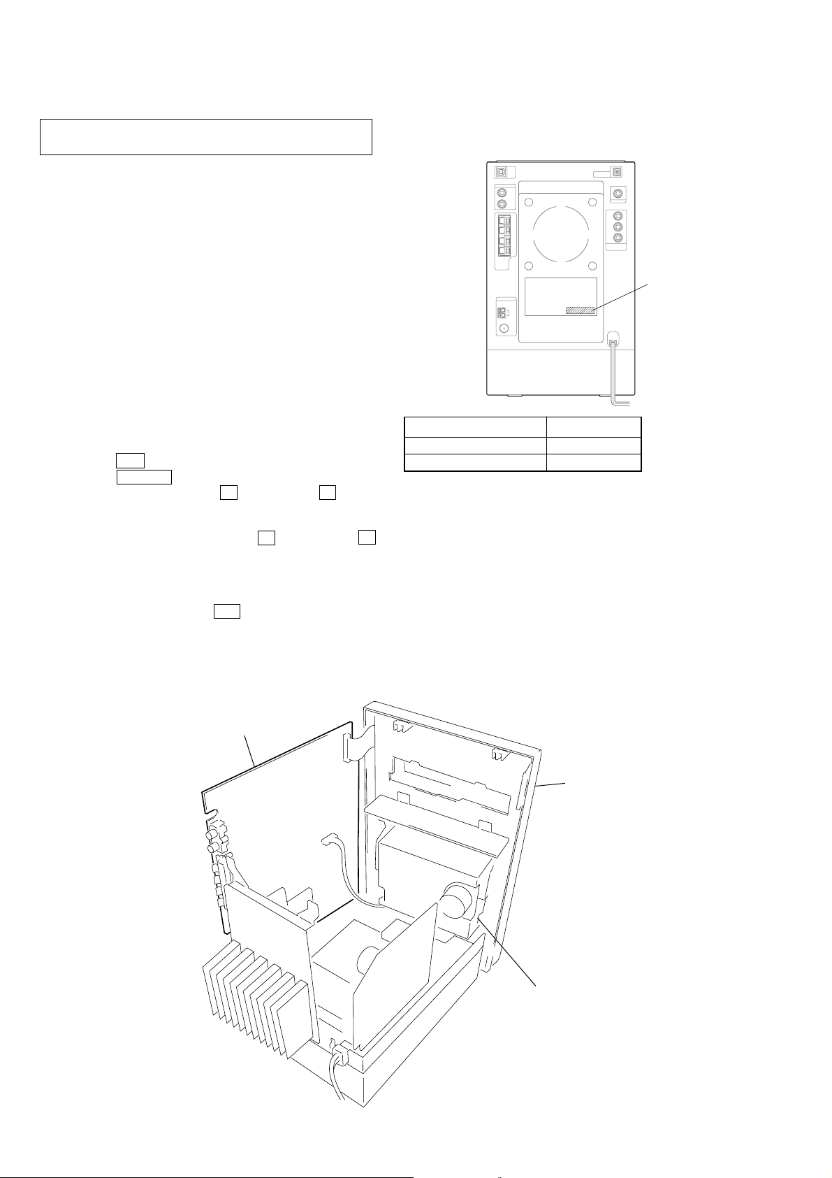
MODEL IDENTIFICATION
– Rear Panel –
Parts No.
Model Part No.
E3 model 2-672-998-0[]
SP model 2-673-001-0[]
•Abbreviation
E3 : 240 V AC Area in E model.
SP : Singapore model.
• SERVICE POSITION OF THE TAPE CASSETTE MECHANISM DECK
MAIN board
Front Panel
Tape Cassette Mechanism Deck
(CMAL5Z220C)
4
Page 5
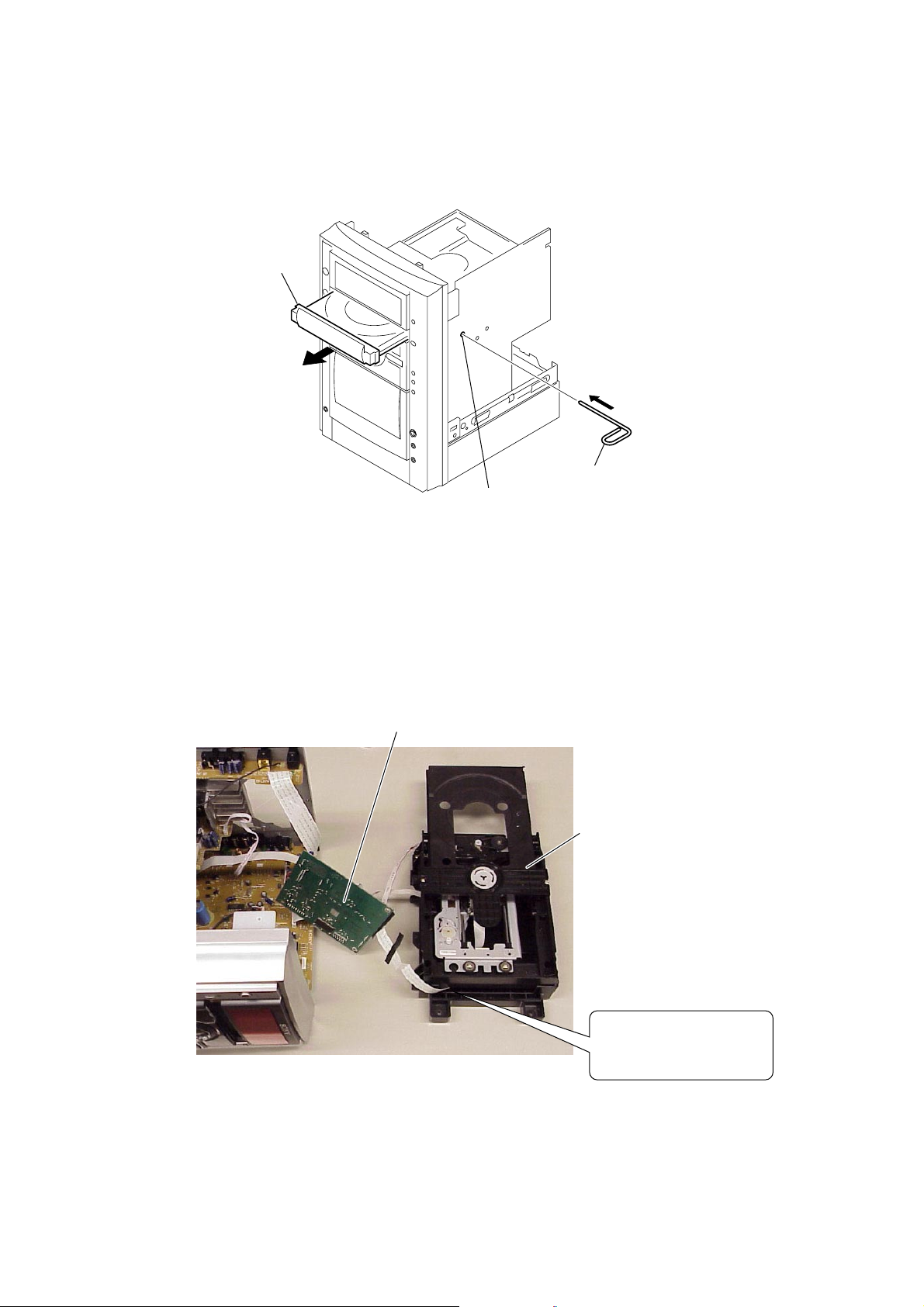
• HOW TO OPEN THE DVD TRAY MANUALLY
Insert the stiff wire in the hole. The lock is released and the DVD tray opens.
DVD tray
hole
HCD-AZ1D
stiff wire
• SERVICE POSITION OF THE DVD MECHANISM DECK
MPEG board
DVD mechanism deck
Draw out the flexible board
of the DVD mechanism deck
from this position.
5
Page 6
HCD-AZ1D
• CAUTION ON HANDLING POWER CORD (SAFETY STANDARD)
When you remove or replace the power cord,
(1) Fix the power cord to the POWER board with a binding strap as before.
(2) Check that the single-sheathed portion of the power cord does not contact the transformer
even when the single-sheathed portion is pushed toward the transformer with a 200-g force.
single-sheathed portion
of the power cord
power transformer
6
Page 7
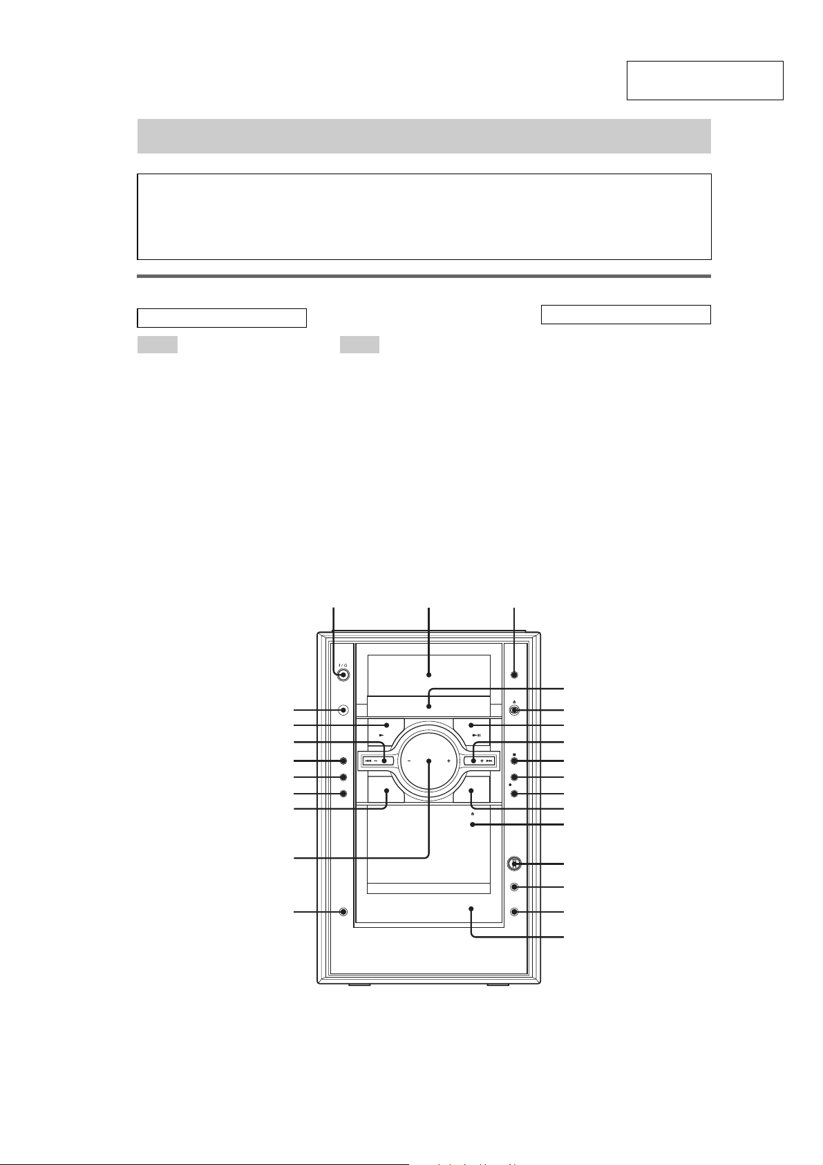
SECTION 2
GENERAL
List of button locations and reference pages
HCD-AZ1D
This section is extracted
from instruction manual.
How to use this page
Use this page to find the location of buttons and other
parts of the system that are mentioned in the text.
Main unit
ALPHABETICAL ORDER
A – O P – Z
AUDIO IN jack qg (31, 42, 43)
Cassette compartment qh (30)
CD SYNC 9 (30)
Disc tray 4 (13)
DISPLAY 3 (36, 37, 38)
Display window 2
MIC jack qf (32)
MIC LEVEL qd (32)
PC/TV/AUDIO IN ql (31, 40,
43)
PHONES jack qj
PLAY MODE ws (14, 18, 49)
PRESET EQ wa (32)
PROGRESSIVE w; (23)
Remote sensor wg
TUNER/BAND qa (27, 28, 31)
TUNING + 7 (27, 29)
TUNING – wd (27, 29)
VOLUME +/– qk (14, 29, 30, 40,
43)
Illustration number
r
TUNER/BAND qa (27, 28, 31)
RR
Name of button/part Reference page
BUTTON DESCRIPTIONS
?/1 (on/standby) 1 (10, 40, 49)
Z (open/close) 5 (13)
DVD NX (play/pause) 6 (13,
31, 44, 49)
> (go forward) 7 (14, 31)
x (stop) 8 (11, 14, 23, 28, 30,
33, 44, 49)
z REC PAUSE/START (record)
q; (30, 33)
Z PUSH OPEN/CLOSE (eject)
qs (30)
. (go back) wd (14, 31)
TAPE N (play) wf (30)
wg
wf
wd
ws
wa
w;
ql
qk
qj
12
3
4
5
6
7
8
9
0
qa
qs
qd
qf
qg
qh
7
Page 8
HCD-AZ1D
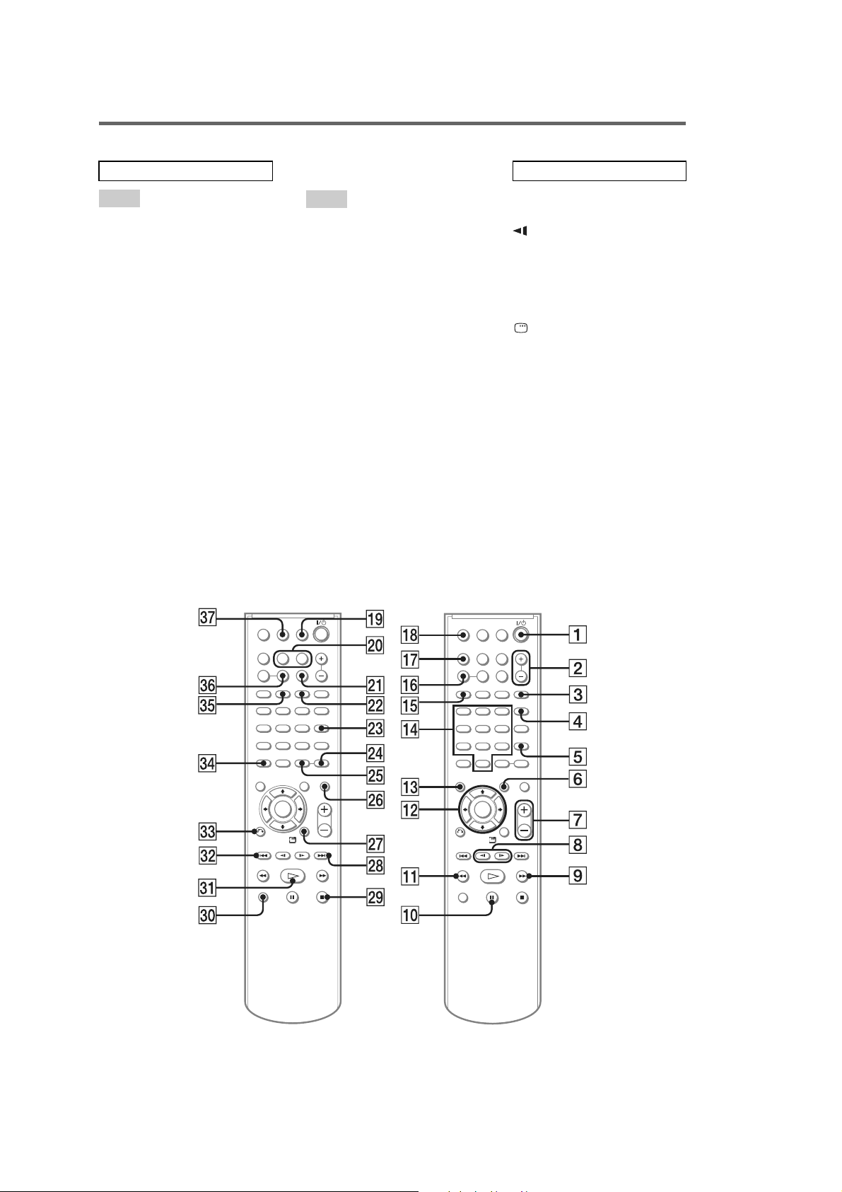
Remote control
ALPHABETICAL ORDER
A – O
ANGLE 5 (21)
AUDIO 4 (20, 32)
CLEAR ef (18, 19, 24)
CLOCK/TIMER SELECT w;
(35, 36)
CLOCK/TIMER SET w; (12, 34,
35)
DIMMER ej (36)
DISPLAY qj (36, 37, 38)
DVD eh (11, 12, 13, 16, 18, 23,
25, 30, 44)
ENTER qs wg (12, 15, 16, 18, 19,
21, 22, 24, 27, 34, 35, 43, 49)
FM MODE eg (29)
FUNCTION +/– 2 (11, 12, 13,
16, 18, 23, 25, 30, 44)
MENU 6 (15, 16)
MUTING wh (14, 29, 30)
Number buttons* qf (15, 16, 18,
19, 24, 41)
P – Z
PLAY MODE qg (14, 18)
PRESET + wk (27, 28)
PRESET – es (27, 28)
PRESET EQ wf (32)
REPEAT eg (17)
SEARCH 3 (19)
SLEEP qk (34)
SUBTITLE wd (21)
TAPE qh (30)
THEATRE SYNC ql (41)
TOP MENU qd (15)
TUNER/BAND wa (27, 28)
TUNER MEMORY ws (27)
TUNING + 9 (27, 29)
TUNING – qa (27, 29)
TV e; (40)
TV CH + wk (40, 41)
TV CH – es (40)
TV/VIDEO qk (40, 41)
TV VOL +/–* 7 (40)
VOLUME +/–* 7 (14, 29, 30,
34)
BUTTON DESCRIPTIONS
?/1 (on/standby) 1 (10, 34, 49)
TV ?/1 1 (40)
SLOW/SLOW y 8 (14)
M (fast forward) 9 (14, 30)
X (pause) 0 (14)
m (rewind) qa (14, 30)
M/m/</, qs (12, 14, 21, 43,
49)
DISPLAY wj (12, 21, 43, 49)
> (forward) wk (12, 14, 31, 34)
x (stop) wl (11, 14, 23, 30, 44)
H (play)* ea (13, 30, 44)
. (go back) es (12, 14, 31, 34)
O RETURN ed (16)
-/-- ef
*The H, number 5 and
VOLUME + (TV VOL +)
buttons have tac tile dots. Use
the tactile dots as references
when operating the system .
8
Page 9

Setting the clock
Use buttons on the remote for the operation.
1
Press ?/1 to turn on the system.
2
Press CLOCK/TIMER SET.
3
Press . or > repeatedly to set the
hour.
4
Press ENTER.
5
Press . or > repeatedly to set the
minute.
6
Press ENTER.
The clock start s working.
To adjust the clock
1
Press CLOCK/TIMER SET.
2
Press . or > to select “CLOCK SET,”
then press ENTER.
3
Do the same procedures as step 3 to 6
above.
HCD-AZ1D
Notes
•The clock settings are canceled when you disconnect
the power cord or if a power failure occurs.
•You cannot set the clock in Power Saving Mode
(page 36).
9
Page 10
HCD-AZ1D
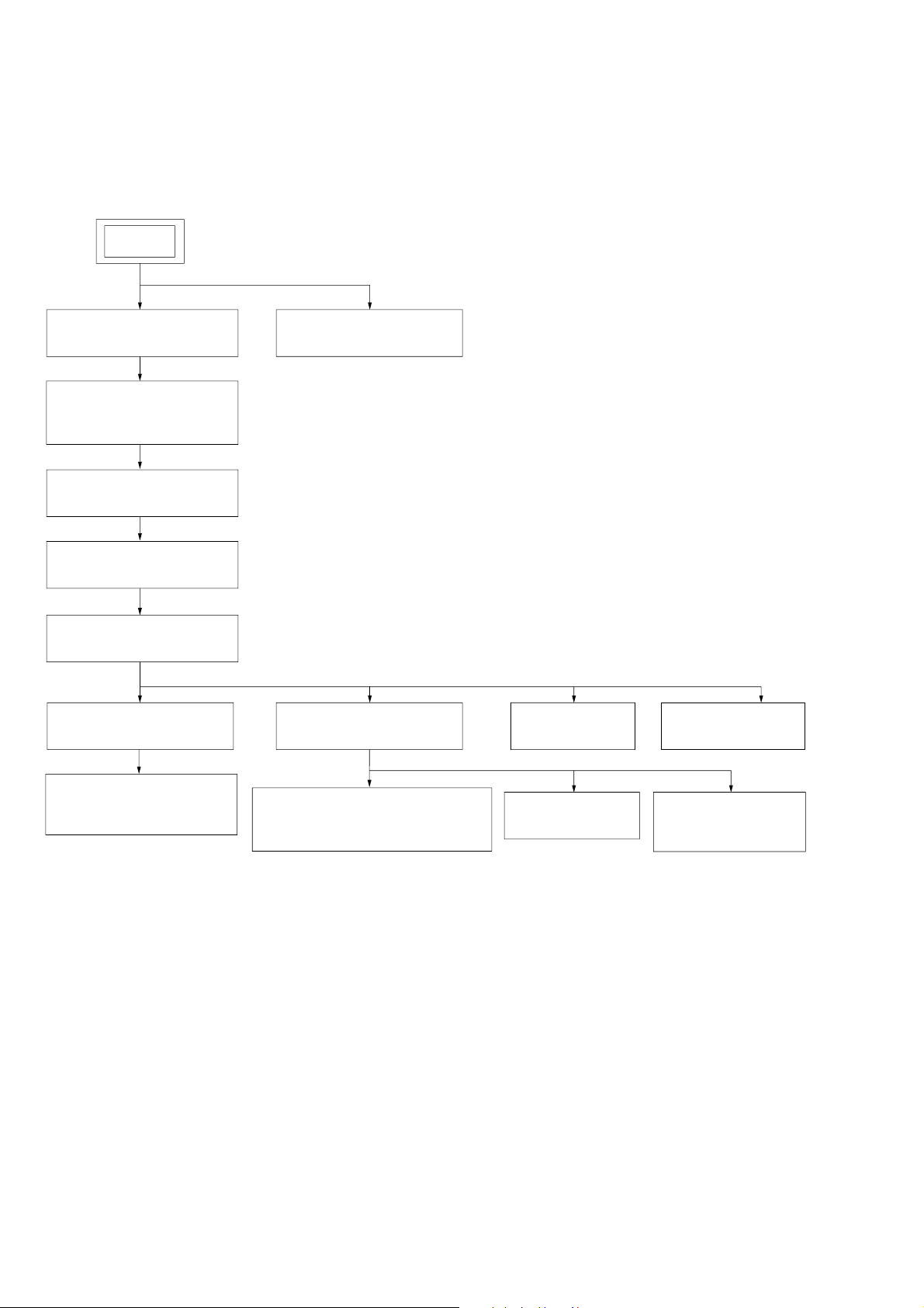
3-1. DISASSEMBLY FLOW
•This set can be disassembled in the order shown below.
SET
SECTION 3
DISASSEMBLY
3-2. TOP COVER, DC FAN
(Page 11)
3-3. AMP BOARD, AV BOARD,
TUNER (FM/AM)
(Page 11)
3-4. MPEG BOARD
(Page 12)
3-5. MPEG HOLDER
(Page 12)
3-6. DVD PANEL TRAY
(Page 13)
3-7. DVD LOADER (WXD)
(Page 13)
3-15. PANEL CASS
(Page 17)
3-9. FRONT PANEL SECTION
(Page 14)
3-13. MAIN BOARD
(Page 16)
3-14. POWER BOARD
(Page 17)
3-8. OPTICAL PICK-UP
DM3451-A (SF-HD65F)
(Page 14)
3-10. CASSETTE MECHANISM DECK
(CMAL5Z220C)
(Page 15)
3-11. KEY BOARD
(Page 15)
3-12. HP BOARD,
MIC CONTROL BOARD
(Page 16)
10
Page 11
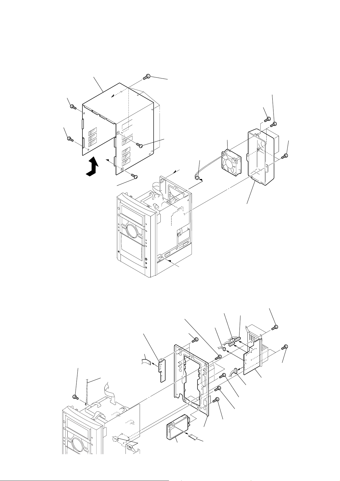
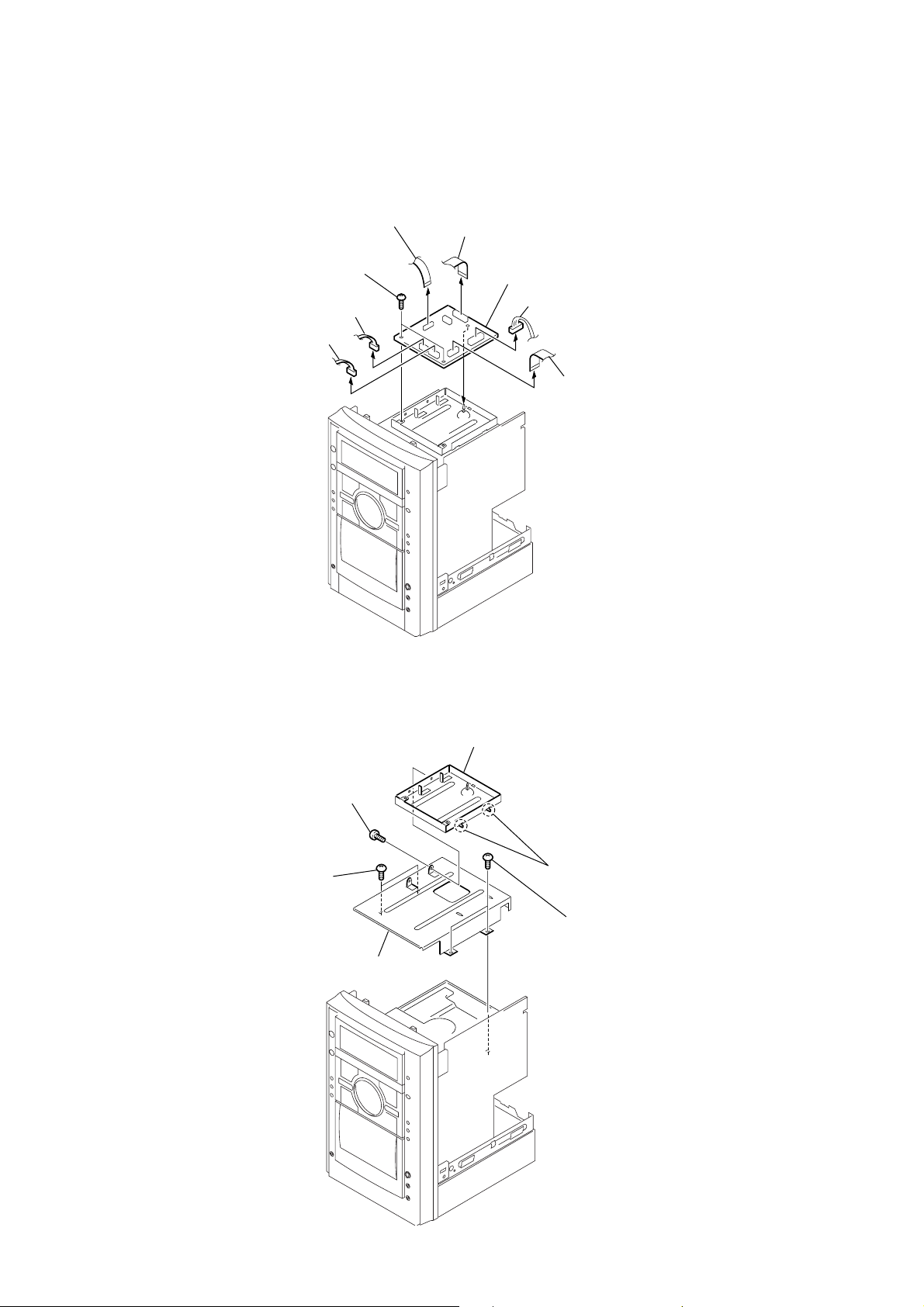
Note: Follow the disassembly procedure in the numerical order given.
3-2. TOP COVER, DC FAN
7
top cover
4
s
crew
(screw 3
3
s
(screw 3
crew
×
10)
×
6)
a
b
5
five s
(screw 3
2
s
crew
(screw 3
8
3P (CN350)
crews
×
6)
×
10)
connector
HCD-AZ1D
qa
four s
crew
crews
×
8)
×
8)
q;
two s
crews
×
(screw 3
8)
(screw 3
9
s
(screw 3
qd
DC fan
6
1
s
crew
×
(screw 3
6)
3-3. AMP BOARD, AV BOARD, TUNER (FM/AM)
0
two s
(screw 3
qf
qg
AV board
four s
(screw 3
crews
crews
×
a
b
×
8)
5
3P (CN106)
10)
4
connector
7P (CN102)
connector
qs
cover heat sink
1
two s
(screw 3
3
connector
10P (CN108)
crews
×
10)
qa
s
crew
(screw 3
qd
wire (flat type)
16core (CN801A)
×
8)
qs
earth wire
ql
two claws
qk
tuner
w;
rear panel
qj
wire (flat type)
9core
9
(screw 3
8
two s
(screw 3
qh
two s
(screw 3
crews
2
(screw 3
7
AMP board
6
connector
5P (CN101)
three s
crews
×
10)
crews
×
8)
×
8)
two s
crews
×
10)
11
Page 12
HCD-AZ1D
3-4. MPEG BOARD
7
two s
(screw 3
2
connector
5P (CN9)
1
connector
6P (CN10)
3
wire (flat type)
24core (CN7)
crews
×
8)
4
wire (flat type)
16core (CN2)
9
8
MPEG board
connector
5
9P (CN3)
6
wire (flat type)
12core (CN1)
3-5. MPEG HOLDER
1
s
crew
(screw 3
5
two s
crews
(screw 2.6
3
MPEG holder
×
8)
2
two hooks
×
8)
4
(screw 2.6
6
holder
two s
crews
×
8)
12
Page 13
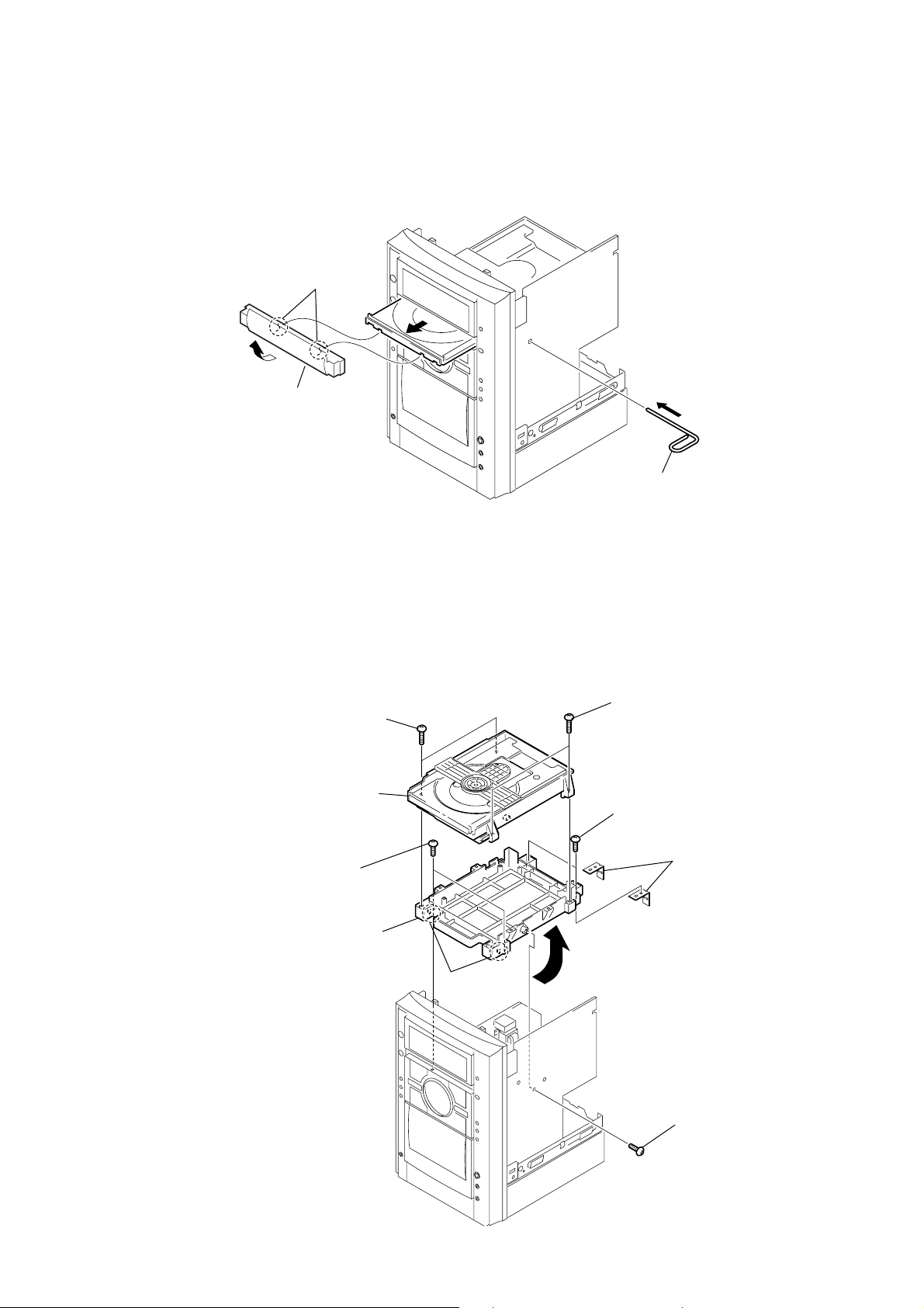
3-6. DVD PANEL TRAY
3
two
HCD-AZ1D
claws
2
4
DVD panel tray
3-7. DVD LOADER (WXD)
5
(screw 3
7
DVD loader (WXD)
two s
crews
× 10
1
stiff wire
6
two s
crews
)
(screw 3
8
two s
(screw 3
× 10
crews
×
)
10)
2
two s
(screw 3
crews
q;
DVD holder
× 10
9
two rear mecha holders
)
4
3
two dowels
1
s
crew
(screw 3
×
10)
13
Page 14
HCD-AZ1D
3-8. OPTICAL PICK-UP DM3451-A (SF-HD65F)
qa
optical pick-up
DM3451-A
9
two dumpers
(traverse mech)
8
holder (traverse mech)
3
belt (pulley)
1
Turn round the gear in the
direction of the arrow.
7
(SF-HD65F)
6
4
two screws
5
two dumpers (traverse mech)
q;
w
24core
ire (flat type)
2
3-9. FRONT PANEL SECTION
6
screw
(screw 3
×
8)
5
1
wire (flat type)
21core (CN501)
screw
(screw 3
2
connector
3P (CN202)
×
8)
qa
3
connector
8P (CN201)
claw
4
connector
3P (CN104)
q;
claw
8
screw
(screw 3
×
8)
14
9
screw
(screw 3
×
10)
qs
front panel section
7
screw
(screw 3
×
8)
Page 15
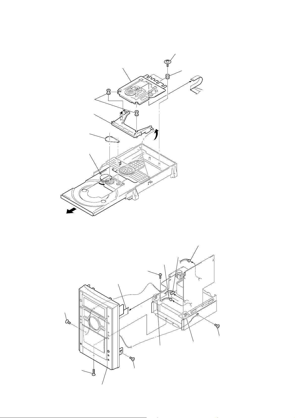
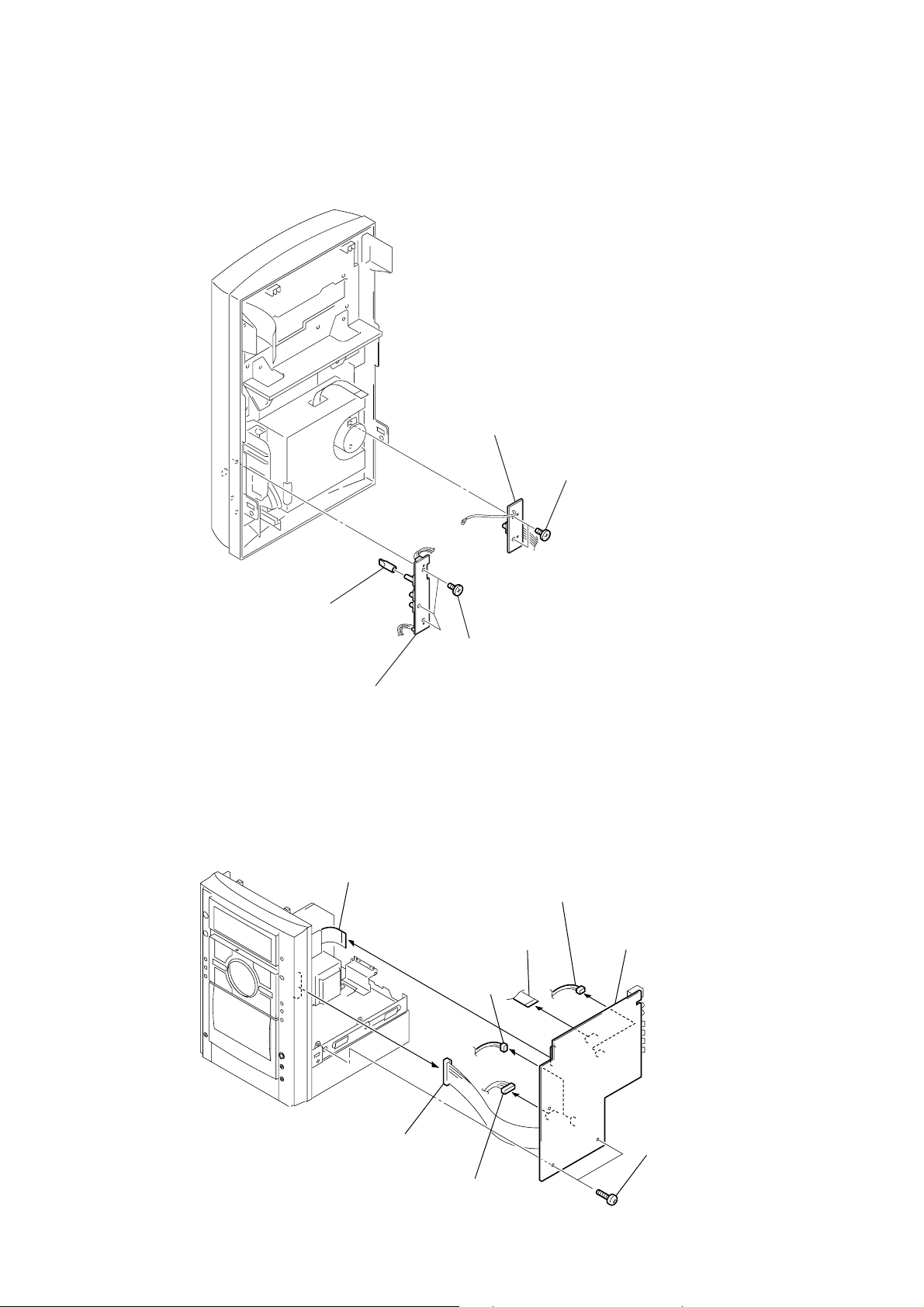
3-10. CASSETTE MECHANISM DECK (CMAL5Z220C)
1
wire (flat type)
7core
4
cover cass deck DV2D
HCD-AZ1D
3-11. KEY BOARD
5
cassette mechanism deck
(CMAL5Z220C)
4
7core (CN602)
w
ire (flat type)
3
coating clip
2
four screws
(screw 3
×
10)
3
ten screws
(screw 2.6 × 8)
5
w
ire (flat type)
21core (CN601)
6
KEY board
2
holder mecha front
1
four screws
(screw 3 × 10)
15
Page 16
HCD-AZ1D
3-12. HP BOARD, MIC CONTROL BOARD
2
HP board
1
two screws
(screw 2.6
×
8)
3-13. MAIN BOARD
4
mic knob
7
21core (CN501)
5
MIC CONTROL board
wire (flat type)
3
three screws
(screw 2.6 × 8)
5
wire (flat type)
12core (CN503)
4
connector
3P (CN202)
6
connector
3P (CN104)
8
MAIN board
16
2
connector
11P (FW901)
3
connector
8P (CN201)
1
two s
(screw 3
crews
×
10)
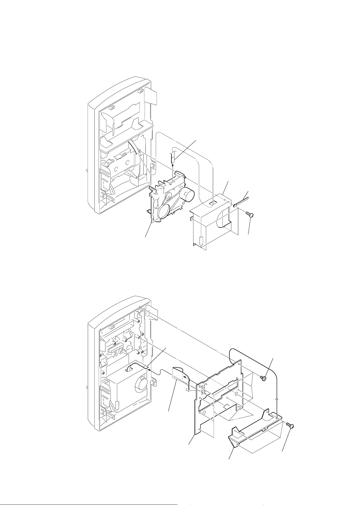
Page 17
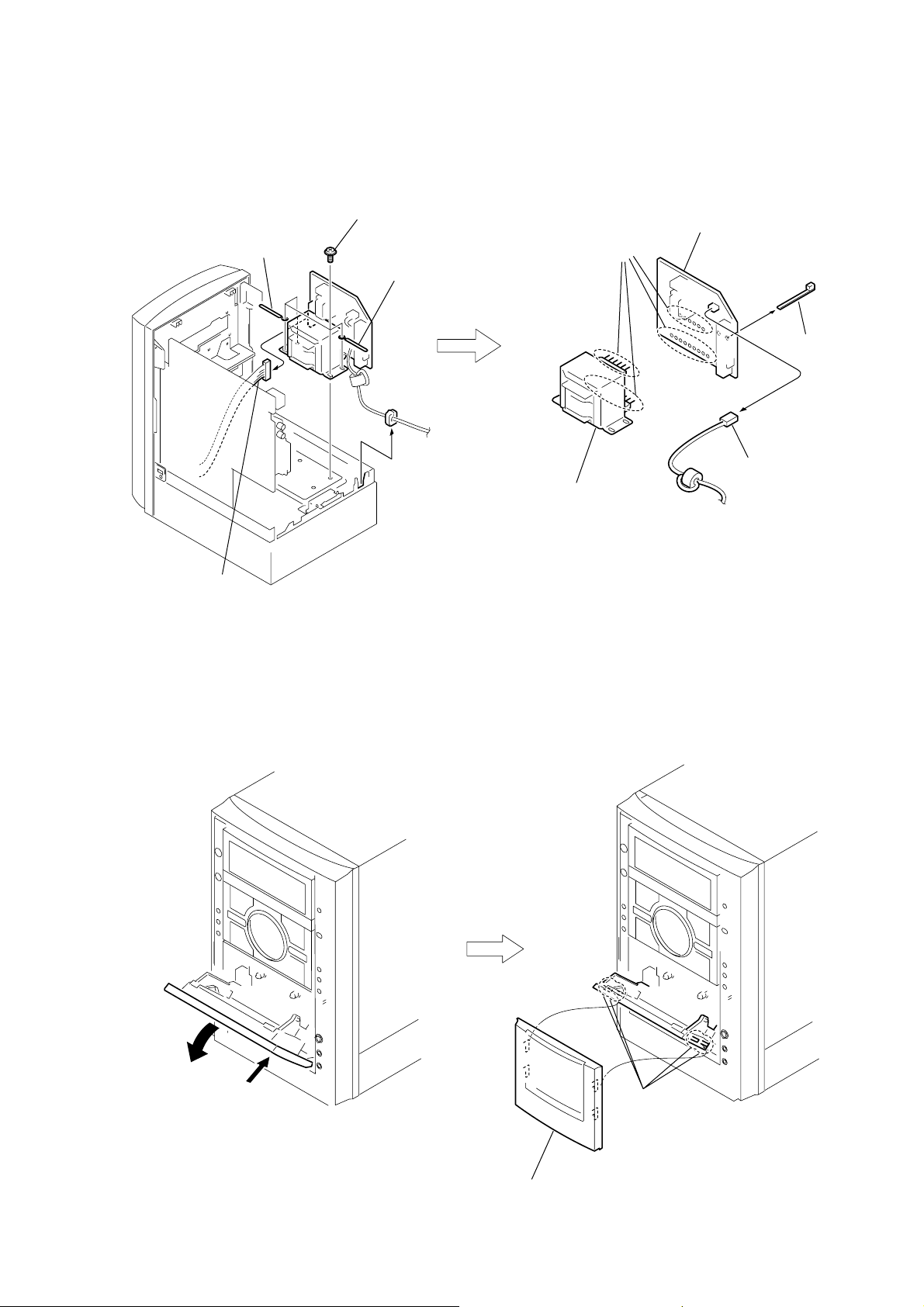
2
four screws
(screw 4
×
8)
4
coating clip
3
coating clip
9
power transformer
q;
POWER board
8
Remove the
solderings.
6
clamp
7
power cord
5
bushing cord
1
connector
11P (FW901)
3-14. POWER BOARD
HCD-AZ1D
3-15. PANEL CASS
2
1
4
panel cass, window cass
3
four claws
17
Page 18

HCD-AZ1D
SECTION 4
TEST MODE
Note 1:Regarding the notification symbol “R”
Because the number of the operating buttons of this product are
limited, some operations require use of the operating buttons of
the remote commander. When a specific operation requires use
of the operating buttons of the remote commander, “R” is added
to the specific operating procedure in this manual. Example
MENU/NO “R” The MENU/NO button of remote commander .
Note 2:Incorrect operations may be performed if the test mode is not
entered properly.
In this case, press the ?/1 button to turn the power off, and
retry to enter the test mode.
COLD RESET
• The cold reset clears all data including preset data stored in
the RAM to initial conditions. Execute this mode when
returning the set to the customers.
Procedure:
1. Press the ?/1 button to turn the set ON.
2. Press three buttons x , [PLAY MODE] and DVD u simul-
taneously.
3. The message “COLD RESET” is displayed and the set is reset.
TUNER STEP CHANGE
•A step of AM channels can be changed over between 9 kHz
and 10 kHz.
Procedure:
1. Press the ?/1 button to turn the set ON.
2. Select the function “TUNER”, and press [TUNER/BAND]
button to select the BAND “AM”.
3. Press the ?/1 button to turn the set OFF.
4. Press the x and [TUNER/BAND] buttons simultaneously,
and thus the channel step is changed over.
PANEL TEST MODE
•This mode is used to check the software version, FL, LED
and KEY.
Procedure:
1. Press the ?/1 button to turn the set ON.
2. Press the DVD u button to select “DVD”
3. Press three buttons x , [PRESET EQ] and T APE N simul-
taneously.
4. When the panel test mode is activated, all segments are turned
on.
VERSION DISPLAY
•This mode is used check the model, destination, software
version.
Procedure:
1. Press the ?/1 button to turn the set ON.
2. Press the DVD u button to select “DVD”
3. Press three buttons x , [PRESET EQ] and [TV] simultaneous-
ly, the model and destination are displayed.
DVD COLOR SYSTEM CHANGE OVER
•The color system can be changed over NTSC or PAL.
Procedure:
1. Press the ?/1 button to turn the set ON.
2. Set the function to “DVD”.
3. Press the ?/1 button to turn the set OFF.
4. Press the x button and ?/1 button simultaneously . The set
will power on automatically.
5. The message “COLOR PAL” or “COLOR NTSC” will be
displayed on the fluorescent indicator tube. The color system
is changed over.
SHIP RESET
Procedure:
1. Press the ?/1 button to turn the set ON.
2. Press the DVD u button to select “DVD”
3. Remove the disc.
4. The message “NO DISC” is displayed.
5. Press three buttons x , [PLAY MODE] and TAPE N si-
multaneously.
6. The message “SHIP RESET” is displayed and the set is reset.
The DVD function is activated.
7. To e xit from this mode, press the ?/1 button and pull out the
AC plug.
DISC TRA Y LOCK
The disc tray lock function for the antitheft of an demonstration
disc in the store is equipped.
Procedure :
1. Press the ?/1 button to turn the set ON.
2. Press the DVD u button to select “DVD”
3. Set disc on the tray, press the x button and the Z button
simultaneously for five seconds.
4. The message “LOCKED” is displayed the tray is locked.
5. To release from this mode, press the x button and the Z
button simultaneously for five seconds again.
6. The message “UNLOCKED” is displayed and the tray is
unlocked.
Note: When “LOCKED” is displayed, the slot lock is not released by
turning power on/off with the ?/1 button.
CD REPEAT 5 TIMES LIMIT RELEASE MODE
Procedure:
1. Press the ?/1 button to turn the set ON.
2. Set the function to “DVD”.
3. Press three buttons x , Z , and DVD u simultaneously.
4. The repeat all mark blinks and then repeat 5 times limit is
released.
18
Page 19
SECTION 5
MECHANICAL ADJUSTMENTS
HCD-AZ1D
SECTION 6
ELECTRICAL ADJUSTMENTS
Precaution
1. Clean the following parts with a denatured alcohol-moistened
swab:
record/playback heads pinch rollers
erase head rubber belts
capstan idlers
2. Demagnetize the record/playback head with a head demagnetizer.
3. Do not use a magnetized screwdriver for the adjustments.
4. After the adjustments, apply suitable locking compound to
the parts adjusted.
5. The adjustments should be performed with the rated power
supply voltage unless otherwise noted.
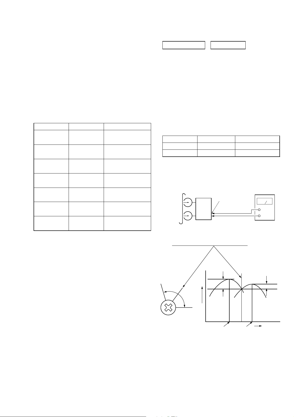
Torque Measurement
Mode
FWD
FWD
back tension
REV
REV
back tension
FF/REW
FWD tension
REV tension
Torque meter Meter reading
2.94 – 7.84 mN • m
CQ-102C
CQ-102C
CQ-102RC
CQ-102RC
CQ-201B
CQ-403A
CQ-403R
(31 to 71 g • cm)
(0.43 – 0.98 oz • inch)
0.15 – 0.59 mN • m
(2 to 6 g • cm)
(0.02 – 0.08 oz • inch)
2.94 – 7.84 mN • m
(30 to 79 g • cm)
(0.42 – 1.11 oz • inch)
0.15 – 0.59 mN • m
(2 to 6 g • cm)
(0.03 – 0.08 oz • inch)
6.86 – 17.64 mN • m
(71 to 143 g • cm)
(0.98 – 2.49 oz • inch)
9.8 mN • m or more
(100 g • cm or more)
(1.4 oz • inch or more)
9.8 mN • m or more
(100 g • cm or more)
(1.4 oz • inch or more)
DECK SECTION 0 dB=0.775V
1. Demagnetize the record/playback head with a head
demagnetizer.
2. Do not use a magnetized screwdriver for the adjustments.
3. After the adjustments, apply suitable locking compound to
the parts adjusted.
4. The adjustments should be performed with the rated power
supply voltage unless otherwise noted.
5. The adjustments should be performed in the order given in
this service manual. (As a general rule, playback circuit
adjustment should be completed before performing recording
circuit adjustment.)
6. The adjustments should be performed for both L-CH and RCH.
7. Switches and controls should be set as follows unless otherwise
specified.
Signal Used forTape
P-4-A100
WS-48B
[Record/Playback Head Azimuth Adjustment]
Procedure:
1. Mode : Playback
test tape
P-4-A100
(10kHz, –10dB)
2. Turn the adjustment screw and check output peaks. If the peaks
do not match for L-CH and R-CH, turn the adjustment screw
so that outputs match within 1 dB of peak.
10 kHz, –10 dB
3 kHz, 0 dB
MAIN board
JK102
speaker terminal
set
Azimuth Adjustment
Tape Speed Adjustment
level meter
+
–
L-CH
peak
screw
position
R-CH
peak
output
level
within
1 dB
L-CH
peak
R-CH
peak
within 1dB
screw
position
19
Page 20

HCD-AZ1D
3. Mode: Playback
test tape
P-4-A100
(10kHz, –10dB)
in phase 45
MAIN board
JK102
speaker terminal
L
set
R
Waveform of oscilloscope
good
°
90
135
°
oscilloscope
°
180
wrong
°
4. After the adjustments, apply suitable locking compound to
the parts adjusted.
Adjustment Location: Record/Playback/Erase Head
DVD SECTION
[RF Level Check]
Check the RF level when optical pick-up block is replaced.
Connection:
oscilloscope
MPEG board
8
CN7 pin
CN7 pin
Procedure:
1. Connect an oscilloscope to CN7 pin 8 (V-RF) and CN7 pin
wf (GND) on the MPEG board.
2. Turn the power on.
3. Set the test disc on the tray and press DVDu button to
playback.
4. Observe the waveform of the oscilloscope, and check that the
RF level is satisfied to specified value.
[Test Disc List and Specified Value]
Use the following test disc on adjustment.
CD YEDS-18 (Part No.: 3-702-101-01)
PATD-012 (Part No.: 4-225-203-01)
DVD SL (Single Layer)
NTSC :HLX-503 (Part No.: J-6090-069-A)
HLX-504 (Part No.: J-6090-088-A)
PAL : HLX-506 (Part No.: J-6090-077-A)
DVD DL (Dual Layer)
NTSC :HLX-501 (Part No.: J-6090-071-A)
HLX-505 (Part No.: J-6090-089-A)
PAL : HLX-507 (Part No.: J-6090-078-A)
Note: Do not use existing test disc for DVD.
(V-RF)
wf
(GND)
TEST DISC Specified Value
+
–
0.57 to 1.1 Vp-p
0.58 to 1.23 Vp-p
adjustment screw
Note: Refer to “ 3-15. PANEL CASS ” (see page 17)
[Tape Speed Check]
Procedure:
1. Turn the power on.
2. Insert the WS-48B into deck.
3. Press the TAPE N button of deck.
4. Check the reading of frequency counter becomes 3000 ± 90
Hz.
Sample Value of Wow and flutter
W.RMS (JIS) less than 0.3%
(test tape: WS-48B)
Checking Location: MPEG board (Side A)
— MPEG Board (SIDE A) —
CN7
1
23
CN7 Pin
IC6
wf
24
(GND)
CN7 Pin
U2
2
8
(V-RF)
IC4
IC7
20
Page 21

SECTION 7
DIAGRAMS
HCD-AZ1D
THIS NOTE IS COMMON FOR PRINTED WIRING BOARDS AND SCHEMATIC DIAGRAMS.
(In addition to this, the necessary note is printed in each block.)
For Schematic Diagrams.
Note:
• All capacitors are in µF unless otherwise noted. (p: pF)
50 WV or less are not indicated except f or electrolytics and
tantalums.
• All resistors are in Ω and 1/
specified.
• f : internal component.
• C : panel designation.
Note: The components identified by mark 0 or dotted
line with mark 0 are critical for safety.
Replace only with part number specified.
• A : B+ Line.
• B : B– Line.
•Voltages and waveforms are dc with respect to ground
under no-signal (detuned) conditions.
– MPEG Section –
No mark: DVD STOP
– Other Section –
No mark: FM
( ) : TAPE REC
•Voltages are taken with a VOM (Input impedance 10 MΩ).
Voltage variations may be noted due to normal production
tolerances.
•Waveforms are taken with a oscilloscope.
Voltage variations may be noted due to normal production
tolerances.
• Circled numbers refer to waveforms.
• Signal path.
F : AUDIO
d : TUNER
j : PB (TAPE)
a : REC (TAPE)
J : DVD/CD (AUDIO)
I : DVD/CD (DIGITAL)
: DVD (RF)
h : TV IN
i : AUDIO IN
L : VIDEO
g : CD (RF)
r : COMPONENT
E : Y
: USB
N : MIC
•Abbreviation
E3 : 240 V AC Area in E model
SP : Singapore model
4
W or less unless otherwise
For Printed Wiring Boards.
Note:
• X : parts extracted from the component side.
• Y : parts extracted from the conductor side.
• f : internal component.
•
• Indication of transistor.
: Pattern from the side which enables seeing.
Caution:
Parts face side: Parts on the parts face side seen from
(Side A) the parts face are indicated.
Pattern face side: P arts on the pattern face side seen from
(Side B) the pattern face are indicated.
C
Q
B
E
B
B
These are omitted.
CE
These are omitted.
Q
CE
These are omitted.
• Circuit Boards Location
MPEG board
KEY board
MAIN board
HP board
MIC CONTROL board
POWER board
AV board
AMP board
HCD-AZ1D
2121
Page 22

HCD-AZ1D
7-1. BLOCK DIAGRAM — MPEG-1 SECTION —
OPTICAL
PICK-UP BLOCK
DM3451-A
(SF-HD65F)
VR-CD
VR-DVD
F-
F+
T+
T-
A
B
C
D
E
F
VS
F-
F+
T+
T-
VR CONTROLLER
VR CONTROLLER
Q4,11
(CD)
Q10
(DVD)
160
162
165
167
170
172
186
185
171
168
176
188
177
173
A
B
C
D
E
F
ICI05
ICI04
K
J
CD-MD
IDI03
DVD-MD
VC
U2(1/2)
RF AMP
FOCUS/TRACKING
ERROR AMP
MDA0-15
MAD0-19
35,37,39,42
MWR#
RESET#
15,17,28,31,
34,36,38,40,
MCS#0
MRD#
9,11,14,16
18,19,22,24
26,27,30,33
23
141
4-8,10,13,
43,45,46,
48,49
47
44
FLASH MEMORY
28-36,
DQ0-15
38-45
11
WE
12
RP
1-9,
16-25,
A0-18
48
OE
28
CE
26
IC6
LD(DVD)
LD(CD)
OPEN SW
CLOSE SW
LOAD+
HOME SW
SPIND+
SPIND-
PANEL/POWER
SECTION
(Page 26)
PANEL/POWER
SECTION
(Page 26)
V-RF
LOAD-
SLED+
SLED-
RFP
157
Q2
POWER
CONTROLLER
(DVD)
Q21
POWER
CONTROLLER
(CD)
F-
F+
T+
TOP
TCL
T-
D
C
179
178
DVD_LD
CD_LD
OPN
CLS
IO32
IO46/PWNCO5
IDI04/PWNCO6
183
200
+3.3V
VOFC-
13
VOFC+
14
VOTK+
15
VOTK-
16
PLHD
10
PVCC1
9
12
VOSL+
VOSL-
11
VOLD+
17
VOLD-
18
V/VFFC
7
VOSL
6
IC7
MOTOR
DRIVER
STBY
VINSL-
CF CERR1
CF CERR2
CTKERR1
VINSL+
VINFC
VINTK
VINLD
28
5
2
3
25
4
1
26
23
+1.8V
Q16
+3.3VREG
Q17
+1.8VREG
+5V
201
I04/PWNCO0
202
IO43/PWNCO2
195
198
IO45/PWNCO4
• Signal Path
: DVD(RF)
: CD(RF)
HCD-AZ1D
2222
Page 23

7-2. BLOCK DIAGRAM — MPEG-2 SECTION —
PANEL/POWER
SECTION
(Page 26)
E
DSSTB
DSCK
DSDA
MRST
1
SSCTXD/IO17
IO47/SSCCLK
207
IO16/SSCTXD
208
RESET#
141
IC14
EEPROM
SDA
5 6
135
136
IC103//VIDO
SCL
IC031
137
IDI02
IC501(1/4)
SYSTEM CONTROLLER
8
VIDEO SW
XO
143
GCLK
144
CVBS/C
150
CVBS/C/Y
148
151V/R/Y
C/B/V
153
Y1
27MHz
Y
PB/CB
PR/CR
JK803A
PB/C
PR/C
Y
B
R
HCD-AZ1D
COMPONENT
VIDEO OUT
RCS#O
RBA0
PCLK
70
71
80 73
RBA0
RCSO
PCLK
19
18
35 15 16 17 14 36
CS
A11
CLK
VIDEO DAC ENCODER
RWE#
RCAS#
RRAS#
77
75
74
78
RWE
RCAS
RRAS
RDQM
WE
CAS
RAS
U2(2/2)
RDQM#
RCS1
LDOM
UDOM
RCS#1
SDRAM
88-90,92,94,96,
98-100,102-104
2,3,5,6,8,9,11,
12,39,40,42,43,
IC4
RDAT0-15
82,84-86,
45,46,48,49
D0-D15
DAT0-15
DAT0-15
RADD1-10
53-57,59,60,
61,63,65,67
20-24,
27-32
A0-A10
ADD1-10
ADD1-10
SPDIF
AB CLK
AMCLK
ALR CLK
AOUT O
110
116
118
115
113
2
SCLK
4
MCLK
3
LRCK
1
SDATA
RCS1
PCLK
RBA0
19
RWE
RCAS
18 35 15 16 17 14 36
CS
WE
A11
CLK
CAS
AUDIO DAC
RRAS
RDQM
RAS
LDOM
U4
AOUTL
AOUTR
UDOM
SDRAM
8
5
2,3,5,6,8,9,11,
12,39,40,42,43,
IC5
45,46,48,49
D0-D15
R-CH
DAT0-15
20-24,
27-32
ADD1-10
A0-A10
VOUT
2 1
IC8
AMP
JK801
VIDEO OUT
JK804A
TX
B
DIGITAL OUT
AUDIO
SECTION
(Page 25)
OPTICAL
• R-CH is omitted due to same as L-CH.
• Signal Path
: DVD/CD(AUDIO)
: DVD/CD(DIGITAL)
: VIDEO
: COMPONENT
: Y
HCD-AZ1D
2323
Page 24

HCD-AZ1D
7-3. BLOCK DIAGRAM — USB SECTION —
JK201
L
TV IN
R
JK601
R-CH
AUDIO IN
R-CH
IC402
QUAD ANALOG
IC401
USB I/F
DA CONVERTER
1
J401
USBVCC
USBBD-
PC
USBBD+
USBGND
Q401,412
USB MUTE
Q413
USB MUTE
21
HOST
D-
8
9
D+
DGND
6
Q414
USB MUTE
VOUTL
VOUTR
XT0
XT1
14
R-CH
15
Q402
SWITCH
1
X401
12MHz
28
Q403,404
SWITCH
Q405
MUTE
I1
4
I2
5
C2
6
C3
13
C1
12
C4
SWITCH
2
O1
3
O2
Q410
MUTE
Q407
SWITCH
Q408,409
SWITCH
1
4
5
6
13
12
QUAD ANALOG
I1
I2
C2
C3
C1
C4
IC403
SWITCH
O1
2
3
O2
F
AUDIO
SECTION
(Page 25)
43
U-SENS
64
PCON
58
USB PS
IC501(2/4)
SYSTEM CONTROLLER
57
AUXTUS
R-CH is omitted due to same as L-CH.
Signal path
:USB
:TV IN
:AUDIO IN
HCD-AZ1D
2424
Page 25

7-4. BLOCK DIAGRAM — AUDIO SECTION —
HCD-AZ1D
SECTION
(Page 24)
ANTENNA
USB
F
MIC
FM 75Ω
COAXIAL
AM
JK202
MIC LEVEL
TUNER PACK
L-CH
R-CH
D OUT
D IN
CL
CE
SO
R-CH
3
+
-
2
IC250(1/2)
MIC AMP
VR250
IC302
MPEG-2
SECTION
(Page 23)
1
5
4
19
18
20
12
11
IC250(2/2)
MIC AMP
7
+
-
IC501(3/4)
SYSTEM CONTROLLER
SDAT/ROMDA
SCK/ROM CK
TUDO
TUDI
TUCK
TUCE
STE
STRB
AMUT
TSOL
TMOT
TCNT
REPT
HDPN
RPHD
BIAS
52
53
54
59
5
6
7
31
30
3
4
IC201
AMP
B
Q322
MUTE CONT
Q321
MUTE CONT
SOUND PROCESSOR
CD-L
21
19
23
7
2
13
5
6
AUX-L
TUNER-L
VOL-IL
TAPE-L
COMT
REC-O-L
SDA
SCL
Q105
MUTE CONT
OUT-L
18
28
IC503
EPROM
R-CH
A
PANEL/POWER
SECTION
(Page 26)
Q102
MUTE
INH
MUTE
+VDD
Q319
MUTE
SWITCH
Q314,317
CURRENT
+9V(TU)
DETECT
IC103
POWER AMP
CH1_
CH1_
11 4
IN
OUT+
STBY
13
Q199
INVERTER
Q308
PROTECT
SWITCH
Q104,301
OVER LOAD
DETECT
R-CH
Q303,304,354
DC PROTECT
R-CH
R-CH
R-CH
L
R
Q350-352
FAN CONT
Q353,355
FAN CURRENT
DETECT
JK104
PHONES
JK102
SPEAKER
IMPEDANCE
USE 6Ω
DC
FAN
MECHANISM
REC/PB
HEAD
ERASE
TAPE
DECK
L-CH
R-CH
PACK
RECF
RECR
HDPLY
TCNT
MOT
SOL
R-CH
R-CH
T301
Q653,654
MOTOR DRIVER
Q651,652
SOL DRIVER
Q327,332
REC/PB SWITCH
Q329-331
REC/PB SWITCH
Q344-Q347
OSC
+VM
Q348
• R-CH is omitted due to same as L-CH.
• Signal Path
: AUDIO
: PB(TAPE)
: REC(TAPE)
: TUNER
: DVD/CD(AUDIO)
: TV IN
: MIC
HCD-AZ1D
2525
Page 26

HCD-AZ1D
7-5. BLOCK DIAGRAM — PANEL/POWER SECTION —
IC501 (4/4)
SYSTEM CONTROLLER
VFSTB
VFCK
VEDA
IC651
FL DRIVER
GRID1-4
14-29,
31-38
42-39
17
16
15
SEG1-SEG24
9
STB
8
CLK
7
DIN
VFD651
FLUORESCENT
INDICATOR
TUBE
VF
VF
VF
PT901
POWER
TRANSFORMER(MAIN)
S667,S651-654,S657
FUNCTION
KEY
S665,S666,S656,S658,S659
FUNCTION
KEY
S655,S660-664
FUNCTION
KEY
REMOTE
CONTROL
RECEIVER
IR651
1
X501
32.768kHz
X502
8.38MHz
30
-33V(VPP)VEE
13
VDPVDD
Q601
LED1
1
KEY3
28
KEY2
27
LED
KEY1
26
PCON
INH
REM
45
TUON
37
XT2
38
XT1
40
X2
41
X1
CD ON
Q502
LED
60
DRIVE
64
44
61
62
D652
LED2
2
I/
LED
DRIVE
Q602
LED
DRIVE
D601-D604
D605-D608
VF
AUDIO
SECTION
(Page 25)
SWITCH
A
Q306
INH
MUTE
SWITCH
+9V (TU)
Q196,197
SWITCH
Q318
+6V
Q305,Q320
POWER
CONTROL
Q309,310
SWITCH
Q198
+9V
REG
IC101
+6V
REG
-33V(VPP)
D309
D324
D +5V
+12V(VM)
+9V
+10V
D319 - D321
Q315
-33V
REG
POWER AMP B+
POWER AMP B-
+VDD
IC301
+5V
2
REG
5
Q311,312
+12V
REG
Q316
+9V
REG
Q313
REG
D306
D301
D302
1
MPEG-1
SECTION
(Page 22)
MPEG-1
SECTION
(Page 22)
MPEG-2
SECTION
(Page 23)
RY901
C
D
E
CLS
OPN
TOP
TCL
DSCK
DSSTB
DSDA
MRST
CLS
56
OPN
55
14
TOP
35
TCL
DSCK
50
DSSTB
49
DSDA
48
MRST
47
RLY
FPON
RST
AVR
SFTY
63
Q504-506
+5V
REG
+12V(VM)
D501
D901-904
VDP
23
IC502
RESET
36
SWITCH
34
29
Q507
SWITCH
D503
+5V
D906
Q307
RELAY
DRIVE
TRANSFORMER
D907
PT902
POWER
(SUB)
SW901
VOLTAGE
SELECTOR
AC IN
HCD-AZ1D
2626
Page 27

HCD-AZ1D
7-6. PRINTED WIRING BOARD — MAIN SECTION —
12
A
MAIN BOARD
B
A
KEY BOARD
C
CN601
(Page 37)
E
SFTY
E
D
TAPE
MECHANISM
DECK
HEAD
REC/PB
HEAD
L-CH
R-CH
ERASE
HEAD
(REC/PLAYBACK/ERASE)
1
2
3
4
5
6
7
8
E
E
A
A
E
F
81
G
K
MIC
H
CONTROL
BOARD
CN250
(Page 37)
• See page 21 for Circuit Boards Location.
345678910 11
MPEG BOARD
CN1
for DOWN LOAD
28
1
1
2
20
21
7
IC501
49
48
E
E
8
5
1
4
64
1
16 17
(Page 33)
33
32
BL
1
11
2
12
IC502
8
5
R218A
R220A
1
8
L409
7
4
IC503
R447
R444
R441
JR401
IC403
Q407
R439
E
R434
Q409
E
E
R438
Q411
Q408
E
14
Q410
R437
R436
R451
E
1
L410
R440
C426
E
E
Q
Q347
E
2
E
A
E
1
E
E
IC302
E
E
E
E
E
R266
R249
EE
R264
R246
C259
5
8
C262
R268
IC201
R265
R263
C221
C220
4
R247
C260
1
R267
R248
C261
CN
E
E
E
3
1
202
1
E
5
R435
C425
3
R432
D404
C412
C420
JR402
R431
C421
R430
Q406
R426
Q405
E
R425
R420
R412
C417
R413
L408
L407
R120A
R118A
4
1
C409
R433
C419
C410
R428
R421
C422
R427
C418
R429
R416
7
E
1
14
R414
L405
IC402
R418
8
MIC CONTROL BOARD
CN603
(Page 37)
C120
C232
D405
C411
R417
C413
C416
R419
R415
C415
C436
R455
R456
R457
R458
R422
R409
E
R445
Q403
JR405
R459
Q402
Q404
R423
R424
C414
15
28
IC401
R408
C401
C402
C440
D406
E
R410
E
R411
C406
14
X401
D401
TUNER
R407
L411
L412
R406
R405
C439
L414
L415
5
2
3
1
4
6
J401
PC
MPEG BOARD
C
CN3
(Page 33)
R118
R218
+
–
–
+
1
10
8
2
1
9
E
E
E
E
9
Q412
Q401
R404
E
E
C403
R401
R442
C405
L403
C404
L401
1
FB401
C438
R403
C407
Q413
E
E
C430
C437
Q414
1
3
C100
C132
IC101
1
C105
CN105
1
3
E
IC301
E
E
1
7
L
IN
R
AMP BOARD
CN106
(Page 41)
L
SPEAKER
IMPEDANCE USE 6Ω
R
H
AMP BOARD
CN108
(Page 41)
JK201
TV
E
JK102
• Semiconductor Location
Ref. No.
D105 G-9
D106 C-10
D107 C-10
D196 B-9
D198 B-8
D199 B-8
D301 I-5
D302 I-3
D305 G-5
D306 I-3
D307 I-2
D308 H-3
D309 J-4
D310 H-2
D312 G-9
D313 G-5
D314 G-9
D317 G-9
D318 G-2
D319 F-7
D320 F-7
D321 F-7
D323 I-7
D324 J-4
D325 H-4
D330 C-8
D401 E-7
D404 D-6
D405 C-7
D406 E-7
D501 G-5
D502 D-3
D503 C-3
D505 D-2
D507 F-5
D508 H-3
IC101 C-8
IC201 G-3
IC301 H-5
IC302 F-4
IC401 D-7
IC402 E-6
IC403 E-5
IC501 B-4
IC502 C-3
IC503 D-5
Location
Ref. No.
Q196 B-9
Q197 B-9
Q198 B-8
Q199 B-9
Q305 J-4
Q306 I-2
Q307 H-3
Q313 G-8
Q315 I-3
Q316 H-3
Q317 H-5
Q318 G-5
Q319 J-3
Q320 J-4
Q321 G-5
Q322 G-5
Q326 G-3
Q327 G-3
Q328 G-3
Q329 G-3
Q330 G-3
Q331 G-3
Q332 G-3
Q344 F-2
Q345 F-3
Q346 D-3
Q347 D-3
Q348 E-3
Q401 D-7
Q402 E-7
Q403 E-7
Q404 E-7
Q405 E-6
Q406 D-6
Q407 E-5
Q408 D-5
Q409 D-5
Q410 E-5
Q411 D-5
Q412 D-7
Q413 D-8
Q414 E-8
Q502 C-3
Q504 D-3
Q505 D-3
Q506 D-3
Q507 C-3
Location
HCD-AZ1D
E
I
E
11
E
K
K
A
E
E
A
K
A
1
I
AMP BOARD
CN102
(Page 41)
J
POWER BOARD
D
(Page 43)
FW901
(CHASSIS)
2727
Page 28

HCD-AZ1D
7-7. SCHEMATIC DIAGRAM — MAIN SECTION (1/4) —
IC501 VOLTAGE CHART
PIN.No Voltage PIN.No Voltage
1
2
3
4
5
6
7
8
9
10
11
12
13
14
15
16
17
18
19
20
21 0
22
23
24
25
26
27
28
29
30
31
32
33
34
35
36
37
38
39
40
41 2.8
4.9
42
4.9
43
4,9
44
0
45
0
46
0
47
0
48
0
49
50
5
51
0
52
0
53
0
54
4.8
55
0
56
0
57
4.9
58
0
59
0.3
60
0
61
4.9
62
0.2
63
5.1
64
5
5
5
2.8
3.8
3.8
0.4
0
5
0
5
3.3
2.4
0
3
0
4.9
4.9
0
4.9
3.2
3.4
4.8
0.3
0
4.9
4.9
0
0
4.9
0
4.9
0
0
4.9
4.9
4.9
A
KEY
BOARD
CN601
(Page 38)
B
MPEG
BOARD(1/3)
CN1
(Page 34)
21P
for DOWNLOAD
• See page 45 for Waveforms. • See page 48 for IC Pin Function Description.
TUNER
_
SO
MAIN BOARD
1000P
5
0.01
0.01
SWITCH
CN502
8P
12P
(1/4)
9P
1000P
1000P
5
4.2
R587
2.7K
0
7
5
5
IC502
RESET SWITCH
3.1
INVERTER
3.4
V
3.8
IC501
SYSTEM CONTROLLER
+9V REG
12.4
10
10.7
10.7 10.7
V
47K
V
8
SWITCH
0
0
SWITCH
TV
IN
( )
1000P
V
1000P
1200P
0.6
V
1200P
V
V
L
R
120K
120K
R218
2.2K
R118
2.2K
V
V
30
31
32
MAIN BOARD
3
(4/4)
(Page 31)
0.01
B
5
IC503
EP ROM
LED DRIVER
0.3
5.7
270
11.3
0.3
1K
4.9
5
4.9
0.01
+5V REG
0.7
10.6
10.3
No mark:FM
( ):REC
0.6
0.2
+5V REG
+5V REG
2
134
5
789
6
13
10
HCD-AZ1D
MAIN BOARD
(2/4)
1
(Page 29)
2828
Page 29

HCD-AZ1D
7-8. SCHEMATIC DIAGRAM — MAIN SECTION (2/4) —
REC/PB
HEAD
LCH
RCH
ERASE
TAPE
MECHANISM
DECK
(REC/PB/ERASE)
MAIN BOARD
8P
(2/4)
C125
3300P
0.018
• See page 45 for Waveform. • See page 46 for IC Block Diagram.
IC302
SOUND
PROCESSOR
IC B/D
3300P
C225
0.018
V
C107
0
0
00000000
00000000
0
0
0000
0
4.6 -4.5 -4.5
10K
IC201
AMP
-4.5
00
0
4.5
0
0
0
V
MAIN
BOARD (1/4)
1
6
2
578
1
3
4
9
10
(Page 28)
13
34
33
MAIN
4
BOARD
35
14
10K
F
IC301
+5V REG
5.1
16.5
0
15
16
17
18
19
20
21
22
(4/4)
(Page 31)
2
MAIN BOARD
(Page 30)
(3/4)
SWITCH
0
0(6.1)
0
Q344~Q347
BIAS OSC
0(0.4)
0(0.4)
10
0(6.2)
16
0(-6.2)
1.9(-11.7)
S
0
0(-6.2)
0
2.1(-6.5)
0
0
2.1(-6.5)
1.9(-11.9)
S
2.2(0)
2.2(0)
2.2(-11)
S
1.9(-11.9)
Q329~Q332,
Q326,Q327
REC/PB SWITCH
JR101
0
2.1(-6.6)
16
0.6
9
0(6.1)
0
SWITCH
0(6.8)
0
0(9.6)
0.6
9.8
9.8(8.9)
9.8(0)
SWITCH
0(2.1)
CN202
3P/2.0
10V
MIC
+
AGND
MIC CONTROL
K
(Page 39)
BOARD
CN250
MPEG BOARD
C
(Page 36)
(3/3)
CN3
C105
IC101
NJM7806FA
6
9
C100
IC101
+6V REG
0.01
0
0.6
SWITCH
23
24
No mark:FM
( ):REC
HCD-AZ1D
2929
Page 30

HCD-AZ1D
7-9. SCHEMATIC DIAGRAM — MAIN SECTION (3/4) —
5
MAIN BOARD
(4/4)
(Page 31)
MAIN BOARD
36
(3/4)
MUTE SWITCH
H
AMP
BOARD
CN108
(Page 42)
BOARD
I
(Page 42)
AMP
CN102
AMP
E
BOARD
CN106
(Page 42)
L
+
L
1000P
GND
-
GND
-
R
R
+
(IMPEDANCE USE 6 )
SPEAKER
( )
0.01
0.01
1000P
0.1
2
0
0
MAIN BOARD
(4/4)
(Page 31)
2
MAIN BOARD
(2/4)
(Page 29)
7
MAIN BOARD
(4/4)
(Page 31)
0
3.8
SWITCH
37
6
14
15
16
17
18
19
20
21
22
23
24
21
0
0
0.6
0.6
POWER
CONTROL
11
16.5
CURRENT
DETECT
9.8
16.3
POWER
CONTROL
16.6
CURRENT DETECT
0
11P
16.7
+9V REG
8.8
10.8
-32.9
-38.6
-32.4
-33V REG
RELAY
DRIVE
0
4700P
4.5
D
POWER BOARD
FW901
(Page 44)
HCD-AZ1D
No mark:FM
( ):REC
3030
Page 31

HCD-AZ1D
7-10. SCHEMATIC DIAGRAM — MAIN SECTION (4/4) —
PC
3.3
JW
JW
A
0
FB401
6
37
MAIN
BOARD(3/4)
(Page 30)
MAIN
BOARD
(3/4)
MA01
7
21
PON
Q413
DTC114YK
0
4.9
Q414
DTC114YK
R442
22K
0
(Page 30)
• See page 46 for IC Block Diagram.
MAIN BOARD
Q401,Q412
Q413,
Q414
USB MUTE
3.3
A
0
IC401
10V
(4/4)
DA CONVERTER
USB I/F
IC B/D
MTZJ3.3A
C437
V
C440
1000P
0.1U
10V
8.4
INVERTER
SWITCH
0
SWITCH
V
50V
R418
0
9.8
A
9.7
0
15K
50V
V
15K
8
470P
C417
L405
2
0
0
0
QUAD ANALOG
2
0
39K
IC402
SWITCH
IC B/D
A
Q405,Q406
0
A
MUTE
R431
C419
+
V
V
1
2
3
MIC CONTROL
L
BOARD
CN603
(Page 39)
MAIN
BOARD(1/4)
(Page 28)
M
BOARD(2/4)
N
3
4
MAIN
(Page 29)
30
R220A
120K
R120A
120K
R451
100K
0
JR401
IC403
QUAD ANALOG
SWITCH
IC B/D
2
MUTE
2
0
A
MUTE
0
A
R447
100K
Q408
Q408,
0
9.7
SWITCH
50V
50V
8.4
Q409
R444
100K
9.8
R439
0
100K
INVERTER
DTA114YKA
0
32
31
35
33
34
R118A
2.2K
R218A
2.2K
IC401,IC402,IC403
VOLTAGE CHART
Pin No Pin No
1
2
3
4
5
6
7
8
9
10
11
12
13
14
IC401
3
15
-
16
17
3.3
-
18
-
19
0
20
3.3
21
22
0
0
3.3
0
0
27
3.3
0
36
5
MAIN
BOARD(3/4)
IC402 IC403
Voltage(V)
Pin No
Voltage(V)Voltage(V)
23
24
25
26
28
1
0
22
3.3
33
0
44
0
55
0
66
3.3
0
77
88
0
99
0
0
10 10
3.3
3.3
12
13 13
0
14 14
3
Pin No
Voltage(V)
1
0
0
0
0
8.4
8.4
0
0
0
0
0
0
0
9.8
0
0
0
0
8.4
8.4
0
0
0
0
0
1111
0
12
0
9.8
No mark : FM
( ):REC
(Page 30)
HCD-AZ1D
3131
Page 32

HCD-AZ1D
7-11. PRINTED WIRING BOARD — MPEG SECTION (SIDE A) —
12
345678910111213
A
MPEG BOARD
(SIDE A)
B
C
D
E
• See page 21 for Circuit Boards Location.
OPTICAL
PICK UP
BLOCK
DM3451-A (SF-HD65F)
24
E
14
• Semiconductor
Location
Ref. No.
14
8
7
1
IC7
28
15
E
E
E
E
21
E
E
22
E
E
D2 F-4
IC4 K-7
IC6 H-4
IC7 C-11
IC8 I-11
IC14 G-11
Q2 E-7
Q4 D-9
Q5 E-11
Q7 D-11
Q10 D-9
Q11 D-8
Q21 E-7
Q22 D-11
Q23 E-11
U2 H-7
U4 I-10
Location
C150
F
12
3
208
1
157
156
G
48
25
1
4
IC14
5
H
U2
8
IC6
1
4
8
I
241
52
105
10453
1
U4
4
5
J
25
1
5
IC8
8
HCD-AZ1D
IC4
K
26
50
3232
Page 33

HCD-AZ1D
7-12. PRINTED WIRING BOARD — MPEG SECTION (SIDE B) —
12
345678910111213
A
MPEG BOARD
(SIDE B)
B
+
C
E
D
1
2
E
F
AV BOARD
CN801A
(Page 40)
F
15
16
• See page 21 for Circuit Boards Location.
for Down Load
+
+
1
4
+
+
+
+
14
• Semiconductor
Location
Ref. No.
D3 J-12
D7 J-3
D10 F-12
D12 D-3
IC5 K-8
Q16 C-2
Q17 J-5
+
+
+
+
151
Location
G
+
H
+
+
I
J
+
+
+
+
+
+
+
67
+
E
+
50
26
+
1
DVD
MECHANISM
DECK
5
1
DVD
MECHANISM
DECK
6
IC5
9
1
K
+
1
25
12
11
2
1
HCD-AZ1D
C
MAIN BOARD
CN302
(Page 27)
B
MAIN BOARD
CN503
(Page 27)
3333
Page 34

HCD-AZ1D
1000P
0.027
1000P
1000P
0.01
0.1
1000P
1000P
1000P
1.8K
4.7K
0.1
JR
0.01
0.01
0.01
0.1
0.1
0.1
1000P
1000P
4.7K
4.7K
1000P
0.1
4.7K
4.7K
7-13. SCHEMATIC DIAGRAM — MPEG SECTION (1/3) —
B
MAIN
BOARD(1/4)
CN503
(Page 28)
MPEG BOARD
for DOWN LOAD
1.8K
(1/3)
• See page 45 for Waveforms. • See page 50 for IC Pin Function Description.
0.01
3.3
3.3
3.3
3.3
U2
RF AMP
ERROR AMP
0.4
0.5
1.403.3
3.3
3.3
3.3
3.3
3.3
3.3
3.3
3.3
3.3
3.3
0
0
1.4
0.4
0.6
3.3
0.5
3.3
JR
0
2.8
3.3
3.3
3.3
0
0
0
0
3.3
3.3
3.3
3.3
3.3
0
3.3
3.3
0
0
0
1000P
0.027
IC6
FLASH MEMORY
SST39VF800A 70-4C
1000P
0
3.3
1000P
3.2
0
3.2
3.2
0
0
0
0
3.2
3.2
0
0
0
0
0
0
0
3.3
3.3
3.3
0
0
3.3
3.7
3.3
3.3
4.7K
0.1
1000P
2
0
0
0
0
0.1
3.3
3.7
0
0
3.3
0
0
1000P
0
3.3
3.3
3.3
0
0
0
0
0
0
3.3
0
0.9
3
0
0.3
3.3
2.2
1.1
3.3
2,2
0
0
0
0
1000P
3.2
0
3.2
2.3
2.2
2.2
2.4
2.5
0
0
1.4
2.3
2.5
0.9
0
0
000000000
0
0.7
3.3
3.3
3.3
3.3
VIDEO DAC ENCODER
3.3
0.7
3.303.3
3.3
ZR36862 TQFP-208
FOCUS / TRACKING
1
2
3
1
MPEG
4
BOARD(3/3)
5
6
7
12
10
11
9
8
(Page 36)
2
MPEG
BOARD(3/3)
(Page 36)
3
MPEG
BOARD(3/3)
(Page 36)
0.01
3.3
3.3
3.3
3.3
3.3 00
0.01
0
1.8
1.8
1.8
1.8
1.8
1.8
0
0
0
0
0.2
0.2
2.4
0
0
3.3
0
1.3
0.4
0.4
1.2
1.3
2.2
2.1
1.3
3.3
3.3
1
5
1.3
0
1.2
6
3
1.7
2.3
2
0
0
1.8
0
2
3.7
0
3.3
0
0
0
3.3
0
0
1000P
4.7K
AT24C0
0.01
0.1
0.1
1000P
1000P
0.1
4
4.7K
4.7K
5
0
3.3
3.3
4.7K
0.1
IC14
EEP ROM
HCD-AZ1D
14
4
MPEG
BOARD(2/3)
(Page 35)
0.7
0.5
0.5
0.8
0.8
0.800.2
IC4
SD RAM
1.2
1.1
1.2
1.1
1.5
1.1
0
0.200
0.2
K4S161622H
0
0
1.5
1.2
1.2
1.4
1.3
1.3
3.3
0
3.3
1.5
3.33.3.3 3.3
3.3
3.2
3.2
3.3
3.3
3.3
0.8
0.7
0.7
0.5
0.5
0.8
0.8
0.800.2
0.200
0.200
3.3
1.5
3.3
3.3
3.3
3.3
3.3
3.3
3.3
3.3
K4S161622H
0
0
1.2
1.1
1.2
1.1
1.5
1.1
1.5
0.8
0.7
1.3
1.4
1.2
1.2
1.3
3.3
3.3
IC5
SD RAM
No mark : DVD STOP
13
5
MPEG
BOARD(2/3)
(Page 35)
3434
Page 35

7-14. SCHEMATIC DIAGRAM — MPEG SECTION (2/3) —
MPEG
4
BOARD(1/3)
(Page 34)
14
MPEG BOARD (2/3)
5
MPEG BOARD(1/3)
(Page 34)
13
HCD-AZ1D
MPEG
6
BOARD(3/3)
(Page 36)
15
16
DVD
MECHANISM
DECK
OPTICAL
PICK-UP
BLOCK
DM3451-A
(SF-HD65F)
855D
0.1
3.3
3.3
3
0
1.3
1.3
1.7
1.3
0
0
7.1
0
0
0
3.6
3.6
0
AM5888S
2.8
1.7
1.7
7.1
1.7
7.1
7.1
2.7
2.7
3.6
3.6
IC7
MOTOR
DRIVER
0.1
0.1
0
2N3904
Q4,11
VR
CONTROLLER
(CD)
0.7
3.3K
0
0
0.7
2N3904
VR CONTROLLER
(DVD)
4.7K
0.7
2N3904
2.2K
3.3
3.1
Q2
0
POWER
CONTROLLER
(DVD)
3.3
3.1
0
Q21
POWER
CONTROLLER
(CD)
4.1
855D
+3.3V REG
3.6 1.8
6.8
+1.8V REG
4.7K
0.022
0.1
0.1
1000P
0.1
0.1
HCD-AZ1D
No mark : DVD STOP
3535
Page 36

HCD-AZ1D
7-15. SCHEMATIC DIAGRAM — MPEG SECTION (3/3) —
MPEG BOARD (3/3)
1
2
MPEG
BOARD
(1/3)
(Page 34)
MPEG
BOARD
(1/3)
(Page 34)
3
1
4
5
6
2
7
MPEG
BOARD
(1/3)
(Page 34)
F
AV BOARD
CN801A
0.1
8
Q5,7,23
BLANKOUT
5
0
(2/2)
2N3904
SWITCH
0
0.1
5
5
0.01
0.01
0.1
0.1
3
9
10
11
12
0.1
0.1
0.1
0.1
0.10.01
U4
AUDIO DAC
0
0
1.7
2
2.3
5
0
0
0.1
0.01
0.1
0.1
1000P
0.01
IC8
(1/2)
AMP
IC8 (1/2)
BA4558F
0.1
1000P
1000P
10
5
5
0
5
5
IC8(2/2)
BA4558F
IC8
AMP
CONTROL
1000P
0.1
0.1
11.3
11.3
10.6
0
0.7
8.4
0
1000P
0.1
(Page 40)
(Page 29)
C
MAIN
BOARD
(2/4)
CN302
HCD-AZ1D
16
6
15
MPEG
BOARD
(Page 35)
No mark : DVD STOP
(2/3)
3636
Page 37

HCD-AZ1D
7-16. PRINTED WIRING BOARDS — KEY SECTION —
34567 9
1
5
A
B
12
KEY BOARD
1
2
A
MAIN
BOARD
CN501
(Page 27)
C
D
DISPLAY
20
21
Z
• See page 21 for Circuit Boards Location. :Uses unleaded solder.
VFD651(FLUORESCENT INDICATOR TUBE)
10 15 20
E
E
25
IC651
33
34
30
23
22
44
1
35
12
11
40
44
8
10
HP BOARD
(STANDBY)
?/1
1
3
AMP
BOARD
CN101
(Page 41)
5
J
1
11
PHONES
• Semiconductor
Location
Ref. No.
D601 E-3
D602 G-3
D603 E-7
D604 G-7
D605 F-4
D606 F-5
D607 F-5
D608 F-6
D651 G-6
D652 B-9
D654 F-7
D655 G-4
IC250 F-10
IC651 B-6
IR651 D-9
Q601 C-4
Q602 C-4
Q651 G-6
Q652 F-6
Q653 F-8
Q654 F-8
Location
IR651
E
F
G
H
CD SYNC
x
REC
PAUSE/START
TUNING
>
TUNER/BAND
DVD
u
VOLUME
VOLUME
E
E
2
6
1
7
TAPE
MECHANISM
DECK
TAPE
N
.
TUNING
PC/TV/AUDIO IN
MIC CONTROL BOARD
K
13
E
PLAY MODE
E
PRESET EQ
PROGRESSIVE
IC250
58
1
4
MAIN BOARD
CN202
(Page 27)
MIC LEVEL
MIC
AUDIO IN
HCD-AZ1D
L
MAIN
I
1
3
3737
BOARD
CN104
(Page 27)
Page 38

HCD-AZ1D
HDPL
JR652
7-17. SCHEMATIC DIAGRAM — KEY SECTION —
KEY BOARD
IR651
REMOTE CONTROL
RECEIVER
4.9
4.9
+
VOLUME
PAUSE/START
PC/TV/AUDIO IN
REC
PROGRESSIVE
VOLUME
• See page 47 for IC Block Diagram.
100
JR650
S667
0
B
-
DISPLAY
BX
4700P
-29.2
-29.2
-29.2
-29.2
-29.2
-29.2
-29.2
-29.2
-29.2
(FLUORESCENT INDICATOR TUBE)
JR651
0
-26.5
-24.0
-29.0
-29.0
-29.0
-31.5
-29.0
-32.1
-29.2
-29.2
-29.2
-26.5
-29.0
-29.0
-31.5
uPD16315GB-3BS
IC651
FL DRIVER
4.9
IC B/D
-29.0
-29.0
-29.0
-29.0
-26.5
4.9
0
0
Q651, Q652
SOL DRIVER
9.0
0
9.4
9.0
Q653, Q654
MOTOR DRIVER
9.5
9.5
9.5
9.4
9.5
7P
TAPE
MECHANISM
DECK
HDPL
JR652
0
Y
PLAY
MODE
Q601,Q602
LED DRIVE
R603
AMBER
J
AMP
BOARD
CN101
(Page 42)
470
D601
.
470
R606
D604
AMBER
_
1.5
R609
TUNING
R607
1K
470
D605
AMBER
R610
+
TUNING
>
Q601 Q602
2SC2712GR 2SC2712GR
470
470
R604
R605
D602
D603
AMBER
AMBER
HP BOARD
Z
470
D606
AMBER
?/1
470
R611
D607
AMBER
470
R612
D608
AMBER
0.60.6
1.5
330 1/2W
330 1/2W
R608
D655
1N4001
1K
0.01
D601-D608
SLR-342VCT31
L106
FB
JR102
0
0.01
330 1/2W
330 1/2W
0
JR101
C166
4.9
JK104
4.9
CHASSIS
P203
0
1.8
4.9
4.9
0
4.9
47
D652
SLR-342VCT31
50
p
00
(STNDBY)
JR653 0
4V
No mark : FM
21P
A
MAIN BOARD (1/4)
CN501
(Page 28)
J
HCD-AZ1D
3838
Page 39

7-18. SCHEMATIC DIAGRAM — MIC CONTROL SECTION —
HCD-AZ1D
MIC
AUDIO IN
JK601
JK202
MIC CONTROL BOARD
JR251
0
R251
100K
C256
0.1
JR250
L602
L601
C650
0.1
C250
0.1
50V
R259
0
4.7K
R258
4.7K
R250
4.7K
R252
22K
C258
0.1
C251
1000P
C257
470
6.3V
C264
100P
R273
1K
IC250(1/2)
BA4558F
4.8
3
2
4.8
IC250
MIC AMP
8
+
R272
47K
(1/2)
9.8
IC250
(2/2)
MIC AMP
C268
0.01
JR252
IC250(2/2)
C265
100P
BA4558F
4.8
5
6
4.8
R256
0.1
R254
10K
R260
150
C253
1000P
C254
0.1
R255
22K
C252
0.1
4.8
1
22K
R253
250
VR
10K-B
MIC LEVEL
C266
4
+
7
150K
C255
1000P
0
CN250
3P
+10V
R257
BEAD
4.8
(SMD)
1
MIC
2
AGND
3
MAIN
K
BOARD(2/4)
CN202
(Page 29)
CN603
3P
1
R
2
L
3
AGND
MAIN
L
BOARD(4/4)
CN104
(Page 31)
WP250B
No mark : FM
HCD-AZ1D
3939
Page 40

HCD-AZ1D
7-19. PRINTED WIRING BOARD — AV SECTION —
12
AV BOARD
A
MPEG BOARD
F
(Page 33)
CN2
1
1
2
3
B
15
16
WP801A
• See page 21 for Circuit Boards Location.
:Uses unleaded solder.
3
JK804A
DIGITAL OUT
OPTICAL
JK801
VIDEO OUT
7-20. SCHEMATIC DIAGRAM — AV SECTION —
AV BOARD
A
A
FB
F
MPEG BOARD
(3/3)
CN2
(Page 36)
P /C
P /C
A
Y
BB
RR
COMPONENT
VIDEO OUT
DIGITAL OUT
OPTICAL
A
A
A
0
A
V
A
A
0
V
A
A
0
V
A
A
A
AA
A
A
A
A
A
C
D
E
Y
P /C
BB
P /C
RR
JK803A
COMPONENT
VIDEO OUT
HCD-AZ1D
4040
Page 41

HCD-AZ1D
7-21. PRINTED WIRING BOARD — AMP SECTION —
12
[AMP BOARD]
A
E
E
E
B
)
E
JW(
E
C
• See page 21 for Circuit Boards Location.
J
1
E
E
HP BOARD
CW101
(Page 37)
5
E
13
E
E
MAIN BOARD
E
(Page 27)
CN105
WP102
:Uses unleaded solder.
345
WP103
E
1
MAIN BOARD
I
7
E
E
E
E
10
E
H
E
1
E
1
CN103
(Page 27)
MAIN BOARD
CN107
(Page 27)
• Semiconductor
Location
Ref. No.
D101 C-3
D102 B-2
D103 B-2
D104 B-2
D311 C-3
D350 A-1
D352 B-1
D353 C-1
D355 C-4
IC103 D-2
Q101 C-3
Q102 C-3
Q103 B-2
Q104 B-2
Q105 C-3
Q301 B-2
Q303 B-2
Q304 A-3
Q308 B-3
Q309 C-4
Q310 C-4
Q311 D-4
Q312 D-4
Q314 C-4
Q350 B-1
Q351 B-1
Q352 B-1
Q353 B-1
Q354 B-2
Q355 C-1
Location
HCD-AZ1D
D
3
DC FAN
E
1
IC103
15
E
4141
Page 42

HCD-AZ1D
7-22. SCHEMATIC DIAGRAM — AMP SECTION —
AMP BOARD
H
MAIN
(3/4)
BOARD
CN107
(Page 30)
-4.3V
• See page 47 for IC Block Diagram.
IC103
POWER AMP
IC B/D
0
0
0
2.6
0
MUTE
DTC323TK
0
0
0.7
0.7
0
MUTE
DTC323TK
6
MUTE CONT
10
0
1.0
070
0
C181A
0.1
OVER LOAD
DETECT
0
0
0
0
31.6
0
32.9
-32.8
-31.3
J
HP BOARD
CW101
(Page 38)
E
MAIN
BOARD(3/4)
0
0
-1.0
GR
0.01
0
GR
4.9
0
Q103, Q104
OVER LOAD
0
-1.0
DETECT
GR
6.0
12.3
Q350-Q352
FAN CONT
12.3
12.3
1.0
1.0
GR
0
CN105
(Page 30)
DC FAN
I
MAIN
BOARD
CN103
(Page 30)
HCD-AZ1D
(3/4)
12.3
+12V REG
12.9
12.3
D351
JW
0.7
0
GR
0.6
FAN CURRENT
DETECT
No mark : FM
0
FAN CURRENT
DETECT
GR
4.9
+12V REG
17.2
GL
16.7
4.5
12.9
SWITCH
13.0
0
0
SWITCH
PROTECT SWITCH
4.9
0
17.2
GR
DC PROTECT
4.9
16.8
0
-5.2
0
GR
DC PROTECT
-5.2
DC PROTECT
GR
0
0
GR
4.9
4242
Page 43

HCD-AZ1D
7-23. PRINTED WIRING BOARD — POWER SECTION —
12
A
POWER BOARD
AC IN
B
C
SW901
• See page 21 for Circuit Boards Location. :Uses unleaded solder.
34567
PT902 POWER TRANSFORMER(SUB)
LIVE
2
NEUTRAL
1
8
9
91011
• Semiconductor
Location
Ref. No.
D901 C-9
D902 C-9
D903 B-9
D904 B-9
D905 A-8
D906 B-8
D907 C-9
Location
D
E
F
G
SW901
VOLTAGE
SELECTOR
110
220
120V
240V
1
2
3
*
Not replaceable:
Built in transformer
4
PT901 POWER TRANSFORMER(MAIN)
7
1
*
D
MAIN
BOARD
5
11
CN301
(Page 27)
6
HCD-AZ1D
8
H
4343
Page 44

HCD-AZ1D
7-24. SCHEMATIC DIAGRAM — POWER SECTION —
POWER BOARD
D
MAIN
BOARD(3/4)
CN301
(Page 30)
FW901
POWER TRANS FORMER (MAIN)
JW906
F901
T1AL/250V
JW911
JW905
*
Not replaceable : Built in transformer
*
JW907
V
9
8
7
6
5
4
3
2
1
VOLTAGE SELECTOR
4
5
6
1
2
3
1
AC IN
2
HCD-AZ1D
POWER TRANS FORMER (SUB)
4444
Page 45

•Waveforms
– MPEG Board –
HCD-AZ1D
– MAIN Board –
1 U2
200 mV/DIV, 100 ns/DIV
<zbm (RFP) 4 U2 <zv, (CVBS/G/Y)
2 U2 <zvv (GCLX)
37 ns
1 V/DIV, 20 ns/DIV
3 U2 <zb/ (CVBS/C)
1000 mVp-p
4.1 Vp-p
µ
1 V/DIV, 20
5
500 mV/DIV, 20
6
s/DIV
U2 <zbc (C/B/U)
H
U2
<zbz (Y/R/V)
µ
s/DIV
7
IC501 ej (XT2)
2 Vp-p
H
1 V/DIV, 10
8
1.1 Vp-p
1 V/DIV, 50 ns/DIV
9
30.5 µs
µ
s/DIV
IC501 r; (X2)
119 ns
Q344 (collector)(TAPE REC)
4.1 Vp-p
3.6 Vp-p
500 mV/DIV, 20
H
µ
s/DIV
2 Vp-p
H
500 mV/DIV, 20
µ
s/DIV
0.9 Vp-p
20 V/DIV, 5
11.8 µs
µ
s/DIV
10.9 Vp-p
45
Page 46

HCD-AZ1D
1
2
3
4
5
6
7
8
9
10
11
12
13
14
OUT/IN IN/OUT
SWA
IN/OUT OUT/IN
SWB
IN/OUT OUT/IN
OUT/IN IN/OUT
SWD
SWC
I/O1
O/I1
O/I2
I/O2
C2
C3
VSS
VDD
C1
C4
I/O4
O/I4
O/I3
I/O3
• IC Block Diagrams
– MAIN Board –
IC302 BD3881FV
RECO-L27NF-L
28
1
NF-L
NF-R25RECO-R24TU-R23TU-L22CD-R21CD-L20AUX-R19AUX-L
26
VOLUME
VOLUME
7
8
6
2
3
TA-L
TA-R
4
NF-R
5
PBO-R
PBO-L
VOLI-L
9
VOLI-R
OUT-L17BASS-L16OUT-R15BASS-R
18
BASS
TREBLE
10
GND
TRE-L
TREBLE
11
TRE-R
BASS
12
LOGIC
CONTROL
13
VDD
CONT
14
VEE
IC401 PCM2704 IC402, IC403 BU4066
XTO
1
(12MHz)
CK
2
EEP ROM
Interface
3
DT
PSEL
4
S/PDIF
5
DOUT
DGND
VDD
D-
D+
VBUS
ZGND
AGNDL
VCCL
VOUTL
6
7
8
9
10
11
12
13
14
Encoder
XCVR
5V to 3.3V
Voltage Regulator
PLL(x8)
96MHz
Tracker
(SpAct)
Analog
PLL
USB
SIE
DAC
FIFO
Power Manager
USB Protocol
Controller
HID
Endpoint
ISO-Out
Endpoint
Control
Endpoint
28
27
26
25
24
23
22
21
20
19
18
17
16
15
XTI
SSPND
TEST0
TEST1
HID2/MD
HID1/MC
HID0/MS
HOST
VCCP
PGND
VCOM
AGNDR
VCCR
VOUTR
46
Page 47

– KEY Board –
SUB
Bias Circuit
Pre Driver
CH1
Pre Driver
CH2
13
15
LED1
LED2
IC651 uPD16315GB-3BS
VDD
VSS
1
2
GRID2
GRID1
Grid driver
Command decoder
GRID3
394041424344
GRID4
SEG23/GRID6
SEG24/GRID5
SEG21/GRID8
SEG22/GRID7
Multiplexed driver
SEG20/GRID9
3435363738
HCD-AZ1D
SEG19/GRID10
33
32
SEG18/GRID11
LED3
LED4
OSC
DOUT
DIN
CLK
STB
KEY1
KEY2
3
4
5
6
7
8
9
10
11
4-bit latch
OSC
Serial
interface
12 13 14 15 16 17 18 19 20 21 22
VSS
VDD
Display memory
24 bits x 12 words
Timing generator
key scan
Key data memory
(2 x 16 bits)
12-bit shift register
24-bit output latch
SEG1/KS1
SEG2/KS2
SEG3/KS3
SEG4/KS4
Data selector
SEG5/KS5
segment driver
SEG6/KS6
SEG7/KS7
SEG8/KS8
SEG9/KS9
SEG17/GRID12
31
30
VEE
SEG16/KS16
29
SEG15/KS15
28
27
SEG14/KS14
SEG13/KS13
26
SEG12/KS12
25
SEG11/KS11
24
SEG10/KS10
23
– AMP Board –
IC103 STK433-070
Pre Driver
CH1
CH2_IN
321
CH2_NF
ST_BY
4
CH1_NF
6 5
CH1_IN
GND
Pre Driver
CH2
Bias Circuit
SUB
8
+PRE
11
9
10
CH2_OUT2
CH2_OUT1
CH1_OUT2
7
SUB
13
12
CH1_OUT1
14
+VCC
15
-VCC
-PRE
47
Page 48

HCD-AZ1D
• IC Pin Function Description
MAIN BOARD IC501 uPD780078 (SYSTEM CONTROLLER)
Pin No. Pin Name I/O Description
1 MUTE1 O Muting signal output to the VIDEO AMP (not used)
2 MUTE2 O Muting signal output to the VIDEO AMP (not used)
3 RPHD O REC/PLAY control signal output
4 BIAS O BIAS ON/OFF control signal output
5 TSOL O Tape solenoid control signal output
6 TMOT O Tape motor control signal output
7 TCNT O Tape control signal output
8 VIDEO SW I RGB/COMPONENT select SW signal input (not used)
9 GND — Ground terminal
10 VDD — Power supply terminal (+5V)
11 STE I Stereo signal input
12 TUCE O Chip enable signal output to the tuner
13 VIDS O INT/PRO signal output (not used)
14 TOP I DVD/CD tray open SW signal input
15 VEDA O Chip select output to the FL driver
16 VFCK O Clock output to the FL driver
17 VFSTB O Data output to the FL driver
18 TUDI O Data output to the tuner
19 TUDO I Data input from the tuner
20 TUCK O Clock output to the tuner
21 RDDA O Strobe signal output to the tuner (not used)
22 VUP I Volume up input (not used)
23 FPON O FL power supply control signal output
24 VDD1 — Power supply terminal (+5V)
25 GND — Ground terminal
26 KEY1 I Function key input
27 KEY2 I Function key input
28 KEY3 I Function key input
29 SFTY I AC cut detect signal input
30 HDPN I Tape SW (PACK, HDPLY) signal input
31 REPT I Tape SW (RECF, RECR) signal input
32 VER I Destination version setting
33 VDWN I Volume down input (not used)
34 AVR I Reference voltage terminal
35 TCL I DVD/CD tray close SW signal input
36 RST I System reset signal input
37 XT2 I Subclock input (36.768KHz)
38 XT1 O Subclock output (36.768KHz)
39 IC — Not used
40 X2 I Main system clock input (8.38MHz)
41 X1 O Main system clock output (8.38MHz)
42 GND — Ground terminal
43 U-SENS O USB SENS signal output
44 INH I Power down detect signal input
45 REM I SIRES signal input from the remote control receiver
46 RDCK O RDCK signal output to the tuner (not used)
47 MRST O MPEG reset signal output
48
Page 49

Pin No. Pin Name I/O Description
48 DSDA O DAC encoder data signal output
49 DSSTB O DAC encoder chip enable signal output
50 DSCK O DAC encoder clock signal output
51 XTO — Not used
52 STRB O Strobe data out to the sound processor
53 SDAT/ROMDA O Data output to the EPROM
54 SCK/ROMCK O Clock output to the EPROM
55 OPN O Loading motor FWD control signal output
56 CLS O Loading motor REV control signal output
57 AUXTVS O Clock output to the quad analog switch
58 USBPS O Data output to the quad analog switch
59 AMUT O Audio line muting signal output
60 LED O LED control signal output
61 TUON O Tuner power supply control signal output
62 CD ON O CD power supply control signal output
63 RLY O Relay control signal output
64 PCON O Power supply control signal output
HCD-AZ1D
49
Page 50

HCD-AZ1D
MPEG BOARD U2 ZR36862 (RF AMP, FOCUS/TRACKING ERROR AMP, VIDEO DAC ENCODER)
Pin No. Pin Name I/O Description
1 SSCRXD/IO17 I Chip enable signal input from the system controller
2 MCS1/IO18 — Not used
3 VDDP — Power supply terminal (+3.3V)
4 to 7 MAD16 to 13 O Flash memory address bus
8 MAD12/PLLCFGA O Flash memory address bus
9MDA15 I/O Flash memory data bus
10 MAD11/PLLCFGP O Flash memory address bus
11 MDA7 I/O Flash memory data bus
12 GND P — Ground terminal
13 MAD10 O Flash memory address bus
14 MDA14 I/O Flash memory data bus
15 MAD9 O Flash memory address bus
16 MDA6 I/O Flash memory data bus
17 MAD8 O Flash memory address bus
18 MDA13 I/O Flash memory data bus
19 MDA5 I/O Flash memory data bus
20 MAD20/IO19/CS2 O Flash memory address bus (not used)
21 VDDP — Power supply terminal (+3.3V)
22 MDA12 I/O Flash memory data bus
23 MWR# O Flash memory write enable signal output
24 MDA4 I/O Flash memory data bus
25 VDDC — Power supply terminal (+1.8V)
26 MDA11 I/O Flash memory data bus
27 MDA3 I/O Flash memory data bus
28 MAD19/PLLSEL O Flash memory address bus
29 GNDC — Ground terminal
30 MDA10 I/O Flash memory data bus
31 MAD18 O Flash memory address bus
32 GNDP — Ground terminal
33 MDA2 I/O Flash memory data bus
34 MAD17 O Flash memory address bus
35 MDA9 I/O Flash memory data bus
36 MAD7 O Flash memory address bus
37 MDA1 I/O Flash memory data bus
38 MAD6 O Flash memory address bus
39 MDA8 I/O Flash memory data bus
40 MAD5 O Flash memory address bus
41 VDDP — Power supply terminal (+3.3V)
42 MDA0 I/O Flash memory data bus
43 MAD4 O Flash memory address bus
44 MRD# O Flash column high address strobe signal output
45 MAD3 O Flash memory address bus
46 MAD2 O Flash memory address bus
47 MCS#0 O Flash memory output enable signal output
48 MAD1/BOOTSEL2 O Flash memory address bus
49 MAD0/BOOTSEL1 O Flash memory address bus
50 GNDP — Ground terminal
51 VDD-IP — Power supply terminal (+3.3V)
50
Page 51

Pin No. Pin Name I/O Description
52 VDDP — Power supply terminal (+3.3V)
53 to 57 RADD2 to 6 O Address bus to the D-RAM
58 VDDP — Power supply terminal (+3.3V)
59 RADD1 O Address bus to the D-RAM
60 RADD7 O Address bus to the D-RAM
61 RADD0 O Address bus to the D-RAM
62 GNDP — Ground terminal
63 RADD8 O Address bus to the D-RAM
64 VDDC — Power supply terminal (+1.8V)
65 RADD10 O Address bus to the D-RAM
66 GNDC — Ground terminal
67 RADD9 O Address bus to the D-RAM
68 VDDP — Power supply terminal (+3.3V)
69 RADD11 O Address bus to the D-RAM (not used)
70 RCS#0/RBA1 O Chip select signal output to the D-RAM (IC4)
71 RBA0 O Address bus to the D-RAM
72 GNDP — Ground terminal
73 RCS#1 O Chip select signal output to the D-RAM (IC5)
74 RRAS# O D-RAM Low address strobe signal output
75 RCAS# O D-RAM column address strobe signal output
76 VDDP — Power supply terminal (+3.3V)
77 RWE# O D-RAM write enable signal output
78 RDQM# O D-RAM data signal output
79 GNDPCLK — Ground terminal
80 PCLK O D-RAM clock output
81 VDDPCLK — Power supply terminal (+3.3V)
82 RDAT8 I/O Data bus to the D-RAM
83 GNDP — Ground terminal
84 RDAT7 I/O Data bus to the D-RAM
85 RDAT9 I/O Data bus to the D-RAM
86 RDAT6 I/O Data bus to the D-RAM
87 VDDP — Power supply terminal (+3.3V)
88 RDAT10 I/O Data bus to the D-RAM
89 RDAT5 I/O Data bus to the D-RAM
90 RDAT11 I/O Data bus to the D-RAM
91 GNDP — Ground terminal
92 RDAT4 I/O Data bus to the D-RAM
93 VDDC — Power supply terminal (+1.8V)
94 RDAT12 I/O Data bus to the D-RAM
95 GNDC — Ground terminal
96 RDAT3 I/O Data bus to the D-RAM
97 VDDP — Power supply terminal (+3.3V)
98 RDAT13 I/O Data bus to the D-RAM
99 RDAT2 I/O Data bus to the D-RAM
100 RDAT14 I/O Data bus to the D-RAM
101 GNDP — Ground terminal
102 RDAT1 I/O Data bus to the D-RAM
103 RDAT15 I/O Data bus to the D-RAM
104 RDAT0 I/O Data bus to the D-RAM
HCD-AZ1D
51
Page 52

HCD-AZ1D
Pin No. Pin Name I/O Description
105 VDDP — Power supply terminal (+3.3V)
106 CPUNM/IO20 — Not used
107 GNDP — Ground terminal
108 ICIO0 — Not used
109 ICIO0 — Not used
110 SPDIF O SPDIF (DVD/CD) change signal output
111 IO21/AOUT2 — Not used
112 IO22/AOUT1 — Not used
113 AOUTO O Signal output to the audio DAC
114 GPAIO — Not used
115 ALRCLK O LRCK signal output to the audio DAC
116 ABCLK O BCK signal output to the audio DAC
117 GNDP-A2 — Ground terminal
118 AMCLK I AMCLK signal input from the AV decoder
119 VDDP-A2 — Power supply terminal (+3.3V)
120 IO23/AIN — Not used
121 IO24/VSYNC — Not used
122 IO25/HSYNC — Not used
123 GNDP — Ground terminal
124 ICI01/VCLK*2 — Not used
125 VDDP — Power supply terminal (+3.3V)
126 IO26/VID7 — Not used
127 IC102/VID6 — Not used
128 IOI01/VID5 — Not used
129 IO27/VID4 — Not used
130 GNDC — Ground terminal
131 VDDC — Power supply terminal (+1.8V)
132 IO28/VID3 — Not used
133 IO29/VID2 — Not used
134 IO30/VID1 — Not used
135 IC103/VIDO O SDA signal output to the EEPROM
136 IO31 O SCL signal output to the EEPROM
137 IDI02 I COMPONENT/RGB-SW control signal input
138 VDD — Power supply terminal (+3.3V)
139 GNDP — Ground terminal
140 GNDA — Ground terminal
141 RESET# I Reset signal input from the system controller
142 VDDA — Power supply terminal (+1.8V)
143 XO O System clock output (27MHz)
144 GCLK I System clock input (27MHz)
145 GNDDACD — Ground terminal
146 GNDDACD — Ground terminal
147 Y/C — Not used
148 CVBS/C/Y O Video signal output
149 VDDDAC — VDDDAC power supply terminal (+3.3V)
150 CVBC/C O Video signal output
151 Y/R/V O Video signal output
152 VDDDAC — VDDDAC power supply terminal (+3.3V)
153 C/B/V O Video signal output
52
Page 53

Pin No. Pin Name I/O Description
154 RSET I Connected to ground
155 GNDDACP — Ground terminal
156 GNDDACBS2 — Ground terminal
157 RF P I Main-beam RF signal input
158 RF N I Not used
159 G I DC coupled main-beam RF signal input G (not used)
160 A I DC coupled main-beam RF signal input A
161 AVDD1 — Power supply terminal (+3.3V)
162 B I DC coupled main-beam RF signal input B
163 SVDD — Power supply terminal (+3.3V)
164 AVDD — Power supply terminal (+3.3V)
165 C I DC coupled main-beam RF signal input C
166 H I DC coupled main-beam RF signal input H (not used)
167 D I DC coupled main-beam RF signal input D
168 J — Not used
169 AGND — Ground terminal
170 E I DC coupled main-beam RF signal input E
171 K — Not used
172 F I DC coupled main-beam RF signal input F
173 VC I Control signal input from Optical pick-up
174 VBCAP — Connected to +3.3V
175 RESOUT I Connected to ground
176 CD_MD O Volume control signal output to Optical pick-up
177 DVD_MD O Volume control signal output to Optical pick-up
178 CD_LD O Laser drive output
179 DVD_LD O Laser drive output
180 AGND — Ground terminal
181 AGND1 — Ground terminal
182 VDDC — Power supply terminal (+1.8V)
183 I032 O Motor Drive AMP signal output
184 GNDC — Ground terminal
185 ICI04 I SW (close) signal input
186 ICI05 I SW (open) signal input
187 VDDP — Power supply terminal (+3.3V)
188 IDI03 O Laser select drive output
189 GNDP — Ground terminal
190 ICI06 — Not used
191 ICI07 — Not used
192 VDD-IP — Power supply terminal (+3.3V)
193 IDI06/SLED — Not used
194 IDI07/SPINDLE — Not used
195 I043/PWMCO2 O Motor Drive AMP signal output
196 I044/PWMCO3 O Motor Drive AMP signal output (not used)
197 GNDPWM — Ground terminal
198 I045/PWMCO4 O Motor Drive AMP signal output
199 VDDPWM — Power supply terminal (+3.3V)
200 I046/PWMCO5 I HOME SW signal input
201 IDI04/PWMCO6 O Motor Drive AMP signal output
202 I04/PWMCO0 O Motor Drive AMP signal output
HCD-AZ1D
53
Page 54

HCD-AZ1D
Pin No. Pin Name I/O Description
203 IO35/DUPRD0 O Latch enable signal output to the audio DAC (not used)
204 IO36/DUPTD0 O Line3 control signal output
205 IO37/DUPRD1 O Line3 control signal output
206 IO38/DUPTD1 O Video signal output terminal (D1/S) change signal output
207 IO47/SSCCLK I Clock signal input from the system controller
208 IO16/SSCTXD I Data signal input from the system controller
209 to 257 HOLE1 to 49 — Connected to ground
54
Page 55

NOTE:
• -XX and -X mean standardized parts, so they
may have some difference from the original
one.
• Items marked “*” are not stocked since they
are seldom required for routine service.
Some delay should be anticipated when
ordering these items.
SECTION 8
EXPLODED VIEWS
• The mechanical parts with no reference
number in the exploded views are not supplied.
HCD-AZ1D
The components identified by mark 0 or
dotted line with mark 0 are critical for safety .
Replace only with part number specified.
8-1. OVERALL SECTION
not
supplied
2
a
not
supplied
not
supplied
not
supplied
not
supplied
not
supplied
not
supplied
not
supplied
not
supplied
not
supplied
not
supplied
not
supplied
3
not
supplied
not
supplied
a
not
supplied
not
supplied
not
supplied
DVD mechanism
deck section
not
supplied
not
supplied
not
supplied
not
supplied
not
supplied
not
supplied
not
front panel section
not
supplied
1
Ref. No. Part No. Description Remark
1 9-885-100-50 PANEL TRAY DVD
2 9-885-100-24 TOP COVER
not
supplied
supplied
not
supplied
4
not
supplied
not
supplied
not
supplied
chassis section
Ref. No. Part No. Description Remark
3 9-885-105-69 MPEG BOARD, COMPLETE
4 9-885-083-69 FAN, DC
55
Page 56

HCD-AZ1D
8-2. FRONT PANEL SECTION
including Ref. No. 72
HP board
not
supplied
59
58
57
56
55
61
60
62
63
not
supplied
64
78
66
67
65
80
68
70
69
71
77
72
not
supplied
not
supplied
not
supplied
not
supplied
80
not
supplied
not
supplied
74
73
75
not
supplied
not
supplied
not
supplied
54
not
supplied
57
53
not
supplied
79
not
supplied
not
supplied
not
supplied
76
52
51
Ref. No. Part No. Description Remark Ref. No. Part No. Description Remark
51 9-885-100-67 WINDOW CASS
52 9-885-100-68 PANEL CASS
53 4-238-631-01 TAPE SPRING
54 9-885-100-64 RING VOLLUME
55 9-885-100-65 LENS VOLUME
not
supplied
66 9-885-100-53 BASE KEY LEFT
67 9-885-100-61 KEY SKIP LEFT
68 9-885-100-62 KEY SKIP RIGHT
69 9-885-100-55 LENS TUNER
70 9-885-100-56 LENS DVD
56 9-885-100-63 KEY VOLUME
57 9-885-100-66 LENS ORNAMENT
58 9-885-100-49 WINDOW DISPLAY
59 9-885-100-48 CABI FRONT
60 9-885-100-69 LENS SENSOR
61 9-885-100-60 LENS POWER
62 9-885-100-59 CAP KEY POWER
63 9-885-100-51 KEY FUNCTION LEFT
64 9-885-100-58 LENS TAPE
65 9-885-100-57 LENS TV
56
71 9-885-100-54 BASE KEY RIGHT
72 9-885-105-25 KEY BOARD, COMPLETE (including HP BOARD)
73 9-885-107-27 WIRE (FLAT TYPE)(21 CORE)
74 9-885-100-52 KEY FUNCTION RIGHT
75 9-885-101-01 FFC CABLE 7PIN PITCH=1.25
76 1-796-352-81 DECK, MECHANICAL (CMAL5Z220C)
77 4-231-825-01 CAM (B), HEART
78 4-231-841-01 SPRING (HEART CAM-B)
79 4-242-318-01 OIL-DAMPER (70N)
80 9-885-100-71 LENS LED
Note: If the wire (flat type) was replaced, fold it some as the
wire (flat type) before replacement.
Page 57

8-3. CHASSIS SECTION
not
supplied
not
supplied
not
supplied
not
supplied
not
supplied
not
supplied
not
supplied
not supplied
not
supplied
not
supplied
not
supplied
not
supplied
not
supplied
not
supplied
not
supplied
not
supplied
106
102
107
a
a
not
supplied
not
supplied
not
supplied
105
108
104
103
not
supplied
not
supplied
not
supplied
not
supplied
not
supplied
not
supplied
not
supplied
not
supplied
101
PT901
F901
not
supplied
not
supplied
not
supplied
HCD-AZ1D
106 9-885-101-07 FF-CABLE 12P P=1.25MM L=1
107 9-885-105-26 MAIN BOARD, COMPLETE
108 9-885-100-75 PANEL REAR
0F901 1-532-463-31 FUSE (T1AL/250V)
0PT901 9-885-105-28 POWER TRANSFORMER
Ref. No. Part No. Description Remark Ref. No. Part No. Description Remark
101 9-885-105-27 POWER BOARD, COMPLETE
0102 1-769-744-11 CORD, POWER
103 9-885-101-06 FF-CABLE 16P P=1.25MM L=1
104 1-693-702-11 TUNER (FM/AM) (TM10SE)
105 9-885-101-08 FF-CABLE 9PINS P=1.25MM R
Note: If the wire (flat type) was replaced, fold it some as the
wire (flat type) before replacement.
57
Page 58

HCD-AZ1D
8-4. DVD MECHANISM DECK SECTION
not
supplied
not
supplied
not
supplied
not
supplied
not
supplied
not
supplied
152
not
supplied
not
supplied
151
153
not
supplied
Ref. No. Part No. Description Remark
151 9-885-101-04 MECHANISM LOADER WXD
0152 9-885-101-00 OPTICAL PICK-UP DM3451-A (SF-HD65F)
153 9-885-101-02 FF-CABLE 24PINS P=0.5MM
Note: If the wire (flat type) was replaced, fold it some as the
wire (flat type) before replacement.
not
supplied
58
Page 59

HCD-AZ1D
SECTION 9
ELECTRICAL PARTS LIST
AMP AV KEY MAIN
MIC CONTROL
NOTE:
• Due to standardization, replacements in the
parts list may be different from the parts
specified in the diagrams or the components
used on the set.
• -XX and -X mean standardized parts, so they
may have some difference from the original
one.
• Items marked “*” are not stocked since they
are seldom required for routine service.
Some delay should be anticipated when
ordering these items.
• CAPACITORS
uF: µF
Ref. No. Part No. Description Remark Ref. No. Part No. Description Remark
AMP BOARD
**********
• COILS
uH: µH
• RESISTORS
All resistors are in ohms.
METAL: Metal-film resistor.
METAL OXIDE: Metal oxide-film resistor.
F: nonflammable
• SEMICONDUCTORS
In each case, u: µ, for example:
uA. . : µA. . , uPA. . , µPA. . ,
uPB. . : µPB. . , uPC. . , µPC. . ,
uPD. . : µPD. .
IC402 9-885-105-31 IC BU4066
IC403 9-885-105-31 IC BU4066
When indicating parts by reference number,
please include the board name.
The components identified by mark 0 or
dotted line with mark 0 are critical for safety .
Replace only with part number specified.
HP
MPEG
< IC >
IC103 6-705-621-01 IC STK433-070
*************************************************************
AV BOARD
*********
*************************************************************
9-885-105-25 KEY BOARD, COMPLETE (including HP BOARD)
********************
< DIODE >
D601 8-719-059-98 DIODE SLR-342VC3F
D602 8-719-059-98 DIODE SLR-342VC3F
D603 8-719-059-98 DIODE SLR-342VC3F
D604 8-719-059-98 DIODE SLR-342VC3F
D605 8-719-059-98 DIODE SLR-342VC3F
D606 8-719-059-98 DIODE SLR-342VC3F
D607 8-719-059-98 DIODE SLR-342VC3F
D608 8-719-059-98 DIODE SLR-342VC3F
D652 8-719-059-98 DIODE SLR-342VC3F (STANDBY)
< IC >
IC651 8-759-643-83 IC uPD16315GB-3BS
IR651 6-701-681-01 IC RPM7140-V4
< FLUORESCENT INDICATOR TUBE >
IC502 9-885-100-91 IC BD4736G
IC503 9-885-100-90 IC AT24C0
< TERMINAL BOARD >
JK102 9-885-104-49 TERMINAL BOARD (SPEAKER)
< JACK >
JK201 9-885-059-87 JACK, PIN 4P (TV)
< TRANSFORMER >
T301 9-885-059-58 OSCILLATION, BIAS TRANSFORMER
< VIBRATOR >
X501 9-885-059-48 VIBRATOR, CRYSTAL (32.768kHz)
X502 9-885-059-52 OSCILLATOR, CERAMIC (8.38MHz)
*************************************************************
MIC CONTROL BOARD
******************
< JACK >
JK202 9-885-077-09 HEADPHONE JACK EJ-3507P-2 (MIC)
JK601 9-885-077-09 HEADPHONE JACK EJ-3507P-2 (AUDIO IN)
*************************************************************
9-885-105-69 MPEG BOARD, COMPLETE
*********************
VFD651 1-519-761-31 INDICATOR TUBE, FLUORESCENT
HP BOARD
*********
< JACK >
JK104 9-885-077-09 HEADPHONE JACK EJ-3507P-2 (PHONES)
*************************************************************
9-885-105-26 MAIN BOARD, COMPLETE
*********************
< IC >
IC301 9-885-059-44 IC AP1501
IC302 6-702-895-01 IC BD3881FV
IC401 9-885-105-30 IC PCM2704
< IC >
IC4 9-885-100-98 IC K4S161622H
IC5 9-885-100-98 IC K4S161622H
IC7 9-885-100-95 IC AM5888S
IC8 8-759-909-71 IC BA4558F
IC14 9-885-100-90 IC AT24C0
U2 9-885-100-96 IC ZR36862 TQFP-208
< VIBRATOR >
Y1 9-885-059-78 VIBRATOR, CRYSTAL (27MHz)
*************************************************************
59
Page 60

HCD-AZ1D
POWER
Ref. No. Part No. Description Remark
9-885-105-27 POWER BOARD, COMPLETE
0PT902 9-885-059-89 TRANSFORMER, POWER
0RY901 9-885-059-96 RELAY, POWER
0SW901 1-786-404-11 SELECTOR, VOLTAGE (SWS-2201)
*************************************************************
4 9-885-083-69 FAN, DC
73 9-885-107-27 WIRE (FLAT TYPE)(21 CORE)
75 9-885-101-01 FFC CABLE 7PIN PITCH=1.25
76 1-796-352-81 DECK, MECHANICAL (CMAL5Z220C)
0102 1-769-744-11 CORD, POWER
***********************
< TRANSFORMER >
< RELAY >
<SWITCH>
(VOLTAGE SELECTOR)
MISCELLANEOUS
**************
103 9-885-101-06 FF-CABLE 16P P=1.25MM L=1
104 1-693-702-11 TUNER (FM/AM) (TM10SE)
105 9-885-101-08 FF-CABLE 9PINS P=1.25MM R
106 9-885-101-07 FF-CABLE 12P P=1.25MM L=1
151 9-885-101-04 MECHANISM LOADER WXD
0152 9-885-101-00 OPTICAL PICK-UP DM3451-A (SF-HD65F)
153 9-885-101-02 FF-CABLE 24PINS P=0.5MM
0F901 1-532-463-31 FUSE (T1AL/250V)
0PT901 9-885-105-28 POWER TRANSFORMER
60
Page 61

MEMO
HCD-AZ1D
61
Page 62

HCD-AZ1D
REVISION HISTORY
Clicking the version allows you to jump to the revised page.
Also, clicking the version at the upper right on the revised page allows you to jump to the next revised
page.
Ver. Date Description of Revision
1.0 2006.05 New
 Loading...