

Page 1

FLAT PANEL DISPLAY
FWD-42PX2
REMOTE COMMANDER
RM-980
SPEAKER SYSTEM
SS-SP42FW
SERVICE MANUAL
1st Edition
Page 2

! WARNING
This manual is intended for qualified service personnel only.
To reduce the risk of electric shock, fire or injury, do not perform any servicing other than that
contained in the operating instructions unless you are qualified to do so. Refer all servicing to
qualified service personnel.
! WARNUNG
Die Anleitung ist nur für qualifiziertes Fachpersonal bestimmt.
Alle Wartungsarbeiten dürfen nur von qualifiziertem Fachpersonal ausgeführt werden. Um die
Gefahr eines elektrischen Schlages, Feuergefahr und Verletzungen zu vermeiden, sind bei
Wartungsarbeiten strikt die Angaben in der Anleitung zu befolgen. Andere als die angegeben
Wartungsarbeiten dürfen nur von Personen ausgeführt werden, die eine spezielle Befähigung
dazu besitzen.
! AVERTISSEMENT
Ce manual est destiné uniquement aux personnes compétentes en charge de l’entretien. Afin
de réduire les risques de décharge électrique, d’incendie ou de blessure n’effectuer que les
réparations indiquées dans le mode d’emploi à moins d’être qualifié pour en effectuer d’autres.
Pour toute réparation faire appel à une personne compétente uniquement.
FWD-42PX2
Page 3
CAUTION
Danger of explosion if battery is incorrectly replaced.
Replace only with the same or equivalent type
recommended by the manufacturer.
Dispose of used batteries according to the
manufacturer’s instructions.
ADVARSEL!
Lithiumbatteri-Eksplosionsfare ved fejlagtig
håndtering.
Udskiftning må kun ske med batteri
af samme fabrikat og type.
Levér det brugte batteri tilbage til leverandøren.
ADVARSEL
Lithiumbatteri - Eksplosjonsfare.
Ved utskifting benyttes kun batteri som
anbefalt av apparatfabrikanten.
Brukt batteri returneres
apparatleverandøren.
Vorsicht!
Explosionsgefahr bei unsachgemäßem Austausch
der Batterie.
Ersatz nur durch denselben oder einen vom
Hersteller empfohlenen ähnlichen Typ . Entsorgung
gebrauchter Batterien nach Angaben des
Herstellers.
ATTENTION
Il y a danger d’explosion s’il y a remplacement
incorrect de la batterie.
Remplacer uniquement avec une batterie du même
type ou d’un type équivalent recommandé par le
constructeur.
Mettre au rebut les batteries usagées conformément
aux instructions du fabricant.
For the customers in the Netherlands
Voor de klanten in Nederland
VARNING
Explosionsfara vid felaktigt batteribyte.
Använd samma batterityp eller en likvärdig typ
som rekommenderas av apparattillverkaren.
Kassera använt batteri enligt gällande
föreskrifter.
VAROITUS
Paristo voi räjähtää jos se on virheellisesti
asennettu.
Vaihda paristo ainoastaan laitevalmistajan
suosittelemaan tyyppiin.
Hävitä käytetty paristo valmistajan ohjeiden
mukaisesti.
Hoe u de batterijen moet verwijderen, leest u in de tekst
van deze handleiding.
Gooi de batterij niet weg maar lever deze in als klein
chemisch afval (KCA).
FWD-42PX2
Für Kunden in Deutschland
Entsorgungshinweis: Bitte werfen Sie nur entladene
Batterien in die Sammelboxen beim Handel oder den
Kommunen. Entladen sind Batterien in der Regel dann,
wenn das Gerät abschaltet und signalisiert “Batterie
leer” oder nach längerer Gebrauchsdauer der Batterien
“nicht mehr einwandfrei funktioniert”. Um
sicherzugehen, kleben Sie die Batteriepole z.B. mit
einem Klebestreifen ab oder geben Sie die Batterien
einzeln in einen Plastikbeutel.
1 (P)
Page 4

Page 5

Table of Contents
1. Service Overview
1-1. Appearance Figure ..........................................................1-1
1-2. Board Location ...............................................................1-1
1-3. Disassembly ....................................................................1-2
1-3-1. Rear Cabinet Assembly .........................................1-2
1-3-2. Bezel Assembly/H1 Board/H2 Board ...................1-3
1-3-3. A Board/L Board/I Board......................................1-4
1-3-4. G Board/TEMP Board...........................................1-5
1-3-5. T-R Board/T-L Board............................................1-5
1-3-6. A Block Assembly/DC Fan ................................... 1-6
1-3-7. Y-DRV Board/Y-SUS Board ................................1-7
1-3-8. CTRL Board ..........................................................1-8
1-3-9. Z-SUS Board .........................................................1-8
1-3-10. XL Board/XR Board .............................................1-9
1-3-11. Plasma Display Panel ..........................................1-10
1-4. Service Position ............................................................1-11
1-4-1. Service Position of A Board ................................1-11
1-5. Packing of the Plasma Display Panel ...........................1-12
1-6. Label Information of Module .......................................1-13
1-6-1. Warning/Caution Label .......................................1-13
1-6-2. Voltage Label ......................................................1-14
1-6-3. Identification Label .............................................1-14
1-6-4. Safety Approval Label ........................................1-14
1-6-5. Serial No. of Frame Label ...................................1-14
1-7. Warning on Power Connection.....................................1-15
1-8. Unleaded Solder............................................................1-15
2-4. Vsc/_Vy Voltage Adjustment ........................................2-5
2-4-1. Required Equipment..............................................2-5
2-4-2. Vsc Voltage Adjustment .......................................2-5
2-4-3. _Vy Voltage Adjustment ......................................2-5
2-5. Flash Down-loading Method .......................................... 2-6
2-6. DEVICEINFO Section ...................................................2-7
3. Troubleshooting
3-1. Self Diagnosis Operation ................................................3-1
3-2. Check Point.....................................................................3-1
3-2-1. A Board .................................................................3-1
3-2-2. Plasma Display Panel ............................................3-2
3-3. Image Trouble.................................................................3-3
3-4. Power (G Board) Trouble ............................................... 3-4
3-5. Remote Control Trouble .................................................3-5
3-6. Sound Trouble ................................................................3-5
3-7. Other Trouble..................................................................3-6
3-8. Plasma Display Panel .....................................................3-7
3-8-1. Image is not displayed........................................... 3-7
3-8-2. Vertical Image is abnormal ...................................3-8
3-8-3. Horizontal Image is abnormal ...............................3-9
3-8-4. Mal Discharge .......................................................3-9
4. Spare Parts
2. Service Mode and Adjustment
2-1. Service Mode ..................................................................2-1
2-1-1. Service Mode Startup Procedure ...........................2-1
2-1-2. Configuration ........................................................2-1
2-1-3. Description of Main Items.....................................2-2
2-2. White Balance Adjustment .............................................2-3
2-2-1. Initialization ..........................................................2-3
2-2-2. AD Calibration ......................................................2-3
2-2-3. 1PC Signal............................................................. 2-3
2-2-4. White Balance .......................................................2-3
2-3. Va/Vs Voltage Adjustment............................................. 2-4
2-3-1. Required Equipment..............................................2-4
2-3-2. Vs Voltage Adjustment ......................................... 2-4
2-3-3. Va Voltage Adjustment .........................................2-4
FWD-42PX2
4-1. Notes on Repair Parts .....................................................4-1
4-2. Exploded Views.............................................................. 4-2
5. Block Diagram
5-1. Circuit Description..........................................................5-1
1
Page 6

Page 7
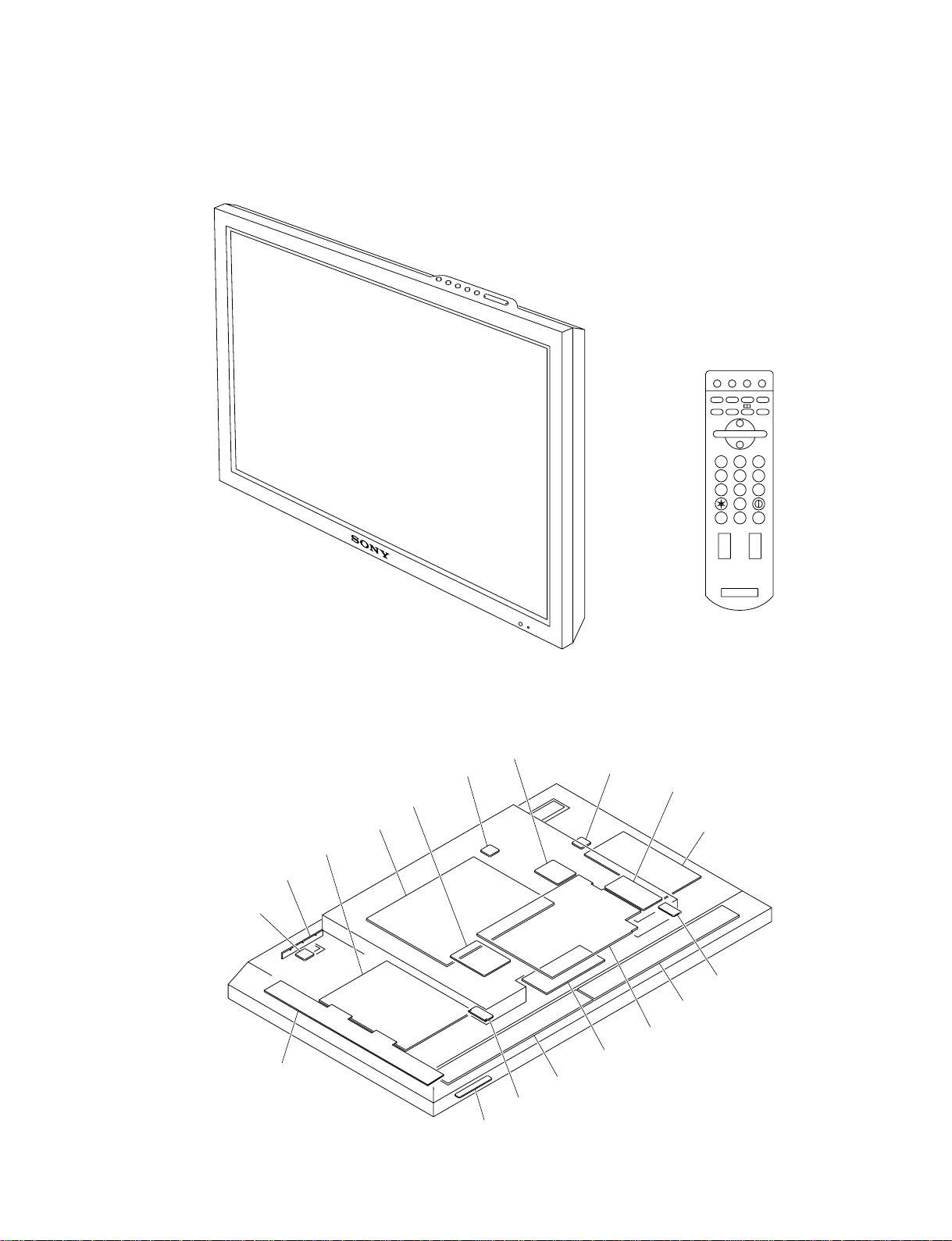
1-1. Appearance Figure
Section 1
Service Overview
1 2 3
4 5 6
7 8 9
0
ON SET OFF
1-2. Board Location
H2 board
TEMP board
Y-DRV board
Y-SUS board
G board
L board
TEMP board
H1 board
I board
TEMP board
BKM-FW10
Z-SUS board
T-L board
XR board
A board
CTRL board
XL board
T-R board
FWD-42PX2
1-1
Page 8
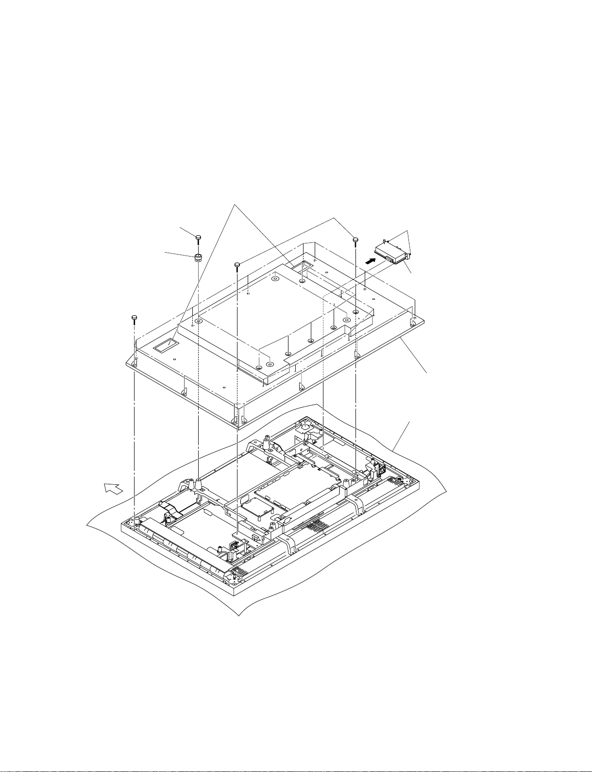
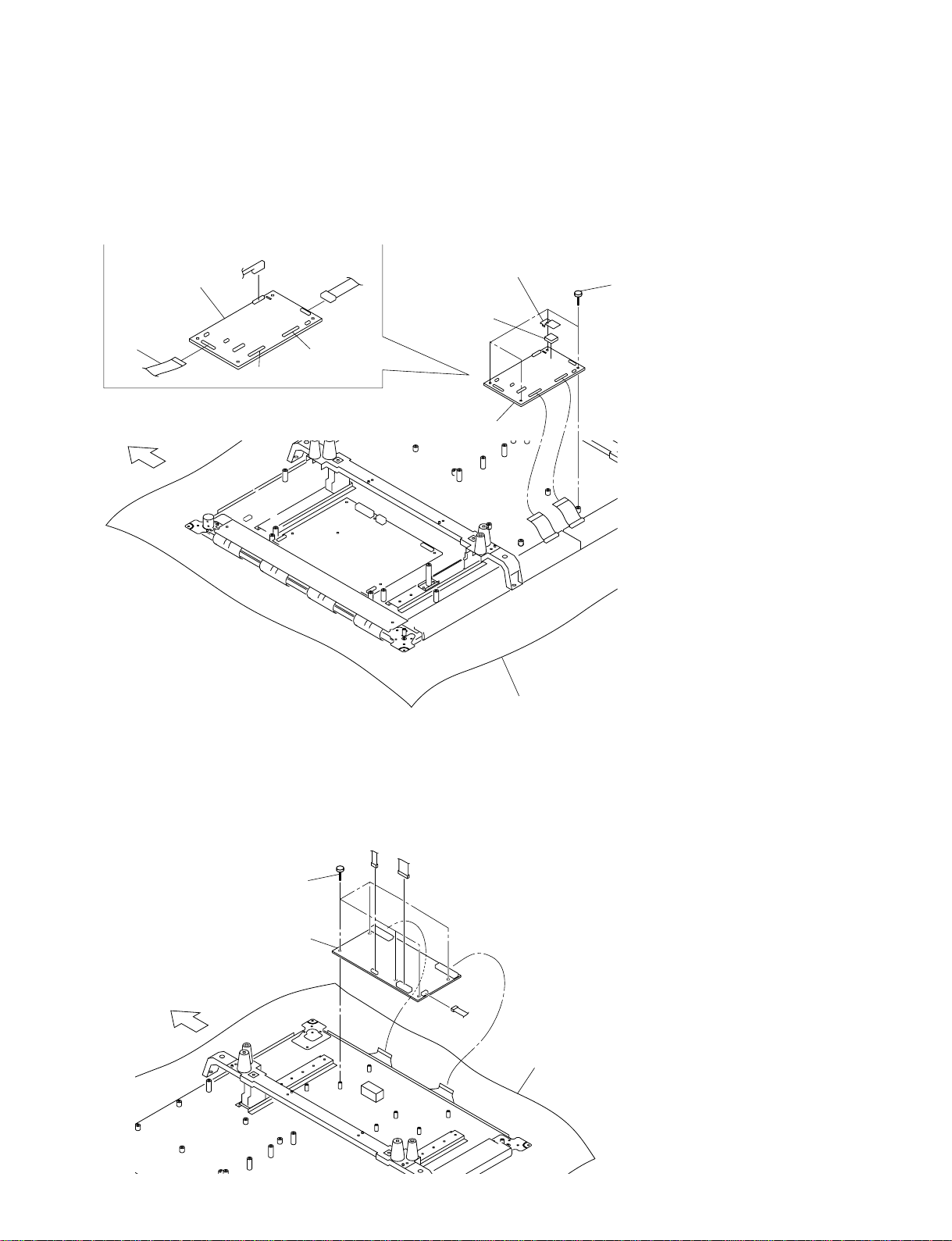
1-3. Disassembly
7
n
When removing/installing the cabinet and replacing the board, place the unit on the conductive cushion.
1-3-1. Rear Cabinet Assembly
Hold the two handles and
remove the rear cabinet assembly.
3 Four screws
6 Fourteen screws
4 Four knobs
5 Fourteen screws
1 Two panel securing
screws
2 BKM-FW10
Upper side
8 Rear cabinet assembly
Conductive cushion
1-2
FWD-42PX2
Page 9
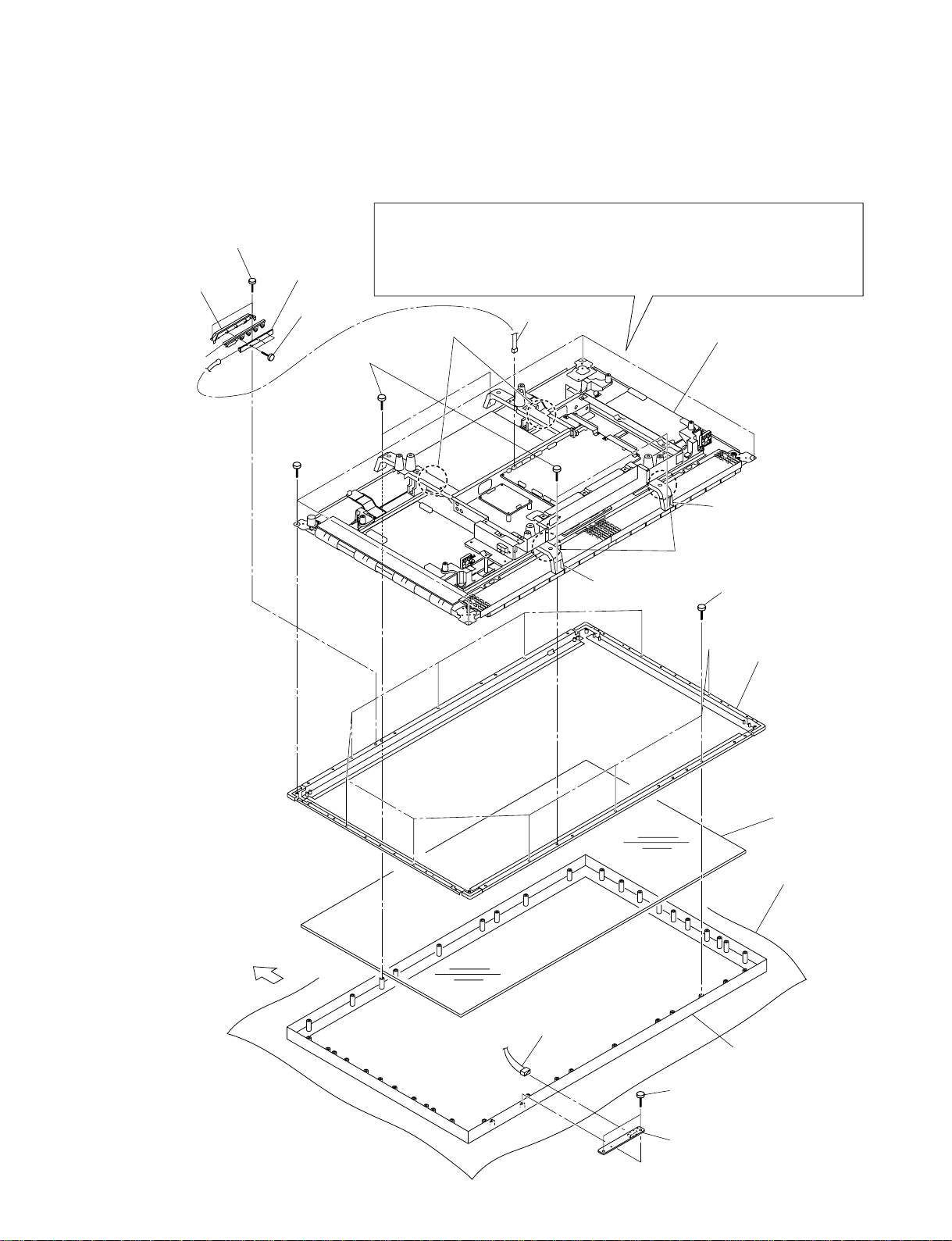
1-3-2. Bezel Assembly/H1 Board/H2 Board
. Remove the rear cabinet assembly. (Refer to Section 1-3-1.)
m
. When removing the chassis assembly, be sure to work with more than two persons.
. When removing the chassis assembly, hold the four portions A and remove it from
the front frame assembly.
. Place the removed chassis assembly on the conductive cushion.
Portions A
3 Control button
bracket
6 Control button
2 Two screws
3 H2 board
4 Three screws
1 Four screws
7 Four screws
CN3
9 Chassis assembly
Arm
Portions A
Upper side
0 Harness
Arm
8 Ten screws
![ Front frame
assembly
!= Filter glass
Conductive cushion
!- Bezel assembly
FWD-42PX2
!] Two screws
!\ H1 board
1-3
Page 10
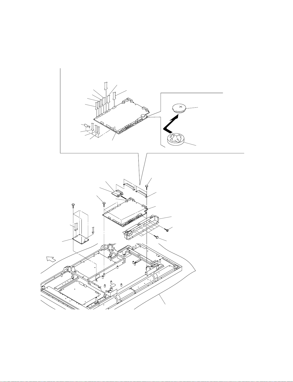
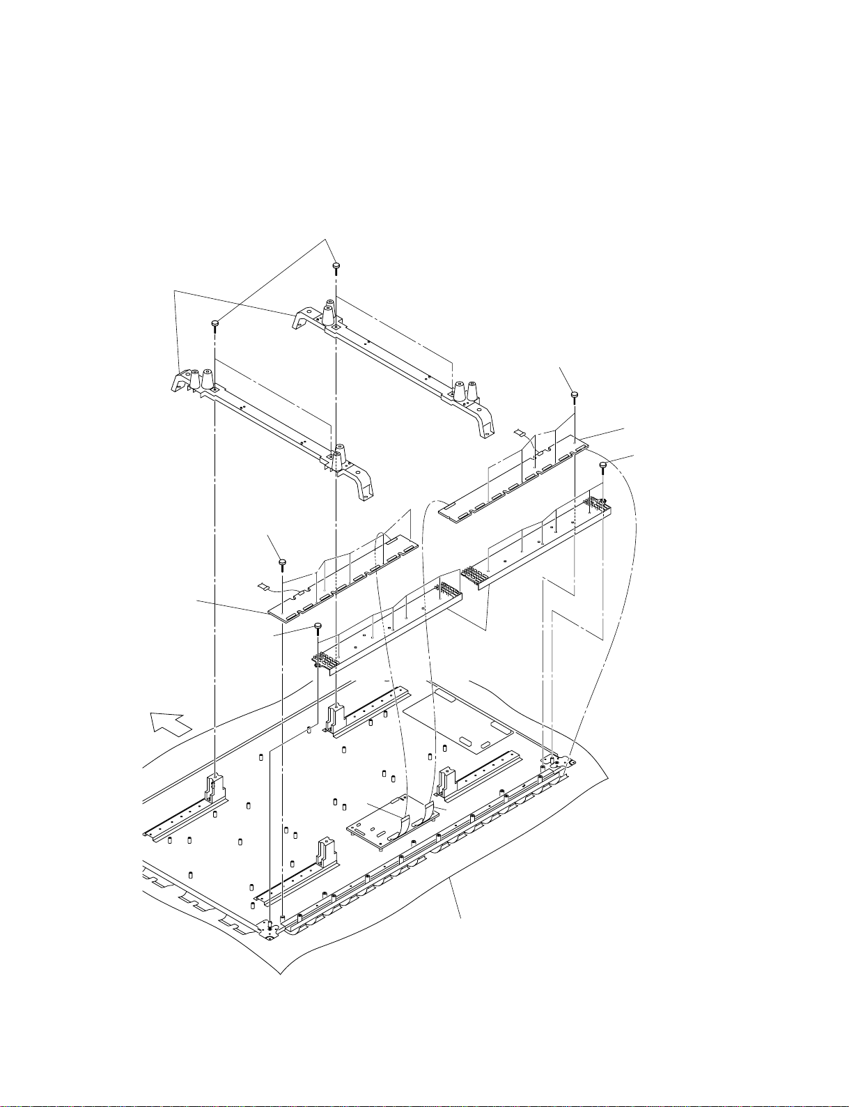
1-3-3. A Board/L Board/I Board
. Remove the rear cabinet assembly. (Refer to Section 1-3-1.)
CN24
CN29
CN3
CN22
CN501
CN9
CN8
CN23
CN19
CN15
9 A board
CN1
!= Removing the lithium battery.
Remove the lithium battery in the
direction of the arrow.
Lithium battery
(CR-2032)
Battery holder
2 L board
Upper side
8 Four screws
1 Four screws
P3
!/ I board
P1
P1
3 Four screws
4 Two screws
CN20
9 A board
7 Interface cover
5 Six connector screws
6 Screw
Conductive cushion
1-4
FWD-42PX2
Page 11
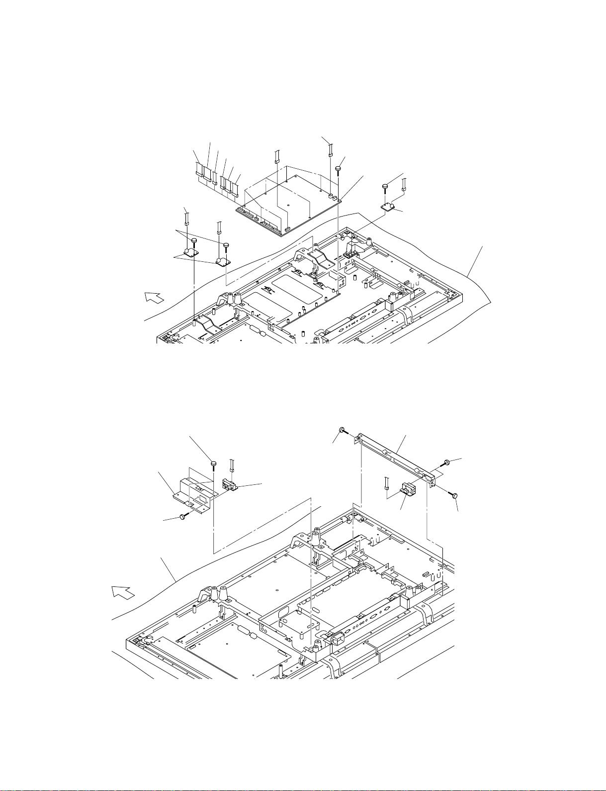
1-3-4. G Board/TEMP Board
. Remove the rear cabinet assembly. (Refer to Section 1-3-1.)
CN800
5 Two screws
6 TEMP boards
Upper side
CN807
P501
CN8
CN805
CN804
CN803
P501
CN802
CN801
1-3-5. T-R Board/T-L Board
. Remove the rear cabinet assembly. (Refer to Section 1-3-1.)
1 Eight screws
2 G board
3 Screw
P501
4 TEMP board
Conductive cushion
2 AC outlet cover
3 Two screws
Conductive cushion
Upper side
1 Three screws
CN1304
4 T-R board
5 Screw
7 Option shield plate
CN1302
9 T-L board
8 Two screws
6 Screw
FWD-42PX2
1-5
Page 12
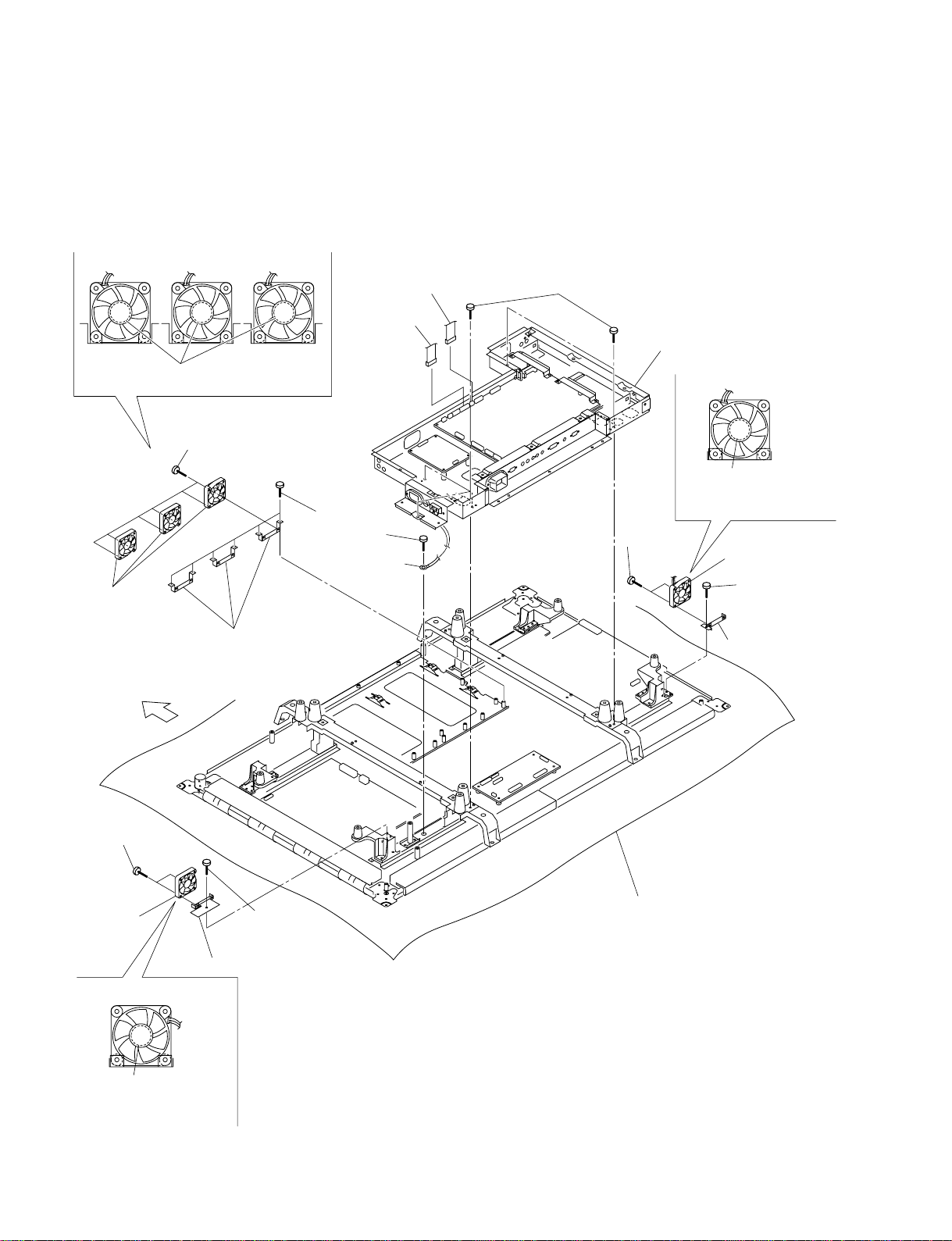
1-3-6. A Block Assembly/DC Fan
. Remove the rear cabinet assembly. (Refer to Section 1-3-1.)
. Remove the bezel assembly. (Refer to Section 1-3-2.)
. Remove the G board. (Refer to Section 1-3-4.)
DC fan installation direction
6 CN24
5 CN23
Make sure that the label is oriented in the
upward direction of the main unit.
![ Six screws
!- Six screws
2 Screw
3 Round type
connector
!] DC fans
1 Five screws
4 A block assembly
DC fan installation direction
9 Two
screws
Make sure that the label is
oriented in the upward
direction of the main unit.
0 DC fan
7 Screw
!= Fan brackets
Upper side
!' Two screws
!, DC fan
!; Fan bracket
DC fan installation direction
Make sure that the label is
oriented in the upward
direction of the main unit.
8 Fan bracket
Conductive cushion
!\ Screw
1-6
FWD-42PX2
Page 13
1-3-7. Y-DRV Board/Y-SUS Board
. Remove the rear cabinet assembly. (Refer to Section 1-3-1.)
. Remove the bezel assembly. (Refer to Section 1-3-2.)
P1
7 Y-DRV board
1 Two screws
2 Speaker bracket
support
Upper side
Conductive cushion
5 Three screws
P1
P2
P3
P4
P11
P5
P2
P6
P7
P8
P9
6 Six screws
P4
P152
P8
8 Y-SUS board
3 Two screws
4 Speaker bracket
support
FWD-42PX2
1-7
Page 14
1-3-8. CTRL Board
. Remove the rear cabinet assembly. (Refer to Section 1-3-1.)
. Remove the bezel assembly. (Refer to Section 1-3-2.)
. Remove the A block assembly. (Refer to Section 1-3-6.)
P6
4 CTRL board
P7
P10
P4
3 Cushion
P11
2 Cushion retainer
1 Four screws
Upper side
4 CTRL board
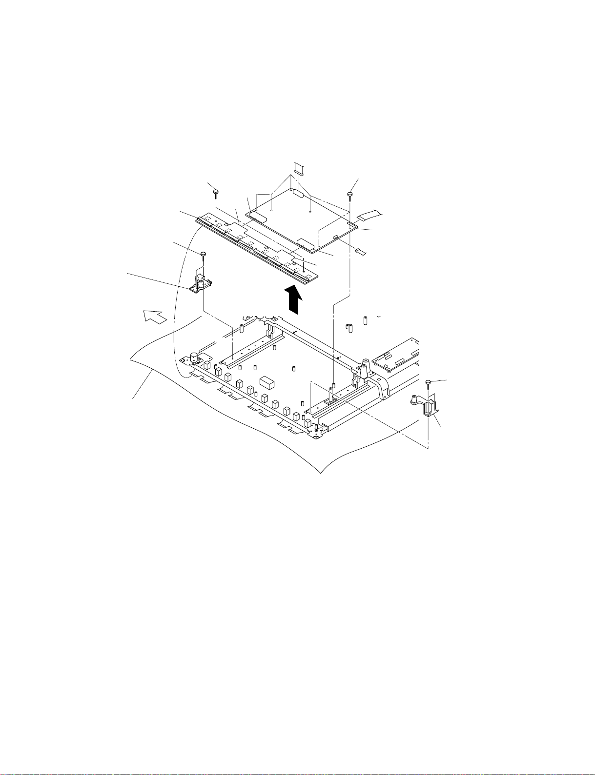
1-3-9. Z-SUS Board
. Remove the rear cabinet assembly. (Refer to Section 1-3-1.)
. Remove the bezel assembly. (Refer to Section 1-3-2.)
P2
P1
1 Five screws
Conductive cushion
1-8
Upper side
2 Z-SUS board
P4
P6
Conductive cushion
P5
FWD-42PX2
Page 15
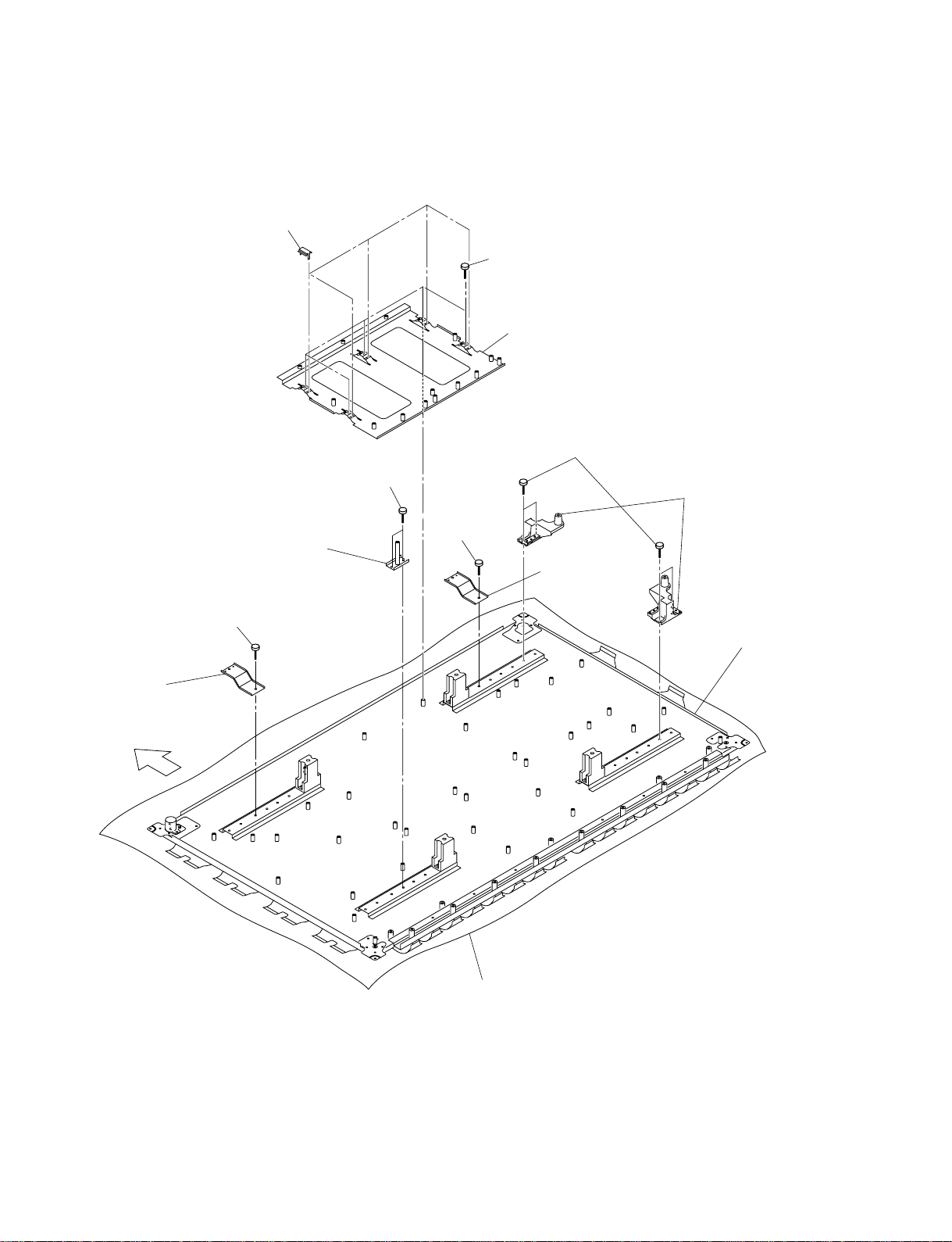
1-3-10. XL Board/XR Board
. Remove the rear cabinet assembly. (Refer to Section 1-3-1.)
. Remove the bezel assembly. (Refer to Section 1-3-2.)
. Remove the A block assembly. (Refer to Section 1-3-6.)
1 Four screws
2 Two frame modules
8 Five screws
7 XL board
Upper side
6 Six screws
P210
3 Seven
screws
P208
P207
P206
P10
P205
P204
5 Flexible retainer
P108
P201
P202
P203
Conductive cushion
P11
P107
P106
P110
P105
P104
P103
P102
9 XR board
4 Six screws
P101
FWD-42PX2
1-9
Page 16
1-3-11. Plasma Display Panel
. Remove each part. (Refer to Sections 1-3-1 to 1-3-10.)
9 Five covers
3 Two screws
4 AC socket
support
!/ Five screws
!- G board bracket
7 Four screws
8 Speaker bracket
supports
5 Screw
6 Bracket
2 Bracket
Upper side
1 Screw
!= Plasma
display
panel
Conductive cushion
1-10
FWD-42PX2
Page 17
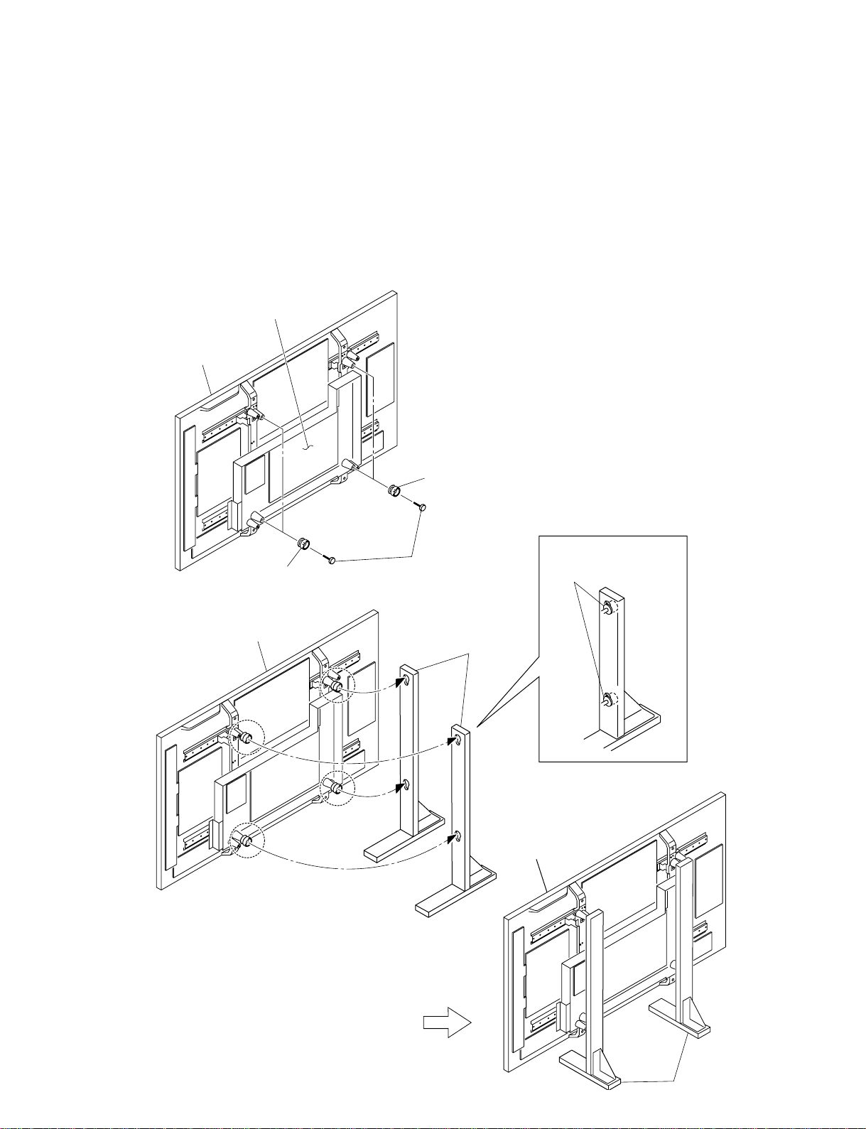
1-4. Service Position
1-4-1. Service Position of A Board
m
. When attaching this unit to the stands, be sure to work with two persons.
. After attaching this unit to the stands, make sure that the knobs are securely inserted into the holes of
the stands.
. When assembling the service position, be sure to repair after removing the rear cabinet.
A board
Unit
1 Knobs
Unit
1 Knobs
2 Four screws
Stands
Insert the four knobs into
the holes of stands.
Unit
FWD-42PX2
Stands
1-11
Page 18

1-5. Packing of the Plasma Display Panel
8 Lid of outer box
5 Protection plate for outer box
3 Inner box (front)
2 Protection plate
for inner box
Front
7 Outer box
Rear
2 Protection plate for inner box
4 Inner box (rear)
5 Protection plate
for outer box
1-12
1 PDP module
6 Palette
FWD-42PX2
Page 19

1-6. Label Information of Module
2 3 1 4 5
1 Warning/Caution label
2 Voltage label
3 Identification label
4 Safety approval label
5 Serial No. of frame
1-6-1. Warning/Caution Label
!
HIGH
VOLTAGE
1 Warning (High Voltage)
2 Warning (Hot Surface)
3 Caution (Mechanical Hazard)
WARNING
HAZARD VOLTAGE.
DO NOT TOUCH ELECTRIC POINT.
123
SURFACE
!
HOT
18.5 cm
WARNING
HOT PART CAN BE BURN.
DO NOT TOUCH ELECTRIC PART.
!
WOUND
CAUTION
MECHANICAL HAZARD.
DO NOT TOUCH POINTED PART.
2.1 cm
FWD-42PX2
1-13
Page 20

1-6-5. Serial No. of Frame Label1-6-2. Voltage Label
7 cm
MODEL : PDP42X3####
All Voltage : DC(=) 5.2V
Va : 60V Vs : 186V
150 / -200 / 120 / N.A / 100
Max Watt : 330W(Full White)
1-6-3. Identification Label
7 cm
MODEL : PDP42X30000
512K343X3001108.AKLGG CC
LG Electronics Inc.
. Model Name
. Bar Code (Contains the manufacture No.)
. Manufacture No.
. The trade name of LG Electronics
. Manufactured date (Year & Month)
. The place Origin
. Mode Suffix
Date 2005.12 Made in Korea
2.5 cm
7 cm
P/N : 3315Q-H034A
2.5 cm
W4205C014819
LG Electronics Inc.
2.5 cm
1-6-4. Safety Approval Label
7.5 cm
MODEL=PDP42X3####
Rating
Total Max Watt:340W
Max Volt(=):5.25V/65Va/195Vs
Max Amps:4.5A/2.0A/1.5A
LG Electronics Inc.
. Model Name
. Max. Watt (Full White)
. Max. Volts
. Max. Amps
. The Trade Name of LG Electronics
. TUV Approval Mark
. UL Approval Mark
. UL Approval No.
2.5 cm
1-14
FWD-42PX2
Page 21

1-7. Warning on Power Connection
Use a proper power cord for your local power supply.
The United States, Continental Europe UK, Ireland, Australia, Japan
Canada New Zealand
Plug type VM0233 COX-07/636 –
Female end VM0089 COX-02/VM0310B VM0303B VM1313
Cord type STV H05VV-F CEE (13) 53rd (O, C) HVCTF
Rated Voltage & Current 10 A/125 V 10 A/250 V 10 A/250 V 10A/125V
Safety approval UL/CSA VDE VDE DENAN-HO
1) Use an appropriate rating plug which is applied to local regulations.
1)
VM1296
1-8. Unleaded Solder
Boards requiring use of unleaded solder are printed with a lead free mark (LF) indicating the solder
contains no lead.
(Caution: Some printed circuit boards may not come printed with the lead free mark due to their
particular size.)
LEAD FREE MARK
Pb
m
. Be sure to use the unleaded solder for the printed circuit board printed with the lead free mark.
. The unleaded solder melts at a temperature about 40 dC higher than the ordinary solder, therefore, it is
recommended to use the soldering iron having a temperature regulator.
. The ordinary soldering iron can be used but the iron tip has to be applied to the solder joint for a
slightly longer time. The printed pattern (copper foil) may peel away if the heated tip is applied for too
long, so be careful.
FWD-42PX2
1-15
Page 22

Page 23

Service Mode and Adjustment
(
)
INITIALIZATION
. EEPROM INIT. . MODEL NAME
. EXCEPT WB . FILL 0xFF
. ONLY WB INIT . SERIAL MODE
. ELAPSED TIME
. SERIAL NO.
FOR TEST
. AGING ON/OFF
. FAN ON/OFF
. INIT GOODS
FOR SONY
. S-INIT GOOD
. FAN FOR TEST
. SELECT RS232 MAIN
TEMPERATURE
. REFER.SAVE . SENSOR2
. SENSOR1 . SENSOR3
WB DEFAULT DATA
. PC . DVI
. VIDEO . COPY WB DATA
. DTV
(Continued)
2-1. Service Mode
2-1-1. Service Mode Startup Procedure
1. Press the [ENTER] button of the remote controller
(RM-980).
2. Enter the number 1 → 8 → 2 in order.
2-1-2. Configuration
Section 2
ASI510-MAIN
ASI510-SUB
ADC
AD CALIBRATION
UPD64012
AUDIO
WHITE BALANCE
Continued
. CONTRAST . GAMMA-G
. BRIGHT . GAMMA-B
. SHARP-Y . NOISE
. SHARP-C . BLACK EXPD
. GAMMA-R . WHITE EXPD
. CONTRAST . GAMMA-R
. BRIGHT . GAMMA-G
. SHARP-Y . GAMMA-B
. SHARP-C
. CONTRAST-R . BRIGHT-B
. CONTRAST-G . CLOCK
. CONTRAST-B . PHASE
. BRIGHT-R . AUTO
. BRIGHT-G
. PC.CUTOFF . CONT.G
. PC.GAIN . CONT.B
. DTV.CUTOFF . BRT.R
. DTV.GAIN . BRT.G
. CONT.R . BRT.B
. CONTRAST . IFC
. BRIGHT . CBW
. SATURATION . LDLY
. HUE . YOF
. BRIGHT-CIP . ASI 0x238
. CONT-CIP . ASI 0x239
. SATUR.-CIP . ASI 0x23A
. TINT-CIP . ASI 0x23B
. DELAY
. COLOR TEMP . SUB-GAIN
. R-GAIN . SUB PK
. G-GAIN . SUB GAMMA
. B-GAIN . SUB CHROMA
. R-OFFSET . SUB SHARP
. G-OFFSET . SHARP OFFS
. B-OFFSET . I/P LTI
. SUB-OFFSET . PBPR BAL
FWD-42PX2
2-1
Page 24

2-1-3. Description of Main Items
1. AD CALIBRATION
PC.CUTOFF: Sets Cut Off of PC mode.
PC.GAIN: Sets Gain of PC mode.
DTV.CUTOFF: Not used
DTV.GAIN: Not used
CONT.R: Not used
CONT.G: Not used
CONT.B: Not used
BRT.R: Not used
BRT.G: Not used
BRT.B: Not used
2. AUDIO
DELAY: Sets delay timing of Audio sound.
(0, 5, 15, 20, .....115, 120)
3. WHITE BALANCE
COLOR TEMP: Sets color temperature (11000, 9300,
6500).
R-GAIN: Sets Red Gain (contrast).
G-GAIN: Sets Green Gain (contrast).
B-GAIN: Sets Blue Gain (contrast).
R-OFFSET: Sets Red Offset (brightness).
G-OFFSET: Sets Green Offset (brightness).
B-OFFSET: Sets Blue Offset (brightness).
SUB-OFFSET: Not used
SUB-GAIN: Not used
5. FOR TEST
AGING ON/OFF: Sets Aging Mode on/off.
FAN ON/OFF: Sets fan on/off.
INIT GOODS: Initializes whole data for user to be
able to use the set.
6. FOR SONY
S-INIT GOOD: Initializes whole data except Operation
Time for user to be able to use the set.
FAN FOR TEST: Sets fan on/off.
n
This mode is used for the check in
service. The fan is stopped under
normal condition. It operates when the
temperature inside of this unit rises.
SELECT RS232C: Not used
7. WB DEFAULT DATA
PC: Not used
VIDEO: Not used
DTV: Not used
DVI: Not used
COPY WB DATA: Not used
4. INITIALIZATION
EEPROM INIT.: Initializes EEPROM to default data.
EXCEPT WB: Initializes data except white balance.
ONLY WB INIT: Initializes white balance data only.
ELAPSED TIME: Initializes Operation Time.
SERIAL NO.: Initializes Serial Number.
MODEL NAME: Initializes Model Name.
FILL 0xFF: Initializes EEPROM to 0xFF.
SERIAL MODE: Sets Serial Mode to communicate with
the set by using RS-232C.
If INT GOODS is run, this is set to
SONY.
SONY: This is for user to control the
set by using RS-232C as
remote controller.
LG: This is for setting white
balance.
ETC: This is for developer.
2-2
RS-232C cable
COM port
Personal computer
Cable connection
FWD-42PX2
Page 25

2-2. White Balance Adjustment
2-2-1. Initialization
Initialize all information stored in EEPROM.
1. Press the [ENTER] button of the remote controller
(RM-980).
2. Enter the number 1 → 8 → 2 in order.
The service mode starts up.
3. Select INITIALIZATION menu and run FILL 0xFF.
n
When the setting is completed, the unit becomes ON
state automatically after power ON/OFF.
2-2-2. AD Calibration
Run Auto Calibration in PC (1024 x 768@60Hz) signal.
2-2-3. 1PC Signal
1. Start the service mode. (Refer to Section 2-1-1.)
2. Select AD CALIBRATION menu.
3. Input Full Black (No Video) pattern.
4. Run PC. CUTOFF.
5. Input Full White Pattern.
6. Run PC.GAIN.
2-2-4. White Balance
Signal level
700 mV p-p
Signal pattern
. 191-level (75IRE) full white pattern
. 2/16 gray (16’st step at 255 level)
Color matrix adjustment
Run the following program sequence in order PC → 1080i
→ 480p → 480i → 575i → NTSC Composite → PAL
Composite.
1. After input each signal, adjust Sub Offset.
. Input 16-Gray Pattern.
. Activate SERVICE MODE OSD and select WHITE
BALANCE menu.
. Change SUB-OFFSET and adjust Brightness of 2/16
gray level into under 0.8cd/m2.
(SUB-OFFSET: ±10)
2. Input Full White Pattern.
3. Setup R-GAIN and R/G/B-OFFSET values of the
WHITE BALANCE menu into the following TABLE
value.
PC 1080i 480p 480i 575i NTSC PAL
R Gain 33 34 34 34 34 34 34
G Gain 32 33 33 33 33 33 33
B Gain 31 32 32 32 32 32 32
R Offset 61 61 61 61 61 61 61
G Offset 60 60 60 60 60 60 60
B Offset 63 63 63 63 63 63 63
After aging the set about 30 min., adjust color matrix of
each color temperature 11000K/9300K/6500K.
Preparation for adjustment
Required equipment
. Signal generator (ex: VG-828)
. Color analyzer (ex: CA1000)
Signals
n
If want to know detail timing. Refer to Sony Timing Spec.
. PC WXGA (1024 x 768@60 Hz)
. 1080I (Y/Pb/Pr)
. 480P (Y/Pb/Pr)
. NTSC composite
. PAL composite
. 480I (NTSC component)
. 575I (PAL component)
FWD-42PX2
4. Change G-GAIN and B-GAIN values and adjust color
matrix. (Refer to Sony Color Matrix Spec.)
11000K: x = 276 (±15), y = 282 (±15)
9300K: x = 283 (±15), y = 298 (±15)
6500K: x = 313 (±15), y = 329 (±15)
5. Adjust each color temperature 11000K/9300K/6500K
in order repeating steps 3 and 4.
Shipment condition setting
Set up the shipment condition.
1. Start the on service mode.
(Refer to Section 2-1-1.)
2. After selecting FOR TEST menu, run INIT GOODS.
n
When the setting is completed, the unit becomes ON
state automatically after power ON/OFF.
2-3
Page 26

2-3. Va/Vs Voltage Adjustment
2-3-1. Required Equipment
. Digital multi meter
. Signal generator
Input signal: Input1 (RGB, D-Sub) 1024 x 768@60 Hz (Recommended pattern), 100 % white pattern
2-3-2. Vs Voltage Adjustment
1. Check the label on the right upper side of PDP panel
2. Turn the volume (1VR600) to be “Vs Voltage” on the label.
Check point: 2, 3-pins (Y board)
It is normally set in the range between 180 V and 195 V.
2-3-3. Va Voltage Adjustment
1. Look at the label on the right upper side of PDP panel
2. Then turn the volume (1VR700) to be “Va Voltage” on the label.
Check point: 10-pins (Y board)
It is normally set in the range between 55 V and 65 V.
2, 3 pins
10-pin
1VR600
1VR700
2-4
FWD-42PX2
Page 27

2-4. Vsc/
__
_Vy Voltage Adjustment
__
After replacing the Y-SUS board, perform the adjustment in this section.
2-4-1. Required Equipment
. Digital multimeter
. Signal generator
Input signal: Input1 (RGB, D-Sub) 1024 x 768@60 Hz (Recommended pattern), 100% white pattern
2-4-2. Vsc Voltage Adjustment
1. Perform the adjustment so that the following specification is satisfied.
Adjustment point: C51
Specification: See below
2-4-3.
__
_Vy Voltage Adjustment
__
1. Perform the adjustment so that the following specification is satisfied.
Adjustment point: R36
Specification: See below
_Vy specification value Vsc specification value
n
The above is a voltage label sample.
Check the actual model for the actual specification value.
V
SC
adjustment volume
VSC measuring point
_Vy adjustment volume
FWD-42PX2
GND
_Vy measuring point
2-5
Page 28

2-5. Flash Down-loading Method
Preparation
1. Connect this unit with PC using the RS-232C cable.
2. Disconnect the AC power cord of this unit.
Download
1. Start the file, “FWD42PX2_Down.exe”.
2. Select “COM1” as COM Port and “57600” as baud
rate as below picture.
3. Click the [Port|Setup], then click the [OK] button.
4. Click the [Load] button, then select the file from the
designated folder.
5. Click the [Run|DownLoad] button.
Download is started. (Down Load Time : about 5
minutes)
If down load is finished, the monitor will be re-booted
automatically.
m
. Do not remove AC cord from PC and monitor while
down load operation is being proceeded.
. After processing micom update with ISP program,
please execute following in order for the unit to
maintain “Shipping default condition”.
* Execute EXCEPT WB in INITIALIZATION.
* Execute COPY WB DATA in WB DEFAULT
DATA.
* Execute INIT GOODS in FOR TEST.
2-6
FWD-42PX2
Page 29

2-6. DEVICEINFO Section
1. Connect PC to PDP using the serial cable.
2. Set the port.
(1) Select the model. (FWD-42PX2)
(2) Select the port. (COM1, COM2, COM3 or COM4)
n
The initial setting is COM1.
3. Click the [Read] button in “Model Name”.
(Data reading)
If the data reading is completed successfully, the
setting in the port that has been selected in step 2 can
be performed. If not, return to step 2 and select another
port. Then, perform the data reading again.
4. Data writing
Modify: Model name, serial number, operating time
Write: Model name, serial number, operating time
FWD-42PX2
2-7
Page 30

Page 31

Section 3
Troubleshooting
3-1. Self Diagnosis Operation
Check Items Status
Panel Communication error Power Off → LED Blinking 2 times
FAN Abnormal Power On → LED Blinking 3 times
Temp. Abnormal Power Off → LED Blinking 4 times
Voltage Abnormal
*: There is abnormal state in any of 5 V/9 V/3.3 V/Vs/Va/12V that is output from the G board.
3-2. Check Point
3-2-1. A Board
*
Power Off → LED Blinking 5 times
LED symptoms
1. No LED flashing
Cause 1: G board can’t supply 5 V.
(Check 3 and 4-pins of the CN9 on the A
board.)
→ Check the connector, or replace the G board.
Cause 2: Pattern on the A board is short.
→ Replace the A board or H1 board.
2. Only red LED lighting (No power on)
Cause 1: Check the 5 V line from the G board to the A
board.
(Check 1-pin of the CN9 on the A board.)
→If the 5 V line is abnormal, check the
connector, or replace the G board. If it is ok,
replace the A board.
Cause 2: Micom halt
→ Replace the A board.
3. Only amber LED lighting (No power on)
Cause 1: Micom halt → Replace the A board.
4. Repeated blinking from red to green LED
flashing (No power on)
Cause 1: A board is damaged.
→ Replace the A board.
Cause 2: G board can’t supply another voltage.
→ Replace the G board.
Raster symptoms (If LED is ok)
1. No raster
(First check back raster if plasma display
panel is on)
Cause 1: If it is ok, replace the A board.
Cause 2: If it is not, replace the G board or plasma
display panel.
2. No raster at special mode.
Cause 1: Replace the A board.
Cause 2: If there is no raster after inputting the DVI
signal, check EDID.
3. Abnormal raster
Cause 1: When you change A board, it is abnormal.
→ Plasma display panel has problem.
Sound Symptoms
1. You can’t hear sound output
Cause 1: Check 1 and 3-pins of the CN1 on the L board. If
it is ok, replace the L board.
The 3-pin of CN1 is the L/R output terminal of
the audio signal. Check the signal using the
oscilloscope. If there is no signal, the A board is
the cause of the trouble. Otherwise, the L board
is the cause of the trouble.
Cause 2: If it is not, replace the A board.
5. Blinking red LED many times.
Refer to Section 3-1.
FWD-42PX2
2. Abnormal sound
Cause 1: Replace the L board.
3-1
Page 32

3-2-2. Plasma Display Panel
1. Image is not displayed.
. Check all connectors.
. Check the Exhaust tip.
. Check blink of LEDs on the CTRL board and check the
5 V CTRL voltage.
. Check fuse on the Y-SUS board and check Vsc, _Vy,
Vs, V5 CTRL voltage.
. Check fuse on the Z-SUS board and check Va, V5
CTRL, Vs voltage.
2. Vertical bar failure
. Check all connectors.
. Check peripheral circuit and connecting of the XR and
XL boards.
4. Mal discharge
. Check signals of Y-DRV and Z-SUS boards and check
Y-SUS board voltage (_Vy, Vsc).
. Check Y-DRV board.
. Check CTRL board.
3. Horizontal bar failure
. Check all connectors.
. Check peripheral circuit and connecting of the Y-DRV
board.
3-2
FWD-42PX2
Page 33

3-3. Image Trouble
Main symptoms
. Dot noise . Picture noise . Bad color . Vertical dot noise . Unstable image
. No image . Broken OSD . No inversion . No power saving . Clock error
. No screen saver . Flashing picture . Dark picture . Unstable caption/text
Image is abnormal.
Are all input signals abnormal?
(RGB/DVI/YUV/CVBS)
Yes
Is the connection of the A board
abnormal?
. Image is not correctly displayed.
. Power goes off.
No
Is the G board abnormal?
. Image is dark or flashing.
. Power cannot be turned on,
or setting is reset.
No
n
For the replacement parts, refer to Section 4.
The parts other than those described in Section 4 are
not service parts. When the replacement of those parts
is required, replace them in the assembly unit.
No
Yes
Yes
There is a high possibility that
the A board caused the trouble.
→ Replace the A board.
Connect correctly. If the trouble
persists, replace the A board.
Perform Va and Vs voltage adjustments.
(Refer to Section 2-3.)
If the trouble persists, replace the
G board.
n
After replacing the A board, perform the following
adjustments.
. AD calibration adjustment (Refer to Section 2.)
. White balance adjustment (Refer to Section 2.)
. EDID data input
. S-init Goods (Refer to Section 2.)
n
After replacing the A board, perform the following
adjustments.
. AD calibration adjustment (Refer to Section 2.)
. White balance adjustment (Refer to Section 2.)
. EDID data input
. S-init Goods (Refer to Section 2.)
n
After replacing the G board, perform
the following adjustments.
. Va Voltage Adjustment (Refer to Section 2-3.)
. Vs Voltage Adjustment (Refer to Section 2-3.)
Is the CTRL board abnormal?
(Refer to Sections 3-3-2 and
3-8.)
No
Is the Y-SUS board abnormal?
(Refer to Sections 3-3-2 and
3-8.)
No
Replace the Z-SUS board.
FWD-42PX2
Yes
Yes
Replace the CTRL board.
Replace the Y-SUS board.
n
After replacing the Y-SUS board, perform
the following adjustments.
. Vsc Adjustment (Refer to Section 2-4.)
._Vy Adjustment (Refer to Section 2-4.)
3-3
Page 34

3-4. Power (G Board) Trouble
Power cannot be turned on.
Is there any trouble in AC power
cable or line filter cable?
No
Is LED reset repeatedly?
No
Is there any abnormal state in
the connection between the
G board and A board.
No
n
For the replacement parts, refer to Section 4.
The parts other than those described in Section 4 are
not service parts. When the replacement of those parts
is required, replace them in the assembly unit.
Yes
Yes
Yes
Identify the trouble portion and
improve it.
There is a high possibility that
the A board caused the trouble.
→ Replace the A board.
Connect correctly.
n
After replacing the A board, perform the following
adjustments.
. AD calibration adjustment (Refer to Section 2.)
. White balance adjustment (Refer to Section 2.)
. EDID data input
. S-init Goods (Refer to Section 2.)
Is the G board abnormal? (*)
No
Is the A board abnormal?
. Check where is short pattern.
. Re-on (2-pin of CN9 on the
A board): High 1 V.
. Vs-on (7-pin of CN9 on the
A board): High 1 V.
No
Replace the CTRL board.
(*)
. 5 Vst (Stand by 5 V, 3, 4-pins of CN9 on the A board): 5 V
. AC-DET (1-pin of CN9 on the A board): 5 V
. Re-on (Rely-on switching signal, pin-2 of CN9 on the A board): High 1 V
. Vs-on (Vs-on signal, pin-7 of CN9 on the A board): High 1 V
Yes
Yes
Replace the G board.
Replace the A board.
n
After replacing the G board, perform
the following adjustments.
. Va Voltage Adjustment (Refer to Section 2-3.)
. Vs Voltage Adjustment (Refer to Section 2-3.)
n
After replacing the A board, perform the following
adjustments.
. AD calibration adjustment (Refer to Section 2.)
. White balance adjustment (Refer to Section 2.)
. EDID data input
. S-init Goods (Refer to Section 2.)
3-4
FWD-42PX2
Page 35

3-5. Remote Control Trouble
Remote control is abnormal.
Is there any abnormal state in
the connection between CN22
on the A board and CN1 on the
H1 board?
No
Is the H1 board abnormal?
No
Replace the A board.
n
For the replacement parts, refer to Section 4.
The parts other than those described in Section 4 are
not service parts. When the replacement of those parts
is required, replace them in the assembly unit.
Yes
Yes
n
After replacing the A board, perform the following
adjustments.
. AD calibration adjustment (Refer to Section 2.)
. White balance adjustment (Refer to Section 2.)
. EDID data input
. S-init Goods (Refer to Section 2.)
Connect correctly.
Replace the H1 board.
3-6. Sound Trouble
Sound is abnormal.
Is there any abnormal state
in the following items?
. P1 and P3 on the L board
. CN1 on the A board
. CN1302 on the T-L board
. CN1304 on the T-R board
No
Is the L board abnormal?
. Check 1 to 4-pins of P3.
No
Replace the A board.
FWD-42PX2
n
For the replacement parts, refer to Section 4.
The parts other than those described in Section 4 are
not service parts. When the replacement of those parts
is required, replace them in the assembly unit.
Yes
Yes
n
After replacing the A board, perform the following
adjustments.
. AD calibration adjustment (Refer to Section 2.)
. White balance adjustment (Refer to Section 2.)
. EDID data input
. S-init Goods (Refer to Section 2.)
Replace the defective parts.
Replace the L board.
3-5
Page 36

3-7. Other Trouble
(
)
Button failure
Is there any abnormal state in
the connection between CN3
on the A board and the H2 board?
No
Is there any abnormal state in
the following items?
. Resistance of the H1 board
. R12 on the A board (*)
No
Replace the A board.
n
For the replacement parts, refer to Section 4.
The parts other than those described in Section 4 are
not service parts. When the replacement of those parts
is required, replace them in the assembly unit.
Yes
Yes
n
After replacing the A board, perform the following
adjustments.
. AD calibration adjustment (Refer to Section 2.)
. White balance adjustment (Refer to Section 2.)
. EDID data input
. S-init Goods (Refer to Section 2.)
Connect correctly. (*)
Replace the defective parts.
Feedback voltage (in the normal state)
Check R12 voltage while pressing each button.
. DC POWER: 0.07 V
. ENTER: 0.38 V
. UP: 0.85 V
. DOWN: 1.23 V
. MENU: 1.61 V
. INPUT: 2.05 V
. NO KEY: 3 V
DC fan operation failure
Is there any abnormal state
in the connection CN23 and
CN24 on the A board.?
No
Is there any abnormal state in
the following items of the fan
assembly? (*)
. 1 to 8-pins of CN23
. 1, 2-pins of CN24
No
Replace the A board.
n
For the replacement parts, refer to Section 4.
The parts other than those described in Section 4 are
not service parts. When the replacement of those parts
is required, replace them in the assembly unit.
Yes
Yes
n
After replacing the A board, perform the following
adjustments.
. AD calibration adjustment (Refer to Section 2.)
. White balance adjustment (Refer to Section 2.)
. EDID data input
. S-init Goods
Connect correctly.
Replace the DC fan.
Refer to Section 2.
(*)
In the normal state
. 1 to 8-pins of CN23: 9 V
. 1, 2-pins of CN24: 9 V
3-6
FWD-42PX2
Page 37

3-8. Plasma Display Panel
Image is not displayed.
Yes
No
Connect correctly.
Is there any abnormal state in the
connection of each board?
(Refer to “Disassembly” in
Section 1-3.)
Yes
Is there any abnormal state in
fuse?
. Y-SUS board (3 positions)
. Z-SUS board (2 positions)
No
Replace the defective fuse or the
Y-SUS board.
Perform the Va and Vs voltage
adjustments. If trouble persists,
replace the G board.
Yes
Is there any abnormal state in
the output (Va, VS and 5V) of
the G board?
. CN807 (From the G board to
the Z-SUS board)
. CN8 (From the G board to
the Y -SUS board)
No
Is there any abnormal state in
the TIP tube?
Replace the plasma display panel.
Replace the plasma display panel.
n
For the replacement parts, refer to Section 4.
The parts other than those described in Section 4 are
not service parts. When the replacement of those parts
is required, replace them in the assembly unit.
No
No
Yes
Is the symptom improved after
replacing with another Y-SUS
board?
Replace the Y-SUS board.
Yes
Yes
Is the symptom improved after
replacing with another Z-SUS
board?
Replace the Z-SUS board.
No
Yes
Is the symptom improved after
replacing with another CTRL
board?
Replace the CTRL board.
No
n
After replacing the Y-SUS board, perform
the following adjustments.
. Vsc Adjustment (Refer to Section 2-4.)
._Vy Adjustment (Refer to Section 2-4.)
n
After replacing the Y-SUS board, perform
the following adjustments.
. Vsc Adjustment (Refer to Section 2-4.)
._Vy Adjustment (Refer to Section 2-4.)
n
After replacing the plasma display panel, perform
the following adjustments.
. Va Voltage Adjustment (Refer to Section 2-3.)
. Vs Voltage Adjustment (Refer to Section 2-3.)
. AD calibration adjustment (Refer to Section 2.)
. White balance adjustment (Refer to Section 2.)
n
After replacing the plasma display panel, perform the following adjustments.
. Va Voltage Adjustment (Refer to Section 2-3.)
. Vs Voltage Adjustment (Refer to Section 2-3.)
. AD calibration adjustment (Refer to Section 2.)
. White balance adjustment (Refer to Section 2.)
n
After replacing the G board, perform
the following adjustments.
. Va Voltage Adjustment (Refer to Section 2-3.)
. Vs Voltage Adjustment (Refer to Section 2-3.)
3-8-1. Image is not displayed
FWD-42PX2
3-7
Page 38

3-8-2. Vertical Image is abnormal
Vertical image is abnormal.
Is there a symptom that the
image on the right or left half of
the screen is not displayed?
(Vertical streaks on the half
side of the screen)
No
Is there any vertical line
(line or stripe) on the screen?
Yes
Is there any abnormal state or
foreign substance in the
connection between the XR board
or XL board and the TCP
connector (on the panel) of the
trouble position?
n
For the replacement parts, refer to Section 4.
The parts other than those described in Section 4 are
not service parts. When the replacement of those parts
is required, replace them in the assembly unit.
Is there any problem in the connection
Yes
No
Yes
of the XR board or XL board?
XL board: Connection between Y-SUS
board and CTRL board
XR board: Connection between Z-SUS
board and CTRL board
No
Replace the XL or XR board.
Is there any vertical line over the
whole screen area at regular intervals?
Connect correctly or remove the
foreign substance.
Yes
Yes
Connect correctly.
Replace the CTRL board.
No
Replace the plasma display
panel.
n
After replacing the plasma display panel, perform
the following adjustments.
. Va Voltage Adjustment (Refer to Section 2-3.)
. Vs Voltage Adjustment (Refer to Section 2-3.)
. AD calibration adjustment (Refer to Section 2.)
. White balance adjustment (Refer to Section 2.)
3-8
FWD-42PX2
Page 39

3-8-3. Horizontal Image is abnormal
Horizontal image is abnormal.
Is there any abnormal state or
foreign substance in the
connection between the Y-DRV
board and the flexible flat cable
of the trouble position?
No
Is the symptom improved after
replacing with another Y-DRV
board?
No
Replace the plasma display
panel.
n
For the replacement parts, refer to Section 4.
The parts other than those described in Section 4 are
not service parts. When the replacement of those parts
is required, replace them in the assembly unit.
Yes
Yes
n
After replacing the plasma display panel, perform
the following adjustments.
. Va Voltage Adjustment (Refer to Section 2-3.)
. Vs Voltage Adjustment (Refer to Section 2-3.)
. AD calibration adjustment (Refer to Section 2.)
. White balance adjustment (Refer to Section 2.)
Connect correctly or remove the
foreign substance.
Replace the Y-DRV board.
3-8-4. Mal Discharge
Mal discharge
Replace the Y-DR V, Y-SUS,
or CTRL board.
n
For the replacement parts, refer to Section 4.
The parts other than those described in Section 4 are
not service parts. When the replacement of those parts
is required, replace them in the assembly unit.
n
After replacing the Y-SUS board, perform
the following adjustments.
. Vsc Adjustment (Refer to Section 2-4.)
._Vy Adjustment (Refer to Section 2-4.)
FWD-42PX2
3-9
Page 40

Page 41

4-1. Notes on Repair Parts
1. Safety Related Components Warning
w
Components marked ! are critical to safe operation.
Therefore, specified parts should be used in the case of
replacement.
2. Standardization of Parts
Some repair parts supplied by Sony differ from those
used for the unit. These are because of parts commonality and improvement.
Parts list has the present standardized repair parts.
3. Stock of Parts
Parts marked with “o” at SP (Supply Code) column of
the spare parts list may not be stocked. Therefore, the
delivery date will be delayed.
Section 4
Spare Parts
4. Harness
Harnesses with no part number are not registered as
spare parts.
FWD-42PX2
4-1
Page 42

Screw Kit
4-2. Exploded Views
21
4
10
6
5
2
11
13
15
15
2 4
10
13
9
1
15
2
2
3
1
15
10
2
15
6
6
15
7
8
2
3
c
15
7
13
15
15
4
13
15
2
10
7
12
b
10
7
24
1
2
8
a
14
6
8
2
1
3
16
16
16
22
16 16 16 16
17
17
18 181818
16
17
161616
16
16
16
4-2
FWD-42PX2
Page 43

19 20
Screw Kit
23
Note : The screws can be ordered in units of screw kit. (Sony part No. 21 to 23)
No. Part No. SP Description
21 X-2055-059-1 s SCREW KIT (INSIDE)
OUTSIDE SCREW KIT
!; 1SZZTYT003B
!' 1SZZTMF016B
!, 1SZZTMP010B
. The numbers encircled by round corresponds to numbers in illustrations.
No. Part No. SP Description
22 X-2055-060-1 s SCREW KIT (OUTSIDE)
WALL MOUNT SCREW KIT
!. 1WZZTKK004B
@/ 1SZZTMH006B
No. Part No. SP Description
23 X-2022-847-1 s SCREW KIT, WALL MOUNT
INSIDE SCREW KIT
1 1SZZTMP007D
2 332-102L
3 1SZZTYT001D
4 332-122E
5 339-006B
6 339-008N
7 339-008P
8 1SZZTMF016B
9 1SZZTYT016D
0 339-009F
!- 332-095L
!= 1SZZTMF012A
![ 1SZZTMP005C
!] 1SZZTMP009B
!\ 332-008M
a 1NHB0302120
b 1WZZTKK005B
c 1SZZTMH005B
FWD-42PX2
4-3
Page 44

Cover
BKM-FW10
103
108
107
104
102
No. Part No. SP Description
101 X-2024-229-1 s ASSY,FRONT FRAME
102 X-2109-622-1 s BEZEL ASSY(SILVER)
X-2109-625-1 s BEZEL ASSY(BLACK)
103 X-2109-623-1 s REAR CABINET ASSY
104 1-789-198-11 s MOUNTED CIRCUIT BOARD, H2
105 1-789-199-11 s MOUNTED CIRCUIT BOARD, H1
101
106
105
106 2-159-847-01 s GLASS, FILTER
107 2-591-335-01 s BUTTON, CONTROL
108 2-591-336-01 s BRACKET, CONTROL BUTTON
4-4
FWD-42PX2
Page 45

207
204
206
211
201
Chassis
205
209
210
208
202
203
No. Part No. SP Description
201 ! 1-417-398-21 s AC INLET
202 ! 1-787-338-11 s DC FAN
203 ! 1-787-338-21 s DC FAN
204 1-789-200-11 s MOUNTED CIRCUIT BOARD, L
205 1-789-550-11 s MOUNTED CIRCUIT BOARD, A
206 1-789-553-11 s MOUNTED CIRCUIT BOARD, I
207 1-789-564-11 s MOUNTED CIRCUIT BOARD, T-R
208 1-789-565-11 s MOUNTED CIRCUIT BOARD, T-L
209 2-681-504-01 s COVER, INTERFACE
210 2-990-241-02 s HOLDER (A), PLUG
211 ! 1-528-174-11 s LITHIUM BATTERY(CR2032)
FWD-42PX2
4-5
Page 46

Panel
301
305
FS2
303
FS3
308
F100
FS1
301
302
310
FS2
304
309
302
306
No. Part No. SP Description
301 X-2109-653-1 o MODULE FLAME ASSY
302 1-789-203-11 s MOUNTED CIRCUIT BOARD, TEMP
No. Part No. SP Description
G BOARD
F100 ! 1-576-300-51 s FUSE (POWER BOARD) 8A/250V
303 ! 1-789-551-11 s MOUNTED CIRCUIT BOARD, G
304 1-789-554-11 s MOUNTED CIRCUIT BOARD, Z-SUS
305 1-789-555-11 s MOUNTED CIRCUIT BOARD, Y-SUS
Z-SUS BOARD
FS1 ! 1-576-231-51 s FUSE (Z SUS) 4A/250V
FS2 ! 1-576-231-51 s FUSE (Z SUS) 4A/250V
306 1-789-556-11 s MOUNTED CIRCUIT BOARD, XR
307 1-789-557-11 s MOUNTED CIRCUIT BOARD, XL
308 1-789-558-11 s MOUNTED CIRCUIT BOARD, CTRL
309 1-789-559-11 s MOUNTED CIRCUIT BOARD, Y-DRV
Y-SUS BOARD
FS2 ! 1-576-231-51 s FUSE (Y SUS) 4A/250V
FS3 ! 1-576-231-51 s FUSE (Y SUS) 4A/250V
310 1-802-143-11 s PLASMA DISPLAY PANEL
307
4-6
FWD-42PX2
Page 47

406
Packing
417
408
414
412
401
409
405
410
402
411
407
404
403
415
416
406
413
No. Part No. SP Description
401 1-478-991-13 s REMOTE COMMANDER (RM-980)
402 9-885-014-97 s BATTERY COVER (FOR RM-980)
403 1-566-316-11 s CONNECTOR, CONVERSION
404 1-827-782-11 s CABLE, DVI
405 1-830-999-11 s VIDEO CABLE
406 2-591-343-01 s CUSHION (TOP & BOTTOM)
407 2-680-266-02 s MANUAL, INSTRUCTION
(JAPANESE, ENGLISH, FRENCH,
GERMAN, SPANISH, ITALIAN,
SIMPLIFIED CHINESE)
408 2-681-507-01 s INDIVIDUAL CARTON
409 2-990-242-01 s HOLDER (B), PLUG
410 3-613-640-01 o PLUG,HOLDER C
411 3-674-673-01 o STOPPER (A)
412 4-101-214-01 s HOLDER, CABLE
413 4-101-219-01 s TRAY, BOTTOM
414 4-101-222-01 s CARTON, INSIDE
415 4-101-223-01 s BAG, PROTECTION
416 4-101-224-01 o ACCESSORY BOX
417 ! ------------ CORD, POWER
(See Sec.1-6. Warning on Power Connection)
FWD-42PX2
4-7
Page 48

Overall
SS-SP42FW (Option)
BVTP
4 x 12
PSW
4 x 12
BVTP
4 x 12
PSW
4 x 12
BVTP
4 x 12
501
No. Part No. SP Description
501 A-1081-102-A s SPEAKER ASSY (42R) (RP)
(FOR SS-SP42FW/S (SILVER))
A-1083-765-A s SPEAKER ASSY (42R) (RP) WHITE
(FOR SS-SP42FW/W (PEARL WHITE))
502 A-1081-103-A s SPEAKER ASSY (42L) (RP) SILVER
(FOR SS-SP42FW/S (SILVER))
A-1083-766-A s SPEAKER ASSY (42L) (RP) WHITE
(FOR SS-SP42FW/W (PEARL WHITE))
BVTP
4 x 12
502
7-682-963-09 s SCREW +PSW 4X12(EP-FE/ZNBK/CM2)
7-685-661-14 s SCREW +BVTP4X12(EP-FE/CU,NI,CR)
4-8
FWD-42PX2
Page 49

TOP SIDE
Board Connections
CN1101
TEMP
Board
Y-SUS Board
Y-DRV Board
CN1201
H1 Board
P152
FAN4
P210
P501
H2 Board
P1
P8
3
11
9
XL Board
2
10
L Board
T-R Board
P3
P1
12
CN807
CN8
CN805
CN804
CN803
CN801
1
CN802
7
FAN1 FAN2
CN3
CN22
CN19
CN23
CN501
CN9
CN8
CN15
P7
P10
P200 P100
4
P16
P11
FAN3
CN24
CN29
A Board
CTRL Board
P4
TEMP Board
I Board
CN1
8
P501
5
T-L Board
XR Board
TEMP BoardG Board
P501
6
FAN5
P110
P4
P2
Z-SUS Board
P1
P5
P6
No. Part No. SP Description
1
1-910-002-76 o CONNECTOR ASSY, 12P MAIN
2
1-910-002-77 o CONNECTOR ASSY, 7P MAIN
3
1-910-002-81 o CONNECTOR ASSY, 4P KEY
4
1-910-002-85 s CONNECTOR ASSY, LVDS
5
1-910-002-86 o CONNECTOR ASSY, 9P SENS
6
1-910-012-52 o CONNECTOR ASSY Z SUS 8P
7
1-910-012-55 o CONNECTOR ASSY MAIN 8P
8
1-910-012-56 o CONNECTOR ASSY AU 12P
9
1-910-012-57 o CONNECTOR ASSY RMT 8P
0
1-910-013-70 o CONNECTOR ASSY MAIN 10P
!-
1-910-025-66 o CONNECTOR ASSY Y SUS 9P
!=
1-910-025-67 o CONNECTOR ASSY AUDIO 4P
. The numbers encircled by round corresponds to those
of the left illustration.
FWD-42PX2
4-9
Page 50

Page 51

Section 5
Block Diagram
5-1. Circuit Description
1. Input signal selection circuit
RGB and component signals are input to AD
converters IC88 and IC89 for selection. Video and
audio signals are switched using IC41.
2. A/D converter
This A/D converter consists of IC88 and IC89, and
their peripheral circuits. IC88 and IC89 have
preamplifier and PLL functions as well as an A/D
converter function. The RGB and component signals
from a D-Sub connector are input to the RGB signal
pins of IC88 and IC89. After the input signals are
amplified, they are converted into an 8-bit digital
signal and output to IC14. IC88 also generates a clock
of IC14.
3. Microcomputer and DDC
This microcomputer and DDC consist of IC91, OTP
memory (IC33), I/O controllers (IC2, IC8, IC36, and
IC65), and EEPROM (IC1, IC34, and IC49). IC91
controls the peripheral device using an IIC line. The
major functions are as follows:
1) Memorizes the setting value of a user in IC1.
2) Memorizes EDID data in IC34 and IC49.
6. Audio decoder (digital audio processor)
circuit
This audio decoder circuit consists of IC5 and its
peripheral circuit. IC91 controls this circuit using an
IIC line. An audio signal is digital-processed using
this circuit and output to audio amplifier IC7.
7. Deinterlace block
This deinterlace block consists of IC10 and its
peripheral circuit. IC91 controls this deinterlace block
using an IIC line. IC10 deinterlace- converts an 8-bit
digital interlace YUV signal. The converted signal is
output as a 16-bit digital YUV signal.
8. Panel link circuit
LVDS transmitter IC44 outputs the signal from IC14
to the panel using LVDS. The output signal is
converted into the former signal using the LVDS
receiver on the panel. (Same as for the output of IC14.)
9. Closed caption
The closed caption signal from IC9 is input to IC59
and mixed with a video signal.
4. Video decoder and three-dimensional comb
filter circuit
This video decoder and three-dimensional comb filter
circuit consist of IC59 and IC91 that controls the IIC
line of IC59. CVBS, Y/C, and Y/Pb/Pr signals are
converted into an 8-bit interlace signal using IC59 and
output to the deinterlace block. IC59 adjusts the
contrast, brightness, sharpness, hue, and color density.
The CVBS signal is separated into Y and C signals.
For an NTSC signal, a three-dimensional comb filter is
used.
5. DVT circuit
This DVT circuit consists of IC88 and IC89, and their
peripheral circuits. It processes a component signal of
up to DTV (729P and 1080i). This circuit is controlled
in an IIC line using IC91. It converts the component
signal from a D-Sub connector (CN10) and options 1
and 2 into a digital signal and outputs it to IC14.
FWD-42PX2
5-1
Page 52

16Bits
CCIR601
IC26, IC27
IC55, IC90
IC44
IC10
IC29
IC58
IC14
IC59
IC9
IC41
IC5IC2 IC7
IC34, IC49
IC33
IC92
IC91
24Bits
16Bits
DVI
RGB
COMPOSITE, Y/C
TMDS+HDCP
DVI/1080P/RGB (48Bit)
DVI/
~
1080i
24Bit
24Bits
Panel
YUV (PAP,
~
1080I)
DVI IIC
RGB/YUV
ADC
ADC
Deinterlacer
Deinterlacer
LVDX
TX
Video Decoder
AV S/W
DVI
D-Sub
Option1
D-Sub,BNC
Option1
CVBS
Option1
S-Video
Audio 2
SDRAM
8MB x 2
SDRAM
8MB
Scaler
ODD
Even
SCART RGB
Option 1
Audio 3
CCIR601
Option 2
Audio 4
24Bits
IC88
IC43
IC900
IC34
IC901
IC89
RGB
/YUV
Delay Pre-Amp
ADC
Out-amp
Audio
SDRAM
8MB
Video
SDRAM
2MB
DVI/1080P/RGB (48Bit)
DE MUX
H/V SYNC
H/V SYNC
EEPROM
128Byte
MICOM
LED+Key
Key
IR
IIC
EEPROM
8kB
Audio 1
Option2
CVBS
Option2
S-Video
S/W
CVBS
S-Video
Option2
D-Sub,BNC
S/W
CVH-SYNC
FLASH
1MB
SRAM
128kB
Analog RGB
Closed
Caption
5-2
FWD-42PX2
Page 53

Page 54

FWD-42PX2 (SY) E
9-834-111-01
Printed in Japan
Sony Corporation 2006. 5 22
©2006
 Loading...