

Sony HBD-DZ330, DZ710, DZ730 Service manual

HBD-DZ330/DZ710/DZ730
SERVICE MANUAL
Ver. 1.0 2010.03
• HBD-DZ330/DZ710/DZ730 are the amplifi er, DVD/CD and
tuner section in DAV-DZ330/DZ710/DZ730.
This system incorporates with Dolby* Digital and Dolby Pro Logic (II)
adaptive matrix surround decoder and the DTS** Digital Surround System.
* Manufactured under license from Dolby Laboratories.
Dolby, Pro Logic, and the double-D symbol are trademarks of Dolby
Laboratories.
** Manufactured under license under U.S. Patent #’s:
5,451,942; 5,956,674; 5,974,380; 5,978,762; 6,487,535 & other U.S. and
worldwide patents issued & pending. DTS and DTS Digital Surround
are registered trademarks and the DTS logos and Symbol are trademarks
of DTS, Inc. © 1996-2008 DTS, Inc. All Rights Reserved.
AEP Model
HBD-DZ330/DZ730
UK Model
HBD-DZ330
Russian Model
HBD-DZ710
Model Name Using Similar Mechanism
Mechanism Type CDM85MB-DVBU102
Optical Pick-up Name KHM-313CAA
HBD-DZ170/DZ171/
DZ175/DZ310/DZ510/
DZ610/DZ810
Amplifi er Section
(DAV-DZ330/DAV-DZ730)
POWER OUTPUT (rated):
Front L + Front R 108 W + 108 W (at 3 ohms,
1 kHz, 1% THD)
POWER OUTPUT (reference):
Front L/Front R/Center/
Surround L/Surround R:
167 watts (per channel at 3
ohms, 1 kHz)
Subwoofer: 165 watts (at 3
ohms, 80 Hz)
Inputs (Analog)
TV (AUDIO IN) Sensitivity: 450/250 mV
AUDIO IN Sensitivity: 250/125 mV
Inputs (Digital)
TV (Audio Return Channel/OPTICAL IN)
Input Stream: Dolby
Digital 5.1ch/DTS 5.1ch/
Linear PCM 2ch
(Sampling Frequency: less
than 48 kHz)
SPECIFICATIONS
Amplifi er Section
(DAV-DZ710)
POWER OUTPUT (rated):
Front L + Front R 108 W + 108 W (at 3 ohms,
1 kHz, 1% THD)
POWER OUTPUT (reference)
Front L/Front R/Center/
Surround L/Surround R:
167 watts (per channel at 3
ohms, 1 kHz)
Subwoofer: 165 watts (at 3
ohms, 80 Hz)
Inputs (Analog)
TV (AUDIO IN) Sensitivity: 450/250 mV
MIC1 Sensitivity: 1 mV
MIC2 Sensitivity: 1 mV
Inputs (Digital)
TV (Audio Return Channel/OPTICAL IN)
Input Stream: Dolby
Digital 5.1ch/DTS 5.1ch/
Linear PCM 2ch
(Sampling Frequency: less
than 48 kHz)
Super Audio CD/DVD System
Laser Diode Properties Emission Duration:
Continuous
Laser Output: Less than
44.6 μW
* This output is the value measurement at a distance
of 200 mm from the objective lens surface on the
Optical Pick-up Block with 7 mm aperture.
Signal format system PAL/NTSC
USB Section
(USB) port:
Maximum current: 500 mA
Tuner Section
System PLL quartz-locked digital
synthesizer
Tuning range
North American models: 87.5 MHz - 108.0 MHz
(100 kHz step)
Other models: 87.5 MHz - 108.0 MHz (50
kHz step)
Antenna (aerial) FM wire antenna (aerial)
Antenna (aerial) terminals 75 ohms, unbalanced
Intermediate frequency 10.7 MHz
– Continued on next page –
9-889-805-01
2010C04-1
2010.03
©
DVD RECEIVER
Sony Corporation
Audio&Video Business Group
Published by Sony Techno Create Corporation

HBD-DZ330/DZ710/DZ730
Video Section
(DAV-DZ330/DAV-DZ730)
Outputs VIDEO: 1 Vp-p 75 ohms
R/G/B: 0.7 Vp-p 75 ohms
HDMI OUT: Type A (19
pin)
Video Section
(DAV-DZ710)
Outputs VIDEO: 1 Vp-p 75 ohms
COMPONENT:
Y: 1 Vp-p 75 ohms
PB/CB, PR/CR: 0.7 Vp-p
75 ohms
HDMI OUT: Type A (19
pin)
General
Power requirements 220 V - 240 V AC,
50/60 Hz
Power consumption
DAV-DZ330 On: 170 W
Standby: 0.25 W*
DAV-DZ710/DAV-DZ730 On: 175 W
Standby: 0.25 W*
* Valid when the system is in the following status:
– “DEMO” is set to “OFF.”
– [CONTROL FOR HDMI] is set to [OFF].
– “S-AIR STBY” is set to “STBY OFF.” (DAV-DZ710/
DAV-DZ730)
Dimensions (approx.) 430 mm × 66 mm × 385
mm (w/h/d) incl.
projecting parts
Mass (approx.) 4.4 kg
Supported fi le format
MP3 (MPEG 1 Audio Layer-3)
File Extension: mp3
Bitrate: 32 kbps - 320 kbps
Sampling frequencies: 32/44.1/48 kHz
WMA (USB device only)
File Extension: wma
Bitrate: 48 kbps - 192 kbps
Sampling frequencies: 44.1 kHz
AAC (USB device only)
File Extension: m4a
Bitrate: 48 kbps - 320 kbps
Sampling frequencies: 44.1 kHz
DivX (except for United Kingdom models)
File Extension: avi/divx
Video codec: DivX video
Bitrate: 10.08 Mbps (MAX)
Frame rate: 30 fps
Resolution: 720 × 576
Audio codec: MP3
MPEG4
File format: MP4 File Format
File Extension: mp4/m4v
Video codec: MPEG4 Simple Profi le
(AVC is not compatible.)
Bitrate: 4 Mbps
Frame rate: 30 fps
Resolution: 720 × 576
Audio codec: AAC-LC (HE-AAC is not
compatible.)
DRM: Not compatible
Design and specifi cations are subject to change without notice.
SAFETY-RELATED COMPONENT WARNING!
COMPONENTS IDENTIFIED BY MARK 0 OR DOTTED LINE
WITH MARK 0 ON THE SCHEMATIC DIAGRAMS AND IN
THE PARTS LIST ARE CRITICAL TO SAFE OPERATION.
REPLACE THESE COMPONENTS WITH SONY PARTS
WHOSE PART NUMBERS APPEAR AS SHOWN IN THIS
MANUAL OR IN SUPPLEMENTS PUBLISHED BY SONY.
2
SPECIAL COMPONENT NOTICE
The components identifi ed by mark 9 contain confi dential infor-
mation.
Strictly follow the instructions whenever the components are repaired and/or replaced.

Laser component in this product is capable of emitting radiation
exceeding the limit for Class 1.
This appliance is classifi ed as
a CLASS 1 LASER product.
This marking is located on the
rear or bottom exterior.
CAUTION
Use of controls or adjustments or performance of procedures
other than those specifi ed herein may result in hazardous radia-
tion exposure.
NOTES ON CHIP COMPONENT REPLACEMENT
• Never reuse a disconnected chip component.
• Notice that the minus side of a tantalum capacitor may be dam-
aged by heat.
FLEXIBLE CIRCUIT BOARD REPAIRING
• Keep the temperature of soldering iron around 270 °C during
repairing.
• Do not touch the soldering iron on the same conductor of the
circuit board (within 3 times).
• Be careful not to apply force on the conductor when soldering
or unsoldering.
HBD-DZ330/DZ710/DZ730
UNLEADED SOLDER
Boards requiring use of unleaded solder are printed with the leadfree mark (LF) indicating the solder contains no lead.
(Caution: Some printed circuit boards may not come printed with
the lead free mark due to their particular size)
: LEAD FREE MARK
Unleaded solder has the following characteristics.
• Unleaded solder melts at a temperature about 40 °C higher
than ordinary solder.
Ordinary soldering irons can be used but the iron tip has to be
applied to the solder joint for a slightly longer time.
Soldering irons using a temperature regulator should be set to
about 350 °C.
Caution: The printed pattern (copper foil) may peel away if
the heated tip is applied for too long, so be careful!
• Strong viscosity
Unleaded solder is more viscous (sticky, less prone to fl ow)
than ordinary solder so use caution not to let solder bridges
occur such as on IC pins, etc.
• Usable with ordinary solder
It is best to use only unleaded solder but unleaded solder may
also be added to ordinary solder.
3

HBD-DZ330/DZ710/DZ730
Self-diagnosis Function
(When letters/numbers appear in the
display)
When the self-dia g nosis function is activ ate d to
prevent the system from malfunctio ning, a 5character service number (e.g., C 13 50) with a
combination of a letter and 4 digits appears on
the TV screen or front panel display. In this case ,
check the following table.
C:13:50
First 3
characters of
the service
number
C 13 The disc is dirty.
E XX
(XX is a
number)
Cause and/or corrective action
,Clean the disc with a soft cloth.
To prevent a malfunction, the
system has performed the selfdiagnosis function.
,Contact your nearest Sony
dealer or local authorized Sony
service facility and give the 5character service number.
Example: E 61 10
MODEL IDENTIFICATION
– Back Panel –
Model Part No.
DZ330
DZ730
DZ710
Parts No.
4-159-511-0[]
4-159-513-9[]
4-159-514-0[]
When the version number
appears on the TV screen
When you turn on the system, the version
number [VER.X.XX] (X is a number) may
appear on the TV scre en. A l th ough this is not a
malfunction and for Sony service use only,
normal system oper at i on w i l l no t be possible.
Turn off the system, and then turn on the system
again to operate.
VER.X.XX
4

TABLE OF CONTENTS
HBD-DZ330/DZ710/DZ730
1. SERVICING NOTES
............................................. 6
2. DISASSEMBLY
2-1. Case ................................................................................ 9
2-2. Loading Panel ................................................................. 10
2-3. Front Panel Section ......................................................... 10
2-4. FL Board, ENCODER Board, JACK Board,
USB Board ...................................................................... 11
2-5. KEY-SW Board, P-SW Board ........................................ 12
2-6. Back Panel Section ......................................................... 13
2-7. MAIN Board ................................................................... 14
2-8. IO Board ......................................................................... 15
2-9. POWER Board ................................................................ 15
2-10. DVD Mechanism Deck Section ...................................... 16
2-11. Tray ................................................................................. 16
2-12. Belt .................................................................................. 17
2-13. MS-203 Board ................................................................. 17
2-14. Base Unit ......................................................................... 18
2-15. Optical Pick-up ............................................................... 18
3. TEST MODE ............................................................ 19
4. ELECTRICAL ADJUSTMENTS ........................ 23
5. DIAGRAMS
5-1. Block Diagram –RF Section– ......................................... 25
5-2. Block Diagram –VIDEO Section– ................................. 26
5-3. Block Diagram –AUDIO Section– ................................. 27
5-4. Block Diagram –AMP Section– ..................................... 28
5-5. Block Diagram –POWER Section– ................................ 29
5-6. Printed Wiring Board –MAIN Section (1/2)– ................. 31
5-7. Printed Wiring Board –MAIN Section (2/2)– ................. 32
5-8. Schematic Diagram –MAIN Section (1/9)– ................... 33
5-9. Schematic Diagram –MAIN Section (2/9)– ................... 34
5-10. Schematic Diagram –MAIN Section (3/9)– ................... 35
5-11. Schematic Diagram –MAIN Section (4/9)– ................... 36
5-12. Schematic Diagram –MAIN Section (5/9)– ................... 37
5-13. Schematic Diagram –MAIN Section (6/9)– ................... 38
5-14. Schematic Diagram –MAIN Section (7/9)– ................... 39
5-15. Schematic Diagram –MAIN Section (8/9)– ................... 40
5-16. Schematic Diagram –MAIN Section (9/9)– ................... 41
5-17. Printed Wiring Board –IO Section– ................................ 42
5-18. Schematic Diagram –IO Section– ................................... 43
5-19. Printed Wiring Boards
–JACK, KEY-SW, P-SW Section– ................................. 44
5-20. Schematic Diagram –JACK Section– ............................. 45
5-21. Schematic Diagram –KEY-SW, P-SW Section– ............. 46
5-22. Printed Wiring Boards
–SPEAKER, USB, MS-203 Section– ............................. 47
5-23. Schematic Diagram –SPEAKER, USB Section– ........... 48
5-24. Printed Wiring Boards –FL, ENCODER Section– ......... 49
5-25. Schematic Diagram –FL Section– .................................. 50
5-26. Schematic Diagram –ENCODER Section– .................... 51
5-27. Printed Wiring Board –S-AIR CON Section– ................ 52
5-28. Schematic Diagram –S-AIR CON Section– ................... 53
5-29. Printed Wiring Board –POWER Section– ...................... 54
5-30. Schematic Diagram –POWER Section– ......................... 55
6. EXPLODED VIEWS
6-1. Overall Section ............................................................... 69
6-2. Front Panel Section ......................................................... 70
6-3. Front Boards Section ...................................................... 71
6-4. Back Panel Section ......................................................... 72
6-5. Chassis Section ............................................................... 73
6-6. DVD Mechanism Deck Section
(CDM85MB-DVBU102) ................................................ 74
7. ELECTRICAL PARTS LIST .............................. 75
5

HBD-DZ330/DZ710/DZ730
SECTION 1
SERVICING NOTES
NOTES ON HANDLING THE OPTICAL PICK-UP
BLOCK OR BASE UNIT
The laser diode in the optical pick-up block may suffer electrostatic break-down because of the potential difference generated by
the charged electrostatic load, etc. on clothing and the human body .
During repair, pay attention to electrostatic break-down and also
use the procedure in the printed matter which is included in the
repair parts.
The fl exible board is easily damaged and should be handled with
care.
NOTES ON LASER DIODE EMISSION CHECK
The laser beam on this model is concentrated so as to be focused
on the disc refl ective surface by the objective lens in the optical
pickup block. Therefore, when checking the laser diode emission,
observe from more than 30 cm away from the objective lens.
LASER DIODE AND FOCUS SEARCH
1. Open the case and turn POWER on with no disc inserted.
2. Confi rm that the following operation is performed while ob-
serving the objecting lens from the clearance of DVD mechanism deck.
1) Confi rm that laser beam is spread.
2) Up and down motion of the objective lens. (2 times)
DISC TRAY LOCK
The disc tray lock function for the antitheft of an demonstration
disc in the store is equipped.
Setting Procedure :
1. Press the [
2. Press the [FUNCTION] button to set DVD/CD function.
3. Insert a disc.
4. Press the [x] button and the [Z] button simultaneously for fi ve
seconds.
5. The message “LOCKED” is displayed and the tray is locked.
Releasing Procedure :
1. Press the [x] button and the [Z] button simultaneously for fi ve
seconds again.
2. The message “UNLOCKED” is displayed and the tray is unlocked.
Note: When “LOCKED” is displayed, the tray lock is not released by
turning power on/off with the [
] button to turn the set on.
?/1
?/1
] button.
How to open the disc table when power switch turns off
Insert a tapering driver into the aperture of the unit bottom, and
slide it in the direction of the arrow.
Insert a screwdriver from between the front panel and
the chassis and slide the rod in the direction of the arrow.
tray
Precaution when installing a new OP unit/
Precaution before unsoldering the static electricity
prevention solder bridge
On cleaning discs, disc/lens cleaners
• Do not use cleaning discs or disc/lens cleaners (including wet
or spray types). These may cause the apparatus to malfunction.
IMPORTANT NOTICE
Caution: This system is capable of holding a still video image or onscreen display image on your television screen indefi nitely. If you leave
the still video image or on-screen display image displayed on your TV
for an extended period of time you risk permanent damage to your television screen.
Projection televisions are especially susceptible to this.
6
When installing a new OP unit, be sure to connect the fl exible
printed circuit board fi rst of all before removing the static electric-
ity prevention solder bridge by unsoldering.
Remove the static electricity prevention solder bridge by unsoldering after the fl exible printed circuit board has already been con-
nected.
(Do not remove nor unsolder the solder bridge as long as the OP
unit is kept standalone.)

HBD-DZ330/DZ710/DZ730
Discharge the charged electricity in capacitors to prevent electric shock as follows
When disassembling the machine, be sure to discharge the charged electricity in the following capacitors.
Use a resistor of 800 ohms, 2 Watts for discharging the following capacitors.
POWER board
C903: 390V
C932, C933, C934, CN904: 30V
Point of capacitor discharge for C932, C933, C934:
Connect to the red and black wire of CN904.
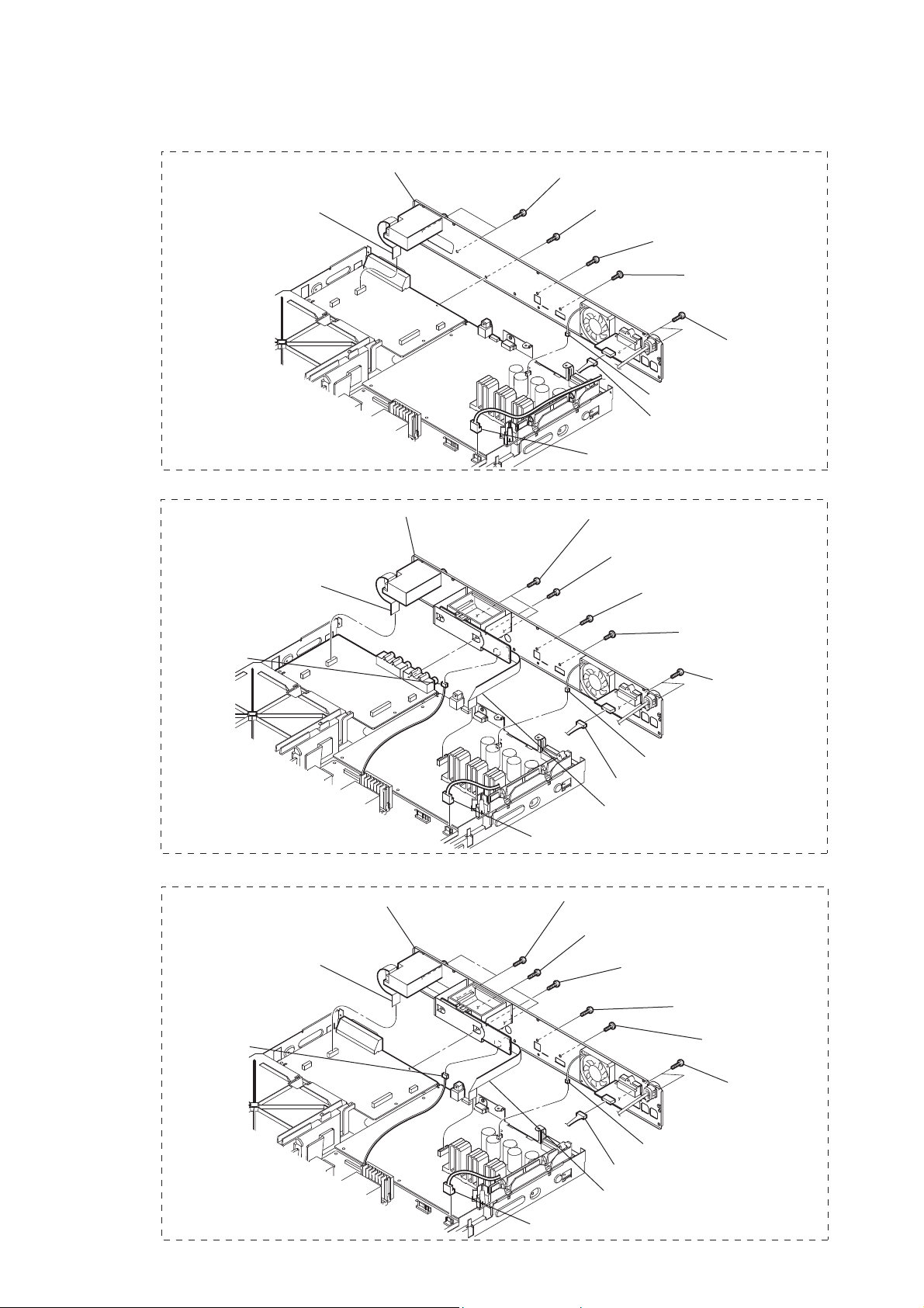
Arranging the USB wire
USB wire
Tie up with LP501.
800:/2W
Point of capacitor discharge for C903:
Connect to the foot of C903.
The USB wire should be located on the front side
from these capacitors.
Have the USB wire spread on the inside
of the claws of the chassis.
Thread the USB wire through the capacitors.
Dress the USB wire in this area
properly along the board.
USB wire
MAIN board
7

HBD-DZ330/DZ710/DZ730
DISASSEMBLY
• This set can be disassembled in the order shown below.
SET
2-1. CASE
(Page 9)
SECTION 2
2-2. LOADING PANEL
(Page 10)
2-9. POWER BOARD
(Page 15)
2-3. FRONT PANEL SECTION
(Page 10)
2-4. FL BOARD,
ENCODER BOARD,
JACK BOARD,
USB BOARD
(Page 11)
2-6. BACK PANEL SECTION
(Page 13)
2-7. MAIN BOARD
(Page 14)
2-10. DVD MECHANISM DECK SECTION
(Page 16)
2-11. TRAY
(Page 16)
2-8. IO BOARD
(Page 15)
2-5. KEY-SW BOARD,
P-SW BOARD
(Page 12)
2-12. BELT
(Page 17)
2-13. MS-203 BOARD
(Page 17)
2-14. BASE UNIT
(Page 18)
2-15. OPTICAL PICK-UP
(Page 18)
8

Note: Follow the disassembly procedure in the numerical order given.
2-1. CASE
4 screw
(+BV3 (3-CR))
5
HBD-DZ330/DZ710/DZ730
3 four screws
(+BV3 (3-CR))
2 two screws
(+BV3 (3-CR))
1 two screws
(+BV3 (3-CR))
8 case
7
6 Raise one side of the case.
9

HBD-DZ330/DZ710/DZ730
2-2. LOADING PANEL
3 loading panel
Insert a screwdriver from between the front panel
and the chassis and slide the rod in the direction
of the arrow.
2-3. FRONT PANEL SECTION
2 two ground plate (front)
8 claw
1
tray
2
1 two screws
(+BV3 (3-CR))
qa CN5202 (4P)
0
10
6 four claws
9 three claws
4 nut
3 knob vol (DSZ)
7 claw
qs front panel section
5 four screws
(+BV3 (3-CR))

2-4. FL BOARD, ENCODER BOARD, JACK BOARD, USB BOARD
8 CN4007 (4P) (DZ330/DZ730)
CN4011 (4P) (DZ710)
HBD-DZ330/DZ710/DZ730
qa CN2101 (5P)
2 screw
(+BV3 (3-CR))
4 CN5006 (2P) (DZ330/DZ730)
CN5003 (4P) (DZ710)
1 wire (flat type) (13 core) (CN5005)
(DZ330/DZ730)
wire (flat type) (15 core) (CN5002)
(DZ710)
Arranging the USB wire
5 FL board
3 screw
(+BV3 (3-CR))
9 two screws
(+BV3 (3-CR))
7 ENCODER board
0 JACK board
6 claw
qs screw
(+BV3 (3-CR))
qd JACK board
USB wire
Tie up with LP501.
The USB wire should be located on the front side
from these capacitors.
Thread the USB wire through
the capacitors.
Dress the USB wire in this area
properly along the board.
USB wire
MAIN board
Have the USB wire spread on the inside
of the claws of the chassis.
11

HBD-DZ330/DZ710/DZ730
2-5. KEY-SW BOARD, P-SW BOARD
1 CN5301 (2P)
3 eight claws
escutcheon (DSZ)
2 five screws
(+BTP 2 u6)
4
8 KEY-SW board
6 P-SW board
12
7 two claws
5 two claws
2-6. BACK PANEL SECTION
DZ330
4 wire (flat type) (11 core)
(CN4009)
0 back panel section (DZ330)
HBD-DZ330/DZ710/DZ730
6 two screws
(+BVTP 3 u8)
5 screw
(+BVTP 3 u8)
7 screw
(+BVTP 3 u8)
8 screw
(+B 3 u6)
9 two screws
(+BVTP 3 u8)
3 CN3000 (2P)
2 CN5401 (4P)
1 CN901 (2P)
DZ710
5 wire (flat type) (11 core)
(CN4009)
6 CN102 (2P)
DZ730
5 wire (flat type) (11 core)
(CN4009)
6 CN102 (2P)
qs back panel section (DZ710)
qd back panel section (DZ730)
8 two screws
(+BVTP 3 u8)
7 screw
(+BVTP 3 u8)
9 screw
(+BVTP 3 u8)
0 screw
(+B 3 u6)
qa two screws
(+BVTP 3 u8)
3 CN3000 (2P)
2 CN5401 (4P)
4 wire (flat type) (12 core)
(CN306)
1 CN901 (2P)
9 two screws
(+BVTP 3 u8)
8 two screws
(+BVTP 3 u8)
7 screw
(+BVTP 3 u8)
0 screw
(+BVTP 3 u8)
qa screw
(+B 3 u6)
1 CN901 (2P)
qs two screws
(+BVTP 3 u8)
3 CN3000 (2P)
2 CN5401 (4P)
4 wire (flat type) (12 core)
(CN306)
13

HBD-DZ330/DZ710/DZ730
2-7. MAIN BOARD
6 wire (flat type) (11 core) (CN471)
(DZ330/DZ730)
wire (flat type) (9 core) (CN472)
(DZ710)
5 wire (flat type) (24 core) (CN1101)
7 wire (flat type) (19 core) (CN504)
(DZ330/DZ730)
wire (flat type) (21 core) (CN505)
(DZ710)
8 CN1501 (6P)
9 wire (flat type) (5 core)
(CN1502)
qh two screws
(+BV3 (3-CR))
qd four screws
(+BV3 (3-CR))
qf heat sink
4 CN2101 (5P)
qg five screws
(+BV3 (3-CR))
1 wire (flat type) (13 core) (CN507)
(DZ330/DZ730)
wire (flat type) (15 core) (CN506)
(DZ710)
Arranging the USB wire
USB wire
qj MAIN board
3 CN904 (5P)
2 CN906 (11P)
The USB wire should be located on the front side
from these capacitors.
0 two screws
(+BV3 (3-CR))
qs shield plate (PC-DSZ)
When the heat sink
has been removed,
apply oil compound
(G-747) to it.
qa insulated plate
(PC-DSZ)
14
Tie up with LP501.
Thread the USB wire through
the capacitors.
Dress the USB wire in this area
properly along the board.
USB wire
MAIN board

2-8. IO BOARD
4 two screws
(+BV3 (3-CR))
5 IO board
HBD-DZ330/DZ710/DZ730
1 CN4007 (4P) (DZ330/DZ730)
CN4011 (4P) (DZ710)
2 wire (flat type) (11 core) (CN4001)
(DZ330/DZ730)
wire (flat type) (9 core) (CN4002)
(DZ710)
3 wire (flat type) (19 core) (CN4005)
(DZ330/DZ730)
wire (flat type) (21 core) (CN4006)
(DZ710)
2-9. POWER BOARD
5 four screws
(+BV3 (3-CR))
8 POWER board
1 CN102 (2P) (DZ710/DZ730)
4 CN906 (11P)
3 CN904 (5P)
2 CN901 (2P)
6 four screws
(+BV3 (3-CR))
7 holder PC board
15

HBD-DZ330/DZ710/DZ730
2-10. DVD MECHANISM DECK SECTION
5 two screws
(+BV3 (3-CR))
8 two screws
(+BV3 (3-CR))
0 DVD mechanism deck
2 wire (flat type) (5 core)
(CN1502)
1 wire (flat type) (13 core) (CN507)
(DZ330/DZ730)
wire (flat type) (15 core) (CN506)
(DZ710)
6 screw
(+BV3 (3-CR))
7 cover (CDM-DSZ)
9 screw
(+BV3 (3-CR))
3 CN1501 (6P)
4 wire (flat type) (24 core)
(CN1101)
2-11. TRAY
1 Move the chuck cam
in the direction of the arrow.
bottom side
3 two claws
2
4
5 tray
16

2-12. BELT
2
chuck cam
3
HBD-DZ330/DZ710/DZ730
belt
2-13. MS-203 BOARD
3
MS-203 board
4
DC motor
1 two claws
2 three claws
1 screw
(M 1.7 u 2.5)
17

HBD-DZ330/DZ710/DZ730
2-14. BASE UNIT
2
chuck cam
3 two claws
1 two claws
4 base unit
2-15. OPTICAL PICK-UP
4 two insulator screws
2 FFC holder
3 two insulator screws
1 two claws
6 two insulators
5 two insulators
7 optical pick-up
(KHM-313CAA)
18

SECTION 3
TEST MODE
HBD-DZ330/DZ710/DZ730
Note: Incorrect operations may be performed if the test mode is not
entered properly.
In this case, press the [?/1] button to turn the power off, and
retry to enter the test mode.
1. Cold Reset
• The cold reset clears all data including preset data stored
in the RAM to initial conditions. Execute this mode when
returning the set to the customers.
Procedure:
1. Press the [
2. Press three buttons [
] button to turn the power on.
?/1
], [FUNCTION] and [
N
] simultane-
?/1
ously.
3. When this button is operated, display as “COLD RESET” for
a while and all of the settings are reset.
2. Panel Test Mode
• This mode is used to check the software version, FL and
KEY.
2-1. Display Test Mode
Procedure:
1. Press the [
] button to turn the power on.
?/1
2. While pressing the [x] and the [N] buttons simultaneously,
turn the [VOLUME] control in the direction of (+).
3. When the display test mode is activated, all segments are
turned on. When the mode in, “REC TO USB” is turn off.
4. To exit from this mode, while pressing the [x] and the [N]
buttons simultaneously, turn the [VOLUME] control in the direction of (+).
2-2. Version Test Mode
Procedure:
1. When the display test mode is activated, press the [FUNCTION] button and the message “DSZ2E” (DZ330), “DSZ6KD”
(DZ710), “DSZ5E” (DZ730) are displayed, the version test
mode is activated.
2. Whenever the [FUNCTION] button is pressed, the display
changes in the following order.
“DSZ2E” (Model name) t “NA*1” (Destination) t MC V ersion
*1: NA changes depending on destination.
3. Press the [REC TO USB] button when the MC version is on
display. The date of software production is displayed.
4. Press the [REC TO USB] button again and the version is displayed.
5. To exit from this mode, while pressing the [x] and the [N]
buttons simultaneously, turn the [VOLUME] control in the direction of (+).
2-3. FL Pattern Test Mode
Procedure:
1. When the display test mode is activated, press the [Z] button,
to select the FL pattern test mode. When the FL pattern test
mode, half segments of FL display and “REC TO USB” are
turn on.
2. Press the [Z] button, half segments of FL display and “REC
TO USB” are turn off.
3. Next press the [
] button, all segments of FL display is turn
Z
on.
4. To exit from this mode, while pressing the [
] and the [N]
x
buttons simultaneously, turn the [VOLUME] control in the direction of (+).
2-4. Key Test Mode
Procedure:
1. When the display test mode is activated, press the [
?/1
] but-
ton, to select the key test mode.
2. To enter the KEY test mode, the fl uorescent indicator displays
“K0 V0”. Each time an another button is pressed, “KEY” value
increases. However, once a button is pressed, it is no longer
taken into account. When all keys are pressed correctly, “K6
V0” is displayed.
3. When the [VOLUME] control is turned in the direction of (+),
“V0” is changed to “V1”, then ... “V9”.
When the [VOLUME] control is turned in the direction of (–),
“V0” is changed to “V9”, then ... “V1”.
4. To exit from this mode, while pressing the [
] and the [N]
x
buttons simultaneously, turn the [VOLUME] control in the direction of (+).
3. Disc Tray Lock
• The disc tray lock function for the antitheft of an demonstra-
tion disc in the store is equipped.
Setting Procedure :
1. Press the [
] button to turn the set on.
?/1
2. Press the [FUNCTION] button to set DVD function.
3. Insert a disc.
4. Press the [x] button and the [Z] button simultaneously for fi ve
seconds.
5. The message “LOCKED” is displayed and the tray is locked.
Releasing Procedure :
1. Press the [x] button and the [Z] button simultaneously for fi ve
seconds again.
2. The message “UNLOCKED” is displayed and the tray is unlocked.
Note: When “LOCKED” is displayed, the tray lock is not released by
turning power on/off with the [?/1] button.
4. DVD Version Display
• The STR and DVD microprocessor versions are displayed.
Procedure:
1. Press the [
2. Press the [N] button and the [
] button to turn the set on.
?/1
] button simultaneously for
?/1
three seconds. SC version display is presented.
3. Pressing the [FUNCTION] button presents a DV version display. Pressing the [FUNCTION] button again returns to the SC
version display.
4. To exit from this mode, press any button other than the [FUNCTION] button.
5. Product Out
• This mode moves the optical pick-up to the position durable
to vibration and clears all data including preset data stored
in the STR RAM to initial conditions. Use this mode when
returning the set to the customer after repair.
Procedure:
1. Press the [
] button to turn the power on.
?/1
2. Press the [FUNCTION] button to set the function “DVD/CD”.
3. Remove all discs.
4. While pressing the [x] and the [Z] buttons simultaneously,
turn the [VOLUME] control in the direction of (+).
5. Displayed to message “SERVICE IN” on the fl uorescent indi-
cator tube when pressing in turn the [4] t [DVD MENU] t
[CLEAR] buttons on the remote commander.
6. After the “STANDBY” blinking display fi nishes, the message
“MECHA LOCK” h “UNPLUG” is displayed on the fl uo-
rescent indicator tube disconnect the AC power plug, then the
product out mode is set.
The STR RAM initialization is executed upon a next power-on
after the power is turned off.
19

HBD-DZ330/DZ710/DZ730
6. D.C.A.C. (AUTOMATIC ACOUSTIC FIELD CALIBRATION) TEST MODE
Procedure:
1. Press the [
] button to turn the power on.
?/1
2. Press the [FUNCTION] button to set the function “ DVD/CD”.
3. Insert Calibration mic (ECM-AC2) supplied as an accessory
into the A.CAL MIC jack.
4. Press three buttons [x], [Z] and [REC TO USB] simultaneously.
5. Confi rm that the following are shown on the display panel.
The JACK inserted/non-inserted detection display and the dis-
play.
* * * * * * * *
123
1 MIC detection condition
NON : Not detected
IN : Detected
2 Presence of DIGITAL sound data input to the microprocessor
NG: Input absent
OK: Input present
3 AD value (255h) of MIC input to the microprocessor
6. T o exit from this mode, press three buttons [x], [Z] and [REC
TO USB] simultaneously.
7. PROTECTION FACTOR (SD DETECTION/
DC DETECTION/TSD DETECTION) IDENTIFICATION
TEST MODE
When an error is detected, the FL tube alternately displays
“PROTECTOR h PUSH POWER”.
r Press the [
* Buttons other than the [
?/1
] button.
] button are invalid.
?/1
“STANDBY” blinks three times on the FL tube.
r
The protection release state (POWER OFF) is established.
(No FL tube display)
r Press the [
] button two times.
?/1
The power to the system turns on, and the normal operation is
established. (Restore)
During the protection state:
1. If the AC plug is connected or disconnected during the protection state, the protection state is released, and the normal operation is established. (The protection state is not maintained.)
2. The protection factor is displayed by pressing the [RETURN]
t [3] t [2] t [0] t [0] t [ANGLE] buttons of the remote commander.
(during the “PROTECTOR” h “PUSH POWER” display).
k When SD is detected: Repeats
“SD DETECT” h “PROTECTOR”.
k When DC is detected: Repeats
“DC DETECT” h “PROTECTOR”.
k When TSD is detected: Repeats
“TMP DETECT” h “PROTECTOR”.
PL: SD detection
When the “L” output from the SD (shutdown) port on the
S-MASTER POWER Driver Shutdown and voltage descent
(15V or less) of 30V power supply (PVDD) are detected.
DC detection
When the “L” output from the power/speaker error detection
circuit (DC detection port) is detected for two seconds continually, the power system other than that of the FL tube is
turned off, and the protection state is established.
TSD detection
When the “L” output from the thermal shutdown port
(TSDM) on the motor driver is detected.
20
HBD-DZ330/DZ710/DZ730
DVD SECTION
8-1. GENERAL DESCRIPTION
• The IOP measurement allows you to make diagnosis and adjustment simply by using the remote commander and monitor TV. The instructions, diagnosis results, etc. are given on
the on-screen display (OSD).
Be sure to execute the IOP measurement when a BU (Base
Unit) is replaced.
8-2. HOW TO ENTER TEST MODE
While pressing the [
the [VOLUME] control in the direction of (+) with the DVD player in power on.
The Test Mode starts, displayed “SERVICE IN” on this model
display then the menu shown below will be displayed on the TV
screen.
* The display of the “Model Name” of the “Remocon Diagnosis
Menu” change with the model and the destination. Refer to
below on the model name.
DZ330 : DSZ2E
DZ710 : DSZ6KD
DZ730 : DSZ5E
0. External Chip Check
1. Servo Parameter Check
2. Drive Manual Operation
3. Emergency History
4. Version Information
5. USB Test Mode Setting
Model Name
IF-con : Ver. XX.XX (XXXX)
Syscon : Ver. X.XXX
*1: Changes depending on destination
The menu above is the Remocon Diagnosis Menu screen which
consists of fi ve main functions. At the bottom of the menu screen,
the model name and IF-con version. To exit from the Test Mode,
press the [
] button on the remote commander.
?/1
8-3. EXECUTING IOP MEASUREMENT
In order to execute IOP measurement, the following standard procedures must be followed.
(1) In power on, while pressing the [x] and the [Z] buttons simul-
taneously, turn the [VOLUME] control in the direction of (+).
0. External Chip Check
1. Servo Parameter Check
2. Drive Manual Operation
3. Emergency History
4. Version Information
5. USB Test Mode Setting
Model Name : DSZ2E_XX
IF-con : Ver. XX.XX (XXXX)
Syscon : Ver. X.XXX
*1: Changes depending on destination
] and the [Z] buttons simultaneously, turn
x
Remocon Diagnosis Menu
1
: DSZ2E_XX
Remocon Diagnosis Menu
*
1
*
(2) Select “2. Drive Manual Operation” by pressing the [2] button
on the remote commander. The screen will appear as shown.
Drive Manual Operation
1. Servo Control
2. Track/Layer Jump
3. Manual Adjustment
4. Tray Aging Mode
5. MIRR time adjust
0. Return to Top Menu
(3) Select “3. Manual Adjustment” by pressing the [3] button on
the remote commander. The screen will appear as shown.
Manual Adjust
1. Track Balance Adjust:
2. Track Gain Adjust:
3. Focus Balance Adjust:
4. Focus Gain Adjust:
5. Eq Boost Adjust:
6. Iop:
7. TRV. Level:
8. S curve(FE) Level:
9. RFL(PI) Level:
0. MIRR Time:
Oo Change Value
[RETURN] Return to previous menu
(4) Select “6. IOP” by pressing the [6] button on the remote com-
mander.
(5) Wait until a hexadecimal number appear.
Manual Adjust
1. Track Balance Adjust:
2. Track Gain Adjust:
3. Focus Balance Adjust:
4. Focus Gain Adjust:
5. Eq Boost Adjust:
6. Iop. 47:
7. TRV. Level:
8. S curve(FE) Level:
9. RFL(PI) Level:
0. MIRR Time:
Oo Change Value
[RETURN] Return to previous menu
(6) Convert each data from hexadecimal to decimal using conver-
sion table.
(7) Please fi nd the label on the rear of the BU (Base Unit).
The default IOP value is written in the label.
(8) Subtract between these two values.
(9) If the remainder is smaller than 93 (decimal), then it is OK.
However if the value is higher than 93, then the BU is defective and need to be change.
(10) Press the [RETURN] button on the remote commander to re-
turn back to previous menu.
(11) Press the [0] button on the remote commander to return to T op
Menu.
21

HBD-DZ330/DZ710/DZ730
8-4. EMERGENCY HISTORY
To check the emergency history, please follow the following procedure.
(1) From the Top Menu of Remocon Diagnosis Menu, select “3.
Emergency History Check” by pressing the [3] button on the
remote commander. The following screen appears on the onscreen display.
Emg. History Check
Laser Hours CD 999h 59min
01. 01 05 04 04
00 00 00 00 00 00 23 45
02. 02 02 01 01 00 A9 4B 00
00 00 00 00 00 00 23 45
[Next] Next Page [Prev] Prev Page
[O] Return to Top Menu
DVD 999h 59min
00 92 46 00
(2) Y ou can check the total time when the laser is turned on during
playback of DVD and CD from the above menu. The maximum time, which can be displayed are 999h 59min.
(3) You can check the error code of latest 10 emergency history
from the above menu. To view the previous or next page of
emergency history, press [.] or [>] button on the remote
commander. The error code consists of the following three
blocks. The fi rst block indicates the error code. The second
block indicates the parameter and the third block indicates the
time of error code as shown below.
60: Focus on error
61: Seek fail error
62: Read Q data/ID error
70: Lead in data read fail
71: TOC read time out (CD)
80: Can’t buffering
81: Unknown media type
8-4-1. Clear the Laser Hour
Press [
DISPLA Y] button and then press [CLEAR] button on the
remote commander. The data for both CD and DVD data are reset.
Emg. History Check
Laser Hours CD 0h 0min
01. 01 05 04 04
00 00 00 00 00 00 23 45
02. 02 02 01 01 00 A9 4B 00
00 00 00 00 00 00 23 45
[Next] Next Page [Prev] Prev Page
[O] Return to Top Menu
DVD 0h 0min
00 92 46 00
8-4-2. Clear the Emergency History
Press [DVD TOP MENU] button and then press [CLEAR] button
on the remote commander. The error code for all emergency history would be reset.
Emg. History Check
• Error Code
Emg. History Check
Laser Hours CD 999h 59min
*1 *2
01. 01 05 04 04
00 00 00 00 00 00 23 45
02. 02 02 01 01 00 A9 4B 00
00 00 00 00 00 00 23 45
[Next] Next Page [Prev] Prev Page
[O] Return to Top Menu
DVD 999h 59min
00 92 46 00
*3
*1 : Error Code
*2 : Parameter of error code
*3 : Time of error code
The meaning of error code is as below:
01: Communication error (No reply from syscon)
02: Syscon hung up
03: Power OFF request when syscon hung up
19: Thermal shutdown
24: MoveSledHome error
25: Mechanical move error (5 Changer)
26: Mechanical move stack error
30: DC motor adjustment error
31: DPD offset adjustment error
32: TE balance adjustment error
33: TE sensor adjustment error
34: TE loop gain adjustment error
35: FE loop gain adjustment error
36: Bad jitter after adjustment
40: Focus NG
42: Focus layer jump NG
51: Spindle stop error
52: Open kick spindle error
Laser Hours CD 999h 59min
01. 00 00 00 00
00 00 00 00 00 00 00 00
02. 00 00 00 00 00 00 00 00
00 00 00 00 00 00 00 00
[Next] Next Page [Prev] Prev Page
[O] Return to Top Menu
DVD 999h 59min
00 00 00 00
8-4-3. Clear the Initialize Setup Data
Press [DVD MENU] button and then press [CLEAR] button on the
remote commander.
Emg. History Check
Laser Hours CD 999h 59min
[Next] Next Page [Prev] Prev Page
[O] Return to Top Menu
DVD 999h 59min
initialize setup data...
8-4-4. Return to the Top Menu of Remocon Diagnosis
Menu
Press [0] button on the remote commander.
22

HBD-DZ330/DZ710/DZ730
SECTION 4
ELECTRICAL ADJUSTMENTS
8-5. CHECK VERSION INFORMATION
To check the version information, please follow the following procedure.
(1) From the Top Menu of Remocon Diagnosis Menu, select “4.
Version Information” by pressing the [4] button on the remote
commander. The following screen appears on the on-screen
display.
Version information
Firm (Main) : Ver. xxxxx
Firm (Sub) : xxxxx
RISC : xxxxx
8032 : xxxxx
Audio DSP : xxxxx
Servo DSP : xxxxx
Phy,Adr, : F.F.F.F
[O] Return to Top Menu
To return to the Top Menu of Remocon Diagnosis Menu, press
[0] button on the remote commander.
DVD SECTION
When the optical pick-up assy is replaced, perform the “EXECUT ING IOP MEASUREMENT”.
EXECUTING IOP MEASUREMENT (See page 21)
TUNER SECTION
[FM Tune Level Check]
generator
SET
Procedure:
1. Turn the power on.
2. Input the following signal from Signal Generator to FM antenna input directly.
FM ANTENNA
OUT (75 :)
* Carrier Freq : A = 87.5 MHz, B = 98 MHz, C = 108 MHz
Deviation : 75 kHz
Modulation : 1 kHz
ANT input : 35 dBu (EMF)
Note: Please use 75 ohm “coaxial cable” to connect SG and the set. You
cannot use video cable for checking.
Please use SG whose output impedance is 75 ohm.
3. Set to FM tuner function and tune A, B and C signals.
4. Confi rm “TUNED” is lit on the display for A, B and C signals.
The mark of “TUNED” means “The selected station signal is received in good condition.”
23

HBD-DZ330/DZ710/DZ730
SECTION 5
DIAGRAMS
THIS NOTE IS COMMON FOR PRINTED WIRING BOARDS AND SCHEMATIC DIAGRAMS.
(In addition to this, the necessary note is printed in each block.)
For Printed Wiring Boards.
Note:
• X : Parts extracted from the component side.
• a : Through hole.
• : Pattern from the side which enables seeing.
(The other layers’ patterns are not indicated.)
Caution:
Pattern face side:
(SIDE B)
Parts face side:
(SIDE A)
• Indication of transistor.
C
Q
B
E
CEB
• Abbreviation
RU : Russian model
These are omitted.
Parts on the pattern face side seen
from the pattern face are indicated.
Parts on the parts face side seen from
the parts face are indicated.
These are omitted.
For Schematic Diagrams.
Note:
• All capacitors are in μF unless otherwise noted. (p: pF) 50
WV or less are not indicated except for electrolytics and
tantalums.
• All resistors are in Ω and 1/4 W or less unless otherwise
specifi ed.
• f : Internal component.
• C : Panel designation.
Note: The components identifi ed by mark 0 or dotted
line with mark 0 are critical for safety.
Replace only with part number specifi ed.
• A : B+ Line.
• B : B– Line.
• Voltages and waveforms are dc with respect to ground
under no-signal (detuned) conditions.
• Voltages and waveforms are dc with respect to ground in
service mode.
• Waveforms are taken with a oscilloscope.
Voltage variations may be noted due to normal production
tolerances.
no mark : TUNER (FM)
< > : DVD PLAY
* : Impossible to measure
• Voltages are taken with VOM (Input impedance 10 MΩ).
• Circled numbers refer to waveforms.
• Signal path.
F : TUNER
J : DVD PLAY
L : VIDEO
r : COMPONENT VIDEO
N : MIC
d : AUDIO IN
• Abbreviation
RU : Russian model
• Circuit Boards Location
P-SW board
MS-203 board
FL board
IO board
KEY-SW board
JACK board
S-AIR CON board (DZ710/DZ730)
MAIN board
SPEAKER board
POWER board
USB board
ENCODER board
24

5-1. BLOCK DIAGRAM – RF Section –
RF
VOA/A
DETECTOR
OPTICAL PICK-UP
BLOCK
(KHM-313CAA)
VOB/B
VOC/C
VOD/D
VOE/E+G
VOF/F+H
A
B
C
D
A
B
C
D
VC
(2.0V)
10
6
7
8
9
17
18
11
12
13
14
28
DVDRFIP
DVDA
DVDB
DVDC
DVDD
TNI
TPI
MA
MB
MC
MD
V20
CD/DVD RF AMP,
FOCUS/TRACKING ERROR AMP,
DVD SYSTEM CONTROL, DSP
IC1101 (1/3)
V2REFO
RXD
TXD
MC_DATA (ADIN)
HBD-DZ330/DZ710/DZ730
CN1105
6
27
105
106
206
(2.8V)
A/D CONVERTER
DOUT
9
SCKI
6
LRCK
7
BCK
8
IC303
VINL
VINR
RFMON
5
V2REFO
RXD
TXD
(SERVICE JIG)
L-IN
R-IN
B
(Page 27)
AUDIO
SECTION
2
1
13
14
LASER
DIODE
(FOR CD)
LASER
DIODE
(FOR DVD)
(LO:DVD, HI:CD) MSW
2AXIS
DEVICE
FOCUS/
TRACKING
COIL
LD (780)
LD (650)
VR (650)
VR (780)
VCC
FCS+
FCS-
TRK+
TRK-
PD
(SPINDLE MOTOR)
REG02
REG01
(SLED MOTOR)
LD DRIVE
(FOR CD)
Q1102 (1/2)
LD DRIVE
(FOR DVD)
Q1102 (2/2)
PD VOLUME
CONTROL
Q1101
Q1103
MM
MM
SP+
SP-
SLSL+
IOP
LD01
22
MDI1
19
MDI2
20
LD02
21
MSW
54
FOCUS/TRACKING DRIVER,
LOADING/SPINDLE/SLED MOTOR DRIVER
OPIN+
28
OPIN–
29
VO1+
6
FOCUS COIL
VO1–
7
VO2–
9
TRACKING COIL
VO2+
8
MUTE123
34
2
11
VO3–
VO3+
VO4+
VO4–
REG DRIVER
SLED MOTOR
SPINDLE MOTOR
39
10
12
13
IC1501
BUFFER
DRIVE
DRIVE
DRIVE
DRIVE
STBY
LOADING
CONTROL
OPOUT
FWD
REV
VCTL
TSDM
BUS BUFFER
IC471
ACLK
203
ALRCK
205
ABCK
204
ASDATA2
223
ASDATA1
225
ASDATA0
226
ASDATA3
222
(LIMITSW)
LIMITSW
53
30
VCI
26
IN1
24
IN2
23
IN3
22
IN4
21
19
20
18
36
27
34
35
14
15
IOPMON
VREFO
FOO
TRO
FMO
DMO
FWD
REV
TROPENPWM
REGRST
SPFG
MUTE
TSD_M
FMO
FOO
DMO
TRO
39
IOPMON
VREFO
29
FMO
37
FOO
41
DMO
36
TRO
40
FWD
94
REV
95
38
TROPENPWM
REGRST
157
OP_INP
35
MUTE
158
TSD_M
130
XSYSRST
IFCK
IFSDO
IFSDI
XIFCS
KRMOD
MIC
OCSW
IFBSY
CKSW
108
98
97
100
99
213
208
104
110
103
XSYSRST
IFSCK
IFSDO
IFSDI
XIFCS
KRMOD
MIC
2 18
4 16
5 15
6 14
7 13
8 12
9 11
SYSTEM CONTROL
IC503 (1/5)
MTK_RST
45
DVD_SCO
49
DVD_SOD
48
DVD_SID
47
DVD XIFCS
51
KARAOKE MODE
53
TV_SEL/MIC_DET_OUT
52
CDM_OPEN_SW
44
DVD_XIFBUSY
50
TV_SEL
XSYSRST
XSYSRST
I
C
D
OCSW1/REVOCSW
CKSW/FWDCKSW
LDM+
LDM-
DZ710
VIDEO
SECTION
(Page 26)
VIDEO
SECTION
(Page 26)
AUDIO
SECTION
(Page 27)
S001
(CHUCK/TRAY DETECT)
AMP_D3
AMP_D2
AMP_D1
AMP_D0
DZ330/DZ730
M
(LOADING MOTOR)
MCKO
LRCKO
BCKO
x SIGNAL PATH
M001
AMP
A
SECTION
(Page 28)
: TUNER
: DVD PLAY
HBD-DZ330/DZ710/DZ730
2525

HBD-DZ330/DZ710/DZ730
5-2. BLOCK DIAGRAM – VIDEO Section –
SYSTEM CONTROL
IC503 (2/5)
CEC_TX_RX
17
82V_SEL1
81V_SEL0
72HDMI_PCONT
209WIDE
210RGB_SEL/DSEL
187CVBS
185Y/G
183B/Cb/Pb
182R/Cr/Pr
CEC_TX_OUT
DZ710/DZ730
DZ330/DZ730
RF
SECTION
(Page 25)
INHIBIT SWITCH
I
Q4003
TV_SEL
+5V
(IO)
FUNCTION SWITCH
CONTROL (TV/WIDE/PART)
Q4002, 4004 (1/2)
13 MUTE2
3MUTE1
4 CVBSIN
10 CVIN
12 CBIN
14 CRIN
A12V
VIDEO DRIVER
IC4000
D4001
CN4000 (1/2)
19
CVBS OUT
11
G OUT
B OUT
7
15
R/C OUT
8
FUNCTION SW
BLACKING CONTROL
(CVBS RGB)
Q4000, 4001, 4004 (2/2)
23CVBSOUT
20CYOUT
18CbOUT
16CrOUT
VOUT
CYOUT
CBOUT
CROUT
16
J4001 (1/2)
J4000
BLANKING OUT
VIDEO OUT
Y
PB/CB
PR/CR
T
COMPONENT
VIDEO OUT
DZ330/DZ730
EURO AV
OUTPUT (TO TV)
DZ710
DVD SYSTEM CONTROL, DSP
IC1101 (2/3)
SCL
SDA
112 101 102
7
6
5
WE EEWP
SCL
SDA
EEPROM
IC1103
180TX2P
179TX2N
177TX1P
176TX1N
174TX0P
173TX0N
171TCKP
170TCKN
162HTPLG
12
I2C_SCL
FLASHROM
IC1601
UK MODEL
13
I2C_SDA
4
RESET
RF
SECTION
(Page 25)
4
DZ710/DZ730
C
1
2
XSYSRST
BUFFER
IC1705
12
79,80,82–86,89
HD0–HD7
HD0–HD7
29,31,33,35,
38,40,42,44
RESET
D+3.3V
DZ330
HD0–HD7
DQ0–DQ7
HA0–HA21
56–64,67–75,77,
A0–A21
A0
25–16,10–1,48
A0–A19,N.CDQ15/A-1
FLASH ROM
IC1102
87,91,92
A1–A21
+6V
XRD
XROMCS
76
XWR
11OE28CE2645
WE
+5V REG.
IC1707
XWR
XRD78XROMCS
66
161
DDC_CLK
RD0–RD15
117–113,119–129
2,4,5,7,8,10,11,13,42,
44,45,47,48,50,51,53
RD0–RD15
159
DDC_DA
LEVEL SHIFT
Q1701
RA0–RA11
139–141,143,144
149–155
22–26,29–35
RA0–RA11
SDRAM
IC1104
CEC_TX_OUT
DRCLK
BA1
BA0
146
138
137
38
20
BA121BA0
CLK
_RCS
133
136
16
19
/CS
LEVEL SHIFT
Q9730
_CAS
_RAS
_RWE
111
134
135
15
18
/WE
/CAS17/RAS
DQM0
132
39
LDQM
DQM1
147
37
UDQM
CKE
CLKE
CN1701
1
TMDS DATA2 +
3
TMDS DATA2 –
4
TMDS DATA1 +
6
TMDS DATA1 –
7
TMDS DATA0 +
9
TMDS DATA0 –
10
TMDS CLOCK +
12
TMDS CLOCK –
19
HPD
18
+5V POWER
13
CEC
RESERVED
14
15
SCL
16
SDA
BUFFER
IC701
1 2
1A 3Y
HDMI OUT
SPDIF-ARC
ARC
E
x SIGNAL PATH
AUDIO
SECTION
(Page 27)
: VIDEO
: COMPONENT VIDEO
HBD-DZ330/DZ710/DZ730
2626

5-3. BLOCK DIAGRAM – AUDIO Section –
HBD-DZ330/DZ710/DZ730
+9V
DZ710
DZ710
J5101
MIC1/
A.CAL MIC
J5102
MIC2
DZ330/
DZ730
J5101
A.CAL MIC
J5102
AUDIO IN
TV
OUTPUT (TO TV)
T
AUDIO
IN
EURO AV
J4001(2/2)
L
R
J4000(2/2)
MIC BIAS
DZ330/DZ730
DZ710
DZ710
R-CH
DZ330/DZ730
A (L) IN
6
A (R) IN
2
R-CH
R-CH
SWITCH
Q5101,5102
MIC AMP
IC5101
5 7 3 1
LINE AMP/MIC AMP
IC5102
3 1
ELECTRONIC VOLUME
IC4004
7
VOUT2
2 1
VOUT1
MIC AMP ALC
IC4006
ALC
14
VIN2
VIN1
DATA
CLK
D5006
8
4
5
4
5
DC_CONT
PULG_DET
A.CAL
MIC
FUNCTION
SELECTOR
IC4003
5 3
Y1 Y
2
Y2
4
Y3
10
A
1
Y0
L
5 3
2
4
1
Y1 Y
Y2
Y3
Y0
FUNCTION
SELECTOR
IC4002
9
B
10
A
9
B
Q4006
Q4005
R-CH
L-IN
R-IN
ASEL0
ASEL1
DZ730
ASEL2
DZ730
B
ASEL0
ASEL1
ASEL2
PULG_DET
RF
SECTION
(Page 25)
AMP
SECTION
(Page 28)
ASEL0
84
ASEL1
85
ASEL2
86
MIC/A.CAL_SW/MIC2_SW
65
F
S-AIR_ADC_SEL
SD2
SD1
BCK
S-AIR_DET
S-AIR_SDA
S-AIR_CLK
S-AIR_RST
GPIO2
R-CH
36
38
30
29
37
35
DZ730
Rch
Lch
SD2
SD1
BCK1
BCK2
LRCK1LRCK
LRCK2
GND (for DET)
ADC_SEL
I2C_SDA
I2C_SCL
RESN
GPIO2
CN103
2
4
26
16
15
24
(S-AIR TRANSMITTER)
14
23
25
12
19
18
11
7
DZ710/DZ730
CN103
'<96
TV DIGITAL IN
ANTENNA
75: FM
COAXIAL
OPTICAL
TU4001
FM
TUNER
PACK
OPTICAL
RECEIVER
IC502
L-CH
R-CH
TUNED
DI
DO
CK
CE
RDS_DATA
RDS_CLK
R-CH
VIDEO
SECTION
(Page 26)
SECTION
(Page 25)
7
POWER
SECTION
(Page 29)
A.CAL
DC_CONT
MIC_DATA
MIC_CLK
TUNED
DI
DO
CK
CE
RDS_DATA
RDS_CLK
VBUS
DD+
GND
DZ710
DIR
SPDIF-ARC
E
X301
24.576MHz
RF
XSYSRST
D
4
21
22
52
48 25
IC304
DIN1 (I)
XOUT (O)
XIN (I)
DIN2 (I)
XMODE (I) XVOICE/DIR_CSFLAG
AUDIO- (O)
24
ERROR (O)
34
XSTATE (O) SCORE/DIR_XSTATE
17
DATA (O)
16
BCK (O)
14
LRCK (O)
15
CKOUT (O)
13
DO (O)
35
DI (I)
36
CE (I)
37
CL (I)
CSFLAG (O)
38
MDIR_AUDIO
MDIR_ERROR
MDIR_XSTATE
SPDATA
SPBCK
SPLRCK
SPMCK
MDIR_DO
MDIR_DI
MDIR_CE
MDIR_CL
MDIR_CSFLAG
Q4007
MIC_CLK
MIC_DATA
DIR/USB CONTROL
IC1101 (3/3)
DIR_AUDIO/NC
52
DIR_ERROR/NC
51
198
ADIN (SPDATA)
202 197
SPBCK
200
SPLRCK
201
SPMCK
199
LT/DIR_DO
231
RT/DIR_DI
230
DIR_CE
221
DIR_CL
227
214 196
VBUS_OC
USB_DM
USB_DP
VBUS_OE
45
44
VBUS_SW
DZ710
VBUS DETECT
Q2101
G
91
42
69
70
80
77
78
79
76
74
75
USB 5V
1
2
3
4
A.CAL MIC LEVEL
DC_CONT
MIC_DATA
MIC_CLK
TUNED
ST_DI
ST_DO
ST_CLK
ST_CE
RDS_DATA
RDS_CLK
CN5501
(USB)
SYSTEM CONTROL
IC503 (3/5)
x R-ch is omitted due to same as L-ch.
x SIGNAL PATH
: TUNER
: MIC
: AUDIO IN
HBD-DZ330/DZ710/DZ730
2727

HBD-DZ330/DZ710/DZ730
5-4. BLOCK DIAGRAM – AMP Section –
AMP_D1 AMP_D3
AMP_D2
AMP_D3
A
: TUNER
BCKO
LRCKO
MCKO
AMP_D0
RF
SECTION
(Page 25)
x SIGNAL PATH
BCK
LRCK
SD1
SD2
SYSTEM CONTROL
IC503 (4/5)
LINK_SW
F
SECTION
(Page 27)
68A.CAL_OUT_LEVEL
63
1DAMP_SCDT
2DAMP_SHIFT
59DAMP LAT1
60DAMP LAT2
61DAMP LAT3
57DAMP INIT
58DAMP_SOFT_MUTE
55OVERFLOW1
56OVERFLOW2
54DRIVE_RST(EN)
67SD/PVDD_DET
66DC_DET
DZ710/DZ730
AUDIO
SD_PVDD_DET
SCDT
SHIFT
LAT1
LAT2
LAT3
NS_INIT
SOFTMUTE
OVF1
OVF2
DC-DET
EN
D3071
D3072
DATA SELECT
IC307
2
1
6
AMP_D2
AMP_D1
AMP_D3
5
MCK0
BCK0
LRCK0
OVF2
SCDT
SHIFT
LAT3
NS_INIT
SOFTMUTE
AMP_D1
MCK0
BCK0
LRCK0
SCDT
SHIFT
LAT1
NS_INIT
SOFTMUTE
MCK0
BCK0
LRCK0
OVF1
SCDT
SHIFT
LAT2
NS_INIT
SOFTMUTE
D3.3V
S-MASTER PROCESSOR
IC3030
DATA
31
36 XFSIIN
30 BCK
29 LRCK
25 OVF FLAGL
24 OVF FLAGR
21 SCDT
22 SCSHIFT
23 SCLATCH
27 INIT
19 SOFTMUTE
18 NSPMUTE
S-MASTER PROCESSOR
IC3010
31
DATA
36 XFSIIN
30 BCK
29 LRCK
25 OVF FLAGL
24 OVF FLAGR
21 SCDT
22 SCSHIFT
23 SCLATCH
27 INIT
19 SOFTMUTE
18 NSPMUTE
S-MASTER PROCESSOR
IC3020
DATA
31
36 XFSIIN
30 BCK
29 LRCK
25 OVF FLAGL
21 SCDT
22 SCSHIFT
23 SCLATCH
27 INIT
19 SOFTMUTE
24 OVF FLAGR
18 NSPMUTE
PVDD DOWN PROTECT
Q3552
BUFFER
Q502
OUTR1(+)
OUTR1(+)
OUTR1(+)
FAN
CONTROL
Q3001
D3551
LPF
LPF
LPF
LPF
LPF
LPF
LPF
LPF
LPF
LPF
LPF
LPF
M+14V
DC BALANCE
DETECT
Q3301
DC BALANCE
DETECT
Q3401
DC BALANCE
DETECT
Q3101
DC BALANCE
DETECT
Q3151
DC BALANCE
DETECT
Q3201
DC BALANCE
DETECT
Q3202
Q3000
FAN
DRIVER
TB3901
TB5401
DC FAN
FAN3001
(+)
SUBWOOFER
(–)
(+)
(–)
(+)
(–)
(+)
(–)
(+)
(–)
(+)
(–)
CENTER
SPEAKERS
FRONT R
FRONT L
SUR R
SPEAKERS
SUR L
DIGITAL POWER AMP
IC3300
X3051
49.152MHz
CLOCK
GENERATOR
IC3051
H
SW+
SW–
C+
C–
FR+
FR–
FL+
FL–
SR+
SR–
SL+
SL–
PVDD (+32.5V)
POWER
SECTION
6
4OUTR2(–)
11OUTL1(+)
9OUTL2(–)
38FS0I
48XFS0IN
6
4OUTR2(–)
11OUTL1(+)
9OUTL2(–)
37FS0CKOUT
38FS0I
14XFS0OUT
48XFS0IN
6
4OUTR2(–)
11OUTL1(+)
9OUTL2(–)
38FS0I
14XFS0OUT
48XFS0IN
EN
16 PWM_C
18 PWM_D
17 /RESET_CD
5/SD
6 PWM_A
8 PWM_B
7 /RESET_AB
DIGITAL POWER AMP
IC3100
16 PWM_C
18 PWM_D
17 /RESET_CD
5/SD
6 PWM_A
8 PWM_B
7 /RESET_AB
DIGITAL POWER AMP
IC3200
16 PWM_C
8 PWM_D
7 /RESET
5/SD
8 PWM_A
16 PWM_B
7
/RESET
DC BALANCE
PROTECT
Q3551
OUT_C
BST_C
OUT_D
BST_D
OUT_A
BST_A
OUT_B
BST_B
OUT_C
BST_C
OUT_D
BST_D
OUT_A
BST_A
OUT_B
BST_B
OUT_C
BST_C
OUT_D
BST_D
OUT_A
BST_A
OUT_B
BST_B
31
33
28
24
39
43
36
34
31
33
28
24
39
43
36
34
31
33
28
24
39
43
36
34
(Page 29)
HBD-DZ330/DZ710/DZ730
2828
 Loading...