

Page 1
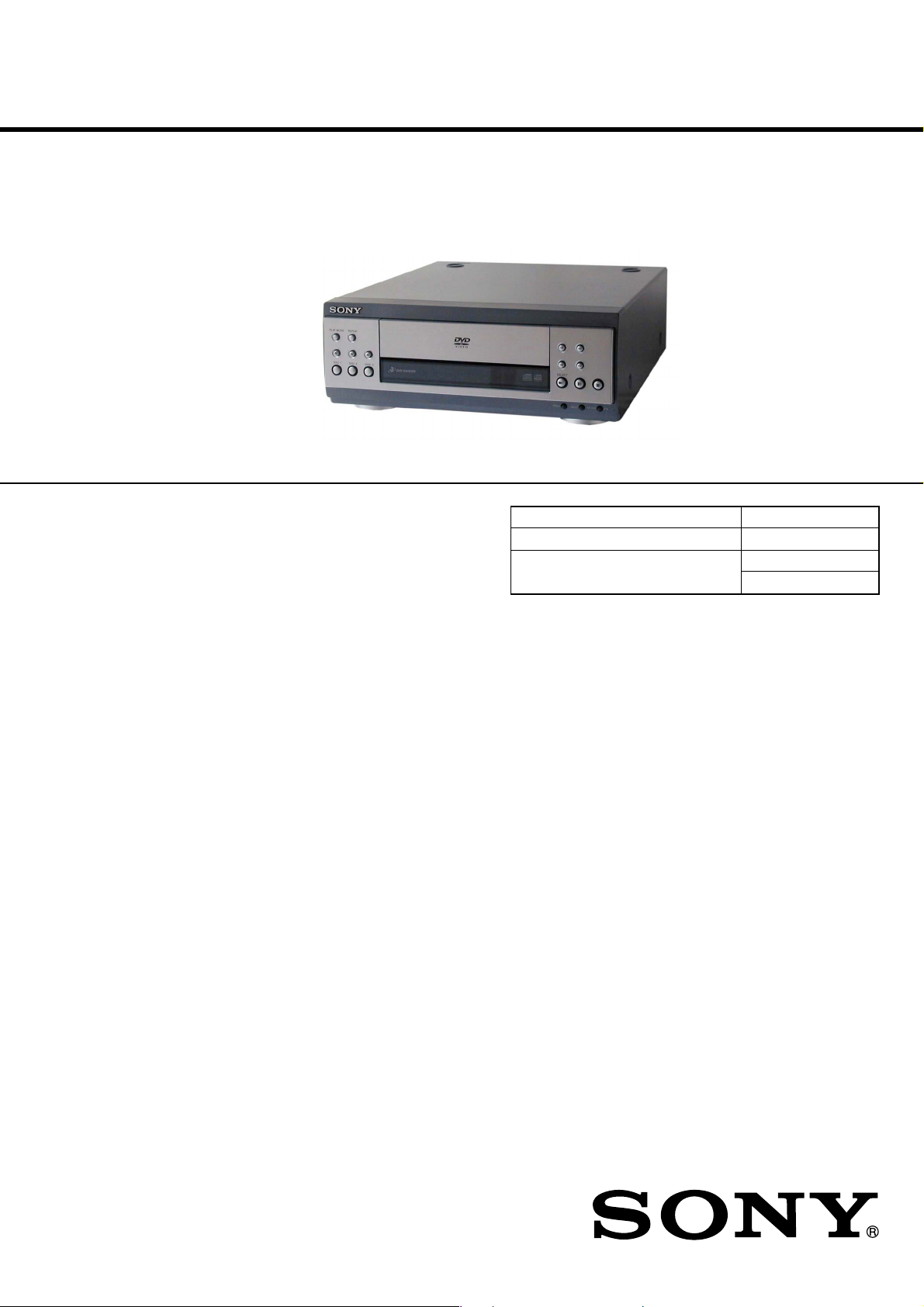
DVP-S90D
SERVICE MANUAL
Ver 1.1 2004.09
DVP-S90D is the DVD/Video CD/CD
player section in MHC-S90D.
SPECIFICATIONS
E Model
Australian Model
Model Name Using Similar Mechanism DVP-S9
CD Mechanism Type CDM63D
Optical Pick-up Name
KHM-240AAA (TYPE A)
KHM-270AAA (TYPE B)
DVD player section
Laser Semiconductor laser
Frequency response DVD (PCM 48 kHz):
Signal-to-noise ratio More than 90 dB
Dynamic range More than 90 dB
Video color system format NTSC, PAL
OPTICAL OUT
(Square optical connector jack, rear panel)
General
Power requirements
Australian model: 230 – 240 V AC, 50/60 Hz
Saudi Aravia, Singapore, Middle East models
Dimensions (w/h/d) Approx. 280 x 108 x 330 mm
Mass Approx. 2.9 kg
Design and specifications are subject to change without notice.
( λ =650 nm/780 nm)
Emission duration: continuous
2 Hz – 22 kHz = (±1 dB)
CD: 2Hz – 20 kHz = (±1 dB)
120 V, 220 V or 230 – 240 V AC,
50/60 Hz
Adjustable with voltage selector
9-877-289-02 Sony Corporation
2004I02-1 Audio Group
C 2004.09 Published by Sony Engineering Corporation
DVD/VIDEO CD/CD PLAYER
Page 2
DVP-S90D
Ver 1.1
CAUTION
Use of controls or adjustments or performance of procedures
other than those specified herein may result in hazardous radiation exposure.
This appliance is
classified as a CLASS 1
LASER product. The
CLASS 1 LASER
PRODUCT MARKING
is located on the rear
exterior.
CAUTION
The use of optical instruments with this product will
increase eye hazard.
As the laser beam used in this CD/DVD Player is
harmful to eyes, do not attempt to disassemble the
cabinet. Refer servicing to qualified personnel only.
The following caution label is located inside the
apparatus.
NOTES ON HANDLING THE OPTICAL PICK-UP
BLOCK OR BASE UNIT
The laser diode in the optical pick-up block may suffer electrostatic break-down because of the potential difference generated
by the charged electrostatic load, etc. on clothing and the human
body.
During repair, pay attention to electrostatic break-down and also
use the procedure in the printed matter which is included in the
repair parts.
The flexible board is easily damaged and should be handled with
care.
NOTES ON LASER DIODE EMISSION CHECK
The laser beam on this model is concentrated so as to be focused
on the disc reflective surface by the objective lens in the optical
pick-up block. Therefore, when checking the laser diode emission, observe from more than 30 cm away from the objective lens.
Notes on chip component replacement
• Never reuse a disconnected chip component.
• Notice that the minus side of a tantalum capacitor may be damaged by heat.
Flexible Circuit Board Repairing
• Keep the temperature of the soldering iron around 270 ˚C during repairing.
• Do not touch the soldering iron on the same conductor of the
circuit board. (within 3 times)
• Be careful not to apply force on the conductor when soldering
or unsoldering.
NOTES ON MB BOARD EXCHANGE
If a MB board is exchanged, “DRIVE AUTO ADJUSTMENT’’
may be unable to be performed. In this case, initialize a memory
in the following procedure.
1. Starting Test Mode (See page 11).
2. Press the 2 button of remote commander to set the Drive
Manual Operation (See page 18).
3. Press the 6 button of remote commander to set the Memory
Check (See page 20).
4. Press the [CLEAR] button of remote commander to initialize a
memory.
SAFETY-RELATED COMPONENT WARNING!!
COMPONENTS IDENTIFIED BY MARK 0 OR DOTTED
LINE WITH MARK 0 ON THE SCHEMATIC DIAGRAMS
AND IN THE PARTS LIST ARE CRITICAL TO SAFE
OPERATION. REPLACE THESE COMPONENTS WITH
SONY PARTS WHOSE PART NUMBERS APPEAR AS
SHOWN IN THIS MANUAL OR IN SUPPLEMENTS PUBLISHED BY SONY.
2
Page 3
DVP-S90D
C016
C022
e
Ver 1.1
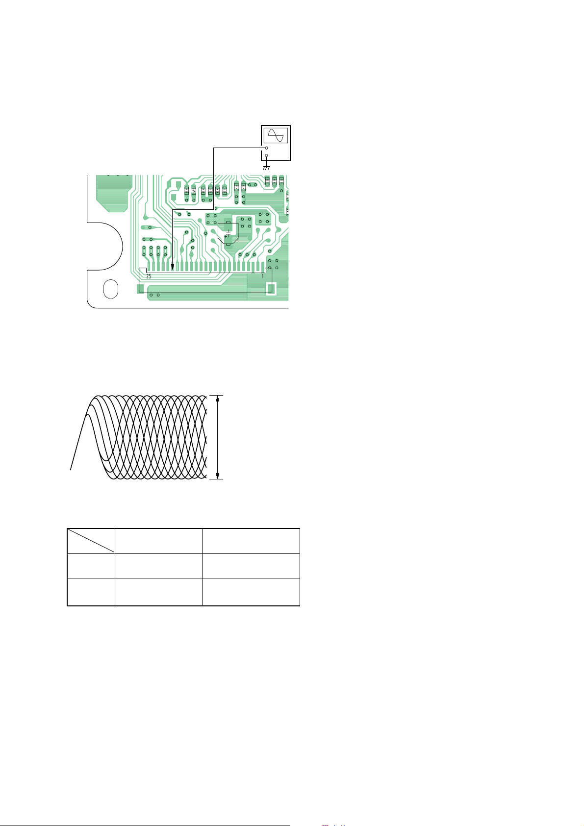
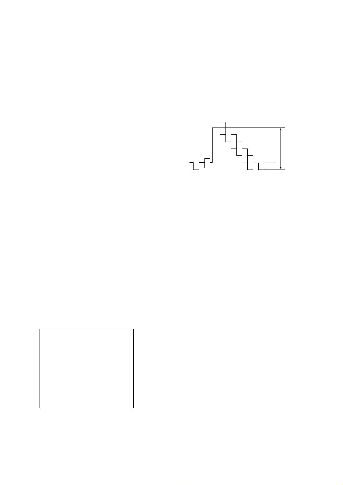
RFMON Level Check
Perform a RFMON level check before exchanging optical pick-up.
Connection:
oscilloscop
CN002 (20pin)
+
–
–RF board (COMPONENT SIDE) –
C028
R037
C035
C033
CN002
C032
C027
C031
C044
VOLT/DIV: 200 mV
TIME/DIV: 500 ns
RFMON level
C025
C015
R0
C039
20
RFMON signal waveform
• Standard value
RFMON level
Standard Value
1.09±0.2Vp-p
1.05±0.2Vp-p
DVD
CD
Test Disc
TDV-520CSO
(J-2501-236-A)
LUV-PO1
(4-999-032-01)
TABLE OF CONTENTS
1. SERVICING NOTES ............................................... 4
2. GENERAL ................................................................... 5
3. DISASSEMBLY
3-1. Disassembly Flow ........................................................... 6
3-2. Cover ............................................................................... 7
3-3. CD Mechanism Deck (CDM63D) .................................. 7
3-4. MB Board ........................................................................ 8
3-5. VIDEO Board.................................................................. 8
3-6. MAIN Board ................................................................... 9
3-7. Front Panel Section ......................................................... 9
3-8. PANEL Board, SUB PANEL Board ............................... 10
3-9. Lid (CD) .......................................................................... 10
4. TEST MODE .............................................................. 11
5. ELECTRICAL ADJUSTMENTS ......................... 22
6. DIAGRAMS
6-1. Block Diagram – RF/SERVO Section – ........................ 23
6-2. Block Diagram – MAIN Section (1/2) – ....................... 24
6-3. Block Diagram – MAIN Section (2/2) – ....................... 25
6-4. Block Diagram
– INTERFACE CONTROL Section – ............................ 26
6-5. Note For Printed Wiring Boards
and Schematic Diagrams ................................................ 27
6-6. Printed Wiring Board – RF Board – .............................. 28
6-7. Schematic Diagram – RF Board – ................................. 29
6-8. Printed Wiring Boards – DISC SENSOR/DRIVER/
IN OUT SW/MOTOR/TRAY SENSOR Boards – ......... 30
6-9. Schematic Diagram – DISC SENSOR/DRIVER/
IN OUT SW/MOTOR/TRAY SENSOR Boards – ......... 31
6-10. Printed Wiring Board
– MB Board (Component Side) – ................................... 32
6-11. Printed Wiring Board
– MB Board (Conductor Side) –..................................... 33
6-12. Schematic Diagram – MB Board (1/6) –....................... 34
6-13. Schematic Diagram – MB Board (2/6) –....................... 35
6-14. Schematic Diagram – MB Board (3/6) –....................... 36
6-15. Schematic Diagram – MB Board (4/6) –....................... 37
6-16. Schematic Diagram – MB Board (5/6) –....................... 38
6-17. Schematic Diagram – MB Board (6/6) –....................... 39
6-18. Printed Wiring Board – MAIN Board – ........................ 40
6-19. Schematic Diagram – MAIN Board – ........................... 41
6-20. Printed Wiring Boards
– PANEL/SUB PANEL/VIDEO Boards – ..................... 42
6-21. Schematic Diagram
– PANEL/SUB PANEL/VIDEO Boards – ..................... 43
6-22. IC Pin Function Description ........................................... 47
7. EXPLODED VIEWS
7-1. Case Section .................................................................... 57
7-2. Front Panel Section ......................................................... 58
7-3. Chassis Section ............................................................... 59
7-4. CD Mechanism Deck Section-1 (CDM63D) ................. 60
7-5. CD Mechanism Deck Section-2 (CDM63D) ................. 61
7-6. CD Mechanism Deck Section-3 (CDM63D) ................. 62
7-7. CD Mechanism Deck Section-4 (CDM63D) ................. 63
7-8. Optical Pick-up Section .................................................. 64
8. ELECTRICAL PARTS LIST ............................... 65
3
Page 4
DVP-S90D
k
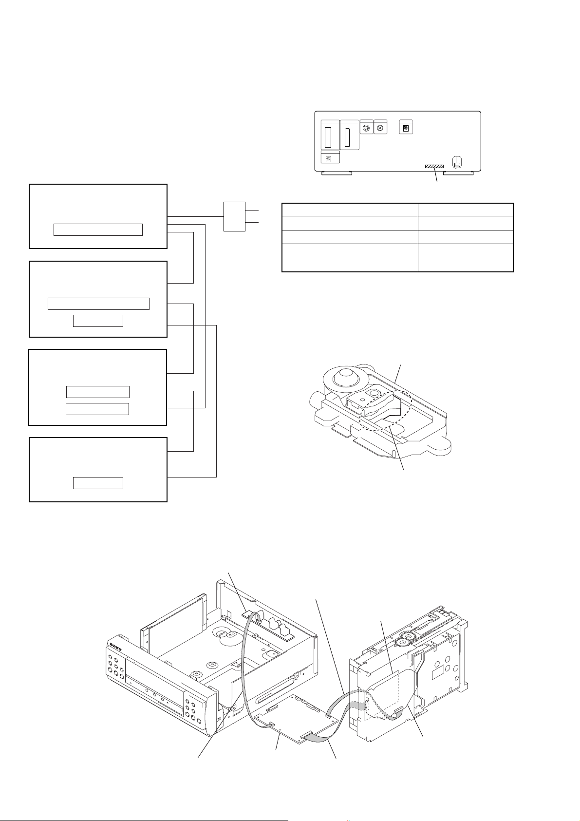
SECTION 1
SERVICING NOTES
This set is a component of the MHC-S90D.
The MHC-S90D system configuration is as shown below, and
therefore it does not operate normally unless all four components
are connected.
In performing the repair, connect all components with the system
cables.
Note: The precaution to the users is described on the label stuck on the
back panel (DVD/video CD/CD player) and in the troubleshooting
section in the Operation Manual.
System Configuration:
AC IN
TA
POWER SUPPLY
ST
MASTER & GRAPHIC µcon
DISPLAY
MODEL IDENTIFICATION
- Back Panel -
PART N o .
Model PART No.
Singapore model 4-244-851-0
E15 model 4-244-851-1
Austrarian model 4-244-851-2
Saudi Arabia model 4-244-851-4
•Abbreviation
E15 : 220 – 240 V AC Area in E model
TYPE A/B DISCRIMINATION
[]
[]
[]
[]
optical device
DVP
HTC & MB µcon
POWER BLOCK
TC
TC µcon
SERVICE POSITION
In checking the CD block and another board, prepare jigs (extension cable J-2501-155-A: 300 mm 9 cores, J-2501-199-A: 300 mm 25
cores, J-2501-202-A: 300 mm 8 cores).
VIDEO board
Connect jig (extension cable J-2501-155-A)
to the MB board (CN015) and optical pick-up block.
SILVER: KHM-240AAA (TYPE A)
BLACK: KHM-270AAA (TYPE B)
RF board
optical pick-up bloc
Connect jig (extension cable J-2501-202-A)
to the MB board (CN012) and VIDEO board (CN201).
MB board
Connect jig (extension cable J-2501-199-A)
to the MB board (CN010) and RF board (CN002).
4
Page 5
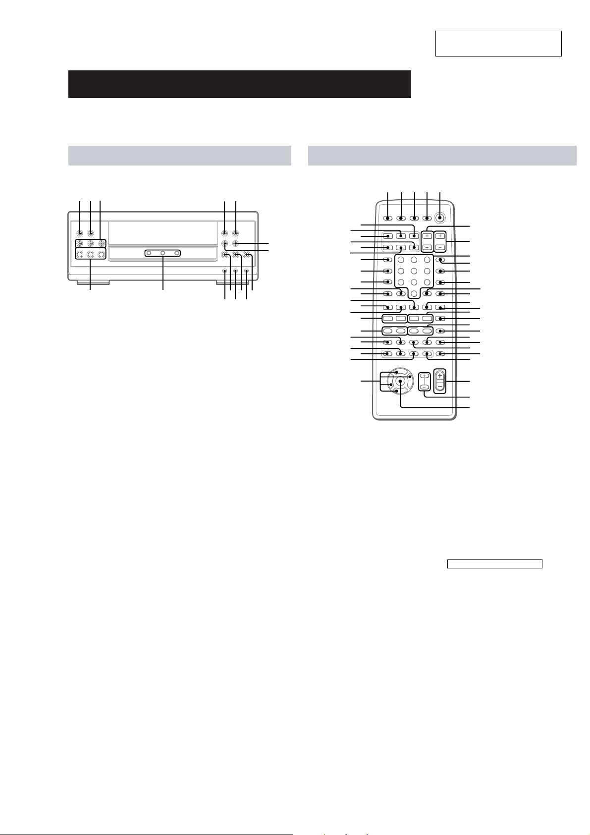
Parts Identification
ANGLE es
AUDIO ws
CLEAR qs
CLOCK/TIMER SELECT 3
CLOCK/TIMER SET 2
DBFB ra
D.SKIP 9
DIGITAL rf
DISPLAY rj
DVD DISPLAY wd
DVD MENU wa
DVD SET UP ql
ENTER wj
EQ ea
EQ ON/OFF wl
FILE SELECT +/– wh
FUNCTION rd
GROOVE rs
KARAOKE PON (Except for
North American and European
models) el
MD rh
Numeric buttons 8
PLAY MODE qa
REPEAT q;
RETURN O qd
SELECT DVD N eh
SET UP wf
SLEEP 1
SLOW t/T qk
SPECTRUM ANALYZER rk
STEP c/C ef
SUBTITLE ed
SUR e;
TAPE A nN ek
TAPE B nN qf
TITLE w;
TUNER/BAND ej
TV @/1 4
TV CH +/– 7
TV/VIDEO rl
TV VOL +/– 6
VIDEO rg
VOL +/– wg
x
Mm>.
nN
O
X
TtCc
V
v
Bb
1234 5
e;
es
ef
ej
eg
6
7
9
8
q;
qa
qd
qs
qf
qg
qj
qh
qk
ql
wa
wd
ws
wf
w;
wg
wj
wh
wk
ed
wl
ea
eh
el
rs
ra
rd
ek
r;
rg
rj
rl
rf
rh
rk
BUTTON DESCRIPTIONS
@/1 (power) 5
X (pause) qj
x (stop) qg
m/M (rewind/fast forward),
TUNING –/+ qh
./> (go backward/
go forward), PRESET –/+,
PREV/NEXT eg
O/o/P/p wk
>10 r;
The items are arranged in alphabetical order.
Refer to the pages indicated in parentheses ( ) for details.
SECTION 2
GENERAL
DVP-S90D
This section is extracted from
instruction manual.
Main unit
DVD/VIDEO CD/CD player
wl e;ea es
1 2 3
rd
DISC 1–3 rd
DISC 1–3 indicators rs
DISC 1–3 Z (eject) ea
NEXT el
PLAY MODE wl
PREV ra
REPEAT e;
RETURN O ej
N SELECT (play) r;
X (pause) ek
x (stop) eh
. (go backward) eg
> (go forward) ef
m (rewind) es
M (fast forward) ed
ed
mM
>
.
HS x
ehekr;rs
ejelra
Remote control
ef
eg
5
Page 6
DVP-S90D
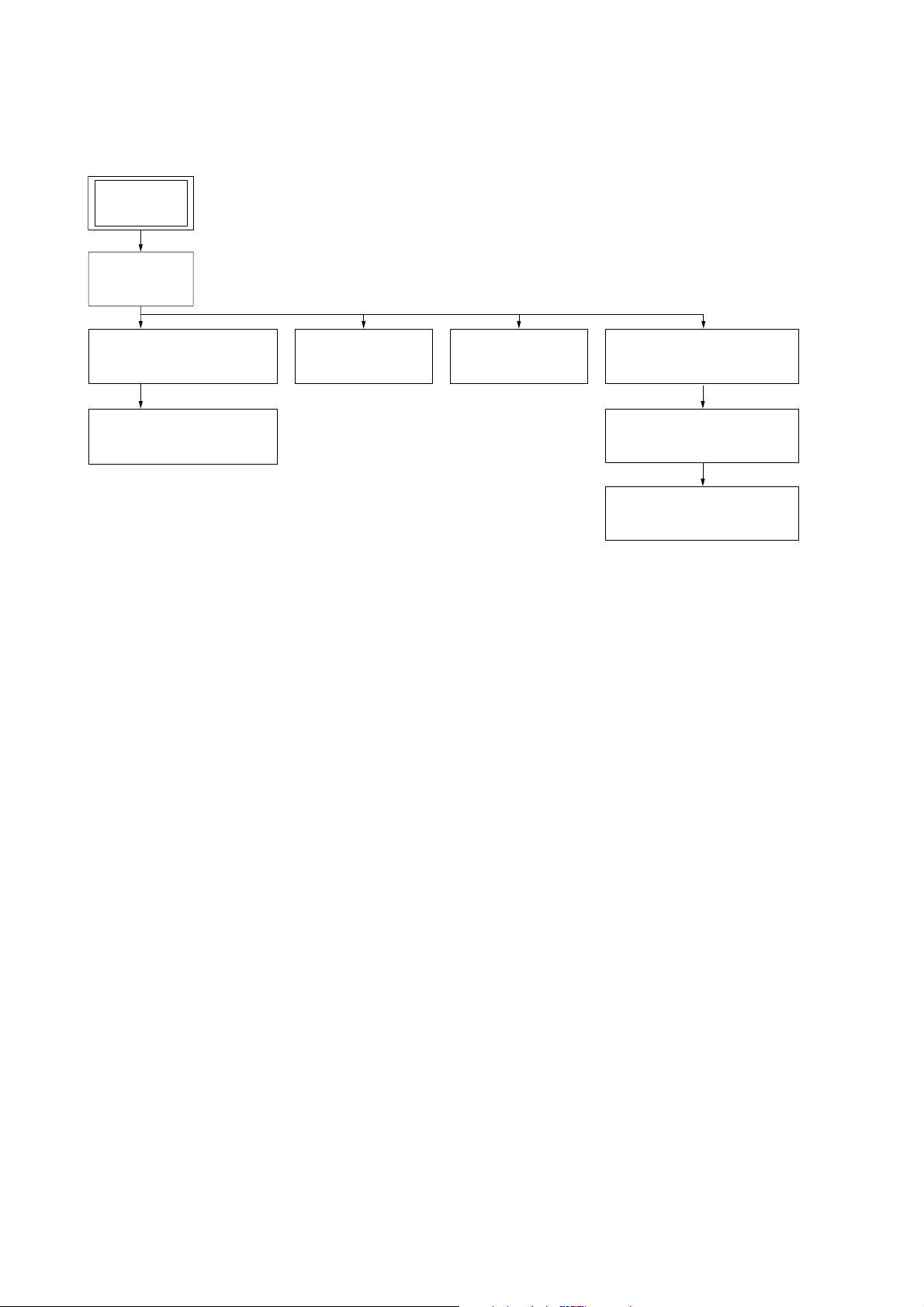
• This set can be disassembled in the order shown below.
3-1. DISASSEMBLY FLOW
SET
3-2. COVER
(Page 7)
SECTION 3
DISASSEMBLY
3-3. CD MECHANISM DECK
(CDM63D)
(Page 7)
3-4. MB BOARD
(Page 8)
3-5. VIDEO BOARD
(Page 8)
3-6. MAIN BOARD
(Page 9)
3-7. FRONT PANEL SECTION
(Page 9)
3-8. PANEL BOARD,
SUB PANEL BOARD
(Page 10)
3-9. LID (CD)
(Page 10)
6
Page 7
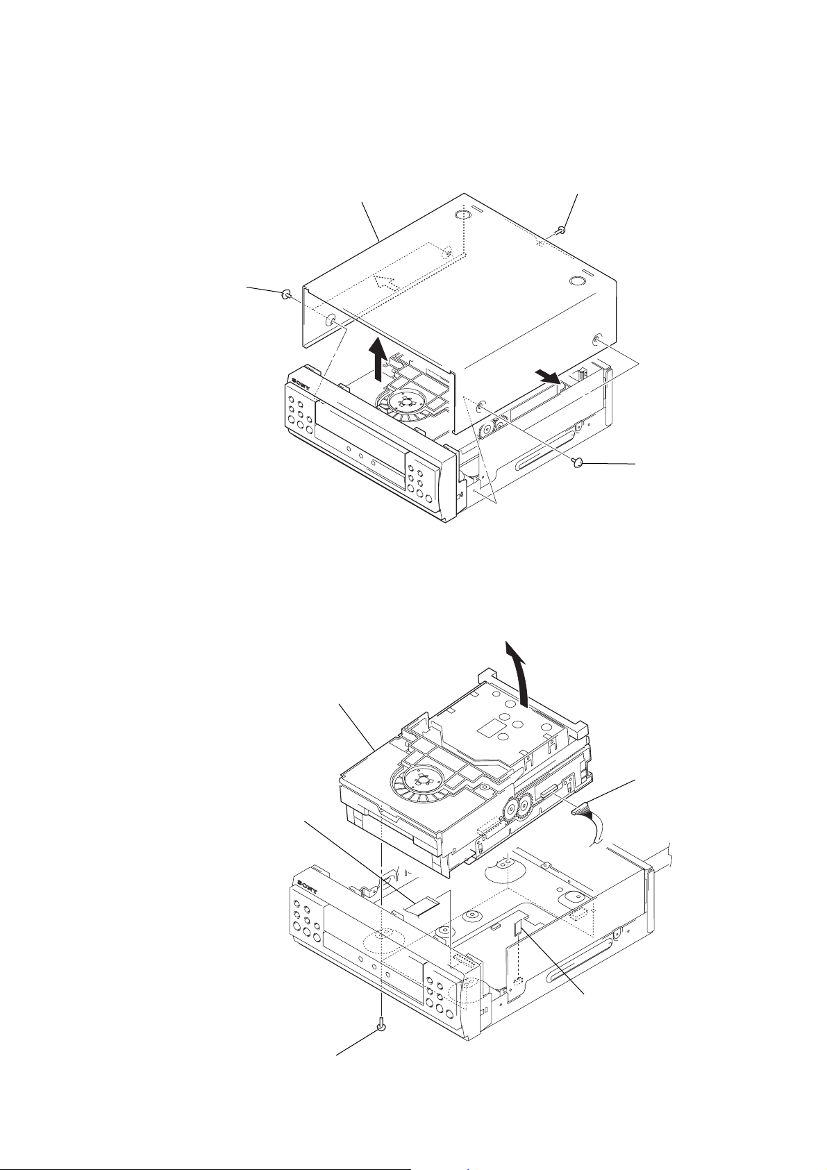
Note: Follow the disassembly procedure in the numerical order given.
)
3-2. COVER
3
Cover
1
Tw o screws
(Case 3 TP2)
2
Screw
(BVTT3 × 6)
DVP-S90D
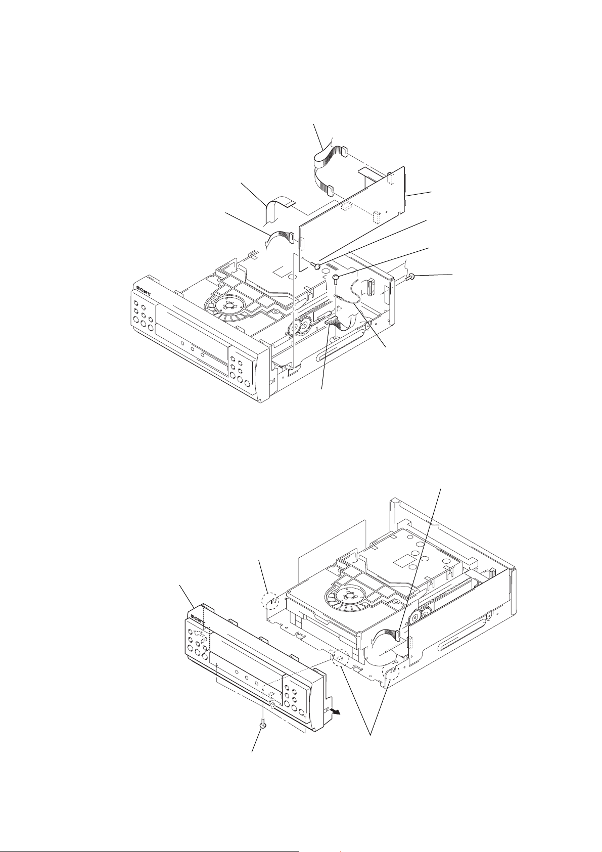
3-3. CD MECHANISM DECK (CDM63D)
4
CD mechanism deck (CDM63D)
5
Wire (flat type) (25 core)
(CN010)
1
Tw o screws
(Case 3 TP2)
2
Connector
(CN701)
3
Four screws
(BVTP3
1
Wire (flat type) (9 core
(CN015)
×
8)
7
Page 8
DVP-S90D
r
s
3-4. MB BOARD
2
1
4
Tw o screws
(BV)
Wire (flat type) (25 core)
(CN010)
Wire (flat type) (8 core)
(CN011)
1
Wire (flat type) (9 core)
(CN015)
4
Tw o screws
(BV)
6
MB board
5
Lug
3
Connecto
(CN008)
3-5. VIDEO BOARD
4
VIDEO board
2
Connector
(CN202)
1
Wire (flat type) (8 core)
3
Three screw
(BVTP3 × 8)
8
Page 9
3-6. MAIN BOARD
)
1
Wire (flat type) (10 core)
(CN107)
2
Connector
(CN401)
3
Tw o connectors
(CN101, 102)
9
MAIN board
7
Screw
(BVTP3 × 8)
5
Screw
(BVTP3 × 8)
8
Screw
(BVTP3
DVP-S90D
×
8
3-7. FRONT PANEL SECTION
4
Front panel section
3
Claw
4
Connector
(CN701)
6
Lug
1
Connector
(CN401)
2
Three screws
(BVTP3
3
Tw o claws
×
8)
9
Page 10
DVP-S90D
d
)
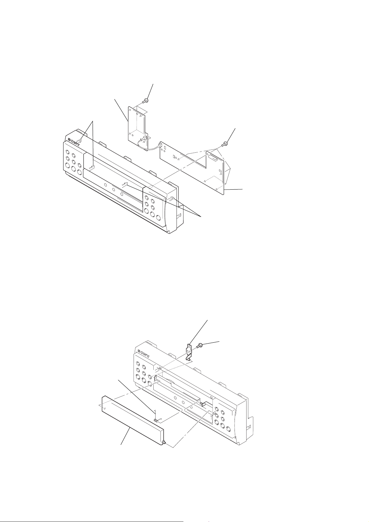
3-8. PANEL BOARD, SUB PANEL BOARD
6
SUB PANEL board
5
Tw o claws
4
Four screws
(BVTP2.6
×
8)
1
Five screws
(BVTP2.6
3
×
8)
PANEL boar
3-9. LID (CD)
4
Spring (CD)
2
Tw o claws
2
Bracket (LID) assy
1
Screw
(BVTP2.6 × 8
10
3
Lid (CD)
Page 11

SECTION 4
TEST MODE
DVP-S90D
Note: Use following buttons in the test mode.
no mark : Button of DVD/video CD/CD player (DVP-S90D)
*1 : Button of A/V amplifier (TA-S90D)
*2 : Button of tuner (ST-S90D)
[CHANGE-OVER THE COLOR SYSTEM]
• The color system can be changed over NTSC or PAL.
Procedure:
1. Press the I/1 *1 button to turn the power on.
2. Turn the [FUNCTION]*
1
knob to select “DVD”, and press
the x button.
3. While pressing the both [RETURN] and [REPEAT] buttons,
turn the power off.
4. Press the I/1 *1 button to turn the power on. The color sys-
tem is changed over.
[COLD RESET]
• The cold reset clears all data including preset data stored in the
RAM to initial conditions. Execute this mode when returning
the set to the customer.
Procedure 1:
1. Press the I/1 *1 button to turn the power on.
2. While pressing the both [PLAY MODE] and x buttons, press
the M button.
3. The set is reset, and becomes standby state.
Procedure 2:
1. Press the I/1 *1 button to turn the power on.
2. While pressing the [DIGITAL]*1 button, press the [DISPLAY]*
button.
3. The set is reset, and becomes standby state.
[DVD DELIVERY MODE]
• This mode moves the optical pick-up to the position durable to
vibration. Use this mode when returning the set to the customer
after repair.
Procedure:
1. Press the I/1 *1 button to turn the power on.
2. Turn the [FUNCTION]*1 knob to select “DVD”.
3. While pressing the [EQ ON/OFF]*1 button, press the I/1 *
button.
4. The message “LOCK” is displayed on the fluorescent indica-
tor tube of tuner unit and turn the power off automatically, and
the DVD delivery mode is set.
[GC TEST MODE]
Enter the GC Test Mode
Procedure 1:
1. Press the I/1 *1 button to turn the power on.
2. While pressing the both [PLAY MODE] and x buttons, press
the Z (DISC 1) button.
3. LEDs and fluorescent indicator tube are all turned on of all
units.
Procedure 2:
1. Press the I/1 *1 button to turn the power on.
2. While pressing the both [STEREO/MONO]*2 and
[CINEMA STUDIO C]*
button.
3. LEDs and fluorescent indicator tube are all turned on of all
units.
1
buttons, press the [CLOCK/TIMER]*
Version Display Mode
Procedure:
1. Enter the GC test mode.
2. Each time the [DISC 1] or [TUNER MEMORY]*2 button is
pressed, microcomputer or mechanism deck version is displayed of each unit.
3. Press the [DISC 3] or [TUNING +]*2 button to detail is dis-
played the version.
Key Check Mode
Procedure:
1. Enter the GC test mode.
2. Press the [DISC 2] or [TUNING --]*2 button to set the key check
mode, and displays “K 0 J 0 V 0” on the fluorescent indicator
tube of tuner unit.
3. All buttons are pressed of video CD unit, all LEDs are blinking of video CD unit. (not change the display of fluorescent
indicator tube)
Releasing the GC Test Mode
To release from this mode, press three buttons in the same manner
as entering this mode or disconnect the power cord.
[DVD SERVICE MODE]
• This mode can run the DVD sled motor optionally. Use this
mode, for instance, when cleaning the optical pick-up.
Procedure:
1. Press the I/1 *1 button to turn the power on.
2
2. Turn the [FUNCTION]*1 knob to select “DVD”.
3. While pressing the both [PLAY MODE] and x buttons, press
the . button.
4. Set to the DVD service mode.
5. With the DVD in stop status, press the M button to move
the optical pick-up to outside track, or press the m button
to inside track.
6. To release from this mode, perform as follows.
1) Move the optical pick-up to the most inside track.
2) Disconnect the power cord.
Notes: • Always move the optical pick-up to most inside track when
1
releasing from this mode. Otherwise, a disc will not be unloaded.
• Do not run the sled motor excessively, otherwise the gear can
be chipped.
[DVD CANCELLATION MODE OF REPEAT LIMITATION]
• This mode can cancel the DVD repeat limitation (5 times).
Procedure:
1. Press the I/1 *1 button to turn the power on.
2. Turn the [FUNCTION]*1 knob to select “DVD”.
3. While pressing the both [PLAY MODE] and x buttons, press
the [REPEAT] button.
4. DVD repeat limitation is canceled.
5. To release this mode, disconnect the power cord.
[DVD DISC TRAY LOCK MODE FOR BURGLARY
PREVENTION]
2
Procedure:
1. Press the I/1 *1 button to turn the power on.
2. Turn the [FUNCTION]*1 knob to select “DVD”.
3. While pressing the both [PLAY MODE] and x buttons, press
the m button, turn the power off.
11
Page 12

DVP-S90D
[GENERAL DESCRIPTION]
The Test Mode allows you to make diagnosis and adjustment easily using the remote commander and monitor TV. The instructions,
diagnostic results, etc. are given on the on-screen display (OSD).
[STARTING TEST MODE]
1. Press the I/1 *1 button to turn the power on.
2. Turn the [FUNCTION]*2 knob to select “DVD”.
3. While pressing the x and [PLAY MODE] button, press
the . button to enter the test mode.
4. It displays “TEST MODE” on the fluorescent indicator tube,
and displays the Test Mode Menu on the monitor screen as
follows. (At the bottom of the menu screen, the model name
and revision number are displayed)
Test Mode Menu
0. Syscon Diagnosis
1. Drive Auto Adjustment
2. Drive Manual Operation
3. Mecha Aging
4. Emergency History
5. Version Information
6. Video Level Adjustment
Exit: POWER Key
_
Model : xxx-xxxx_xx
Revision: 1.xxx
5. To execute each function, select the desired menu and press its
number on the remote commander (RM-SD390AV or RMSD395AV).
6. To release from test mode, press the I/1 *1 button and turn
the power off.
1. All
All items continuous check
This menu checks all diagnostic items continuously. Normally, all
items are checked successively one after another automatically unless an error is found, but at a certain item that requires judgment
through a visual check to the result, the following screen is displayed for the key entry.
### Syscon Diagnosis ###
Diag All Check
No. 2 Version
2-3. ROM Check Sum
Check Sum = 2005
Press NEXT Key to Continue
Press PREV Key to Repeat
_
For the ROM Check, the check sum calculated by the Syscon is
output, and therefore you must compare it with the specified value
for confirmation.
Following the message, press > key to go to the next item,
or . key to repeat the same check again. To quit the diagnosis
and return to the Check Menu screen, press x or [ENTER] key.
If an error occurred, the diagnosis is suspended and the error code
is displayed as shown below.
### Syscon Diagnosis ###
[SYSCON DIAGNOSIS]
The same contents as board detail check by serial interface can be
checked from the remote commander.
On the Test Mode Menu screen, press [10/0] key on the remote
commander, and the following check menu will be displayed.
### Syscon Diagnosis ###
Check Menu
0. Quit
1. All
2. Version
3. Peripheral
4. Servo
5. Supply
6. AV Decoder
7. Video
8. Audio
_
0. Quit
Quit the Syscon Diagnosis and return to the Test Mode Menu.
3-3. EEPROM Check
Error 03: EEPROM Write/Reed N
Address : 00000001
Write Data : 2492
Read Data : 2490
Press NEXT Key to Continue
Press PREV Key to Repeat
_
Press x key to quit the diagnosis, or > key to repeat the same
item where an error occurred, or . key to continue the check
from the item next to faulty item.
12
Page 13

DVP-S90D
Selecting 2 and subsequent items calls the submenu screen of each
item.
For example, if “5. Supply” is selected, the following submenu
will be displayed.
### Syscon Diagnosis ###
Check Menu
No. 5 Supply
0. Quit
1. All
2. ARP Register Check
3. ARP to RAM Data Bus
4. ARP to RAM Address Bus
5. ARP RAM Check
_
0. Quit
Quit the submenu and return to the main menu.
1. All
All submenu items continuous check
This menu checks 2 and subsequent items successively. At the item
where visual check is required for judgment or an error occurred,
the checking is suspended and the message is output for key entry.
Normally, all items are checked successively one after another automatically unless an error is found.
Selecting 2 and subsequent items executes respective menus and
outputs the results.
For the contents of each submenu, see “Check Items List”.
General Description of Checking Method
2. Version
(2-2) Revision
ROM revision number is displayed.Error: Not detected.
The revision number defined in the source file of ROM (At
the beginning of mass production, the Flash ROM of IC107
is used) is displayed with four digits.
(2-3) ROM Check Sum
Check sum is calculated.
Error: Not detected.
The 8-bit data are added at addresses 0x000F0000 ~
0x002EFFFF of ROM (IC107) and the result is displayed
with 4-digit hexadecimal number. Error is not detected.
Compare the result with the specified value.
(2-4) Model Type
Model code is displayed.
Error: Not detected.
The model code read from EEPROM (IC101) is displayed
with 2-digit hexadecimal number.
(2-5) Region
Region code is displayed.
Error: Not detected.
The region code determined from the model code is displayed.
3. Peripheral
(3-2) EEPROM Check
Data write → read, and accord check
Error 03: EEPROM write/read discord
Data 0x9249, 0x2942, 0x4294 are written to addresses
0x00~0xFF of EEPROM (IC101), then read and checked.
Before writing, the data are saved, then after checking, they
are written to restore the contents of EEPROM.
4. Servo
(4-2) Servo DSP Check
Data write → read, and accord check
Error 12: Read data discord
Data 0x9249, 0x2942, 0x4294 are written to the address
0x602 of RAM in the Servo DSP (IC302), then read and
checked.
(4-3) DSP Driver Test
Test signal data → DSP Driver
Error: Not detected.
Caution: Do not conduct this test with a mechanical deck
connected.
The maximum voltage is applied to the Servo Driver IC
(IC401). If mechanical deck is connected, the motor and
optics could be damaged. Disconnect mechanical deck following the output message, then enter specified 4- or 5digit number from the remote commander, and press the
[ENTER]. The test is conducted only when the input data
accord. Check the output level, then press the > to finish the test.
This test is skipped if “All” is selected.
Supplement: How to disconnect mechanical deck
Disconnect flat cables connected to the CN010 and CN015
of MB board. Also, disconnect harness from the CN203.
13
Page 14

DVP-S90D
5. Supply
Caution: Do not conduct this check with a mechanical deck con-
nected.
An access is made to the stream supply and servo control
IC (IC302) and external RAM (IC303) using check data.
If mechanical deck is connected, the motor and optics
could be damaged. This check is also executed by the
“All” menu item.
Supplement: How to disconnect mechanical deck
Disconnect flat cables connected to the CN010 and
CN015 of MB board. Also, disconnect harness from
the CN203.
(5-2) ARP Register Check
Data write → read, and accord check
Error 08: ARP register write, and read data discord
Data 0x00 to 0xFF are written to the TMAX register (address 0xC6) in ARP (IC302), then they are read and checked.
(5-3) ARP to RAM Data Bus
Data write → read, and accord check
Error 09: ARP ←→ RAM data bus error
Data 0x0001 to 0x8000 where one bit each is set to 1 are
written to the address 0 of RAM (IC303) connected to the
ARP (IC302) through the bus, then they are read and
checked. In case of discord, written bit pattern and read
data are displayed. If data where multiple bits are 1 are
read, the bits concerned may touch each other. Further, if
data where certain bit is always 1 or 0 regardless of written
data, the line could be disconnected or shorted.
(5-4) ARP to RAM Address Bus
Data write → other address read discord check
Error 10: ARP → RAM address bus error
Caution: Address and data display in case of an error is
different from the display of other diagnosis (de-
scribed later).
Before starting the test, all addresses of RAM (IC303) are
cleared to 0x0000.
First, 0xA55A is written to the address 0x00000, and the
address data are read and checked from addresses 0x00001
to 0x80000 while shifting 1 bit each. Next, the data at that
address is cleared, and it is written to the address 0x00001,
and read and checked in the same manner. This check is
repeated up to the address 0x80000 while shifting the address data by 1 bit each.
If data other than 0 is read at the addresses except written
address, an error is given because all addresses were already cleared to 0. In this check, the error display pattern is
different from that of other diagnosis; read data, written
address, and read address are displayed in this order. However, the message uses same template, and accordingly exchange Address and Data when reading. The following display, for example,
### Syscon Diagnosis ###
5-4. ARP to RAM Address Bus
Error 10: ARP - RAM Address B
Address : 0000A55A
Write Data : 00000000
Read Data : 00080000
Press NEXT Key to Continue
Press PREV Key to Repeat
_
shows the data 0xA55A was read from address 0x00080000
though it was written to the address 0x00000000. This implies that these addresses are in the form of shadow. Also,
if the read data is not 0xA55A, another error will be present.
(5-5) ARP RAM Check
Data write → read, and accord check
Error 11: ARP RAM read data discord
The program code data stored in ROM are copied to all
areas of RAM (IC303) connected to the ARP (IC302)
through the bus, then they are read and checked if they accord. If the detail check was selected initially, the data are
written to all areas and read, then the same test is conducted
once again with the data where all bits are inverted between
1 and 0. If discord is detected, faulty address, written data,
and read data are displayed following the error code 11,
and the test is suspended.
14
Page 15

DVP-S90D
6. AV Decoder
(6-2) 1930 RAM
Data write → read, and accord check
Error 13: AVD RAM read data discord
The program code data stored in ROM (IC107) are copied
to all areas oo»RAM (IC504, IC505) connected to the AVD
(IC503) through the bus, then they are read and checked if
they accord. Further, the same test is conducted once again
with the data where all bits are inverted between 1 and 0. If
discord is detected, faulty address, written data, and read
data are displayed following the error code 13, and the test
is suspended.
(6-3) 1930 SP
ROM → AVD RAM → Video OUT
Error: Not detected.
The data including sub picture streams in ROM (IC107)
are transferred to the RAM (IC504, IC505) in AVD (IC503),
and output as video signals from the AVD (IC503).
They are output from all video terminals (Composite, Y/C).
7. Video
(7-2) Color Bar
AVD color bar command write → Video OUT
Error: Not detected.
The command is transferred to the AVD, and the color bar
signals are output from video terminals.
They are output from all video terminals (Composite, Y/C).
Check Items List
2) Version
(2-2) Revision
(2-3) ROM Check Sum
(2-4) Model Type
(2-5) Region
3) Peripheral
(3-2) EEPROM Check
4) Servo
(4-2) Servo DSP Check
(4-3) DSP Driver Test
5) Supply
(5-2) ARP Register Check
(5-3) ARP to RAM Data Bus
(5-4) ARP to RAM Address Bus
(5-5) ARP RAM Check
6) AV Decoder
(6-2) 1930 RAM
(6-3) 1930 SP
7) Video
(7-2) Color Bar
(7-3) Composit Out
(7-4) Y/C Out
(7-6) Component Out
(7-3) Composit Out
(7-4) Y/C Out
(7-6) Component Out
8. Audio
(8-2) ARP → 1930
Error 14 : ARP → 1930 video NG
15 : ARP → 1930 audio NG
(8-3) Test Tone
All channels
2ch Left
2ch Right
Front Left
Front Right
Rear Left
Rear Right
Center
Sub Woofer
8) Audio
(8-2) ARP → 1930
(8-3) Test Tone
Error Codes List
00: Error not detected
01: RAM write/read data discord
02: Gate array NG
03: EEPROM NG
08: ARP register read data discord
09: ARP ←→ RAM data bus error
10: ARP ←→ RAM address bus error
11: ARP RAM read data discord
12: Servo DSP NG
13: 1930 SDRAM NG
14: ARP → 1930 video NG
15: ARP → 1930 audio NG
16: 1910 UCODE download NG
17: System call error (function not supported)
18: System call error (parameter error)
19: System call error (illegal ID number)
20: System call error (time out)
90: Error occurred
91: User verification NG
92: Diagnosis cancelled
15
Page 16

DVP-S90D
[DRIVE AUTO ADJUSTMENT]
On the Test Mode Menu screen, press [1] key on the remote commander, and the drive auto adjustment menu will be displayed.
## Drive Auto Adjustment ##
Adjustment Menu
0. ALL
1. DVD-SL
2. CD
3. DVD-DL
Exit: RETURN
Normally, [10/0] is selected to adjust DVD (single layer), CD and
DVD (dual layer). But, individual items can be adjusted for the
case where adjustment is suspended due to an error. In this mode,
the adjustment can be made easily through the operation following the message displayed on the screen.
The disc used for adjustment must be the one specified for adjustment.
0. ALL
Select [10/0] and press [ENTER] key, and the servo set data in
EEPROM will be initialized. Then, 1. DVD-SL disc, 2. CD disc
and 3. DVD-DL disc are adjusted in this order. Each time one disc
was adjusted, it is ejected. Replace it with the specified disc following the message. You can finish the adjustment if pressing
the x button. During adjustment of each disc, the measurement
for disc type judgment is made. As automatic adjustment does not
judge the disc type unlike conventional models, take care not to
insert wrong type discs. Also, do not give a shock during adjustment.
1. DVD-SL (single layer)
Select [1], insert DVD single layer disc, and press [ENTER] key,
and the adjustment will be made through the following steps, then
adjusted values will be written to the EEPROM.
DVD Single Layer Disc Adjustment Steps
1. SLED TILT Reset
2. Disc Check Memory SL
3. Wait 300 msec
4. Set Disc Type SL
5. LD ON
6. Spdl Start
7. Wait 1 sec
8. Focus Servo ON 0
9. Auto Track Offset Adjust
10. CLVA ON
11. Wait 500 msec
12. Tracking ON
13. Wait 1 sec
14. Sled ON
15. Check CLV Lock
16. Auto LFO Adjust
17. Auto Focus Offset Adjust
18. Auto Tilt Position Adjust
19. Auto Focus Gain Adjust
20. Auto Focus Offset Adjust
21. EQ Boost Adjust
22. Auto LFO Adjust
23. Auto Track Gain Adjust, Search Check
24. 32Tj Fwd
25. 32Tj Rev
26. 500Tj Fwd
27. 500Tj Rev
28. All Servo Stop
29. Eep Copy Loop Filter Offset
16
Page 17

DVP-S90D
2. CD
Select [2], insert CD disc, and press [ENTER] key, and the adjustment will be made through the following steps, then adjusted values will be written to the EEPROM.
CD Adjustment Steps
1. Sled Tilt Rest
2. Disc Check Memory CD
3. Wait 500 msec
4. Set Disc Type CD
5. LD ON
6. Spdl Start
7. Wait 500 msec
8. Focus Servo ON 0
9. Auto Track Offset Adjust
10. CLVA ON
11. Wait 500 msec
12. Tracking ON
13. (TC Display Start)
14. Wait 1 sec
15. Jitter Display Start
16. Sled ON
17. Check CLV ON
18. Auto LFO Adjust
19. Auto Focus Offset Adjust
20.
21. Auto Focus Gain Adjust
22. Auto Focus Offset Adjust
23. Eq Boost Adjust
24. Auto LFO Adjust
25. Auto Track Gain Adjust, Search Check
26. 32Tj Fwd
27. 32Tj Rev
28. 500Tj Fwd
29. 500Tj Rev
30. All Servo Stop
3. DVD-DL (dual layer)
Select [3], insert DVD dual layer disc, and press [ENTER] key,
and the adjustment will be made through the following steps, then
adjusted values will be written to the EEPROM.
DVD Dual Layer Disc Adjustment Steps
1. Sled Tilt Reset
2. Disc Check Memory DL
3. Wait 500 msec
4. Set Disc Type DL
5. LD ON
6. Spdl Start
7. Wait 1 sec, Layer 1 Adjust
8. Focus Servo ON 0
9. Auto Track Offset Adjust
10. Clva ON
11. Wait 500 msec
12. Tracking ON
13. Wait 500 msec
14. Sled ON
15. Check CLV Lock
16. Auto Loop Filter Offset Auto Focus Adjust
17.
18. Auto Focus Gain Adjust
19. Auto Focus Offset Adjust
20. Eq Boost Adjust
21. Auto Loop Filter Offset
22. Auto Track Gain Adjust, Search Check
23. 32Tj Fwd
24. 32Tj Rev
25. 500Tj Fwd
26. 500Tj Rev, Layer 0 Adjust
27. Fj (L1 -> L0)
28. Auto Track Offset Adjust L0
29. Clva ON
30. Wait 500 msec
31. Tracking ON
32. Wait 500 msec
33. Sled ON
34. Check CLV Lock
35. Auto Focus Filter Offset
36. Auto Focus Adjust
37.
38. Auto Focus Gain Adjust
39. Auto Focus Offset Adjust
40. Eq Boost Adjust
41. Auto Loop Filter Offset
42. Auto Track Gain Adjust, Search Check
43. 32Tj Fwd
44. 32Tj Rev
45. 500Tj fwd
46. 500Tj Rev, Layer Jump Check
47. Lj (L0 -> L1)
48. Lj (L1 -> L0)
49. All Servo Stop
17
Page 18
DVP-S90D
[DRIVE MANUAL OPERATION]
On the Test Mode Menu screen, select [2], and the manual operation menu will be displayed. For the manual operation, each servo
on/off control and adjustment can be executed manually.
## Drive Manual Operation ##
Operation Menu
1. Disc type
2. Servo Control
3. Track/Layer Jump
4. Manual Adjustment
5. Auto Adjustment
6. Memory Check
7. Sacd Water Mark
0. Disc Check Memory
_
Exit: Return
In using the manual operation menu, take care of the following
points. These commands do not provide protection, thus requiring
correct operation. The sector address or time code field is displayed when a disc is loaded.
1. Set correctly the disc type to be used on the Disc Type
screen.
The disc type must be set after a disc was loaded.
The set disc type is cleared when the tray is opened.
2. After power ON, if the Drive Manual Operation was selected, first perform “Reset SLED TILT” by opening 1.
Disc Type screen.
3. In case of an alarm, immediately press the x button to
stop the servo operation, and turn the power OFF.
Basic operation (controllable from front panel or remote commander)
I/1 Power OFF
x Servo stop
Z Stop+Eject/Loading
[RETURN] Return to Operation Menu or Test Mode
Menu
> , . Transition between sub modes of menu
[1] to [9], [10/0] Selection of menu items
Cursor ↑ / ↓ Increase/Decrease in manually adjusted
value
0. Disc Check Memory
Disc Check
1. SL Disc Check
2. CD Disc Check
3. DL Disc Check
0. Reset SLED TILT
_
On this screen, the mirror time is measured to judge the disc and it
is written to the EEPROM. First load DVD SL disc and press [1],
next load CD disc and press [2], and finally load DVD DL disc
and press [3].
The adjustment must be executed more than once after default
data were written. External vibration or shock to the player must
not be given. Reference value for DVD is from 10 to 20, and for
CD, from 28 to 4F.
Check that the value of CD is larger than that of DVD.
When those values are beyond a range perform this adjustment
again.
From this screen, you can go to another mode by
pressing > or . key, but you cannot enter this mode from
another mode. You can enter this mode from the Operation Menu
screen only.
1. Disc Type
Disc Type
1. Disc Type Auto Check
2. DVD SL 12 cm
3. DVD DL 12 cm
4. CD 12cm
5. LCD 12 cm
6. DVD SL 8 cm
7. DVD DL 8 cm
8. CD 8 cm
9. LCD 8 cm
0. Reset SLED TILT
-- SA. ------ SI. -- EMG. 00
DVD SL12cm
On this screen, select the disc type. To select the disc type, press
the number of the loaded disc. The selected disc type is displayed
at the bottom. Selecting [1] automatically selects and displays the
disc type. In case of wrong display, retry “Disc Check Memory”.
Also, opening the tray causes the set disc type to be cleared. In
this case, set the disc type again after loading.
In performing manual operation, the disc type must be set.
Once the disc type has been selected, the sector address or time
code display field will appear as shown below. These values are
displayed when PLL is locked.
18
Page 19

DVP-S90D
1. Disc Type Auto Check
Disc Type
2. DVD SL 12 cm
3. DVD DL 12 cm
4. CD 12cm
5. LCD 12 cm
6. DVD SL 8 cm
7. DVD DL 8 cm
8. CD 8 cm
9. LCD 8 cm
0. Reset SLED TILT
SA. SI. EMG. 00
DVD SL 12 cm
Display when DVD SL 12cm disc was selected
Disc Type
1. Disc Type Auto Check
2. DVD SL 12 cm
3. DVD DL 12 cm
4. CD 12cm
5. LCD 12 cm
6. DVD SL 8 cm
7. DVD DL 8 cm
8. CD 8 cm
9. LCD 8 cm
0. Reset SLED TILT
TC. : : EMG. 00
CD 12 cm
2. Servo Control
Servo Control
1. LD Off R.Sled FWD
2. SP Off L.Sled REV
3. Focus Off
4. TRK. Off
5. Sled Off
6. CLVA Off
7. FCS. Srch Off
0. Reset SLED TILT
SA. SI. EMG. 00
DVD SL 12 cm
On this screen, the servo on/off control necessary for replay is
executed. Normally, turn on each servo from 1 sequentially and
when CLVA is turned on, the usual trace mode becomes active. In
the trace mode, DVD sector address or CD time code is displayed.
This is not displayed where the spindle is not locked.
The spindle could run overriding the control if the spindle system
is faulty or RF is not present. In such a case, do not operate CLVA.
[10/0] Reset SLED TILT Reset the Sled
and Tilt to initial position.
[1] LD Turn ON/OFF the laser.
Display when CD 12cm disc was selected
[0] Reset SLED TILT Reset the Sled and Tilt to initial posi-
tion.
[1] Disk Type Check Judge automatically the loaded disc. As
the judged result is displayed at the bottom of screen, make sure that it is correct.
If Disc Check Memory menu has not
been executed after EEPROM default
setting, the disc type cannot be judged.
In this case, return to the initial menu
and make a check for three types of
discs (SL, DL, CD).
[2] to [9] Select the loaded disc. The adjusted
value is written to the address of selected disc. No further entry is necessary if [1] was selected.
[2] SP Turn ON/OFF the spindle.
[3] Focus Search the focus and turn on the focus.
[4] TRK Turn ON/OFF the tracking servo.
[5] Sled Turn ON/OFF the sled servo.
[6] CLVA Turn ON/OFF normal servo of spindle
servo.
[7] FCS. Srch Apply same voltage as that of focus
search to the focus drive to check the
focus drive system.
→ Sled FWD Move the sled outward. Perform this
operation with the tracking servo turned
off.
← Sled REV Move the sled inward. Perform this op-
eration with the tracking servo turned
off.
↑ Tilt UP Move the tilt upward.
↓ Tilt DOWN Move the tilt downward.
The following menus are normally not used.
3. Track/Layer Jump
4. Manual Adjustment
5. Auto Adjustment
The persons who do not know well about these menus should not
use them.
19
Page 20
DVP-S90D
6. Memory Check
EEPROM Data1
-– DL – CD LCD SL L0 L1
Focus Gain xx xx xx xx xx
TRK. Gain xx xx xx xx xx
FCS Balance xx xx xx xx xx
Focus Bias xx xx xx xx xx
TRV. Offset xx xx xx xx xx
L. F. Offset xx xx xx xx xx
EQ Boost xx xx xx xx xx
Mirror Time xx xx xx xx xx
_DOWN: Next Data
CLEAR: Default Set page.1/2
EEPROM Data1
-– DL – CD LCD SL L0 L1
RF Jitter xx -- xx xx xx
RF Level xx -- xx -- -FE Level xx -- xx -- -FE Balance xx -- xx -- -TRV. Level xx -- xx -- -Analog FRSW xx xx xx xx xx
PLL DacGain xx xx xx xx xx
_
UP : Prev Data
CLEAR: Default Set page.2/2
This screen displays current servo adjusted data stored in the
EEPROM. Though adjusted data can be initialized with the
[CLEAR] key, they cannot be restored after initialization.
So, before clearing, make a note of the adjusted data.
For reference, the drive has been designed so that the gain center
value is 20 and offset value is 80. Other values will be in a range
of 10 to 80. If extreme value such as 00 or FF is set, adjustment
will be faulty. In such a case, check for disc scratch or cable disconnection, then perform adjustment again.
[MECHA AGING]
### Mecha Aging ###
[EMERGENCY HISTORY]
### EMG. History ###
Laser Hours CD xxxxxxxh
DVD xxxxxxxh
1. 00 00 00 00 00 00 00 00
00 00 00 00 00 00 00 00
2. 00 00 00 00 00 00 00 00
00 00 00 00 00 00 00 00
Select: 1 – 9 Scroll: UP/DOWN
(1: Last EMG.) Exit: RETURN
On the Test Mode Menu screen, selecting [4] displays the information such as servo emergency history. The history information
from last 1 up to 10 can be scrolled with ↑ key or ↓ key. Also,
specific information can be displayed by directly entering that
number with ten keys.
The upper two lines display the laser ON total hours. Data below
minutes are omitted.
Clearing History Information
Clearing laser hours
Press [DVD DISPLAY] and [CLEAR] keys in this order.
Both CD and DVD data are cleared.
Clearing emergency history
Press [TITLE] and [CLEAR] keys in this order.
Initializing set up data
Press [DVD SET UP] and [CLEAR] keys in this order.
The data have been initialized when “Set Up Initialized” message is displayed. The EMG. History screen will be restored
soon.
How to see Emergency History
31.12
Press OPEN Key
Abort: STOP key
On the Test Mode Menu Screen, selecting [3] executes the aging
of the mechanism. Start aging with PLAY. During aging, the repeat cycle is displayed. Aging can be aborted at any time by pressing the x key. After the operation is stopped, press the x key
or [RETURN] key again to return to the Test Mode Menu.
SEARCH Aging is only for a CD.
20
2
1 : Emergency Code
2 : Don’t Care
These codes are used for verification of software designing.
3 : Historical order 1 to 9
Page 21
DVP-S90D
Emergency Codes List
10: Communication to IC001 (RF board) failed.
11: Each servo for focus, tracking, and spindle is unlocked.
12: Communication to EEPROM, IC101 (MB board) failed.
13: Writing of hours meter data to EEPROM, IC101 (MB board)
failed.
14: Communication to Servo DSP IC302 (MB board) failed, or
Servo DSP is faulty.
20: Initialization of tilt servo and sled servo failed. They are not
placed in the initial position.
21: Tilt servo operation error
22:
Syscon made a request to move the tilt servo to wrong position.
23: Sled servo operation error
24:
Syscon made a request to move the sled servo to wrong position.
30: Tracking balance adjustment error
31: Tracking gain adjustment error
32: Focus balance adjustment error
33: Focus bias adjustment error
34: Focus gain adjustment error
35: Tilt servo adjustment error
36: RF equalizer adjustment error
37: RF group delay adjustment error
38: Jitter value after adaptive servo operation is too large.
40: Focus servo does not operate.
41: With a dual layer (DL) disc, focus jump failed.50: CLV
(spindle) servo does not operate.
51: Spindle does not stop.
60: With a DVD disc, Syscon made a request to seek nonexistent
address.
61: With a CD disc, Syscon made a request to seek nonexistent
address.
62: With a CD disc, Syscon made a request to seek nonexistent
track No. and index No.
63: With a DVD disc, seeking of target address failed.
64: With a CD disc, seeking of target address failed.
65: With a CD disc, seeking of target index failed.
70: With a DVD disc, physical information data could not be read.
71: With a CD disc, TOC data could not be read.
80: Disc type judgment failed.
81: As disc type judgment failed, retry was repeated.
82: As disc type judgment failed, a measurement error occurred.
83: Disc type could not be judged within the specified time.
84: Illegal command code was received from Syscon.
85: Illegal command was received from Syscon.
[VIDEO LEVEL ADJUSTMENT]
On the Test Mode Menu screen, selecting [6] displays color bars
for video level adjustment. During display of color bars, OSD disappears but the menu screen will be restored if pressing any key.
Measurement point : VIDEO OUT jack
(75 Ω terminating resistance)
Measuring instrument : Oscilloscope
Adjustment device : RV501 on MB board
Specified value : 1.0
+ 0.04
– 0.02
Vpp
1.0
+ 0.04
– 0.02
Vp-p
[VERSION INFORMATION]
## Version Information ##
IF con. Ver: x. xxx (xxxx)
Group 00
SYScon. Ver: x. xxx (xxxx)
Model xx
Region 0x
Servo DSP Ver:X.XXX
OPT Type:2 Laser
Exit: RETURN
On the Test Mode Menu screen, selecting [5] displays the ROM
version and region code.
The parenthesized hexadecimal number in version field is
checksum value of ROM.
21
Page 22
DVP-S90D
SECTION 5
ELECTRICAL ADJUSTMENTS
Note: During diagnostic check, the characters and color bars can be seen
only with the NTSC monitor. Therefore, for diagnostic check, use
the monitor that supports both NTSC and PAL modes
Instruments required:
1) Color monitor TV
2) Oscilloscope 1 or 2 phenomena, band width over 100 MHz,
with delay mode
3) DVD reference disc
HLX-501 (J-6090-071-A) (dual layer) (NTSC)
HLX-503 (J-6090-069-A) (single layer) (NTSC)
HLX-504 (J-6090-088-A) (single layer) (NTSC)
HLX-505 (J-6090-089-A) (dual layer) (NTSC)
HLX-506 (J-6090-077-A) (single layer) (PAL)
HLX-507 (J-6090-078-A) (dual layer) (PAL)
AUTO SERVO ADJUSTMENT
After parts related to the servo circuit (RF amplifier (IC001), DSP
(IC302), motor driver (IC401), EEPROM (IC101) so on) are replaced, re-adjusting the servo circuit is necessary. Select “ALL” at
“DRIVE AUTO ADJUSTMENT” (Refer to page 16 in TEST
MODE) and adjust DVD-SL (single layer), CD and DVD-DL (dual
layer).
VIDEO LEVEL ADJUSTMENT
<Purpose>
This adjustment is made to satisfy the NTSC/PAL standard, and if
not adjusted correctly, the brightness will be too large or small.
Signal Color bars
Test point
VIDEO OUT jack
(75 Ω terminated)
Instrument Oscilloscope
Adjusting element RV501 (MB board)
Specified Value 1.0
+ 0.04
– 0.02
Vp-p
Procedure:
1. Press the I/1 button to turn the power on, and turn the
[FUNCTION] knob to select “DVD” of A/V amplifier (TA-
S90D).
2. Adjust the RV501 on the MB board to attain 1.0
+ 0.04
– 0.02
Vp-p.
Procedure:
1. Press the I/1 button to turn the power on, and turn the
[FUNCTION] knob to select “DVD” of A/V amplifier (TA-
S90D).
2. Confirm that the S-Y level is 1.0 ± 0.05 Vp-p.
1.0 ± 0.05 Vp-p
Figure 5-2
CHECKING S VIDEO OUTPUT S-C
<Purpose>
This checks whether the S-C satisfies the NTSC Standard. If it is
not correct, the colors will be too dark or light.
Signal Color bars
Test point
S VIDEO OUT (S-C) jack
(75 Ω terminated)
Instrument Oscilloscope
Specified Value
286 ± 30 mVp-p (NTSC)
300 ± 100 mVp-p (PAL)
Procedure:
1. Press the
I/1 button to turn the power on, and turn the
[FUNCTION] knob to select “DVD” of A/V amplifier (TA-
S90D).
2. Confirm that the S-C burst is 286 ± 30 mVp-p (NTSC) or 300
± 100 mVp-p (PAL).
286 ± 50 mVp-p
(NTSC)
or
300 ± 100 mVp-p
(PAL)
Figure 5-3
Adjustment Location :
+ 0.04
1.0
Vp-p
– 0.02
Figure 5-1
CHECKING S VIDEO OUTPUT S-Y
<Purpose>
Check S-terminal video output. If it is incorrect, pictures will not
be displayed correctly in spite of connection to the TV with a Sterminal cable.
Signal Color bars
Test point
S VIDEO OUT (S-Y) jack
(75 Ω terminated)
Instrument Oscilloscope
Specified Value 1.0 ± 0.05 Vp-p
22
– MB Board (Component Side) –
IC202
IC302
IC103
IC503
RV501
Video
Level
Adjustment
Page 23
SECTION 6
DIAGRAMS
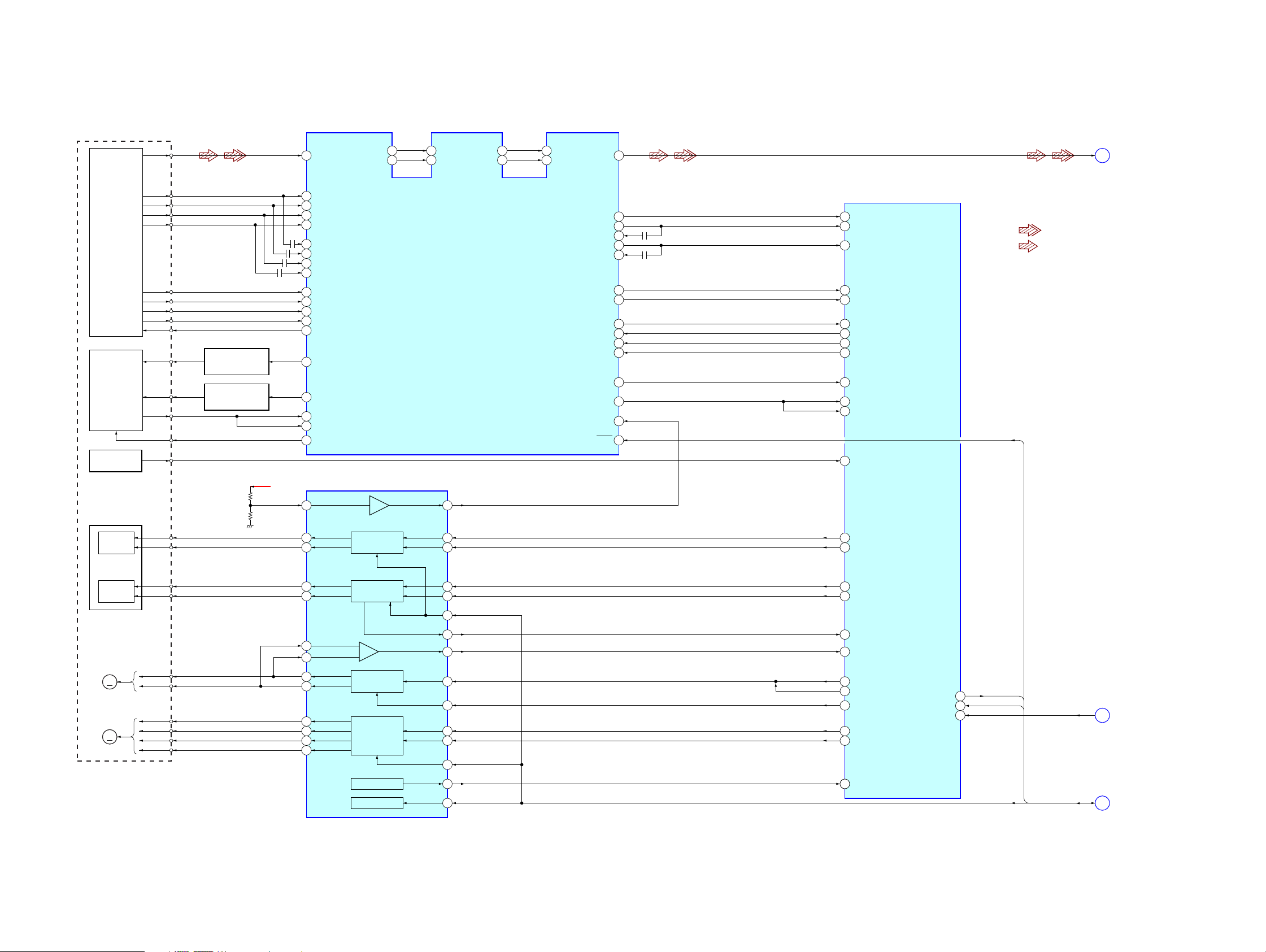
6-1. BLOCK DIAGRAM – RF/SERVO Section – • Refer to servicing notes (page 4) for discrimination of TYPE A/B.
OPTICAL PICK-UP
BLOCK
(KHM-240AAA) (TYPE A)
(KHM-270AAA) (TYPE B)
ATOP
RF
2
RF IN
ATON
64
63
AIP
61
AIN
62
FNP
FNN
55
54
DIP
56
DIN
57
SIGO
59
RF+
DVP-S90D
A
(Page 24)
DVD/CD
DETECTOR
DVD/CD
LASER
DIODE
MODULE
INLIMIT
SENSOR
2-AXIS
DEVICE
FOCUS
COIL
DVD LD
CD LD
SW
INLIM
FCS+
FCS–
A
B
C
D
E
F
G
H
VC
AUTOMATIC POWER
CONTROL (FOR DVD)
Q001
AUTOMATIC POWER
CONTROL (FOR CD)
PD
Q002
D+3.3V
14
A
13
B
12
C
11
D
7
A2
8
B2
9
C2
D2
10
E
15
F
16
G
17
H
18
VC
19
DVDLD
25
CDLD
26
DVDPD
21
CDPD
22
LDSELO
24
FOCUS/TRACKING COIL DRIVE,
SPINDLE/SLED MOTOR DRIVE
42
37
36
IC401
FOCUS COIL
DRIVE
DVD/CD RF AMP,
FOCUS/TRACKING ERROR AMP
IC001
40
48
1
TZIN
MIRR
TZC
SRD
SWD
SCLK
SDEN
DFT
MON
VCI
LDON
FE
42
TE
41
40
PI
36
PII
35
33
37
45
46
47
48
38
44
39
27
136
135
137
197
196
173
174
175
180
185
184
172
166
204
205
ADC1
ADC0
ADC2
MIRR
TZC
GIO6/SDI
GIO7/SDO
GIO8/SCK
GIO13
DFCTI
ADC7
GIO5/PGIN
GIO0/INT2
PDM2
PDM3
SERVO DIGITAL
SIGNAL PROCESSOR
IC302 (1/2)
• SIGNAL PATH
: DVD PLAY
: CD PLAY
XLDON
TRACKING
COIL
MM
(SPINDLE)
MM
(SLED)
TRK+
TRK–
SPM+
SPM–
SLA+
SLA–
SLB+
SLB–
35
34
46
47
27
28
32
31
30
29
TRACKING COIL
DRIVE
–
+
SPINDLE MOTOR
DRIVE
SLED MOTOR
DRIVE
TSD-M
POWER SAVE
3
4
19
5
45
13
21
7
10
20
22
39
202
203
139
140
159
161
167
198
199
7
168
PDM0
PDM1
ADC3
ADC4
MDSO
MDPO
GIO1/INT3
PWM0
PWM1
GIO2/INT4
HINT
HCS
XDSPRST
22
24
156
XSDPIT
XSDPCS
XDRVMUTE
XRST
XLDON
XSDPIT, XSDPCS,
XDRVMUTE
C
(Page 24)
B
(Page 25)
2323
Page 24
DVP-S90D
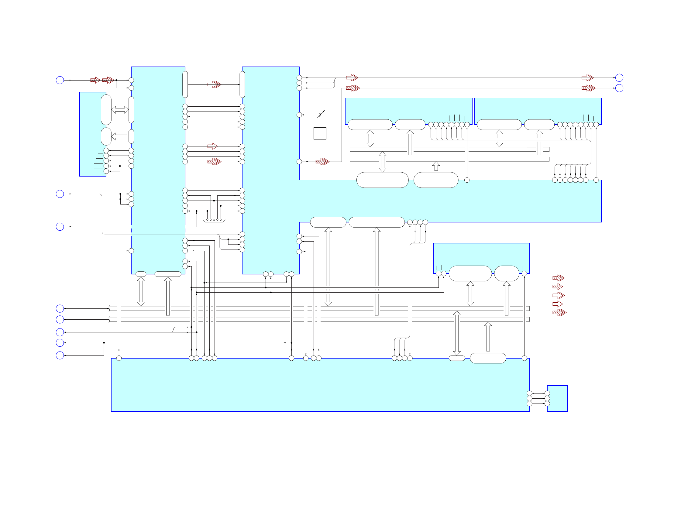
6-2. BLOCK DIAGRAM – MAIN Section (1/2) –
ARP
IC302 (2/2)
(Page 25)
(Page 25)
(Page 25)
(Page 25)
(Page 23)
RF+
A
(Page 23)
MEMD0 –
MEMD15
2 – 5, 7 – 10,
41 – 44, 46 – 49
MEMA0 –
A0 – A9 I/O0 – I/O15
21 – 24,
17
WE
OE
33
18
34
35
33MARP
MEMA9
27 – 32
36 71 67 62 17
D-RAM
IC303
RAS
UCAS
LCAS
33MARP, 33MAVD,
27MAVD, 512FSAVD
D
(Page 25)
TRST
E
(Page 25)
HD8 – HD11
F
HA0 – HA3, HA19
G
XRD, XWRH XWRH
H
XRST
I
XRST
C
131
128
38
42
41
39
182
187
189
157
XARPRST
RFIN1
RFIN2
44 – 51, 53 – 60
27 – 36
MA0 – MA9 MD0 –MD15
XMWR
XOE
XRAS
XCAS
CLKIN
MCKI
SCKI
XARPRST
HD8 – HD15
11 – 15, 17 – 192 – 9
A0 – A7D0 – D7
HA0 – HA7
SOI0 –SOI7
SD0 – SD7
73 – 76, 78 – 81
SDCK
68 41
XSHD
69 44
XSRQ
70 46
XSAK
71 45
SDEF
72 43
DATA
62 23
BCLK
63 25
LRCK
65 26
DOUT
66 22
TDO
195 118
TDI
193 119
TCK
194 120
TMS
192 121
TRST
191 122
(FOR JTAG)
XINT
21
XCS
23
XWAT
25
XWRH
207
XRD
208
XRD
70
XRD
XWRH
XWAIT
CS4X
INT1
33MAVD
27MAVD
512FSAVD
DTI0 – DTI7
31 – 34, 36 – 39
ICLKI
ISTARTI
IREQO
IVALI
IERRI
CDIN1I
CDBCKI
CDLRKI
CDIN2I
TDI
TDO
TCK
TMS
TRST
CRPCLKI
29
CLKI
180
SCLKI
182
ACLK
12
DATA BUS
ADDRESS BUS
COMPOUT
YOUT
COUT
VREFI
HAD23
HAD22
HIREQ0
HCSB
HRWB
220 221 224 231
HWAITOB
80
74
7
84
RV501
VIDEO
LEVEL
DO
20
AV DECODER
IC503
223 – 235, 237 – 240,
190
191
223
RSTB
35 16 61 60
INT0
XRST
CS3X
SYSTEM CONTROLLER
IC103 (1/2)
V
Y
C
DQ0 – DQ15
2, 3, 5, 6, 8, 9, 11, 12, 39,
40, 42, 43, 45, 46, 48 ,49
177, 174, 171, 168, 165, 163,
160, 158, 157, 159, 162, 164,
167, 170, 173, 176
SDDQ0 – SDDQ15
HD0 – HD15 HAD0 – HAD21
2 – 5, 7 – 10
HD0 – HD15
CS2X
218 – 215, 213 – 210, 208 – 205,
203 – 200, 198 – 195, 193, 192
HA0 – HA21
16MB SDRAM
IC504
A0 – A11
21 – 24, 27 – 32,
20, 19
226 227 228 229
DACK0
DACK1
DREQ0
49504647
DACK1
DACK0
DREQ0
35 34 14 36 15 16 17 18
CLK
SDRAM DATA BUS
SDRAM ADDRESS BUS
134, 131, 128, 125, 124,
127, 130, 133, 136, 139,
137, 140
SDAD0 – SDAD11
DM ACK1
DM REQ1
DM ACK0
DM REQ0
DACK0
DREQ0
DACK1
DREQ1
DATA BUS
ADDRESS BUS
DREQ1
DREQ1
CLK
CKE
DQML
DQMUWECAS
RAS
CS
CKE
DQML
DQMUWECAS
RAS
144
SDCS0B
FLASH MEMORY
DQ0 – DQ15
WECEOE
31, 33, 35, 38, 40, 42,
11 26
28
44, 30, 32, 34, 36, 39, 41,
43, 45
HD0 – HD15
HD0 – HD15
85 – 100
HD0 – HD15
DQ0 – DQ15 A0 – A11
2, 3, 5, 6, 8, 9, 11, 12, 39,
40, 42, 43, 45, 46, 48 ,49
IC107
A0 – A20
25, 24 – 18,
8 – 1, 48, 17,
16, 9, 10
HA0 – HA21
102 – 109, 111 – 118,
120, 1 – 5
HA0 – HA21
HA1 – HA21
16MB SDRAM
21 – 24, 27 – 32,
58
CS0X
SDA
38
SCL
39
WP
7
IC505
20, 19
CLK
CKE
35 34 14 36 15 16 17 18
CLK
CKE
DQML
CLK
CKE
DQML
DQMU
149 146 155 154 152 151 147
SDCLKO
SDCKEO
SDDQM0
• SIGNAL PATH
: DVD PLAY
: CD PLAY
: DVD/CD PLAY (VIDEO)
: DVD/CD PLAY (AUDIO)
: DVD/CD PLAY (DIGITAL OUT)
EEPROM
IC101
5
SDA
6
SCL
7
WP
DQML
DQMUWECAS
DQMUWECAS
WE
CAS
SDDQM1
SDWEOB
RAS
RAS
SDCKCOB
SDRASOB
RAS
143
V, Y, C
SPDIF
CS
SDCS1B
J
K
(Page 25)
(Page 25)
2424
Page 25

6-3. BLOCK DIAGRAM – MAIN Section (2/2) –
V, Y, C
J
(Page 24)
SPDIF
K
(Page 24)
WIDE
82
SYSTEM CONTROLLER
IC103 (2/2)
X1
53
X0
54
XLDON
84
INT2
18
CS5X
63
XDRVMUTE
48
48/44.1k
SO0
SC0
XIFCS
INT4
MAMUTE
XFRST
SO2
CPUCK
CS6X
INT3
SI0
SI2
26
25
27
51
20
83
76
32
31
77
65
19
TRST
E
(Page 24)
XLDON, XSDPIT, XSDPCS
XDRVMUTE
B
(Page 23)
HD8 – HD11
F
(Page 24)
HA0 – HA3, HA19
G
(Page 24)
XRD, XWRH
H
(Page 24)
XRST
I
(Page 24)
X101
16.5MHz
XLDON
XSDPIT
XSDPCS
XDRVMUTE
XIFINT
XIFOK
XFRRST
X102
27MHz
CN103
12TXD
RXD
DATA BUS
ADDRESS BUS
(FOR TEST)
HD8 – HD11
HA0 – HA3,
XRD
XWRH
CLOCK GENERATOR
IC102
XTO
XTI
FSEL
IC106 (1/3)
1
2
4
5
12
13
33-1OUT
33-2OUT
27-1OUT
512-1OUT
3
6
IC106 (2/3)
11
IC106 (3/3)
8
CK
48
CS5
12
INT
18 – 15
D0 – D3
5 – 1
SHA0 – SHA3.
11
RDN
10
WRN
9
XRST
GATE ARRAY
SHA19
8 15
7
1481
HA19
13
10
3
IC202
D+5V
B+
IFSO0
IFSI0
IFSC0
XIFCS
512FSAVD
TRMP
TRMM
CKMM
CKMP
DSW1
V
Y
C
VIDEO SWITCH
Q711, 712
33MARP
33MAVD
27MAVD
33
32
36 – 34
TSW1 – TSW3
28
29
27
7
4
2
LOADING MOTOR
DRIVE
IC701
SUB TRAY1 – 3
HEIGHT SENSOR
IC731 – 733
Q701
VIDEO BUFFER
IC701
MUTE
1
OUTC1
OUTC2
OUTB1
OUTB2
OUTA1
OUTA2
10
9
13
12
15
14
INC
INB
INA
MM
S741
ON: WHEN SUB TRAY SLIDES OUT
(IN)
OF THE CHUCKING POSITION
S742
ON: WHEN SUB TRAY IS
(OUT)
CHUCKING POSITION
DISC IN
DETECT
IC751
M721
(LOADING)
2
3
4
1
OPTICAL
TRANSMITTER
IC201
33MARP, 33MAVD,
27MAVD, 512FSAVD
IFSO0, IFSI0, IFSC0, XIFCS,
XIFINT, XIFOK, XFRRST
• SIGNAL PATH
: DVD/CD PLAY (VIDEO)
: DVD/CD PLAY (DIGITAL OUT)
VIDEO OUT
S VIDEO OUT
OPTICAL
TO ST-S90D
VMUTE
DVP-S90D
J202
J201
OUT
L
(Page 26)
D
(Page 24)
M
(Page 26)
2525
Page 26

DVP-S90D
6-4. BLOCK DIAGRAM – INTERFACE CONTROL Section –
IFSO0, IFSI0, IFSC0,
XVIFCS, XIFINT, XIFOK,
XFRRST
M
(Page 25)
VMUTE
L
(Page 25)
S701 – 708
IFSO0
IFSI0
IFSC0
XVIFCS
XIFINT
XIFOK
XFRRST
36
SYS DATAIN
35
SYS DATAOUT
37
SYS CLK
19
SYS CS
42
SYS RQ
43
SYS OK
40
SYS RST
INTERFACE CONTROLLER
97
KEY0
EXP-OUT DATA
EXP-IN DATA
REC/PB/PAS
IC401
EXP-CLK
EXP-LAT
KEY2
A-TRIG
B-TRIG
A-SHUT
B-SHUT
B-HALF
IIC DATA
IIC CLK
RESET
VMUTE
85
84
87
86
94
55
53
59
89
90
91
30
29
12
48
D+5V (LED)
B+
INTERFACE CONTROLLER (IC401) B+
GATE ARRAY (IC202), MOTOR/COIL DRIVE (IC401),
SERVO DSP (IC503), VIDEO BUFFER (IC701) B+
EVER+5V
D+5V
RF SECTION,
SERVO DSP (IC302) B+
+3.3V
D514
D513
D512
+5V REGULATOR
IC502
+3.3V REGULATOR
IC301
RECT
D501 – 504
CN103
10
DATA-OUT
DATA-IN
9
CLK
8
LAT
7
KEY2
6
ATRIG
4
BTRIG
5
REC/PB/PAS
11
ASHUT
12
BSHUT
13
BHALF
14
UNREG
3
CN102
UNREG (TC)
7
CN101
I2C-DATA
2
I2C-CLK
1
MRESET
4
V-MUTE
3
AC
8
AC
9
EVER+5V
5
POWER BLOCK
+5V
SYSTEM CONTROL 5
FROM TC-S90D
SYSTEM CONTROL 3
FROM ST-S90D
S711 – 720
D701 – 705
X401
16MHz
95
KEY0
LED DISC1
LED DISC3
LED PLAY
65 – 83, 88
LED PAUSE
13
X-OUT
15
X-IN
+3.3V
AV DECODER (IC503) B+
EEPROM (IC101), CLOCK GENERATOR (IC102),
GATE ARRAY (IC202), D-RAM (IC303),
ı
P-CONT
44
D+3.3V
SYSTEM CONTROLLER (IC103),
FLASH MEMORY (IC107),
SDRAM (IC504, 505) B+
+1.8V
SERVO DSP (IC302),
AV DECODER (IC503) B+
+1.8V
AV DECODER (IC503) B+
M+12V
MOTOR/COIL DRIVE (IC401) B+
M+7V
MOTOR DRIVE (IC701) B+
+3.3V REGULATOR
IC502
+1.8V REGULATOR
IC006
+1.8V REGULATOR
IC501
+7V REGULATOR
IC501
+3.3V
M+12V
+12V
P. CONT
AC IN
TO TA-S90D
2626
Page 27

DVP-S90D
d
d
6-5. NOTE FOR PRINTED WIRING BOARDS AND SCHEMATIC DIAGRAMS
Note on Printed Wiring Board:
• X : parts extracted from the component side.
• Y : parts extracted from the conductor side.
f
•
• : Pattern from the side which enables seeing.
Caution:
Pattern face side: Parts on the pattern face side seen from
(Conductor Side) the pattern face are indicated.
Parts face side: Parts on the parts face side seen from
(Component Side) the parts face are indicated.
• MB board is multi-layer board.
: internal component.
However, the patterns of intermediate-layer not been included
in diagram.
Note on Schematic Diagram:
• All capacitors are in µF unless otherwise noted. pF: µµF
50 WV or less are not indicated except for electrolytics
and tantalums.
• All resistors are in Ω and 1/
specified.
f
•
• C : panel designation.
Note: The components identified by mark 0 or dotted line
• A : B+ Line.
• H : adjustment for repair.
•Voltages and waveforms are dc with respect to ground
•Voltages are taken with a VOM (Input impedance 10 MΩ).
•Waveforms are taken with a oscilloscope.
• Circled numbers refer to waveforms.
• Signal path.
• Abbreviation
• Refer to servicing notes (page 4) for discrimination of
: internal component.
with mark 0 are critical for safety.
Replace only with part number specified.
under no-signal conditions.
no mark : DVD PLAY
(): CD PLAY
Voltage variations may be noted due to normal production tolerances.
Voltage variations may be noted due to normal production tolerances.
c : DVD PLAY
J : CD PLAY
L : DVD/CD PLAY (VIDEO OUT)
F : DVD/CD PLAY (AUDIO OUT)
I : DVD/CD PLAY (DIGITAL OUT)
AUS : Australian model
EA : Saudi Arabia model
SP : Singapore model
E15 : 220 – 240 V AC Area in E model
TYPE A/B.
4
W or less unless otherwise
• Circuit Boards Location
SUB PANEL board
MB board
PANEL board
VIDEO board
MAIN boar
IN OUT SW board
TRAY SENSOR board
RF board
DRIVER boar
MOTOR board
DISC SENSOR board
2727
Page 28
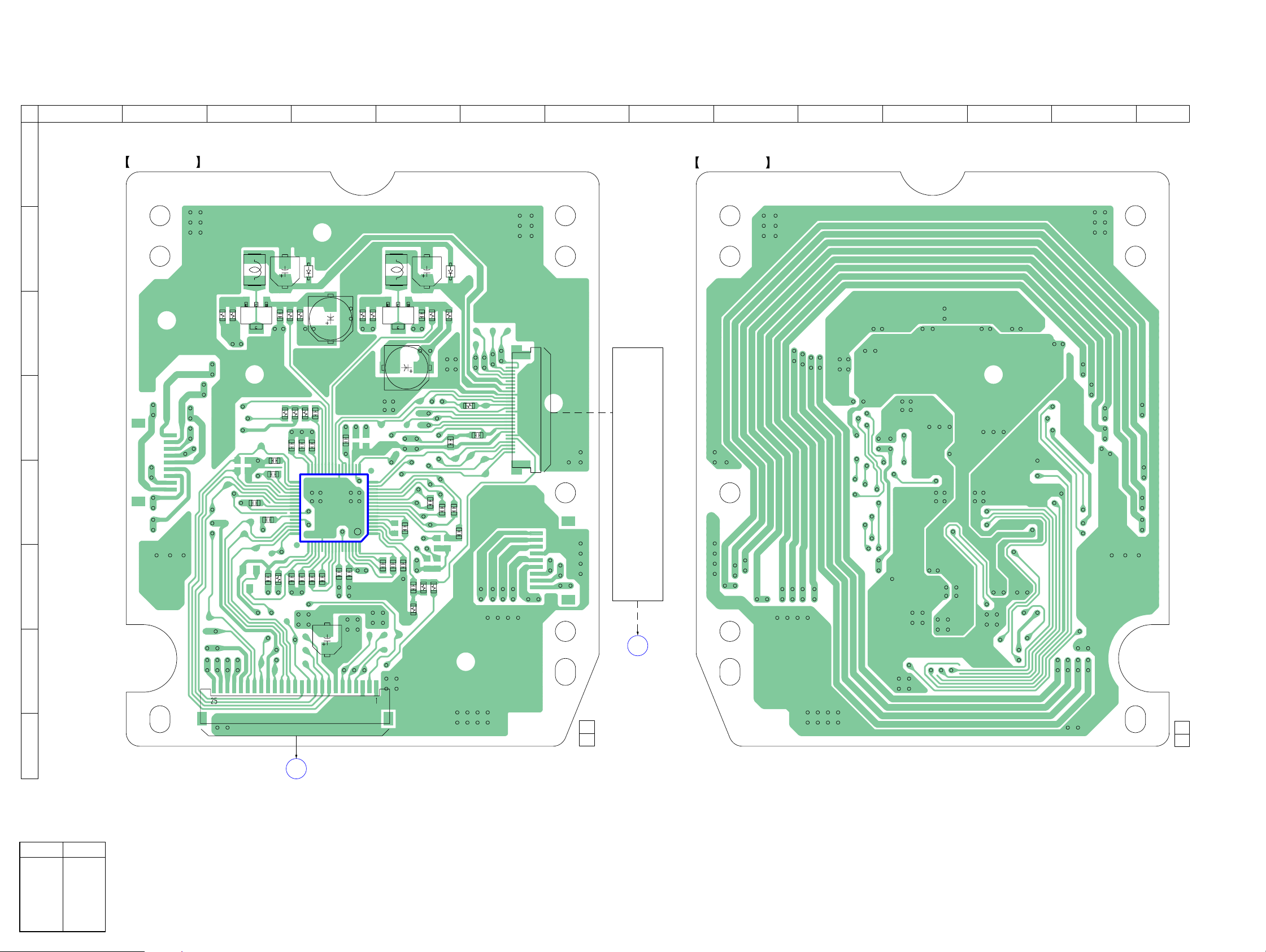
DVP-S90D
6-6. PRINTED WIRING BOARD – RF Board – • See page 27 for Circuit Boards Location. • Refer to servicing notes (page 4) for discrimination of TYPE A/B.
1 2 3 4 5 6 7 8 9 10 11 12 13 14
A
RF BOARD
B
C
D
E
F
(COMPONENT SIDE)
R023
L002
R020
E
Q002
C047
C
B
R006
C048
C043
C039
C021
C024
R029
R005
C040
C046
33
48
C035
R037
R025
R038
C038
C033
D004
C034
C036
IC001
C032
C031
C023
C026
C028
R008
1732
6449
C027
R007
16
1
C022
L001
E
Q001
C025
C
C017
C016
C015
B
C019
C009
C018
R045
R011
C008
C007
R002
C002
D001
R010
C006
R003
C005
C001
26
CN001
1
OPTICAL
PICK-UP
BLOCK
(KHM-240AAA)
(TYPE A)
(KHM-270AAA)
(TYPE B)
RF BOARD
(CONDUCTOR SIDE)
G
H
• Semiconductor
Location
Ref. No. Location
D001 B-5
D004 B-4
IC001 E-4
Q001 C-5
Q002 C-3
CN002
A
C044
MB BOARD
CN010
(Page 32)
R009
1-682-815-
(11)
B
MB BOARD
CN015
(Page 32)
11
1-682-815-
2828
11
(11)
Page 29

6-7. SCHEMATIC DIAGRAM – RF Board – • See page 47 for PIN FUNCTION. • Refer to servicing notes (page 4) for discrimination of TYPE A/B.
OPTICAL
PICK-UP
BLOCK
(KHM-240AAA)
(TYPE A)
(KHM-270AAA)
(TYPE B)
DVP-S90D
(Pageg 34)
(Pageg 34)
IC001
2929
Page 30

DVP-S90D
6-8. PRINTED WIRING BOARDS – DISC SENSOR/DRIVER/IN OUT SW/MOTOR/TRAY SENSOR Boards – • See page 27 for Circuit Boards Location.
1 2 3 4 5 6 7 8
A
B
C
1
5
C
B
D
E
C
MB
BOARD
CN203
(Page 32)
• Semiconductor
Location
Ref. No. Location
IC701 D-8
IC731 A-1
IC732 A-2
IC733 A-4
IC751 E-5
3030
Q701 B-8
Page 31

6-9. SCHEMATIC DIAGRAM – DISC SENSOR/DRIVER/IN OUT SW/MOTOR/TRAY SENSOR Boards –
RPI-321
IC731
SUB TRAY1
HEIGHT SENSOR
DVP-S90D
IC732
SUB TRAY2
HEIGHT SENSOR
IC733
SUB TRAY3
HEIGHT SENSOR
IC701
RPI-321
RPI-321
C
MB
BOARD (6/6)
CN203
(Page 39)
IC751
DISC IN
DETECT
3131
Page 32

DVP-S90D
6-10. PRINTED WIRING BOARD – MB Board (Component Side) – • See page 27 for Circuit Boards Location.
• Semiconductor
Location
Ref. No. Location
IC006 H-5
IC103 H-10
IC202 F-10
IC302 E-5
IC503 H-7
1 2 3 4 5 6 7 8 9 10 11
A
MB BOARD
B
C
A
RF BOARD
CN002
D
(Page 28)
CN010
E
F
(COMPONENT SIDE)
L701
C315
R313
C309
C312
R316
C304
R345
R336
C320
R314
C319
R337
R338
R343
C310
R315
R341
C317
R334
C313
R317
C311
R319
R342
C324
R356
C351
C352
105
C306
C307
C347
C348
R385
C349
156
104
R349
R352
157
R328
C331
R368
R332
IC302
C766
C345
R330
C336
R384
60 1
61
53
208
52
C339
C340
R107
1
R140
R137
R509
C765
C106
C105
R125
R510
R740
C701
C764
C104
C107C108
X102
C111
R739
R508
F
CN012
240
VIDEO BOARD
CN201
(Page 42)
C745
C743
FB714
R719
C744
C742
36 25
37
IC202
48
1
R203
R206
R207
CN203
24
13
C
DRIVER
BOARD
CN701
(Page 30)
C505
R412
C420
C404
R413
R414
R415
R425
C422
C406
R301
R439
R302
C004
C401
R417
C405
R304
R327
G
R419
C403
C414
H
R433
R432
C416
C418
C419
I
CN015
J
OPTICAL
PICK-UP
B
BLOCK
(Page 28)
C512
C521
IC006
R518
13
C005
R522
C006
120
121
15
RV501
CN404
(FOR TEST)
C529
D
IC503
MAIN BOARD
NO106
(Page 40)
CN008
R525
180
181
C506
C502
10
R174
9
120 91
1
30
31 60
R121
R182
R106
R114
R185
R186
R164
R165
CN101
MAIN BOARD
E
CN107
(Page 40)
IC103
R111
R133
R105
X101
C110
R170
C501
CN103
(FOR TEST)
15
90
R129
R179
R143
61
C112
1-682-900-
11
(11)
3232
Page 33

6-11. PRINTED WIRING BOARD – MB Board (Conductor Side) – • See page 27 for Circuit Boards Location. • Refer to servicing notes (page 4) for discrimination of TYPE A/B.
DVP-S90D
1 2 3 4 5 6 7 8 9 10
• Semiconductor
Location
Ref. No. Location
IC101 I-3
A
MB BOARD
(CONDUCTOR SIDE)
IC102 E-5
IC106 I-3
IC107 G-3
IC301 F-9
IC303 D-7
IC401 H-9
IC501 I-4
B
IC502 G-8
IC504 H-6
IC505 G-6
R737
R738
C721
R713
IC701
FB712
R718
FB711
C741
C
R717
Q712
9
16
B
C702
E
R142
R126
R138
C
R725
R724
C
Q711
EB
D
R211
C205
R212
FL202
C204
C202
C206
C203
R202
FL204
R215
FL203
R210
R214
R209
R208
E
C207
R141
R712
8
R711
1
F
C504
R517
C547
C546
R021
C516
FL505
C514
R532
C508
C532
C526
R017
C509
C530
C545
R112
R156
25
G
H
I
R184
R183
R145
R113
FL103
48
C124
R163
C103
FL102
J
IC107
R155
R153
R151
C109
C114
R119
R147
R168
85
14
IC101
C116
R154
R116
R152
R117
R118
R150
C113
R128
R130
8
14
IC106
R187
R167
R175
R166
R172
R123
R146
FL502
21
3
IC501
R507
R134
C523
C524
C525
R554
24
R162
R160
R161
C119
1
R149
R132
R157
R131
7
1
R188
C716
C711
FL101
IC102
9
16
C535
C722
L715
C717
L713
C712
L711
R101
FB112
IC505
IC504
C531
C534
C007
8
1
C533
R109
R124
C510
C342
R533
FB011
R320
C343
C341
R136
C344
C511
FL005
C536
1
11
15
25
C538
C539
FB012
C337
IC303
C338
C513
C520
C537
C542
R524
C522
R515
C540
C519
C518
C541
R516
FL501
50
40
36
26
C335
R513
C503
FB007
C334
C350
R512
R511
R514
13
54
IC502
C018
FL004
FB010
FB009
FB008
FL003
R521
C019
R321
C333
C325
C326
R318
R312
C332
C318
R335
C327
C346
R428
C415
R435
R310
R311
C321
R416
C411
13
18
50
19
24
R701
R306
R308
R199
R411
R424
C429
R307
R299
C305
R423
R305
R351
R350
R409
R309
R344
C323
C328
R420
C322
R410
C430
R426
12
IC401
25 5130 31
R080
IC301
453
4976
R329
R408
R422
C408
C301
1
R407
R421
C407
1
36
C402
(TYPE A)
R406
R418
R427
48
C413
43
52
42
37
R434
C417
R430
R429
C412
R431
R078
R076
R077
1-682-900-
11
(11)
IC701 C-5
Q711 D-4
Q712 D-4
3333
Page 34

DVP-S90D
6-12. SCHEMATIC DIAGRAM – MB Board (1/6) – • Refer to servicing notes (page 4) for discrimination of TYPE A/B.
(Page 35)
(Page 29)
(Page 35)
(Page 39)
(Page 38)
(Page 37)
(Page 35)
IC401
(TYPE A)
∗
R077
330 (TYPE A)
10k (TYPE B)
(Page 37)
∗
(Page 35)
(Page 29)
(Page 35)
(Page 36)
(Page 37)
IC006
(Page 41)
(Page 39)
3434
Page 35
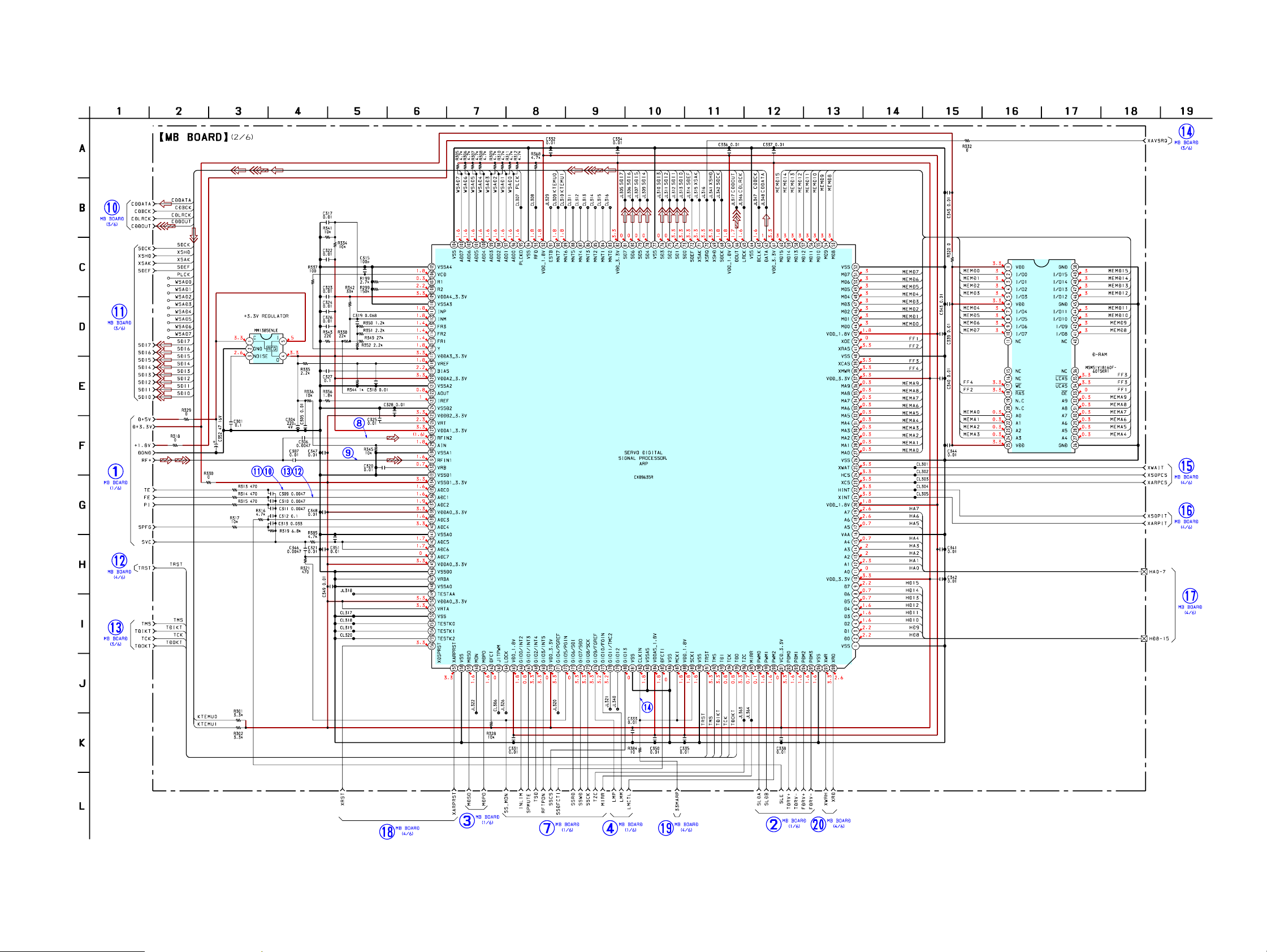
6-13. SCHEMATIC DIAGRAM – MB Board (2/6) – • See page 51 for PIN FUNCTION.
(Page 36)
DVP-S90D
(Page 36)
(Page 36)
(Page 34)
(Page 37)
(Page 36)
IC301
IC303
IC302
(Page 37)
(Page 37)
(Page 37)
(Page 37)
(Page 34)
(Page 34) (Page 34) (Page 37)
3535
(Page 34)
(Page 37)
Page 36

DVP-S90D
6-14. SCHEMATIC DIAGRAM – MB Board (3/6) –
(Page 37)
(Page 37)
(Page 37)
(Page 37)
(Page 37)
(Page 37)
(Page 35)
(Page 38)
IC503
IC504
IC505
(Page 37)
(Page 37)
(Page 35)
(Page 35)
(Page 34)
(Page 38)
IC501
IC502
(Page 37)
(Page 35)
3636
Page 37

6-15. SCHEMATIC DIAGRAM – MB Board (4/6) – • See page 49 for PIN FUNCTION.
DVP-S90D
(Page 36)
(Page 35)
(Page 39)
(Page 35)
(Page 36)
(Page 34)
(Page 36)
(Page 39)
(Page 35)
(Page 36)
IC101
(Page 36)
(Page 39)
IC107
IC103
(Page 35)
(Page 36)
(Page 38)
(Page 34)
(Page 35)
(Page 35)
(Page 36)
(Page 36)
(Page 39)
IC102
(Page 41)
(Page 38)
(Page 35)
IC106
(Page 36)
(Page 34)
3737
Page 38
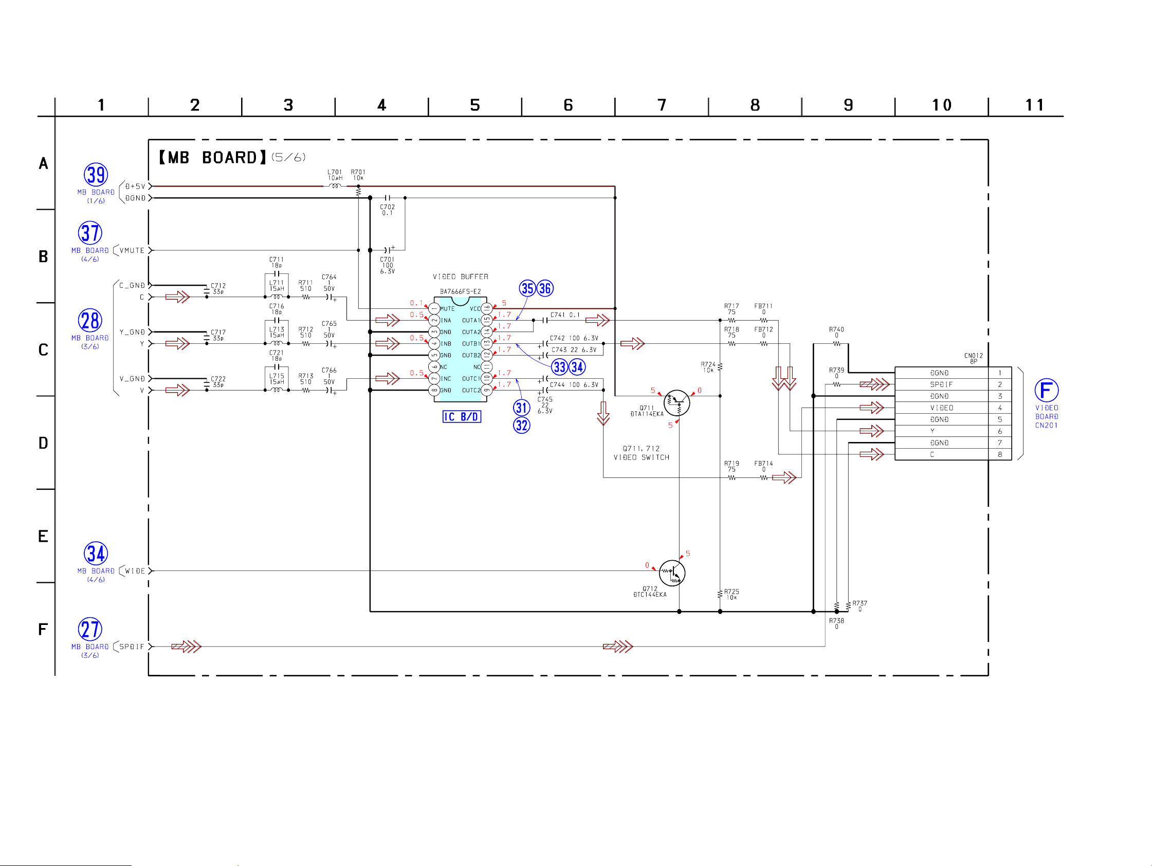
DVP-S90D
6-16. SCHEMATIC DIAGRAM – MB Board (5/6) –
(Page 34)
(Page 37)
IC701
(Page 36)
(Page 37)
(Page 43)
(Page 36)
3838
Page 39
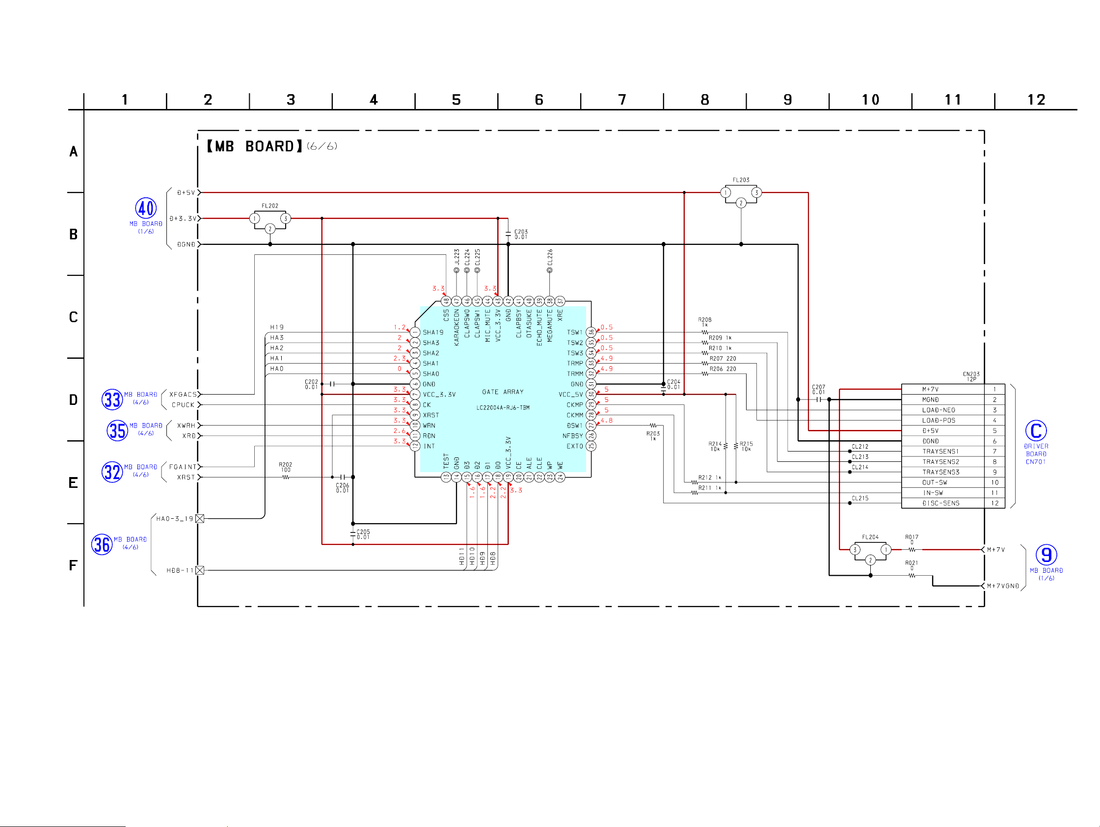
6-17. SCHEMATIC DIAGRAM – MB Board (6/6) –
(Page 34)
DVP-S90D
(Page 37)
(Page 37)
(Page 37)
IC202
(Page 37)
(Page 31)
(Page 34)
3939
Page 40

DVP-S90D
6-18. PRINTED WIRING BOARD – MAIN Board – • See page 27 for Circuit Boards Location.
1 2 3 4 5 6 7 8 9 10
C557
D513
D512
R103
R102
R101
MB BOARD
CN008
(Page 42)
C506
1
FB503
C513
D505
C514
1
C509
CN101
9
1
JW102
NO104
IC501
IC502
C500
POWER BLOCK
JW103
C101
C102
C512
C508
JW105
9
JW107
D504
EL103
LP101
LP102
C501
D503
EL101
JW101
EL102
D502
AC IN
TO TA-S90D
1
8
JW151
CN102
D501
JW100
1
15
2
CN103
14
1-682-811-
SYSTEM CONTROL 5
11
(11)
CN103
FROM TC-S90D
MB BOARD
E DG
CN101
R411
C406
CN107
JW130
C411
R496
R483
(Page 32)
JW127
C401
JW125
JW121
9
10
JW124
JW123
EL104
C427
R427
R493
R488
R412
JW120
C425
R482
R134
R494
R491
R485
JW119
JW118
JW117
R425
R490
R484
R133
R489
MAIN BOARD
A
4
1
CN501
(FOR TEST)
B
CN401
9
JW145
R465
R469
R473
R477
1
R481
R434
C407
1
CN503
(FOR TEST)
R431
R433
JW143
JW144
R435
R441
C
10
R443
EL105
JW140
LP104
R447
R457
R444
R456
JW138
R448
R453
R455
JW137
JW133
R454
R442
R451
R459
R437
R436
C402
JW132
51
R440
50
C408
R432
R419
JW131
R430
31 30
IC401
R567
R429
80
R497
1
2
LP103
JW128
R417
R413
JW146
R409
C403
JW126
JW147
C404
X401
1
100
81
R480
R492
R495
R487
JW115
JW113
JW114
R132
R486
VIDEO BOARD
CN202
(Page 42)
FB502
NO105
1
C505
C502
JW111
C405
2
JW402
R104
JW407
8
JW108
FB501
NO106
C504
C507
D514
D105
D
H
• Semiconductor
Location
Ref. No. Location
D105 D-7
D501 C-9
D502 C-9
D503 C-9
D504 C-9
D505 C-8
D512 D-8
D513 C-8
D514 C-8
IC401 C-4
IC501 B-8
IC502 C-8
PANEL BOARD
NO703
(Page 42)
SYSTEM CONTROL 3
FROM ST-S90D
4040
Page 41
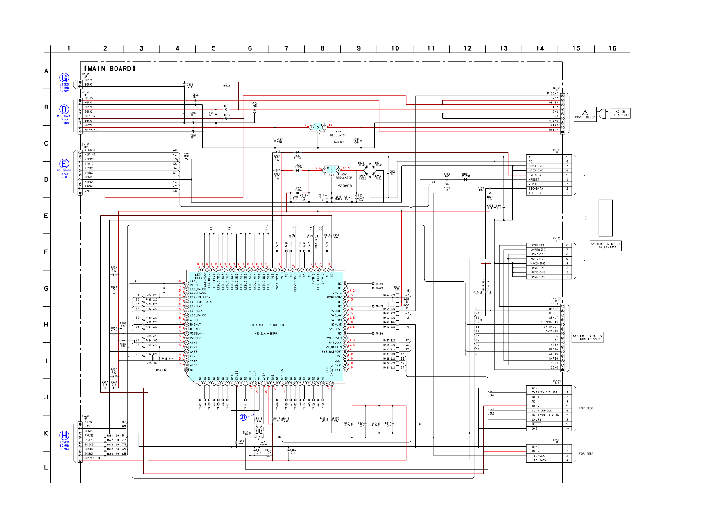
6-19. SCHEMATIC DIAGRAM – MAIN Board – • See page 55 for PIN FUNCTION.
(Page 43)
(Page 34)
DVP-S90D
IC501
(Page 37)
IC502
IC401
(Page 43)
4141
Page 42

DVP-S90D
6-20. PRINTED WIRING BOARDS – PANEL/SUB PANEL/VIDEO Boards – • See page 27 for Circuit Boards Location.
1 2 3 4 5 6 7 8 9 10
J202
A
VIDEO BOARD
VIDEO OUT
PANEL BOARD
J201
NO703
19
H
R712
R711
B
C
S715
x
D
S718
RETURN NEXT PREV
R714
R713
S712
M
R715
S713
>
D701
S716
D701, S716
X
S720
R716
R718
S711
m
S714
.
D702
S717
S719
BOARD
CN401
(Page 40)
D702, S717
N
R717
MAIN
S VIDEO OUT
FB201
D704
FB204
C206
JW201
(DISC 2)
31
IC201
CN201
MB BOARD
F G
CN012
(Page 32)
(DISC 1)
12
34
FB202
D703
3 2 1
(DISC 3)
FB203
D705
IC201
OPTICAL
OUT
TO ST-S90D
C203
C204
CN202
L201
12
MAIN BOARD
NO105
(Page 40)
NO702
1-682-813-
1
2
(11)
SUB PANEL BOARD
11
S701 – 708S711 – 720
S706
Z
(DISC 3)
NO701
S701
1
DISC 3 DISC 2 DISC 1
2
R701
S707
R706
R705
S705
Z
(DISC 2)
S702
R702
S708
PLAY MODEREPEAT
R707
R704
S704
Z
(DISC 1)
S703
R703
• Semiconductor
Location
Ref. No. Location
D701 C-2
D702 C-2
D703 C-5
D704 C-6
D705 C-7
IC201 A-7
R719
1-680-995-
(11)
11
1-680-996-
11
(11)
4242
Page 43

6-21. SCHEMATIC DIAGRAM – PANEL/SUB PANEL/VIDEO Boards –
DVP-S90D
IC201
(Page 38)
(Page 41)
(Page 41)
4343
Page 44

DVP-S90D
•Waveforms
– RF Board –
– MB Board –
1 IC001 2 (RF IN) (DVD PLAY)
2 IC001 2 (RF IN) (CD PLAY)
3 IC001 ra (TE) (DVD PLAY)
Approx.
570 mVp-p
Approx.
550 mVp-p
6 IC001 rs (FE) (CD PLAY)
Approx.
600 mVp-p
7 IC001 tl (SIGO) (DVD/CD PLAY)
Approx.
1.4 Vp-p
8 IC302 <zx, (RFIN2) (CD PLAY)
9 IC302 <zcz (RFIN1) (DVD PLAY)
0 IC302 <zcb (ADC0) (DVD PLAY)
Approx.
1.4 Vp-p
Approx.
1.4 Vp-p
qd IC302 <zcn (ADC1) (CD PLAY)
Approx.
600 mVp-p
qf IC302 <z,x (CLKIN), <z,m (MCKI), <z,. (SCKI)
3.4 Vp-p
29.5 ns
qg IC503 qs (ACLK) (DVD PLAY)
qk IC503 uf (YOUT) (COLOR BAR (NTSC))
1 Vp-p
H
ql IC503 uf (YOUT) (COLOR BAR (PAL))
1 Vp-p
H
w; IC503 uj (COUT) (COLOR BAR (NTSC))
wd IC503 i; (COMPOUT)
(COLOR BAR (PAL))
1 Vp-p
H
wf IC503 <z,/ (CLKI), <z,x (SCLKIN)
3.4 Vp-p
37 ns
wg IC103 tf (X0)
4 IC001 ra (TE) (CD PLAY)
5 IC001 rs (FE) (DVD PLAY)
Approx.
120 mVp-p
Approx.
800 mVp-p
Approx.
180 mVp-p
qa IC302 <zcb (ADC0) (CD PLAY)
qs IC302 <zcn (ADC1) (DVD PLAY)
Approx.
120 mVp-p
Approx.
800 mVp-p
Approx.
180 mVp-p
40.7 ns
qh IC503 qs (ACLK) (CD PLAY)
44.3 ns
qj IC503 wl (CRPCLKI)
3.4 Vp-p
3.4 Vp-p
3.4 Vp-p
710 mVp-p
H
wa IC503 uj (COUT) (COLOR BAR (PAL))
710 mVp-p
H
ws IC503 i; (COMPOUT)
(COLOR BAR (NTSC))
1 Vp-p
1.8 Vp-p
60.6 ns
wh IC102 3 (27-1OUT)
3.4 Vp-p
37 ns
wj IC102 7 (XTI)
1.6 Vp-p
29.5 ns
H
37 ns
4444
Page 45
– MAIN Board –
DVP-S90D
wk IC102 9 (512-2OUT), 0 (512-1OUT)
(DVD PLAY)
3.4 Vp-p
40.7 ns
wl IC102 9 (512-2OUT), 0 (512-1OUT)
(CD PLAY)
3.4 Vp-p
44.3 ns
e; IC102 qd (33-2OUT), qg (33-1OUT)
ed IC701 qd (OUTB1) (COLOR BAR (NTSC))
2 Vp-p
H
ef IC701 qd (OUTB1) (COLOR BAR (PAL))
2 Vp-p
H
eg IC701 qg (OUTA1) (COLOR BAR (NTSC))
ej IC401 qd (X-OUT)
2.5 Vp-p
62.5 ns
3.4 Vp-p
29.5 ns
ea IC701 0 (OUTC1) (COLOR BAR (NTSC))
2 Vp-p
H
es IC701 0 (OUTC1) (COLOR BAR (PAL))
2 Vp-p
1.8 Vp-p
H
eh IC701 qg (OUTA1) (COLOR BAR (PAL))
1.8 Vp-p
H
H
45
Page 46

DVP-S90D
• IC Block Diagrams
– DRIVER Board –
IC701 BA6956AN
TSD
CONTROL LOGIC
1 2 3 4 5 6 7 8 9
OUT2
RNF
OUT1
VREF
– MB Board –
IC102 IMIC6001BTD
VM
VCC
FIN
GND
RIN
1
VDD
2
VSS
3
27-1OUT
27-2OUT
VDD
VSS
XTO
XTI
4
5
6
7
8
OSC PLL2
PLL1
IC701 BA7666FS-E2
MUTE
1 16
2
INA
GND
INB
GND
INC
GND
4
5
6
NC
7
6dB
6dB
6dB
75Ω
75Ω
75Ω
16
TEST
15
33-1OUT
FSEL
14
13
33-2OUT
12
VDD
VSS
11
512-1OUT
10
512-2OUT
9
VCC
15
OUTA1
143
OUTA2
13
OUTB1
12
OUTB2
11
NC
10
OUTC1
98
OUTC2
46
Page 47

6-22. IC PIN FUNCTION DESCRIPTION
• RF BOARD IC001 SP3728ACB (DVD/CD RF AMP, FOCUS/TRACKING ERROR AMP)
Pin No. Pin Name I/O Description
1, 2 RFIP, RFIN I
3CP—
4WINI
5 WPP O
6CN—
7 to 10 A2 to D2 I
11 to 14 D to A I
15 to 18 E to H I
19 VC O
20 VPB —
21 DVDPD I
22 CDPD I
23 VNB —
24 LDSELO O
25 DVDLD O
26
27
28
29
30
31
32
33
34
35
36
37
38
39
40
41
42
43
44
45
46
47
48
49
50
51
52
53
54, 55
56, 57
CDLD O
LDON I
MEVO O
MIN I
MP —
MB —
MLPF —
MIRR O
BYP2 —
PII I
PI O
TZC O
DFT O
VCI I
TZIN I
TE O
FE O
TPH —
MON O
SRD O
SWD I
SCLK I
SDEN I
V33 —
RX I
TPA —
MEV —
VNA —
FNN, FNP O
DIP, DIN I
RF signal input terminal
Tracking LPF terminal
Wobble detection signal input terminal Not used (open)
Wobble push-pull signal output terminal Not used (open)
Tracking LPF terminal
Photo detector interface input terminal (AC coupled input for the DPD and wobble)
Photo detector interface input terminal (main)
Photo detector interface input terminal (sub)
Reference voltage (+2.5V) output terminal
Power supply terminal (+5V) (servo block)
DVD APC signal input terminal
CD APC signal input terminal
Ground terminal (servo block)
APC LD select signal output terminal
DVD APC signal output terminal
CD APC signal output terminal
APC LD output control signal input terminal
Envelope signal output terminal for mirror
RF signal input terminal for mirror
Mirror top hold terminal
Mirror bottom hold terminal
Mirror LPF terminal
Mirror detect signal output to the servo DSP (IC302)
Servo AGC gain control terminal
Pull-in signal input terminal
Pull-in signal output terminal
Tracking zero crossing signal output to the servo DSP (IC302)
Defect signal output to the servo DSP (IC302)
Reference voltage input terminal
Tracking zero crossing signal input terminal
Tracking error signal output to the servo DSP (IC302)
Focusing error signal output to the servo DSP (IC302)
PI top hold terminal
Monitor signal output to the servo DSP (IC302)
Serial data output to the servo DSP (IC302)
serial data input from the servo DSP (IC302)
Serial clock signal input from the servo DSP (IC302)
Serial data enable signal input from the servo DSP (IC302)
Power supply terminal (+3.3V) (CMOS output buffers)
Reference resistor input terminal
RF top hold terminal
RF bottom envelope terminal
Ground terminal (RF block and serial port)
Differential filter normal signal output terminal
Analog signal input terminal for RF single buffer
DVP-S90D
47
Page 48

DVP-S90D
Pin No. Pin Name I/O Description
58
59
60
61, 62
63, 64
BYP —
SIGO O
VPA —
AIP, AIN I
ATON, ATOP O
RF AGC gain control terminal
Single-ended RF signal output terminal
Power supply terminal (+5V) (RF block and serial port)
AGC amp signal input terminal
Differential attenuator signal output terminal
48
Page 49

• MB BOARD IC103 MB91307APFV-G-BND-E1 (SYSTEM CONTROLLER)
Pin No. Pin Name I/O Description
1 to 5 HA17 to HA21 O
6HA22—
7WPO
8 TRM/XKRCS —
9AVCC—
10 AVRH —
11 AVSS —
12 AN0 I
13 AN1 I
14 AN2 I
15 AN3 I
16 INT0 I
17 INT1 I
18 INT2 I
19 INT3 I
20 INT4 I
21, 22 INT5, INT6 —
23 INT7 —
24 VCC —
25 SI0 I
26 SO0 O
27 SC0 O
28 SI1 I
29 SO1 O
30 SC1 O
31 SI2 I
32 SO2 O
33 DSENS —
34 VSS —
35 XRST O
36 XARPPST O
RGBSEL/MICMUTE
37
38 SDA I/O
39 SCL O
40 TRM+/XKRRST —
EUROV/Y/CLAPSW1
41
DISCEXT/CLPSW0
42
43 MD0 I
44 MD1 I
45 MD2 I
46 DREQ0 I
47 DACK0 O Acknowledge 0 signal output to the AV decoder (IC503)
48 XDRVMUTE O
49 DREQ1 I
50 DACK1 O
Address signal output terminal
Not used (open)
Write control signal output to the EEPROM (IC101)
Not used (open)
Power supply terminal (+3.3V) (for A/D converter)
Reference voltage input (+3.3V) terminal (for A/D converter)
Ground terminal (for A/D converter)
Mode 0 set input terminal
Mode 1 set input terminal
Mode 2 set input terminal
Mode 3 set input terminal
Interrupt request signal input from the AV decoder (IC503)
Interrupt request signal input from the ARP (IC302)
Interrupt request signal input from the servo DSP (IC302)
Interrupt request signal input from the gate array (IC202)
Interrupt request signal input from the interface controller (IC401)
Not used (fixed at “H”)
Not used (open)
Power supply terminal (+3.3V)
Serial data input from the interface controller (IC401)
Serial data output to the interface controller (IC401)
Serial clock signal output to the interface controller (IC401)
Serial data input terminal Not used (open)
Serial data output terminal Not used (open)
Serial clock signal output terminal Not used (open)
Serial data input terminal (for test)
Serial data output terminal (for test)
Not used (open)
Ground terminal
System reset signal output terminal “L”: reset
Reset signal output to the ARP (IC302) “L”: reset
—
Not used (open)
Two-way data bus with EEPROM (IC101)
Serial clock signal output to the EEPROM (IC101)
Not used (fixed at “L”)
—
Not used (open)
—
Not used (open)
Mode select 0 signal input terminal (fixed at “H” in this set)
Mode select 1 signal input terminal (fixed at “L” in this set)
Mode select 2 signal input terminal (fixed at “L” in this set)
Request 0 signal input from the AV decoder (IC503)
Drive mute signal output terminal
Request 1 signal input from the AV decoder (IC503)
Acknowledge 1 signal output to the AV decoder (IC503)
DVP-S90D
49
Page 50

DVP-S90D
9
Pin No. Pin Name I/O Description
51 XIFCS O
52 VSS —
53 X1 O
54 X0 I
55 VCC —
56 CKSW1 —
57 OCSSW1 —
58 CS0X O
59 CS1X —
60 CS2X O
61 CS3X O
62 CS4X O
63 CS5X O
64 C —
65 CS6X O
66 CS7X —
67 XWAIT I
68 BGRNTX —
69 BGR —
70 XRD O
71 XWRH O
72 XWRL —
73 NMIX —
74 HSTX —
75 VSS —
76 XFRRST I
77 CPUCK O
78 OCSW2 —
79 XDACX —
80 VESCS/X39CS —
81 48/44.1K O
82 WIDE O
83 MAMUTE I
84 XLDON O
85 to 100 HD0 to HD15 I/O
101 VSS —
102 to 10
110 VCC —
111 to 118 HA8 to HA15 O
119 VSS —
120 HA16 O
HA0 to HA7 O
Chip select signal output to the interface controller (IC401)
Ground terminal
System clock output terminal (16.5MHz)
System clock input terminal (16.5MHz)
Power supply terminal (+3.3V)
Not used (open)
Not used (open)
Chip select signal output to the flash memory (IC107)
Not used (open)
Chip select signal output to the AV decoder (IC503)
Chip select signal output to the AV decoder (IC503)
Chip select signal output to the ARP (IC302)
Chip select signal output to the Servo DSP (IC302)
Capacitor connected terminal
Chip select signal output to the gate array (IC202)
Not used (open)
Wait signal input terminal
Not used (fixed at “H”)
Not used (open)
Read enable signal output terminal
High byte write enable signal output terminal
Not used (open)
Not used (fixed at “H”)
Not used (fixed at “H”)
Ground terminal
Reset signal input from the interface controller (IC401) “L”: reset
CPU clock signal output terminal
Not used (fixed at “H”)
Not used (fixed at “H”)
Not used (fixed at “H”)
Sampling frequency selection signal output terminal “L”: 48kHz, “H”: 44.1kHz
Wide signal output terminal
System OK signal input terminal
LD control signal output terminal
Two-way data bus terminal
Ground terminal
Address signal output terminal
Power supply terminal (+3.3V)
Address signal output terminal
Ground terminal
Address signal output terminal
50
Page 51

• MB BOARD IC302 CXD9635R (SERVO DIGITAL SIGNAL PROCESSOR, ARP)
Pin No. Pin Name I/O Description
1 VSS —
2 to 9 D0 to D7 I/O
10 VDD 3.3V —
11 to 15 A0 to A4 I
16 VSS —
17 to 19 A5 to A7 I
20 VDD 1.8V —
21 XINT O
22 HINT O
23 XCS I
24 HCS I
25 XWAT O
26 VSS —
27 to 36 MA0 to MA9 O
37 VDD 3.3V —
38 XMWR O
39 XCAS O
40 VSS —
41 XRAS O
42 XOE O
43 VDD1 1.8V —
44 to 51 MD0 to MD7 I/O
52 VSS —
53 to 60 MD8 to MD15 I/O
61 VDD 3.3V —
62 DATA O
63 BCLK O
64 VSS —
65 LRCK O
66 DOUT O
67 VDD 1.8V —
68 SDCK O
69 XSHD O
70 XSRQ I
71 XSAK O
72 SDEF O
73 to 81 SD0 to SD7 O
82 VDD 3.3V —
83 to 88 MNT0 to MNT5 I/O
89, 90 MNT6, MNT7 I/O
91 ESTB O
92 VDD 1.8V —
93 RFD I/O RF digital data input/output terminal Not used (fixed at “H”)
94 VSS —
Ground terminal (for digital system)
Two-way data bus terminal
Power supply terminal (+3.3V) (for digital system)
Address signal input terminal
Ground terminal (for digital system)
Address signal input terminal
Power supply terminal (+1.8V) (for digital system)
Interrupt request signal output to the system controller (IC103)
Interrupt request signal output to the system controller (IC103)
Chip select signal input from the system controller (IC103)
Chip select signal input from the system controller (IC103)
Wait signal output terminal
Ground terminal (for digital system)
Address signal output to the D-RAM (IC303)
Power supply terminal (+3.3V) (for digital system)
Write enable signal output to the D-RAM (IC303)
CAS signal output to the D-RAM (IC303)
Ground terminal (for digital system)
RAS signal output to the D-RAM (IC303)
Output enable signal output to the D-RAM (IC303)
Power supply terminal (+1.8V) (for digital system)
Two-way data bus with the D-RAM (IC303)
Ground terminal (for digital system)
Two-way data bus with the D-RAM (IC303)
Power supply terminal (+3.3V) (for digital system)
CD data output to the AV decoder (IC503)
CD bit clock signal output to the AV decoder (IC503)
Ground terminal (for digital system)
CD LR clock signal output to the AV decoder (IC503)
Digital signal output to the AV decoder (IC503)
Power supply terminal (+1.8V) (for digital system)
SD bus clock signal output to the AV decoder (IC503)
SD bus header signal output to the AV decoder (IC503)
SD bus request signal input from the AV decoder (IC503)
SD bus acknowledge signal output to the AV decoder (IC503)
SD bus error flag signal output to the AV decoder (IC503)
SD bus data output to the AV decoder (IC503)
Power supply terminal (+3.3V) (for digital system)
Monitor signal input/output terminal Not used (open)
Monitor signal input/output terminal Not used (fixed at “H”)
Error strobe signal output terminal Not used (open)
Power supply terminal (+1.8V) (for digital system)
Ground terminal (for digital system)
DVP-S90D
51
Page 52

DVP-S90D
Pin No. Pin Name I/O Description
95 PLCKO O
96 to 103 ADO0 to ADO7 O
104 VSS —
105 VSSA4 —
106 VCO I
107, 108 R1, R2 I
109 VDDA4 3.3V —
110 VSSA3 —
111 INP I
112 INM I
113 to 115 FR3 to FR1 I
116 Y O
117 VDDA3 3.3V —
118 VREF I
119 BIAS I
120 VDDA2 3.3V —
121 VSSA2 —
122 AOUT O
123 IREF I
124 VSSD2 —
125 VDDD2 3.3V —
126 VRT I
127 VDDA1 3.3V —
128 RFIN2 I
129 NMIX —
130 VSSA1 —
131 RFIN1 I
132 VRB I
133 VSSD1 —
134 VDDD1 3.3V —
135 ADC0 I
136 ADC1 I
137 ADC2 I
138 VDDA0 3.3V —
139 ADC3 I
140 ADC4 I
141 VSSA0 —
142, 143 ADC5, ADC6 I
144 ADC7 I
145 VDDD0 3.3V —
146 VSSD0 —
147 VRBA I
148 VSSA0 —
149 TESTAA O
150 VDDA0 3.3V —
Not used (open)
Not used (fixed at “H”)
Ground terminal (for digital system)
Ground terminal (for analog system)
VCO control signal input terminal
VCO outside resistance signal input terminal
Power supply terminal (+3.3V) (for analog system)
Ground terminal (for analog system)
OP amp positive input terminal
OP amp negative input terminal
Feedback resistance signal input terminal
OP amp output terminal
Power supply terminal (+3.3V) (for analog system)
Reference voltage input terminal (for D/A converter)
Bias input terminal (for D/A converter)
Power supply terminal (+3.3V) (for analog system)
Ground terminal (for analog system)
D/A converter output terminal (for D/A converter)
Reference current input terminal (for D/A converter)
Ground terminal (for D/A converter)
Power supply terminal (+3.3V) (for D/A converter)
A/D converter reference input terminal
Power supply terminal (+3.3V) (for analog system)
RF signal input terminal
RF signal input terminal Not used
Ground terminal (for analog system)
RF signal input terminal
A/D converter reference input terminal
Ground terminal (for A/D converter)
Power supply terminal (+3.3V) (for A/D converter)
Tracking error signal input from the SP3728AC (IC001)
Focusing error signal input from the SP3728AC (IC001)
Pull-in signal input from the SP3728AC (IC001)
Power supply terminal (+3.3V) (for analog system)
Tracking coil drive signal input from the FAN8034 (IC401)
Spindle motor drive signal input from the FAN8034 (IC401)
Ground terminal (for analog system)
A/D converter input terminal
Monitor signal input from the SP3728AC (IC001)
Power supply terminal (+3.3V) (for A/D converter)
Ground terminal (for A/D converter)
A/D converter reference input terminal
Ground terminal (for analog system)
ASW output terminal Not used (open)
Power supply terminal (+3.3V) (for analog system)
52
Page 53

Pin No. Pin Name I/O Description
2
151 VRTA I
152 VSS —
153 to 155
TESTK0 to TESTK
156 XDSPRST I
157 XARPRST I
158 VSS —
159 MDS0 O
160 MON O
161 MDP0 O
162 DFCT O
163 JITPWM O
164 LOCK O
165 VDD1 1.8V —
166 GIO0/INT2 I
167 GIO1/INT3 O
168 GIO2/INT4 I
169 GIO3/INT5 —
170 VDD 3.3V —
171 GIO4/PGREF —
172 GIO5/PGIN I
173 GIO6/SDI I
174 GIO7/SDO O
175 GIO8/SCK O
176 GIO9/FGREF O
177 GIO10/FGIN O
178 GIO11/TMC2 —
179 GIO12 —
180 GIO13 O
181 VSS —
182 CLKIN I
183 VSSA5 —
184 VDDA5 1.8V —
185 DFCTI I
186 VSS —
187 MCKI I
188 VDD 1.8V —
189 SCKI I
190 VSS —
191 TRST I
192 TMS I
193 TDI I
194 TCK I
195 TDO O
196 TZC I
197 MIRR I
A/D converter reference input terminal
Ground terminal (for digital system)
I
Test signal input terminal (fixed at “L”)
DSP reset signal input from the system controller (IC103) “L”: reset
ARP reset signal input from the system controller (IC103) “L”: reset
Ground terminal (for digital system)
Spindle motor drive signal output to the FAN8034 (IC401)
Motor ON/OFF signal output terminal Not used (open)
Spindle motor drive signal output to the FAN8034 (IC401)
Defect detection signal output terminal
Jitter PWM signal output terminal Not used (open)
EFM lock detection signal output terminal Not used (open)
Power supply terminal (+1.8V) (for digital system)
Inlimit sensor input terminal
Spindle motor drive control signal output to the FAN8034 (IC401)
TSD-M signal input from the FAN8034 (IC401)
Not used (open)
Power supply terminal (+3.3V) (for digital system)
Not used (open)
Monitor signal input from the SP3728AC (IC001)
Serial data input from the SP3728AC (IC001)
Serial data output to the SP3728AC (IC001)
Serial clock signal output to the SP3728AC (IC001)
Motor drive signal output terminal Not used
Motor drive signal output terminal Not used
Not used (open)
Not used (open)
Serial data enable signal output to the SP3728AC (IC001)
Ground terminal (for digital system)
Clock signal input terminal
Ground terminal (for analog system)
Power supply terminal (+1.8V) (for analog system)
Defect signal input from the SP3728AC (IC001)
Ground terminal (for digital system)
Clock signal input terminal
Power supply terminal (+1.8V) (for digital system)
Clock signal input terminal
Ground terminal (for digital system)
Reset signal input terminal (for JTAG boundary scan)
MS signal input terminal (for JTAG boundary scan)
Serial data input terminal (for JTAG boundary scan)
Clock signal input terminal (for JTAG boundary scan)
Serial data output terminal (for JTAG boundary scan)
Tracking zero crossing signal input from the SP3728AC (IC001)
Mirror detect signal input terminal from the SP3728AC (IC001)
DVP-S90D
53
Page 54

DVP-S90D
Pin No. Pin Name I/O Description
198, 199 PWM0, PWM1 O
200 PWM2 O
201 VDD 3.3V —
202, 203 PDM0, PDM1 O
204, 205 PDM2, PDM3 O
206 VSS —
207 XWR I
208 XRD I
Sled motor drive signal output to the FAN8034 (IC401)
Motor drive signal output terminal Not used
Power supply terminal (+3.3V) (for digital system)
Tracking coil drive signal output to the FAN8034 (IC401)
Focusing coil drive signal output to the FAN8034 (IC401)
Ground terminal (for digital system)
Write enable signal input terminal
Read enable signal input terminal
54
Page 55

• MAIN BOARD IC401 M30622MAA-B33FP (INTERFACE CONTROLLER)
Pin No. Pin Name I/O Description
1 to 7
8
9CNVSS —
10
11
12
13
14 VSS —
15
16 VCC —
17
18
19
20 to 28
29
30 IIC-DATA I/O
31
32
33
34
35 SYS DATAOUT O
36 SYS DATAIN I
37 SYS CLK O
38
39
40
41
42 SYS RQ O
43
44 P.CONT O
45 NC —
46 NC —
47
48
49, 50 NC —
51
52 NC —
53 B-TRIG O
54
55 A-TRIG O
56 to 58
59
60, 61
NC — Not used (open)
BYTE I
NC — Not used (fixed at “L”)
NC — Not used (open)
RESET I System reset signal input terminal
X-OUT
X-IN
NMI
NC — Not used (open)
SYS CS
NC — Not used (open)
IIC-CLK I/O Communication data reading clock signal input or transfer clock signal output terminal
TXD1 I Serial data input terminal (for test)
RXD1 O serial data output terminal (for test)
CLK1 O Serial clock signal output terminal (for test)
RTS1 O RTS signal output terminal (for test)
SYS POWER
NC — Not used (open)
SYS RST O System reset signal output terminal “L”: reset
NO-USE — Not used (fixed at “L”)
SYS OK
DVDFRCHK
VMUTE O Mute signal output to the video buffer (IC701) “H”: mute
NC — Not used (fixed at “H”)
ECO CHECK — Not used (fixed at “H”)
NC — Not used (open)
REC/PB/PASS
NC — Not used (open)
External data bus line byte selection signal input “L”: 16 bits, “H”: 8 bits
Not used (fixed at “L”)
Processor mode switch terminal (for test)
O
System clock output terminal (16 MHz)
Ground terminal
I
System clock input terminal (16 MHz)
Power supply terminal (+5V)
I
Non-maskable interrupt input terminal Not used (fixed at “H”)
I
Chip select signal input from the system controller (IC103)
Communication data bus terminal
serial data output to the system controller (IC103)
serial data input from the system controller (IC103)
Serial clock signal output to the system controller (IC103)
O
Power ON/OFF control signal output terminal “H”: ON Not used (open)
Interrupt request signal output to the system controller (IC103)
O
System OK signal output to the system controller (IC103)
Power block ON/OFF control signal output terminal “H”: ON
Not used (open)
Not used (fixed at “H”)
O
Flash memory (for DVD) check signal output terminal Not used (fixed at “H”)
Not used (open)
Not used (open)
Deck-B trigger plunger drive signal output terminal “H”: trigger plunger on
Deck-A trigger plunger drive signal output terminal “H”: trigger plunger on
Recording/playback/pass selection signal output terminal
O
“L”: recording, center voltage: playback, “H”: pass
DVP-S90D
55
Page 56

DVP-S90D
Pin No. Pin Name I/O Description
62 VCC —
63
64 VSS —
65 to 68
69 to 72
73 to 76
77 to 80
81 to 83
84
85
86
87
88
89 A-SHUT I
90 B-SHUT I
91
92
93
94
95
96 AVSS —
97
98
99 AVCC —
100
SOFT-TEST
LED_DISC1 O LED drive signal output of the 1 indicator (D705) “L”: LED on
LED_DISC2 O LED drive signal output of the 2 indicator (D704) “L”: LED on
LED_DISC3 O LED drive signal output of the 3 indicator (D703) “L”: LED on
LED_PLAY O LED drive signal output of the N indicator (D702) “L”: LED on
LED_PAUSE O LED drive signal output of the X indicator (D701) “L”: LED on
EXP-IN DATA I Serial data input terminal
EXP-OUT DATA
EXP-LAT O Serial data latch pulse signal output terminal
EXP-CLK O Serial clock signal output terminal
LED_PAUSE O LED drive signal output of the X indicator (D701) “L”: LED on
B-HALF
MODEL-IN I Model destination setting terminal
PWRCHK — Power check terminal Fixed at “H”
KEY2 I Key input terminal
KEY1 I Key (S711 to S720) input terminal (A/D input)
KEY0 I Key (S701 to S708) input terminal (A/D input)
VREF
NC — Not used (open)
Power supply terminal (+5V)
O
For software check terminal Not used (open)
Ground terminal
O Serial data output terminal
Shut off (deck-A) detection signal input terminal
Shut off (deck-B) detection signal input terminal
I
Detection input terminal from the deck-B cassette detect switch “L”: cassette in
Ground terminal (for A/D converter)
I
Reference voltage (+5V) input terminal (for A/D converter)
Power supply terminal (+5V) (for A/D converter)
56
Page 57

SECTION 7
EXPLODED VIEWS
DVP-S90D
NOTE:
• -XX and -X mean standardized parts, so they
may have some difference from the original
one.
• Color Indication of Appearance Parts
Example:
KNOB, BALANCE (WHITE) . . . (RED)
↑↑
Parts Color Cabinet's Color
• Refer to servicing notes (page 4) for discrimination of TYPE A/B.
7-1. CASE SECTION
• Items marked “*” are not stocked since they
are seldom required for routine service. Some
delay should be anticipated when ordering
these items.
• The mechanical parts with no reference number in the exploded views are not supplied.
• Abbreviation
AUS : Australian model
EA : Saudi Arabia model
E15 : 220 – 240 V AC Area in E model
SP : Singapore model
The components identified by
mark 0 or dotted line with mark
0 are critical for safety.
Replace only with part number
specified.
4
#2
3
3
#2
5
6
1
F1
7
chassis section
front panel section
#1
Ref. No. Part No. Description Remark
0 1 1-476-027-11 POWER BLOCK (AUS, EA, SP)
0 1 1-476-029-11 POWER BLOCK (E15)
3 3-363-099-21 SCREW (CASE 3 TP2)
4 4-233-134-11 CASE
0 5 1-823-394-11 CORD, POWER (E15)
0 5 1-823-396-11 CORD, POWER (AUS, EA, SP)
* 6 3-703-244-00 BUSHING (2104), CORD (AUS, EA, SP)
Ref. No. Part No. Description Remark
6 3-703-571-11 BUSHING (S) (4516), CORD (E15)
7 4-965-822-01 FOOT
0 F1 1-532-388-31 MINIATURE FUSE-LINKS, TIME-LAG FUSE
(T2AL/250V)
#1 7-685-646-79 SCREW +BVTP 3X8 TYPE2 N-S
#2 7-685-871-01 SCREW +BVTT 3X6 (S)
57
Page 58

DVP-S90D
7-2. FRONT PANEL SECTION
53
51
not supplied
57
55
54
56
54
54
52
not supplied
Ref. No. Part No. Description Remark
51 4-233-136-23 LID (CD)
52 4-233-147-01 SPRING (CD)
53 X-4955-359-1 PANEL ASSY, FRONT
54 4-951-620-01 SCREW (2.6X8), +BVTP
58
Ref. No. Part No. Description Remark
55 1-680-996-11 SUB PANEL BOARD
56 1-680-996-11 PANEL BOARD
57 4-963-404-21 EMBLEM (5-A), SONY (TH)
Page 59

7-3. CHASSIS SECTION
CD mechanism deck section-1
104
#1
106
DVP-S90D
105
not supplied
108
107
#1
101
102
103
102
not supplied
110
not
supplied
#1
#1
#1
not
supplied
Ref. No. Part No. Description Remark
101 1-823-609-11 WIRE (FLAT TYPE) (25 CORE)
102 3-970-608-01 SUMITITE (B3), +BV
103 A-4727-244-A MB BOARD, COMPLETE (AUS)
103 A-4727-248-A MB BOARD, COMPLETE (E15,EA)
103 A-4727-252-A MB BOARD, COMPLETE (SP)
104 1-823-608-11 WIRE (FLAT TYPE) (10 CORE)
105 A-4727-237-A MAIN BOARD, COMPLETE
Ref. No. Part No. Description Remark
106 A-4727-238-A VIDEO BOARD, COMPLETE
107 1-823-607-11 WIRE (FLAT TYPE) (8 CORE)
108 1-757-633-12 CORD (WITH CONNECTOR) 17P
110 1-823-611-11 WIRE (FLAT TYPE) (9 CORE)
#1 7-685-646-79 SCREW +BVTP 3X8 TYPE2 N-S
59
Page 60

DVP-S90D
d
7-4. CD MECHANISM DECK SECTION-1
(CDM63D)
501
not supplied
505
504
501
A
508
not supplied
501
506
501
507
not supplie
506
509
510
513
501
503
502
511
CD mechanism deck section-2
Ref. No. Part No. Description Remark
501 4-218-253-01 SCREW (M2.6), +BTTP
502 4-228-996-01 SPRING (R), TORSION
503 4-228-995-01 SPRING (L), TORSION
504 4-228-972-02 TRAY (MAIN)
505 4-228-975-02 COVER (TRAY.L)
506 4-985-672-01 SCREW (+PTPWH M2.6), FLOATING
507 4-234-121-01 PULLEY (A) (DVD), CHUCKING
512
A
Ref. No. Part No. Description Remark
508 4-228-986-02 RACK (TRAY.L)
509 4-231-858-01 PULLEY (B.DVD)
510 4-228-978-02 COVER (TRAY.R)
511 4-228-990-03 LEVER (SUB.L)
512 4-228-991-03 LEVER (SUB.R)
513 4-228-987-02 RACK (TRAY.R)
60
Page 61

7-5. CD MECHANISM DECK SECTION-2
(CDM63D)
DVP-S90D
551
553
552
551
555
554
551
556
557
558
551
not supplied
556
559
551
560
561
551
551
not
supplied
562
CD mechanism deck section-3
Ref. No. Part No. Description Remark
551 4-218-253-01 SCREW (M2.6), +BTTP
552 4-228-970-22 TRAY (SUB)
553 4-228-970-12 TRAY (SUB)
554 4-228-970-02 TRAY (SUB)
555 4-228-963-01 SLIDER (STOCKER.L)
556 4-228-981-02 STOPPER (TRAY)
551
not supplied
551
Ref. No. Part No. Description Remark
557 4-234-423-01 SPRING (STOCKER L), LEAF
558 4-228-980-01 SPRING (STOCKER), LEAF
559 4-228-964-01 SLIDER (STOCKER.R)
560 4-229-001-01 HOLDER (SENSOR)
561 1-678-457-11 TRAY SENSOR BOARD
562 4-228-993-03 SLIDER (LOADING)
61
Page 62

DVP-S90D
7-6. CD MECHANISM DECK SECTION-3
(CDM63D)
609
610
608
605
607
601
605
604
optical pick-up
section
606
not
supplied
605
604
CD mechanism deck section-4
603
605
602
601
614
611
611
not supplied
612
613
not supplied
615
616
617
606
Ref. No. Part No. Description Remark
601 4-218-253-71 SCREW (M2.6), +BTTP
602 4-229-000-02 LEVER (MAIN.R)
603 4-228-999-02 LEVER (MAIN.L)
604 4-228-969-02 SPRING (TABLE), LEAF
605 4-218-253-01 SCREW (M2.6), +BTTP
606 4-985-672-01 SCREW (+PTPWH M2.6), FLOATING
607 4-228-977-01 SLIDER (BU.L)
608 1-678-463-11 DISK SENSOR BOARD
609 4-231-520-01 HOLDER (BU DVD)
62
Ref. No. Part No. Description Remark
610 4-228-968-02 BELT
611 4-218-254-21 SCREW (M2.6), +PTPWH
612 4-229-003-01 PULLEY
613 4-228-997-02 GEAR (CAM)
614 4-228-985-01 GEAR (PULLEY)
615 4-228-976-01 SLIDER (BU.R)
616 1-678-460-11 DRIVER BOARD
617 4-218-253-61 SCREW (M2.6), +BTTP
Page 63

7-7. CD MECHANISM DECK SECTION-4
(CDM63D)
DVP-S90D
656
652
657
654
658
651
655
653
659
M721
651
653
651
Ref. No. Part No. Description Remark
651 4-985-672-01 SCREW (+PTPWH M2.6), FLOATING
652 4-229-002-02 GEAR (SLIDER)
653 4-218-254-21 SCREW (M2.6), +PTPWH
654 4-228-971-01 CAM
655 4-228-974-02 RACK (CENTER)
656 4-228-988-01 CHASSIS
661
652
651
Ref. No. Part No. Description Remark
657 4-218-253-01 SCREW (M2.6), +BTTP
658 1-678-462-11 IN OUT SW BOARD
659 4-228-998-01 GEAR (DETECTION)
661 1-678-461-11 MOTOR BOARD
M721 X-4952-971-2 MOTOR ASSY (LOADING)
657
63
Page 64

DVP-S90D
7-8. OPTICAL PICK-UP SECTION
• Refer to servicing notes (page 4) for discrimination of TYPE A/B.
704
705
704
706
707
704
708
703
701
Ref. No. Part No. Description Remark
701 A-4727-278-A RF BOARD, COMPLETE
703 1-823-610-11 WIRE (FLAT TYPE) (26 CORE)
704 3-053-847-31 INSULATOR
705 4-981-923-01 SCREW (M), STEP
0 706 8-820-144-06 OPTICAL PICK-UP KHM-240AAA/J1RP
(TYPE A)
64
709
The components identified by mark 0 or dotted
line with mark 0 are critical for safety.
Replace only with part number specified.
Ref. No. Part No. Description Remark
0 706 A-6062-709-A SERVICE ASSY, KHM-270AAA (TYPE B)
707 4-236-450-01 SCREW (L), STEP
708 4-236-467-01 BASE (DVD), FITTING
709 4-951-620-01 SCREW (2.6X8), BVTP
Page 65

SECTION 8
ELECTRICAL PARTS LIST
DRIVER IN OUT SW MAIN
DVP-S90D
DISC SENSOR
NOTE:
•Due to standardization, replacements in the
parts list may be different from the parts specified in the diagrams or the components used
on the set.
• -XX and -X mean standardized parts, so they
may have some difference from the original
one.
• RESISTORS
All resistors are in ohms.
METAL: Metal-film resistor.
METAL OXIDE: Metal oxide-film resistor.
F: nonflammable
• Refer to servicing notes (page 4) for discrimination of TYPE A/B.
Ref. No. Part No. Description Remark Ref. No. Part No. Description Remark
1-678-463-11 DISC SENSOR BOARD
******************
< PHOTO REFLECTOR >
IC751 8-749-924-30 PHOTO REFLECTOR GP2S28
< RESISTOR >
R751 1-249-407-11 CARBON 150 5% 1/4W
**************************************************************
1-678-460-11 DRIVER BOARD
*************
< CAPACITOR >
C701 1-124-261-00 ELECT 10uF 20% 50V
C705 1-124-261-00 ELECT 10uF 20% 50V
C706 1-164-159-11 CERAMIC 0.1uF 50V
C707 1-164-159-11 CERAMIC 0.1uF 50V
< CONNECTOR >
CN701 1-785-324-11 PIN, CONNECTOR (STRAIGHT) 12P
CN702 1-785-328-11 PIN, CONNECTOR (LIGHT ANGLE) 2P
CN703 1-785-331-11 PIN, CONNECTOR (LIGHT ANGLE) 5P
CN704 1-785-329-11 PIN, CONNECTOR (LIGHT ANGLE) 3P
CN705 1-785-329-21 PIN, CONNECTOR (LIGHT ANGLE) 3P
< IC >
IC701 8-759-598-69 IC BA6956AN
< TRANSISTOR >
Q701 8-729-029-66 TRANSISTOR RT1N141S-TP
< RESISTOR >
R701 1-249-429-11 CARBON 10K 5% 1/4W
R702 1-249-401-11 CARBON 47 5% 1/4W
R705 1-249-435-11 CARBON 33K 5% 1/4W
R706 1-249-417-11 CARBON 1K 5% 1/4W
R707 1-249-429-11 CARBON 10K 5% 1/4W
**************************************************************
• Items marked “*” are not stocked since they
are seldom required for routine service.
Some delay should be anticipated when ordering these items.
• SEMICONDUCTORS
In each case, u: µ, for example:
uA. . : µA. . uPA. . : µPA. .
uPB. . : µPB. . uPC. . : µPC. .
uPD. . : µPD. .
• CAPACITORS
uF: µF
• COILS
uH: µH
(DISC IN DETECT)
• Abbreviation
AUS : Australian model
EA : Saudi Arabia model
E15 : 220 – 240V AC Area in E model
SP : Singapore model
1-678-462-11 IN OUT SW BOARD
S741 1-771-821-11 SWITCH, PUSH (1 KEY) (IN)
S742 1-771-821-11 SWITCH, PUSH (1 KEY) (OUT)
**************************************************************
A-4727-237-A MAIN BOARD, COMPLETE
C101 1-164-159-11 CERAMIC 0.1uF 50V
C102 1-164-159-11 CERAMIC 0.1uF 50V
C401 1-126-934-11 ELECT 220uF 20% 10V
C402 1-126-934-11 ELECT 220uF 20% 10V
C403 1-164-159-11 CERAMIC 0.1uF 50V
C404 1-164-159-11 CERAMIC 0.1uF 50V
C405 1-164-159-11 CERAMIC 0.1uF 50V
C406 1-126-934-11 ELECT 220uF 20% 10V
C407 1-126-934-11 ELECT 220uF 20% 10V
C408 1-164-159-11 CERAMIC 0.1uF 50V
C411 1-164-159-11 CERAMIC 0.1uF 50V
C425 1-162-282-31 CERAMIC 100PF 10% 50V
C427 1-162-282-31 CERAMIC 100PF 10% 50V
C500 1-164-159-11 CERAMIC 0.1uF 50V
C501 1-126-768-11 ELECT 2200uF 20% 16V
C502 1-126-935-11 ELECT 470uF 20% 10V
C504 1-164-159-11 CERAMIC 0.1uF 50V
C505 1-164-159-11 CERAMIC 0.1uF 50V
C506 1-164-159-11 CERAMIC 0.1uF 50V
C507 1-164-159-11 CERAMIC 0.1uF 50V
C508 1-126-964-11 ELECT 10uF 20% 50V
C509 1-126-935-11 ELECT 470uF 20% 10V
C512 1-164-159-11 CERAMIC 0.1uF 50V
C513 1-126-935-11 ELECT 470uF 20% 10V
C514 1-126-947-11 ELECT 47uF 20% 10V
C557 1-164-159-11 CERAMIC 0.1uF 50V
The components identified by
mark 0 or dotted line with mark
0 are critical for safety.
Replace only with part number
specified.
When indicating parts by reference
number, please include the board.
****************
< SWITCH >
*********************
< CAPACITOR >
< CONNECTOR >
* CN101 1-568-419-11 PIN, CONNECTOR 9P
CN102 1-568-373-11 PIN, CONNECTOR 8P
CN103 1-566-859-11 SOCKET, CONNECTOR 15P
(SYSTEM CONTROL 5 FROM TC-S9)
65
Page 66

DVP-S90D
MAIN MB
Ref. No. Part No. Description Remark
CN107 1-779-278-11 CONNECTOR, FFC (LIF (NON-ZIF)) 10P
* CN401 1-568-936-11 PIN, CONNECTOR 9P
CN501 1-506-469-11 PIN, CONNECTOR 4P
* CN503 1-568-937-11 PIN, CONNECTOR 10P
< DIODE >
D105 8-719-911-19 DIODE 1SS133T-72
D501 8-719-024-99 DIODE 11ES2-NTA2B
D502 8-719-024-99 DIODE 11ES2-NTA2B
D503 8-719-024-99 DIODE 11ES2-NTA2B
D504 8-719-024-99 DIODE 11ES2-NTA2B
D505 8-719-911-19 DIODE 1SS133T-72
D512 8-719-024-99 DIODE 11ES2-NTA2B
D513 8-719-024-99 DIODE 11ES2-NTA2B
D514 8-719-024-99 DIODE 11ES2-NTA2B
< FERRITE BEAD >
FB501 1-412-473-21 FERRITE BEAD
FB502 1-412-473-21 FERRITE BEAD
FB503 1-412-473-21 FERRITE BEAD
< IC >
IC401 6-800-720-01 IC M30622MAA-B33FP
IC501 8-759-071-48 IC TA7807S
IC502 8-759-604-35 IC M5F78M05L
< CONNECTOR >
* NO104 1-568-936-11 PIN, CONNECTOR 9P
< RESISTOR >
R101 1-247-807-31 CARBON 100 5% 1/4W
R102 1-247-807-31 CARBON 100 5% 1/4W
R103 1-249-417-11 CARBON 1K 5% 1/4W
R104 1-247-807-31 CARBON 100 5% 1/4W
R132 1-247-876-11 CARBON 75K 5% 1/4W
R133 1-247-876-11 CARBON 75K 5% 1/4W
R134 1-249-417-11 CARBON 1K 5% 1/4W
R409 1-249-429-11 CARBON 10K 5% 1/4W
R411 1-249-409-11 CARBON 220 5% 1/4W
R412 1-249-425-11 CARBON 4.7K 5% 1/4W
R413 1-249-411-11 CARBON 330 5% 1/4W
R417 1-249-429-11 CARBON 10K 5% 1/4W
R419 1-249-409-11 CARBON 220 5% 1/4W
R425 1-249-425-11 CARBON 4.7K 5% 1/4W
R427 1-249-425-11 CARBON 4.7K 5% 1/4W
R429 1-247-807-31 CARBON 100 5% 1/4W
R430 1-247-807-31 CARBON 100 5% 1/4W
R431 1-249-409-11 CARBON 220 5% 1/4W
R432 1-249-409-11 CARBON 220 5% 1/4W
R433 1-249-409-11 CARBON 220 5% 1/4W
R434 1-249-409-11 CARBON 220 5% 1/4W
R435 1-249-409-11 CARBON 220 5% 1/4W
R436 1-249-409-11 CARBON 220 5% 1/4W
R437 1-249-409-11 CARBON 220 5% 1/4W
R440 1-249-409-11 CARBON 220 5% 1/4W
R441 1-249-429-11 CARBON 10K 5% 1/4W
R442 1-249-409-11 CARBON 220 5% 1/4W
Ref. No. Part No. Description Remark
R443 1-249-409-11 CARBON 220 5% 1/4W
R444 1-249-409-11 CARBON 220 5% 1/4W
R447 1-249-409-11 CARBON 220 5% 1/4W
R448 1-249-409-11 CARBON 220 5% 1/4W
R451 1-249-429-11 CARBON 10K 5% 1/4W
R453 1-249-409-11 CARBON 220 5% 1/4W
R454 1-249-429-11 CARBON 10K 5% 1/4W
R455 1-249-409-11 CARBON 220 5% 1/4W
R456 1-249-429-11 CARBON 10K 5% 1/4W
R457 1-249-429-11 CARBON 10K 5% 1/4W
R459 1-249-409-11 CARBON 220 5% 1/4W
R465 1-249-407-11 CARBON 150 5% 1/4W
R469 1-249-407-11 CARBON 150 5% 1/4W
R473 1-249-407-11 CARBON 150 5% 1/4W
R477 1-249-407-11 CARBON 150 5% 1/4W
R480 1-249-441-11 CARBON 100K 5% 1/4W
R481 1-249-407-11 CARBON 150 5% 1/4W
R482 1-249-429-11 CARBON 10K 5% 1/4W
R483 1-249-429-11 CARBON 10K 5% 1/4W
R484 1-249-409-11 CARBON 220 5% 1/4W
R485 1-249-409-11 CARBON 220 5% 1/4W
R486 1-249-409-11 CARBON 220 5% 1/4W
R487 1-249-409-11 CARBON 220 5% 1/4W
R488 1-249-409-11 CARBON 220 5% 1/4W
R489 1-249-409-11 CARBON 220 5% 1/4W
R490 1-249-409-11 CARBON 220 5% 1/4W
R491 1-249-409-11 CARBON 220 5% 1/4W
R492 1-249-425-11 CARBON 4.7K 5% 1/4W
R493 1-249-415-11 CARBON 680 5% 1/4W
R494 1-247-807-31 CARBON 100 5% 1/4W
R495 1-249-410-11 CARBON 270 5% 1/4W
R496 1-249-429-11 CARBON 10K 5% 1/4W
R497 1-249-410-11 CARBON 270 5% 1/4W
R567 1-249-441-11 CARBON 100K 5% 1/4W
< VIBRATOR >
X401 1-781-107-21 VIBRATOR, CERAMIC (16MHz)
**************************************************************
A-4727-244-A MB BOARD, COMPLETE (AUS)
A-4727-248-A MB BOARD, COMPLETE (E15,EA)
A-4727-252-A MB BOARD, COMPLETE (SP)
********************
< CAPACITOR >
C004 1-126-204-11 ELECT CHIP 47uF 20% 16V
C005 1-126-246-11 ELECT CHIP 220uF 20% 4V
C006 1-126-204-11 ELECT CHIP 47uF 20% 16V
C007 1-162-915-11 CERAMIC CHIP 10PF 0.5PF 50V
C018 1-107-826-11 CERAMIC CHIP 0.1uF 10% 16V
C019 1-107-826-11 CERAMIC CHIP 0.1uF 10% 16V
C103 1-162-970-11 CERAMIC CHIP 0.01uF 10% 25V
C104 1-126-209-11 ELECT CHIP 100uF 20% 4V
C105 1-162-970-11 CERAMIC CHIP 0.01uF 10% 25V
C106 1-162-970-11 CERAMIC CHIP 0.01uF 10% 25V
C107 1-162-915-11 CERAMIC CHIP 10PF 0.5PF 50V
C108 1-162-917-11 CERAMIC CHIP 15PF 5% 50V
C109 1-162-970-11 CERAMIC CHIP 0.01uF 10% 25V
66
Page 67

DVP-S90D
MB
Ref. No. Part No. Description Remark
C110 1-126-209-11 ELECT CHIP 100uF 20% 4V
C111 1-162-970-11 CERAMIC CHIP 0.01uF 10% 25V
C112 1-107-826-11 CERAMIC CHIP 0.1uF 10% 16V
C113 1-162-970-11 CERAMIC CHIP 0.01uF 10% 25V
C114 1-162-970-11 CERAMIC CHIP 0.01uF 10% 25V
C116 1-162-970-11 CERAMIC CHIP 0.01uF 10% 25V
C119 1-162-970-11 CERAMIC CHIP 0.01uF 10% 25V
C124 1-162-970-11 CERAMIC CHIP 0.01uF 10% 25V
C202 1-162-970-11 CERAMIC CHIP 0.01uF 10% 25V
C203 1-162-970-11 CERAMIC CHIP 0.01uF 10% 25V
C204 1-162-970-11 CERAMIC CHIP 0.01uF 10% 25V
C205 1-162-970-11 CERAMIC CHIP 0.01uF 10% 25V
C206 1-162-970-11 CERAMIC CHIP 0.01uF 10% 25V
C207 1-162-970-11 CERAMIC CHIP 0.01uF 10% 25V
C301 1-107-826-11 CERAMIC CHIP 0.1uF 10% 16V
C304 1-126-246-11 ELECT CHIP 220uF 20% 4V
C305 1-162-970-11 CERAMIC CHIP 0.01uF 10% 25V
C306 1-162-968-11 CERAMIC CHIP 0.0047uF 10% 50V
C307 1-162-970-11 CERAMIC CHIP 0.01uF 10% 25V
C309 1-162-968-11 CERAMIC CHIP 0.0047uF 10% 50V
C310 1-162-968-11 CERAMIC CHIP 0.0047uF 10% 50V
C311 1-162-968-11 CERAMIC CHIP 0.0047uF 10% 50V
C312 1-107-826-11 CERAMIC CHIP 0.1uF 10% 16V
C313 1-164-677-11 CERAMIC CHIP 0.033uF 10% 16V
C315 1-162-927-11 CERAMIC CHIP 100PF 5% 50V
C317 1-162-970-11 CERAMIC CHIP 0.01uF 10% 25V
C318 1-162-970-11 CERAMIC CHIP 0.01uF 10% 25V
C319 1-110-563-11 CERAMIC CHIP 0.068uF 10% 16V
C320 1-162-970-11 CERAMIC CHIP 0.01uF 10% 25V
C321 1-162-970-11 CERAMIC CHIP 0.01uF 10% 25V
C322 1-162-970-11 CERAMIC CHIP 0.01uF 10% 25V
C323 1-162-970-11 CERAMIC CHIP 0.01uF 10% 25V
C324 1-162-970-11 CERAMIC CHIP 0.01uF 10% 25V
C325 1-162-970-11 CERAMIC CHIP 0.01uF 10% 25V
C326 1-162-970-11 CERAMIC CHIP 0.01uF 10% 25V
C327 1-107-826-11 CERAMIC CHIP 0.1uF 10% 16V
C328 1-162-970-11 CERAMIC CHIP 0.01uF 10% 25V
C331 1-162-970-11 CERAMIC CHIP 0.01uF 10% 25V
C332 1-162-970-11 CERAMIC CHIP 0.01uF 10% 25V
C333 1-162-970-11 CERAMIC CHIP 0.01uF 10% 25V
C334 1-162-970-11 CERAMIC CHIP 0.01uF 10% 25V
C335 1-162-970-11 CERAMIC CHIP 0.01uF 10% 25V
C336 1-162-970-11 CERAMIC CHIP 0.01uF 10% 25V
C337 1-162-970-11 CERAMIC CHIP 0.01uF 10% 25V
C338 1-162-970-11 CERAMIC CHIP 0.01uF 10% 25V
C339 1-162-970-11 CERAMIC CHIP 0.01uF 10% 25V
C340 1-162-970-11 CERAMIC CHIP 0.01uF 10% 25V
C341 1-162-970-11 CERAMIC CHIP 0.01uF 10% 25V
C342 1-162-970-11 CERAMIC CHIP 0.01uF 10% 25V
C343 1-162-970-11 CERAMIC CHIP 0.01uF 10% 25V
C344 1-162-970-11 CERAMIC CHIP 0.01uF 10% 25V
C345 1-162-970-11 CERAMIC CHIP 0.01uF 10% 25V
C346 1-162-968-11 CERAMIC CHIP 0.0047uF 10% 50V
C347 1-162-970-11 CERAMIC CHIP 0.01uF 10% 25V
C348 1-162-970-11 CERAMIC CHIP 0.01uF 10% 25V
C349 1-162-970-11 CERAMIC CHIP 0.01uF 10% 25V
C350 1-162-970-11 CERAMIC CHIP 0.01uF 10% 25V
Ref. No. Part No. Description Remark
C351 1-162-970-11 CERAMIC CHIP 0.01uF 10% 25V
C352 1-126-204-11 ELECT CHIP 47uF 20% 16V
C401 1-164-245-11 CERAMIC CHIP 0.015uF 10% 25V
C402 1-162-960-11 CERAMIC CHIP 220PF 10% 50V
C403 1-162-927-11 CERAMIC CHIP 100PF 5% 50V
C404 1-162-965-11 CERAMIC CHIP 0.0015uF 10% 50V
C405 1-107-826-11 CERAMIC CHIP 0.1uF 10% 16V
C406 1-107-826-11 CERAMIC CHIP 0.1uF 10% 16V
C407 1-162-960-11 CERAMIC CHIP 220PF 10% 50V
C408 1-162-927-11 CERAMIC CHIP 100PF 5% 50V
C411 1-162-968-11 CERAMIC CHIP 0.0047uF 10% 50V
C412 1-164-677-11 CERAMIC CHIP 0.033uF 10% 16V
C413 1-164-677-11 CERAMIC CHIP 0.033uF 10% 16V
C414 1-162-970-11 CERAMIC CHIP 0.01uF 10% 25V
C415 1-162-970-11 CERAMIC CHIP 0.01uF 10% 25V
C416 1-162-970-11 CERAMIC CHIP 0.01uF 10% 25V
C417 1-162-964-11 CERAMIC CHIP 0.001uF 10% 50V
C418 1-162-970-11 CERAMIC CHIP 0.01uF 10% 25V
C419 1-126-204-11 ELECT CHIP 47uF 20% 16V
C420 1-107-826-11 CERAMIC CHIP 0.1uF 10% 16V
C429 1-162-964-11 CERAMIC CHIP 0.001uF 10% 50V
C430 1-162-964-11 CERAMIC CHIP 0.001uF 10% 50V
C501 1-126-193-11 ELECT 1uF 20% 50V
C502 1-117-370-11 CERAMIC CHIP 10uF 10V
C503 1-162-970-11 CERAMIC CHIP 0.01uF 10% 25V
C504 1-162-970-11 CERAMIC CHIP 0.01uF 10% 25V
C505 1-117-370-11 CERAMIC CHIP 10uF 10V
C506 1-117-370-11 CERAMIC CHIP 10uF 10V
C508 1-162-970-11 CERAMIC CHIP 0.01uF 10% 25V
C509 1-162-970-11 CERAMIC CHIP 0.01uF 10% 25V
C510 1-162-970-11 CERAMIC CHIP 0.01uF 10% 25V
C511 1-162-970-11 CERAMIC CHIP 0.01uF 10% 25V
C512 1-126-246-11 ELECT CHIP 220uF 20% 4V
C513 1-162-970-11 CERAMIC CHIP 0.01uF 10% 25V
C514 1-162-970-11 CERAMIC CHIP 0.01uF 10% 25V
C516 1-162-970-11 CERAMIC CHIP 0.01uF 10% 25V
C518 1-107-826-11 CERAMIC CHIP 0.1uF 10% 16V
C519 1-162-970-11 CERAMIC CHIP 0.01uF 10% 25V
C520 1-162-970-11 CERAMIC CHIP 0.01uF 10% 25V
C521 1-107-826-11 CERAMIC CHIP 0.1uF 10% 16V
C522 1-162-970-11 CERAMIC CHIP 0.01uF 10% 25V
C523 1-162-970-11 CERAMIC CHIP 0.01uF 10% 25V
C524 1-162-970-11 CERAMIC CHIP 0.01uF 10% 25V
C525 1-162-970-11 CERAMIC CHIP 0.01uF 10% 25V
C526 1-162-970-11 CERAMIC CHIP 0.01uF 10% 25V
C529 1-162-970-11 CERAMIC CHIP 0.01uF 10% 25V
C530 1-162-970-11 CERAMIC CHIP 0.01uF 10% 25V
C531 1-162-970-11 CERAMIC CHIP 0.01uF 10% 25V
C532 1-162-970-11 CERAMIC CHIP 0.01uF 10% 25V
C533 1-162-970-11 CERAMIC CHIP 0.01uF 10% 25V
C534 1-162-970-11 CERAMIC CHIP 0.01uF 10% 25V
C535 1-162-970-11 CERAMIC CHIP 0.01uF 10% 25V
C536 1-162-970-11 CERAMIC CHIP 0.01uF 10% 25V
C537 1-162-970-11 CERAMIC CHIP 0.01uF 10% 25V
C538 1-162-970-11 CERAMIC CHIP 0.01uF 10% 25V
C539 1-162-970-11 CERAMIC CHIP 0.01uF 10% 25V
C540 1-162-970-11 CERAMIC CHIP 0.01uF 10% 25V
C541 1-162-970-11 CERAMIC CHIP 0.01uF 10% 25V
67
Page 68

DVP-S90D
MB
Ref. No. Part No. Description Remark
C542 1-162-970-11 CERAMIC CHIP 0.01uF 10% 25V
C545 1-162-970-11 CERAMIC CHIP 0.01uF 10% 25V
C546 1-162-970-11 CERAMIC CHIP 0.01uF 10% 25V
C547 1-162-970-11 CERAMIC CHIP 0.01uF 10% 25V
C701 1-126-206-11 ELECT CHIP 100uF 20% 6.3V
C702 1-107-826-11 CERAMIC CHIP 0.1uF 10% 16V
C711 1-162-918-11 CERAMIC CHIP 18PF 5% 50V
C712 1-162-921-11 CERAMIC CHIP 33PF 5% 50V
C716 1-162-918-11 CERAMIC CHIP 18PF 5% 50V
C717 1-162-921-11 CERAMIC CHIP 33PF 5% 50V
C721 1-162-918-11 CERAMIC CHIP 18PF 5% 50V
C722 1-162-921-11 CERAMIC CHIP 33PF 5% 50V
C741 1-107-826-11 CERAMIC CHIP 0.1uF 10% 16V
C742 1-126-206-11 ELECT CHIP 100uF 20% 6.3V
C743 1-124-778-00 ELECT CHIP 22uF 20% 6.3V
C744 1-126-206-11 ELECT CHIP 100uF 20% 6.3V
C745 1-124-778-00 ELECT CHIP 22uF 20% 6.3V
C764 1-126-193-11 ELECT 1uF 20% 50V
C765 1-126-193-11 ELECT 1uF 20% 50V
C766 1-126-193-11 ELECT 1uF 20% 50V
< CONNECTOR >
CN008 1-779-992-11 PIN, CONNECTOR (PWB) 8P
CN010 1-784-875-21 CONNECTOR, FFC (LIF (NON-ZIF)) 25P
CN012 1-784-860-21 CONNECTOR, FFC (LIF (NON-ZIF)) 8P
CN015 1-784-368-11 CONNECTOR, FFC/FPC 9P
CN101 1-784-369-21 CONNECTOR, FFC/FPC 10P
CN103 1-793-687-11 PIN, CONNECTOR (1.5mm) (SMD) 5P
* CN203 1-764-007-11 PIN, CONNECTOR (SMD) 12P
CN404 1-793-687-11 PIN, CONNECTOR (1.5mm) (SMD) 5P
Ref. No. Part No. Description Remark
< IC >
IC006 6-700-398-01 IC uPC2918T-E1
IC101 8-759-640-41 IC BR24C08F-E2
IC102 8-759-831-81 IC IMIC6001BTD
IC103 8-759-829-75 IC MB91307APFV-G-BND-E1
IC106 8-759-645-76 IC TC74VHCT32AFT
IC107 8-759-826-41 IC MBM29DL324BE-90PFTN
IC202 6-700-740-01 IC LC22004A-RJ6-TBM-E
IC301 8-759-599-45 IC MM1385ENLE
IC302 8-759-828-01 IC CXD9635R
IC303 8-759-683-75 IC MSM51V18160F-60TSKR1
IC401 8-759-826-42 IC FAN8034
IC501 8-759-832-30 IC TK71518ASCL
IC502 8-759-599-45 IC MM1385ENLE
IC503 8-752-399-55 IC CXD1933Q
IC504 8-759-663-74 IC HY57V161610DTC-7TR
IC505 8-759-663-74 IC HY57V161610DTC-7TR
IC701 8-759-680-28 IC BA7666FS-E2
< COIL >
L701 1-412-788-41 INDUCTOR 10uH
L711 1-412-790-31 INDUCTOR 15uH
L713 1-412-790-31 INDUCTOR 15uH
L715 1-412-790-31 INDUCTOR 15uH
< TRANSISTOR >
Q711 8-729-027-23 TRANSISTOR DTA114EKA-T146
Q712 1-801-806-11 TRANSISTOR DTC144EKA-T146
< RESISTOR >
< FERRITE BEAD/RESISTOR >
FB007 1-469-324-21 FERRITE BEAD
FB008 1-469-324-21 FERRITE BEAD
FB009 1-469-324-21 FERRITE BEAD
FB010 1-469-324-21 FERRITE BEAD
FB011 1-469-324-21 FERRITE BEAD
FB012 1-469-324-21 FERRITE BEAD
FB112 1-216-864-11 METAL CHIP 0 5% 1/16W
FB711 1-216-864-11 METAL CHIP 0 5% 1/16W
FB712 1-216-864-11 METAL CHIP 0 5% 1/16W
FB714 1-216-864-11 METAL CHIP 0 5% 1/16W
< EMI FILTER >
FL003 1-234-177-21 FILTER, CHIP EMI
FL004 1-234-177-21 FILTER, CHIP EMI
FL005 1-233-893-21 FILTER, CHIP EMI
FL101 1-233-893-21 FILTER, CHIP EMI
FL102 1-233-893-21 FILTER, CHIP EMI
FL103 1-233-893-21 FILTER, CHIP EMI
FL202 1-233-893-21 FILTER, CHIP EMI
FL203 1-233-893-21 FILTER, CHIP EMI
FL204 1-234-177-21 FILTER, CHIP EMI
FL501 1-233-893-21 FILTER, CHIP EMI
FL502 1-233-893-21 FILTER, CHIP EMI
FL505 1-234-177-21 FILTER, CHIP EMI
R017 1-216-864-11 METAL CHIP 0 5% 1/16W
R021 1-216-864-11 METAL CHIP 0 5% 1/16W
R076 1-216-837-11 METAL CHIP 22K 5% 1/16W
(TYPE A)
R077 1-216-815-11 METAL CHIP 330 5% 1/16W
(TYPE A)
R077 1-216-833-11 METAL CHIP 10K 5% 1/16W
(TYPE B)
R078 1-216-827-11 METAL CHIP 3.3K 5% 1/16W
R080 1-216-801-11 METAL CHIP 22 5% 1/16W
R101 1-216-789-11 METAL CHIP 2.2 5% 1/16W
R105 1-216-833-11 METAL CHIP 10K 5% 1/16W
R106 1-216-833-11 METAL CHIP 10K 5% 1/16W
R107 1-216-821-11 METAL CHIP 1K 5% 1/16W
R109 1-216-797-11 METAL CHIP 10 5% 1/16W
R111 1-216-817-11 METAL CHIP 470 5% 1/16W
R112 1-216-821-11 METAL CHIP 1K 5% 1/16W
R113 1-216-833-11 METAL CHIP 10K 5% 1/16W
R114 1-216-845-11 METAL CHIP 100K 5% 1/16W
R116 1-216-833-11 METAL CHIP 10K 5% 1/16W
R117 1-216-821-11 METAL CHIP 1K 5% 1/16W
R118 1-216-821-11 METAL CHIP 1K 5% 1/16W
R119 1-216-833-11 METAL CHIP 10K 5% 1/16W
R121 1-216-833-11 METAL CHIP 10K 5% 1/16W
R123 1-216-833-11 METAL CHIP 10K 5% 1/16W
R124 1-216-797-11 METAL CHIP 10 5% 1/16W
R125 1-216-797-11 METAL CHIP 10 5% 1/16W
R126 1-216-797-11 METAL CHIP 10 5% 1/16W
68
Page 69

DVP-S90D
MB
Ref. No. Part No. Description Remark
R128 1-216-827-11 METAL CHIP 3.3K 5% 1/16W
R129 1-216-833-11 METAL CHIP 10K 5% 1/16W
R130 1-216-833-11 METAL CHIP 10K 5% 1/16W
R131 1-216-833-11 METAL CHIP 10K 5% 1/16W
R132 1-216-833-11 METAL CHIP 10K 5% 1/16W
R133 1-216-833-11 METAL CHIP 10K 5% 1/16W
R134 1-216-833-11 METAL CHIP 10K 5% 1/16W
R136 1-216-797-11 METAL CHIP 10 5% 1/16W
R137 1-216-797-11 METAL CHIP 10 5% 1/16W
R138 1-216-797-11 METAL CHIP 10 5% 1/16W
R140 1-216-797-11 METAL CHIP 10 5% 1/16W
R141 1-216-797-11 METAL CHIP 10 5% 1/16W
R142 1-216-797-11 METAL CHIP 10 5% 1/16W
R143 1-216-833-11 METAL CHIP 10K 5% 1/16W
R145 1-216-833-11 METAL CHIP 10K 5% 1/16W
R146 1-216-833-11 METAL CHIP 10K 5% 1/16W
R147 1-216-825-11 METAL CHIP 2.2K 5% 1/16W
R149 1-216-829-11 METAL CHIP 4.7K 5% 1/16W
R150 1-216-821-11 METAL CHIP 1K 5% 1/16W
(E15,EA)
R150 1-216-827-11 METAL CHIP 3.3K 5% 1/16W
(AUS)
R150 1-216-831-11 METAL CHIP 6.8K 5% 1/16W
(SP)
R151 1-216-829-11 METAL CHIP 4.7K 5% 1/16W
R152 1-216-833-11 METAL CHIP 10K 5% 1/16W
R153 1-216-829-11 METAL CHIP 4.7K 5% 1/16W
R154 1-216-835-11 METAL CHIP 15K 5% 1/16W
(AUS)
R154 1-216-839-11 METAL CHIP 33K 5% 1/16W
(SP)
R154 1-216-843-11 METAL CHIP 68K 5% 1/16W
(E15, EA)
R155 1-216-829-11 METAL CHIP 4.7K 5% 1/16W
R156 1-216-833-11 METAL CHIP 10K 5% 1/16W
R157 1-216-864-11 METAL CHIP 0 5% 1/16W
R160 1-216-833-11 METAL CHIP 10K 5% 1/16W
R161 1-216-864-11 METAL CHIP 0 5% 1/16W
R162 1-216-833-11 METAL CHIP 10K 5% 1/16W
R163 1-216-833-11 METAL CHIP 10K 5% 1/16W
R164 1-216-809-11 METAL CHIP 100 5% 1/16W
R165 1-216-809-11 METAL CHIP 100 5% 1/16W
R166 1-216-829-11 METAL CHIP 4.7K 5% 1/16W
R167 1-216-821-11 METAL CHIP 1K 5% 1/16W
R168 1-216-821-11 METAL CHIP 1K 5% 1/16W
R170 1-216-821-11 METAL CHIP 1K 5% 1/16W
R172 1-216-833-11 METAL CHIP 10K 5% 1/16W
R174 1-216-797-11 METAL CHIP 10 5% 1/16W
R175 1-216-864-11 METAL CHIP 0 5% 1/16W
R179 1-216-833-11 METAL CHIP 10K 5% 1/16W
R182 1-216-845-11 METAL CHIP 100K 5% 1/16W
R183 1-216-829-11 METAL CHIP 4.7K 5% 1/16W
R184 1-216-833-11 METAL CHIP 10K 5% 1/16W
R185 1-216-833-11 METAL CHIP 10K 5% 1/16W
R186 1-216-833-11 METAL CHIP 10K 5% 1/16W
R187 1-216-825-11 METAL CHIP 2.2K 5% 1/16W
R188 1-216-833-11 METAL CHIP 10K 5% 1/16W
R199 1-216-826-11 METAL CHIP 2.7K 5% 1/16W
Ref. No. Part No. Description Remark
R202 1-216-809-11 METAL CHIP 100 5% 1/16W
R203 1-216-821-11 METAL CHIP 1K 5% 1/16W
R206 1-216-813-11 METAL CHIP 220 5% 1/16W
R207 1-216-813-11 METAL CHIP 220 5% 1/16W
R208 1-216-821-11 METAL CHIP 1K 5% 1/16W
R209 1-216-821-11 METAL CHIP 1K 5% 1/16W
R210 1-216-821-11 METAL CHIP 1K 5% 1/16W
R211 1-216-821-11 METAL CHIP 1K 5% 1/16W
R212 1-216-821-11 METAL CHIP 1K 5% 1/16W
R214 1-216-833-11 METAL CHIP 10K 5% 1/16W
R215 1-216-833-11 METAL CHIP 10K 5% 1/16W
R299 1-216-847-11 METAL CHIP 150K 5% 1/16W
R301 1-216-827-11 METAL CHIP 3.3K 5% 1/16W
R302 1-216-827-11 METAL CHIP 3.3K 5% 1/16W
R305 1-216-829-11 METAL CHIP 4.7K 5% 1/16W
R306 1-216-829-11 METAL CHIP 4.7K 5% 1/16W
R307 1-216-829-11 METAL CHIP 4.7K 5% 1/16W
R308 1-216-829-11 METAL CHIP 4.7K 5% 1/16W
R309 1-216-829-11 METAL CHIP 4.7K 5% 1/16W
R310 1-216-829-11 METAL CHIP 4.7K 5% 1/16W
R311 1-216-829-11 METAL CHIP 4.7K 5% 1/16W
R312 1-216-829-11 METAL CHIP 4.7K 5% 1/16W
R313 1-216-817-11 METAL CHIP 470 5% 1/16W
R314 1-216-817-11 METAL CHIP 470 5% 1/16W
R315 1-216-817-11 METAL CHIP 470 5% 1/16W
R316 1-216-829-11 METAL CHIP 4.7K 5% 1/16W
R317 1-216-833-11 METAL CHIP 10K 5% 1/16W
R318 1-216-864-11 METAL CHIP 0 5% 1/16W
R319 1-216-831-11 METAL CHIP 6.8K 5% 1/16W
R320 1-216-864-11 METAL CHIP 0 5% 1/16W
R321 1-216-817-11 METAL CHIP 470 5% 1/16W
R328 1-216-833-11 METAL CHIP 10K 5% 1/16W
R329 1-216-864-11 METAL CHIP 0 5% 1/16W
R330 1-216-864-11 METAL CHIP 0 5% 1/16W
R332 1-216-864-11 METAL CHIP 0 5% 1/16W
R334 1-218-871-11 METAL CHIP 10K 0.5% 1/10W
R335 1-218-855-11 METAL CHIP 2.2K 0.5% 1/10W
R336 1-216-833-11 METAL CHIP 10K 5% 1/16W
R337 1-216-809-11 METAL CHIP 100 5% 1/16W
R338 1-218-879-11 METAL CHIP 22K 0.5% 1/10W
R341 1-218-871-11 METAL CHIP 10K 0.5% 1/10W
R342 1-218-883-11 METAL CHIP 33K 0.5% 1/10W
R343 1-218-831-11 METAL CHIP 220 0.5% 1/10W
R344 1-218-847-11 METAL CHIP 1K 0.5% 1/10W
R345 1-216-833-11 METAL CHIP 10K 5% 1/16W
R349 1-216-838-11 METAL CHIP 27K 5% 1/16W
R350 1-216-822-11 METAL CHIP 1.2K 5% 1/16W
R351 1-216-825-11 METAL CHIP 2.2K 5% 1/16W
R352 1-216-825-11 METAL CHIP 2.2K 5% 1/16W
R356 1-218-853-11 METAL CHIP 1.8K 0.5% 1/10W
R368 1-216-829-11 METAL CHIP 4.7K 5% 1/16W
R384 1-216-797-11 METAL CHIP 10 5% 1/16W
R385 1-216-829-11 METAL CHIP 4.7K 5% 1/16W
R406 1-216-846-11 METAL CHIP 120K 5% 1/16W
R407 1-216-846-11 METAL CHIP 120K 5% 1/16W
R408 1-216-847-11 METAL CHIP 150K 5% 1/16W
R409 1-216-847-11 METAL CHIP 150K 5% 1/16W
R410 1-216-842-11 METAL CHIP 56K 5% 1/16W
69
Page 70

DVP-S90D
MB MOTOR PANEL RF
Ref. No. Part No. Description Remark
R411 1-216-842-11 METAL CHIP 56K 5% 1/16W
R412 1-216-850-11 METAL CHIP 270K 5% 1/16W
R413 1-216-833-11 METAL CHIP 10K 5% 1/16W
R414 1-216-853-11 METAL CHIP 470K 5% 1/16W
R415 1-216-846-11 METAL CHIP 120K 5% 1/16W
R416 1-216-855-11 METAL CHIP 680K 5% 1/16W
R417 1-216-833-11 METAL CHIP 10K 5% 1/16W
R418 1-216-839-11 METAL CHIP 33K 5% 1/16W
R419 1-216-839-11 METAL CHIP 33K 5% 1/16W
R420 1-216-853-11 METAL CHIP 470K 5% 1/16W
R421 1-216-839-11 METAL CHIP 33K 5% 1/16W
R422 1-216-839-11 METAL CHIP 33K 5% 1/16W
R423 1-216-839-11 METAL CHIP 33K 5% 1/16W
R424 1-216-839-11 METAL CHIP 33K 5% 1/16W
R425 1-216-849-11 METAL CHIP 220K 5% 1/16W
R426 1-216-853-11 METAL CHIP 470K 5% 1/16W
R427 1-218-895-11 METAL CHIP 100K 0.5% 1/10W
R428 1-216-839-11 METAL CHIP 33K 5% 1/16W
R429 1-218-889-11 METAL CHIP 56K 0.5% 1/10W
R430 1-218-895-11 METAL CHIP 100K 0.5% 1/10W
R431 1-218-889-11 METAL CHIP 56K 0.5% 1/10W
R432 1-216-833-11 METAL CHIP 10K 5% 1/16W
R433 1-216-833-11 METAL CHIP 10K 5% 1/16W
R434 1-216-815-11 METAL CHIP 330 5% 1/16W
R435 1-216-833-11 METAL CHIP 10K 5% 1/16W
R439 1-216-864-11 METAL CHIP 0 5% 1/16W
R507 1-216-809-11 METAL CHIP 100 5% 1/16W
R508 1-216-864-11 METAL CHIP 0 5% 1/16W
R509 1-216-864-11 METAL CHIP 0 5% 1/16W
R510 1-216-833-11 METAL CHIP 10K 5% 1/16W
R511 1-216-813-11 METAL CHIP 220 5% 1/16W
R512 1-216-813-11 METAL CHIP 220 5% 1/16W
R513 1-216-813-11 METAL CHIP 220 5% 1/16W
R514 1-216-813-11 METAL CHIP 220 5% 1/16W
R515 1-216-813-11 METAL CHIP 220 5% 1/16W
Ref. No. Part No. Description Remark
< VARIABLE RESISTOR >
RV501 1-223-583-11 RES, ADJ, CARBON 1K
< VIBRATOR >
X101 1-795-174-11 VIBRATOR, CERAMIC (16.5MHz)
X102 1-767-519-11 VIBRATOR, CRYSTAL (27MHz)
**************************************************************
1-678-461-11 MOTOR BOARD
*************
< CAPACITOR >
C721 1-162-306-11 CERAMIC 0.01uF 30% 16V
**************************************************************
1-680-995-11 PANEL BOARD
************
< DIODE >
D701 8-719-057-97 LED SEL5923A-TP15 (X)
D702 8-719-058-03 LED SEL5423E-TP15 (N)
D703 8-719-057-97 LED SEL5923A-TP15 (3 (DISC 3))
D704 8-719-057-97 LED SEL5923A-TP15 (2 (DISC 2))
D705 8-719-057-97 LED SEL5923A-TP15 (1 (DISC 1))
< RESISTOR >
R711 1-249-411-11 CARBON 330 5% 1/4W
R712 1-249-413-11 CARBON 470 5% 1/4W
R713 1-249-414-11 CARBON 560 5% 1/4W
R714 1-249-415-11 CARBON 680 5% 1/4W
R715 1-249-417-11 CARBON 1K 5% 1/4W
R716 1-249-418-11 CARBON 1.2K 5% 1/4W
R717 1-249-420-11 CARBON 1.8K 5% 1/4W
R718 1-249-422-11 CARBON 2.7K 5% 1/4W
R719 1-247-843-11 CARBON 3.3K 5% 1/4W
R516 1-216-813-11 METAL CHIP 220 5% 1/16W
R517 1-216-833-11 METAL CHIP 10K 5% 1/16W
R518 1-216-822-11 METAL CHIP 1.2K 5% 1/16W
R521 1-216-864-11 METAL CHIP 0 5% 1/16W
R522 1-216-827-11 METAL CHIP 3.3K 5% 1/16W
R524 1-216-833-11 METAL CHIP 10K 5% 1/16W
R525 1-216-833-11 METAL CHIP 10K 5% 1/16W
R532 1-216-833-11 METAL CHIP 10K 5% 1/16W
R533 1-216-797-11 METAL CHIP 10 5% 1/16W
R554 1-216-797-11 METAL CHIP 10 5% 1/16W
R701 1-216-833-11 METAL CHIP 10K 5% 1/16W
R711 1-218-289-11 RES-CHIP 510 5% 1/16W
R712 1-218-289-11 RES-CHIP 510 5% 1/16W
R713 1-218-289-11 RES-CHIP 510 5% 1/16W
R717 1-218-285-11 RES-CHIP 75 5% 1/16W
R718 1-218-285-11 RES-CHIP 75 5% 1/16W
R719 1-218-285-11 RES-CHIP 75 5% 1/16W
R724 1-216-833-11 METAL CHIP 10K 5% 1/16W
R725 1-216-833-11 METAL CHIP 10K 5% 1/16W
R737 1-216-864-11 METAL CHIP 0 5% 1/16W
R738 1-216-864-11 METAL CHIP 0 5% 1/16W
R739 1-216-864-11 METAL CHIP 0 5% 1/16W
R740 1-216-864-11 METAL CHIP 0 5% 1/16W
< SWITCH >
S711 1-771-410-21 SWITCH, TACTILE (m)
S712 1-771-410-21 SWITCH, TACTILE (M)
S713 1-771-410-21 SWITCH, TACTILE (>)
S714 1-771-410-21 SWITCH, TACTILE (.)
S715 1-771-410-21 SWITCH, TACTILE (x)
S716 1-771-410-21 SWITCH, TACTILE (X)
S717 1-771-410-21 SWITCH, TACTILE (N)
S718 1-771-410-21 SWITCH, TACTILE (RETURN)
S719 1-771-410-21 SWITCH, TACTILE (PREV)
S720 1-771-410-21 SWITCH, TACTILE (NEXT)
**************************************************************
A-4727-278-A RF BOARD, COMPLETE
********************
< CAPACITOR >
C001 1-162-970-11 CERAMIC CHIP 0.01uF 10% 25V
C002 1-162-970-11 CERAMIC CHIP 0.01uF 10% 25V
C005 1-162-966-11 CERAMIC CHIP 0.0022uF 10% 50V
C006 1-162-966-11 CERAMIC CHIP 0.0022uF 10% 50V
C007 1-162-966-11 CERAMIC CHIP 0.0022uF 10% 50V
C008 1-162-966-11 CERAMIC CHIP 0.0022uF 10% 50V
70
Page 71

DVP-S90D
RF SUB PANEL TRAY SENSOR
Ref. No. Part No. Description Remark
C009 1-124-779-00 ELECT CHIP 10uF 20% 16V
C015 1-162-968-11 CERAMIC CHIP 0.0047uF 10% 50V
C016 1-162-968-11 CERAMIC CHIP 0.0047uF 10% 50V
C017 1-126-206-11 ELECT CHIP 100uF 20% 6.3V
C018 1-115-416-11 CERAMIC CHIP 0.001uF 5% 25V
C019 1-164-739-11 CERAMIC CHIP 560PF 5% 50V
C021 1-124-779-00 ELECT CHIP 10uF 20% 16V
C022 1-107-826-11 CERAMIC CHIP 0.1uF 10% 16V
C023 1-126-206-11 ELECT CHIP 100uF 20% 6.3V
C024 1-115-416-11 CERAMIC CHIP 0.001uF 5% 25V
C025 1-107-826-11 CERAMIC CHIP 0.1uF 10% 16V
C026 1-162-970-11 CERAMIC CHIP 0.01uF 10% 25V
C027 1-162-970-11 CERAMIC CHIP 0.01uF 10% 25V
C028 1-162-970-11 CERAMIC CHIP 0.01uF 10% 25V
C031 1-107-826-11 CERAMIC CHIP 0.1uF 10% 16V
C032 1-107-826-11 CERAMIC CHIP 0.1uF 10% 16V
C033 1-162-964-11 CERAMIC CHIP 0.001uF 10% 50V
C034 1-162-970-11 CERAMIC CHIP 0.01uF 10% 25V
C035 1-107-826-11 CERAMIC CHIP 0.1uF 10% 16V
C036 1-165-176-11 CERAMIC CHIP 0.047uF 10% 16V
C038 1-165-176-11 CERAMIC CHIP 0.047uF 10% 16V
C039 1-162-970-11 CERAMIC CHIP 0.01uF 10% 25V
C040 1-164-217-11 CERAMIC CHIP 150PF 5% 50V
C043 1-107-826-11 CERAMIC CHIP 0.1uF 10% 16V
C044 1-124-779-00 ELECT CHIP 10uF 20% 16V
C046 1-162-970-11 CERAMIC CHIP 0.01uF 10% 25V
C047 1-107-826-11 CERAMIC CHIP 0.1uF 10% 16V
C048 1-162-970-11 CERAMIC CHIP 0.01uF 10% 25V
< CONNECTOR >
CN001 1-766-835-21 CONNECTOR, FFC/FPC (ZIF) 26P
CN002 1-784-875-21 CONNECTOR, FFC (LIF (NON-ZIF)) 25P
< DIODE >
D001 8-719-988-61 DIODE 1SS355TE-17
D004 8-719-988-61 DIODE 1SS355TE-17
Ref. No. Part No. Description Remark
R011 1-216-809-11 METAL CHIP 100 5% 1/16W
R020 1-216-803-11 METAL CHIP 33 5% 1/16W
R023 1-216-803-11 METAL CHIP 33 5% 1/16W
R025 1-216-841-11 METAL CHIP 47K 5% 1/16W
R029 1-216-809-11 METAL CHIP 100 5% 1/16W
R037 1-216-834-11 METAL CHIP 12K 5% 1/16W
R038 1-216-861-11 METAL CHIP 2.2M 5% 1/16W
R045 1-216-809-11 METAL CHIP 100 5% 1/16W
**************************************************************
1-680-996-11 SUB PANEL BOARD
*****************
R701 1-249-411-11 CARBON 330 5% 1/4W
R702 1-249-413-11 CARBON 470 5% 1/4W
R703 1-249-414-11 CARBON 560 5% 1/4W
R704 1-249-415-11 CARBON 680 5% 1/4W
R705 1-249-417-11 CARBON 1K 5% 1/4W
R706 1-249-418-11 CARBON 1.2K 5% 1/4W
R707 1-249-420-11 CARBON 1.8K 5% 1/4W
< SWITCH >
S701 1-771-410-21 SWITCH, TACTILE (DISC 3)
S702 1-771-410-21 SWITCH, TACTILE (DISC 2)
S703 1-771-410-21 SWITCH, TACTILE (DISC 1)
S704 1-771-410-21 SWITCH, TACTILE (Z (DISC 1))
S705 1-771-410-21 SWITCH, TACTILE (Z (DISC 2))
S706 1-771-410-21 SWITCH, TACTILE (Z (DISC 3))
S707 1-771-410-21 SWITCH, TACTILE (REPEAT)
S708 1-771-410-21 SWITCH, TACTILE (PLAY MODE)
**************************************************************
1-678-457-11 TRAY SENSOR BOARD
*******************
< CAPACITOR >
C731 1-164-159-11 CERAMIC 0.1uF 50V
< IC >
IC001 6-701-700-01 IC SP3728ACB
< COIL >
L001 1-412-031-11 INDUCTOR CHIP 47uH
L002 1-412-031-11 INDUCTOR CHIP 47uH
< TRANSISTOR >
Q001 8-729-903-46 TRANSISTOR 2SB1132-T100-QR
Q002 8-729-903-46 TRANSISTOR 2SB1132-T100-QR
< RESISTOR >
R002 1-216-809-11 METAL CHIP 100 5% 1/16W
R003 1-216-809-11 METAL CHIP 100 5% 1/16W
R005 1-216-845-11 METAL CHIP 100K 5% 1/16W
R006 1-216-838-11 METAL CHIP 27K 5% 1/16W
R007 1-216-803-11 METAL CHIP 33 5% 1/16W
R008 1-216-803-11 METAL CHIP 33 5% 1/16W
R009 1-216-821-11 METAL CHIP 1K 5% 1/16W
R010 1-216-841-11 METAL CHIP 47K 5% 1/16W
< PHOTO SENSOR >
IC731 8-749-016-76 PHOTO SENSOR RPI-321
(SUB TRAY 1 HEIGHT SENSOR)
IC732 8-749-016-76 PHOTO SENSOR RPI-321
(SUB TRAY 2 HEIGHT SENSOR)
IC733 8-749-016-76 PHOTO SENSOR RPI-321
(SUB TRAY 3 HEIGHT SENSOR)
< RESISTOR >
R731 1-247-876-11 CARBON 75K 5% 1/4W
R732 1-249-408-11 CARBON 180 5% 1/4W
R733 1-247-876-11 CARBON 75K 5% 1/4W
R734 1-249-408-11 CARBON 180 5% 1/4W
R735 1-247-876-11 CARBON 75K 5% 1/4W
R736 1-249-408-11 CARBON 180 5% 1/4W
**************************************************************
71
Page 72

DVP-S90D
VIDEO
Ref. No. Part No. Description Remark
A-4727-238-A VIDEO BOARD, COMPLETE
**********************
< CAPACITOR >
C203 1-164-159-11 CERAMIC 0.1uF 50V
C204 1-126-934-11 ELECT 220uF 20% 10V
C206 1-164-159-11 CERAMIC 0.1uF 50V
< CONNECTOR >
CN201 1-779-276-11 CONNECTOR, FFC (LIF (NON-ZIF)) 8P
CN202 1-568-951-11 PIN, CONNECTOR 2P
< FERRITE BEAD >
FB201 1-412-473-21 FERRITE BEAD
FB202 1-412-473-21 FERRITE BEAD
FB203 1-412-473-21 FERRITE BEAD
FB204 1-412-473-21 FERRITE BEAD
< IC >
IC201 8-749-923-04 IC TOTX178A (OPTICAL OUT TO ST-S9)
< JACK >
J201 1-537-943-11 CONNECTOR (DIN) 1P (S VIDEO OUT)
J202 1-794-970-11 JACK, PIN 1P (VIDEO OUT)
Ref. No. Part No. Description Remark
< COIL >
L201 1-410-525-11 INDUCTOR 220uH
**************************************************************
MISCELLANEOUS
**************
0 1 1-476-027-11 POWER BLOCK (AUS, EA, SP)
0 1 1-476-029-11 POWER BLOCK (E15)
0 5 1-823-394-11 CORD, POWER (E15)
0 5 1-823-396-11 CORD, POWER (AUS, EA, SP)
101 1-823-609-11 WIRE (FLAT TYPE) (25 CORE)
104 1-823-608-11 WIRE (FLAT TYPE) (10 CORE)
107 1-823-607-11 WIRE (FLAT TYPE) (8 CORE)
108 1-757-633-12 CORD (WITH CONNECTOR) 17P
110 1-823-611-11 WIRE (FLAT TYPE) (9 CORE)
703 1-823-610-11 WIRE (FLAT TYPE) (26 CORE)
0 706 8-820-144-06 OPTICAL PICK-UP KHM-240AAA/J1RP
0 706 A-6062-709-A SERVICE ASSY, KHM-270AAA (TYPE B)
0 F1 1-532-388-31 MINIATURE FUSE-LINKS, TIME-LAG FUSE
M721 X-4952-971-2 MOTOR ASSY (LOADING)
(TYPE A)
(T2AL/250V)
72
The components identified by mark 0 or dotted
line with mark 0 are critical for safety.
Replace only with part number specified.
Page 73

MEMO
DVP-S90D
73
Page 74

DVP-S90D
REVISION HISTORY
Clicking the version allows you to jump to the revised page.
Also, clicking the version at the upper right on the revised page allows you to jump to the next revised
page.
Ver. Date Description of Revision
1.0 2003.04 New
1.1 2004.09 Note addition in the MB board exchange. (SPM-04038)
Addition of RFMON level check. (SPM-04049)
 Loading...